Embed Size (px)
Citation preview

Developments in Imaging Receptors and Applications in Projection X-ray Imaging:
J.Yorkston Carestream Health
Rochester NY
Imaging Educational Course: TU-E-134-01
Disclosure:
• John Yorkston works for Carestream Health that manufactures and sells CR and DR systems for medical applications

Digital Acquisition: Introduction
• “CR” technology introduced in 1980’s
– Originally referred to “storage” phosphor based systems
– Cassette based imaging with separate readout scanner
– Similar workflow as screen-film cassettes
• “DR” technology introduced in mid 1990’s
– Originally referred to a-Si:H (and CCD) based systems
– Integrated with x-ray system
– Fully “electronic” readout with no moving parts
• Since then a number of novel hybrid systems:
–“Avalanche” of new terms and nomenclature that confuse and confound
– Much of this originates in the “marketing” departments of companies
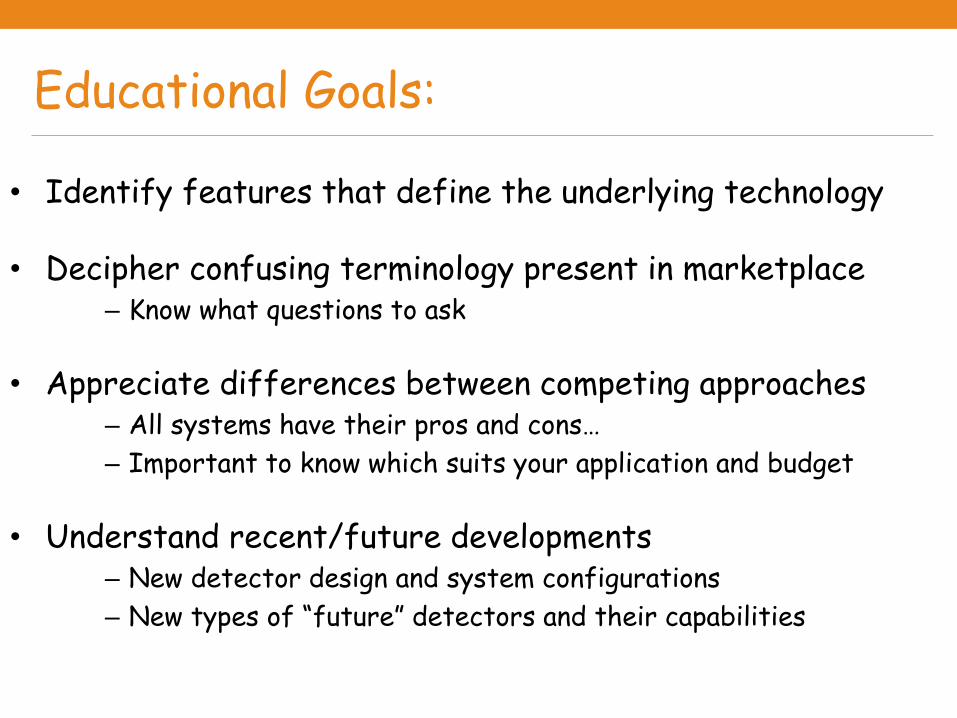
Educational Goals:
• Identify features that define the underlying technology
• Decipher confusing terminology present in marketplace – Know what questions to ask
• Appreciate differences between competing approaches – All systems have their pros and cons…
– Important to know which suits your application and budget
• Understand recent/future developments – New detector design and system configurations
– New types of “future” detectors and their capabilities
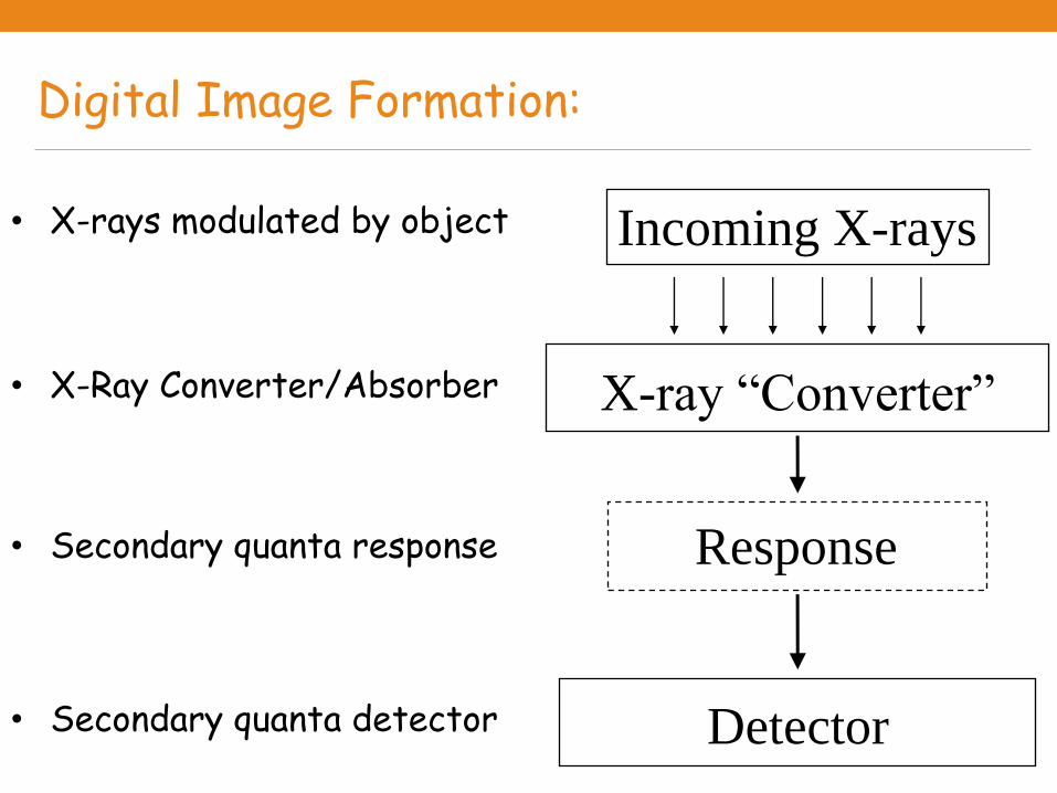
Digital Image Formation:
Detector
• X-Ray Converter/Absorber
• Secondary quanta detector
Response
Incoming X-rays
X-ray “Converter”
• X-rays modulated by object
• Secondary quanta response

Outline:
• Discuss x-ray absorption material selection
• Review secondary quantum detection options
• Review current status of projection x-ray technology – Highlight new developments in designs and their rationale
• Review future detector developments – New configurations (e.g. flexible substrates, “smart pixels”)
– New capabilities (e.g. photon counting and energy resolution)
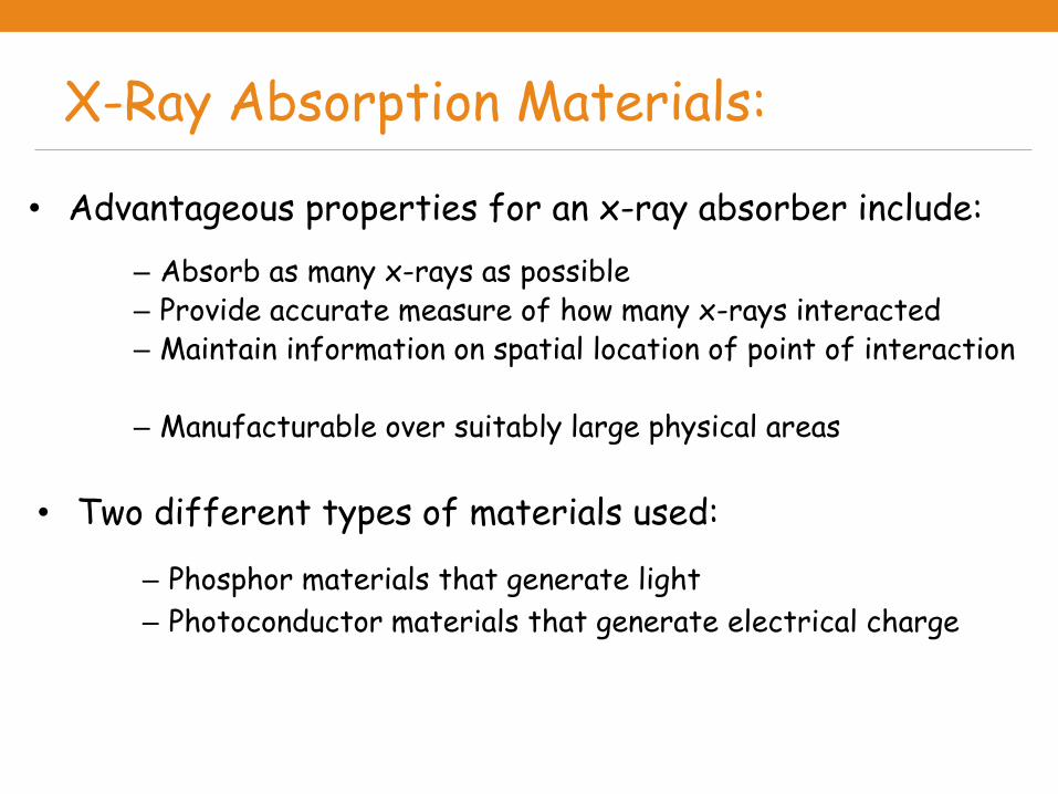
X-Ray Absorption Materials:
• Advantageous properties for an x-ray absorber include:
– Absorb as many x-rays as possible – Provide accurate measure of how many x-rays interacted – Maintain information on spatial location of point of interaction
– Manufacturable over suitably large physical areas
• Two different types of materials used:
– Phosphor materials that generate light
– Photoconductor materials that generate electrical charge
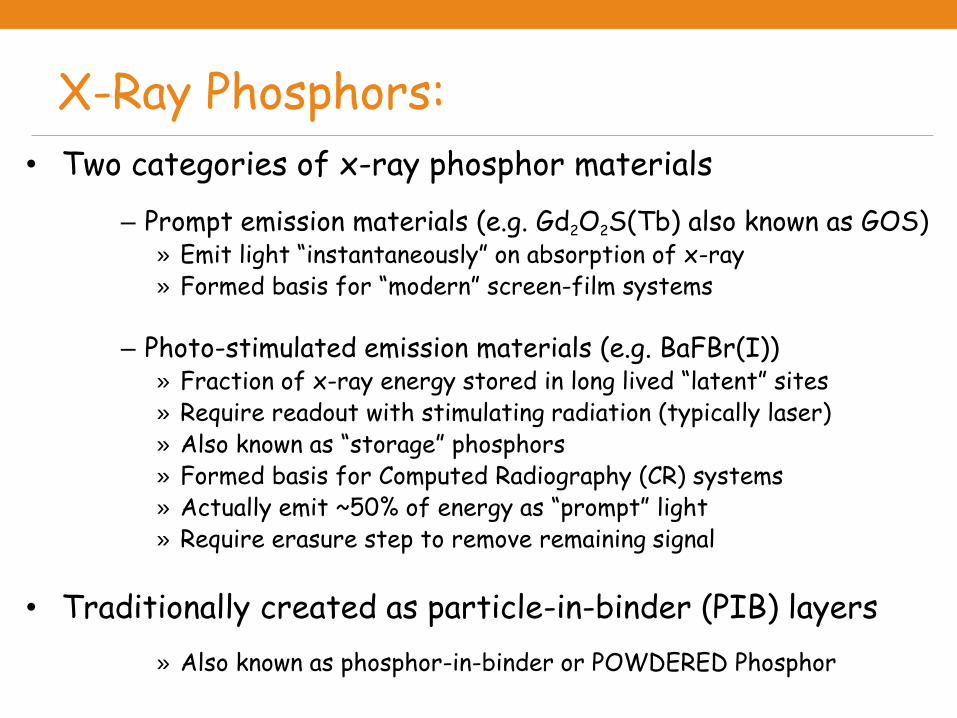
X-Ray Phosphors:
• Two categories of x-ray phosphor materials
– Prompt emission materials (e.g. Gd2O2S(Tb) also known as GOS) » Emit light “instantaneously” on absorption of x-ray » Formed basis for “modern” screen-film systems
– Photo-stimulated emission materials (e.g. BaFBr(I)) » Fraction of x-ray energy stored in long lived “latent” sites » Require readout with stimulating radiation (typically laser) » Also known as “storage” phosphors » Formed basis for Computed Radiography (CR) systems » Actually emit ~50% of energy as “prompt” light » Require erasure step to remove remaining signal
• Traditionally created as particle-in-binder (PIB) layers
» Also known as phosphor-in-binder or POWDERED Phosphor

X-Ray Phosphors:
~100-150 mm
binder
phosphor
Air gaps
• PIB configured from small phosphor grains in plastic – Relatively “easy” to manufacture (after decades of development) – Very physically robust
• Issue with creating thick layers to increase absorption – Light scatters within material – As thickness increases so does light spreading
» Reduces resolution and increases noise (Lubberts effect) – Escape efficiency of light from screen varies through screen depth
» Also results in increased noise (Swank noise)

X-Ray Phosphors: • More recently “structured” phosphors have been used
– Prompt emission type: CsI(Tl) – Stimulated emission type: CsBr(Eu) – Reduces effect of thickness on spatial resolution: allows thicker layers – Improves light escape efficiency so reduces Swank noise – Allows higher “packing fraction” than PIB so higher effective absorption
4 mm
~200 mm Mammo.
~500-600 mm Gen. Rad.

X-Ray Photoconductors:
• Somewhat different issues than phosphors:
– Require applied voltage to “energize” layer and allow charge collection
– Internal field constrains lateral drift of released charges
– Near perfect spatial resolution almost independent of thickness
– High collection efficiency so low Swank noise
– Most mature material is amorphous selenium (Z=34)
» Low Z value limits x-ray absorption at diagnostic energies (>60kVp)
» Difficult to manufacture thick layers (~1000mm) over large area
» More suited to mammographic applications (<30kVp)
– Other materials include c-Si, CdTe, CdZnTe, HgI, PbI, PbO, Xenon.
E H.V. ~10V/mm
~200 mm Mammo.
~500-1000 mm Gen.Rad.
1.E-01
1.E+00
1.E+01
1.E+02
1.E+03
1.E+04
0 20 40 60 80 100 120 140
Photon Energy (keV)
Att
enua
tion C
oeff
icient
(mu)
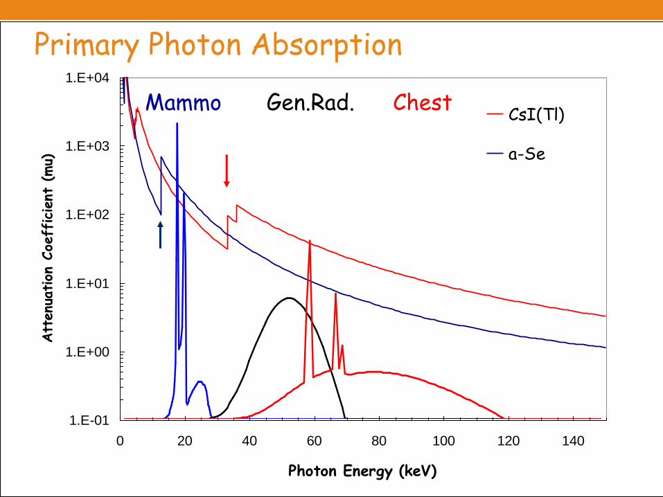
CsI(Tl)
a-Se
Primary Photon Absorption
Mammo Gen.Rad. Chest
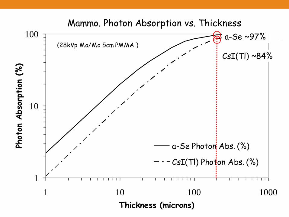
Mammo. Photon Absorption vs. Thickness
1
10
100
1 10 100 1000
Thickness (microns)
Phot
on A
bso
rption
(%)
a-Se Photon Abs. (%)
CsI(Tl) Photon Abs. (%)
(28kVp Mo/Mo 5cm PMMA )a-Se ~97%
CsI(Tl) ~84%

RQA-9 Photon Absorption vs. Thickness
1
10
100
10 100 1000
Thickness (microns)
Phot
on A
bso
rpti
on (
%)
CsI(Tl) Photon Abs. (%)
a-Se Photon Abs. (%)
a-Se ~27%
CsI(Tl) ~56%

500mm CsI(Tl) 500mm a-Se
Clinical Image Comparisons: Lateral Chest (120kVp)

X-Ray Absorption Materials Summary:
• Can be divided into 3 main types:
– Prompt emitting phospors (Gd2O2S(Tb), CsI(Tl)) – Stimulated emission phosphors (BaFBr(I), CsBr(Eu)) – Photoconductors (a-Se)
• Phosphors can be sub-divided into:
– Powdered or Particle-in-binder layers – Structured/Needle/Focused Phosphors
• All have sufficiently good properties to be “useful”
• Which is “best” depends on specifics of application
Secondary Quanta Detection:
• Issues are similar for phosphors and photoconductors
– Need accurate measure of generated signal over large areas
– Maintain image “quality” produced by x-ray absorption layer
• Possible approaches include
– Point by point scanning
– Line scanning
– Full area readout

Point by Point Scanning:
• Storage Phosphors/CR lend themselves to this approach
– Image information “stored” in phosphor till scanned
– Allow time to scan whole area with small laser spot
– Spot ~100mm in size, 10mW power,
– Dwell time ~few msecs/pixel
– ~30 or so seconds for full readout
v
Laser Spot
Point by Point Scanning:
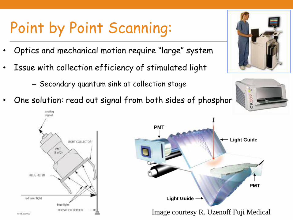
• Optics and mechanical motion require “large” system
• Issue with collection efficiency of stimulated light
– Secondary quantum sink at collection stage
• One solution: read out signal from both sides of phosphor
PMT
Light Guide
Light Guide
PMT
Image courtesy R. Uzenoff Fuji Medical

Point by Point Scanning:
• NovaRay’s ScanCathTM
inverse geometry system (SBDX)
• Uses large area source and small area detector
– Pixellated CdZnTe photon counting detector
– Transmission anode target with collimator
– Excellent scatter rejection
– Targetted to cardiac imaging at 30 fps.
– Automatically collects tomosynthesis data

Line/Slot Scanning: • To improve scan speed read out a line at a time.
• With storage phosphor can readout lines after area exposure
– Incorporate line laser and solid state collector in compact single unit
– Significantly reduces space requirements for beam path optics
– Still requires mechanical motion
– Also possible with photoconductor ( e.g Thoravision)
Laser Source + Intensity Control
Beam Shaping Photodetector
Optical Filter
Light Collection Optics
Image Plate
Philips Thoravision a-Se Chest System (Agfa)

Line/Slot Scanning:
• With prompt emitting phosphors need to collimate x-rays
• Numerous versions of line/slot scanned systems
• Most use some form of linear CCD as detector
– c-Si photon counting mammo system recently approved by FDA
– Gas wire chamber based systems have also been reported
• Good coupling between phosphor and CCD, good DQE
• Excellent scatter rejection
• Still require mechanical motion and collimation alignment
• Scan times of multiple seconds
• Commercial examples that used CsI(Tl) coupled & linear CCD’s include:
– Thorascan (Oldelft) chest system – Senoscan (Fischer) mammo system

Line/Slot Scanning:
•Lodox Statscan •Full body scan 13 secs •Linear CCD with CsI(Tl)
Line/Slot Scanning:
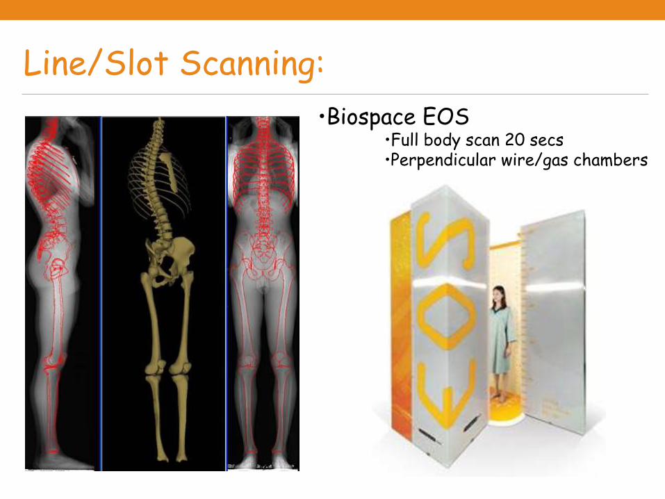
•Biospace EOS •Full body scan 20 secs •Perpendicular wire/gas chambers
Philips MicroDose
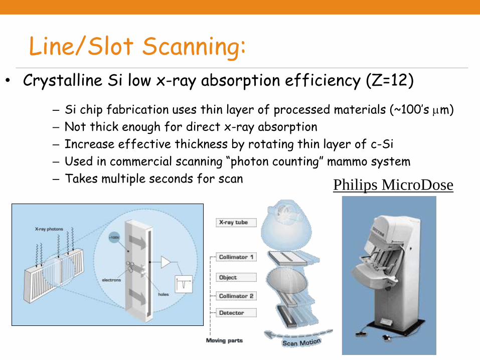
Line/Slot Scanning: • Crystalline Si low x-ray absorption efficiency (Z=12)
– Si chip fabrication uses thin layer of processed materials (~100’s mm)
– Not thick enough for direct x-ray absorption
– Increase effective thickness by rotating thin layer of c-Si
– Used in commercial scanning “photon counting” mammo system
– Takes multiple seconds for scan

Full Area “Electronic” Readout:
• Earliest approaches used CCD detectors
3-4cm
43cm
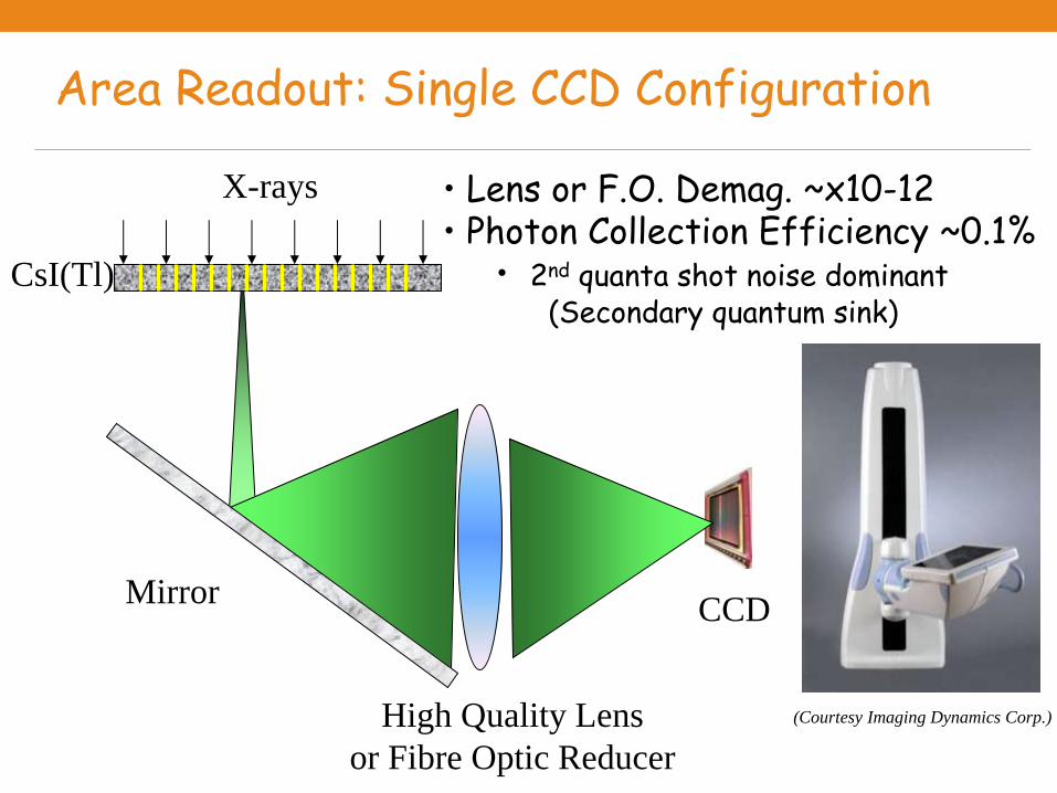
Area Readout: Single CCD Configuration
CsI(Tl)
Mirror CCD
X-rays • Lens or F.O. Demag. ~x10-12 • Photon Collection Efficiency ~0.1%
• 2nd quanta shot noise dominant (Secondary quantum sink)
High Quality Lens
or Fibre Optic Reducer
(Courtesy Imaging Dynamics Corp.)

Area Readout: Multiple CCD Configuration
• SwissRay and Apelem
• reduces de-mag.
(Source: SwissRay Corp.)
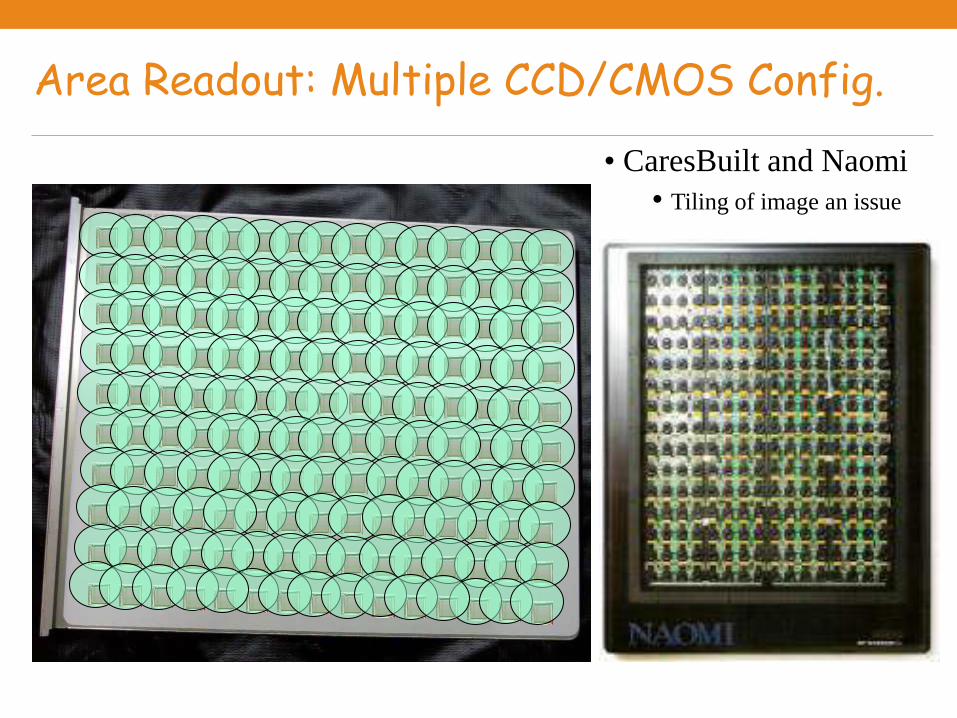
Area Readout: Multiple CCD/CMOS Config.
• CaresBuilt and Naomi
• Tiling of image an issue

Area Readout: a-Si:H Flat Panel Readout
• Fabricated using large area a-Si:H deposition facilities • 14x17” or larger readily available with pixels down to <100mm
• Can use prompt emitting phosphor or photoconductor
• Directly coupled to x-ray absorption layer (high transfer effic.)
• “Electronic” readout can operated in static or fluoroscopic modes
Sharp Gen. 10 Glass Substrate 9x10’

(Image courtesy Dr. B. Polischuk)
Area Readout: a-Si:H Flat Panel Readout
43x43cm
Pixel Area
Switching
Element
Sensing/Storage
Element

Area Readout: a-Si:H Flat Panel Readout
• Advantages of a-Si:H readout arrays – Large area fabrication (>40cm dimensions) allowing non-tiled detector – “Mature” fabrication infrastructure (based on display industry)
– Many peripheral components now available “off-the-shelf” – Excellent image quality due to high 2nd quanta collection efficiency – True “electronic” readout (no mechanical moving parts) – Advanced application capable (i.e. supports “real-time” readout speeds) – Very tolerant of radiation damage (due to amorphous structure)
• Challenges for a-Si:H readout arrays – Relatively high “additive” electroinc noise
– Compromises low exposure perfomance – Fabricated on “fragile” glass substrates (0.5mm thick or less) – Inherent materials properties affect “image quality”
– Low carrier mobility limits “smart” pixel capabilities – Large feature sizes may limit “fill factor” of small pixels

Recent Developments: a-Si:H Portable Systems
•Recently, portable 14x17” & 17x17” detectors introduced • Initially rather heavy/bulky/thick with tether
• More recently wireless, battery powered with cassette form factor
• Smaller sized detectors (10x12”) now being introduced

• Synchronization between detector & x-ray delivery essential • Unlike screen/film and CR which are always “active”
• Traditional flat panel detectors integrated with generator
• New approaches have no hardwired “electrical” interface • Makes retrofitting of older systems easier
Recent Developments: Beam Triggered Readout
Konica Aero Sync TM

• Concept previously used in film/screen mammography
• Most advantageous when: • Energy deposition weighted towards entry side of screen (e.g. mammo)
• Have low x-ray absorption substrate
• Can reduce Swank noise and Lubberts Effect hence improving IQ
Recent Developments: Back Screen Config.
Substrate
Phosphor
Pixels
Front Screen Config.
Signal Spread
Incident X-Rays Incident X-Rays
Back Screen Config.

From: Ito et.al. SPIE Phys. Med. Imaging 8668 (2013) 866807-1
• Numerous research groups reported on pixel level circuitry • Main goal to amplify signal level to reduce effect of addt. noise
• Issue with size of a-Si:H TFT’s which can reduce fill factor
• First large area demonstration of multiple TFT a-Si:H pixels • 17x17” CsI detector, 150um pixels
• 1x1 or 2x2 binning at pixel level
• Improves noise performance • Adds signals before digitization
Recent Developments: Smart Pixels

• New substrate materials • Flexible substrates e.g. plastic, metal & glass (~0.1mm thick !)
• These would allow conformable, large area, very robust detectors
•Available 30cmx300m for roll-to-roll proc.
• New fabrication materials • Low temperature poly-Si
• Has improved carrier mobilities
• IGZO • Compatible with large area deposition
• Has better carrier mobility hence smaller feature sizes
• Allows more complex circuitry at pixel level
• New X-ray converters for lower dose applications • Mostly photoconductors that generate more signal per x-ray
(e.g. PbI, HgI, CdTe, CdZTe, PbO)
• Still mainly academic and commercial research activities
Corning Willow GlassTM
Recent Developments: New Materials
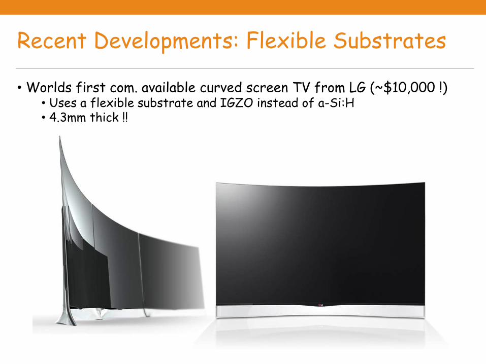
Recent Developments: Flexible Substrates
• Worlds first com. available curved screen TV from LG (~$10,000 !) • Uses a flexible substrate and IGZO instead of a-Si:H • 4.3mm thick !!

Area Readout: CMOS Technology
• Fabricated with “standard” silicon IC chip technology
•Typically use standard 8” Si wafer fab. capability
• Limits physical dimensions of sensor
•Small feature size (<10nm) allows complex pixels
• e.g. Pixel level amplification, and dose sensing
• Larger sensor tiles can reduce yield and increase cost
8 inch 12 inch 18 inch (Intel)
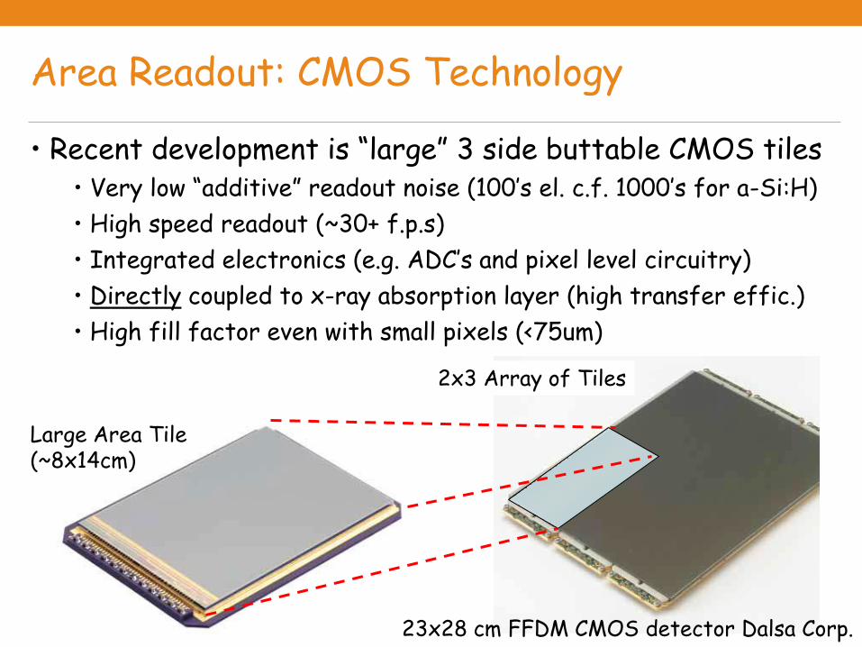
Large Area Tile (~8x14cm)
• Recent development is “large” 3 side buttable CMOS tiles • Very low “additive” readout noise (100’s el. c.f. 1000’s for a-Si:H)
• High speed readout (~30+ f.p.s)
• Integrated electronics (e.g. ADC’s and pixel level circuitry)
• Directly coupled to x-ray absorption layer (high transfer effic.)
• High fill factor even with small pixels (<75um)
23x28 cm FFDM CMOS detector Dalsa Corp.
2x3 Array of Tiles
Area Readout: CMOS Technology

• CMOS allows energy integrating or photon counting • Energy integrating typically utilizes CsI or GOS bonded to chip
• Photon counting typically uses photoconductor (CdTe or CdZnTe)
• Use of CdTe and CdZnTe currently limits size of sensor to < ~2-5 cm
• Energy selective imaging is possible
• Photons can be weighted according to image information “content”
Area Readout: CMOS Technology
•Energy resolved photon counting allows multi-spectral imaging

Summary:
• Knowing the basic components allows for informed choices.
• Storage phosphor systems: Faster, smaller and cheaper
• Slow readout speeds prevent “real time” use
• a-Si:H Flat Panels: Form factor and functionality (and price!)
• New materials continue to be investigated
• Watch for developments in display manufacturing (e.g use of IGZO)
• CMOS: Increasing commercial visibility and viability
• Confined to smaller area applications at present (tiled arrays)
• Dental intra-oral, mammography, small field fluoro, CBCT
• Excellent image quality and energy selective imaging capabilities


Performance Summary: Point/Line Scanning
Full Area Readout
Stimulated Emission Phosphor
Prompt Emission Phosphor Photoconductor
BaFBr(I) CsBr(Eu) a-Si:H +GOS
a-Si:H +CsI(Tl)
CCD/CMOS lens/fib.opt.
Tiled CMOS
200mm a-Se (mammo)
500mm a-Se (gen.rad.)
Speed of Readout
- - (+ if integ.)
- (+ if integ.)
+ + + + + + + + + + + + + +
Image Quality
+ + + + + + + + + + + + + + + + +
Robustness + ++ - + + + - + + + + + - - -
Size - - - + + - - + + +
Cost + + + + - - + + + - - -
Adv. Apps. (tomo& DE)
- - + + + + + + + + + +

![Neuroimag Clin N Am 16 (2006) 529–552 Opioid Imaging · tiple receptors [4]. In the early 1980s, there was ev-idence for the existence of at least three types of opiate receptors:](https://img.dokumen.tips/doc/110x75/5f63111ec9a74e2dd84c2697/neuroimag-clin-n-am-16-2006-529a552-opioid-imaging-tiple-receptors-4-in-the.jpg)