Embed Size (px)
Citation preview
International Research Journal of Engineering and Technology (IRJET) e-ISSN: 2395 -0056
Volume: 03 Issue: 04 | Apr-2016 www.irjet.net p-ISSN: 2395-0072
© 2016, IRJET | Impact Factor value: 4.45 | ISO 9001:2008 Certified Journal | Page 2463
Development of AlGaAs /GaAs/ AlGaAs Step Quantum well to produce Tunable
Photo Detector and Electro-Absorption Modulator for noise reduction
1Palasri Dhar,2Ananya Gangopadhyay
Gurunanak Institute of Engineering 157/F, Sodpur, Kolkata-700114
Email id: [email protected]
---------------------------------------------------------------------***---------------------------------------------------------------------Abstract: We design a Step Asymmetric Quantum well with AlGaAs /GaAs/ AlGaAs material. We derive the expression of absorption coefficient ,which is important in the development of Tunable Photo Detector and Electro-Absorption Modulator. The “staircase” potential method was used to present both the effects of external bias and the shift in the detection wavelength due to the various applied external electric fields across the asymmetric quantum well. The electro absorption optical modulator is an optical modulator that utilizes the electroabsorption effect that the optical Absorption Coefficient of a substance varies depending on the electric field applied to it.
1. Introduction:
Epitaxial crystal growth techniques such as Molecular beam
epitaxy or MOCVD allows to have monolayer upto 3 armstrong
control in the chemical composition of the crystal. Nearly every
semiconductor crystal such as GaAs, AlGaAs have been grown by
epitaxial growth. This allows the growth of Quantum well where
electronic properties can be altered. Quantum well systems are
used for high performance devices such as transistors, lasers,
modulators. Quantum wells offer a very useful approach to band
structure tailoring. In quantum wells electrons behave as if they
are in a 2-dimention space and acquire properties that are
specially useful for many optoelectronic application.
We are taking an AlGaAs-GaAs-AlGaAs material. Here a step
asymmetric quantum well is formed by sandwiching an
ultrathin film of AlGaN in between two GaNlayers.
Optoelectronic devices and systems use a variety of different
optical and electro optical effects. Quantum Heteostructures
provide a mean to enhance many of the effects known in bulk
like materials, such as exitonic effects and optical nonlinearities
near the fundamental edge of the optical absorption.
Heteostructure Quantum wells find wide applications in the
development of tunable infrared photo detector and
electroabsorption optical modulator. The electroabsorption
optical modulator is an optical modulator that utilizes the
electro absorption effect that the optical Absorption Coefficient
of substance varies depending on the electric field applied to it.
[6]
2.Step asymmetric quantum well:
Step quantum well can also be called a staircase structure .This
type of structure consists of a stack of quantum wells. When the
quantum well is adequately deep and narrow, its energy states
are quantized. The potential depth and width of the well can be
adjusted so that it has only two energy states: a ground state
near the well bottom and a first excited state near the well top. If
an external bias is applied in this type of quantum well, a
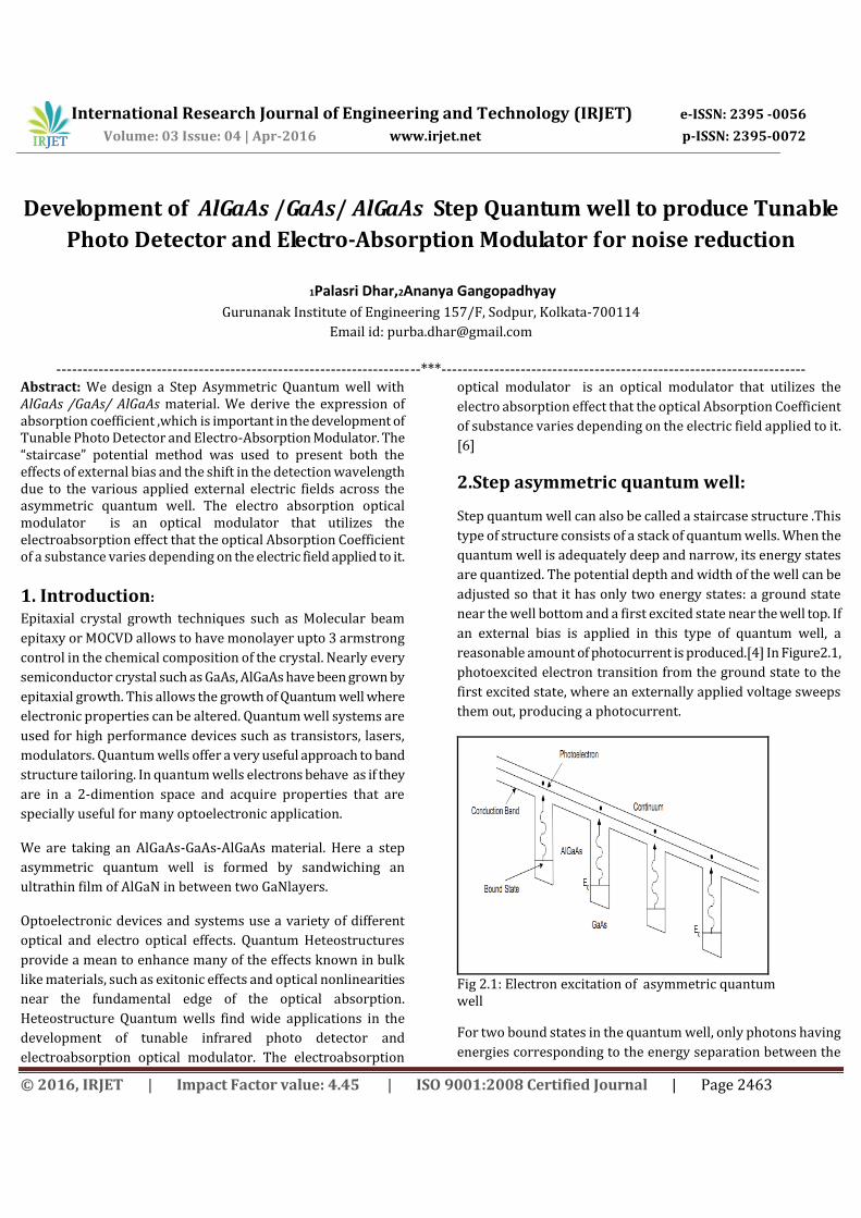
reasonable amount of photocurrent is produced.[4] In Figure2.1,
photoexcited electron transition from the ground state to the
first excited state, where an externally applied voltage sweeps
them out, producing a photocurrent.
Fig 2.1: Electron excitation of asymmetric quantum well
For two bound states in the quantum well, only photons having
energies corresponding to the energy separation between the
International Research Journal of Engineering and Technology (IRJET) e-ISSN: 2395 -0056
Volume: 03 Issue: 04 | Apr-2016 www.irjet.net p-ISSN: 2395-0072
© 2016, IRJET | Impact Factor value: 4.45 | ISO 9001:2008 Certified Journal | Page 2464
two states are absorbed, resulting in a photodetector with a
sharp absorption spectrum. If there is only one bound state in
the well, the transition occurs between the bound state and the
continuum, producing a broader peak.[5]
Now designing a quantum well to detect light of a particular
wavelength becomes a straightforward matter of adjusting the
potential depth and width of the well to produce two states,
separated by the desired photon energy.
The Schrödinger equation is solved numerically using the
transfer matrix approach. In this case the Figure 2.2 is taken into
account. The effect of the electric field on the energy levels will
be incorporated by the “staircase” approximation of the linear
potential
Fig 2.2: Arbitrary multi- layered potential well structure
2.1: Intersubband transition selection rules:
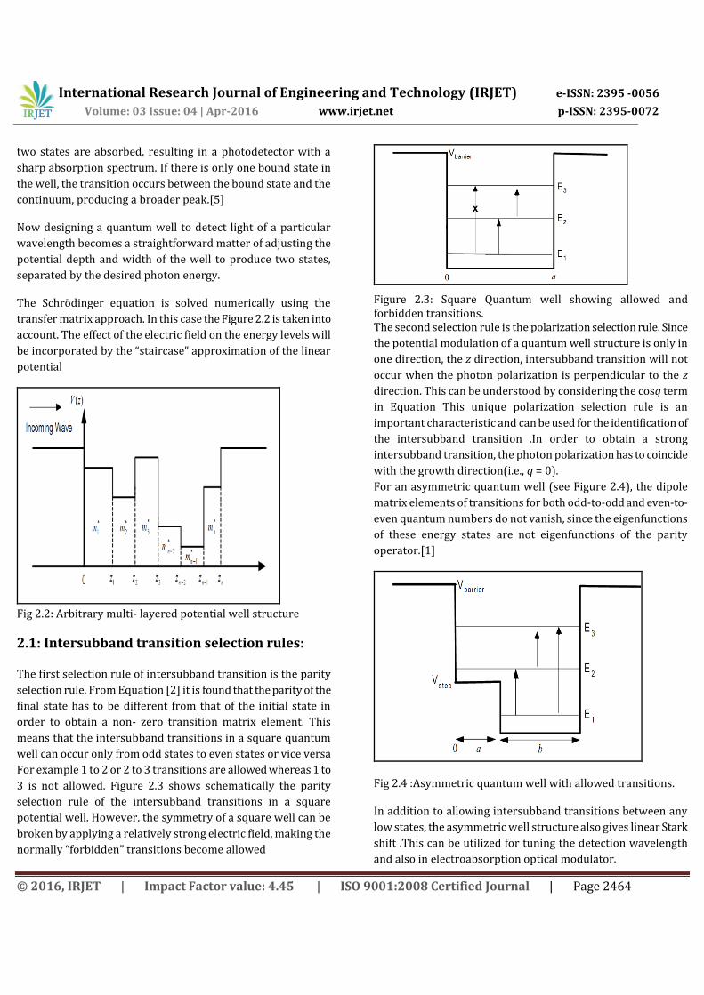
The first selection rule of intersubband transition is the parity
selection rule. From Equation [2] it is found that the parity of the
final state has to be different from that of the initial state in
order to obtain a non- zero transition matrix element. This
means that the intersubband transitions in a square quantum
well can occur only from odd states to even states or vice versa
For example 1 to 2 or 2 to 3 transitions are allowed whereas 1 to
3 is not allowed. Figure 2.3 shows schematically the parity
selection rule of the intersubband transitions in a square
potential well. However, the symmetry of a square well can be
broken by applying a relatively strong electric field, making the
normally “forbidden” transitions become allowed
Figure 2.3: Square Quantum well showing allowed and forbidden transitions. The second selection rule is the polarization selection rule. Since
the potential modulation of a quantum well structure is only in
one direction, the z direction, intersubband transition will not
occur when the photon polarization is perpendicular to the z
direction. This can be understood by considering the cosq term
in Equation This unique polarization selection rule is an
important characteristic and can be used for the identification of
the intersubband transition .In order to obtain a strong
intersubband transition, the photon polarization has to coincide
with the growth direction(i.e., q = 0).
For an asymmetric quantum well (see Figure 2.4), the dipole
matrix elements of transitions for both odd-to-odd and even-to-
even quantum numbers do not vanish, since the eigenfunctions
of these energy states are not eigenfunctions of the parity
operator.[1]
Fig 2.4 :Asymmetric quantum well with allowed transitions.
In addition to allowing intersubband transitions between any
low states, the asymmetric well structure also gives linear Stark
shift .This can be utilized for tuning the detection wavelength
and also in electroabsorption optical modulator.
International Research Journal of Engineering and Technology (IRJET) e-ISSN: 2395 -0056
Volume: 03 Issue: 04 | Apr-2016 www.irjet.net p-ISSN: 2395-0072
© 2016, IRJET | Impact Factor value: 4.45 | ISO 9001:2008 Certified Journal | Page 2465
2.3.Intersubband absorption coefficient:
The absorption coefficient in quantum well devices is one of the
most important factor in the design of the quantum structures
and is proportional to the amount of incident light that is
absorbed in the structure. The absorption coefficient depends
upon the material characteristics of the respective
semiconductor. For example, the high refractive index of a
semiconductor such as GaAs,(n = 3.3), causes that light incident
on the surface of an epitaxial layer structure is refracted
towards the normal (n = 3.3), causes that light incident on the
surface of an epitaxial layer structure is refracted towards the
normal for example, and away from the required orientation.
Efficient coupling of the intersubband transition can be achieved
by a number of optical techniques, including the use of a beveled
edged device, diffraction gratings, and combined diffraction
gratings and waveguides.[3]
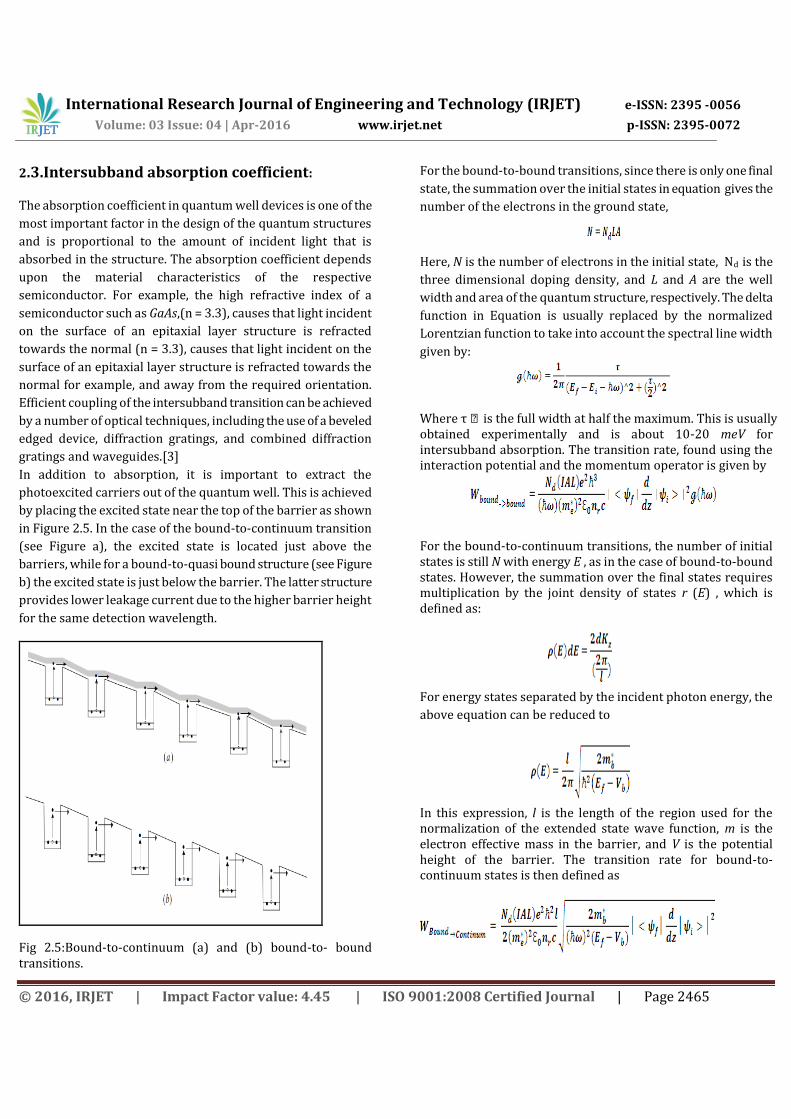
In addition to absorption, it is important to extract the
photoexcited carriers out of the quantum well. This is achieved
by placing the excited state near the top of the barrier as shown
in Figure 2.5. In the case of the bound-to-continuum transition
(see Figure a), the excited state is located just above the
barriers, while for a bound-to-quasi bound structure (see Figure
b) the excited state is just below the barrier. The latter structure
provides lower leakage current due to the higher barrier height
for the same detection wavelength.
Fig 2.5:Bound-to-continuum (a) and (b) bound-to- bound transitions.
For the bound-to-bound transitions, since there is only one final
state, the summation over the initial states in equation gives the
number of the electrons in the ground state,
Here, N is the number of electrons in the initial state, Nd is the
three dimensional doping density, and L and A are the well
width and area of the quantum structure, respectively. The delta
function in Equation is usually replaced by the normalized
Lorentzian function to take into account the spectral line width
given by:
Where τ is the full width at half the maximum. This is usually obtained experimentally and is about 10-20 meV for intersubband absorption. The transition rate, found using the interaction potential and the momentum operator is given by
For the bound-to-continuum transitions, the number of initial states is still N with energy E , as in the case of bound-to-bound states. However, the summation over the final states requires multiplication by the joint density of states r (E) , which is defined as:
For energy states separated by the incident photon energy, the
above equation can be reduced to
In this expression, l is the length of the region used for the normalization of the extended state wave function, m is the electron effective mass in the barrier, and V is the potential height of the barrier. The transition rate for bound-to-continuum states is then defined as
International Research Journal of Engineering and Technology (IRJET) e-ISSN: 2395 -0056
Volume: 03 Issue: 04 | Apr-2016 www.irjet.net p-ISSN: 2395-0072
© 2016, IRJET | Impact Factor value: 4.45 | ISO 9001:2008 Certified Journal | Page 2466
This model of the bound to free intersubband absorption is one where the line width is due only to the variation of the joint density of states.[5] The absorption coefficient can be obtained by using both the transition of the matrix element and the transition rate as follows:
Thus, the absorption coefficients for the bound-to-bound and
bound-to-continuumtransitions are given by
The length term, l , which appears in the bound-to-continuum transition, is eliminated in the normalized final state wave function (assuming it is confined to a length,l).
2.4 Result Analysis:
-6 -4 -2 0 2 4 6 8
x 10-9
0
0.05
0.1
0.15
0.2
0.25
0.3
0.35
a = 1 nm , b = 0.9 nm
Energ
y (
eV
)
0.4 / 0.2 / 0.4
E1=0.236 ev
E2=0.2992 ev
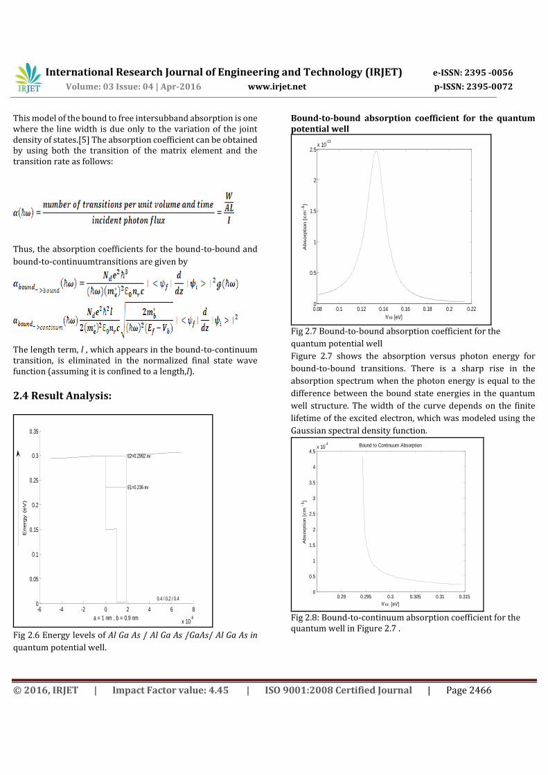
Fig 2.6 Energy levels of Al Ga As / Al Ga As /GaAs/ Al Ga As in
quantum potential well.
Bound-to-bound absorption coefficient for the quantum potential well
0.08 0.1 0.12 0.14 0.16 0.18 0.2 0.220
0.5
1
1.5
2
2.5x 10
-13
h [eV]
Absorp
tion [
cm
-1]
Fig 2.7 Bound-to-bound absorption coefficient for the
quantum potential well
Figure 2.7 shows the absorption versus photon energy for
bound-to-bound transitions. There is a sharp rise in the
absorption spectrum when the photon energy is equal to the
difference between the bound state energies in the quantum
well structure. The width of the curve depends on the finite
lifetime of the excited electron, which was modeled using the
Gaussian spectral density function.
0.29 0.295 0.3 0.305 0.31 0.3150
0.5
1
1.5
2
2.5
3
3.5
4
4.5x 10
-4
h [eV]
Absorp
tion [
cm
-1]
Bound to Continuum Absorption
Fig 2.8: Bound-to-continuum absorption coefficient for the quantum well in Figure 2.7 .
International Research Journal of Engineering and Technology (IRJET) e-ISSN: 2395 -0056
Volume: 03 Issue: 04 | Apr-2016 www.irjet.net p-ISSN: 2395-0072
© 2016, IRJET | Impact Factor value: 4.45 | ISO 9001:2008 Certified Journal | Page 2467
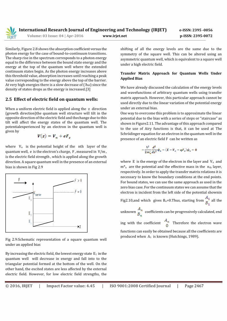
Similarly, Figure 2.8 shows the absorption coefficient versus the photon energy for the case of bound-to-continuum transitions. The sharp rise in the spectrum corresponds to a photon energy equal to the difference between the bound state energy and the energy at the top of the quantum well where the extended continuum states begin. As the photon energy increases above this threshold value, absorption increases until reaching a peak value corresponding to the energy above the top of the barrier. At very high energies there is a slow decrease of (’ћω) since the density of states drops as the energy is increased.[3]
2.5 Effect of electric field on quantum wells:
When a uniform electric field is applied along the z direction (growth direction)the quantum well structure will tilt in the opposite direction of the electric field and thechange due to this tilt will affect the energy states of the quantum well. The potentialexperienced by an electron in the quantum well is given by
where Vn is the potential height of the nth layer of the
quantum well, e is the electron’s charge, F , measured in V/m ,
is the electric field strength , which is applied along the growth
direction. A square quantum well in the presence of an external
bias is shown in Fig 2.9
Fig 2.9:Schematic representation of a square quantum well
under an applied bias
By increasing the electric field, the lowest energy state E1 in the
quantum well will decrease in energy and fall into to the
triangular potential formed at the bottom of the well. On the
other hand, the excited states are less affected by the external
electric field. However, for low electric field strengths, the
shifting of all the energy levels are the same due to the
symmetry of the square well. This can be altered using an
asymmetric quantum well, which is equivalent to a square well
under a high electric field.
Transfer Matrix Approach for Quantum Wells Under
Applied Bias
We have already discussed the calculation of the energy levels
and wavefunctions of arbitrary quantum wells using transfer
matrix approach. However, this particular approach cannot be
used directly due to the linear variation of the potential energy
under an external bias.
One way to overcome this problem is to approximate the linear
potential due to the bias with a series of steps or “staircase” as
shown in Figure2.11. The advantage of this approach compared
to the use of Airy functions is that, it can be used at The
Schrödinger equation for an electron in the quantum well in the
presence of an electric field F can be written as
where E is the energy of the electron in the layer and Vn and
m*n are the potential and the effective mass in the nth layer,
respectively. In order to apply the transfer matrix relations it is
necessary to know the boundary conditions at the end points.
For bound states, we can use the same approach as used in the
zero bias case. For the continuum states we can assume that the
electron is incident from the left side of the potential shownin
Fig2.10,and which gives Bn=0.Thus, starting from all the
unknown coefficients can be progressively calculated, end
ing with the coefficient Therefore the electron wave
functions can easily be obtained because all the coefficients are
produced when A1 is known (Hutchings, 1989).
International Research Journal of Engineering and Technology (IRJET) e-ISSN: 2395 -0056
Volume: 03 Issue: 04 | Apr-2016 www.irjet.net p-ISSN: 2395-0072
© 2016, IRJET | Impact Factor value: 4.45 | ISO 9001:2008 Certified Journal | Page 2468
Fig 2.10:The stair case approximation of the potential
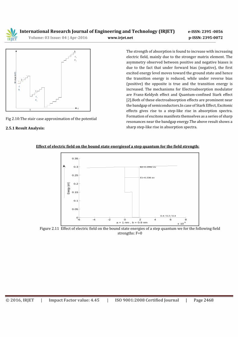
2.5.1 Result Analysis:
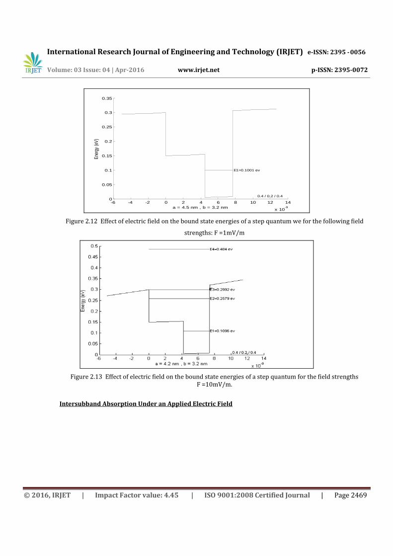
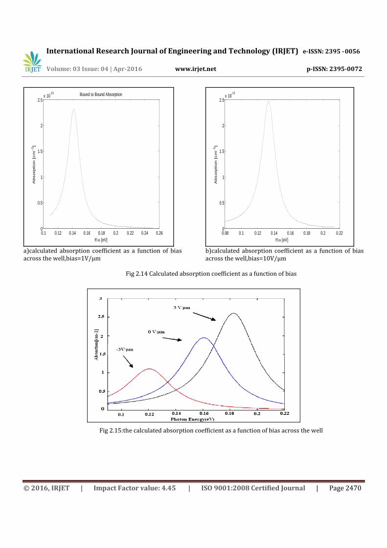
The strength of absorption is found to increase with increasing
electric field, mainly due to the stronger matrix element. The
asymmetry observed between positive and negative biases is
due to the fact that under forward bias (negative), the first
excited energy level moves toward the ground state and hence
the transition energy is reduced, while under reverse bias
(positive) the opposite is true and the transition energy is
increased. The mechanisms for Electroabsorption modulator
are Franz-Keldysh effect and Quantum-confined Stark effect
[2].Both of these electroabsorption effects are prominent near
the bandgap of semiconductors.In case of Stark Effect, Excitonic
effects gives rise to a step-like rise in absorption spectra.
Formation of excitons manifests themselves as a series of sharp
resonances near the bandgap energy.The above result shows a
sharp step-like rise in absorption spectra.
Effect of electric field on the bound state energiesof a step quantum for the field strength:
-6 -4 -2 0 2 4 6 8
x 10-9
0
0.05
0.1
0.15
0.2
0.25
0.3
0.35
a = 1 nm , b = 0.9 nm
Ene
rgy
(eV
)
0.4 / 0.2 / 0.4
E1=0.236 ev
E2=0.2992 ev
Figure 2.11 Effect of electric field on the bound state energies of a step quantum we for the following field strengths: F=0
Volume: 03 Issue: 04 | Apr-2016 www.irjet.net p-ISSN: 2395-0072
© 2016, IRJET | Impact Factor value: 4.45 | ISO 9001:2008 Certified Journal | Page 2469
-6 -4 -2 0 2 4 6 8 10 12 14
x 10-9
0
0.05
0.1
0.15
0.2
0.25
0.3
0.35
a = 4.5 nm , b = 3.2 nm
Ene
rgy
(eV
)
0.4 / 0.2 / 0.4
E1=0.1001 ev
Figure 2.12 Effect of electric field on the bound state energies of a step quantum we for the following field
strengths: F =1mV/m
Figure 2.13 Effect of electric field on the bound state energies of a step quantum for the field strengths F =10mV/m.
Intersubband Absorption Under an Applied Electric Field
International Research Journal of Engineering and Technology (IRJET) e-ISSN: 2395 -0056
Volume: 03 Issue: 04 | Apr-2016 www.irjet.net p-ISSN: 2395-0072
© 2016, IRJET | Impact Factor value: 4.45 | ISO 9001:2008 Certified Journal | Page 2470
0.1 0.12 0.14 0.16 0.18 0.2 0.22 0.24 0.260
0.5
1
1.5
2
2.5x 10
-13
h [eV]
Absorp
tion [
cm
-1]
Bound to Bound Absorption
a)calculated absorption coefficient as a function of bias across the well,bias=1V/μm
0.08 0.1 0.12 0.14 0.16 0.18 0.2 0.220
0.5
1
1.5
2
2.5x 10
-13
h [eV]
Absorp
tion [
cm
-1]
b)calculated absorption coefficient as a function of bias across the well,bias=10V/μm
Fig 2.14 Calculated absorption coefficient as a function of bias
Fig 2.15:the calculated absorption coefficient as a function of bias across the well
International Research Journal of Engineering and Technology (IRJET) e-ISSN: 2395 -0056
Volume: 03 Issue: 04 | Apr-2016 www.irjet.net p-ISSN: 2395-0072
© 2016, IRJET | Impact Factor value: 4.45 | ISO 9001:2008 Certified Journal | Page 2471
Conclusion: An attempt has been made design a Step Asymmetric Quantum well with AlGaAs /GaAs/ AlGaAs material. We derive the
exression of absorption coefficient which is important in the development of Tunable Photo Detector and Electro-Absorption
Modulator. Thereby, graphs are plotted with absorption co-efficient as a function of external bias across the well.So,this is
similar to the mechanisms of Photo Detector and Electro-Absorption Modulator . The mechanisms for Electroabsorption
modulator are Franz-Keldysh effect and Quantum-confined Stark effect .Both of these electro absorption effects are prominent
near the bandgap of semiconductors. In case of Stark Effect,Excitonic effects gives rise to a step-like rise in absorption
spectra.Formation of excitons manifests themselves as a series of sharp resonances near the bandgap energy. The above result
shows a sharp step-like rise in absorption spectra .The electro absorption optical modulator (EA modulator) is an optical
modulator that utilizes the electroabsorption effect that the optical Absorption Coefficient of a substance varies depending on
the electric field applied to it. The EA modulator is generally classified into a type using absorption Waveguide Layer having a
quantum well structure and a type using a bulk Semiconductor layer rather than a waveguide layer. Variable optical
attenuators (VOA) are used to permit dynamic control of Optical Power levels throughout a communications,
telecommunications or other transmission network. As traffic in networks increase. VOAs may be used to dynamically lower
the optical power levels depending on the length of the Network route so that appropriate power levels are received at the end
receivers. The performance of optical modulators may be affected by numerous factors, such as a change in the environmental
temperature.
For modulators in telecommunications small size and modulation voltages are desired. The EAM is candidate for use in external
modulation links in telecommunications. These modulators can be realized using either bulk semiconductor materials or
materials with multiple quantum dots or wells.
Semiconductor quantum well EAM is widely used to modulate near-infrared (NIR) radiation at frequencies below
0.1THz.Allows a single optical power source to be used for large number of information carrying beams.
References:
[1] Quantum Wells, Wires and Dots-Harrison P (Chichester: Wiley), 2000.
[2] Quantum heterostructure-Microelectronics and Optoelectronics –Vladimir Mittin, Viatcheslav A. Kochelap and Michael
A.Stroscio; Cambridge University Press.1999.
[3] Physics of Quantum Well Devices-B.R. Nag .
[4]AlGaN-based Ultraviolet Lasers - Applications and Materials Challenges Michael Kneissl, Tim Kolbe, Jessica Schlegel, Joachim
Stellmach, Chris Chua, Zhihong Yang, Arne Knauer, V. Küller, Markus Weyers, Noble M. Johnson.
[5] Ching-Fuh Lin, Member, ZEEE, Bor-Lin Lee, and Po-Chien Lin “Broad-Band Superluminescent Diodes Fabricated on a
substrate with asymmetric dual quantum well” in IEEE Photonics Technology Letters, Vol. 8, No. 11, November 1996.
International Research Journal of Engineering and Technology (IRJET) e-ISSN: 2395 -0056


![Optical characterization of type-I to type-II band alignment … · 2017-11-09 · GaAs/AlGaAs material system [2]. To date, many GaAs/ AlGaAs nanostructures, in particular QDs and](https://img.dokumen.tips/doc/110x75/5e99ea94c8c26a550d1cbb00/optical-characterization-of-type-i-to-type-ii-band-alignment-2017-11-09-gaasalgaas.jpg)