Embed Size (px)
Citation preview

http://www.cl.cam.ac.uk/~mgk25/sc99-tamper[-slides].pdf
Oliver Kömmerling
ADSR
Markus G. Kuhn
Computer Laboratory
Design Principles for Tamper-ResistantSmartcard Processors
λ
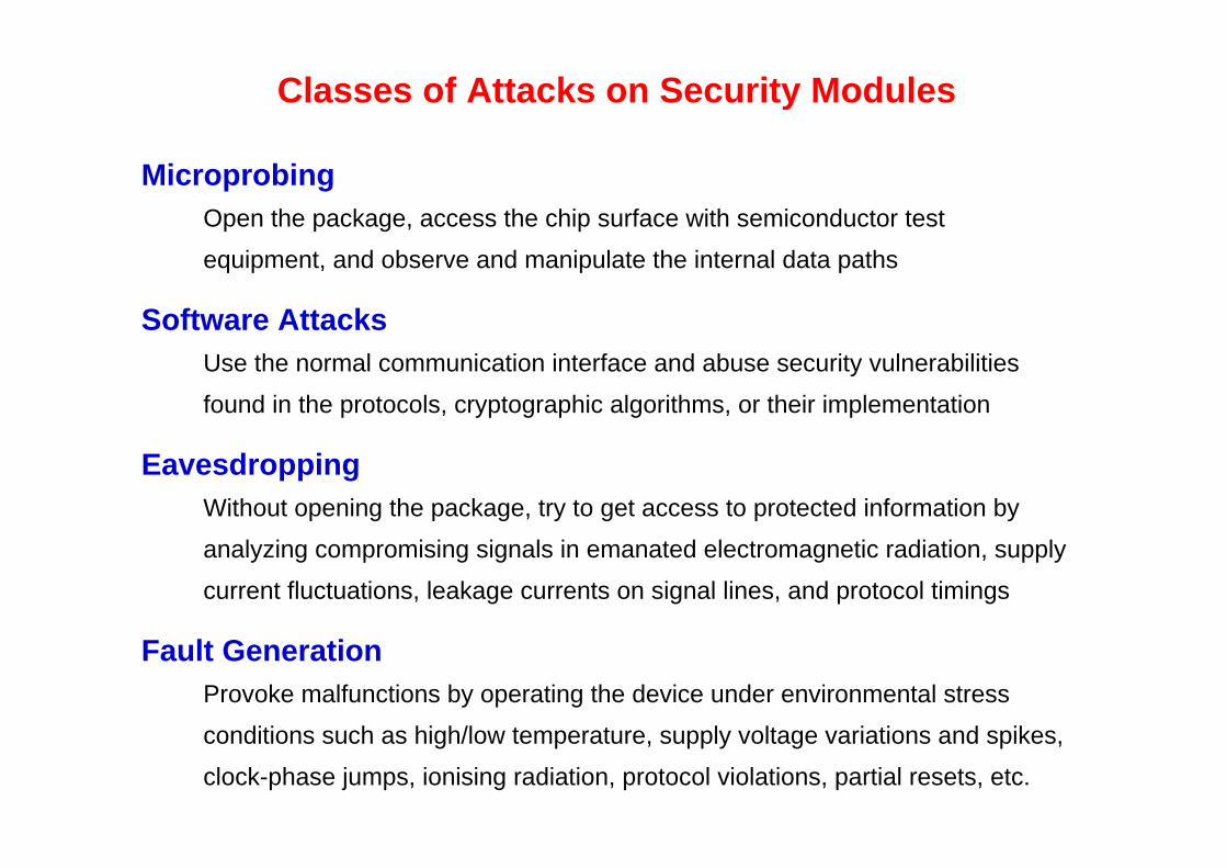
Classes of Attacks on Security Modules
Microprobing
Use the normal communication interface and abuse security vulnerabilities
Open the package, access the chip surface with semiconductor test
equipment, and observe and manipulate the internal data paths
EavesdroppingWithout opening the package, try to get access to protected information by
analyzing compromising signals in emanated electromagnetic radiation, supply
Fault GenerationProvoke malfunctions by operating the device under environmental stress
conditions such as high/low temperature, supply voltage variations and spikes,
found in the protocols, cryptographic algorithms, or their implementation
current fluctuations, leakage currents on signal lines, and protocol timings
Software Attacks
clock-phase jumps, ionising radiation, protocol violations, partial resets, etc.
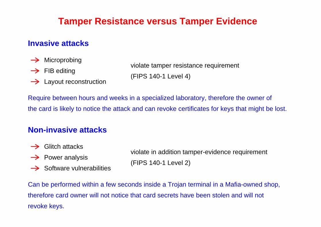
Microprobing
FIB editing
Layout reconstruction
Require between hours and weeks in a specialized laboratory, therefore the owner of
Glitch attacks
Power analysis
violate tamper resistance requirement
Invasive attacks
Non-invasive attacks
the card is likely to notice the attack and can revoke certificates for keys that might be lost.
revoke keys.
Tamper Resistance versus Tamper Evidence
(FIPS 140-1 Level 4)
(FIPS 140-1 Level 2)Software vulnerabilities
violate in addition tamper-evidence requirement
Can be performed within a few seconds inside a Trojan terminal in a Mafia-owned shop,
therefore card owner will not notice that card secrets have been stolen and will not
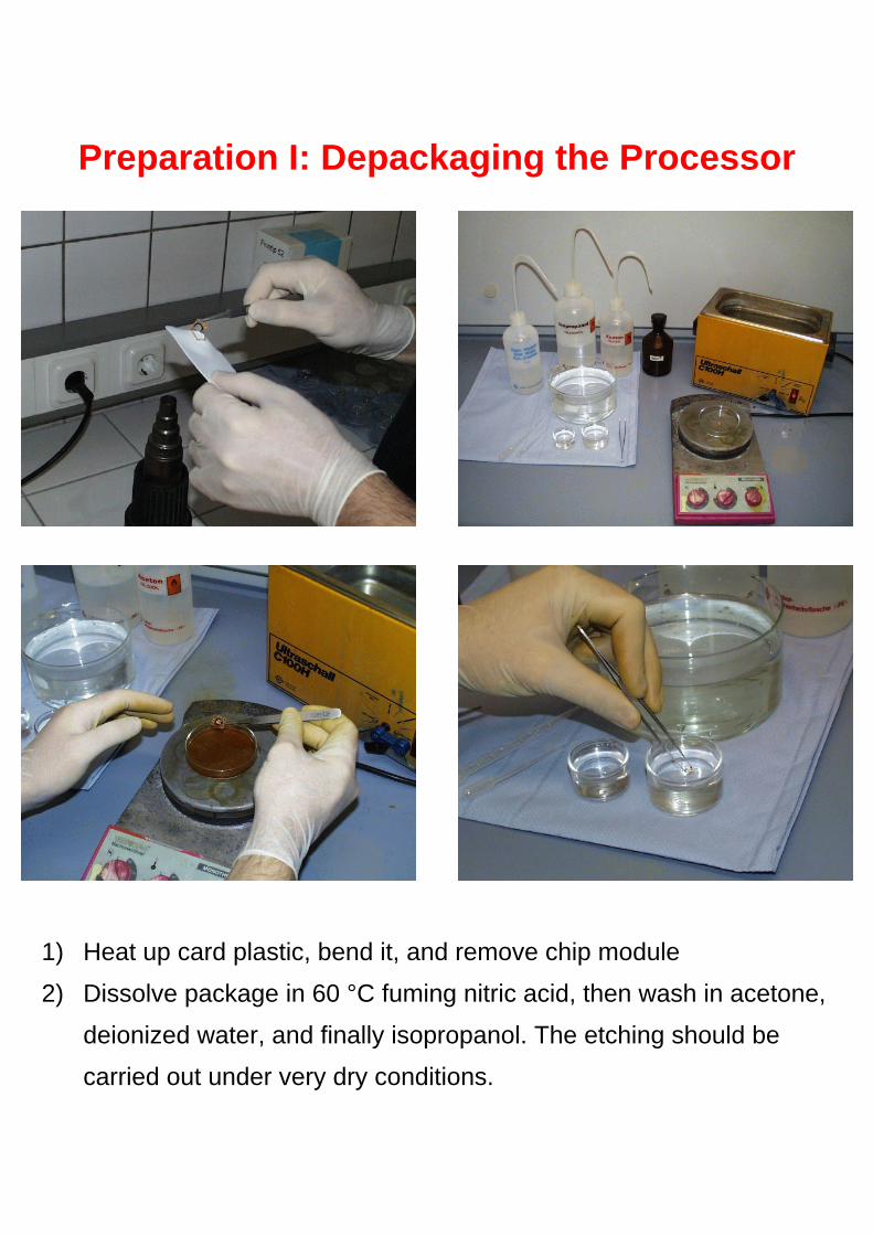
1)
2)
Heat up card plastic, bend it, and remove chip module
Dissolve package in 60 °C fuming nitric acid, then wash in acetone,
deionized water, and finally isopropanol. The etching should be
carried out under very dry conditions.
Preparation I: Depackaging the Processor
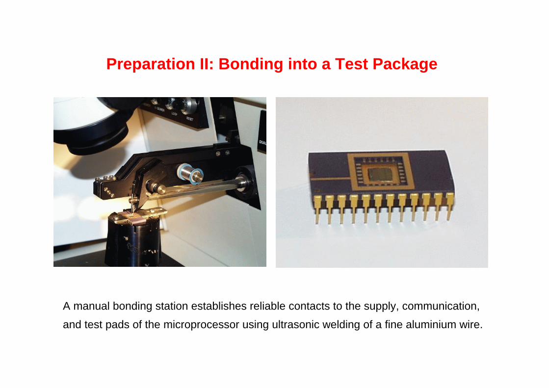
A manual bonding station establishes reliable contacts to the supply, communication,
Preparation II: Bonding into a Test Package
and test pads of the microprocessor using ultrasonic welding of a fine aluminium wire.
A B
A B
BVCC A A B
VCC
GND
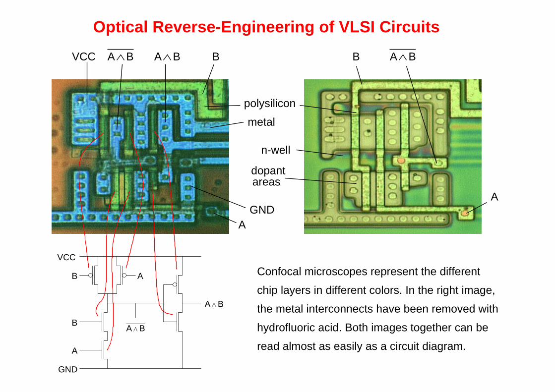
Confocal microscopes represent the different
the metal interconnects have been removed with
hydrofluoric acid. Both images together can be
A B B
A
metal
polysilicon
AGND
B
B A
areasdopant
n-well
chip layers in different colors. In the right image,
read almost as easily as a circuit diagram.
Optical Reverse-Engineering of VLSI Circuits
B
A
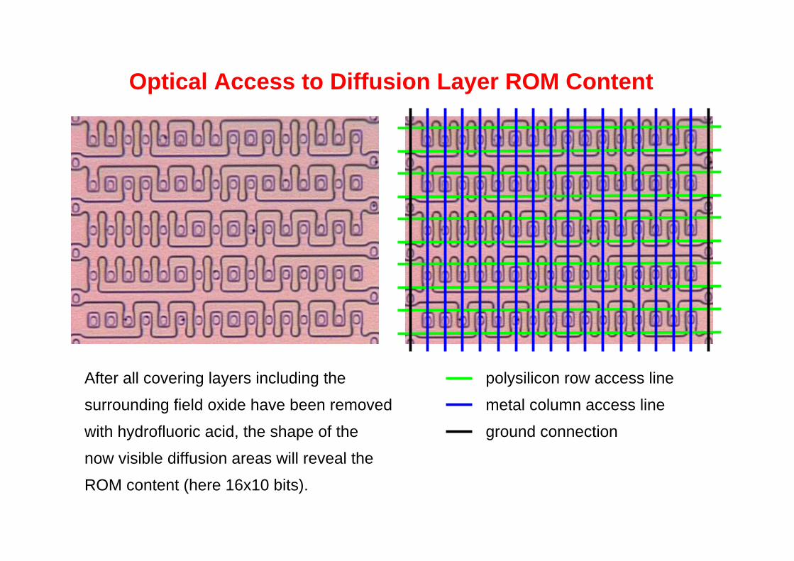
After all covering layers including the
surrounding field oxide have been removed
with hydrofluoric acid, the shape of the ground connection
metal column access line
polysilicon row access line
Optical Access to Diffusion Layer ROM Content
now visible diffusion areas will reveal the
ROM content (here 16x10 bits).
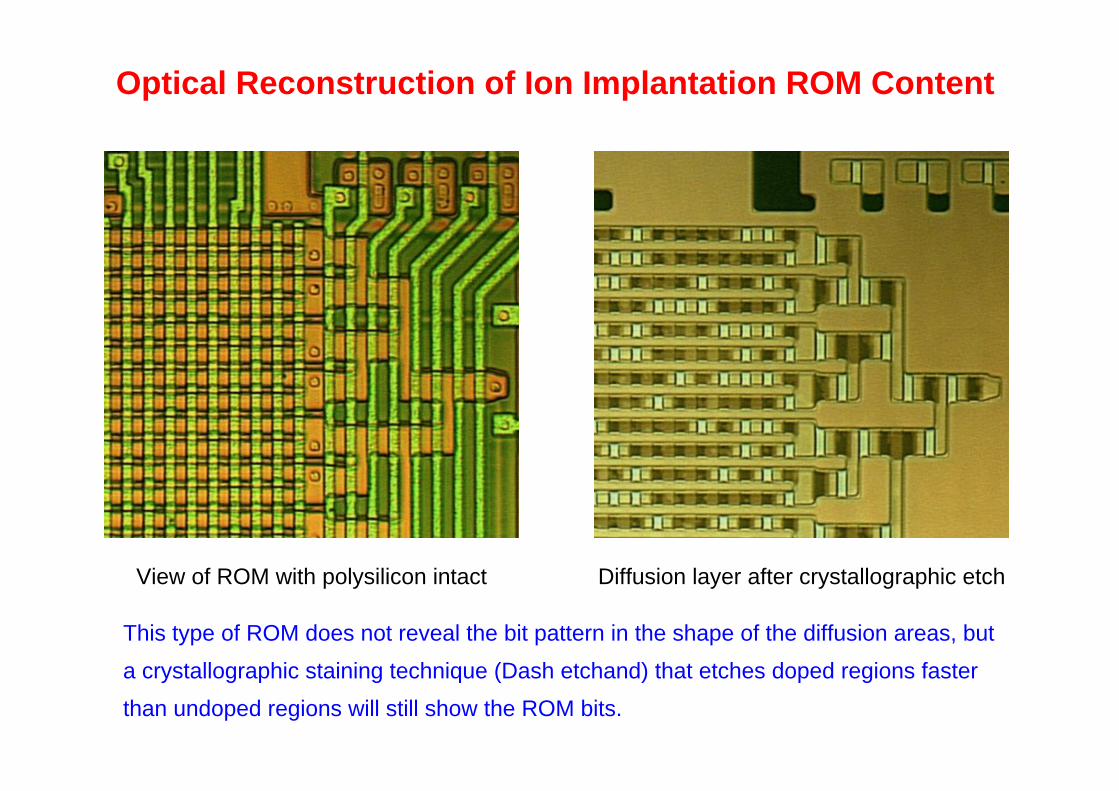
Optical Reconstruction of Ion Implantation ROM Content
View of ROM with polysilicon intact Diffusion layer after crystallographic etch
This type of ROM does not reveal the bit pattern in the shape of the diffusion areas, but
a crystallographic staining technique (Dash etchand) that etches doped regions faster
than undoped regions will still show the ROM bits.

acquisition, oscilloscope, pattern generator, power supply,
Access to CPU Bus via Laser Depassivation and Microprobing
Photos: ADSR
DSP card for card protocol interface handling and data
Top: A complete microprobing station consisting of a micro-
scope (Mitutoyo FS-60), laser cutter (New Wave QuikLaze),
logic analyzer, etc. Right: Eight depassivated data bus lines.
four micropositioners (Karl Suss), CCD camera, PC with
to attack all applications. Carefully designed smartcard software makes it difficult
Options:
Disable instruction decoder, such that no JMP/CALL/RET/HALT instructions
Passively monitoring and recording all memory-bus accesses might not be sufficient
to trigger memory accesses to all secrets in a laboratory.
Microprobing Access to All Memory Locations
Card software that calculates a full memory checksum after each reset
simplifies attacks considerably!
Solution for Attacker:
Abuse existing processor hardware as an address generator that accesses
all memory locations predictably. A single probing needle can now capture
all memory values, probing one bus line at a time.
are executed (preferably only NOP-like instructions should be allowed).
Disable program-counter load gate
In many smartcard processors, this can be accomplished with just a single probe!

Focused Ion Beam Workstations for IC Modification
0.01 µm resolution. Gallium ions are accelerated
with 30 kV and process gases like iodine or an organic
Left Photo: Dept. of Material Sciences, University of Cambridge
Focused ion-beam machines make high-resolution
compound are injected near the target location.
images of chip structures and allow us to both remove
and deposit materials (metal and insulators) with

Electron Beam Testing
Modified scanning electron microscope (SEM) with voltage contrast function.
Primary electrons (2.5 kV, 5 nA) hit secondary electrons out of the target location.
Limitation:
Measured signal is the low-pass filtered product of the beam current multiplied
Stroboscopic measurements allow to capture periodic signals with
a bandwidth of several gigahertz
limited to a few megahertz
Real-time voltage contrast observation of a non-periodic signal is
This allows contact-free signal measurements on the chip.
indicates local field potential.
Number and energy of secondary electrons recorded by spectrometer and detector
with a function of the signal voltage.
Analog Circuit Characteristics Allow Non-Invasive Attacks
Delays vary along various signal paths (RC and gate count)
Static current consumption extremely small
Significant short-circuit when SRAM cell changes state
Brief short-circuit when CMOS gate changes state
Flip-flop metastability
Flip-flops sample input during a short interval and compare it with the
supply voltage levels.
Smartcards are particularly vulnerable to non-invasive attacks because the attacker
simulations. Smartcard security cannot be achieved by studying
only a digital abstraction of the processor design.
Careful security reviews must usually include detailed analog VLSI
... plus many other physical and electronic effects ...
has full control over power and clock supply lines and environmental conditions.
Capacitive loads draw current when a gate changes state
����������������������������������������������������������������
����������������������������������������������������������������
����������������
����������������
������������
������������
R
C
VCC
CLK
PROBE
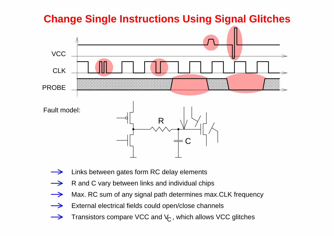
Change Single Instructions Using Signal Glitches
Fault model:
Links between gates form RC delay elements
R and C vary between links and individual chips
Max. RC sum of any signal path determines max.CLK frequency
External electrical fields could open/close channels
Transistors compare VCC and V , which allows VCC glitchesC
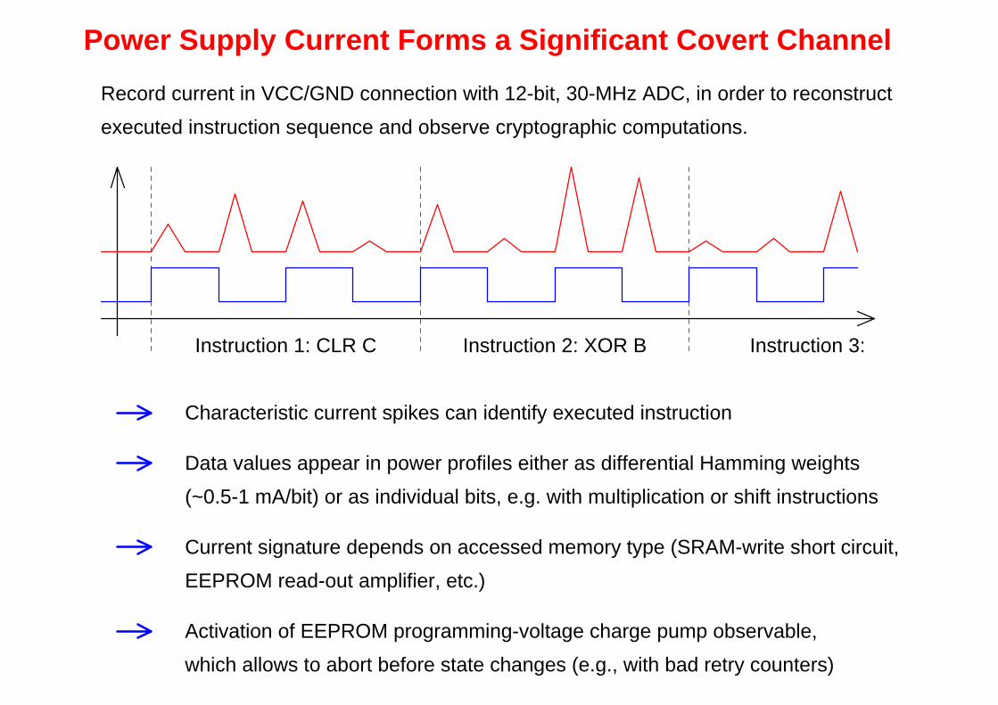
Instruction 1: CLR C Instruction 2: XOR B Instruction 3:
Data values appear in power profiles either as differential Hamming weights
Activation of EEPROM programming-voltage charge pump observable,
which allows to abort before state changes (e.g., with bad retry counters)
(~0.5-1 mA/bit) or as individual bits, e.g. with multiplication or shift instructions
Characteristic current spikes can identify executed instruction
EEPROM read-out amplifier, etc.)
Power Supply Current Forms a Significant Covert Channel
executed instruction sequence and observe cryptographic computations.
Record current in VCC/GND connection with 12-bit, 30-MHz ADC, in order to reconstruct
Current signature depends on accessed memory type (SRAM-write short circuit,
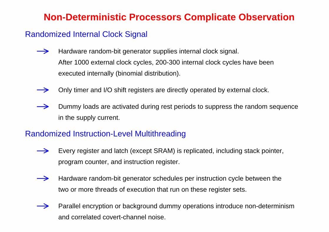
After 1000 external clock cycles, 200-300 internal clock cycles have been
executed internally (binomial distribution).
Randomized Internal Clock Signal
Only timer and I/O shift registers are directly operated by external clock.
Randomized Instruction-Level Multithreading
program counter, and instruction register.
Parallel encryption or background dummy operations introduce non-determinism
Dummy loads are activated during rest periods to suppress the random sequence
in the supply current.
Every register and latch (except SRAM) is replicated, including stack pointer,
Hardware random-bit generator schedules per instruction cycle between the
Non-Deterministic Processors Complicate Observation
Hardware random-bit generator supplies internal clock signal.
two or more threads of execution that run on these register sets.
and correlated covert-channel noise.
:4D
Q
Q
QS
R
RST
CLK
Bus
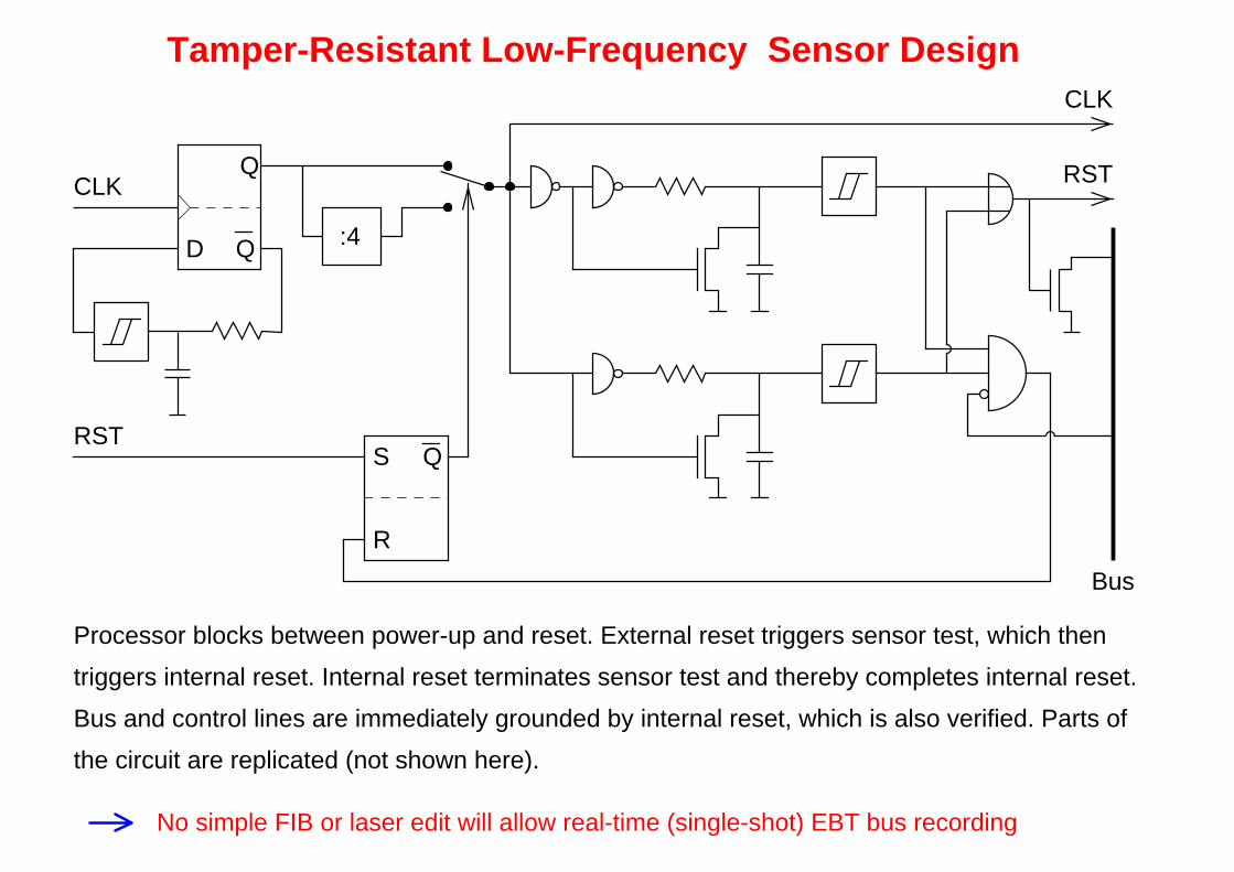
Tamper-Resistant Low-Frequency Sensor Design
Processor blocks between power-up and reset. External reset triggers sensor test, which then
CLK
RST
triggers internal reset. Internal reset terminates sensor test and thereby completes internal reset.
Bus and control lines are immediately grounded by internal reset, which is also verified. Parts of
the circuit are replicated (not shown here).
No simple FIB or laser edit will allow real-time (single-shot) EBT bus recording
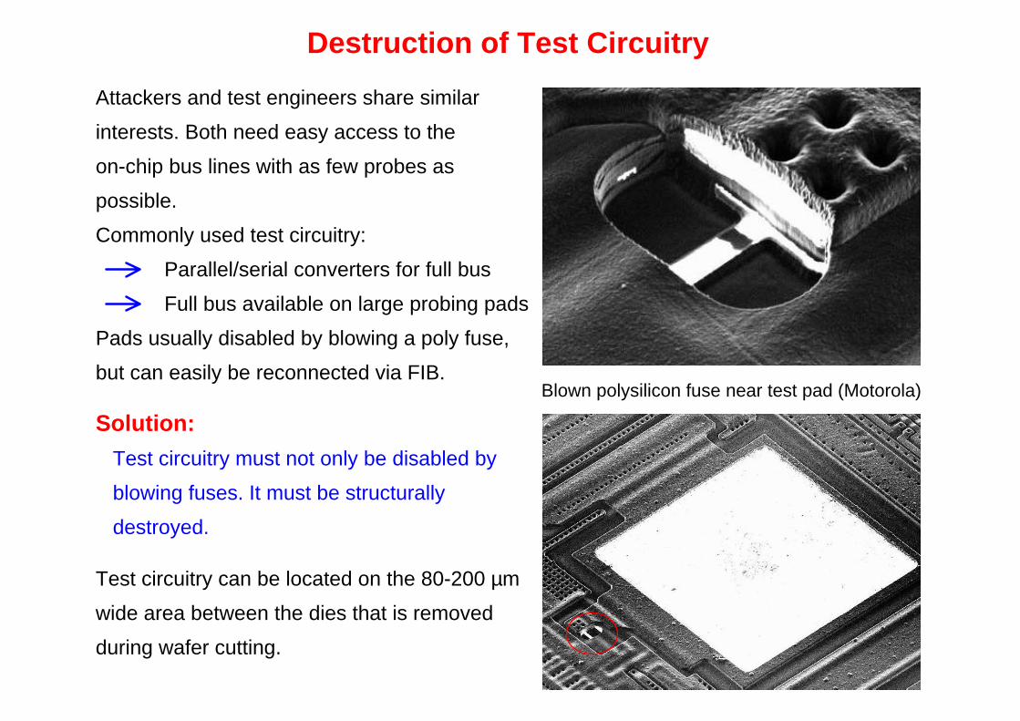
Attackers and test engineers share similar
interests. Both need easy access to the
Blown polysilicon fuse near test pad (Motorola)
possible.
Full bus available on large probing pads
Solution:
Test circuitry must not only be disabled by
blowing fuses. It must be structurally
destroyed.
Test circuitry can be located on the 80-200 µm
wide area between the dies that is removed
during wafer cutting.
Pads usually disabled by blowing a poly fuse,
but can easily be reconnected via FIB.
on-chip bus lines with as few probes as
Parallel/serial converters for full bus
Commonly used test circuitry:
Destruction of Test Circuitry
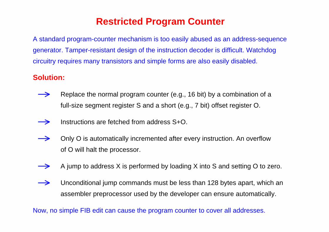
Restricted Program Counter
Solution:
full-size segment register S and a short (e.g., 7 bit) offset register O.
Instructions are fetched from address S+O.
A jump to address X is performed by loading X into S and setting O to zero.
assembler preprocessor used by the developer can ensure automatically.
Now, no simple FIB edit can cause the program counter to cover all addresses.
circuitry requires many transistors and simple forms are also easily disabled.
Only O is automatically incremented after every instruction. An overflow
Replace the normal program counter (e.g., 16 bit) by a combination of a
Unconditional jump commands must be less than 128 bytes apart, which an
generator. Tamper-resistant design of the instruction decoder is difficult. Watchdog
A standard program-counter mechanism is too easily abused as an address-sequence
of O will halt the processor.
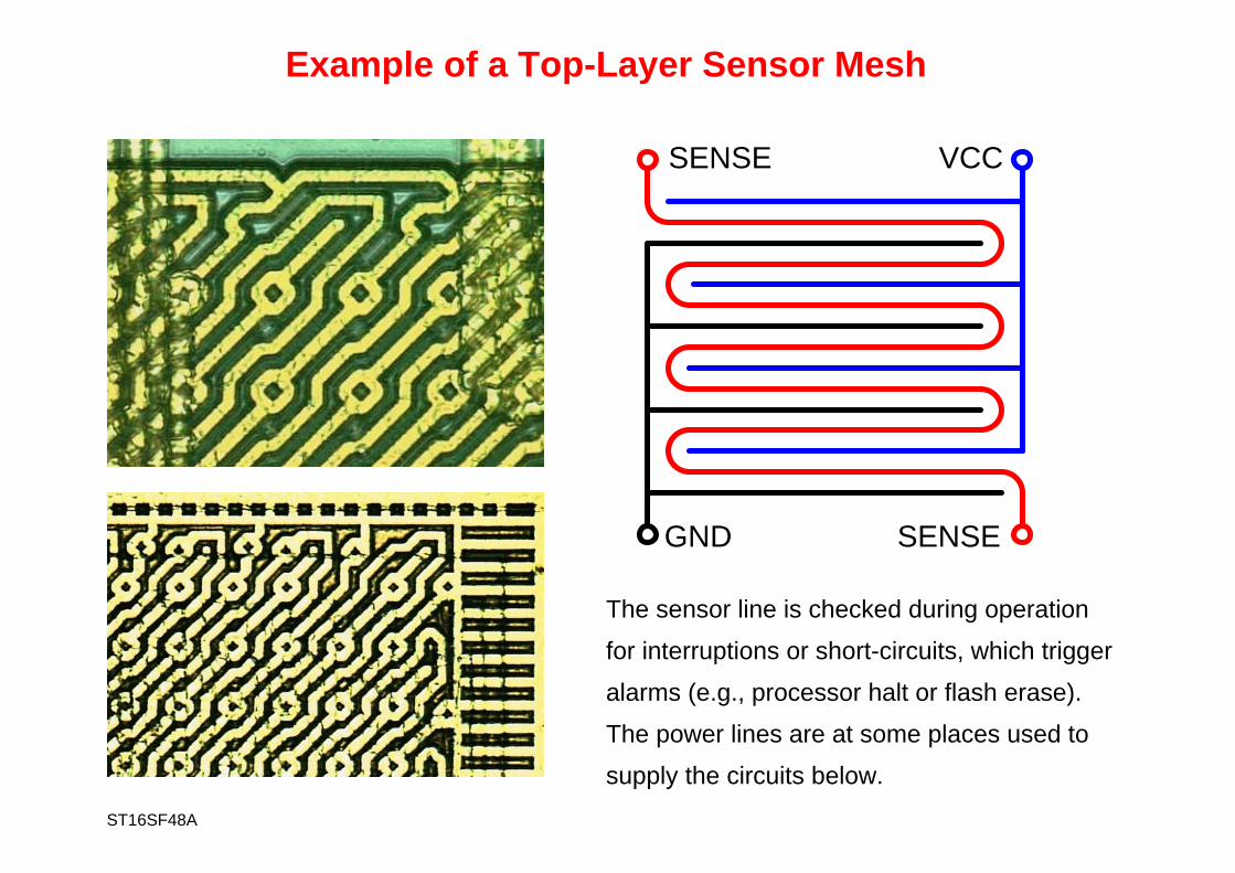
SENSE
VCC
GND
SENSE
The sensor line is checked during operation
for interruptions or short-circuits, which trigger
alarms (e.g., processor halt or flash erase).
The power lines are at some places used to
supply the circuits below.
ST16SF48A
Example of a Top-Layer Sensor Mesh
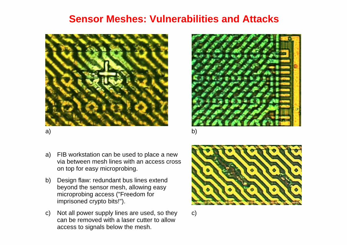
a) b)
a)
on top for easy microprobing.
b)
c)can be removed with a laser cutter to allowaccess to signals below the mesh.
imprisoned crypto bits!").
Not all power supply lines are used, so they
Sensor Meshes: Vulnerabilities and Attacks
via between mesh lines with an access crossFIB workstation can be used to place a new
Design flaw: redundant bus lines extendbeyond the sensor mesh, allowing easymicroprobing access ("Freedom for
c)
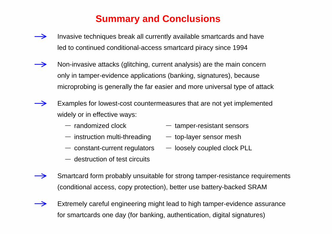
Invasive techniques break all currently available smartcards and have
led to continued conditional-access smartcard piracy since 1994
tamper-resistant sensors
top-layer sensor mesh
Examples for lowest-cost countermeasures that are not yet implemented
(conditional access, copy protection), better use battery-backed SRAM
randomized clock
instruction multi-threading
constant-current regulators
destruction of test circuits
microprobing is generally the far easier and more universal type of attack
loosely coupled clock PLL
Extremely careful engineering might lead to high tamper-evidence assurance
for smartcards one day (for banking, authentication, digital signatures)
widely or in effective ways:
Summary and Conclusions
only in tamper-evidence applications (banking, signatures), because
Non-invasive attacks (glitching, current analysis) are the main concern
Smartcard form probably unsuitable for strong tamper-resistance requirements