Embed Size (px)
Citation preview

Design of an Instrumentation Amplifier
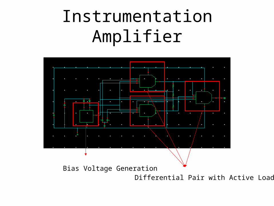
Instrumentation Amplifier
Differential Pair with Active LoadBias Voltage Generation
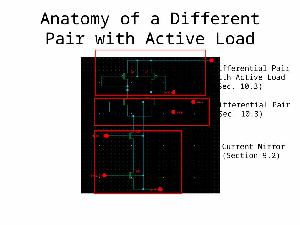
Anatomy of a Different Pair with Active Load
Differential Pair (Sec. 10.3)
Differential Pair with Active Load(Sec. 10.3)
Current Mirror (Section 9.2)

Bias Voltage Generation
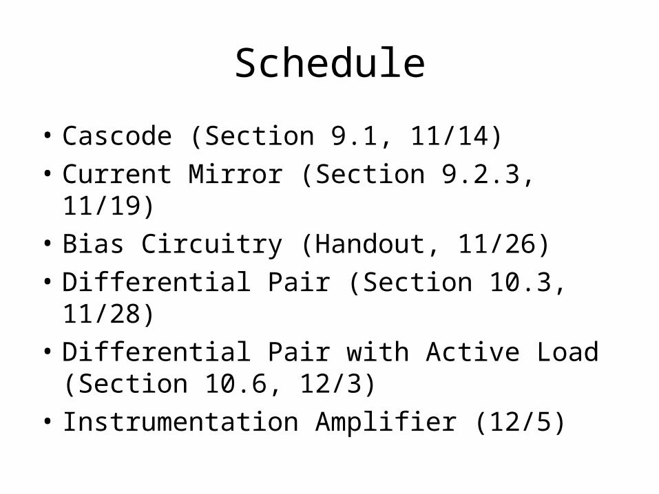
Schedule
• Cascode (Section 9.1, 11/14)• Current Mirror (Section 9.2.3, 11/19)• Bias Circuitry (Handout, 11/26)• Differential Pair (Section 10.3, 11/28)• Differential Pair with Active Load
(Section 10.6, 12/3)• Instrumentation Amplifier (12/5)
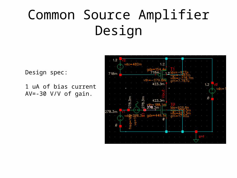
Common Source Amplifier Design
Design spec:
1 uA of bias currentAV=-30 V/V of gain.
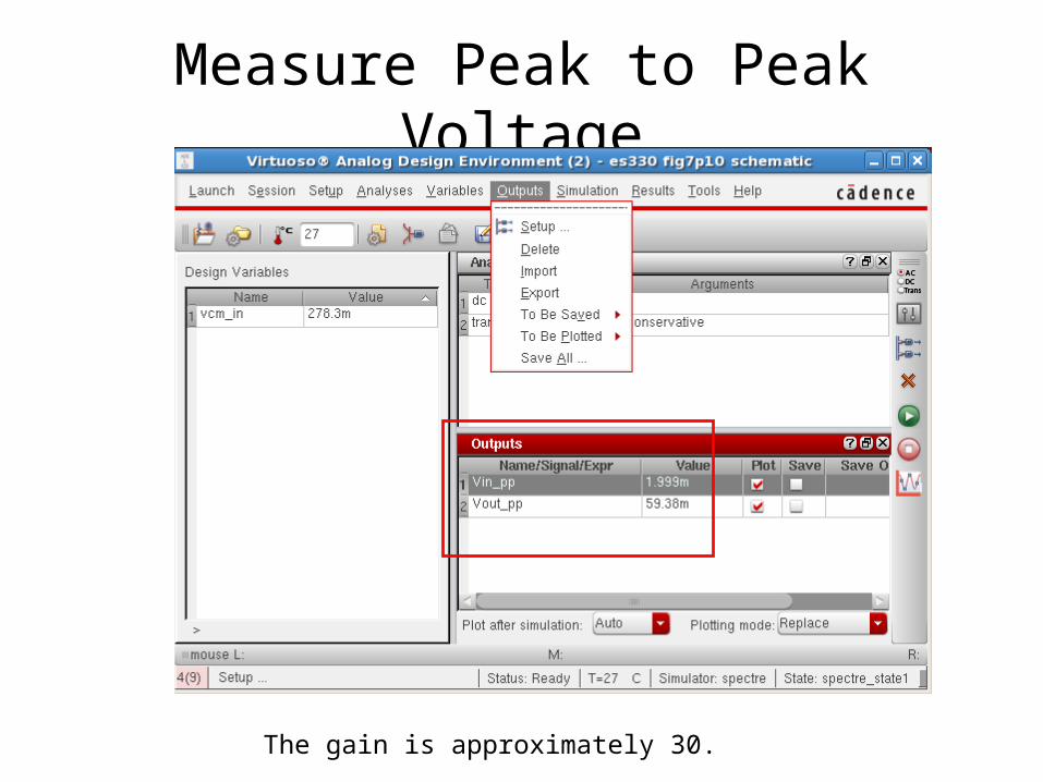
Measure Peak to Peak Voltage
The gain is approximately 30.
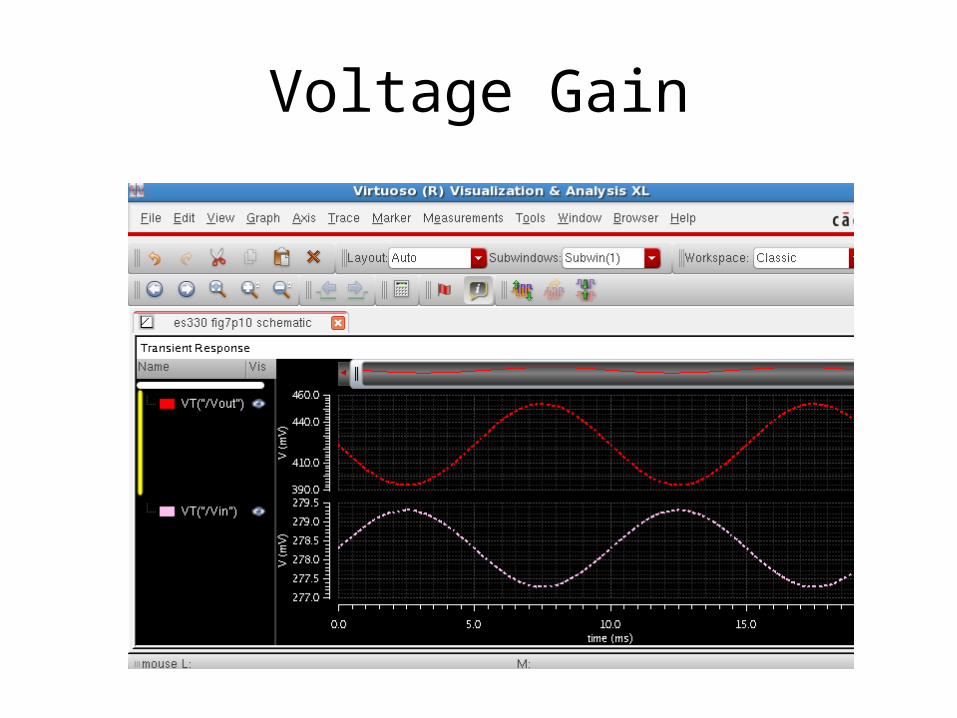
Voltage Gain

Design Exploration
• Initial results– ro1=2.228 Mohms– ro2=5.32 Mohms– Av=-31.4 V/V– gmovergds1=44.57– gmvoergds2=42.5
Design: If we can increase ro1, we can potentially raise the gain!
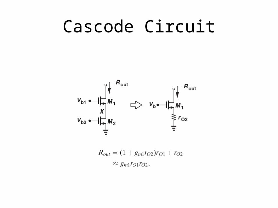
Cascode Circuit
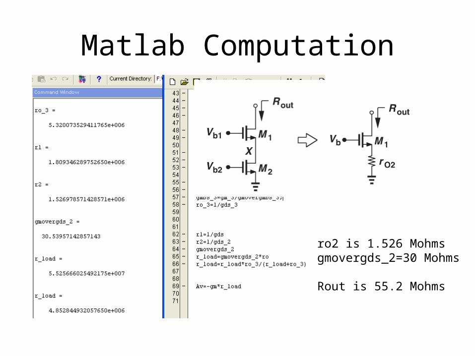
Matlab Computation
ro2 is 1.526 Mohmsgmovergds_2=30 Mohms
Rout is 55.2 Mohms
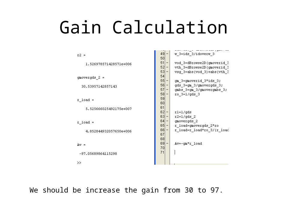
Gain Calculation
We should be increase the gain from 30 to 97.
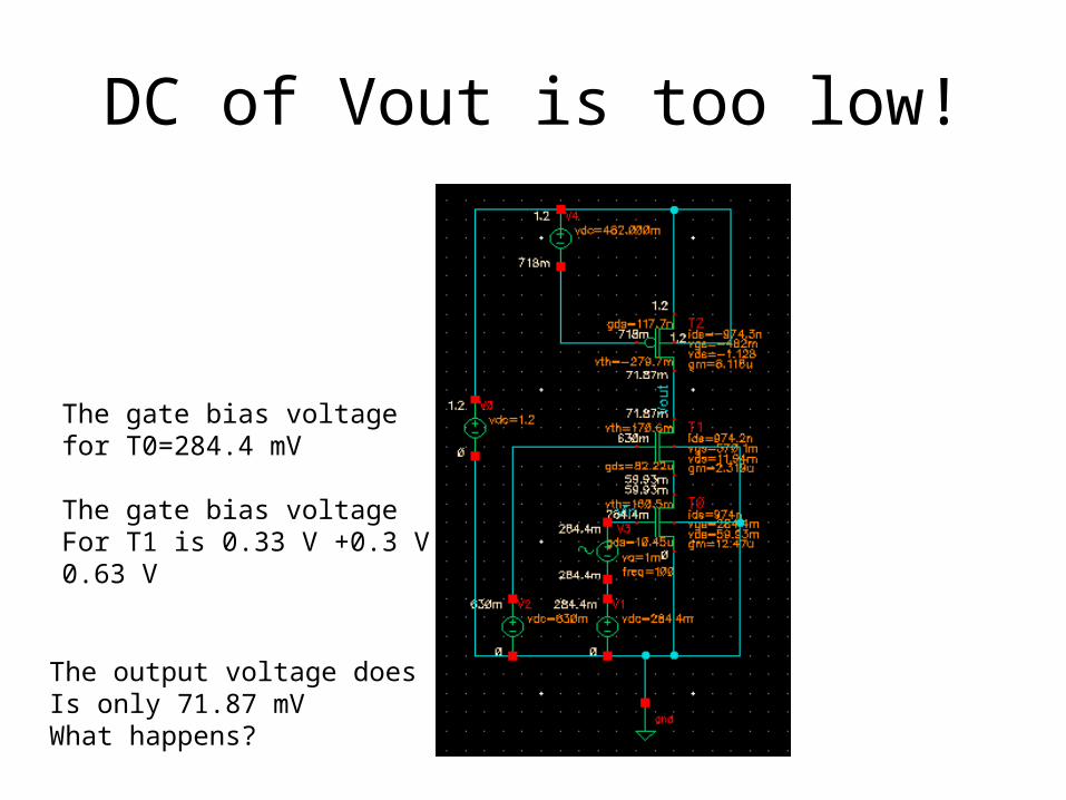
DC of Vout is too low!
The gate bias voltage for T0=284.4 mV
The gate bias voltageFor T1 is 0.33 V +0.3 V0.63 V
The output voltage doesIs only 71.87 mV What happens?
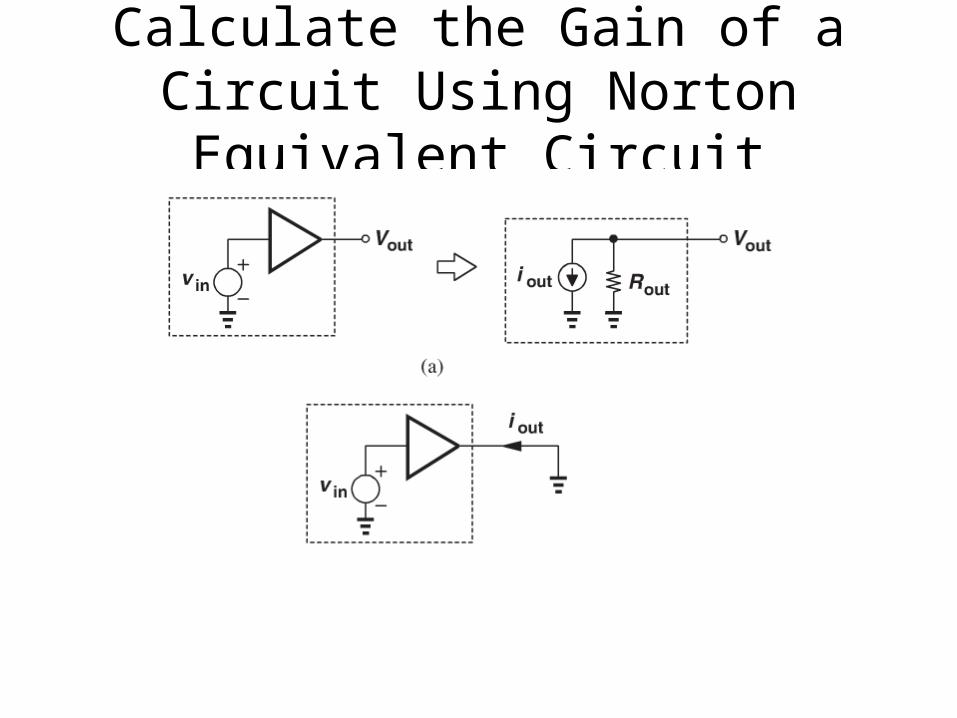
Calculate the Gain of a Circuit Using Norton Equivalent Circuit
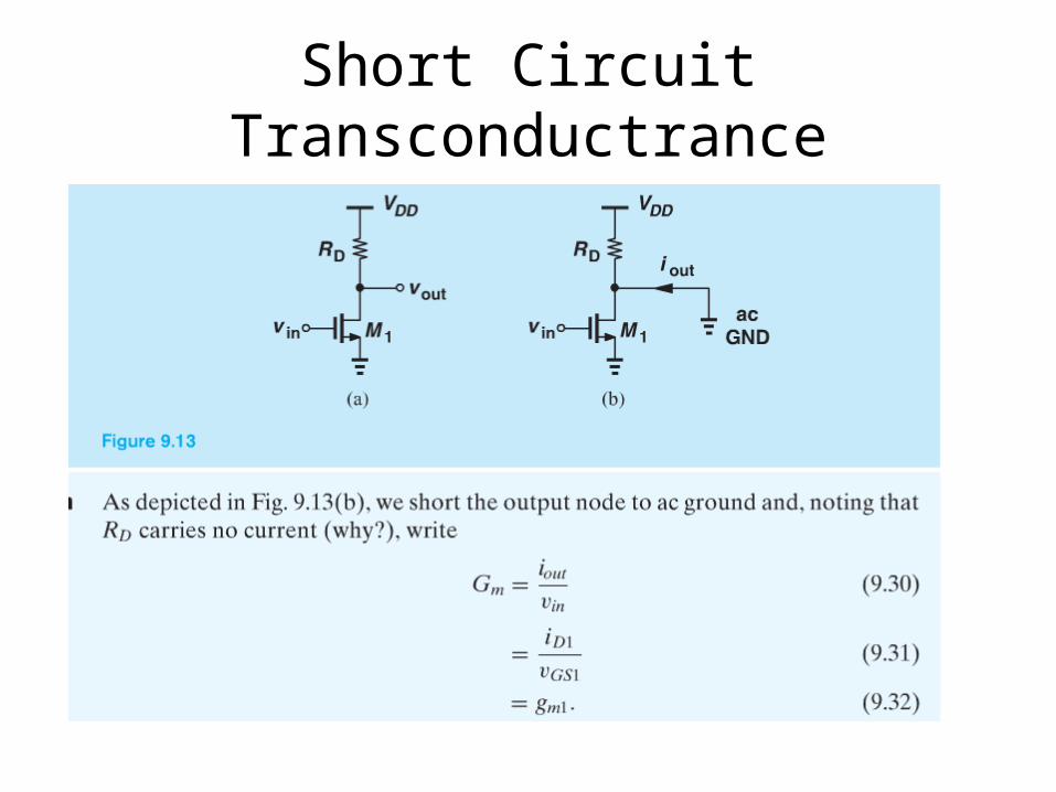
Short Circuit Transconductrance
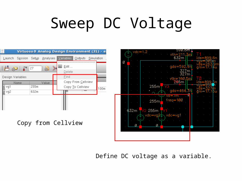
Sweep DC Voltage
Define DC voltage as a variable.
Copy from Cellview

Setup the Sweep
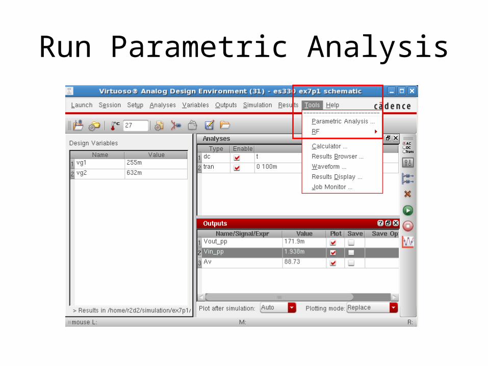
Run Parametric Analysis
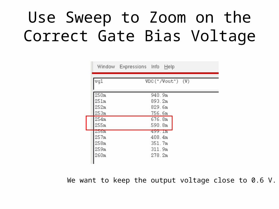
Use Sweep to Zoom on the Correct Gate Bias Voltage
We want to keep the output voltage close to 0.6 V.
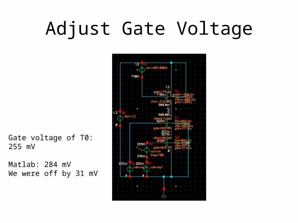
Adjust Gate Voltage
Gate voltage of T0:255 mV
Matlab: 284 mVWe were off by 31 mV
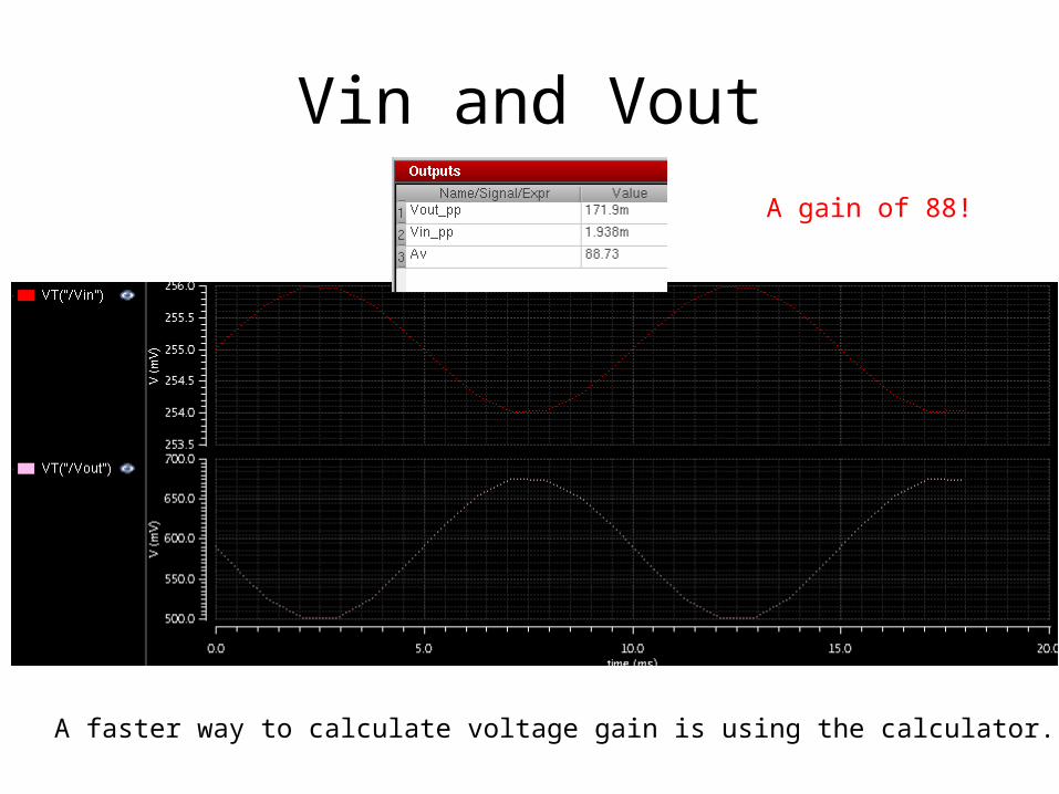
Vin and Vout
A faster way to calculate voltage gain is using the calculator.
A gain of 88!

Using the Calculator
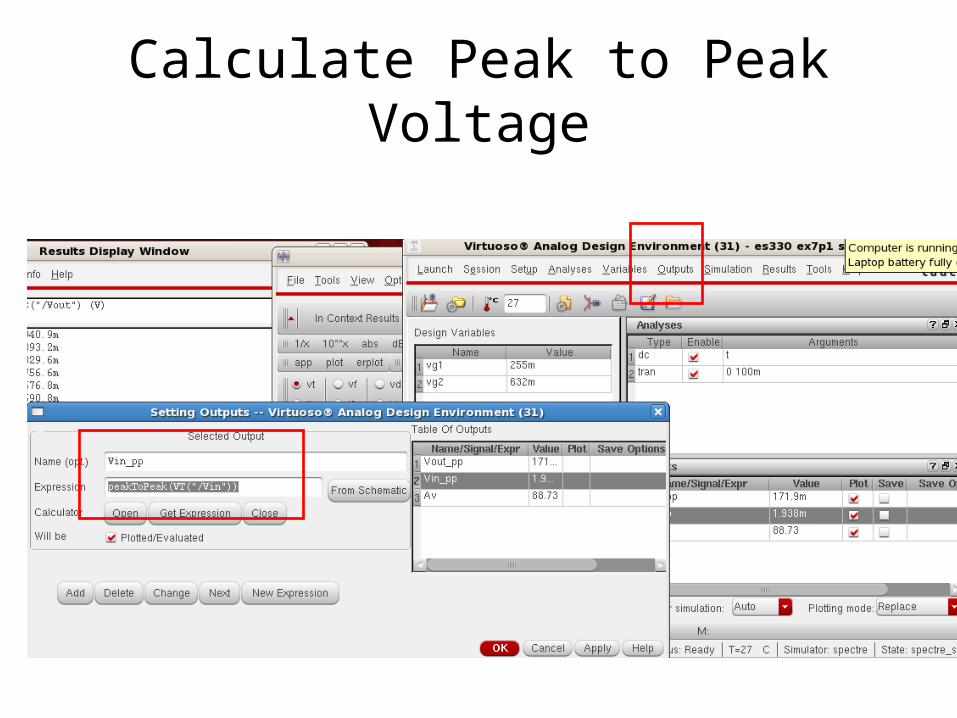
Calculate Peak to Peak Voltage