Embed Size (px)
Citation preview
AP9214L Document number: DS38413 Rev. 2 - 2
1 of 17 www.diodes.com
April 2018 © Diodes Incorporated
AP9214L
NE
W P
RO
DU
CT
SINGLE CHIP SOLUTION FOR 1-CELL Li+ BATTERY PACK
Description
The AP9214L is a single chip protection solution specially designed
for 1-cell Li+ rechargeable battery pack application.
The AP9214L includes a 1-cell Lion battery protection chip and dual
N-CH, ultra low RSS(ON) MOSFET with common drain.
The AP9214L provides rich battery protection features and can turn-
off the N-CH MOSFET by detecting overcharge voltage/current, over
discharge voltage/current, or load short circuit. The AP9214L has
built-in fixed delay time to save external components.
The AP9214L is available in U-DFN2535-6 package with two kinds of
pin options.
Features
High Voltage CMOS Process, up to 30V (VDD to VM)
Low Quiescent Current (+25°C )
In Normal Mode, 3.0µA (Typ.), 4.5µA (Max.), VDD = 3.5V
In Power-Down Mode, 0.1µA (Max.)
High-Accuracy Voltage Detection Circuit (+25°C)
Overcharge Detection Voltage: 3.5V to 4.5V (5mV Steps)
Accuracy ±25mV
Overcharge Hysteresis Voltage Range: 0.1V to 0.4V (50mV
Steps) Accuracy ±50mV
Overdischarge Detection Voltage: 2.0V to 3.4V (10mV
Steps) Accuracy ±35mV
Overdischarge Hysteresis Voltage Range: 0V to 0.7V (40mV
Steps) Accuracy ±65mV
Discharge Overcurrent Detection Voltage: 0.05V to 0.32V
(10mV Steps) Accuracy ±15mV
Short Current Detection Voltage: 0.45V to 0.7V (50mV
Steps) Accuracy ±100mV
Charge Overcurrent Detection Voltage: -0.2V to -0.05V
(10mV Steps) Accuracy ±15mV
Overcharger Detection Voltage: 8.0V (Fixed) Accuracy ±2V
Overcharger Release Voltage: 7.3V (Fixed) Accuracy ±2V
Built-in Fixed Detection Delay Time (+25°C), Accuracy ±20%
Power-Down Mode Selectable (Yes or No)
0V Battery Charge Selectable (Permission or Inhibition)
Overcharge Protection Mode Selectable (Auto Release or
Latch)
Totally Lead-Free & Fully RoHS Compliant (Notes 1 & 2)
Halogen and Antimony Free. “Green” Device (Note 3)
Pin Assignments
(Top View)
1
2
3
5
4
S1
VSS
VDD
NC
S2
VM
6
EP
U-DFN2535-6 (Option 1)
1
2
3
5
4
S1
VSS
VDD
VM
S2
NC
6
EP
U-DFN2535-6 (Option 2)
Applications
Li+ Rechargeable Battery Pack
Notes: 1. No purposely added lead. Fully EU Directive 2002/95/EC (RoHS), 2011/65/EU (RoHS 2) & 2015/863/EU (RoHS 3) compliant. 2. See https://www.diodes.com/quality/lead-free/ for more information about Diodes Incorporated’s definitions of Halogen- and Antimony-free, "Green" and Lead-free.
3. Halogen- and Antimony-free "Green” products are defined as those which contain <900ppm bromine, <900ppm chlorine (<1500ppm total Br + Cl) and
<1000ppm antimony compounds.
AP9214L Document number: DS38413 Rev. 2 - 2
2 of 17 www.diodes.com
April 2018 © Diodes Incorporated
AP9214L
NE
W P
RO
DU
CT
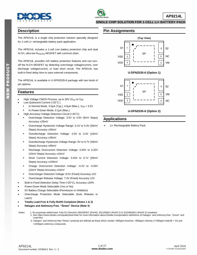
Typical Applications Circuit (Note 4)
U1
AP9214L
(U-DFN2535-6)BAT
P+
C1
100n
R2
2.7kΩ
P-
VDD
VSS S1 S2
VM
1(1)
2(2)
3(3)4(5)
6(6)
R1
330Ω to 470Ω
Note: 4. R1 and C1 are used to stabilize the supply voltage of the AP9214L. The recommended range of R1 value is 330Ω to 470Ω and C1 value is 10nF to
1000nF, typical value is 100nF. R2 should be connected between P- to VM sense terminal to monitor the status of charger and the charge/discharge
current. The R2 should be between 300Ω and 4kΩ, typical value is 2.7kΩ. R1 and R2 are also used as current limit resistors if the battery or charger is
connected reversely. Polarity reversing may cause the power consumption of R1 and R2 to go over their power dissipation rating, therefore R1 and R2
values should be selected appropriately for the actual application. If R2 is more than 4kΩ resistor, charge may not be off due to the voltage drop on R2.
For power-down mode, when first connecting AP9214L system board to the battery, it is necessary to use charger or to short P- to the battery negative
polarity. Once the AP9214L is activated, the charger or connection can be removed, otherwise the battery cannot discharge current through system
board.
The values selected should follow the recommended typical range mentioned above. It has not been confirmed whether the operation is normal or not in
circuits other than the above example of connection. In addition, the example of connection shown above and the typical value do not exactly guarantee
proper operation. Please perform the actual application to set the suitable value through your complete evaluation.
Pin Descriptions
Pin Number
Option 1
Pin Number
Option 2 Pin Name Function
1 1 S1 Source pin of discharging MOSFET, connecting this pin to battery negative pole.
2 2 VSS Negative power supply pin.
3 3 VDD Positive power supply pin, connecting this pin to battery positive pole through R1.
4 5 VM Charger negative input pin, short this pin to S2 pin through R2.
5 4 NC Not connected, leave this pin floating.
6 6 S2 Source pin of charging MOSFET, connecting this pin to charge negative input.
EP EP Drain Thermal PAD is common drain of charge and discharge MOSFET, so in PCB layout, prefer to
use large copper area to cover this pad for better thermal dissipation, then leave it open.
A (B) A for Pin-out Option 1 B for Pin-out Option 2
AP9214L Document number: DS38413 Rev. 2 - 2
3 of 17 www.diodes.com
April 2018 © Diodes Incorporated
AP9214L
NE
W P
RO
DU
CT
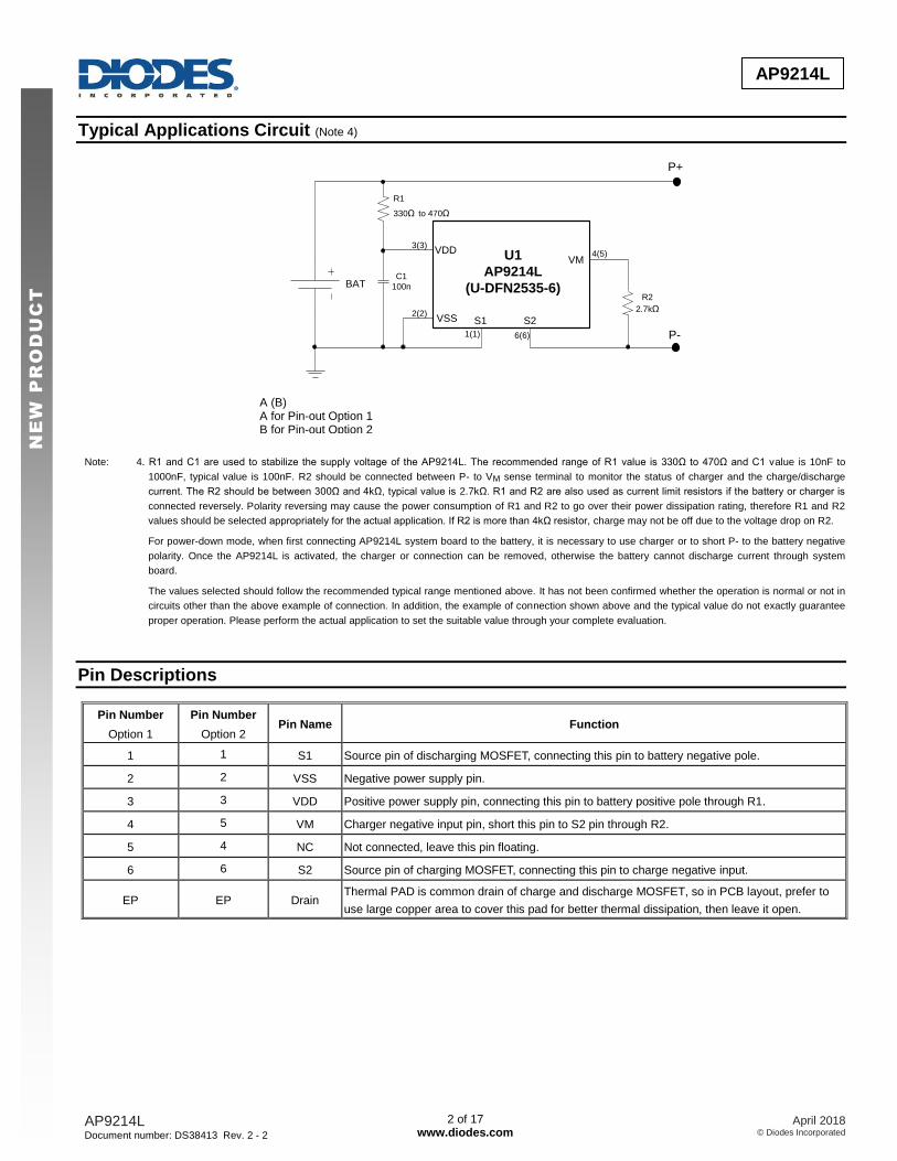
Functional Block Diagram
Logic Circuit
Logic Circuit
Delay Time
Circuit
0 V
Charge
Option
Level Shift
RVMD
RVMS
S1 S2D2D1
G1 G2
VDD
VSS
S2S1
VM
Drain
EP
4 (5)
1(1) 6(6)
2 (2)
3 (3)
A (B) A for Pin-out Option 1 B for Pin-out Option 2
AP9214L Document number: DS38413 Rev. 2 - 2
4 of 17 www.diodes.com
April 2018 © Diodes Incorporated
AP9214L
NE
W P
RO
DU
CT
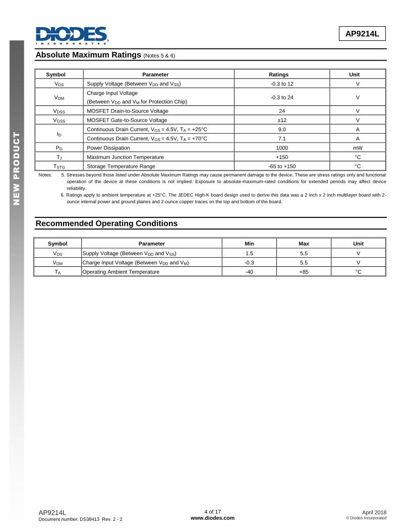
Absolute Maximum Ratings (Notes 5 & 6)
Symbol Parameter Ratings Unit
VDS Supply Voltage (Between VDD and VSS) -0.3 to 12 V
VDM Charge Input Voltage
(Between VDD and VM for Protection Chip) -0.3 to 24 V
VDSS MOSFET Drain-to-Source Voltage 24 V
VGSS MOSFET Gate-to-Source Voltage ±12 V
ID Continuous Drain Current, VGS = 4.5V, TA = +25°C 9.0 A
Continuous Drain Current, VGS = 4.5V, TA = +70°C 7.1 A
PD Power Dissipation 1000 mW
TJ Maximum Junction Temperature +150 °C
TSTG Storage Temperature Range -65 to +150 °C
Notes: 5. Stresses beyond those listed under Absolute Maximum Ratings may cause permanent damage to the device. These are stress ratings only and functional
operation of the device at these conditions is not implied. Exposure to absolute-maximum-rated conditions for extended periods may affect device
reliability.
6. Ratings apply to ambient temperature at +25°C. The JEDEC High-K board design used to derive this data was a 2 inch x 2 inch multilayer board with 2-
ounce internal power and ground planes and 2-ounce copper traces on the top and bottom of the board.
Recommended Operating Conditions
Symbol Parameter Min Max Unit
VDS Supply Voltage (Between VDD and VSS) 1.5 5.5 V
VDM Charge Input Voltage (Between VDD and VM) -0.3 5.5 V
TA Operating Ambient Temperature -40 +85 °C
AP9214L Document number: DS38413 Rev. 2 - 2
5 of 17 www.diodes.com
April 2018 © Diodes Incorporated
AP9214L
NE
W P
RO
DU
CT
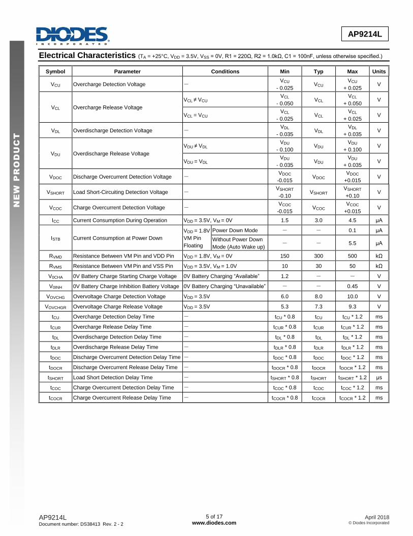
Electrical Characteristics (TA = +25°C, VDD = 3.5V, VSS = 0V, R1 = 220Ω, R2 = 1.0kΩ, C1 = 100nF, unless otherwise specified.)
Symbol Parameter Conditions Min Typ Max Units
VCU Overcharge Detection Voltage - VCU
- 0.025 VCU
VCU
+ 0.025 V
VCL Overcharge Release Voltage
VCL ≠ VCU VCL
- 0.050 VCL
VCL
+ 0.050 V
VCL = VCU VCL
- 0.025 VCL
VCL
+ 0.025 V
VDL Overdischarge Detection Voltage - VDL
- 0.035 VDL
VDL
+ 0.035 V
VDU Overdischarge Release Voltage
VDU ≠ VDL VDU
- 0.100 VDU
VDU
+ 0.100 V
VDU = VDL VDU
- 0.035 VDU
VDU
+ 0.035 V
VDOC Discharge Overcurrent Detection Voltage - VDOC
-0.015 VDOC
VDOC
+0.015 V
VSHORT Load Short-Circuiting Detection Voltage - VSHORT
-0.10 VSHORT
VSHORT
+0.10 V
VCOC Charge Overcurrent Detection Voltage - VCOC
-0.015 VCOC
VCOC
+0.015 V
ICC Current Consumption During Operation VDD = 3.5V, VM = 0V 1.5 3.0 4.5 μA
ISTB Current Consumption at Power Down
VDD = 1.8V
VM Pin
Floating
Power Down Mode - - 0.1 μA
Without Power Down
Mode (Auto Wake up) - - 5.5 μA
RVMD Resistance Between VM Pin and VDD Pin VDD = 1.8V, VM = 0V 150 300 500 kΩ
RVMS Resistance Between VM Pin and VSS Pin VDD = 3.5V, VM = 1.0V 10 30 50 kΩ
V0CHA 0V Battery Charge Starting Charge Voltage 0V Battery Charging “Available” 1.2 - - V
V0INH 0V Battery Charge Inhibition Battery Voltage 0V Battery Charging “Unavailable” - - 0.45 V
VOVCHG Overvoltage Charge Detection Voltage VDD = 3.5V 6.0 8.0 10.0 V
VOVCHGR Overvoltage Charge Release Voltage VDD = 3.5V 5.3 7.3 9.3 V
tCU Overcharge Detection Delay Time - tCU * 0.8 tCU tCU * 1.2 ms
tCUR Overcharge Release Delay Time - tCUR * 0.8 tCUR tCUR * 1.2 ms
tDL Overdischarge Detection Delay Time - tDL * 0.8 tDL tDL * 1.2 ms
tDLR Overdischarge Release Delay Time - tDLR * 0.8 tDLR tDLR * 1.2 ms
tDOC Discharge Overcurrent Detection Delay Time - tDOC * 0.8 tDOC tDOC * 1.2 ms
tDOCR Discharge Overcurrent Release Delay Time - tDOCR * 0.8 tDOCR tDOCR * 1.2 ms
tSHORT Load Short Detection Delay Time - tSHORT * 0.8 tSHORT tSHORT * 1.2 μs
tCOC Charge Overcurrent Detection Delay Time - tCOC * 0.8 tCOC tCOC * 1.2 ms
tCOCR Charge Overcurrent Release Delay Time - tCOCR * 0.8 tCOCR tCOCR * 1.2 ms
AP9214L Document number: DS38413 Rev. 2 - 2
6 of 17 www.diodes.com
April 2018 © Diodes Incorporated
AP9214L
NE
W P
RO
DU
CT
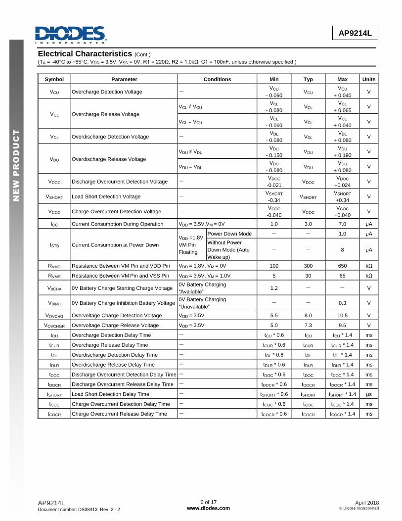
Electrical Characteristics (Cont.)
(TA = -40°C to +85°C, VDD = 3.5V, VSS = 0V, R1 = 220Ω, R2 = 1.0kΩ, C1 = 100nF, unless otherwise specified.)
Symbol Parameter Conditions Min Typ Max Units
VCU Overcharge Detection Voltage - VCU
- 0.060 VCU
VCU
+ 0.040 V
VCL Overcharge Release Voltage
VCL ≠ VCU VCL
- 0.080 VCL
VCL
+ 0.065 V
VCL = VCU VCL
- 0.060 VCL
VCL
+ 0.040 V
VDL Overdischarge Detection Voltage - VDL
- 0.080 VDL
VDL
+ 0.080 V
VDU Overdischarge Release Voltage
VDU ≠ VDL VDU
- 0.150 VDU
VDU
+ 0.190 V
VDU = VDL VDU
- 0.080 VDU
VDU
+ 0.080 V
VDOC Discharge Overcurrent Detection Voltage - VDOC
-0.021 VDOC
VDOC
+0.024 V
VSHORT Load Short Detection Voltage - VSHORT
-0.34 VSHORT
VSHORT
+0.34 V
VCOC Charge Overcurrent Detection Voltage - VCOC
-0.040 VCOC
VCOC
+0.040 V
ICC Current Consumption During Operation VDD = 3.5V,VM = 0V 1.0 3.0 7.0 μA
ISTB Current Consumption at Power Down
VDD =1.8V
VM Pin
Floating
Power Down Mode - - 1.0 μA
Without Power
Down Mode (Auto
Wake up)
- - 8 μA
RVMD Resistance Between VM Pin and VDD Pin VDD = 1.8V, VM = 0V 100 300 650 kΩ
RVMS Resistance Between VM Pin and VSS Pin VDD = 3.5V, VM = 1.0V 5 30 65 kΩ
V0CHA 0V Battery Charge Starting Charge Voltage 0V Battery Charging
“Available” 1.2 - - V
V0INH 0V Battery Charge Inhibition Battery Voltage 0V Battery Charging
“Unavailable” - - 0.3 V
VOVCHG Overvoltage Charge Detection Voltage VDD = 3.5V 5.5 8.0 10.5 V
VOVCHGR Overvoltage Charge Release Voltage VDD = 3.5V 5.0 7.3 9.5 V
tCU Overcharge Detection Delay Time - tCU * 0.6 tCU tCU * 1.4 ms
tCUR Overcharge Release Delay Time - tCUR * 0.6 tCUR tCUR * 1.4 ms
tDL Overdischarge Detection Delay Time - tDL * 0.6 tDL tDL * 1.4 ms
tDLR Overdischarge Release Delay Time - tDLR * 0.6 tDLR tDLR * 1.4 ms
tDOC Discharge Overcurrent Detection Delay Time - tDOC * 0.6 tDOC tDOC * 1.4 ms
tDOCR Discharge Overcurrent Release Delay Time - tDOCR * 0.6 tDOCR tDOCR * 1.4 ms
tSHORT Load Short Detection Delay Time - tSHORT * 0.6 tSHORT tSHORT * 1.4 μs
tCOC Charge Overcurrent Detection Delay Time - tCOC * 0.6 tCOC tCOC * 1.4 ms
tCOCR Charge Overcurrent Release Delay Time - tCOCR * 0.6 tCOCR tCOCR * 1.4 ms
AP9214L Document number: DS38413 Rev. 2 - 2
7 of 17 www.diodes.com
April 2018 © Diodes Incorporated
AP9214L
NE
W P
RO
DU
CT
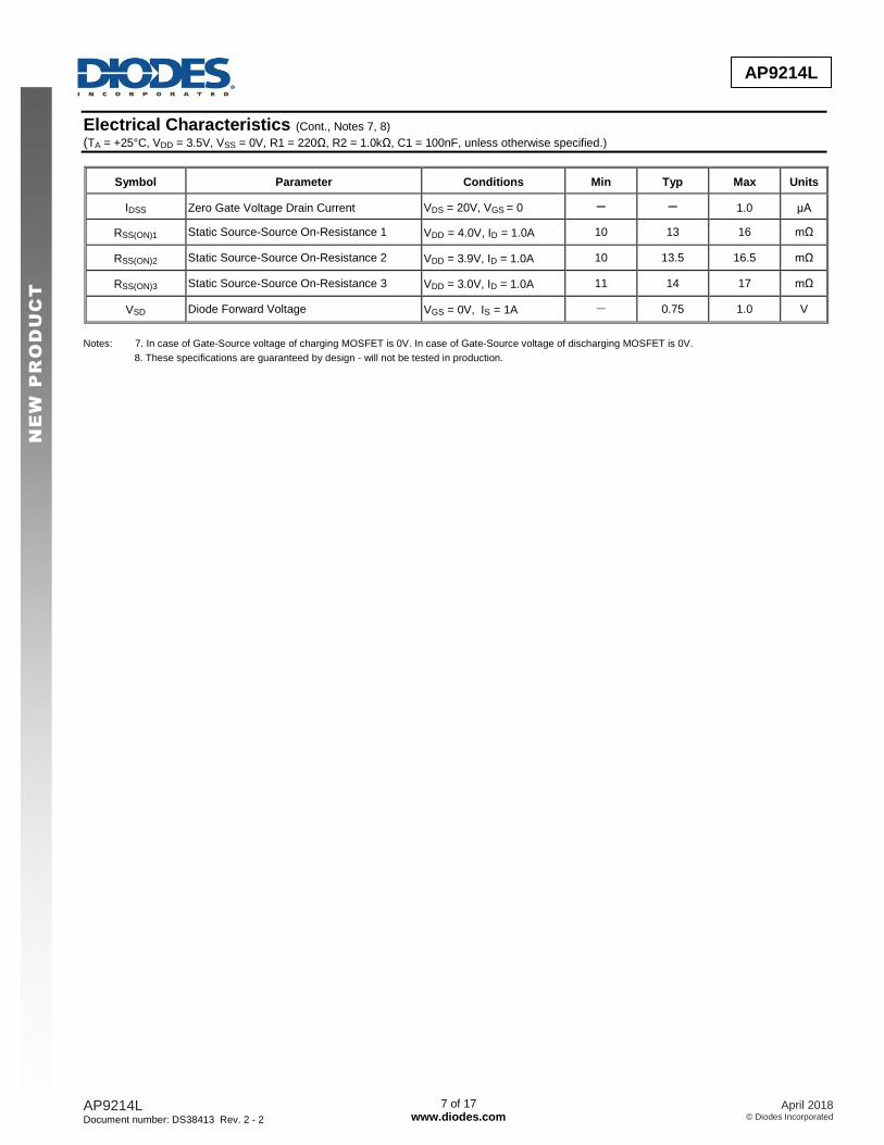
Electrical Characteristics (Cont., Notes 7, 8) (TA = +25°C, VDD = 3.5V, VSS = 0V, R1 = 220Ω, R2 = 1.0kΩ, C1 = 100nF, unless otherwise specified.)
Symbol Parameter Conditions Min Typ Max Units
IDSS Zero Gate Voltage Drain Current VDS = 20V, VGS = 0 - - 1.0 μA
RSS(ON)1 Static Source-Source On-Resistance 1 VDD = 4.0V, ID = 1.0A 10 13 16 mΩ
RSS(ON)2 Static Source-Source On-Resistance 2 VDD = 3.9V, ID = 1.0A 10 13.5 16.5 mΩ
RSS(ON)3 Static Source-Source On-Resistance 3 VDD = 3.0V, ID = 1.0A 11 14 17 mΩ
VSD Diode Forward Voltage VGS = 0V, IS = 1A - 0.75 1.0 V
Notes: 7. In case of Gate-Source voltage of charging MOSFET is 0V. In case of Gate-Source voltage of discharging MOSFET is 0V.
8. These specifications are guaranteed by design - will not be tested in production.
AP9214L Document number: DS38413 Rev. 2 - 2
8 of 17 www.diodes.com
April 2018 © Diodes Incorporated
AP9214L
NE
W P
RO
DU
CT
Application Information
Operation Mode
1. Normal Status
The AP9214L monitors the battery voltage between the VDD pin and VSS pin as well as the voltage difference between the VM pin and VSS pin
to control battery charging and discharging. When the battery voltage is between overdischarge detection voltage (VDL) and overcharge detection
voltage (VCU) as well as the VM pin voltage is between the charge overcurrent detection voltage (VCOC) and discharge overcurrent detection
voltage (VDOC), the AP9214L will turn on discharging and charging MOSFET. In these conditions, the battery can charge and discharge freely.
Also, RVMD does not connect to VDD pin and RVMS does not connect to VSS pin in this status.
2. Overcharge Status
If the battery voltage is more than VCU during charging status for the overcharge detection delay time (tCU) or longer, the AP9214L turns off the
charging MOSFET to stop charging. RVMD and RVMS are not connected in overcharge status.
When VM pin voltage is lower than VDOC and battery voltage falls below VCL, the AP9214L will release from overcharge status.
When VM pin voltage is equal or more than VDOC and battery voltage falls below VCU, the AP9214L will release from overcharge status.
3. Overdischarge Status
If the battery voltage is less than VDL during discharging status for the overdischarge detection delay time (tDL) or longer, the AP9214L turns off the
discharging MOSFET to stop discharging. In overdischarge status, RVMD is connected to VDD and VM pin voltage is pulled up to VDD by RVMD,
but RVMS is not connected.
For power-down mode version, the AP9214L recovers normal status from overdischarge status only by charging the battery through the charger.
When VM pin voltage to VSS pin voltage is less than typical -0.7V and the battery voltage rises over VDL, the AP9214L will release from
overdischarge status. If VM pin voltage to VSS pin voltage is higher than typical -0.7V, the AP9214L will release from overdischarge status until
the battery voltage rises over VDU.
For auto-wake-up version AP9214LA, the device recovers to normal status from overdischarge status if either of these two conditions are satisfied:
If charger is connected: the AP9214LA overdischarge status is released in the same way as described above in AP9214L overdischarge Status section.
If no charger is connected: 1) The battery voltage reaches the overdischarge release voltage (VDU) or higher;
2) Maintains continuous time more than overdischarge release delay time tDLR.
4. Discharge Overcurrent and Short Current Status
When battery is in discharge overcurrent status, if the voltage of the VM pin to VSS pin is equal or more than VDOC to VSHORT and detection lasts
for the discharge overcurrent detection delay time (tDOC) or longer, the AP9214L turns off the discharging MOSFET to stop discharging.
When the battery is in short current status, if the voltage of the VM pin to VSS pin is equal to or more than VSHORT, and the detection lasts for the
short current detection delay time or longer, the AP9214L turns off the discharge MOSFET to stop discharging.
In discharge overcurrent or short current status, RVMS is connected to VSS but RVMD is not connected. The voltage of VM pin is almost equal to
VDD as long as the load is connected. When the load is disconnected, the voltage of VM pin will become almost equal to VSS (due to RVMS being
connected) and then the AP9214L will release from discharge overcurrent or short current status.
5. Charge Overcurrent Status
When the battery is in charge overcurrent status, if the voltage of the VM pin to VSS pin is equal to or less than VCOC and the detection continues
for the charge overcurrent detection delay time (tCOC) or longer, the AP9214L turns off the charging MOSFET to stop charging.
6. 0V Battery Charging Function (Optional)
This function is available as an option and can be factory set internally. The AP9214L has this function built in.
0V charging function permits charger to recharge the battery whose voltage is 0V due to self-discharge. If 0V charging function is not present, the
device will prevent charger to recharge the battery whose voltage is 0V due to self-discharge. (If a device without 0V charging function is needed,
please contact Diodes sales team.)
AP9214L Document number: DS38413 Rev. 2 - 2
9 of 17 www.diodes.com
April 2018 © Diodes Incorporated
AP9214L
NE
W P
RO
DU
CT
Application Information (Cont.)
7. Overvoltage Charger Detection Circuit
This function is used to monitor the charger voltage between the VDD pin and VM pin, and when this voltage exceeds overvoltage charger
detection voltage (8.0V Typ.), the AP9214L will turn off charging MOSFET, when this voltage drops below overvoltage charger release voltage
(7.3V Typ.), it then turns on charging MOSFET. There is no delay time setting for detection and release.
8. Power-Down Mode or Auto-Wake-Up Function (Optional)
In device with power-down function, during power-down mode, device enters the overdischarge status. The IC enters sleep mode and the current
consumption becomes very low, typically 0.1μA. To release from power-down status to the normal status, charger connection is required.
In device with auto-wakeup mode, the IC remains active in the overdischarge state. The IC is released into the normal state by the operation that
increases the battery voltage more than overdischarge release voltage.
AP9214L Document number: DS38413 Rev. 2 - 2
10 of 17 www.diodes.com
April 2018 © Diodes Incorporated
AP9214L
NE
W P
RO
DU
CT
Application Information (Timing Chart) 1. Overcharge and Overdischarge Detection
VCU
VCL
VDL
VDU
VDD
VSS
VSS
VDD
VVM
VDD
VDOC
VSS
VP-
VCOC
VDD
DO
CO
VM
2 1
Red line is for
no shutdown
mode version
1: tDL
2: tCU
3: tCUR
4: tDLR
2 1S1 S1 S2S2
3 4 3 3
S1: Charger connection
S2: Load connection
P1: RVMD pull-up connection
P1 P1
AP9214L Document number: DS38413 Rev. 2 - 2
11 of 17 www.diodes.com
April 2018 © Diodes Incorporated
AP9214L
NE
W P
RO
DU
CT
Application Information (Timing Chart) (Cont.)
2. Discharge Overcurrent Detection
VCU
VCL
VDL
VDU
ON
VSS
OFF
ON
OFF
VDD
VSHORT
VSS
VDOC
VDD
DO
CO
VM
1 2
S1 S2
1: tDOC
2: tSHORT
3: tDOCR
S1: Connect over current load
S2: Connect short current load
P1: RVMS pull-down connection
3 3
P1P1
1
AP9214L Document number: DS38413 Rev. 2 - 2
12 of 17 www.diodes.com
April 2018 © Diodes Incorporated
AP9214L
NE
W P
RO
DU
CT
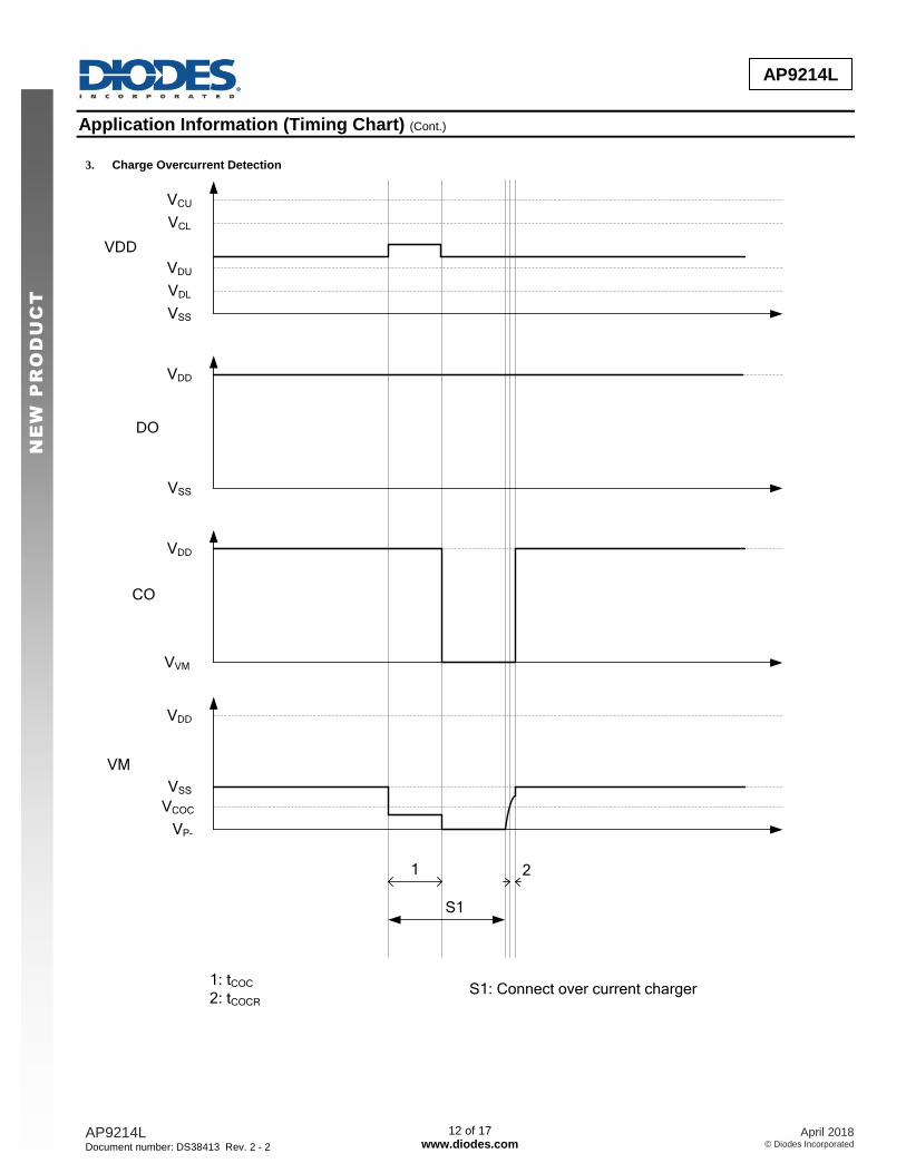
Application Information (Timing Chart) (Cont.)
3. Charge Overcurrent Detection
VCU
VCL
VDL
VDU
VDD
VSS
VSS
VDD
VVM
VDD
VSS
VP-
VCOC
VDD
DO
CO
VM
1
S1
1: tCOC
2: tCOCRS1: Connect over current charger
2
AP9214L Document number: DS38413 Rev. 2 - 2
13 of 17 www.diodes.com
April 2018 © Diodes Incorporated
AP9214L
NE
W P
RO
DU
CT
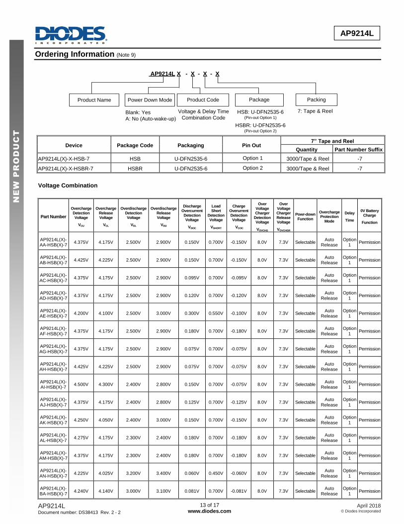
Ordering Information (Note 9)
AP9214L X - X - X - X
Product Code
Voltage & Delay Time
Combination CodeHSB: U-DFN2535-6
(Pin-out Option 1)
HSBR: U-DFN2535-6(Pin-out Option 2)
Packing
7: Tape & Reel
Power Down Mode
Blank: Yes
A: No (Auto-wake-up)
PackageProduct Name
Device Package Code Packaging Pin Out 7” Tape and Reel
Quantity Part Number Suffix
AP9214L(X)-X-HSB-7 HSB U-DFN2535-6 Option 1 3000/Tape & Reel -7
AP9214L(X)-X-HSBR-7 HSBR U-DFN2535-6 Option 2 3000/Tape & Reel -7
Voltage Combination
Part Number
Overcharge Detection Voltage
VCU
Overcharge Release Voltage
VCL
Overdischarge Detection Voltage
VDL
Overdischarge Release Voltage
VDU
Discharge Overcurrent
Detection Voltage
VDOC
Load Short
Detection Voltage
VSHORT
Charge Overurrent Detection Voltage
VCOC
Over Voltage Charger
Detection Voltage
VOVCHG
Over Voltage Charger Release Voltage
VOVCHGR
Powr-down Function
Overcharge Protection
Mode
Delay
Time
0V Battery Charge
Function
AP9214L(X)-AA-HSB(X)-7
4.375V 4.175V 2.500V 2.900V 0.150V 0.700V -0.150V 8.0V 7.3V Selectable Auto
Release Option
1 Permission
AP9214L(X)-AB-HSB(X)-7
4.425V 4.225V 2.500V 2.900V 0.150V 0.700V -0.150V 8.0V 7.3V Selectable Auto
Release Option
1 Permission
AP9214L(X)-AC-HSB(X)-7
4.375V 4.175V 2.500V 2.900V 0.095V 0.700V -0.095V 8.0V 7.3V Selectable Auto
Release Option
1 Permission
AP9214L(X)-AD-HSB(X)-7
4.375V 4.175V 2.500V 2.900V 0.120V 0.700V -0.120V 8.0V 7.3V Selectable Auto
Release Option
1 Permission
AP9214L(X)-AE-HSB(X)-7
4.200V 4.100V 2.500V 3.000V 0.300V 0.550V -0.100V 8.0V 7.3V Selectable Auto
Release Option
1 Permission
AP9214L(X)-AF-HSB(X)-7
4.375V 4.175V 2.500V 2.900V 0.180V 0.700V -0.180V 8.0V 7.3V Selectable Auto
Release Option
1 Permission
AP9214L(X)-AG-HSB(X)-7
4.375V 4.175V 2.500V 2.900V 0.075V 0.700V -0.075V 8.0V 7.3V Selectable Auto
Release Option
1 Permission
AP9214L(X)-AH-HSB(X)-7
4.425V 4.225V 2.500V 2.900V 0.075V 0.700V -0.075V 8.0V 7.3V Selectable Auto
Release Option
1 Permission
AP9214L(X)-AI-HSB(X)-7
4.500V 4.300V 2.400V 2.800V 0.150V 0.700V -0.075V 8.0V 7.3V Selectable Auto
Release Option
1 Permission
AP9214L(X)-AJ-HSB(X)-7
4.375V 4.175V 2.400V 2.800V 0.125V 0.700V -0.125V 8.0V 7.3V Selectable Auto
Release Option
1 Permission
AP9214L(X)-AK-HSB(X)-7
4.250V 4.050V 2.400V 3.000V 0.150V 0.700V -0.150V 8.0V 7.3V Selectable Auto
Release Option
1 Permission
AP9214L(X)-AL-HSB(X)-7
4.275V 4.175V 2.300V 2.400V 0.180V 0.700V -0.180V 8.0V 7.3V Selectable Auto
Release Option
1 Permission
AP9214L(X)-AM-HSB(X)-7
4.375V 4.175V 2.300V 2.400V 0.180V 0.700V -0.180V 8.0V 7.3V Selectable Auto
Release Option
1 Permission
AP9214L(X)-AN-HSB(X)-7
4.225V 4.025V 3.200V 3.400V 0.060V 0.450V -0.060V 8.0V 7.3V Selectable Auto
Release Option
1 Permission
AP9214L(X)-BA-HSB(X)-7
4.240V 4.140V 3.000V 3.100V 0.081V 0.700V -0.081V 8.0V 7.3V Selectable Auto
Release Option
1 Permission
AP9214L Document number: DS38413 Rev. 2 - 2
14 of 17 www.diodes.com
April 2018 © Diodes Incorporated
AP9214L
NE
W P
RO
DU
CT
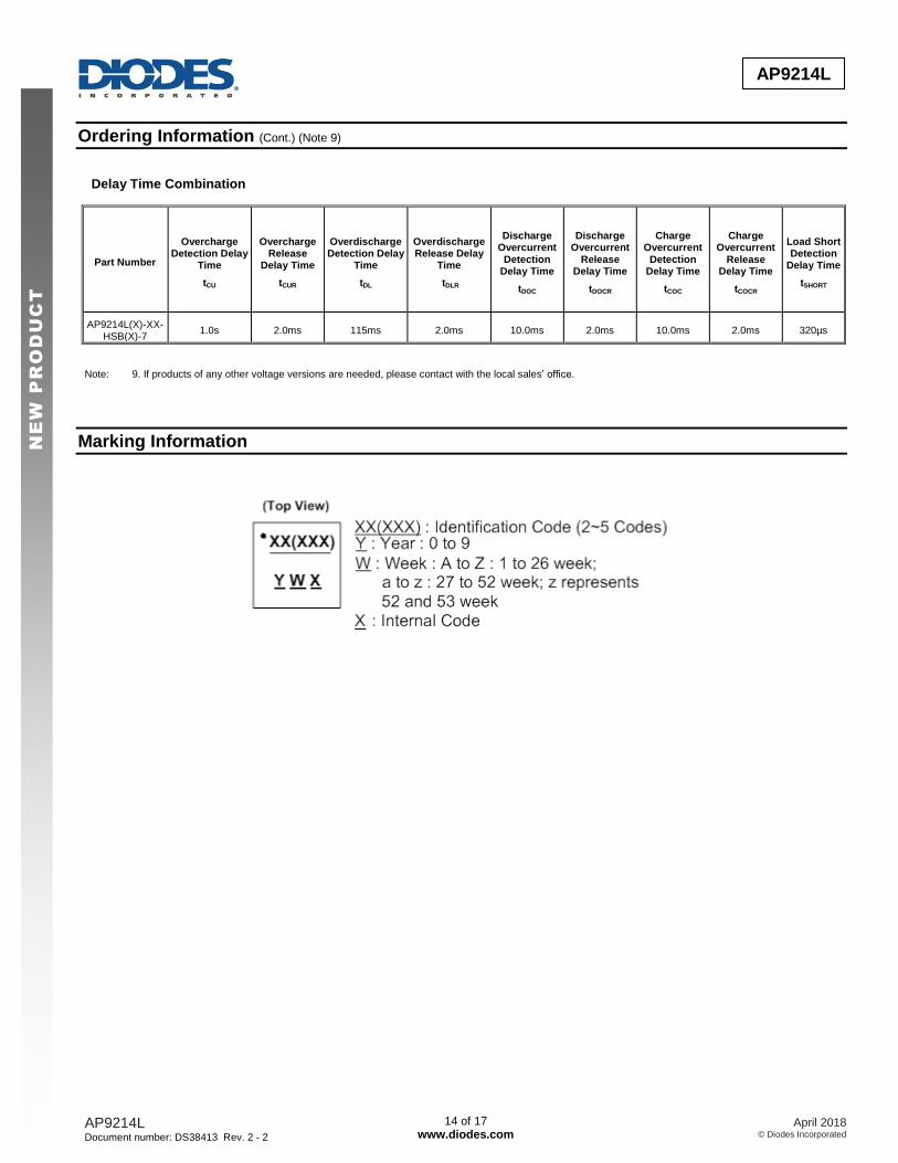
Ordering Information (Cont.) (Note 9)
Delay Time Combination
Part Number
Overcharge Detection Delay
Time
tCU
Overcharge Release
Delay Time
tCUR
Overdischarge Detection Delay
Time
tDL
Overdischarge Release Delay
Time
tDLR
Discharge Overcurrent
Detection Delay Time
tDOC
Discharge Overcurrent
Release Delay Time
tDOCR
Charge Overcurrent
Detection Delay Time
tCOC
Charge Overcurrent
Release Delay Time
tCOCR
Load Short Detection
Delay Time
tSHORT
AP9214L(X)-XX-HSB(X)-7
1.0s 2.0ms 115ms 2.0ms 10.0ms 2.0ms 10.0ms 2.0ms 320µs
Note: 9. If products of any other voltage versions are needed, please contact with the local sales’ office.
Marking Information
AP9214L Document number: DS38413 Rev. 2 - 2
15 of 17 www.diodes.com
April 2018 © Diodes Incorporated
AP9214L
NE
W P
RO
DU
CT
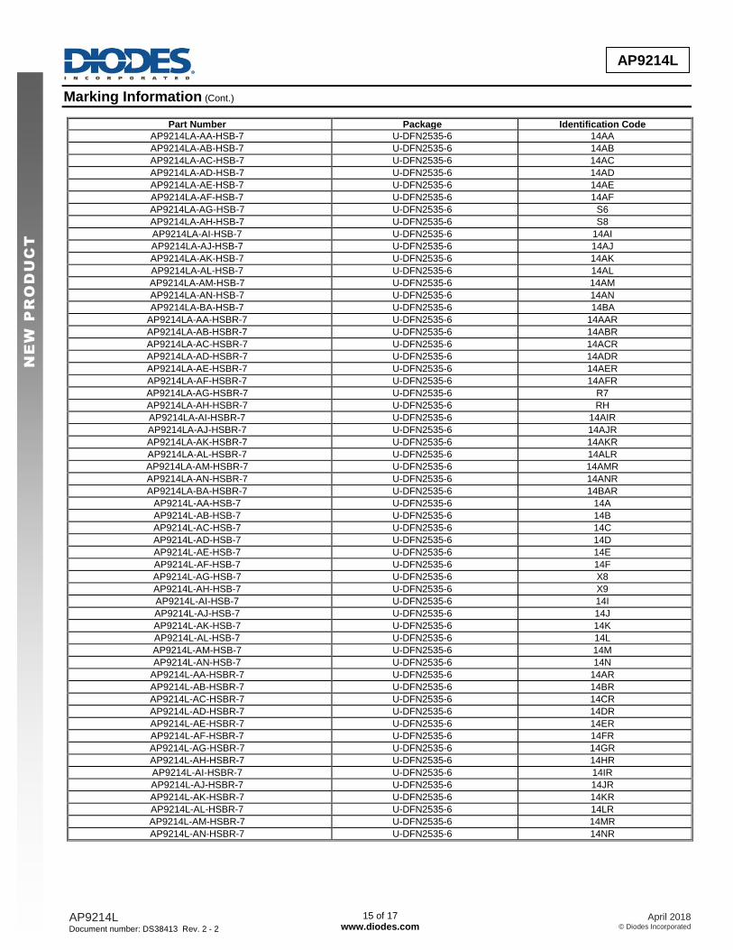
Marking Information (Cont.)
Part Number Package Identification Code
AP9214LA-AA-HSB-7 U-DFN2535-6 14AA
AP9214LA-AB-HSB-7 U-DFN2535-6 14AB
AP9214LA-AC-HSB-7 U-DFN2535-6 14AC
AP9214LA-AD-HSB-7 U-DFN2535-6 14AD
AP9214LA-AE-HSB-7 U-DFN2535-6 14AE
AP9214LA-AF-HSB-7 U-DFN2535-6 14AF
AP9214LA-AG-HSB-7 U-DFN2535-6 S6
AP9214LA-AH-HSB-7 U-DFN2535-6 S8
AP9214LA-AI-HSB-7 U-DFN2535-6 14AI
AP9214LA-AJ-HSB-7 U-DFN2535-6 14AJ
AP9214LA-AK-HSB-7 U-DFN2535-6 14AK
AP9214LA-AL-HSB-7 U-DFN2535-6 14AL
AP9214LA-AM-HSB-7 U-DFN2535-6 14AM
AP9214LA-AN-HSB-7 U-DFN2535-6 14AN
AP9214LA-BA-HSB-7 U-DFN2535-6 14BA
AP9214LA-AA-HSBR-7 U-DFN2535-6 14AAR
AP9214LA-AB-HSBR-7 U-DFN2535-6 14ABR
AP9214LA-AC-HSBR-7 U-DFN2535-6 14ACR
AP9214LA-AD-HSBR-7 U-DFN2535-6 14ADR
AP9214LA-AE-HSBR-7 U-DFN2535-6 14AER
AP9214LA-AF-HSBR-7 U-DFN2535-6 14AFR
AP9214LA-AG-HSBR-7 U-DFN2535-6 R7
AP9214LA-AH-HSBR-7 U-DFN2535-6 RH
AP9214LA-AI-HSBR-7 U-DFN2535-6 14AIR
AP9214LA-AJ-HSBR-7 U-DFN2535-6 14AJR
AP9214LA-AK-HSBR-7 U-DFN2535-6 14AKR
AP9214LA-AL-HSBR-7 U-DFN2535-6 14ALR
AP9214LA-AM-HSBR-7 U-DFN2535-6 14AMR
AP9214LA-AN-HSBR-7 U-DFN2535-6 14ANR
AP9214LA-BA-HSBR-7 U-DFN2535-6 14BAR
AP9214L-AA-HSB-7 U-DFN2535-6 14A
AP9214L-AB-HSB-7 U-DFN2535-6 14B
AP9214L-AC-HSB-7 U-DFN2535-6 14C
AP9214L-AD-HSB-7 U-DFN2535-6 14D
AP9214L-AE-HSB-7 U-DFN2535-6 14E
AP9214L-AF-HSB-7 U-DFN2535-6 14F
AP9214L-AG-HSB-7 U-DFN2535-6 X8
AP9214L-AH-HSB-7 U-DFN2535-6 X9
AP9214L-AI-HSB-7 U-DFN2535-6 14I
AP9214L-AJ-HSB-7 U-DFN2535-6 14J
AP9214L-AK-HSB-7 U-DFN2535-6 14K
AP9214L-AL-HSB-7 U-DFN2535-6 14L
AP9214L-AM-HSB-7 U-DFN2535-6 14M
AP9214L-AN-HSB-7 U-DFN2535-6 14N
AP9214L-AA-HSBR-7 U-DFN2535-6 14AR
AP9214L-AB-HSBR-7 U-DFN2535-6 14BR
AP9214L-AC-HSBR-7 U-DFN2535-6 14CR
AP9214L-AD-HSBR-7 U-DFN2535-6 14DR
AP9214L-AE-HSBR-7 U-DFN2535-6 14ER
AP9214L-AF-HSBR-7 U-DFN2535-6 14FR
AP9214L-AG-HSBR-7 U-DFN2535-6 14GR
AP9214L-AH-HSBR-7 U-DFN2535-6 14HR
AP9214L-AI-HSBR-7 U-DFN2535-6 14IR
AP9214L-AJ-HSBR-7 U-DFN2535-6 14JR
AP9214L-AK-HSBR-7 U-DFN2535-6 14KR
AP9214L-AL-HSBR-7 U-DFN2535-6 14LR
AP9214L-AM-HSBR-7 U-DFN2535-6 14MR
AP9214L-AN-HSBR-7 U-DFN2535-6 14NR
AP9214L Document number: DS38413 Rev. 2 - 2
16 of 17 www.diodes.com
April 2018 © Diodes Incorporated
AP9214L
NE
W P
RO
DU
CT
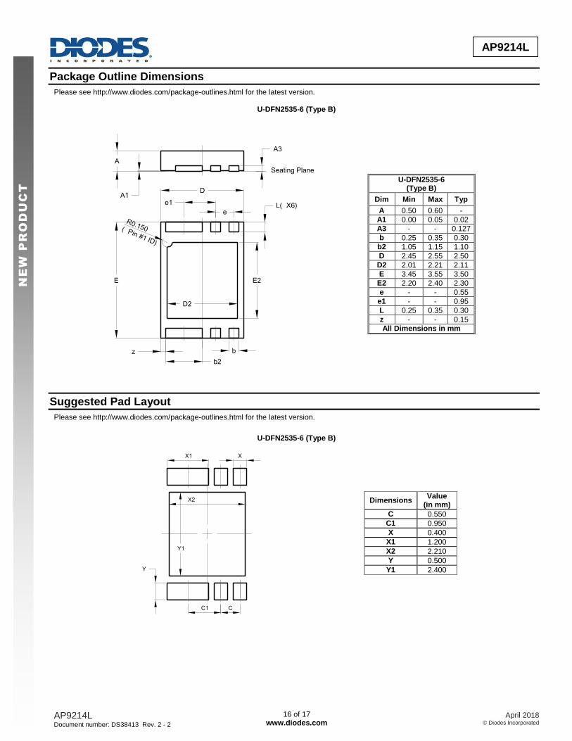
Package Outline Dimensions
Please see http://www.diodes.com/package-outlines.html for the latest version.
U-DFN2535-6 (Type B)
b2
e1
R0.150
z
A
A1
A3
Seating Plane
D
E
e
b
(Pin #1 ID)
D2
E2
L(X6)
U-DFN2535-6 (Type B)
Dim Min Max Typ
A 0.50 0.60 -
A1 0.00 0.05 0.02
A3 - - 0.127
b 0.25 0.35 0.30
b2 1.05 1.15 1.10
D 2.45 2.55 2.50
D2 2.01 2.21 2.11
E 3.45 3.55 3.50
E2 2.20 2.40 2.30
e - - 0.55
e1 - - 0.95
L 0.25 0.35 0.30
z - - 0.15
All Dimensions in mm
Suggested Pad Layout
Please see http://www.diodes.com/package-outlines.html for the latest version.
U-DFN2535-6 (Type B)
XX1
CC1
Y1
X2
Y
Dimensions Value
(in mm)
C 0.550
C1 0.950
X 0.400
X1 1.200
X2 2.210
Y 0.500
Y1 2.400
AP9214L Document number: DS38413 Rev. 2 - 2
17 of 17 www.diodes.com
April 2018 © Diodes Incorporated
AP9214L
NE
W P
RO
DU
CT
IMPORTANT NOTICE DIODES INCORPORATED MAKES NO WARRANTY OF ANY KIND, EXPRESS OR IMPLIED, WITH REGARDS TO THIS DOCUMENT, INCLUDING, BUT NOT LIMITED TO, THE IMPLIED WARRANTIES OF MERCHANTABILITY AND FITNESS FOR A PARTICULAR PURPOSE (AND THEIR EQUIVALENTS UNDER THE LAWS OF ANY JURISDICTION). Diodes Incorporated and its subsidiaries reserve the right to make modifications, enhancements, improvements, corrections or other changes without further notice to this document and any product described herein. Diodes Incorporated does not assume any liability arising out of the application or use of this document or any product described herein; neither does Diodes Incorporated convey any license under its patent or trademark rights, nor the rights of others. Any Customer or user of this document or products described herein in such applications shall assume all risks of such use and will agree to hold Diodes Incorporated and all the companies whose products are represented on Diodes Incorporated website, harmless against all damages. Diodes Incorporated does not warrant or accept any liability whatsoever in respect of any products purchased through unauthorized sales channel. Should Customers purchase or use Diodes Incorporated products for any unintended or unauthorized application, Customers shall indemnify and hold Diodes Incorporated and its representatives harmless against all claims, damages, expenses, and attorney fees arising out of, directly or indirectly, any claim of personal injury or death associated with such unintended or unauthorized application. Products described herein may be covered by one or more United States, international or foreign patents pending. Product names and markings noted herein may also be covered by one or more United States, international or foreign trademarks. This document is written in English but may be translated into multiple languages for reference. Only the English version of this document is the final and determinative format released by Diodes Incorporated.
LIFE SUPPORT Diodes Incorporated products are specifically not authorized for use as critical components in life support devices or systems without the express written approval of the Chief Executive Officer of Diodes Incorporated. As used herein: A. Life support devices or systems are devices or systems which: 1. are intended to implant into the body, or
2. support or sustain life and whose failure to perform when properly used in accordance with instructions for use provided in the labeling can be reasonably expected to result in significant injury to the user.
B. A critical component is any component in a life support device or system whose failure to perform can be reasonably expected to cause the failure of the life support device or to affect its safety or effectiveness. Customers represent that they have all necessary expertise in the safety and regulatory ramifications of their life support devices or systems, and acknowledge and agree that they are solely responsible for all legal, regulatory and safety-related requirements concerning their products and any use of Diodes Incorporated products in such safety-critical, life support devices or systems, notwithstanding any devices- or systems-related information or support that may be provided by Diodes Incorporated. Further, Customers must fully indemnify Diodes Incorporated and its representatives against any damages arising out of the use of Diodes Incorporated products in such safety-critical, life support devices or systems. Copyright © 2018, Diodes Incorporated www.diodes.com