Embed Size (px)
Citation preview
Thin Solid Films 459(2004) 7–12
0040-6090/04/$ - see front matter� 2003 Elsevier B.V. All rights reserved.doi:10.1016/j.tsf.2003.12.140
Deposition of epitaxial silicon carbide films using high vacuum MOCVDmethod for MEMS applications
D.-C. Lim , H.-G. Jee , J.W. Kim , J.-S. Moon , S.-B. Lee , S.S. Choi , J.-H. Boo *a a a a a b a,
Department of Chemistry, Sungkyunkwan University, 300 Chunchun-Dong, Jangan-Gu, Suwon 440-746, South Koreaa
Department of Nanoscience, Sunmoon University, Ahsan 336-840, South Koreab
Available Online April 2 2004
Abstract
Silicon carbide(SiC) thin film have been prepared on both Si(100) and SiO patterned Si(100) substrates by the high vacuum2
metal-organic chemical vapor deposition(MOCVD) method using a single source precursor at various growth temperatures inthe range of 700–10008C. Diethylmethylsilane(DEMS) was used as precursor without carrier gas. The effects of substratetemperature as well as deposition time on the crystal growth and hardness were mainly investigated in this study. The optimumtemperature for the formation of the epitaxial SiC thin films were found to 9008C on the basis of XRD results. However, theXPS result shows that the SiC film grown at 9008C have carbon rich(Si:Cs1:1.2 composition) surface due to surface reactionof the precursor itself. From the SEM images, substrate temperature has influence on the grain size and crystallinity of the SiCfilms. Especially, the major crystal form of these deposited films was rectangular in shape on the substrates at 9008C. We alsoobtain a high hardness SiC thin film with 32 GPa.� 2003 Elsevier B.V. All rights reserved.
Keywords: High vacuum metal-organic chemical vapor deposition(MOCVD); Epitxial SiC thin film; Diethylmethylsilane(DEMS); Selectivedeposition of SiC
1. Introduction
The advances in silicon process technology over thelast 3 decades has led to the development of microcom-ponents known as microelectromechanical system orMEMS (Micro-Electro-Mechanical-Systems). Althoughsilicon based MEMS devices find such wide uses today,they lack high temperature capabilities with respect toboth mechanical and electrical properties. Recently,researchers have been pursuing SiC as material for high-temperature microsensor and microactuator applicationsw1–4x.Silicon carbide become generally known as attractive
material for demanding mechanical and high-tempera-ture application, as well as for use in abrasive, erosive,and corrosive media. Also, SiC is semiconductor ofgreat interest in high-power, high-temperature, and high-radiation applicationsw5–7x. Thus, the superior mechan-ical, chemical, and electrical capabilities make SiC anexceptionally attractive material in MEMS applications.
*Corresponding author. Tel.:q82-31-290-7072; fax:q82-31-290-7075.
E-mail address: [email protected](J.-H. Boo).
Conventional silicon carbide chemical-vapor-deposi-tion (CVD) processes generally utilized multiple pre-cursors such as silane and hydrocarbons and requiredelevated substrate temperatures in excess of 10008C.High growth temperature sometimes results in hightensile stress and lattice defects in the SiC films becauseof the differences in lattice constants and thermal expan-sion coefficients between silicon carbide and siliconw8x.Therefore, low-temperature alternatives to the conven-tional SiC CVD methods must be considered. To dothis, a simple CVD method utilizing a single precursoris highly desirable for growing high-quality SiC filmsat temperature below 10008C to enable SiC post-processing such etchingw9x. In this study, therefore, wehave deposited epitaxial cubic-SiC thin films on Si(001) and patterned SiO Si(100) substrates at temper-2
atures of 700–10008C utilizing diethylmethylsilane(DEMS) as a single precursor for MEMS applications.
2. Experimental
Crystalline SiC thin films were fabricated in a parallellow-pressure MOCVD reactor. Inside the reactor, the
8 D.-C. Lim et al. / Thin Solid Films 459 (2004) 7–12
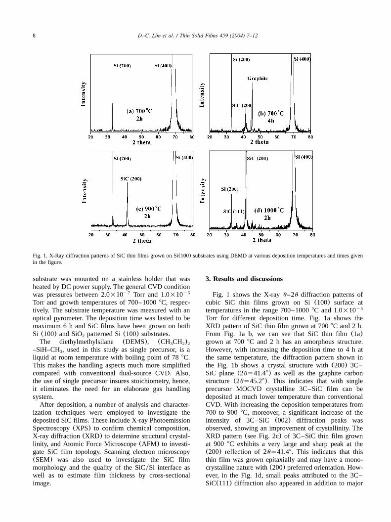
Fig. 1. X-Ray diffraction patterns of SiC thin films grown on Si(100) substrates using DEMD at various deposition temperatures and times givenin the figure.
substrate was mounted on a stainless holder that washeated by DC power supply. The general CVD conditionwas pressures between 2.0=10 Torr and 1.0=10y7 y5
Torr and growth temperatures of 700–10008C, respec-tively. The substrate temperature was measured with anoptical pyrometer. The deposition time was lasted to bemaximum 6 h and SiC films have been grown on bothSi (100) and SiO patterned Si(100) substrates.2
The diethylmethylsilane (DEMS), (CH CH )3 2 2
–SiH–CH , used in this study as single precursor, is a3
liquid at room temperature with boiling point of 788C.This makes the handling aspects much more simplifiedcompared with conventional dual-source CVD. Also,the use of single precursor insures stoichiometry, hence,it eliminates the need for an elaborate gas handlingsystem.After deposition, a number of analysis and character-
ization techniques were employed to investigate thedeposited SiC films. These include X-ray PhotoemissionSpectroscopy(XPS) to confirm chemical composition,X-ray diffraction (XRD) to determine structural crystal-linity, and Atomic Force Microscope(AFM) to investi-gate SiC film topology. Scanning electron microscopy(SEM) was also used to investigate the SiC filmmorphology and the quality of the SiCySi interface aswell as to estimate film thickness by cross-sectionalimage.
3. Results and discussions
Fig. 1 shows the X-rayu–2u diffraction patterns ofcubic SiC thin films grown on Si(100) surface attemperatures in the range 700–10008C and 1.0=10y5
Torr for different deposition time. Fig. 1a shows theXRD pattern of SiC thin film grown at 7008C and 2 h.From Fig. 1a b, we can see that SiC thin film(1a)grown at 7008C and 2 h has an amorphous structure.However, with increasing the deposition time to 4 h atthe same temperature, the diffraction pattern shown inthe Fig. 1b shows a crystal structure with(200) 3C–SiC plane(2us41.48) as well as the graphite carbonstructure (2us45.28). This indicates that with singleprecursor MOCVD crystalline 3C–SiC film can bedeposited at much lower temperature than conventionalCVD. With increasing the deposition temperatures from700 to 9008C, moreover, a significant increase of theintensity of 3C–SiC (002) diffraction peaks wasobserved, showing an improvement of crystallinity. TheXRD pattern(see Fig. 2c) of 3C–SiC thin film grownat 900 8C exhibits a very large and sharp peak at the(200) reflection of 2us41.48. This indicates that thisthin film was grown epitaxially and may have a mono-crystalline nature with(200) preferred orientation. How-ever, in the Fig. 1d, small peaks attributed to the 3C–SiC(111) diffraction also appeared in addition to major

9D.-C. Lim et al. / Thin Solid Films 459 (2004) 7–12
Fig. 2. SEM images of SiC thin films grown on Si(100) substrates using DEMS at various deposition temperatures.
peaks of 3C–SiC(200) diffraction, indicating thatpolycrystalline 3C–SiC thin film was obtained at dep-osition temperatures of 10008C. From our XRD data,with increasing the deposition temperature from 700 to900 8C, high quality 3C–SiC layer was obtained underthe same deposition conditions. The XRD results alsoshow that the deposition time as well as depositiontemperature could be one of the important factors forinfluencing the film crystallinity.Fig. 2 shows surface morphology changes of the 3C–
SiC films grown at various temperatures(700–10008C)for 2 h under the same deposition pressure of 1.0Torr=10 Torr, respectively. We can see that the filmy5
grown at 7008C has a smooth surface and nano sizeSiC crystals as shown in the Fig. 2a. With increasingthe deposition temperature, 3C–SiC film with relativelylarge crystals were deposited. The surface morphologiesof the films grown at 900 and 10008C show muchlarger crystal size than those of the films grown at 700and 8008C. The SEM image of SiC film grown at 8008C shown in the Fig. 2b exhibits a crystal shape of SiCcrystals with sub-micron size. Above 8008C, the crystalsize and crystallinity of the 3C–SiC films are apparentlylimited to the substrate temperature. Especially, from theFig. 2c, we can see that the major crystal form of adeposited film grown on the substrate at 9008C isrectangular in shape. We also confirm the crystal formof the SiC film deposited at 9008C from a AFM result(see Fig. 4a,c). However, a polycrystalline shape with
relatively larger crystal size can be seen in Fig. 2d,when the growth temperature was at 10008C. This isin good agreement with the XRD result shown in theFig. 1d.Film stoichiometry of the 3C–SiC film with opti-
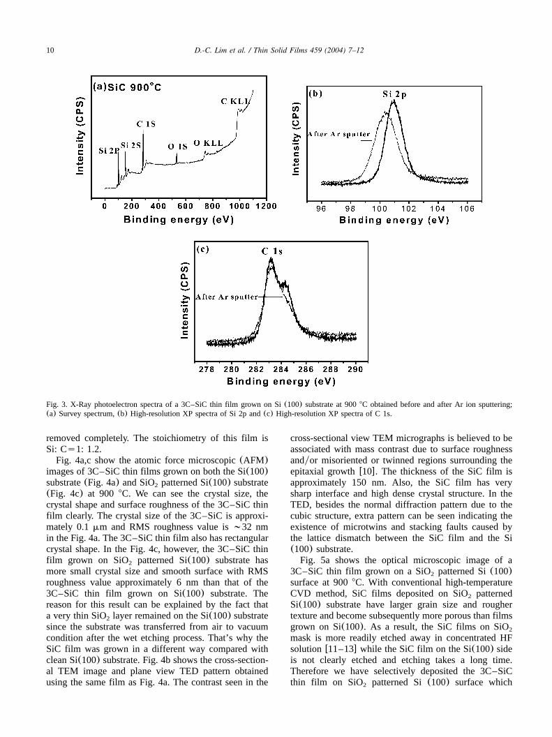
mized expitaxial crystal structure was determined util-izing the XPS analysis. The survey spectrum of Fig. 3aclearly shows the photoelectron peaks of Si 2s, Si 2p,C1s and C(KLL ) Auger signals indicating formationof silicon carbide film. Oxygen(O 1s) can be attributedto surface contamination by moisture during sampletransfer in the air condition. Also, we could see that thecarbon content decreased after the Ar ion sputtering asshown in the Fig. 3c. As the sputtering depth is lessthan 3 nm, the carbon is the adsorbed species on theSiC surface. The reason for arising the carbon contenton the surface is mainly due to the air contaminationafter deposition. In Fig. 3b, the Si 1s high-resolutionspectra obtained before and after Ar ion sputtering arealso shown. To compare the change of Si 1s bindingenergies for the SiC film before and after Ar ionsputtering, the Si 1s peak at 100.9 eV obtained withoutAr ion sputtering is shifted to lower binging energy at100.3 eV after Ar ion sputtering. The reason for thisbinding energy shift is due to increasing of carbidicafter removing of graphite carbon and surface SiOx
species by Ar ion sputtering. However, we also seeweak carbon shoulder peak in Fig. 5c but if we didmore Ar ion sputtering the graphite carbon can be
10 D.-C. Lim et al. / Thin Solid Films 459 (2004) 7–12
Fig. 3. X-Ray photoelectron spectra of a 3C–SiC thin film grown on Si(100) substrate at 9008C obtained before and after Ar ion sputtering;(a) Survey spectrum,(b) High-resolution XP spectra of Si 2p and(c) High-resolution XP spectra of C 1s.
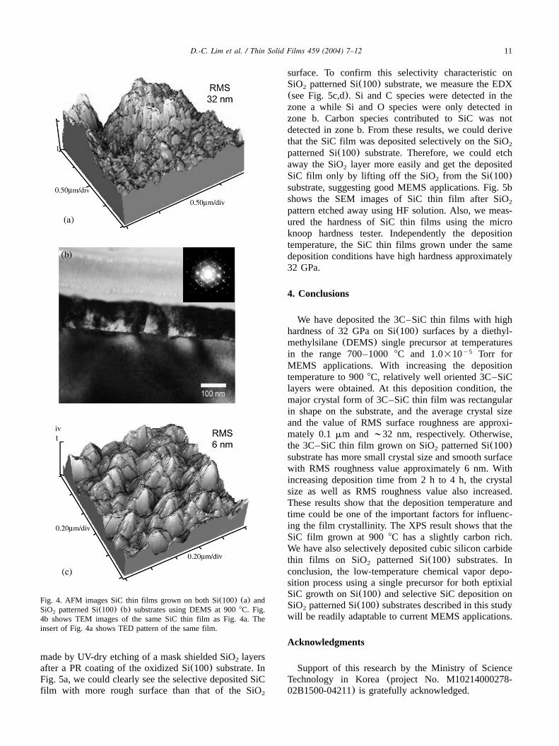
removed completely. The stoichiometry of this film isSi: Cs1: 1.2.Fig. 4a,c show the atomic force microscopic(AFM)
images of 3C–SiC thin films grown on both the Si(100)substrate(Fig. 4a) and SiO patterned Si(100) substrate2
(Fig. 4c) at 900 8C. We can see the crystal size, thecrystal shape and surface roughness of the 3C–SiC thinfilm clearly. The crystal size of the 3C–SiC is approxi-mately 0.1mm and RMS roughness value is;32 nmin the Fig. 4a. The 3C–SiC thin film also has rectangularcrystal shape. In the Fig. 4c, however, the 3C–SiC thinfilm grown on SiO patterned Si(100) substrate has2
more small crystal size and smooth surface with RMSroughness value approximately 6 nm than that of the3C–SiC thin film grown on Si(100) substrate. Thereason for this result can be explained by the fact thata very thin SiO layer remained on the Si(100) substrate2
since the substrate was transferred from air to vacuumcondition after the wet etching process. That’s why theSiC film was grown in a different way compared withclean Si(100) substrate. Fig. 4b shows the cross-section-al TEM image and plane view TED pattern obtainedusing the same film as Fig. 4a. The contrast seen in the
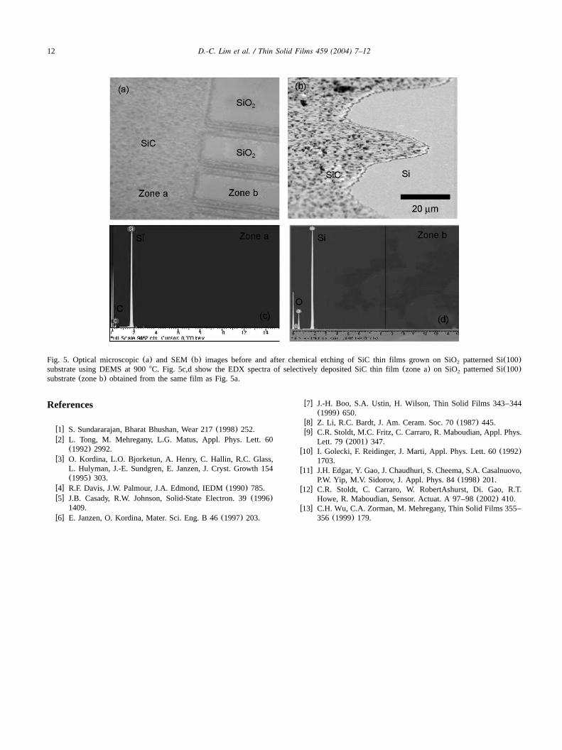
cross-sectional view TEM micrographs is believed to beassociated with mass contrast due to surface roughnessandyor misoriented or twinned regions surrounding theepitaxial growthw10x. The thickness of the SiC film isapproximately 150 nm. Also, the SiC film has verysharp interface and high dense crystal structure. In theTED, besides the normal diffraction pattern due to thecubic structure, extra pattern can be seen indicating theexistence of microtwins and stacking faults caused bythe lattice dismatch between the SiC film and the Si(100) substrate.Fig. 5a shows the optical microscopic image of a
3C–SiC thin film grown on a SiO patterned Si(100)2
surface at 9008C. With conventional high-temperatureCVD method, SiC films deposited on SiO patterned2
Si(100) substrate have larger grain size and roughertexture and become subsequently more porous than filmsgrown on Si(100). As a result, the SiC films on SiO2mask is more readily etched away in concentrated HFsolutionw11–13x while the SiC film on the Si(100) sideis not clearly etched and etching takes a long time.Therefore we have selectively deposited the 3C–SiCthin film on SiO patterned Si(100) surface which2
11D.-C. Lim et al. / Thin Solid Films 459 (2004) 7–12
Fig. 4. AFM images SiC thin films grown on both Si(100) (a) andSiO patterned Si(100) (b) substrates using DEMS at 9008C. Fig.2
4b shows TEM images of the same SiC thin film as Fig. 4a. Theinsert of Fig. 4a shows TED pattern of the same film.
made by UV-dry etching of a mask shielded SiO layers2
after a PR coating of the oxidized Si(100) substrate. InFig. 5a, we could clearly see the selective deposited SiCfilm with more rough surface than that of the SiO2
surface. To confirm this selectivity characteristic onSiO patterned Si(100) substrate, we measure the EDX2
(see Fig. 5c,d). Si and C species were detected in thezone a while Si and O species were only detected inzone b. Carbon species contributed to SiC was notdetected in zone b. From these results, we could derivethat the SiC film was deposited selectively on the SiO2
patterned Si(100) substrate. Therefore, we could etchaway the SiO layer more easily and get the deposited2
SiC film only by lifting off the SiO from the Si(100)2
substrate, suggesting good MEMS applications. Fig. 5bshows the SEM images of SiC thin film after SiO2pattern etched away using HF solution. Also, we meas-ured the hardness of SiC thin films using the microknoop hardness tester. Independently the depositiontemperature, the SiC thin films grown under the samedeposition conditions have high hardness approximately32 GPa.
4. Conclusions
We have deposited the 3C–SiC thin films with highhardness of 32 GPa on Si(100) surfaces by a diethyl-methylsilane(DEMS) single precursor at temperaturesin the range 700–10008C and 1.0=10 Torr fory5
MEMS applications. With increasing the depositiontemperature to 9008C, relatively well oriented 3C–SiClayers were obtained. At this deposition condition, themajor crystal form of 3C–SiC thin film was rectangularin shape on the substrate, and the average crystal sizeand the value of RMS surface roughness are approxi-mately 0.1mm and;32 nm, respectively. Otherwise,the 3C–SiC thin film grown on SiO patterned Si(100)2
substrate has more small crystal size and smooth surfacewith RMS roughness value approximately 6 nm. Withincreasing deposition time from 2 h to 4 h, the crystalsize as well as RMS roughness value also increased.These results show that the deposition temperature andtime could be one of the important factors for influenc-ing the film crystallinity. The XPS result shows that theSiC film grown at 9008C has a slightly carbon rich.We have also selectively deposited cubic silicon carbidethin films on SiO patterned Si(100) substrates. In2
conclusion, the low-temperature chemical vapor depo-sition process using a single precursor for both eptixialSiC growth on Si(100) and selective SiC deposition onSiO patterned Si(100) substrates described in this study2
will be readily adaptable to current MEMS applications.
Acknowledgments
Support of this research by the Ministry of ScienceTechnology in Korea(project No. M10214000278-02B1500-04211) is gratefully acknowledged.
12 D.-C. Lim et al. / Thin Solid Films 459 (2004) 7–12
Fig. 5. Optical microscopic(a) and SEM(b) images before and after chemical etching of SiC thin films grown on SiO patterned Si(100)2
substrate using DEMS at 9008C. Fig. 5c,d show the EDX spectra of selectively deposited SiC thin film(zone a) on SiO patterned Si(100)2
substrate(zone b) obtained from the same film as Fig. 5a.
References
w1x S. Sundararajan, Bharat Bhushan, Wear 217(1998) 252.w2x L. Tong, M. Mehregany, L.G. Matus, Appl. Phys. Lett. 60
(1992) 2992.w3x O. Kordina, L.O. Bjorketun, A. Henry, C. Hallin, R.C. Glass,
L. Hulyman, J.-E. Sundgren, E. Janzen, J. Cryst. Growth 154(1995) 303.
w4x R.F. Davis, J.W. Palmour, J.A. Edmond, IEDM(1990) 785.w5x J.B. Casady, R.W. Johnson, Solid-State Electron. 39(1996)
1409.w6x E. Janzen, O. Kordina, Mater. Sci. Eng. B 46(1997) 203.
w7x J.-H. Boo, S.A. Ustin, H. Wilson, Thin Solid Films 343–344(1999) 650.
w8x Z. Li, R.C. Bardt, J. Am. Ceram. Soc. 70(1987) 445.w9x C.R. Stoldt, M.C. Fritz, C. Carraro, R. Maboudian, Appl. Phys.
Lett. 79 (2001) 347.w10x I. Golecki, F. Reidinger, J. Marti, Appl. Phys. Lett. 60(1992)
1703.w11x J.H. Edgar, Y. Gao, J. Chaudhuri, S. Cheema, S.A. Casalnuovo,
P.W. Yip, M.V. Sidorov, J. Appl. Phys. 84(1998) 201.w12x C.R. Stoldt, C. Carraro, W. RobertAshurst, Di. Gao, R.T.
Howe, R. Maboudian, Sensor. Actuat. A 97–98(2002) 410.w13x C.H. Wu, C.A. Zorman, M. Mehregany, Thin Solid Films 355–
356 (1999) 179.