Embed Size (px)
Citation preview
Delay Calculations
Section 6.1-6.4
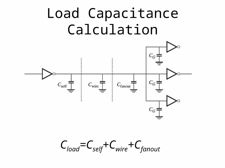
Load Capacitance Calculation
Cload=Cself+Cwire+Cfanout
Fanout Capacitance
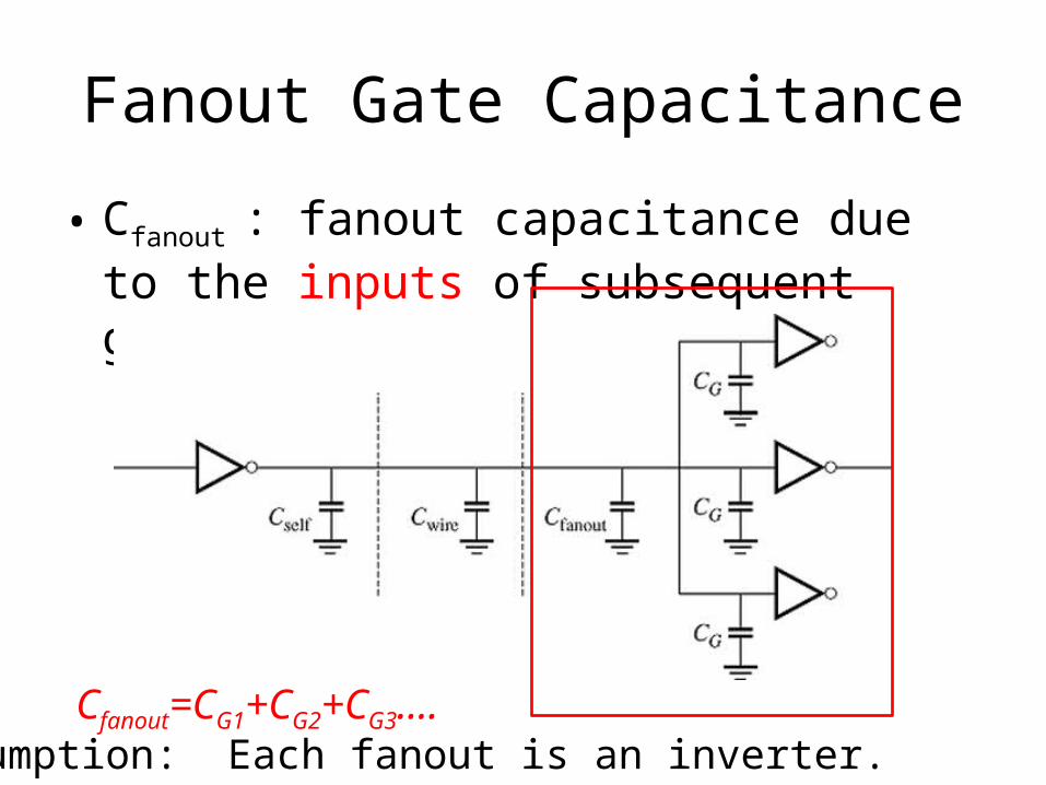
Fanout Gate Capacitance
• Cfanout : fanout capacitance due to the inputs of subsequent gates, CG.
Cfanout=CG1+CG2+CG3….Assumption: Each fanout is an inverter.
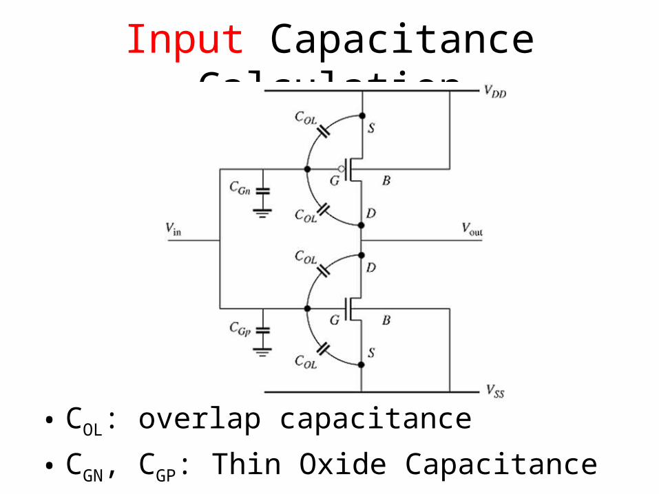
Input Capacitance Calculation
• COL: overlap capacitance
• CGN, CGP: Thin Oxide Capacitance
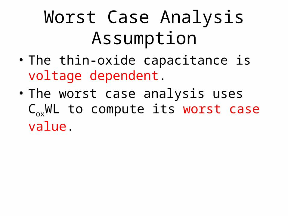
Worst Case Analysis Assumption
• The thin-oxide capacitance is voltage dependent.
• The worst case analysis uses CoxWL to compute its worst case value.
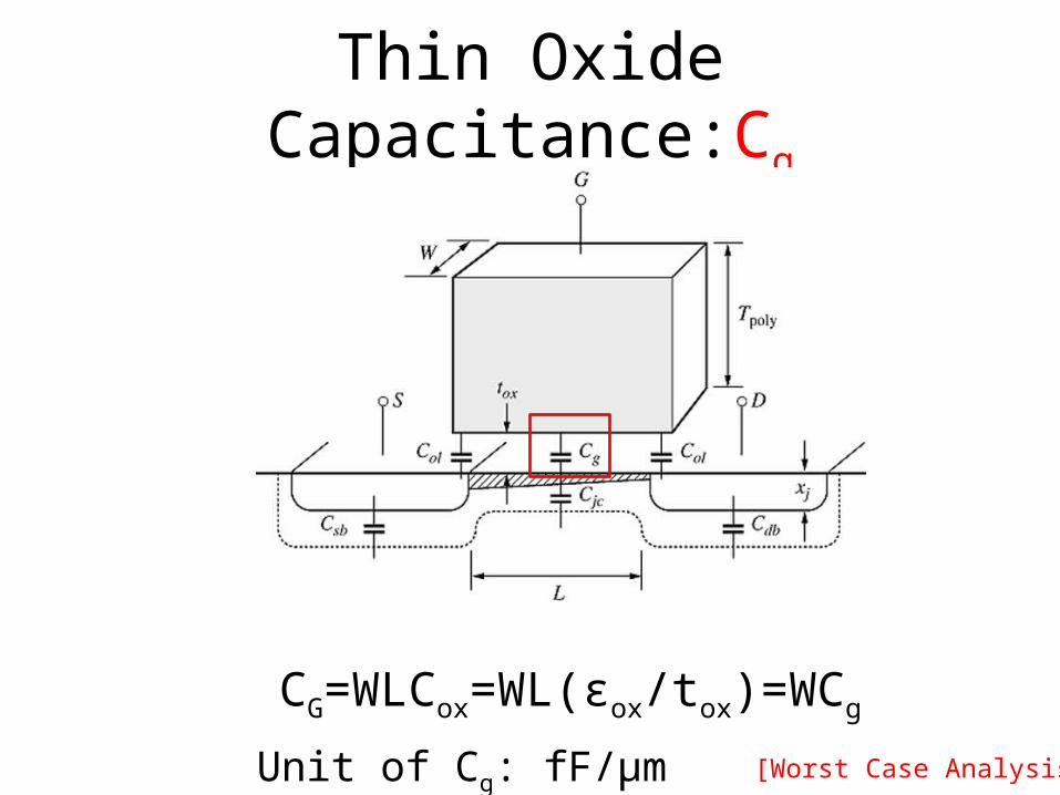
Thin Oxide Capacitance:Cg
CG=WLCox=WL(εox/tox)=WCg
Unit of Cg: fF/μm [Worst Case Analysis]
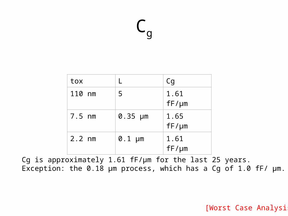
Cg
tox L Cg
110 nm 5 1.61 fF/μm
7.5 nm 0.35 μm 1.65 fF/μm
2.2 nm 0.1 μm 1.61 fF/μm
Cg is approximately 1.61 fF/μm for the last 25 years.Exception: the 0.18 μm process, which has a Cg of 1.0 fF/ μm.
[Worst Case Analysis]
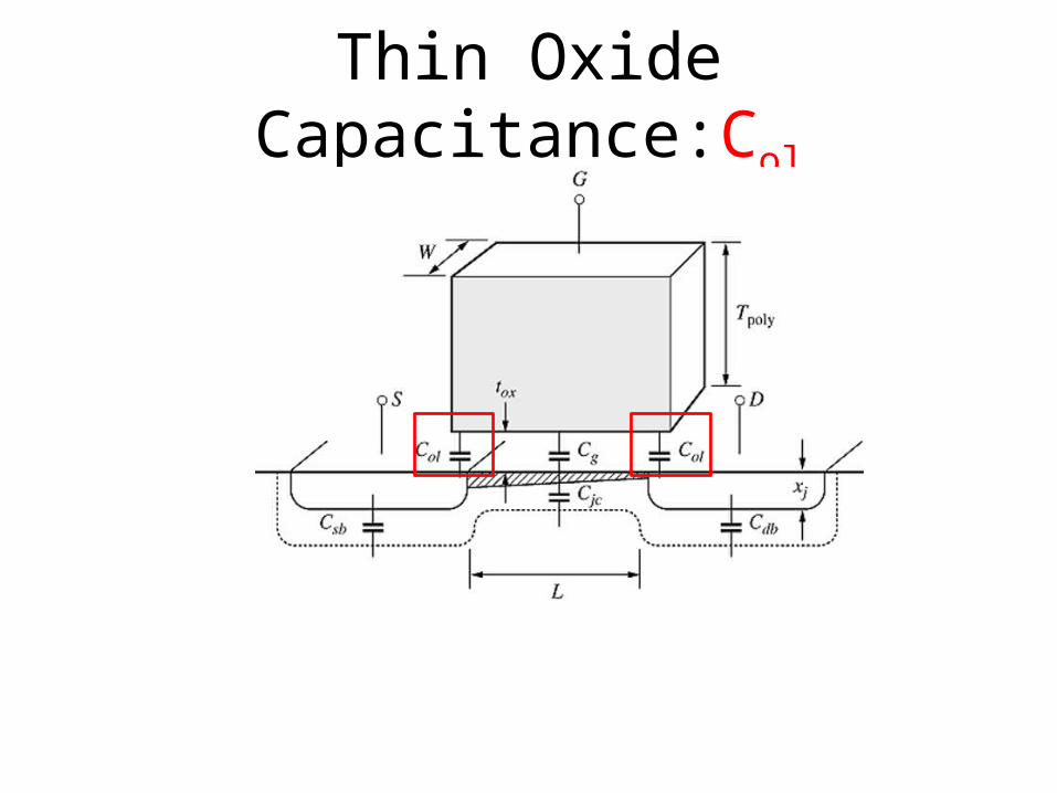
Thin Oxide Capacitance:Col
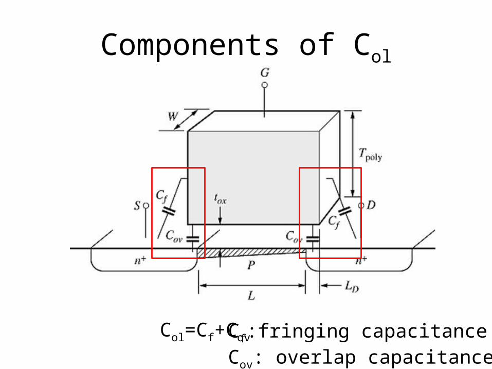
Components of Col
Col=Cf+Cov Cf:fringing capacitanceCov: overlap capacitance
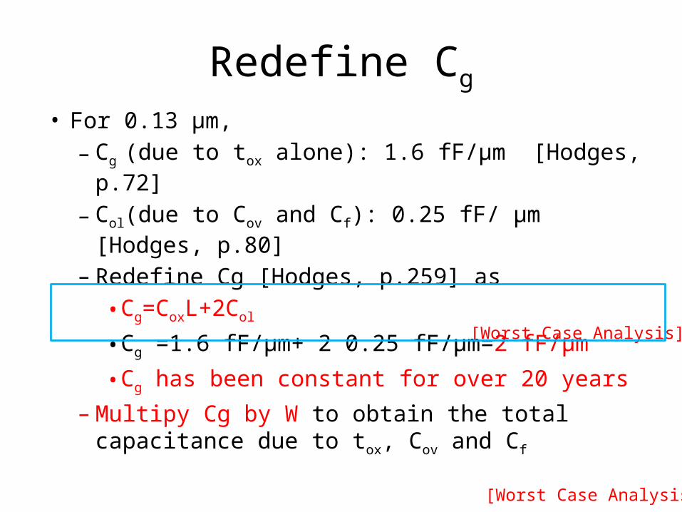
Redefine Cg
• For 0.13 μm,– Cg (due to tox alone): 1.6 fF/μm [Hodges, p.72]
– Col(due to Cov and Cf): 0.25 fF/ μm [Hodges, p.80]– Redefine Cg [Hodges, p.259] as• Cg=CoxL+2Col
• Cg =1.6 fF/μm+ 2 0.25 fF/μm=2 fF/μm
• Cg has been constant for over 20 years– Multipy Cg by W to obtain the total capacitance
due to tox, Cov and Cf
[Worst Case Analysis]
[Worst Case Analysis]
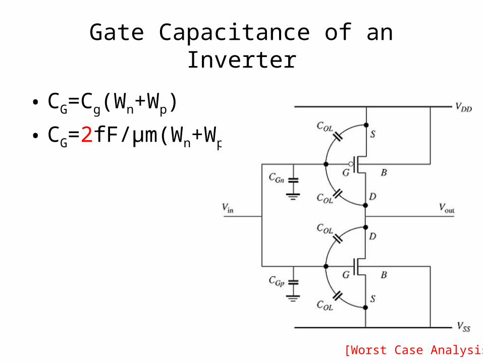
Gate Capacitance of an Inverter
• CG=Cg(Wn+Wp)
• CG=2fF/μm(Wn+Wp)
[Worst Case Analysis]
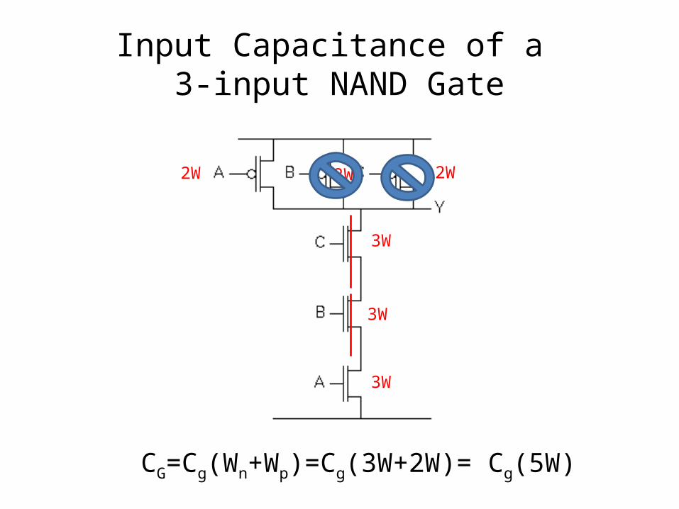
Input Capacitance of a 3-input NAND Gate
2W 2W 2W
3W
3W
3W
CG=Cg(Wn+Wp)=Cg(3W+2W)= Cg(5W)
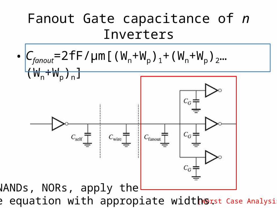
Fanout Gate capacitance of n Inverters
• Cfanout=2fF/μm[(Wn+Wp)1+(Wn+Wp)2…(Wn+Wp)n]
[Worst Case Analysis]
For NANDs, NORs, apply the above equation with appropiate widths.
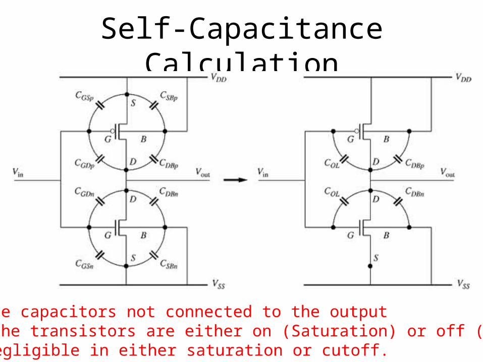
Self-Capacitance Calculation
1. Eliminate capacitors not connected to the output2. Assume the transistors are either on (Saturation) or off (Cutoff). 3. CGD is negligible in either saturation or cutoff.
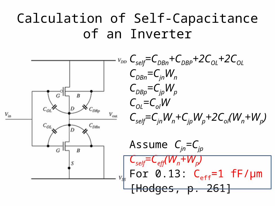
Calculation of Self-Capacitance of an Inverter
Cself=CDBn+CDBP+2COL+2COL
CDBn=CjnWn
CDBp=CjpWp
COL=ColWCself=CjnWn+CjpWp+2Col(Wn+Wp)
Assume Cjn=Cjp
Cself=Ceff(Wn+Wp)For 0.13: Ceff=1 fF/μm [Hodges, p. 261]
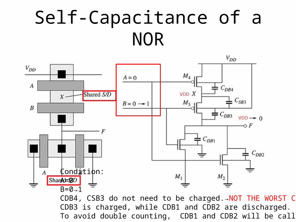
Self-Capacitance of a NOR
Condition:A=0B=0→1CDB4, CSB3 do not need to be charged.→NOT THE WORST CASECDB3 is charged, while CDB1 and CDB2 are discharged.To avoid double counting, CDB1 and CDB2 will be called CDB12.
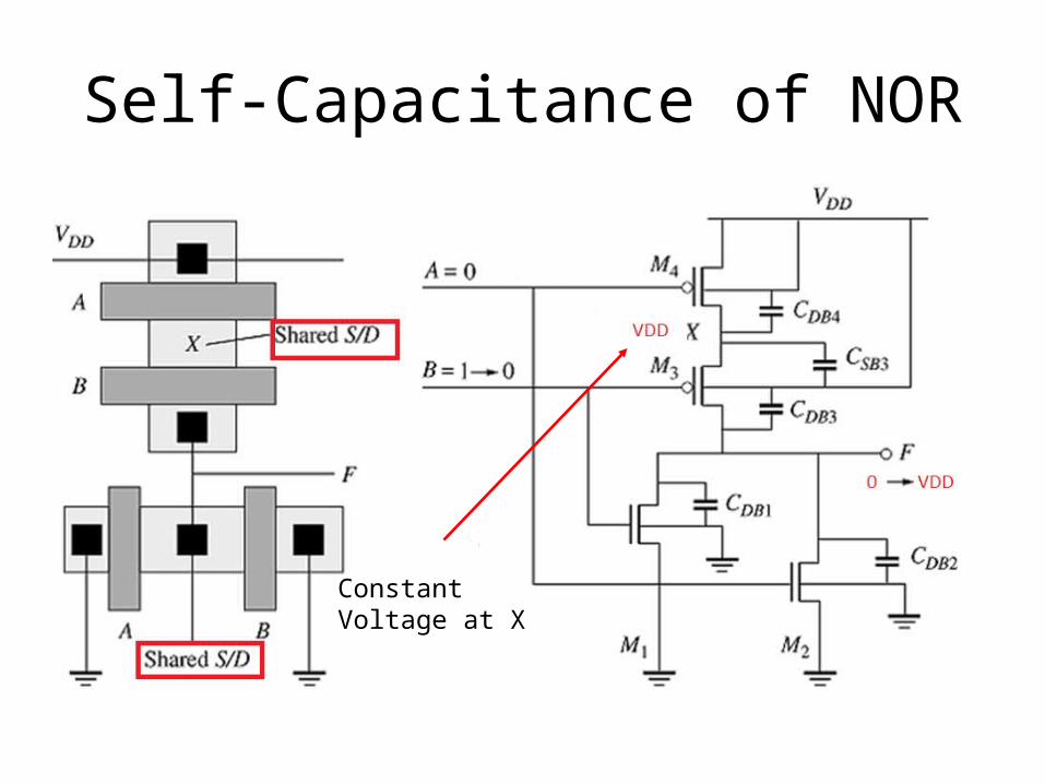
Self-Capacitance of NOR
Constant Voltage at X
Self-Capacitance of a NOR
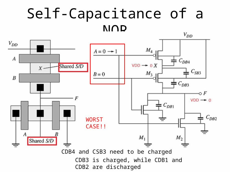
CDB4 and CSB3 need to be chargedCDB3 is charged, while CDB1 and CDB2 are discharged
WORST CASE!!
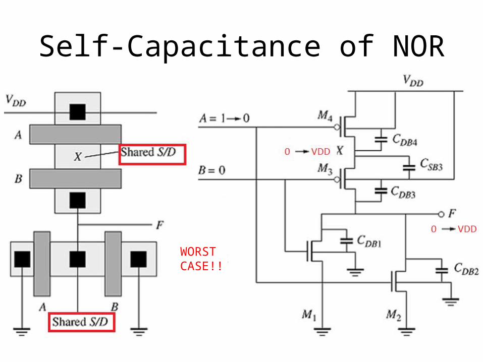
Self-Capacitance of NOR
WORST CASE!!
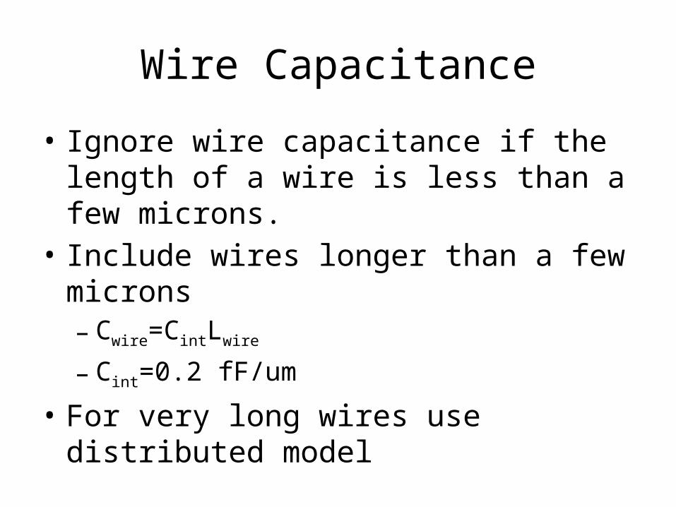
Wire Capacitance
• Ignore wire capacitance if the length of a wire is less than a few microns.
• Include wires longer than a few microns– Cwire=CintLwire
– Cint=0.2 fF/um
• For very long wires use distributed model
Example 6.4
• Capacitance Calculation for Inverter
Propagation Delay
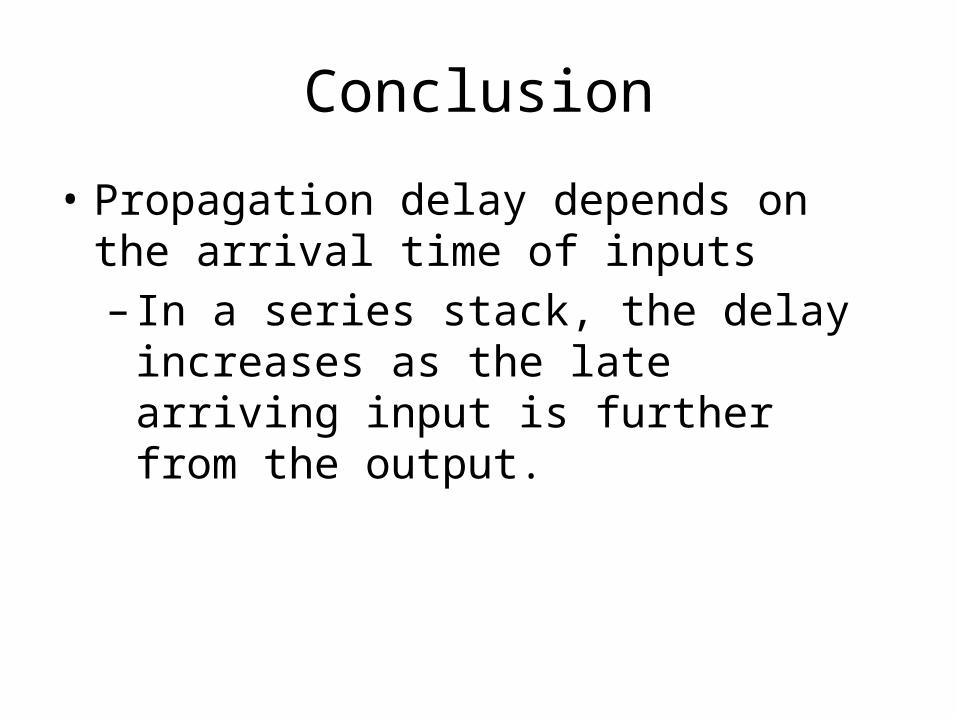
Conclusion
• Propagation delay depends on the arrival time of inputs– In a series stack, the delay increases as the
late arriving input is further from the output.
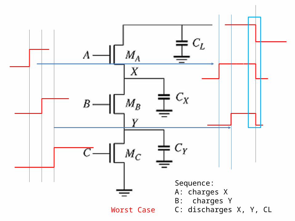
Sequence:A: charges XB: charges YC: discharges X, Y, CLWorst Case
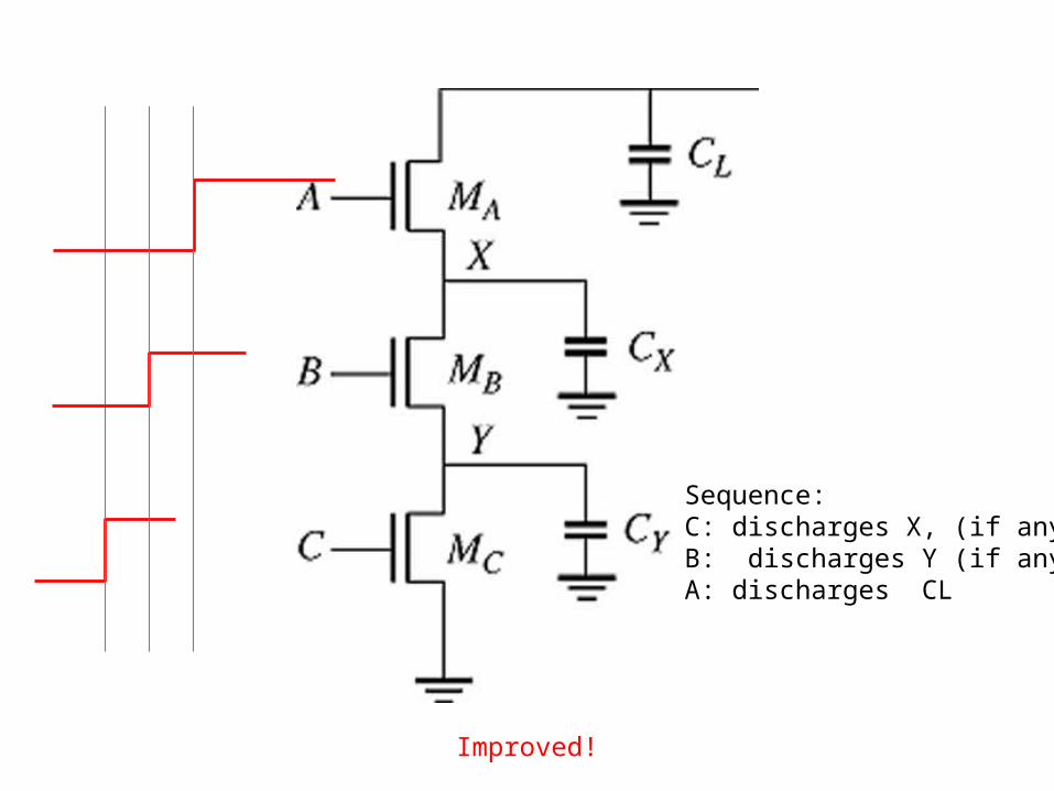
Sequence:C: discharges X, (if any)B: discharges Y (if any)A: discharges CL
Improved!
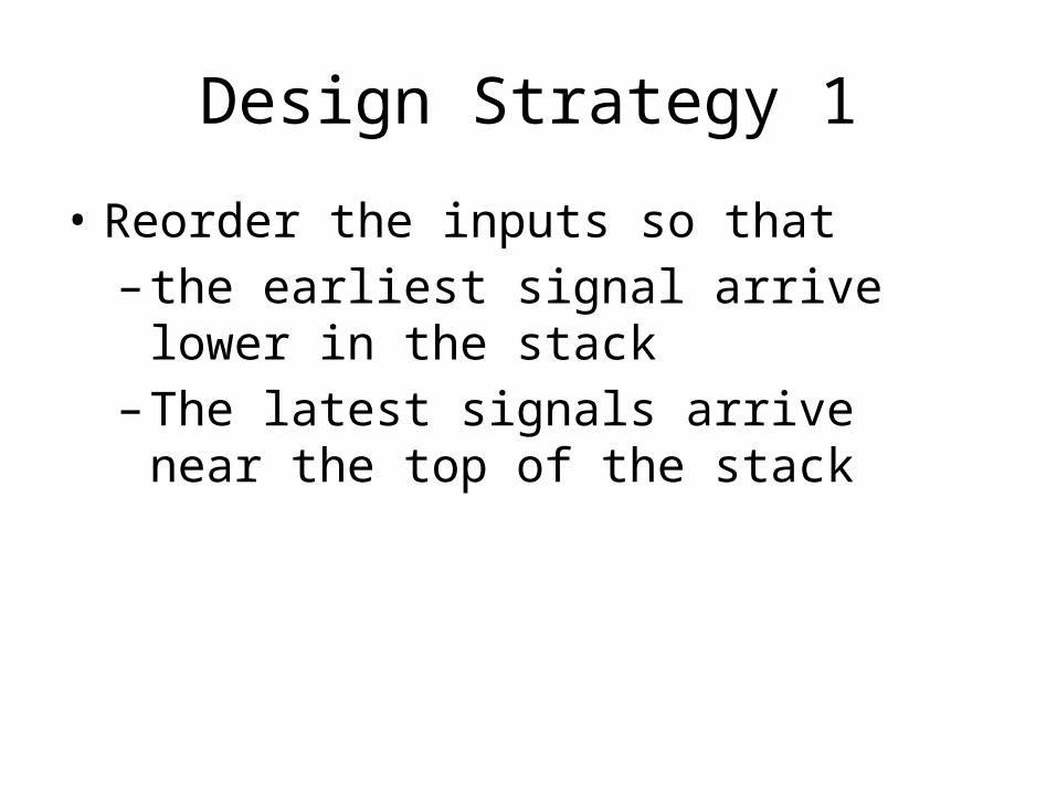
Design Strategy 1
• Reorder the inputs so that – the earliest signal arrive lower in the stack – The latest signals arrive near the top of the
stack
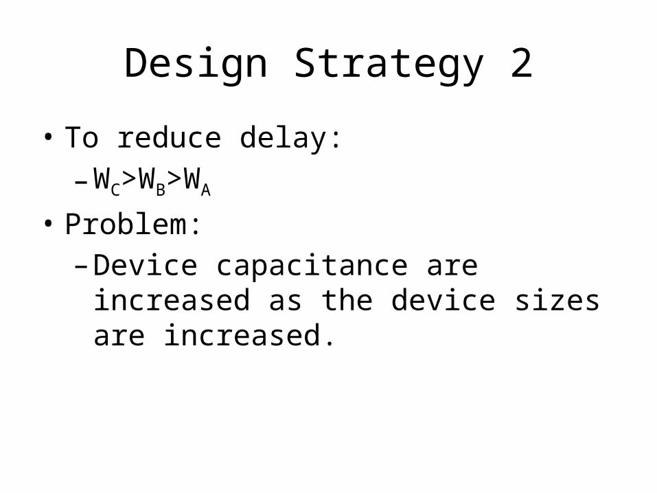
Design Strategy 2
• To reduce delay:–WC>WB>WA
• Problem:–Device capacitance are increased as the
device sizes are increased.
Delay Calculation with Input Slope
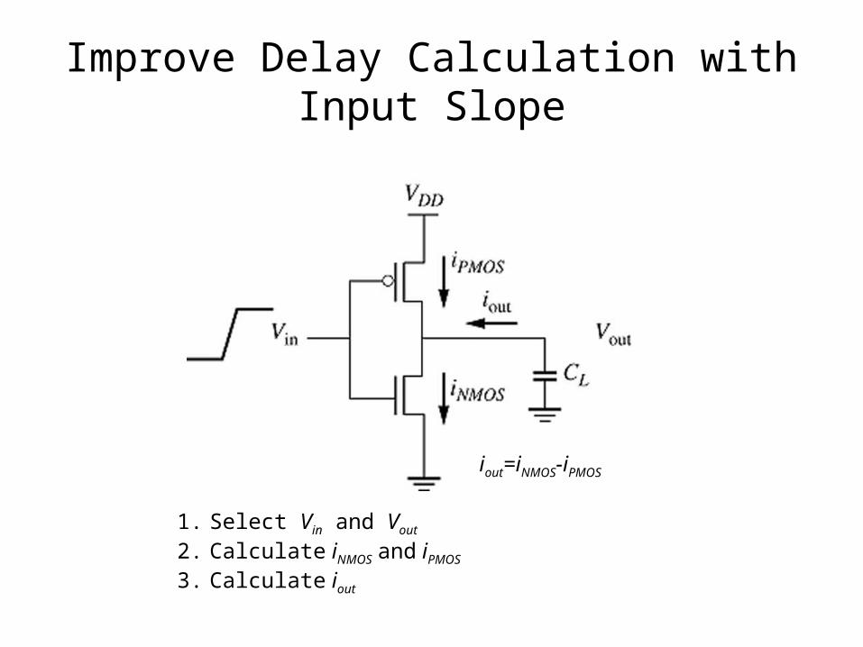
Improve Delay Calculation with Input Slope
iout=iNMOS-iPMOS
1. Select Vin and Vout
2. Calculate iNMOS and iPMOS
3. Calculate iout
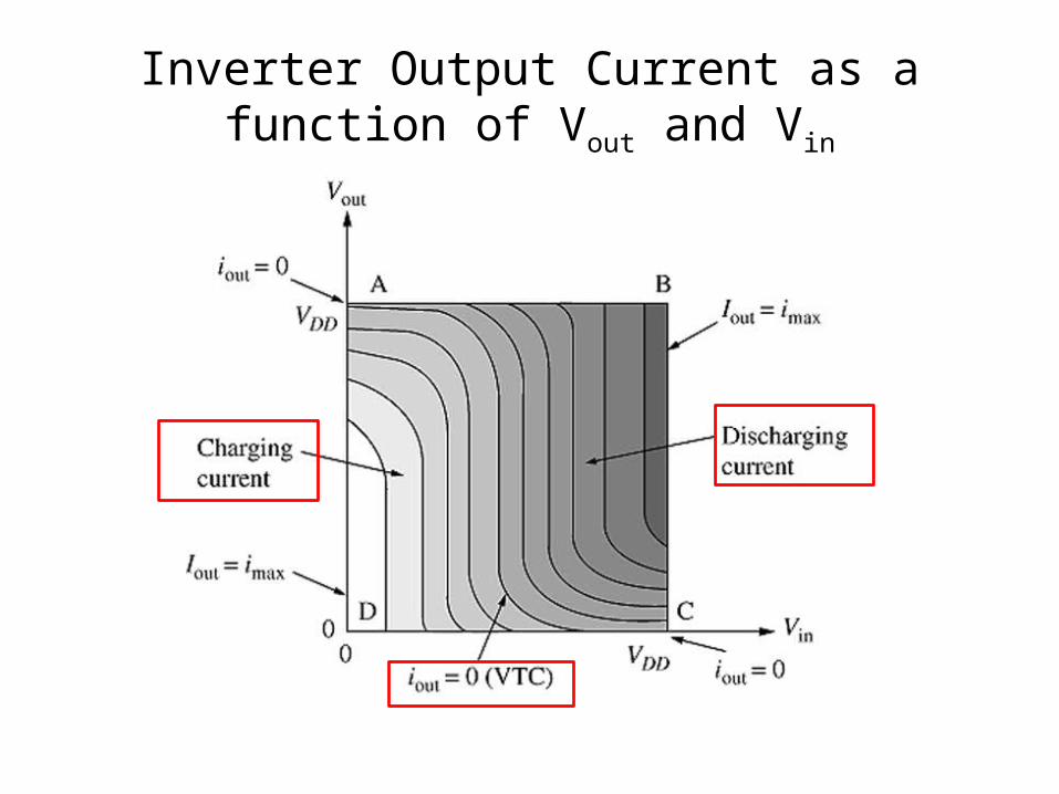
Inverter Output Current as a function of Vout and Vin
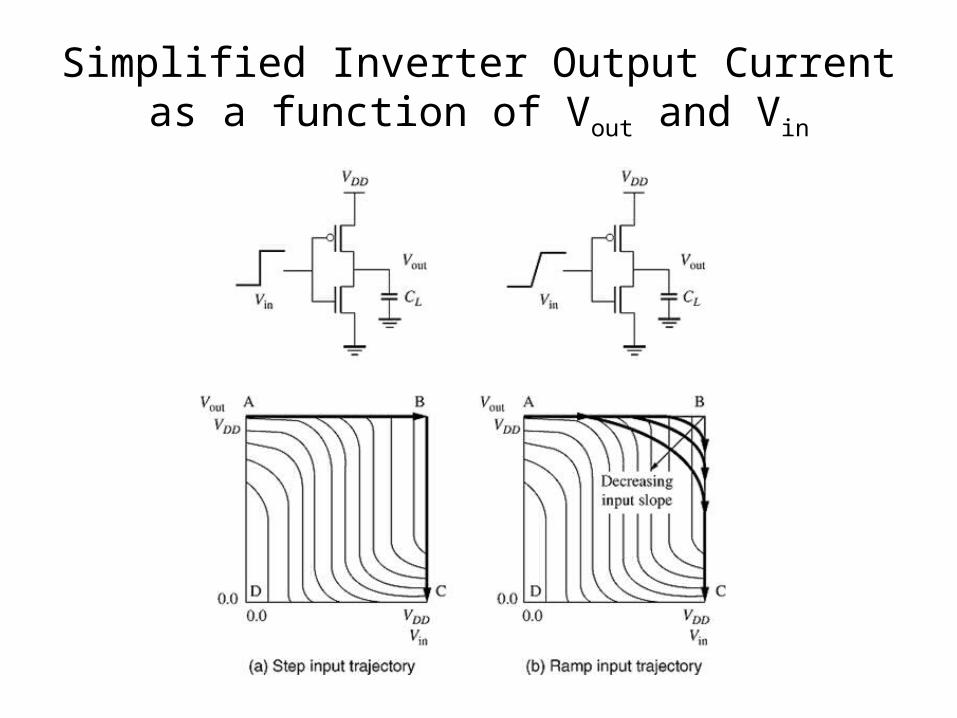
Simplified Inverter Output Current as a function of Vout and Vin
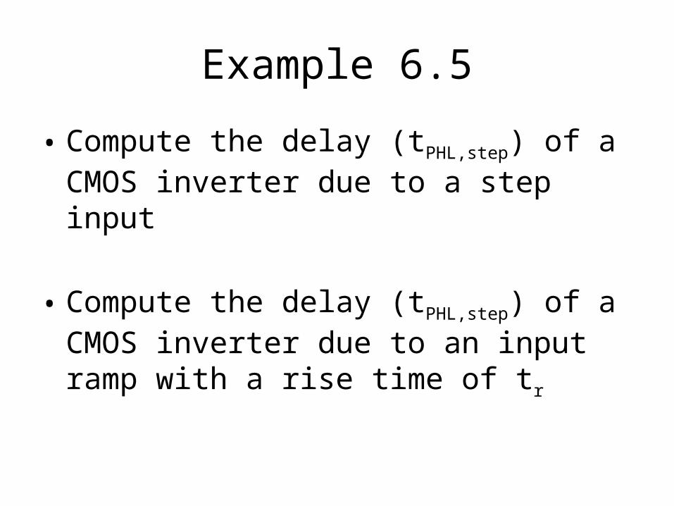
Example 6.5
• Compute the delay (tPHL,step) of a CMOS inverter due to a step input
• Compute the delay (tPHL,step) of a CMOS inverter due to an input ramp with a rise time of tr
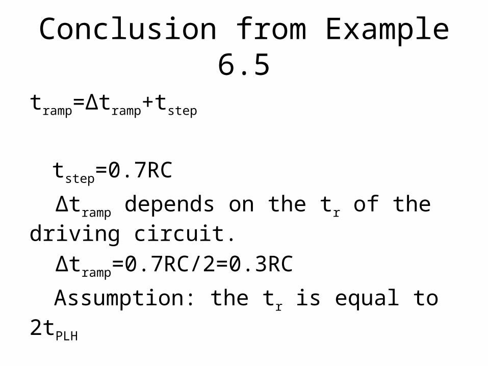
Conclusion from Example 6.5
tramp=Δtramp+tstep
tstep=0.7RC
Δtramp depends on the tr of the driving circuit.
Δtramp=0.7RC/2=0.3RC
Assumption: the tr is equal to 2tPLH
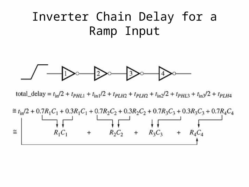
Inverter Chain Delay for a Ramp Input
Example 6.6