Embed Size (px)
Citation preview

www.rohm.com 2009.09 - Rev.B© 2009 ROHM Co., Ltd. All rights reserved.
1/18
Memory for Plug & Play
DDR/DDR2 (For memory module) SPD Memory
BR34E02FVT-W,BR34E02NUX-W Description
BR34E02FVT-W is 256×8 bit Electrically Erasable PROM (Based on Serial Presence Detect)
Features 1) 256×8 bit architecture serial EEPROM 2) Wide operating voltage range: 1.7V-3.6V 3) Two-wire serial interface 4) High reliability connection using Au pads and Au wires 5) Self-Timed Erase and Write Cycle 6) Page Write Function (16byte) 7) Write Protect Mode
Settable Reversible Write Protect Function: 00h-7Fh Write Protect 1 (Onetime Rom) : 00h-7Fh Write Protect 2 (Hardwire WP PIN) : 00h-FFh
8) Low Power consumption Write (at 1.7V ) : 0.4mA (typ.) Read (at 1.7V ) : 0.1mA(typ.) Standby ( at 1.7V ) : 0.1µA(typ.)
9) DATA security Write protect feature (WP pin) Inhibit to WRITE at low VCC
10) Compact package: TSSOP-B8, VSON008X2030 11) High reliability fine pattern CMOS technology 12) Rewriting possible up to 1,000,000 times 13) Data retention: 40 years 14) Noise reduction Filtered inputs in SCL / SDA 15) Initial data FFh at all addresses
BR34E02-W Series
Capacity Bit format Type Power Source Voltage TSSOP-B8 VSON008X2030 2Kbit 256X8 BR34E02-W 1.7V~3.6V
Absolute Maximum Ratings (Ta=25)
Parameter Symbol Rating Unit Supply Voltage VCC -0.3~+6.5 V
Power Dissipation Pd 330(BR34E02FVT-W) *1
mW 300(BR34E02NUX-W) *2
Storage Temperature Tstg -65~+125 Operating Temperature Topr -40~+85 Terminal Voltage (A0) - -0.3~10.0 V Terminal Voltage (etcetera) - -0.3~VCC+0.3 V * Reduce by 3.3mW(*1), 3.0 mW(*2)/C over 25C
Recommended operating conditions
Parameter Symbol Rating Unit Supply Voltage VCC 1.7~3.6 V Input Voltage VIN 0~VCC V
No.09002EBT03

BR34E02FVT-W, BR34E02NUX-W Technical Note
www.rohm.com 2009.09 - Rev.B© 2009 ROHM Co., Ltd. All rights reserved.
2/18
Memory cell characteristics(Ta=25, VCC=1.7V~3.6V)
Parameter Specification
Unit Min. Typ. Max.
Write / Erase Cycle *1 1,000,000 - - Cycles Data Retention *1 40 - - Years *1:Not 100% TESTED
Electrical characteristics - DC(Unless otherwise specified Ta=-40~+85, VCC=1.7V~3.6V)
Parameter Symbol Specification
Unit Test Condition Min. Typ. Max.
"H" Input Voltage VIH1 0.7 VCC - Vcc+0.3 V "L" Input Voltage VIL1 - - 0.3 VCC V "L" Output Voltage 1 VOL1 -0.3 - 0.4 V IOL=2.1mA,2.5V≦VCC≦3.6V(SDA) "L" Output Voltage 2 VOL2 - - 0.2 V IOL=0.7mA,1.7V≦VCC<2.5V(SDA) Input Leakage Current 1 ILI1 -1 - 1 µA VIN=0V~VCC(A0,A1,A2,SCL) Input Leakage Current 2 ILI2 -1 - 15 µA VIN=0V~VCC(WP) Input Leakage Current 3 ILI3 -1 - 20 µA VIN=VHV(A0) Output Leakage Current ILO -1 - 1 µA VOUT=0V~VCC
Operating Current
ICC1 - - 1.0 mA
VCC=1.7V,fSCL=100kHz,tWR=5ms Byte Write Page Write Write Protect
ICC2 - - 3.0 mA
VCC =3.6V,fSCL=100kHz, tWR=5ms Byte Write Page Write Write Protect
ICC3 - - 0.5 mA
VCC =3.6V,fSCL=100kHz Random Read Current Read Sequential Read
Standby Current ISB - - 2.0 µAVCC =3.6V,SDA,SCL= VCC A0,A1,A2=GND,WP=GND
A0 HV Voltage VHV 7 - 10 V VHV-Vcc≧4.8V Note: This IC is not designed to be radiation-resistant.
lectrical characteristics - AC(Unless otherwise specified Ta=-40~+85, VCC =1.7V~3.6V)
Parameter Symbol FAST-MODE
2.5V≦VCC≦5.5V STANDARD-MODE 1.7V≦VCC≦5.5V Unit
Min. Typ. Max. Min. Typ. Max. Clock Frequency fSCL - - 400 - - 100 kHz Data Clock High Period tHIGH 0.6 - - 4.0 - - µs Data Clock Low Period tLOW 1.2 - - 4.7 - - µs SDA and SCL Rise Time
*1 tR - - 0.3 - - 1.0 µs
SDA and SCL Fall Time *1 tF - - 0.3 - - 0.3 µs Start Condition Hold Time tHD:STA 0.6 - - 4.0 - - µs Start Condition Setup Time tSU:STA 0.6 - - 4.7 - - µs Input Data Hold Time tHD:DAT 0 - - 0 - - ns Input Data Setup Time tSU:DAT 100 - - 250 - - ns Output Data Delay Time tPD 0.1 - 0.9 0.1 - 3.5 µs Output Data Hold Time tDH 0.1 - - 0.1 - - µs Stop Condition Setup Time tSU:STO 0.6 - - 4.0 - - µs Bus Free Time tBUF 1.2 - - 4.7 - - µs Write Cycle Time tWR - - 5 - - 5 ms Noise Spike Width (SDA and SCL)
tI - - 0.1 - - 0.1 µs
WP Hold Time tHD:WP 0 - - 0 - - ns WP Setup Time tSU:WP 0.1 - - 0.1 - - µs WP High Period tHIGH:WP 1.0 - - 1.0 - - µs
*1:Not 100% TESTED
BR34E02FVT-W, BR34E02NUX-W Technical Note
www.rohm.com 2009.09 - Rev.B© 2009 ROHM Co., Ltd. All rights reserved.
3/18
SDA
SCL
D0 ACK
STOP CONDITION START CONDITION
tWR WRITE DATA(n)
Fast / Standard Modes Fast mode and Standard mode differ only in operation frequency. Operations performed at 100kHz are considered in "Standard-mode", while those conducted at 400kHz are in "Fast-mode". Please note that these clock frequencies are maximum values. At lower power supply voltage it is difficult to operate at high speeds. The EEPROM can operate at 400kHz, between 2.5V and 3.6V, and at 100kHz from 1.7V-2.5V.
Synchronous Data Timing
SCL
SDA
WP
tHD:WP
Stop Condition
tWR
D1 D0 ACK ACK
DATA(1) DATA(n)
tSU:WP
Fig.1-(d) WP Timing Of The Write Operation
SDA (IN)
SDA (OUT)
tHD:STA tHD:DATtSU:DAT
tBUF tPD tDH
tLOW
tHIGH tR tF
SCL
Fig.1-(a) Synchronous Data Timing
SDA data is latched into the chip at the rising edge of SCL clock.
Output data toggles at the falling edge of SCL clock.
SDA
tSU:STA tSU:STO tHD:STA
START BIT STOP BIT
SCL
Fig.1-(b) Start/Stop Bit Timing
tHIGH:WP
WP
SDA D1 D0 ACK ACK
DATA(1) DATA(n)
tWR
SCL
Fig.1-(e) WP Timing Of The Write Cancel Operation
Fig.1-(c) Write Cycle Timing
For WRITE operation, WP must be "Low" from the rising edge of the clock (which takes in D0 of first byte) until the end of tWR. (See Fig.1-(d) ) During this period, WRITE operation can be canceled by setting WP "High".(See Fig.1-(e))
When WP is set to "High" during tWR, WRITE operation is immediately ceased, making the data unreliable. It must then be re-written.

BR34E02FVT-W, BR34E02NUX-W Technical Note
www.rohm.com 2009.09 - Rev.B© 2009 ROHM Co., Ltd. All rights reserved.
4/18
*1 Open drain output requires a pull-up resistor. *2 WP Pin has a Pull-Down resistor. Please leave unconnected or connect to GND when not in use.
Fig.7 "L" Output Voltage VOL2-IOL2 (VCC=1.7V)
8
7
6
5 4
3
2
1
SDA
SCL
WP
VCC
GND
A2
A1
A0
ADDRESS
DECODER SLAVE , WORD
ADDRESS
GS
DATA
REGISTE
CONTOROL LOGIC
HIGH VOLTAGE VCC LEVEL
8bit
8bit
8bit
ACK
START STOP
PROTECT_MEMORY_ARRY
2Kbit_MEMORY_ARRY
Block diagram
Pinout diagram and description
Pin Name Input/Output Functions
VCC - Power Supply
GND - Ground 0V
A0,A1,A2 IN Slave Address Set.
SCL IN Serial Clock Input
SDA IN / OUT Slave and Word Address, *1
Serial Data Input, Serial Data Output
WP IN Write Protect Input *2
Electrical characteristics curves
The following characteristic data are typ. value.
Fig.6 "L" Output Voltage VOL1-IOL1 (VCC=2.5V)
Fig.8 Input Leakage Current ILI1 (A0,A1,A2,SCL,SDA)
Fig.9 Input Leakage Current ILI2 (WP)
8
7
6
5
1
2
3
4
V CC
WP
SCL
SDA
A0
A1
A2
GND
Fig.3 Pin Configuration
BR34E02FVT-W
BR34E02NUX-W
Fig.5 "L" Input Voltage VIL (A0,A1,A2,SCL,SDA,WP)
Fig.4 "H" Input Voltage VIH (A0,A1,A2,SCL,SDA,WP)
Fig.2 Blo
0
0.2
0.4
0.6
0.8
1
0 1 2 3 4
IOL1[mA]
VO
L1[V
]
Ta=85
SPEC
Ta=25
Ta=-40 0
1
2
3
4
5
6
0 1 2 3 4
VCC[V]
VIL
1,2[
V]
Ta=85 Ta=-40 Ta=25
SPEC
0
0.2
0.4
0.6
0.8
1
0 1 2 3 4
IOL2[mA]
VO
L2[V
]
Ta=85
SPEC Ta=25
Ta=-40
0
0.2
0.4
0.6
0.8
1
1.2
0 1 2 3 4
VCC[V]
ILI1
[μA
]
Ta=85 Ta=25 Ta=-40
SPEC
0
4
8
12
16
0 1 2 3 4
VCC[V]
ILI2
[μA
]
Ta=85 Ta=25 Ta=-40
SPEC
SPEC
Ta=85 Ta=-40 Ta=25

BR34E02FVT-W, BR34E02NUX-W Technical Note
www.rohm.com 2009.09 - Rev.B© 2009 ROHM Co., Ltd. All rights reserved.
5/18
-200
-100
0
100
200
300
0 1 2 3 4
VCC[V]
tSU
:DA
T(L
OW
)[ns
]
0
0.5
1
1.5
2
2.5
0 1 2 3 4
VCC[V]
ISB
[μA
]
Fig.10 Write Operating Current ICC1,2 (fSCL=100kHz,400kHz)
Fig.15 Data Clock Low Period tLow
Fig.11 Read Operating Current ICC3 (fSCL=400kHz)
Fig.13 Clock Frequency fSCL
Fig.17 Start Condition Setup Time tSU:STA
Fig.12 Standby Current ISB
Fig.14 Data Clock High Period tHigh
Fig.19 Data Hold Time tHD:DAT(LOW)
Fig.21 Input Data Setup Time tSU:DAT(LOW)
Fig.16 Start Condition Hold Time tHD:STA
0
0.1
0.2
0.3
0.4
0.5
0.6
0 1 2 3 4
VCC[V]
ICC
3[m
A]
SPEC
Ta=85 Ta=25
fSCL=100kHz DATA=AAh
0
0.5
1
1.5
2
2.5
3
3.5
0 1 2 3 4
VCC[V]
ICC
1,2
[mA
]
SPEC1
fSCL=400kHz(VCC≧2.5V) fSCL=100kHz(1.7V≦Vcc<2.5V) DATA=AA
Ta=25 Ta=85
Ta=-40
Ta=-40
SPEC
Ta=85 Ta=25
0
1
2
3
4
5
0 1 2 3 4
VCC[V]
tHIG
H[μ
s]
Ta=-40
SPEC2
Ta=85 Ta=25
SPEC1
SPEC1:FAST-MODE SPEC2:STANDARD-MODE
1
10
100
1000
10000
0 1 2 3 4
VCC[V]
fSC
L[kH
z]
Ta=-40
SPEC1
Ta=85 Ta=25
SPEC2
SPEC1:FAST-MODE SPEC2:STANDARD-MODE
0
1
2
3
4
5
0 1 2 3 4
VCC[V]
tLO
W[μ
s]
SPEC2
Ta=-40
Ta=85 Ta=25
SPEC1
SPEC1:FAST-MODE SPEC2:STANDARD-MODE
FiagmDag.18 ck DiTarata HoldimtHD:DAT(High)
-200
-150
-100
-50
0
50
0 1 2 3 4
VCC[V]
tHD
:DA
T(H
IGH
)[μ
s]
SPEC1,2
Ta=-40
=85 Ta=25
SPEC1:FAST-MODE SPEC2:STANDARD-MODE
0
1
2
3
4
5
0 1 2 3 4
VCC[V]
tHD
:ST
A[μ
s]
Ta=-40
SPEC2
Ta=85 Ta=25
SPEC1
SPEC1:FAST-MODE SPEC2:STANDARD-MODE
-200
-100
0
100
200
300
0 1 2 3 4
VCC[V]
tSU
:DA
T(H
IGH
)[n
s]
0
1
2
3
4
5
0 1 2 3 4
VCC[V]
tSU
:ST
A[μ
s]
Ta=-40
SPEC2
Ta=85 Ta=25
SPEC1
SPEC1:FAST-MODE SPEC2:STANDARD-MODE
SPEC1
Ta=85 Ta=-40 Ta=25
SPEC1:FAST-MODE SPEC2:STANDARD-MODE
SPEC2
Ta=85
Ta=-40 Ta=25
SPEC1:FAST-MODE SPEC2:STANDARD-MODE
-200
-150
-100
-50
0
50
0 1 2 3 4
VCC[V]
tHD
:DA
T(L
OW
)[μ
s]
SPEC1,2
Ta=-40
Ta=85
Ta=25
SPEC1:FAST-MODE SPEC2:STANDARD-MODE
Fig.20 Input Data Setup Time tSU:DAT(HIGH)
SPEC2
SPEC1
SPEC2
Ta=40

BR34E02FVT-W, BR34E02NUX-W Technical Note
www.rohm.com 2009.09 - Rev.B© 2009 ROHM Co., Ltd. All rights reserved.
6/18
Fig.24 Stop Condition Setup Time tSU:STO
Fig.25 Bus Free Time tBUF
Fig.26 Write Cycle Time tWR
Fig.31 WP Setup Time tSU:WP
Fig.32 WP High Period tHigh:WP
Fig.30 Noise Spike Width tI(SDA L)
Fig.23 Output Data Hold Time tDH
Fig.22 Output Data Delay Time tPD
Fig.29 Noise Spike Width tI(SDA H)
Fig.27 Noise Spike Width tI(SCL H)
Fig.28 Noise Spike Width tI(SCL L)
0
1
2
3
4
0 1 2 3 4
VCC[V]
tDH
[μs]
Ta=85 Ta=-40 Ta=25
SPEC1
SPEC2
SPEC1:FAST-MODE SPEC2:STANDARD-MODE
0
1
2
3
4
0 1 2 3 4
VCC[V]
tPD
[μs ]
SPEC2
Ta=85 Ta=-40 Ta=25 SPEC1
SPEC1
SPEC2
SPEC1:FAST-MODE SPEC2:STANDARD-MODE
0
1
2
3
4
5
0 1 2 3 4
VCC[V]
tSU
:ST
O[μ
s]
SPEC2
Ta=85 Ta=-40
Ta=25 SPEC1
SPEC1:FAST-MODE SPEC2:STANDARD-MODE
0
1
2
3
4
5
0 1 2 3 4
VCC[V]
tBU
F[μ
s]
SPEC2
Ta=85
Ta=-40 Ta=25 SPEC1
SPEC1:FAST-MODE SPEC2:STANDARD-MODE
0
1
2
3
4
5
6
0 1 2 3 4
VCC[V]
tWR
[ms]
SPEC1,2
Ta=85
Ta=-40 Ta=25
SPEC1:FAST-MODE SPEC2:STANDARD-MODE 0
0.1
0.2
0.3
0.4
0.5
0.6
0 1 2 3 4
VCC[V]
tI(S
CL
H)[
μs]
SPEC1,2
Ta=85
Ta=-40
Ta=25
SPEC1:FAST-MODE SPEC2:STANDARD-MODE
0
0.1
0.2
0.3
0.4
0.5
0.6
0 1 2 3 4
VCC[V]
tI(S
CL
L)[
μs]
SPEC1,2
Ta=85
Ta=-40
Ta=25
SPEC1:FAST-MODE SPEC2:STANDARD-MODE
0
0.1
0.2
0.3
0.4
0.5
0.6
0 1 2 3 4
VCC[V]
tI(S
DA
H)[
μs]
SPEC1,2
Ta=85
Ta=-40
Ta=25
SPEC1:FAST-MODE SPEC2:STANDARD-MODE
0
0.1
0.2
0.3
0.4
0.5
0.6
0 1 2 3 4
VCC[V]
tI(S
DA
L)[
μs]
SPEC1,2
Ta=85
Ta=-40 Ta=25
SPEC1:FAST-MODE SPEC2:STANDARD-MODE
-0.6
-0.4
-0.2
0
0.2
0 1 2 3 4
VCC[V]
tSU
:WP
[μs
]
SPEC1,2
Ta=85
Ta=-40
Ta=25
SPEC1:FAST-MODE SPEC2:STANDARD-MODE
0
0.2
0.4
0.6
0.8
1
1.2
0 1 2 3 4
VCC[V]
tHIG
H:W
P[μ
s]
SPEC1,2
Ta=85
Ta=-40
Ta=25
SPEC1:FAST-MODE SPEC2:STANDARD-MODE

BR34E02FVT-W, BR34E02NUX-W Technical Note
www.rohm.com 2009.09 - Rev.B© 2009 ROHM Co., Ltd. All rights reserved.
7/18
Data transfer on the I2C BUS Data transfer on the I2C BUS
The BUS is considered to be busy after the START condition and free a certain time after the STOP condition. Every SDA byte must be 8-bits long and requires an ACKNOWLEDGE signal after each byte. The devices have Master and Slave configurations. The Master device initiates and ends data transfer on the BUS and generates the clock signals in order to permit transfer. The EEPROM in a slave configuration is controlled by a unique address. Devices transmitting data are referred to as the Transmitter. The devices receiving the data are called Receiver.
START Condition (Recognition of the START bit) ・All commands are proceeded by the start condition, which is a High to Low transition of SDA when SCL is High. ・The device continuously monitors the SDA and SCL lines for the start condition and will not respond to any command
until this condition has been met. (See Fig.1-(b) START/STOP Bit Timing)
STOP Condition (Recognition of STOP bit) ・All communications must be terminated by a stop condition, which is a Low to High transition of SDA when SCL is High.
(See Fig.1-(b) START/STOP Bit Timing)
Write Protect By Soft Ware ・Set Write Protect command and permanent set Write Protect command set data of 00h~7Fh in 256 words write
protection block. Clear Write Protect command can cancel write protection block which is set by set write Protect command. Cancel of write protection block which is set by permanent set Write Protect command at once is impossibility. When these commands are carried out, WP pin must be OPEN or GND.
Acknowledge ・Acknowledge is a software used to indicate successful data transfers. The Transmitter device will release the BUS after
transmitting eight bits. When inputting the slave address during write or read operation, the Transmitter is the µ-COM. When outputting the data during read operation, the Transmitter is the EEPROM.
・During the ninth clock cycle the Receiver will pull the SDA line Low to verify that the eight bits of data have been received. (When inputting the slave address during write or read operation, EEPROM is the receiver. When outputting the data during read operation the receiver is the µ-COM.)
・The device will respond with an Acknowledge after recognition of a START condition and its slave address (8bit). ・In WRITE mode, the device will respond with an Acknowledge after the receipt of each subsequent 8-bit word (word
address and write data). ・In READ mode, the device will transmit eight bits of data, release the SDA line, and monitor the line for an Acknowledge. ・If an Acknowledge is detected and no STOP condition is generated by the Master, the device will continue to transmit
the data. If an Acknowledge is not detected, the device will terminate further data transmissions and await a STOP condition before returning to standby mode.
Device Addressing ・Following a START condition, the Master outputs the Slave address to be accessed. The most significant four bits of the
slave address are the “device type indentifier.” For this EEPROM it is “1010. ” (For WP register access this code is "0110".)
・The next three bits identify the specified device on the BUS (device address). The device address is defined by the state of the A0,A1 and A2 input pins. This IC works only when the device address input from the SDA pin corresponds to the status of the A0,A1 and A2 input pins. Using this address scheme allows up to eight devices to be connected to the BUS.
・The last bit of the stream (R/W…READ/WRITE) determines the operation to be performed.
R/W=0 ・・・・ WRITE (including word address input of Random Read)
R/W=1 ・・・・ READ
Slave Address Set Pin Device Type Device AddressRead Write
Mode Access Area
A2 A1 A0 1010 A2 A1 A0 R/W―
2kbit Access to Memory
A2 A1 A0
0110
A2 A1 A0 R/W―
Access to Permanent Set Write Protect Memory
GND GND VHV 0 0 1 R/W―
Access to Set Write Protect Memroy
GND Vcc VHV 0 1 1 R/W―
Access to Clear Write Protect MEmory

BR34E02FVT-W, BR34E02NUX-W Technical Note
www.rohm.com 2009.09 - Rev.B© 2009 ROHM Co., Ltd. All rights reserved.
8/18
WRITE
START
R/
W
ACK
STOP
W ORDADDRESS(n) DATA(n)
SDALINE
ACK
ACK
DATA(n+15)
ACK
SLAVEADDRESS
1 0 01 A0A1A2 W A7
D0D7 D0W A0
WRITE PROTECT PIN(WP) When WP pin set to Vcc (H level), write protect is set for 256 words (all address). When WP pin set to GND (L level), it is enable to write 256 words (all address). If permanent protection is done by Write Protect command, lower half area (00~7Fh address) is inhibited writing regardless of WP pin state. WP pin has a Pull-Down resistor. Please be left unconnected or connect to GND when WP feature is not in use.
Confirm Write Protect Resistor by ACK According to state of Write Protect Resistor, ACK is as follows.
State of Write Protect Registor
WP Input Input Command ACK Address ACK Data ACK Write
Cycle(tWR)
In case, protect by PSWP
- PSWP, SWP, CWP No ACK - No ACK No ACK No Page or Byte Write
(00~7Fh) ACK WA7~WA0 ACK D7~D0 No ACK No
In case, protect by SWP
0
SWP No ACK - No ACK - No ACK No CWP ACK - ACK - ACK Yes
PSWP ACK - ACK - ACK Yes Page or Byte Write
(00~7Fh) ACK WA7~WA0 ACK D7~D0 No ACK No
1
SWP No ACK - No ACK - No ACK No CSP ACK - ACK - No ACK No
PSWP ACK - ACK - No ACK No Page or Byte Write ACK WA7~WA0 ACK D7~D0 No ACK No
In case, Not protect
0 PSWP, SWP, CWP ACK - ACK - ACK Yes Page or Byte Write ACK WA7~WA0 ACK D7~D0 ACK Yes
1 PSWP, SWP, CWP ACK - ACK - No ACK No Page or Byte Write ACK WA7~WA0 ACK D7~D0 No ACK No
*- is Don’t Care
State of Write Protect Registor Command ACK Address ACK Data ACK In case, protect by PSWP PSWP, SWP, CWP No ACK - No ACK - No ACK
In case, protect by SWP SWP No ACK - No ACK - No ACK CWP ACK - No ACK - No ACK
PSWP ACK - No ACK - No ACK In case, Not protect PSWP, SWP, CWP ACK - No ACK - No ACK
Write Cycle
During WRITE CYCLE operation data is written in the EEPROM. The Byte Write Cycle is used to write only one byte. In the case of writing continuous data consisting of more than one byte, Page Write is used. The maximum bytes that can be written at one time is 16 bytes.
A1A2 WA7 D71 10 0
WRITE
START
R/
W
STOP
WORDADDRESS
DATASLAVEADDRESS
A0 WA0
D0
ACK
SDALINE
ACK
ACK
Fig.33 Byte Write Cycle Timing
Fig.34 Page Write Cycle Timing

BR34E02FVT-W, BR34E02NUX-W Technical Note
www.rohm.com 2009.09 - Rev.B© 2009 ROHM Co., Ltd. All rights reserved.
9/18
・With this command the data is programmed into the indicated word address. ・When the Master generates a STOP condition, the device begins the internal write cycle to the nonvolatile memory
array. ・Once programming is started no commands are accepted for tWR (5ms max.). ・This device is capable of sixteen-byte Page Write operations. ・If the Master transmits more than sixteen words prior to generating the STOP condition, the address counter will “roll
over” and the previously transmitted data will be overwritten. ・When two or more byte of data are input, the four low order address bits are internally incremented by one after the
receipt of each word, while the four higher order bits of the address (WA7~WA4) remain constant.
Read Cycle
During Read Cycle operation data is read from the EEPROM. The Read Cycle is composed of Random Read Cycle and Current Read Cycle. The Random Read Cycle reads the data in the indicated address. The Current Read Cycle reads the data in the internally indicated address and verifies the data immediately after the Write Operation. The Sequential Read operation can be performed with both Current Read and Random Read. With the Sequential Read Cycle it is possible to continuously read the next data.
・ Random Read operation allows the Master to access any memory location indicated by word address. ・ In cases where the previous operation is Random or Current Read (which includes Sequential Read), the internal
address counter is increased by one from the last accessed address (n). Thus Current Read outputs the data of the next word address (n+1).
・ If an Acknowledge is detected and no STOP condition is generated by the Master (µ-COM), the device will continue to transmit data. (It can transmit all data (2kbit 256word))
・ If an Acknowledge is not detected, the device will terminate further data transmissions and await a STOP condition before returning to standby mode.
・ If an Acknowledge is detected with the "Low" level (not "High" level), the command will become Sequential Read, and the next data will be transmitted. Therefore, the Read command is not terminated. In order to terminate Read input Acknowledge with "High" always, then input a STOP condition.
It is necessary to input “High” at last ACK timing.
A1A2 D71 10 0
READ
START
R/
W
STOPDATA
SDALINE
SLAVEADDRESS
A0 D0
ACK
ACK
Fig.36 Current Read Cycle Timing
It is necessary to input “High” at last ACK timing.
Fig.37 Sequential Read Cycle Timing (With Current Read)
Fig.35 Random Read Cycle Timing
WRITE
START
R/
W
ACK
STOP
W ORDADDRESS(n)
SDALINE
ACK
ACK
DATA(n)
ACK
SLAVEADDRESS
1 0 01 A0A1A2 W A7
A0 D0
SLAVEADDRESS
1 0 01 A1A2
START
D7
R/
W
READ
W A0
READ
START
R/
W
ACK
STOPDATA(n)
SDALINE
ACK
ACK
DATA(n+x)
ACK
SLAVEADDRESS
1 0 01 A0A1A2 D 0D7 D 0D 7
It is necessary to input “High” at last ACK timing.

BR34E02FVT-W, BR34E02NUX-W Technical Note
www.rohm.com 2009.09 - Rev.B© 2009 ROHM Co., Ltd. All rights reserved.
10/18
Write Protect Cycle
・Permanent set Write Protect command set data of 00h~7Fh in 256 words write protection block. Clear Write Protect
command can cancel write protection block which is set by set write Protect command. Cancel of write protection block which is set by permanent set Write Protect command at once is impossibility. When these commands are carried out, WP pin must be OPEN or GND.
・Permanent Set Write Protect command needs tWR from stop condition same as Byete Write and Page Write, During tWR, input command is canceled.
・Refer to P8/19 about reply of ACK in each protect state.
・Permanent set Write Protect command set data of 00h~7Fh in 256 words write protection block. Clear Write Protect
command can cancel write protection block which is set by set write Protect command. Cancel of write protection block which is set by permanent set Write Protect command at once is impossibility. When these commands are carried out, WP pin must be OPEN or GND.
・Permanent Set Protect command needs tWR from stop condition same as Byete Write and Page Write, During tWR, input command is canceled.
・Refer to P8/19 about reply of ACk in each protect state.
・Clear Write Protect command can cancel write protection block which is set by set write Protect command. Cancel of
write protection block which is set by permanent set Write Protect command at once is impossibility. When these commands are carried out, WP pin must be OPEN or GND.
・Permanent Clear Write Protect command needs tWR from stop condition same as Byete Write and Page Write, During tWR, input command is canceled.
・Refer to P8/19 about reply of ACk in each protect state.
WR I T E
S T A R T
R /
W
A C K
S T O P
W OR D ADDR ESS
SDA L INE
A C K
D ATA
AC K
SLAVE ADD RESS
10 0 1 A0 A1 A2 * * * *
W P
*:DO N’T CARE
WR I T E
S T A R T
R /
W
A C K
S T O P
W OR D ADDR ESS
SDA L INE
A C K
D ATA
A C K
SLAVE ADD RESS
10 0 1 1 0 0 * * * *
W P
*:DO N’T CARE
Fig. 38 Permanent Write Protect Cycle
Fig. 39 Set Write Protect Cycle
WR I T E
S T A R T
R /
W
A C K
S T O P
W OR D ADDR ESS
SDA L INE
A C K
D ATA
A C K
SLAVE ADDRESS
10 0 1 1 1 0 * * * *
W P
*:DO N’T CARE
Fig. 40 Clear Write Protect Cycle

BR34E02FVT-W, BR34E02NUX-W Technical Note
www.rohm.com 2009.09 - Rev.B© 2009 ROHM Co., Ltd. All rights reserved.
11/18
SLAVE
ADDRESSWRITE COMMAND
SLAVEDATAADDRESS
WORD
ADDRESS
SLAVE
ADDRESS
SLAVE
ADDRESS
START
STOP
ACKH
START
START
ACKH
START
ACKH
START
ACKL
ACKL
ACKL
STOP
After the internal write cycle
is completed, ACK will be returned
(ACK=Low). Then input next
Word Address and data.
During the internal write cycle,
no ACK will be returned.
(ACK=High)
・・・
Software Reset Execute software reset in the event that the device is in an unexpected state after power up and/or the command input needs to be reset. Below are three types(Fig.39 –(a), (b), (c)) of software reset: During dummy clock, release the SDA BUS (tied to VCC by a pull-up resistor). During this time the device may pull the SDA line Low for Acknowledge or the outputting of read data.If the Master sets the SDA line to High, it will conflict with the device output Low, which can cause current overload and result in instantaneous power down, which may damage the device.
Acknowledge polling
Since the IC ignores all input commands during the internal write cycle, no ACK signal will be returned. When the Master sends the next command after the Write command, if the device returns an ACK signal it means that the program is completed. No ACK signal indicates that the device is still busy. Using Acknowledge polling decreases the waiting time by tWR=5ms. When operating Write or Current Read after Write, first transmit the Slave address (R/W is"High" or "Low"). After the device returns the ACK signal continue word address input or data output.
1 2 13 14SCL
DUMMY CLOCK×14 START×2
SCL
SCL
Fig.39-(a) DUMMY CLOCK×14 + START+START
1 2 3 8 9 7
Fig.39-(c) START×9
* COMMAND starts with start condition.
2 1 8 9
DUMMY CLOCK×9 START
Fig.39-(b) START + DUMMY CLOCK×9 + START
START
COMMAND
COMMAND
COMMAND
COMMAND
COMMAND
COMMAND
START×9
SDA
SDA
SDA
THE FIRST WRITE COMMAND
tWR
THE SECOND WRITE COMMAND
・・・
tWR
Fig.40 Successive Write Operation By Acknowledge Polling
BR34E02FVT-W, BR34E02NUX-W Technical Note
www.rohm.com 2009.09 - Rev.B© 2009 ROHM Co., Ltd. All rights reserved.
12/18
AN ENLARGEMENT
・The rising edge ・of SDA
WP cancellation
effective period
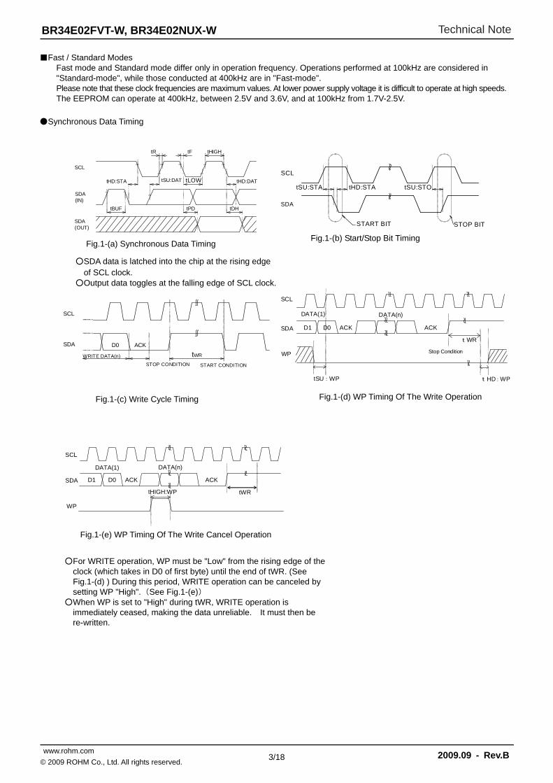
WP effective timing WP is normally fixed at "H" or "L". However, in case WP needs to be controlled in order to cancel the Write command, pay attention to “WP effective timing” as follows: The Write command is canceled by setting WP to "H" within the WP cancellation effective period. The period from the START condition to the rising edge of the clock (which takes in the data DO - the first byte of the Page Write data) is the ‘invalid cancellation period’. WP input is considered inconsequential during this period. The setup time for the rising edge of the SCL, which takes in DO, must be more than 100ns. The period from the rising edge of SCL (which takes in the data D0) to the end of internal write cycle (tWR) is the ‘effective cancellation period’. When WP is set to "H" during tWR, Write operation is stopped, making it necessary to rewrite the data. It is not necessary to wait for tWR (5ms max.) after stopping the Write command by WP because the device is in standby mode.
Command cancellation from the START and STOP conditions
Command input is canceled by successive inputs of START and STOP conditions. (Refer to Fig.42) However, during ACK or data output, the device may set the SDA line to Low, making operation of the START and STOP conditions impossible, and thus preventing reset. In this case execute reset by software. (Refer to Fig.39) The internal address counter will not be determined when operating the Cancel command by the START and STOP conditions during Random, Sequential or Current Read. Operate a Random Read in this case.
・The rising edge of the clock which take in D0
SCL
D0 ACK
AN ENLARGEMENT
SCL
SDA ACK D0
SDA
WP
WP cancellation
invalid period
Data is not
guaranteed No data will be written
Stop of the write
operation
Fig.41 WP effective timing
SLAVE
ADDRESS D7 D6 D5 D4 D3 D2 D1 D0 DATA
tWR
SDA D1
S T A R T
A C K L
A C K L
A C K L
A C K L
S T O P
WORD
ADDRESS
Fig.42 Command cancellation by the START and STOP conditions during input of the Slave Address
SCL
SDA 1 1 0 0
START CONDITION
STOP CONDITION

BR34E02FVT-W, BR34E02NUX-W Technical Note
www.rohm.com 2009.09 - Rev.B© 2009 ROHM Co., Ltd. All rights reserved.
13/18
Microcontroller
THE CAPACITANCE OF BUS LINE (CBUS)COMPUTER
Fig.43 I/O Circuit
I/O Circuit SDA Pin Pull-up Resistor
A pull-up resistor is required because SDA is an NMOS open drain. Determine the resistor value of (RPU) by considering the VIL and IL, and VOL-IOL characteristics. If a large RPU is chosen, the clock frequency needs to be slow. A smaller RPU will result in a larger operating current.
Maximum RPU The maximum of RPU can be determined by the following factors. ①The SDA rise time determined by RPU and the capacitance of the BUS line(CBUS) must be less than tR.
In addition, all other timings must be kept within the AC specifications. ②When the SDA BUS is High, the voltage A at the SDA BUS is determined from the total input leakage(IL) of all
devices connected to the BUS. RPU must be higher than the input High level of the microcontroller and the device, including a noise margin 0.2VCC.
VCC-ILRPU-0.2 VCC ≧ VIH
∴ RPU ≦
0.8VCC-VIHIL
Examples: When VCC =3V, IL=10µA, VIH=0.7 VCC
According to ②
RPU ≦ 0.8x3-0.7x3
10x10-6
≦ 300 [kΩ]
Minimum RPU The minimum value of RPU is determined by following factors. ①Meets the condition that VOLMAX=0.4V, IOLMAX=3mA when the output is Low.
②VOLMAX=0.4V must be lower than the input Low level of the microcontroller and the EEPROMincluding the recommended noise margin of 0.1VCC. VOLMAX ≦ VIL-0.1 VCC Examples: VCC=3V, VOL=0.4V, IOL=3mA, the VIL of the controller and the EEPROM is VIL=0.3VCC, According to ①
and VOL=0.4[V] and VIL=0.3×3 =0.9[V]
o that condition ② is met SCL Pin Pull-up Resistor
When SCL is controlled by the CMOS output the pull-up resistor at SCL is not required. However, should SCL be set to Hi-Z, connection of a pull-up resistor between SCL and VCC is recommended. Several kΩ are recommended for the pull-up resistor in order to drive the output port of the microcontroller.
A0, A1, A2, WP Pin connections
Device Address Pin (A0, A1, A2) connections The status of the device address pins is compared with the device address sent by the Master. One of the devices that is connected to the identical BUS is selected. Pull up or down these pins or connect them to VCC or GND. Pins that are not used as device address (N.C.Pins) may be High, Low, or Hi-Z.
WP Pin connection The WP input allows or prohibits write operations. When WP is High, only Read is available and Write to all address is prohibited. Both Read and Write are available when WP is Low. In the event that the device is used as a ROM, it is recommended that the WP input be pulled up or connected to VCC. When both READ and WRITE are operated, the WP input must be pulled down or connected to GND or controlled.
≧ 867 [Ω]
RPU ≧3-0.43×10 -3
RPU A
BR34E02
SDA PIN
IL IL
∴
VCC-VOL
RPU≦ IOL
RPU ≧VCC-VOL
IOL

BR34E02FVT-W, BR34E02NUX-W Technical Note
www.rohm.com 2009.09 - Rev.B© 2009 ROHM Co., Ltd. All rights reserved.
14/18
Fig.45 Input/Output Collision Timing
VccRS
VccI
≧
≦ I
RS ≧
300[Ω]
∴
RS ≧3
10×10-3
Examples: When VCC=3V, I=10mA
CONTROLLER EEPROM
"L" OUTPUTRS
RPU
"H" OUTPUTMAXIMUMCURRENT
Microcontroller connection Concerning Rs
The open drain interface is recommended for the SDA port in the I2C BUS. However, if the Tri-state CMOS interface is applied to SDA, insert a series resistor (Rs) between the SDA pin of the device and the pull up resistor RPU is recommended, since it will serve to limit the current between the PMOS of the microcontroller, and the NMOS of the EEPROM. Rs also protects the SDA pin from surges. Therefore, Rs is able to be used though open drain inout of the SDA port.
Rs Maximum
The maximum value of Rs is determined by following factors. ①SDA rise time determined by RPU and the capacitance value of the BUS line (CBUS) of SDA must be less than tR. In
addition, the other timings must be within the timing conditions of the AC. ②When the output from SDA is Low, the voltage of the BUS at A is determined by RPU, and Rs must be lower than the
input Low level of the microcontroller, including recommended noise margin (0.1VCC).
Rs Minimum
The minimum value of Rs is determined by the current overload during BUS conflict. Current overload may cause noises in the power line and instantaneous power down. The following conditions must be met, where “I” is the maximum permissible current, which depends on the Vcc line impedance as well as other factors. “I” current must be less than 10mA for EEPROM.
≦
According to ② RS
Examples : When VCC=3V VIL=0.3VCC VOL=0.4V RPU=20kΩ
20×103
1.67[kΩ]
RPU+RS
≦ ×
VIL-VOL-0.1VCC
1.1VCC-VIL
1.1×3-0.3×3
×
0.3×3-0.4-0.1×3
RPU∴
VOL+0.1VCC≦VIL(VCC-VOL)×RS
+
RS ≦
RPU
CONTROLLER
RS
EEPROM
IOL
A
BUS CAPACITANCE
VOL
VCC
VIL
Fig.46 I/O Circuit
ACK
“L” OUTPUT OF EEPROM
'H'OUTPUT OF
CONTROLLER
The “H” output of controller and the “L” output of EEPROM may cause current overload to SDA line.
SCL
SDA
RPU
CONTROLLER
RS
EEPROM
Fig.44 I/O Circuit
Fig.47 I/O Circuit

BR34E02FVT-W, BR34E02NUX-W Technical Note
www.rohm.com 2009.09 - Rev.B© 2009 ROHM Co., Ltd. All rights reserved.
15/18
I2C BUS Input / Output equivalent circuits
Input (A0,A2,SCL)
Input / Output (SDA)
Input (A1)
Input (WP)
Fig.48 Input Pin Circuit
Fig.50 Input Pin Circuit
Fig.49 Input / Output Pin Circuit
Fig.51 Input Pin Circuit

BR34E02FVT-W, BR34E02NUX-W Technical Note
www.rohm.com 2009.09 - Rev.B© 2009 ROHM Co., Ltd. All rights reserved.
16/18
Power Supply Notes VCC increases through the low voltage region where the internal circuit of IC and the microcontroller are unstable. In order to prevent malfunction, the IC has P.O.R and LVCC functionality. During power up, ensure that the following conditions are met to guaranty P.O.R. and LVCC operability.
1. "SDA='H'" and "SCL='L' or 'H'". 2. Follow the recommended conditions of tR, tOFF, Vbot so that P.O.R. will be activated during power up.
tOFF
tR
Vbot
0 Fig.52 VCC rising wavefrom
VCC
3. Prevent SDA and SCL from being "Hi-Z". In case that condition 1. and/or 2. cannot be met, take following actions.
A) If unable to keep Condition 1 (SDA is "Low" during power up) →Make sure that SDA and SCL are "High" as in the figure below.
tLOW
tSU:DAT tDH After Vcc becomes stable
SCL
VCC
SDA
Fig.53 SCL="H" and SDA="L"
tSU:DAT
After Vcc becomes stable
Fig.54 SCL="L" and SDA="L"
B) If unable to keep Condition 2 →After the power stabilizes, execute software reset. (See page 9,10) C) If unable to keep either Condition 1 or 2 →Follow Instruction A first, then B
LVCC Circuit
The LVCC circuit prevents Write operation at low voltage and prevents inadvertent writing. A voltage below the LVCC voltage (1.2V typ.) prohibits Write operation.
VCC Noise Bypass Capacitor
Noise and surges on the power line may cause abnormal function. It is recommended that bypass capacitors (0.1µF) be attached between VCC and GND externally.
Recommended conditions of tR, tOFF, Vbot
tR tOFF Vbot
Below 10ms Above 10ms Below 0.3V
Below 100ms Above 10ms Below 0.2V

BR34E02FVT-W, BR34E02NUX-W Technical Note
www.rohm.com 2009.09 - Rev.B© 2009 ROHM Co., Ltd. All rights reserved.
17/18
Notes for Use 1) Descrived numeric values and data are design representative values, and the values are not guaranteed.
2) We believe that application circuit examples are recommendable, however, in actual use, confirm characteristics further
sufficiently. In the case of use by changing the fixed number of external parts, make your decision with sufficient margin in consideration of static characteristics and transition characteristics and fluctuations of external parts and our LSI.
3) Absolute maximum ratings If the absolute maximum ratings such as impressed voltage and action temperature range and so forth are exceeded, LSI may be destructed. Do not impress voltage and temperature exceeding the absolute maximum ratings. In the case of fear exceeding the absolute maximum ratings, take physical safety countermeasures such as fuses, and see to it that conditions exceeding the absolute maximum ratings should not be impressed to LSI.
4) GND electric potential Set the voltage of GND terminal lowest at any action condition. Make sure that each terminal voltage is lower than that of GND terminal.
5) Heat design In consideration of permissible dissipation in actual use condition, carry out heat design with sufficient margin.
6) Terminal to terminal short circuit and wrong packaging When to package LSI on to a board, pay sufficient attention to LSI direction and displacement. Wrong packaging may destruct LSI. And in the case of short circuit between LSI terminals and terminals and power source, terminal and GND owing to foreign matter, LSI may be destructed.
7) Use in a strong electromagnetic field may cause malfunction, therfore, evaluate design sufficiently.

BR34E02FVT-W, BR34E02NUX-W Technical Note
www.rohm.com 2009.09 - Rev.B© 2009 ROHM Co., Ltd. All rights reserved.
18/18
Ordering part number
B R 3 4 E 0 2 F V T - W E 2
ROHM type BUS type Priduct type Capacity Packagr W : Double cell
34:I2C 02= 2K FVT:TSSOP-B8 Packaging and forming specification
NUX:VSON008X2030 E2: Embossed tape and reel
(TSSOP-B8)
TR: Embossed tape and reel
(VSON008X2030)
(Unit : mm)
SSOP-B8
0.08 M
1 2 3 4
5678
0.1
+0.06-0.040.22
0.3M
IN
0.65(0.52)
3.0±0.2
0.15±0.1
6.4
±0.3
1.15
±0.1
4.4
±0.2
(MAX 3.35 include BURR)
S
0.1
∗ Order quantity needs to be multiple of the minimum quantity.
<Tape and Reel information>
Embossed carrier tapeTape
Quantity
Direction of feed The direction is the 1pin of product is at the upper left when you hold
reel on the left hand and you pull out the tape on the right hand
2500pcs
E2
( )
Direction of feed
Reel1pin
∗ Order quantity needs to be multiple of the minimum quantity.
<Tape and Reel information>
Embossed carrier tapeTape
Quantity
Direction of feed The direction is the 1pin of product is at the upper right when you hold
reel on the left hand and you pull out the tape on the right hand
4000pcs
TR
( )
Direction of feed
Reel1pin
(Unit : mm)
VSON008X2030
5
1
8
4
1.4±
0.1
0.25
1.5±0.1
0.5
0.3±
0.1
0.25+0.05–0.04
C0.25
0.6M
AX
(0.1
2)
0.02
+0.
03–0
.02
3.0±
0.1
2.0±0.1
1PIN MARK
0.08 S
S

DatasheetDatasheet
Notice - GE Rev.002© 2014 ROHM Co., Ltd. All rights reserved.
Notice Precaution on using ROHM Products
1. Our Products are designed and manufactured for application in ordinary electronic equipments (such as AV equipment, OA equipment, telecommunication equipment, home electronic appliances, amusement equipment, etc.). If you intend to use our Products in devices requiring extremely high reliability (such as medical equipment (Note 1), transport equipment, traffic equipment, aircraft/spacecraft, nuclear power controllers, fuel controllers, car equipment including car accessories, safety devices, etc.) and whose malfunction or failure may cause loss of human life, bodily injury or serious damage to property (“Specific Applications”), please consult with the ROHM sales representative in advance. Unless otherwise agreed in writing by ROHM in advance, ROHM shall not be in any way responsible or liable for any damages, expenses or losses incurred by you or third parties arising from the use of any ROHM’s Products for Specific Applications.
(Note1) Medical Equipment Classification of the Specific Applications JAPAN USA EU CHINA
CLASSⅢ CLASSⅢ
CLASSⅡb CLASSⅢ
CLASSⅣ CLASSⅢ
2. ROHM designs and manufactures its Products subject to strict quality control system. However, semiconductor
products can fail or malfunction at a certain rate. Please be sure to implement, at your own responsibilities, adequate safety measures including but not limited to fail-safe design against the physical injury, damage to any property, which a failure or malfunction of our Products may cause. The following are examples of safety measures:
[a] Installation of protection circuits or other protective devices to improve system safety [b] Installation of redundant circuits to reduce the impact of single or multiple circuit failure
3. Our Products are designed and manufactured for use under standard conditions and not under any special or extraordinary environments or conditions, as exemplified below. Accordingly, ROHM shall not be in any way responsible or liable for any damages, expenses or losses arising from the use of any ROHM’s Products under any special or extraordinary environments or conditions. If you intend to use our Products under any special or extraordinary environments or conditions (as exemplified below), your independent verification and confirmation of product performance, reliability, etc, prior to use, must be necessary:
[a] Use of our Products in any types of liquid, including water, oils, chemicals, and organic solvents [b] Use of our Products outdoors or in places where the Products are exposed to direct sunlight or dust [c] Use of our Products in places where the Products are exposed to sea wind or corrosive gases, including Cl2,
H2S, NH3, SO2, and NO2
[d] Use of our Products in places where the Products are exposed to static electricity or electromagnetic waves [e] Use of our Products in proximity to heat-producing components, plastic cords, or other flammable items [f] Sealing or coating our Products with resin or other coating materials [g] Use of our Products without cleaning residue of flux (even if you use no-clean type fluxes, cleaning residue of
flux is recommended); or Washing our Products by using water or water-soluble cleaning agents for cleaning residue after soldering
[h] Use of the Products in places subject to dew condensation
4. The Products are not subject to radiation-proof design. 5. Please verify and confirm characteristics of the final or mounted products in using the Products. 6. In particular, if a transient load (a large amount of load applied in a short period of time, such as pulse. is applied,
confirmation of performance characteristics after on-board mounting is strongly recommended. Avoid applying power exceeding normal rated power; exceeding the power rating under steady-state loading condition may negatively affect product performance and reliability.
7. De-rate Power Dissipation (Pd) depending on Ambient temperature (Ta). When used in sealed area, confirm the actual
ambient temperature. 8. Confirm that operation temperature is within the specified range described in the product specification. 9. ROHM shall not be in any way responsible or liable for failure induced under deviant condition from what is defined in
this document.
Precaution for Mounting / Circuit board design 1. When a highly active halogenous (chlorine, bromine, etc.) flux is used, the residue of flux may negatively affect product
performance and reliability. 2. In principle, the reflow soldering method must be used; if flow soldering method is preferred, please consult with the
ROHM representative in advance. For details, please refer to ROHM Mounting specification

DatasheetDatasheet
Notice - GE Rev.002© 2014 ROHM Co., Ltd. All rights reserved.
Precautions Regarding Application Examples and External Circuits 1. If change is made to the constant of an external circuit, please allow a sufficient margin considering variations of the
characteristics of the Products and external components, including transient characteristics, as well as static characteristics.
2. You agree that application notes, reference designs, and associated data and information contained in this document
are presented only as guidance for Products use. Therefore, in case you use such information, you are solely responsible for it and you must exercise your own independent verification and judgment in the use of such information contained in this document. ROHM shall not be in any way responsible or liable for any damages, expenses or losses incurred by you or third parties arising from the use of such information.
Precaution for Electrostatic
This Product is electrostatic sensitive product, which may be damaged due to electrostatic discharge. Please take proper caution in your manufacturing process and storage so that voltage exceeding the Products maximum rating will not be applied to Products. Please take special care under dry condition (e.g. Grounding of human body / equipment / solder iron, isolation from charged objects, setting of Ionizer, friction prevention and temperature / humidity control).
Precaution for Storage / Transportation 1. Product performance and soldered connections may deteriorate if the Products are stored in the places where:
[a] the Products are exposed to sea winds or corrosive gases, including Cl2, H2S, NH3, SO2, and NO2 [b] the temperature or humidity exceeds those recommended by ROHM [c] the Products are exposed to direct sunshine or condensation [d] the Products are exposed to high Electrostatic
2. Even under ROHM recommended storage condition, solderability of products out of recommended storage time period may be degraded. It is strongly recommended to confirm solderability before using Products of which storage time is exceeding the recommended storage time period.
3. Store / transport cartons in the correct direction, which is indicated on a carton with a symbol. Otherwise bent leads
may occur due to excessive stress applied when dropping of a carton. 4. Use Products within the specified time after opening a humidity barrier bag. Baking is required before using Products of
which storage time is exceeding the recommended storage time period.
Precaution for Product Label QR code printed on ROHM Products label is for ROHM’s internal use only.
Precaution for Disposition When disposing Products please dispose them properly using an authorized industry waste company.
Precaution for Foreign Exchange and Foreign Trade act Since our Products might fall under controlled goods prescribed by the applicable foreign exchange and foreign trade act, please consult with ROHM representative in case of export.
Precaution Regarding Intellectual Property Rights 1. All information and data including but not limited to application example contained in this document is for reference
only. ROHM does not warrant that foregoing information or data will not infringe any intellectual property rights or any other rights of any third party regarding such information or data. ROHM shall not be in any way responsible or liable for infringement of any intellectual property rights or other damages arising from use of such information or data.:
2. No license, expressly or implied, is granted hereby under any intellectual property rights or other rights of ROHM or any
third parties with respect to the information contained in this document.
Other Precaution 1. This document may not be reprinted or reproduced, in whole or in part, without prior written consent of ROHM. 2. The Products may not be disassembled, converted, modified, reproduced or otherwise changed without prior written
consent of ROHM. 3. In no event shall you use in any way whatsoever the Products and the related technical information contained in the
Products or this document for any military purposes, including but not limited to, the development of mass-destruction weapons.
4. The proper names of companies or products described in this document are trademarks or registered trademarks of
ROHM, its affiliated companies or third parties.

DatasheetDatasheet
Notice – WE Rev.001© 2014 ROHM Co., Ltd. All rights reserved.
General Precaution 1. Before you use our Pro ducts, you are requested to care fully read this document and fully understand its contents.
ROHM shall n ot be in an y way responsible or liabl e for fa ilure, malfunction or acci dent arising from the use of a ny ROHM’s Products against warning, caution or note contained in this document.
2. All information contained in this docume nt is current as of the issuing date and subj ect to change without any prior
notice. Before purchasing or using ROHM’s Products, please confirm the la test information with a ROHM sale s representative.
3. The information contained in this doc ument is provi ded on an “as is” basis and ROHM does not warrant that all
information contained in this document is accurate an d/or error-free. ROHM shall not be in an y way responsible or liable for any damages, expenses or losses incurred by you or third parties resulting from inaccuracy or errors of or concerning such information.


![Tudo o que você precisa saber sobre memórias DDR, DDR2 ... · 4/12/2016 Tudo o que você precisa saber sobre memórias DDR, DDR2, DDR3 e DDR4 [página para impressão] - Clube do](https://img.dokumen.tips/doc/110x75/5c20f52909d3f24d208c518c/tudo-o-que-voce-precisa-saber-sobre-memorias-ddr-ddr2-4122016-tudo.jpg)