Embed Size (px)
Citation preview
Datasheet
〇Product structure : Silicon monolithic integrated circuit 〇This product has no designed protection against radioactive rays
.
1/19
TSZ02201-0242AAJ00030-1-2
© 2014 ROHM Co., Ltd. All rights reserved. 29.Aug.2014 Rev. 002 TSZ22111 • 15 • 001
www.rohm.com
UCSP50L1C
1.80mm x 1.50mm x 0.57mm
STBYP
STBYN
VIN
LX
VOUTP
VREG
V+
5.4V/max50mA
VOUTNV-
-5.4V/max50mA
CP1
CP2
VIN
2.5V to 4.5V C1
4.7µF
LLX
4.7µH
CVOP
4.7µF
CVON
4.7µF
CVREG
4.7µF
CCP
2.2µF
PGND1
AGND
PGND2
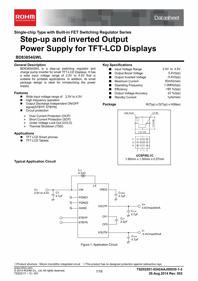
Single-chip Type with Built-in FET Switching Regulator Series
Step-up and inverted Output Power Supply for TFT-LCD Displays
BD83854GWL
General Description BD83854GWL is a step-up switching regulator and charge pump inverter for small TFT-LCD Displays. It has a wide input voltage range of 2.5V to 4.5V that is suitable for portable applications. In addition, its small package design is ideal for miniaturizing the power supply.
Features
Wide input voltage range of 2.5V to 4.5V High frequency operation Output Discharge Independent ON/OFF
signal(STBYP, STBYN) Circuit protection
Over Current Protection (OCP) Short Current Protection (SCP) Under Voltage Lock Out (UVLO) Thermal Shutdown (TSD)
Applications TFT LCD Smart phones TFT LCD Tablets
Key Specifications
■ Input Voltage Range
■ Output Boost Voltage
■ Output Inverted Voltage
■ Maximum Current
■ Operating Frequency
■ Efficiency
■ Output Voltage Accuracy
■ Standby Current
2.5V to 4.5V
5.4V(typ)
-5.4V(typ)
50mA(max)
1.0MHz(typ)
>85 %(typ)
±2 %(typ)
1µA(max)
Package W(Typ) x D(Typ) x H(Max)
Typical Application Circuit
Figure 1. Application Circuit
2/19
TSZ02201-0242AAJ00030-1-2
© 2014 ROHM Co., Ltd. All rights reserved. 29.Aug.2014 Rev. 002
www.rohm.com
TSZ22111 • 15 • 001
BD83854GWL
Contents
General Description .................................................................................................................................................... 1
Features ....................................................................................................................................................................... 1
Applications ................................................................................................................................................................ 1
Key Specifications ...................................................................................................................................................... 1
Package W(Typ) x D(Typ) x H(Max) ....................................................................................................................... 1
Typical Application Circuit ......................................................................................................................................... 1
Pin Configuration ........................................................................................................................................................ 3
Pin Description............................................................................................................................................................ 3
Block Diagram ............................................................................................................................................................. 4
Absolute Maximum Ratings (Ta = 25°C) ................................................................................................................... 4
Recommended Operating Conditions ...................................................................................................................... 4
Electrical Characteristics (Unless otherwise specified VIN=3.7V Ta=25°C) .......................................................... 5
Typical Performance Curves ..................................................................................................................................... 6
Application Information ........................................................................................................................................... 11
Description of Protection Circuits ....................................................................................................................... 11
Application Example ............................................................................................................................................. 13
Selection of External Components ...................................................................................................................... 13
Power Dissipation ..................................................................................................................................................... 14
I/O Equivalent Circuit ............................................................................................................................................... 15
Operational Notes ..................................................................................................................................................... 16
Ordering Information ................................................................................................................................................ 18
Physical Dimension, Tape and Reel Information ................................................................................................... 18
Revision History ....................................................................................................................................................... 19
3/19
TSZ02201-0242AAJ00030-1-2
© 2014 ROHM Co., Ltd. All rights reserved. 29.Aug.2014 Rev. 002
www.rohm.com
TSZ22111 • 15 • 001
BD83854GWL
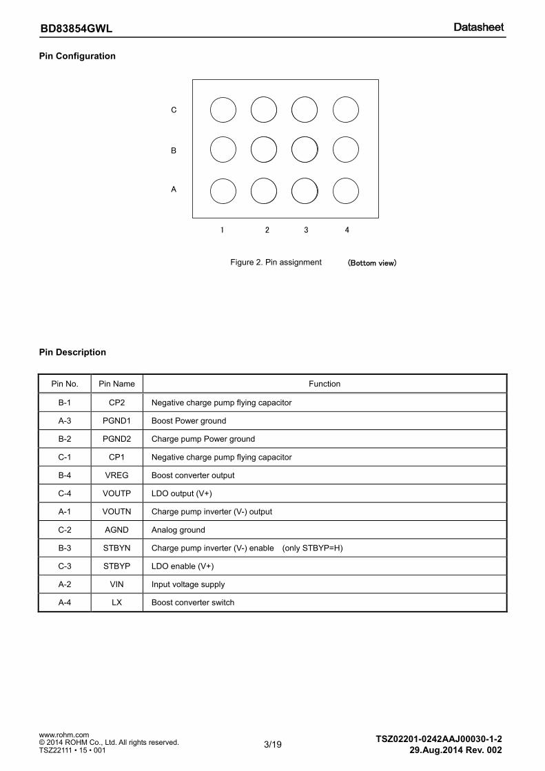
Figure 2. Pin assignment
Pin Configuration
Pin Description
Pin No. Pin Name Function
B-1 CP2 Negative charge pump flying capacitor
A-3 PGND1 Boost Power ground
B-2 PGND2 Charge pump Power ground
C-1 CP1 Negative charge pump flying capacitor
B-4 VREG Boost converter output
C-4 VOUTP LDO output (V+)
A-1 VOUTN Charge pump inverter (V-) output
C-2 AGND Analog ground
B-3 STBYN Charge pump inverter (V-) enable (only STBYP=H)
C-3 STBYP LDO enable (V+)
A-2 VIN Input voltage supply
A-4 LX Boost converter switch
(Bottom view)
A
B
C
1 2 3 4
4/19
TSZ02201-0242AAJ00030-1-2
© 2014 ROHM Co., Ltd. All rights reserved. 29.Aug.2014 Rev. 002
www.rohm.com
TSZ22111 • 15 • 001
BD83854GWL
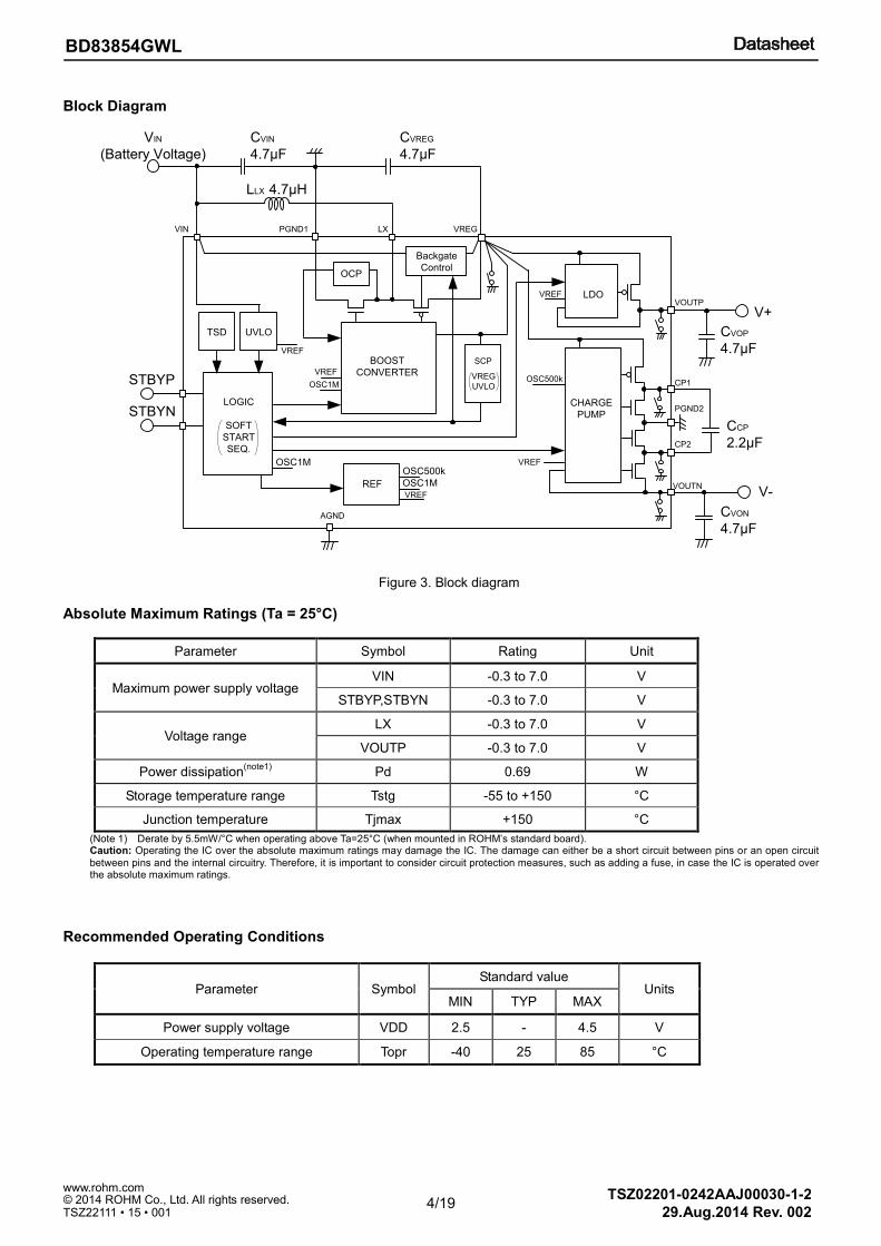
Block Diagram
Absolute Maximum Ratings (Ta = 25°C)
Parameter Symbol Rating Unit
Maximum power supply voltage VIN -0.3 to 7.0 V
STBYP,STBYN -0.3 to 7.0 V
Voltage range LX -0.3 to 7.0 V
VOUTP -0.3 to 7.0 V
Power dissipation(note1)
Pd 0.69 W
Storage temperature range Tstg -55 to +150 °C
Junction temperature Tjmax +150 °C
(Note 1) Derate by 5.5mW/°C when operating above Ta=25°C (when mounted in ROHM’s standard board). Caution: Operating the IC over the absolute maximum ratings may damage the IC. The damage can either be a short circuit between pins or an open circuit
between pins and the internal circuitry. Therefore, it is important to consider circuit protection measures, such as adding a fuse, in case the IC is operated over the absolute maximum ratings.
Recommended Operating Conditions
Parameter Symbol Standard value
Units MIN TYP MAX
Power supply voltage VDD 2.5 - 4.5 V
Operating temperature range Topr -40 25 85 °C
Figure 3. Block diagram
V+
VIN
(Battery Voltage)
BOOST
CONVERTER
CVIN
4.7µF
CVREG
4.7µF
CCP
2.2µF
LLX 4.7µH
LDO
V-
CVON
4.7µF
CVOP
4.7µF
CHARGE
PUMP
VREG
UVLO
LOGIC
SOFT
START
SEQ.
REFVREF
VREF
VREF
VREFOSC500kSTBYP
STBYN
UVLO
OSC1M
Backgate
Control
AGND
VIN PGND1 LX VREG
VOUTP
CP1
PGND2
CP2
VOUTN
TSD
OSC1M
SCP
OCP
OSC500kOSC1M
VREF
5/19
TSZ02201-0242AAJ00030-1-2
© 2014 ROHM Co., Ltd. All rights reserved. 29.Aug.2014 Rev. 002
www.rohm.com
TSZ22111 • 15 • 001
BD83854GWL
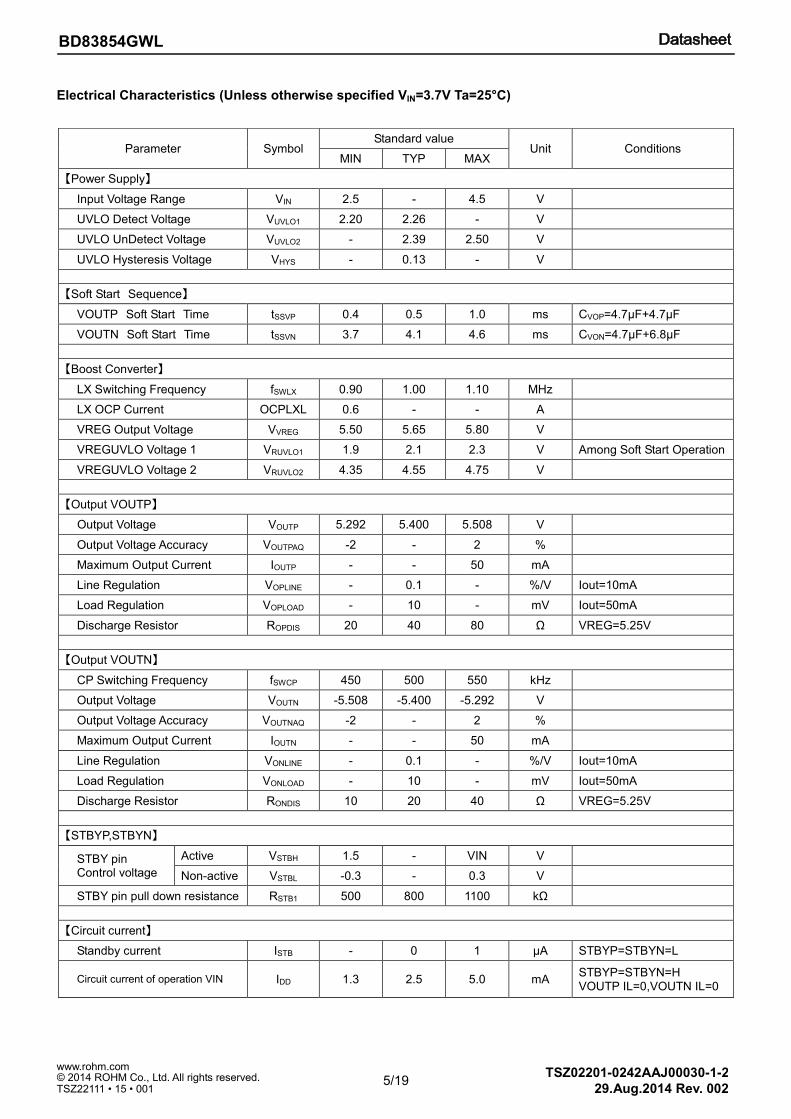
Electrical Characteristics (Unless otherwise specified VIN=3.7V Ta=25°C)
Parameter Symbol Standard value
Unit Conditions MIN TYP MAX
【Power Supply】
Input Voltage Range VIN 2.5 - 4.5 V
UVLO Detect Voltage VUVLO1 2.20 2.26 - V
UVLO UnDetect Voltage VUVLO2 - 2.39 2.50 V
UVLO Hysteresis Voltage VHYS - 0.13 - V
【Soft Start Sequence】
VOUTP Soft Start Time tSSVP 0.4 0.5 1.0 ms CVOP=4.7µF+4.7µF
VOUTN Soft Start Time tSSVN 3.7 4.1 4.6 ms CVON=4.7µF+6.8µF
【Boost Converter】
LX Switching Frequency fSWLX 0.90 1.00 1.10 MHz
LX OCP Current OCPLXL 0.6 - - A
VREG Output Voltage VVREG 5.50 5.65 5.80 V
VREGUVLO Voltage 1 VRUVLO1 1.9 2.1 2.3 V Among Soft Start Operation
VREGUVLO Voltage 2 VRUVLO2 4.35 4.55 4.75 V
【Output VOUTP】
Output Voltage VOUTP 5.292 5.400 5.508 V
Output Voltage Accuracy VOUTPAQ -2 - 2 %
Maximum Output Current IOUTP - - 50 mA
Line Regulation VOPLINE - 0.1 - %/V Iout=10mA
Load Regulation VOPLOAD - 10 - mV Iout=50mA
Discharge Resistor ROPDIS 20 40 80 Ω VREG=5.25V
【Output VOUTN】
CP Switching Frequency fSWCP 450 500 550 kHz
Output Voltage VOUTN -5.508 -5.400 -5.292 V
Output Voltage Accuracy VOUTNAQ -2 - 2 %
Maximum Output Current IOUTN - - 50 mA
Line Regulation VONLINE - 0.1 - %/V Iout=10mA
Load Regulation VONLOAD - 10 - mV Iout=50mA
Discharge Resistor RONDIS 10 20 40 Ω VREG=5.25V
【STBYP,STBYN】
STBY pin Control voltage
Active VSTBH 1.5 - VIN V
Non-active VSTBL -0.3 - 0.3 V
STBY pin pull down resistance RSTB1 500 800 1100 kΩ
【Circuit current】
Standby current ISTB - 0 1 µA STBYP=STBYN=L
Circuit current of operation VIN IDD 1.3 2.5 5.0 mA STBYP=STBYN=H VOUTP IL=0,VOUTN IL=0
6/19
TSZ02201-0242AAJ00030-1-2
© 2014 ROHM Co., Ltd. All rights reserved. 29.Aug.2014 Rev. 002
www.rohm.com
TSZ22111 • 15 • 001
BD83854GWL
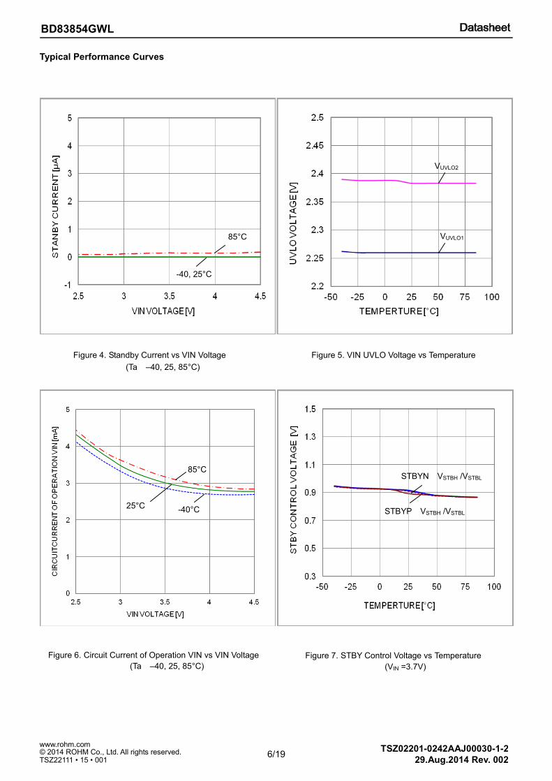
Typical Performance Curves
Figure 4. Standby Current vs VIN Voltage
Figure 6. Circuit Current of Operation VIN vs VIN Voltage
Figure 5. VIN UVLO Voltage vs Temperature
Figure 7. STBY Control Voltage vs Temperature
VUVLO2
VUVLO1
(Ta –40, 25, 85°C)
(Ta –40, 25, 85°C)
-40°C
85°C
85°C
-40, 25°C
STBYP VSTBH /VSTBL
(VIN =3.7V)
STBYN VSTBH /VSTBL
25°C
7/19
TSZ02201-0242AAJ00030-1-2
© 2014 ROHM Co., Ltd. All rights reserved. 29.Aug.2014 Rev. 002
www.rohm.com
TSZ22111 • 15 • 001
BD83854GWL
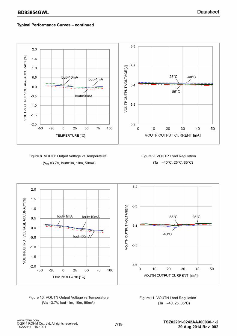
Typical Performance Curves – continued
Figure 8. VOUTP Output Voltage vs Temperature
Figure 10. VOUTN Output Voltage vs Temperature
Figure 9. VOUTP Load Regulation
Figure 11. VOUTN Load Regulation
(Ta –40°C, 25°C, 85°C)
(Ta –40, 25, 85°C) (VIN =3.7V, Iout=1m, 10m, 50mA)
85°C
-40°C
85°C
-40°C
Iout=50mA
Iout=10mA
Iout=1mA
Iout=50mA
(VIN =3.7V, Iout=1m, 10m, 50mA)
25°C Iout=10mA
Iout=1mA 25°C
8/19
TSZ02201-0242AAJ00030-1-2
© 2014 ROHM Co., Ltd. All rights reserved. 29.Aug.2014 Rev. 002
www.rohm.com
TSZ22111 • 15 • 001
BD83854GWL
Typical Performance Curves – continued
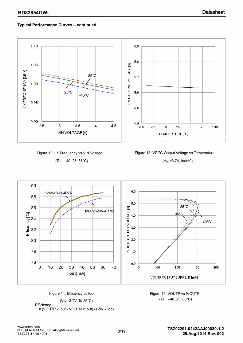
Figure 12. LX Frequency vs VIN Voltage
Figure 14. Efficiency vs Iout
Figure 13. VREG Output Voltage vs Temperature
Figure 15. VOUTP vs IVOUTP
(VIN =3.7V, Ta 25°C) Efficiency
= (VOUTP x Iout - VOUTN x Iout) / (VIN x Idd)
(Ta –40, 25, 85°C) (VIN =3.7V, Iout=0)
(Ta –40, 25, 85°C)
1269AS-H-4R7N
MLP2520V-4R7M 85°C
-40°C
-40°C
85°C
25°C
25°C
9/19
TSZ02201-0242AAJ00030-1-2
© 2014 ROHM Co., Ltd. All rights reserved. 29.Aug.2014 Rev. 002
www.rohm.com
TSZ22111 • 15 • 001
BD83854GWL
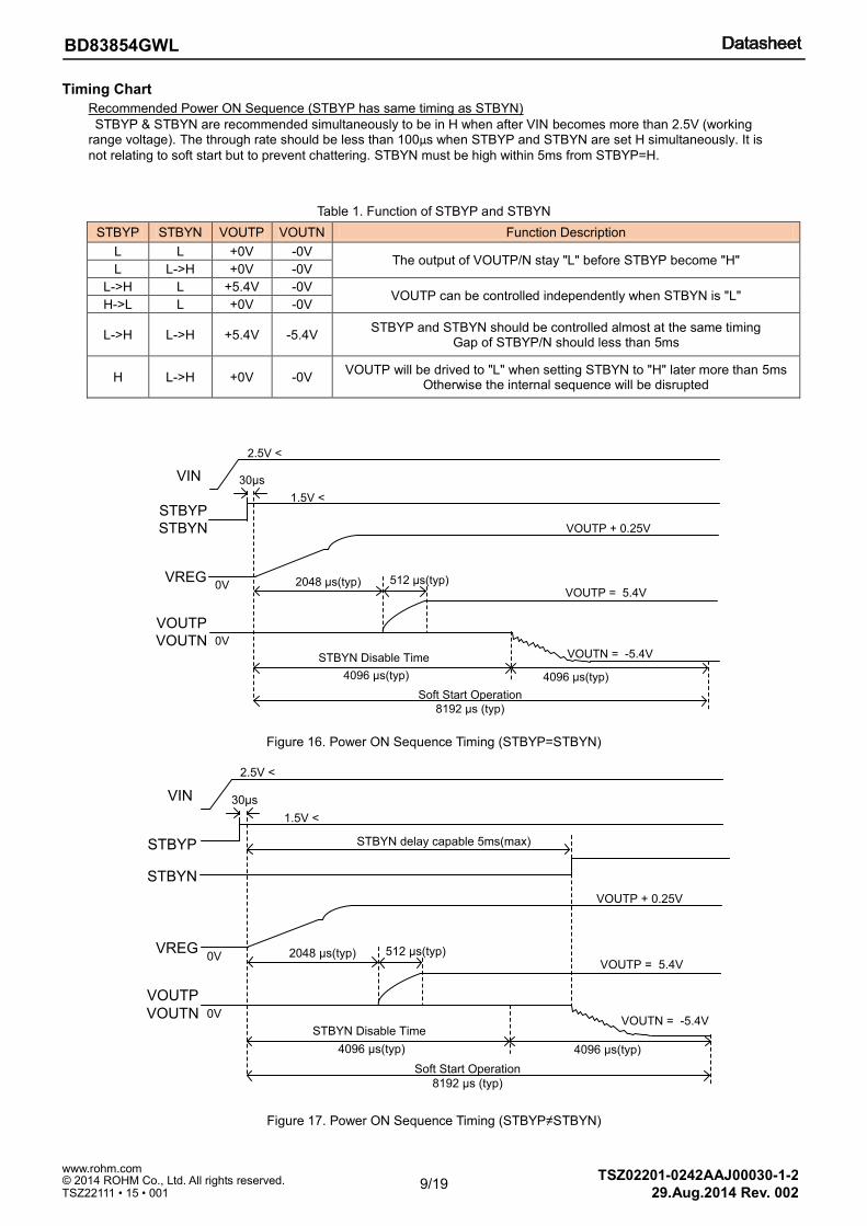
STBYP STBYN VOUTP VOUTN Function Description
L L +0V -0V The output of VOUTP/N stay "L" before STBYP become "H"
L L->H +0V -0V
L->H L +5.4V -0V VOUTP can be controlled independently when STBYN is "L"
H->L L +0V -0V
L->H L->H +5.4V -5.4V STBYP and STBYN should be controlled almost at the same timing
Gap of STBYP/N should less than 5ms
H L->H +0V -0V VOUTP will be drived to "L" when setting STBYN to "H" later more than 5ms
Otherwise the internal sequence will be disrupted
0V
STBYP
VREG
30µs
VOUTP + 0.25V
0V
VOUTP
VOUTN
VOUTP = 5.4V
VOUTN = -5.4V
2048 µs(typ)
Soft Start Operation
8192 µs (typ)
4096 µs(typ)
512 µs(typ)
4096 µs(typ)
STBYN Disable Time
VIN
2.5V <
1.5V <
STBYN
STBYN delay capable 5ms(max)
Timing Chart
Recommended Power ON Sequence (STBYP has same timing as STBYN)
STBYP & STBYN are recommended simultaneously to be in H when after VIN becomes more than 2.5V (working range voltage). The through rate should be less than 100µs when STBYP and STBYN are set H simultaneously. It is
not relating to soft start but to prevent chattering. STBYN must be high within 5ms from STBYP=H.
Table 1. Function of STBYP and STBYN
Figure 16. Power ON Sequence Timing (STBYP=STBYN)
Figure 17. Power ON Sequence Timing (STBYP≠STBYN)
0V
STBYP
STBYN
VREG
30µs
VOUTP + 0.25V
0V
VOUTP
VOUTN
VOUTP = 5.4V
VOUTN = -5.4V
2048 µs(typ)
Soft Start Operation
8192 µs (typ)
4096 µs(typ)
512 µs(typ)
4096 µs(typ)
STBYN Disable Time
VIN
2.5V <
1.5V <
10/19
TSZ02201-0242AAJ00030-1-2
© 2014 ROHM Co., Ltd. All rights reserved. 29.Aug.2014 Rev. 002
www.rohm.com
TSZ22111 • 15 • 001
BD83854GWL
0V
30µs
STBYP
STBYN
VREG
VOUTP
VOUTN
90% down 216µs
90% down 356µs(typ)
90% down 4.0ms(typ)
Shutdown Time
4.0ms (typ)
+5.4V
-5.4V
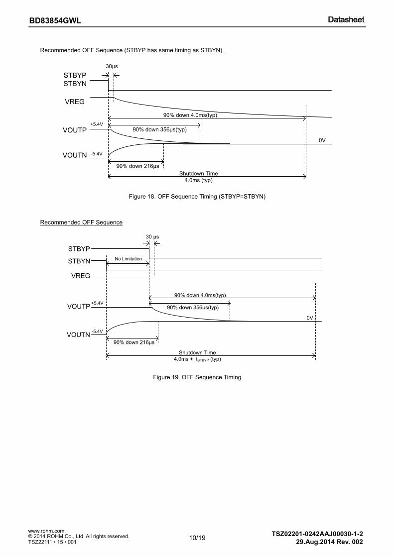
Recommended OFF Sequence (STBYP has same timing as STBYN)
Figure 18. OFF Sequence Timing (STBYP=STBYN)
Recommended OFF Sequence
Figure 19. OFF Sequence Timing
90% down 216µs
90% down 356µs(typ)
0V
30 µs
STBYP
VREG
VOUTP
STBYN
VOUTN
90% down 4.0ms(typ)
Shutdown Time
4.0ms + tSTBYP (typ)
No Limitation
+5.4V
-5.4V
11/19
TSZ02201-0242AAJ00030-1-2
© 2014 ROHM Co., Ltd. All rights reserved. 29.Aug.2014 Rev. 002
www.rohm.com
TSZ22111 • 15 • 001
BD83854GWL
VIN
VREG
VOUTP
VOUTN
2.2V
35µs
2.4V
2ms 2ms
35µs
normal operation
mode
normal operation
mode
UVLO
Detect
UVLO
UnDetect
SCP detect level
STBYP
STBYN
VOUTN
SCP ON
VOUTP
VREG
VREG monitor 2.1V(typ)
SCP function
ON
1.5ms
(typ) 8.2ms(typ)
Soft Start Operation
VREG monitor 4.55V (typ)
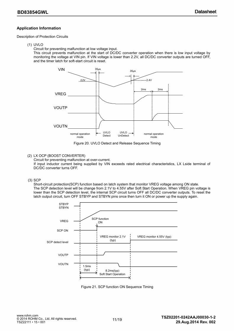
Application Information Description of Protection Circuits
(1) UVLO
Circuit for preventing malfunction at low voltage input. This circuit prevents malfunction at the start of DC/DC converter operation when there is low input voltage by monitoring the voltage at VIN pin. If VIN voltage is lower than 2.2V, all DC/DC converter outputs are turned OFF, and the timer latch for soft-start circuit is reset.
Figure 20. UVLO Detect and Release Sequence Timing
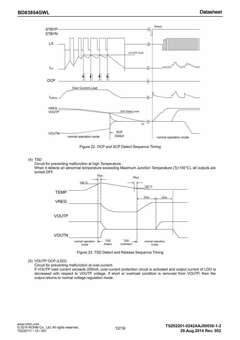
(2) LX OCP (BOOST CONVERTER)
Circuit for preventing malfunction at over-current. If input inductor current being supplied by VIN exceeds rated electrical characteristics, LX Lside terminal of DC/DC converter turns OFF.
(3) SCP Short-circuit protection(SCP) function based on latch system that monitor VREG voltage among ON state. The SCP detection level will be change from 2.1V to 4.55V after Soft Start Operation. When VREG pin voltage is lower than the SCP detection level, the internal SCP circuit turns OFF all DC/DC converter outputs. To reset the latch output circuit, turn OFF STBYP and STBYN pins once then turn it ON or power up the supply again.
Figure 21. SCP function ON Sequence Timing
12/19
TSZ02201-0242AAJ00030-1-2
© 2014 ROHM Co., Ltd. All rights reserved. 29.Aug.2014 Rev. 002
www.rohm.com
TSZ22111 • 15 • 001
BD83854GWL
LX
ILX
OCP
IVREG
VREG
VOUTP
VOUTN
0V
SCP Detect Level
Over Current Load
SCP
Detectnormal operation mode
STBYP
STBYN
Restart
LX OCP Level
normal operation mode
TEMP
VREG
VOUTP
VOUTN
150 ℃
10µs
2ms 2ms
30µs
125 ℃
normal operation
mode
normal operation
mode
TSD
Detect
TSD
UnDetect
Figure 22. OCP and SCP Detect Sequence Timing
(4) TSD
Circuit for preventing malfunction at high Temperature. When it detects an abnormal temperature exceeding Maximum Junction Temperature (Tj=150°C), all outputs are turned OFF.
Figure 23. TSD Detect and Release Sequence Timing
(5) VOUTP OCP (LDO)
Circuit for preventing malfunction at over-current. If VOUTP load current exceeds 200mA, over-current protection circuit is activated and output current of LDO is decreased with respect to VOUTP voltage. If short or overload condition is removed from VOUTP, then the output returns to normal voltage regulation mode.
13/19
TSZ02201-0242AAJ00030-1-2
© 2014 ROHM Co., Ltd. All rights reserved. 29.Aug.2014 Rev. 002
www.rohm.com
TSZ22111 • 15 • 001
BD83854GWL
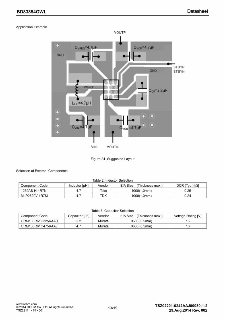
Application Example
Figure 24. Suggested Layout
Selection of External Components
Table 2. Inductor Selection
Component Code Inductor [µH] Vendor EIA Size (Thickness max.) DCR (Typ.) [Ω]
1269AS-H-4R7N 4.7 Toko 1008(1.0mm) 0.25
MLP2520V-4R7M 4.7 TDK 1008(1.0mm) 0.24
Table 3. Capacitor Selection
Component Code Capacitor [µF] Vendor EIA Size (Thickness max.) Voltage Rating [V]
GRM188R61C225KAAD 2.2 Murata 0603 (0.9mm) 16
GRM188R61C475KAAJ 4.7 Murata 0603 (0.9mm) 16
14/19
TSZ02201-0242AAJ00030-1-2
© 2014 ROHM Co., Ltd. All rights reserved. 29.Aug.2014 Rev. 002
www.rohm.com
TSZ22111 • 15 • 001
BD83854GWL
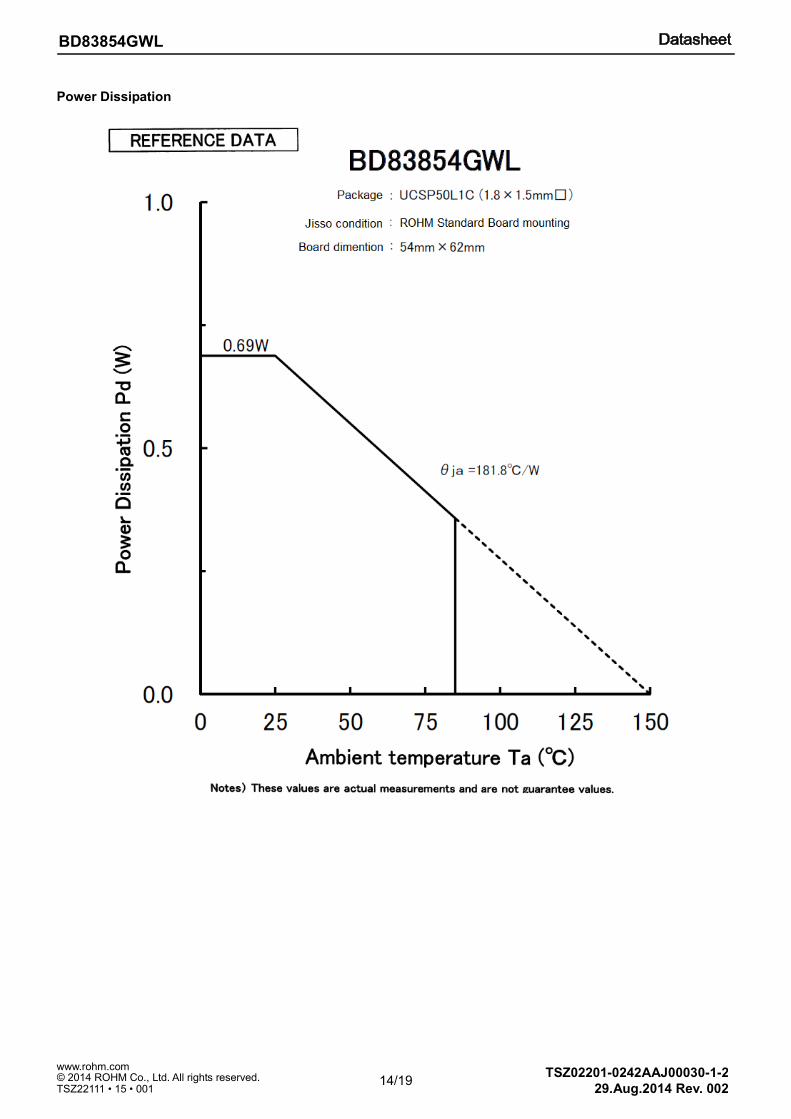
Power Dissipation
15/19
TSZ02201-0242AAJ00030-1-2
© 2014 ROHM Co., Ltd. All rights reserved. 29.Aug.2014 Rev. 002
www.rohm.com
TSZ22111 • 15 • 001
BD83854GWL
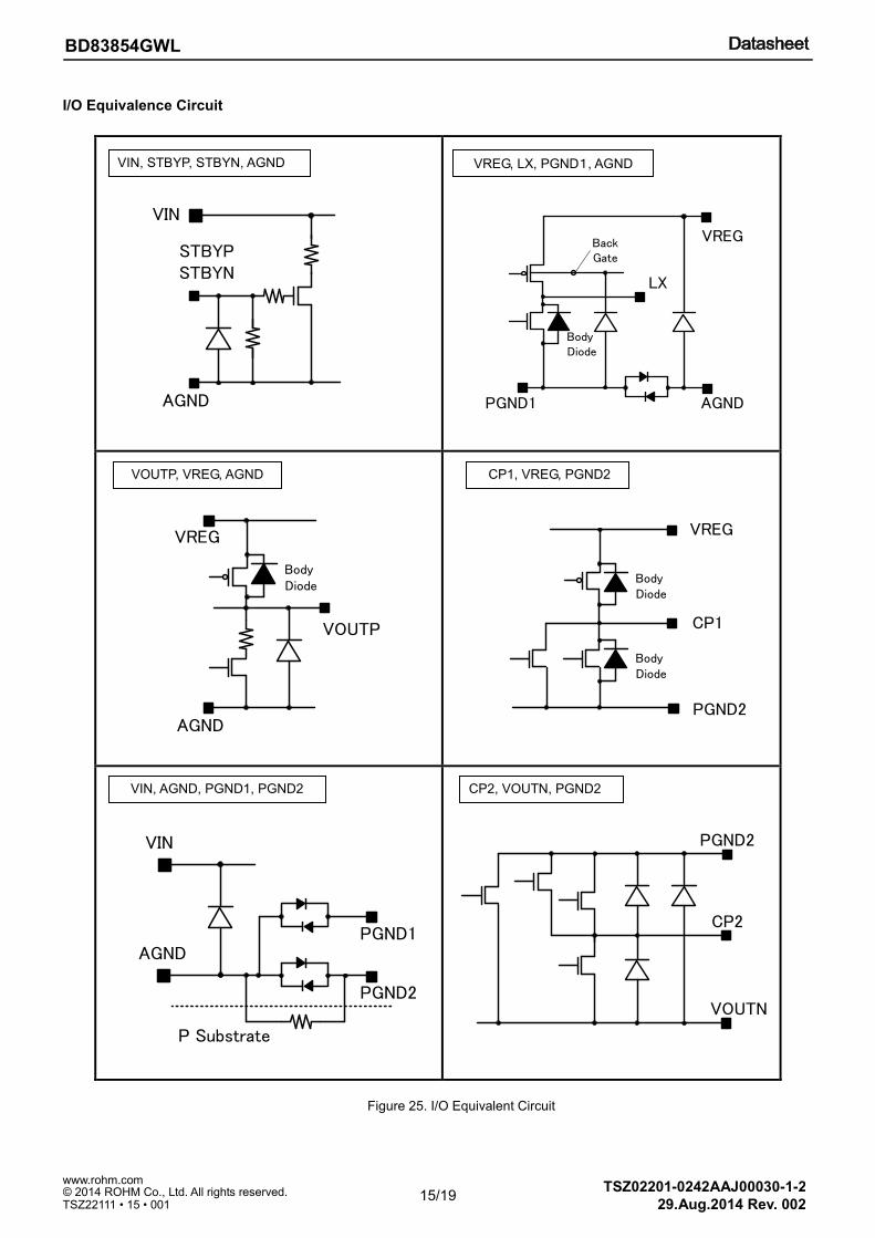
I/O Equivalence Circuit
Figure 25. I/O Equivalent Circuit
VIN, STBYP, STBYN, AGND VREG, LX, PGND1, AGND
VOUTP, VREG, AGND CP1, VREG, PGND2
VIN, AGND, PGND1, PGND2
CP2, VOUTN, PGND2
VREGBackGate
LX
Body Diode
AGNDPGND1
STBYPSTBYN
VIN
AGND
Body Diode
VOUTP
AGND
VREG
Body Diode
Body Diode
CP1
PGND2
VREG
PGND2
VOUTN
CP2
VIN
AGND
PGND2
PGND1
P Substrate
16/19
TSZ02201-0242AAJ00030-1-2
© 2014 ROHM Co., Ltd. All rights reserved. 29.Aug.2014 Rev. 002
www.rohm.com
TSZ22111 • 15 • 001
BD83854GWL
Operational Notes
1. Reverse Connection of Power Supply
Connecting the power supply in reverse polarity can damage the IC. Take precautions against reverse polarity when connecting the power supply, such as mounting an external diode between the power supply and the IC’s power supply pins.
2. Power Supply Lines
Design the PCB layout pattern to provide low impedance supply lines. Separate the ground and supply lines of the digital and analog blocks to prevent noise in the ground and supply lines of the digital block from affecting the analog block. Furthermore, connect a capacitor to ground at all power supply pins. Consider the effect of temperature and aging on the capacitance value when using electrolytic capacitors.
3. Ground Voltage
Except for pins the output the input of which were designed to go below ground, ensure that no pins are at a voltage below that of the ground pin at any time, even during transient condition.
4. Ground Wiring Pattern
When using both small-signal and large-current ground traces, the two ground traces should be routed separately but connected to a single ground at the reference point of the application board to avoid fluctuations in the small-signal ground caused by large currents. Also ensure that the ground traces of external components do not cause variations on the ground voltage. The ground lines must be as short and thick as possible to reduce line impedance.
5. Thermal Consideration
Should by any chance the power dissipation rating be exceeded the rise in temperature of the chip may result in
deterioration of the properties of the chip. The absolute maximum rating of the Pd stated in this specification is when
the IC is mounted on a 70mm x 70mm x 1.6mm glass epoxy board. In case of exceeding this absolute maximum
rating, increase the board size and copper area to prevent exceeding the Pd rating.
6. Recommended Operating Conditions
These conditions represent a range within which the expected characteristics of the IC can be approximately obtained. The electrical characteristics are guaranteed under the conditions of each parameter.
7. Inrush Current
When power is first supplied to the IC, it is possible that the internal logic may be unstable and inrush current may flow instantaneously due to the internal powering sequence and delays, especially if the IC has more than one power supply. Therefore, give special consideration to power coupling capacitance, power wiring, width of ground wiring, and routing of connections.
8. Operation Under Strong Electromagnetic Field
Operating the IC in the presence of a strong electromagnetic field may cause the IC to malfunction.
9. Testing on Application Boards
When testing the IC on an application board, connecting a capacitor directly to a low-impedance output pin may subject the IC to stress. Always discharge capacitors completely after each process or step. The IC’s power supply should always be turned off completely before connecting or removing it from the test setup during the inspection process. To prevent damage from static discharge, ground the IC during assembly and use similar precautions during transport and storage.
10. Inter-pin Short and Mounting Errors
Ensure that the direction and position are correct when mounting the IC on the PCB. Incorrect mounting may result in damaging the IC. Avoid nearby pins being shorted to each other especially to ground, power supply and output pin. Inter-pin shorts could be due to many reasons such as metal particles, water droplets (in very humid environment) and unintentional solder bridge deposited in between pins during assembly to name a few.
17/19
TSZ02201-0242AAJ00030-1-2
© 2014 ROHM Co., Ltd. All rights reserved. 29.Aug.2014 Rev. 002
www.rohm.com
TSZ22111 • 15 • 001
BD83854GWL
Operational Notes – continued
11. Unused Input Pins
Input pins of an IC are often connected to the gate of a MOS transistor. The gate has extremely high impedance and extremely low capacitance. If left unconnected, the electric field from the outside can easily charge it. The small charge acquired in this way is enough to produce a significant effect on the conduction through the transistor and cause unexpected operation of the IC. So unless otherwise specified, unused input pins should be connected to the power supply or ground line.
12. Regarding the Input Pin of the IC
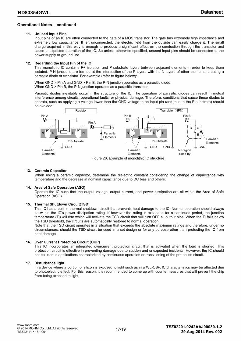
This monolithic IC contains P+ isolation and P substrate layers between adjacent elements in order to keep them isolated. P-N junctions are formed at the intersection of the P layers with the N layers of other elements, creating a parasitic diode or transistor. For example (refer to figure below):
When GND > Pin A and GND > Pin B, the P-N junction operates as a parasitic diode. When GND > Pin B, the P-N junction operates as a parasitic transistor.
Parasitic diodes inevitably occur in the structure of the IC. The operation of parasitic diodes can result in mutual interference among circuits, operational faults, or physical damage. Therefore, conditions that cause these diodes to operate, such as applying a voltage lower than the GND voltage to an input pin (and thus to the P substrate) should be avoided.
Figure 26. Example of monolithic IC structure
13. Ceramic Capacitor
When using a ceramic capacitor, determine the dielectric constant considering the change of capacitance with temperature and the decrease in nominal capacitance due to DC bias and others.
14. Area of Safe Operation (ASO)
Operate the IC such that the output voltage, output current, and power dissipation are all within the Area of Safe Operation (ASO).
15. Thermal Shutdown Circuit(TSD)
This IC has a built-in thermal shutdown circuit that prevents heat damage to the IC. Normal operation should always be within the IC’s power dissipation rating. If however the rating is exceeded for a continued period, the junction temperature (Tj) will rise which will activate the TSD circuit that will turn OFF all output pins. When the Tj falls below the TSD threshold, the circuits are automatically restored to normal operation. Note that the TSD circuit operates in a situation that exceeds the absolute maximum ratings and therefore, under no circumstances, should the TSD circuit be used in a set design or for any purpose other than protecting the IC from heat damage.
16. Over Current Protection Circuit (OCP)
This IC incorporates an integrated overcurrent protection circuit that is activated when the load is shorted. This protection circuit is effective in preventing damage due to sudden and unexpected incidents. However, the IC should not be used in applications characterized by continuous operation or transitioning of the protection circuit.
17. Disturbance light
In a device where a portion of silicon is exposed to light such as in a WL-CSP, IC characteristics may be affected due to photoelectric effect. For this reason, it is recommended to come up with countermeasures that will prevent the chip from being exposed to light.
N NP
+ P
N NP
+
P Substrate
GND
NP
+
N NP
+N P
P Substrate
GND GND
Parasitic
Elements
Pin A
Pin A
Pin B Pin B
B C
E
Parasitic
Elements
GNDParasitic
Elements
CB
E
Transistor (NPN)Resistor
N Region
close-by
Parasitic
Elements
18/19
TSZ02201-0242AAJ00030-1-2
© 2014 ROHM Co., Ltd. All rights reserved. 29.Aug.2014 Rev. 002
www.rohm.com
TSZ22111 • 15 • 001
BD83854GWL
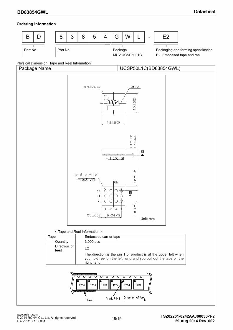
Ordering Information
B D 8 3 8 5 4 G W L - E2
Part No. Part No.
Package
MUV:UCSP50L1C
Packaging and forming specification
E2: Embossed tape and reel
Physical Dimension, Tape and Reel Information
Package Name UCSP50L1C(BD83854GWL)
< Tape and Reel Information >
Tape Embossed carrier tape
Quantity 3,000 pcs
Direction of feed
E2
The direction is the pin 1 of product is at the upper left when you hold reel on the left hand and you pull out the tape on the right hand
3854
Unit: mm
19/19
TSZ02201-0242AAJ00030-1-2
© 2014 ROHM Co., Ltd. All rights reserved. 29.Aug.2014 Rev. 002
www.rohm.com
TSZ22111 • 15 • 001
BD83854GWL
Revision History
Date Revision Changes
4.Jun.2014 001 New Release
29.Aug.2014 002
Page 2/19 Added Contents Page 4/19 Updated Note1 and added Caution Page 17/19 Updated Ground Voltage and added Disturbance light Page 18/19 Updated Physical Dimension Tape and Reel Information
Notice-GE Rev.003 © 2013 ROHM Co., Ltd. All rights reserved.
Notice
Precaution on using ROHM Products 1. Our Products are designed and manufactured for application in ordinary electronic equipments (such as AV equipment,
OA equipment, telecommunication equipment, home electronic appliances, amusement equipment, etc.). If you intend to use our Products in devices requiring extremely high reliability (such as medical equipment
(Note 1), transport
equipment, traffic equipment, aircraft/spacecraft, nuclear power controllers, fuel controllers, car equipment including car accessories, safety devices, etc.) and whose malfunction or failure may cause loss of human life, bodily injury or serious damage to property (“Specific Applications”), please consult with the ROHM sales representative in advance. Unless otherwise agreed in writing by ROHM in advance, ROHM shall not be in any way responsible or liable for any damages, expenses or losses incurred by you or third parties arising from the use of any ROHM’s Products for Specific Applications.
(Note1) Medical Equipment Classification of the Specific Applications
JAPAN USA EU CHINA
CLASSⅢ CLASSⅢ
CLASSⅡb CLASSⅢ
CLASSⅣ CLASSⅢ
2. ROHM designs and manufactures its Products subject to strict quality control system. However, semiconductor
products can fail or malfunction at a certain rate. Please be sure to implement, at your own responsibilities, adequate safety measures including but not limited to fail-safe design against the physical injury, damage to any property, which a failure or malfunction of our Products may cause. The following are examples of safety measures:
[a] Installation of protection circuits or other protective devices to improve system safety [b] Installation of redundant circuits to reduce the impact of single or multiple circuit failure
3. Our Products are designed and manufactured for use under standard conditions and not under any special or extraordinary environments or conditions, as exemplified below. Accordingly, ROHM shall not be in any way responsible or liable for any damages, expenses or losses arising from the use of any ROHM’s Products under any special or extraordinary environments or conditions. If you intend to use our Products under any special or extraordinary environments or conditions (as exemplified below), your independent verification and confirmation of product performance, reliability, etc, prior to use, must be necessary:
[a] Use of our Products in any types of liquid, including water, oils, chemicals, and organic solvents [b] Use of our Products outdoors or in places where the Products are exposed to direct sunlight or dust [c] Use of our Products in places where the Products are exposed to sea wind or corrosive gases, including Cl2,
H2S, NH3, SO2, and NO2
[d] Use of our Products in places where the Products are exposed to static electricity or electromagnetic waves [e] Use of our Products in proximity to heat-producing components, plastic cords, or other flammable items [f] Sealing or coating our Products with resin or other coating materials [g] Use of our Products without cleaning residue of flux (even if you use no-clean type fluxes, cleaning residue of
flux is recommended); or Washing our Products by using water or water-soluble cleaning agents for cleaning residue after soldering
[h] Use of the Products in places subject to dew condensation
4. The Products are not subject to radiation-proof design. 5. Please verify and confirm characteristics of the final or mounted products in using the Products. 6. In particular, if a transient load (a large amount of load applied in a short period of time, such as pulse. is applied,
confirmation of performance characteristics after on-board mounting is strongly recommended. Avoid applying power exceeding normal rated power; exceeding the power rating under steady-state loading condition may negatively affect product performance and reliability.
7. De-rate Power Dissipation (Pd) depending on Ambient temperature (Ta). When used in sealed area, confirm the actual
ambient temperature. 8. Confirm that operation temperature is within the specified range described in the product specification. 9. ROHM shall not be in any way responsible or liable for failure induced under deviant condition from what is defined in
this document.
Precaution for Mounting / Circuit board design 1. When a highly active halogenous (chlorine, bromine, etc.) flux is used, the residue of flux may negatively affect product
performance and reliability.
2. In principle, the reflow soldering method must be used on a surface-mount products, the flow soldering method must be used on a through hole mount products. If the flow soldering method is preferred on a surface-mount products, please consult with the ROHM representative in advance.
For details, please refer to ROHM Mounting specification
Notice-GE Rev.003 © 2013 ROHM Co., Ltd. All rights reserved.
Precautions Regarding Application Examples and External Circuits 1. If change is made to the constant of an external circuit, please allow a sufficient margin considering variations of the
characteristics of the Products and external components, including transient characteristics, as well as static characteristics.
2. You agree that application notes, reference designs, and associated data and information contained in this document
are presented only as guidance for Products use. Therefore, in case you use such information, you are solely responsible for it and you must exercise your own independent verification and judgment in the use of such information contained in this document. ROHM shall not be in any way responsible or liable for any damages, expenses or losses incurred by you or third parties arising from the use of such information.
Precaution for Electrostatic This Product is electrostatic sensitive product, which may be damaged due to electrostatic discharge. Please take proper caution in your manufacturing process and storage so that voltage exceeding the Products maximum rating will not be applied to Products. Please take special care under dry condition (e.g. Grounding of human body / equipment / solder iron, isolation from charged objects, setting of Ionizer, friction prevention and temperature / humidity control).
Precaution for Storage / Transportation 1. Product performance and soldered connections may deteriorate if the Products are stored in the places where:
[a] the Products are exposed to sea winds or corrosive gases, including Cl2, H2S, NH3, SO2, and NO2 [b] the temperature or humidity exceeds those recommended by ROHM [c] the Products are exposed to direct sunshine or condensation [d] the Products are exposed to high Electrostatic
2. Even under ROHM recommended storage condition, solderability of products out of recommended storage time period may be degraded. It is strongly recommended to confirm solderability before using Products of which storage time is exceeding the recommended storage time period.
3. Store / transport cartons in the correct direction, which is indicated on a carton with a symbol. Otherwise bent leads
may occur due to excessive stress applied when dropping of a carton. 4. Use Products within the specified time after opening a humidity barrier bag. Baking is required before using Products of
which storage time is exceeding the recommended storage time period.
Precaution for Product Label QR code printed on ROHM Products label is for ROHM’s internal use only.
Precaution for Disposition When disposing Products please dispose them properly using an authorized industry waste company.
Precaution for Foreign Exchange and Foreign Trade act Since our Products might fall under controlled goods prescribed by the applicable foreign exchange and foreign trade act, please consult with ROHM representative in case of export.
Precaution Regarding Intellectual Property Rights 1. All information and data including but not limited to application example contained in this document is for reference
only. ROHM does not warrant that foregoing information or data will not infringe any intellectual property rights or any other rights of any third party regarding such information or data. ROHM shall not be in any way responsible or liable for infringement of any intellectual property rights or other damages arising from use of such information or data.:
2. No license, expressly or implied, is granted hereby under any intellectual property rights or other rights of ROHM or any
third parties with respect to the information contained in this document.
Other Precaution 1. This document may not be reprinted or reproduced, in whole or in part, without prior written consent of ROHM. 2. The Products may not be disassembled, converted, modified, reproduced or otherwise changed without prior written
consent of ROHM. 3. In no event shall you use in any way whatsoever the Products and the related technical information contained in the
Products or this document for any military purposes, including but not limited to, the development of mass-destruction weapons.
4. The proper names of companies or products described in this document are trademarks or registered trademarks of
ROHM, its affiliated companies or third parties.

DatasheetDatasheet
Notice – WE Rev.001© 2014 ROHM Co., Ltd. All rights reserved.
General Precaution 1. Before you use our Pro ducts, you are requested to care fully read this document and fully understand its contents.
ROHM shall n ot be in an y way responsible or liabl e for fa ilure, malfunction or acci dent arising from the use of a ny ROHM’s Products against warning, caution or note contained in this document.
2. All information contained in this docume nt is current as of the issuing date and subj ect to change without any prior
notice. Before purchasing or using ROHM’s Products, please confirm the la test information with a ROHM sale s representative.
3. The information contained in this doc ument is provi ded on an “as is” basis and ROHM does not warrant that all
information contained in this document is accurate an d/or error-free. ROHM shall not be in an y way responsible or liable for any damages, expenses or losses incurred by you or third parties resulting from inaccuracy or errors of or concerning such information.