Embed Size (px)
Citation preview
Power Noise Mitigation Strategy from RLT Perspective on MTCMOS Design
Presenter: Yong, Lee Kee ([email protected])
Tan, Fern Nee ([email protected])Lee, Chee Siong ([email protected])
Penang Design Center (PDC)Intel Inc.
Penang, Malaysia
Copyright © 2010, Intel Corporation. All rights reserved.
Disclaimer
The flow results discussed have been simulated and are provided for informational purposes only. Results were derived using EDA software tool that run on an Intel’s VLSI design. Any difference in VLSI design or software tool or configuration or flow may affect actual results.
No computer system can provide absolute security under all conditions. Intel® Trusted Execution Technology (Intel® TXT) requires a computer system with Intel® Virtualization Technology, an Intel TXT-enabled processor, chipset, BIOS, Authenticated Code Modules and an Intel TXT-compatible measured launched environment (MLE). The MLE could consist of a virtual machine monitor, an OS or an application. In addition, Intel TXT requires the system to contain a TPM v1.2, as defined by the Trusted Computing Group and specific software for some uses. For more information, see http://www.intel.com/technology/security.
Intel and the Intel logo is a trademark or registered trademark of Intel Corporation or its subsidiaries in the United States and other countries.
Performance tests and ratings are measured using specific computer systems and/or components and reflect the approximate performance of products as measured by those tests. Any difference in system hardware or software design or configuration may affect actual performance.
Intel does not control or audit the design or implementation of third party benchmark data or Web sites referenced in this document. Intel encourages all of its customers to visit the referenced Web sites or others where similar performance benchmark data are reported and confirm whether the referenced benchmark data are accurate and reflect performance of systems available for purchase.
*Other names and brands may be claimed as the property of others.

Copyright © 2010, Intel Corporation. All rights reserved.
Agenda
• Introduction & background
• Power gating Management Controller
• In-Rush Current Prediction
• Power Delivery Network Modeling
• Pre v.s. Post Silicon Correlation
• Summary and conclusion
Copyright © 2010, Intel Corporation. All rights reserved.
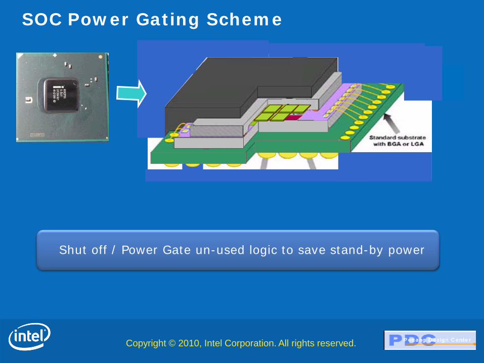
Shut off / Power Gate un-used logic to save stand-by power
SOC Power Gating Scheme
Copyright © 2010, Intel Corporation. All rights reserved.
Header Cell (PMOS)
To pkg, pcb, battery
From Power Management
Controller (PMC) Gated Vdd
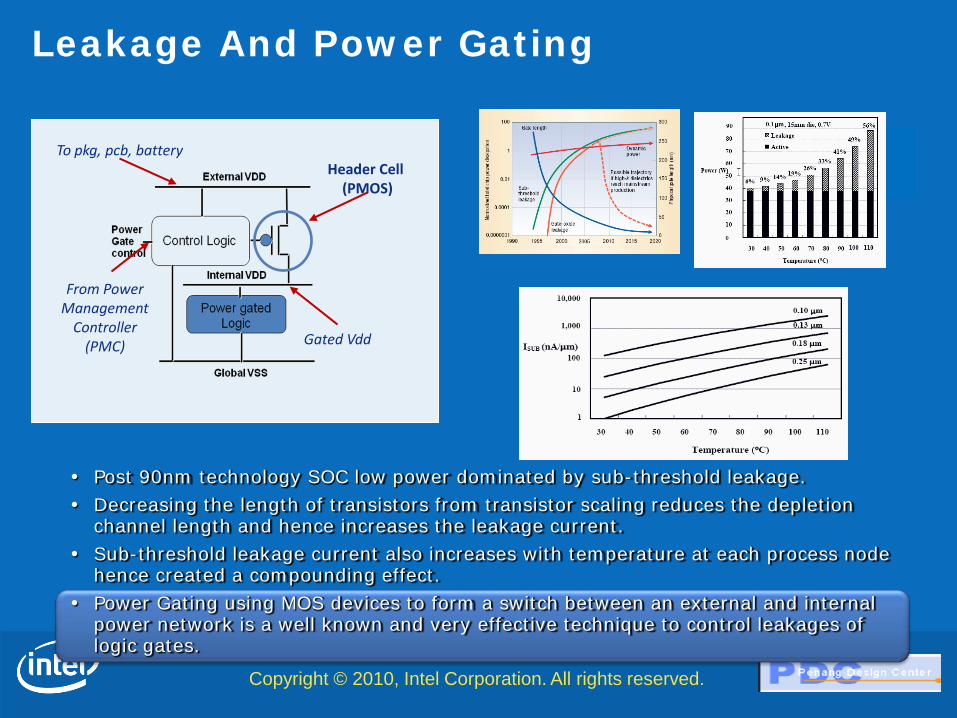
Post 90nm technology SOC low power dominated by sub-threshold leakage. Decreasing the length of transistors from transistor scaling reduces the depletion
channel length and hence increases the leakage current. Sub-threshold leakage current also increases with temperature at each process node
hence created a compounding effect. Power Gating using MOS devices to form a switch between an external and internal
power network is a well known and very effective technique to control leakages of logic gates.
Leakage And Power Gating
Copyright © 2010, Intel Corporation. All rights reserved.
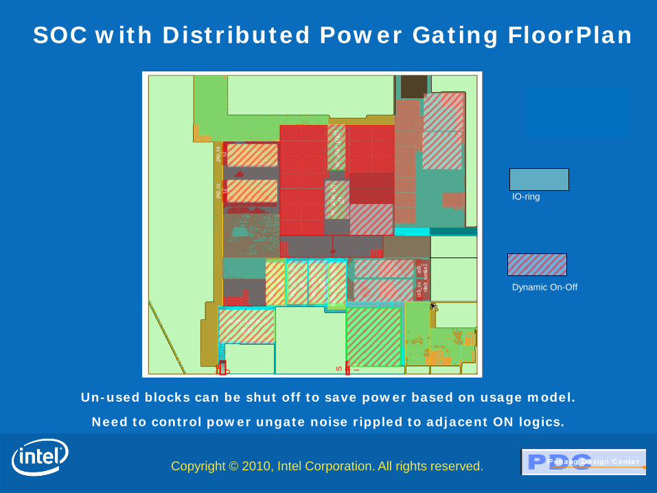
SOC with Distributed Power Gating FloorPlan
Un-used blocks can be shut off to save power based on usage model.
Need to control power ungate noise rippled to adjacent ON logics.
dby_
core
_pgd
1sa
ta_co
re_p
gd1
sata_
core
_pgd
2sa
ta_co
re_p
gd3
usb_
sus1
usb_
sus2
nvm_core_pgd1
usb_
sus3
pxp_
sus2
pxp_
sus2
ve_a
sw_p
gd1
ve_a
sw_p
gd2
CP
U S P I
Dynamic On-Off
IO-ring
Copyright © 2010, Intel Corporation. All rights reserved.
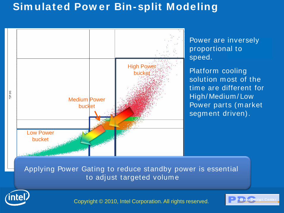
Simulated Power Bin-split Modeling
High Power bucket
Medium Power bucket
Low Power bucket
Power are inversely proportional to speed.
Platform cooling solution most of the time are different for High/Medium/Low Power parts (market segment driven).
Applying Power Gating to reduce standby power is essential to adjust targeted volume

Copyright © 2010, Intel Corporation. All rights reserved.
Power Integrity Design Challenges on Power Gating Implementation
Static IR drop
• On / Off stage
Dynamic Power Noise
• Instantaneous power ungate Noise
ST1ENBVcc
ST2ENB
VccVccST3ENB
PGDST1 PGDST2 PGDST3
Vcc
PGD2 . . .
CORE2ENB
V1ENBVccA
VEENB
VccAVccAV3ENB
PGDV1 PGDV2 PGDV3
VccA
PGDE . . .
EENB
ASW
PGDE
PGDV3
PGDV2
PGDV1
1.1
VASW
PGD2
PGDST3
PGDST2
PGDST1
VCCMIN = 0.93
Copyright © 2010, Intel Corporation. All rights reserved.
Agenda
• Introduction & background
• Power Gating Management Controller
• In-Rush Current Prediction
• Power Delivery Network Modeling
• Pre v.s. Post Silicon Correlation
• Summary and conclusion
Copyright © 2010, Intel Corporation. All rights reserved.
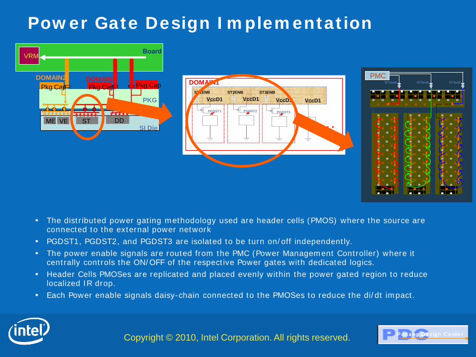
Power Gate Design Implementation
The distributed power gating methodology used are header cells (PMOS) where the source are connected to the external power network
PGDST1, PGDST2, and PGDST3 are isolated to be turn on/off independently. The power enable signals are routed from the PMC (Power Management Controller) where it
centrally controls the ON/OFF of the respective Power gates with dedicated logics. Header Cells PMOSes are replicated and placed evenly within the power gated region to reduce
localized IR drop. Each Power enable signals daisy-chain connected to the PMOSes to reduce the di/dt impact.
ST1ENB
VccD1ST2ENB
VccD1VccD1ST3ENB
PGDST1 PGDST2 PGDST3
. .
DOMAIN1
VccD1
ST DD
Pkg Cap Pkg Cap
ME
Pkg Cap
SI Die
Board
PKG
DOMAIN1DOMAIN2
. . .
VRM
VE
ST1enb ST2enb ST3enbPMC
Copyright © 2010, Intel Corporation. All rights reserved.
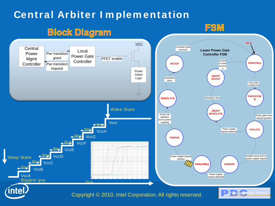
Central Arbiter Implementation
PWRSTBLE
PWROFFREQ
ISOLATE
PWROFFPWRUPREQ
PWRON
rst_b
Power gate condition met
Power gate entry request granted
Isolation done and no power ungate request
ABORTDEISOLATE
ABORTiRSTUP
Power ungate request detected
Deisolation done
Controller reset remove
d
Power ungate request detected
Power ungate requestgranted
DEISOLATE
Power rail stabilizes
due to power ungating
iRSTUP
Deisolation done
Controller reset removed Lower Power Gate
Controller FSMCentral Power Mgmt
Controller
Local Power Gate Controller
Pwr transition grant
Pwr transition request
Power Gated Logic
PFET enable
VCC
VccC
Biggest guy
8ns
VccA
VccB
VccD
VccF
VccGVccH
VccI
5us
Sleep State8ns
8ns
8ns
8ns
8ns
8ns8ns
Wake State
VccE
Copyright © 2010, Intel Corporation. All rights reserved.
Agenda
• Introduction & background
• Power gating Management Controller
• In-Rush Current Prediction
• Power Delivery Network Modeling
• Pre v.s. Post Silicon Correlation
• Summary and conclusion

Copyright © 2010, Intel Corporation. All rights reserved.
CPT Power Ungating Rush Current Design
STAGE1
Behavioral Model-75% Confident
-RTL based.
STAGE2
Physical Model-85% confident
-Physical placement and unrouted.
Delay
Delay values from8ns to 80ns
FINAL/ECO
Optimized Physical Model-95% confident
- Physical Optimized
Behavioral Modeling Physical Model Optimized Physical Model
Availability As soon RTL coded with Pfet instantiation and gated region gate count available
Post placement, unrouted DB. PreCTS PV. Manual overrides on daisy chain timing.
Post timing optimized. Physical Chain stitch timing propagated. Enable slope calculated from PT.
Accuracy 75%. Typical corner @ room temp only
85%. Fast & slow with Hot and cold
95%. Fast & slow with Hot and cold
Simulation Time 1-2 days 3-4 days 1 week +
Ease of integration to Pkg analysis
same same same
Copyright © 2010, Intel Corporation. All rights reserved.
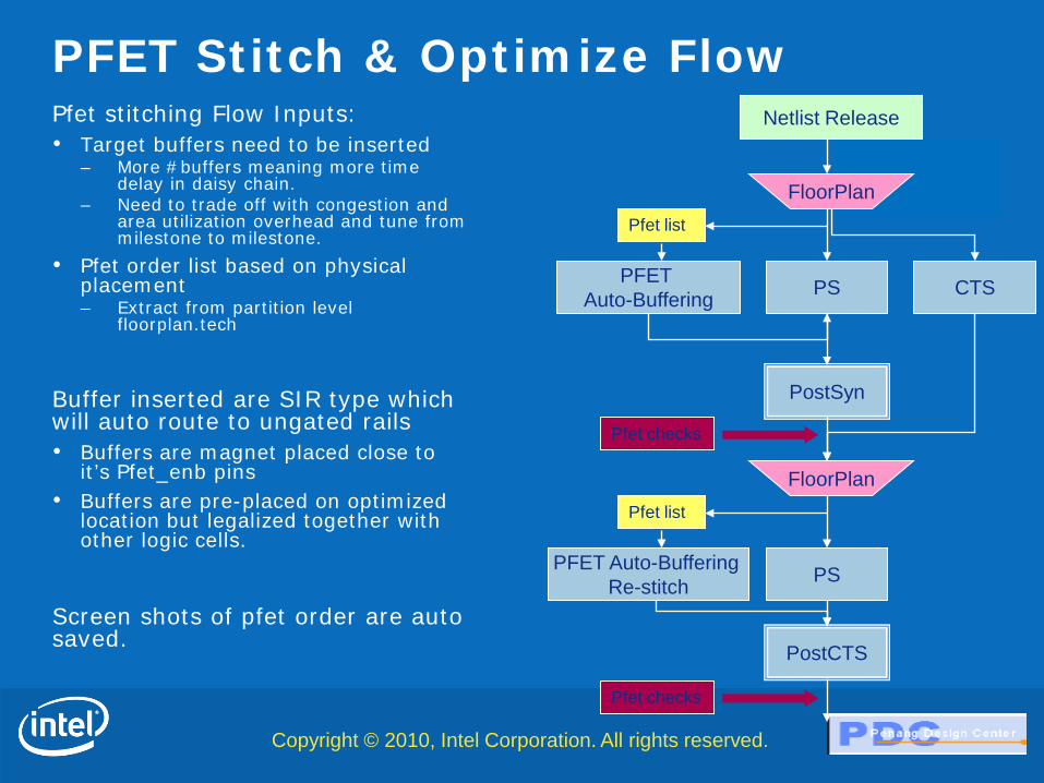
PFET Stitch & Optimize FlowPfet stitching Flow Inputs:• Target buffers need to be inserted
– More #buffers meaning more time delay in daisy chain.
– Need to trade off with congestion and area utilization overhead and tune from milestone to milestone.
• Pfet order list based on physical placement – Extract from partition level
floorplan.tech
Buffer inserted are SIR type which will auto route to ungated rails• Buffers are magnet placed close to
it’s Pfet_enb pins• Buffers are pre-placed on optimized
location but legalized together with other logic cells.
Screen shots of pfet order are auto saved.
Netlist Release
FloorPlan
PS CTS
PostSyn
PostCTS
PFET Auto-Buffering
Pfet list
FloorPlan
PFET Auto-Buffering Re-stitch
Pfet list
PS
Pfet checks
Pfet checks
Copyright © 2010, Intel Corporation. All rights reserved.
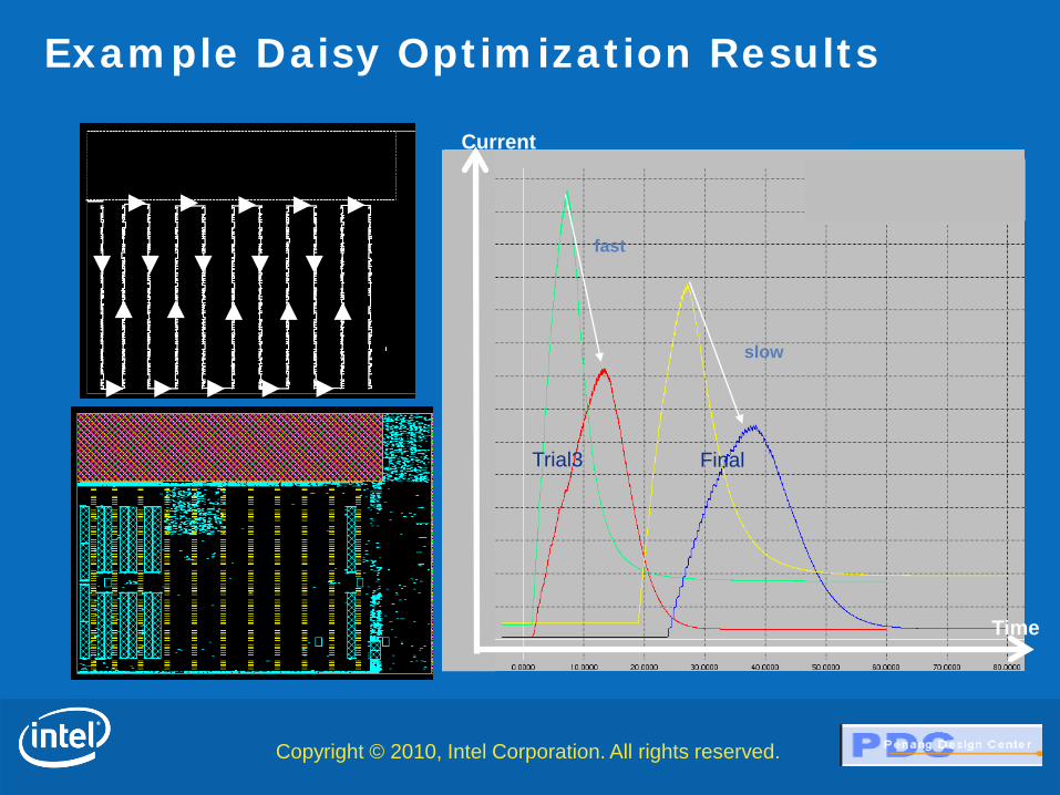
Example Daisy Optimization Results
Trial3 Final
fast
slow
Current
Time

Copyright © 2010, Intel Corporation. All rights reserved.
Agenda
• Introduction & background
• Power gating Management Controller
• In-Rush Current Prediction
• Power Delivery Network Modeling
• Pre v.s. Post Silicon Correlation
• Summary and conclusion
Copyright © 2010, Intel Corporation. All rights reserved.
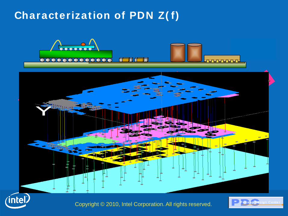
Characterization of PDN Z(f)
Copyright © 2010, Intel Corporation. All rights reserved.
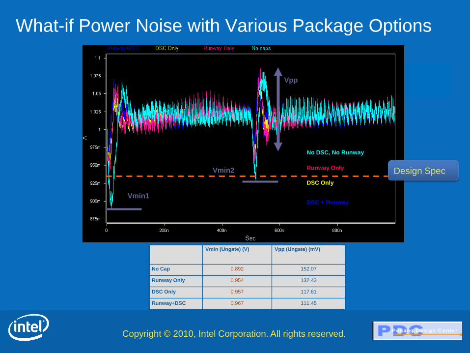
What-if Power Noise with Various Package Options
Vmin1
Vpp
No DSC, No Runway
DSC + Runway
Runway Only
DSC Only
Vmin2
Vmin (Ungate) (V) Vpp (Ungate) (mV)
No Cap 0.892 152.07
Runway Only 0.954 132.43
DSC Only 0.957 117.61
Runway+DSC 0.967 111.45
Design Spec
Copyright © 2010, Intel Corporation. All rights reserved.
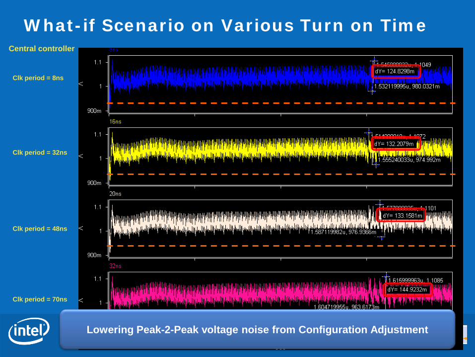
What-if Scenario on Various Turn on TimeCentral controller
Clk period = 8ns
Clk period = 32ns
Clk period = 48ns
Clk period = 70ns
Lowering Peak-2-Peak voltage noise from Configuration Adjustment

Copyright © 2010, Intel Corporation. All rights reserved.
Agenda
• Introduction & background
• Power gating Management Controller
• In-Rush Current Prediction
• Power Delivery Network Modeling
• Pre v.s. Post Silicon Correlation
• Summary and conclusion
Copyright © 2010, Intel Corporation. All rights reserved.
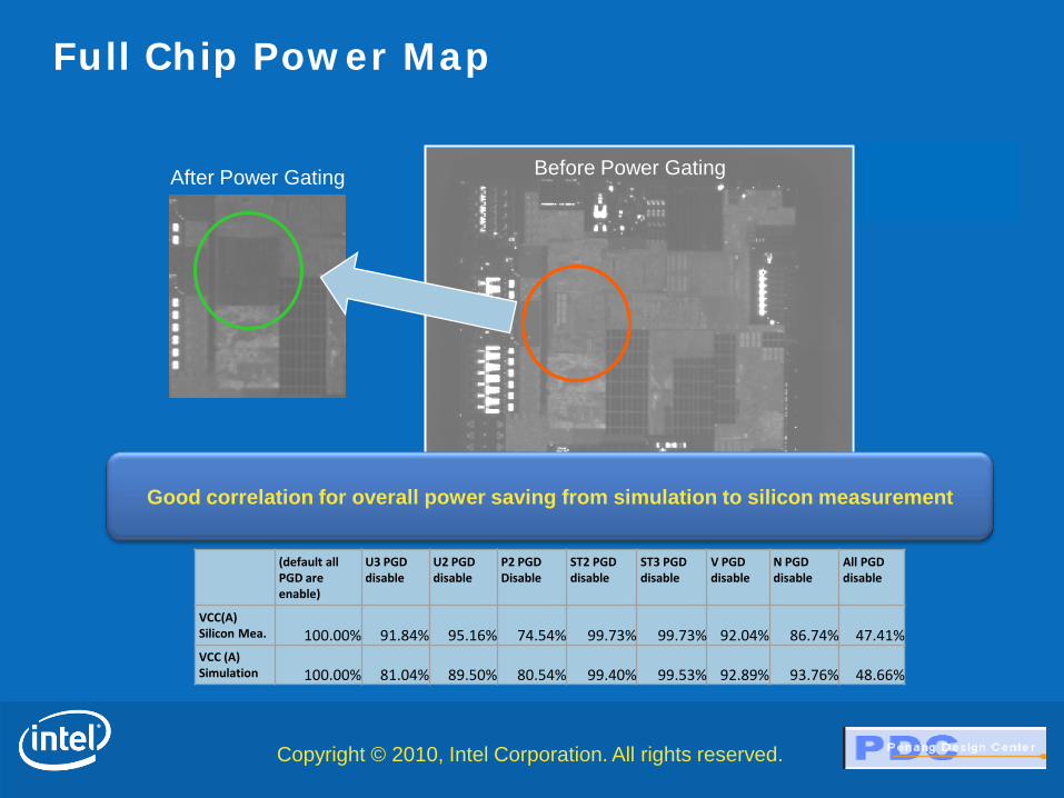
Full Chip Power Map
(default all PGD are enable)
U3 PGD disable
U2 PGD disable
P2 PGDDisable
ST2 PGD disable
ST3 PGD disable
V PGD disable
N PGD disable
All PGD disable
VCC(A) Silicon Mea. 100.00% 91.84% 95.16% 74.54% 99.73% 99.73% 92.04% 86.74% 47.41%VCC (A)Simulation 100.00% 81.04% 89.50% 80.54% 99.40% 99.53% 92.89% 93.76% 48.66%
Infrared Emission Microscope
Before Power Gating After Power Gating
Good correlation for overall power saving from simulation to silicon measurement

Copyright © 2010, Intel Corporation. All rights reserved. 3/5/2011
22
Measurement Setup
1. Test probe pads are prepared on package
2. On package Probing needs Micro-Probing system (Camera Video with Arm Station)
3. 2-Port VNA Micro Probe setup for Cdie Measurement
4. High bandwidth and High Impedance Scope

Copyright © 2010, Intel Corporation. All rights reserved.
On-Die Voltage Sampling Methodology
VCC, Gated: Voltage sampling is done by placing an inverter with input tide low (output driven High) with-in the
high IR drop risk region. No buffering on output signals to MUX at IO MUX select are programmed through DFT register via JTAG interface. MUX output signal are traced out at board and probed with High Impedance Scope.
VCC, Ungated: Package Trace out with test landing zone for probing at package level.
Silicon Measurement Setup
[0:29]30-to-1 MUX JTAG
Interface
To High Impedance Scope observability
SUS
CORE
SUSAW
CORE-PG
CORE
With Internal Pwr Gating
AW - PG
Board PS
SUS
CORE
PFET
PFET
VR
CORE-PGCORE-PGCORE-PGCORE-PGPFET
PFET
PFET
PFET
Probe Point

Copyright © 2010, Intel Corporation. All rights reserved.
0
2
4
6
8
10
12
14
OFF stage VCCg (mV) slow@100
OFF stage VCCg (mV) tt@25
OFF stage VCCg (mV) fast@0
Silicon Correlation – VCC,Gated Power Up
05
10152025303540
ON IR drop (mV) slow@100
ON IR drop (mV) tt@25
ON IR drop (mV) fast@0 0.00E+00
2.00E-01
4.00E-01
6.00E-01
8.00E-01
1.00E+00
1.20E+00
011000
22000
33000
44000
55000
66000
77000
88000
99000
110000
121000
132000
143000
154000
Vg
ate
d (
V)
Power up Sim2Sil Correlation
Silicon Measurement
Simulation
Copyright © 2010, Intel Corporation. All rights reserved.
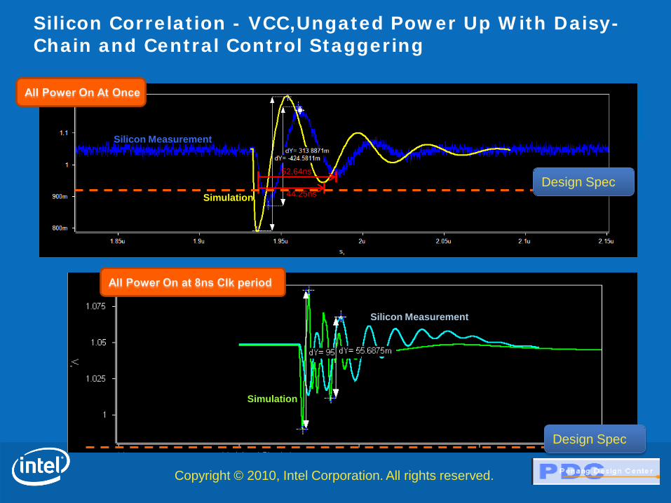
Silicon Correlation - VCC,Ungated Power Up With Daisy-Chain and Central Control Staggering
Silicon Measurement
Simulation
52.64ns
44.25nsDesign Spec
Design Spec
Silicon Measurement
Simulation

Copyright © 2010, Intel Corporation. All rights reserved.
Putting It All Together…
Design Spec
10X Reduction in effective Peak-2-Peak Voltage Noise

Copyright © 2010, Intel Corporation. All rights reserved.
Agenda
• Introduction & background
• Power gating Management Controller
• In-Rush Current Prediction
• Power Delivery Network Modeling
• Pre v.s. Post Silicon Correlation
• Summary and conclusion

Copyright © 2010, Intel Corporation. All rights reserved.
Summary and Conclusion
• To save power, many SOC products are employing Power Gating within its core partition. It causes – increase in DC IR drop – power un-gating events cause sufficiently large power delivery noise droop
• This paper presented a complete design and analysis methodology and presents the simulation results for a low power design starting from early planning stage to physical implementation.
• Performance improvements of about 10X were seen through the design optimizations.
• Various Design techniques has been successfully presented to scale the di/dt to meet performance goal.
• This paper has successfully illustrated a comprehensive top down design methodology to enforce power savings on a computing system; which could be leveraged across the industry aiming with similar interest.
• Last but not least, the post-silicon validation data has shown a very good match to as close as 96% correlation
Copyright © 2010, Intel Corporation. All rights reserved.
Next Step
Enhance detail on-die Cap modeling especially the substrate Cap which causes the rise time discrepancy. Investigate on more details 3D package modeling instead
of Quasi-static 2.5D model. Investigate on AC voltage droop to timing impact during
power ungate event on Always on logics.

Thank you
Copyright © 2010, Intel Corporation. All rights reserved.
Acknowledgement
Thanks to all members of the project team who has contributed directly or indirectly to the success of the PCH core current development method
Copyright © 2010, Intel Corporation. All rights reserved.
Legal Disclaimer
No computer system can provide absolute security under all conditions. Intel® Trusted Execution Technology (Intel® TXT) requires a computer system with Intel® Virtualization Technology, an Intel TXT-enabled processor, chipset, BIOS, Authenticated Code Modules and an Intel TXT-compatible measured launched environment (MLE). The MLE could consist of a virtual machine monitor, an OS or an application. In addition, Intel TXT requires the system to contain a TPM v1.2, as defined by the Trusted Computing Group and specific software for some uses. For more information, see http://www.intel.com/technology/security.
Intel and the Intel logo is a trademark or registered trademark of Intel Corporation or its subsidiaries in the United States and other countries.
Performance tests and ratings are measured using specific computer systems and/or components and reflect the approximate performance of products as measured by those tests. Any difference in system hardware or software design or configuration may affect actual performance.
Intel does not control or audit the design or implementation of third party benchmark data or Web sites referenced in this document. Intel encourages all of its customers to visit the referenced Web sites or others where similar performance benchmark data are reported and confirm whether the referenced benchmark data are accurate and reflect performance of systems available for purchase.
*Other names and brands may be claimed as the property of others.