Embed Size (px)
Citation preview

Copyright Cirrus Logic, Inc. 2015–2017(All Rights Reserved)
http://www.cirrus.com
130-dB, 32-Bit High-Performance DAC with Integrated Headphone Driver and Impedance Detection
System Features• Enhanced oversampling DAC architecture
— 32-bit resolution— Up to 384-kHz sampling rate— Low clock jitter sensitivity— Auto mute detection
• Integrated high performance, ground-centered stereo headphone outputs— 130-dB dynamic range (A-weighted)— –115-dB total harmonic distortion + noise (THD+N)— 110-dB interchannel isolation— Up to 2-Vrms stereo output— Headphone power output
– 30 mW per channel into 32 – 5 mW per channel into 600
• Headphone detection— Headphone DC and AC impedance measurement— Headphone plug-in detection— Popguard® technology eliminates pop noise
• Integrated PLL— Support for 11.2896-/22.5792-, 12.288-/24.576-, 9.6-/
19.2-, 12-/24-, and 13-/26-MHz system MCLK rates— Reference clock sourced from XTI/MCLK pin— System clock output
• Mono Mode (differential) support • I2C control—up to 1 MHz• Wideband Flatness Mode Support
• Direct Stream Digital (DSD®) path— Up to 256•Fs DSD— Patented DSD processor
– On-chip 50-kHz filter to meet Scarlet Book Super Audio Compact Disk (SACD) recommendations
– Matched PCM and DSD analog output levels– Nondecimating volume control with 0.5-dB step size
and soft ramp– DSD and Pulse-code modulation (PCM) mixing for
alerts— Dedicated DSD and DoP pin interface
• Serial audio input path— Programmable Hi-Fi digital filter— Five selectable digital filter responses
– Low-latency Mode minimizes pre-echo– 110 dB of stopband attenuation
— Supports sample rates from 32 to 384 kHz— I2S, right-justified, left-justified, TDM, and
DSD-over-PCM (DoP) interface— Master or slave operation— Volume control with 0.5-dB step size and soft ramp— 44.1 kHz deemphasis and inverting feature
• Alternate headphone input• 40-pin 5mm × 5mm QFN or 42-ball CSP package options
Applications• Smart phones, tablets, portable media players, laptops,
digital headphones, powered speakers, AVR, home theater systems, Blu-ray/DVD/SACD players, and pro audio
VCP_FILT+
InterpolationFilter and Volume Control
DSD Processor
InterpolationFilter and Volume Control
Control Port Level TranslatorRegister /Hardware
Configuration
PLL
XTI/MCLK
DoP to DSD
Engine
Analog Supply (VA,VCP)
+1.8VFILT+
Leve
l T
ran
slat
or
Popguard®Circuitry
FLYN _VCP
DAC and Filter
DAC and Filter
FLYP_VA
HP_DETECT
XTALOSC
XTO–
+
VCP_FILT +
VCP_FILT-
–
+
HPINB
HPINA
FLYN_VA-VA
Charge PumpInterruptSources
InternalVoltage
Reference
HPOUTA
HPOUTB
HPREFBHPREFA
MU
X
FILT-
FLYP_VCP
VA
-VA
VA
-VA
Dig
ital A
udio
Bus FLYC_VCP
Battery Supply (VP)
VCP_FILT-
VCP_FILT+
VCP_FILT -
RESET
CLKOUT
Digital LDOs
Digital Core
Interface Supply (VL)
+1.8V
Internal Supply (VD)
+1.8V
HP Detect, HP Impedance
Detect and Measure
TSO
ASP
XSP/DSD Audio
Interface
SCLK1
LRCK1
SDIN1
DSDA/SDIN2
Multibit
Modulator
Multibit
Modulator
INT
ADR SDA SCL
DSDCLK/SCLK2
DSDB/LRCK2
DS1155F1OCT ’17
CS43131
2 DS1155F1
CS43131
General DescriptionThe CS43131 is a high-performance, 32-bit resolution, stereo audio DAC that supports up to 384-kHz sampling frequency with integrated low-noise ground-centered headphone amplifiers. The advanced 32-bit oversampled multibit modulator with mismatch shaping technology eliminates distortion due to on-chip component mismatch. Proprietary digital-interpolation filters support five selectable filter responses with pseudo-linear phase and ultralow latency to minimize pre-echos and ringing artifacts. An on-chip programmable filter is available for further response customization. Other features include volume control with 0.5-dB steps, wideband flatness mode support, and digital deemphasis for 44.1-kHz sample rate.
The integrated ground-centered stereo headphone amplifiers are capable of delivering more than 30 mW into 32- load or 5 mW into 600- load per channel at full performance. It is also capable of generating 2 Vrms on a 600- load. Proprietary headphone impedance detection enables wide-band impedance detection for further digital post-processing. An internal stereo audio switch with true bypass supports an alternate analog input path for interfacing with external audio sources to minimize the overall bill-of-materials cost and PCB area.
The patented on-chip DSD processor preserves audio integrity by allowing signal processing such as volume control and 50-kHz Scarlet Book recommended filtering to be applied directly to the DSD stream without an intermediate decimation stage. Additional features like volume matching and channel mixing enable seamless transition between DSD and PCM playback paths.
The CS43131 accepts I2S, right-justified, left-justified, and TDM-format PCM data at sample rates from 32 to 384 kHz. The industry-standard high-speed I2C interface capable of up to 1-MHz operation provides easy configuration control. An integrated PLL allows for maximum clocking flexibility in any system. Popguard® technology eliminates output transients upon power-up or power-down events.
The CS43131 is available in a commercial-grade 42-ball WLCSP or 40-pin QFN package for operation from –10°C to +70°C.
DS1155F1 3
CS43131
Table of Contents
1 Pin Assignments and Descriptions . . . . . . . . . . . . . . . . . . . . . . 41.1 40-Pin QFN (Top-Down, Through-Package View) . . . . . . . . . 41.2 42-Ball WLCSP (Top-down, Through-Package View) . . . . . . 51.3 Pin Descriptions . . . . . . . . . . . . . . . . . . . . . . . . . . . . . . . . . . . 61.4 Electrostatic Discharge (ESD) Protection Circuitry . . . . . . . . 8
2 Typical Connection Diagram . . . . . . . . . . . . . . . . . . . . . . . . . . 103 Characteristics and Specifications . . . . . . . . . . . . . . . . . . . . . 12
Table 3-1. Parameter Definitions . . . . . . . . . . . . . . . . . . . . . . . . 12Table 3-2. Recommended Operating Conditions . . . . . . . . . . . 12Table 3-3. Absolute Maximum Ratings . . . . . . . . . . . . . . . . . . 13Table 3-4. Analog Output Characteristics (HV_EN = 1) . . . . . 13Table 3-5. Analog Output Characteristics (HV_EN = 0) . . . . . 15Table 3-6. Wideband Flatness Mode Analog Output
Characteristics . . . . . . . . . . . . . . . . . . . . . . . . . . . . . . . . . . . . 17Table 3-7. Headphone Load Measurement . . . . . . . . . . . . . . . 18Table 3-8. Alternate Headphone Path . . . . . . . . . . . . . . . . . . . 19Table 3-9. Combined DAC Digital, On-Chip Analog and
HPOUTx Filter Characteristics . . . . . . . . . . . . . . . . . . . . . . . . 19Table 3-10. Combined DAC Digital, On-Chip Analog and
HPOUTx Filter Characteristics (Wideband Flatness Mode) . . 21Table 3-11. DAC High-Pass Filter (HPF) Characteristics . . . . . 21Table 3-12. DSD Combined Digital and On-Chip Analog Filter
Response . . . . . . . . . . . . . . . . . . . . . . . . . . . . . . . . . . . . . . . . 22Table 3-13. Digital Interface Specifications and Characteristics 22Table 3-14. CLKOUT Characteristics . . . . . . . . . . . . . . . . . . . . 22Table 3-15. PLL Characteristics . . . . . . . . . . . . . . . . . . . . . . . . 22Table 3-16. Crystal Characteristics . . . . . . . . . . . . . . . . . . . . . 23Table 3-17. Power-Supply Rejection Ratio (PSRR)
Characteristics . . . . . . . . . . . . . . . . . . . . . . . . . . . . . . . . . . . . . 23Table 3-18. DC Characteristics . . . . . . . . . . . . . . . . . . . . . . . . 24Table 3-19. Power Consumption . . . . . . . . . . . . . . . . . . . . . . . 24Table 3-20. Serial-Port Interface Characteristics . . . . . . . . . . . 24Table 3-21. DSD Switching Characteristics . . . . . . . . . . . . . . . 25Table 3-22. I2C Slave Port Characteristics . . . . . . . . . . . . . . . . 26
4 Functional Description . . . . . . . . . . . . . . . . . . . . . . . . . . . . . . . 284.1 Overview . . . . . . . . . . . . . . . . . . . . . . . . . . . . . . . . . . . . . . . 284.2 Analog Outputs . . . . . . . . . . . . . . . . . . . . . . . . . . . . . . . . . . . 314.3 Class H Amplifier Output . . . . . . . . . . . . . . . . . . . . . . . . . . . 324.4 Alternate Headphone Inputs . . . . . . . . . . . . . . . . . . . . . . . . . 374.5 Headphone Presence Detect and Output Load Detection . . 384.6 Clocking Architecture . . . . . . . . . . . . . . . . . . . . . . . . . . . . . . 414.7 Clock Output and Fractional-N PLL . . . . . . . . . . . . . . . . . . . 444.8 Filtering Options . . . . . . . . . . . . . . . . . . . . . . . . . . . . . . . . . . 464.9 Audio Serial Port (ASP) . . . . . . . . . . . . . . . . . . . . . . . . . . . . 474.10 DSD Interface . . . . . . . . . . . . . . . . . . . . . . . . . . . . . . . . . . . 554.11 DSD and PCM Mixing . . . . . . . . . . . . . . . . . . . . . . . . . . . . 574.12 Standard Interrupts . . . . . . . . . . . . . . . . . . . . . . . . . . . . . . . 574.13 Control Port Operation . . . . . . . . . . . . . . . . . . . . . . . . . . . . 594.14 Programmable Filter . . . . . . . . . . . . . . . . . . . . . . . . . . . . . . 62
5 Applications . . . . . . . . . . . . . . . . . . . . . . . . . . . . . . . . . . . . . . . . 635.1 PLL Clocking . . . . . . . . . . . . . . . . . . . . . . . . . . . . . . . . . . . . 635.2 Power Sequencing . . . . . . . . . . . . . . . . . . . . . . . . . . . . . . . . 635.3 Crystal Tuning . . . . . . . . . . . . . . . . . . . . . . . . . . . . . . . . . . . 635.4 Alert Mixing Shutdown . . . . . . . . . . . . . . . . . . . . . . . . . . . . . 645.5 Enable/Disable Alternate Headphone Path (HPINx) . . . . . . 645.6 Headphone Power Down Sequences . . . . . . . . . . . . . . . . . 655.7 Headphone Power-Up Sequence . . . . . . . . . . . . . . . . . . . . . 665.8 Power-Down Sequence in External VCPFILT Mode . . . . . . 675.9 Enabling and Disabling NOS Filter . . . . . . . . . . . . . . . . . . . . 695.10 Sequence for Using PCM Invert Bits . . . . . . . . . . . . . . . . . 705.11 Sequences for Using the PCM Channel Swap Bit . . . . . . . 725.12 Sequences for Enabling and Disabling Mono Mode
for PCM Playback . . . . . . . . . . . . . . . . . . . . . . . . . . . . . . . . . . . 735.13 Example Sequences . . . . . . . . . . . . . . . . . . . . . . . . . . . . . 745.14 Headphone Load Measurement . . . . . . . . . . . . . . . . . . . . . 99
6 Register Quick Reference . . . . . . . . . . . . . . . . . . . . . . . . . . . . 1066.1 Global Registers . . . . . . . . . . . . . . . . . . . . . . . . . . . . . . . . . 1066.2 PLL Registers . . . . . . . . . . . . . . . . . . . . . . . . . . . . . . . . . . . 1066.3 ASP and XSP Registers . . . . . . . . . . . . . . . . . . . . . . . . . . . 1076.4 DSD Registers . . . . . . . . . . . . . . . . . . . . . . . . . . . . . . . . . . 1086.5 Headphone and PCM Registers . . . . . . . . . . . . . . . . . . . . . 1096.6 Interrupt Status and Mask Registers . . . . . . . . . . . . . . . . . 112
7 Register Descriptions . . . . . . . . . . . . . . . . . . . . . . . . . . . . . . . 1137.1 Global Registers . . . . . . . . . . . . . . . . . . . . . . . . . . . . . . . . . 1137.2 PLL Registers . . . . . . . . . . . . . . . . . . . . . . . . . . . . . . . . . . . 1167.3 ASP and XSP Registers . . . . . . . . . . . . . . . . . . . . . . . . . . . 1187.4 DSD Registers . . . . . . . . . . . . . . . . . . . . . . . . . . . . . . . . . . 1247.5 Headphone and PCM Registers . . . . . . . . . . . . . . . . . . . . 1277.6 Interrupt Status and Mask Registers . . . . . . . . . . . . . . . . . 134
8 PCB Layout Considerations . . . . . . . . . . . . . . . . . . . . . . . . . . 1408.1 Power Supply . . . . . . . . . . . . . . . . . . . . . . . . . . . . . . . . . . . 1408.2 Grounding . . . . . . . . . . . . . . . . . . . . . . . . . . . . . . . . . . . . . . 1408.3 HPREFA and HPREFB Routing . . . . . . . . . . . . . . . . . . . . . 1408.4 QFN Thermal Pad . . . . . . . . . . . . . . . . . . . . . . . . . . . . . . . 140
9 Performance Plots . . . . . . . . . . . . . . . . . . . . . . . . . . . . . . . . . . 1419.1 Digital Filter Response . . . . . . . . . . . . . . . . . . . . . . . . . . . . 141
10 Package Dimensions . . . . . . . . . . . . . . . . . . . . . . . . . . . . . . . 15310.1 40-Pin QFN Package Dimensions . . . . . . . . . . . . . . . . . . 15310.2 42-Ball WLCSP Package Dimensions . . . . . . . . . . . . . . . 154
11 Thermal Characteristics . . . . . . . . . . . . . . . . . . . . . . . . . . . . 15512 Ordering Information . . . . . . . . . . . . . . . . . . . . . . . . . . . . . . . 15513 References . . . . . . . . . . . . . . . . . . . . . . . . . . . . . . . . . . . . . . . 15514 Revision History . . . . . . . . . . . . . . . . . . . . . . . . . . . . . . . . . . . 155
4 DS1155F1
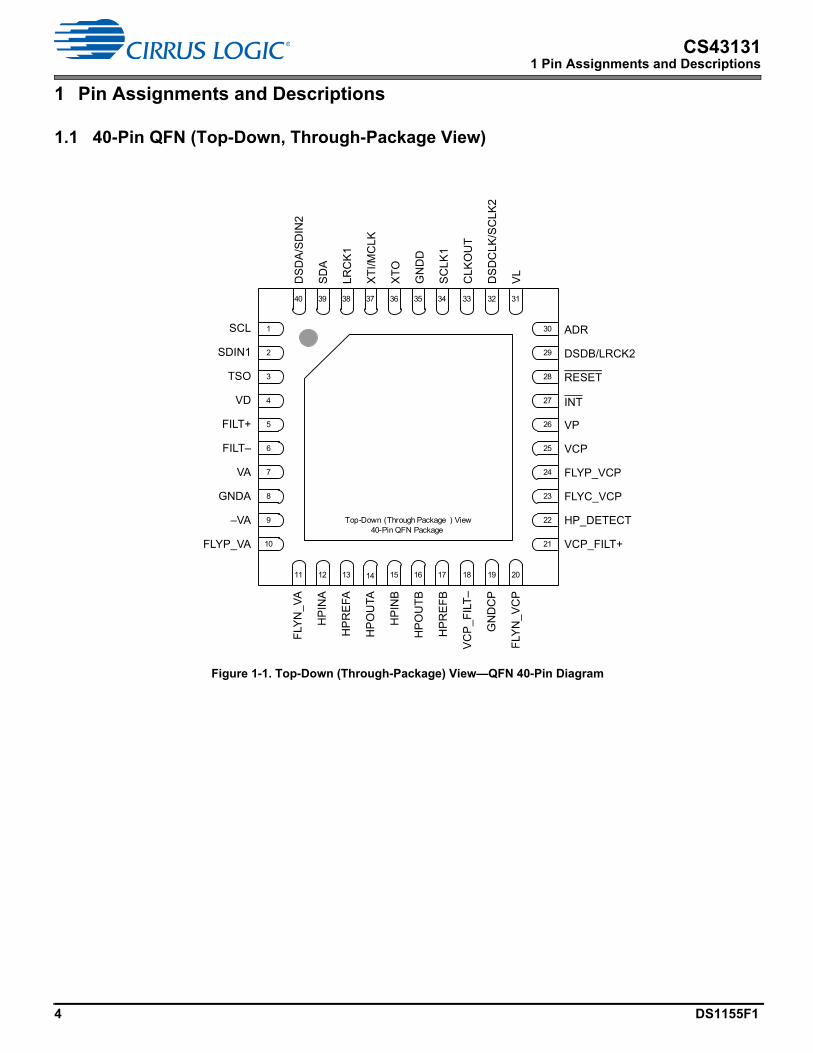
CS431311 Pin Assignments and Descriptions
1 Pin Assignments and Descriptions
1.1 40-Pin QFN (Top-Down, Through-Package View)
Figure 1-1. Top-Down (Through-Package) View—QFN 40-Pin Diagram
Top-Down (Through Package ) View40-Pin QFN Package
21
26
27
28
29
30
22
23
24
25
7
6
5
4
3
2
1
10
9
8
1211 13 14 15 16 17 18 19 20
3940 38 37 36 35 34 33 32 31
DSDB/LRCK2
RESET
VCP
FLYP_VCP
FLYC_VCP
HP_DETECT
VCP_FILT+
SCL
SDIN1
TSO
VD
FILT+
FILT–
VA
GNDA
–VA
FLYP_VA
DS
DA
/SD
IN2
SD
A
LR
CK
1
XT
I/M
CL
K
XT
O
GN
DD
SC
LK
1
CLK
OU
T
DS
DC
LK/S
CLK
2
HP
RE
FA
HP
OU
TA
HP
INB
HP
OU
TB
HP
RE
FB
VC
P_F
ILT
–
INT
VP
VL
ADR
GN
DC
P
FLY
N_
VC
P
FLY
N_V
A
HP
INA

DS1155F1 5
CS431311.2 42-Ball WLCSP (Top-down, Through-Package View)
1.2 42-Ball WLCSP (Top-down, Through-Package View)
Figure 1-2. Top-Down (Through-Package) View—42-Ball WLCSP Package
VL SCLK1 XTO XTI/MCLK DSDA/SDIN2
SDIN1
DSDCLK/SCLK2
CLKOUT LRCK1 SDA SCL TSO
DSDB/LRCK2
ADR GNDD RESET INT VD
VP VCP TSI FILT+ FILT– VA
FLYP_VCP VCP_FILT+ HPREFB HPREFA GNDA –VA
FLYC_VCP GNDCP HPINB HP_DETECT TSI FLYP_VA
FLYN_VCP VCP_FILT– HPOUTB HPOUTA HPINA FLYN_VA
A1 A2 A3 A4 A5 A6
B1 B2 B3 B4 B5 B6
C1 C2 C3 C4 C5 C6
D1 D2 D3 D4 D5 D6
E1 E2 E3 E4 E5 E6
F1 F2 F3 F4 F5 F6
G1 G2 G3 G4 G5 G6
Charge Pump Analog I/O Digital I/OGround Power Supplies Test

6 DS1155F1
CS431311.3 Pin Descriptions
1.3 Pin Descriptions
Table 1-1. Pin Descriptions
Pin NameQFN Pin #
WLCSPBall
PowerSupply
I/O Pin DescriptionInternal
ConnectionDigital I/O
DriverDigital I/O Receiver
ADR 30 C2 VL I Address Bit (I²C). In I²C Mode, ADR is a chip address pin. — — —CLKOUT 33 B2 VL O CLK Output. Single-ended clock output sourced from PLL or
buffered crystal. Weak
pull-downCMOS output
—
SCLK1 34 A2 VL I/O Serial Audio Input Bit Clock 1. Serial bit clock for audio data on the SDIN pins.
Weak pull-down
CMOS output
Hysteresis on CMOS
inputLRCK1 38 B3 VL I/O Serial Audio Input Left/Right Clock. Word-rate clock for the
audio data on the SDIN pins.Weak
pull-downCMOS output
Hysteresis on CMOS
inputSDIN1 2 A6 VL I Serial Audio Input Data Port. Audio data serial input pin 1. Weak
pull-down— Hysteresis
on CMOS input
DSDA/SDIN2
40 A5 VL I DSD Data Input A/Serial Data In 2. DSD audio or PCM audio data serial input pin 2.
Weak pull-down
— Hysteresis on CMOS
inputDSDB/LRCK2
29 C1 VL I/O DSD Data Input B/Serial Audio Input Left/Right Clock 2. DSD audio data serial input pin or word rate clock for the audio data on the SDIN2 pin.
Weak pull-down
CMOS output
Hysteresis on CMOS
inputDSDCLK/
SCLK232 B1 VL I/O DSD Clock Input/Serial Audio Input Bit Clock 2. DSD clock
input. Serial bit clock for audio data on the SDIN2 pin. Weak
pull-downCMOS output
Hysteresis on CMOS
input
INT 27 C5 VP O Interrupt. When pulled up, works as system interrupt pin. Open drain, active low programmable.
— CMOS open-drain
output
—
RESET 28 C4 VP I System Reset. The device enters system reset when enabled. — — Hysteresis on CMOS
inputSDA 39 B4 VL I/O Serial Control Data I/O (I²C). In I²C Mode, SDA is the control I/O
data line.— CMOS
open-drain output
Hysteresis on CMOS
inputSCL 1 B5 VL I Software Clock (I²C). Serial control interface clock used to clock
control data bits into and out of the CS43131.— — Hysteresis
on CMOS input
XTI/MCLK 37 A4 VL I Crystal/Oscillator Input/MCLK In. Crystal or digital clock input for the master clock.
Weak pull-down
— Hysteresis on CMOS
inputXTO 36 A3 VL O Crystal/Oscillator Output. Crystal output. Weak
pull-downCMOS output
—
FILT+FILT–
56
D4D5
VA O Positive/Negative Voltage Reference. Positive/negative reference voltage for DAC.
— — —
HP_DETECT
22 F4 VP I Headphone Detect. Can be configured to be debounced on unplugged and plugged events before it is presented as a noninterrupt status bit (HPDETECT).
— Hi-Z —
HPINBHPINA
1512
F3G5
VCP_FILT±
I Headphone Audio Input. For interfacing low power audio source, an alternate analog input path for the headphone output. Refer to analog specification table for full-scale input level.
Weak pull-down
— —
HPOUTBHPOUTA
1614
G3G4
VCP_FILT±
O Headphone Audio Output. Refer to analog specification table for full-scale output level.
— — —
HPREFBHPREFA
1713
E3E4
VCP_FILT±
I Headphone Output Reference. Reference for headphone amplifier and detect.
— — —
VL 31 A1 N/A I Logic Power. Input/Output power supply, typically +1.8 V. — — —VD 4 C6 N/A I Internal Digital Power. Internal digital power supply, typically
+1.8 V. — — —
VA 7 D6 N/A I Analog Power. Power supply for the internal analog section. — — —
Digital I/O
Analog I/O
Power Supplies

DS1155F1 7
CS431311.3 Pin Descriptions
VCP 25 D2 N/A I Charge Pump Supply. Provides charge pump voltage to the headphone Class H analog output circuit.
— — —
VP 26 D1 N/A I Battery supply. Provides voltage to the headphone Class H circuit.
— — —
GNDD 35 C3 N/A I Digital and I/O Ground. Ground for the I/O and core logic. GNDA, GNDCP, and GNDD must be connected to a common ground area under the chip.
— — —
GNDA 8 E5 N/A I Analog Ground. Ground reference for the internal analog section. GNDA, GNDCP, and GNDD must be connected to a common ground area under the chip.
— — —
GNDCP 19 F2 N/A I Charge Pump Ground. Ground reference for the charge pump section. GNDA, GNDCP, and GNDD must be connected to a common ground area under the chip.
— — —
VCP_FILT+VCP_FILT–
2118
E2G2
VCP/VP 1
I/O Inverting Charge Pump Filter Connection. Power supply from the inverting charge pump that provides the positive/negative rail for the analog output. When operating in external VCP_FILT mode, these pins can directly take in supply voltage.
— — —
–VA 9 E6 VA O VA Negative Charge Pump Output. Negative charge pump output for DAC rail. It is derived from VA.
— — —
FLYP_VAFLYN_VA
1011
F6G6
VA O –VA Charge Pump Cap Positive/Negative Node. Positive/negative nodes for the DAC negative charge pump’s flying capacitor.
— — —
FLYP_VCP 24 E1 VCP/VP 1
O –VCP Charge Pump Cap Positive Node. Positive node for the analog output negative charge pump’s flying capacitor.
— — —
FLYC_VCP 23 F1 VCP/VP 1
O –VCP Charge Pump Cap Center Node. Center node for the analog output negative charge pump’s flying capacitor.
— — —
FLYN_VCP 20 G1 VCP_FILT±
O –VCP Charge Pump Cap Negative Node. Negative node for the analog output negative charge pump’s flying capacitor.
— — —
TSO 3 B6 N/A I/O Test Output. — — —TSI — D3, F5 Test Input. — — —
1.The power supply is determined by ADPT_PWR setting (see Section 4.3.1). VP is used if ADPT_PWR = 001 (VP_LDO Mode) or when necessary for ADPTPWR = 111 (Adapt-to-Signal Mode).
Table 1-1. Pin Descriptions (Cont.)
Pin NameQFN Pin #
WLCSPBall
PowerSupply
I/O Pin DescriptionInternal
ConnectionDigital I/O
DriverDigital I/O Receiver
Ground
Charge Pump
Test
8 DS1155F1
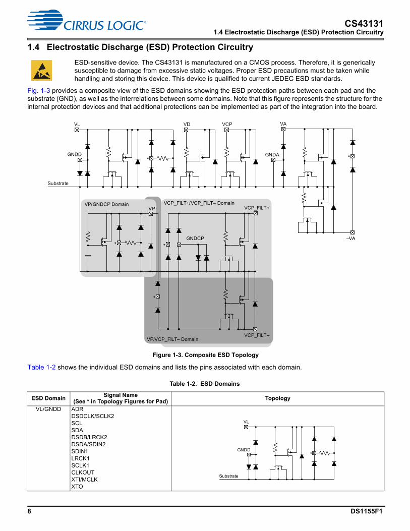
CS431311.4 Electrostatic Discharge (ESD) Protection Circuitry
1.4 Electrostatic Discharge (ESD) Protection Circuitry
Fig. 1-3 provides a composite view of the ESD domains showing the ESD protection paths between each pad and the substrate (GND), as well as the interrelations between some domains. Note that this figure represents the structure for the internal protection devices and that additional protections can be implemented as part of the integration into the board.
Figure 1-3. Composite ESD Topology
Table 1-2 shows the individual ESD domains and lists the pins associated with each domain.
ESD-sensitive device. The CS43131 is manufactured on a CMOS process. Therefore, it is generically susceptible to damage from excessive static voltages. Proper ESD precautions must be taken while handling and storing this device. This device is qualified to current JEDEC ESD standards.
Table 1-2. ESD Domains
ESD DomainSignal Name
(See * in Topology Figures for Pad)Topology
VL/GNDD ADRDSDCLK/SCLK2SCLSDADSDB/LRCK2DSDA/SDIN2SDIN1LRCK1SCLK1CLKOUTXTI/MCLKXTO
VL
GNDD
Substrate
VD VA
–VA
VP
*
*
VCP_FILT+
GNDCP
VCP_FILT–
*
*
VCP
GNDA
VP/GNDCP Domain
VP/VCP_FILT– Domain
VCP_FILT+/VCP_FILT– Domain
*
VL
GNDD
Substrate
*
DS1155F1 9
CS431311.4 Electrostatic Discharge (ESD) Protection Circuitry
VA/–VA FLYN_VAFLYP_VAFILT+FILT–
VP/GNDCP RESET
INTVP/VCP_FILT– FLYP_VCP
FLYC_VCPHP_DETECT
VCP_FILT+/VCP_FILT–
FLYN_VCPHPINAHPINBHPOUTAHPOUTBHPREFAHPREFB
Table 1-2. ESD Domains (Cont.)
ESD DomainSignal Name
(See * in Topology Figures for Pad)Topology
VA
–VA
GNDA
Substrate
*
VP
*
VCP_FILT+
GNDCP
VCP_FILT–
Substrate
*
*
VP/GNDCP Domain
VP/VCP_FILT– Domain
VCP_FILT+/VCP_FILT– Domain
10 DS1155F1
CS431312 Typical Connection Diagram
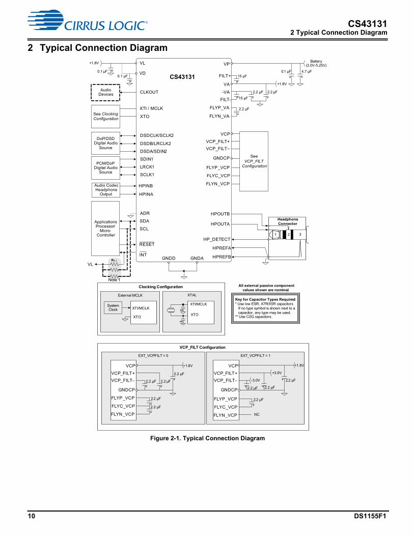
2 Typical Connection Diagram
Figure 2-1. Typical Connection Diagram
VCP_FILT Configuration
GNDD GNDA
VA
+1.8V VL
VCP_FILT+
FLYN_VA
FLYP_VA 2.2 µF
*
-VA
HPOUTA
HPOUTB
HPREFA
HP_DETECT
Headphone Connector
1 2 3
*
2.2 µF
HPINB
HPINA
Audio Codec Headphone
Output
0.1 µF
HPREFB
FLYN_VCP
FLYP_VCP
CLKOUTAudio Devices
XTI / MCLK
XTOSee ClockingConfiguration
FILT-
FILT+ 15 µF
*
GNDCP
VCP
Battery(3.0V-5.25V)
*
2.2 µFFLYC_VCP
VCP_FILT–
VP
+1.8V
2.2 µF
*
2.2 µF
*
*
4.7 µF
PCM/DoPDigital Audio
Source
RESET
Applications Processor/
Micro-Controller
INTRP_I
VL
ADR
SDA
SCL
VD0.1 µF
*
15 µF*
Clocking Configuration
External MCLK
System Clock XTI/MCLK
XTO
* 0.1 µF
*
EXT_VCPFILT = 1EXT_VCPFILT = 0
VCP_FILT+
GNDCP
VCP +1.8V
VCP_FILT– 2.2 µF
*
2.2 µF
*
2.2 µF
*
VCP_FILT+
GNDCP
VCP +1.8V
VCP_FILT–
2.2 µF* 2.2 µF*
2.2 µF*
+3.0V
-3.0V
See VCP_FILT
Configuration
*
2.2 µF
FLYN_VCP
FLYP_VCP
FLYC_VCP*
2.2 µF
FLYN_VCP
FLYP_VCP
*
2.2 µFFLYC_VCP
NC
XTAL
XTI/MCLK
XTO
SCLK1
LRCK1
SDIN1
DSDCLK/SCLK2
DSDB/LRCLK2
DSDA/SDIN2
**
**
All external passive component values shown are nominal.
Key for Capacitor Types Required:* Use low ESR, X7R/X5R capacitors
If no type symbol is shown next to a capacitor, any type may be used.
** Use C0G capacitors.
DoP/DSDDigital Audio
Source
Note 1
CS43131

DS1155F1 11
CS431312 Typical Connection Diagram
Figure 2-2. Typical Connection Diagram (Mono Mode)Note: 1. The value for RP_I can be determined by the interrupt pin specification in Table 3-13.
VCP_FILT Configuration
GNDD GNDA
VA
+1.8V VL
VCP_FILT+
FLYN_VA
FLYP_VA 2.2 µF
*
-VA
HPOUTA
HPOUTB
HPREFA
HP_DETECT
*
2.2 µF
HPINB
HPINA
Audio Codec Headphone
Output
0.1 µF
HPREFB
FLYN_VCP
FLYP_VCP
CLKOUTAudio Devices
XTI / MCLK
XTOSee ClockingConfiguration
FILT-
FILT+ 15 µF
*
GNDCP
VCP
Battery(3.0V-5.25V)
*
2.2 µFFLYC_VCP
VCP_FILT–
VP
+1.8V
2.2 µF
*
2.2 µF
*
*
4.7 µF
PCM/DoPDigital Audio
Source
RESET
Applications Processor/
Micro-Controller
INTRP_I
VL
ADR
SDA
SCL
VD0.1 µF
*
15 µF*
Clocking Configuration
External MCLK
System Clock XTI/MCLK
XTO
* 0.1 µF
*
EXT_VCPFILT = 1EXT_VCPFILT = 0
VCP_FILT+
GNDCP
VCP +1.8V
VCP_FILT– 2.2 µF
*
2.2 µF
*
2.2 µF
*
VCP_FILT+
GNDCP
VCP +1.8V
VCP_FILT–
2.2 µF* 2.2 µF*
2.2 µF*
+3.0V
-3.0V
See VCP_FILT
Configuration
*
2.2 µF
FLYN_VCP
FLYP_VCP
FLYC_VCP*
2.2 µF
FLYN_VCP
FLYP_VCP
*
2.2 µFFLYC_VCP
NC
XTAL
XTI/MCLK
XTO
SCLK1
LRCK1
SDIN1
DSDCLK/SCLK2
DSDB/LRCLK2
DSDA/SDIN2
**
**
All external passive component values shown are nominal.
Key for Capacitor Types Required:* Use low ESR, X7R/X5R capacitors If no type symbol is shown next to a capacitor, any type may be used.** Use C0G capacitors.
DoP/DSDDigital Audio
Source
XLR
2 3
1
Note 1
CS43131
12 DS1155F1
CS431313 Characteristics and Specifications
3 Characteristics and Specifications
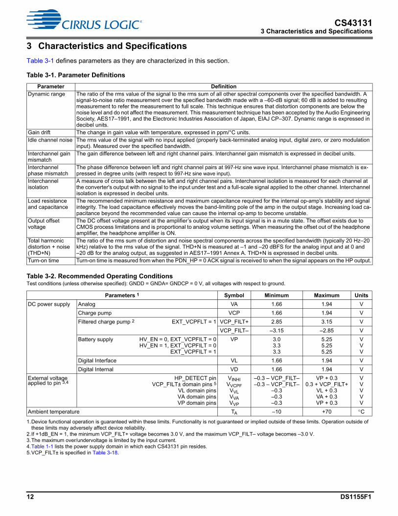
Table 3-1 defines parameters as they are characterized in this section.
Table 3-1. Parameter Definitions
Parameter DefinitionDynamic range The ratio of the rms value of the signal to the rms sum of all other spectral components over the specified bandwidth. A
signal-to-noise ratio measurement over the specified bandwidth made with a –60-dB signal; 60 dB is added to resulting measurement to refer the measurement to full scale. This technique ensures that distortion components are below the noise level and do not affect the measurement. This measurement technique has been accepted by the Audio Engineering Society, AES17–1991, and the Electronic Industries Association of Japan, EIAJ CP–307. Dynamic range is expressed in decibel units.
Gain drift The change in gain value with temperature, expressed in ppm/°C units.Idle channel noise The rms value of the signal with no input applied (properly back-terminated analog input, digital zero, or zero modulation
input). Measured over the specified bandwidth.Interchannel gain mismatch
The gain difference between left and right channel pairs. Interchannel gain mismatch is expressed in decibel units.
Interchannel phase mismatch
The phase difference between left and right channel pairs at 997-Hz sine wave input. Interchannel phase mismatch is ex-pressed in degree units (with respect to 997-Hz sine wave input).
Interchannel isolation
A measure of cross talk between the left and right channel pairs. Interchannel isolation is measured for each channel at the converter's output with no signal to the input under test and a full-scale signal applied to the other channel. Interchannel isolation is expressed in decibel units.
Load resistance and capacitance
The recommended minimum resistance and maximum capacitance required for the internal op-amp's stability and signal integrity. The load capacitance effectively moves the band-limiting pole of the amp in the output stage. Increasing load ca-pacitance beyond the recommended value can cause the internal op-amp to become unstable.
Output offset voltage
The DC offset voltage present at the amplifier’s output when its input signal is in a mute state. The offset exists due to CMOS process limitations and is proportional to analog volume settings. When measuring the offset out of the headphone amplifier, the headphone amplifier is ON.
Total harmonic distortion + noise (THD+N)
The ratio of the rms sum of distortion and noise spectral components across the specified bandwidth (typically 20 Hz–20 kHz) relative to the rms value of the signal. THD+N is measured at –1 and –20 dBFS for the analog input and at 0 and –20 dB for the analog output, as suggested in AES17–1991 Annex A. THD+N is expressed in decibel units.
Turn-on time Turn-on time is measured from when the PDN_HP = 0 ACK signal is received to when the signal appears on the HP output.
Table 3-2. Recommended Operating ConditionsTest conditions (unless otherwise specified): GNDD = GNDA= GNDCP = 0 V, all voltages with respect to ground.
Parameters 1
1.Device functional operation is guaranteed within these limits. Functionality is not guaranteed or implied outside of these limits. Operation outside of these limits may adversely affect device reliability.
Symbol Minimum Maximum Units
DC power supply Analog VA 1.66 1.94 V
Charge pump VCP 1.66 1.94 V
Filtered charge pump 2
2.If +1dB_EN = 1, the minimum VCP_FILT+ voltage becomes 3.0 V, and the maximum VCP_FILT– voltage becomes –3.0 V.
EXT_VCPFLT = 1 VCP_FILT+ 2.85 3.15 V
VCP_FILT– –3.15 –2.85 V
Battery supply HV_EN = 0, EXT_VCPFILT = 0HV_EN = 1, EXT_VCPFILT = 0
EXT_VCPFILT = 1
VP 3.03.33.3
5.255.255.25
VVV
Digital Interface VL 1.66 1.94 V
Digital Internal VD 1.66 1.94 V
External voltage applied to pin 3,4
3.The maximum over/undervoltage is limited by the input current.4.Table 1-1 lists the power supply domain in which each CS43131 pin resides.
HP_DETECT pinVCP_FILT± domain pins 5
VL domain pinsVA domain pinsVP domain pins
5.VCP_FILT± is specified in Table 3-18.
VINHIVVCPF
VVLVVAVVP
–0.3 – VCP_FILT––0.3 – VCP_FILT–
–0.3–0.3–0.3
VP + 0.30.3 + VCP_FILT+
VL + 0.3VA + 0.3VP + 0.3
VVVVV
Ambient temperature TA –10 +70 C
DS1155F1 13
CS431313 Characteristics and Specifications
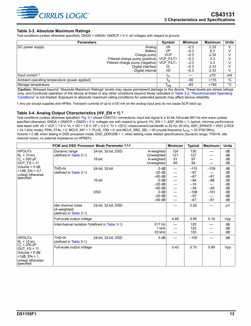
Table 3-3. Absolute Maximum RatingsTest conditions (unless otherwise specified): GNDD = GNDA= GNDCP = 0 V; all voltages with respect to ground.
Parameters Symbol Minimum Maximum UnitsDC power supply Analog
BatteryCharge pump
Filtered charge pump (positive)Filtered charge pump (negative)
Digital interfaceDigital internal
VAVP
VCPVCP_FILT+VCP_FILT–
VLVD
–0.3–0.3–0.3–0.3–3.3–0.3–0.3
2.336.32.333.30.32.332.33
VVVVVVV
Input current 1
1.Any pin except supplies and HPINx. Transient currents of up to ±100 mA on the analog input pins do not cause SCR latch-up.
Iin — ±10 mAAmbient operating temperature (power applied) TA –50 +115 °CStorage temperature Tstg –65 +150 °CCaution: Stresses beyond “Absolute Maximum Ratings” levels may cause permanent damage to the device. These levels are stress ratings only, and functional operation of the device at these or any other conditions beyond those indicated in Table 3-2, “Recommended Operating Conditions” is not implied. Exposure to absolute maximum rating conditions for extended periods may affect device reliability.
Table 3-4. Analog Output Characteristics (HV_EN = 1) 1Test conditions (unless otherwise specified): Fig. 2-1 shows CS43131 connections; input test signal is a 32-bit, full-scale 997-Hz sine wave (unless specified otherwise); GNDA = GNDCP = GNDD = 0 V; voltages are with respect to ground; HV_EN = 1; ASP_M/Sb = 1; typical, min/max performance data taken with VA = VCP = 1.8 V; VL = VD = 1.8 V; VP = 3.6 V; TA = +25°C; measurement bandwidth is 20 Hz–20 kHz; ASP_SPRATE = 0001 (LRCK = 44.1-kHz mode); PDN_XTAL = 0, MCLK_INT = 1, PLUS_1DB = 0, and MCLK_SRC_SEL = 00 (crystal frequency fXTAL = 22.5792 MHz); Volume = 0 dB; when testing in DSD processor mode, DSD_ZERODB = 1; when testing noise related specifications (dynamic range, THD+N, idle channel noise), no external impedance on HPREFx.
PCM and DSD Processor Mode Parameter 2,3,4 Minimum Typical Maximum Units
HPOUTxRL = 10 kCL = 200 pFOUT_FS = 11Volume = 0 dB+1dB_EN = 0,5unless otherwise specified
Dynamic range(defined in Table 3-1)
24-bit, 32-bit, DSD
16-bit
A-weightedUnweightedA-weightedUnweighted
1241219188
1301279794
————
dBdBdBdB
THD+N(defined in Table 3-1)
24-bit, 32-bit
16-bit
DSD
0 dB–20 dB–60 dB
0 dB–20 dB–60 dB
0 dB–20 dB–60 dB
—————————
–115–97–67–94–74–34
–108–97–67
–109—
–61–88—
–28–101
—–61
dBdBdBdBdBdBdBdBdB
Idle channel noise(A-weighted)(defined in Table 3-1)
24-bit, 32-bit, DSD — 0.55 — µV
Full-scale output voltage 4.66 4.90 5.14 Vpp
Interchannel isolation 6(defined in Table 3-1) 217 Hz1 kHz
20 kHz
———
120120100
———
dBdBdB
HPOUTxRL = 10 kCL = 200 pFOUT_FS = 11Volume = 0 dB+1dB_EN = 1,unless otherwise specified
THD+N(defined in Table 3-1)
24-bit, 32-bit, DSD 0 dB — –105 — dB
Full-scale output voltage 5.42 5.70 5.99 Vpp
14 DS1155F1
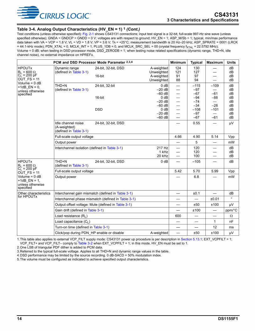
CS431313 Characteristics and Specifications
HPOUTxRL = 600 CL = 200 pFOUT_FS = 11Volume = 0 dB+1dB_EN = 0,unless otherwise specified
Dynamic range(defined in Table 3-1)
24-bit, 32-bit, DSD
16-bit
A-weightedUnweightedA-weightedUnweighted
1241219188
1301279794
————
dBdBdBdB
THD+N(defined in Table 3-1)
24-bit, 32-bit
16-bit
DSD
0 dB–20 dB–60 dB
0 dB–20 dB–60 dB
0 dB–20 dB–60 dB
—————————
–115–97–67–94–74–34
–108–97–67
–109—
–61–88—
–28–101
—–61
dBdBdBdBdBdBdBdBdB
Idle channel noise(A-weighted)(defined in Table 3-1)
24-bit, 32-bit, DSD — 0.55 — µV
Full-scale output voltage 4.66 4.90 5.14 Vpp
Output power — 5 — mW
Interchannel isolation (defined in Table 3-1) 217 Hz1 kHz
20 kHz
———
120120100
———
dBdBdB
HPOUTxRL = 600 CL = 200 pFOUT_FS = 11Volume = 0 dB+1dB_EN = 1,unless otherwise specified
THD+N(defined in Table 3-1)
24-bit, 32-bit, DSD 0 dB — –105 — dB
Full-scale output voltage 5.42 5.70 5.99 Vpp
Output power — 6.8 — mW
Other characteristics for HPOUTx
Interchannel gain mismatch (defined in Table 3-1) — ±0.1 — dB
Interchannel phase mismatch (defined in Table 3-1) — — ±0.01 °
Output offset voltage: Mute (defined in Table 3-1) — ±50 ±100 µV
Gain drift (defined in Table 3-1) — ±100 — ppm/°C
Load resistance (RL) 600 — —
Load capacitance (CL) — — 1 nF
Turn-on time (defined in Table 3-1) — — 12 ms
Click/pop during PDN_HP enable or disable A-weighted — ±50 ±100 µV
1.This table also applies to external VCP_FILT supply mode: CS43131 power up procedure is per description in Section 5.13.1; EXT_VCPFILT = 1; VCP_FILT+ and VCP_FILT– comply to Table 3-2 when EXT_VCPFILT = 1; in this mode, HV_EN must be set to 1.
2.One LSB of triangular PDF dither is added to PCM data.3.Referred to the typical full-scale voltage. Applies to all THD+N and dynamic range values in the table.4.DSD performance may be limited by the source recording. 0 dB-SACD = 50% modulation index. 5.The volume must be configured as indicated to achieve specified output characteristics.
Table 3-4. Analog Output Characteristics (HV_EN = 1) 1 (Cont.)Test conditions (unless otherwise specified): Fig. 2-1 shows CS43131 connections; input test signal is a 32-bit, full-scale 997-Hz sine wave (unless specified otherwise); GNDA = GNDCP = GNDD = 0 V; voltages are with respect to ground; HV_EN = 1; ASP_M/Sb = 1; typical, min/max performance data taken with VA = VCP = 1.8 V; VL = VD = 1.8 V; VP = 3.6 V; TA = +25°C; measurement bandwidth is 20 Hz–20 kHz; ASP_SPRATE = 0001 (LRCK = 44.1-kHz mode); PDN_XTAL = 0, MCLK_INT = 1, PLUS_1DB = 0, and MCLK_SRC_SEL = 00 (crystal frequency fXTAL = 22.5792 MHz); Volume = 0 dB; when testing in DSD processor mode, DSD_ZERODB = 1; when testing noise related specifications (dynamic range, THD+N, idle channel noise), no external impedance on HPREFx.
PCM and DSD Processor Mode Parameter 2,3,4 Minimum Typical Maximum Units
DS1155F1 15
CS431313 Characteristics and Specifications
6.Output test configuration. Symbolized component values are specified in the test conditions.
Table 3-5. Analog Output Characteristics (HV_EN = 0) 1Test conditions (unless otherwise specified): Fig. 2-1 shows CS43131 connections; input test signal is a 32-bit, full-scale 997-Hz sine wave (unless specified otherwise); GNDA = GNDCP = GNDD = 0 V; voltages are with respect to ground; HV_EN = 0; ASP_M/Sb = 1; typical, min/max performance data taken with VA = VCP = 1.8 V; VL = VD = 1.8 V; VP = 3.6 V; TA = +25°C; measurement bandwidth is 20 Hz–20 kHz; ASP_SPRATE = 0001 (LRCK = 44.1-kHz mode); PDN_XTAL = 0, MCLK_INT = 1, and MCLK_SRC_SEL = 00 (crystal frequency fXTAL = 22.5792 MHz); Volume = 0 dB; when testing in DSD processor mode, DSD_ZERODB = 1; when testing noise related specifications (dynamic range, THD+N, idle channel noise), no external impedance on HPREFx.
PCM and DSD Processor Mode Parameter 2,3,4 Minimum Typical Maximum Units
HPOUTx;RL = 10 kCL = 200 pFOUT_FS = 10Volume = 0 dB,5unless otherwise specified
Dynamic range(defined in Table 3-1)
24-bit, 32-bit, DSD
16-bit
A-weightedUnweightedA-weightedUnweighted
1221199188
1281259794
————
dBdBdBdB
THD+N (defined in Table 3-1)
24-bit, 32-bit
16-bit
DSD
0 dB–20 dB–60 dB
0 dB–20 dB–60 dB
0 dB–20 dB–60 dB
—————————
–113–95–65–94–74–34–109–95–65
–107—
–59–88—
–28–103
—–59
dBdBdBdBdBdBdBdBdB
Idle channel noise(A-weighted)(defined in Table 3-1)
24-bit, 32-bit, DSD — 0.55 — µV
Full-scale output voltage 3.76 3.96 4.16 Vpp
Interchannel isolation 6 (defined in Table 3-1) 217 Hz1 kHz
20 kHz
———
120120100
———
dBdBdB
HPOUTx; RL = 600 CL = 200 pFOUT_FS = 10Volume = 0 dB,unless otherwise specified
Dynamic range(defined in Table 3-1)
24-bit, 32-bit, DSD
16-bit
A-weightedUnweightedA-weightedUnweighted
1221199188
1281259794
————
dBdBdBdB
THD+N(defined in Table 3-1)
24-bit, 32-bit
16-bit
DSD
0 dB–20 dB–60 dB
0 dB–20 dB–60 dB
0 dB–20 dB–60 dB
—————————
–113–95–65–94–74–34–109–95–65
–107—
–59–88—
–28–103
—–59
dBdBdBdBdBdBdBdBdB
Idle channel noise(A-weighted)(defined in Table 3-1)
24-bit, 32-bit, DSD — 0.55 — µV
Full-scale output voltage 3.76 3.96 4.16 Vpp
Output power — 3.3 — mW
Interchannel isolation 6 (defined in Table 3-1) 217 Hz1 kHz
20 kHz
———
120120100
———
dBdBdB
Test LoadHPOUTA CLA
HPREFA
RLA
Measurement Device
–
+
–
+HPOUTB
HPREFB
CH1
CH2
CLB RLB
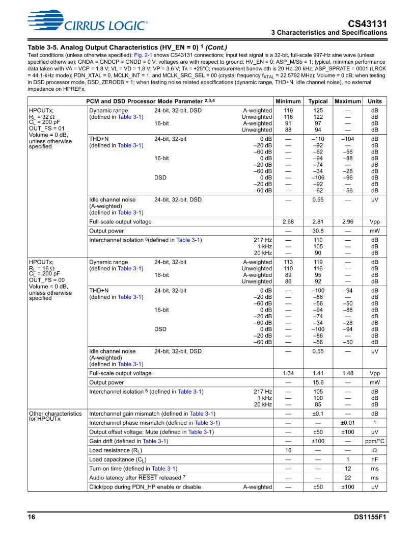
16 DS1155F1
CS431313 Characteristics and Specifications
HPOUTx; RL = 32 CL = 200 pFOUT_FS = 01Volume = 0 dB,unless otherwise specified
Dynamic range(defined in Table 3-1)
24-bit, 32-bit, DSD
16-bit
A-weightedUnweightedA-weightedUnweighted
1191169188
1251229794
————
dBdBdBdB
THD+N(defined in Table 3-1)
24-bit, 32-bit
16-bit
DSD
0 dB–20 dB–60 dB
0 dB–20 dB–60 dB
0 dB–20 dB–60 dB
—————————
–110–92–62–94–74–34–106–92–62
–104—
–56–88—
–28–96—
–56
dBdBdBdBdBdBdBdBdB
Idle channel noise(A-weighted)(defined in Table 3-1)
24-bit, 32-bit, DSD — 0.55 — µV
Full-scale output voltage 2.68 2.81 2.96 Vpp
Output power — 30.8 — mW
Interchannel isolation 6(defined in Table 3-1) 217 Hz1 kHz
20 kHz
———
11010590
———
dBdBdB
HPOUTx; RL = 16 CL = 200 pFOUT_FS = 00Volume = 0 dB,unless otherwise specified
Dynamic range(defined in Table 3-1)
24-bit, 32-bit
16-bit
A-weightedUnweightedA-weightedUnweighted
1131108986
1191169592
————
dBdBdBdB
THD+N(defined in Table 3-1)
24-bit, 32-bit
16-bit
DSD
0 dB–20 dB–60 dB
0 dB–20 dB–60 dB
0 dB–20 dB–60 dB
—————————
–100–86–56–94–74–34–100–86–56
–94—
–50–88—
–28–94—
–50
dBdBdBdBdBdBdBdBdB
Idle channel noise(A-weighted)(defined in Table 3-1)
24-bit, 32-bit, DSD — 0.55 — µV
Full-scale output voltage 1.34 1.41 1.48 Vpp
Output power — 15.6 — mW
Interchannel isolation 6 (defined in Table 3-1) 217 Hz1 kHz
20 kHz
———
10510085
———
dBdBdB
Other characteristics for HPOUTx
Interchannel gain mismatch (defined in Table 3-1) — ±0.1 — dB
Interchannel phase mismatch (defined in Table 3-1) — — ±0.01 °
Output offset voltage: Mute (defined in Table 3-1) — ±50 ±100 µV
Gain drift (defined in Table 3-1) — ±100 — ppm/°C
Load resistance (RL) 16 — —
Load capacitance (CL) — — 1 nF
Turn-on time (defined in Table 3-1) — — 12 ms
Audio latency after RESET released 7 — — 22 ms
Click/pop during PDN_HP enable or disable A-weighted — ±50 ±100 µV
Table 3-5. Analog Output Characteristics (HV_EN = 0) 1 (Cont.)Test conditions (unless otherwise specified): Fig. 2-1 shows CS43131 connections; input test signal is a 32-bit, full-scale 997-Hz sine wave (unless specified otherwise); GNDA = GNDCP = GNDD = 0 V; voltages are with respect to ground; HV_EN = 0; ASP_M/Sb = 1; typical, min/max performance data taken with VA = VCP = 1.8 V; VL = VD = 1.8 V; VP = 3.6 V; TA = +25°C; measurement bandwidth is 20 Hz–20 kHz; ASP_SPRATE = 0001 (LRCK = 44.1-kHz mode); PDN_XTAL = 0, MCLK_INT = 1, and MCLK_SRC_SEL = 00 (crystal frequency fXTAL = 22.5792 MHz); Volume = 0 dB; when testing in DSD processor mode, DSD_ZERODB = 1; when testing noise related specifications (dynamic range, THD+N, idle channel noise), no external impedance on HPREFx.
PCM and DSD Processor Mode Parameter 2,3,4 Minimum Typical Maximum Units
DS1155F1 17
CS431313 Characteristics and Specifications
1.This table also applies to external VCP_FILT supply mode: CS43131 power up procedure as described in Section 4.3.5; EXT_VCPFILT=1; VCP_FILT+ and VCP_FILT– comply to Table 3-2 when EXT_VCPFILT = 1; in this mode, HV_EN must be set to 1.
2.One LSB of triangular PDF dither is added to PCM data.3.Referred to the typical full-scale voltage. Applies to all THD+N and dynamic range values in the table.4.DSD performance may be limited by the source recording. 0 dB-SACD = 50% modulation index. 5.The volume must be configured as indicated to achieve specified output characteristics.6.HP output test configuration. Symbolized component values are specified in the test
conditions.
7.With I2C normal speed mode and 22.5792-MHz XTAL used as MCLK source, this specification is measured from reset released to when the audio signal appears on the output per power-up sequence listed in Section 5.13.1. PCM_SZC should be set to Immediate (PCM_SZC = 00) to hear audio at 20 ms after startup.
Table 3-6. Wideband Flatness Mode Analog Output Characteristics 1Test conditions (unless otherwise specified): Fig. 2-1 shows CS43131 connections; input test signal is a 32-bit, full-scale 997-Hz sine wave (unless specified otherwise); GNDA = GNDCP = GNDD = 0 V; voltages are with respect to ground; ASP_M/Sb = 1; typical, min/max performance data taken with VA = VCP = 1.8 V; VL = VD = 1.8 V; VP = 3.6 V; TA = +25°C; measurement bandwidth is 20 Hz–90 kHz; ASP_SPRATE = 0110 (LRCK = 192-kHz mode); PDN_XTAL = 0, MCLK_INT = 1, and MCLK_SRC_SEL = 00 (crystal frequency fXTAL = 22.5792 MHz); Volume = 0 dB; when testing noise related specifications (dynamic range, THD+N, idle channel noise), no external impedance on HPREFx.
Wideband Flatness Mode Parameter 2,3 Minimum Typical Maximum Units
HPOUTxRL = 600 CL = 200 pFOUT_FS = 11Volume = 0 dB+1dB_EN = 0HV_EN = 1,unless otherwise specified
Dynamic range(defined in Table 3-1)
24-bit, 32-bit A-weighted 122 128 — dB
THD+N (20 Hz–20 kHz,defined in Table 3-1)
24-bit, 32-bit 0 dB–20 dB–60 dB
———
–112–97–67
–106—
–61
dBdBdB
Idle channel noise(A-weighted)(defined in Table 3-1)
24-bit, 32-bit — 0.69 — µV
Full-scale output voltage 4.66 4.90 5.14 Vpp
Output power — 5 — mW
Interchannel isolation (defined in Table 3-1) 217 Hz1 kHz
20 kHz
———
120120110
———
dBdBdB
HPOUTxRL = 600 CL = 200 pFOUT_FS = 11Volume = 0 dB+1dB_EN = 1HV_EN = 1,unless otherwise specified
THD+N (20 Hz–20 kHz,defined in Table 3-1)
24-bit, 32-bit 0 dB — –105 –99 dB
Full-scale output voltage 5.42 5.7 5.99 Vpp
Output power — 6.8 — mW
Test LoadHPOUTA CLA
HPREFA
RLA
Measurement Device
–
+
–
+HPOUTB
HPREFB
CH1
CH2
CLB RLB
18 DS1155F1
CS431313 Characteristics and Specifications
HPOUTx; RL = 32 CL = 200 pFOUT_FS = 01Volume = 0 dBHV_EN = 0,unless otherwise specified
Dynamic range(defined in Table 3-1)
24-bit, 32-bit A-weighted 117 123 — dB
Dynamic range(MCLK = 19.2 MHz,MCLK_SRC_SEL = 01,MCLK_INT = 1)
24-bit, 32-bit (DRE_EN = 1)
24-bit, 32-bit (DRE_EN = 0)
A-weightedUnweightedA-weightedUnweighted
115889464
1219410070
————
dBdBdBdB
THD+N (20 Hz–20 kHz,defined in Table 3-1)
24-bit, 32-bit 0 dB–20 dB–60 dB
———
–110–92–62
–104—
–56
dBdBdB
THD+N (20 Hz–90 kHz,defined in Table 3-1)
24-bit, 32-bit 0 dB–20 dB–60 dB
———
–89–78–38
–83—
–32
dBdBdB
Idle channel noise(A-weighted)(defined in Table 3-1)
24-bit, 32-bit — 0.69 — µV
Full-scale output voltage 2.68 2.81 2.96 Vpp
Output power — 30.8 — mW
Interchannel isolation 4 (defined in Table 3-1) 217 Hz1 kHz
20 kHz
———
11010590
———
dBdBdB
Other characteristics for HPOUTx
Interchannel gain mismatch (defined in Table 3-1) — ±0.1 — dB
Interchannel phase mismatch (defined in Table 3-1) — — ±0.01 °
Output offset voltage: Mute (defined in Table 3-1) — ±50 ±100 µV
Gain drift (defined in Table 3-1) — ±100 — ppm/°C
Load resistance (RL) 6 — —
Load capacitance (CL) — — 1 nF
Turn-on time (defined in Table 3-1) — — 12 ms
Click/pop during PDN_HP enable or disable A-weighted — ±50 ±100 µV
1.This table also applies to external VCP_FILT supply mode: CS43131 power up procedure is per description in Section 5.13.1; EXT_VCPFILT = 1; VCP_FILT+ and VCP_FILT– comply to Table 3-2 when EXT_VCPFILT = 1; in this mode, HV_EN must be set to 1.
2.One LSB of triangular PDF dither is added to PCM data.3.Referred to the typical full-scale voltage. Applies to all THD+N and dynamic range values in the table.4.HP output test configuration. Symbolized component values are specified in the test
conditions.
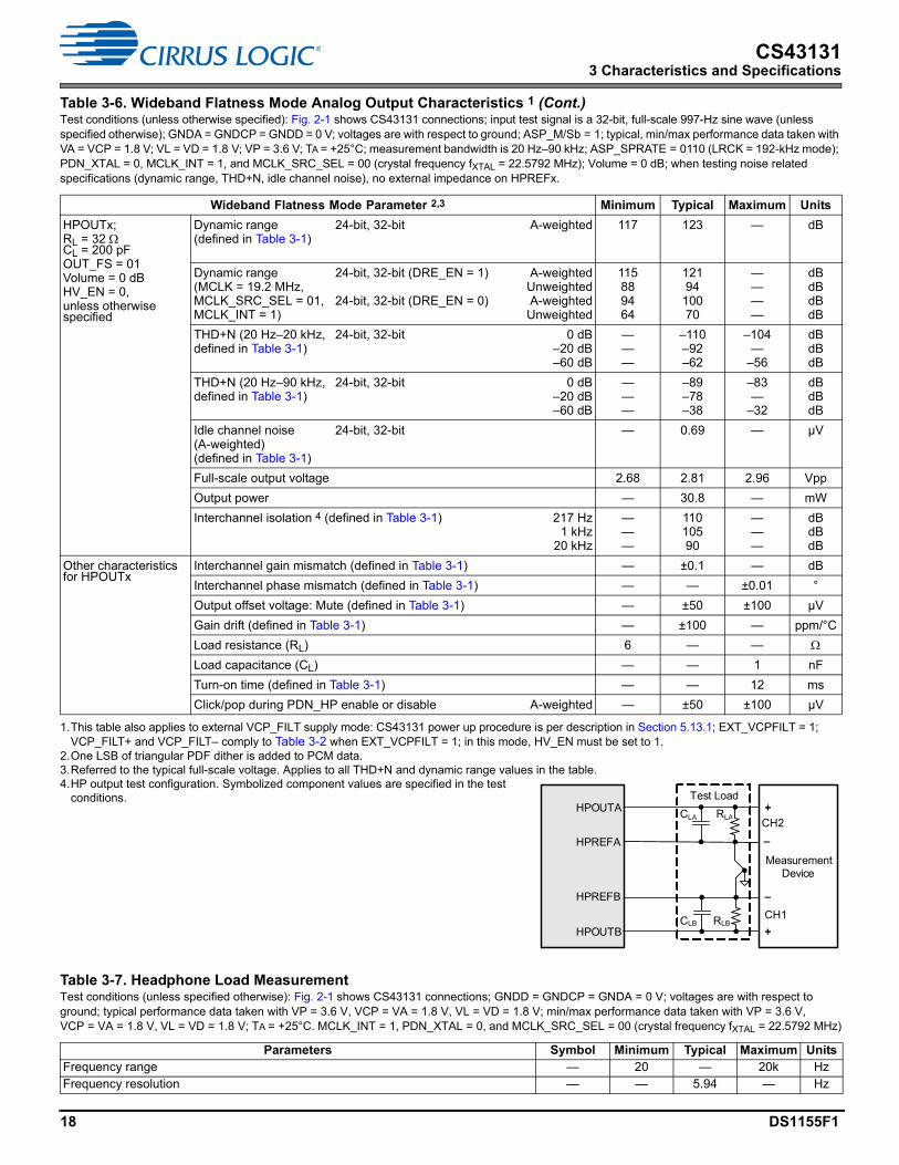
Table 3-7. Headphone Load MeasurementTest conditions (unless specified otherwise): Fig. 2-1 shows CS43131 connections; GNDD = GNDCP = GNDA = 0 V; voltages are with respect to ground; typical performance data taken with VP = 3.6 V, VCP = VA = 1.8 V, VL = VD = 1.8 V; min/max performance data taken with VP = 3.6 V, VCP = VA = 1.8 V, VL = VD = 1.8 V; TA = +25°C. MCLK_INT = 1, PDN_XTAL = 0, and MCLK_SRC_SEL = 00 (crystal frequency fXTAL = 22.5792 MHz)
Parameters Symbol Minimum Typical Maximum UnitsFrequency range — 20 — 20k HzFrequency resolution — — 5.94 — Hz
Table 3-6. Wideband Flatness Mode Analog Output Characteristics 1 (Cont.)Test conditions (unless otherwise specified): Fig. 2-1 shows CS43131 connections; input test signal is a 32-bit, full-scale 997-Hz sine wave (unless specified otherwise); GNDA = GNDCP = GNDD = 0 V; voltages are with respect to ground; ASP_M/Sb = 1; typical, min/max performance data taken with VA = VCP = 1.8 V; VL = VD = 1.8 V; VP = 3.6 V; TA = +25°C; measurement bandwidth is 20 Hz–90 kHz; ASP_SPRATE = 0110 (LRCK = 192-kHz mode); PDN_XTAL = 0, MCLK_INT = 1, and MCLK_SRC_SEL = 00 (crystal frequency fXTAL = 22.5792 MHz); Volume = 0 dB; when testing noise related specifications (dynamic range, THD+N, idle channel noise), no external impedance on HPREFx.
Wideband Flatness Mode Parameter 2,3 Minimum Typical Maximum Units
Test LoadHPOUTA CLA
HPREFA
RLA
Measurement Device
–
+
–
+HPOUTB
HPREFB
CH1
CH2
CLB RLB

DS1155F1 19
CS431313 Characteristics and Specifications
Low frequency impedance range — 8 — 1200 Relative impedance measurement capability 1 — –12 2 — +12 dBImpedance measurement accuracy 3 Gain error
Offset——
–10–1
——
+101
%
1.Impedance measurement range is relative to low-frequency HP load impedance measured.2.Or 4 , whichever is greater.3.Accuracy is referred to reported impedance.
Table 3-8. Alternate Headphone PathTest conditions (unless specified otherwise): Fig. 2-1 shows CS43131 connections; GNDD = GNDCP = GNDA = 0 V; voltages are with respect to ground; typical performance data taken with VP = 3.6 V, VCP = VA = 1.8 V, VL = VD = 1.8 V; min/max performance data taken with VP = 3.6 V, VCP = 1.8 V, VA = 0 V, VL = VD = 1.8 V; RL = 32 ; TA = +25°C; measurement bandwidth is 20 Hz–20 kHz; MCLK_SRC_SEL = 10, PDN_XTAL = 1.
Parameters Symbol Minimum Typical Maximum UnitsSwitch on characteristics(PDN_HP = 1HP_IN_EN = 1)
Signal range when switch on 1
1.When switch is on, maximally allowable voltage applied to HPINx pins.
VINAI — — 3.00 VppTHD+N with 32 @ 2.82 Vpp — — –103 — dBInterchannel isolation 217 Hz
1 kHz20 kHz
— 104——
11010590
———
dBdBdB
HPINx turn-on time 2
2.HPINx turn-on time is measured when setting HP_IN_EN = 1. I2C ACK signal is received to when the signal appears on the HP out. MCLK_SRC_SEL = 00, PDN_XTAL = 0, MCLK_INT = 1. For EXT_VCPFILT = 1, VCP_FILT± has been properly charged to expected nominal values.
EXT_VCPFILT = 1EXT_VCPFILT = 0
tHPIN_ON ——
——
801.1
sms
Switch off characteristics(PDN_HP = 1,HP_IN_EN = 0)
Analog signal range when switched off 3,4
3.When switch is off, maximally allowable voltage applied to HPINx pins.4.Before switch off event, it is required HPINx signal is within this range before the switch is turned off. When the switch is in off state, HPINx signal
cannot exceed this specified range.
VINOFF — — 0.3 VpTurn-off time 5
5.HPINx turn-off time is measured when HP_IN_EN = 0 ACK signal is received to when the signal disappears from the HP out. This spec also applies when register settings are: MCLK_SRC_SEL = 00, PDN_XTAL = 0, MCLK_INT = 1.
tHPIN_OFF — — 20 sOff isolation 6
6.Off isolation specification is measured with VINOFF = 0.1 Vp input.
217 Hz1 kHz
20 kHz
———
120120100
———
dBdBdB
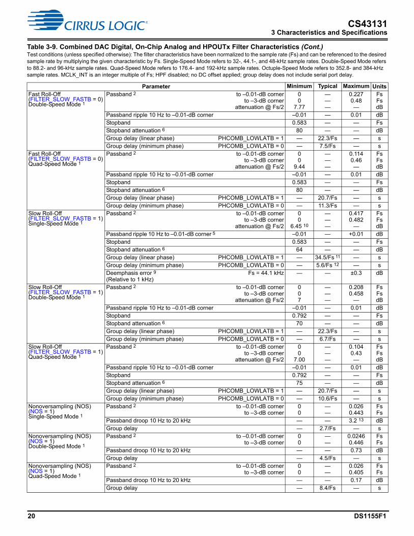
Table 3-9. Combined DAC Digital, On-Chip Analog and HPOUTx Filter CharacteristicsTest conditions (unless specified otherwise): The filter characteristics have been normalized to the sample rate (Fs) and can be referenced to the desired sample rate by multiplying the given characteristic by Fs. Single-Speed Mode refers to 32-, 44.1-, and 48-kHz sample rates. Double-Speed Mode refers to 88.2- and 96-kHz sample rates. Quad-Speed Mode refers to 176.4- and 192-kHz sample rates. Octuple-Speed Mode refers to 352.8- and 384-kHz sample rates. MCLK_INT is an integer multiple of Fs; HPF disabled; no DC offset applied; group delay does not include serial port delay.
Parameter Minimum Typical Maximum UnitsFast Roll-Off(FILTER_SLOW_FASTB = 0)Single-Speed Mode 1
Passband 2 to –0.01-dB cornerto –3-dB corner
attenuation @ Fs/2
00
8.44 3
———
0.4535 40.482
—
FsFsdB
Passband ripple 10 Hz to –0.01-dB corner 5 –0.01 — +0.01 dBStopband 0.547 — — FsStopband attenuation 6 110 — — dBGroup delay (linear phase) PHCOMP_LOWLATB = 1 — 39.5/Fs 7 — sGroup delay (minimum phase) PHCOMB_LOWLATB = 0 — 6.3/Fs 8 — sDeemphasis error 9(Relative to 1 kHz)
Fs = 44.1 kHz — — ±0.3 dB
Table 3-7. Headphone Load Measurement (Cont.)Test conditions (unless specified otherwise): Fig. 2-1 shows CS43131 connections; GNDD = GNDCP = GNDA = 0 V; voltages are with respect to ground; typical performance data taken with VP = 3.6 V, VCP = VA = 1.8 V, VL = VD = 1.8 V; min/max performance data taken with VP = 3.6 V, VCP = VA = 1.8 V, VL = VD = 1.8 V; TA = +25°C. MCLK_INT = 1, PDN_XTAL = 0, and MCLK_SRC_SEL = 00 (crystal frequency fXTAL = 22.5792 MHz)
Parameters Symbol Minimum Typical Maximum Units
20 DS1155F1
CS431313 Characteristics and Specifications
Fast Roll-Off(FILTER_SLOW_FASTB = 0)Double-Speed Mode 1
Passband 2 to –0.01-dB cornerto –3-dB corner
attenuation @ Fs/2
00
7.77
———
0.2270.48—
FsFsdB
Passband ripple 10 Hz to –0.01-dB corner –0.01 — 0.01 dBStopband 0.583 — — FsStopband attenuation 6 80 — — dBGroup delay (linear phase) PHCOMB_LOWLATB = 1 — 22.3/Fs — sGroup delay (minimum phase) PHCOMB_LOWLATB = 0 — 7.5/Fs — s
Fast Roll-Off(FILTER_SLOW_FASTB = 0)Quad-Speed Mode 1
Passband 2 to –0.01-dB cornerto –3-dB corner
attenuation @ Fs/2
00
9.44
———
0.1140.46—
FsFsdB
Passband ripple 10 Hz to –0.01-dB corner –0.01 — 0.01 dBStopband 0.583 — — FsStopband attenuation 6 80 — — dBGroup delay (linear phase) PHCOMB_LOWLATB = 1 — 20.7/Fs — sGroup delay (minimum phase) PHCOMB_LOWLATB = 0 — 11.3/Fs — s
Slow Roll-Off(FILTER_SLOW_FASTB = 1)Single-Speed Mode 1
Passband 2 to –0.01-dB cornerto –3-dB corner
attenuation @ Fs/2
00
6.45 10
———
0.4170.482
—
FsFsdB
Passband ripple 10 Hz to –0.01-dB corner 5 –0.01 — +0.01 dBStopband 0.583 — — FsStopband attenuation 6 64 — — dBGroup delay (linear phase) PHCOMB_LOWLATB = 1 — 34.5/Fs 11 — sGroup delay (minimum phase) PHCOMB_LOWLATB = 0 — 5.6/Fs 12 — sDeemphasis error 9(Relative to 1 kHz)
Fs = 44.1 kHz — — ±0.3 dB
Slow Roll-Off(FILTER_SLOW_FASTB = 1)Double-Speed Mode 1
Passband 2 to –0.01-dB cornerto –3-dB corner
attenuation @ Fs/2
007
———
0.2080.458
—
FsFsdB
Passband ripple 10 Hz to –0.01-dB corner –0.01 — 0.01 dBStopband 0.792 — — FsStopband attenuation 6 70 — — dBGroup delay (linear phase) PHCOMB_LOWLATB = 1 — 22.3/Fs — sGroup delay (minimum phase) PHCOMB_LOWLATB = 0 — 6.7/Fs — s
Slow Roll-Off(FILTER_SLOW_FASTB = 1)Quad-Speed Mode 1
Passband 2 to –0.01-dB cornerto –3-dB corner
attenuation @ Fs/2
00
7.00
———
0.1040.43—
FsFsdB
Passband ripple 10 Hz to –0.01-dB corner –0.01 — 0.01 dBStopband 0.792 — — FsStopband attenuation 6 75 — — dBGroup delay (linear phase) PHCOMB_LOWLATB = 1 — 20.7/Fs — sGroup delay (minimum phase) PHCOMB_LOWLATB = 0 — 10.6/Fs — s
Nonoversampling (NOS)(NOS = 1)Single-Speed Mode 1
Passband 2 to –0.01-dB cornerto –3-dB corner
00
——
0.0260.443
FsFs
Passband droop 10 Hz to 20 kHz — — 3.2 13 dBGroup delay — 2.7/Fs — s
Nonoversampling (NOS)(NOS = 1)Double-Speed Mode 1
Passband 2 to –0.01-dB cornerto –3-dB corner
00
——
0.02460.446
FsFs
Passband droop 10 Hz to 20 kHz — — 0.73 dBGroup delay — 4.5/Fs — s
Nonoversampling (NOS)(NOS = 1)Quad-Speed Mode 1
Passband 2 to –0.01-dB cornerto –3-dB corner
00
——
0.0260.405
FsFs
Passband droop 10 Hz to 20 kHz — — 0.17 dBGroup delay — 8.4/Fs — s
Table 3-9. Combined DAC Digital, On-Chip Analog and HPOUTx Filter Characteristics (Cont.)Test conditions (unless specified otherwise): The filter characteristics have been normalized to the sample rate (Fs) and can be referenced to the desired sample rate by multiplying the given characteristic by Fs. Single-Speed Mode refers to 32-, 44.1-, and 48-kHz sample rates. Double-Speed Mode refers to 88.2- and 96-kHz sample rates. Quad-Speed Mode refers to 176.4- and 192-kHz sample rates. Octuple-Speed Mode refers to 352.8- and 384-kHz sample rates. MCLK_INT is an integer multiple of Fs; HPF disabled; no DC offset applied; group delay does not include serial port delay.
Parameter Minimum Typical Maximum Units
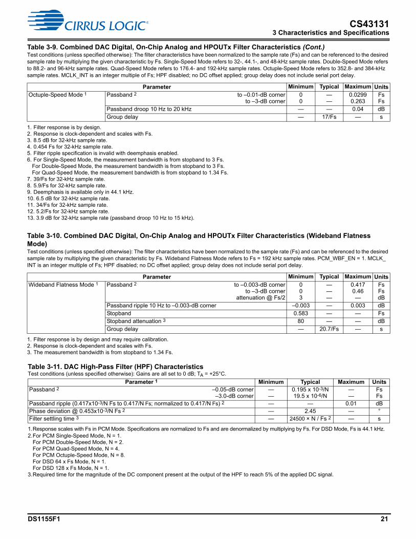
DS1155F1 21
CS431313 Characteristics and Specifications
Octuple-Speed Mode 1 Passband 2 to –0.01-dB cornerto –3-dB corner
00
——
0.02990.263
FsFs
Passband droop 10 Hz to 20 kHz — — 0.04 dBGroup delay — 17/Fs — s
1. Filter response is by design.2. Response is clock-dependent and scales with Fs.3. 8.5 dB for 32-kHz sample rate.4. 0.454 Fs for 32-kHz sample rate.5. Filter ripple specification is invalid with deemphasis enabled.6. For Single-Speed Mode, the measurement bandwidth is from stopband to 3 Fs.
For Double-Speed Mode, the measurement bandwidth is from stopband to 3 Fs.For Quad-Speed Mode, the measurement bandwidth is from stopband to 1.34 Fs.
7. 39/Fs for 32-kHz sample rate.8. 5.9/Fs for 32-kHz sample rate.9. Deemphasis is available only in 44.1 kHz. 10. 6.5 dB for 32-kHz sample rate.11. 34/Fs for 32-kHz sample rate.12. 5.2/Fs for 32-kHz sample rate.13. 3.9 dB for 32-kHz sample rate (passband droop 10 Hz to 15 kHz).
Table 3-10. Combined DAC Digital, On-Chip Analog and HPOUTx Filter Characteristics (Wideband Flatness Mode)Test conditions (unless specified otherwise): The filter characteristics have been normalized to the sample rate (Fs) and can be referenced to the desired sample rate by multiplying the given characteristic by Fs. Wideband Flatness Mode refers to Fs = 192 kHz sample rates. PCM_WBF_EN = 1. MCLK_INT is an integer multiple of Fs; HPF disabled; no DC offset applied; group delay does not include serial port delay.
Parameter Minimum Typical Maximum UnitsWideband Flatness Mode 1
1. Filter response is by design and may require calibration.
Passband 2
2. Response is clock-dependent and scales with Fs.
to –0.003-dB cornerto –3-dB corner
attenuation @ Fs/2
003
———
0.4170.46—
FsFsdB
Passband ripple 10 Hz to –0.003-dB corner –0.003 — 0.003 dBStopband 0.583 — — FsStopband attenuation 3
3. The measurement bandwidth is from stopband to 1.34 Fs.
80 — — dBGroup delay — 20.7/Fs — s
Table 3-11. DAC High-Pass Filter (HPF) CharacteristicsTest conditions (unless specified otherwise): Gains are all set to 0 dB; TA = +25°C.
Parameter 1
1.Response scales with Fs in PCM Mode. Specifications are normalized to Fs and are denormalized by multiplying by Fs. For DSD Mode, Fs is 44.1 kHz.
Minimum Typical Maximum UnitsPassband 2
2.For PCM Single-Speed Mode, N = 1.For PCM Double-Speed Mode, N = 2.For PCM Quad-Speed Mode, N = 4.For PCM Octuple-Speed Mode, N = 8.For DSD 64 x Fs Mode, N = 1.For DSD 128 x Fs Mode, N = 1.
–0.05-dB corner–3.0-dB corner
——
0.195 x 10⁻³/N 19.5 x 10⁻⁶/N
——
FsFs
Passband ripple (0.417x10⁻³/N Fs to 0.417/N Fs; normalized to 0.417/N Fs) 2 — — 0.01 dBPhase deviation @ 0.453x10⁻³/N Fs 2 — 2.45 — °Filter settling time 3
3.Required time for the magnitude of the DC component present at the output of the HPF to reach 5% of the applied DC signal.
— 24500 × N / Fs 2 — s
Table 3-9. Combined DAC Digital, On-Chip Analog and HPOUTx Filter Characteristics (Cont.)Test conditions (unless specified otherwise): The filter characteristics have been normalized to the sample rate (Fs) and can be referenced to the desired sample rate by multiplying the given characteristic by Fs. Single-Speed Mode refers to 32-, 44.1-, and 48-kHz sample rates. Double-Speed Mode refers to 88.2- and 96-kHz sample rates. Quad-Speed Mode refers to 176.4- and 192-kHz sample rates. Octuple-Speed Mode refers to 352.8- and 384-kHz sample rates. MCLK_INT is an integer multiple of Fs; HPF disabled; no DC offset applied; group delay does not include serial port delay.
Parameter Minimum Typical Maximum Units
22 DS1155F1
CS431313 Characteristics and Specifications
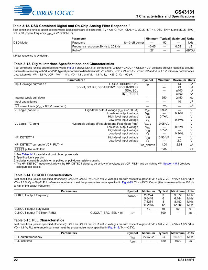
Table 3-12. DSD Combined Digital and On-Chip Analog Filter Response 1
Test conditions (unless specified otherwise): Digital gains are all set to 0 dB; TA = +25°C; PDN_XTAL = 0, MCLK_INT = 1, DSD_EN = 1, and MCLK_SRC_SEL = 00 (crystal frequency fXTAL = 22.5792 MHz).
1.Filter response is by design.
Parameter Minimum Typical Maximum UnitsDSD Mode Passband to –3-dB corner — 50 — kHz
Frequency response 20 Hz to 20 kHz –0.05 — 0.05 dBRoll-off 27 — — dB/Oct
Table 3-13. Digital Interface Specifications and CharacteristicsTest conditions (unless specified otherwise): Fig. 2-1 shows CS43131 connections; GNDD = GNDCP = GNDA = 0 V; voltages are with respect to ground; parameters can vary with VL and VP; typical performance data taken with VP = 3.6 V, VCP = VA = 1.8 V, VD = 1.8V and VL = 1.8 V; min/max performance data taken with VP = 3.6 V, VCP = VA = 1.8 V, VD = 1.8V and VL = 1.8 V; TA = +25°C; CL = 60 pF.
Parameters 1
1.See Table 1-1 for serial and control-port power rails.
Symbol Minimum Maximum UnitsInput leakage current 2,3
2.Specification is per pin. 3.Includes current through internal pull-up or pull-down resistors on pin.
LRCK1, DSDB/LRCK2SDIN1, SCLK1, DSDA/SDIN2, DSDCLK/SCLK2
SDA, SCLINT, RESET
Iin ————
±4 ±3
±100±100
µAµAnAnA
Internal weak pull-down — 550 2450 kInput capacitance — — 10 pF
INT current sink (VOL = 0.3 V maximum) — 825 — µA
VL Logic (non-I2C) High-level output voltage (IOH = –100 µA)Low-level output voltageHigh-level input voltageLow-level input voltage
VOHVOLVIHVIL
0.9•VL—
0.7•VL—
—0.1•VL
—0.3•VL
VVVV
VL Logic (I2C only) Hysteresis voltage (Fast Mode and Fast Mode Plus)Low-level output voltageHigh-level input voltageLow-level input voltage
VHYSVOLVIHVIL
0.05•VL—
0.7•VL—
—0.2•VL
—0.3•VL
VVVV
HP_DETECT 4
4.The HP_DETECT input circuit allows the HP_DETECT signal to be as low of a voltage as VCP_FILT– and as high as VP. Section 4.5.1 provides configuration details.
High-level input voltageLow-level input voltage
VIHVIL
0.93•VP—
—2.0
VV
HP_DETECT current to VCP_FILT– 4 IHP_DETECT 1.00 2.91 µA
RESET pulse width low — 1000 — µs
Table 3-14. CLKOUT CharacteristicsTest conditions (unless specified otherwise): GNDD = GNDCP = GNDA = 0 V; voltages are with respect to ground; VP = 3.6 V, VCP = VA = 1.8 V, VL = VD = 1.8 V; CL = 60 pF; PLL reference input must meet the phase-noise mask specified in Fig. 4-15; TA = +25°C; Output jitter is measured from 100 Hz to half of the output frequency.
Parameters Symbol Minimum Typical Maximum UnitsCLKOUT output frequency fCLKOUT 2.8224
5.64487.526411.2896
368
12
3.0726.1448.192
12.288
MHzMHzMHzMHz
CLKOUT output duty cycle — 40 50 60 %CLKOUT output TIE jitter (RMS) CLKOUT_SRC_SEL = 01 tJIT — 500 — ps
Table 3-15. PLL CharacteristicsTest conditions (unless specified otherwise): GNDD = GNDCP = GNDA = 0 V; voltages are with respect to ground; VP = 3.6 V, VCP = VA = 1.8 V, VL = VD = 1.8 V; PLL reference input must meet the phase-noise mask specified in Fig. 4-15; TA = +25°C.
Parameters Symbol Minimum Typical Maximum UnitsPLL output frequency fout 22.5792 24 24.576 MHzPLL lock time tLock — 620 1000 µs
DS1155F1 23
CS431313 Characteristics and Specifications
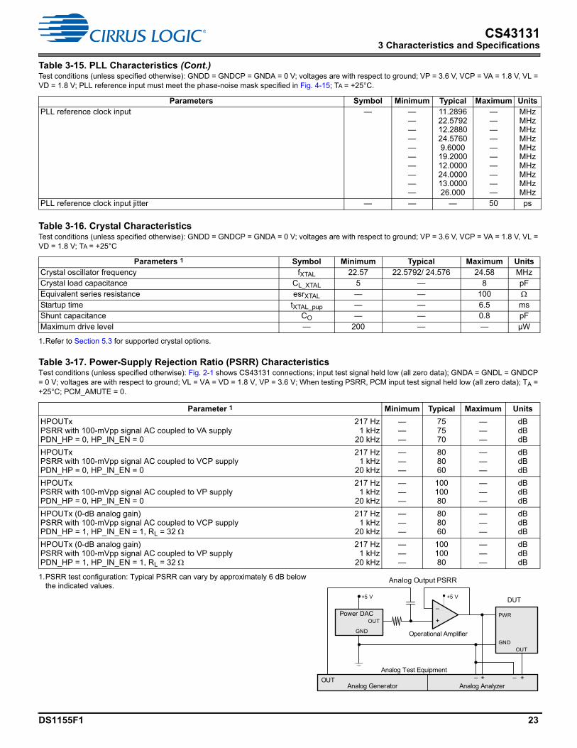
PLL reference clock input — ——————————
11.289622.579212.288024.57609.600019.200012.000024.000013.000026.000
——————————
MHzMHzMHzMHzMHzMHzMHzMHzMHzMHz
PLL reference clock input jitter — — — 50 ps
Table 3-16. Crystal CharacteristicsTest conditions (unless specified otherwise): GNDD = GNDCP = GNDA = 0 V; voltages are with respect to ground; VP = 3.6 V, VCP = VA = 1.8 V, VL = VD = 1.8 V; TA = +25°C
Parameters 1
1.Refer to Section 5.3 for supported crystal options.
Symbol Minimum Typical Maximum UnitsCrystal oscillator frequency fXTAL 22.57 22.5792/ 24.576 24.58 MHzCrystal load capacitance CL_XTAL 5 — 8 pFEquivalent series resistance esrXTAL — — 100 Startup time tXTAL_pup — — 6.5 msShunt capacitance CO — — 0.8 pFMaximum drive level — 200 — — µW
Table 3-17. Power-Supply Rejection Ratio (PSRR) CharacteristicsTest conditions (unless specified otherwise): Fig. 2-1 shows CS43131 connections; input test signal held low (all zero data); GNDA = GNDL = GNDCP = 0 V; voltages are with respect to ground; VL = VA = VD = 1.8 V, VP = 3.6 V; When testing PSRR, PCM input test signal held low (all zero data); TA = +25°C; PCM_AMUTE = 0.
Parameter 1
1.PSRR test configuration: Typical PSRR can vary by approximately 6 dB below the indicated values.
Minimum Typical Maximum Units
HPOUTxPSRR with 100-mVpp signal AC coupled to VA supplyPDN_HP = 0, HP_IN_EN = 0
217 Hz1 kHz
20 kHz
———
757570
———
dBdBdB
HPOUTxPSRR with 100-mVpp signal AC coupled to VCP supplyPDN_HP = 0, HP_IN_EN = 0
217 Hz1 kHz
20 kHz
———
808060
———
dBdBdB
HPOUTxPSRR with 100-mVpp signal AC coupled to VP supplyPDN_HP = 0, HP_IN_EN = 0
217 Hz1 kHz
20 kHz
———
10010080
———
dBdBdB
HPOUTx (0-dB analog gain)PSRR with 100-mVpp signal AC coupled to VCP supplyPDN_HP = 1, HP_IN_EN = 1, RL = 32
217 Hz1 kHz
20 kHz
———
808060
———
dBdBdB
HPOUTx (0-dB analog gain)PSRR with 100-mVpp signal AC coupled to VP supplyPDN_HP = 1, HP_IN_EN = 1, RL = 32
217 Hz1 kHz
20 kHz
———
10010080
———
dBdBdB
Table 3-15. PLL Characteristics (Cont.)Test conditions (unless specified otherwise): GNDD = GNDCP = GNDA = 0 V; voltages are with respect to ground; VP = 3.6 V, VCP = VA = 1.8 V, VL = VD = 1.8 V; PLL reference input must meet the phase-noise mask specified in Fig. 4-15; TA = +25°C.
Parameters Symbol Minimum Typical Maximum Units
Operational Amplifier
OUT
GND
Power DAC
OUTGND
PWR
DUT+5 V +5 V
++ ––
+
–
OUTAnalog Generator Analog Analyzer
Analog Test Equipment
Analog Output PSRR
24 DS1155F1
CS431313 Characteristics and Specifications
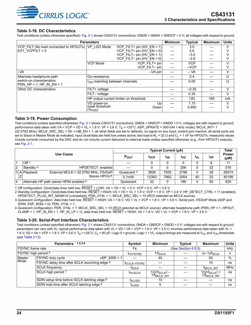
Table 3-18. DC CharacteristicsTest conditions (unless otherwise specified): Fig. 2-1 shows CS43131 connections; GNDD = GNDA = GNDCP = 0 V; all voltages with respect to ground.
Parameters Minimum Typical Maximum UnitsVCP_FILT (No load connected to HPOUTx)EXT_VCPFILT = 0
VP_LDO Mode VCP_FILT+ pin (HV_EN = 1)VCP_FILT+ pin (HV_EN = 0)VCP_FILT– pin (HV_EN = 1)VCP_FILT– pin (HV_EN = 0)
————
3.02.6–3.0–2.6
————
VVVV
VCP Mode VCP_FILT+ pinVCP_FILT– pin
——
VCP–VCP
——
VV
–VA –VA pin — – VA — VAlternate headphone pathswitch-on characteristicsPDN_HP = 1, HP_IN_EN = 1
On-resistance — 0.4 — rON matching between channels — 0.05 —
Other DC characteristics FILT+ voltage — –0.35 — VFILT– voltage — 0.35 — VHP output current limiter on threshold. — 120 160 mAVD power-on reset threshold (VPOR)
UpDown
——
1.150.950
——
VV
Table 3-19. Power ConsumptionTest conditions (unless specified otherwise): Fig. 2-1 shows CS43131 connections; GNDA = GNDCP = GNDD = 0 V; voltages are with respect to ground; performance data taken with VA = VCP = VD = VL = 1.8 V; VP = 3.6 V; TA = +25°C; ASP_SPRATE = 0001(44.1-kHz mode); MCLK_INT= 1 (22.5792 MHz); MCLK_SRC_SEL = 00; +1dB_EN = 1; all other fields are set to defaults; no signal on any input; control port inactive; all serial ports are set to Slave or Master Mode as indicated, input clock/data are held low unless active; test load is RL = 32 and CL = 1 nF for HPOUTx; measured values include currents consumed by the DAC and do not include current delivered to external loads unless specified otherwise (e.g., from HPOUTx outputs); see Fig. 2-1.
Use CasesTypical Current (µA) Total
Power(µW)POUT iVCP iVA iVD iVL iVP
1 Off 1
1.Off configuration: Clock/data lines held low; RESET = LOW; VA = VD = VL = 0 V, VCP = 0 V, VP = 3.6 V.
— 0 0 0 0 6 112 Standby 2
2.Standby configuration: Clock/data lines held low; RESET = HIGH; VA = VD = VL = 1.8 V, VCP = 1.8 V, VP = 3.6 V; HP_DETECT_CTRL = 11 (enabled); HPDETECT_PLUG_INT_MASK=0 (unmasked); PDN_XTAL = 1, MCLK_SRC_SEL = 10 (RCO selected as MCLK source).
HPDETECT enabled — 0 0 256 0 32 5763 A Playback External MCLK = 22.5792 MHz, I2S/DoP
Stereo HPOUTQuiescent 3
3.Quiescent configuration: data lines held low; RESET = HIGH; VA = 1.8 V, VD = VL = VCP = 1.8 V, VP = 3.6 V. Serial port, I2S/DoP Mode (ASP and SDIN, ASP_M/Sb = 0); PDN_XTAL = 1.
3808 7835 2786 0 28 26074C 0.1mW 12363 7862 2004 40 32 40199
4 Alternate HP path stereo HPIN enabled 4
4.Quiescent configuration: PDN_XTAL = 1; MCLK_SRC_SEL = 10 (RCO selected as MCLK source); alternate headphone path (PDN_HP = 1, HPOUT_CLAMP = 1, HP_IN_EN = 1, HP_IN_LP = 1); data lines held low; RESET = HIGH; VA = 1.8 V, VD = VL = VCP = 1.8 V, VP = 3.6 V.
Quiescent 32 0 186 0 65 625
Table 3-20. Serial-Port Interface CharacteristicsTest conditions (unless specified otherwise): Fig. 2-1 shows CS43131 connections; GNDA = GNDCP = GNDD = 0 V; voltages are with respect to ground; parameters can vary with VL; typical performance data taken with VL = VD = VA = VCP = 1.8 V, VP = 3.6 V; min/max performance data taken with VL = 1.8 V; VD = VA = VCP = 1.8 V, VP = 3.6 V; TA = +25°C; CL = 60 pF; Logic 0 = ground, Logic 1 = VL; output timings are measured at VOL and VOH thresholds (see Table 3-13).
Parameters 1,2,3,4 Symbol Minimum Typical Maximum UnitsFSYNC frame rate Fs (See Section 4.9.5) kHzFSYNC high period 5 tHI:FSYNC 1/fSCLK — (n–1)/fSCLK sMaster Mode
FSYNC duty cycle xSP_5050 = 1 — 45 — 55 %FSYNC delay time after SCLK launching edge 6 tD:CLK–FSYNC — — 10 nsSCLK frequency fSCLK — — fMCLK_INT MHzSCLK high period 7 tHI:SCLK 1/(2•fSCLK) –
1/fMCLK_INT— 1/(2•fSCLK) +
1/fMCLK_INTns
SDIN setup time before SCLK latching edge 6 tSU:SDI 10 — — nsSDIN hold time after SCLK latching edge 6 tH:SDI 5 — — ns
DS1155F1 25
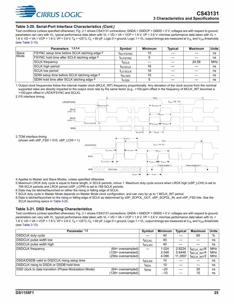
CS431313 Characteristics and Specifications
Slave Mode
FSYNC setup time before SCLK latching edge 6 tSU:FSYNC 10 — — nsFSYNC hold time after SCLK latching edge 6 tH:FSYNC 5 — — nsSCLK frequency fSCLK — — 24.58 MHzSCLK high period tHI:SCLK 16 — — nsSCLK low period tLO:SCLK 16 — — nsSDIN setup time before SCLK latching edge 8 tSU:SDI 10 — — nsSDIN hold time after SCLK latching edge 6 tH:SDI 5 — — ns
1.Output clock frequencies follow the internal master clock (MCLK_INT) frequency proportionally. Any deviation of the clock source from the nominal supported rates are directly imparted to the output clock rate by the same factor (e.g., +100-ppm offset in the frequency of MCLK_INT becomes a +100-ppm offset in LRCK/FSYNC and SCLK).
2.I2S interface timing
3.TDM interface timing(shown with xSP_FSD = 010, xSP_LCHI = 1)
4.Applies to Master and Slave Modes, unless specified otherwise.5.Maximum LRCK duty cycle is equal to frame length, in SCLK periods, minus 1. Maximum duty cycle occurs when LRCK high (xSP_LCHI) is set to
768 SCLK periods and LRCK period (xSP_LCPR) is set to 769 SCLK periods.6.Data may be latched/launched on either the rising or falling edge of SCLK.7.SCLK duty cycle in Master Mode depends on Master Mode clock configuration, and can vary by up to 1 MCLK_INT period.8.Data is latched/launched on the rising or falling edge of SCLK as determined by xSP_SCPOL_OUT, xSP_SCPOL_IN, and xSP_FSD bits. See the
SCLK launching specs in Table 3-20.
Table 3-21. DSD Switching CharacteristicsTest conditions (unless specified otherwise): Fig. 2-1 shows CS43131 connections; GNDA = GNDCP = GNDD = 0 V; voltages are with respect to ground; parameters can vary with VL; typical performance data taken with VL = VD = VA = VCP = 1.8 V, VP = 3.6 V; min/max performance data taken with VL = 1.8 V; VD = VA = VCP = 1.8 V, VP = 3.6 V; TA = +25°C; CL = 60 pF; Logic 0 = ground, Logic 1 = VL; output timings are measured at VOL and VOH thresholds (see Table 3-13).
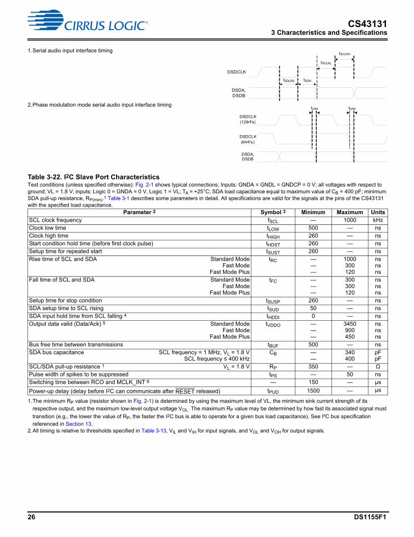
Parameter 1,2 Symbol Minimum Typical Maximum UnitsDSDCLK duty cycle — 40 — 60 %DSDCLK pulse width low tSCLKL 40 — — nsDSDCLK pulse width high tSCLKH 40 — — nsDSDCLK frequency (64× oversampled)
(128× oversampled)(256x oversampled)
— 1.0242.0484.096
2.82245.644811.2897
fMCLK_INT/8fMCLK_INT/4fMCLK_INT/2
MHzMHzMHz
DSDA/DSDB valid to DSDCLK rising setup time tSDLRS 10 — — nsDSDCLK rising to DSDA or DSDB hold time tSDH 10 — — nsDSD clock to data transition (Phase Modulation Mode) (64× oversampled)
(128× oversampled)tDPM –20
–10——
2010
nsns
Table 3-20. Serial-Port Interface Characteristics (Cont.)Test conditions (unless specified otherwise): Fig. 2-1 shows CS43131 connections; GNDA = GNDCP = GNDD = 0 V; voltages are with respect to ground; parameters can vary with VL; typical performance data taken with VL = VD = VA = VCP = 1.8 V, VP = 3.6 V; min/max performance data taken with VL = 1.8 V; VD = VA = VCP = 1.8 V, VP = 3.6 V; TA = +25°C; CL = 60 pF; Logic 0 = ground, Logic 1 = VL; output timings are measured at VOL and VOH thresholds (see Table 3-13).
Parameters 1,2,3,4 Symbol Minimum Typical Maximum Units
SCLK(CPOL = 1)
SDIN
tSU:SDI tH:SDI
LRCK/FSYNC
tD:CLK–FSYNC
1/Fs
...
...
fSCLK = N · Fs
tSU:FSYNC tH:FSYNC
tLO:SCLK tHI:SCLK
SCLK(CPOL = 0)
...
1/fSCLK
...
...
...
...
...
SCLK
SDIN
tSU:SDI tH:SDI
LRCK/FSYNC
tD:CLK-FSYNC
1/fSCLK
Don’t Care
Frame location 0 Frame location N -1
1/Fs
...
...
...
fSCLK = N · Fs
tSU :FSYNC tH:FSYNC
tHI:FSYNC
tLO:SCLK tHI:SCLK
26 DS1155F1
CS431313 Characteristics and Specifications
1.Serial audio input interface timing
2.Phase modulation mode serial audio input interface timing
Table 3-22. I2C Slave Port CharacteristicsTest conditions (unless specified otherwise): Fig. 2-1 shows typical connections; Inputs: GNDA = GNDL = GNDCP = 0 V; all voltages with respect to ground; VL = 1.8 V; inputs: Logic 0 = GNDA = 0 V, Logic 1 = VL; TA = +25°C; SDA load capacitance equal to maximum value of CB = 400 pF; minimum SDA pull-up resistance, RP(min).1 Table 3-1 describes some parameters in detail. All specifications are valid for the signals at the pins of the CS43131 with the specified load capacitance.
1.The minimum RP value (resistor shown in Fig. 2-1) is determined by using the maximum level of VL, the minimum sink current strength of its respective output, and the maximum low-level output voltage VOL. The maximum RP value may be determined by how fast its associated signal must
transition (e.g., the lower the value of RP, the faster the I2C bus is able to operate for a given bus load capacitance). See I²C bus specification referenced in Section 13.
Parameter 2
2.All timing is relative to thresholds specified in Table 3-13, VIL and VIH for input signals, and VOL and VOH for output signals.
Symbol 3 Minimum Maximum UnitsSCL clock frequency fSCL — 1000 kHzClock low time tLOW 500 — nsClock high time tHIGH 260 — nsStart condition hold time (before first clock pulse) tHDST 260 — nsSetup time for repeated start tSUST 260 — nsRise time of SCL and SDA Standard Mode
Fast ModeFast Mode Plus
tRC ———
1000300120
nsnsns
Fall time of SCL and SDA Standard ModeFast Mode
Fast Mode Plus
tFC ———
300300120
nsnsns
Setup time for stop condition tSUSP 260 — nsSDA setup time to SCL rising tSUD 50 — nsSDA input hold time from SCL falling 4 tHDDI 0 — nsOutput data valid (Data/Ack) 5 Standard Mode
Fast ModeFast Mode Plus
tVDDO ———
3450900450
nsnsns
Bus free time between transmissions tBUF 500 — nsSDA bus capacitance SCL frequency = 1 MHz, VL = 1.8 V
SCL frequency ≤ 400 kHzCB —
—340400
pFpF
SCL/SDA pull-up resistance 1 VL = 1.8 V RP 350 — ΩPulse width of spikes to be suppressed tPS — 50 nsSwitching time between RCO and MCLK_INT 6 — 150 — µs
Power-up delay (delay before I2C can communicate after RESET released) tPUD 1500 — µs
DSDCLK
DSDA, DSDB
tSDLRS tSDH
tSCLKL
tSCLKH
DSDCLK(128•Fs)
DSDCLK(64•Fs)
DSDA, DSDB
tDPM tDPM
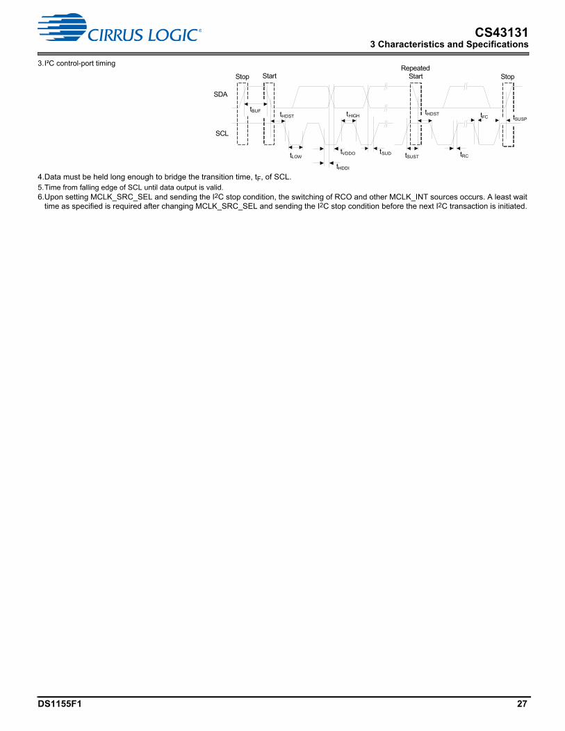
DS1155F1 27
CS431313 Characteristics and Specifications
3.I²C control-port timing
4.Data must be held long enough to bridge the transition time, tF, of SCL.5.Time from falling edge of SCL until data output is valid.6.Upon setting MCLK_SRC_SEL and sending the I2C stop condition, the switching of RCO and other MCLK_INT sources occurs. A least wait
time as specified is required after changing MCLK_SRC_SEL and sending the I2C stop condition before the next I2C transaction is initiated.
tBUF
tLOW
Stop
tHDDI
tSUD tSUST tRC
tHDST tHIGHtHDST tFC tSUSP
StartRepeated
Start Stop
SDA
SCL
tVDDO
28 DS1155F1
CS431314 Functional Description
4 Functional Description
This section describes the general theory of operation of the CS43131, tracing the signal and control flow through the various blocks within the device. It comprises the following sections:
• Section 4.1, “Overview”
• Section 4.2, “Analog Outputs”
• Section 4.3, “Class H Amplifier Output”
• Section 4.4, “Alternate Headphone Inputs”
• Section 4.5, “Headphone Presence Detect and Output Load Detection”
• Section 4.6, “Clocking Architecture”
• Section 4.7, “Clock Output and Fractional-N PLL”
• Section 4.8, “Filtering Options”
• Section 4.9, “Audio Serial Port (ASP)”
• Section 4.10, “DSD Interface”
• Section 4.11, “DSD and PCM Mixing”
• Section 4.12, “Standard Interrupts”
• Section 4.13, “Control Port Operation”
• Section 4.14, “Programmable Filter”
4.1 Overview
4.1.1 Analog Outputs
The analog output block includes separate pseudodifferential headphone Class H amplifiers output. An on-chip inverting charge pump creates a positive and negative voltage equal to the input, allowing an adaptable, full-scale output swing centered around ground. The resulting internal amplifier supply can be ±VCP, or ±VP_LDO (either ±3.0 V with HV_EN = 1 or ±2.6 V with HV_EN = 0).
The inverting architecture eliminates the need for large DC-blocking capacitors and allows the amplifier to deliver more power to HP loads at lower supply voltages. This adaptive power supply scheme converts traditional Class AB amplifiers into more power-efficient Class H amplifiers.
4.1.2 Alternate Headphone Inputs
The alternate headphone inputs provide an integrated selectable path to interface between the system codec output and the headphone connector, which allows for lower-power operation in applications such as voice or compressed music playback. These inputs eliminate the need for an external audio switch and prevent the high-fidelity headphone outputs of CS43131 from degradation by the external audio switch.
4.1.3 Headphone Detection
The CS43131 detects the presence of a headphone and notifies the application processor to wake up through an interrupt event.
4.1.4 Headphone Impedance Measurement
The CS43131 detects headphone impedance information at low frequencies, which can be used to adjust the system properly to accommodate different load conditions. One example is to adjust signal chain gain to avoid distortion.
The CS43131 also provides impedance measurement functions to evaluate the headphone load within 20 Hz to 20 kHz. A specific frequency is selected and the impedance measurement process is initiated by setting the register. Through a series of interrupt events, the CS43131 notifies application processor to retrieve the impedance information after completion.
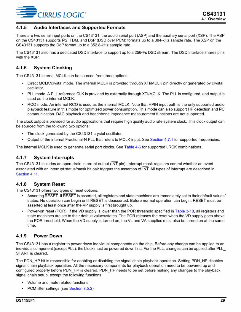
DS1155F1 29
CS431314.1 Overview
4.1.5 Audio Interfaces and Supported Formats
There are two serial input ports on the CS43131, the audio serial port (ASP) and the auxiliary serial port (XSP). The ASP on the CS43131 supports I2S, TDM, and DoP (DSD over PCM) formats up to a 384-kHz sample rate. The XSP on the CS43131 supports the DoP format up to a 352.8-kHz sample rate.
The CS43131 also has a dedicated DSD interface to support up to a 256•Fs DSD stream. The DSD interface shares pins with the XSP.
4.1.6 System Clocking
The CS43131 internal MCLK can be sourced from three options:
• Direct MCLK/crystal mode. The internal MCLK is provided through XTI/MCLK pin directly or generated by crystal oscillator.
• PLL mode. A PLL reference CLK is provided by externally through XTI/MCLK. The PLL is configured, and output is used as the internal MCLK.
• RCO mode. An internal RCO is used as the internal MCLK. Note that HPIN input path is the only supported audio playback feature in this mode for optimized power consumption. This mode can also support HP detection and I2C communication. DAC playback and headphone impedance measurement functions are not supported.
The clock output is provided for audio applications that require high quality audio rate system clock. This clock output can be sourced from the following two options:
• The clock generated by the CS43131 crystal oscillator.
• Output of the internal Fractional-N PLL that refers to MCLK input. See Section 4.7.1 for supported frequencies.
The internal MCLK is used to generate serial port clocks. See Table 4-6 for supported LRCK combinations.
4.1.7 System InterruptsThe CS43131 includes an open-drain interrupt output (INT pin). Interrupt mask registers control whether an event associated with an interrupt status/mask bit pair triggers the assertion of INT. All types of interrupt are described in Section 4.11.
4.1.8 System ResetThe CS43131 offers two types of reset options:
• Asserting RESET. If RESET is asserted, all registers and state machines are immediately set to their default values/states. No operation can begin until RESET is deasserted. Before normal operation can begin, RESET must be asserted at least once after the VP supply is first brought up.
• Power-on reset (POR). If the VD supply is lower than the POR threshold specified in Table 3-18, all registers and state machines are set to their default values/states. The POR releases the reset when the VD supply goes above the POR threshold. When the VD supply is turned on, the VL and VA supplies must also be turned on at the same time.
4.1.9 Power Down
The CS43131 has a register to power down individual components on the chip. Before any change can be applied to an individual component (except PLL), the block must be powered down first. For the PLL, changes can be applied after PLL_START is cleared.
The PDN_HP bit is responsible for enabling or disabling the signal chain playback operation. Setting PDN_HP disables signal chain playback operation. All the necessary components for playback operation need to be powered up and configured properly before PDN_HP is cleared. PDN_HP needs to be set before making any changes to the playback signal chain setup, except the following functions:
• Volume and mute related functions
• PCM filter settings (see Section 7.5.2)
30 DS1155F1
CS431314.1 Overview
Before ASP, XSP, or DSDIF can be safely powered down, PDN_HP must be asserted, and PDN_DONE_INT must be present. For XTAL or PLL used as the source of internal MCLK, PDN_HP needs to be set first and MCLK source needs to be properly switched away before PDN_XTAL or PDN_PLL is set. If PLL output is only used as the source of CLKOUT, PDN_PLL can be set without PDN_HP being asserted. If the steps described above are not followed, the CS43131 enters an unresponsive state.
PDN_CLKOUT does not require PDN_HP to be set before it is enabled.
PDN_HP should be set before using headphone input path and load detection function. Refer to the functional description of these two components for further details.
Recommended power-up and power-down sequences can be found in the Section 5.2.
DS1155F1 31
CS431314.2 Analog Outputs
4.2 Analog Outputs
The CS43131 provides an analog output that is derived from the digital audio input ports. This section describes the general flow of the analog outputs.
4.2.1 Analog Output Signal Flow
The CS43131 signal flow is shown in Fig. 4-1.
Figure 4-1. Analog Output Signal Flow
The CS43131 has 4 settings of full scale voltage, which are determined by OUT_FS[1:0]. When OUT_FS[1:0] = 11 and HV_EN = 1, the +1dB_EN bit can boost the output voltage to 2 Vrms. In any other setting combination of OUT_FS[1:0] and HV_EN, the +1dB_EN bit is ignored. The proper full scale voltage must be set first, and the digital volume settings is used to control signal levels.
The CS43131 digital volume control allows independent control of the signal level in 1/2 dB increments from 0 dB (0b0000 0000) to –127 dB (0b1111 1110) by using x_VOLUME_y (where "x" is either PCM or DSD; "y" is either A or B) register. When the x_VOL_BEQA bit is set, both volumes can be changed simultaneously using x_VOLUME_A). The volume changes are implemented as dictated by PCM_SZC[1:0] and DSD_SZC in the signal control register (see Section 7.4.3 and Section 7.5.5). If soft ramping is enabled, gain and attenuation changes are carried out by incrementally changing the volume level in 1/8-dB steps, from the previous level to the new level. For PCM, when PCM_SZC[1:0] = 2, the volume level changes at an approximate rate of 1 dB/ms. The volume level also changes at a rate of 1 dB/ms for DSD. Both channels can be inverted independently by setting the INV_A and INV_B bits. Both channels can be swapped by setting the x_SWAP_CHAN bit. Channel A content can be copied to channel B by setting the x_COPY_CHAN bit. Mono mode can be enabled with proper setting of these bits.
The CS43131 provides individual ramp-up and ramp-down control options (from the global soft ramp settings) for two specific scenarios. The PCM_RAMP_DOWN bit is for the scenario when the interpolation filter configuration switches (as configured by the PCM Filter Option register) during PCM playback. DSD_RAMP_UP bit is for the scenario when DSD playback recovers from detected DSD stream errors. Refer to each individual register description for setting details.
The CS43131 can mute both channels simultaneously or independently. Also, it can auto-mute on both PCM stream and DSD stream when mute pattern is identified (defined in PCM_AMUTE and DSD_AMUTE). Additional signal and mute control options can be found in Section 7.4.3 and Section 7.5.5.
Multibit
Modulator
Multibit
Modulator
InterpolationFilter & Volume Control
InterpolationFilter & Volume Control
DAC and Filter
DAC and Filter
–
+
–
+
HPINB
HPINA
HPOUTA
HPOUTB
DSD Processor
DoP to DSD
Engine
MU
X
Audio Source
I2S
HPREFB
HPREFA
DoP
DSD
HP_IN_EN p. 127HP_IN_LP p. 127
HP_IN_EN p. 127HP_IN_LP p. 127
PDN_HP
DSD_EN p. 126
MIX_PCM_PREP p. 126MIX_PCM_DSD p. 126
PCM_SZC p. 129PCM_RAMP_DOWN p. 129PCM_VOLUME_B p. 128PCM_VOLUME_A p. 128PCM_INV_A p. 129PCM_INV_B p. 129PCM_SWAP_CHAN p. 129PCM_COPY_CHAN p. 129PCM_VOL_BEQA p. 129PCM_AMUTE p. 129PCM_AMUTEBEQA p. 129PCM_MUTE_A p. 129PCM_MUTE_B p. 129FILTER_SLOW_FASTB p. 128PHCOMP_LOWLATB p. 128HIGH_PASS p. 128DEEMP_ON p. 128NOS p. 128
DAC_OVFL_INT p. 134
DSD_PRC_SRC p. 126
DSD_SPEED p. 126STA_DSD_DET p. 126INV_DSD_DET p. 126
DSD_VOLUME_B p. 124DSD_VOLUME_A p. 125DSD_INV_A p. 127DSD_INV_B p. 127DSD_VOL_BEQA p. 125DSD_AMUTE p. 125DSD_MUTE_A p. 125
+1dB_EN p. 127OUT_FS p. 127PCM_WBF_EN p. 128
PDN_HP
DSD_MUTE_B p. 125DSD_ZERODB p. 126DSD_HPF_EN p. 127OUT_FS p. 127DSD_SZC p. 125DSD_RAMP_UP p. 125DSD_SWAP_CHAN p. 127DSD_COPY_CHAN p. 127
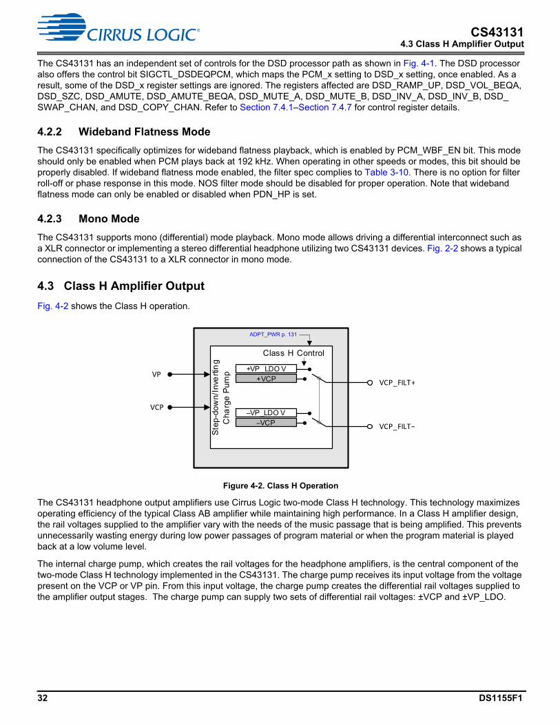
32 DS1155F1
CS431314.3 Class H Amplifier Output
The CS43131 has an independent set of controls for the DSD processor path as shown in Fig. 4-1. The DSD processor also offers the control bit SIGCTL_DSDEQPCM, which maps the PCM_x setting to DSD_x setting, once enabled. As a result, some of the DSD_x register settings are ignored. The registers affected are DSD_RAMP_UP, DSD_VOL_BEQA, DSD_SZC, DSD_AMUTE, DSD_AMUTE_BEQA, DSD_MUTE_A, DSD_MUTE_B, DSD_INV_A, DSD_INV_B, DSD_SWAP_CHAN, and DSD_COPY_CHAN. Refer to Section 7.4.1–Section 7.4.7 for control register details.
4.2.2 Wideband Flatness Mode
The CS43131 specifically optimizes for wideband flatness playback, which is enabled by PCM_WBF_EN bit. This mode should only be enabled when PCM plays back at 192 kHz. When operating in other speeds or modes, this bit should be properly disabled. If wideband flatness mode enabled, the filter spec complies to Table 3-10. There is no option for filter roll-off or phase response in this mode. NOS filter mode should be disabled for proper operation. Note that wideband flatness mode can only be enabled or disabled when PDN_HP is set.
4.2.3 Mono Mode
The CS43131 supports mono (differential) mode playback. Mono mode allows driving a differential interconnect such as a XLR connector or implementing a stereo differential headphone utilizing two CS43131 devices. Fig. 2-2 shows a typical connection of the CS43131 to a XLR connector in mono mode.
4.3 Class H Amplifier Output
Fig. 4-2 shows the Class H operation.
Figure 4-2. Class H Operation
The CS43131 headphone output amplifiers use Cirrus Logic two-mode Class H technology. This technology maximizes operating efficiency of the typical Class AB amplifier while maintaining high performance. In a Class H amplifier design, the rail voltages supplied to the amplifier vary with the needs of the music passage that is being amplified. This prevents unnecessarily wasting energy during low power passages of program material or when the program material is played back at a low volume level.
The internal charge pump, which creates the rail voltages for the headphone amplifiers, is the central component of the two-mode Class H technology implemented in the CS43131. The charge pump receives its input voltage from the voltage present on the VCP or VP pin. From this input voltage, the charge pump creates the differential rail voltages supplied to the amplifier output stages. The charge pump can supply two sets of differential rail voltages: ±VCP and ±VP_LDO.
VCP
Class H Control
Ste
p-do
wn/
Inve
rtin
g C
harg
e P
um
p
VCP_FILT––VCP–VP_LDO V
VCP_FILT++VCP+VP_LDO V
VP
ADPT_PWR p. 131

DS1155F1 33
CS431314.3 Class H Amplifier Output
HV_EN setting, as shown in Fig. 4-3, determines the VP_LDO voltage as shown in Table 4-1. HV_EN = 1 setting is required to support the 1.7-V full-scale voltage for a 600- load and above. In this setting, minimum VP is required to be higher than 3.3 V, and any load below 600 is not supported. When HV_EN = 0, the max output voltage is 1.4-V RMS full-scale voltage. In this setting, minimum VP is required to be higher than 3 V, and the full headphone load range is supported.
Figure 4-3. Internal LDO Configuration
Table 4-2 shows the nominal signal and volume level ranges when the output is set to the adapt modes explained in Section 4.3.1. If the signal level is greater than the maximum value of this range, then clipping can occur.
4.3.1 Power Supply Control Options
This section describes the two types of operation: standard Class AB and adapt-to-output signal. The set of rail voltages supplied to the amplifier output stages depends on the ADPT_PWR (see p. 131) setting.
4.3.1.1 Standard Class AB Operation (ADPT_PWR = 001 or 010)
If ADPT_PWR is set to 001 or 010, the rail voltages supplied to the amplifiers are held to ±VP_LDO or ±VCP, respectively. The rail voltages supplied to the output stages are held constant, regardless of the output signal level. The CS43131 amplifiers simply operate in a traditional Class AB configuration.
4.3.1.2 Adapt-to-Output Signal (ADPT_PWR = 111)
If ADPT_PWR is set to 111, the rail voltage sent to the amplifiers is based solely on whether the signal sent to the amplifiers would cause the amplifiers to clip when operating on the lower set of rail voltages at certain threshold values.
• If it would cause clipping, the control logic instructs the charge pump to provide the next higher set of rail voltages to the amplifiers.
• If it would not cause clipping, the control logic instructs the charge pump to provide the lower set of rail voltages to the amplifiers, eliminating the need to advise the CS43131 of volume settings external to the device.
Table 4-1. VP_LDO Voltage Per HV_EN Setting
HV_EN VP_LDO Voltage0 2.6 V1 3.0 V
Table 4-2. Class H Supply Modes
Mode Class H Supply Level Signal 1 or Volume Level Range 2,3,4
1.In adapt-to-signal, the volume level ranges are approximations but are within –0.5 dB from the values shown.2.Relative to digital full scale with output gain set to 0 dB.3.In fixed modes, clipping can occur if the signal level exceeds the maximum of this range due to setting the
amplifier’s supply too low.4.Thresholds shown are nominal for a 16-Ω stereo load.
0 ±VP_LDO V, internally regulated from VP –11 dB1 ±VCP < –11 dB
VP VP_LDOInternal LDO
HV_EN p. 131

34 DS1155F1
CS431314.3 Class H Amplifier Output
4.3.2 Power-Supply Transitions
Charge-pump transitions from the lower to the higher set of rail voltages occur on the next FLYN/FLYP clock cycle. Despite the system’s fast response time, the VCP_FILT pin’s capacitive elements prevent rail voltages from changing instantly. Instead, the rail voltages ramp up from the lower to the higher supply, based on the time constant created by the output impedance of the charge pump and the capacitor on the VCP_FILT pin (the transition time is approximately 20 µs).
Fig. 4-4 shows Class H supply switching. During this charging transition, a high dv/dt transient on the inputs may briefly clip the outputs before the rail voltages charge to the full higher supply level. This transitory clipping has been found to be inaudible in listening tests.
Figure 4-4. VCP_FILT Transitions
When the charge pump transitions from the lower to higher set or rail voltage, there is no delay associated with the transition.
+VCP
Ideal Transition
Actual Transition caused by VCP_FILT+ Capacitor Time
+VP_LDO
-VCP
-VP_LDO

DS1155F1 35
CS431314.3 Class H Amplifier Output
When the charge pump transitions from the higher to the lower set of rail voltages, there is an approximate 5.5-s delay before the charge pump supplies the lower rail voltages to the amplifiers. This hysteresis ensures that the charge pump does not toggle between the two rail voltages as signals approach the clip threshold. It also prevents clipping in the instance of repetitive high-level transients in the input signal. Fig. 4-5 shows examples of this transitional behavior.
Figure 4-5. VCP_FILT Hysteresis
Output Level
+VCP
Output Stage Rail Voltage
Time
–VCP
5.5 s
–11 dB
+VP_LDO
–VP_LDO
–11.5 dB

36 DS1155F1
CS431314.3 Class H Amplifier Output
4.3.3 HP Current Limiter
The CS43131 features built-in current-limit protection for the headphone output. Table 3-18 lists the threshold for the current limit during the short-circuit conditions shown in Fig. 4-6. For the HP amplifiers, current is from the internal charge pump output, and, as such, applies the current from VCP or VP.
Figure 4-6. HP Short Circuit Setup
4.3.4 External VCP_FILT Supply Mode
To bypass the CS43131 Class-H charge-pump circuit, provide external VCP_FILT± supply with the following conditions:
• When CS43131 is operating, apply +3.0 V with ±5% accuracy to VCP_FILT+ and apply –3.0 V with ±5% accuracy to VCP_FILT–.
• When CS43131 is powered down, external circuits present Hi-Z state to the VCP_FILT+ pin (>1k impedance) and VCP_FILT– pin (>10k impedance).
• To avoid possible damage, VCP_FILT± pins must remain within the absolute maximum rating specified.
Figure 4-7. External VCP_FILT Power-Up Sequence
For powering up CS43131 in this mode, the recommended sequence must be followed. This assumes that the CS43131 starts from the status where VCP_FILT± pins are presented with Hi-Z.
1. Set EXT_VCPFILT and HV_EN bits.
2. Wait 8 ms after I2C ACK.
3. Release and start to ramp external voltage on VCP_FILT± pins.
4. Wait until VCP_FILT+ pin voltage to be greater than +2.6V and VCP_FILT– to be less than –2.6 V.
GNDA/GNDCP
HPOUTA
HPOUTB
Charge Pump
I
I
VCP
VCP_FILT–
VCP_FILT+
VP
EXT_VCPFILT
PDN_HP
VCP_FILT+
VCP_FILT‐
8 ms
+3.0 V
‐3.0 V
+2.6 V
‐2.6 V
Hi‐Z
Hi‐Z
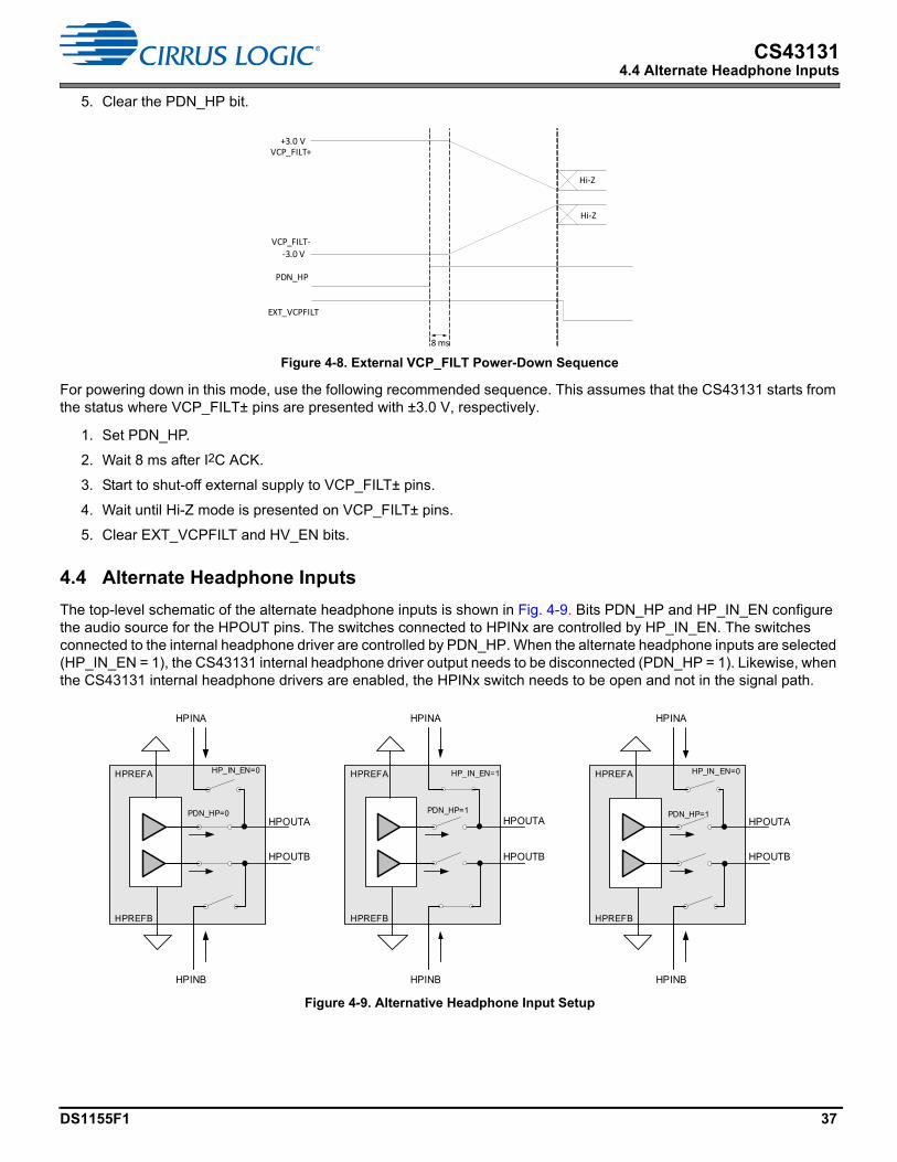
DS1155F1 37
CS431314.4 Alternate Headphone Inputs
5. Clear the PDN_HP bit.
Figure 4-8. External VCP_FILT Power-Down Sequence
For powering down in this mode, use the following recommended sequence. This assumes that the CS43131 starts from the status where VCP_FILT± pins are presented with ±3.0 V, respectively.
1. Set PDN_HP.
2. Wait 8 ms after I2C ACK.
3. Start to shut-off external supply to VCP_FILT± pins.
4. Wait until Hi-Z mode is presented on VCP_FILT± pins.
5. Clear EXT_VCPFILT and HV_EN bits.
4.4 Alternate Headphone Inputs
The top-level schematic of the alternate headphone inputs is shown in Fig. 4-9. Bits PDN_HP and HP_IN_EN configure the audio source for the HPOUT pins. The switches connected to HPINx are controlled by HP_IN_EN. The switches connected to the internal headphone driver are controlled by PDN_HP. When the alternate headphone inputs are selected (HP_IN_EN = 1), the CS43131 internal headphone driver output needs to be disconnected (PDN_HP = 1). Likewise, when the CS43131 internal headphone drivers are enabled, the HPINx switch needs to be open and not in the signal path.
Figure 4-9. Alternative Headphone Input Setup
EXT_VCPFILT
PDN_HP
VCP_FILT+
VCP_FILT‐
8 ms
+3.0 V
‐3.0 V
Hi‐Z
Hi‐Z
HPREFB
HPOUTA
HPOUTB
HPINA
HPINB
HPREFA
HPREFB
HPOUTA
HPOUTB
HPINA
HPINB
HPREFA
PDN_HP=0
HP_IN_EN=0
PDN_HP=1
HP_IN_EN=1
HPREFB
HPOUTA
HPOUTB
HPINA
HPINB
HPREFA
PDN_HP=1
HP_IN_EN=0
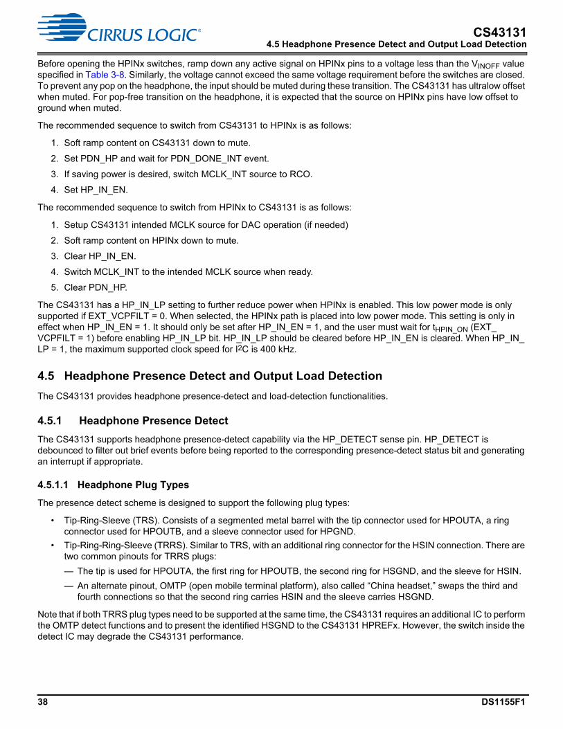
38 DS1155F1
CS431314.5 Headphone Presence Detect and Output Load Detection
Before opening the HPINx switches, ramp down any active signal on HPINx pins to a voltage less than the VINOFF value specified in Table 3-8. Similarly, the voltage cannot exceed the same voltage requirement before the switches are closed. To prevent any pop on the headphone, the input should be muted during these transition. The CS43131 has ultralow offset when muted. For pop-free transition on the headphone, it is expected that the source on HPINx pins have low offset to ground when muted.
The recommended sequence to switch from CS43131 to HPINx is as follows:
1. Soft ramp content on CS43131 down to mute.
2. Set PDN_HP and wait for PDN_DONE_INT event.
3. If saving power is desired, switch MCLK_INT source to RCO.
4. Set HP_IN_EN.
The recommended sequence to switch from HPINx to CS43131 is as follows:
1. Setup CS43131 intended MCLK source for DAC operation (if needed)
2. Soft ramp content on HPINx down to mute.
3. Clear HP_IN_EN.
4. Switch MCLK_INT to the intended MCLK source when ready.
5. Clear PDN_HP.
The CS43131 has a HP_IN_LP setting to further reduce power when HPINx is enabled. This low power mode is only supported if EXT_VCPFILT = 0. When selected, the HPINx path is placed into low power mode. This setting is only in effect when HP_IN_EN = 1. It should only be set after HP_IN_EN = 1, and the user must wait for tHPIN_ON (EXT_VCPFILT = 1) before enabling HP_IN_LP bit. HP_IN_LP should be cleared before HP_IN_EN is cleared. When HP_IN_LP = 1, the maximum supported clock speed for I2C is 400 kHz.
4.5 Headphone Presence Detect and Output Load Detection
The CS43131 provides headphone presence-detect and load-detection functionalities.
4.5.1 Headphone Presence Detect
The CS43131 supports headphone presence-detect capability via the HP_DETECT sense pin. HP_DETECT is debounced to filter out brief events before being reported to the corresponding presence-detect status bit and generating an interrupt if appropriate.
4.5.1.1 Headphone Plug Types
The presence detect scheme is designed to support the following plug types:
• Tip-Ring-Sleeve (TRS). Consists of a segmented metal barrel with the tip connector used for HPOUTA, a ring connector used for HPOUTB, and a sleeve connector used for HPGND.
• Tip-Ring-Ring-Sleeve (TRRS). Similar to TRS, with an additional ring connector for the HSIN connection. There are two common pinouts for TRRS plugs:
— The tip is used for HPOUTA, the first ring for HPOUTB, the second ring for HSGND, and the sleeve for HSIN.
— An alternate pinout, OMTP (open mobile terminal platform), also called “China headset,” swaps the third and fourth connections so that the second ring carries HSIN and the sleeve carries HSGND.
Note that if both TRRS plug types need to be supported at the same time, the CS43131 requires an additional IC to perform the OMTP detect functions and to present the identified HSGND to the CS43131 HPREFx. However, the switch inside the detect IC may degrade the CS43131 performance.

DS1155F1 39
CS431314.5 Headphone Presence Detect and Output Load Detection
4.5.1.2 Headphone Detect Methods
CS43131 can detect the presence or absence of a plug. For a headphone-presence detect, a sense pin is connected to a terminal on the receptacle such that, if no plug is inserted, the pin is floating. If a plug is inserted, the pin is shorted to the tip (T) terminal. The presence detect function is accomplished by having a small current source inside the CS43131 to pull up the pin if it is left floating (no plug). If a plug is inserted and the sense pin is shorted to HPOUTA, when HP amp is powered down, it is assumed that the sense pin is pulled low via clamps at the HP amp output. If the HP amp is running, the sense pin is shorted to the output signal and, therefore, is pulled below a certain threshold via the output stage of the HP amp. Thus, a low level at the sense pin indicates plug inserted, and a high level at the sense pin indicates plug removed.
4.5.1.3 Headphone Detect Registers
This section describes the behavior and interaction of the headphone-detect debounce register fields. See Fig. 4-10 for reference.
Figure 4-10. Headphone Detect Block Diagram
• HPDETECT_CTRL configures the operation of the HP detect circuit.
• HPDETECT_INV inverts the signal from the HP detect circuit.
• HPDETECT_FALL_DBC_TIME configures the HP_DETECT falling debounce time.
• HPDETECT_RISE_DBC_TIME configures the HP_DETECT rising debounce time.
• HPDETECT_PLUG_DBC shows the falling-edge-debounced version of HP_DETECT signal.
• HPDETECT_UNPLUG_DBC shows the rising-edge-debounced version of HP_DETECT signal.
• HPDETECT_PLUG_INT shows the headphone plug-in event status.
• HPDETECT_UNPLUG_INT shows the headphone unplug event status.
• HPDETECT_PLUG_INT_MASK is the interrupt mask of headphone plug-in event status.
• HPDETECT_UNPLUG_INT_MASK is the interrupt mask of headphone unplug event status.
4.5.1.4 Headphone Detect and Interrupts Setup Instructions
The following steps are required for activation of headphone-detect debounce interrupt status:
1. Ensure the I2C is ready to respond to control port command.
2. Clear the interrupt masks.
3. Write to HPDETECT_RISE_DBC_TIME and HPDETECT_FALL_DBC_TIME (see p. 131) to enable debounce for presence detect plug/unplug.
4. Set HPDETECT_CTRL to 11 to enable the HPDETECT functions.
HP_DETECT0
1
HP Detect Block
No Delay
HP DetectPlug/Unplug
Detect
HP Detect Plug/Unplug Interrupt
Mask
HP DetectPlug/Unplug Interrupt
Status
Interrupt Handler Block
INT
Read Clears INT
FALL_DEBOUNCE
RISE DEBOUNCE
No Delay
HP DetectDebounced Status
HPDETECT_CTRL p. 131
HPDETECT_PLUG_INT p. 134HPDETECT_UNPLUG_INT p. 134
HPDETECT_RISE_DBC_TIME p. 131
HPDETECT_FALL_DBC_TIME p. 131
HPDETECT_INV p. 131
HPDETECT_PLUG_DBC p. 131HPDETECT_UNPLUG_DBC p. 132
HPDETECT_PLUG_INT_MASK p. 137HPDETECT_UNPLUG_INT_MASK p. 137

40 DS1155F1
CS431314.5 Headphone Presence Detect and Output Load Detection
The interrupt status bits can be found in Section 7.6.1.
4.5.2 HP Load Detection
The CS43131 can measure the impedance of headphone DC load. Before taking measurements, the following criteria must be met:
• The CS43131 is out of reset.
• XTAL is powered on, an external MCLK is provided or PLL mode is used to generate internal MCLK. MCLK_INT is properly configured.
• The headphone output is powered down (PDN_HP = 1).
• The alternate headphone input is powered down (HP_IN_EN = 0).
• HPDETECT is high to indicate a headphone is plugged in.
• The HPLOAD_EN bit is set to turn on the impedance measurement subsystem. HPLOAD_ON_INT is unmasked and there has been a long enough wait to confirm the subsystem is properly started.
• The HPLOAD_DC_DONE interrupt is unmasked.
Either Channel A or Channel B to be measured by setting HPLOAD_CHN_SEL. The measurement process by clearing and setting the HPLOAD_DC_START bit. Once started, HPLOAD_DC_BUSY bit is set and a slowly ramping voltage is asserted on the headphone load for a maximum of 200 ms, then holds constant for 100 ms. Fig. 4-11 shows the a waveform of the impedance detection voltage.
Figure 4-11. Impedance Detection Voltage
Upon measurement completion, the following occurs:
1. The voltage asserted ramps down for 200 ms and is then removed.
2. The result of the measured resistance is reported in RL_DC_STAT.
3. HPLOAD_DC_DONE bit is set and the interrupt is triggered.
4. If HPLOAD_DC_ONCE bit has not been set, it is set. This bit is sticky until an HP unplug event has happened.
Once interrupted, the application processor services the interrupt by reading HPLOAD_DC_DONE_INT. At this point, another measurement process can be initiated by clearing and setting the HPLOAD_DC_START bit. The impedance measurement subsystem can also be turned off by clearing the HPLOAD_EN bit. HPLOAD_EN must be cleared (and confirmed by unmasked HPLOAD_OFF_INT) before enabling the headphone output or the alternate headphone input.
During the impedance measurement process, the following conditions trigger the error interrupt bits:
• The headphone load is not present or is unplugged before the impedance measurement is complete (HPLOAD_UNPLUG_INT).
• The headphone load is out of range, as specified in Table 3-7 (HPLOAD_OOR_INT).
• The headphone load measurement process is started without HP being properly turned off (HPLOAD_HPON_INT).
• The AC headphone load measurement process is initiated before the HPLOAD_DC_ONCE bit is set (HPLOAD_NO_DC_INT).
Time
Voltage
200 ms
100 ms
200 ms
DS1155F1 41
CS431314.6 Clocking Architecture
The HPLOAD error interrupt bits are sticky. If any HPLOAD error interrupt bits are flagged, the RL_DC_STAT value should be treated as invalid.
4.5.2.1 AC Load Detection
The CS43131 can also measure the headphone load impedance in the frequency range of 20 Hz to 20 kHz. The required conditions before the measurement is similar to the low frequency load measurement, with one exception—HPLOAD_MEAS_FREQ is set at the frequency of interest. Refer to Section 7.5.14 and Section 7.5.15 for details.
After HPLOAD_AC_START bit is cleared and set:
1. HPLOAD_AC_BUSY bit is set
2. The result of the measured resistance is reported in RL_AC_STAT.
3. HPLOAD_AC_DONE_INT is set and the interrupt is triggered.
For each headphone, the low-frequency load measurement must be performed (as indicated by the HPLOAD_DC_ONCE bit) before any impedance is measured at other frequencies. If the low-frequency load measurement is not performed and the process is initiated by pulsing the HPLOAD_AC_START bit low and high, the CS43131 can not generate a test signal and sets the HPLOAD_NO_DC_INT error interrupt bit. Any RL_AC_STAT value should be treated as invalid.
Once the measurement begins, a tone at the specified frequency is applied on the headphone load. Because the test tone is in the audio frequency range, it can be audible by the headphone user. It is recommended that the user system notify the headphone user of the expected events before initiating this measurement.
For each frequency, the measurement completion time is affected by the frequency of interest. The lower the frequency, the longer the measurement time. For the relationship between the frequency under test and the measurement time, the following applies:
• For frequencies under test less than 6 kHz or when the CS43131 comes out of reset, 10 periods of the test tone is the measurement time.
• For frequencies under test between 6 and 13 kHz, 20 periods of the test tone is the measurement time.
• For frequencies under test between 13 and 20 kHz, 30 periods of the test tone is the measurement time.
See Section 5.14.2 for example code of AC impedance measurement.
4.6 Clocking Architecture
4.6.1 Master Clock (MCLK) Sources
The MCLK is required by the CS43131 to operate any functionality associated with control, serial-port operation, or data conversion. Depending on the setting of MCLK_SRC_SEL (see p. 114), the MCLK can be provided by one of following methods:
• Sourced from a crystal oscillator between XTI/MCLK and XTO pins (see Fig. 4-12), then used directly as MCLK_INT
• Externally sourced through the XTI/MCLK input pin (see Fig. 4-13)
• PLL reference clock is provided through the XTI/MCLK input pin (see Fig. 4-13), then use internal PLL to convert into MCLK_INT
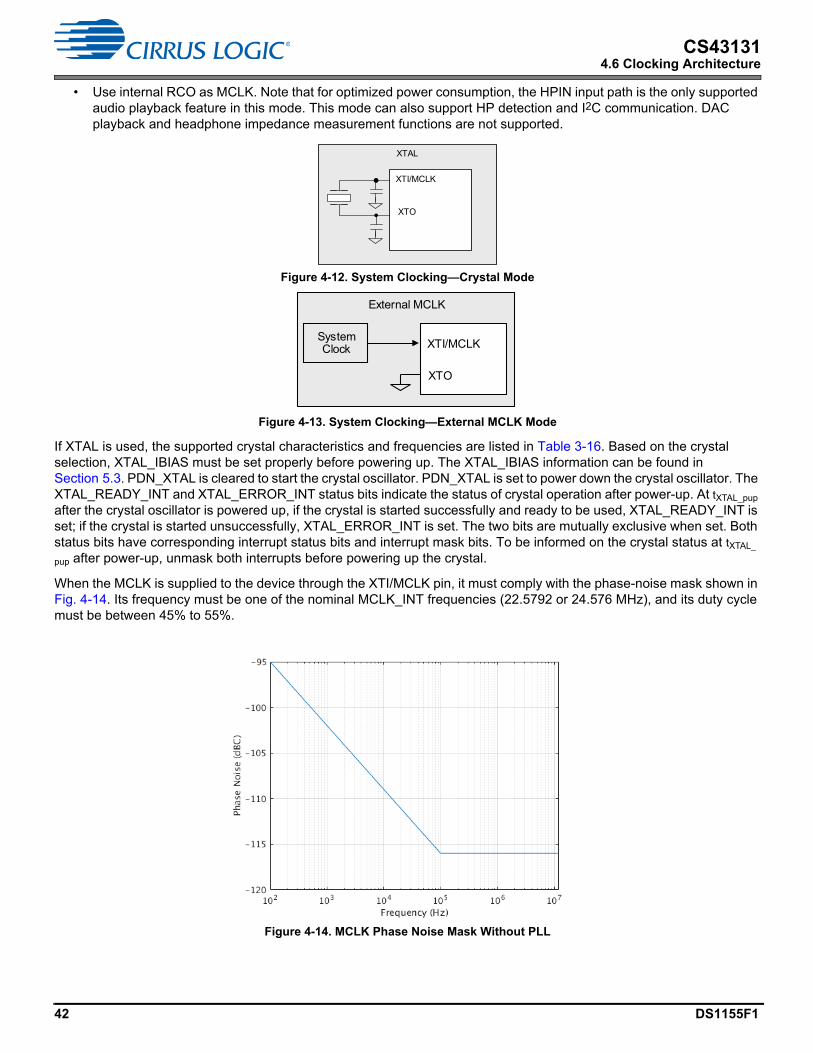
42 DS1155F1
CS431314.6 Clocking Architecture
• Use internal RCO as MCLK. Note that for optimized power consumption, the HPIN input path is the only supported audio playback feature in this mode. This mode can also support HP detection and I2C communication. DAC playback and headphone impedance measurement functions are not supported.
Figure 4-12. System Clocking—Crystal Mode
Figure 4-13. System Clocking—External MCLK Mode
If XTAL is used, the supported crystal characteristics and frequencies are listed in Table 3-16. Based on the crystal selection, XTAL_IBIAS must be set properly before powering up. The XTAL_IBIAS information can be found in Section 5.3. PDN_XTAL is cleared to start the crystal oscillator. PDN_XTAL is set to power down the crystal oscillator. The XTAL_READY_INT and XTAL_ERROR_INT status bits indicate the status of crystal operation after power-up. At tXTAL_pup after the crystal oscillator is powered up, if the crystal is started successfully and ready to be used, XTAL_READY_INT is set; if the crystal is started unsuccessfully, XTAL_ERROR_INT is set. The two bits are mutually exclusive when set. Both status bits have corresponding interrupt status bits and interrupt mask bits. To be informed on the crystal status at tXTAL_
pup after power-up, unmask both interrupts before powering up the crystal.
When the MCLK is supplied to the device through the XTI/MCLK pin, it must comply with the phase-noise mask shown in Fig. 4-14. Its frequency must be one of the nominal MCLK_INT frequencies (22.5792 or 24.576 MHz), and its duty cycle must be between 45% to 55%.
Figure 4-14. MCLK Phase Noise Mask Without PLL
XTAL
XTI/MCLK
XTO
External MCLK
System Clock XTI/MCLK
XTO
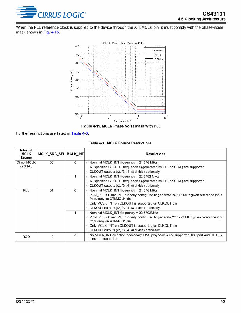
DS1155F1 43
CS431314.6 Clocking Architecture
When the PLL reference clock is supplied to the device through the XTI/MCLK pin, it must comply with the phase-noise mask shown in Fig. 4-15.
Figure 4-15. MCLK Phase Noise Mask With PLL
Further restrictions are listed in Table 4-3.
Table 4-3. MCLK Source Restrictions
Internal MCLK Source
MCLK_SRC_SEL MCLK_INT Restrictions
Direct MCLK or XTAL
00 0 • Nominal MCLK_INT frequency = 24.576 MHz • All specified CLKOUT frequencies (generated by PLL or XTAL) are supported • CLKOUT outputs (/2, /3, /4, /8 divide) optionally
1 • Nominal MCLK_INT frequency = 22.5792 MHz • All specified CLKOUT frequencies (generated by PLL or XTAL) are supported • CLKOUT outputs (/2, /3, /4, /8 divide) optionally
PLL 01 0 • Nominal MCLK_INT frequency = 24.576 MHz • PDN_PLL = 0 and PLL properly configured to generate 24.576 MHz given reference input
frequency on XTI/MCLK pin • Only MCLK_INT on CLKOUT is supported on CLKOUT pin • CLKOUT outputs (/2, /3, /4, /8 divide) optionally
1 • Nominal MCLK_INT frequency = 22.5792MHz • PDN_PLL = 0 and PLL properly configured to generate 22.5792 MHz given reference input
frequency on XTI/MCLK pin • Only MCLK_INT on CLKOUT is supported on CLKOUT pin • CLKOUT outputs (/2, /3, /4, /8 divide) optionally
RCO 10X • No MCLK_INT selection necessary. DAC playback is not supported. I2C port and HPIN_x
pins are supported.

44 DS1155F1
CS431314.7 Clock Output and Fractional-N PLL
Figure 4-16. MCLK Source Switching
A source to MCLK_INT, either the XTAL (or external MCLK), PLL, or the RCO, must be provided as long as CS43131 is operating; otherwise, the CS43131 will enter a non-responsive state. The only way to recover from this non-responsive state is either through a reset or POR event. Switching MCLK sources during DAC operation causes audible artifacts, but does not put the device in an unrecoverable state. In an MCLK source-switching event, the destined clock source must be present and ready before switching occurs.
After POR or reset event, RCO is selected as default source of MCLK_INT.
4.6.1.1 Internal RC Oscillator
As described in Section 4.6.1, the CS43131 includes an internal RC oscillator that can be used as a clock source for peripheral circuit such as control port or charge pump.
4.7 Clock Output and Fractional-N PLL
The CS43131 clock output can be used as a master clock for other data-conversion or signal-processing components, which requires synchronous timing to the CS43131.
The CLKOUT output is enabled by clearing PDN_CLKOUT.
Figure 4-17. CLKOUT Source Selection
Once enabled, CLKOUT is generated either from the internal crystal oscillator output (when used) or from the integrated fractional-N PLL; it can be selected by CLKOUT_SEL. CLKOUT_DIV can be used to set /2, /3, /4, or /8 to divide the selected clock source to targeted frequency.
4.7.1 Fractional-N PLL
The CS43131 has an integrated fractional-N PLL to support the clocking requirements of various applications. This PLL can be enabled or disabled by clearing or setting PDN_PLL bit. The input reference clock for the PLL is signal on XTI/MCLK pin (crystal-generated or external-feed).
InternalPLL
XTI/MCLK Internal MCLK
CLKOUT÷
RCO
CLKOUT_SEL p. 118
PDN_PLL p. 115
MCLK_SRC_SEL
CLKOUT_DIV p. 118
MCLK_INT p. 114
XTI/MCLK
PLL_OUTCLKOUT÷
CLKOUT_DIV
CLKOUT_SEL p. 118
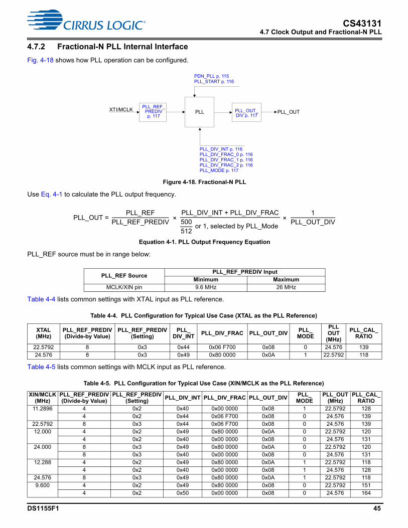
DS1155F1 45
CS431314.7 Clock Output and Fractional-N PLL
4.7.2 Fractional-N PLL Internal Interface
Fig. 4-18 shows how PLL operation can be configured.
Figure 4-18. Fractional-N PLL
Use Eq. 4-1 to calculate the PLL output frequency.
Equation 4-1. PLL Output Frequency Equation
PLL_REF source must be in range below:
Table 4-4 lists common settings with XTAL input as PLL reference.
Table 4-5 lists common settings with MCLK input as PLL reference.
PLL_REF SourcePLL_REF_PREDIV Input
Minimum MaximumMCLK/XIN pin 9.6 MHz 26 MHz
Table 4-4. PLL Configuration for Typical Use Case (XTAL as the PLL Reference)
XTAL (MHz)
PLL_REF_PREDIV (Divide-by Value)
PLL_REF_PREDIV (Setting)
PLL_DIV_INT
PLL_DIV_FRAC PLL_OUT_DIVPLL_MODE
PLL OUT
(MHz)
PLL_CAL_RATIO
22.5792 8 0x3 0x44 0x06 F700 0x08 0 24.576 13924.576 8 0x3 0x49 0x80 0000 0x0A 1 22.5792 118
Table 4-5. PLL Configuration for Typical Use Case (XIN/MCLK as the PLL Reference)
XIN/MCLK(MHz)
PLL_REF_PREDIV(Divide-by Value)
PLL_REF_PREDIV(Setting)
PLL_DIV_INT PLL_DIV_FRAC PLL_OUT_DIVPLL_MODE
PLL_OUT(MHz)
PLL_CAL_RATIO
11.2896 4 0x2 0x40 0x00 0000 0x08 1 22.5792 1284 0x2 0x44 0x06 F700 0x08 0 24.576 139
22.5792 8 0x3 0x44 0x06 F700 0x08 0 24.576 13912.000 4 0x2 0x49 0x80 0000 0x0A 0 22.5792 120
4 0x2 0x40 0x00 0000 0x08 0 24.576 13124.000 8 0x3 0x49 0x80 0000 0x0A 0 22.5792 120
8 0x3 0x40 0x00 0000 0x08 0 24.576 13112.288 4 0x2 0x49 0x80 0000 0x0A 1 22.5792 118
4 0x2 0x40 0x00 0000 0x08 1 24.576 12824.576 8 0x3 0x49 0x80 0000 0x0A 1 22.5792 1189.600 4 0x2 0x49 0x80 0000 0x08 0 22.5792 151
4 0x2 0x50 0x00 0000 0x08 0 24.576 164
PLLXTI/MCLK PLL_OUT
PLL_DIV_INT p. 116PLL_DIV_FRAC_0 p. 116PLL_DIV_FRAC_1 p. 116PLL_DIV_FRAC_2 p. 116PLL_MODE p. 117
PLL_REF_PREDIV p. 117
PDN_PLL p. 115PLL_START p. 116
PLL_OUT_DIV p. 117
PLL_OUT =PLL_REF
PLL_REF_PREDIV×
1PLL_OUT_DIV
PLL_DIV_INT + PLL_DIV_FRAC
or 1, selected by PLL_Mode×
500512
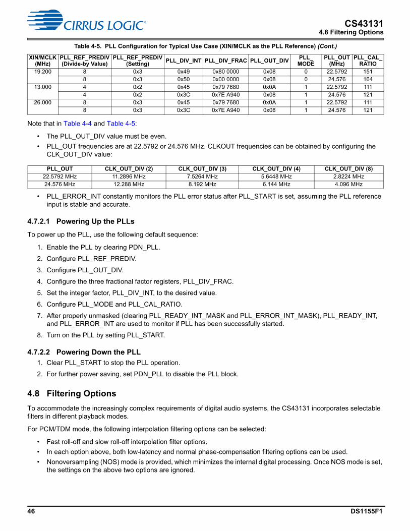
46 DS1155F1
CS431314.8 Filtering Options
Note that in Table 4-4 and Table 4-5:
• The PLL_OUT_DIV value must be even.
• PLL_OUT frequencies are at 22.5792 or 24.576 MHz. CLKOUT frequencies can be obtained by configuring the CLK_OUT_DIV value:
• PLL_ERROR_INT constantly monitors the PLL error status after PLL_START is set, assuming the PLL reference input is stable and accurate.
4.7.2.1 Powering Up the PLLs
To power up the PLL, use the following default sequence:
1. Enable the PLL by clearing PDN_PLL.
2. Configure PLL_REF_PREDIV.
3. Configure PLL_OUT_DIV.
4. Configure the three fractional factor registers, PLL_DIV_FRAC.
5. Set the integer factor, PLL_DIV_INT, to the desired value.
6. Configure PLL_MODE and PLL_CAL_RATIO.
7. After properly unmasked (clearing PLL_READY_INT_MASK and PLL_ERROR_INT_MASK), PLL_READY_INT, and PLL_ERROR_INT are used to monitor if PLL has been successfully started.
8. Turn on the PLL by setting PLL_START.
4.7.2.2 Powering Down the PLL
1. Clear PLL_START to stop the PLL operation.
2. For further power saving, set PDN_PLL to disable the PLL block.
4.8 Filtering Options
To accommodate the increasingly complex requirements of digital audio systems, the CS43131 incorporates selectable filters in different playback modes.
For PCM/TDM mode, the following interpolation filtering options can be selected:
• Fast roll-off and slow roll-off interpolation filter options.
• In each option above, both low-latency and normal phase-compensation filtering options can be used.
• Nonoversampling (NOS) mode is provided, which minimizes the internal digital processing. Once NOS mode is set, the settings on the above two options are ignored.
19.200 8 0x3 0x49 0x80 0000 0x08 0 22.5792 1518 0x3 0x50 0x00 0000 0x08 0 24.576 164
13.000 4 0x2 0x45 0x79 7680 0x0A 1 22.5792 1114 0x2 0x3C 0x7E A940 0x08 1 24.576 121
26.000 8 0x3 0x45 0x79 7680 0x0A 1 22.5792 1118 0x3 0x3C 0x7E A940 0x08 1 24.576 121
PLL_OUT CLK_OUT_DIV (2) CLK_OUT_DIV (3) CLK_OUT_DIV (4) CLK_OUT_DIV (8)22.5792 MHz 11.2896 MHz 7.5264 MHz 5.6448 MHz 2.8224 MHz24.576 MHz 12.288 MHz 8.192 MHz 6.144 MHz 4.096 MHz
Table 4-5. PLL Configuration for Typical Use Case (XIN/MCLK as the PLL Reference) (Cont.)
XIN/MCLK(MHz)
PLL_REF_PREDIV(Divide-by Value)
PLL_REF_PREDIV(Setting)
PLL_DIV_INT PLL_DIV_FRAC PLL_OUT_DIVPLL_MODE
PLL_OUT(MHz)
PLL_CAL_RATIO
DS1155F1 47
CS431314.9 Audio Serial Port (ASP)
The combination of the options results in five different filter combinations. The specifications for each filter can be found in Table 3-9, and response plots can be found in Section 9. These filters have been designed to accommodate a variety of musical tastes and styles. The PCM filter option register (see Section 7.5.2) is used to select filter options.
When in octuple-speed mode, the filter options above are not available and the internal digital processing is minimized. See the specification in Table 3-9 for filter characteristics.
The DSD processor mode uses a decimation-free DSD processing technique that allows for features such as matched PCM level output, DSD volume control, and 50-kHz on-chip filter.
4.9 Audio Serial Port (ASP)
The independent, highly configurable ASPs and auxiliary serial ports (XSPs) communicate audio data from other system devices, such as applications processors. Both ports can be configured to support common audio interfaces, TDM/I2S and left-justified (LJ).
ASP supports both PCM and DoP stream playback. XSP can only support DoP stream playback. For DAC playback, only one port needs to be enabled. Both ports are enabled only in specific application, such as PCM notification mixing with DSD/DoP content. Details regarding this application setup can be found in Section 4.12.
In this section, the reference to both ports is generalized as “xSP” to explain the common settings between the two ports.
4.9.1 Master and Slave Timing
Each serial port can operate as either the master of timing or as a slave to another device’s timing. If xSP_M/S is set, the serial port acts as a clock master. If xSP_M/S is cleared, the serial port acts as a clock slave.
• In Master Mode, xSP_SCLK and xSP_LRCK are outputs derived from the internal MCLK.
• In Slave Mode, xSP_SCLK and xSP_LRCK are inputs. Although the CS43131 does not generate the interface timings in Slave Mode, the expected LRCK and SCLK format must be programmed in the same way as in Master Mode (see Table 3-20).
• In both modes, the serial port sample rate register (xSP_SPRATE) must be set per audio content before enabling the serial port.
• When using ASP for PCM playback, the audio serial port sample bit size register (ASP_SPSIZE) must be set per audio content before enabling the ASP.
• When using XSP or ASP for DoP playback, the serial port sample bit size register (XSP_SPSIZE or ASP_SPSIZE) must be set per audio content before enabling the XSP or ASP. Note that the XSP_SPSIZE or ASP_SPSIZE must reflect the length of both DSD marker bits together with audio bits.
4.9.2 Power-Up, Power-Down, and Tristate
The xSP has separate power-down and tristate controls (PDN_xSP and xSP_3ST) for input data paths, which minimizes power consumption if the input port is not used. xSP master/slave operation is controlled only by the xSP_M/S setting, irrespective of the PDN_xSP and xSP_3ST settings.
• PDN_xSP. If a serial port’s SDIN functionality is not required, xSP can be powered down by setting PDN_xSP, which powers down the input data path and clocks of the serial port.
• xSP_3ST. In Master Mode, setting xSP_3ST tri-states the SCLK and LRCK clocks. Before setting an xSP_3ST bit, the associated serial port must be powered down and must not be powered up until the xSP_3ST bit is cleared. In Slave Mode, xSP_3ST does not affect the functionality of SCLK and LRCK clocks, given both pins are input pins.
4.9.3 I/O
The ASP port is associated with SDIN1, SCLK1, and LRCK1. The XSP port is associated with SDIN2, SCLK2, and LRCK2, which are shared with DSD interface:
• SCLKx—Serial data shift clock
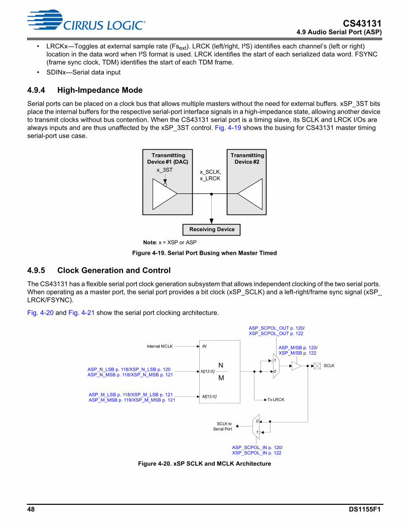
48 DS1155F1
CS431314.9 Audio Serial Port (ASP)
• LRCKx—Toggles at external sample rate (Fsext). LRCK (left/right, I²S) identifies each channel’s (left or right) location in the data word when I²S format is used. LRCK identifies the start of each serialized data word. FSYNC (frame sync clock, TDM) identifies the start of each TDM frame.
• SDINx—Serial data input
4.9.4 High-Impedance Mode
Serial ports can be placed on a clock bus that allows multiple masters without the need for external buffers. xSP_3ST bits place the internal buffers for the respective serial-port interface signals in a high-impedance state, allowing another device to transmit clocks without bus contention. When the CS43131 serial port is a timing slave, its SCLK and LRCK I/Os are always inputs and are thus unaffected by the xSP_3ST control. Fig. 4-19 shows the busing for CS43131 master timing serial-port use case.
Figure 4-19. Serial Port Busing when Master Timed
4.9.5 Clock Generation and Control
The CS43131 has a flexible serial port clock generation subsystem that allows independent clocking of the two serial ports. When operating as a master port, the serial port provides a bit clock (xSP_SCLK) and a left-right/frame sync signal (xSP_LRCK/FSYNC).
Fig. 4-20 and Fig. 4-21 show the serial port clocking architecture.
Figure 4-20. xSP SCLK and MCLK Architecture
Note: x = XSP or ASP
Transmitting Device #1 (DAC)
Transmitting Device #2
x_SCLK,x_LRCK
x_3ST
Receiving Device
N
M
Internal MCLK IN
N[13:0]
M[13:0]
SCLK0
1
0
1
To LRCK
SCLK to Serial Port
ASP_SCPOL_IN p. 120/XSP_SCPOL_IN p. 122
ASP_M/SB p. 120/XSP_M/SB p. 122
ASP_SCPOL_OUT p. 120/XSP_SCPOL_OUT p. 122
ASP_M_LSB p. 118/XSP_M_LSB p. 121ASP_M_MSB p. 119/XSP_M_MSB p. 121
ASP_N_LSB p. 118/XSP_N_LSB p. 120ASP_N_MSB p. 118/XSP_N_MSB p. 121
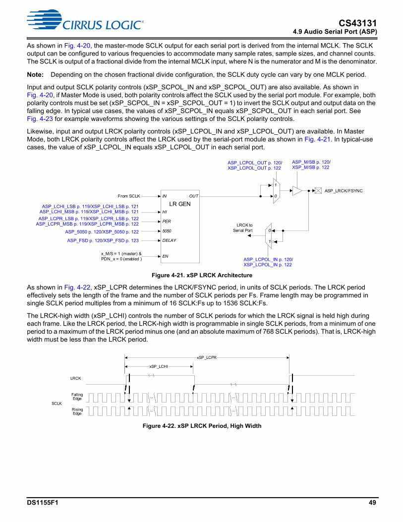
DS1155F1 49
CS431314.9 Audio Serial Port (ASP)
As shown in Fig. 4-20, the master-mode SCLK output for each serial port is derived from the internal MCLK. The SCLK output can be configured to various frequencies to accommodate many sample rates, sample sizes, and channel counts. The SCLK is output of a fractional divide from the internal MCLK input, where N is the numerator and M is the denominator.
Note: Depending on the chosen fractional divide configuration, the SCLK duty cycle can vary by one MCLK period.
Input and output SCLK polarity controls (xSP_SCPOL_IN and xSP_SCPOL_OUT) are also available. As shown in Fig. 4-20, if Master Mode is used, both polarity controls affect the SCLK used by the serial port module. For example, both polarity controls must be set (xSP_SCPOL_IN = xSP_SCPOL_OUT = 1) to invert the SCLK output and output data on the falling edge. In typical use cases, the values of xSP_SCPOL_IN equals xSP_SCPOL_OUT in each serial port. See Fig. 4-23 for example waveforms showing the various settings of the SCLK polarity controls.
Likewise, input and output LRCK polarity controls (xSP_LCPOL_IN and xSP_LCPOL_OUT) are available. In Master Mode, both LRCK polarity controls affect the LRCK used by the serial-port module as shown in Fig. 4-21. In typical-use cases, the value of xSP_LCPOL_IN equals xSP_LCPOL_OUT in each serial port.
Figure 4-21. xSP LRCK Architecture
As shown in Fig. 4-22, xSP_LCPR determines the LRCK/FSYNC period, in units of SCLK periods. The LRCK period effectively sets the length of the frame and the number of SCLK periods per Fs. Frame length may be programmed in single SCLK period multiples from a minimum of 16 SCLK:Fs up to 1536 SCLK:Fs.
The LRCK-high width (xSP_LCHI) controls the number of SCLK periods for which the LRCK signal is held high during each frame. Like the LRCK period, the LRCK-high width is programmable in single SCLK periods, from a minimum of one period to a maximum of the LRCK period minus one (and an absolute maximum of 768 SCLK periods). That is, LRCK-high width must be less than the LRCK period.
Figure 4-22. xSP LRCK Period, High Width
LRCK to Serial Port
ASP_LRCK/FSYNC0
1
0
1
IN
PER
OUT
HI
LR GEN
EN
From SCLK
x_M/S = 1 (master) &PDN_x = 0 (enabled )
5050
DELAY
ASP_5050 p. 120/XSP_5050 p. 122
ASP_FSD p. 120/XSP_FSD p. 123
ASP_LCPOL_IN p. 120/XSP_LCPOL_IN p. 122
ASP_M/SB p. 120/XSP_M/SB p. 122
ASP_LCPOL_OUT p. 120/XSP_LCPOL_OUT p. 122
ASP_LCHI_LSB p. 119/XSP_LCHI_LSB p. 121ASP_LCHI_MSB p. 119/XSP_LCHI_MSB p. 121
ASP_LCPR_LSB p. 119/XSP_LCPR_LSB p. 122ASP_LCPR_MSB p. 119/XSP_LCPR_MSB p. 122
SCLK
LRCK
Falling Edge
Rising Edge
xSP_LCPR
xSP_LCHI
...
...
...
...
...
...

50 DS1155F1
CS431314.9 Audio Serial Port (ASP)
As shown in Fig. 4-23, if Serial Port 50/50 Mode is enabled (xSP_5050 = 1), the LRCK high duration must be programmed to the LRCK period divided by two (rounded down to the nearest integer when the LRCK period is odd). When the serial port is in 50/50 Mode, setting the LRCK high duration to a value other than half of the period results in erroneous operation.
Figure 4-23. xSP_LRCK Period, High Width, 50/50 Mode
SCLK
LRCK
Falling Edge
Rising Edge
xSP_LCPR
xSP_LCHI
SCLK
LRCK
Falling Edge
Rising Edge
xSP_LCPR
xSP_LCHI
Even xSP _LCPR
Odd xSP _LCPR xSP_LCPR count clock is absent
xSP_LCHI
...
...
...
...
...
...
...
...
...
...
...
...
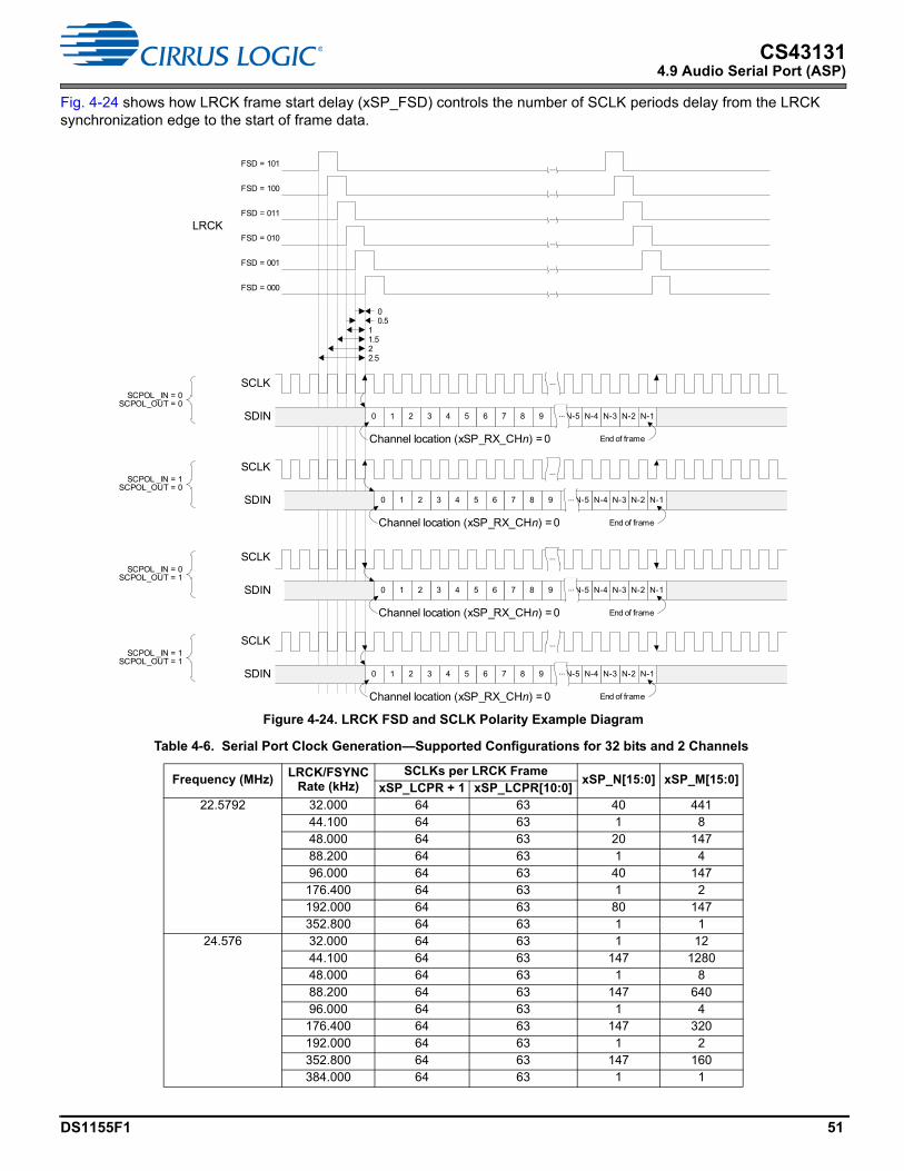
DS1155F1 51
CS431314.9 Audio Serial Port (ASP)
Fig. 4-24 shows how LRCK frame start delay (xSP_FSD) controls the number of SCLK periods delay from the LRCK synchronization edge to the start of frame data.
Figure 4-24. LRCK FSD and SCLK Polarity Example Diagram
Table 4-6. Serial Port Clock Generation—Supported Configurations for 32 bits and 2 Channels
Frequency (MHz)LRCK/FSYNC
Rate (kHz)SCLKs per LRCK Frame
xSP_N[15:0] xSP_M[15:0]xSP_LCPR + 1 xSP_LCPR[10:0]
22.5792 32.000 64 63 40 44144.100 64 63 1 848.000 64 63 20 14788.200 64 63 1 496.000 64 63 40 147176.400 64 63 1 2192.000 64 63 80 147352.800 64 63 1 1
24.576 32.000 64 63 1 1244.100 64 63 147 128048.000 64 63 1 888.200 64 63 147 64096.000 64 63 1 4176.400 64 63 147 320192.000 64 63 1 2352.800 64 63 147 160384.000 64 63 1 1
LRCK
0 1
Channel location (xSP_RX_CHn) = 0
FSD = 000
FSD = 001
FSD = 010
N-1N-2N-3N-4N-5
FSD = 011
0
FSD = 100
0.511.522.5
FSD = 101
End of frame
2 ...
...
...
...
...
...
...
3 4 5 6 7 8 9
...
...
0 1
Channel location (xSP_RX_CHn) = 0
N-1N-2N-3N-4N-5
End of frame
2 ...3 4 5 6 7 8 9
...
0 1
Channel location (xSP_RX_CHn) = 0
N-1N-2N-3N-4N-5
End of frame
2 ...3 4 5 6 7 8 9
0 1
Channel location (xSP_RX_CHn) = 0
N-1N-2N-3N-4N-5
End of frame
2 ...3 4 5 6 7 8 9
...SCLK
SDIN
SDIN
SCLK
SDIN
SCLK
SCLK
SDIN
SCPOL _IN = 0SCPOL_OUT = 0
SCPOL _IN = 1SCPOL_OUT = 0
SCPOL _IN = 0SCPOL_OUT = 1
SCPOL _IN = 1SCPOL_OUT = 1
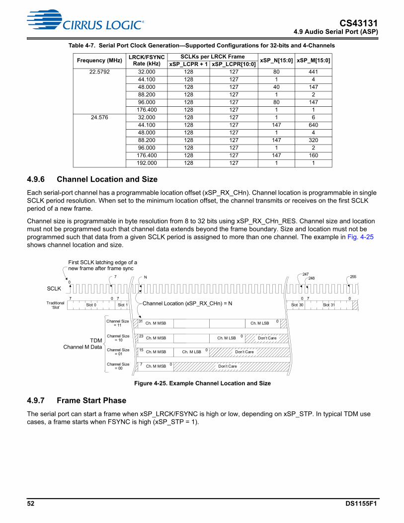
52 DS1155F1
CS431314.9 Audio Serial Port (ASP)
4.9.6 Channel Location and Size
Each serial-port channel has a programmable location offset (xSP_RX_CHn). Channel location is programmable in single SCLK period resolution. When set to the minimum location offset, the channel transmits or receives on the first SCLK period of a new frame.
Channel size is programmable in byte resolution from 8 to 32 bits using xSP_RX_CHn_RES. Channel size and location must not be programmed such that channel data extends beyond the frame boundary. Size and location must not be programmed such that data from a given SCLK period is assigned to more than one channel. The example in Fig. 4-25 shows channel location and size.
Figure 4-25. Example Channel Location and Size
4.9.7 Frame Start Phase
The serial port can start a frame when xSP_LRCK/FSYNC is high or low, depending on xSP_STP. In typical TDM use cases, a frame starts when FSYNC is high (xSP_STP = 1).
Table 4-7. Serial Port Clock Generation—Supported Configurations for 32-bits and 4-Channels
Frequency (MHz)LRCK/FSYNC
Rate (kHz)SCLKs per LRCK Frame
xSP_N[15:0] xSP_M[15:0]xSP_LCPR + 1 xSP_LCPR[10:0]
22.5792 32.000 128 127 80 44144.100 128 127 1 448.000 128 127 40 14788.200 128 127 1 296.000 128 127 80 147176.400 128 127 1 1
24.576 32.000 128 127 1 644.100 128 127 147 64048.000 128 127 1 488.200 128 127 147 32096.000 128 127 1 2176.400 128 127 147 160192.000 128 127 1 1
Slot 0
SCLK
Slot 1 Slot 30 Slot 31
0
247248 255
7 0 7 0 7 0
First SCLK latching edge of a new frame after frame sync
Traditional ‘Slot’
N
23 Ch. M MSB Ch. M LSB 0
15 Ch. M MSB Ch. M LSB 0
7 Ch. M MSB 0Channel Size = 00
Channel Size = 01
Channel Size = 10
Channel Location (xSP_RX_CHn) = N
TDM Channel M Data
Don’t Care
7
31 Ch. M MSB Ch. M LSB 0Channel Size = 11
Don’t Care
Don’t Care
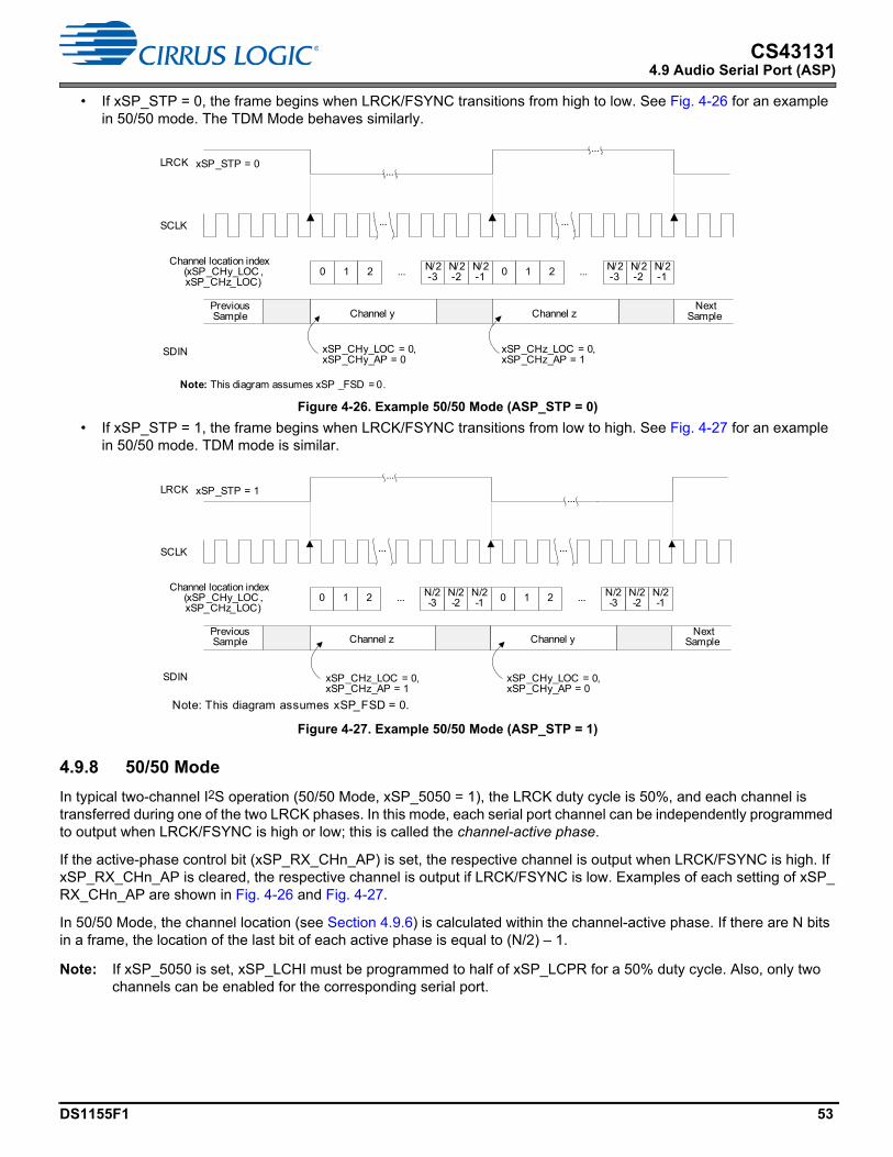
DS1155F1 53
CS431314.9 Audio Serial Port (ASP)
• If xSP_STP = 0, the frame begins when LRCK/FSYNC transitions from high to low. See Fig. 4-26 for an example in 50/50 mode. The TDM Mode behaves similarly.
Figure 4-26. Example 50/50 Mode (ASP_STP = 0)
• If xSP_STP = 1, the frame begins when LRCK/FSYNC transitions from low to high. See Fig. 4-27 for an example in 50/50 mode. TDM mode is similar.
Figure 4-27. Example 50/50 Mode (ASP_STP = 1)
4.9.8 50/50 Mode
In typical two-channel I2S operation (50/50 Mode, xSP_5050 = 1), the LRCK duty cycle is 50%, and each channel is transferred during one of the two LRCK phases. In this mode, each serial port channel can be independently programmed to output when LRCK/FSYNC is high or low; this is called the channel-active phase.
If the active-phase control bit (xSP_RX_CHn_AP) is set, the respective channel is output when LRCK/FSYNC is high. If xSP_RX_CHn_AP is cleared, the respective channel is output if LRCK/FSYNC is low. Examples of each setting of xSP_RX_CHn_AP are shown in Fig. 4-26 and Fig. 4-27.
In 50/50 Mode, the channel location (see Section 4.9.6) is calculated within the channel-active phase. If there are N bits in a frame, the location of the last bit of each active phase is equal to (N/2) – 1.
Note: If xSP_5050 is set, xSP_LCHI must be programmed to half of xSP_LCPR for a 50% duty cycle. Also, only two channels can be enabled for the corresponding serial port.
LRCK...
...
xSP_STP = 0
SCLK ... ...
Channel y Channel z
xSP_CHy_LOC = 0, xSP_CHy_AP = 0
xSP_CHz_LOC = 0, xSP_CHz_AP = 1
SDIN
Note: This diagram assumes xSP _FSD = 0.
Channel location index (xSP_CHy_LOC , xSP_CHz_LOC)
0 1 2 N/2-1
N/2-2
N/2-3... 0 1 2 N/2
-1N/2-2
N/2-3...
Next Sample
Previous Sample
LRCK
SCLK ... ...
Next Sample
Previous Sample
SDIN
...
...xSP_STP = 1
Channel location index (xSP_CHy_LOC , xSP_CHz_LOC)
0 1 2 N/2-1
N/2-2
N/2-3... 0 1 2 N/2
-1N/2-2
N/2-3...
Channel z
xSP_CHz_LOC = 0, xSP_CHz_AP = 1
Channel y
xSP_CHy_LOC = 0, xSP_CHy_AP = 0
Note: This diagram assumes xSP_FSD = 0.
54 DS1155F1
CS431314.9 Audio Serial Port (ASP)
4.9.9 Serial Port Status
Each serial port has five status bits. Each bit is sticky and must be read to be cleared. The status bits have associated mask bits to mask setting the INT pin when the status bit sets. A brief description of each status bit is shown in Table 4-8.
4.9.10 Serial Port Clock Pin Status
There are various control bits available that affect the output state of the serial port clock and data pins. Table 4-9 summarizes the possible states depending on these bit settings.
4.9.11 DoP (DSD over PCM) Mode
DoP is a protocol for packetizing DSD data into a PCM frame for transmission over an existing I2S interface. The ASP or XSP can accept DSD data in DoP format.
To use the DoP interface in Slave Mode, if MCLK_INT = 22.5792 MHz, the DoP interface clocks are required to be synchronous to MCLK_INT.
Table 4-8. Serial Port Status
Name Description Register Reference
Request Overload Set when too many input buffers request processing at the same time. If all channel size and location registers are properly configured to non-overlapping values, this error status must never set.
ASP_OVFL_INT p. 134XSP_OVFL_INT p. 135
LRCK Error Logical OR of LRCK early and LRCK late (see below). ASP_ERROR_INT p. 135XSP_ERROR_INT p. 135
LRCK Early Set when the number of SCLK periods per LRCK phase (high or low) is less than the expected count as determined by xSP_LCPR and xSP_LCHI.Note: The Rx LRCK early interrupt status is set during the first receive LRCK early event. Subsequent receive LRCK early events are not indicated until after valid LRCK transitions are detected.
ASP_EARLY_INT p. 135XSP_EARLY_INT p. 135
LRCK Late Set when the number of SCLK periods per LRCK phase (high or low) is greater than the expected count as determined by xSP_LCPR and xSP_LCHI.
ASP_LATE_INT p. 135XSP_LATE_INT p. 135
No LRCK Set when the number of SCLK periods counted exceeds twice the value of LRCK period (xSP_LCPR) without an LRCK edge.The Tx No LRCK interrupt status is set during the first instance of a no transmit LRCK condition. Subsequent no transmit LRCK conditions are not indicated until after valid LRCK transitions are detected.
ASP_NOLRCK_INT p. 135XSP_NOLRCK_INT p. 135
Table 4-9. xSP_SCLK and xSP_LRCK/FSYNC Pin States
xSP_3ST xSP_M/S PDN_xSPxSP_SCLKPin State
xSP_LRCK/FSYNCPin State
1 x x Hi-Z with weak pull-down Hi-Z with weak pull-down0 0 x Hi-Z with weak pull-down Hi-Z with weak pull-down0 1 0 Active Active0 1 1 Inactive Inactive 1
1.If xSP_LCPOL_OUT is set, xSP_LRCK/FSYNC inactive output is high. If xSP_LCPOL_OUT is cleared, xSP_LRCK/FSYNC inactive output is low.

DS1155F1 55
CS431314.10 DSD Interface
Each sample is 24 bits, as shown in Fig. 4-28, where the 8 most significant bits are used for the DSD marker and alternate with each sample between 0x05/0xFA. Each channel within a sample contains the same marker. The remaining 16 lower bits are then used for the DSD data, with the first or oldest bit in Slot t0.
Figure 4-28. DoP Data Sample and Stereo Stream Example
Each PCM frame is assigned to a specific channel (left or right), and when used for DSD streaming, each PCM frame contains only DSD data corresponding to its assigned channel. The CS43131 unpacks the received DoP data and reforms it into a DSD stream to feed the internal DSD data paths.
It includes the following features:
• 24 bits per PCM data sample
• I2S format is supported
• DoP data is unpacketed internally for DSD playback
• Clock Master and Slave Mode
• Up to 128•Fs DSD stream
— Accepts a 64•Fs DSD stream with [email protected] kHz
— Accepts a 128•Fs DSD stream with [email protected] kHz
To enable DoP interface on the ASP to take in DSD source:
1. Configure the ASP per clocking/format required by DoP content.
2. Configure DSD_SPEED per DoP content.
3. Set DSD_PRC_SRC = 10 and DSD_EN = 1.
4.10 DSD Interface
The DSD interface is enabled or disabled by PDN_DSDIF bit. When cleared, the DSD data interface is enabled. When using this interface, the DSD interface clock can be mastered by the CS43131 (DSD_M/SB=1). If set to Master Mode, DSDCLK toggles if both PDN_DSDIF and XSP_3ST bits are cleared, and DSD_EN is set.
If the DSD interface clock is slaved (DSD_M/SB=0), when MCLK_INT is set as 22.5792 MHz, DSDCLK is required to be synchronous to MCLK_INT. The DSDCLK can be derived by either:
• Exporting 1/2, 1/4, or 1/8 the frequency of the CS43131 crystal to CLKOUT, or
• Sourcing MCLK_INT and DSDCLK from the same external clock source
DSD Marker (8 MSB)
dm7 dm6 dm5 dm4 dm3 dm2 dm1 dm0 t0 t1 t2 t3 t4 t5 t6 t7 t8 t9 t10 t11 t12 t13 t14 t15
16 DSD Audio bits for one channel (oldest bit = t0)
24-Bit PCM FrameMSB LSB
0x050x05 0xFA 0xFA
LRCK (I2S)
SDATA (DoP) 0x05
Data Stream Example of Stereo DoP
DoP Data Sample
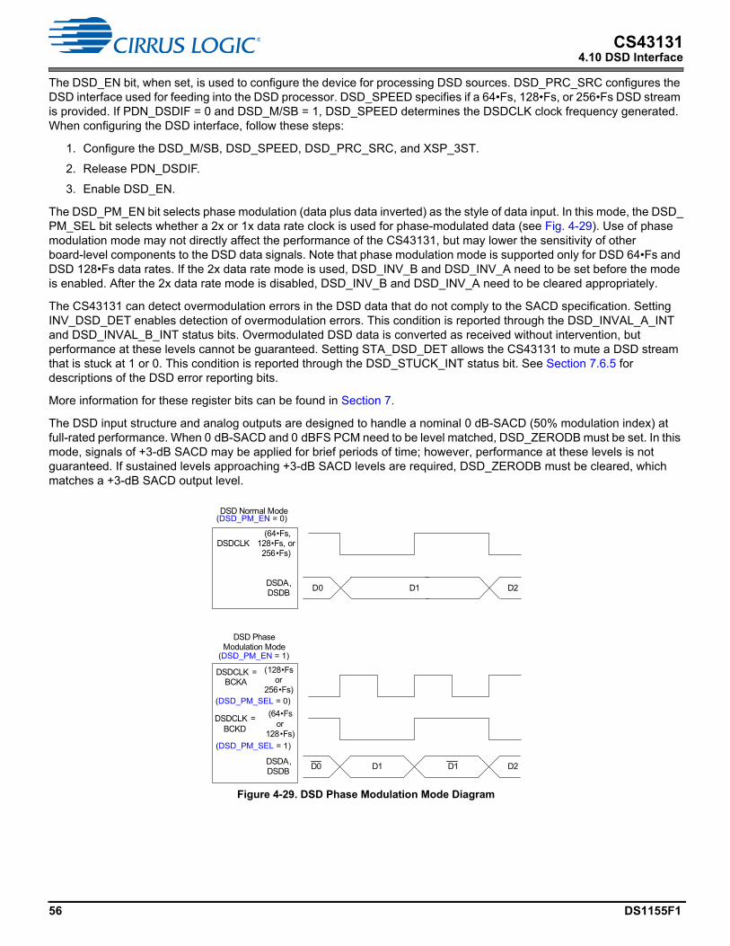
56 DS1155F1
CS431314.10 DSD Interface
The DSD_EN bit, when set, is used to configure the device for processing DSD sources. DSD_PRC_SRC configures the DSD interface used for feeding into the DSD processor. DSD_SPEED specifies if a 64•Fs, 128•Fs, or 256•Fs DSD stream is provided. If PDN_DSDIF = 0 and DSD_M/SB = 1, DSD_SPEED determines the DSDCLK clock frequency generated. When configuring the DSD interface, follow these steps:
1. Configure the DSD_M/SB, DSD_SPEED, DSD_PRC_SRC, and XSP_3ST.
2. Release PDN_DSDIF.
3. Enable DSD_EN.
The DSD_PM_EN bit selects phase modulation (data plus data inverted) as the style of data input. In this mode, the DSD_PM_SEL bit selects whether a 2x or 1x data rate clock is used for phase-modulated data (see Fig. 4-29). Use of phase modulation mode may not directly affect the performance of the CS43131, but may lower the sensitivity of other board-level components to the DSD data signals. Note that phase modulation mode is supported only for DSD 64•Fs and DSD 128•Fs data rates. If the 2x data rate mode is used, DSD_INV_B and DSD_INV_A need to be set before the mode is enabled. After the 2x data rate mode is disabled, DSD_INV_B and DSD_INV_A need to be cleared appropriately.
The CS43131 can detect overmodulation errors in the DSD data that do not comply to the SACD specification. Setting INV_DSD_DET enables detection of overmodulation errors. This condition is reported through the DSD_INVAL_A_INT and DSD_INVAL_B_INT status bits. Overmodulated DSD data is converted as received without intervention, but performance at these levels cannot be guaranteed. Setting STA_DSD_DET allows the CS43131 to mute a DSD stream that is stuck at 1 or 0. This condition is reported through the DSD_STUCK_INT status bit. See Section 7.6.5 for descriptions of the DSD error reporting bits.
More information for these register bits can be found in Section 7.
The DSD input structure and analog outputs are designed to handle a nominal 0 dB-SACD (50% modulation index) at full-rated performance. When 0 dB-SACD and 0 dBFS PCM need to be level matched, DSD_ZERODB must be set. In this mode, signals of +3-dB SACD may be applied for brief periods of time; however, performance at these levels is not guaranteed. If sustained levels approaching +3-dB SACD levels are required, DSD_ZERODB must be cleared, which matches a +3-dB SACD output level.
Figure 4-29. DSD Phase Modulation Mode Diagram
DSDA, DSDB
D1D0 D2
DSDCLK
DSD Normal Mode
(128•Fs or
256•Fs)
D1 D1 D2D0
DSDCLK =BCKD
DSDA, DSDB
(64•Fs or
128•Fs)
DSD Phase Modulation Mode
(64•Fs, 128•Fs, or 256•Fs)
DSDCLK =BCKA
(DSD_PM_EN = 0)
(DSD_PM_EN = 1)
(DSD_PM_SEL = 0)
(DSD_PM_SEL = 1)

DS1155F1 57
CS431314.11 DSD and PCM Mixing
4.11 DSD and PCM Mixing
For mobile application, the CS43131 provides a feature for mixing in PCM notification during DSD playback, with the setup in Table 4-10.
It is assumed that the DSD path has been properly configured for DSD playback.
During normal DSD playback, the ASP can be shut down. At the PCM notification event, the ASP must be properly configured to receive PCM samples at 44.1 kHz. After the ASP subclocks are running, set MIX_PCM_PREP to indicate to the CS43131 that the PCM mixing event is imminent. After 1.6 ms, MIX_PCM_DSD can be safely set to initiate the mixing process. After the PCM notification mixing is complete, clear both MIX_PCM_DSD and MIX_PCM_PREP at the same time. If desired, the ASP can be shut down to save power.
When mixing, use both PCM and DSD volume controls to attenuate the signal content on both paths (e.g., at least –6-dB attenuation on each) to avoid clipping on the mixing product. Use PCM_VOLUMEx to adjust the PCM path and DSD_VOLUMEx to adjust the DSD path. All the signal path settings apply to both path’s individual settings.
Figure 4-30. PCM and DSD Mixing Signal Flow
4.12 Standard Interrupts
The interrupt output pin, INT, is used to signal the occurrence of events within the device’s interrupt status registers. Events can be masked individually by setting corresponding bits in the interrupt mask registers. Table 4-11 lists interrupt status and mask registers. The configuration of mask bits determines which events cause the immediate assertion of INT:
• When an unmasked interrupt status event is detected, the status bit is set, and INT is asserted.
• When a masked interrupt status event is detected, the interrupt status bit is set, but INT is not affected.
Once INT is asserted, it remains asserted until all status bits that are unmasked and set have been read. Interrupt status bits are sticky and read-to-clear. Once set, they remain set until the register is read and the associated interrupt condition is not present. If a condition is still present and the status bit is read, although INT is deasserted, the status bit remains set.
To clear status bits set due to the initiation of a block, all interrupt status bits must be read after the corresponding module is enabled and before normal operation begins. Otherwise, unmasking these previously set status bits causes assertion of INT.
Interrupt source bits are set when edge-detect interrupts is detected, and they remain set until the register is read and the condition that caused the bit to assert is no longer present.
Table 4-10. Mixing Configurations Supported by the CS43131
PCM Input Configuration DSD Input ConfigurationI2S or TDM on
ASP44.1 kHz Master DSD on DSD IF 2.8224, 5.6448, or
11.2896 MHz on DSDCLK
MasterSlave 1
1.The ASP/XSP subclocks and DSDCLK are required to be synchronous.
Slave 1
Master DoP on XSP 176.4 or 352.8 kHz MasterSlave 1 Slave 1
DSD Processor
InterpolationFilter & Volume Control
DoP to DSD
Engine
MU
X
ASP
XSP/DSD Audio Interface
Multibit
ModulatorPCM
DSD
MIX_PCM_PREP p. 126MIX_PCM_DSD p. 126
PCM_VOLUME_B p. 128PCM_VOLUME_A p. 128
DSD_VOLUME_B p. 124DSD_VOLUME_A p. 125
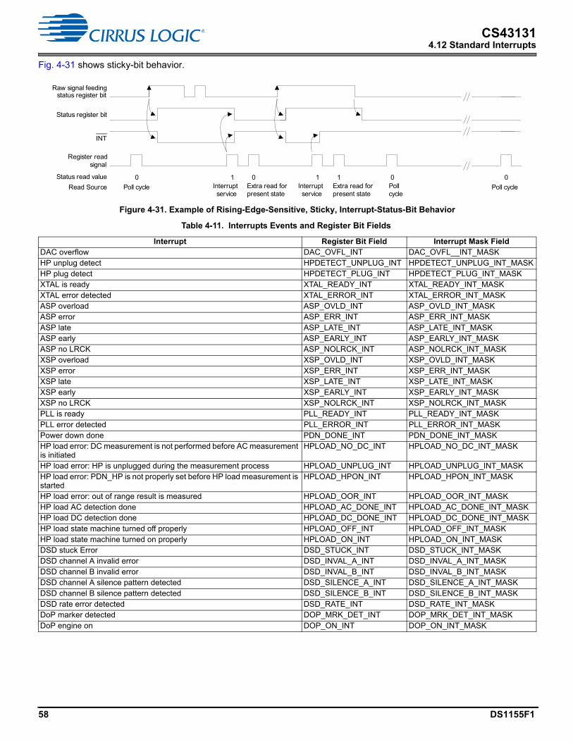
58 DS1155F1
CS431314.12 Standard Interrupts
Fig. 4-31 shows sticky-bit behavior.
Figure 4-31. Example of Rising-Edge-Sensitive, Sticky, Interrupt-Status-Bit Behavior
Table 4-11. Interrupts Events and Register Bit Fields
Interrupt Register Bit Field Interrupt Mask FieldDAC overflow DAC_OVFL_INT DAC_OVFL__INT_MASKHP unplug detect HPDETECT_UNPLUG_INT HPDETECT_UNPLUG_INT_MASKHP plug detect HPDETECT_PLUG_INT HPDETECT_PLUG_INT_MASKXTAL is ready XTAL_READY_INT XTAL_READY_INT_MASKXTAL error detected XTAL_ERROR_INT XTAL_ERROR_INT_MASKASP overload ASP_OVLD_INT ASP_OVLD_INT_MASKASP error ASP_ERR_INT ASP_ERR_INT_MASKASP late ASP_LATE_INT ASP_LATE_INT_MASKASP early ASP_EARLY_INT ASP_EARLY_INT_MASKASP no LRCK ASP_NOLRCK_INT ASP_NOLRCK_INT_MASKXSP overload XSP_OVLD_INT XSP_OVLD_INT_MASKXSP error XSP_ERR_INT XSP_ERR_INT_MASKXSP late XSP_LATE_INT XSP_LATE_INT_MASKXSP early XSP_EARLY_INT XSP_EARLY_INT_MASKXSP no LRCK XSP_NOLRCK_INT XSP_NOLRCK_INT_MASKPLL is ready PLL_READY_INT PLL_READY_INT_MASKPLL error detected PLL_ERROR_INT PLL_ERROR_INT_MASKPower down done PDN_DONE_INT PDN_DONE_INT_MASKHP load error: DC measurement is not performed before AC measurement is initiated
HPLOAD_NO_DC_INT HPLOAD_NO_DC_INT_MASK
HP load error: HP is unplugged during the measurement process HPLOAD_UNPLUG_INT HPLOAD_UNPLUG_INT_MASKHP load error: PDN_HP is not properly set before HP load measurement is started
HPLOAD_HPON_INT HPLOAD_HPON_INT_MASK
HP load error: out of range result is measured HPLOAD_OOR_INT HPLOAD_OOR_INT_MASKHP load AC detection done HPLOAD_AC_DONE_INT HPLOAD_AC_DONE_INT_MASKHP load DC detection done HPLOAD_DC_DONE_INT HPLOAD_DC_DONE_INT_MASKHP load state machine turned off properly HPLOAD_OFF_INT HPLOAD_OFF_INT_MASKHP load state machine turned on properly HPLOAD_ON_INT HPLOAD_ON_INT_MASKDSD stuck Error DSD_STUCK_INT DSD_STUCK_INT_MASKDSD channel A invalid error DSD_INVAL_A_INT DSD_INVAL_A_INT_MASKDSD channel B invalid error DSD_INVAL_B_INT DSD_INVAL_B_INT_MASKDSD channel A silence pattern detected DSD_SILENCE_A_INT DSD_SILENCE_A_INT_MASKDSD channel B silence pattern detected DSD_SILENCE_B_INT DSD_SILENCE_B_INT_MASKDSD rate error detected DSD_RATE_INT DSD_RATE_INT_MASKDoP marker detected DOP_MRK_DET_INT DOP_MRK_DET_INT_MASKDoP engine on DOP_ON_INT DOP_ON_INT_MASK
Raw signal feedingstatus register bit
Status register bit
___INT
Register readsignal
Status read value
Read Source
0 1 10 0 01
Poll cycle Interrupt service
Extra read forpresent state
Interrupt service
Extra read forpresent state
Poll cycle
Poll cycle

DS1155F1 59
CS431314.13 Control Port Operation
4.13 Control Port Operation
The control port is used to access control registers and on-chip memory locations, allowing the device to be configured for desired operational modes and formats. Control port operation may be completely asynchronous with respect to the audio sample rates. However, to avoid potential interference problems, control port pins must remain static if no operation is required.
The control port operates using a I2C interface with the CS43131 acting as a slave device. Device communication must not begin until tPUD (refer to Table 3-22) after power conditions are ready and RESET is released.
4.13.1 I2C Control Port Operation
The I2C control port operates completely asynchronously with the audio sample rates. However, to avoid interference problems, the I2C control-port pins must remain static if no operation is required.
The control-port uses the I2C interface, with the chip acting as a slave device. The I2C control port can operate in the following modes:
• Standard Mode (SM), with a bit rate of up to 100 kbit/s
• Fast Mode (FM), with a bit rate of up to 400 kbit/s
• Fast Mode Plus (FM+), with a bit rate of up to 1 Mbit/s
SDA is a bidirectional data line. Data is clocked into and out of the CS43131 by the SCL clock. Fig. 4-32, Fig. 4-33, and Fig. 4-34 show signal timings for read and write cycles. A Start condition is defined as a falling transition of SDA while SCL is high. A stop condition is defined as a rising transition of SDA while SCL is high. All other transitions of SDA must occur while SCL is low. Note that when HP_IN_LP is set, only SM and FM modes are supported.
To configure the last two bits of I2C address, CS43131 detects the ADR resistor connection type and measures the resistance upon a device power up (POR event) or after a hardware reset event (RESET deasserted). Based on the detected resistance, the I2C address is latched and cannot be changed until the next hardware reset event. The I2C address configuration is not ready until tPUD after the hardware reset event. During this period, the CS43131 does not respond to any user-issued I2C command. After configuration, the IC tristates the ADR pin and becomes high impedance internally to avoid a constant bias current.
To directly connect the ADR pin and ground, the last two bits of the I2C address are configured as the default 00. For the other options, use a resistor (with 5% accuracy) as suggested in the Table 4-12.
If the operation is a write, the 3 bytes after the chip address are the memory address pointer (MAP) that select the address of the register to be read or written to next. The byte following the MAP is the control byte. Bit[0] of the control byte, INCR, selects whether autoincrementing is to be used (INCR = 1), allowing successive reads or writes of consecutive registers. Bits[2:1] of the control byte indicate the size of the data for the autoincrement to be acted on. Table 4-13 explains the format for the I2C control byte.
Table 4-12. I2C Address Configurations
Connection Type Resistor Value () Last Two Bits of I2C AddressPull-up to VL 0 11Pull-up to VL 4990 10
Pull-down to GND 4990 01Pull-down to GND 0 00 (Default)
Table 4-13. I2C Control-Byte Format
Bit Name Description7:3 — Reserved
Default: 02:1 SIZE Register access width. Specifies the width of the register access.
00 8-bit (1 byte)01–11 Reserved

60 DS1155F1
CS431314.13 Control Port Operation
Each byte transferred on the I2C bus is separated by an acknowledge (ACK) bit. The CS43131 acknowledges each input byte read from the host, and the host must acknowledge each byte transmitted from the CS43131.
For write operations, the data bytes following the MAP byte are written to the CS43131 register addresses pointed to by the last received MAP address, plus however many autoincrements have occurred. Fig. 4-32 shows a write pattern with autoincrementing.
Figure 4-32. Control Port Timing, I2C Writes with Autoincrement (8-bit Data Access)
For read operations, the contents of the register pointed to by the last received MAP address (plus however many autoincrements have occurred if INCR was previously set) are output in the next byte. Fig. 4-33 shows a read pattern following the write pattern in Fig. 4-32. Notice how read addresses are based on the MAP bytes from Fig. 4-32.
Figure 4-33. Control Port Timing, I2C Reads with Autoincrement (8-Bit Data Access)
0 INCR Setting this bit allows the MAP address to autoincrement. The MAP address automatically increments every SIZE + 1 bytes accessed consecutively.
0 Disabled1 Enabled
Table 4-13. I2C Control-Byte Format (Cont.)
Bit Name Description
SCL
CHIP ADDRESS (WRITE)
MAP BYTE High (23:16)
START STOPACK
SDA
SDASource
Master Master Master
Pull-up Slave Slave Pull-up
ACK
R/W
= 0
Slave
AD
0A
D1
4 5 6 7 8 9 17 180 1 2 3
7 6 5 4 3 2 1 0
ACK
34
MAP BYTE Mid (15:8)
MAP BYTE Low (7:0)
36
ACK ACK
CONTROL BYTE
7 6 5 4 3 2 1 0
37 3835
INC
R =
1
SIZ
E =
00Empty
7 0 7 0 7 0
16 26 2725 39 40 41 42 43 44
7 0 7 0
45
DATA BYTE 1
DATA BYTE N
Master Master Master Master M
Slave Slave Slave Slave
MAP ADDRESS
MAP ADDRESS
+ (N–1)
ACK ACK
Addr = 01100
SCL
CHIP ADDRESS (READ)
START
SDA
SDASource
Master
Pull-up
Slave
Pull-up
ACK
R/W
= 1
AD
0A
D1
4 5 6 7 8 9 17 0 1 2 3
7 6 5 4 3 2 1 0
ACK NACK
7 0 7 0
16
DATA BYTE 1
DATA BYTE N
M MSlave
STOP
MAP ADDRESS
MAP ADDRESS
+ (N–1)
Addr = 01100
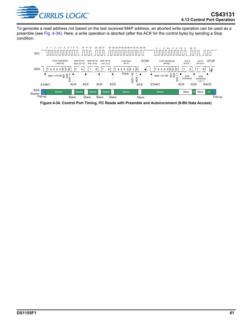
DS1155F1 61
CS431314.13 Control Port Operation
To generate a read address not based on the last received MAP address, an aborted write operation can be used as a preamble (see Fig. 4-34). Here, a write operation is aborted (after the ACK for the control byte) by sending a Stop condition.
Figure 4-34. Control Port Timing, I2C Reads with Preamble and Autoincrement (8-Bit Data Access)
SCL
CHIP ADDRESS (WRITE)
MAP BYTE High (23:16)
START
STOP
ACK
SDA
SDASource
Master Master Master
Pull-up Slave
Slave
Pull-up
ACK
R/W
= 0Addr = 01100
AD
0A
D1
4 5 6 7 8 9 17 180 1 2 3
7 6 5 4 3 2 1 0
ACK
34
MAP BYTE Mid (15:8)
MAP BYTE Low (7:0)
36
ACK ACK
CONTROL BYTE
7 6 5 4 3 2 1 0
37 3835
INC
R =
1
SIZ
E =
00Empty
7 0 7 0 7 0
16 26 2725 39 40 41 42 43 44
7 0 7 0
45
DATA BYTE 1
DATA BYTE N
Master Master
Slave Slave Slave
MSlave
START
R/W
= 1
AD
0A
D1
7 6 5 4 3 2 1 0
ACK ACK
M
NACK
STOP
Master
4 5 6 7 8 9 0 1 2 3 16 17
Slave
CHIP ADDRESS (READ)
MAP ADDRESS
MAP ADDRESS
+ (N-1)
Addr = 01100
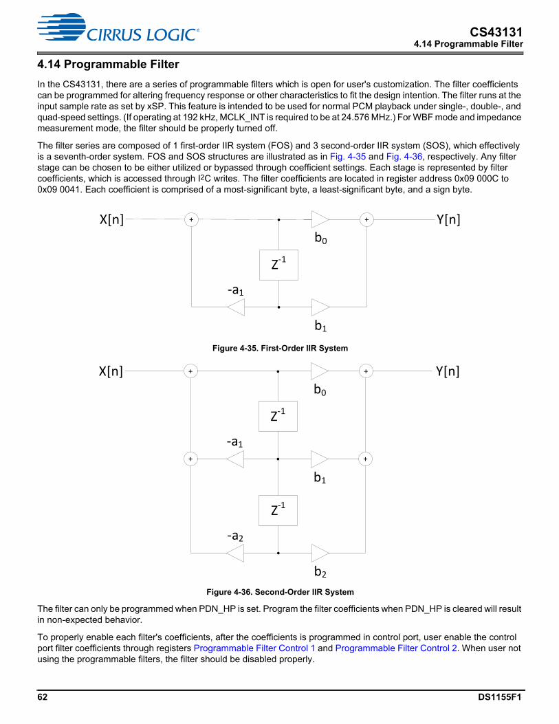
62 DS1155F1
CS431314.14 Programmable Filter
4.14 Programmable Filter
In the CS43131, there are a series of programmable filters which is open for user's customization. The filter coefficients can be programmed for altering frequency response or other characteristics to fit the design intention. The filter runs at the input sample rate as set by xSP. This feature is intended to be used for normal PCM playback under single-, double-, and quad-speed settings. (If operating at 192 kHz, MCLK_INT is required to be at 24.576 MHz.) For WBF mode and impedance measurement mode, the filter should be properly turned off.
The filter series are composed of 1 first-order IIR system (FOS) and 3 second-order IIR system (SOS), which effectively is a seventh-order system. FOS and SOS structures are illustrated as in Fig. 4-35 and Fig. 4-36, respectively. Any filter stage can be chosen to be either utilized or bypassed through coefficient settings. Each stage is represented by filter coefficients, which is accessed through I2C writes. The filter coefficients are located in register address 0x09 000C to 0x09 0041. Each coefficient is comprised of a most-significant byte, a least-significant byte, and a sign byte.
Figure 4-35. First-Order IIR System
Figure 4-36. Second-Order IIR System
The filter can only be programmed when PDN_HP is set. Program the filter coefficients when PDN_HP is cleared will result in non-expected behavior.
To properly enable each filter's coefficients, after the coefficients is programmed in control port, user enable the control port filter coefficients through registers Programmable Filter Control 1 and Programmable Filter Control 2. When user not using the programmable filters, the filter should be disabled properly.
Z‐1
b0
b1
‐a1
X[n] Y[n]+ +
Z‐1
X[n] Y[n]
Z‐1
+
+
+
‐a2
‐a1
b0
b1
b2
+

DS1155F1 63
CS431315 Applications
5 Applications
This section provides recommended application procedures and instruction sequences for standard CS43131 operations.
5.1 PLL Clocking
Data-path logic is in the MCLK_INT domain, where MCLK_INT is expected to be 22.5792 or 24.576 MHz. For clocking scenarios in which the external system MCLK provided to CS43131 is neither 22.5792 nor 24.576 MHz, the PLL must be turned on to provide the desired internal MCLK. At start up, the system uses RCO as the internal MCLK for PLL programming over I2C and switches to the PLL output after it settles. PLL start-up time is a maximum of 1 ms.
5.2 Power Sequencing
Note the following for power-up sequencing on the CS43131:
• VP must be powered up first.
• All other supplies can come up in any order before RESET is released.
Note the following for power-down sequencing on the CS43131:
• After RESET is asserted, VA/VCP/VL/VD can be removed in any order.
• VP must be powered down last.
5.3 Crystal Tuning
The CS43131 uses an external crystal as the source for internal MCLK. Refer to Table 3-16 for the load capacitance that is supported by CS43131. Table 5-1 lists supported crystals that meet the requirements for CS43131 and also shows also shows the XTAL_IBIAS settings for different crystals.
The crystal setting register (0x20052) must be set appropriately based on the crystal used.
The frequency at which the crystal eventually oscillates can be calculated using the formula below:
Fosc= 1/(2*π*sqrt[Lm*(Cm (C0+CL))/(Cm+C0+CL)]) ,
where
Lm = motional inductance of crystal
Cm = motional capacitance of crystal
C0 = shunt capacitance
CL = load capacitance
Trace capacitance and pad capacitance (approximately 0.5 pF) must also be taken into account while calculating the value of the load capacitors. Below are the steps to tune the crystal to the correct frequency:
1. Select load capacitor values that match the load capacitance spec in crystal manufacturer's data sheet.
Table 5-1. Example List of Supported Crystals
Manufacturer 1
1.Contact your local Cirrus Logic representative for a list of supported manufacturers and part numbers.
Part Number 1 Frequency (MHz)Bias Current Strength (µA)
Crystal Setting Register (0x20052)
River Electronics FCX-06-22.5792J51933 22.5792 12.5 0x04FCX-06-24.5760J51930 24.576 7.5 0x06
NDK NX2016SA 22.5792M EXS00A-CS09116 22.5792 15 0x02NX2016SA 24.576M EXS00A-CS09117 24.576
TXC 8Y22570001 22.5792 12.5 0x048Y24570001 24.576

64 DS1155F1
CS431315.4 Alert Mixing Shutdown
2. Power up and verify communication with CS43131. If there is no communication, it is possible that the crystal did not start. Check power rails and load capacitance and try again.
3. Clear PDN_CLKOUT in the Power Down Control (0x20000) register. This sets the clock output at MCLK_INT/2 frequency from CLKOUT pin.
4. Measure the frequency and verify that it is within acceptable range of the desired frequency. If yes, continue normal operation. If not, power down the chip, change the load capacitor values and go back to step 2.
Note: These steps need to be performed only once per PCB.
5.4 Alert Mixing Shutdown
To prevent a DSD mute pattern from turning off the DAC while mixing DSD data with PCM data, turn off the auto mute by clearing the DSD_AMUTE bit.
5.5 Enable/Disable Alternate Headphone Path (HPINx)
If the user decides to use the HPINx path, the following sequences must be followed to enable/disable the alternate headphone path (HPINx).
5.5.1 HPINx Alternate Headphone Path Enable Sequence
To enable the HPINx path, follow the sequence in Ex. 5-1.
5.5.2 HPINx Disable Sequence
To disable the HPINx path, follow the sequence in Ex. 5-2. For pop-free operation, the audio input must be completely ramped down before executing this sequence.
Example 5-1. HPINx Enable Sequence
TASK REGISTER/BIT FIELDS VALUE DESCRIPTION
Enable headphone input HP Output Control 1. 0x80000 0x38HP_CLAMPA HP_CLAMPB OUT_FSHP_IN_EN HP_IN_LP Reserved+1dB_EN
00111000
Function disabledFunction disabledHeadphone output voltage setting is irrelevantEnable HPIN switchFunction disabled
Wait for 1.1 ms.Enable low power mode HP Output Control 1. 0x80000 0x3C
HP_CLAMPA HP_CLAMPB OUT_FSHP_IN_EN HP_IN_LP Reserved+1dB_EN
00111100
Function disabledFunction disabledHeadphone output voltage setting is irrelevantEnable HPIN switchFunction enabled
Example 5-2. HPINx Disable
TASK REGISTER/BIT FIELDS VALUE DESCRIPTION
Disable HPINx low power mode
HP Output Control 1. 0x80000 0x38HP_CLAMPA HP_CLAMPB OUT_FSHP_IN_EN HP_IN_LP Reserved+1dB_EN
00111000
Function disabledFunction disabledHeadphone output voltage setting is irrelevantEnable HPIN switchFunction disabled
DS1155F1 65
CS431315.6 Headphone Power Down Sequences
5.6 Headphone Power Down Sequences
Examples of power down sequences for PCM and DSD are shown in Ex. 5-3 and Ex. 5-4, respectively. Follow the stated sequence every time to shut down the headphone output. The sequence assumes that the PDN_DONE_INT interrupt bit is unmasked.
5.6.1 PCM Power Down Sequence
5.6.2 DSD Power Down Sequence
Disable headphone input HP Output Control 1. 0x80000 0x30HP_CLAMPA HP_CLAMPB OUT_FSHP_IN_EN HP_IN_LP Reserved+1dB_EN
00110000
Disable HPIN
Example 5-3. PCM Power Down Sequence
STEP TASK REGISTER/BIT FIELDS VALUE DESCRIPTION
1 Enable PDN_DONE interrupt
Interrupt Mask 1. 0xF0010 data(0xF0010) AND (0xFE)
DAC_OVFL_INT_MASKHPDETECT_PLUG_INT_MASKHPDETECT_UNPLUG_INT_MASKXTAL_READY_INT_MASKXTAL_ERROR_INT_MASKPLL_READY_INT_MASKPLL_ERROR_INT_MASKPDN_DONE_INT_MASK
xxxxxxx0 Enable PDN_DONE interrupt
2 Power down amplifier Power Down Control. 0x20000 data(0x20000) OR (0x10)
PDN_XSPPDN_ASPPDN_DSDIFPDN_HPPDN_XTALPDN_PLLPDN_CLKOUTReserved
xxx1xxxx
Turn off HP
3 Wait for interrupt. Check for PDN_DONE_INT = 1 in Interrupt Status 1 register (0xF0000).4 Power down ASP Power Down Control. 0x20000 data(0x20000)
OR (0x40)PDN_XSPPDN_ASPPDN_DSDIFPDN_HPPDN_XTALPDN_PLLPDN_CLKOUTReserved
x1xxxxxx
Turn off ASP
Example 5-4. DSD Power Down Sequence
STEP TASK REGISTER/BIT FIELDS VALUE DESCRIPTION
1 Enable PDN_DONE interrupt
Interrupt Mask 1. 0xF0010 data(0xF0010) AND (0xFE)
DAC_OVFL_INT_MASKHPDETECT_PLUG_INT_MASKHPDETECT_UNPLUG_INT_MASKXTAL_READY_INT_MASKXTAL_ERROR_INT_MASKPLL_READY_INT_MASKPLL_ERROR_INT_MASKPDN_DONE_INT_MASK
xxxxxxx0 Enable PDN_DONE interrupt
Example 5-2. HPINx Disable (Cont.)
TASK REGISTER/BIT FIELDS VALUE DESCRIPTION

66 DS1155F1
CS431315.7 Headphone Power-Up Sequence
5.7 Headphone Power-Up Sequence
An example of the power-up sequence for PCM and DSD are shown in Ex. 5-5 and Ex. 5-6, respectively. Follow the stated sequence every time to power up the headphone output.
5.7.1 PCM Power-Up Sequence
2 Power down amplifier Power Down Control. 0x20000 data(0x20000) OR (0x10)
PDN_XSPPDN_ASPPDN_DSDIFPDN_HPPDN_XTALPDN_PLLPDN_CLKOUTReserved
xxx1xxxx
Turn off HP
3 Wait for interrupt. Check for PDN_DONE_INT = 1 in Interrupt Status 1 register (0xF0000).4 Power down XSP/ASP/
DSDIF interfacesPower Down Control. 0x20000 data(0x20000)
OR (0xE0)PDN_XSPPDN_ASPPDN_DSDIFPDN_HPPDN_XTALPDN_PLLPDN_CLKOUTReserved
111xxxxx
Example 5-5. PCM Power-Up Sequence
STEP TASK REGISTER/BIT FIELDS VALUE DESCRIPTION
1 Pop-free power-up settings 0x10010 0x990x80032 0x20
2 Power on appropriate interface.Power Down Control. 0x20000 data (0x20000) AND (0xBF)
PDN_XSPPDN_ASPPDN_DSDIFPDN_HPPDN_XTALPDN_PLLPDN_CLKOUTReserved
x0xxxxx0
Power up ASP
3 Power on amplifier Power Down Control. 0x20000 data (0x20000) AND (0xEF)
PDN_XSPPDN_ASPPDN_DSDIFPDN_HPPDN_XTALPDN_PLLPDN_CLKOUTReserved
xxx0xxx0
Power up HP
4 Wait for 12 ms5 Restore default settings 0x80032 0x00
0x10010 0x00
Example 5-4. DSD Power Down Sequence (Cont.)
STEP TASK REGISTER/BIT FIELDS VALUE DESCRIPTION
DS1155F1 67
CS431315.8 Power-Down Sequence in External VCPFILT Mode
5.7.2 DSD Power-Up Sequence
5.8 Power-Down Sequence in External VCPFILT Mode
These sequences allow the CS43131 to be powered down in external VCPFILT mode without any audible pops.
5.8.1 PCM Pop-Free Power-Down Sequence in External VCPFILT Mode
Example 5-6. DSD Power-Up Sequence
STEP TASK REGISTER/BIT FIELDS VALUE DESCRIPTION
1 Pop-free power-up settings 0x10010 0x990x80032 0x20
2 Power on appropriate interface.Power Down Control. 0x20000 data (0x20000) AND (0xHH)
For DoP on XSP, HH = 7F.For DoP on ASP, HH = BF.For DSD interface, HH = DF.
PDN_XSPPDN_ASPPDN_DSDIFPDN_HPPDN_XTALPDN_PLLPDN_CLKOUTReserved
BBBxxxxx
Enable XSP, ASP, or DSDIF interface
3 Power on amplifier Power Down Control. 0x20000 data (0x20000) AND (0xEF)
PDN_XSPPDN_ASPPDN_DSDIFPDN_HPPDN_XTALPDN_PLLPDN_CLKOUTReserved
xxx0xxx0
Power up HP
4 Wait for 12 ms5 Restore default settings 0x80032 0x00
0x10010 0x00
STEP TASK REGISTER/BIT FIELDS VALUE DESCRIPTION
1 Pop-free power-down settings 0x100100x80046
0x990x21
2 Mute both channels PCM Path Signal Control 1. 0x90003 data(0x90003) OR (0x03)
PCM_RAMP_DOWNPCM_VOL_BEQAPCM_SZCPCM_AMUTEPCM_AMUTEBEQAPCM_MUTE_APCM_MUTE_B
xxxxxx11
Channel A is mutedChannel B is muted
3 Wait 150 ms for mute to occur4 Enable PDN_DONE interrupt Interrupt Mask 1. 0xF0010 data(0xF0010)
AND (0xFE)DAC_OVFL_INT_MASKHPDETECT_PLUG_INT_MASKHPDETECT_UNPLUG_INT_MASKXTAL_READY_INT_MASKXTAL_ERROR_INT_MASKPLL_READY_INT_MASKPLL_ERROR_INT_MASKPDN_DONE_INT_MASK
xxxxxxx0 Enable PDN_DONE interrupt
5 Power down amplifier Power Down Control. 0x20000 data(0x20000) OR (0x10)
PDN_XSPPDN_ASPPDN_DSDIFPDN_HPPDN_XTALPDN_PLLPDN_CLKOUTReserved
xxx1xxxx
Turn off HP
6 Wait for interrupt. Check for PDN_DONE_INT = 1 in Interrupt Status 1 register (0xF0000).

68 DS1155F1
CS431315.8 Power-Down Sequence in External VCPFILT Mode
5.8.2 DSD Pop-Free Power-Down Sequence in External VCPFILT Mode
7 Power down ASP Power Down Control. 0x20000 data(0x20000) OR (0x40)
PDN_XSPPDN_ASPPDN_DSDIFPDN_HPPDN_XTALPDN_PLLPDN_CLKOUTReserved
x1xxxxxx
Turn off ASP
8 Unmute both channels PCM Path Signal Control 1. 0x90003 data(0x90003) AND (0xFC)
PCM_RAMP_DOWNPCM_VOL_BEQAPCM_SZCPCM_AMUTEPCM_AMUTEBEQAPCM_MUTE_APCM_MUTE_B
xxxxxx00
Channel A is unmutedChannel B is unmuted
9 Restore default settings 0x800460x10010
0x200x00
STEP TASK REGISTER/BIT FIELDS VALUE DESCRIPTION
1 Pop-free power-down settings 0x100100x80046
0x990x21
2 Mute both channels DSD Processor Path Signal Control 1. 0x70002
data(0x70002) OR (0x03)
DSD_RAMP_UPDSD_VOL_BEQADSD_SZCReservedDSD_AMUTEDSD_AMUTE_BEQADSD_MUTE_ADSD_MUTE_B
xxxxxx11
Channel A is mutedChannel B is muted
3 Wait 150 ms for mute to occur4 Enable PDN_DONE interrupt Interrupt Mask 1. 0xF0010 data(0xF0010)
AND (0xFE)DAC_OVFL_INT_MASKHPDETECT_PLUG_INT_MASKHPDETECT_UNPLUG_INT_MASKXTAL_READY_INT_MASKXTAL_ERROR_INT_MASKPLL_READY_INT_MASKPLL_ERROR_INT_MASKPDN_DONE_INT_MASK
xxxxxxx0 Enable PDN_DONE interrupt
5 Power down amplifier Power Down Control. 0x20000 data(0x20000) OR (0x10)
PDN_XSPPDN_ASPPDN_DSDIFPDN_HPPDN_XTALPDN_PLLPDN_CLKOUTReserved
xxx1xxxx
Turn off HP
6 Wait for interrupt. Check for PDN_DONE_INT = 1 in Interrupt Status 1 register (0xF0000).7 Power down XSP/ASP/DSDIF interfaces Power Down Control. 0x20000 data(0x20000)
OR (0xE0)PDN_XSPPDN_ASPPDN_DSDIFPDN_HPPDN_XTALPDN_PLLPDN_CLKOUTReserved
111xxxxx

DS1155F1 69
CS431315.9 Enabling and Disabling NOS Filter
5.9 Enabling and Disabling NOS Filter
Section 5.9.1 and Section 5.9.2 describe pop-free sequences for enabling and disabling the NOS filter, respectively.
5.9.1 Sequence for Enabling NOS Filter
8 Unmute both channels DSD Processor Path Signal Control 1. 0x70002
data(0x70002) AND (0xFC)
DSD_RAMP_UPDSD_VOL_BEQADSD_SZCReservedDSD_AMUTEDSD_AMUTE_BEQADSD_MUTE_ADSD_MUTE_B
xxxxxx00
Channel A is unmutedChannel B is unmuted
9 Restore default settings 0x800460x10010
0x200x00
STEP TASK REGISTER/BIT FIELDS VALUE DESCRIPTION
1 Set mute to occur with soft ramp only
PCM Path Signal Control 1. 0x90003 data (0x90003) AND (0xEF) OR
(0x20)PCM_RAMP_DOWNPCM_VOL_BEQAPCM_SZCPCM_AMUTEPCM_AMUTEBEQAPCM_MUTE_APCM_MUTE_B
xx
10xxxx
Enable soft ramp
2 Mute both channels PCM Path Signal Control 1. 0x90003 data (0x90003) OR (0x03)
PCM_RAMP_DOWNPCM_VOL_BEQAPCM_SZCPCM_AMUTEPCM_AMUTEBEQAPCM_MUTE_APCM_MUTE_B
xxxxxx11
Channel A output is mutedChannel B output is muted
3 Wait for 150 ms for mute to occur4 Enable NOS filter PCM Filter Option. 0x90000 data (0x90000)
OR (0x20)FILTER_SLOW_FASTBPHCOMP_LOWLATBNOSReservedPCM_WBF_ENHIGH_PASSDEEMP_ON
xx1
0 0xxx
NOS emulation mode is on
5 Restore PCM_SZC mode if desired
PCM Path Signal Control 1. 0x90003 0xHHPCM_RAMP_DOWNPCM_VOL_BEQAPCM_SZCPCM_AMUTEPCM_AMUTEBEQAPCM_MUTE_APCM_MUTE_B
xx
BBxxxx
Restore PCM_SZC to desired value
6 Unmute both channels PCM Path Signal Control 1. 0x90003 data (0x90003) AND (0xFC)
PCM_RAMP_DOWNPCM_VOL_BEQAPCM_SZCPCM_AMUTEPCM_AMUTEBEQAPCM_MUTE_APCM_MUTE_B
xxxxxx00
Function is disabledFunction is disabled
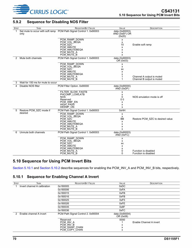
70 DS1155F1
CS431315.10 Sequence for Using PCM Invert Bits
5.9.2 Sequence for Disabling NOS Filter
5.10 Sequence for Using PCM Invert Bits
Section 5.10.1 and Section 5.10.2 describe sequences for enabling the PCM_INV_A and PCM_INV_B bits, respectively.
5.10.1 Sequence for Enabling Channel A Invert
STEP TASK REGISTER/BIT FIELDS VALUE DESCRIPTION
1 Set mute to occur with soft ramp only
PCM Path Signal Control 1. 0x90003 data (0x90003) AND (0xEF) OR
(0x20)PCM_RAMP_DOWNPCM_VOL_BEQAPCM_SZCPCM_AMUTEPCM_AMUTEBEQAPCM_MUTE_APCM_MUTE_B
xx
10xxxx
Enable soft ramp
2 Mute both channels PCM Path Signal Control 1. 0x90003 data (0x90003) OR (0x03)
PCM_RAMP_DOWNPCM_VOL_BEQAPCM_SZCPCM_AMUTEPCM_AMUTEBEQAPCM_MUTE_APCM_MUTE_B
xxxxxx11
Channel A output is mutedChannel B output is muted
3 Wait for 150 ms for mute to occur4 Disable NOS filter PCM Filter Option. 0x90000 data (0x90000)
AND (0xDF)FILTER_SLOW_FASTBPHCOMP_LOWLATBNOSReservedPCM_WBF_ENHIGH_PASSDEEMP_ON
xx0
0 0xxx
NOS emulation mode is off
5 Restore PCM_SZC mode if desired
PCM Path Signal Control 1. 0x90003 0xHHPCM_RAMP_DOWNPCM_VOL_BEQAPCM_SZCPCM_AMUTEPCM_AMUTEBEQAPCM_MUTE_APCM_MUTE_B
xx
BBxxxx
Restore PCM_SZC to desired value
6 Unmute both channels PCM Path Signal Control 1. 0x90003 data (0x90003) AND (0xFC)
PCM_RAMP_DOWNPCM_VOL_BEQAPCM_SZCPCM_AMUTEPCM_AMUTEBEQAPCM_MUTE_APCM_MUTE_B
xxxxxx00
Function is disabledFunction is disabled
STEP TASK REGISTER/BIT FIELDS VALUE DESCRIPTION
1 Invert channel A calibration 0x180005 0xDC0x180006 0xFA0x180015 0xFB0x180016 0xFB0x180025 0xF50x180026 0xFE0x180035 0x8F0x180036 0xFC
2 Enable channel A invert PCM Path Signal Control 2. 0x90004 data (0x90004) OR (0x08)
ReservedPCM_INV_APCM_INV_BPCM_SWAP_CHANPCM_COPY_CHAN
00001xxx
Enable Channel A invert
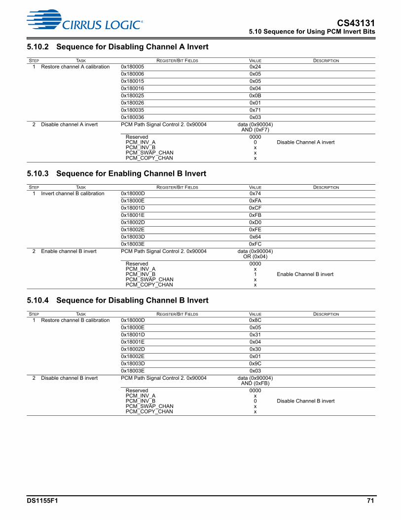
DS1155F1 71
CS431315.10 Sequence for Using PCM Invert Bits
5.10.2 Sequence for Disabling Channel A Invert
5.10.3 Sequence for Enabling Channel B Invert
5.10.4 Sequence for Disabling Channel B Invert
STEP TASK REGISTER/BIT FIELDS VALUE DESCRIPTION
1 Restore channel A calibration 0x180005 0x240x180006 0x050x180015 0x050x180016 0x040x180025 0x0B0x180026 0x010x180035 0x710x180036 0x03
2 Disable channel A invert PCM Path Signal Control 2. 0x90004 data (0x90004) AND (0xF7)
ReservedPCM_INV_APCM_INV_BPCM_SWAP_CHANPCM_COPY_CHAN
00000xxx
Disable Channel A invert
STEP TASK REGISTER/BIT FIELDS VALUE DESCRIPTION
1 Invert channel B calibration 0x18000D 0x740x18000E 0xFA0x18001D 0xCF0x18001E 0xFB0x18002D 0xD00x18002E 0xFE0x18003D 0x640x18003E 0xFC
2 Enable channel B invert PCM Path Signal Control 2. 0x90004 data (0x90004) OR (0x04)
ReservedPCM_INV_APCM_INV_BPCM_SWAP_CHANPCM_COPY_CHAN
0000x1xx
Enable Channel B invert
STEP TASK REGISTER/BIT FIELDS VALUE DESCRIPTION
1 Restore channel B calibration 0x18000D 0x8C0x18000E 0x050x18001D 0x310x18001E 0x040x18002D 0x300x18002E 0x010x18003D 0x9C0x18003E 0x03
2 Disable channel B invert PCM Path Signal Control 2. 0x90004 data (0x90004) AND (0xFB)
ReservedPCM_INV_APCM_INV_BPCM_SWAP_CHANPCM_COPY_CHAN
0000x0xx
Disable Channel B invert

72 DS1155F1
CS431315.11 Sequences for Using the PCM Channel Swap Bit
5.11 Sequences for Using the PCM Channel Swap Bit
The following subsections describe sequences for enabling and disabling the PCM_SWAP_CHAN bit.
5.11.1 Sequence for Enabling the PCM_SWAP_CHAN Bit
5.11.2 Sequence for Disabling the PCM_SWAP_CHAN Bit
STEP TASK REGISTER/BIT FIELDS VALUE DESCRIPTION
1 Swap channel A/B calibration 0x180005 0x8C0x180007 0xAB0x180015 0x310x180017 0xB20x180025 0x300x180027 0x840x180035 0x9C0x180037 0xAE0x18000D 0x240x18000F 0xA30x18001D 0x050x18001F 0xD40x18002D 0x0B0x18002F 0xC70x18003D 0x710x18003F 0xE7
2 Enable PCM channel swap PCM Path Signal Control 2. 0x90004 data (0x90004) OR (0x02)
ReservedPCM_INV_APCM_INV_BPCM_SWAP_CHANPCM_COPY_CHAN
0000xx1x
Enable PCM channel swap
STEP TASK REGISTER/BIT FIELDS VALUE DESCRIPTION
1 Restore channel A/B calibration 0x180005 0x240x180007 0xA30x180015 0x050x180017 0xD40x180025 0x0B0x180027 0xC70x180035 0x710x180037 0xE70x18000D 0x8C0x18000F 0xAB0x18001D 0x310x18001F 0xB20x18002D 0x300x18002F 0x840x18003D 0x9C0x18003F 0xAE
2 Disable PCM channel swap PCM Path Signal Control 2. 0x90004 data (0x90004) AND (0xFD)
ReservedPCM_INV_APCM_INV_BPCM_SWAP_CHANPCM_COPY_CHAN
0000xx0x
Disable PCM channel swap
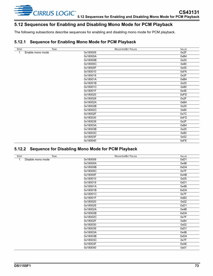
DS1155F1 73
CS431315.12 Sequences for Enabling and Disabling Mono Mode for PCM Playback
5.12 Sequences for Enabling and Disabling Mono Mode for PCM Playback
The following subsections describe sequences for enabling and disabling mono mode for PCM playback.
5.12.1 Sequence for Enabling Mono Mode for PCM Playback
5.12.2 Sequence for Disabling Mono Mode for PCM Playback
STEP TASK REGISTER/BIT FIELDS VALUE
1 Enable mono mode 0x180009 0x2F0x18000A 0xB40x18000B 0x250x18000C 0x800x18000F 0x550x180010 0xFA0x180019 0x2F0x18001A 0xB40x18001B 0x250x18001C 0x800x18001F 0x4E0x180020 0xFD0x180029 0x2F0x18002A 0xB40x18002B 0x250x18002C 0x800x18002F 0x7C0x180030 0xFD0x180039 0x2F0x18003A 0xB40x18003B 0x250x18003C 0x800x18003F 0x520x180040 0xFE
STEP TASK REGISTER/BIT FIELDS VALUE
1 Disable mono mode 0x180009 0xD10x18000A 0x4B0x18000B 0xDA0x18000C 0x7F0x18000F 0xAB0x180010 0x050x180019 0xD10x18001A 0x4B0x18001B 0xDA0x18001C 0x7F0x18001F 0xB20x180020 0x020x180029 0xD10x18002A 0x4B0x18002B 0xDA0x18002C 0x7F0x18002F 0x840x180030 0x020x180039 0xD10x18003A 0x4B0x18003B 0xDA0x18003C 0x7F0x18003F 0xAE0x180040 0x01

74 DS1155F1
CS431315.13 Example Sequences
5.13 Example Sequences
This section provides recommended instruction sequences for standard CS43131 operations.
5.13.1 Power-up Sequence to I2S Playback
In Ex. 5-7, a 22.5792-MHz crystal is used, ASP is set to I2S master at 44.1 kHz, and full-scale output is 1.732 Vrms.
Example 5-7. Startup to I2S Playback
STEP TASK REGISTER/BIT FIELDS VALUE DESCRIPTION
1 Apply all relevant power supplies, then assert RESET.2 Wait for 1.5 ms.3 Configure XTAL driver4 Configure XTAL bias
current strength (assuming River Crystal at 22.5792 MHz)
Crystal Setting. 0x20052 0x04ReservedXTAL_IBIAS
0000 0100 Bias current set to 12.5 µA
5 Read Interrupt Status 1 register (0xF0000) to clear any pending interrupts.6 Enable XTAL interrupts Interrupt Mask 1. 0xF0010 0xE7
DAC_OVFL_INT_MASKHPDETECT_PLUG_INT_MASKHPDETECT_UNPLUG_INT_MASKXTAL_READY_INT_MASKXTAL_ERROR_INT_MASKPLL_READY_INT_MASKPLL_ERROR_INT_MASKPDN_DONE_INT_MASK
11100111
Enable XTAL_READY interruptEnable XTAL_ERROR interrupt
7 Start XTAL Power Down Control. 0x20000 0xF6PDN_XSPPDN_ASPPDN_DSDIFPDN_HPPDN_XTALPDN_PLLPDN_CLKOUTReserved
11110110
Power up XTAL driver
8 Configure ASP interface. Sample rate set to 44.1 kHz. ASP is clock master.9 Set ASP sample rate Serial Port Sample Rate. 0x1000B 0x01
ReservedASP_SPRATE
00000001 Set sample rate to 44.1 kHz
10 Set ASP sample bit size. XSP is don't care
Serial Port Sample Bit Size. 0x1000C 0x04ReservedXSP_SPSIZEASP_SPSIZE
00000100
XSP sample bit size set to 24 bitsASP sample bit size set to 32 bits
11 Set ASP numerator ASP Numerator 1. 0x40010 0x01ASP_N_LSB 0x01 LSB of ASP sample rate fractional divide numerator
ASP Numerator 2. 0x40011 0x00ASP_N_MSB 0x00 MSB of ASP sample rate fractional divide numerator
12 Set ASP denominator ASP Denominator 1. 0x40012 0x08ASP_M_LSB 0x08 LSB of ASP sample rate fractional divide denominator
ASP Denominator 2. 0x40013 0x00ASP_M_MSB 0x00 MSB of ASP sample rate fractional divide denominator
13 Set ASP LRCK high time ASP LRCK High Time 1. 0x40014 0x1FASP_LCHI_LSB 0x1F LSB of ASP LRCK high time duration
ASP LRCK High Time 2. 0x40015 0x00ASP_LCHI_MSB 0x00 MSB of ASP LRCK high time duration
14 Set ASP LRCK period ASP LRCK Period 1. 0x40016 0x3FASP_LCPR_LSB 0x3F LSB of ASP LRCK period
ASP LRCK Period 2. 0x40017 0x00ASP_LCPR_MSB 0x00 MSB of ASP LRCK period
15 Configure ASP clock ASP Clock Configuration. 0x40018 0x1CReservedASP_M/SBASP_SCPOL_OUTASP_SCPOL_INASP_LCPOL_OUTASP_LCPOL_IN
00011100
Set ASP port to be masterConfigure clock polarity for I2S input
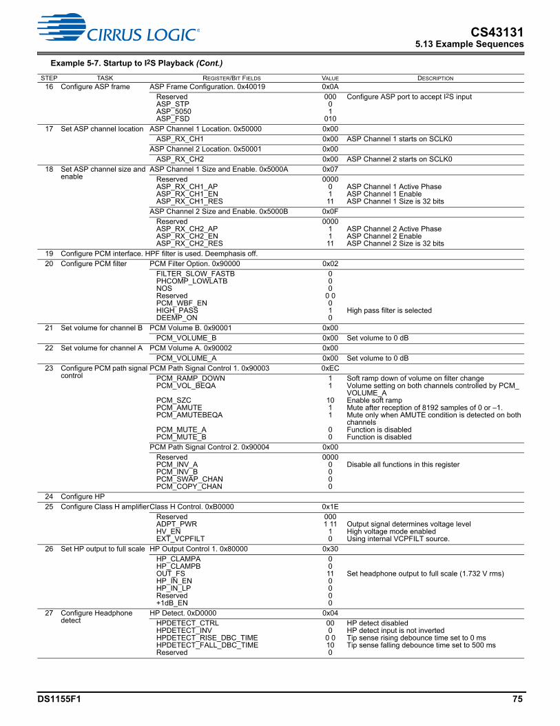
DS1155F1 75
CS431315.13 Example Sequences
16 Configure ASP frame ASP Frame Configuration. 0x40019 0x0AReservedASP_STPASP_5050ASP_FSD
00001
010
Configure ASP port to accept I2S input
17 Set ASP channel location ASP Channel 1 Location. 0x50000 0x00ASP_RX_CH1 0x00 ASP Channel 1 starts on SCLK0
ASP Channel 2 Location. 0x50001 0x00ASP_RX_CH2 0x00 ASP Channel 2 starts on SCLK0
18 Set ASP channel size and enable
ASP Channel 1 Size and Enable. 0x5000A 0x07ReservedASP_RX_CH1_APASP_RX_CH1_ENASP_RX_CH1_RES
00000111
ASP Channel 1 Active PhaseASP Channel 1 EnableASP Channel 1 Size is 32 bits
ASP Channel 2 Size and Enable. 0x5000B 0x0FReservedASP_RX_CH2_APASP_RX_CH2_ENASP_RX_CH2_RES
00001111
ASP Channel 2 Active PhaseASP Channel 2 EnableASP Channel 2 Size is 32 bits
19 Configure PCM interface. HPF filter is used. Deemphasis off.20 Configure PCM filter PCM Filter Option. 0x90000 0x02
FILTER_SLOW_FASTBPHCOMP_LOWLATBNOSReservedPCM_WBF_ENHIGH_PASSDEEMP_ON
000
0 0010
High pass filter is selected
21 Set volume for channel B PCM Volume B. 0x90001 0x00PCM_VOLUME_B 0x00 Set volume to 0 dB
22 Set volume for channel A PCM Volume A. 0x90002 0x00PCM_VOLUME_A 0x00 Set volume to 0 dB
23 Configure PCM path signal control
PCM Path Signal Control 1. 0x90003 0xECPCM_RAMP_DOWNPCM_VOL_BEQA
PCM_SZCPCM_AMUTEPCM_AMUTEBEQA
PCM_MUTE_APCM_MUTE_B
11
1011
00
Soft ramp down of volume on filter changeVolume setting on both channels controlled by PCM_VOLUME_AEnable soft rampMute after reception of 8192 samples of 0 or –1.Mute only when AMUTE condition is detected on both channelsFunction is disabledFunction is disabled
PCM Path Signal Control 2. 0x90004 0x00ReservedPCM_INV_APCM_INV_BPCM_SWAP_CHANPCM_COPY_CHAN
00000000
Disable all functions in this register
24 Configure HP 25 Configure Class H amplifierClass H Control. 0xB0000 0x1E
ReservedADPT_PWRHV_ENEXT_VCPFILT
0001 11
10
Output signal determines voltage levelHigh voltage mode enabledUsing internal VCPFILT source.
26 Set HP output to full scale HP Output Control 1. 0x80000 0x30HP_CLAMPA HP_CLAMPB OUT_FSHP_IN_EN HP_IN_LP Reserved+1dB_EN
00110000
Set headphone output to full scale (1.732 V rms)
27 Configure Headphone detect
HP Detect. 0xD0000 0x04HPDETECT_CTRLHPDETECT_INVHPDETECT_RISE_DBC_TIMEHPDETECT_FALL_DBC_TIMEReserved
000
0 0100
HP detect disabledHP detect input is not invertedTip sense rising debounce time set to 0 msTip sense falling debounce time set to 500 ms
Example 5-7. Startup to I2S Playback (Cont.)
STEP TASK REGISTER/BIT FIELDS VALUE DESCRIPTION
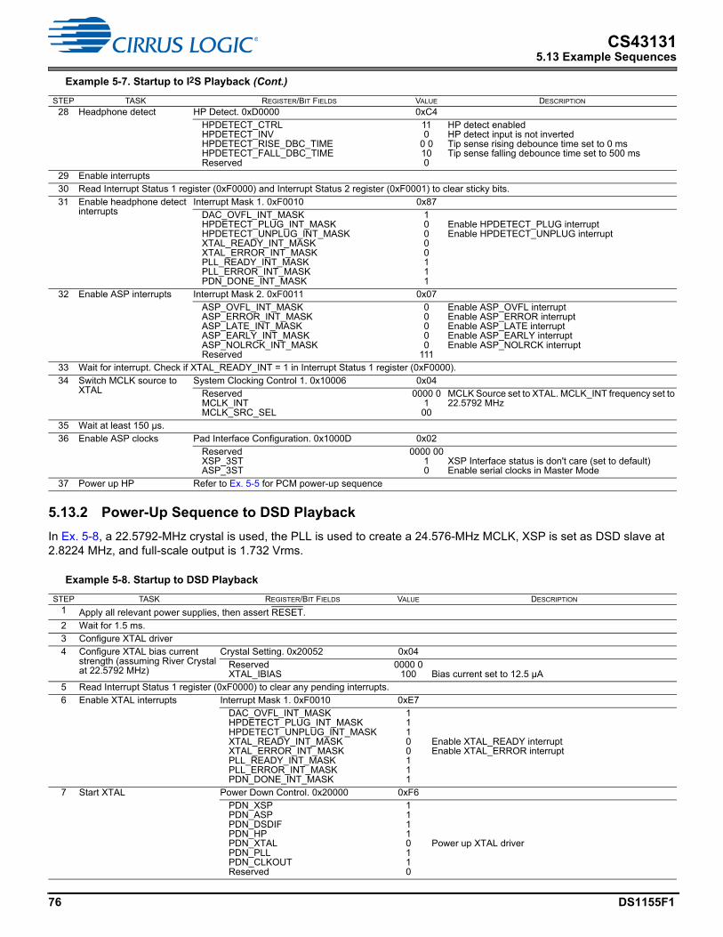
76 DS1155F1
CS431315.13 Example Sequences
5.13.2 Power-Up Sequence to DSD Playback
In Ex. 5-8, a 22.5792-MHz crystal is used, the PLL is used to create a 24.576-MHz MCLK, XSP is set as DSD slave at 2.8224 MHz, and full-scale output is 1.732 Vrms.
28 Headphone detect HP Detect. 0xD0000 0xC4HPDETECT_CTRLHPDETECT_INVHPDETECT_RISE_DBC_TIMEHPDETECT_FALL_DBC_TIMEReserved
110
0 0100
HP detect enabledHP detect input is not invertedTip sense rising debounce time set to 0 msTip sense falling debounce time set to 500 ms
29 Enable interrupts30 Read Interrupt Status 1 register (0xF0000) and Interrupt Status 2 register (0xF0001) to clear sticky bits.31 Enable headphone detect
interruptsInterrupt Mask 1. 0xF0010 0x87
DAC_OVFL_INT_MASKHPDETECT_PLUG_INT_MASKHPDETECT_UNPLUG_INT_MASKXTAL_READY_INT_MASKXTAL_ERROR_INT_MASKPLL_READY_INT_MASKPLL_ERROR_INT_MASKPDN_DONE_INT_MASK
10000111
Enable HPDETECT_PLUG interruptEnable HPDETECT_UNPLUG interrupt
32 Enable ASP interrupts Interrupt Mask 2. 0xF0011 0x07ASP_OVFL_INT_MASKASP_ERROR_INT_MASKASP_LATE_INT_MASKASP_EARLY_INT_MASKASP_NOLRCK_INT_MASKReserved
00000
111
Enable ASP_OVFL interruptEnable ASP_ERROR interruptEnable ASP_LATE interruptEnable ASP_EARLY interruptEnable ASP_NOLRCK interrupt
33 Wait for interrupt. Check if XTAL_READY_INT = 1 in Interrupt Status 1 register (0xF0000).34 Switch MCLK source to
XTALSystem Clocking Control 1. 0x10006 0x04
ReservedMCLK_INTMCLK_SRC_SEL
0000 0100
MCLK Source set to XTAL. MCLK_INT frequency set to 22.5792 MHz
35 Wait at least 150 µs.36 Enable ASP clocks Pad Interface Configuration. 0x1000D 0x02
ReservedXSP_3STASP_3ST
0000 0010
XSP Interface status is don't care (set to default)Enable serial clocks in Master Mode
37 Power up HP Refer to Ex. 5-5 for PCM power-up sequence
Example 5-8. Startup to DSD Playback
STEP TASK REGISTER/BIT FIELDS VALUE DESCRIPTION
1 Apply all relevant power supplies, then assert RESET.2 Wait for 1.5 ms.3 Configure XTAL driver4 Configure XTAL bias current
strength (assuming River Crystal at 22.5792 MHz)
Crystal Setting. 0x20052 0x04ReservedXTAL_IBIAS
0000 0100 Bias current set to 12.5 µA
5 Read Interrupt Status 1 register (0xF0000) to clear any pending interrupts.6 Enable XTAL interrupts Interrupt Mask 1. 0xF0010 0xE7
DAC_OVFL_INT_MASKHPDETECT_PLUG_INT_MASKHPDETECT_UNPLUG_INT_MASKXTAL_READY_INT_MASKXTAL_ERROR_INT_MASKPLL_READY_INT_MASKPLL_ERROR_INT_MASKPDN_DONE_INT_MASK
11100111
Enable XTAL_READY interruptEnable XTAL_ERROR interrupt
7 Start XTAL Power Down Control. 0x20000 0xF6PDN_XSPPDN_ASPPDN_DSDIFPDN_HPPDN_XTALPDN_PLLPDN_CLKOUTReserved
11110110
Power up XTAL driver
Example 5-7. Startup to I2S Playback (Cont.)
STEP TASK REGISTER/BIT FIELDS VALUE DESCRIPTION

DS1155F1 77
CS431315.13 Example Sequences
8 Configure PLL. Input is 22.5792 MHz. Output is 24.576 MHz.9 Power up PLL Power Down Control. 0x20000 0xF2
PDN_XSPPDN_ASPPDN_DSDIFPDN_HPPDN_XTALPDN_PLLPDN_CLKOUTReserved
11110010
Power up PLL
10 Set PLL predivide PLL Setting 9. 0x40002 0x03ReservedPLL_REF_PREDIV
0000 0011 Divide PLL Reference by 8
11 Set PLL Output Divide PLL Setting 6. 0x30008 0x08PLL_OUT_DIV 0x08 Divide PLL output by 8
12 Set Fractional portion of PLL divide ratio
PLL Setting 2. 0x30002 0x00PLL_DIV_FRAC_0 0x00
PLL Setting 3. 0x30003 0xF7PLL_DIV_FRAC_1 0xF7
PLL Setting 4. 0x30004 0x06PLL_DIV_FRAC_2 0x06
13 Set integer portion of PLL divide ratio
PLL Setting 5. 0x30005 0x44PLL_DIV_INT 0x44
14 Set PLL Mode PLL Setting 8. 0x3001B 0x01ReservedPLL_MODEReserved
0000 0001
Use 500/512 factor
15 Set PLL Calibration Ratio PLL Setting 7. 0x3000A 0x8BPLL_CAL_RATIO 0x8B Set PLL Cal Ratio to 139
16 Read Interrupt Status 1 register (0xF0000) to clear any pending interrupts.17 Enable PLL Interrupts Interrupt Mask 1. 0xF0010 0xE1
DAC_OVFL_INT_MASKHPDETECT_PLUG_INT_MASKHPDETECT_UNPLUG_INT_MASKXTAL_READY_INT_MASKXTAL_ERROR_INT_MASKPLL_READY_INT_MASKPLL_ERROR_INT_MASKPDN_DONE_INT_MASK
11100001
Enable PLL Ready and Error Interrupts
18 Start PLL PLL Setting 1. 0x30001 0x01ReservedPLL_START
0000 0001 Start PLL
19 Configure DSDIF to playback 64•Fs DSD stream. DSDIF is configured as Slave20 Configure DSD Volume DSD Volume A. 0x70001 0x00
DSD_VOLUME_A 0x00 Channel A volume set to 0dB21 Configure DSD path Signal
Control1DSD Processor Path Signal Control 1. 0x70002
0xCC
DSD_RAMP_UPDSD_VOL_BEQADSD_SZCReservedDSD_AMUTE
DSD_AMUTE_BEQA
DSD_MUTE_ADSD_MUTE_B
11001
1
00
DSD Volume B equals DSD volume AImmediate change
Mute occurs after 256 repeated 8-bit DSD mute patterns
Mute happens only when mute pattern is detected in both channelsFunction is disabledFunction is disabled
22 Configure DSD Interface DSD Interface Configuration. 0x70003 0x00ReservedDSD_M/SBDSD_PM_ENDSD_PM_SEL
0000 0000
DSD is clock slaveFunction is disabledFunction is disabled
Example 5-8. Startup to DSD Playback (Cont.)
STEP TASK REGISTER/BIT FIELDS VALUE DESCRIPTION
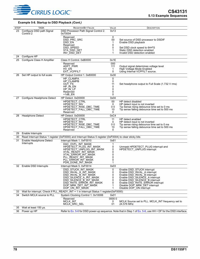
78 DS1155F1
CS431315.13 Example Sequences
23 Configure DSD path Signal Control 2
DSD Processor Path Signal Control 2. 0x70004
0x13
ReservedDSD_PRC_SRCDSD_ENReservedDSD_SPEEDSTA_DSD_DETINV_DSD_DET
00010011
Set source of DSD processor to DSDIFEnable DSD playback
Set DSD clock speed to 64•FSStatic DSD detection enabledInvalid DSD detection enabled
24 Configure HP 25 Configure Class H Amplifier Class H Control. 0xB0000 0x1E
ReservedADPT_PWRHV_ENEXT_VCPFILT
00011110
Output signal determines voltage levelHigh Voltage Mode Enabled Using Internal VCPFILT source.
26 Set HP output to full scale HP Output Control 1. 0x80000 0x30HP_CLAMPA HP_CLAMPB OUT_FSHP_IN_EN HP_IN_LP Reserved+1dB_EN
00110000
Set headphone output to Full Scale (1.732 V rms)
27 Configure Headphone Detect HP Detect. 0xD0000 0x04HPDETECT_CTRLHPDETECT_INVHPDETECT_RISE_DBC_TIMEHPDETECT_FALL_DBC_TIMEReserved
000
0 0100
HP detect disabledHP detect input is not invertedTip Sense rising debounce time set to 0 msTip sense falling debounce time set to 500 ms
28 Headphone Detect HP Detect. 0xD0000 0xC4HPDETECT_CTRLHPDETECT_INVHPDETECT_RISE_DBC_TIMEHPDETECT_FALL_DBC_TIMEReserved
110
0 0100
HP detect enabledHP detect input is not invertedTip sense rising debounce time set to 0 msTip sense falling debounce time set to 500 ms
29 Enable Interrupts30 Read Interrupt Status 1 register (0xF0000) and Interrupt Status 5 register (0xF0004) to clear sticky bits31 Enable Headphone Detect
InterruptsInterrupt Mask 1. 0xF0010 0x81
DAC_OVFL_INT_MASKHPDETECT_PLUG_INT_MASKHPDETECT_UNPLUG_INT_MASKXTAL_READY_INT_MASKXTAL_ERROR_INT_MASKPLL_READY_INT_MASKPLL_ERROR_INT_MASKPDN_DONE_INT_MASK
10000001
Unmask HPDETECT_PLUG interrupt andHPDETECT_UNPLUG interrupt
32 Enable DSD Interrupts Interrupt Mask 5. 0xF0014 0x03DSD_STUCK_INT_MASKDSD_INVAL_A_INT_MASKDSD_INVAL_B_INT_MASKDSD_SILENCE_A_INT_MASKDSD_SILENCE_B_INT_MASKDSD_RATE_ERROR_INT_MASKDOP_MRK_DET_INT_MASKDOP_ON_INT_MASK
00000011
Enable DSD_STUCK interruptEnable DSD_INVAL_A interruptEnable DSD_INVAL_B interruptEnable DSD_SILENCE_A interruptEnable DSD_SILENCE_B interruptEnable DSD_RATE_ERROR interruptDisable DOP_MRK_DET interruptDisable DOP_ON interrupt
33 Wait for interrupt. Check if PLL_READY_INT = 1 in Interrupt Status 1 register(0xF0000)34 Switch MCLK source to PLL System Clocking Control 1. 0x10006 0x01
ReservedMCLK_INTMCLK_SRC_SEL
0000 0001
MCLK Source set to PLL. MCLK_INT frequency set to 24.576 MHz
35 Wait at least 150 µs.36 Power up HP Refer to Ex. 5-6 for DSD power-up sequence. Note that in Step 1 of Ex. 5-6, use HH = DF for the DSD interface.
Example 5-8. Startup to DSD Playback (Cont.)
STEP TASK REGISTER/BIT FIELDS VALUE DESCRIPTION

DS1155F1 79
CS431315.13 Example Sequences
5.13.3 Power-Up Sequence to DoP Playback with PLL
In Ex. 5-9, an external 19.2-MHz MCLK is used with a PLL to generate an internal MCLK or 22.5792 MHz, and the ASP is in clock master receiving DoP data with LRCLK at 176.4 kHz and SCLK at 8.4672 MHz.
Example 5-9. DoP Playback with PLL
STEP TASK REGISTER/BIT FIELDS VALUE DESCRIPTION
1 Apply all relevant power supplies, then assert RESET.2 Wait for 1.5 ms.3 Configure PLL. XTI/MCLK input coming from an external 19.2 MHz source with PLL output set to 22.5792 MHz. Refer to Section 4.7.2 for register
settings for other frequency combinations4 Power up PLL Power Down Control. 0x20000 0xFA
PDN_XSPPDN_ASPPDN_DSDIFPDN_HPPDN_XTALPDN_PLLPDN_CLKOUTReserved
xxxxx0x0
Power up PLL block
5 Set PLL Predivide value PLL Setting 9. 0x40002 0x03ReservedPLL_REF_PREDIV
0000 0011 Set PLL predivide value to 8
6 Set PLL output divide PLL Setting 6. 0x30008 0x08PLL_OUT_DIV 0x08 Set PLL output divide value to 8
7 Set Fractional portion of PLL Divide Ratio PLL Setting 2. 0x30002 0x00PLL_DIV_FRAC_0 0x00 Set LSB of PLL fractional divider value to 0
PLL Setting 3. 0x30003 0x00PLL_DIV_FRAC_1 0x00 Set Middle Byte of PLL fractional divider value to 0
PLL Setting 4. 0x30004 0x80PLL_DIV_FRAC_2 0x80 Set MSB of PLL fractional divider value to 0x80
8 Set Integer portion of PLL Divide Ratio PLL Setting 5. 0x30005 0x49PLL_DIV_INT 0x49 Set PLL integer Divide value to 0x49
9 Set PLL mode PLL Setting 8. 0x3001B 0x01ReservedPLL_MODEReserved
0000 0001
500/512 factor is used in PLL frequency calculation
10 Read Interrupt Status 1 register (0xF0000) to clear sticky bits.11 Set PLL calibration ratio PLL Setting 7. 0x3000A 0x97
PLL_CAL_RATIO 0x97 PLL Calibration Ratio is set to 0x97 (151)12 Enable PLL interrupts Interrupt Mask 1. 0xF0010 0xF9
DAC_OVFL_INT_MASKHPDETECT_PLUG_INT_MASKHPDETECT_UNPLUG_INT_MASKXTAL_READY_INT_MASKXTAL_ERROR_INT_MASKPLL_READY_INT_MASKPLL_ERROR_INT_MASKPDN_DONE_INT_MASK
11111001
DAC_OVFL_INT is don't careUnmask HPDETECT_PLUG interruptUnmask HPDETECT_UNPLUG interruptXTAL_READY_INT is Don't CareXTAL_ERROR_INT is Don't CarePLL_READY Interrupt is already unmaskedPLL_ERROR Interrupt is already unmaskedPDN_DONE_INT is Don't Care
13 Start PLL PLL Setting 1. 0x30001 0x01ReservedPLL_START
0000 0001 Enable PLL Output
14 Playback DoP audio. Assuming 64•Fs DSD stream15 Configure ASP interface for DoP input16 Set ASP sample rate Serial Port Sample Rate. 0x1000B 0x05
ReservedASP_SPRATE
00000101 Set sample rate to 176.4 kHz
17 Set ASP sample bit size. XSP is don't care Serial Port Sample Bit Size. 0x1000C 0x05ReservedXSP_SPSIZEASP_SPSIZE
00000101
XSP sample bit size set to 24 bitsASP sample bit size set to 24 bits
18 Set ASP numerator ASP Numerator 1. 0x40010 0x03ASP_N_LSB 0x03 LSB of ASP sample rate fractional divide
numeratorASP Numerator 2. 0x40011 0x00
ASP_N_MSB 0x00 MSB of ASP sample rate fractional divide numerator
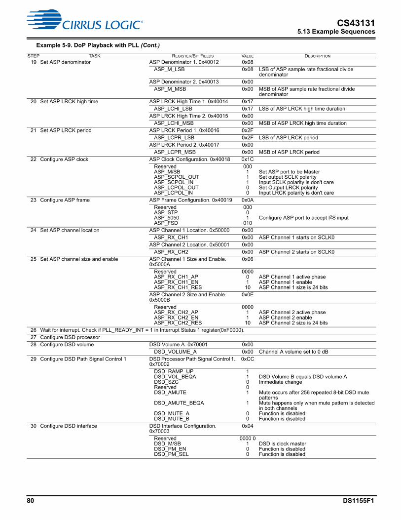
80 DS1155F1
CS431315.13 Example Sequences
19 Set ASP denominator ASP Denominator 1. 0x40012 0x08ASP_M_LSB 0x08 LSB of ASP sample rate fractional divide
denominatorASP Denominator 2. 0x40013 0x00
ASP_M_MSB 0x00 MSB of ASP sample rate fractional divide denominator
20 Set ASP LRCK high time ASP LRCK High Time 1. 0x40014 0x17ASP_LCHI_LSB 0x17 LSB of ASP LRCK high time duration
ASP LRCK High Time 2. 0x40015 0x00ASP_LCHI_MSB 0x00 MSB of ASP LRCK high time duration
21 Set ASP LRCK period ASP LRCK Period 1. 0x40016 0x2FASP_LCPR_LSB 0x2F LSB of ASP LRCK period
ASP LRCK Period 2. 0x40017 0x00ASP_LCPR_MSB 0x00 MSB of ASP LRCK period
22 Configure ASP clock ASP Clock Configuration. 0x40018 0x1CReservedASP_M/SBASP_SCPOL_OUTASP_SCPOL_INASP_LCPOL_OUTASP_LCPOL_IN
00011100
Set ASP port to be MasterSet output SCLK polarityInput SCLK polarity is don't careSet Output LRCK polarityInput LRCK polarity is don't care
23 Configure ASP frame ASP Frame Configuration. 0x40019 0x0AReservedASP_STPASP_5050ASP_FSD
00001
010Configure ASP port to accept I2S input
24 Set ASP channel location ASP Channel 1 Location. 0x50000 0x00ASP_RX_CH1 0x00 ASP Channel 1 starts on SCLK0
ASP Channel 2 Location. 0x50001 0x00ASP_RX_CH2 0x00 ASP Channel 2 starts on SCLK0
25 Set ASP channel size and enable ASP Channel 1 Size and Enable. 0x5000A
0x06
ReservedASP_RX_CH1_APASP_RX_CH1_ENASP_RX_CH1_RES
00000110
ASP Channel 1 active phaseASP Channel 1 enableASP Channel 1 size is 24 bits
ASP Channel 2 Size and Enable. 0x5000B
0x0E
ReservedASP_RX_CH2_APASP_RX_CH2_ENASP_RX_CH2_RES
00001110
ASP Channel 2 active phaseASP Channel 2 enableASP Channel 2 size is 24 bits
26 Wait for interrupt. Check if PLL_READY_INT = 1 in Interrupt Status 1 register(0xF0000).27 Configure DSD processor28 Configure DSD volume DSD Volume A. 0x70001 0x00
DSD_VOLUME_A 0x00 Channel A volume set to 0 dB29 Configure DSD Path Signal Control 1 DSD Processor Path Signal Control 1.
0x700020xCC
DSD_RAMP_UPDSD_VOL_BEQADSD_SZCReservedDSD_AMUTE
DSD_AMUTE_BEQA
DSD_MUTE_ADSD_MUTE_B
11001
1
00
DSD Volume B equals DSD volume AImmediate change
Mute occurs after 256 repeated 8-bit DSD mute patternsMute happens only when mute pattern is detected in both channelsFunction is disabledFunction is disabled
30 Configure DSD interface DSD Interface Configuration. 0x70003
0x04
ReservedDSD_M/SBDSD_PM_ENDSD_PM_SEL
0000 0100
DSD is clock masterFunction is disabledFunction is disabled
Example 5-9. DoP Playback with PLL (Cont.)
STEP TASK REGISTER/BIT FIELDS VALUE DESCRIPTION

DS1155F1 81
CS431315.13 Example Sequences
31 Configure DSD Path Signal Control 2 DSD Processor Path Signal Control 2. 0x70004
0x50
ReservedDSD_PRC_SRCDSD_ENReservedDSD_SPEEDSTA_DSD_DETINV_DSD_DET
01010000
Set source of DSD processor to ASPEnable DSD playback
Set DSD clock speed to 64•FsStatic DSD detection disabledInvalid DSD detection disabled
32 Configure DSD path Signal Control 3 DSD Processor Path Signal Control 3. 0x70006
0xC0
DSD_ZERODB
DSD_HPF_ENReservedSIGCTL_DSDEQPCMDSD_INV_ADSD_INV_BDSD_SWAP_CHANDSD_COPY_CHAN
1
1000000
The SACD 0–dB reference level (50%modulation index) matches PCM 0-dB full scale.Enable HPF in DSD processor
Function is disabledFunction is disabledFunction is disabledFunction is disabledFunction is disabled
33 Configure headphone output for 1.732 V rms34 Configure Class H amplifier Class H Control. 0xB0000 0x1E
ReservedADPT_PWRHV_ENEXT_VCPFILT
0001 11
10
Output signal determines voltage levelHigh voltage mode enabled Using internal VCPFILT source.
35 Set HP output to full scale HP Output Control 1. 0x80000 0x30HP_CLAMPA HP_CLAMPB OUT_FSHP_IN_EN HP_IN_LP Reserved+1dB_EN
00110000
Set headphone output to full scale (1.732 V rms)
36 Headphone detect HP Detect. 0xD0000 0xC4HPDETECT_CTRLHPDETECT_INVHPDETECT_RISE_DBC_TIMEHPDETECT_FALL_DBC_TIMEReserved
110
0 0100
HP detect enabledHP detect input is not invertedTip Sense rising debounce time set to 0 msTip sense falling debounce time set to 500 ms
37 Enable interrupts38 Read Interrupt Status 1 register (0xF0000), Interrupt Status 2 register (0xF0001) and Interrupt Status 5 register (0xF0004) to clear sticky bits.39 Enable headphone detect interrupts Interrupt Mask 1. 0xF0010 0x99
DAC_OVFL_INT_MASKHPDETECT_PLUG_INT_MASKHPDETECT_UNPLUG_INT_MASKXTAL_READY_INT_MASKXTAL_ERROR_INT_MASKPLL_READY_INT_MASKPLL_ERROR_INT_MASKPDN_DONE_INT_MASK
10011001
DAC_OVFL_INT is don't careEnable HPDETECT_PLUG interruptEnable HPDETECT_UNPLUG interruptXTAL_READY_INT is don't careXTAL_ERROR_INT is don't carePLL_READY interrupt already enabledPLL_ERROR interrupt already enabledPDN_DONE_INT is don't care
40 Enable ASP interrupts Interrupt Mask 2. 0xF0011 0x07ASP_OVFL_INT_MASKASP_ERROR_INT_MASKASP_LATE_INT_MASKASP_EARLY_INT_MASKASP_NOLRCK_INT_MASKReserved
00000
111
Enable ASP_OVFL interruptEnable ASP_ERROR interruptEnable ASP_LATE interruptEnable ASP_EARLY interruptEnable ASP_NOLRCK interrupt
41 Enable DSD and DoP interrupts Interrupt Mask 5. 0xF0014 0x01DSD_STUCK_INT_MASKDSD_INVAL_A_INT_MASKDSD_INVAL_B_INT_MASKDSD_SILENCE_A_INT_MASKDSD_SILENCE_B_INT_MASKDSD_RATE_ERROR_INT_MASKDOP_MRK_DET_INT_MASKDOP_ON_INT_MASK
00000001
Enable DSD_STUCK interruptEnable DSD_INVAL_A interruptEnable DSD_INVAL_B interruptEnable DSD_SILENCE_A interruptEnable DSD_SILENCE_B interruptEnable DSD_RATE_ERROR interruptEnable DOP_MRK_DET interruptDisable DOP_ON interrupt
42 Wait for interrupt. Check if PLL_READY_INT = 1 in Interrupt Status 1 register(0xF0000).43 Set MCLK source and frequency System Clocking Control. 0x10006 0x05
ReservedMCLK_INTMCLK_SRC_SEL
0000 0101
MCLK Frequency is set to 22.5792 MHzMCLK Source is set to PLL
44 Wait for at least 150 µs.
Example 5-9. DoP Playback with PLL (Cont.)
STEP TASK REGISTER/BIT FIELDS VALUE DESCRIPTION
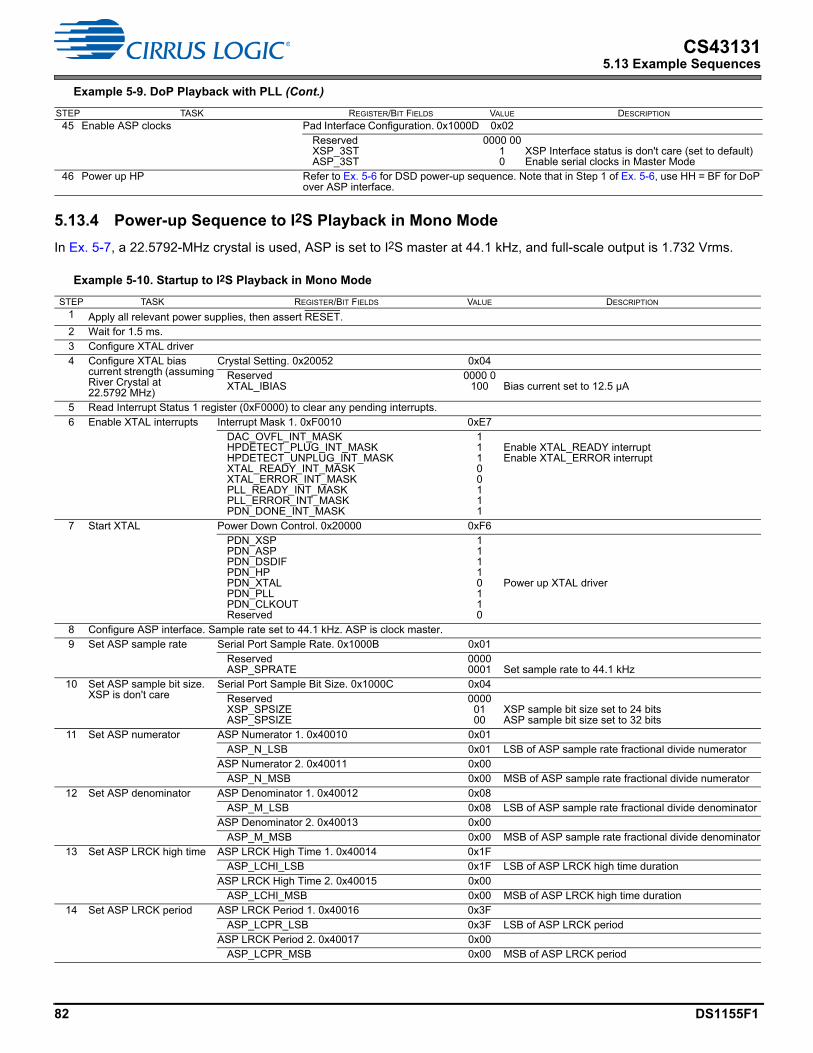
82 DS1155F1
CS431315.13 Example Sequences
5.13.4 Power-up Sequence to I2S Playback in Mono Mode
In Ex. 5-7, a 22.5792-MHz crystal is used, ASP is set to I2S master at 44.1 kHz, and full-scale output is 1.732 Vrms.
45 Enable ASP clocks Pad Interface Configuration. 0x1000D 0x02ReservedXSP_3STASP_3ST
0000 0010
XSP Interface status is don't care (set to default)Enable serial clocks in Master Mode
46 Power up HP Refer to Ex. 5-6 for DSD power-up sequence. Note that in Step 1 of Ex. 5-6, use HH = BF for DoP over ASP interface.
Example 5-10. Startup to I2S Playback in Mono Mode
STEP TASK REGISTER/BIT FIELDS VALUE DESCRIPTION
1 Apply all relevant power supplies, then assert RESET.2 Wait for 1.5 ms.3 Configure XTAL driver4 Configure XTAL bias
current strength (assuming River Crystal at 22.5792 MHz)
Crystal Setting. 0x20052 0x04ReservedXTAL_IBIAS
0000 0100 Bias current set to 12.5 µA
5 Read Interrupt Status 1 register (0xF0000) to clear any pending interrupts.6 Enable XTAL interrupts Interrupt Mask 1. 0xF0010 0xE7
DAC_OVFL_INT_MASKHPDETECT_PLUG_INT_MASKHPDETECT_UNPLUG_INT_MASKXTAL_READY_INT_MASKXTAL_ERROR_INT_MASKPLL_READY_INT_MASKPLL_ERROR_INT_MASKPDN_DONE_INT_MASK
11100111
Enable XTAL_READY interruptEnable XTAL_ERROR interrupt
7 Start XTAL Power Down Control. 0x20000 0xF6PDN_XSPPDN_ASPPDN_DSDIFPDN_HPPDN_XTALPDN_PLLPDN_CLKOUTReserved
11110110
Power up XTAL driver
8 Configure ASP interface. Sample rate set to 44.1 kHz. ASP is clock master.9 Set ASP sample rate Serial Port Sample Rate. 0x1000B 0x01
ReservedASP_SPRATE
00000001 Set sample rate to 44.1 kHz
10 Set ASP sample bit size. XSP is don't care
Serial Port Sample Bit Size. 0x1000C 0x04ReservedXSP_SPSIZEASP_SPSIZE
00000100
XSP sample bit size set to 24 bitsASP sample bit size set to 32 bits
11 Set ASP numerator ASP Numerator 1. 0x40010 0x01ASP_N_LSB 0x01 LSB of ASP sample rate fractional divide numerator
ASP Numerator 2. 0x40011 0x00ASP_N_MSB 0x00 MSB of ASP sample rate fractional divide numerator
12 Set ASP denominator ASP Denominator 1. 0x40012 0x08ASP_M_LSB 0x08 LSB of ASP sample rate fractional divide denominator
ASP Denominator 2. 0x40013 0x00ASP_M_MSB 0x00 MSB of ASP sample rate fractional divide denominator
13 Set ASP LRCK high time ASP LRCK High Time 1. 0x40014 0x1FASP_LCHI_LSB 0x1F LSB of ASP LRCK high time duration
ASP LRCK High Time 2. 0x40015 0x00ASP_LCHI_MSB 0x00 MSB of ASP LRCK high time duration
14 Set ASP LRCK period ASP LRCK Period 1. 0x40016 0x3FASP_LCPR_LSB 0x3F LSB of ASP LRCK period
ASP LRCK Period 2. 0x40017 0x00ASP_LCPR_MSB 0x00 MSB of ASP LRCK period
Example 5-9. DoP Playback with PLL (Cont.)
STEP TASK REGISTER/BIT FIELDS VALUE DESCRIPTION
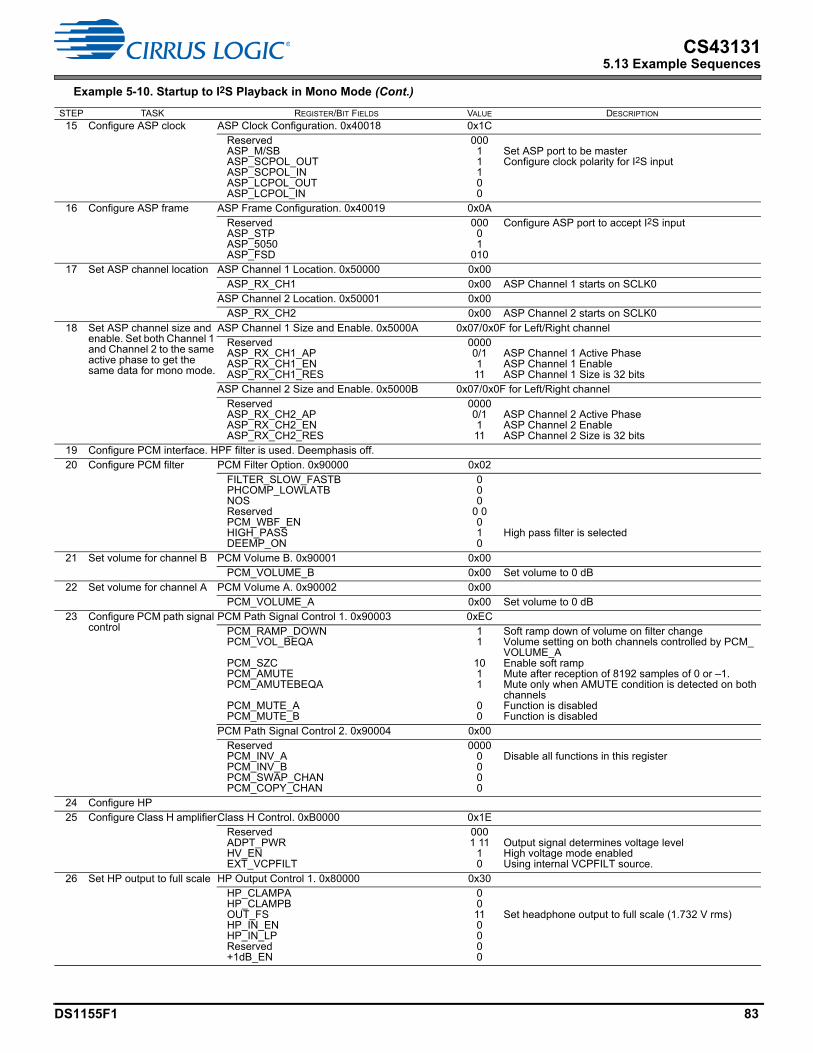
DS1155F1 83
CS431315.13 Example Sequences
15 Configure ASP clock ASP Clock Configuration. 0x40018 0x1CReservedASP_M/SBASP_SCPOL_OUTASP_SCPOL_INASP_LCPOL_OUTASP_LCPOL_IN
00011100
Set ASP port to be masterConfigure clock polarity for I2S input
16 Configure ASP frame ASP Frame Configuration. 0x40019 0x0AReservedASP_STPASP_5050ASP_FSD
00001
010
Configure ASP port to accept I2S input
17 Set ASP channel location ASP Channel 1 Location. 0x50000 0x00ASP_RX_CH1 0x00 ASP Channel 1 starts on SCLK0
ASP Channel 2 Location. 0x50001 0x00ASP_RX_CH2 0x00 ASP Channel 2 starts on SCLK0
18 Set ASP channel size and enable. Set both Channel 1 and Channel 2 to the same active phase to get the same data for mono mode.
ASP Channel 1 Size and Enable. 0x5000A 0x07/0x0F for Left/Right channelReservedASP_RX_CH1_APASP_RX_CH1_ENASP_RX_CH1_RES
00000/1111
ASP Channel 1 Active PhaseASP Channel 1 EnableASP Channel 1 Size is 32 bits
ASP Channel 2 Size and Enable. 0x5000B 0x07/0x0F for Left/Right channelReservedASP_RX_CH2_APASP_RX_CH2_ENASP_RX_CH2_RES
00000/1111
ASP Channel 2 Active PhaseASP Channel 2 EnableASP Channel 2 Size is 32 bits
19 Configure PCM interface. HPF filter is used. Deemphasis off.20 Configure PCM filter PCM Filter Option. 0x90000 0x02
FILTER_SLOW_FASTBPHCOMP_LOWLATBNOSReservedPCM_WBF_ENHIGH_PASSDEEMP_ON
000
0 0010
High pass filter is selected
21 Set volume for channel B PCM Volume B. 0x90001 0x00PCM_VOLUME_B 0x00 Set volume to 0 dB
22 Set volume for channel A PCM Volume A. 0x90002 0x00PCM_VOLUME_A 0x00 Set volume to 0 dB
23 Configure PCM path signal control
PCM Path Signal Control 1. 0x90003 0xECPCM_RAMP_DOWNPCM_VOL_BEQA
PCM_SZCPCM_AMUTEPCM_AMUTEBEQA
PCM_MUTE_APCM_MUTE_B
11
1011
00
Soft ramp down of volume on filter changeVolume setting on both channels controlled by PCM_VOLUME_AEnable soft rampMute after reception of 8192 samples of 0 or –1.Mute only when AMUTE condition is detected on both channelsFunction is disabledFunction is disabled
PCM Path Signal Control 2. 0x90004 0x00ReservedPCM_INV_APCM_INV_BPCM_SWAP_CHANPCM_COPY_CHAN
00000000
Disable all functions in this register
24 Configure HP 25 Configure Class H amplifierClass H Control. 0xB0000 0x1E
ReservedADPT_PWRHV_ENEXT_VCPFILT
0001 11
10
Output signal determines voltage levelHigh voltage mode enabledUsing internal VCPFILT source.
26 Set HP output to full scale HP Output Control 1. 0x80000 0x30HP_CLAMPA HP_CLAMPB OUT_FSHP_IN_EN HP_IN_LP Reserved+1dB_EN
00110000
Set headphone output to full scale (1.732 V rms)
Example 5-10. Startup to I2S Playback in Mono Mode (Cont.)
STEP TASK REGISTER/BIT FIELDS VALUE DESCRIPTION
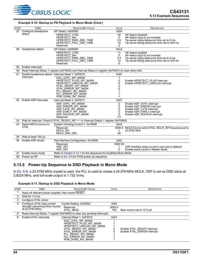
84 DS1155F1
CS431315.13 Example Sequences
5.13.5 Power-Up Sequence to DSD Playback in Mono Mode
In Ex. 5-8, a 22.5792-MHz crystal is used, the PLL is used to create a 24.576-MHz MCLK, XSP is set as DSD slave at 2.8224 MHz, and full-scale output is 1.732 Vrms.
27 Configure Headphone detect
HP Detect. 0xD0000 0x04HPDETECT_CTRLHPDETECT_INVHPDETECT_RISE_DBC_TIMEHPDETECT_FALL_DBC_TIMEReserved
000
0 0100
HP detect disabledHP detect input is not invertedTip sense rising debounce time set to 0 msTip sense falling debounce time set to 500 ms
28 Headphone detect HP Detect. 0xD0000 0xC4HPDETECT_CTRLHPDETECT_INVHPDETECT_RISE_DBC_TIMEHPDETECT_FALL_DBC_TIMEReserved
110
0 0100
HP detect enabledHP detect input is not invertedTip sense rising debounce time set to 0 msTip sense falling debounce time set to 500 ms
29 Enable interrupts30 Read Interrupt Status 1 register (0xF0000) and Interrupt Status 2 register (0xF0001) to clear sticky bits.31 Enable headphone detect
interruptsInterrupt Mask 1. 0xF0010 0x87
DAC_OVFL_INT_MASKHPDETECT_PLUG_INT_MASKHPDETECT_UNPLUG_INT_MASKXTAL_READY_INT_MASKXTAL_ERROR_INT_MASKPLL_READY_INT_MASKPLL_ERROR_INT_MASKPDN_DONE_INT_MASK
10000111
Enable HPDETECT_PLUG interruptEnable HPDETECT_UNPLUG interrupt
32 Enable ASP interrupts Interrupt Mask 2. 0xF0011 0x07ASP_OVFL_INT_MASKASP_ERROR_INT_MASKASP_LATE_INT_MASKASP_EARLY_INT_MASKASP_NOLRCK_INT_MASKReserved
00000
111
Enable ASP_OVFL interruptEnable ASP_ERROR interruptEnable ASP_LATE interruptEnable ASP_EARLY interruptEnable ASP_NOLRCK interrupt
33 Wait for interrupt. Check if XTAL_READY_INT = 1 in Interrupt Status 1 register (0xF0000).34 Switch MCLK source to
XTALSystem Clocking Control 1. 0x10006 0x04
ReservedMCLK_INTMCLK_SRC_SEL
0000 0100
MCLK Source set to XTAL. MCLK_INT frequency set to 22.5792 MHz
35 Wait at least 150 µs.36 Enable ASP clocks Pad Interface Configuration. 0x1000D 0x02
ReservedXSP_3STASP_3ST
0000 0010
XSP Interface status is don't care (set to default)Enable serial clocks in Master Mode
37 Enable mono mode Refer to Section 5.12.1 for the Sequence for Enabling Mono Mode38 Power up HP Refer to Ex. 5-5 for PCM power-up sequence
Example 5-11. Startup to DSD Playback in Mono Mode
STEP TASK REGISTER/BIT FIELDS VALUE DESCRIPTION
1 Apply all relevant power supplies, then assert RESET.2 Wait for 1.5 ms.3 Configure XTAL driver4 Configure XTAL bias current
strength (assuming River Crystal at 22.5792 MHz)
Crystal Setting. 0x20052 0x04ReservedXTAL_IBIAS
0000 0100 Bias current set to 12.5 µA
5 Read Interrupt Status 1 register (0xF0000) to clear any pending interrupts.6 Enable XTAL interrupts Interrupt Mask 1. 0xF0010 0xE7
DAC_OVFL_INT_MASKHPDETECT_PLUG_INT_MASKHPDETECT_UNPLUG_INT_MASKXTAL_READY_INT_MASKXTAL_ERROR_INT_MASKPLL_READY_INT_MASKPLL_ERROR_INT_MASKPDN_DONE_INT_MASK
11100111
Enable XTAL_READY interruptEnable XTAL_ERROR interrupt
Example 5-10. Startup to I2S Playback in Mono Mode (Cont.)
STEP TASK REGISTER/BIT FIELDS VALUE DESCRIPTION

DS1155F1 85
CS431315.13 Example Sequences
7 Start XTAL Power Down Control. 0x20000 0xF6PDN_XSPPDN_ASPPDN_DSDIFPDN_HPPDN_XTALPDN_PLLPDN_CLKOUTReserved
11110110
Power up XTAL driver
8 Configure PLL. Input is 22.5792 MHz. Output is 24.576 MHz.9 Power up PLL Power Down Control. 0x20000 0xF2
PDN_XSPPDN_ASPPDN_DSDIFPDN_HPPDN_XTALPDN_PLLPDN_CLKOUTReserved
11110010
Power up PLL
10 Set PLL predivide PLL Setting 9. 0x40002 0x03ReservedPLL_REF_PREDIV
0000 0011 Divide PLL Reference by 8
11 Set PLL Output Divide PLL Setting 6. 0x30008 0x08PLL_OUT_DIV 0x08 Divide PLL output by 8
12 Set Fractional portion of PLL divide ratio
PLL Setting 2. 0x30002 0x00PLL_DIV_FRAC_0 0x00
PLL Setting 3. 0x30003 0xF7PLL_DIV_FRAC_1 0xF7
PLL Setting 4. 0x30004 0x06PLL_DIV_FRAC_2 0x06
13 Set integer portion of PLL divide ratio
PLL Setting 5. 0x30005 0x44PLL_DIV_INT 0x44
14 Set PLL Mode PLL Setting 8. 0x3001B 0x01ReservedPLL_MODEReserved
0000 0001
Use 500/512 factor
15 Set PLL Calibration Ratio PLL Setting 7. 0x3000A 0x8BPLL_CAL_RATIO 0x8B Set PLL Cal Ratio to 139
16 Read Interrupt Status 1 register (0xF0000) to clear any pending interrupts.17 Enable PLL Interrupts Interrupt Mask 1. 0xF0010 0xE1
DAC_OVFL_INT_MASKHPDETECT_PLUG_INT_MASKHPDETECT_UNPLUG_INT_MASKXTAL_READY_INT_MASKXTAL_ERROR_INT_MASKPLL_READY_INT_MASKPLL_ERROR_INT_MASKPDN_DONE_INT_MASK
11100001
Enable PLL Ready and Error Interrupts
18 Start PLL PLL Setting 1. 0x30001 0x01ReservedPLL_START
0000 0001 Start PLL
19 Configure DSDIF to playback 64•Fs DSD stream. DSDIF is configured as Slave20 Configure DSD Volume DSD Volume A. 0x70001 0x00
DSD_VOLUME_A 0x00 Channel A volume set to 0dB21 Configure DSD path Signal
Control1DSD Processor Path Signal Control 1. 0x70002
0xCC
DSD_RAMP_UPDSD_VOL_BEQADSD_SZCReservedDSD_AMUTE
DSD_AMUTE_BEQA
DSD_MUTE_ADSD_MUTE_B
11001
1
00
DSD Volume B equals DSD volume AImmediate change
Mute occurs after 256 repeated 8-bit DSD mute patterns
Mute happens only when mute pattern is detected in both channelsFunction is disabledFunction is disabled
Example 5-11. Startup to DSD Playback in Mono Mode (Cont.)
STEP TASK REGISTER/BIT FIELDS VALUE DESCRIPTION

86 DS1155F1
CS431315.13 Example Sequences
22 Configure DSD Interface DSD Interface Configuration. 0x70003 0x00ReservedDSD_M/SBDSD_PM_ENDSD_PM_SEL
0000 0000
DSD is clock slaveFunction is disabledFunction is disabled
23 Configure DSD path Signal Control 2
DSD Processor Path Signal Control 2. 0x70004
0x13
ReservedDSD_PRC_SRCDSD_ENReservedDSD_SPEEDSTA_DSD_DETINV_DSD_DET
00010011
Set source of DSD processor to DSDIFEnable DSD playback
Set DSD clock speed to 64•FSStatic DSD detection enabledInvalid DSD detection enabled
24 Configure DSD path Signal Control 3. Enable mono mode:
a. Select Channel A/B(DSD_SWAP_CHAN)
b. Copy Channel A to B (DSD_COPY_CHAN)
c. Invert Channel B (DSD_INV_B)
DSD Processor Path Signal Control 3. 0x70006
0xC5/0xC7 for Left/Right channel
DSD_ZERODB
DSD_HPF_ENReservedSIGCTL_DSDEQPCMDSD_INV_ADSD_INV_BDSD_SWAP_CHANDSD_COPY_CHAN
1
10001
0/11
The SACD 0–dB reference level (50%modulation index) matches PCM 0-dB full scale.Enable HPF in DSD processor
Function is disabledFunction is disabledFunction is enabledFunction is enabled/disabledFunction is enabled
25 Configure HP 26 Configure Class H Amplifier Class H Control. 0xB0000 0x1E
ReservedADPT_PWRHV_ENEXT_VCPFILT
00011110
Output signal determines voltage levelHigh Voltage Mode Enabled Using Internal VCPFILT source.
27 Set HP output to full scale HP Output Control 1. 0x80000 0x30HP_CLAMPA HP_CLAMPB OUT_FSHP_IN_EN HP_IN_LP Reserved+1dB_EN
00110000
Set headphone output to Full Scale (1.732 V rms)
28 Configure Headphone Detect HP Detect. 0xD0000 0x04HPDETECT_CTRLHPDETECT_INVHPDETECT_RISE_DBC_TIMEHPDETECT_FALL_DBC_TIMEReserved
000
0 0100
HP detect disabledHP detect input is not invertedTip Sense rising debounce time set to 0 msTip sense falling debounce time set to 500 ms
29 Headphone Detect HP Detect. 0xD0000 0xC4HPDETECT_CTRLHPDETECT_INVHPDETECT_RISE_DBC_TIMEHPDETECT_FALL_DBC_TIMEReserved
110
0 0100
HP detect enabledHP detect input is not invertedTip sense rising debounce time set to 0 msTip sense falling debounce time set to 500 ms
30 Enable Interrupts31 Read Interrupt Status 1 register (0xF0000) and Interrupt Status 5 register (0xF0004) to clear sticky bits32 Enable Headphone Detect
InterruptsInterrupt Mask 1. 0xF0010 0x81
DAC_OVFL_INT_MASKHPDETECT_PLUG_INT_MASKHPDETECT_UNPLUG_INT_MASKXTAL_READY_INT_MASKXTAL_ERROR_INT_MASKPLL_READY_INT_MASKPLL_ERROR_INT_MASKPDN_DONE_INT_MASK
10000001
Unmask HPDETECT_PLUG interrupt andHPDETECT_UNPLUG interrupt
33 Enable DSD Interrupts Interrupt Mask 5. 0xF0014 0x03DSD_STUCK_INT_MASKDSD_INVAL_A_INT_MASKDSD_INVAL_B_INT_MASKDSD_SILENCE_A_INT_MASKDSD_SILENCE_B_INT_MASKDSD_RATE_ERROR_INT_MASKDOP_MRK_DET_INT_MASKDOP_ON_INT_MASK
00000011
Enable DSD_STUCK interruptEnable DSD_INVAL_A interruptEnable DSD_INVAL_B interruptEnable DSD_SILENCE_A interruptEnable DSD_SILENCE_B interruptEnable DSD_RATE_ERROR interruptDisable DOP_MRK_DET interruptDisable DOP_ON interrupt
34 Wait for interrupt. Check if PLL_READY_INT = 1 in Interrupt Status 1 register(0xF0000)
Example 5-11. Startup to DSD Playback in Mono Mode (Cont.)
STEP TASK REGISTER/BIT FIELDS VALUE DESCRIPTION
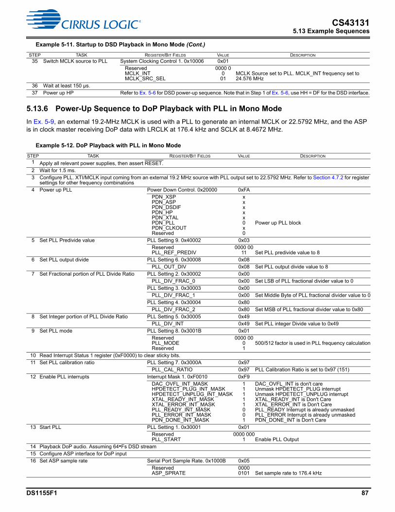
DS1155F1 87
CS431315.13 Example Sequences
5.13.6 Power-Up Sequence to DoP Playback with PLL in Mono Mode
In Ex. 5-9, an external 19.2-MHz MCLK is used with a PLL to generate an internal MCLK or 22.5792 MHz, and the ASP is in clock master receiving DoP data with LRCLK at 176.4 kHz and SCLK at 8.4672 MHz.
35 Switch MCLK source to PLL System Clocking Control 1. 0x10006 0x01ReservedMCLK_INTMCLK_SRC_SEL
0000 0001
MCLK Source set to PLL. MCLK_INT frequency set to 24.576 MHz
36 Wait at least 150 µs.37 Power up HP Refer to Ex. 5-6 for DSD power-up sequence. Note that in Step 1 of Ex. 5-6, use HH = DF for the DSD interface.
Example 5-12. DoP Playback with PLL in Mono Mode
STEP TASK REGISTER/BIT FIELDS VALUE DESCRIPTION
1 Apply all relevant power supplies, then assert RESET.2 Wait for 1.5 ms.3 Configure PLL. XTI/MCLK input coming from an external 19.2 MHz source with PLL output set to 22.5792 MHz. Refer to Section 4.7.2 for register
settings for other frequency combinations4 Power up PLL Power Down Control. 0x20000 0xFA
PDN_XSPPDN_ASPPDN_DSDIFPDN_HPPDN_XTALPDN_PLLPDN_CLKOUTReserved
xxxxx0x0
Power up PLL block
5 Set PLL Predivide value PLL Setting 9. 0x40002 0x03ReservedPLL_REF_PREDIV
0000 0011 Set PLL predivide value to 8
6 Set PLL output divide PLL Setting 6. 0x30008 0x08PLL_OUT_DIV 0x08 Set PLL output divide value to 8
7 Set Fractional portion of PLL Divide Ratio PLL Setting 2. 0x30002 0x00PLL_DIV_FRAC_0 0x00 Set LSB of PLL fractional divider value to 0
PLL Setting 3. 0x30003 0x00PLL_DIV_FRAC_1 0x00 Set Middle Byte of PLL fractional divider value to 0
PLL Setting 4. 0x30004 0x80PLL_DIV_FRAC_2 0x80 Set MSB of PLL fractional divider value to 0x80
8 Set Integer portion of PLL Divide Ratio PLL Setting 5. 0x30005 0x49PLL_DIV_INT 0x49 Set PLL integer Divide value to 0x49
9 Set PLL mode PLL Setting 8. 0x3001B 0x01ReservedPLL_MODEReserved
0000 0001
500/512 factor is used in PLL frequency calculation
10 Read Interrupt Status 1 register (0xF0000) to clear sticky bits.11 Set PLL calibration ratio PLL Setting 7. 0x3000A 0x97
PLL_CAL_RATIO 0x97 PLL Calibration Ratio is set to 0x97 (151)12 Enable PLL interrupts Interrupt Mask 1. 0xF0010 0xF9
DAC_OVFL_INT_MASKHPDETECT_PLUG_INT_MASKHPDETECT_UNPLUG_INT_MASKXTAL_READY_INT_MASKXTAL_ERROR_INT_MASKPLL_READY_INT_MASKPLL_ERROR_INT_MASKPDN_DONE_INT_MASK
11111001
DAC_OVFL_INT is don't careUnmask HPDETECT_PLUG interruptUnmask HPDETECT_UNPLUG interruptXTAL_READY_INT is Don't CareXTAL_ERROR_INT is Don't CarePLL_READY Interrupt is already unmaskedPLL_ERROR Interrupt is already unmaskedPDN_DONE_INT is Don't Care
13 Start PLL PLL Setting 1. 0x30001 0x01ReservedPLL_START
0000 0001 Enable PLL Output
14 Playback DoP audio. Assuming 64•Fs DSD stream15 Configure ASP interface for DoP input16 Set ASP sample rate Serial Port Sample Rate. 0x1000B 0x05
ReservedASP_SPRATE
00000101 Set sample rate to 176.4 kHz
Example 5-11. Startup to DSD Playback in Mono Mode (Cont.)
STEP TASK REGISTER/BIT FIELDS VALUE DESCRIPTION
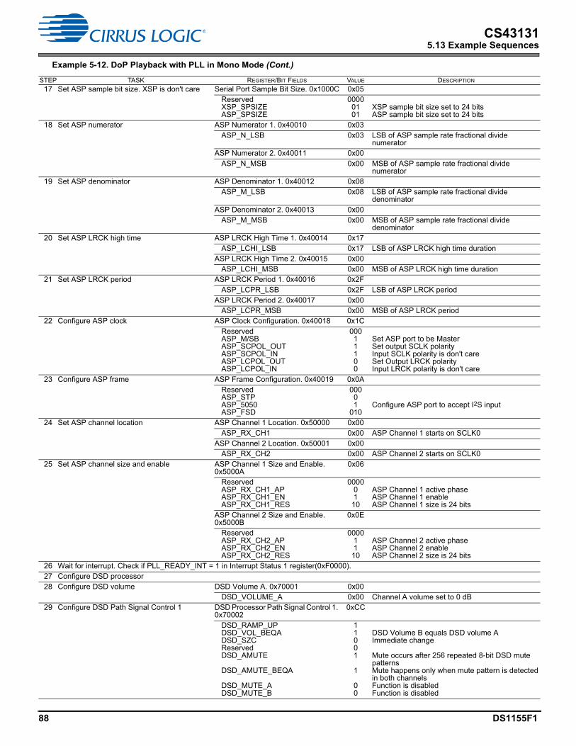
88 DS1155F1
CS431315.13 Example Sequences
17 Set ASP sample bit size. XSP is don't care Serial Port Sample Bit Size. 0x1000C 0x05ReservedXSP_SPSIZEASP_SPSIZE
00000101
XSP sample bit size set to 24 bitsASP sample bit size set to 24 bits
18 Set ASP numerator ASP Numerator 1. 0x40010 0x03ASP_N_LSB 0x03 LSB of ASP sample rate fractional divide
numeratorASP Numerator 2. 0x40011 0x00
ASP_N_MSB 0x00 MSB of ASP sample rate fractional divide numerator
19 Set ASP denominator ASP Denominator 1. 0x40012 0x08ASP_M_LSB 0x08 LSB of ASP sample rate fractional divide
denominatorASP Denominator 2. 0x40013 0x00
ASP_M_MSB 0x00 MSB of ASP sample rate fractional divide denominator
20 Set ASP LRCK high time ASP LRCK High Time 1. 0x40014 0x17ASP_LCHI_LSB 0x17 LSB of ASP LRCK high time duration
ASP LRCK High Time 2. 0x40015 0x00ASP_LCHI_MSB 0x00 MSB of ASP LRCK high time duration
21 Set ASP LRCK period ASP LRCK Period 1. 0x40016 0x2FASP_LCPR_LSB 0x2F LSB of ASP LRCK period
ASP LRCK Period 2. 0x40017 0x00ASP_LCPR_MSB 0x00 MSB of ASP LRCK period
22 Configure ASP clock ASP Clock Configuration. 0x40018 0x1CReservedASP_M/SBASP_SCPOL_OUTASP_SCPOL_INASP_LCPOL_OUTASP_LCPOL_IN
00011100
Set ASP port to be MasterSet output SCLK polarityInput SCLK polarity is don't careSet Output LRCK polarityInput LRCK polarity is don't care
23 Configure ASP frame ASP Frame Configuration. 0x40019 0x0AReservedASP_STPASP_5050ASP_FSD
00001
010Configure ASP port to accept I2S input
24 Set ASP channel location ASP Channel 1 Location. 0x50000 0x00ASP_RX_CH1 0x00 ASP Channel 1 starts on SCLK0
ASP Channel 2 Location. 0x50001 0x00ASP_RX_CH2 0x00 ASP Channel 2 starts on SCLK0
25 Set ASP channel size and enable ASP Channel 1 Size and Enable. 0x5000A
0x06
ReservedASP_RX_CH1_APASP_RX_CH1_ENASP_RX_CH1_RES
00000110
ASP Channel 1 active phaseASP Channel 1 enableASP Channel 1 size is 24 bits
ASP Channel 2 Size and Enable. 0x5000B
0x0E
ReservedASP_RX_CH2_APASP_RX_CH2_ENASP_RX_CH2_RES
00001110
ASP Channel 2 active phaseASP Channel 2 enableASP Channel 2 size is 24 bits
26 Wait for interrupt. Check if PLL_READY_INT = 1 in Interrupt Status 1 register(0xF0000).27 Configure DSD processor28 Configure DSD volume DSD Volume A. 0x70001 0x00
DSD_VOLUME_A 0x00 Channel A volume set to 0 dB29 Configure DSD Path Signal Control 1 DSD Processor Path Signal Control 1.
0x700020xCC
DSD_RAMP_UPDSD_VOL_BEQADSD_SZCReservedDSD_AMUTE
DSD_AMUTE_BEQA
DSD_MUTE_ADSD_MUTE_B
11001
1
00
DSD Volume B equals DSD volume AImmediate change
Mute occurs after 256 repeated 8-bit DSD mute patternsMute happens only when mute pattern is detected in both channelsFunction is disabledFunction is disabled
Example 5-12. DoP Playback with PLL in Mono Mode (Cont.)
STEP TASK REGISTER/BIT FIELDS VALUE DESCRIPTION

DS1155F1 89
CS431315.13 Example Sequences
30 Configure DSD interface DSD Interface Configuration. 0x70003
0x04
ReservedDSD_M/SBDSD_PM_ENDSD_PM_SEL
0000 0100
DSD is clock masterFunction is disabledFunction is disabled
31 Configure DSD Path Signal Control 2 DSD Processor Path Signal Control 2. 0x70004
0x50
ReservedDSD_PRC_SRCDSD_ENReservedDSD_SPEEDSTA_DSD_DETINV_DSD_DET
01010000
Set source of DSD processor to ASPEnable DSD playback
Set DSD clock speed to 64•FsStatic DSD detection disabledInvalid DSD detection disabled
32 Configure DSD path Signal Control 3. Enable mono mode:a. Select Channel A/B (DSD_SWAP_CHAN)b. Copy Channel A to B (DSD_COPY_CHAN)c. Invert Channel B (DSD_INV_B)
DSD Processor Path Signal Control 3. 0x70006
0xC5/0xC7 for Left/Right channel
DSD_ZERODB
DSD_HPF_ENReservedSIGCTL_DSDEQPCMDSD_INV_ADSD_INV_BDSD_SWAP_CHANDSD_COPY_CHAN
1
10001
0/11
The SACD 0–dB reference level (50%modulation index) matches PCM 0-dB full scale.Enable HPF in DSD processor
Function is disabledFunction is disabledFunction is enabledFunction is enabled/disabledFunction is enabled
33 Configure headphone output for 1.732 V rms34 Configure Class H amplifier Class H Control. 0xB0000 0x1E
ReservedADPT_PWRHV_ENEXT_VCPFILT
0001 11
10
Output signal determines voltage levelHigh voltage mode enabled Using internal VCPFILT source.
35 Set HP output to full scale HP Output Control 1. 0x80000 0x30HP_CLAMPA HP_CLAMPB OUT_FSHP_IN_EN HP_IN_LP Reserved+1dB_EN
00110000
Set headphone output to full scale (1.732 V rms)
36 Headphone detect HP Detect. 0xD0000 0xC4HPDETECT_CTRLHPDETECT_INVHPDETECT_RISE_DBC_TIMEHPDETECT_FALL_DBC_TIMEReserved
110
0 0100
HP detect enabledHP detect input is not invertedTip Sense rising debounce time set to 0 msTip sense falling debounce time set to 500 ms
37 Enable interrupts38 Read Interrupt Status 1 register (0xF0000), Interrupt Status 2 register (0xF0001) and Interrupt Status 5 register (0xF0004) to clear sticky bits.39 Enable headphone detect interrupts Interrupt Mask 1. 0xF0010 0x99
DAC_OVFL_INT_MASKHPDETECT_PLUG_INT_MASKHPDETECT_UNPLUG_INT_MASKXTAL_READY_INT_MASKXTAL_ERROR_INT_MASKPLL_READY_INT_MASKPLL_ERROR_INT_MASKPDN_DONE_INT_MASK
10011001
DAC_OVFL_INT is don't careEnable HPDETECT_PLUG interruptEnable HPDETECT_UNPLUG interruptXTAL_READY_INT is don't careXTAL_ERROR_INT is don't carePLL_READY interrupt already enabledPLL_ERROR interrupt already enabledPDN_DONE_INT is don't care
40 Enable ASP interrupts Interrupt Mask 2. 0xF0011 0x07ASP_OVFL_INT_MASKASP_ERROR_INT_MASKASP_LATE_INT_MASKASP_EARLY_INT_MASKASP_NOLRCK_INT_MASKReserved
00000
111
Enable ASP_OVFL interruptEnable ASP_ERROR interruptEnable ASP_LATE interruptEnable ASP_EARLY interruptEnable ASP_NOLRCK interrupt
41 Enable DSD and DoP interrupts Interrupt Mask 5. 0xF0014 0x01DSD_STUCK_INT_MASKDSD_INVAL_A_INT_MASKDSD_INVAL_B_INT_MASKDSD_SILENCE_A_INT_MASKDSD_SILENCE_B_INT_MASKDSD_RATE_ERROR_INT_MASKDOP_MRK_DET_INT_MASKDOP_ON_INT_MASK
00000001
Enable DSD_STUCK interruptEnable DSD_INVAL_A interruptEnable DSD_INVAL_B interruptEnable DSD_SILENCE_A interruptEnable DSD_SILENCE_B interruptEnable DSD_RATE_ERROR interruptEnable DOP_MRK_DET interruptDisable DOP_ON interrupt
Example 5-12. DoP Playback with PLL in Mono Mode (Cont.)
STEP TASK REGISTER/BIT FIELDS VALUE DESCRIPTION
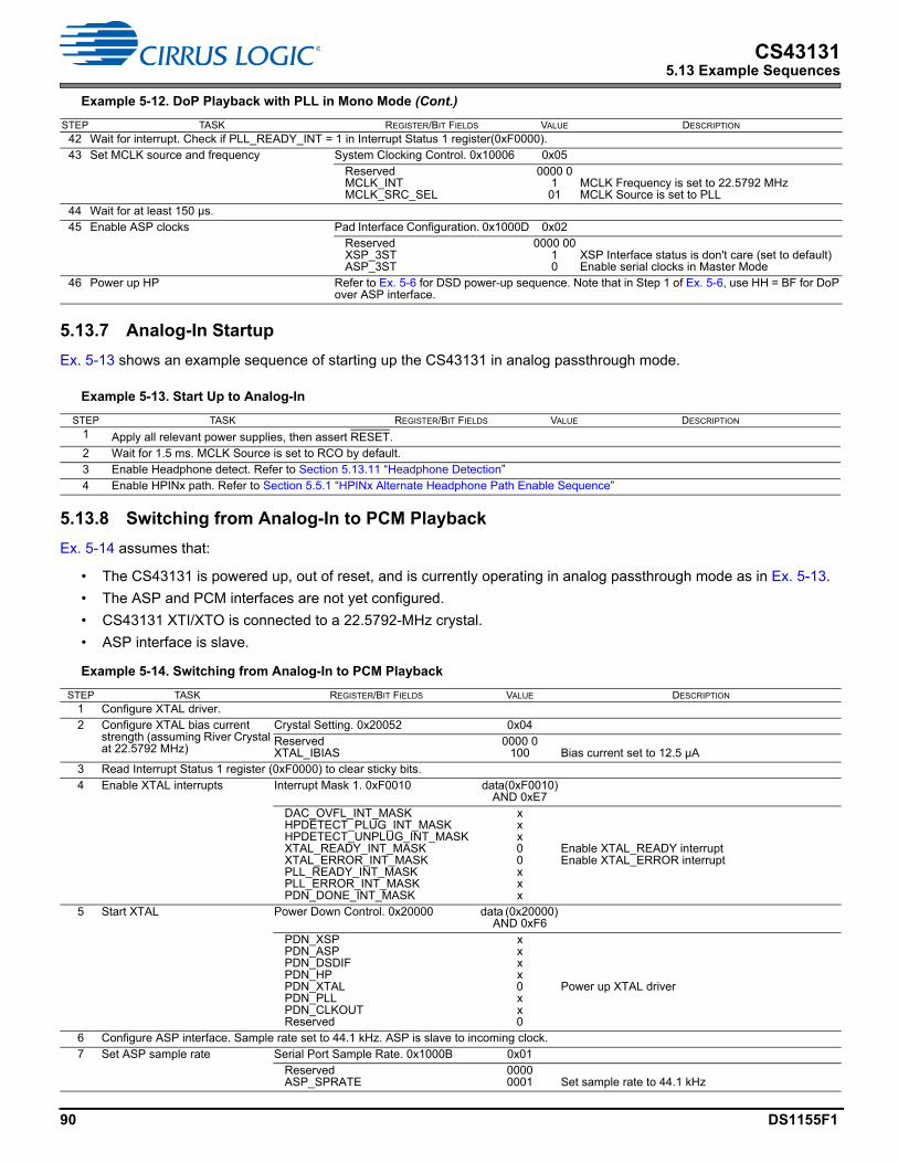
90 DS1155F1
CS431315.13 Example Sequences
5.13.7 Analog-In Startup
Ex. 5-13 shows an example sequence of starting up the CS43131 in analog passthrough mode.
5.13.8 Switching from Analog-In to PCM Playback
Ex. 5-14 assumes that:
• The CS43131 is powered up, out of reset, and is currently operating in analog passthrough mode as in Ex. 5-13.
• The ASP and PCM interfaces are not yet configured.
• CS43131 XTI/XTO is connected to a 22.5792-MHz crystal.
• ASP interface is slave.
42 Wait for interrupt. Check if PLL_READY_INT = 1 in Interrupt Status 1 register(0xF0000).43 Set MCLK source and frequency System Clocking Control. 0x10006 0x05
ReservedMCLK_INTMCLK_SRC_SEL
0000 0101
MCLK Frequency is set to 22.5792 MHzMCLK Source is set to PLL
44 Wait for at least 150 µs.45 Enable ASP clocks Pad Interface Configuration. 0x1000D 0x02
ReservedXSP_3STASP_3ST
0000 0010
XSP Interface status is don't care (set to default)Enable serial clocks in Master Mode
46 Power up HP Refer to Ex. 5-6 for DSD power-up sequence. Note that in Step 1 of Ex. 5-6, use HH = BF for DoP over ASP interface.
Example 5-13. Start Up to Analog-In
STEP TASK REGISTER/BIT FIELDS VALUE DESCRIPTION
1 Apply all relevant power supplies, then assert RESET.2 Wait for 1.5 ms. MCLK Source is set to RCO by default.3 Enable Headphone detect. Refer to Section 5.13.11 “Headphone Detection”4 Enable HPINx path. Refer to Section 5.5.1 “HPINx Alternate Headphone Path Enable Sequence”
Example 5-14. Switching from Analog-In to PCM Playback
STEP TASK REGISTER/BIT FIELDS VALUE DESCRIPTION
1 Configure XTAL driver.2 Configure XTAL bias current
strength (assuming River Crystal at 22.5792 MHz)
Crystal Setting. 0x20052 0x04ReservedXTAL_IBIAS
0000 0100 Bias current set to 12.5 µA
3 Read Interrupt Status 1 register (0xF0000) to clear sticky bits.4 Enable XTAL interrupts Interrupt Mask 1. 0xF0010 data(0xF0010)
AND 0xE7DAC_OVFL_INT_MASKHPDETECT_PLUG_INT_MASKHPDETECT_UNPLUG_INT_MASKXTAL_READY_INT_MASKXTAL_ERROR_INT_MASKPLL_READY_INT_MASKPLL_ERROR_INT_MASKPDN_DONE_INT_MASK
xxx00xxx
Enable XTAL_READY interruptEnable XTAL_ERROR interrupt
5 Start XTAL Power Down Control. 0x20000 data (0x20000) AND 0xF6
PDN_XSPPDN_ASPPDN_DSDIFPDN_HPPDN_XTALPDN_PLLPDN_CLKOUTReserved
xxxx0xx0
Power up XTAL driver
6 Configure ASP interface. Sample rate set to 44.1 kHz. ASP is slave to incoming clock.7 Set ASP sample rate Serial Port Sample Rate. 0x1000B 0x01
ReservedASP_SPRATE
00000001 Set sample rate to 44.1 kHz
Example 5-12. DoP Playback with PLL in Mono Mode (Cont.)
STEP TASK REGISTER/BIT FIELDS VALUE DESCRIPTION
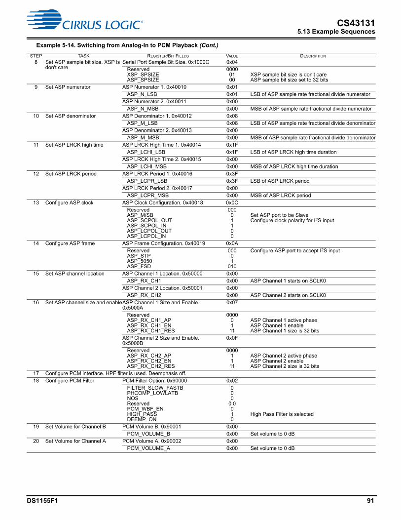
DS1155F1 91
CS431315.13 Example Sequences
8 Set ASP sample bit size. XSP is don't care
Serial Port Sample Bit Size. 0x1000C 0x04ReservedXSP_SPSIZEASP_SPSIZE
00000100
XSP sample bit size is don't careASP sample bit size set to 32 bits
9 Set ASP numerator ASP Numerator 1. 0x40010 0x01ASP_N_LSB 0x01 LSB of ASP sample rate fractional divide numerator
ASP Numerator 2. 0x40011 0x00ASP_N_MSB 0x00 MSB of ASP sample rate fractional divide numerator
10 Set ASP denominator ASP Denominator 1. 0x40012 0x08ASP_M_LSB 0x08 LSB of ASP sample rate fractional divide denominator
ASP Denominator 2. 0x40013 0x00ASP_M_MSB 0x00 MSB of ASP sample rate fractional divide denominator
11 Set ASP LRCK high time ASP LRCK High Time 1. 0x40014 0x1FASP_LCHI_LSB 0x1F LSB of ASP LRCK high time duration
ASP LRCK High Time 2. 0x40015 0x00ASP_LCHI_MSB 0x00 MSB of ASP LRCK high time duration
12 Set ASP LRCK period ASP LRCK Period 1. 0x40016 0x3FASP_LCPR_LSB 0x3F LSB of ASP LRCK period
ASP LRCK Period 2. 0x40017 0x00ASP_LCPR_MSB 0x00 MSB of ASP LRCK period
13 Configure ASP clock ASP Clock Configuration. 0x40018 0x0CReservedASP_M/SBASP_SCPOL_OUTASP_SCPOL_INASP_LCPOL_OUTASP_LCPOL_IN
00001100
Set ASP port to be SlaveConfigure clock polarity for I2S input
14 Configure ASP frame ASP Frame Configuration. 0x40019 0x0AReservedASP_STPASP_5050ASP_FSD
00001
010
Configure ASP port to accept I2S input
15 Set ASP channel location ASP Channel 1 Location. 0x50000 0x00ASP_RX_CH1 0x00 ASP Channel 1 starts on SCLK0
ASP Channel 2 Location. 0x50001 0x00ASP_RX_CH2 0x00 ASP Channel 2 starts on SCLK0
16 Set ASP channel size and enableASP Channel 1 Size and Enable. 0x5000A
0x07
ReservedASP_RX_CH1_APASP_RX_CH1_ENASP_RX_CH1_RES
00000111
ASP Channel 1 active phaseASP Channel 1 enableASP Channel 1 size is 32 bits
ASP Channel 2 Size and Enable. 0x5000B
0x0F
ReservedASP_RX_CH2_APASP_RX_CH2_ENASP_RX_CH2_RES
00001111
ASP Channel 2 active phaseASP Channel 2 enableASP Channel 2 size is 32 bits
17 Configure PCM interface. HPF filter is used. Deemphasis off.18 Configure PCM Filter PCM Filter Option. 0x90000 0x02
FILTER_SLOW_FASTBPHCOMP_LOWLATBNOSReservedPCM_WBF_ENHIGH_PASSDEEMP_ON
000
0 0010
High Pass Filter is selected
19 Set Volume for Channel B PCM Volume B. 0x90001 0x00PCM_VOLUME_B 0x00 Set volume to 0 dB
20 Set Volume for Channel A PCM Volume A. 0x90002 0x00PCM_VOLUME_A 0x00 Set volume to 0 dB
Example 5-14. Switching from Analog-In to PCM Playback (Cont.)
STEP TASK REGISTER/BIT FIELDS VALUE DESCRIPTION

92 DS1155F1
CS431315.13 Example Sequences
21 Configure PCM Path Signal Control
PCM Path Signal Control 1. 0x90003 0xECPCM_RAMP_DOWNPCM_VOL_BEQA
PCM_SZCPCM_AMUTEPCM_AMUTEBEQA
PCM_MUTE_APCM_MUTE_B
11
1011
00
Soft ramp down of volume on filter changeVolume setting on both channels controlled by PCM_VOLUME_AEnable soft rampMute after reception of 8192 samples of 0 or –1.Mute only when AMUTE condition is detected on both channelsFunction is disabledFunction is disabled
PCM Path Signal Control 2. 0x90004 0x00ReservedPCM_INV_APCM_INV_BPCM_SWAP_CHANPCM_COPY_CHAN
00000000
Disable all functions in this register
22 Configure HP interface23 Configure Class H Amplifier Class H Control. 0xB0000 0x1E
ReservedADPT_PWRHV_ENEXT_VCPFILT
0001 11
10
Output signal determines voltage levelHigh voltage mode enabled Using Internal VCPFILT source.
24 Headphone Detect HP Detect. 0xD0000 0xC4HPDETECT_CTRLHPDETECT_INVHPDETECT_RISE_DBC_TIMEHPDETECT_FALL_DBC_TIMEReserved
110
0 0100
HP Detect enabledHP detect input is not invertedTip Sense rising debounce time set to 0 msTip sense falling debounce time set to 500 ms
25 Enable interrupts26 Read Interrupt Status 1 register (0xF0000) and Interrupt Status 2 register (0xF0001) to clear sticky bits.27 Enable headphone detect
interruptsInterrupt Mask 1. 0xF0010 data(0xF0010)
AND 0x9FDAC_OVFL_INT_MASKHPDETECT_PLUG_INT_MASKHPDETECT_UNPLUG_INT_MASKXTAL_READY_INT_MASKXTAL_ERROR_INT_MASKPLL_READY_INT_MASKPLL_ERROR_INT_MASKPDN_DONE_INT_MASK
x00xxxxx
Enable HPDETECT_PLUG interruptEnable HPDETECT_UNPLUG interrupt
28 Enable ASP interrupts Interrupt Mask 2. 0xF0011 0x07ASP_OVFL_INT_MASKASP_ERROR_INT_MASKASP_LATE_INT_MASKASP_EARLY_INT_MASKASP_NOLRCK_INT_MASKReserved
00000
111
Enable ASP_OVFL interruptEnable ASP_ERROR interruptEnable ASP_LATE interruptEnable ASP_EARLY interruptEnable ASP_NOLRCK interrupt
29 Initiate a soft ramp down of HPINx input to mute.30 Disable HPINx Refer to Section 5.5.231 Wait for interrupt. Check if XTAL_READY_INT = 1 in Interrupt Status 1 register(0xF0000).32 Switch MCLK source to XTAL System Clocking Control 1. 0x10006 0x04
ReservedMCLK_INTMCLK_SRC_SEL
0000 0100
MCLK Source set to XTAL. MCLK_INT frequency set to 22.5792MHz
33 Wait at least 150 µs.34 Power up ASP Power Down Control. 0x20000 0xB6
PDN_XSPPDN_ASPPDN_DSDIFPDN_HPPDN_XTALPDN_PLLPDN_CLKOUTReserved
10110110
Enable ASP data pinsXTAL is already enabled
35 Power up HP Refer to Ex. 5-5 for PCM power-up sequence
Example 5-14. Switching from Analog-In to PCM Playback (Cont.)
STEP TASK REGISTER/BIT FIELDS VALUE DESCRIPTION
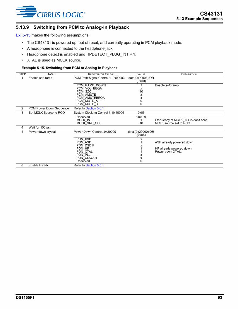
DS1155F1 93
CS431315.13 Example Sequences
5.13.9 Switching from PCM to Analog-In Playback
Ex. 5-15 makes the following assumptions:
• The CS43131 is powered up, out of reset, and currently operating in PCM playback mode.
• A headphone is connected to the headphone jack.
• Headphone detect is enabled and HPDETECT_PLUG_INT = 1.
• XTAL is used as MCLK source.
Example 5-15. Switching from PCM to Analog-In Playback
STEP TASK REGISTER/BIT FIELDS VALUE DESCRIPTION
1 Enable soft ramp PCM Path Signal Control 1. 0x90003 data(0x90003) OR (0xA0)
PCM_RAMP_DOWNPCM_VOL_BEQAPCM_SZCPCM_AMUTEPCM_AMUTEBEQAPCM_MUTE_APCM_MUTE_B
1x
10xx00
Enable soft ramp
2 PCM Power Down Sequence Refer to Section 5.6.13 Set MCLK Source to RCO System Clocking Control 1. 0x10006 0x06
ReservedMCLK_INTMCLK_SRC_SEL
0000 0110
Frequency of MCLK_INT is don't careMCLK source set to RCO
4 Wait for 150 µs.5 Power down crystal Power Down Control. 0x20000 data (0x20000) OR
(0x08)PDN_XSPPDN_ASPPDN_DSDIFPDN_HPPDN_XTALPDN_PLLPDN_CLKOUTReserved
x1x11xx0
ASP already powered down
HP already powered downPower down XTAL.
6 Enable HPINx Refer to Section 5.5.1
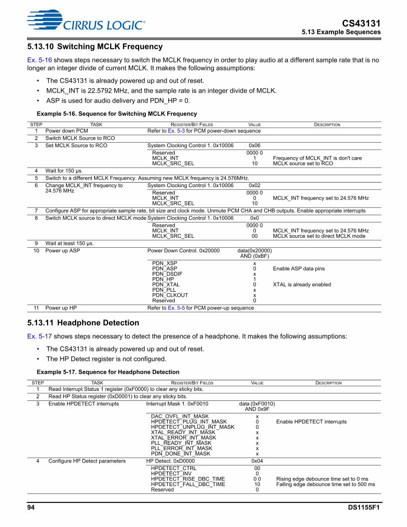
94 DS1155F1
CS431315.13 Example Sequences
5.13.10 Switching MCLK Frequency
Ex. 5-16 shows steps necessary to switch the MCLK frequency in order to play audio at a different sample rate that is no longer an integer divide of current MCLK. It makes the following assumptions:
• The CS43131 is already powered up and out of reset.
• MCLK_INT is 22.5792 MHz, and the sample rate is an integer divide of MCLK.
• ASP is used for audio delivery and PDN_HP = 0.
5.13.11 Headphone Detection
Ex. 5-17 shows steps necessary to detect the presence of a headphone. It makes the following assumptions:
• The CS43131 is already powered up and out of reset.
• The HP Detect register is not configured.
Example 5-16. Sequence for Switching MCLK Frequency
STEP TASK REGISTER/BIT FIELDS VALUE DESCRIPTION
1 Power down PCM Refer to Ex. 5-3 for PCM power-down sequence2 Switch MCLK Source to RCO3 Set MCLK Source to RCO System Clocking Control 1. 0x10006 0x06
ReservedMCLK_INTMCLK_SRC_SEL
0000 0110
Frequency of MCLK_INT is don't careMCLK source set to RCO
4 Wait for 150 µs.5 Switch to a different MCLK Frequency. Assuming new MCLK frequency is 24.576MHz.6 Change MCLK_INT frequency to
24.576 MHzSystem Clocking Control 1. 0x10006 0x02
ReservedMCLK_INTMCLK_SRC_SEL
0000 0010
MCLK_INT frequency set to 24.576 MHz
7 Configure ASP for appropriate sample rate, bit size and clock mode. Unmute PCM CHA and CHB outputs. Enable appropriate interrupts8 Switch MCLK source to direct MCLK mode System Clocking Control 1. 0x10006 0x0
ReservedMCLK_INTMCLK_SRC_SEL
0000 0000
MCLK_INT frequency set to 24.576 MHzMCLK source set to direct MCLK mode
9 Wait at least 150 µs.10 Power up ASP Power Down Control. 0x20000 data(0x20000)
AND (0xBF)PDN_XSPPDN_ASPPDN_DSDIFPDN_HPPDN_XTALPDN_PLLPDN_CLKOUTReserved
x0x10xx0
Enable ASP data pins
XTAL is already enabled
11 Power up HP Refer to Ex. 5-5 for PCM power-up sequence
Example 5-17. Sequence for Headphone Detection
STEP TASK REGISTER/BIT FIELDS VALUE DESCRIPTION
1 Read Interrupt Status 1 register (0xF0000) to clear any sticky bits.2 Read HP Status register (0xD0001) to clear any sticky bits.3 Enable HPDETECT interrupts Interrupt Mask 1. 0xF0010 data (0xF0010)
AND 0x9FDAC_OVFL_INT_MASKHPDETECT_PLUG_INT_MASKHPDETECT_UNPLUG_INT_MASKXTAL_READY_INT_MASKXTAL_ERROR_INT_MASKPLL_READY_INT_MASKPLL_ERROR_INT_MASKPDN_DONE_INT_MASK
x00xxxxx
Enable HPDETECT interrupts
4 Configure HP Detect parameters HP Detect. 0xD0000 0x04HPDETECT_CTRLHPDETECT_INVHPDETECT_RISE_DBC_TIMEHPDETECT_FALL_DBC_TIMEReserved
000
0 0100
Rising edge debounce time set to 0 msFalling edge debounce time set to 500 ms
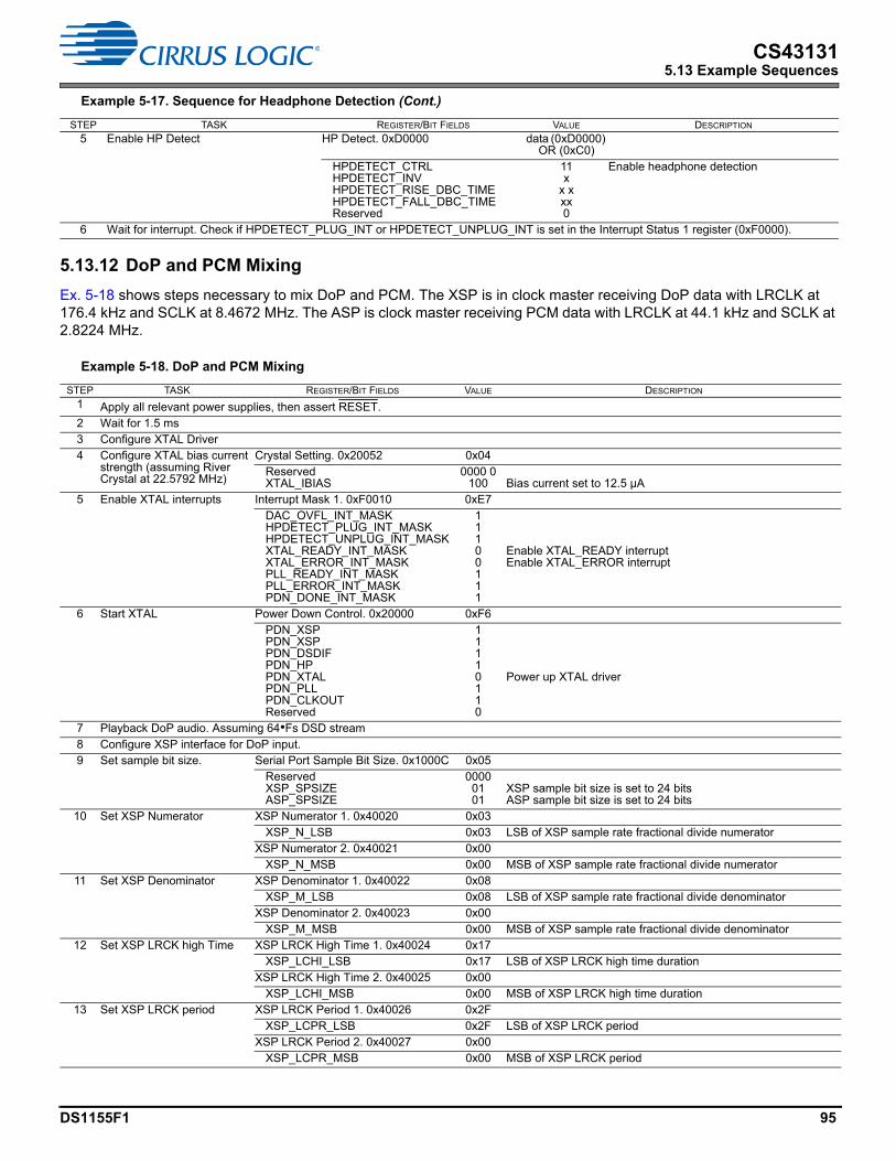
DS1155F1 95
CS431315.13 Example Sequences
5.13.12 DoP and PCM Mixing
Ex. 5-18 shows steps necessary to mix DoP and PCM. The XSP is in clock master receiving DoP data with LRCLK at 176.4 kHz and SCLK at 8.4672 MHz. The ASP is clock master receiving PCM data with LRCLK at 44.1 kHz and SCLK at 2.8224 MHz.
5 Enable HP Detect HP Detect. 0xD0000 data (0xD0000) OR (0xC0)
HPDETECT_CTRLHPDETECT_INVHPDETECT_RISE_DBC_TIMEHPDETECT_FALL_DBC_TIMEReserved
11x
x xxx0
Enable headphone detection
6 Wait for interrupt. Check if HPDETECT_PLUG_INT or HPDETECT_UNPLUG_INT is set in the Interrupt Status 1 register (0xF0000).
Example 5-18. DoP and PCM Mixing
STEP TASK REGISTER/BIT FIELDS VALUE DESCRIPTION
1 Apply all relevant power supplies, then assert RESET.2 Wait for 1.5 ms3 Configure XTAL Driver4 Configure XTAL bias current
strength (assuming River Crystal at 22.5792 MHz)
Crystal Setting. 0x20052 0x04ReservedXTAL_IBIAS
0000 0100 Bias current set to 12.5 µA
5 Enable XTAL interrupts Interrupt Mask 1. 0xF0010 0xE7DAC_OVFL_INT_MASKHPDETECT_PLUG_INT_MASKHPDETECT_UNPLUG_INT_MASKXTAL_READY_INT_MASKXTAL_ERROR_INT_MASKPLL_READY_INT_MASKPLL_ERROR_INT_MASKPDN_DONE_INT_MASK
11100111
Enable XTAL_READY interruptEnable XTAL_ERROR interrupt
6 Start XTAL Power Down Control. 0x20000 0xF6PDN_XSPPDN_XSPPDN_DSDIFPDN_HPPDN_XTALPDN_PLLPDN_CLKOUTReserved
11110110
Power up XTAL driver
7 Playback DoP audio. Assuming 64•Fs DSD stream8 Configure XSP interface for DoP input. 9 Set sample bit size. Serial Port Sample Bit Size. 0x1000C 0x05
ReservedXSP_SPSIZEASP_SPSIZE
00000101
XSP sample bit size is set to 24 bitsASP sample bit size is set to 24 bits
10 Set XSP Numerator XSP Numerator 1. 0x40020 0x03XSP_N_LSB 0x03 LSB of XSP sample rate fractional divide numerator
XSP Numerator 2. 0x40021 0x00XSP_N_MSB 0x00 MSB of XSP sample rate fractional divide numerator
11 Set XSP Denominator XSP Denominator 1. 0x40022 0x08XSP_M_LSB 0x08 LSB of XSP sample rate fractional divide denominator
XSP Denominator 2. 0x40023 0x00XSP_M_MSB 0x00 MSB of XSP sample rate fractional divide denominator
12 Set XSP LRCK high Time XSP LRCK High Time 1. 0x40024 0x17XSP_LCHI_LSB 0x17 LSB of XSP LRCK high time duration
XSP LRCK High Time 2. 0x40025 0x00XSP_LCHI_MSB 0x00 MSB of XSP LRCK high time duration
13 Set XSP LRCK period XSP LRCK Period 1. 0x40026 0x2FXSP_LCPR_LSB 0x2F LSB of XSP LRCK period
XSP LRCK Period 2. 0x40027 0x00XSP_LCPR_MSB 0x00 MSB of XSP LRCK period
Example 5-17. Sequence for Headphone Detection (Cont.)
STEP TASK REGISTER/BIT FIELDS VALUE DESCRIPTION

96 DS1155F1
CS431315.13 Example Sequences
14 Configure XSP Clock XSP Clock Configuration. 0x40028 0x1CReservedXSP_M/SBXSP_SCPOL_OUTXSP_SCPOL_INXSP_LCPOL_OUTXSP_LCPOL_IN
00011100
Set XSP port to be MasterSet output SCLK polarityInput SCLK polarity is don’t careSet Output LRCLK polarityInput LRCLK polarity is don’t care
15 Configure XSP Frame XSP Frame Configuration. 0x40029 0x0AReservedXSP_STPXSP_5050XSP_FSD
00001
010
Configure XSP port to accept I2S input
16 Set XSP Channel Location XSP Channel 1 Location. 0x60000 0x00XSP_RX_CH1 0x00 XSP Channel 1 starts on SCLK0
XSP Channel 2 Location. 0x60001 0x00XSP_RX_CH2 0x00 XSP Channel 2 starts on SCLK0
17 Set XSP Channel Size and Enable
XSP Channel 1 Size and Enable. 0x6000A
0x06
ReservedXSP_RX_CH1_APXSP_RX_CH1_ENXSP_RX_CH1_RES
00000110
XSP Channel 1 Active PhaseXSP Channel 1 EnableXSP Channel 1 Size is 24 bits
XSP Channel 2 Size and Enable. 0x6000B
0x0E
ReservedXSP_RX_CH2_APXSP_RX_CH2_ENXSP_RX_CH2_RES
00001110
XSP Channel 2 Active PhaseXSP Channel 2 EnableXSP Channel 2 Size is 24 bits
18 Configure DSD Processor19 Configure DSD Volume DSD Volume A. 0x70001 0x00
DSD_VOLUME_A 0x00 Channel A volume set to 0 dB20 Configure DSD path Signal
Control 1DSD Processor Path Signal Control 1. 0x70002
0xCC
DSD_RAMP_UPDSD_VOL_BEQADSD_SZCReservedDSD_AMUTEDSD_AMUTE_BEQA
DSD_MUTE_ADSD_MUTE_B
110011
00
DSD Volume B equals DSD volume AImmediate change
Mute occurs after 256 repeated 8-bit DSD mute patternsMute happens only when mute pattern is detected in both channelsFunction is disabledFunction is disabled
21 Configure DSD Interface DSD Interface Configuration. 0x70003
0x00
ReservedDSD_M/SBDSD_PM_ENDSD_PM_SEL
0000 0000
DSD_M/SB is don’t careFunction is disabledFunction is disabled
22 Configure DSD path Signal Control 2
DSD Processor Path Signal Control 2. 0x70004
0x70
ReservedDSD_PRC_SRCDSD_ENReservedDSD_SPEEDSTA_DSD_DETINV_DSD_DET
01110000
Set source of DSD processor to XSPEnable DSD playback
Set DSD clock speed to 64•FSStatic DSD detection disabledInvalid DSD detection disabled
23 Configure DSD path Signal Control 3
DSD Processor Path Signal Control 3. 0x70006
0xC0
DSD_ZERODBDSD_HPF_ENReservedSIGCTL_DSDEQPCMDSD_INV_ADSD_INV_BDSD_SWAP_CHANDSD_COPY_CHAN
11000000
DSD stream volume settingEnable DSD HPF
Function is disabledFunction is disabledFunction is disabledFunction is disabledFunction is disabled
24 Configure HP Output for 1.732 Vrms
Example 5-18. DoP and PCM Mixing (Cont.)
STEP TASK REGISTER/BIT FIELDS VALUE DESCRIPTION
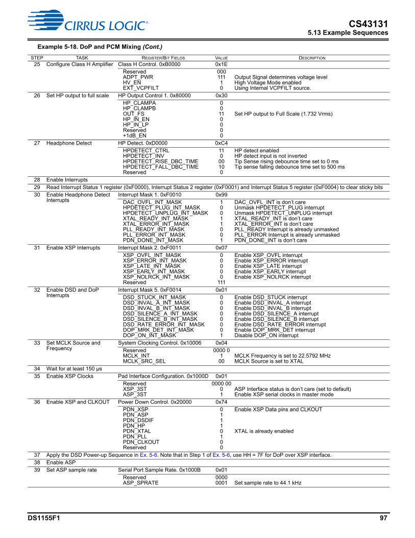
DS1155F1 97
CS431315.13 Example Sequences
25 Configure Class H Amplifier Class H Control. 0xB0000 0x1EReservedADPT_PWRHV_ENEXT_VCPFILT
00011110
Output Signal determines voltage levelHigh Voltage Mode enabledUsing Internal VCPFILT source.
26 Set HP output to full scale HP Output Control 1. 0x80000 0x30HP_CLAMPA HP_CLAMPB OUT_FSHP_IN_EN HP_IN_LP Reserved+1dB_EN
00110000
Set HP output to Full Scale (1.732 Vrms)
27 Headphone Detect HP Detect. 0xD0000 0xC4HPDETECT_CTRLHPDETECT_INVHPDETECT_RISE_DBC_TIMEHPDETECT_FALL_DBC_TIMEReserved
11000100
HP detect enabledHP detect input is not invertedTip Sense rising debounce time set to 0 msTip sense falling debounce time set to 500 ms
28 Enable Interrupts29 Read Interrupt Status 1 register (0xF0000), Interrupt Status 2 register (0xF0001) and Interrupt Status 5 register (0xF0004) to clear sticky bits30 Enable Headphone Detect
InterruptsInterrupt Mask 1. 0xF0010 0x99
DAC_OVFL_INT_MASKHPDETECT_PLUG_INT_MASKHPDETECT_UNPLUG_INT_MASKXTAL_READY_INT_MASKXTAL_ERROR_INT_MASKPLL_READY_INT_MASKPLL_ERROR_INT_MASKPDN_DONE_INT_MASK
10011001
DAC_OVFL_INT is don’t careUnmask HPDETECT_PLUG interruptUnmask HPDETECT_UNPLUG interruptXTAL_READY_INT is don’t careXTAL_ERROR_INT is don’t carePLL_READY Interrupt is already unmaskedPLL_ERROR Interrupt is already unmaskedPDN_DONE_INT is don’t care
31 Enable XSP Interrupts Interrupt Mask 2. 0xF0011 0x07XSP_OVFL_INT_MASKXSP_ERROR_INT_MASKXSP_LATE_INT_MASKXSP_EARLY_INT_MASKXSP_NOLRCK_INT_MASKReserved
00000
111
Enable XSP_OVFL interruptEnable XSP_ERROR interruptEnable XSP_LATE interruptEnable XSP_EARLY interruptEnable XSP_NOLRCK interrupt
32 Enable DSD and DoP Interrupts
Interrupt Mask 5. 0xF0014 0x01DSD_STUCK_INT_MASKDSD_INVAL_A_INT_MASKDSD_INVAL_B_INT_MASKDSD_SILENCE_A_INT_MASKDSD_SILENCE_B_INT_MASKDSD_RATE_ERROR_INT_MASKDOP_MRK_DET_INT_MASKDOP_ON_INT_MASK
00000001
Enable DSD_STUCK interruptEnable DSD_INVAL_A interruptEnable DSD_INVAL_B interruptEnable DSD_SILENCE_A interruptEnable DSD_SILENCE_B interruptEnable DSD_RATE_ERROR interruptEnable DOP_MRK_DET interruptDisable DOP_ON interrupt
33 Set MCLK Source and Frequency
System Clocking Control. 0x10006 0x04ReservedMCLK_INTMCLK_SRC_SEL
0000 0100
MCLK Frequency is set to 22.5792 MHzMCLK Source is set to XTAL
34 Wait for at least 150 µs35 Enable XSP Clocks Pad Interface Configuration. 0x1000D 0x01
ReservedXSP_3STASP_3ST
0000 0001
ASP Interface status is don’t care (set to default)Enable XSP serial clocks in master mode
36 Enable XSP and CLKOUT Power Down Control. 0x20000 0x74PDN_XSPPDN_ASPPDN_DSDIFPDN_HPPDN_XTALPDN_PLLPDN_CLKOUTReserved
01110100
Enable XSP Data pins and CLKOUT
XTAL is already enabled
37 Apply the DSD Power-up Sequence in Ex. 5-6. Note that in Step 1 of Ex. 5-6, use HH = 7F for DoP over XSP interface.38 Enable ASP39 Set ASP sample rate Serial Port Sample Rate. 0x1000B 0x01
ReservedASP_SPRATE
00000001 Set sample rate to 44.1 kHz
Example 5-18. DoP and PCM Mixing (Cont.)
STEP TASK REGISTER/BIT FIELDS VALUE DESCRIPTION

98 DS1155F1
CS431315.13 Example Sequences
40 Set ASP sample bit size Serial Port Sample Bit Size. 0x1000C 0x04ReservedXSP_SPSIZEASP_SPSIZE
00000100 ASP sample bit size set to 32 bits
41 Set ASP Numerator ASP Numerator 1. 0x40010 0x01ASP_N_LSB 0x01 LSB of ASP sample rate fractional divide numerator
ASP Numerator 2. 0x40011 0x00ASP_N_MSB 0x00 MSB of ASP sample rate fractional divide numerator
42 Set ASP Denominator ASP Denominator 1. 0x40012 0x08ASP_M_LSB 0x08 LSB of ASP sample rate fractional divide denominator
ASP Denominator 2. 0x40013 0x00ASP_M_MSB 0x00 MSB of ASP sample rate fractional divide denominator
43 Set ASP LRCK high Time ASP LRCK High Time 1. 0x40014 0x1FASP_LCHI_LSB 0x1F LSB of ASP LRCK high time duration
ASP LRCK High Time 2. 0x40015 0x00ASP_LCHI_MSB 0x00 MSB of ASP LRCK high time duration
44 Set ASP LRCK period ASP LRCK Period 1. 0x40016 0x3FASP_LCPR_LSB 0x3F LSB of ASP LRCK period
ASP LRCK Period 2. 0x40017 0x00ASP_LCPR_MSB 0x00 MSB of ASP LRCK period
45 Configure ASP Clock ASP Clock Configuration. 0x40018 0x1CReservedASP_M/SBASP_SCPOL_OUTASP_SCPOL_INASP_LCPOL_OUTASP_LCPOL_IN
00011100
Set ASP port to be MasterSet output SCLK polarityInput SCLK polarity is don’t careSet Output LRCLK polarityInput LRCLK polarity is don’t care
46 Configure ASP Frame ASP Frame Configuration. 0x40019 0x0AReservedASP_STPASP_5050ASP_FSD
00001
010
Configure ASP port to accept I2S input
47 Set ASP Channel Location ASP Channel 1 Location. 0x50000 0x00ASP_RX_CH1 0x00 ASP Channel 1 starts on SCLK0
ASP Channel 2 Location. 0x50001 0x00ASP_RX_CH2 0x00 ASP Channel 2 starts on SCLK0
48 Set ASP Channel Size and Enable
ASP Channel 1 Size and Enable. 0x5000A
0x07
ReservedASP_RX_CH1_APASP_RX_CH1_ENASP_RX_CH1_RES
00000111
ASP Channel 1 Active PhaseASP Channel 1 EnableASP Channel 1 Size is 32 bits
ASP Channel 2 Size and Enable. 0x5000B
0x0F
ReservedASP_RX_CH2_APASP_RX_CH2_ENASP_RX_CH2_RES
00001111
ASP Channel 2 Active PhaseASP Channel 2 EnableASP Channel 2 Size is 32 bits
49 Setup PCM50 Configure PCM Filter PCM Filter Option. 0x90000 0x02
FILTER_SLOW_FASTBPHCOMP_LOWLATBNOSReservedPCM_WBF_ENHIGH_PASSDEEMP_ON
000
0 0010
High Pass Filter is selected
51 Set Volume for Channel B PCM Volume B. 0x90001 0x0CPCM_VOLUME_B 0x0C Set volume to –6 dB
52 Set Volume for Channel A PCM Volume A. 0x90002 0x0CPCM_VOLUME_A 0x0C Set volume to –6 dB
Example 5-18. DoP and PCM Mixing (Cont.)
STEP TASK REGISTER/BIT FIELDS VALUE DESCRIPTION
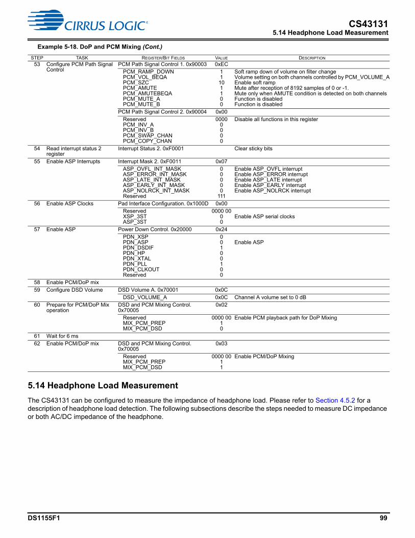
DS1155F1 99
CS431315.14 Headphone Load Measurement
5.14 Headphone Load Measurement
The CS43131 can be configured to measure the impedance of headphone load. Please refer to Section 4.5.2 for a description of headphone load detection. The following subsections describe the steps needed to measure DC impedance or both AC/DC impedance of the headphone.
53 Configure PCM Path Signal Control
PCM Path Signal Control 1. 0x90003 0xECPCM_RAMP_DOWNPCM_VOL_BEQAPCM_SZCPCM_AMUTEPCM_AMUTEBEQAPCM_MUTE_APCM_MUTE_B
11101100
Soft ramp down of volume on filter changeVolume setting on both channels controlled by PCM_VOLUME_AEnable soft rampMute after reception of 8192 samples of 0 or -1.Mute only when AMUTE condition is detected on both channelsFunction is disabledFunction is disabled
PCM Path Signal Control 2. 0x90004 0x00ReservedPCM_INV_APCM_INV_BPCM_SWAP_CHANPCM_COPY_CHAN
00000000
Disable all functions in this register
54 Read interrupt status 2 register
Interrupt Status 2. 0xF0001 Clear sticky bits
55 Enable ASP Interrupts Interrupt Mask 2. 0xF0011 0x07ASP_OVFL_INT_MASKASP_ERROR_INT_MASKASP_LATE_INT_MASKASP_EARLY_INT_MASKASP_NOLRCK_INT_MASKReserved
00000
111
Enable ASP_OVFL interruptEnable ASP_ERROR interruptEnable ASP_LATE interruptEnable ASP_EARLY interruptEnable ASP_NOLRCK interrupt
56 Enable ASP Clocks Pad Interface Configuration. 0x1000D 0x00ReservedXSP_3STASP_3ST
0000 0000
Enable ASP serial clocks
57 Enable ASP Power Down Control. 0x20000 0x24PDN_XSPPDN_ASPPDN_DSDIFPDN_HPPDN_XTALPDN_PLLPDN_CLKOUTReserved
00100100
Enable ASP
58 Enable PCM/DoP mix59 Configure DSD Volume DSD Volume A. 0x70001 0x0C
DSD_VOLUME_A 0x0C Channel A volume set to 0 dB60 Prepare for PCM/DoP Mix
operationDSD and PCM Mixing Control. 0x70005
0x02
ReservedMIX_PCM_PREPMIX_PCM_DSD
0000 0010
Enable PCM playback path for DoP Mixing
61 Wait for 6 ms62 Enable PCM/DoP mix DSD and PCM Mixing Control.
0x700050x03
ReservedMIX_PCM_PREPMIX_PCM_DSD
0000 0011
Enable PCM/DoP Mixing
Example 5-18. DoP and PCM Mixing (Cont.)
STEP TASK REGISTER/BIT FIELDS VALUE DESCRIPTION
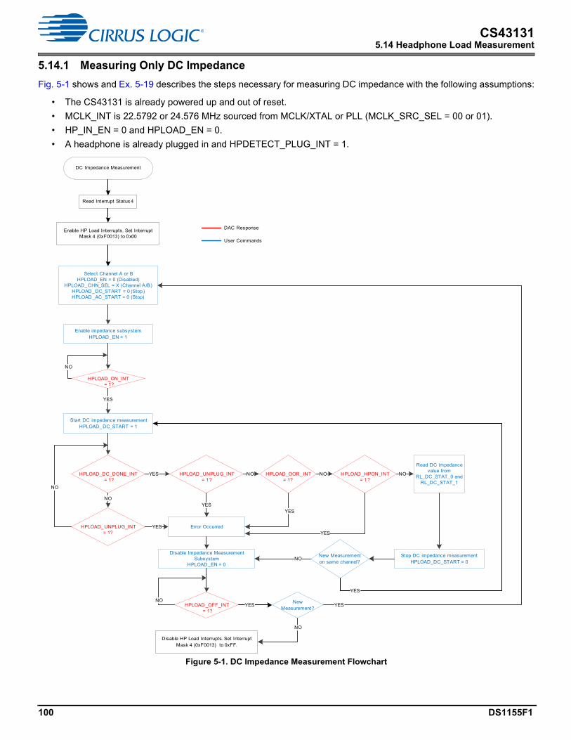
100 DS1155F1
CS431315.14 Headphone Load Measurement
5.14.1 Measuring Only DC Impedance
Fig. 5-1 shows and Ex. 5-19 describes the steps necessary for measuring DC impedance with the following assumptions:
• The CS43131 is already powered up and out of reset.
• MCLK_INT is 22.5792 or 24.576 MHz sourced from MCLK/XTAL or PLL (MCLK_SRC_SEL = 00 or 01).
• HP_IN_EN = 0 and HPLOAD_EN = 0.
• A headphone is already plugged in and HPDETECT_PLUG_INT = 1.
Figure 5-1. DC Impedance Measurement Flowchart
Start DC impedance measurementHPLOAD_DC_START = 1
HPLOAD_DC_DONE_INT= 1?
HPLOAD _UNPLUG_INT = 1?
HPLOAD_OOR_INT = 1?
Read DC impedance value from
RL_DC_STAT_0 and RL_DC_STAT_1
YES
Error Occurred
YES
NO
NO
YES
DAC Response
User Commands
DC Impedance Measurement
NO
New Measurement?
YES
HPLOAD_UNPLUG_INT = 1?
YES
NO
Enable HP Load Interrupts. Set Interrupt Mask 4 (0xF0013) to 0x00
Read Interrupt Status 4
Enable impedance subsystemHPLOAD _EN = 1
Disable Impedance Measurement Subsystem
HPLOAD _EN = 0
HPLOAD_ON_INT= 1?
YES
NO
HPLOAD _HPON_INT = 1?
NO
YES
Disable HP Load Interrupts. Set Interrupt Mask 4 (0xF0013) to 0xFF.
YESHPLOAD _OFF_INT= 1?
NO
NO
Select Channel A or BHPLOAD_EN = 0 (Disabled)
HPLOAD_CHN_SEL = X (Channel A/B)HPLOAD_DC_START = 0 (Stop)HPLOAD _AC_START = 0 (Stop)
YES
Stop DC impedance measurementHPLOAD_DC_START = 0
New Measurement on same channel?
NO

DS1155F1 101
CS431315.14 Headphone Load Measurement
Ex. 5-19 demonstrates measuring DC impedance for both channels of the CS43131.
Example 5-19. Sequence for DC Impedance Measurement
STEP TASK REGISTER/BIT FIELDS VALUE DESCRIPTION
1 Read Interrupt Status 4 register (0xF0003) to clear sticky bits.2 Enable HP Load Interrupts Interrupt Mask 4. 0xF0013 0x00
HPLOAD_NO_DC_INT_MASKHPLOAD_UNPLUG_INT_MASKHPLOAD_HPON_INT_MASKHPLOAD_OOR_INT_MASKHPLOAD_AC_DONE_INT_MASKHPLOAD_DC_DONE_INT_MASKHPLOAD_OFF_INT_MASKHPLOAD_ON_INT_MASK
00000000
Enable HPLOAD_NO_DC interruptEnable HPLOAD_UNPLUG interruptEnable HPLOAD_HPON interruptEnable HPLOAD_OOR interruptEnable HPLOAD_AC_DONE interruptEnable HPLOAD_DC_DONE interruptEnable HPLOAD_OFF interruptEnable HPLOAD_ON interrupt
3 Select Channel A HP Load 1. 0xE0000 0x00HPLOAD_ENReservedHPLOAD_CHN_SELReservedHPLOAD_AC_STARTHPLOAD_DC_START
00000000
HPOUTA selected
4 Enable impedance subsystem HP Load 1. 0xE0000 0x80HPLOAD_ENReservedHPLOAD_CHN_SELReservedHPLOAD_AC_STARTHPLOAD_DC_START
10000000
Enable impedance subsystem
5 Wait for interrupt. Check if HPLOAD_ON_INT = 1 in Interrupt Status 4 register (0xF0003)6 Start DC impedance measurement HP Load 1. 0xE0000 0x81
HPLOAD_ENReservedHPLOAD_CHN_SELReservedHPLOAD_AC_STARTHPLOAD_DC_START
10000001 Start DC impedance measurement
7 Wait for interrupt. Read Interrupt Status 4 register (0xF0003). If HPLOAD_UNPLUG_INT = 1, go to the last step as an error has occurred. If HPLOAD_OOR_INT = 1, go to the last step as an error has occurred. Otherwise, if HPLOAD_DC_DONE_INT = 1, go to the next step.
8 DC impedance values are available in HP DC Load Status 0 (0xE000D) and HP DC Load Status 1 (0xE000E) registers.9 Turn off impedance measurement
subsystemHP Load 1. 0xE0000 0x00
HPLOAD_ENReservedHPLOAD_CHN_SELReservedHPLOAD_AC_STARTHPLOAD_DC_START
00000000
Disable impedance measurement
Stop DC impedance measurement10 Wait for interrupt. Read Interrupt Status 4 register (0xF0003). Check for HPLOAD_OFF_INT = 1.11 Select Channel B HP Load 1. 0xE0000 0x10
HPLOAD_ENReservedHPLOAD_CHN_SELReservedHPLOAD_AC_STARTHPLOAD_DC_START
00010000
HPOUTB selected
12 Enable impedance subsystem HP Load 1. 0xE0000 0x90HPLOAD_ENReservedHPLOAD_CHN_SELReservedHPLOAD_AC_STARTHPLOAD_DC_START
10010000
Enable impedance subsystem
HPOUTB selected
13 Wait for interrupt. Check if HPLOAD_ON_INT = 1 in Interrupt Status 4 register (0xF0003)14 Start DC impedance measurement HP Load 1. 0xE0000 0x91
HPLOAD_ENReservedHPLOAD_CHN_SELReservedHPLOAD_AC_STARTHPLOAD_DC_START
10010001
HPOUTB selected
Start DC impedance measurement15 Wait for interrupt. Read Interrupt Status 4 register (0xF0003). If HPLOAD_UNPLUG_INT = 1, go to the last step as an error has occurred. If
HPLOAD_OOR_INT = 1, go to the last step as an error has occurred. Otherwise, if HPLOAD_DC_DONE_INT = 1, go to the next step.16 DC impedance values are available in HP DC Load Status 0 (0xE000D) and HP DC Load Status 1 (0xE000E) registers.

102 DS1155F1
CS431315.14 Headphone Load Measurement
17 Turn off impedance measurement subsystem
HP Load 1. 0xE0000 0x00HPLOAD_ENReservedHPLOAD_CHN_SELReservedHPLOAD_AC_STARTHPLOAD_DC_START
00000000
Disable impedance measurement subsystem
18 Wait for interrupt. Check if HPLOAD_OFF_INT = 1 in Interrupt Status 4 register (0xF0003).19 Disable HP Load Interrupts Interrupt Mask 4. 0xF0013 0xFF
Example 5-19. Sequence for DC Impedance Measurement (Cont.)
STEP TASK REGISTER/BIT FIELDS VALUE DESCRIPTION
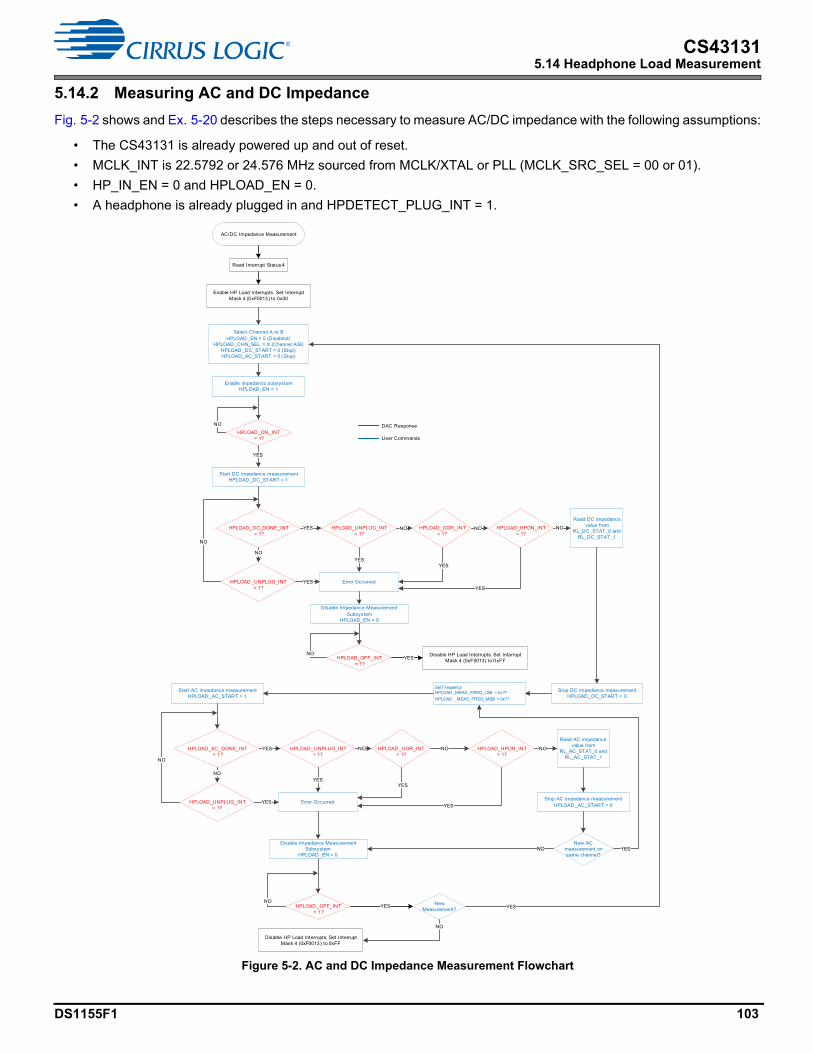
DS1155F1 103
CS431315.14 Headphone Load Measurement
5.14.2 Measuring AC and DC Impedance
Fig. 5-2 shows and Ex. 5-20 describes the steps necessary to measure AC/DC impedance with the following assumptions:
• The CS43131 is already powered up and out of reset.
• MCLK_INT is 22.5792 or 24.576 MHz sourced from MCLK/XTAL or PLL (MCLK_SRC_SEL = 00 or 01).
• HP_IN_EN = 0 and HPLOAD_EN = 0.
• A headphone is already plugged in and HPDETECT_PLUG_INT = 1.
Figure 5-2. AC and DC Impedance Measurement Flowchart
Select Channel A or BHPLOAD_EN = 0 (Disabled)
HPLOAD _CHN_SEL = X (Channel A/B)HPLOAD _DC_START = 0 (Stop)HPLOAD_AC_START = 0 (Stop)
Start DC impedance measurementHPLOAD _DC_START = 1
HPLOAD_DC_DONE_INT= 1?
HPLOAD_UNPLUG_INT = 1?
HPLOAD_OOR _INT = 1?
Read DC impedance value from
RL_DC_STAT_0 and RL_DC_STAT_1
YES
Error Occurred
YES
NO
NO
YES
DAC Response
User Commands
AC/DC Impedance Measurement
NO
HPLOAD _UNPLUG_INT = 1?
YES
NO
Enable HP Load Interrupts. Set Interrupt Mask 4 (0xF0013) to 0x00
Read Interrupt Status 4
Enable impedance subsystemHPLOAD_EN = 1
Disable Impedance Measurement Subsystem
HPLOAD_EN = 0
HPLOAD_ON_INT= 1?
YES
NO
HPLOAD_HPON_INT = 1?
NO
YES
YESHPLOAD_OFF_INT= 1?
NO
Start AC impedance measurementHPLOAD _AC_START = 1
HPLOAD_AC_DONE_INT= 1?
HPLOAD_UNPLUG_INT = 1?
HPLOAD _OOR_INT = 1?
Read AC impedance value from
RL_AC_STAT_0 and RL_AC_STAT_1
YES
Error Occurred
YES
NO
NO
YES
NO
HPLOAD_UNPLUG_INT = 1?
YES
NO
Disable Impedance Measurement Subsystem
HPLOAD _EN = 0
HPLOAD_HPON_INT = 1?
NO
YES
YESHPLOAD_OFF_INT= 1?
NO
Disable HP Load Interrupts. Set Interrupt Mask 4 (0xF0013) to 0xFF
New Measurement?
Disable HP Load Interrupts. Set Interrupt Mask 4 (0xF0013) to 0xFF
NO
YES
Set FrequencyHPLOAD _MEAS_FREQ_LSB = 0x??
HPLOAD _MEAS_FREQ_MSB = 0x??
New AC measurement on same channel?
NO YES
Stop DC impedance measurementHPLOAD_DC_START = 0
Stop AC impedance measurementHPLOAD _AC_START = 0

104 DS1155F1
CS431315.14 Headphone Load Measurement
Ex. 5-20 demonstrates measuring both AC and DC impedance for both channels of the CS43131.
Example 5-20. AC and DC Impedance Measurement
STEP TASK REGISTER/BIT FIELDS VALUE DESCRIPTION
1 Read Interrupt Status 4 register (0xF0003) to clear sticky bits.2 Enable HP Load Interrupts Interrupt Mask 4. 0xF0013 0x00
HPLOAD_NO_DC_INT_MASKHPLOAD_UNPLUG_INT_MASKHPLOAD_HPON_INT_MASKHPLOAD_OOR_INT_MASKHPLOAD_AC_DONE_INT_MASKHPLOAD_DC_DONE_INT_MASKHPLOAD_OFF_INT_MASKHPLOAD_ON_INT_MASK
00000000
Enable HPLOAD_NO_DC interruptEnable HPLOAD_UNPLUG interruptEnable HPLOAD_HPON interruptEnable HPLOAD_OOR interruptEnable HPLOAD_AC_DONE interruptEnable HPLOAD_DC_DONE interruptEnable HPLOAD_OFF interruptEnable HPLOAD_ON interrupt
3 Select Channel A HP Load 1. 0xE0000 0x00HPLOAD_ENReservedHPLOAD_CHN_SELReservedHPLOAD_AC_STARTHPLOAD_DC_START
00000000
HPOUTA selected
4 Enable impedance subsystem HP Load 1. 0xE0000 0x80HPLOAD_ENReservedHPLOAD_CHN_SELReservedHPLOAD_AC_STARTHPLOAD_DC_START
10000000
Enable impedance subsystem
5 Wait for interrupt. Check if HPLOAD_ON_INT = 1 in Interrupt Status 4 register (0xF0003)6 Start DC impedance measurement HP Load 1. 0xE0000 0x81
HPLOAD_ENReservedHPLOAD_CHN_SELReservedHPLOAD_AC_STARTHPLOAD_DC_START
10000001 Start DC impedance measurement
7 Wait for interrupt. Read Interrupt Status 4 register (0xF0003). If HPLOAD_UNPLUG_INT = 1, go to the last step as an error has occurred. If HPLOAD_OOR_INT = 1, go to the last step as an error has occurred. Otherwise, if HPLOAD_DC_DONE_INT = 1, go to the next step.
8 DC impedance values are available in HP DC Load Status 0 (0xE000D) and HP DC Load Status 1 (0xE000E) registers.9 Set HP load measurement frequency to
desired frequency. Assuming 1 kHz.HP Load Measurement 1. 0xE0003 0xA8
HPLOAD_MEAS_FREQ_LSB 0xA8 Set measurement frequency = 1 kHzHP Load Measurement 2. 0xE0004 0x00
HPLOAD_MEAS_FREQ_MSB 0x00 MSB of load measurement frequency10 Start AC impedance measurement HP Load 1. 0xE0000 0x82
HPLOAD_ENReservedHPLOAD_CHN_SELReservedHPLOAD_AC_STARTHPLOAD_DC_START
10000010
Start AC impedance measurement
11 Wait for interrupt. Read Interrupt Status 4 register (0xF0003). If HPLOAD_UNPLUG_INT = 1, go to the last step as an error has occurred. If HPLOAD_OOR_INT = 1, go to the last step as an error has occurred. Otherwise, if HPLOAD_AC_DONE_INT = 1, go to the next step.
12 AC impedance values are available in HP AC Load Status 0 (0xE0010) and HP AC Load Status 1 (0xE0011) registers.13 Stop AC impedance measurement. HP Load 1. 0xE0000 0x8014 If another frequency point is desired, go back to step 9. Otherwise continue.15 Disable impedance measurement
subsystem and select channel BHP Load 1. 0xE0000 0x10
16 Wait for interrupt. Read Interrupt Status 4 register (0xF0003). Check for HPLOAD_OFF_INT = 1. If Channel B measurement is desired, continue to the next step; otherwise go to step 30 to end the impedance measurement.
17 Enable impedance subsystem HP Load 1. 0xE0000 0x90HPLOAD_ENReservedHPLOAD_CHN_SELReservedHPLOAD_AC_STARTHPLOAD_DC_START
10010000
Enable impedance subsystem
HPOUTB selected
18 Wait for interrupt. Check if HPLOAD_ON_INT = 1 in Interrupt Status 4 register (0xF0003)
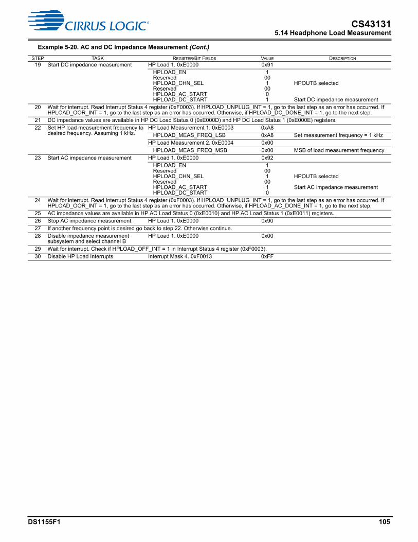
DS1155F1 105
CS431315.14 Headphone Load Measurement
19 Start DC impedance measurement HP Load 1. 0xE0000 0x91HPLOAD_ENReservedHPLOAD_CHN_SELReservedHPLOAD_AC_STARTHPLOAD_DC_START
10010001
HPOUTB selected
Start DC impedance measurement20 Wait for interrupt. Read Interrupt Status 4 register (0xF0003). If HPLOAD_UNPLUG_INT = 1, go to the last step as an error has occurred. If
HPLOAD_OOR_INT = 1, go to the last step as an error has occurred. Otherwise, if HPLOAD_DC_DONE_INT = 1, go to the next step.21 DC impedance values are available in HP DC Load Status 0 (0xE000D) and HP DC Load Status 1 (0xE000E) registers.22 Set HP load measurement frequency to
desired frequency. Assuming 1 kHz.HP Load Measurement 1. 0xE0003 0xA8
HPLOAD_MEAS_FREQ_LSB 0xA8 Set measurement frequency = 1 kHzHP Load Measurement 2. 0xE0004 0x00
HPLOAD_MEAS_FREQ_MSB 0x00 MSB of load measurement frequency23 Start AC impedance measurement HP Load 1. 0xE0000 0x92
HPLOAD_ENReservedHPLOAD_CHN_SELReservedHPLOAD_AC_STARTHPLOAD_DC_START
10010010
HPOUTB selected
Start AC impedance measurement
24 Wait for interrupt. Read Interrupt Status 4 register (0xF0003). If HPLOAD_UNPLUG_INT = 1, go to the last step as an error has occurred. If HPLOAD_OOR_INT = 1, go to the last step as an error has occurred. Otherwise, if HPLOAD_AC_DONE_INT = 1, go to the next step.
25 AC impedance values are available in HP AC Load Status 0 (0xE0010) and HP AC Load Status 1 (0xE0011) registers.26 Stop AC impedance measurement. HP Load 1. 0xE0000 0x9027 If another frequency point is desired go back to step 22. Otherwise continue.28 Disable impedance measurement
subsystem and select channel BHP Load 1. 0xE0000 0x00
29 Wait for interrupt. Check if HPLOAD_OFF_INT = 1 in Interrupt Status 4 register (0xF0003).30 Disable HP Load Interrupts Interrupt Mask 4. 0xF0013 0xFF
Example 5-20. AC and DC Impedance Measurement (Cont.)
STEP TASK REGISTER/BIT FIELDS VALUE DESCRIPTION
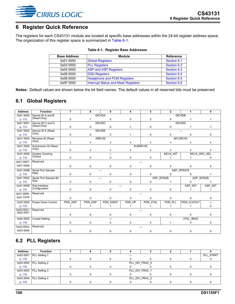
106 DS1155F1
CS431316 Register Quick Reference
6 Register Quick Reference
The registers for each CS43131 module are located at specific base addresses within the 24-bit register address space. The organization of this register space is summarized in Table 6-1.
Notes: Default values are shown below the bit field names. The default values in all reserved bits must be preserved.
6.1 Global Registers
6.2 PLL Registers
Table 6-1. Register Base Addresses
Base Address Module Reference0x01 0000 Global Registers Section 6.10x03 0000 PLL Registers Section 6.20x04 0000 ASP and XSP Registers Section 6.30x06 0000 DSD Registers Section 6.40x08 0000 Headphone and PCM Registers Section 6.50x0F 0000 Interrupt Status and Mask Registers Section 6.6
Address Function 7 6 5 4 3 2 1 0
0x01 0000 Device ID A and B (Read Only)
DEVIDA DEVIDB
p. 113 0 1 0 0 0 0 1 1
0x01 0001 Device ID C and D (Read Only)
DEVIDC DEVIDD
p. 113 0 0 0 1 0 0 1 1
0x01 0002 Device ID E (Read Only)
DEVIDE —
p. 113 0 0 0 1 0 0 0 0
0x01 0004 Revision ID (Read Only)
AREVID MTLREVID
p. 113 x x x x x x x x
0x01 0005 Subrevision ID (Read Only)
SUBREVID
p. 113 0 x x x x x x x
0x01 0006 System Clocking Control
— MCLK_INT MCLK_SRC_SEL
p. 114 0 0 0 0 0 1 1 0
0x01 0007–0x01 000A
Reserved —
0 0 0 0 0 0 0 0
0x01 000B Serial Port Sample Rate
— ASP_SPRATE
p. 114 0 0 0 0 0 0 0 1
0x01 000C Serial Port Sample Bit Size
— XSP_SPSIZE ASP_SPSIZE
p. 114 0 0 0 0 0 1 0 1
0x01 000D Pad Interface Configuration
— XSP_3ST ASP_3ST
p. 114 0 0 0 0 0 0 1 1
0x01 000E–0x01 FFFF
Reserved —
0 0 0 0 0 0 0 0
0x02 0000 Power Down Control PDN_XSP PDN_ASP PDN_DSDIF PDN_HP PDN_XTAL PDN_PLL PDN_CLKOUT —
p. 115 1 1 1 1 1 1 1 0
0x02 0001–0x02 0051
Reserved —
0 0 0 0 0 0 0 0
0x02 0052 Crystal Setting — XTAL_IBIAS
p. 115 0 0 0 0 0 1 0 0
0x02 0053–0x03 0000
Reserved —
0 0 0 0 0 0 0 0
Address Function 7 6 5 4 3 2 1 0
0x03 0001 PLL Setting 1 — PLL_START
p. 116 0 0 0 0 0 0 0 0
0x03 0002 PLL Setting 2 PLL_DIV_FRAC_0
p. 116 0 0 0 0 0 0 0 0
0x03 0003 PLL Setting 3 PLL_DIV_FRAC_1
p. 116 0 0 0 0 0 0 0 0
0x03 0004 PLL Setting 4 PLL_DIV_FRAC_2
p. 116 0 0 0 0 0 0 0 0
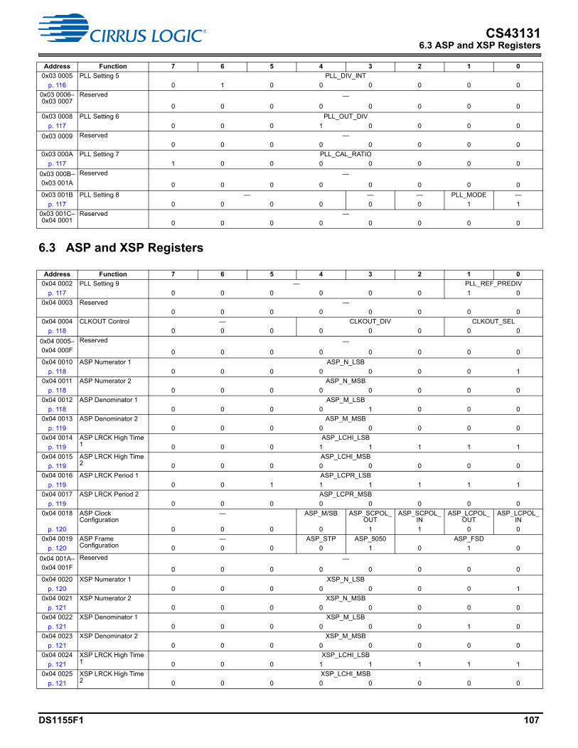
DS1155F1 107
CS431316.3 ASP and XSP Registers
6.3 ASP and XSP Registers
0x03 0005 PLL Setting 5 PLL_DIV_INT
p. 116 0 1 0 0 0 0 0 0
0x03 0006–0x03 0007
Reserved —
0 0 0 0 0 0 0 0
0x03 0008 PLL Setting 6 PLL_OUT_DIV
p. 117 0 0 0 1 0 0 0 0
0x03 0009 Reserved —
0 0 0 0 0 0 0 0
0x03 000A PLL Setting 7 PLL_CAL_RATIO
p. 117 1 0 0 0 0 0 0 0
0x03 000B–0x03 001A
Reserved —
0 0 0 0 0 0 0 0
0x03 001B PLL Setting 8 — — — PLL_MODE —
p. 117 0 0 0 0 0 0 1 1
0x03 001C–0x04 0001
Reserved —
0 0 0 0 0 0 0 0
Address Function 7 6 5 4 3 2 1 0
0x04 0002 PLL Setting 9 — PLL_REF_PREDIV
p. 117 0 0 0 0 0 0 1 0
0x04 0003 Reserved —
0 0 0 0 0 0 0 0
0x04 0004 CLKOUT Control — CLKOUT_DIV CLKOUT_SEL
p. 118 0 0 0 0 0 0 0 0
0x04 0005–0x04 000F
Reserved —
0 0 0 0 0 0 0 0
0x04 0010 ASP Numerator 1 ASP_N_LSB
p. 118 0 0 0 0 0 0 0 1
0x04 0011 ASP Numerator 2 ASP_N_MSB
p. 118 0 0 0 0 0 0 0 0
0x04 0012 ASP Denominator 1 ASP_M_LSB
p. 118 0 0 0 0 1 0 0 0
0x04 0013 ASP Denominator 2 ASP_M_MSB
p. 119 0 0 0 0 0 0 0 0
0x04 0014 ASP LRCK High Time 1
ASP_LCHI_LSB
p. 119 0 0 0 1 1 1 1 1
0x04 0015 ASP LRCK High Time 2
ASP_LCHI_MSB
p. 119 0 0 0 0 0 0 0 0
0x04 0016 ASP LRCK Period 1 ASP_LCPR_LSB
p. 119 0 0 1 1 1 1 1 1
0x04 0017 ASP LRCK Period 2 ASP_LCPR_MSB
p. 119 0 0 0 0 0 0 0 0
0x04 0018 ASP Clock Configuration
— ASP_M/SB ASP_SCPOL_OUT
ASP_SCPOL_IN
ASP_LCPOL_OUT
ASP_LCPOL_IN
p. 120 0 0 0 0 1 1 0 0
0x04 0019 ASP Frame Configuration
— ASP_STP ASP_5050 ASP_FSD
p. 120 0 0 0 0 1 0 1 0
0x04 001A–0x04 001F
Reserved —
0 0 0 0 0 0 0 0
0x04 0020 XSP Numerator 1 XSP_N_LSB
p. 120 0 0 0 0 0 0 0 1
0x04 0021 XSP Numerator 2 XSP_N_MSB
p. 121 0 0 0 0 0 0 0 0
0x04 0022 XSP Denominator 1 XSP_M_LSB
p. 121 0 0 0 0 0 0 1 0
0x04 0023 XSP Denominator 2 XSP_M_MSB
p. 121 0 0 0 0 0 0 0 0
0x04 0024 XSP LRCK High Time 1
XSP_LCHI_LSB
p. 121 0 0 0 1 1 1 1 1
0x04 0025 XSP LRCK High Time 2
XSP_LCHI_MSB
p. 121 0 0 0 0 0 0 0 0
Address Function 7 6 5 4 3 2 1 0
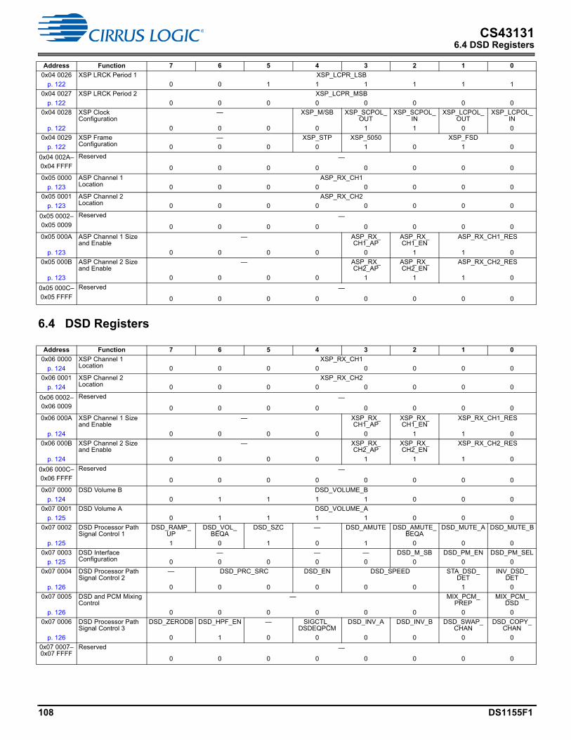
108 DS1155F1
CS431316.4 DSD Registers
6.4 DSD Registers
0x04 0026 XSP LRCK Period 1 XSP_LCPR_LSB
p. 122 0 0 1 1 1 1 1 1
0x04 0027 XSP LRCK Period 2 XSP_LCPR_MSB
p. 122 0 0 0 0 0 0 0 0
0x04 0028 XSP Clock Configuration
— XSP_M/SB XSP_SCPOL_OUT
XSP_SCPOL_IN
XSP_LCPOL_OUT
XSP_LCPOL_IN
p. 122 0 0 0 0 1 1 0 0
0x04 0029 XSP Frame Configuration
— XSP_STP XSP_5050 XSP_FSD
p. 122 0 0 0 0 1 0 1 0
0x04 002A–0x04 FFFF
Reserved —
0 0 0 0 0 0 0 0
0x05 0000 ASP Channel 1 Location
ASP_RX_CH1
p. 123 0 0 0 0 0 0 0 0
0x05 0001 ASP Channel 2 Location
ASP_RX_CH2
p. 123 0 0 0 0 0 0 0 0
0x05 0002–0x05 0009
Reserved —
0 0 0 0 0 0 0 0
0x05 000A ASP Channel 1 Size and Enable
— ASP_RX_CH1_AP
ASP_RX_CH1_EN
ASP_RX_CH1_RES
p. 123 0 0 0 0 0 1 1 0
0x05 000B ASP Channel 2 Size and Enable
— ASP_RX_CH2_AP
ASP_RX_CH2_EN
ASP_RX_CH2_RES
p. 123 0 0 0 0 1 1 1 0
0x05 000C–0x05 FFFF
Reserved —
0 0 0 0 0 0 0 0
Address Function 7 6 5 4 3 2 1 0
0x06 0000 XSP Channel 1 Location
XSP_RX_CH1
p. 124 0 0 0 0 0 0 0 0
0x06 0001 XSP Channel 2 Location
XSP_RX_CH2
p. 124 0 0 0 0 0 0 0 0
0x06 0002–0x06 0009
Reserved —
0 0 0 0 0 0 0 0
0x06 000A XSP Channel 1 Size and Enable
— XSP_RX_CH1_AP
XSP_RX_CH1_EN
XSP_RX_CH1_RES
p. 124 0 0 0 0 0 1 1 0
0x06 000B XSP Channel 2 Size and Enable
— XSP_RX_CH2_AP
XSP_RX_CH2_EN
XSP_RX_CH2_RES
p. 124 0 0 0 0 1 1 1 0
0x06 000C–0x06 FFFF
Reserved —
0 0 0 0 0 0 0 0
0x07 0000 DSD Volume B DSD_VOLUME_B
p. 124 0 1 1 1 1 0 0 0
0x07 0001 DSD Volume A DSD_VOLUME_A
p. 125 0 1 1 1 1 0 0 0
0x07 0002 DSD Processor Path Signal Control 1
DSD_RAMP_UP
DSD_VOL_BEQA
DSD_SZC — DSD_AMUTE DSD_AMUTE_BEQA
DSD_MUTE_A DSD_MUTE_B
p. 125 1 0 1 0 1 0 0 0
0x07 0003 DSD Interface Configuration
— — — DSD_M_SB DSD_PM_EN DSD_PM_SEL
p. 125 0 0 0 0 0 0 0 0
0x07 0004 DSD Processor Path Signal Control 2
— DSD_PRC_SRC DSD_EN DSD_SPEED STA_DSD_DET
INV_DSD_DET
p. 126 0 0 0 0 0 0 1 0
0x07 0005 DSD and PCM Mixing Control
— MIX_PCM_PREP
MIX_PCM_DSD
p. 126 0 0 0 0 0 0 0 0
0x07 0006 DSD Processor Path Signal Control 3
DSD_ZERODB DSD_HPF_EN — SIGCTL_DSDEQPCM
DSD_INV_A DSD_INV_B DSD_SWAP_CHAN
DSD_COPY_CHAN
p. 126 0 1 0 0 0 0 0 0
0x07 0007–0x07 FFFF
Reserved —
0 0 0 0 0 0 0 0
Address Function 7 6 5 4 3 2 1 0
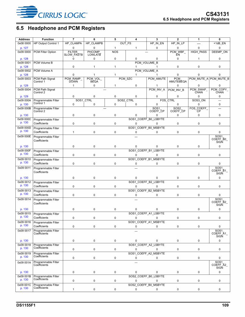
DS1155F1 109
CS431316.5 Headphone and PCM Registers
6.5 Headphone and PCM Registers
Address Function 7 6 5 4 3 2 1 0
0x08 0000 HP Output Control 1 HP_CLAMPA HP_CLAMPB OUT_FS HP_IN_EN HP_IN_LP — +1dB_EN
p. 127 0 0 1 1 0 0 0 0
0x09 0000 PCM Filter Option FILTER_SLOW_FASTB
PHCOMP_LOWLATB
NOS — PCM_WBF_EN
HIGH_PASS DEEMP_ON
p. 128 0 0 0 0 0 0 1 0
0x09 0001 PCM Volume B PCM_VOLUME_B
p. 128 0 1 1 1 1 0 0 0
0x09 0002 PCM Volume A PCM_VOLUME_A
p. 128 0 1 1 1 1 0 0 0
0x09 0003 PCM Path Signal Control 1
PCM_RAMP_DOWN
PCM_VOL_BEQA
PCM_SZC PCM_AMUTE PCM_AMUTEBEQA
PCM_MUTE_A PCM_MUTE_B
p. 129 1 0 1 0 1 0 0 0
0x09 0004 PCM Path Signal Control 2
— PCM_INV_A PCM_INV_B PCM_SWAP_CHAN
PCM_COPY_CHAN
p. 129 0 0 0 0 0 0 0 0
0x09 000A Programmable Filter Control 1
SOS1_CTRL SOS2_CTRL FOS_CTRL SOS3_ON —
p. 130 0 0 0 0 0 0 0 0
0x09 000B Programmable Filter Control 2
— SOS1_COEFF_CP
SOS2_COEFF_CP
FOS_COEFF_CP
—
p. 130 0 0 0 0 0 0 0 0
0x09 000Cp. 130
Programmable Filter Coefficients
SOS1_COEFF_B0_LSBYTE
0 0 0 0 0 0 0 0
0x09 000Dp. 130
Programmable Filter Coefficients
SOS1_COEFF_B0_MSBYTE
1 0 0 0 0 0 0 0
0x09 000E Programmable Filter Coefficients
— SOS1_COEFF_B0_
SIGN
p. 130 0 0 0 0 0 0 0 0
0x09 000Fp. 130
Programmable Filter Coefficients
SOS1_COEFF_B1_LSBYTE
0 0 0 0 0 0 0 0
0x09 0010p. 130
Programmable Filter Coefficients
SOS1_COEFF_B1_MSBYTE
0 0 0 0 0 0 0 0
0x09 0011 Programmable Filter Coefficients
— SOS1_COEFF_B1_
SIGN
p. 130 0 0 0 0 0 0 0 0
0x09 0012p. 130
Programmable Filter Coefficients
SOS1_COEFF_B2_LSBYTE
0 0 0 0 0 0 0 0
0x09 0013p. 130
Programmable Filter Coefficients
SOS1_COEFF_B2_MSBYTE
0 0 0 0 0 0 0 0
0x09 0014 Programmable Filter Coefficients
— SOS1_COEFF_B2_
SIGN
p. 130 0 0 0 0 0 0 0 0
0x09 0015p. 130
Programmable Filter Coefficients
SOS1_COEFF_A1_LSBYTE
0 0 0 0 0 0 0 0
0x09 0016p. 130
Programmable Filter Coefficients
SOS1_COEFF_A1_MSBYTE
0 0 0 0 0 0 0 0
0x09 0017 Programmable Filter Coefficients
— SOS1_COEFF_A1_
SIGN
p. 130 0 0 0 0 0 0 0 0
0x09 0018p. 130
Programmable Filter Coefficients
SOS1_COEFF_A2_LSBYTE
0 0 0 0 0 0 0 0
0x09 0019p. 130
Programmable Filter Coefficients
SOS1_COEFF_A2_MSBYTE
0 0 0 0 0 0 0 0
0x09 001A Programmable Filter Coefficients
— SOS1_COEFF_A2_
SIGN
p. 130 0 0 0 0 0 0 0 0
0x09 001Bp. 130
Programmable Filter Coefficients
SOS2_COEFF_B0_LSBYTE
0 0 0 0 0 0 0 0
0x09 001Cp. 130
Programmable Filter Coefficients
SOS2_COEFF_B0_MSBYTE
1 0 0 0 0 0 0 0

110 DS1155F1
CS431316.5 Headphone and PCM Registers
0x09 001D Programmable Filter Coefficients
— SOS2_COEFF_B0_
SIGN
p. 130 0 0 0 0 0 0 0 0
0x09 001Ep. 130
Programmable Filter Coefficients
SOS2_COEFF_B1_LSBYTE
0 0 0 0 0 0 0 0
0x09 001Fp. 130
Programmable Filter Coefficients
SOS2_COEFF_B1_MSBYTE
0 0 0 0 0 0 0 0
0x09 0020 Programmable Filter Coefficients
— SOS2_COEFF_B1_
SIGN
p. 130 0 0 0 0 0 0 0 0
0x09 0021p. 130
Programmable Filter Coefficients
SOS2_COEFF_B2_LSBYTE
0 0 0 0 0 0 0 0
0x09 0022p. 130
Programmable Filter Coefficients
SOS2_COEFF_B2_MSBYTE
0 0 0 0 0 0 0 0
0x09 0023 Programmable Filter Coefficients
— SOS2_COEFF_B2_
SIGN
p. 130 0 0 0 0 0 0 0 0
0x09 0024p. 130
Programmable Filter Coefficients
SOS2_COEFF_A1_LSBYTE
0 0 0 0 0 0 0 0
0x09 0025p. 130
Programmable Filter Coefficients
SOS2_COEFF_A1_MSBYTE
0 0 0 0 0 0 0 0
0x09 0026 Programmable Filter Coefficients
— SOS2_COEFF_A1_
SIGN
p. 130 0 0 0 0 0 0 0 0
0x09 0027p. 130
Programmable Filter Coefficients
SOS2_COEFF_A2_LSBYTE
0 0 0 0 0 0 0 0
0x09 0028p. 130
Programmable Filter Coefficients
SOS2_COEFF_A2_MSBYTE
0 0 0 0 0 0 0 0
0x09 0029 Programmable Filter Coefficients
— SOS2_COEFF_A2_
SIGN
p. 130 0 0 0 0 0 0 0 0
0x09 002Ap. 130
Programmable Filter Coefficients
SOS3_COEFF_B0_LSBYTE
0 0 0 0 0 0 0 0
0x09 002Bp. 130
Programmable Filter Coefficients
SOS3_COEFF_B0_MSBYTE
1 0 0 0 0 0 0 0
0x09 002C Programmable Filter Coefficients
— SOS3_COEFF_B0_
SIGN
p. 130 0 0 0 0 0 0 0 0
0x09 002Dp. 130
Programmable Filter Coefficients
SOS3_COEFF_B1_LSBYTE
0 0 0 0 0 0 0 0
0x09 002Ep. 130
Programmable Filter Coefficients
SOS3_COEFF_B1_MSBYTE
0 0 0 0 0 0 0 0
0x09 002F Programmable Filter Coefficients
— SOS3_COEFF_B1_
SIGN
p. 130 0 0 0 0 0 0 0 0
0x09 0030p. 130
Programmable Filter Coefficients
SOS3_COEFF_B2_LSBYTE
0 0 0 0 0 0 0 0
0x09 0031p. 130
Programmable Filter Coefficients
SOS3_COEFF_B2_MSBYTE
0 0 0 0 0 0 0 0
0x09 0032 Programmable Filter Coefficients
— SOS3_COEFF_B2_
SIGN
p. 130 0 0 0 0 0 0 0 0
0x09 0033p. 130
Programmable Filter Coefficients
SOS3_COEFF_A1_LSBYTE
0 0 0 0 0 0 0 0
0x09 0034p. 130
Programmable Filter Coefficients
SOS3_COEFF_A1_MSBYTE
0 0 0 0 0 0 0 0
0x09 0035 Programmable Filter Coefficients
— SOS3_COEFF_A1_
SIGN
p. 130 0 0 0 0 0 0 0 0
Address Function 7 6 5 4 3 2 1 0

DS1155F1 111
CS431316.5 Headphone and PCM Registers
0x09 0036p. 130
Programmable Filter Coefficients
SOS3_COEFF_A2_LSBYTE
0 0 0 0 0 0 0 0
0x09 0037p. 130
Programmable Filter Coefficients
SOS3_COEFF_A2_MSBYTE
0 0 0 0 0 0 0 0
0x09 0038 Programmable Filter Coefficients
— SOS3_COEFF_A2_
SIGN
p. 130 0 0 0 0 0 0 0 0
0x09 0039p. 130
Programmable Filter Coefficients
FOS_COEFF_B0_LSBYTE
0 0 0 0 0 0 0 0
0x09 003Ap. 130
Programmable Filter Coefficients
FOS_COEFF_B0_MSBYTE
1 0 0 0 0 0 0 0
0x09 003B Programmable Filter Coefficients
— FOS_COEFF_B0_SIGN
p. 130 0 0 0 0 0 0 0 0
0x09 003Cp. 130
Programmable Filter Coefficients
FOS_COEFF_B1_LSBYTE
0 0 0 0 0 0 0 0
0x09 003Dp. 130
Programmable Filter Coefficients
FOS_COEFF_B1_MSBYTE
0 0 0 0 0 0 0 0
0x09 003E Programmable Filter Coefficients
— FOS_COEFF_B1_SIGN
p. 130 0 0 0 0 0 0 0 0
0x09 003Fp. 130
Programmable Filter Coefficients
FOS_COEFF_A1_LSBYTE
0 0 0 0 0 0 0 0
0x09 0040p. 130
Programmable Filter Coefficients
FOS_COEFF_A1_MSBYTE
0 0 0 0 0 0 0 0
0x09 0041 Programmable Filter Coefficients
— FOS_COEFF_A1_SIGN
p. 130 0 0 0 0 0 0 0 0
0x0B 0000 Class H Control — ADPT_PWR HV_EN EXT_VCPFILT
p. 131 0 0 0 1 1 1 1 0
0x0D 0000 HP Detect HPDETECT_CTRL HPDETECT_INV
HPDETECT_RISE_DBC_TIME HPDETECT_FALL_DBC_TIME —
p. 131 0 0 0 0 0 1 0 0
0x0D 0001 HP Status (Read Only) — HPDETECT_PLUG_DBC
HPDETECT_UNPLUG_DBC
—
p. 131 0 0 0 0 0 0 0 0
0x0D 0002–0x0D FFFF
Reserved —
0 0 0 0 0 0 0 0
0x0E 0000 HP Load 1 HPLOAD_EN — HPLOAD_CHN_SEL
— HPLOAD_AC_START
HPLOAD_DC_START
p. 132 0 0 0 0 0 0 0 0
0x0E 0001–0x0E 0002
Reserved —
0 0 0 0 0 0 0 0
0x0E 0003 HP Load Measurement 1
HPLOAD_MEAS_FREQ_LSB
p. 132 0 0 0 0 0 0 0 0
0x0E 0004 HP Load Measurement 2
HPLOAD_MEAS_FREQ_MSB
p. 132 0 0 0 0 0 0 0 0
0x0E 0005–0x0E 000C
Reserved —
0 0 0 0 0 0 0 0
0x0E 000D HP DC Load Status 0 (Read Only)
RL_DC_STAT_0
p. 133 0 0 0 0 0 0 0 0
0x0E 000E HP DC Load Status 1 (Read Only)
RL_DC_STAT_1
p. 133 0 0 0 0 0 0 0 0
0x0E 000F Reserved —
0 0 0 0 0 0 0 0
0x0E 0010 HP AC Load Status 0 (Read Only)
RL_AC_STAT_0
p. 133 0 0 0 0 0 0 0 0
0x0E 0011 HP AC Load Status 1 (Read Only)
RL_AC_STAT_1
p. 133 0 0 0 0 0 0 0 0
0x0E 0012–0x0E 0019
Reserved —
0 0 0 0 0 0 0 0
Address Function 7 6 5 4 3 2 1 0
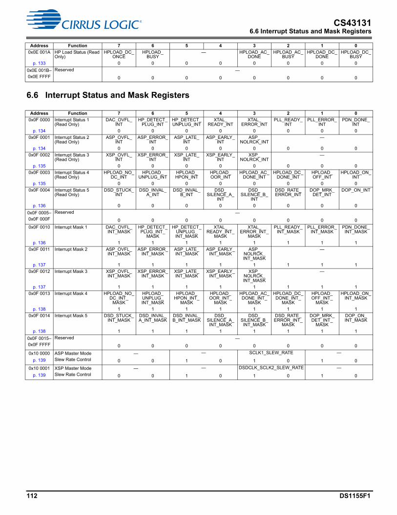
112 DS1155F1
CS431316.6 Interrupt Status and Mask Registers
6.6 Interrupt Status and Mask Registers
0x0E 001A HP Load Status (Read Only)
HPLOAD_DC_ONCE
HPLOAD_BUSY
— HPLOAD_AC_DONE
HPLOAD_AC_BUSY
HPLOAD_DC_DONE
HPLOAD_DC_BUSY
p. 133 0 0 0 0 0 0 0 0
0x0E 001B–0x0E FFFF
Reserved —
0 0 0 0 0 0 0 0
Address Function 7 6 5 4 3 2 1 0
0x0F 0000 Interrupt Status 1 (Read Only)
DAC_OVFL_INT
HP_DETECT_PLUG_INT
HP_DETECT_UNPLUG_INT
XTAL_READY_INT
XTAL_ERROR_INT
PLL_READY_INT
PLL_ERROR_INT
PDN_DONE_INT
p. 134 0 0 0 0 0 0 0 0
0x0F 0001 Interrupt Status 2 (Read Only)
ASP_OVFL_INT
ASP_ERROR_INT
ASP_LATE_INT
ASP_EARLY_INT
ASP_NOLRCK_INT
—
p. 134 0 0 0 0 0 0 0 0
0x0F 0002 Interrupt Status 3 (Read Only)
XSP_OVFL_INT
XSP_ERROR_INT
XSP_LATE_INT
XSP_EARLY_INT
XSP_NOLRCK_INT
—
p. 135 0 0 0 0 0 0 0 0
0x0F 0003 Interrupt Status 4 (Read Only)
HPLOAD_NO_DC_INT
HPLOAD_UNPLUG_INT
HPLOAD_HPON_INT
HPLOAD_OOR_INT
HPLOAD_AC_DONE_INT
HPLOAD_DC_DONE_INT
HPLOAD_OFF_INT
HPLOAD_ON_INT
p. 135 0 0 0 0 0 0 0 0
0x0F 0004 Interrupt Status 5 (Read Only)
DSD_STUCK_INT
DSD_INVAL_A_INT
DSD_INVAL_B_INT
DSD_SILENCE_A_
INT
DSD_SILENCE_B_
INT
DSD_RATE_ERROR_INT
DOP_MRK_DET_INT
DOP_ON_INT
p. 136 0 0 0 0 0 0 0 0
0x0F 0005–0x0F 000F
Reserved —
0 0 0 0 0 0 0 0
0x0F 0010 Interrupt Mask 1 DAC_OVFL_INT_MASK
HP_DETECT_PLUG_INT_
MASK
HP_DETECT_UNPLUG_INT_MASK
XTAL_READY_INT_
MASK
XTAL_ERROR_INT_
MASK
PLL_READY_INT_MASK
PLL_ERROR_INT_MASK
PDN_DONE_INT_MASK
p. 136 1 1 1 1 1 1 1 1
0x0F 0011 Interrupt Mask 2 ASP_OVFL_INT_MASK
ASP_ERROR_INT_MASK
ASP_LATE_INT_MASK
ASP_EARLY_INT_MASK
ASP_NOLRCK_INT_MASK
—
p. 137 1 1 1 1 1 1 1 1
0x0F 0012 Interrupt Mask 3 XSP_OVFL_INT_MASK
XSP_ERROR_INT_MASK
XSP_LATE_INT_MASK
XSP_EARLY_INT_MASK
XSP_NOLRCK_INT_MASK
—
p. 137 1 1 1 1 1 1 1 1
0x0F 0013 Interrupt Mask 4 HPLOAD_NO_DC_INT_
MASK
HPLOAD_UNPLUG_INT_MASK
HPLOAD_HPON_INT_
MASK
HPLOAD_OOR_INT_
MASK
HPLOAD_AC_DONE_INT_
MASK
HPLOAD_DC_DONE_INT_
MASK
HPLOAD_OFF_INT_
MASK
HPLOAD_ON_INT_MASK
p. 138 1 1 1 1 1 1 1 1
0x0F 0014 Interrupt Mask 5 DSD_STUCK_INT_MASK
DSD_INVAL_A_INT_MASK
DSD_INVAL_B_INT_MASK
DSD_SILENCE_A_INT_MASK
DSD_SILENCE_B_INT_MASK
DSD_RATE_ERROR_INT_
MASK
DOP_MRK_DET_INT_
MASK
DOP_ON_INT_MASK
p. 138 1 1 1 1 1 1 1 1
0x0F 0015–0x0F FFFF
Reserved —
0 0 0 0 0 0 0 0
0x10 0000 ASP Master Mode Slew Rate Control
— — SCLK1_SLEW_RATE —
p. 139 0 0 1 0 1 0 1 0
0x10 0001 XSP Master Mode Slew Rate Control
— — DSDCLK_SCLK2_SLEW_RATE —
p. 139 0 0 1 0 1 0 1 0
Address Function 7 6 5 4 3 2 1 0

DS1155F1 113
CS431317 Register Descriptions
7 Register Descriptions
All registers are read/write, except for the device’s ID, revision, and status registers, which are read only. The following tables describe bit assignments. The default state of each bit after a power-up sequence or reset is listed in each bit description. All reserved bits must maintain their default state.
7.1 Global Registers
7.1.1 Device ID A and B Address 0x10000
R/O 7 6 5 4 3 2 1 0
DEVIDA DEVIDB
Default 0 1 0 0 0 0 1 1
Bits Name Description
7:4 DEVIDA Part number first digit: 4
3:0 DEVIDB Part number second digit: 3
7.1.2 Device ID C and D Address 0x10001
R/O 7 6 5 4 3 2 1 0
DEVIDC DEVIDD
Default 0 0 0 1 0 0 1 1
Bits Name Description
7:4 DEVIDC Part number third digit: 1
3:0 DEVIDD Part number fourth digit: 3
7.1.3 Device ID E Address 0x10002
R/O 7 6 5 4 3 2 1 0
DEVIDE —
Default 0 0 0 1 0 0 0 0
Bits Name Description
7:4 DEVIDE Part number fifth digit: 1
3:0 — Reserved
7.1.4 Revision ID Address 0x10004
R/O 7 6 5 4 3 2 1 0
AREVID MTLREVID
Default x x x x x x x x
Bits Name Description
7:4 AREVID Alpha revision. CS43131 alpha revision level. AREVID and MTLREVID from the complete device revision ID (e.g., A0, B2).
3:0 MTLREVID Metal revision. CS43131 metal revision level. AREVID and MTLREVID from the complete device revision ID (e.g., A0, B2).
7.1.5 Subrevision ID Address 0x10005
R/O 7 6 5 4 3 2 1 0
SUBREVID
Default 0 x x x x x x x
Bits Name Description
7:0 SUBREVID CS43131 subrevision level.
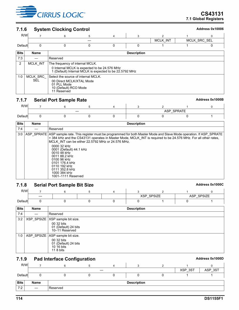
114 DS1155F1
CS431317.1 Global Registers
7.1.6 System Clocking Control Address 0x10006
R/W 7 6 5 4 3 2 1 0
— MCLK_INT MCLK_SRC_SEL
Default 0 0 0 0 0 1 1 0
Bits Name Description
7:3 — Reserved
2 MCLK_INT The frequency of internal MCLK.0 Internal MCLK is expected to be 24.576 MHz1 (Default) Internal MCLK is expected to be 22.5792 MHz
1:0 MCLK_SRC_SEL
Select the source of internal MCLK.00 Direct MCLK/XTAL Mode01 PLL Mode10 (Default) RCO Mode11 Reserved
7.1.7 Serial Port Sample Rate Address 0x1000B
R/W 7 6 5 4 3 2 1 0
— ASP_SPRATE
Default 0 0 0 0 0 0 0 1
Bits Name Description
7:4 — Reserved
3:0 ASP_SPRATE ASP sample rate. This register must be programmed for both Master Mode and Slave Mode operation. If ASP_SPRATE = 384 kHz and the CS43131 operates in Master Mode, MCLK_INT is required to be 24.576 MHz. For all other rates, MCLK_INT can be either 22.5792 MHz or 24.576 MHz.
0000 32 kHz0001 (Default) 44.1 kHz0010 48 kHz0011 88.2 kHz 0100 96 kHz0101 176.4 kHz0110 192 kHz0111 352.8 kHz1000 384 kHz1001–1111 Reserved
7.1.8 Serial Port Sample Bit Size Address 0x1000C
R/W 7 6 5 4 3 2 1 0
— XSP_SPSIZE ASP_SPSIZE
Default 0 0 0 0 0 1 0 1
Bits Name Description
7:4 — Reserved
3:2 XSP_SPSIZE XSP sample bit size.00 32 bits01 (Default) 24 bits10–11 Reserved
1:0 ASP_SPSIZE ASP sample bit size.00 32 bits01 (Default) 24 bits10 16 bits11 8 bits
7.1.9 Pad Interface Configuration Address 0x1000D
R/W 7 6 5 4 3 2 1 0
— XSP_3ST ASP_3ST
Default 0 0 0 0 0 0 1 1
Bits Name Description
7:2 — Reserved
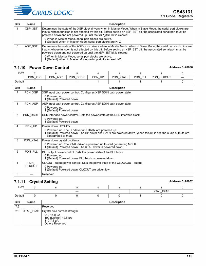
DS1155F1 115
CS431317.1 Global Registers
1 XSP_3ST Determines the state of the XSP clock drivers when in Master Mode. When in Slave Mode, the serial port clocks are inputs, whose function is not affected by this bit. Before setting an xSP_3ST bit, the associated serial port must be powered down and not powered up until the xSP_3ST bit is cleared.
0 When in Master Mode, serial port clocks are active.1 (Default) When in Master Mode, serial port clocks are Hi-Z.
0 ASP_3ST Determines the state of the ASP clock drivers when in Master Mode. When in Slave Mode, the serial port clock pins are inputs, whose function is not affected by this bit. Before setting an xSP_3ST bit, the associated serial port must be powered down and not powered up until the xSP_3ST bit is cleared.
0 When in Master Mode, serial port clocks are active.1 (Default) When in Master Mode, serial port clocks are Hi-Z.
7.1.10 Power Down Control Address 0x20000
R/W 7 6 5 4 3 2 1 0
PDN_XSP PDN_ASP PDN_DSDIF PDN_HP PDN_XTAL PDN_PLL PDN_CLKOUT —
Default 1 1 1 1 1 1 1 0
Bits Name Description
7 PDN_XSP XSP input path power control. Configures XSP SDIN path power state.0 Powered up.1 (Default) Powered down.
6 PDN_ASP ASP input path power control. Configures ASP SDIN path power state.0 Powered up.1 (Default) Powered down.
5 PDN_DSDIF DSD interface power control. Sets the power state of the DSD interface block.0 Powered up.1 (Default) Powered down.
4 PDN_HP Power down HPOUTx.0 Powered up. The HP driver and DACx are powered up.1 (Default) Powered down. The HP driver and DACx are powered down. When this bit is set, the audio outputs are
soft ramped to mute.
3 PDN_XTAL Power down crystal oscillator.0 Powered up. The XTAL driver is powered up to start generating MCLK.1 (Default) Powered down. The XTAL driver is powered down.
2 PDN_PLL PLL output power control. Sets the power state of the PLL block.0 Powered up.1 (Default) Powered down. PLL block is powered down.
1 PDN_CLKOUT
CLKOUT output power control. Sets the power state of the CLOCKOUT output.0 Powered up1 (Default) Powered down. CLKOUT are driven low.
0 — Reserved
7.1.11 Crystal Setting Address 0x20052
R/W 7 6 5 4 3 2 1 0
— XTAL_IBIAS
Default 0 0 0 0 0 1 0 0
Bits Name Description
7:3 — Reserved
2:0 XTAL_IBIAS Crystal bias current strength.010 15.0 µA100 (Default) 12.5 µA110 7.5 µAOthers Reserved
Bits Name Description
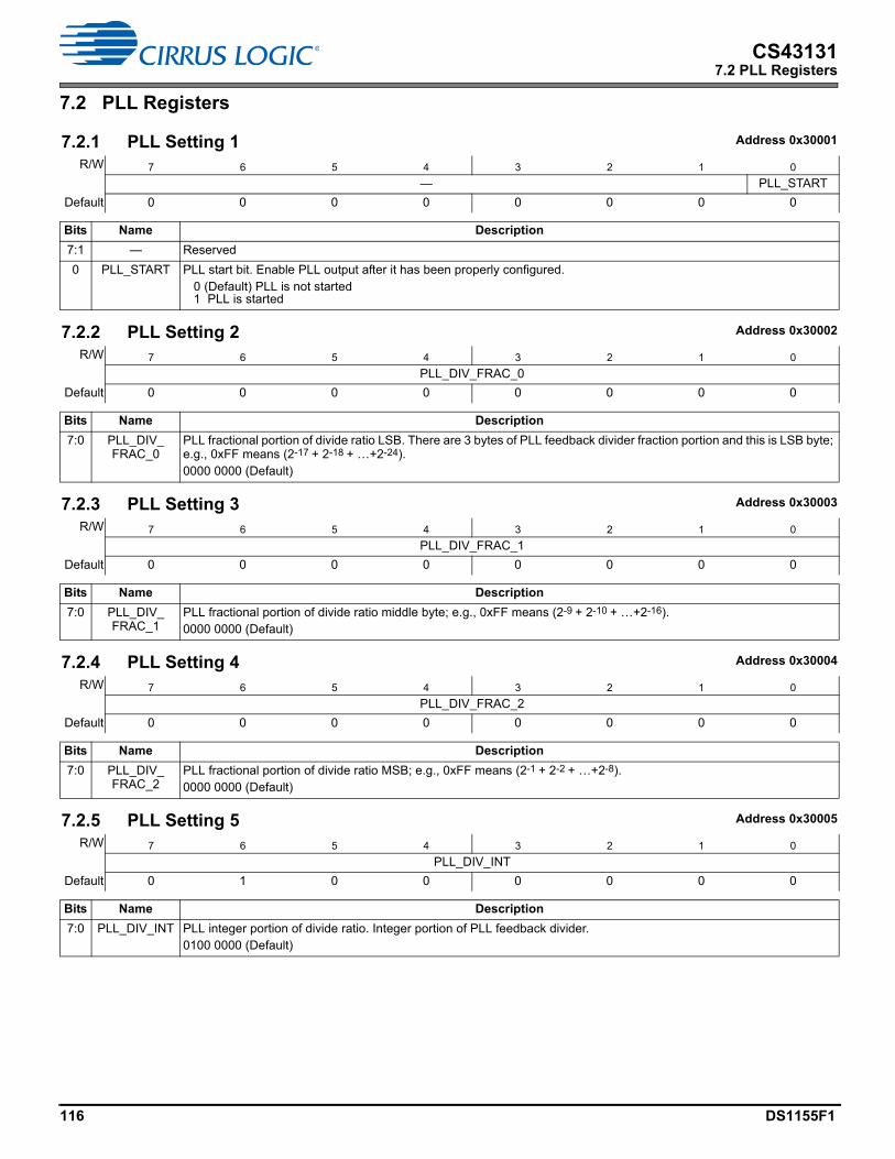
116 DS1155F1
CS431317.2 PLL Registers
7.2 PLL Registers
7.2.1 PLL Setting 1 Address 0x30001
R/W 7 6 5 4 3 2 1 0
— PLL_START
Default 0 0 0 0 0 0 0 0
Bits Name Description
7:1 — Reserved
0 PLL_START PLL start bit. Enable PLL output after it has been properly configured.0 (Default) PLL is not started1 PLL is started
7.2.2 PLL Setting 2 Address 0x30002
R/W 7 6 5 4 3 2 1 0
PLL_DIV_FRAC_0
Default 0 0 0 0 0 0 0 0
Bits Name Description
7:0 PLL_DIV_FRAC_0
PLL fractional portion of divide ratio LSB. There are 3 bytes of PLL feedback divider fraction portion and this is LSB byte; e.g., 0xFF means (2-17 + 2-18 + …+2-24).0000 0000 (Default)
7.2.3 PLL Setting 3 Address 0x30003
R/W 7 6 5 4 3 2 1 0
PLL_DIV_FRAC_1
Default 0 0 0 0 0 0 0 0
Bits Name Description
7:0 PLL_DIV_FRAC_1
PLL fractional portion of divide ratio middle byte; e.g., 0xFF means (2-9 + 2-10 + …+2-16).0000 0000 (Default)
7.2.4 PLL Setting 4 Address 0x30004
R/W 7 6 5 4 3 2 1 0
PLL_DIV_FRAC_2
Default 0 0 0 0 0 0 0 0
Bits Name Description
7:0 PLL_DIV_FRAC_2
PLL fractional portion of divide ratio MSB; e.g., 0xFF means (2-1 + 2-2 + …+2-8).0000 0000 (Default)
7.2.5 PLL Setting 5 Address 0x30005
R/W 7 6 5 4 3 2 1 0
PLL_DIV_INT
Default 0 1 0 0 0 0 0 0
Bits Name Description
7:0 PLL_DIV_INT PLL integer portion of divide ratio. Integer portion of PLL feedback divider.0100 0000 (Default)

DS1155F1 117
CS431317.2 PLL Registers
7.2.6 PLL Setting 6 Address 0x30008
R/W 7 6 5 4 3 2 1 0
PLL_OUT_DIV
Default 0 0 0 1 0 0 0 0
Bits Name Description
7:0 PLL_OUT_DIV
Final PLL clock output divide value. 0001 0000 (Default)
7.2.7 PLL Setting 7 Address 0x3000A
R/W 7 6 5 4 3 2 1 0
PLL_CAL_RATIO
Default 1 0 0 0 0 0 0 0
Bits Name Description
7:0 PLL_CAL_RATIO
PLL calibration ratio. See Section 4.7.2 for configuration details. Target value for PLL VCO calibration.1000 0000 (Default)
7.2.8 PLL Setting 8 Address 0x3001B
R/W 7 6 5 4 3 2 1 0
— PLL_MODE —
Default 0 0 0 1 0 0 1 1
Bits Name Description
7:2 — Reserved
1 PLL_MODE 500/512 factor used in PLL frequency calculation equation, Eq. 4-1.0 No bypass1 (Default) Bypass
0 — Reserved
7.2.9 PLL Setting 9 Address 0x40002
R/W 7 6 5 4 3 2 1 0
— PLL_REF_PREDIV
Default 0 0 0 0 0 0 1 0
Bits Name Description
7:2 — Reserved
1:0 PLL_REF_PREDIV
PLL reference divide select.00 Divide by 101 Divide by 210 (Default) Divide by 411 Divide by 8
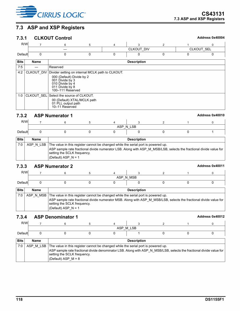
118 DS1155F1
CS431317.3 ASP and XSP Registers
7.3 ASP and XSP Registers
7.3.1 CLKOUT Control Address 0x40004
R/W 7 6 5 4 3 2 1 0
— CLKOUT_DIV CLKOUT_SEL
Default 0 0 0 0 0 0 0 0
Bits Name Description
7:5 — Reserved
4:2 CLKOUT_DIV Divider setting on internal MCLK path to CLKOUT.000 (Default) Divide by 2001 Divide by 3010 Divide by 4011 Divide by 8100–111 Reserved
1:0 CLKOUT_SEL Select the source of CLKOUT.00 (Default) XTAL/MCLK path01 PLL output path10–11 Reserved
7.3.2 ASP Numerator 1 Address 0x40010
R/W 7 6 5 4 3 2 1 0
ASP_N_LSB
Default 0 0 0 0 0 0 0 1
Bits Name Description
7:0 ASP_N_LSB The value in this register cannot be changed while the serial port is powered up. ASP sample rate fractional divide numerator LSB. Along with ASP_M_MSB/LSB, selects the fractional divide value for setting the SCLK frequency.(Default) ASP_N = 1
7.3.3 ASP Numerator 2 Address 0x40011
R/W 7 6 5 4 3 2 1 0
ASP_N_MSB
Default 0 0 0 0 0 0 0 0
Bits Name Description
7:0 ASP_N_MSB The value in this register cannot be changed while the serial port is powered up. ASP sample rate fractional divide numerator MSB. Along with ASP_M_MSB/LSB, selects the fractional divide value for setting the SCLK frequency.(Default) ASP_N = 1
7.3.4 ASP Denominator 1 Address 0x40012
R/W 7 6 5 4 3 2 1 0
ASP_M_LSB
Default 0 0 0 0 1 0 0 0
Bits Name Description
7:0 ASP_M_LSB The value in this register cannot be changed while the serial port is powered up. ASP sample rate fractional divide denominator LSB. Along with ASP_N_MSB/LSB, selects the fractional divide value for setting the SCLK frequency.(Default) ASP_M = 8
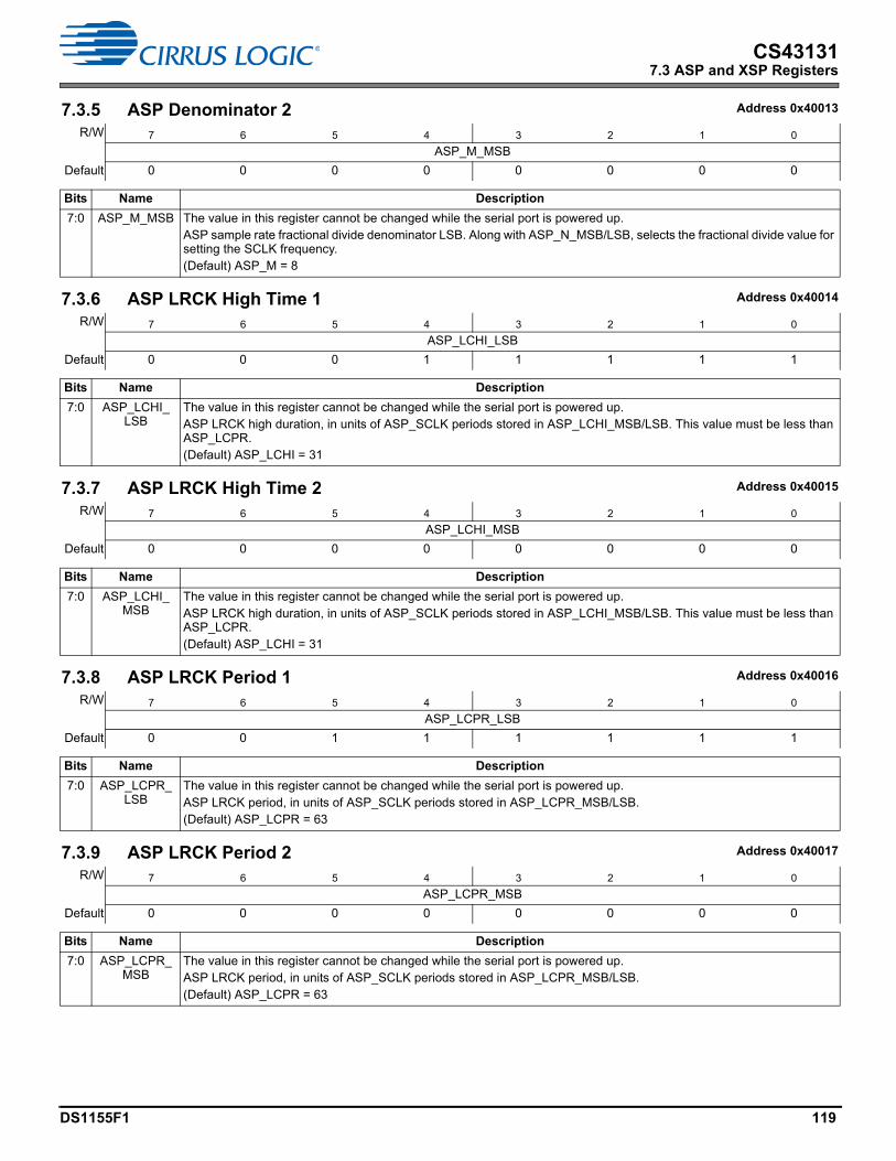
DS1155F1 119
CS431317.3 ASP and XSP Registers
7.3.5 ASP Denominator 2 Address 0x40013
R/W 7 6 5 4 3 2 1 0
ASP_M_MSB
Default 0 0 0 0 0 0 0 0
Bits Name Description
7:0 ASP_M_MSB The value in this register cannot be changed while the serial port is powered up. ASP sample rate fractional divide denominator LSB. Along with ASP_N_MSB/LSB, selects the fractional divide value for setting the SCLK frequency.(Default) ASP_M = 8
7.3.6 ASP LRCK High Time 1 Address 0x40014
R/W 7 6 5 4 3 2 1 0
ASP_LCHI_LSB
Default 0 0 0 1 1 1 1 1
Bits Name Description
7:0 ASP_LCHI_LSB
The value in this register cannot be changed while the serial port is powered up. ASP LRCK high duration, in units of ASP_SCLK periods stored in ASP_LCHI_MSB/LSB. This value must be less than ASP_LCPR.(Default) ASP_LCHI = 31
7.3.7 ASP LRCK High Time 2 Address 0x40015
R/W 7 6 5 4 3 2 1 0
ASP_LCHI_MSB
Default 0 0 0 0 0 0 0 0
Bits Name Description
7:0 ASP_LCHI_MSB
The value in this register cannot be changed while the serial port is powered up. ASP LRCK high duration, in units of ASP_SCLK periods stored in ASP_LCHI_MSB/LSB. This value must be less than ASP_LCPR.(Default) ASP_LCHI = 31
7.3.8 ASP LRCK Period 1 Address 0x40016
R/W 7 6 5 4 3 2 1 0
ASP_LCPR_LSB
Default 0 0 1 1 1 1 1 1
Bits Name Description
7:0 ASP_LCPR_LSB
The value in this register cannot be changed while the serial port is powered up. ASP LRCK period, in units of ASP_SCLK periods stored in ASP_LCPR_MSB/LSB.(Default) ASP_LCPR = 63
7.3.9 ASP LRCK Period 2 Address 0x40017
R/W 7 6 5 4 3 2 1 0
ASP_LCPR_MSB
Default 0 0 0 0 0 0 0 0
Bits Name Description
7:0 ASP_LCPR_MSB
The value in this register cannot be changed while the serial port is powered up. ASP LRCK period, in units of ASP_SCLK periods stored in ASP_LCPR_MSB/LSB.(Default) ASP_LCPR = 63
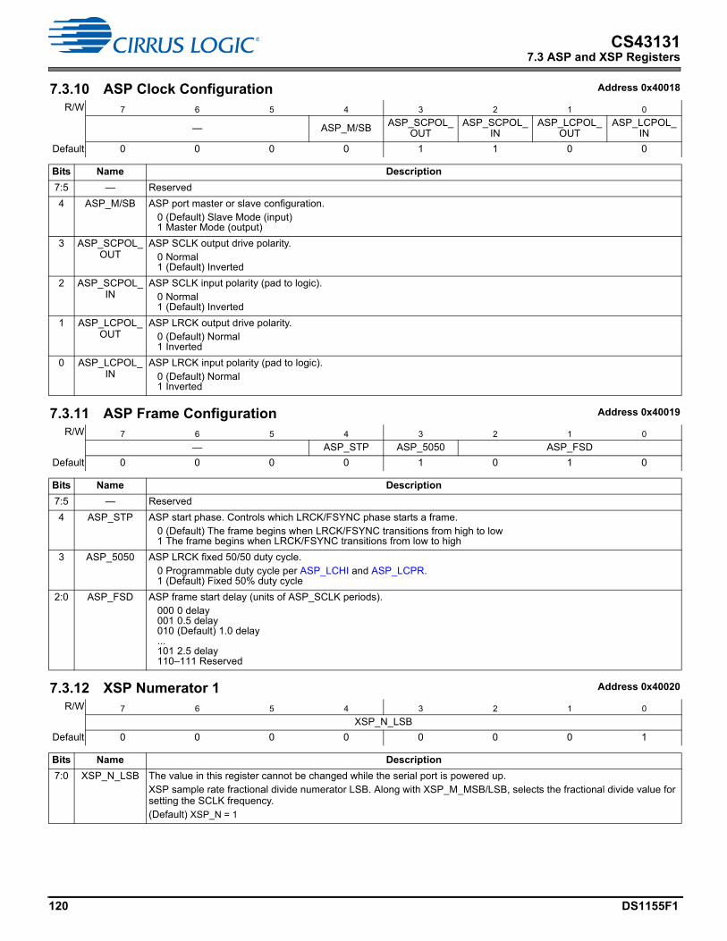
120 DS1155F1
CS431317.3 ASP and XSP Registers
7.3.10 ASP Clock Configuration Address 0x40018
R/W 7 6 5 4 3 2 1 0
— ASP_M/SB ASP_SCPOL_OUT
ASP_SCPOL_IN
ASP_LCPOL_OUT
ASP_LCPOL_IN
Default 0 0 0 0 1 1 0 0
Bits Name Description
7:5 — Reserved
4 ASP_M/SB ASP port master or slave configuration.0 (Default) Slave Mode (input)1 Master Mode (output)
3 ASP_SCPOL_OUT
ASP SCLK output drive polarity.0 Normal1 (Default) Inverted
2 ASP_SCPOL_IN
ASP SCLK input polarity (pad to logic).0 Normal1 (Default) Inverted
1 ASP_LCPOL_OUT
ASP LRCK output drive polarity.0 (Default) Normal1 Inverted
0 ASP_LCPOL_IN
ASP LRCK input polarity (pad to logic).0 (Default) Normal1 Inverted
7.3.11 ASP Frame Configuration Address 0x40019
R/W 7 6 5 4 3 2 1 0
— ASP_STP ASP_5050 ASP_FSD
Default 0 0 0 0 1 0 1 0
Bits Name Description
7:5 — Reserved
4 ASP_STP ASP start phase. Controls which LRCK/FSYNC phase starts a frame.0 (Default) The frame begins when LRCK/FSYNC transitions from high to low1 The frame begins when LRCK/FSYNC transitions from low to high
3 ASP_5050 ASP LRCK fixed 50/50 duty cycle.0 Programmable duty cycle per ASP_LCHI and ASP_LCPR.1 (Default) Fixed 50% duty cycle
2:0 ASP_FSD ASP frame start delay (units of ASP_SCLK periods).000 0 delay001 0.5 delay010 (Default) 1.0 delay...101 2.5 delay110–111 Reserved
7.3.12 XSP Numerator 1 Address 0x40020
R/W 7 6 5 4 3 2 1 0
XSP_N_LSB
Default 0 0 0 0 0 0 0 1
Bits Name Description
7:0 XSP_N_LSB The value in this register cannot be changed while the serial port is powered up. XSP sample rate fractional divide numerator LSB. Along with XSP_M_MSB/LSB, selects the fractional divide value for setting the SCLK frequency.(Default) XSP_N = 1
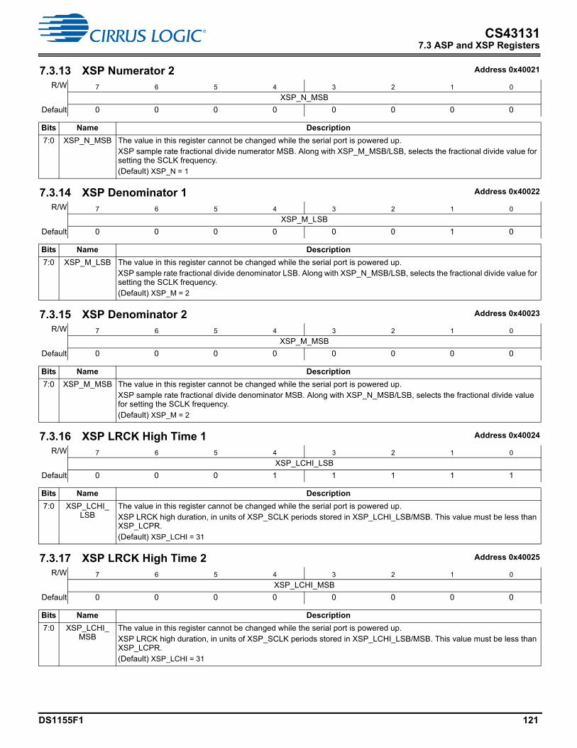
DS1155F1 121
CS431317.3 ASP and XSP Registers
7.3.13 XSP Numerator 2 Address 0x40021
R/W 7 6 5 4 3 2 1 0
XSP_N_MSB
Default 0 0 0 0 0 0 0 0
Bits Name Description
7:0 XSP_N_MSB The value in this register cannot be changed while the serial port is powered up. XSP sample rate fractional divide numerator MSB. Along with XSP_M_MSB/LSB, selects the fractional divide value for setting the SCLK frequency.(Default) XSP_N = 1
7.3.14 XSP Denominator 1 Address 0x40022
R/W 7 6 5 4 3 2 1 0
XSP_M_LSB
Default 0 0 0 0 0 0 1 0
Bits Name Description
7:0 XSP_M_LSB The value in this register cannot be changed while the serial port is powered up. XSP sample rate fractional divide denominator LSB. Along with XSP_N_MSB/LSB, selects the fractional divide value for setting the SCLK frequency.(Default) XSP_M = 2
7.3.15 XSP Denominator 2 Address 0x40023
R/W 7 6 5 4 3 2 1 0
XSP_M_MSB
Default 0 0 0 0 0 0 0 0
Bits Name Description
7:0 XSP_M_MSB The value in this register cannot be changed while the serial port is powered up. XSP sample rate fractional divide denominator MSB. Along with XSP_N_MSB/LSB, selects the fractional divide value for setting the SCLK frequency.(Default) XSP_M = 2
7.3.16 XSP LRCK High Time 1 Address 0x40024
R/W 7 6 5 4 3 2 1 0
XSP_LCHI_LSB
Default 0 0 0 1 1 1 1 1
Bits Name Description
7:0 XSP_LCHI_LSB
The value in this register cannot be changed while the serial port is powered up. XSP LRCK high duration, in units of XSP_SCLK periods stored in XSP_LCHI_LSB/MSB. This value must be less than XSP_LCPR.(Default) XSP_LCHI = 31
7.3.17 XSP LRCK High Time 2 Address 0x40025
R/W 7 6 5 4 3 2 1 0
XSP_LCHI_MSB
Default 0 0 0 0 0 0 0 0
Bits Name Description
7:0 XSP_LCHI_MSB
The value in this register cannot be changed while the serial port is powered up. XSP LRCK high duration, in units of XSP_SCLK periods stored in XSP_LCHI_LSB/MSB. This value must be less than XSP_LCPR.(Default) XSP_LCHI = 31
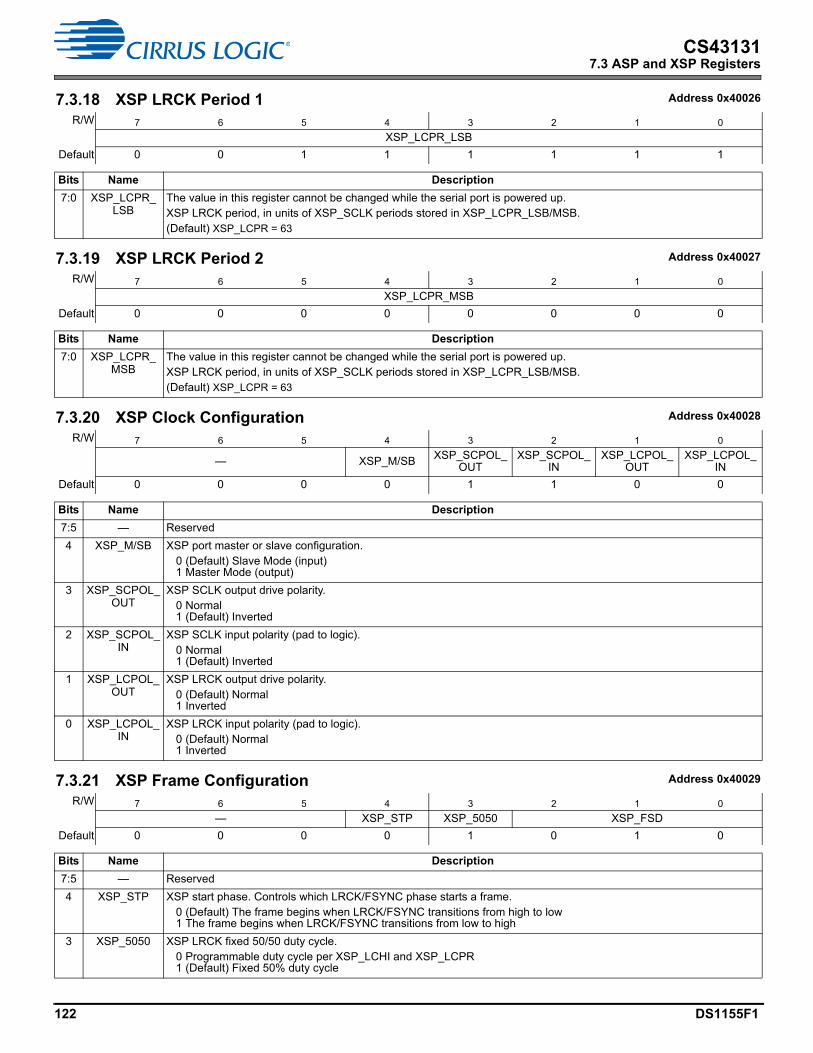
122 DS1155F1
CS431317.3 ASP and XSP Registers
7.3.18 XSP LRCK Period 1 Address 0x40026
R/W 7 6 5 4 3 2 1 0
XSP_LCPR_LSB
Default 0 0 1 1 1 1 1 1
Bits Name Description
7:0 XSP_LCPR_LSB
The value in this register cannot be changed while the serial port is powered up. XSP LRCK period, in units of XSP_SCLK periods stored in XSP_LCPR_LSB/MSB.(Default) XSP_LCPR = 63
7.3.19 XSP LRCK Period 2 Address 0x40027
R/W 7 6 5 4 3 2 1 0
XSP_LCPR_MSB
Default 0 0 0 0 0 0 0 0
Bits Name Description
7:0 XSP_LCPR_MSB
The value in this register cannot be changed while the serial port is powered up. XSP LRCK period, in units of XSP_SCLK periods stored in XSP_LCPR_LSB/MSB.(Default) XSP_LCPR = 63
7.3.20 XSP Clock Configuration Address 0x40028
R/W 7 6 5 4 3 2 1 0
— XSP_M/SB XSP_SCPOL_OUT
XSP_SCPOL_IN
XSP_LCPOL_OUT
XSP_LCPOL_IN
Default 0 0 0 0 1 1 0 0
Bits Name Description
7:5 — Reserved
4 XSP_M/SB XSP port master or slave configuration.0 (Default) Slave Mode (input)1 Master Mode (output)
3 XSP_SCPOL_OUT
XSP SCLK output drive polarity.0 Normal1 (Default) Inverted
2 XSP_SCPOL_IN
XSP SCLK input polarity (pad to logic).0 Normal1 (Default) Inverted
1 XSP_LCPOL_OUT
XSP LRCK output drive polarity.0 (Default) Normal1 Inverted
0 XSP_LCPOL_IN
XSP LRCK input polarity (pad to logic).0 (Default) Normal1 Inverted
7.3.21 XSP Frame Configuration Address 0x40029
R/W 7 6 5 4 3 2 1 0
— XSP_STP XSP_5050 XSP_FSD
Default 0 0 0 0 1 0 1 0
Bits Name Description
7:5 — Reserved
4 XSP_STP XSP start phase. Controls which LRCK/FSYNC phase starts a frame.0 (Default) The frame begins when LRCK/FSYNC transitions from high to low1 The frame begins when LRCK/FSYNC transitions from low to high
3 XSP_5050 XSP LRCK fixed 50/50 duty cycle.0 Programmable duty cycle per XSP_LCHI and XSP_LCPR1 (Default) Fixed 50% duty cycle
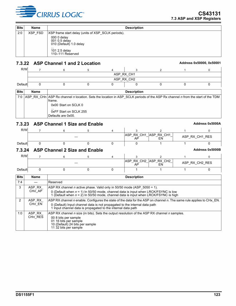
DS1155F1 123
CS431317.3 ASP and XSP Registers
2:0 XSP_FSD XSP frame start delay (units of XSP_SCLK periods).000 0 delay001 0.5 delay010 (Default) 1.0 delay...101 2.5 delay110–111 Reserved
7.3.22 ASP Channel 1 and 2 Location Address 0x50000, 0x50001
R/W 7 6 5 4 3 2 1 0
ASP_RX_CH1
ASP_RX_CH2
Default 0 0 0 0 0 0 0 0
Bits Name Description
7:0 ASP_RX_CHn ASP Rx channel n location. Sets the location in ASP_SCLK periods of the ASP Rx channel n from the start of the TDM frame.
0x00 Start on SCLK 0...0xFF Start on SCLK 255
Defaults are 0x00.
7.3.23 ASP Channel 1 Size and Enable Address 0x5000A
R/W 7 6 5 4 3 2 1 0
— ASP_RX_CH1_AP
ASP_RX_CH1_EN ASP_RX_CH1_RES
Default 0 0 0 0 0 1 1 0
7.3.24 ASP Channel 2 Size and Enable Address 0x5000B
R/W 7 6 5 4 3 2 1 0
— ASP_RX_CH2_AP
ASP_RX_CH2_EN ASP_RX_CH2_RES
Default 0 0 0 0 1 1 1 0
Bits Name Description
7:4 — Reserved
3 ASP_RX_CHn_AP
ASP RX channel n active phase. Valid only in 50/50 mode (ASP_5050 = 1).0 (Default when n = 1) In 50/50 mode, channel data is input when LRCK/FSYNC is low1 (Default when n = 2) In 50/50 mode, channel data is input when LRCK/FSYNC is high
2 ASP_RX_CHn_EN
ASP RX channel n enable. Configures the state of the data for the ASP on channel n. The same rule applies to CHx_EN. 0 (Default) Input channel data is not propagated to the internal data path1 Input channel data is propagated to the internal data path
1:0 ASP_RX_CHn_RES
ASP RX channel n size (in bits). Sets the output resolution of the ASP RX channel n samples.00 8 bits per sample01 16 bits per sample10 (Default) 24 bits per sample11 32 bits per sample
Bits Name Description
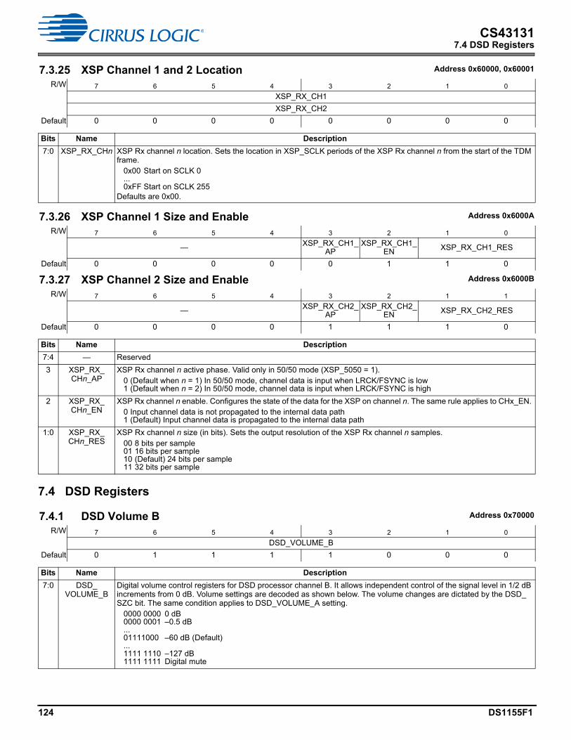
124 DS1155F1
CS431317.4 DSD Registers
7.4 DSD Registers
7.3.25 XSP Channel 1 and 2 Location Address 0x60000, 0x60001
R/W 7 6 5 4 3 2 1 0
XSP_RX_CH1
XSP_RX_CH2
Default 0 0 0 0 0 0 0 0
Bits Name Description
7:0 XSP_RX_CHn XSP Rx channel n location. Sets the location in XSP_SCLK periods of the XSP Rx channel n from the start of the TDM frame.
0x00 Start on SCLK 0...0xFF Start on SCLK 255
Defaults are 0x00.
7.3.26 XSP Channel 1 Size and Enable Address 0x6000A
R/W 7 6 5 4 3 2 1 0
— XSP_RX_CH1_AP
XSP_RX_CH1_EN XSP_RX_CH1_RES
Default 0 0 0 0 0 1 1 0
7.3.27 XSP Channel 2 Size and Enable Address 0x6000B
R/W 7 6 5 4 3 2 1 1
— XSP_RX_CH2_AP
XSP_RX_CH2_EN XSP_RX_CH2_RES
Default 0 0 0 0 1 1 1 0
Bits Name Description
7:4 — Reserved
3 XSP_RX_CHn_AP
XSP Rx channel n active phase. Valid only in 50/50 mode (XSP_5050 = 1).0 (Default when n = 1) In 50/50 mode, channel data is input when LRCK/FSYNC is low1 (Default when n = 2) In 50/50 mode, channel data is input when LRCK/FSYNC is high
2 XSP_RX_CHn_EN
XSP Rx channel n enable. Configures the state of the data for the XSP on channel n. The same rule applies to CHx_EN. 0 Input channel data is not propagated to the internal data path1 (Default) Input channel data is propagated to the internal data path
1:0 XSP_RX_CHn_RES
XSP Rx channel n size (in bits). Sets the output resolution of the XSP Rx channel n samples.00 8 bits per sample01 16 bits per sample10 (Default) 24 bits per sample11 32 bits per sample
7.4.1 DSD Volume B Address 0x70000
R/W 7 6 5 4 3 2 1 0
DSD_VOLUME_B
Default 0 1 1 1 1 0 0 0
Bits Name Description
7:0 DSD_VOLUME_B
Digital volume control registers for DSD processor channel B. It allows independent control of the signal level in 1/2 dB increments from 0 dB. Volume settings are decoded as shown below. The volume changes are dictated by the DSD_SZC bit. The same condition applies to DSD_VOLUME_A setting.
0000 0000 0 dB0000 0001 –0.5 dB...01111000 –60 dB (Default)...1111 1110 –127 dB1111 1111 Digital mute
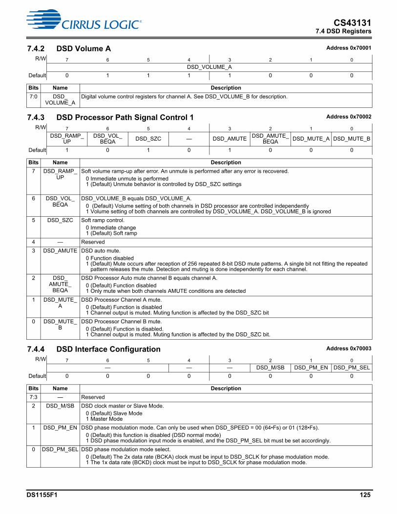
DS1155F1 125
CS431317.4 DSD Registers
7.4.2 DSD Volume A Address 0x70001
R/W 7 6 5 4 3 2 1 0
DSD_VOLUME_A
Default 0 1 1 1 1 0 0 0
Bits Name Description
7:0 DSD_VOLUME_A
Digital volume control registers for channel A. See DSD_VOLUME_B for description.
7.4.3 DSD Processor Path Signal Control 1 Address 0x70002
R/W 7 6 5 4 3 2 1 0
DSD_RAMP_UP
DSD_VOL_BEQA DSD_SZC — DSD_AMUTE DSD_AMUTE_
BEQA DSD_MUTE_A DSD_MUTE_B
Default 1 0 1 0 1 0 0 0
Bits Name Description
7 DSD_RAMP_UP
Soft volume ramp-up after error. An unmute is performed after any error is recovered. 0 Immediate unmute is performed1 (Default) Unmute behavior is controlled by DSD_SZC settings
6 DSD_VOL_BEQA
DSD_VOLUME_B equals DSD_VOLUME_A.0 (Default) Volume setting of both channels in DSD processor are controlled independently1 Volume setting of both channels are controlled by DSD_VOLUME_A. DSD_VOLUME_B is ignored
5 DSD_SZC Soft ramp control.0 Immediate change1 (Default) Soft ramp
4 — Reserved
3 DSD_AMUTE DSD auto mute.0 Function disabled1 (Default) Mute occurs after reception of 256 repeated 8-bit DSD mute patterns. A single bit not fitting the repeated
pattern releases the mute. Detection and muting is done independently for each channel.
2 DSD_AMUTE_
BEQA
DSD Processor Auto mute channel B equals channel A.0 (Default) Function disabled1 Only mute when both channels AMUTE conditions are detected
1 DSD_MUTE_A
DSD Processor Channel A mute.0 (Default) Function is disabled1 Channel output is muted. Muting function is affected by the DSD_SZC bit
0 DSD_MUTE_B
DSD Processor Channel B mute.0 (Default) Function is disabled.1 Channel output is muted. Muting function is affected by the DSD_SZC bit.
7.4.4 DSD Interface Configuration Address 0x70003
R/W 7 6 5 4 3 2 1 0
— — — DSD_M/SB DSD_PM_EN DSD_PM_SEL
Default 0 0 0 0 0 0 0 0
Bits Name Description
7:3 — Reserved
2 DSD_M/SB DSD clock master or Slave Mode.0 (Default) Slave Mode1 Master Mode
1 DSD_PM_EN DSD phase modulation mode. Can only be used when DSD_SPEED = 00 (64•Fs) or 01 (128•Fs).0 (Default) this function is disabled (DSD normal mode)1 DSD phase modulation input mode is enabled, and the DSD_PM_SEL bit must be set accordingly.
0 DSD_PM_SEL DSD phase modulation mode select.0 (Default) The 2x data rate (BCKA) clock must be input to DSD_SCLK for phase modulation mode.1 The 1x data rate (BCKD) clock must be input to DSD_SCLK for phase modulation mode.
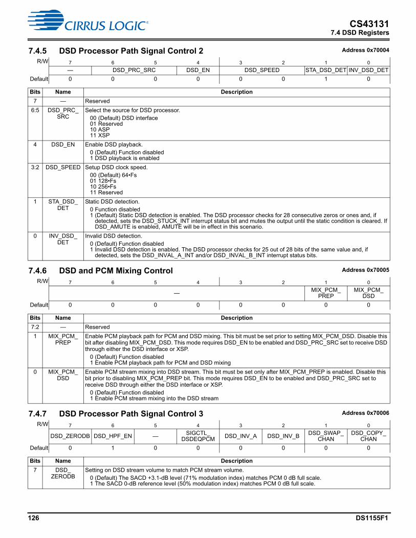
126 DS1155F1
CS431317.4 DSD Registers
7.4.5 DSD Processor Path Signal Control 2 Address 0x70004
R/W 7 6 5 4 3 2 1 0
— DSD_PRC_SRC DSD_EN DSD_SPEED STA_DSD_DET INV_DSD_DET
Default 0 0 0 0 0 0 1 0
Bits Name Description
7 — Reserved
6:5 DSD_PRC_SRC
Select the source for DSD processor.00 (Default) DSD interface01 Reserved10 ASP11 XSP
4 DSD_EN Enable DSD playback.0 (Default) Function disabled1 DSD playback is enabled
3:2 DSD_SPEED Setup DSD clock speed. 00 (Default) 64•Fs01 128•Fs 10 256•Fs11 Reserved
1 STA_DSD_DET
Static DSD detection.0 Function disabled1 (Default) Static DSD detection is enabled. The DSD processor checks for 28 consecutive zeros or ones and, if
detected, sets the DSD_STUCK_INT interrupt status bit and mutes the output until the static condition is cleared. If DSD_AMUTE is enabled, AMUTE will be in effect in this scenario.
0 INV_DSD_DET
Invalid DSD detection.0 (Default) Function disabled1 Invalid DSD detection is enabled. The DSD processor checks for 25 out of 28 bits of the same value and, if
detected, sets the DSD_INVAL_A_INT and/or DSD_INVAL_B_INT interrupt status bits.
7.4.6 DSD and PCM Mixing Control Address 0x70005
R/W 7 6 5 4 3 2 1 0
— MIX_PCM_PREP
MIX_PCM_DSD
Default 0 0 0 0 0 0 0 0
Bits Name Description
7:2 — Reserved
1 MIX_PCM_PREP
Enable PCM playback path for PCM and DSD mixing. This bit must be set prior to setting MIX_PCM_DSD. Disable this bit after disabling MIX_PCM_DSD. This mode requires DSD_EN to be enabled and DSD_PRC_SRC set to receive DSD through either the DSD interface or XSP.
0 (Default) Function disabled1 Enable PCM playback path for PCM and DSD mixing
0 MIX_PCM_DSD
Enable PCM stream mixing into DSD stream. This bit must be set only after MIX_PCM_PREP is enabled. Disable this bit prior to disabling MIX_PCM_PREP bit. This mode requires DSD_EN to be enabled and DSD_PRC_SRC set to receive DSD through either the DSD interface or XSP.
0 (Default) Function disabled1 Enable PCM stream mixing into the DSD stream
7.4.7 DSD Processor Path Signal Control 3 Address 0x70006
R/W 7 6 5 4 3 2 1 0
DSD_ZERODB DSD_HPF_EN — SIGCTL_DSDEQPCM DSD_INV_A DSD_INV_B DSD_SWAP_
CHANDSD_COPY_
CHAN
Default 0 1 0 0 0 0 0 0
Bits Name Description
7 DSD_ZERODB
Setting on DSD stream volume to match PCM stream volume.0 (Default) The SACD +3.1-dB level (71% modulation index) matches PCM 0 dB full scale.1 The SACD 0-dB reference level (50% modulation index) matches PCM 0 dB full scale.
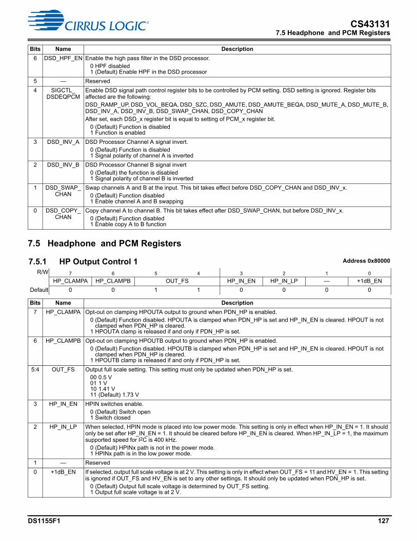
DS1155F1 127
CS431317.5 Headphone and PCM Registers
7.5 Headphone and PCM Registers
6 DSD_HPF_EN Enable the high pass filter in the DSD processor. 0 HPF disabled1 (Default) Enable HPF in the DSD processor
5 — Reserved
4 SIGCTL_DSDEQPCM
Enable DSD signal path control register bits to be controlled by PCM setting. DSD setting is ignored. Register bits affected are the following:DSD_RAMP_UP, DSD_VOL_BEQA, DSD_SZC, DSD_AMUTE, DSD_AMUTE_BEQA, DSD_MUTE_A, DSD_MUTE_B, DSD_INV_A, DSD_INV_B, DSD_SWAP_CHAN, DSD_COPY_CHANAfter set, each DSD_x register bit is equal to setting of PCM_x register bit.
0 (Default) Function is disabled1 Function is enabled
3 DSD_INV_A DSD Processor Channel A signal invert.0 (Default) Function is disabled1 Signal polarity of channel A is inverted
2 DSD_INV_B DSD Processor Channel B signal invert0 (Default) the function is disabled1 Signal polarity of channel B is inverted
1 DSD_SWAP_CHAN
Swap channels A and B at the input. This bit takes effect before DSD_COPY_CHAN and DSD_INV_x.0 (Default) Function disabled1 Enable channel A and B swapping
0 DSD_COPY_CHAN
Copy channel A to channel B. This bit takes effect after DSD_SWAP_CHAN, but before DSD_INV_x.0 (Default) Function disabled1 Enable copy A to B function
7.5.1 HP Output Control 1 Address 0x80000
R/W 7 6 5 4 3 2 1 0
HP_CLAMPA HP_CLAMPB OUT_FS HP_IN_EN HP_IN_LP — +1dB_EN
Default 0 0 1 1 0 0 0 0
Bits Name Description
7 HP_CLAMPA Opt-out on clamping HPOUTA output to ground when PDN_HP is enabled.0 (Default) Function disabled. HPOUTA is clamped when PDN_HP is set and HP_IN_EN is cleared. HPOUT is not
clamped when PDN_HP is cleared. 1 HPOUTA clamp is released if and only if PDN_HP is set.
6 HP_CLAMPB Opt-out on clamping HPOUTB output to ground when PDN_HP is enabled.0 (Default) Function disabled. HPOUTB is clamped when PDN_HP is set and HP_IN_EN is cleared. HPOUT is not
clamped when PDN_HP is cleared. 1 HPOUTB clamp is released if and only if PDN_HP is set.
5:4 OUT_FS Output full scale setting. This setting must only be updated when PDN_HP is set.00 0.5 V 01 1 V 10 1.41 V11 (Default) 1.73 V
3 HP_IN_EN HPIN switches enable.0 (Default) Switch open1 Switch closed
2 HP_IN_LP When selected, HPIN mode is placed into low power mode. This setting is only in effect when HP_IN_EN = 1. It should only be set after HP_IN_EN = 1. It should be cleared before HP_IN_EN is cleared. When HP_IN_LP = 1, the maximum supported speed for I2C is 400 kHz.
0 (Default) HPINx path is not in the power mode.1 HPINx path is in the low power mode.
1 — Reserved
0 +1dB_EN If selected, output full scale voltage is at 2 V. This setting is only in effect when OUT_FS = 11 and HV_EN = 1. This setting is ignored if OUT_FS and HV_EN is set to any other settings. It should only be updated when PDN_HP is set.
0 (Default) Output full scale voltage is determined by OUT_FS setting.1 Output full scale voltage is at 2 V.
Bits Name Description
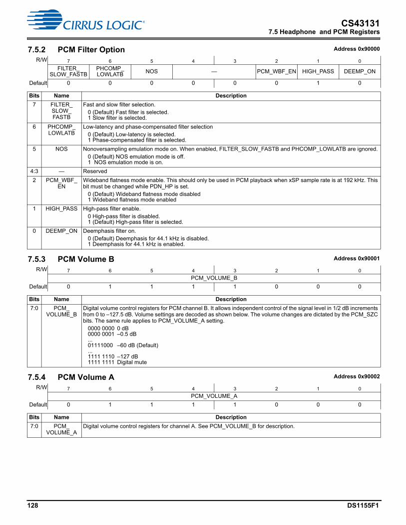
128 DS1155F1
CS431317.5 Headphone and PCM Registers
7.5.2 PCM Filter Option Address 0x90000
R/W 7 6 5 4 3 2 1 0
FILTER_SLOW_FASTB
PHCOMP_LOWLATB NOS — PCM_WBF_EN HIGH_PASS DEEMP_ON
Default 0 0 0 0 0 0 1 0
Bits Name Description
7 FILTER_SLOW_FASTB
Fast and slow filter selection.0 (Default) Fast filter is selected.1 Slow filter is selected.
6 PHCOMP_LOWLATB
Low-latency and phase-compensated filter selection0 (Default) Low-latency is selected.1 Phase-compensated filter is selected.
5 NOS Nonoversampling emulation mode on. When enabled, FILTER_SLOW_FASTB and PHCOMP_LOWLATB are ignored.0 (Default) NOS emulation mode is off.1 NOS emulation mode is on.
4:3 — Reserved
2 PCM_WBF_EN
Wideband flatness mode enable. This should only be used in PCM playback when xSP sample rate is at 192 kHz. This bit must be changed while PDN_HP is set.
0 (Default) Wideband flatness mode disabled1 Wideband flatness mode enabled
1 HIGH_PASS High-pass filter enable.0 High-pass filter is disabled. 1 (Default) High-pass filter is selected.
0 DEEMP_ON Deemphasis filter on.0 (Default) Deemphasis for 44.1 kHz is disabled.1 Deemphasis for 44.1 kHz is enabled.
7.5.3 PCM Volume B Address 0x90001
R/W 7 6 5 4 3 2 1 0
PCM_VOLUME_B
Default 0 1 1 1 1 0 0 0
Bits Name Description
7:0 PCM_VOLUME_B
Digital volume control registers for PCM channel B. It allows independent control of the signal level in 1/2 dB increments from 0 to –127.5 dB. Volume settings are decoded as shown below. The volume changes are dictated by the PCM_SZC bits. The same rule applies to PCM_VOLUME_A setting.
0000 0000 0 dB0000 0001 –0.5 dB...01111000 –60 dB (Default)...1111 1110 –127 dB1111 1111 Digital mute
7.5.4 PCM Volume A Address 0x90002
R/W 7 6 5 4 3 2 1 0
PCM_VOLUME_A
Default 0 1 1 1 1 0 0 0
Bits Name Description
7:0 PCM_VOLUME_A
Digital volume control registers for channel A. See PCM_VOLUME_B for description.
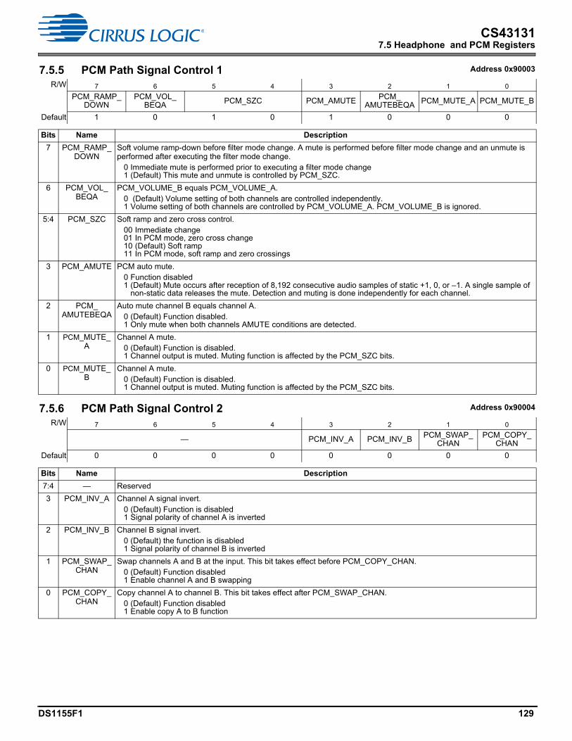
DS1155F1 129
CS431317.5 Headphone and PCM Registers
7.5.5 PCM Path Signal Control 1 Address 0x90003
R/W 7 6 5 4 3 2 1 0
PCM_RAMP_DOWN
PCM_VOL_BEQA PCM_SZC PCM_AMUTE PCM_
AMUTEBEQA PCM_MUTE_A PCM_MUTE_B
Default 1 0 1 0 1 0 0 0
Bits Name Description
7 PCM_RAMP_DOWN
Soft volume ramp-down before filter mode change. A mute is performed before filter mode change and an unmute is performed after executing the filter mode change.
0 Immediate mute is performed prior to executing a filter mode change1 (Default) This mute and unmute is controlled by PCM_SZC.
6 PCM_VOL_BEQA
PCM_VOLUME_B equals PCM_VOLUME_A.0 (Default) Volume setting of both channels are controlled independently.1 Volume setting of both channels are controlled by PCM_VOLUME_A. PCM_VOLUME_B is ignored.
5:4 PCM_SZC Soft ramp and zero cross control.00 Immediate change01 In PCM mode, zero cross change10 (Default) Soft ramp11 In PCM mode, soft ramp and zero crossings
3 PCM_AMUTE PCM auto mute.0 Function disabled1 (Default) Mute occurs after reception of 8,192 consecutive audio samples of static +1, 0, or –1. A single sample of
non-static data releases the mute. Detection and muting is done independently for each channel.
2 PCM_AMUTEBEQA
Auto mute channel B equals channel A.0 (Default) Function disabled. 1 Only mute when both channels AMUTE conditions are detected.
1 PCM_MUTE_A
Channel A mute.0 (Default) Function is disabled.1 Channel output is muted. Muting function is affected by the PCM_SZC bits.
0 PCM_MUTE_B
Channel A mute.0 (Default) Function is disabled.1 Channel output is muted. Muting function is affected by the PCM_SZC bits.
7.5.6 PCM Path Signal Control 2 Address 0x90004
R/W 7 6 5 4 3 2 1 0
— PCM_INV_A PCM_INV_B PCM_SWAP_CHAN
PCM_COPY_CHAN
Default 0 0 0 0 0 0 0 0
Bits Name Description
7:4 — Reserved
3 PCM_INV_A Channel A signal invert.0 (Default) Function is disabled1 Signal polarity of channel A is inverted
2 PCM_INV_B Channel B signal invert.0 (Default) the function is disabled1 Signal polarity of channel B is inverted
1 PCM_SWAP_CHAN
Swap channels A and B at the input. This bit takes effect before PCM_COPY_CHAN.0 (Default) Function disabled1 Enable channel A and B swapping
0 PCM_COPY_CHAN
Copy channel A to channel B. This bit takes effect after PCM_SWAP_CHAN.0 (Default) Function disabled1 Enable copy A to B function

130 DS1155F1
CS431317.5 Headphone and PCM Registers
7.5.7 Programmable Filter Control 1 Address 0x9 000A
R/W 7 6 5 4 3 2 1 0
SOS1_CTRL SOS2_CTRL FOS_CTRL SOS3_ON —
Default 0 0 0 0 0 0 0 0
Bits Name Description
7:6 SOS1_CTRL SOS1 filter control.00 SOS1 filter disabled. 01 Reserved. 10 Reserved. 11 SOS1 filter enabled.
5:4 SOS2_CTRL SOS2 filter control.00 SOS2 filter disabled. 01 Reserved. 10 Reserved. 11 SOS2 filter enabled.
3:2 FOS_CTRL FOS filter control.00 FOS filter disabled. 01 Reserved. 10 Reserved. 11 FOS filter enabled.
1 SOS3_ON SOS3 filter enable.0 (default) SOS3 filter is disabled.1 SOS3 filter is enabled.
0 — Reserved
7.5.8 Programmable Filter Control 2 Address 0x9 000B
R/W 7 6 5 4 3 2 1 0
— SOS1_COEFF_CP
SOS2_COEFF_CP
FOS_COEFF_CP —
Default 0 0 0 0 0 0 0 0
Bits Name Description
7:4 — Reserved
3 SOS1_COEFF_CP
Enable SOS1 coefficients from the control port. When the filter is not in use, this bit must be cleared to 0.0 (default) SOS1 coefficients from the control port are not effective. 1 SOS1 coefficients from the control port are effective.
2 SOS2_COEFF_CP
Enable SOS2 coefficients from the control port. When the filter is not in use, this bit must be cleared to 0.0 (default) SOS2 coefficients from the control port are not effective.1 SOS2 coefficients from the control port are effective.
1 FOS_COEFF_CP
Enable FOS coefficients from the control port. When the filter is not in use, this bit must be cleared to 0.0 (default) FOS coefficients from the control port are not effective.1 FOS coefficients from the control port are effective.
0 — Reserved
7.5.9 Programmable Filter Coefficients Address 0x9000C–0x90041
R/W 7 6 5 4 3 2 1 0
xOSx_COEFF_xx_LSBYTE
xOSx_COEFF_xx_MSBYTE
— xOSx_COEFF_xx_SIGN
Default See Quick Reference
Bits Name Description
7:0 See Quick Reference
Refer to Section 4.14 for details. Format is Q1.17.
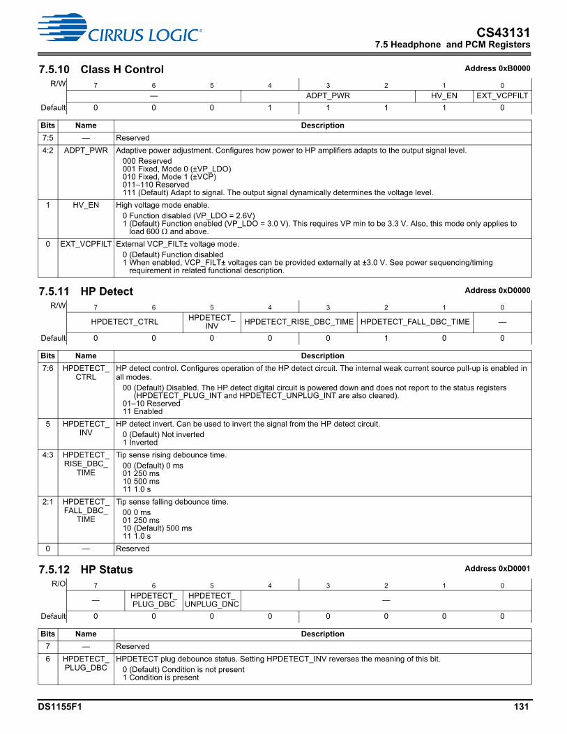
DS1155F1 131
CS431317.5 Headphone and PCM Registers
7.5.10 Class H Control Address 0xB0000
R/W 7 6 5 4 3 2 1 0
— ADPT_PWR HV_EN EXT_VCPFILT
Default 0 0 0 1 1 1 1 0
Bits Name Description
7:5 — Reserved
4:2 ADPT_PWR Adaptive power adjustment. Configures how power to HP amplifiers adapts to the output signal level.000 Reserved001 Fixed, Mode 0 (±VP_LDO)010 Fixed, Mode 1 (±VCP)011–110 Reserved111 (Default) Adapt to signal. The output signal dynamically determines the voltage level.
1 HV_EN High voltage mode enable.0 Function disabled (VP_LDO = 2.6V)1 (Default) Function enabled (VP_LDO = 3.0 V). This requires VP min to be 3.3 V. Also, this mode only applies to
load 600 and above.
0 EXT_VCPFILT External VCP_FILT± voltage mode.0 (Default) Function disabled1 When enabled, VCP_FILT± voltages can be provided externally at ±3.0 V. See power sequencing/timing
requirement in related functional description.
7.5.11 HP Detect Address 0xD0000
R/W 7 6 5 4 3 2 1 0
HPDETECT_CTRL HPDETECT_INV HPDETECT_RISE_DBC_TIME HPDETECT_FALL_DBC_TIME —
Default 0 0 0 0 0 1 0 0
Bits Name Description
7:6 HPDETECT_CTRL
HP detect control. Configures operation of the HP detect circuit. The internal weak current source pull-up is enabled in all modes.
00 (Default) Disabled. The HP detect digital circuit is powered down and does not report to the status registers (HPDETECT_PLUG_INT and HPDETECT_UNPLUG_INT are also cleared).
01–10 Reserved11 Enabled
5 HPDETECT_INV
HP detect invert. Can be used to invert the signal from the HP detect circuit.0 (Default) Not inverted1 Inverted
4:3 HPDETECT_RISE_DBC_
TIME
Tip sense rising debounce time.00 (Default) 0 ms01 250 ms10 500 ms11 1.0 s
2:1 HPDETECT_FALL_DBC_
TIME
Tip sense falling debounce time.00 0 ms01 250 ms10 (Default) 500 ms11 1.0 s
0 — Reserved
7.5.12 HP Status Address 0xD0001
R/O 7 6 5 4 3 2 1 0
— HPDETECT_PLUG_DBC
HPDETECT_UNPLUG_DNC —
Default 0 0 0 0 0 0 0 0
Bits Name Description
7 — Reserved
6 HPDETECT_PLUG_DBC
HPDETECT plug debounce status. Setting HPDETECT_INV reverses the meaning of this bit.0 (Default) Condition is not present1 Condition is present

132 DS1155F1
CS431317.5 Headphone and PCM Registers
5 HPDETECT_UNPLUG_
DBC
HPDETECT unplug debounce status. Setting HPDETECT_INV reverses the meaning of this bit.0 (Default) Condition is not present1 Condition is present
4:0 — Reserved
7.5.13 HP Load 1 Address 0xE0000
R/W 7 6 5 4 3 2 1 0
HPLOAD_EN — HPLOAD_CHN_SEL — HPLOAD_AC_
STARTHPLOAD_DC_
START
Default 0 0 0 0 0 0 0 0
Bits Name Description
7 HPLOAD_EN HP load enable.0 (Default) Function disabled1 Function enabled
6:5 — Reserved
4 HPLOAD_CHN_SEL
Select channel to perform HP load measurement.0 (Default) HPOUTA1 HPOUTB
3:2 — Reserved
1 HPLOAD_AC_START
HP load AC measurement trigger. A change from 0 to 1 initiates the measurement process. After the measurement completes, this bit must be manually changed back to 0 before initiating another process.(Default) HPLOAD_AC_START = 0
0 HPLOAD_DC_START
HP load DC measurement trigger. A change from 0 to 1 initiates the measurement process. After measurement complete, this bit must be manually changed back to 0 before initiating another process.(Default) HPLOAD_DC_START = 0
7.5.14 HP Load Measurement 1 Address 0xE0003
R/W 7 6 5 4 3 2 1 0
HPLOAD_MEAS_FREQ_LSB
Default 0 0 0 0 0 0 0 0
Bits Name Description
7:0 HPLOAD_MEAS_
FREQ_LSB
LSB of HP load measurement frequency selection for AC detect (5.86 Hz/lsb when MCLK_INT = 24.576 MHz. 5.94 Hz/lsb when MCLK_INT = 22.5792 MHz). Frequency range is 20 Hz to 20 kHz.Default: 0000 0000
7.5.15 HP Load Measurement 2 Address 0xE0004
R/W 7 6 5 4 3 2 1 0
HPLOAD_MEAS_FREQ_MSB
Default 0 0 0 0 0 0 0 0
Bits Name Description
7:0 HPLOAD_MEAS_
FREQ_MSB
MSB of HP load measurement frequency selection for AC detect (5.86 Hz/lsb when MCLK_INT = 24.576 MHz. 5.94 Hz/lsb when MCLK_INT = 22.5792 MHz). Frequency range is 20 Hz to 20 kHz.Default: 0000 0000
Bits Name Description
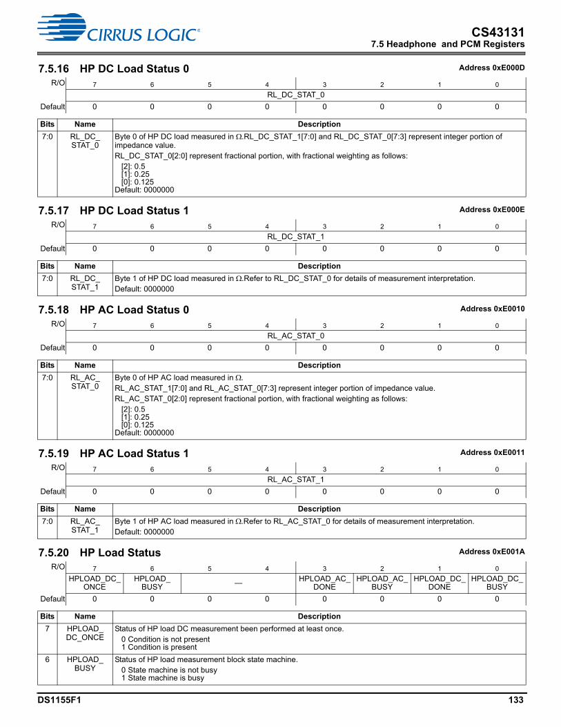
DS1155F1 133
CS431317.5 Headphone and PCM Registers
7.5.16 HP DC Load Status 0 Address 0xE000D
R/O 7 6 5 4 3 2 1 0
RL_DC_STAT_0
Default 0 0 0 0 0 0 0 0
Bits Name Description
7:0 RL_DC_STAT_0
Byte 0 of HP DC load measured in .RL_DC_STAT_1[7:0] and RL_DC_STAT_0[7:3] represent integer portion of impedance value.RL_DC_STAT_0[2:0] represent fractional portion, with fractional weighting as follows:
[2]: 0.5[1]: 0.25[0]: 0.125
Default: 0000000
7.5.17 HP DC Load Status 1 Address 0xE000E
R/O 7 6 5 4 3 2 1 0
RL_DC_STAT_1
Default 0 0 0 0 0 0 0 0
Bits Name Description
7:0 RL_DC_STAT_1
Byte 1 of HP DC load measured in .Refer to RL_DC_STAT_0 for details of measurement interpretation.Default: 0000000
7.5.18 HP AC Load Status 0 Address 0xE0010
R/O 7 6 5 4 3 2 1 0
RL_AC_STAT_0
Default 0 0 0 0 0 0 0 0
Bits Name Description
7:0 RL_AC_STAT_0
Byte 0 of HP AC load measured in .RL_AC_STAT_1[7:0] and RL_AC_STAT_0[7:3] represent integer portion of impedance value.RL_AC_STAT_0[2:0] represent fractional portion, with fractional weighting as follows:
[2]: 0.5[1]: 0.25[0]: 0.125
Default: 0000000
7.5.19 HP AC Load Status 1 Address 0xE0011
R/O 7 6 5 4 3 2 1 0
RL_AC_STAT_1
Default 0 0 0 0 0 0 0 0
Bits Name Description
7:0 RL_AC_STAT_1
Byte 1 of HP AC load measured in .Refer to RL_AC_STAT_0 for details of measurement interpretation.Default: 0000000
7.5.20 HP Load Status Address 0xE001A
R/O 7 6 5 4 3 2 1 0
HPLOAD_DC_ONCE
HPLOAD_BUSY — HPLOAD_AC_
DONEHPLOAD_AC_
BUSYHPLOAD_DC_
DONEHPLOAD_DC_
BUSY
Default 0 0 0 0 0 0 0 0
Bits Name Description
7 HPLOAD_DC_ONCE
Status of HP load DC measurement been performed at least once.0 Condition is not present1 Condition is present
6 HPLOAD_BUSY
Status of HP load measurement block state machine.0 State machine is not busy1 State machine is busy

134 DS1155F1
CS431317.6 Interrupt Status and Mask Registers
7.6 Interrupt Status and Mask Registers
5:4 — Reserved
3 HPLOAD_AC_DONE
HP load AC measurement is done status.0 Condition is not present1 Condition is present
2 HPLOAD_AC_BUSY
HP AC load measurement is “in process” status.0 Condition is not present1 Condition is present
1 HPLOAD_DC_DONE
HP load DC measurement is done status.0 Condition is not present1 Condition is present
0 HPLOAD_DC_BUSY
HP DC load measurement is “in process” status.0 Condition is not present1 Condition is present
7.6.1 Interrupt Status 1 Address 0xF0000
R/O 7 6 5 4 3 2 1 0
DAC_OVFL_INT
HPDETECT_PLUG_INT
HPDETECT_UNPLUG_INT
XTAL_READY_INT
XTAL_ERROR_INT
PLL_READY_INT
PLL_ERROR_INT
PDN_DONE_INT
Default 0 0 0 0 0 0 0 0
Bits Name Description
7 DAC_OVFL_INT
Status indicating DAC modulator overflow condition is detected.0 Condition is not present1 Condition is present
6 HPDETECT_PLUG_INT
Status indicating HP plug event is detected.0 Condition is not present1 Condition is present
5 HPDETECT_UNPLUG_INT
Status indicating HP unplug event is detected.0 Condition is not present1 Condition is present
4 XTAL_READY_INT
Status indicating XTAL is ready after PDN_XTAL is cleared.0 Condition is not present1 Condition is present
3 XTAL_ERROR_INT
Status indicating XTAL error condition is detected after PDN_XTAL is cleared.0 Condition is not present1 Condition is present
2 PLL_READY_INT
Status indicating PLL ready condition is detected after PLL_START is set.0 Condition is not present1 Condition is present
1 PLL_ERROR_INT
Status indicating PLL error condition is detected after PLL_START is set.0 Condition is not present1 Condition is present
0 PDN_DONE_INT
Status indicating PDN_HP process is completed after a request.0 Condition is not present1 Condition is present
7.6.2 Interrupt Status 2 Address 0xF0001
R/O 7 6 5 4 3 2 1 0
ASP_OVFL_INT
ASP_ERROR_INT
ASP_LATE_INT
ASP_EARLY_INT
ASP_NOLRCK_INT —
Default 0 0 0 0 0 0 0 0
Bits Name Description
7 ASP_OVFL_INT
ASP RX request overload.0 Condition is not present1 Condition is present
Bits Name Description
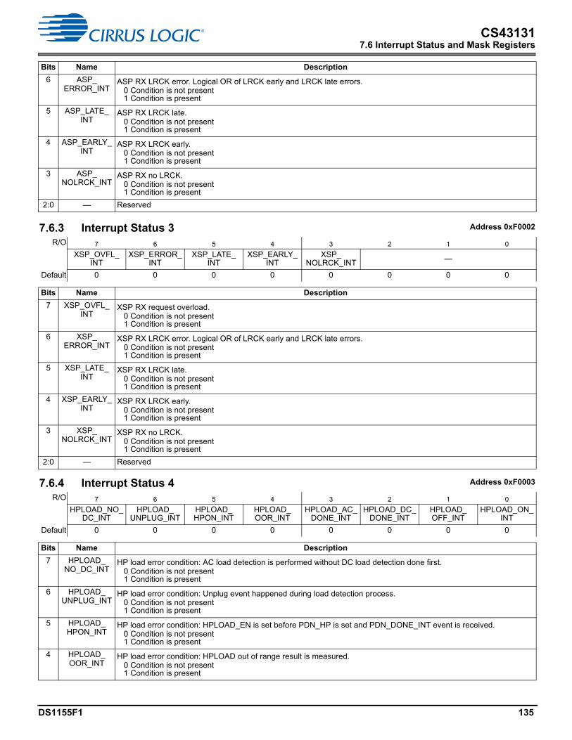
DS1155F1 135
CS431317.6 Interrupt Status and Mask Registers
6 ASP_ERROR_INT
ASP RX LRCK error. Logical OR of LRCK early and LRCK late errors.0 Condition is not present1 Condition is present
5 ASP_LATE_INT
ASP RX LRCK late.0 Condition is not present1 Condition is present
4 ASP_EARLY_INT
ASP RX LRCK early.0 Condition is not present1 Condition is present
3 ASP_NOLRCK_INT
ASP RX no LRCK.0 Condition is not present1 Condition is present
2:0 — Reserved
7.6.3 Interrupt Status 3 Address 0xF0002
R/O 7 6 5 4 3 2 1 0
XSP_OVFL_INT
XSP_ERROR_INT
XSP_LATE_INT
XSP_EARLY_INT
XSP_NOLRCK_INT —
Default 0 0 0 0 0 0 0 0
Bits Name Description
7 XSP_OVFL_INT
XSP RX request overload.0 Condition is not present1 Condition is present
6 XSP_ERROR_INT
XSP RX LRCK error. Logical OR of LRCK early and LRCK late errors.0 Condition is not present1 Condition is present
5 XSP_LATE_INT
XSP RX LRCK late.0 Condition is not present1 Condition is present
4 XSP_EARLY_INT
XSP RX LRCK early.0 Condition is not present1 Condition is present
3 XSP_NOLRCK_INT
XSP RX no LRCK.0 Condition is not present1 Condition is present
2:0 — Reserved
7.6.4 Interrupt Status 4 Address 0xF0003
R/O 7 6 5 4 3 2 1 0
HPLOAD_NO_DC_INT
HPLOAD_UNPLUG_INT
HPLOAD_HPON_INT
HPLOAD_OOR_INT
HPLOAD_AC_DONE_INT
HPLOAD_DC_DONE_INT
HPLOAD_OFF_INT
HPLOAD_ON_INT
Default 0 0 0 0 0 0 0 0
Bits Name Description
7 HPLOAD_NO_DC_INT
HP load error condition: AC load detection is performed without DC load detection done first.0 Condition is not present1 Condition is present
6 HPLOAD_UNPLUG_INT
HP load error condition: Unplug event happened during load detection process.0 Condition is not present1 Condition is present
5 HPLOAD_HPON_INT
HP load error condition: HPLOAD_EN is set before PDN_HP is set and PDN_DONE_INT event is received.0 Condition is not present1 Condition is present
4 HPLOAD_OOR_INT
HP load error condition: HPLOAD out of range result is measured.0 Condition is not present1 Condition is present
Bits Name Description
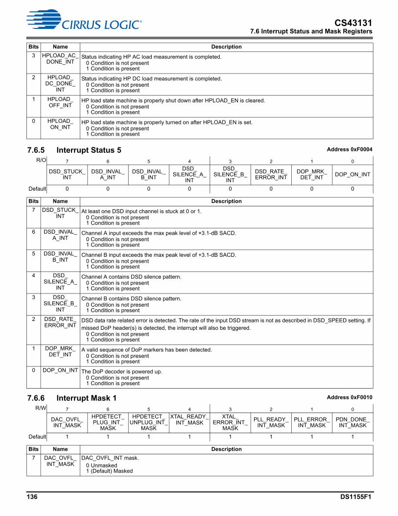
136 DS1155F1
CS431317.6 Interrupt Status and Mask Registers
3 HPLOAD_AC_DONE_INT
Status indicating HP AC load measurement is completed.0 Condition is not present1 Condition is present
2 HPLOAD_DC_DONE_
INT
Status indicating HP DC load measurement is completed.0 Condition is not present1 Condition is present
1 HPLOAD_OFF_INT
HP load state machine is properly shut down after HPLOAD_EN is cleared.0 Condition is not present1 Condition is present
0 HPLOAD_ON_INT
HP load state machine is properly turned on after HPLOAD_EN is set.0 Condition is not present1 Condition is present
7.6.5 Interrupt Status 5 Address 0xF0004
R/O 7 6 5 4 3 2 1 0
DSD_STUCK_INT
DSD_INVAL_A_INT
DSD_INVAL_B_INT
DSD_SILENCE_A_
INT
DSD_SILENCE_B_
INT
DSD_RATE_ERROR_INT
DOP_MRK_DET_INT DOP_ON_INT
Default 0 0 0 0 0 0 0 0
Bits Name Description
7 DSD_STUCK_INT
At least one DSD input channel is stuck at 0 or 1.0 Condition is not present1 Condition is present
6 DSD_INVAL_A_INT
Channel A input exceeds the max peak level of +3.1-dB SACD.0 Condition is not present1 Condition is present
5 DSD_INVAL_B_INT
Channel B input exceeds the max peak level of +3.1-dB SACD.0 Condition is not present1 Condition is present
4 DSD_SILENCE_A_
INT
Channel A contains DSD silence pattern.0 Condition is not present1 Condition is present
3 DSD_SILENCE_B_
INT
Channel B contains DSD silence pattern.0 Condition is not present1 Condition is present
2 DSD_RATE_ERROR_INT
DSD data rate related error is detected. The rate of the input DSD stream is not as described in DSD_SPEED setting. If missed DoP header(s) is detected, the interrupt will also be triggered.
0 Condition is not present1 Condition is present
1 DOP_MRK_DET_INT
A valid sequence of DoP markers has been detected.0 Condition is not present1 Condition is present
0 DOP_ON_INT The DoP decoder is powered up.0 Condition is not present1 Condition is present
7.6.6 Interrupt Mask 1 Address 0xF0010
R/W 7 6 5 4 3 2 1 0
DAC_OVFL_INT_MASK
HPDETECT_PLUG_INT_
MASK
HPDETECT_UNPLUG_INT_
MASK
XTAL_READY_INT_MASK
XTAL_ERROR_INT_
MASK
PLL_READY_INT_MASK
PLL_ERROR_INT_MASK
PDN_DONE_INT_MASK
Default 1 1 1 1 1 1 1 1
Bits Name Description
7 DAC_OVFL_INT_MASK
DAC_OVFL_INT mask.0 Unmasked1 (Default) Masked
Bits Name Description
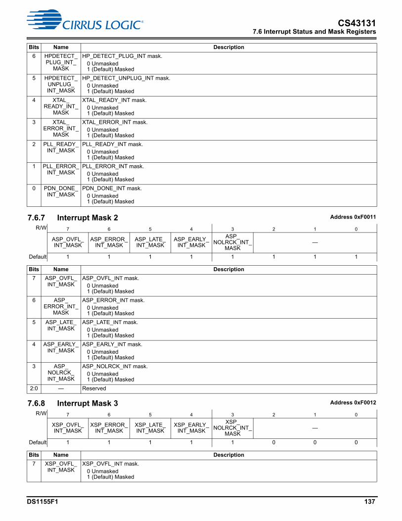
DS1155F1 137
CS431317.6 Interrupt Status and Mask Registers
6 HPDETECT_PLUG_INT_
MASK
HP_DETECT_PLUG_INT mask.0 Unmasked1 (Default) Masked
5 HPDETECT_UNPLUG_INT_MASK
HP_DETECT_UNPLUG_INT mask.0 Unmasked1 (Default) Masked
4 XTAL_READY_INT_
MASK
XTAL_READY_INT mask.0 Unmasked1 (Default) Masked
3 XTAL_ERROR_INT_
MASK
XTAL_ERROR_INT mask.0 Unmasked1 (Default) Masked
2 PLL_READY_INT_MASK
PLL_READY_INT mask.0 Unmasked1 (Default) Masked
1 PLL_ERROR_INT_MASK
PLL_ERROR_INT mask.0 Unmasked1 (Default) Masked
0 PDN_DONE_INT_MASK
PDN_DONE_INT mask.0 Unmasked1 (Default) Masked
7.6.7 Interrupt Mask 2 Address 0xF0011
R/W 7 6 5 4 3 2 1 0
ASP_OVFL_INT_MASK
ASP_ERROR_INT_MASK
ASP_LATE_INT_MASK
ASP_EARLY_INT_MASK
ASP_NOLRCK_INT_
MASK—
Default 1 1 1 1 1 1 1 1
Bits Name Description
7 ASP_OVFL_INT_MASK
ASP_OVFL_INT mask.0 Unmasked1 (Default) Masked
6 ASP_ERROR_INT_
MASK
ASP_ERROR_INT mask.0 Unmasked1 (Default) Masked
5 ASP_LATE_INT_MASK
ASP_LATE_INT mask.0 Unmasked1 (Default) Masked
4 ASP_EARLY_INT_MASK
ASP_EARLY_INT mask.0 Unmasked1 (Default) Masked
3 ASP_NOLRCK_INT_MASK
ASP_NOLRCK_INT mask.0 Unmasked1 (Default) Masked
2:0 — Reserved
7.6.8 Interrupt Mask 3 Address 0xF0012
R/W 7 6 5 4 3 2 1 0
XSP_OVFL_INT_MASK
XSP_ERROR_INT_MASK
XSP_LATE_INT_MASK
XSP_EARLY_INT_MASK
XSP_NOLRCK_INT_
MASK—
Default 1 1 1 1 1 0 0 0
Bits Name Description
7 XSP_OVFL_INT_MASK
XSP_OVFL_INT mask.0 Unmasked1 (Default) Masked
Bits Name Description
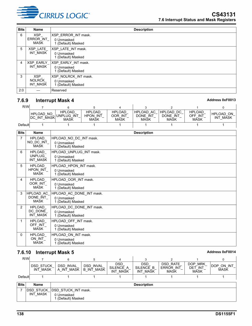
138 DS1155F1
CS431317.6 Interrupt Status and Mask Registers
6 XSP_ERROR_INT_
MASK
XSP_ERROR_INT mask.0 Unmasked1 (Default) Masked
5 XSP_LATE_INT_MASK
XSP_LATE_INT mask.0 Unmasked1 (Default) Masked
4 XSP_EARLY_INT_MASK
XSP_EARLY_INT mask.0 Unmasked1 (Default) Masked
3 XSP_NOLRCK_INT_MASK
XSP_NOLRCK_INT mask.0 Unmasked1 (Default) Masked
2:0 — Reserved
7.6.9 Interrupt Mask 4 Address 0xF0013
R/W 7 6 5 4 3 2 1 0
HPLOAD_NO_DC_INT_MASK
HPLOAD_UNPLUG_INT_
MASK
HPLOAD_HPON_INT_
MASK
HPLOAD_OOR_INT_
MASK
HPLOAD_AC_DONE_INT_
MASK
HPLOAD_DC_DONE_INT_
MASK
HPLOAD_OFF_INT_
MASK
HPLOAD_ON_INT_MASK
Default 1 1 1 1 1 1 1 1
Bits Name Description
7 HPLOAD_NO_DC_INT_
MASK
HPLOAD_NO_DC_INT mask.0 Unmasked1 (Default) Masked
6 HPLOAD_UNPLUG_INT_MASK
HPLOAD_UNPLUG_INT mask.0 Unmasked1 (Default) Masked
5 HPLOAD_HPON_INT_
MASK
HPLOAD_HPON_INT mask.0 Unmasked1 (Default) Masked
4 HPLOAD_OOR_INT_
MASK
HPLOAD_OOR_INT mask.0 Unmasked1 (Default) Masked
3 HPLOAD_AC_DONE_INT_
MASK
HPLOAD_AC_DONE_INT mask.0 Unmasked1 (Default) Masked
2 HPLOAD_DC_DONE_INT_MASK
HPLOAD_DC_DONE_INT mask.0 Unmasked1 (Default) Masked
1 HPLOAD_OFF_INT_
MASK
HPLOAD_OFF_INT mask.0 Unmasked1 (Default) Masked
0 HPLOAD_ON_INT_
MASK
HPLOAD_ON_INT mask.0 Unmasked1 (Default) Masked
7.6.10 Interrupt Mask 5 Address 0xF0014
R/W 7 6 5 4 3 2 1 0
DSD_STUCK_INT_MASK
DSD_INVAL_A_INT_MASK
DSD_INVAL_B_INT_MASK
DSD_SILENCE_A_INT_MASK
DSD_SILENCE_B_INT_MASK
DSD_RATE_ERROR_INT_
MASK
DOP_MRK_DET_INT_
MASK
DOP_ON_INT_MASK
Default 1 1 1 1 1 1 1 1
Bits Name Description
7 DSD_STUCK_INT_MASK
DSD_STUCK_INT mask.0 Unmasked1 (Default) Masked
Bits Name Description
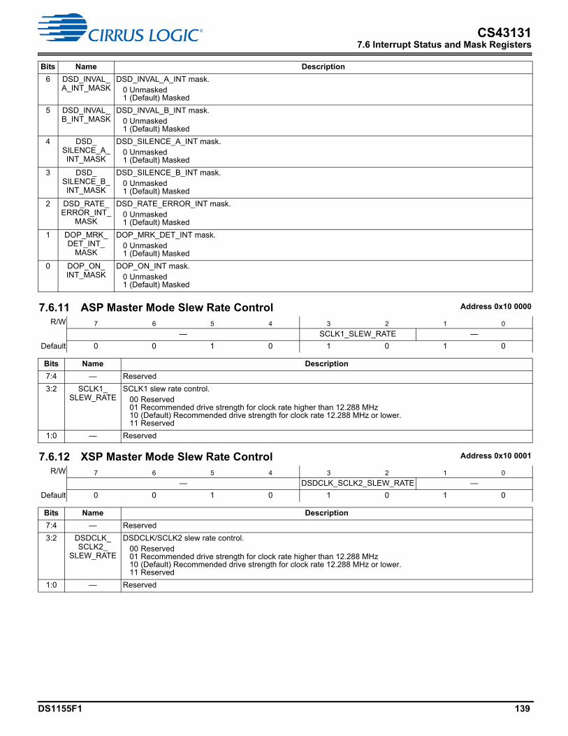
DS1155F1 139
CS431317.6 Interrupt Status and Mask Registers
6 DSD_INVAL_A_INT_MASK
DSD_INVAL_A_INT mask.0 Unmasked1 (Default) Masked
5 DSD_INVAL_B_INT_MASK
DSD_INVAL_B_INT mask.0 Unmasked1 (Default) Masked
4 DSD_SILENCE_A_INT_MASK
DSD_SILENCE_A_INT mask.0 Unmasked1 (Default) Masked
3 DSD_SILENCE_B_INT_MASK
DSD_SILENCE_B_INT mask.0 Unmasked1 (Default) Masked
2 DSD_RATE_ERROR_INT_
MASK
DSD_RATE_ERROR_INT mask.0 Unmasked1 (Default) Masked
1 DOP_MRK_DET_INT_
MASK
DOP_MRK_DET_INT mask.0 Unmasked1 (Default) Masked
0 DOP_ON_INT_MASK
DOP_ON_INT mask.0 Unmasked1 (Default) Masked
7.6.11 ASP Master Mode Slew Rate Control Address 0x10 0000
R/W 7 6 5 4 3 2 1 0
— SCLK1_SLEW_RATE —
Default 0 0 1 0 1 0 1 0
Bits Name Description
7:4 — Reserved
3:2 SCLK1_SLEW_RATE
SCLK1 slew rate control.00 Reserved01 Recommended drive strength for clock rate higher than 12.288 MHz 10 (Default) Recommended drive strength for clock rate 12.288 MHz or lower.11 Reserved
1:0 — Reserved
7.6.12 XSP Master Mode Slew Rate Control Address 0x10 0001
R/W 7 6 5 4 3 2 1 0
— DSDCLK_SCLK2_SLEW_RATE —
Default 0 0 1 0 1 0 1 0
Bits Name Description
7:4 — Reserved
3:2 DSDCLK_SCLK2_
SLEW_RATE
DSDCLK/SCLK2 slew rate control.00 Reserved01 Recommended drive strength for clock rate higher than 12.288 MHz 10 (Default) Recommended drive strength for clock rate 12.288 MHz or lower.11 Reserved
1:0 — Reserved
Bits Name Description

140 DS1155F1
CS431318 PCB Layout Considerations
8 PCB Layout Considerations
The following sections provide general guidelines for PCB layout to ensure the best performance of the CS43131.
8.1 Power Supply
As with any high-resolution converter, the CS43131 requires careful attention to power supply and grounding arrangements if its potential performance is to be realized. Fig. 2-1 shows the recommended power arrangements with VA and VCP connected to independent clean supplies. VL and VD, which power the digital circuitry, may be run from the shared system logic supply.
8.2 Grounding
Note the following:
• Extensive use of power and ground planes, ground-plane fill in unused areas, and surface-mount decoupling capacitors are recommended.
• Decoupling capacitors must be as close as possible to the CS43131 pins.
• To minimize inductance effects, the low-value ceramic capacitor must be closest to the pin and mounted on the same side of the board as the CS43131.
• To avoid unwanted coupling into the modulators, all signals, especially clocks, must be isolated from the FILT+ and FILT- pins.
• The FILT+ capacitors must be positioned to minimize the electrical path from the pin to VA.
• The FILT– capacitors must be positioned to minimize the electrical path from the pin to –VA.
• The VCP_FILT+ and VCP_FILT– capacitors must be positioned to minimize the electrical path from each respective pin to GNDCP.
8.3 HPREFA and HPREFB Routing
For best interchannel isolation performance, HPREFA and HPREFB must be routed independently to the headphone connector reference pin. The HPREFA and HPREFB are electrically connected to system’s ground plane through via at the headphone connector ground pin. Fig. 2-1 illustrates the recommended arrangements.
For interfacing the HPREFA and HPREFB pins with an IC that performs alternate pinout headset detect functions, both signals must be routed independently to the CS43131’s ground pin connecting the detected headset ground pole. Follow the recommended grounding scheme of the CS43131.
8.4 QFN Thermal Pad
The CS43131 comes in a compact QFN package, the underside of which reveals a large metal pad that serves as a thermal relief to provide maximum heat dissipation. This pad must mate with a matching copper pad on the PCB and must be electrically connected to ground. A series of vias must be used to connect this copper pad to one or more larger ground planes on other PCB layers. For best performance in split-ground systems, connect this thermal pad to GNDA.
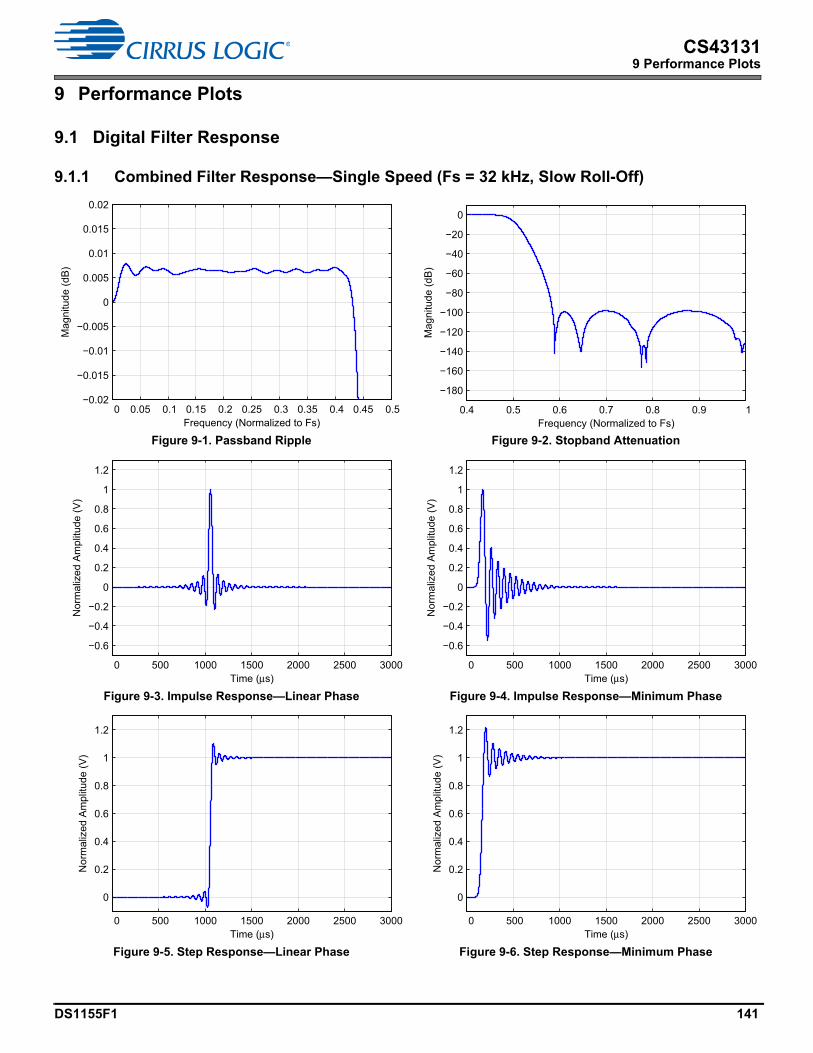
DS1155F1 141
CS431319 Performance Plots
9 Performance Plots
9.1 Digital Filter Response
9.1.1 Combined Filter Response—Single Speed (Fs = 32 kHz, Slow Roll-Off)
Figure 9-1. Passband Ripple Figure 9-2. Stopband Attenuation
Figure 9-3. Impulse Response—Linear Phase Figure 9-4. Impulse Response—Minimum Phase
Figure 9-5. Step Response—Linear Phase Figure 9-6. Step Response—Minimum Phase
0 0.05 0.1 0.15 0.2 0.25 0.3 0.35 0.4 0.45 0.5 −0.02
−0.015
−0.01
−0.005
0
0.005
0.01
0.015
0.02
Frequency (Normalized to Fs)
Mag
nitu
de (d
B)
0.4 0.5 0.6 0.7 0.8 0.9 1
−180
−160
−140
−120
−100
−80
−60
−40
−20
0
Frequency (Normalized to Fs)M
agni
tude
(dB
)
0 500 1000 1500 2000 2500 3000
−0.6
−0.4
−0.2
0
0.2
0.4
0.6
0.8
1
1.2
Time (µs)
Nor
mal
ized
Am
plitu
de (V
)
0 500 1000 1500 2000 2500 3000
−0.6
−0.4
−0.2
0
0.2
0.4
0.6
0.8
1
1.2
Time (µs)
Nor
mal
ized
Am
plitu
de (V
)
0 500 1000 1500 2000 2500 3000
0
0.2
0.4
0.6
0.8
1
1.2
Time (µs)
Nor
mal
ized
Am
plitu
de (V
)
0 500 1000 1500 2000 2500 3000
0
0.2
0.4
0.6
0.8
1
1.2
Time (µs)
Nor
mal
ized
Am
plitu
de (V
)
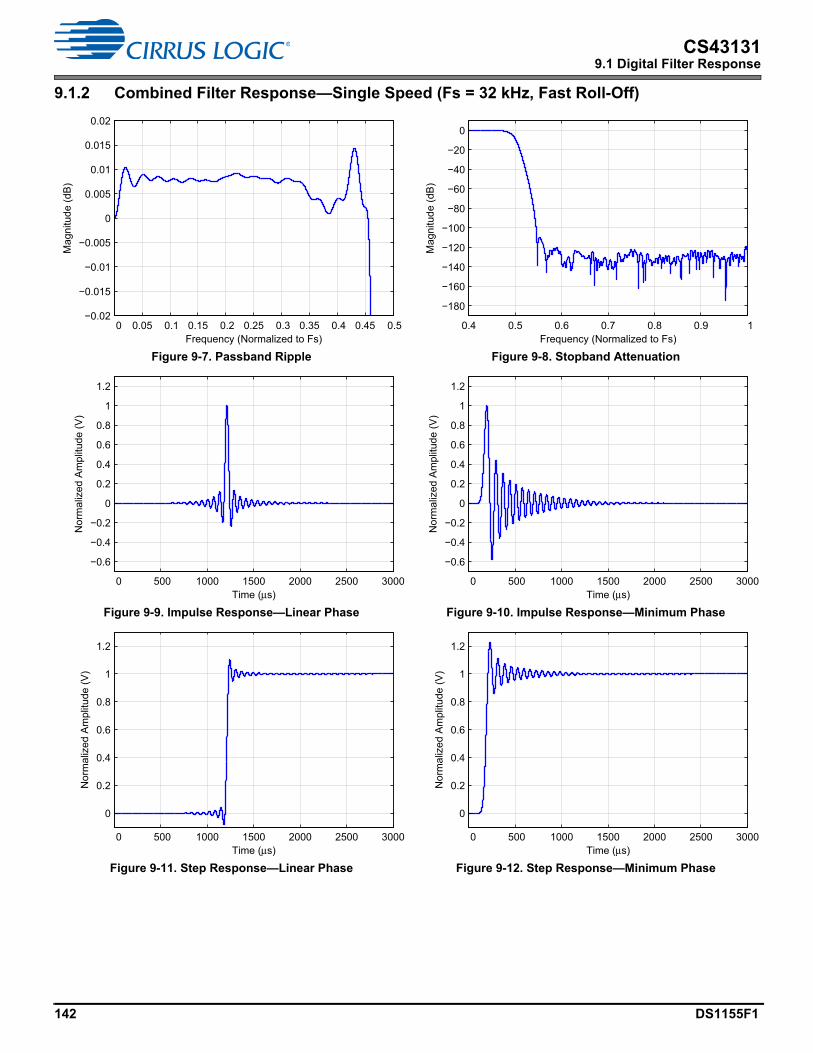
142 DS1155F1
CS431319.1 Digital Filter Response
9.1.2 Combined Filter Response—Single Speed (Fs = 32 kHz, Fast Roll-Off)
Figure 9-7. Passband Ripple Figure 9-8. Stopband Attenuation
Figure 9-9. Impulse Response—Linear Phase Figure 9-10. Impulse Response—Minimum Phase
Figure 9-11. Step Response—Linear Phase Figure 9-12. Step Response—Minimum Phase
0 0.05 0.1 0.15 0.2 0.25 0.3 0.35 0.4 0.45 0.5 −0.02
−0.015
−0.01
−0.005
0
0.005
0.01
0.015
0.02
Frequency (Normalized to Fs)
Mag
nitu
de (d
B)
0.4 0.5 0.6 0.7 0.8 0.9 1
−180
−160
−140
−120
−100
−80
−60
−40
−20
0
Frequency (Normalized to Fs)
Mag
nitu
de (d
B)
0 500 1000 1500 2000 2500 3000
−0.6
−0.4
−0.2
0
0.2
0.4
0.6
0.8
1
1.2
Time (µs)
Nor
mal
ized
Am
plitu
de (V
)
0 500 1000 1500 2000 2500 3000
−0.6
−0.4
−0.2
0
0.2
0.4
0.6
0.8
1
1.2
Time (µs)
Nor
mal
ized
Am
plitu
de (V
)
0 500 1000 1500 2000 2500 3000
0
0.2
0.4
0.6
0.8
1
1.2
Time (µs)
Nor
mal
ized
Am
plitu
de (V
)
0 500 1000 1500 2000 2500 3000
0
0.2
0.4
0.6
0.8
1
1.2
Time (µs)
Nor
mal
ized
Am
plitu
de (V
)
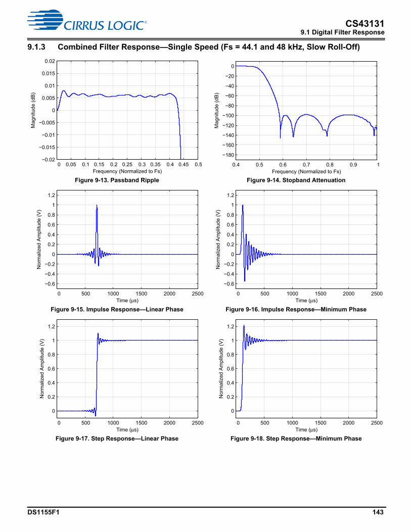
DS1155F1 143
CS431319.1 Digital Filter Response
9.1.3 Combined Filter Response—Single Speed (Fs = 44.1 and 48 kHz, Slow Roll-Off)
Figure 9-13. Passband Ripple Figure 9-14. Stopband Attenuation
Figure 9-15. Impulse Response—Linear Phase Figure 9-16. Impulse Response—Minimum Phase
Figure 9-17. Step Response—Linear Phase Figure 9-18. Step Response—Minimum Phase
0 0.05 0.1 0.15 0.2 0.25 0.3 0.35 0.4 0.45 0.5 −0.02
−0.015
−0.01
−0.005
0
0.005
0.01
0.015
0.02
Frequency (Normalized to Fs)
Mag
nitu
de (d
B)
0.4 0.5 0.6 0.7 0.8 0.9 1
−180
−160
−140
−120
−100
−80
−60
−40
−20
0
Frequency (Normalized to Fs)
Mag
nitu
de (d
B)
0 500 1000 1500 2000 2500
−0.6
−0.4
−0.2
0
0.2
0.4
0.6
0.8
1
1.2
Time (µs)
Nor
mal
ized
Am
plitu
de (V
)
0 500 1000 1500 2000 2500
−0.6
−0.4
−0.2
0
0.2
0.4
0.6
0.8
1
1.2
Time (µs)
Nor
mal
ized
Am
plitu
de (V
)
0 500 1000 1500 2000 2500
0
0.2
0.4
0.6
0.8
1
1.2
Time (µs)
Nor
mal
ized
Am
plitu
de (V
)
0 500 1000 1500 2000 2500
0
0.2
0.4
0.6
0.8
1
1.2
Time (µs)
Nor
mal
ized
Am
plitu
de (V
)
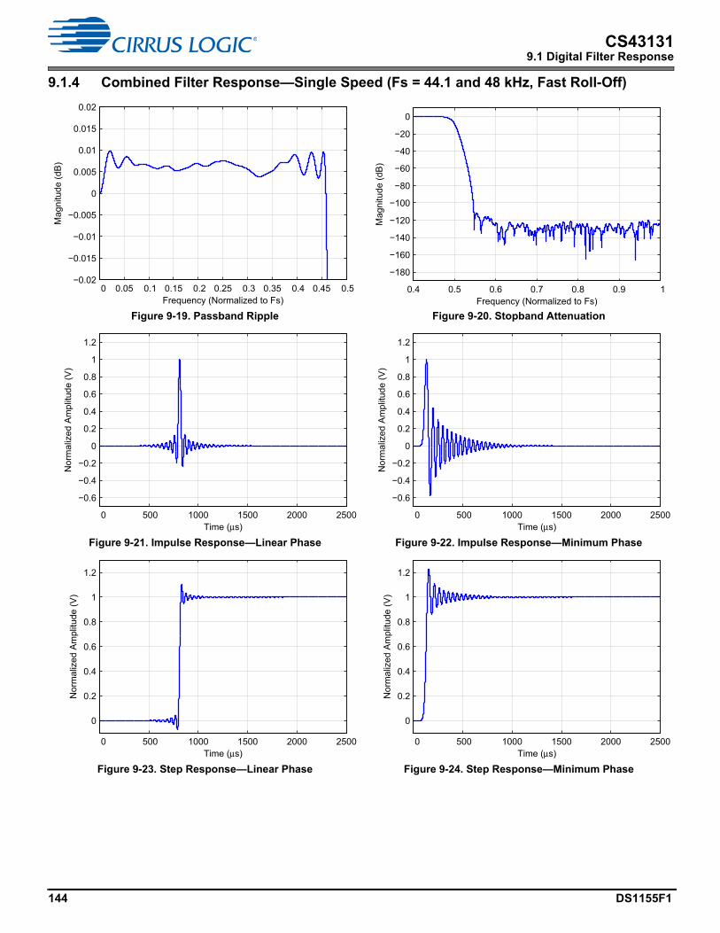
144 DS1155F1
CS431319.1 Digital Filter Response
9.1.4 Combined Filter Response—Single Speed (Fs = 44.1 and 48 kHz, Fast Roll-Off)
Figure 9-19. Passband Ripple Figure 9-20. Stopband Attenuation
Figure 9-21. Impulse Response—Linear Phase Figure 9-22. Impulse Response—Minimum Phase
Figure 9-23. Step Response—Linear Phase Figure 9-24. Step Response—Minimum Phase
0 0.05 0.1 0.15 0.2 0.25 0.3 0.35 0.4 0.45 0.5 −0.02
−0.015
−0.01
−0.005
0
0.005
0.01
0.015
0.02
Frequency (Normalized to Fs)
Mag
nitu
de (d
B)
0.4 0.5 0.6 0.7 0.8 0.9 1
−180
−160
−140
−120
−100
−80
−60
−40
−20
0
Frequency (Normalized to Fs)
Mag
nitu
de (d
B)
0 500 1000 1500 2000 2500
−0.6
−0.4
−0.2
0
0.2
0.4
0.6
0.8
1
1.2
Time (µs)
Nor
mal
ized
Am
plitu
de (V
)
0 500 1000 1500 2000 2500
−0.6
−0.4
−0.2
0
0.2
0.4
0.6
0.8
1
1.2
Time (µs)
Nor
mal
ized
Am
plitu
de (V
)
0 500 1000 1500 2000 2500
0
0.2
0.4
0.6
0.8
1
1.2
Time (µs)
Nor
mal
ized
Am
plitu
de (V
)
0 500 1000 1500 2000 2500
0
0.2
0.4
0.6
0.8
1
1.2
Time (µs)
Nor
mal
ized
Am
plitu
de (V
)
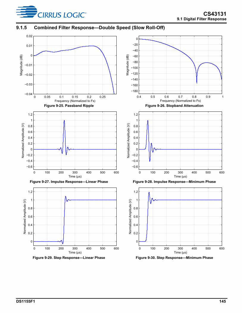
DS1155F1 145
CS431319.1 Digital Filter Response
9.1.5 Combined Filter Response—Double Speed (Slow Roll-Off)
Figure 9-25. Passband Ripple Figure 9-26. Stopband Attenuation
Figure 9-27. Impulse Response—Linear Phase Figure 9-28. Impulse Response—Minimum Phase
Figure 9-29. Step Response—Linear Phase Figure 9-30. Step Response—Minimum Phase
0 0.05 0.1 0.15 0.2 0.25−0.04
−0.03
−0.02
−0.01
0
0.01
0.02
Frequency (Normalized to Fs)
Mag
nitu
de (d
B)
0.4 0.5 0.6 0.7 0.8 0.9 1
−180
−160
−140
−120
−100
−80
−60
−40
−20
0
Frequency (Normalized to Fs)
Mag
nitu
de (d
B)
0 100 200 300 400 500 600
−0.6
−0.4
−0.2
0
0.2
0.4
0.6
0.8
1
1.2
Time (µs)
Nor
mal
ized
Am
plitu
de (V
)
0 100 200 300 400 500 600
−0.6
−0.4
−0.2
0
0.2
0.4
0.6
0.8
1
1.2
Time (µs)
Nor
mal
ized
Am
plitu
de (V
)
0 100 200 300 400 500 600
0
0.2
0.4
0.6
0.8
1
1.2
Time (µs)
Nor
mal
ized
Am
plitu
de (V
)
0 100 200 300 400 500 600
0
0.2
0.4
0.6
0.8
1
1.2
Time (µs)
Nor
mal
ized
Am
plitu
de (V
)

146 DS1155F1
CS431319.1 Digital Filter Response
9.1.6 Combined Filter Response—Double Speed (Fast Roll-Off)
Figure 9-31. Passband Ripple Figure 9-32. Stopband Attenuation
Figure 9-33. Impulse Response—Linear Phase Figure 9-34. Impulse Response—Minimum Phase
Figure 9-35. Step Response—Linear Phase Figure 9-36. Step Response—Minimum Phase
0 0.05 0.1 0.15 0.2 0.25 0.3 0.35 0.4 0.45 0.5−0.04
−0.02
0
0.02
0.04
0.06
Frequency (Normalized to Fs)
Mag
nitu
de (d
B)
0.4 0.5 0.6 0.7 0.8 0.9 1
−180
−160
−140
−120
−100
−80
−60
−40
−20
0
Frequency (Normalized to Fs)
Mag
nitu
de (d
B)
0 100 200 300 400 500 600
−0.6
−0.4
−0.2
0
0.2
0.4
0.6
0.8
1
1.2
Time (µs)
Nor
mal
ized
Am
plitu
de (V
)
0 100 200 300 400 500 600
−0.6
−0.4
−0.2
0
0.2
0.4
0.6
0.8
1
1.2
Time (µs)
Nor
mal
ized
Am
plitu
de (V
)
0 100 200 300 400 500 600
0
0.2
0.4
0.6
0.8
1
1.2
Time (µs)
Nor
mal
ized
Am
plitu
de (V
)
0 100 200 300 400 500 600
0
0.2
0.4
0.6
0.8
1
1.2
Time (µs)
Nor
mal
ized
Am
plitu
de (V
)
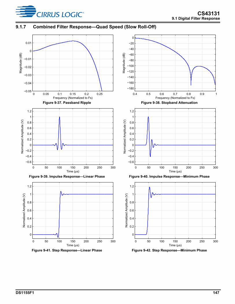
DS1155F1 147
CS431319.1 Digital Filter Response
9.1.7 Combined Filter Response—Quad Speed (Slow Roll-Off)
Figure 9-37. Passband Ripple Figure 9-38. Stopband Attenuation
Figure 9-39. Impulse Response—Linear Phase Figure 9-40. Impulse Response—Minimum Phase
Figure 9-41. Step Response—Linear Phase Figure 9-42. Step Response—Minimum Phase
0 0.05 0.1 0.15 0.2 0.25−0.05
−0.04
−0.03
−0.02
−0.01
0
0.01
Frequency (Normalized to Fs)
Mag
nitu
de (d
B)
0.4 0.5 0.6 0.7 0.8 0.9 1
−180
−160
−140
−120
−100
−80
−60
−40
−20
0
Frequency (Normalized to Fs)
Mag
nitu
de (d
B)
0 50 100 150 200 250 300
−0.6
−0.4
−0.2
0
0.2
0.4
0.6
0.8
1
1.2
Time (µs)
Nor
mal
ized
Am
plitu
de (V
)
0 50 100 150 200 250 300
−0.6
−0.4
−0.2
0
0.2
0.4
0.6
0.8
1
1.2
Time (µs)
Nor
mal
ized
Am
plitu
de (V
)
0 50 100 150 200 250 300
0
0.2
0.4
0.6
0.8
1
1.2
Time (µs)
Nor
mal
ized
Am
plitu
de (V
)
0 50 100 150 200 250 300
0
0.2
0.4
0.6
0.8
1
1.2
Time (µs)
Nor
mal
ized
Am
plitu
de (V
)

148 DS1155F1
CS431319.1 Digital Filter Response
9.1.8 Combined Filter Response—Quad Speed (Fast Roll-Off)
Figure 9-43. Passband Ripple Figure 9-44. Stopband Attenuation
Figure 9-45. Impulse Response—Linear Phase Figure 9-46. Impulse Response—Minimum Phase
Figure 9-47. Step Response—Linear Phase Figure 9-48. Step Response—Minimum Phase
0 0.05 0.1 0.15 0.2 0.25−0.05
−0.04
−0.03
−0.02
−0.01
0
0.01
0.02
0.03
Frequency (Normalized to Fs)
Mag
nitu
de (d
B)
0.4 0.5 0.6 0.7 0.8 0.9 1
−180
−160
−140
−120
−100
−80
−60
−40
−20
0
Frequency (Normalized to Fs)
Mag
nitu
de (d
B)
0 50 100 150 200 250 300
−0.6
−0.4
−0.2
0
0.2
0.4
0.6
0.8
1
1.2
Time (µs)
Nor
mal
ized
Am
plitu
de (V
)
0 50 100 150 200 250 300
−0.6
−0.4
−0.2
0
0.2
0.4
0.6
0.8
1
1.2
Time (µs)
Nor
mal
ized
Am
plitu
de (V
)
0 50 100 150 200 250 300
0
0.2
0.4
0.6
0.8
1
1.2
Time (µs)
Nor
mal
ized
Am
plitu
de (V
)
0 50 100 150 200 250 300
0
0.2
0.4
0.6
0.8
1
1.2
Time (µs)
Nor
mal
ized
Am
plitu
de (V
)
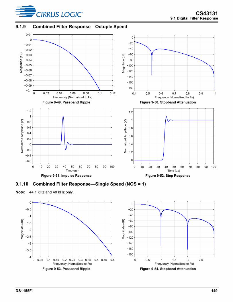
DS1155F1 149
CS431319.1 Digital Filter Response
9.1.9 Combined Filter Response—Octuple Speed
9.1.10 Combined Filter Response—Single Speed (NOS = 1)
Note: 44.1 kHz and 48 kHz only.
Figure 9-49. Passband Ripple Figure 9-50. Stopband Attenuation
Figure 9-51. Impulse Response Figure 9-52. Step Response
Figure 9-53. Passband Ripple Figure 9-54. Stopband Attenuation
0 0.02 0.04 0.06 0.08 0.1 0.12 −0.1
−0.09
−0.08
−0.07
−0.06
−0.05
−0.04
−0.03
−0.02
−0.01
0
0.01
Frequency (Normalized to Fs)
Mag
nitu
de (d
B)
0.4 0.5 0.6 0.7 0.8 0.9 1
−180
−160
−140
−120
−100
−80
−60
−40
−20
0
Frequency (Normalized to Fs)
Mag
nitu
de (d
B)
0 10 20 30 40 50 60 70 80 90 100
−0.6
−0.4
−0.2
0
0.2
0.4
0.6
0.8
1
1.2
Time (µs)
Nor
mal
ized
Am
plitu
de (V
)
0 10 20 30 40 50 60 70 80 90 100
0
0.2
0.4
0.6
0.8
1
1.2
Time (µs)
Nor
mal
ized
Am
plitu
de (V
)
0 0.05 0.1 0.15 0.2 0.25 0.3 0.35 0.4 0.45 0.5 −4
−3.5
−3
−2.5
−2
−1.5
−1
−0.5
0
Frequency (Normalized to Fs)
Mag
nitu
de (d
B)
0 0.5 1 1.5 2 2.5
−180
−160
−140
−120
−100
−80
−60
−40
−20
0
Frequency (Normalized to Fs)
Mag
nitu
de (d
B)
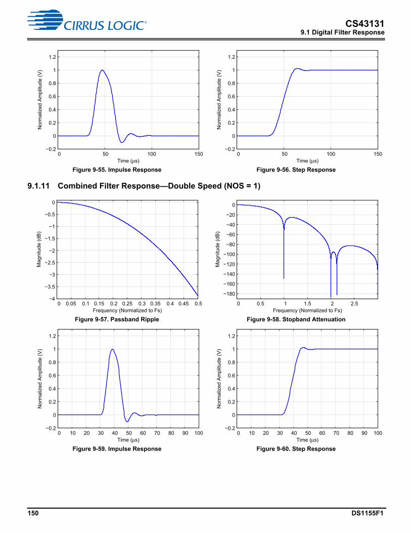
150 DS1155F1
CS431319.1 Digital Filter Response
9.1.11 Combined Filter Response—Double Speed (NOS = 1)
Figure 9-55. Impulse Response Figure 9-56. Step Response
Figure 9-57. Passband Ripple Figure 9-58. Stopband Attenuation
Figure 9-59. Impulse Response Figure 9-60. Step Response
0 50 100 150−0.2
0
0.2
0.4
0.6
0.8
1
1.2
Time (µs)
Nor
mal
ized
Am
plitu
de (V
)
0 50 100 150−0.2
0
0.2
0.4
0.6
0.8
1
1.2
Time (µs)
Nor
mal
ized
Am
plitu
de (V
)
0 0.05 0.1 0.15 0.2 0.25 0.3 0.35 0.4 0.45 0.5 −4
−3.5
−3
−2.5
−2
−1.5
−1
−0.5
0
Frequency (Normalized to Fs)
Mag
nitu
de (d
B)
0 0.5 1 1.5 2 2.5
−180
−160
−140
−120
−100
−80
−60
−40
−20
0
Frequency (Normalized to Fs)
Mag
nitu
de (d
B)
0 10 20 30 40 50 60 70 80 90 100−0.2
0
0.2
0.4
0.6
0.8
1
1.2
Time (µs)
Nor
mal
ized
Am
plitu
de (V
)
0 10 20 30 40 50 60 70 80 90 100−0.2
0
0.2
0.4
0.6
0.8
1
1.2
Time (µs)
Nor
mal
ized
Am
plitu
de (V
)
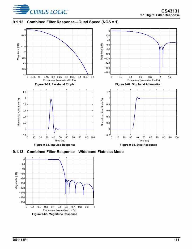
DS1155F1 151
CS431319.1 Digital Filter Response
9.1.12 Combined Filter Response—Quad Speed (NOS = 1)
9.1.13 Combined Filter Response—Wideband Flatness Mode
Figure 9-61. Passband Ripple Figure 9-62. Stopband Attenuation
Figure 9-63. Impulse Response Figure 9-64. Step Response
Figure 9-65. Magnitude Response
0 0.05 0.1 0.15 0.2 0.25 0.3 0.35 0.4 0.45 0.5 −4
−3.5
−3
−2.5
−2
−1.5
−1
−0.5
0
Frequency (Normalized to Fs)
Mag
nitu
de (d
B)
0 0.2 0.4 0.6 0.8 1 1.2
−180
−160
−140
−120
−100
−80
−60
−40
−20
0
Frequency (Normalized to Fs)
Mag
nitu
de (d
B)
0 10 20 30 40 50 60 70 80 90 100−0.2
0
0.2
0.4
0.6
0.8
1
1.2
Time (µs)
Nor
mal
ized
Am
plitu
de (V
)
0 10 20 30 40 50 60 70 80 90 100−0.2
0
0.2
0.4
0.6
0.8
1
1.2
Time (µs)
Nor
mal
ized
Am
plitu
de (V
)
0 0.1 0.2 0.3 0.4 0.5 0.6 0.7 0.8 0.9 1
−180
−160
−140
−120
−100
−80
−60
−40
−20
0
Frequency (Normalized to Fs)
Mag
nitu
de (d
B)

152 DS1155F1
CS431319.1 Digital Filter Response
9.1.14 Combined Filter Response—DSD
9.1.15 Highpass Filter and Deemphasis
Figure 9-66. Passband Ripple Figure 9-67. Stopband Attenuation
Figure 9-68. Impulse Response Figure 9-69. Step Response
Figure 9-70. Highpass Filter for PCM and DSD Paths Figure 9-71. Deemphasis
0 5 10 15 20 25 30 −0.1
−0.09
−0.08
−0.07
−0.06
−0.05
−0.04
−0.03
−0.02
−0.01
0
0.01
Frequency ( Hz)
Mag
nitu
de (d
B)
200 400 600 800 1000 1200 1400
−180
−160
−140
−120
−100
−80
−60
−40
−20
0
Frequency ( Hz)
Mag
nitu
de (d
B)
0
0 10 20 30 40 50 60 70 80 90 100
−0.2
0
0.2
0.4
0.6
0.8
1
1.2
Time (µs)
Nor
mal
ized
Am
plitu
de (V
)
0 10 20 30 40 50 60 70 80 90 100−0.2
0
0.2
0.4
0.6
0.8
1
1.2
Time (µs)
Nor
mal
ized
Am
plitu
de (V
)
0.00001 0.0001 0.001 0.01 0.1 1−30
−25
−20
−15
−10
−5
0
Frequency (Normalized to Fs)
Mag
nitu
de (d
B)
0 0.05 0.1 0.15 0.2 0.25 0.3 0.35 0.4 0.45 0.5−10
−9
−8
−7
−6
−5
−4
−3
−2
−1
0
Frequency (Normalized to Fs)
Mag
nitu
de (d
B)
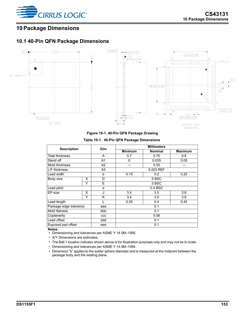
DS1155F1 153
CS4313110 Package Dimensions
10 Package Dimensions
10.1 40-Pin QFN Package Dimensions
Figure 10-1. 40-Pin QFN Package Drawing
Table 10-1. 40-Pin QFN Package Dimensions
Description DimMillimeters
Minimum Nominal MaximumTotal thickness A 0.7 0.75 0.8Stand off A1 0 0.035 0.05Mold thickness A2 — 0.55 —L/F thickness A3 0.203 REFLead width b 0.15 0.2 0.25Body size X D 5 BSC
Y E 5 BSCLead pitch e 0.4 BSCEP size X J 3.4 3.5 3.6
Y K 3.4 3.5 3.6Lead length L 0.35 0.4 0.45Package edge tolerance aaa 0.1Mold flatness bbb 0.1Coplanarity ccc 0.08Lead offset ddd 0.1Exposed pad offset eee 0.1Notes: • Dimensioning and tolerances per ASME Y 14.5M–1995. • X/Y Dimensions are estimates. • The Ball 1 location indicator shown above is for illustration purposes only and may not be to scale. • Dimensioning and tolerances per ASME Y 14.5M–1994. • Dimension “b” applies to the solder sphere diameter and is measured at the midpoint between the
package body and the seating plane.
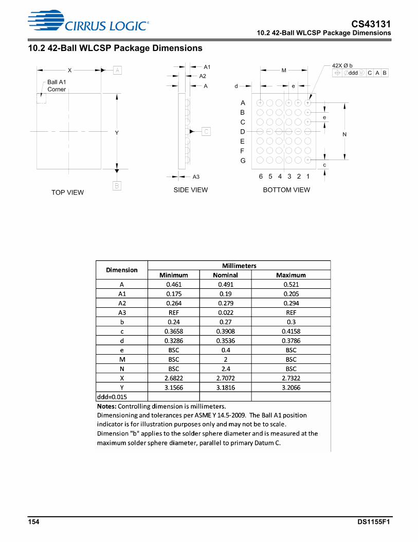
154 DS1155F1
CS4313110.2 42-Ball WLCSP Package Dimensions
10.2 42-Ball WLCSP Package Dimensions
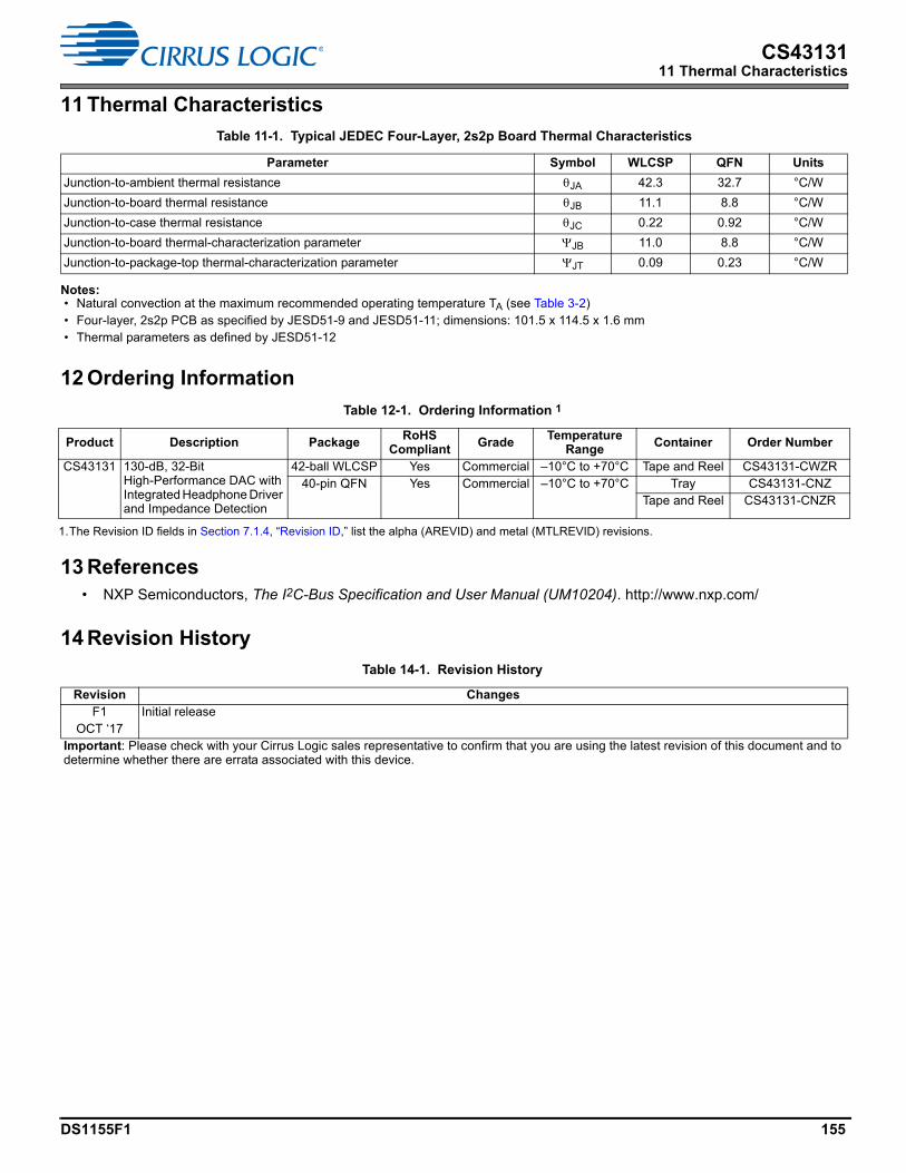
DS1155F1 155
CS4313111 Thermal Characteristics
11 Thermal Characteristics
Notes: • Natural convection at the maximum recommended operating temperature TA (see Table 3-2) • Four-layer, 2s2p PCB as specified by JESD51-9 and JESD51-11; dimensions: 101.5 x 114.5 x 1.6 mm • Thermal parameters as defined by JESD51-12
12 Ordering Information
13 References• NXP Semiconductors, The I2C-Bus Specification and User Manual (UM10204). http://www.nxp.com/
14 Revision History
Table 11-1. Typical JEDEC Four-Layer, 2s2p Board Thermal Characteristics
Parameter Symbol WLCSP QFN Units
Junction-to-ambient thermal resistance JA 42.3 32.7 °C/W
Junction-to-board thermal resistance JB 11.1 8.8 °C/W
Junction-to-case thermal resistance JC 0.22 0.92 °C/W
Junction-to-board thermal-characterization parameter JB 11.0 8.8 °C/W
Junction-to-package-top thermal-characterization parameter JT 0.09 0.23 °C/W
Table 12-1. Ordering Information 1
1.The Revision ID fields in Section 7.1.4, “Revision ID,” list the alpha (AREVID) and metal (MTLREVID) revisions.
Product Description PackageRoHS
CompliantGrade
TemperatureRange
Container Order Number
CS43131 130-dB, 32-Bit High-Performance DAC with Integrated Headphone Driver and Impedance Detection
42-ball WLCSP Yes Commercial –10°C to +70°C Tape and Reel CS43131-CWZR40-pin QFN Yes Commercial –10°C to +70°C Tray CS43131-CNZ
Tape and Reel CS43131-CNZR
Table 14-1. Revision History
Revision ChangesF1
OCT ‘17Initial release
Important: Please check with your Cirrus Logic sales representative to confirm that you are using the latest revision of this document and to determine whether there are errata associated with this device.
156 DS1155F1
CS4313114 Revision History
Contacting Cirrus Logic SupportFor all product questions and inquiries, contact a Cirrus Logic Sales Representative. To find one nearest you, go to www.cirrus.com.
IMPORTANT NOTICE
The products and services of Cirrus Logic International (UK) Limited; Cirrus Logic, Inc.; and other companies in the Cirrus Logic group (collectively either “Cirrus Logic” or “Cirrus”) are sold subject to Cirrus Logic’s terms and conditions of sale supplied at the time of order acknowledgment, including those pertaining to warranty, indemnification, and limitation of liability. Software is provided pursuant to applicable license terms. Cirrus Logic reserves the right to make changes to its products and specifications or to discontinue any product or service without notice. Customers should therefore obtain the latest version of relevant information from Cirrus Logic to verify that the information is current and complete. Testing and other quality control techniques are utilized to the extent Cirrus Logic deems necessary. Specific testing of all parameters of each device is not necessarily performed. In order to minimize risks associated with customer applications, the customer must use adequate design and operating safeguards to minimize inherent or procedural hazards. Cirrus Logic is not liable for applications assistance or customer product design. The customer is solely responsible for its selection and use of Cirrus Logic products. Use of Cirrus Logic products may entail a choice between many different modes of operation, some or all of which may require action by the user, and some or all of which may be optional. Nothing in these materials should be interpreted as instructions or suggestions to choose one mode over another. Likewise, description of a single mode should not be interpreted as a suggestion that other modes should not be used or that they would not be suitable for operation. Features and operations described herein are for illustrative purposes only.
CERTAIN APPLICATIONS USING SEMICONDUCTOR PRODUCTS MAY INVOLVE POTENTIAL RISKS OF DEATH, PERSONAL INJURY, OR SEVERE PROPERTY OR ENVIRONMENTAL DAMAGE (“CRITICAL APPLICATIONS”). CIRRUS LOGIC PRODUCTS ARE NOT DESIGNED, AUTHORIZED OR WARRANTED FOR USE IN PRODUCTS SURGICALLY IMPLANTED INTO THE BODY, AUTOMOTIVE SAFETY OR SECURITY DEVICES, NUCLEAR SYSTEMS, LIFE SUPPORT PRODUCTS OR OTHER CRITICAL APPLICATIONS. INCLUSION OF CIRRUS LOGIC PRODUCTS IN SUCH APPLICATIONS IS UNDERSTOOD TO BE FULLY AT THE CUSTOMER’S RISK AND CIRRUS LOGIC DISCLAIMS AND MAKES NO WARRANTY, EXPRESS, STATUTORY OR IMPLIED, INCLUDING THE IMPLIED WARRANTIES OF MERCHANTABILITY AND FITNESS FOR PARTICULAR PURPOSE, WITH REGARD TO ANY CIRRUS LOGIC PRODUCT THAT IS USED IN SUCH A MANNER. IF THE CUSTOMER OR CUSTOMER’S CUSTOMER USES OR PERMITS THE USE OF CIRRUS LOGIC PRODUCTS IN CRITICAL APPLICATIONS, CUSTOMER AGREES, BY SUCH USE, TO FULLY INDEMNIFY CIRRUS LOGIC, ITS OFFICERS, DIRECTORS, EMPLOYEES, DISTRIBUTORS AND OTHER AGENTS FROM ANY AND ALL LIABILITY, INCLUDING ATTORNEYS’ FEES AND COSTS, THAT MAY RESULT FROM OR ARISE IN CONNECTION WITH THESE USES.
This document is the property of Cirrus Logic and by furnishing this information, Cirrus Logic grants no license, express or implied, under any patents, mask work rights, copyrights, trademarks, trade secrets or other intellectual property rights. Any provision or publication of any third party’s products or services does not constitute Cirrus Logic’s approval, license, warranty or endorsement thereof. Cirrus Logic gives consent for copies to be made of the information contained herein only for use within your organization with respect to Cirrus Logic integrated circuits or other products of Cirrus Logic, and only if the reproduction is without alteration and is accompanied by all associated copyright, proprietary and other notices and conditions (including this notice). This consent does not extend to other copying such as copying for general distribution, advertising or promotional purposes, or for creating any work for resale. This document and its information is provided “AS IS” without warranty of any kind (express or implied). All statutory warranties and conditions are excluded to the fullest extent possible. No responsibility is assumed by Cirrus Logic for the use of information herein, including use of this information as the basis for manufacture or sale of any items, or for infringement of patents or other rights of third parties. Cirrus Logic, Cirrus, the Cirrus Logic logo design, and SoundClear are among the trademarks of Cirrus Logic. Other brand and product names may be trademarks or service marks of their respective owners.
DSD and DSD Direct Stream Digital are registered trademarks of Sony Kabushiki TA Sony Corporation.
Copyright © 2015–2017 Cirrus Logic, Inc. All rights reserved.