Embed Size (px)
Citation preview
Preliminary Product Information This document conCirrus Logic reserv
Copyright © Cirrus Log(All Rights Rese
Cirrus Logic, Inc.http://www.cirrus.com
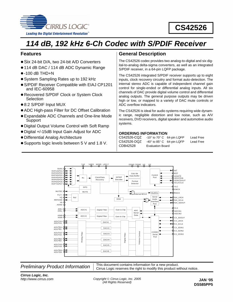
CS42526
114 dB, 192 kHz 6-Ch Codec with S/PDIF Receiver
FeaturesSix 24-bit D/A, two 24-bit A/D Converters114 dB DAC / 114 dB ADC Dynamic Range-100 dB THD+NSystem Sampling Rates up to 192 kHzS/PDIF Receiver Compatible with EIAJ CP1201 and IEC-60958
Recovered S/PDIF Clock or System Clock Selection
8:2 S/PDIF Input MUXADC High-pass Filter for DC Offset CalibrationExpandable ADC Channels and One-line Mode Support
Digital Output Volume Control with Soft RampDigital +/-15dB Input Gain Adjust for ADCDifferential Analog ArchitectureSupports logic levels between 5 V and 1.8 V.
General DescriptionThe CS42526 codec provides two analog-to-digital and six dig-ital-to-analog delta-sigma converters, as well as an integratedS/PDIF receiver, in a 64-pin LQFP package.
The CS42526 integrated S/PDIF receiver supports up to eightinputs, clock recovery circuitry and format auto-detection. Theinternal stereo ADC is capable of independent channel gaincontrol for single-ended or differential analog inputs. All sixchannels of DAC provide digital volume control and differentialanalog outputs. The general purpose outputs may be drivenhigh or low, or mapped to a variety of DAC mute controls orADC overflow indicators.
The CS42526 is ideal for audio systems requiring wide dynam-ic range, negligible distortion and low noise, such as A/Vreceivers, DVD receivers, digital speaker and automotive audiosystems.
ORDERING INFORMATIONCS42526-CQZ -10° to 70° C 64-pin LQFP Lead FreeCS42526-DQZ -40° to 85° C 64-pin LQFP Lead FreeCDB42528 Evaluation Board
RST
RXP0RXP1/GPO1
AD0/CS
SCL/CCLKSDA/CDOUTAD1/CDIN
VLC
AOUTA1+AOUTA1-
AOUTB1+
AOUTA3+AOUTA3-
AOUTA2-
AOUTB2-
AOUTA2+
AOUTB2+
AOUTB1-
AOUTB3+AOUTB3-
AINL+AINL-
AINR+AINR-
FILT+
REFGNDVQ Ref
ADC#1
ADC#2
Digital Filter
Digital Filter
Gain & Clip
Gain & Clip
CX_SCLK
CX_LRCK
CX_SDIN3
CX_SDIN2
CX_SDIN1
DGND VDLPFLTTXP
INT
Rx Clock/DataRecovery
S/PDIFDecoder
ControlPort
DAC#1
DAC#2
DAC#3
DAC#4
DAC#5
DAC#6
Dig
ital F
ilter
Vo l
u me
Co n
tro l
DGND
RXP2/GPO2RXP3/GPO3RXP4/GPO4RXP5/GPO5RXP6/GPO6RXP7/GPO7
VD
MUTEC
GPO
MUTE
Ana
log
Fil t
e r
VARX AGND
AGNDVA
CODECSerialPort
CX_SDOUT
ADCIN1ADCIN2
VLS
SAI_LRCKSAI_SCLKSAI_SDOUT
OMCK
RMCK
SerialAudio
InterfacePort
ADCSerialData
Internal MCLKMult/Div
DEM
C&U BitData Buffer
FormatDetector
tains information for a new product.es the right to modify this product without notice.
ic, Inc. 2005rved) JAN ‘05
DS585PP5
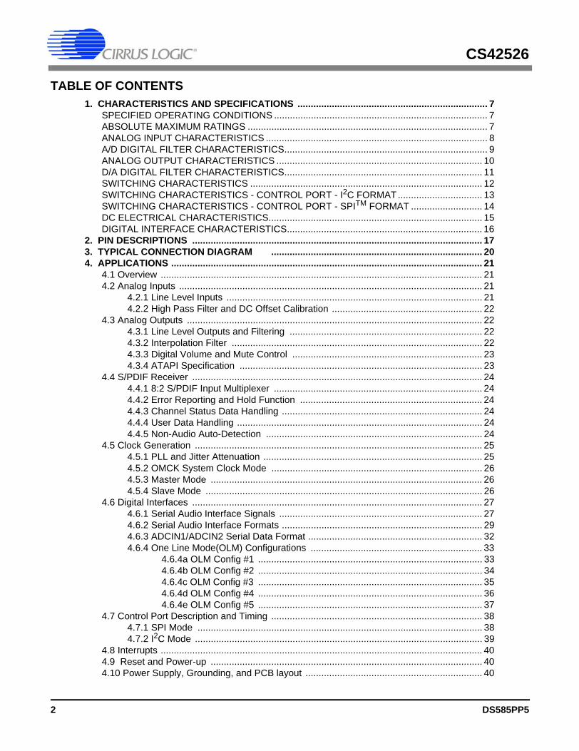
CS42526
TABLE OF CONTENTS1. CHARACTERISTICS AND SPECIFICATIONS ........................................................................ 7
SPECIFIED OPERATING CONDITIONS ................................................................................. 7ABSOLUTE MAXIMUM RATINGS ........................................................................................... 7ANALOG INPUT CHARACTERISTICS .................................................................................... 8A/D DIGITAL FILTER CHARACTERISTICS............................................................................. 9ANALOG OUTPUT CHARACTERISTICS .............................................................................. 10D/A DIGITAL FILTER CHARACTERISTICS........................................................................... 11SWITCHING CHARACTERISTICS ........................................................................................ 12SWITCHING CHARACTERISTICS - CONTROL PORT - I2C FORMAT................................ 13SWITCHING CHARACTERISTICS - CONTROL PORT - SPITM FORMAT ........................... 14DC ELECTRICAL CHARACTERISTICS................................................................................. 15DIGITAL INTERFACE CHARACTERISTICS.......................................................................... 16
2. PIN DESCRIPTIONS .............................................................................................................. 173. TYPICAL CONNECTION DIAGRAM ................................................................................ 204. APPLICATIONS ...................................................................................................................... 21
4.1 Overview .......................................................................................................................... 214.2 Analog Inputs ................................................................................................................... 21
4.2.1 Line Level Inputs ................................................................................................. 214.2.2 High Pass Filter and DC Offset Calibration ......................................................... 22
4.3 Analog Outputs ................................................................................................................ 224.3.1 Line Level Outputs and Filtering ......................................................................... 224.3.2 Interpolation Filter ............................................................................................... 224.3.3 Digital Volume and Mute Control ........................................................................ 234.3.4 ATAPI Specification ............................................................................................ 23
4.4 S/PDIF Receiver .............................................................................................................. 244.4.1 8:2 S/PDIF Input Multiplexer ............................................................................... 244.4.2 Error Reporting and Hold Function ..................................................................... 244.4.3 Channel Status Data Handling ............................................................................ 244.4.4 User Data Handling ............................................................................................. 244.4.5 Non-Audio Auto-Detection .................................................................................. 24
4.5 Clock Generation ............................................................................................................. 254.5.1 PLL and Jitter Attenuation ................................................................................... 254.5.2 OMCK System Clock Mode ................................................................................ 264.5.3 Master Mode ....................................................................................................... 264.5.4 Slave Mode ......................................................................................................... 26
4.6 Digital Interfaces .............................................................................................................. 274.6.1 Serial Audio Interface Signals ............................................................................. 274.6.2 Serial Audio Interface Formats ............................................................................ 294.6.3 ADCIN1/ADCIN2 Serial Data Format .................................................................. 324.6.4 One Line Mode(OLM) Configurations ................................................................. 33
4.6.4a OLM Config #1 ..................................................................................... 334.6.4b OLM Config #2 ..................................................................................... 344.6.4c OLM Config #3 ..................................................................................... 354.6.4d OLM Config #4 ..................................................................................... 364.6.4e OLM Config #5 ..................................................................................... 37
4.7 Control Port Description and Timing ................................................................................ 384.7.1 SPI Mode ............................................................................................................ 384.7.2 I2C Mode ............................................................................................................. 39
4.8 Interrupts .......................................................................................................................... 404.9 Reset and Power-up ....................................................................................................... 404.10 Power Supply, Grounding, and PCB layout ................................................................... 40
2 DS585PP5
CS42526
5. REGISTER QUICK REFERENCE .......................................................................................... 426. REGISTER DESCRIPTION .................................................................................................... 46
6.1 Memory Address Pointer (MAP)....................................................................................... 466.2 Chip I.D. and Revision Register (address 01h) (Read Only) ............................................ 466.3 Power Control (address 02h)............................................................................................ 476.4 Functional Mode (address 03h)........................................................................................ 486.5 Interface Formats (address 04h) ...................................................................................... 496.6 Misc Control (address 05h) .............................................................................................. 516.7 Clock Control (address 06h)............................................................................................. 526.8 OMCK/PLL_CLK Ratio (address 07h) (Read Only) ......................................................... 546.9 RVCR Status (address 08h) (Read Only)......................................................................... 546.10 Burst Preamble PC and PD Bytes (addresses 09h - 0Ch)(Read Only).......................... 556.11 Volume Transition Control (address 0Dh) ...................................................................... 566.12 Channel Mute (address 0Eh).......................................................................................... 586.13 Volume Control (addresses 0Fh, 10h, 11h, 12h, 13h, 14h) ........................................ 586.14 Channel Invert (address 17h) ......................................................................................... 586.15 Mixing Control Pair 1 (Channels A1 & B1)(address 18h)
Mixing Control Pair 2 (Channels A2 & B2)(address 19h)Mixing Control Pair 3 (Channels A3 & B3)(address 1Ah) ............................................. 59
6.16 ADC Left Channel Gain (address 1Ch) .......................................................................... 616.17 ADC Right Channel Gain (address 1Dh)........................................................................ 616.18 Receiver Mode Control (address 1Eh) ........................................................................... 616.19 Receiver Mode Control 2 (address 1Fh) ........................................................................ 626.20 Interrupt Status (address 20h) (Read Only) ................................................................... 636.21 Interrupt Mask (address 21h) ......................................................................................... 646.22 Interrupt Mode MSB (address 22h)
Interrupt Mode LSB (address 23h)................................................................................ 646.23 Channel Status Data Buffer Control (address 24h) ........................................................ 656.24 Receiver Channel Status (address 25h) (Read Only) .................................................... 666.25 Receiver Errors (address 26h) (Read Only) ................................................................... 676.26 Receiver Errors Mask (address 27h).............................................................................. 686.27 MuteC Pin Control (address 28h) ................................................................................... 686.28 RXP/General Purpose Pin Control (addresses 29h to 2Fh) ........................................... 696.29 Q-Channel Subcode Bytes 0 to 9 (addresses 30h to 39h) (Read Only)......................... 716.30 C-bit or U-bit Data Buffer (addresses 3Ah to 51h) (Read Only) ..................................... 71
7. PARAMETER DEFINITIONS .................................................................................................. 728. REFERENCES ........................................................................................................................ 739. PACKAGE DIMENSIONS ................................................................................................... 74
THERMAL CHARACTERISTICS ........................................................................................... 7410. APPENDIX A: EXTERNAL FILTERS ................................................................................... 75
10.1 ADC Input Filter ............................................................................................................. 7510.2 DAC Output Filter .......................................................................................................... 75
11. APPENDIX B: S/PDIF RECEIVER ....................................................................................... 7611.1 Error Reporting and Hold Function ................................................................................ 7611.2 Channel Status Data Handling ...................................................................................... 76
11.2.1 Channel Status Data E Buffer Access .............................................................. 7711.2.1a One Byte mode .................................................................................. 7711.2.1b Two Byte mode .................................................................................. 77
11.2.2 Serial Copy Management System (SCMS) ....................................................... 7811.3 User (U) Data E Buffer Access ...................................................................................... 78
11.3.1 Non-Audio Auto-Detection ................................................................................ 7811.3.1a Format Detection ............................................................................... 78
12. APPENDIX C: PLL FILTER .................................................................................................. 79
DS585PP5 3
CS42526
12.1 External Filter Components ........................................................................................... 8012.1.1 General ............................................................................................................. 8012.1.2 Jitter Attenuation ............................................................................................... 8012.1.3 Capacitor Selection ........................................................................................... 8112.1.4 Circuit Board Layout .......................................................................................... 81
13. APPENDIX D: EXTERNAL AES3/SPDIF/IEC60958 RECEIVER COMPONENTS .............. 8213.1 AES3 Receiver External Components ........................................................................... 82
14. APPENDIX E: ADC FILTER PLOTS .................................................................................... 8315. APPENDIX F: DAC FILTER PLOTS .................................................................................... 85
LIST OF FIGURESFigure 1. Serial Audio Port Master Mode Timing .......................................................................... 12Figure 2. Serial Audio Port Slave Mode Timing ............................................................................ 12Figure 3. Control Port Timing - I2C Format ................................................................................... 13Figure 4. Control Port Timing - SPI Format................................................................................... 14Figure 5. Typical Connection Diagram .......................................................................................... 20Figure 6. Full-Scale Analog Input .................................................................................................. 21Figure 7. Full-Scale Output ........................................................................................................... 22Figure 8. ATAPI Block Diagram (x = channel pair 1, 2, or 3) ........................................................ 23Figure 9. CS42526 Clock Generation ........................................................................................... 25Figure 10. I2S Serial Audio Formats.............................................................................................. 29Figure 11. Left Justified Serial Audio Formats .............................................................................. 30Figure 12. Right Justified Serial Audio Formats ............................................................................ 30Figure 13. One Line Mode #1 Serial Audio Format....................................................................... 31Figure 14. One Line Mode #2 Serial Audio Format....................................................................... 31Figure 15. ADCIN1/ADCIN2 Serial Audio Format ......................................................................... 32Figure 16. OLM Configuration #1 .................................................................................................. 33Figure 17. OLM Configuration #2 .................................................................................................. 34Figure 18. OLM Configuration #3 .................................................................................................. 35Figure 19. OLM Configuration #4 .................................................................................................. 36Figure 20. OLM Configuration #5 .................................................................................................. 37Figure 21. Control Port Timing in SPI Mode.................................................................................. 38Figure 22. Control Port Timing, I2C Write...................................................................................... 39Figure 23. Control Port Timing, I2C Read ..................................................................................... 39Figure 24. Recommended Analog Input Buffer ............................................................................. 75Figure 25. Recommended Analog Output Buffer .......................................................................... 75Figure 26. Channel Status Data Buffer Structure.......................................................................... 77Figure 27. PLL Block Diagram ...................................................................................................... 79Figure 28. Jitter Attenuation Characteristics of PLL ...................................................................... 80Figure 29. Recommended Layout Example .................................................................................. 81Figure 30. Consumer Input Circuit ................................................................................................ 82Figure 31. S/PDIF MUX Input Circuit ............................................................................................ 82Figure 32. TTL/CMOS Input Circuit............................................................................................... 82Figure 33. Single Speed Mode Stopband Rejection ..................................................................... 83Figure 34. Single Speed Mode Transition Band............................................................................ 83Figure 35. Single Speed Mode Transition Band (Detail) ............................................................... 83Figure 36. Single Speed Mode Passband Ripple.......................................................................... 83Figure 37. Double Speed Mode Stopband Rejection .................................................................... 83Figure 38. Double Speed Mode Transition Band .......................................................................... 83Figure 39. Double Speed Mode Transition Band (Detail).............................................................. 84Figure 40. Double Speed Mode Passband Ripple ........................................................................ 84Figure 41. Quad Speed Mode Stopband Rejection....................................................................... 84Figure 42. Quad Speed Mode Transition Band............................................................................. 84
4 DS585PP5
CS42526
Figure 43. Quad Speed Mode Transition Band (Detail) ................................................................ 84Figure 44. Quad Speed Mode Passband Ripple........................................................................... 84Figure 45. Single Speed (fast) Stopband Rejection ...................................................................... 85Figure 46. Single Speed (fast) Transition Band ............................................................................ 85Figure 47. Single Speed (fast) Transition Band (detail) ................................................................ 85Figure 48. Single Speed (fast) Passband Ripple .......................................................................... 85Figure 49. Single Speed (slow) Stopband Rejection..................................................................... 85Figure 50. Single Speed (slow) Transition Band........................................................................... 85Figure 51. Single Speed (slow) Transition Band (detail)............................................................... 86Figure 52. Single Speed (slow) Passband Ripple......................................................................... 86Figure 53. Double Speed (fast) Stopband Rejection..................................................................... 86Figure 54. Double Speed (fast) Transition Band........................................................................... 86Figure 55. Double Speed (fast) Transition Band (detail)............................................................... 86Figure 56. Double Speed (fast) Passband Ripple......................................................................... 86Figure 57. Double Speed (slow) Stopband Rejection ................................................................... 87Figure 58. Double Speed (slow) Transition Band ......................................................................... 87Figure 59. Double Speed (slow) Transition Band (detail) ............................................................. 87Figure 60. Double Speed (slow) Passband Ripple ....................................................................... 87Figure 61. Quad Speed (fast) Stopband Rejection ....................................................................... 87Figure 62. Quad Speed (fast) Transition Band ............................................................................. 87Figure 63. Quad Speed (fast) Transition Band (detail) ................................................................. 88Figure 64. Quad Speed (fast) Passband Ripple ........................................................................... 88Figure 65. Quad Speed (slow) Stopband Rejection...................................................................... 88Figure 66. Quad Speed (slow) Transition Band ............................................................................ 88Figure 67. Quad Speed (slow) Transition Band (detail) ................................................................ 88Figure 68. Quad Speed (slow) Passband Ripple .......................................................................... 88
DS585PP5 5

CS42526
LIST OF TABLESTable 1. Common OMCK Clock Frequencies ............................................................................... 26Table 2. Common PLL Output Clock Frequencies........................................................................ 26Table 3. Slave Mode Clock Ratios ................................................................................................ 26Table 4. Serial Audio Port Channel Allocations............................................................................. 27Table 5. DAC De-Emphasis .......................................................................................................... 49Table 6. Receiver De-Emphasis.................................................................................................... 49Table 7. Digital Interface Formats ................................................................................................. 50Table 8. ADC One-Line Mode ....................................................................................................... 50Table 9. DAC One-Line Mode ....................................................................................................... 50Table 10. RMCK Divider Settings.................................................................................................. 52Table 11. OMCK Frequency Settings............................................................................................ 53Table 12. Master Clock Source Select .......................................................................................... 53Table 13. AES Format Detection................................................................................................... 54Table 14. Receiver Clock Frequency Detection ............................................................................ 55Table 15. Example Digital Volume Settings .................................................................................. 58Table 16. ATAPI Decode............................................................................................................... 60Table 17. Example ADC Input Gain Settings ................................................................................ 61Table 18. TXP Output Selection.................................................................................................... 62Table 19. Receiver Input Selection ............................................................................................... 63Table 20. Auxiliary Data Width Selection ...................................................................................... 66Table 21. PLL External Component Values .................................................................................. 80Table 22. Revision History .......................................................................................................... 89
6 DS585PP5
CS42526
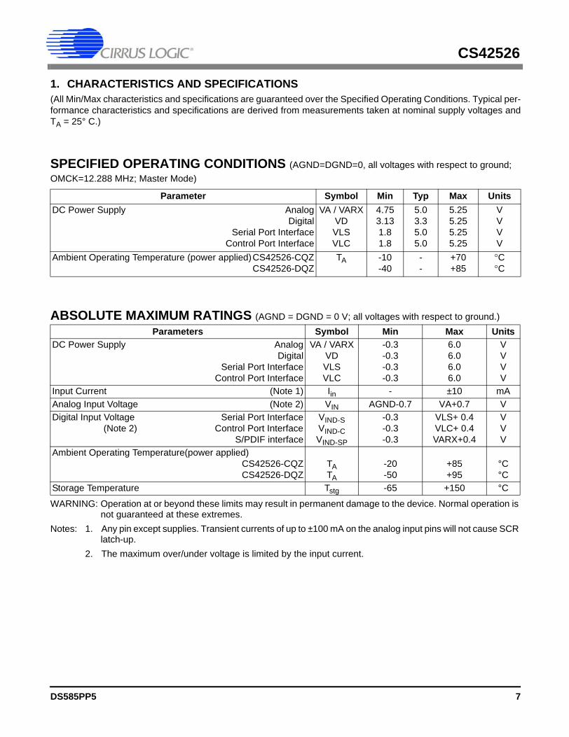
1. CHARACTERISTICS AND SPECIFICATIONS (All Min/Max characteristics and specifications are guaranteed over the Specified Operating Conditions. Typical per-formance characteristics and specifications are derived from measurements taken at nominal supply voltages andTA = 25° C.)
SPECIFIED OPERATING CONDITIONS (AGND=DGND=0, all voltages with respect to ground; OMCK=12.288 MHz; Master Mode)
ABSOLUTE MAXIMUM RATINGS (AGND = DGND = 0 V; all voltages with respect to ground.)
WARNING: Operation at or beyond these limits may result in permanent damage to the device. Normal operation is not guaranteed at these extremes.
Notes: 1. Any pin except supplies. Transient currents of up to ±100 mA on the analog input pins will not cause SCR latch-up.
2. The maximum over/under voltage is limited by the input current.
Parameter Symbol Min Typ Max UnitsDC Power Supply Analog
DigitalSerial Port Interface
Control Port Interface
VA / VARXVDVLSVLC
4.753.131.81.8
5.03.35.05.0
5.255.255.255.25
VVVV
Ambient Operating Temperature (power applied)CS42526-CQZCS42526-DQZ
TA -10-40
--
+70+85
°C°C
Parameters Symbol Min Max UnitsDC Power Supply Analog
DigitalSerial Port Interface
Control Port Interface
VA / VARXVDVLSVLC
-0.3-0.3-0.3-0.3
6.06.06.06.0
VVVV
Input Current (Note 1) Iin - ±10 mAAnalog Input Voltage (Note 2) VIN AGND-0.7 VA+0.7 VDigital Input Voltage Serial Port Interface
(Note 2) Control Port InterfaceS/PDIF interface
VIND-SVIND-CVIND-SP
-0.3-0.3-0.3
VLS+ 0.4VLC+ 0.4VARX+0.4
VVV
Ambient Operating Temperature(power applied)CS42526-CQZCS42526-DQZ
TATA
-20-50
+85+95
°C°C
Storage Temperature Tstg -65 +150 °C
DS585PP5 7
CS42526
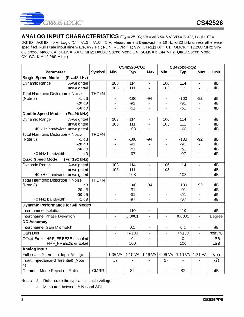
ANALOG INPUT CHARACTERISTICS (TA = 25° C; VA =VARX= 5 V, VD = 3.3 V, Logic "0" = DGND =AGND = 0 V; Logic "1" = VLS = VLC = 5 V; Measurement Bandwidth is 10 Hz to 20 kHz unless otherwise specified. Full scale input sine wave, 997 Hz.; PDN_RCVR = 1; SW_CTRL[1:0] = ‘01’; OMCK = 12.288 MHz; Sin-gle speed Mode CX_SCLK = 3.072 MHz; Double Speed Mode CX_SCLK = 6.144 MHz; Quad Speed Mode CX_SCLK = 12.288 MHz.)
Notes: 3. Referred to the typical full-scale voltage.4. Measured between AIN+ and AIN-
Parameter SymbolCS42526-CQZ
Min Typ Max CS42526-DQZ
Min Typ Max UnitSingle Speed Mode (Fs=48 kHz)Dynamic Range A-weighted
unweighted108105
114111
--
106103
114111
--
dBdB
Total Harmonic Distortion + Noise (Note 3) -1 dB
-20 dB-60 dB
THD+N---
-100-91-51
-94--
---
-100-91-51
-92--
dBdBdB
Double Speed Mode (Fs=96 kHz)Dynamic Range A-weighted
unweighted40 kHz bandwidth unweighted
108105
-
114111108
---
106103
-
114111108
---
dBdBdB
Total Harmonic Distortion + Noise (Note 3) -1 dB
-20 dB-60 dB
40 kHz bandwidth -1 dB
THD+N----
-100-91-51-97
-94---
----
-100-91-51-97
-92---
dBdBdBdB
Quad Speed Mode (Fs=192 kHz)Dynamic Range A-weighted
unweighted40 kHz bandwidth unweighted
108105
-
114111108
---
106103
-
114111108
---
dBdBdB
Total Harmonic Distortion + Noise(Note 3) -1 dB
-20 dB-60 dB
40 kHz bandwidth -1 dB
THD+N----
-100-91-51-97
-94---
----
-100-91-51-97
-92---
dBdBdBdB
Dynamic Performance for All ModesInterchannel Isolation - 110 - - 110 - dBInterchannel Phase Deviation - 0.0001 - - 0.0001 - DegreeDC AccuracyInterchannel Gain Mismatch - 0.1 - - 0.1 - dBGain Drift - +/-100 - - +/-100 - ppm/°COffset Error HPF_FREEZE disabled
HPF_FREEZE enabled--
0100
--
--
0100
--
LSBLSB
Analog InputFull-scale Differential Input Voltage 1.05 VA 1.10 VA 1.16 VA 0.99 VA 1.10 VA 1.21 VA VppInput Impedance(differential) (Note 4)
17 - - 17 - - kΩ
Common Mode Rejection Ratio CMRR - 82 - - 82 - dB
8 DS585PP5
CS42526
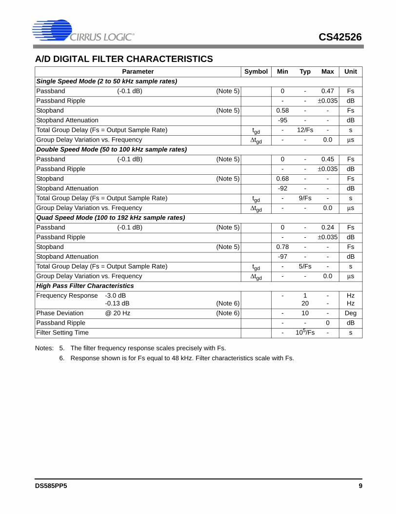
A/D DIGITAL FILTER CHARACTERISTICS
Notes: 5. The filter frequency response scales precisely with Fs.6. Response shown is for Fs equal to 48 kHz. Filter characteristics scale with Fs.
Parameter Symbol Min Typ Max UnitSingle Speed Mode (2 to 50 kHz sample rates)Passband (-0.1 dB) (Note 5) 0 - 0.47 FsPassband Ripple - - ±0.035 dBStopband (Note 5) 0.58 - - FsStopband Attenuation -95 - - dBTotal Group Delay (Fs = Output Sample Rate) tgd - 12/Fs - sGroup Delay Variation vs. Frequency ∆tgd - - 0.0 µsDouble Speed Mode (50 to 100 kHz sample rates)Passband (-0.1 dB) (Note 5) 0 - 0.45 FsPassband Ripple - - ±0.035 dBStopband (Note 5) 0.68 - - FsStopband Attenuation -92 - - dBTotal Group Delay (Fs = Output Sample Rate) tgd - 9/Fs - sGroup Delay Variation vs. Frequency ∆tgd - - 0.0 µsQuad Speed Mode (100 to 192 kHz sample rates)Passband (-0.1 dB) (Note 5) 0 - 0.24 FsPassband Ripple - - ±0.035 dBStopband (Note 5) 0.78 - - FsStopband Attenuation -97 - - dBTotal Group Delay (Fs = Output Sample Rate) tgd - 5/Fs - sGroup Delay Variation vs. Frequency ∆tgd - - 0.0 µsHigh Pass Filter CharacteristicsFrequency Response -3.0 dB
-0.13 dB (Note 6)- 1
20--
HzHz
Phase Deviation @ 20 Hz (Note 6) - 10 - DegPassband Ripple - - 0 dBFilter Setting Time - 105/Fs - s
DS585PP5 9
CS42526
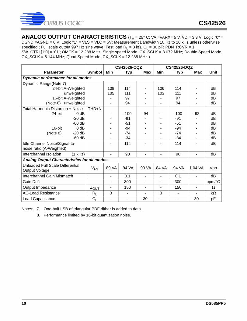
ANALOG OUTPUT CHARACTERISTICS (TA = 25° C; VA =VARX= 5 V, VD = 3.3 V, Logic "0" = DGND =AGND = 0 V; Logic "1" = VLS = VLC = 5V; Measurement Bandwidth 10 Hz to 20 kHz unless otherwise specified.; Full scale output 997 Hz sine wave, Test load RL = 3 kΩ, CL = 30 pF; PDN_RCVR = 1; SW_CTRL[1:0] = ‘01’; OMCK = 12.288 MHz; Single speed Mode, CX_SCLK = 3.072 MHz; Double Speed Mode, CX_SCLK = 6.144 MHz; Quad Speed Mode, CX_SCLK = 12.288 MHz.)
Notes: 7. One-half LSB of triangular PDF dither is added to data.8. Performance limited by 16-bit quantization noise.
Parameter SymbolCS42526-CQZ
Min Typ Max CS42526-DQZ
Min Typ Max UnitDynamic performance for all modesDynamic Range(Note 7)
24-bit A-Weightedunweighted
16-bit A-Weighted(Note 8) unweighted
108105
--
1141119794
----
106103
--
1141119794
----
dBdBdBdB
Total Harmonic Distortion + Noise24-bit 0 dB
-20 dB-60 dB
16-bit 0 dB(Note 8) -20 dB
-60 dB
THD+N------
-100-91-51-94-74-34
-94----
------
-100-91-51-94-74-34
-92-----
dBdBdBdBdBdB
Idle Channel Noise/Signal-to-noise ratio (A-Weighted)
- 114 - - 114 - dB
Interchannel Isolation (1 kHz) - 90 - - 90 - dBAnalog Output Characteristics for all modesUnloaded Full Scale Differential Output Voltage VFS .89 VA .94 VA .99 VA .84 VA .94 VA 1.04 VA Vpp
Interchannel Gain Mismatch - 0.1 - - 0.1 - dBGain Drift - 300 - - 300 - ppm/°COutput Impedance ZOUT - 150 - - 150 - ΩAC-Load Resistance RL 3 - - 3 - - kΩLoad Capacitance CL - - 30 - - 30 pF
10 DS585PP5
CS42526
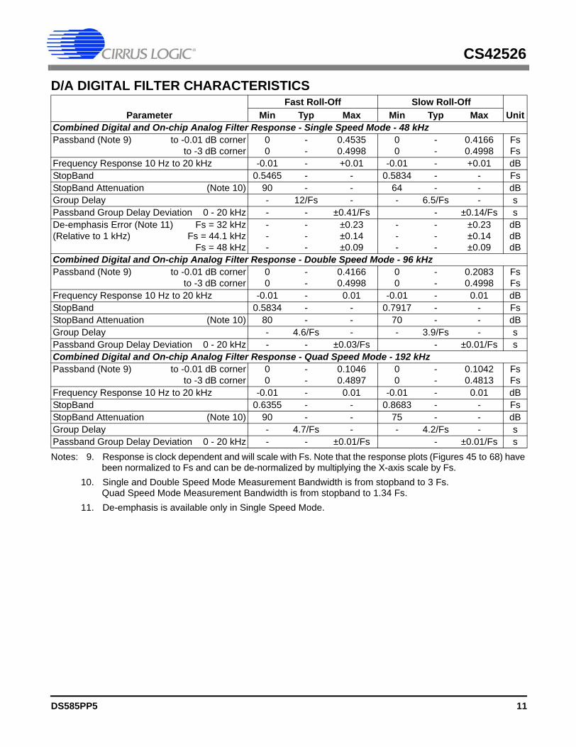
D/A DIGITAL FILTER CHARACTERISTICS
Notes: 9. Response is clock dependent and will scale with Fs. Note that the response plots (Figures 45 to 68) have been normalized to Fs and can be de-normalized by multiplying the X-axis scale by Fs.
10. Single and Double Speed Mode Measurement Bandwidth is from stopband to 3 Fs. Quad Speed Mode Measurement Bandwidth is from stopband to 1.34 Fs.
11. De-emphasis is available only in Single Speed Mode.
ParameterFast Roll-Off Slow Roll-Off
UnitMin Typ Max Min Typ MaxCombined Digital and On-chip Analog Filter Response - Single Speed Mode - 48 kHz Passband (Note 9) to -0.01 dB corner
to -3 dB corner00
--
0.45350.4998
00
--
0.41660.4998
FsFs
Frequency Response 10 Hz to 20 kHz -0.01 - +0.01 -0.01 - +0.01 dBStopBand 0.5465 - - 0.5834 - - FsStopBand Attenuation (Note 10) 90 - - 64 - - dBGroup Delay - 12/Fs - - 6.5/Fs - sPassband Group Delay Deviation 0 - 20 kHz - - ±0.41/Fs - ±0.14/Fs sDe-emphasis Error (Note 11) Fs = 32 kHz(Relative to 1 kHz) Fs = 44.1 kHz
Fs = 48 kHz
---
---
±0.23±0.14±0.09
---
---
±0.23±0.14±0.09
dBdBdB
Combined Digital and On-chip Analog Filter Response - Double Speed Mode - 96 kHzPassband (Note 9) to -0.01 dB corner
to -3 dB corner00
--
0.41660.4998
00
--
0.20830.4998
FsFs
Frequency Response 10 Hz to 20 kHz -0.01 - 0.01 -0.01 - 0.01 dBStopBand 0.5834 - - 0.7917 - - FsStopBand Attenuation (Note 10) 80 - - 70 - - dBGroup Delay - 4.6/Fs - - 3.9/Fs - sPassband Group Delay Deviation 0 - 20 kHz - - ±0.03/Fs - ±0.01/Fs sCombined Digital and On-chip Analog Filter Response - Quad Speed Mode - 192 kHz Passband (Note 9) to -0.01 dB corner
to -3 dB corner00
--
0.10460.4897
00
--
0.10420.4813
FsFs
Frequency Response 10 Hz to 20 kHz -0.01 - 0.01 -0.01 - 0.01 dBStopBand 0.6355 - - 0.8683 - - FsStopBand Attenuation (Note 10) 90 - - 75 - - dBGroup Delay - 4.7/Fs - - 4.2/Fs - sPassband Group Delay Deviation 0 - 20 kHz - - ±0.01/Fs - ±0.01/Fs s
DS585PP5 11
CS42526
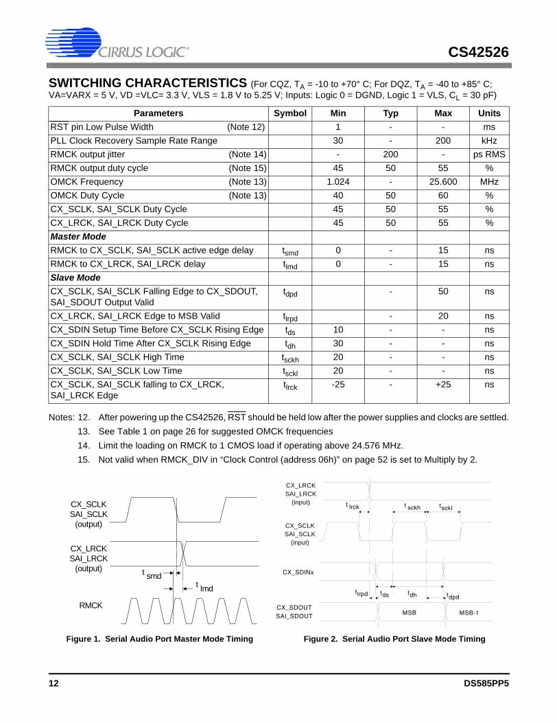
SWITCHING CHARACTERISTICS (For CQZ, TA = -10 to +70° C; For DQZ, TA = -40 to +85° C; VA=VARX = 5 V, VD =VLC= 3.3 V, VLS = 1.8 V to 5.25 V; Inputs: Logic 0 = DGND, Logic 1 = VLS, CL = 30 pF)
Notes: 12. After powering up the CS42526, RST should be held low after the power supplies and clocks are settled.13. See Table 1 on page 26 for suggested OMCK frequencies14. Limit the loading on RMCK to 1 CMOS load if operating above 24.576 MHz. 15. Not valid when RMCK_DIV in “Clock Control (address 06h)” on page 52 is set to Multiply by 2.
Parameters Symbol Min Typ Max UnitsRST pin Low Pulse Width (Note 12) 1 - - msPLL Clock Recovery Sample Rate Range 30 - 200 kHzRMCK output jitter (Note 14) - 200 - ps RMSRMCK output duty cycle (Note 15) 45 50 55 %OMCK Frequency (Note 13) 1.024 - 25.600 MHzOMCK Duty Cycle (Note 13) 40 50 60 %CX_SCLK, SAI_SCLK Duty Cycle 45 50 55 %CX_LRCK, SAI_LRCK Duty Cycle 45 50 55 %Master ModeRMCK to CX_SCLK, SAI_SCLK active edge delay tsmd 0 - 15 nsRMCK to CX_LRCK, SAI_LRCK delay tlmd 0 - 15 nsSlave ModeCX_SCLK, SAI_SCLK Falling Edge to CX_SDOUT, SAI_SDOUT Output Valid
tdpd - 50 ns
CX_LRCK, SAI_LRCK Edge to MSB Valid tlrpd - 20 nsCX_SDIN Setup Time Before CX_SCLK Rising Edge tds 10 - - nsCX_SDIN Hold Time After CX_SCLK Rising Edge tdh 30 - - nsCX_SCLK, SAI_SCLK High Time tsckh 20 - - nsCX_SCLK, SAI_SCLK Low Time tsckl 20 - - nsCX_SCLK, SAI_SCLK falling to CX_LRCK, SAI_LRCK Edge
tlrck -25 - +25 ns
CX_SCLKSAI_SCLK
(output)
RMCK
t smdt lmd
CX_LRCKSAI_LRCK
(output)
sckh sckltt
MSB MSB-1
tdpd
CX_SDOUTSAI_SDOUT
CX_SDINx
dhtdstlrpdt
lrckt
CX_SCLKSAI_SCLK
(input)
CX_LRCKSAI_LRCK
(input)
Figure 1. Serial Audio Port Master Mode Timing Figure 2. Serial Audio Port Slave Mode Timing
12 DS585PP5
CS42526
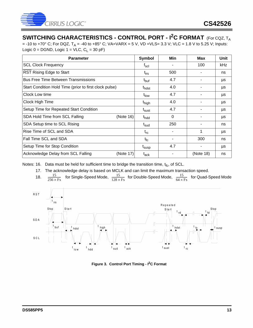
SWITCHING CHARACTERISTICS - CONTROL PORT - I2C FORMAT (For CQZ, TA = -10 to +70° C; For DQZ, TA = -40 to +85° C; VA=VARX = 5 V, VD =VLS= 3.3 V; VLC = 1.8 V to 5.25 V; Inputs: Logic 0 = DGND, Logic 1 = VLC, CL = 30 pF)
Notes: 16. Data must be held for sufficient time to bridge the transition time, tfc, of SCL.17. The acknowledge delay is based on MCLK and can limit the maximum transaction speed.18. for Single-Speed Mode, for Double-Speed Mode, for Quad-Speed Mode
Parameter Symbol Min Max UnitSCL Clock Frequency fscl - 100 kHz
RST Rising Edge to Start tirs 500 - ns
Bus Free Time Between Transmissions tbuf 4.7 - µs
Start Condition Hold Time (prior to first clock pulse) thdst 4.0 - µs
Clock Low time tlow 4.7 - µs
Clock High Time thigh 4.0 - µs
Setup Time for Repeated Start Condition tsust 4.7 - µs
SDA Hold Time from SCL Falling (Note 16) thdd 0 - µs
SDA Setup time to SCL Rising tsud 250 - ns
Rise Time of SCL and SDA trc - 1 µs
Fall Time SCL and SDA tfc - 300 ns
Setup Time for Stop Condition tsusp 4.7 - µs
Acknowledge Delay from SCL Falling (Note 17) tack - (Note 18) ns
15256 Fs×--------------------- 15
128 Fs×--------------------- 15
64 Fs×------------------
t bu f t hdst
tl o w
thdd
t h igh
t sud
S top S t a r t
S D A
S C L
t irs
R S T
thdst
t rc
t fc
t sust
t susp
S ta r t S topR e p e a te d
t rd t fd
t ack
Figure 3. Control Port Timing - I2C Format
DS585PP5 13
CS42526
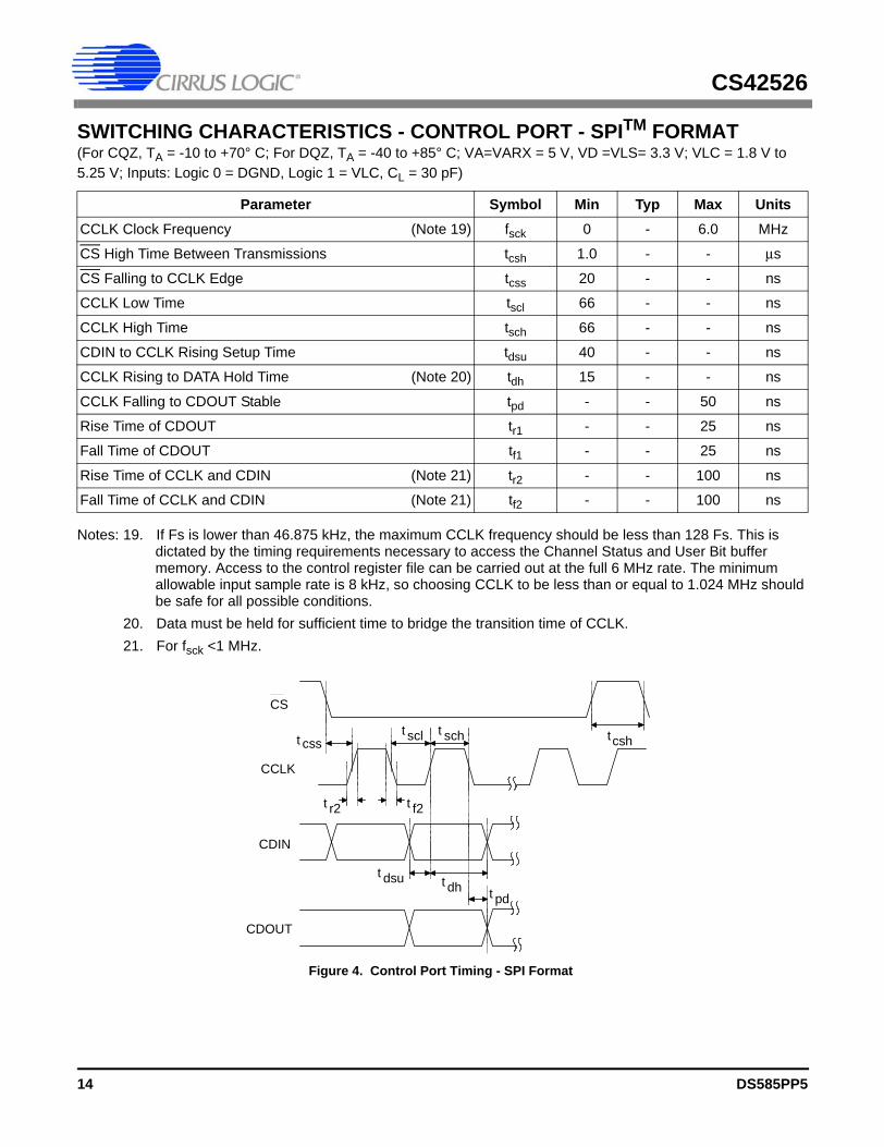
SWITCHING CHARACTERISTICS - CONTROL PORT - SPITM FORMAT (For CQZ, TA = -10 to +70° C; For DQZ, TA = -40 to +85° C; VA=VARX = 5 V, VD =VLS= 3.3 V; VLC = 1.8 V to 5.25 V; Inputs: Logic 0 = DGND, Logic 1 = VLC, CL = 30 pF)
Notes: 19. If Fs is lower than 46.875 kHz, the maximum CCLK frequency should be less than 128 Fs. This is dictated by the timing requirements necessary to access the Channel Status and User Bit buffer memory. Access to the control register file can be carried out at the full 6 MHz rate. The minimum allowable input sample rate is 8 kHz, so choosing CCLK to be less than or equal to 1.024 MHz should be safe for all possible conditions.
20. Data must be held for sufficient time to bridge the transition time of CCLK.21. For fsck <1 MHz.
Parameter Symbol Min Typ Max UnitsCCLK Clock Frequency (Note 19) fsck 0 - 6.0 MHz
CS High Time Between Transmissions tcsh 1.0 - - µs
CS Falling to CCLK Edge tcss 20 - - ns
CCLK Low Time tscl 66 - - ns
CCLK High Time tsch 66 - - ns
CDIN to CCLK Rising Setup Time tdsu 40 - - ns
CCLK Rising to DATA Hold Time (Note 20) tdh 15 - - ns
CCLK Falling to CDOUT Stable tpd - - 50 ns
Rise Time of CDOUT tr1 - - 25 ns
Fall Time of CDOUT tf1 - - 25 ns
Rise Time of CCLK and CDIN (Note 21) tr2 - - 100 ns
Fall Time of CCLK and CDIN (Note 21) tf2 - - 100 ns
t r2 t f2
t dsu t dh
t scht scl
CS
CCLK
CDIN
t css
t pd
CDOUT
tcsh
Figure 4. Control Port Timing - SPI Format
14 DS585PP5
CS42526
DC ELECTRICAL CHARACTERISTICS (TA = 25° C; AGND=DGND=0, all voltages with respect to ground; OMCK=12.288 MHz; Master Mode)
Notes: 22. Current consumption increases with increasing FS and increasing OMCK. Max values are based on highest FS and highest OMCK. Variance between speed modes is negligible.
23. ILC measured with no external loading on the SDA pin.24. Power down mode is defined as RST pin = Low with all clock and data lines held static. 25. Valid with the recommended capacitor values on FILT+ and VQ as shown in Figure 5.
Parameter Symbol Min Typ Max UnitsPower Supply Current normal operation, VA = VARX = 5 V(Note 22) VD = 5 V
VD = 3.3 VInterface current, VLC=5 V (Note 23)
VLS=5 Vpower-down state (all supplies) (Note 24)
IAIDIDILCILSIpd
------
758551
25013
250
------
mAmAmAµAmAµA
Power Consumption (Note 22)VA=VARX=5 V, VD=VLS=VLC=3.3 V normal operation
power-down (Note 24)VA=VARX=5 V, VD=VLS=VLC=5 V normal operation
power-down (Note 24)
----
5871.258661.25
650-
960-
mWmWmWmW
Power Supply Rejection Ratio (Note 25) (1 kHz)(60 Hz)
PSRR --
6040
--
dBdB
VQ Nominal VoltageVQ Output ImpedanceVQ Maximum allowable DC current
---
2.750
0.01
---
VkΩmA
FILT+ Nominal VoltageFILT+ Output ImpedanceFILT+ Maximum allowable DC current
---
5.035
0.01
---
VkΩmA
DS585PP5 15
CS42526
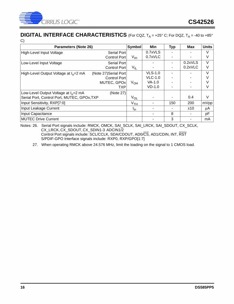
DIGITAL INTERFACE CHARACTERISTICS (For CQZ, TA = +25° C; For DQZ, TA = -40 to +85° C)
Notes: 26. Serial Port signals include: RMCK, OMCK, SAI_SCLK, SAI_LRCK, SAI_SDOUT, CX_SCLK, CX_LRCK, CX_SDOUT, CX_SDIN1-3 ADCIN1/2 Control Port signals include: SCL/CCLK, SDA/CDOUT, AD0/CS, AD1/CDIN, INT, RST S/PDIF-GPO Interface signals include: RXP0, RXP/GPO[1:7]
27. When operating RMCK above 24.576 MHz, limit the loading on the signal to 1 CMOS load.
Parameters (Note 26) Symbol Min Typ Max UnitsHigh-Level Input Voltage Serial Port
Control Port VIH
0.7xVLS0.7xVLC
--
--
VV
Low-Level Input Voltage Serial PortControl Port VIL
--
--
0.2xVLS0.2xVLC
VV
High-Level Output Voltage at Io=2 mA (Note 27)Serial PortControl Port
MUTEC, GPOxTXP
VOH
VLS-1.0VLC-1.0VA-1.0VD-1.0
----
----
VVVV
Low-Level Output Voltage at Io=2 mA (Note 27)Serial Port, Control Port, MUTEC, GPOx,TXP VOL - - 0.4 VInput Sensitivity, RXP[7:0] VTH - 150 200 mVppInput Leakage Current Iin - - ±10 µAInput Capacitance - 8 - pFMUTEC Drive Current - 3 - mA
16 DS585PP5
CS42526
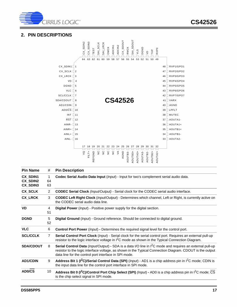
2. PIN DESCRIPTIONS
Pin Name # Pin DescriptionCX_SDIN1CX_SDIN2CX_SDIN3
16463
Codec Serial Audio Data Input (Input) - Input for two’s complement serial audio data.
CX_SCLK 2 CODEC Serial Clock (Input/Output) - Serial clock for the CODEC serial audio interface.
CX_LRCK 3 CODEC Left Right Clock (Input/Output) - Determines which channel, Left or Right, is currently active on the CODEC serial audio data line.
VD 451
Digital Power (Input) - Positive power supply for the digital section.
DGND 552
Digital Ground (Input) - Ground reference. Should be connected to digital ground.
VLC 6 Control Port Power (Input) - Determines the required signal level for the control port.
SCL/CCLK 7 Serial Control Port Clock (Input) - Serial clock for the serial control port. Requires an external pull-up resistor to the logic interface voltage in I2C mode as shown in the Typical Connection Diagram.
SDA/CDOUT 8 Serial Control Data (Input/Output) - SDA is a data I/O line in I2C mode and requires an external pull-up resistor to the logic interface voltage, as shown in the Typical Connection Diagram. CDOUT is the output data line for the control port interface in SPI mode.
AD1/CDIN 9 Address Bit 1 (I2C)/Serial Control Data (SPI) (Input) - AD1 is a chip address pin in I2C mode; CDIN is the input data line for the control port interface in SPI mode.
AD0/CS 10 Address Bit 0 (I2C)/Control Port Chip Select (SPI) (Input) - AD0 is a chip address pin in I2C mode; CS is the chip select signal in SPI mode.
1
2
3
4
5
6
7
8
9
10
11
12
13
14
15
16
17 18 19 20 21 22 23 24 25 26 27 28 29 30 31 32
64 63 62 61 60 59 58 57 56 55 54 53 52 51 50 49
48
47
46
45
44
43
42
41
40
39
38
37
36
35
34
33
CX_SDIN1
SA
I_S
CLK
SA
I_LR
CK
VD
DGND
VLC
SCL/CCLK
SDA/CDOUT
AD1/CDIN
AD0/CS
INT
RST
AINR-
AINR+
AINL+
AINL-
VQ
FIL
T+
RE
FG
ND
NC
NC
NC
NC
VA
AG
ND
AO
UT
B3-
AO
UT
B3+
AO
UT
A3+
AO
UT
A3-
AO
UT
B2-
AO
UT
B2+
AO
UT
A2+
AOUTA2-
AOUTB1-
AOUTB1+
AOUTA1+
AOUTA1-
MUTEC
AGND
VARX
RXP7/GPO7
RXP6/GPO6
RXP5/GPO5
RXP4/GPO4
RXP3/GPO3
RXP2/GPO2
RXP1/GPO1
LPFLT
RX
P0
TX
P
VD
DG
ND
VLS
SA
I_S
DO
UT
RM
CK
CX
_SD
OU
T
AD
CIN
2
AD
CIN
1
OM
CK
CX_LRCK
CX_SCLK
TE
ST
CX
_SD
IN3
CX
_SD
IN2
CS42526
DS585PP5 17
CS42526
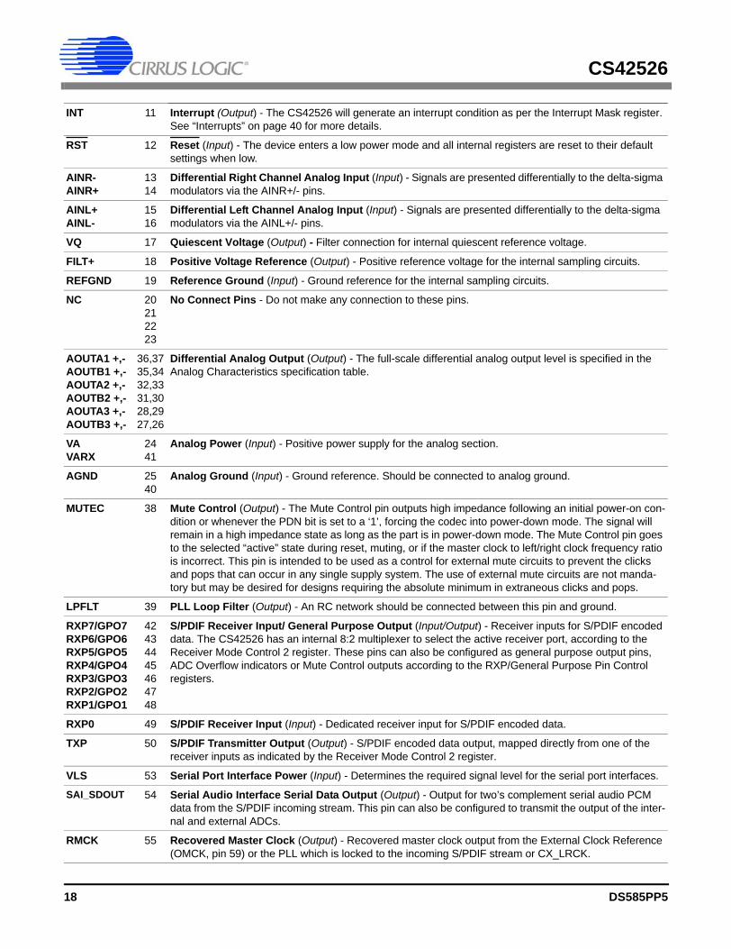
INT 11 Interrupt (Output) - The CS42526 will generate an interrupt condition as per the Interrupt Mask register. See “Interrupts” on page 40 for more details.
RST 12 Reset (Input) - The device enters a low power mode and all internal registers are reset to their default settings when low.
AINR-AINR+
1314
Differential Right Channel Analog Input (Input) - Signals are presented differentially to the delta-sigma modulators via the AINR+/- pins.
AINL+AINL-
1516
Differential Left Channel Analog Input (Input) - Signals are presented differentially to the delta-sigma modulators via the AINL+/- pins.
VQ 17 Quiescent Voltage (Output) - Filter connection for internal quiescent reference voltage.
FILT+ 18 Positive Voltage Reference (Output) - Positive reference voltage for the internal sampling circuits.
REFGND 19 Reference Ground (Input) - Ground reference for the internal sampling circuits.
NC 20212223
No Connect Pins - Do not make any connection to these pins.
AOUTA1 +,-AOUTB1 +,-AOUTA2 +,-AOUTB2 +,-AOUTA3 +,-AOUTB3 +,-
36,3735,3432,3331,3028,2927,26
Differential Analog Output (Output) - The full-scale differential analog output level is specified in the Analog Characteristics specification table.
VA VARX
2441
Analog Power (Input) - Positive power supply for the analog section.
AGND 2540
Analog Ground (Input) - Ground reference. Should be connected to analog ground.
MUTEC 38 Mute Control (Output) - The Mute Control pin outputs high impedance following an initial power-on con-dition or whenever the PDN bit is set to a ‘1’, forcing the codec into power-down mode. The signal will remain in a high impedance state as long as the part is in power-down mode. The Mute Control pin goes to the selected “active” state during reset, muting, or if the master clock to left/right clock frequency ratio is incorrect. This pin is intended to be used as a control for external mute circuits to prevent the clicks and pops that can occur in any single supply system. The use of external mute circuits are not manda-tory but may be desired for designs requiring the absolute minimum in extraneous clicks and pops.
LPFLT 39 PLL Loop Filter (Output) - An RC network should be connected between this pin and ground.
RXP7/GPO7RXP6/GPO6RXP5/GPO5RXP4/GPO4RXP3/GPO3RXP2/GPO2RXP1/GPO1
42434445464748
S/PDIF Receiver Input/ General Purpose Output (Input/Output) - Receiver inputs for S/PDIF encoded data. The CS42526 has an internal 8:2 multiplexer to select the active receiver port, according to the Receiver Mode Control 2 register. These pins can also be configured as general purpose output pins, ADC Overflow indicators or Mute Control outputs according to the RXP/General Purpose Pin Control registers.
RXP0 49 S/PDIF Receiver Input (Input) - Dedicated receiver input for S/PDIF encoded data.
TXP 50 S/PDIF Transmitter Output (Output) - S/PDIF encoded data output, mapped directly from one of the receiver inputs as indicated by the Receiver Mode Control 2 register.
VLS 53 Serial Port Interface Power (Input) - Determines the required signal level for the serial port interfaces.
SAI_SDOUT 54 Serial Audio Interface Serial Data Output (Output) - Output for two’s complement serial audio PCM data from the S/PDIF incoming stream. This pin can also be configured to transmit the output of the inter-nal and external ADCs.
RMCK 55 Recovered Master Clock (Output) - Recovered master clock output from the External Clock Reference (OMCK, pin 59) or the PLL which is locked to the incoming S/PDIF stream or CX_LRCK.
18 DS585PP5
CS42526
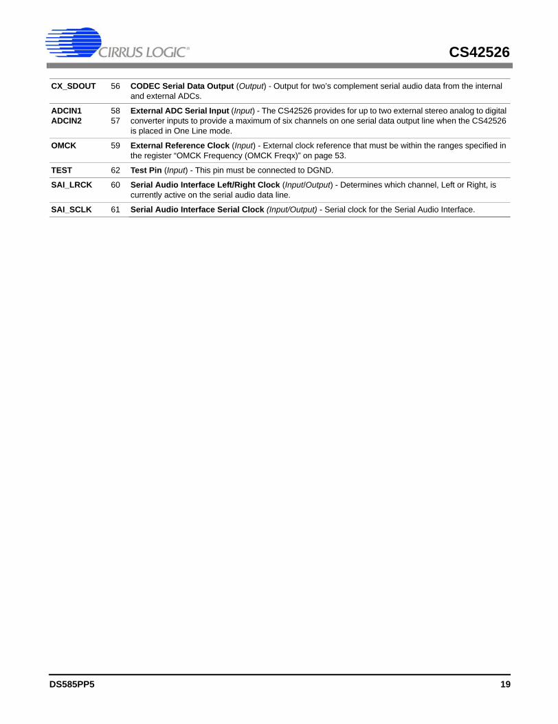
CX_SDOUT 56 CODEC Serial Data Output (Output) - Output for two’s complement serial audio data from the internal and external ADCs.
ADCIN1ADCIN2
5857
External ADC Serial Input (Input) - The CS42526 provides for up to two external stereo analog to digital converter inputs to provide a maximum of six channels on one serial data output line when the CS42526 is placed in One Line mode.
OMCK 59 External Reference Clock (Input) - External clock reference that must be within the ranges specified in the register “OMCK Frequency (OMCK Freqx)” on page 53.
TEST 62 Test Pin (Input) - This pin must be connected to DGND.
SAI_LRCK 60 Serial Audio Interface Left/Right Clock (Input/Output) - Determines which channel, Left or Right, is currently active on the serial audio data line.
SAI_SCLK 61 Serial Audio Interface Serial Clock (Input/Output) - Serial clock for the Serial Audio Interface.
DS585PP5 19
CS42526
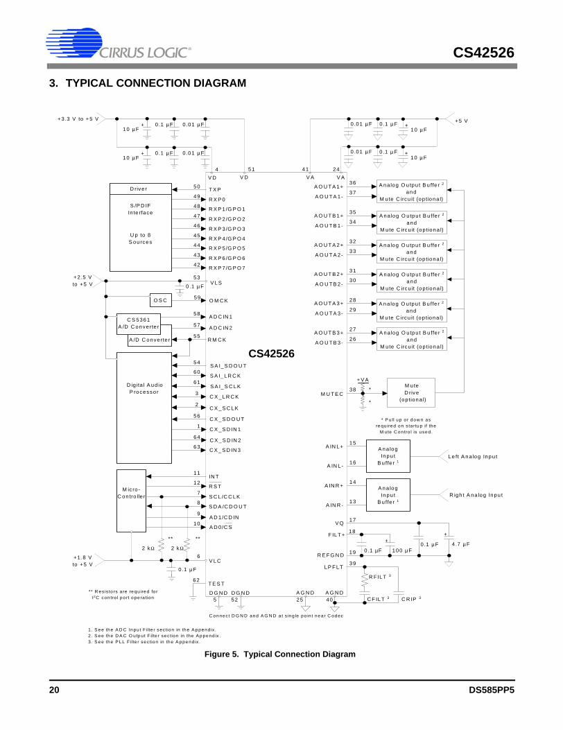
3. TYPICAL CONNECTION DIAGRAM
V D
A O U T A 1+
24
0 .1 µ F +10 µ F
10 0 µ F0 .1 µ F
++
17
18V Q
F ILT +
36
37
0 .1 µF4 .7 µ F
V A
+10 µ F
51
A O U T A 1-
A O U T B 1+35
34A O U T B 1-
A O U T A 2+32
33A O U T A 2-
A O U T B 2+31
30A O U T B 2-
A O U T A 3+ 28
29A O U T A 3-
A O U T B 3+27
26A O U T B 3-
M U T E C38
25D G N D D G N D
5
R E F G N D 19
414V AV D
0.1 µ F
A G N DA G N D52 40
LP F LT39
A IN L+
A IN L-
A IN R +
A IN R -
15
16
14
13
C o nnec t D G N D an d A G N D a t s ing le po in t ne a r C od ec
0 .01 µ F
0 .1 µ F +10 µ F
+ 5 V0 .01 µ F
0 .01 µ F
+ 3 .3 V to + 5 V+
10 µ F0 .1 µ F 0 .01 µ F
V LS0 .1 µ F
+2 .5 Vto +5 V
53
V LC0 .1 µ F
+1 .8 Vto +5 V
6
3
60
59
1
64
61
2
63
8
7S C L /C C LK
S D A /C D O U T
A D 1/C D IN
R S T12
9
O M C K
C X _S D IN 1
S A I_LR C K
S A I_S C LK
C X _S D IN 3
C X _S D IN 2
C X _LR C K
C X _S C LK
A D 0/C S10
IN T11
D ig ita l A ud ioP rocesso r
M ic ro -C on tro lle r
55R M C K
58 A D C IN 157 A D C IN 2
C S 53 61A /D C onve rte r
C S 5361A /D C onve rte r
56 C X _S D O U T
54S A I_S D O U T
48
46
49
44
45
47
R X P 0
R X P 1 /G P O 1S /P D IF
In te rface
50 T X PD rive r
U p to 8S ou rces
43
R X P 2 /G P O 2
R X P 3 /G P O 3
R X P 4 /G P O 4
R X P 5 /G P O 5
R X P 6 /G P O 6
R X P 7 /G P O 742
O S C
A na log O u tpu t B u ffe r 2
an dM ute C ircu it (op tio na l)
M u teD rive
(op tiona l)
2700 pF *
2700 pF *
Le ft A na log Inpu t
R igh t A na log Inpu tA na log
In pu tB u ffe r 1
A na logIn pu t
B u ffe r 1
+ V A
*
* P u ll up o r do w n asre qu ire d on s ta rtu p if the
M ute C on tro l is use d .
*
A na log O u tpu t B u ffe r 2
andM ute C ircu it (op tiona l)
A na log O u tpu t B u ffe r 2
andM ute C ircu it (op tiona l)
A na log O u tpu t B u ffe r 2
andM ute C ircu it (op tiona l)
A n a log O u tpu t B u ffe r 2
andM ute C ircu it (op tiona l)
A na log O u tpu t B u ffe r 2
andM ute C ircu it (op tiona l)
2 k Ω 2 k Ω
** **
C F ILT 3
R F ILT 3
C R IP 3
** R es is to rs a re requ ired fo rI2C con tro l po rt o pe ra tion
1 . S e e the A D C Inpu t F ilte r sec tion in the A pp end ix .2 . S e e the D A C O u tp u t F ilte r sec tion in the A p pend ix .3 . S e e the P LL F ilte r sec tion in the A ppe nd ix .
62T E S T
Figure 5. Typical Connection Diagram
CS42526
20 DS585PP5
CS42526
4. APPLICATIONS4.1 OverviewThe CS42526 is a highly integrated mixed signal 24-bit audio codec comprised of 2 analog-to-digital con-verters (ADC), implemented using multi-bit delta-sigma techniques, 6 digital-to-analog converters (DAC)and a 192 kHz digital audio S/PDIF receiver. Other functions integrated within the codec include indepen-dent digital volume controls for each DAC, digital de-emphasis filters for DAC and S/PDIF, digital gaincontrol for ADC channels, ADC high-pass filters, an on-chip voltage reference, and an 8:2 mux for S/PDIFsources. All serial data is transmitted through two configurable serial audio interfaces with standard serialinterface support as well as enhanced one line modes of operation allowing up to 6 channels of serial au-dio data on one data line. All functions are configured through a serial control port operable in SPI modeor in I2C mode. Figure 5 show the recommended connections for the CS42526.The CS42526 operates in one of three oversampling modes based on the input sample rate. Mode selec-tion is determined by the FM bits in register “Functional Mode (address 03h)” on page 48. Single-Speedmode (SSM) supports input sample rates up to 50 kHz and uses a 128x oversampling ratio. Double-Speed mode (DSM) supports input sample rates up to 100 kHz and uses an oversampling ratio of 64x.Quad-Speed mode (QSM) supports input sample rates up to 192 kHz and uses an oversampling ratio of32x.Using the receiver clock recovery PLL, a low jitter clock is recovered from the incoming S/PDIF datastream. The recovered clock or an externally supplied clock attached to the OMCK pin can be used asthe System Clock.
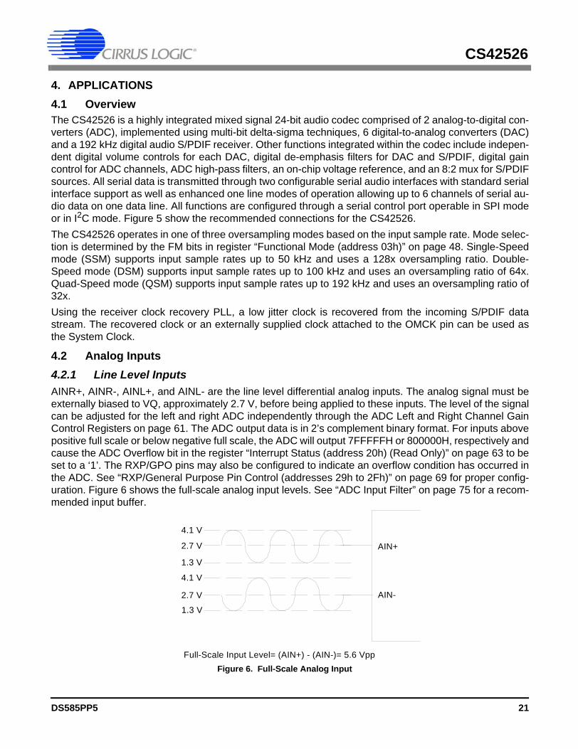
4.2 Analog Inputs4.2.1 Line Level InputsAINR+, AINR-, AINL+, and AINL- are the line level differential analog inputs. The analog signal must beexternally biased to VQ, approximately 2.7 V, before being applied to these inputs. The level of the signalcan be adjusted for the left and right ADC independently through the ADC Left and Right Channel GainControl Registers on page 61. The ADC output data is in 2’s complement binary format. For inputs abovepositive full scale or below negative full scale, the ADC will output 7FFFFFH or 800000H, respectively andcause the ADC Overflow bit in the register “Interrupt Status (address 20h) (Read Only)” on page 63 to beset to a ‘1’. The RXP/GPO pins may also be configured to indicate an overflow condition has occurred inthe ADC. See “RXP/General Purpose Pin Control (addresses 29h to 2Fh)” on page 69 for proper config-uration. Figure 6 shows the full-scale analog input levels. See “ADC Input Filter” on page 75 for a recom-mended input buffer.
AIN+
AIN-
Full-Scale Input Level= (AIN+) - (AIN-)= 5.6 Vpp
4.1 V
2.7 V
1.3 V
4.1 V
2.7 V
1.3 V
Figure 6. Full-Scale Analog Input
DS585PP5 21
CS42526
4.2.2 High Pass Filter and DC Offset CalibrationThe high pass filter continuously subtracts a measure of the DC offset from the output of the decimationfilter. The high pass filter can be independently enabled and disabled. If the HPF_Freeze bit is set duringnormal operation, the current value of the DC offset for the corresponding channel is frozen and this DCoffset will continue to be subtracted from the conversion result. This feature makes it possible to performa system DC offset calibration by:1) Running the CS42526 with the high pass filter enabled until the filter settles. See the Digital Filter
Characteristics for filter settling time. 2) Disabling the high pass filter and freezing the stored DC offset.The high pass filters are controlled using the HPF_FREEZE bit in the register “Misc Control (address 05h)”on page 51.
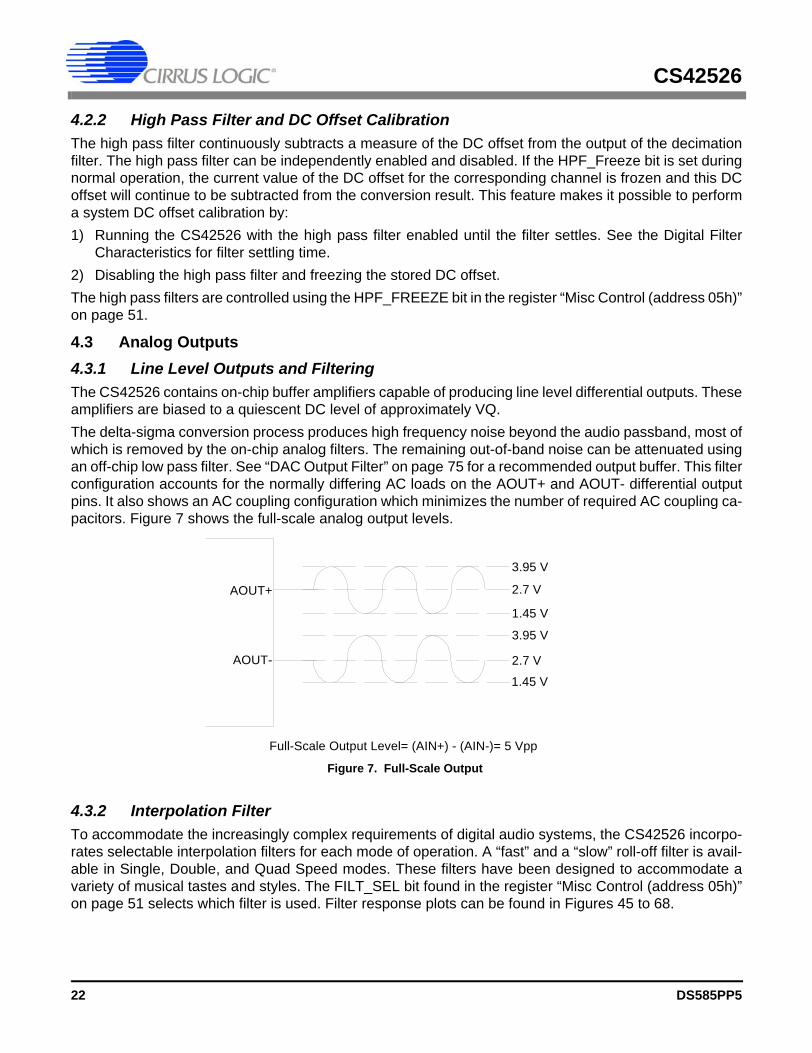
4.3 Analog Outputs4.3.1 Line Level Outputs and FilteringThe CS42526 contains on-chip buffer amplifiers capable of producing line level differential outputs. Theseamplifiers are biased to a quiescent DC level of approximately VQ. The delta-sigma conversion process produces high frequency noise beyond the audio passband, most ofwhich is removed by the on-chip analog filters. The remaining out-of-band noise can be attenuated usingan off-chip low pass filter. See “DAC Output Filter” on page 75 for a recommended output buffer. This filterconfiguration accounts for the normally differing AC loads on the AOUT+ and AOUT- differential outputpins. It also shows an AC coupling configuration which minimizes the number of required AC coupling ca-pacitors. Figure 7 shows the full-scale analog output levels.
4.3.2 Interpolation FilterTo accommodate the increasingly complex requirements of digital audio systems, the CS42526 incorpo-rates selectable interpolation filters for each mode of operation. A “fast” and a “slow” roll-off filter is avail-able in Single, Double, and Quad Speed modes. These filters have been designed to accommodate avariety of musical tastes and styles. The FILT_SEL bit found in the register “Misc Control (address 05h)”on page 51 selects which filter is used. Filter response plots can be found in Figures 45 to 68.
AOUT+
AOUT-
Full-Scale Output Level= (AIN+) - (AIN-)= 5 Vpp
3.95 V
2.7 V
1.45 V
3.95 V
2.7 V
1.45 V
Figure 7. Full-Scale Output
22 DS585PP5
CS42526
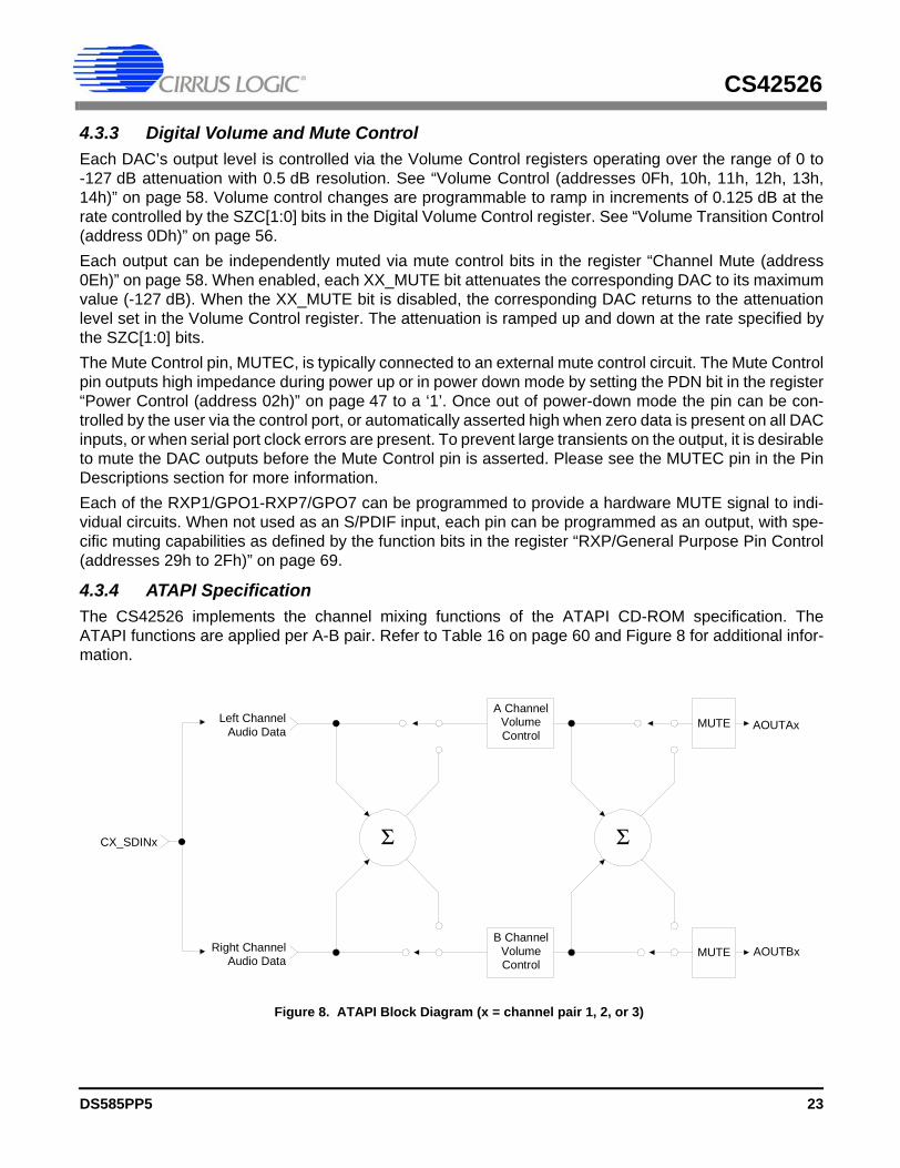
4.3.3 Digital Volume and Mute ControlEach DAC’s output level is controlled via the Volume Control registers operating over the range of 0 to-127 dB attenuation with 0.5 dB resolution. See “Volume Control (addresses 0Fh, 10h, 11h, 12h, 13h,14h)” on page 58. Volume control changes are programmable to ramp in increments of 0.125 dB at therate controlled by the SZC[1:0] bits in the Digital Volume Control register. See “Volume Transition Control(address 0Dh)” on page 56.Each output can be independently muted via mute control bits in the register “Channel Mute (address0Eh)” on page 58. When enabled, each XX_MUTE bit attenuates the corresponding DAC to its maximumvalue (-127 dB). When the XX_MUTE bit is disabled, the corresponding DAC returns to the attenuationlevel set in the Volume Control register. The attenuation is ramped up and down at the rate specified bythe SZC[1:0] bits.The Mute Control pin, MUTEC, is typically connected to an external mute control circuit. The Mute Controlpin outputs high impedance during power up or in power down mode by setting the PDN bit in the register“Power Control (address 02h)” on page 47 to a ‘1’. Once out of power-down mode the pin can be con-trolled by the user via the control port, or automatically asserted high when zero data is present on all DACinputs, or when serial port clock errors are present. To prevent large transients on the output, it is desirableto mute the DAC outputs before the Mute Control pin is asserted. Please see the MUTEC pin in the PinDescriptions section for more information.Each of the RXP1/GPO1-RXP7/GPO7 can be programmed to provide a hardware MUTE signal to indi-vidual circuits. When not used as an S/PDIF input, each pin can be programmed as an output, with spe-cific muting capabilities as defined by the function bits in the register “RXP/General Purpose Pin Control(addresses 29h to 2Fh)” on page 69.
4.3.4 ATAPI SpecificationThe CS42526 implements the channel mixing functions of the ATAPI CD-ROM specification. TheATAPI functions are applied per A-B pair. Refer to Table 16 on page 60 and Figure 8 for additional infor-mation.
Σ Σ
A ChannelVolumeControl
AOUTAx
AOUTBx
Left ChannelAudio Data
Right ChannelAudio Data
B ChannelVolumeControl
MUTE
MUTE
CX_SDINx
Figure 8. ATAPI Block Diagram (x = channel pair 1, 2, or 3)
DS585PP5 23
CS42526
4.4 S/PDIF ReceiverThe CS42526 includes an S/PDIF digital audio receiver. The S/PDIF receiver accepts and decodes digitalaudio data according to the IEC60958 (S/PDIF), and EIAJ CP-1201 interface standards. The receiver con-sists of an 8:2 multiplexer input stage driven through pins RXP0 and RXP1/GPO1 - RXP7/GPO7, a PLLbased clock recovery circuit, and a decoder which separates the audio data from the channel status anduser data. A comprehensive buffering scheme provides read access to the channel status and user data.External components are used to terminate and isolate the incoming data cables from the CS42526.These components and required circuitry are detailed in the CDB42528.
4.4.1 8:2 S/PDIF Input MultiplexerThe CS42526 contains an 8:2 S/PDIF Input Multiplexer to accommodate up to eight channels of input dig-ital audio data. Digital audio data is single-ended and input through the RXP0 andRXP1/GPO1-RXP7/GPO7 pins. Any one of these inputs can be multiplexed to the input of the S/PDIFreceiver and to the S/PDIF output pin TXP. When any portion of the multiplexer is implemented, unused RXP0 and RXPx/GPOx pins should be tiedto a 0.01uF capacitor to ground. The receiver multiplexer select line control is accessed through bitsRMUX2:0 in the Receiver Mode Control 2 register on page 62. The TXP multiplexer select line control isaccessed through bits TMUX2:0 in the same register. The multiplexer defaults to RXP0 for both functions.
4.4.2 Error Reporting and Hold FunctionWhile decoding the incoming S/PDIF data stream, the CS42526 can identify several kinds of error, indi-cated in the register “Receiver Errors (address 26h) (Read Only)” on page 67. See “Error Reporting andHold Function” on page 76 for more information.
4.4.3 Channel Status Data HandlingThe first 2 bytes of the Channel Status block (C data) are decoded into the Receiver Channel Status reg-ister (See “Receiver Channel Status (address 25h) (Read Only)” on page 66). See “Channel Status DataHandling” on page 76 for more information.
4.4.4 User Data HandlingThe incoming User (U) data is buffered in a user accessible buffer. If the U data bits have been encodedas Q-channel subcode, the data is decoded and presented in 10 consecutive register locations, address30h to 39h. The user can configure the Interrupt Mask Register to cause interrupts to indicate the decod-ing of a new Q-channel block, which may be read through the control port. See “User (U) Data E BufferAccess” on page 78 for more information.
4.4.5 Non-Audio Auto-DetectionAn S/PDIF data stream may be used to convey non-audio data, thus it is important to know whether theincoming data stream is digital PCM audio samples or not. This information is typically conveyed in chan-nel status bit 1 (AUDIO), which is extracted automatically by the CS42526. Certain non-audio sources,however, such as AC-3® or MPEG encoders, may not adhere to this convention, and the bit may not beproperly set. See “Non-Audio Auto-Detection” on page 78 for more information including details for inter-face format detection.
24 DS585PP5
CS42526
4.5 Clock GenerationThe clock generation for the CS42526 is shown in the figure below. The internal MCLK is derived from theoutput of the PLL or a master clock source attached to OMCK. The mux selection is controlled by theSW_CTRLx bits and can be configured to manual switch mode only, or automatically switch on loss ofPLL lock to the other source input.
4.5.1 PLL and Jitter AttenuationAn on-chip Phase Locked Loop (PLL) is used to recover the clock from the incoming S/PDIF data stream.There are some applications where low jitter in the recovered clock, presented on the RMCK pin, is im-portant. For this reason, the PLL has been designed to have good jitter attenuation characteristics asshown in Figure 28 on page 80. The PLL can be configured to lock onto the incoming SAI_LRCK signal from the Serial Audio InterfacePort and generate the required internal master clock frequency. By setting the PLL_LRCK bit to a ‘1’ inthe register “Clock Control (address 06h)” on page 52, the PLL will lock to the incoming SAI_LRCK andgenerate an output master clock (RMCK) of 256Fs. Table 2 shows the output of the PLL with typical inputFs values for SAI_LRCK. See “Appendix C: PLL Filter” on page 79 for more information concerning PLL operation, required filtercomponents, optimal layout guidelines and jitter attenuation characteristics.
SAI_LRCK(slave mode)
RecoveredS/PDIF Clock
0
1
PLL (256Fs)8.192 -
49.152 MHz
00
01
PLL_LRCK bit SW_CTRLx bits(manual or auto
switch)OMCK
Auto DetectInput Clock 1,1.5, 2, 4
singlespeed
256
doublespeed
128
quadspeed
64
singlespeed
4
doublespeed
2
quadspeed
1
000110
000110
000110
000110
not OLM
OLM #1
CODEC_FMx bits
SAI_FMx bits
DAC_OLxor ADC_OLx bits
ADC_OLx andADC_SP SELx bits
SAI_SCLK
CX_SCLK
CX_LRCK
SAI_LRCK
RMCK
OLM #2
not OLM
OLM #1
OLM #2
128FS
256FS
128FS
256FS
InternalMCLK
00011011
RMCK_DIVx bits
2
4
X2
Figure 9. CS42526 Clock Generation
DS585PP5 25
CS42526
4.5.2 OMCK System Clock ModeA special clock switching mode is available that allows the clock that is input through the OMCK pin to beused as the internal master clock. This feature is controlled by the SW_CTRLx bits in register “Clock Con-trol (address 06h)” on page 52. An advanced auto switching mode is also implemented to maintain masterclock functionality. The clock auto switching mode allows the clock input through OMCK to be used as aclock in the system without any disruption when the PLL loses lock; for example, when the input is re-moved from the receiver. This clock switching is done glitch free. A clock adhering to the specificationsdetailed in the Switching Characteristics table on page 12 must be applied to the OMCK pin at all timesthat the FRC_PLL_LK bit is set to ‘0’ (See “Force PLL Lock (FRC_PLL_LK)” on page 53).
4.5.3 Master ModeIn master mode, the serial interface timings are derived from an external clock attached to OMCK or theoutput of the PLL with an input reference to either the S/PDIF Receiver recovered clock or the SAI_LRCKinput from the Serial Audio Interface Port. Master clock selection and operation is configured with theSW_CTRL1:0 bits in the Clock Control Register (See “Clock Control (address 06h)” on page 52).The supported PLL output frequencies are shown in Table 2 below.
4.5.4 Slave ModeIn Slave mode, CX_LRCK, CX_SCLK and/or SAI_LRCK, SAI_SCLK operate as inputs. The Left/Rightclock signal must be equal to the sample rate, Fs, and must be synchronously derived from the suppliedmaster clock, OMCK or the output of the PLL. The serial bit clock, CX_SCLK and/or SAI_SCLK, must besynchronously derived from the master clock and be equal to 128x, 64x, 48x or 32x Fs depending on theinterface format selected and desired speed mode. One Line Mode #1 is supported in Slave Mode. OneLine Mode #2 is not supported. Refer to Table 3 for required clock ratios. The sample rate to OMCK ratiosand OMCK frequency requirements for Slave mode operation are shown in Table 1.
Single Speed Double Speed Quad Speed One Line Mode #1OMCK/LRCK Ratio 256x, 384x, 512x 128x, 192x, 256x 64x, 96x, 128x 256x
Table 3. Slave Mode Clock Ratios
Sample Rate(kHz)
OMCK (MHz)Single Speed(4 to 50 kHz)
Double Speed(50 to 100 kHz)
Quad Speed(100 to 192 kHz)
256x 384x 512x 128x 192x 256x 64x 96x 128x48 12.2880 18.4320 24.5760 - - - - - -96 - - - 12.2880 18.4320 24.5760 - - -
192 - - - - - - 12.2880 18.4320 24.5760Table 1. Common OMCK Clock Frequencies
Sample Rate(kHz)
PLL Output (MHz)Single Speed(4 to 50 kHz)
Double Speed(50 to 100 kHz)
Quad Speed(100 to 192 kHz)
256x 256x 256x32 8.1920 - -
44.1 11.2896 - -48 12.2880 - -64 - 16.3840 -
88.2 - 22.5792 -96 - 24.5760 -
176.4 - - 45.1584192 - - 49.1520
Table 2. Common PLL Output Clock Frequencies
26 DS585PP5
CS42526
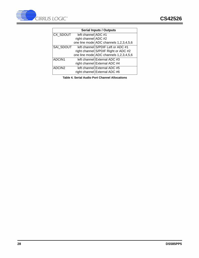
4.6 Digital Interfaces4.6.1 Serial Audio Interface SignalsThe CS42526 interfaces to an external Digital Audio Processor via two independent serial ports, theCODEC serial port, CODEC_SP and the Serial Audio Interface serial port, SAI_SP. The digital output ofthe internal ADCs can be configured to use either the CX_SDOUT pin or the SAI_SDOUT pin and thecorresponding serial port clocking signals. These configuration bits and the selection of Single, Double orQuad-Speed mode for CODEC_SP and SAI_SP are found in register “Functional Mode (address 03h)”on page 48. The serial interface clocks, SAI_SCLK for SAI_SP and CX_SCLK for CODEC_SP, are used for transmit-ting and receiving audio data. Either SAI_SCLK or CX_SCLK can be generated by the CS42526 (mastermode) or it can be input from an external source (slave mode). Master or Slave mode selection is madeusing bits CODEC_SP M/S and SAI_SP M/S in register “Misc Control (address 05h)” on page 51. The Left/Right clock (SAI_LRCK or CX_LRCK) is used to indicate left and right data frames and the startof a new sample period. It may be an output of the CS42526 (master mode), or it may be generated byan external source (slave mode). As described in later sections, particular modes of operation do allowthe sample rate, Fs, of the SAI_SP and the CODEC_SP to be different, but must be multiples of eachother.The serial data interface format selection (left/right justified, I2S or one line mode) for the Serial Audio In-terface serial port data out pin, SAI_SDOUT, the CODEC serial port data out pin, CX_SDOUT, and theCODEC input pins, CX_SDIN1:3, is configured using the appropriate bits in the register “Interface For-mats (address 04h)” on page 49. The serial audio data is presented in 2's complement binary form withthe MSB first in all formats.CX_SDIN1, CX_SDIN2, and CX_SDIN3 are the serial data input pins supplying the associated internalDAC. CX_SDOUT, the ADC data output pin, carries data from the two internal 24-bit ADCs and, whenconfigured for one-line mode, up to four additional ADC channels attached externally to the signalsADCIN1 and ADCIN2 (typically two CS5361 stereo ADCs). When operated in One Line Mode, 6 channelsof DAC data are input on CX_SDIN1 and 6 channels of ADC data are output on CX_SDOUT. Table 4outlines the serial port channel allocations.
SCLK/LRCK Ratio 32x, 48x, 64x, 128x 32x, 48x, 64x 32x, 48x, 64x 128x
Serial Inputs / OutputsCX_SDIN1 left channel right channel
one line mode
DAC #1DAC #2DAC channels 1,2,3,4,5,6
CX_SDIN2 left channel right channel one line mode
DAC #3DAC #4not used
CX_SDIN3 left channel right channel one line mode
DAC #5DAC #6not used
Table 4. Serial Audio Port Channel Allocations
Single Speed Double Speed Quad Speed One Line Mode #1
Table 3. Slave Mode Clock Ratios
DS585PP5 27
CS42526
CX_SDOUT left channel right channel
one line mode
ADC #1ADC #2ADC channels 1,2,3,4,5,6
SAI_SDOUT left channel right channel
one line mode
S/PDIF Left or ADC #1S/PDIF Right or ADC #2ADC channels 1,2,3,4,5,6
ADCIN1 left channel right channel
External ADC #3External ADC #4
ADCIN2 left channel right channel
External ADC #5External ADC #6
Serial Inputs / Outputs
Table 4. Serial Audio Port Channel Allocations
28 DS585PP5
CS42526
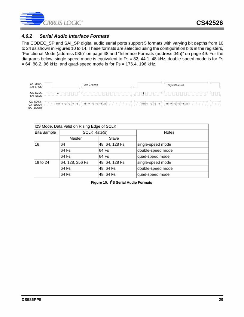
4.6.2 Serial Audio Interface FormatsThe CODEC_SP and SAI_SP digital audio serial ports support 5 formats with varying bit depths from 16to 24 as shown in Figures 10 to 14. These formats are selected using the configuration bits in the registers,“Functional Mode (address 03h)” on page 48 and “Interface Formats (address 04h)” on page 49. For thediagrams below, single-speed mode is equivalent to Fs = 32, 44.1, 48 kHz; double-speed mode is for Fs= 64, 88.2, 96 kHz; and quad-speed mode is for Fs = 176.4, 196 kHz.
Left Channel Right Channel
CX_SDINxCX_SDOUTSAI_SDOUT
+3 +2 +1+5 +4-1 -2 -3 -4 -5 +3 +2 +1+5 +4-1 -2 -3 -4MSB MSBLSB LSB
CX_LRCKSAI_LRCK
CX_SCLKSAI_SCLK
Figure 10. I2S Serial Audio Formats
I2S Mode, Data Valid on Rising Edge of SCLKBits/Sample SCLK Rate(s) Notes
Master Slave16 64 48, 64, 128 Fs single-speed mode
64 Fs 64 Fs double-speed mode64 Fs 64 Fs quad-speed mode
18 to 24 64, 128, 256 Fs 48, 64, 128 Fs single-speed mode64 Fs 48, 64 Fs double-speed mode64 Fs 48, 64 Fs quad-speed mode
DS585PP5 29
CS42526
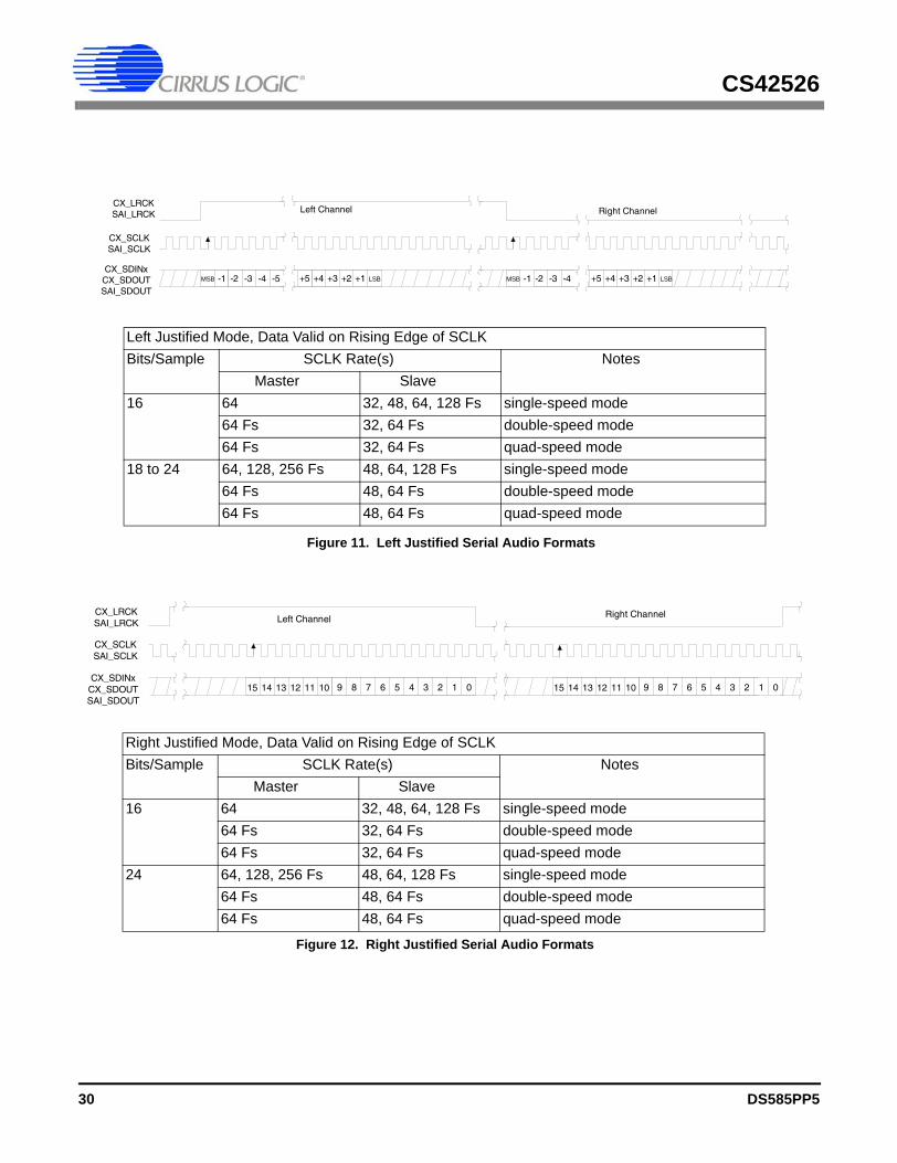
CX_LRCKSAI_LRCK
CX_SCLKSAI_SCLK
Left Channel Right Channel
CX_SDINxCX_SDOUTSAI_SDOUT
+3 +2 +1+5 +4-1 -2 -3 -4 -5 +3 +2 +1+5 +4-1 -2 -3 -4MSB LSB MSB LSB
Figure 11. Left Justified Serial Audio Formats
Left Justified Mode, Data Valid on Rising Edge of SCLKBits/Sample SCLK Rate(s) Notes
Master Slave16 64 32, 48, 64, 128 Fs single-speed mode
64 Fs 32, 64 Fs double-speed mode64 Fs 32, 64 Fs quad-speed mode
18 to 24 64, 128, 256 Fs 48, 64, 128 Fs single-speed mode64 Fs 48, 64 Fs double-speed mode64 Fs 48, 64 Fs quad-speed mode
Left Channel Right Channel
6 5 4 3 2 1 09 8 715 14 13 12 11 10 6 5 4 3 2 1 09 8 715 14 13 12 11 10CX_SDINx
CX_SDOUTSAI_SDOUT
CX_LRCKSAI_LRCK
CX_SCLKSAI_SCLK
Figure 12. Right Justified Serial Audio Formats
Right Justified Mode, Data Valid on Rising Edge of SCLKBits/Sample SCLK Rate(s) Notes
Master Slave16 64 32, 48, 64, 128 Fs single-speed mode
64 Fs 32, 64 Fs double-speed mode64 Fs 32, 64 Fs quad-speed mode
24 64, 128, 256 Fs 48, 64, 128 Fs single-speed mode64 Fs 48, 64 Fs double-speed mode64 Fs 48, 64 Fs quad-speed mode
30 DS585PP5
CS42526
CX_LRCKSAI_LRCK
CX_SCLKSAI_SCLK
LSBMSB
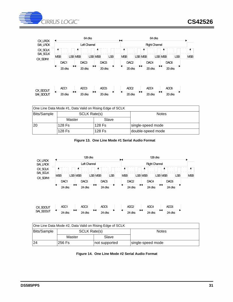
20clks
64clks 64clks
LSBMSB LSBMSB LSBMSB LSBMSB LSBMSB MSB
DAC1 DAC3 DAC5 DAC2 DAC4 DAC6
20clks 20clks 20clks 20clks 20clks
Left Channel Right Channel
20clks
ADC1 ADC3 ADC5 ADC2 ADC4 ADC6
20clks 20clks 20clks 20clks 20clksCX_SDOUTSAI_SDOUT
CX_SDIN1
Figure 13. One Line Mode #1 Serial Audio Format
One Line Data Mode #1, Data Valid on Rising Edge of SCLKBits/Sample SCLK Rate(s) Notes
Master Slave20 128 Fs 128 Fs single-speed mode
128 Fs 128 Fs double-speed mode
CX_LRCKSAI_LRCK
CX_SCLKSAI_SCLK
LSBMSB
24clks
128 clks
LSBMSB LSBMSB LSBMSB LSBMSB LSBMSB MSB
DAC1 DAC3 DAC5 DAC2 DAC4 DAC6
24clks 24clks 24clks 24clks 24clks
Left Channel Right Channel
24clks
ADC1 ADC3 ADC5 ADC2 ADC4 ADC6
24clks 24clks 24clks 24clks 24clks
CX_SDOUTSAI_SDOUT
128 clks
CX_SDIN1
Figure 14. One Line Mode #2 Serial Audio Format
One Line Data Mode #2, Data Valid on Rising Edge of SCLKBits/Sample SCLK Rate(s) Notes
Master Slave24 256 Fs not supported single-speed mode
DS585PP5 31
CS42526
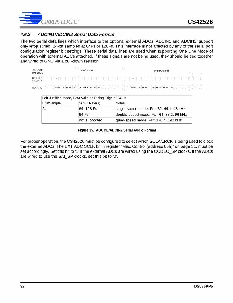
4.6.3 ADCIN1/ADCIN2 Serial Data FormatThe two serial data lines which interface to the optional external ADCs, ADCIN1 and ADCIN2, supportonly left-justified, 24-bit samples at 64Fs or 128Fs. This interface is not affected by any of the serial portconfiguration register bit settings. These serial data lines are used when supporting One Line Mode ofoperation with external ADCs attached. If these signals are not being used, they should be tied togetherand wired to GND via a pull-down resistor.
For proper operation, the CS42526 must be configured to select which SCLK/LRCK is being used to clockthe external ADCs. The EXT ADC SCLK bit in register “Misc Control (address 05h)” on page 51, must beset accordingly. Set this bit to ‘1’ if the external ADCs are wired using the CODEC_SP clocks. If the ADCsare wired to use the SAI_SP clocks, set this bit to ‘0’.
CX_LRCKSAI_LRCK
CX_SCLKSAI_SCLK
Left Channel Right Channel
ADCIN1/2 +3 +2 +1+5 +4-1 -2 -3 -4 -5 +3 +2 +1+5 +4-1 -2 -3 -4MSB LSB MSB LSB
Figure 15. ADCIN1/ADCIN2 Serial Audio Format
Left Justified Mode, Data Valid on Rising Edge of SCLKBits/Sample SCLK Rate(s) Notes24 64, 128 Fs single-speed mode, Fs= 32, 44.1, 48 kHz
64 Fs double-speed mode, Fs= 64, 88.2, 96 kHznot supported quad-speed mode, Fs= 176.4, 192 kHz
32 DS585PP5
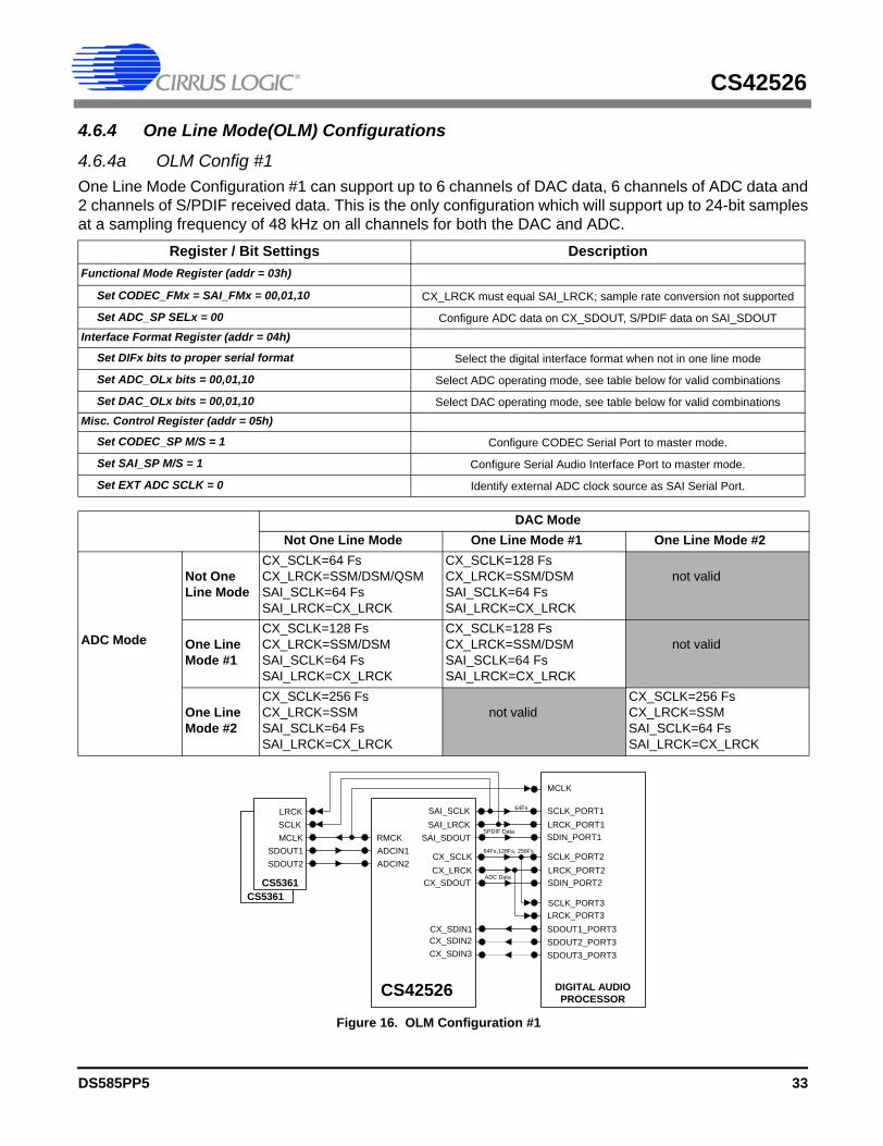
CS42526
4.6.4 One Line Mode(OLM) Configurations
4.6.4a OLM Config #1One Line Mode Configuration #1 can support up to 6 channels of DAC data, 6 channels of ADC data and2 channels of S/PDIF received data. This is the only configuration which will support up to 24-bit samplesat a sampling frequency of 48 kHz on all channels for both the DAC and ADC.
Register / Bit Settings DescriptionFunctional Mode Register (addr = 03h)
Set CODEC_FMx = SAI_FMx = 00,01,10 CX_LRCK must equal SAI_LRCK; sample rate conversion not supported
Set ADC_SP SELx = 00 Configure ADC data on CX_SDOUT, S/PDIF data on SAI_SDOUTInterface Format Register (addr = 04h)
Set DIFx bits to proper serial format Select the digital interface format when not in one line mode
Set ADC_OLx bits = 00,01,10 Select ADC operating mode, see table below for valid combinations
Set DAC_OLx bits = 00,01,10 Select DAC operating mode, see table below for valid combinationsMisc. Control Register (addr = 05h)
Set CODEC_SP M/S = 1 Configure CODEC Serial Port to master mode.
Set SAI_SP M/S = 1 Configure Serial Audio Interface Port to master mode.
Set EXT ADC SCLK = 0 Identify external ADC clock source as SAI Serial Port.
DAC Mode Not One Line Mode One Line Mode #1 One Line Mode #2
ADC Mode
Not One Line Mode
CX_SCLK=64 FsCX_LRCK=SSM/DSM/QSMSAI_SCLK=64 FsSAI_LRCK=CX_LRCK
CX_SCLK=128 FsCX_LRCK=SSM/DSMSAI_SCLK=64 FsSAI_LRCK=CX_LRCK
not valid
One Line Mode #1
CX_SCLK=128 FsCX_LRCK=SSM/DSMSAI_SCLK=64 FsSAI_LRCK=CX_LRCK
CX_SCLK=128 FsCX_LRCK=SSM/DSMSAI_SCLK=64 FsSAI_LRCK=CX_LRCK
not valid
One Line Mode #2
CX_SCLK=256 FsCX_LRCK=SSMSAI_SCLK=64 FsSAI_LRCK=CX_LRCK
not valid
CX_SCLK=256 FsCX_LRCK=SSMSAI_SCLK=64 FsSAI_LRCK=CX_LRCK
SCLK_PORT1LRCK_PORT1SDIN_PORT1
SCLK_PORT2LRCK_PORT2SDIN_PORT2
SCLK_PORT3LRCK_PORT3SDOUT1_PORT3SDOUT2_PORT3SDOUT3_PORT3
SAI_SCLKSAI_LRCK
SAI_SDOUT
CX_SCLKCX_LRCK
CX_SDOUT
CX_SDIN1CX_SDIN2CX_SDIN3
RMCKADCIN1ADCIN2
MCLKSDOUT1SDOUT2
LRCKSCLK
64Fs
SPDIF Data
ADC Data
64Fs,128Fs, 256Fs
DIGITAL AUDIOPROCESSOR
CS5361CS5361
MCLK
Figure 16. OLM Configuration #1
CS42526
DS585PP5 33
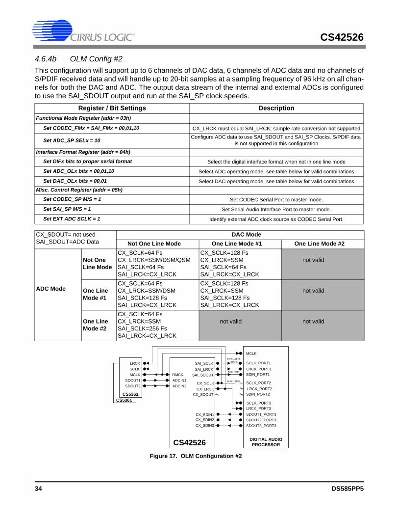
CS42526
4.6.4b OLM Config #2This configuration will support up to 6 channels of DAC data, 6 channels of ADC data and no channels ofS/PDIF received data and will handle up to 20-bit samples at a sampling frequency of 96 kHz on all chan-nels for both the DAC and ADC. The output data stream of the internal and external ADCs is configuredto use the SAI_SDOUT output and run at the SAI_SP clock speeds.
Register / Bit Settings DescriptionFunctional Mode Register (addr = 03h)
Set CODEC_FMx = SAI_FMx = 00,01,10 CX_LRCK must equal SAI_LRCK; sample rate conversion not supported
Set ADC_SP SELx = 10 Configure ADC data to use SAI_SDOUT and SAI_SP Clocks. S/PDIF data is not supported in this configuration
Interface Format Register (addr = 04h)
Set DIFx bits to proper serial format Select the digital interface format when not in one line mode
Set ADC_OLx bits = 00,01,10 Select ADC operating mode, see table below for valid combinations
Set DAC_OLx bits = 00,01 Select DAC operating mode, see table below for valid combinationsMisc. Control Register (addr = 05h)
Set CODEC_SP M/S = 1 Set CODEC Serial Port to master mode.
Set SAI_SP M/S = 1 Set Serial Audio Interface Port to master mode.
Set EXT ADC SCLK = 1 Identify external ADC clock source as CODEC Serial Port.
CX_SDOUT= not usedSAI_SDOUT=ADC Data
DAC Mode Not One Line Mode One Line Mode #1 One Line Mode #2
ADC Mode
Not One Line Mode
CX_SCLK=64 FsCX_LRCK=SSM/DSM/QSMSAI_SCLK=64 FsSAI_LRCK=CX_LRCK
CX_SCLK=128 FsCX_LRCK=SSMSAI_SCLK=64 FsSAI_LRCK=CX_LRCK
not valid
One Line Mode #1
CX_SCLK=64 FsCX_LRCK=SSM/DSMSAI_SCLK=128 FsSAI_LRCK=CX_LRCK
CX_SCLK=128 FsCX_LRCK=SSMSAI_SCLK=128 FsSAI_LRCK=CX_LRCK
not valid
One Line Mode #2
CX_SCLK=64 FsCX_LRCK=SSMSAI_SCLK=256 FsSAI_LRCK=CX_LRCK
not valid
not valid
SCLK_PORT1LRCK_PORT1SDIN_PORT1
SCLK_PORT2LRCK_PORT2
SDIN_PORT2
SCLK_PORT3LRCK_PORT3SDOUT1_PORT3SDOUT2_PORT3SDOUT3_PORT3
RMCKADCIN1ADCIN2
MCLKSDOUT1SDOUT2
LRCKSCLK
64Fs,128Fs
ADC Data
64Fs,128Fs,256Fs
DIGITAL AUDIOPROCESSOR
CS5361CS5361
SAI_SCLKSAI_LRCK
SAI_SDOUT
CX_SCLKCX_LRCK
CX_SDOUT
CX_SDIN1CX_SDIN2CX_SDIN3
MCLK
Figure 17. OLM Configuration #2
CS42526
34 DS585PP5
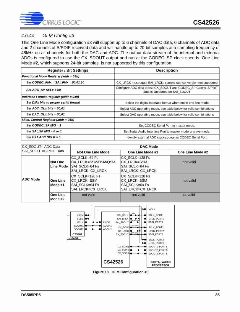
CS42526
4.6.4c OLM Config #3This One Line Mode configuration #3 will support up to 6 channels of DAC data, 6 channels of ADC dataand 2 channels of S/PDIF received data and will handle up to 20-bit samples at a sampling frequency of48kHz on all channels for both the DAC and ADC. The output data stream of the internal and externalADCs is configured to use the CX_SDOUT output and run at the CODEC_SP clock speeds. One LineMode #2, which supports 24-bit samples, is not supported by this configuration.
Register / Bit Settings DescriptionFunctional Mode Register (addr = 03h)
Set CODEC_FMx = SAI_FMx = 00,01,10 CX_LRCK must equal SAI_LRCK; sample rate conversion not supported
Set ADC_SP SELx = 00 Configure ADC data to use CX_SDOUT and CODEC_SP Clocks. S/PDIF data is supported on SAI_SDOUT
Interface Format Register (addr = 04h)
Set DIFx bits to proper serial format Select the digital interface format when not in one line mode
Set ADC_OLx bits = 00,01 Select ADC operating mode, see table below for valid combinations
Set DAC_OLx bits = 00,01 Select DAC operating mode, see table below for valid combinationsMisc. Control Register (addr = 05h)
Set CODEC_SP M/S = 1 Set CODEC Serial Port to master mode.
Set SAI_SP M/S = 0 or 1 Set Serial Audio Interface Port to master mode or slave mode.
Set EXT ADC SCLK = 1 Identify external ADC clock source as CODEC Serial Port.
CX_SDOUT= ADC DataSAI_SDOUT=S/PDIF Data
DAC Mode Not One Line Mode One Line Mode #1 One Line Mode #2
ADC Mode
Not One Line Mode
CX_SCLK=64 FsCX_LRCK=SSM/DSM/QSMSAI_SCLK=64 FsSAI_LRCK=CX_LRCK
CX_SCLK=128 FsCX_LRCK=SSMSAI_SCLK=64 FsSAI_LRCK=CX_LRCK
not valid
One Line Mode #1
CX_SCLK=128 FsCX_LRCK=SSMSAI_SCLK=64 FsSAI_LRCK=CX_LRCK
CX_SCLK=128 FsCX_LRCK=SSMSAI_SCLK=64 FsSAI_LRCK=CX_LRCK
not valid
One Line Mode #2
not valid not valid not valid
Figure 18. OLM Configuration #3
SCLK_PORT1LRCK_PORT1SDIN_PORT1
SCLK_PORT2LRCK_PORT2SDIN_PORT2
SCLK_PORT3LRCK_PORT3SDOUT1_PORT3SDOUT2_PORT3SDOUT3_PORT3
RMCKADCIN1ADCIN2
MCLKSDOUT1SDOUT2
LRCKSCLK
64Fs
SPDIF Data
ADC Data
64Fs,128Fs
DIGITAL AUDIOPROCESSOR
CS5361CS5361
SAI_SCLKSAI_LRCK
SAI_SDOUT
CX_SCLKCX_LRCK
CX_SDOUT
CX_SDIN1CX_SDIN2CX_SDIN3
MCLK
CS42526
DS585PP5 35
CS42526
4.6.4d OLM Config #4This configuration will support up to 6 channels of DAC data, 6 channels of ADC data and no channels ofS/PDIF received data. OLM Config #4 will handle up to 20-bit ADC samples at an Fs of 48 kHz and 24-bitDAC samples at an Fs of 48 kHz. Since the ADCs data stream is configured to use the SAI_SDOUT out-put and the internal and external ADCs are clocked from the SAI_SP, then the sample rate for the CODECSerial Port can be different from the sample rate of the Serial Audio Interface serial port.
Register / Bit Settings DescriptionFunctional Mode Register (addr = 03h)
Set CODEC_FMx = 00,01,10 CX_LRCK can run at SSM, DSM, or QSM independent of SAI_LRCK
Set SAI_FMx = 00,01,10 SAI_LRCK can run at SSM, DSM, or QSM independent of CX_LRCK
Set ADC_SP SELx = 10 Configure ADC data to use SAI_SDOUT and SAI_SP Clocks. S/PDIF data is not supported in this configuration
Interface Format Register (addr = 04h)
Set DIFx bits to proper serial format Select the digital interface format when not in one line mode
Set ADC_OLx bits = 00,01 Select ADC operating mode, see table below for valid combinations
Set DAC_OLx bits = 00,01,10 Select DAC operating mode, see table below for valid combinationsMisc. Control Register (addr = 05h)
Set CODEC_SP M/S = 1 Set DAC Serial Port to master mode.
Set SAI_SP M/S = 0 or 1 Set ADC Serial Port to master mode or slave mode.
Set EXT ADC SCLK = 0 Identify external ADC clock source as SAI Serial Port.
CX_SDOUT= not usedSAI_SDOUT=ADC Data
DAC Mode Not One Line Mode One Line Mode #1 One Line Mode #2
ADC Mode
Not One Line Mode
CX_SCLK=64 FsCX_LRCK=SSM/DSM/QSMSAI_SCLK=64 FsSAI_LRCK=SSM/DSM/QSM
CX_SCLK=128 FsCX_LRCK=SSM/DSMSAI_SCLK=64 FsSAI_LRCK=SSM/DSM/QSM
CX_SCLK=256 FsCX_LRCK=SSMSAI_SCLK=64 FsSAI_LRCK=SSM/DSM/QSM
One Line Mode #1
CX_SCLK=64 FsCX_LRCK=SSM/DSM/QSMSAI_SCLK=128 FsSAI_LRCK=SSM
CX_SCLK=128 FsCX_LRCK=SSM/DSMSAI_SCLK=128 FsSAI_LRCK=SSM
CX_SCLK=256 FsCX_LRCK=SSMSAI_SCLK=128 FsSAI_LRCK=SSM
One Line Mode #2
not valid not valid not valid
SCLK_PORT1LRCK_PORT1SDIN_PORT1
SCLK_PORT2LRCK_PORT2SDIN_PORT2
SCLK_PORT3LRCK_PORT3SDOUT1_PORT3SDOUT2_PORT3SDOUT3_PORT3
RMCKADCIN1ADCIN2
MCLKSDOUT1SDOUT2
LRCKSCLK
64Fs,128Fs,256Fs
ADC Data
64Fs,128Fs
DIGITAL AUDIOPROCESSOR
CS5361CS5361
SAI_SCLKSAI_LRCK
SAI_SDOUT
CX_SCLKCX_LRCK
CX_SDOUT
CX_SDIN1CX_SDIN2CX_SDIN3
MCLK
Figure 19. OLM Configuration #4
CS42526
36 DS585PP5
CS42526
4.6.4e OLM Config #5This One-Line Mode configuration can support up to 6 channels of DAC data, 2 channels of ADC dataand 2 channels of S/PDIF received data and will handle up to 24-bit samples at a sampling frequency of48 kHz on all channels for both the DAC and ADC. The output data stream of the internal ADCs can beconfigured to use the CX_SDOUT output and run at the CODEC_SP clock speeds or to use theSAI_SDOUT data output and run at the SAI_SP rate. The CODEC_SP and SAI_SP can operate at differ-ent Fs rates.
Register / Bit Settings DescriptionFunctional Mode Register (addr = 03h)
Set CODEC_FMx = 00,01,10 CX_LRCK can run at SSM, DSM, or QSM independent of SAI_LRCK
Set SAI_FMx = 00,01,10 SAI_LRCK can run at SSM, DSM, or QSM independent of CX_LRCK
Set ADC_SP SELx = 00,01,10 Configure ADC data to use CX_SDOUT and CODEC_SP clocks, or SAI_SDOUT and SAI_SP cocks.
Interface Format Register (addr = 04h)
Set DIFx bits to proper serial format Select the digital interface format when not in one line mode
Set ADC_OLx bits = 00 Set ADC operating mode to Not One Line Mode since only 2 channels of ADC are supported
Set DAC_OLx bits = 00,01 Select DAC operating mode, see table below for valid combinationsMisc. Control Register (addr = 05h)
Set CODEC_SP M/S = 0 or 1 Set CODEC Serial Port to master mode or slave mode.
Set SAI_SP M/S = 0 or 1 Set Serial Audio Interface Port to master mode or slave mode.
Set EXT ADC SCLK = 0 External ADCs are not used. Leave bit in default state.
CX_SDOUT= ADC DataSAI_SDOUT=ADC or S/PDIF Data
DAC Mode Not One Line Mode One Line Mode #1 One Line Mode #2
ADC Mode
Not One Line Mode
CX_SCLK=64 FsCX_LRCK=SSM/DSM/QSMSAI_SCLK=64 FsSAI_LRCK=SSM/DSM/QSM
CX_SCLK=128 FsCX_LRCK=SSM/DSMSAI_SCLK=64 FsSAI_LRCK=SSM/DSM/QSM
not valid
One Line Mode #1
not valid not valid not valid
One Line Mode #2
not valid not valid not valid
SCLK_PORT1LRCK_PORT1SDIN_PORT1
SCLK_PORT2LRCK_PORT2SDIN_PORT2
SCLK_PORT3LRCK_PORT3SDOUT1_PORT3SDOUT2_PORT3SDOUT3_PORT3
RMCKADCIN1ADCIN2
SPDIF or ADC Data
ADC Data
64Fs,128Fs, 256Fs
DIGITAL AUDIOPROCESSOR
SAI_SCLKSAI_LRCK
SAI_SDOUT
CX_SCLKCX_LRCK
CX_SDOUT
CX_SDIN1CX_SDIN2CX_SDIN3
64Fs,128Fs, 256Fs
MCLK
Figure 20. OLM Configuration #5
CS42526
DS585PP5 37
CS42526
4.7 Control Port Description and TimingThe control port is used to access the registers, allowing the CS42526 to be configured for the desiredoperational modes and formats. The operation of the control port may be completely asynchronous withrespect to the audio sample rates. However, to avoid potential interference problems, the control port pinsshould remain static if no operation is required.The control port has 2 modes: SPI and I2C, with the CS42526 acting as a slave device. SPI mode is se-lected if there is a high to low transition on the AD0/CS pin, after the RST pin has been brought high. I2Cmode is selected by connecting the AD0/CS pin through a resistor to VLC or DGND, thereby permanentlyselecting the desired AD0 bit address state.
4.7.1 SPI ModeIn SPI mode, CS is the CS42526 chip select signal, CCLK is the control port bit clock (input into theCS42526 from the microcontroller), CDIN is the input data line from the microcontroller, CDOUT is theoutput data line to the microcontroller. Data is clocked in on the rising edge of CCLK and out on the fallingedge.Figure 21 shows the operation of the control port in SPI mode. To write to a register, bring CS low. Thefirst seven bits on CDIN form the chip address and must be 1001111. The eighth bit is a read/write indi-cator (R/W), which should be low to write. The next eight bits form the Memory Address Pointer (MAP),which is set to the address of the register that is to be updated. The next eight bits are the data which willbe placed into the register designated by the MAP. During writes, the CDOUT output stays in the Hi-Zstate. It may be externally pulled high or low with a 47 kΩ resistor, if desired. There is a MAP auto increment capability, enabled by the INCR bit in the MAP register. If INCR is a zero,the MAP will stay constant for successive read or writes. If INCR is set to a 1, the MAP will autoincrementafter each byte is read or written, allowing block reads or writes of successive registers.To read a register, the MAP has to be set to the correct address by executing a partial write cycle whichfinishes (CS high) immediately after the MAP byte. The MAP auto increment bit (INCR) may be set or not,as desired. To begin a read, bring CS low, send out the chip address and set the read/write bit (R/W) high.The next falling edge of CCLK will clock out the MSB of the addressed register (CDOUT will leave the highimpedance state). If the MAP auto increment bit is set to 1, the data for successive registers will appearconsecutively.
M A P
MSB LSB
DATA
b y te 1 b y te n
R/W R/W
A D D R E S SC H IP
ADDRESSC H IP
C D IN
C C L K
CS
C D O U T MSB LSB MSB LSB
10011111001111
MAP = Memory Address Pointer, 8 bits, MSB first
High Impedance
Figure 21. Control Port Timing in SPI Mode
38 DS585PP5
CS42526
4.7.2 I2C ModeIn I2C mode, SDA is a bidirectional data line. Data is clocked into and out of the part by the clock, SCL.There is no CS pin. Pins AD0 and AD1 form the two least significant bits of the chip address and shouldbe connected through a resistor to VLC or DGND as desired. The state of the pins is sensed while theCS42526 is being reset. The signal timings for a read and write cycle are shown in Figure 22 and Figure 23. A Start condition isdefined as a falling transition of SDA while the clock is high. A Stop condition is a rising transition whilethe clock is high. All other transitions of SDA occur while the clock is low. The first byte sent to theCS42526 after a Start condition consists of a 7 bit chip address field and a R/W bit (high for a read, lowfor a write). The upper 5 bits of the 7-bit address field are fixed at 10011. To communicate with a CS42526,the chip address field, which is the first byte sent to the CS42526, should match 10011 followed by thesettings of the AD1 and AD0. The eighth bit of the address is the R/W bit. If the operation is a write, thenext byte is the Memory Address Pointer (MAP) which selects the register to be read or written. If the op-eration is a read, the contents of the register pointed to by the MAP will be output. Setting the auto incre-ment bit in MAP allows successive reads or writes of consecutive registers. Each byte is separated by anacknowledge bit. The ACK bit is output from the CS42526 after each input byte is read, and is input to theCS42526 from the microcontroller after each transmitted byte.
Since the read operation can not set the MAP, an aborted write operation is used as a preamble. Asshown in Figure 23, the write operation is aborted after the acknowledge for the MAP byte by sending astop condition. The following pseudocode illustrates an aborted write operation followed by a read oper-ation.
Send start condition. Send 10011xx0 (chip address & write operation). Receive acknowledge bit. Send MAP byte, auto increment off. Receive acknowledge bit.
4 5 6 7 24 25
SCL
CHIP ADDRESS (WRITE) MAP BYTE DATA DATA +1
START
ACKSTOP
ACKACKACK
1 0 0 1 1 AD1 AD0 0SDA INCR 6 5 4 3 2 1 0 7 6 1 0 7 6 1 0 7 6 1 0
0 1 2 3 8 9 12 16 17 18 1910 11 13 14 15 27 2826
DATA +n
Figure 22. Control Port Timing, I2C Write
SCL
CHIP ADDRESS (WRITE) MAP BYTE DATA DATA +1
STARTACK
STOPACKACKACK
1 0 0 1 1 AD1 AD0 0SDA 1 0 0 1 1 AD1 AD0 1
CHIP ADDRESS (READ)
START
INCR 6 5 4 3 2 1 0 7 0 7 0 7 0
NO
168 9 12 13 14 154 5 6 7 0 1 20 21 22 23 24 26 27 282 3 10 11 17 18 19 25
ACK
DATA + nSTOP
Figure 23. Control Port Timing, I2C Read
DS585PP5 39
CS42526
Send stop condition, aborting write. Send start condition. Send 10011xx1(chip address & read operation). Receive acknowledge bit. Receive byte, contents of selected register. Send acknowledge bit. Send stop condition.
Setting the auto increment bit in the MAP allows successive reads or writes of consecutive registers. Eachbyte is separated by an acknowledge bit.
4.8 InterruptsThe CS42526 has a comprehensive interrupt capability. The INT output pin is intended to drive the inter-rupt input pin on the host microcontroller. The INT pin may be set to be active low, active high or activelow with no active pull-up transistor. This last mode is used for active low, wired-OR hook-ups, with mul-tiple peripherals connected to the microcontroller interrupt input pin.Many conditions can cause an interrupt, as listed in the interrupt status register descriptions. See “Inter-rupt Status (address 20h) (Read Only)” on page 63. Each source may be masked off through mask reg-ister bits. In addition, each source may be set to rising edge, falling edge, or level sensitive. Combinedwith the option of level sensitive or edge sensitive modes within the microcontroller, many different con-figurations are possible, depending on the needs of the equipment designer.
4.9 Reset and Power-upReliable power-up can be accomplished by keeping the device in reset until the power supplies, clocksand configuration pins are stable. It is also recommended that reset be activated if the analog or digitalsupplies drop below the recommended operating condition to prevent power glitch related issues.When RST is low, the CS42526 enters a low power mode and all internal states are reset, including thecontrol port and registers, and the outputs are muted. When RST is high, the control port becomes oper-ational and the desired settings should be loaded into the control registers. Writing a 0 to the PDN bit inthe Power Control Register will then cause the part to leave the low power state and begin operation. Ifthe internal PLL is selected as the clock source, the serial audio outputs will be enabled after the PLL hassettled. See “Power Control (address 02h)” on page 47 for more details.The delta-sigma modulators settle in a matter of microseconds after the analog section is powered, eitherthrough the application of power or by setting the RST pin high. However, the voltage reference will takemuch longer to reach a final value due to the presence of external capacitance on the FILT+ pin. A timedelay of approximately 80ms is required after applying power to the device or after exiting a reset state.During this voltage reference ramp delay, all serial ports and DAC outputs will be automatically muted.
4.10 Power Supply, Grounding, and PCB layoutAs with any high resolution converter, the CS42526 requires careful attention to power supply and ground-ing arrangements if its potential performance is to be realized. Figure shows the recommended powerarrangements, with VA and VARX connected to clean supplies. VD, which powers the digital circuitry, maybe run from the system logic supply. Alternatively, VD may be powered from the analog supply via a ferritebead. In this case, no additional devices should be powered from VD. For applications where the output of the PLL is required to be low jitter, use a separate, low noise analog+5 V supply for VARX, decoupled to AGND. In addition, a separate region of analog ground plane aroundthe FILT+, VQ, LPFLT, REFGND, AGND, VA, VARX, RXP/and RXP0 pins is recommended.
40 DS585PP5
CS42526
Extensive use of power and ground planes, ground plane fill in unused areas and surface mount decou-pling capacitors are recommended. Decoupling capacitors should be as near to the pins of the CS42526as possible. The low value ceramic capacitor should be the nearest to the pin and should be mounted onthe same side of the board as the CS42526 to minimize inductance effects. All signals, especially clocks,should be kept away from the FILT+, VQ and LPFLT pins in order to avoid unwanted coupling into themodulators and PLL. The FILT+ and VQ decoupling capacitors, particularly the 0.1 µF, must be positionedto minimize the electrical path from FILT+ and REFGND. The CDB42528 evaluation board demonstratesthe optimum layout and power supply arrangements.
DS585PP5 41
CS42526
5. REGISTER QUICK REFERENCEAddr Function 7 6 5 4 3 2 1 0
01h ID Chip_ID3 Chip_ID2 Chip_ID1 Chip_ID0 Rev_ID3 Rev_ID2 Rev_ID1 Rev_ID0page 46
default1 1 1 1 X X X X
02h Power Con-trol
PDN_RCVR1 PDN_RCVR0 PDN_ADC Reserved PDN_DAC3 PDN_DAC2 PDN_DAC1 PDN
page 47
default1 0 0 0 0 0 0 1
03h Functional Mode
CODEC_FM1 CODEC_FM0 SAI_FM1 SAI_FM0 ADC_SP SEL1
ADC_SP SEL0
DAC_DEM RCVR_DEM
page 46default
0 0 0 0 0 0 0 0
04h Interface Formats
DIF1 DIF0 ADC_OL1 ADC_OL0 DAC_OL1 DAC_OL0 SAI_RJ16 CODEC_RJ16
page 49default
0 1 0 0 0 0 0 0
05h Misc Control Ext ADC SCLK
HiZ_RMCK Reserved FREEZE FILTSEL HPF_FREEZE
CODEC_SPM/S
SAI_SPM/S
page 51default
0 0 0 0 0 0 0 0
06h Clock Con-trol
RMCK_DIV1 RMCK_DIV0 OMCK Freq1
OMCKFreq0
PLL_LRCK SW_CTRL1 SW_CTRL0 FRC_PLL_LK
page 52default
0 0 0 0 0 0 0 0
07h OMCK/PLL_CLK Ratio
RATIO7 RATIO6 RATIO5 RATIO4 RATIO3 RATIO2 RATIO1 RATIO0
page 54default
X X X X X X X X
08h RVCR Sta-tus
Digital Silence AES Format2
AES Format1
AES Format0
Active_CLK RVCR_CLK2 RVCR_CLK1 RVCR_CLK0
page 54default
X X X X X X X X
09h Burst Pre-amble PC Byte 0
PC0-7 PC0-6 PC0-5 PC0-4 PC0-3 PC0-2 PC0-1 PC0-0
page 55default
X X X X X X X X
0Ah Burst Pre-amble PC Byte 1
PC1-7 PC1-6 PC1-5 PC1-4 PC1-3 PC1-2 PC1-1 PC1-0
page 55default
X X X X X X X X
0Bh Burst Pre-amble PD Byte 0
PD0-7 PD0-6 PD0-5 PD0-4 PD0-3 PD0-2 PD0-1 PD0-0
page 55default
X X X X X X X X
0Ch Burst Pre-amble PD Byte 1
PD1-7 PD1-6 PD1-5 PD1-4 PD1-3 PD1-2 PD1-1 PD1-0
page 55default
X X X X X X X X
0Dh Volume Control
Reserved SNGVOL SZC1 SZC0 AMUTE MUTESAI_SP
RAMP_UP RAMP_DN
page 56default
0 0 0 0 1 0 0 0
42 DS585PP5
CS42526
0Eh Channel Mute
Reserved Reserved B3_MUTE A3_MUTE B2_MUTE A2_MUTE B1_MUTE A1_MUTE
page 58default
0 0 0 0 0 0 0 0
0Fh Vol. Control A1
A1_VOL7 A1_VOL6 A1_VOL5 A1_VOL4 A1_VOL3 A1_VOL2 A1_VOL1 A1_VOL0
page 58default
0 0 0 0 0 0 0 0
10h Vol. Control B1
B1_VOL7 B1_VOL6 B1_VOL5 B1_VOL4 B1_VOL3 B1_VOL2 B1_VOL1 B1_VOL0
page 58default
0 0 0 0 0 0 0 0
11h Vol. Control A2
A2_VOL7 A2_VOL6 A2_VOL5 A2_VOL4 A2_VOL3 A2_VOL2 A2_VOL1 A2_VOL0
page 58default
0 0 0 0 0 0 0 0
12h Vol. Control B2
B2_VOL7 B2_VOL6 B2_VOL5 B2_VOL4 B2_VOL3 B2_VOL2 B2_VOL1 B2_VOL0
page 58default
0 0 0 0 0 0 0 0
13h Vol. Control A3
A3_VOL7 A3_VOL6 A3_VOL5 A3_VOL4 A3_VOL3 A3_VOL2 A3_VOL1 A3_VOL0
page 58default
0 0 0 0 0 0 0 0
14h Vol. Control B3
B3_VOL7 B3_VOL6 B3_VOL5 B3_VOL4 B3_VOL3 B3_VOL2 B3_VOL1 B3_VOL0
page 58default
0 0 0 0 0 0 0 0
15h Reserved Reserved Reserved Reserved Reserved Reserved Reserved Reserved Reservedpage 58
default0 0 0 0 0 0 0 0
16h Reserved Reserved Reserved Reserved Reserved Reserved Reserved Reserved Reservedpage 58
default0 0 0 0 0 0 0 0
17h Channel Invert
Reserved Reserved INV_B3 INV_A3 INV_B2 INV_A2 INV_B1 INV_A1
page 58default
0 0 0 0 0 0 0 0
18h Mixing Ctrl Pair 1
P1_A=B Reserved Reserved P1_ATAPI4 P1_ATAPI3 P1_ATAPI2 P1_ATAPI1 P1_ATAPI0
page 59default
0 0 0 0 1 0 0 1
19h Mixing Ctrl Pair 2
P2_A=B Reserved Reserved P2_ATAPI4 P2_ATAPI3 P2_ATAPI2 P2_ATAPI1 P2_ATAPI0
page 59default
0 0 0 0 1 0 0 1
1Ah Mixing Ctrl Pair 3
P3_A=B Reserved Reserved P3_ATAPI4 P3_ATAPI3 P3_ATAPI2 P3_ATAPI1 P3_ATAPI0
page 59default
0 0 0 0 1 0 0 1
1Bh Reserved Reserved Reserved Reserved Reserved Reserved Reserved Reserved Reservedpage 59
default0 0 0 0 1 0 0 1
1Ch ADC Left Ch. Gain
Reserved Reserved LGAIN5 LGAIN4 LGAIN3 LGAIN2 LGAIN1 LGAIN0
page 61default
0 0 0 0 0 0 0 0
Addr Function 7 6 5 4 3 2 1 0
DS585PP5 43
CS42526
1Dh ADC Right Ch. Gain
Reserved Reserved RGAIN5 RGAIN4 RGAIN3 RGAIN2 RGAIN1 RGAIN0
page 61default
0 0 0 0 0 0 0 0
1Eh RCVR Mode Ctrl
SP_SYNC Reserved DE-EMPH1 DE-EMPH0 INT1 INT0 HOLD1 HOLD0
page 61default
0 0 0 0 0 0 0 0
1Fh RCVR Mode Ctrl 2
Reserved TMUX2 TMUX1 TMUX0 Reserved RMUX2 RMUX1 RMUX0
page 62default
0 0 0 0 0 0 0 0
20h Interrupt Status
UNLOCK Reserved QCH DETC DETU Reserved OverFlow RERR
page 63default
X X X X X X X X
21h Interrupt Mask
UNLOCKM Reserved QCHM DETCM DETUM Reserved OverFlowM RERRM
page 64default
0 0 0 0 0 0 0 0
22h Interrupt Mode MSB
UNLOCK1 Reserved QCH1 DETC1 DETU1 Reserved OF1 RERR1
page 64default
0 0 0 0 0 0 0 0
23h Interrupt Mode LSB
UNLOCK0 Reserved QCH0 DETC0 DETU0 Reserved OF0 RERR0
page 64default
0 0 0 0 0 0 0 0
24h Buffer Ctrl Reserved LOCKM Reserved Reserved Reserved BSEL CAM CHSpage 65
default0 1 0 0 0 0 0 0
25h RCVR CS Data
AUX3 AUX2 AUX1 AUX0 PRO AUDIO COPY ORIG
page 66default
0 0 0 0 0 0 0 0
26h RCVR Errors
Reserved QCRC CCRC UNLOCK V CONF BIP PAR
page 67default
0 0 0 0 0 0 0 0
27h RCVR Errors Mask
Reserved QCRCM CCRCM UNLOCKM VM CONFM BIPM PARM
page 68default
0 0 0 0 0 0 0 0
28h MUTEC Reserved Reserved MCPolarity M_AOUTA1 M_AOUTB1 M_AOUTA2M_AOUTB2
M_AOUTA3M_AOUTB3
Reserved
page 68default
0 0 0 1 1 1 1 1
29h RXP7/GPO7
Mode1 Mode0 Polarity Function4 Function3 Function2 Function1 Function0
page 69default
0 0 0 0 0 0 0 0
2Ah RXP6/GPO6
Mode1 Mode0 Polarity Function4 Function3 Function2 Function1 Function0
page 69default
0 0 0 0 0 0 0 0
Addr Function 7 6 5 4 3 2 1 0
44 DS585PP5
CS42526
2Bh RXP5/GPO5
Mode1 Mode0 Polarity Function4 Function3 Function2 Function1 Function0
page 69default
0 0 0 0 0 0 0 0
2Ch RXP4/GPO4
Mode1 Mode0 Polarity Function4 Function3 Function2 Function1 Function0
page 69default
0 0 0 0 0 0 0 0
2Dh RXP3/GPO3
Mode1 Mode0 Polarity Function4 Function3 Function2 Function1 Function0
page 69default
0 0 0 0 0 0 0 0
2Eh RXP2/GPO2
Mode1 Mode0 Polarity Function4 Function3 Function2 Function1 Function0
page 69default
0 0 0 0 0 0 0 0
2Fh RXP1/GPO1
Mode1 Mode0 Polarity Function4 Function3 Function2 Function1 Function0
page 69default
0 0 0 0 0 0 0 0
30h Q Subcode Address3 Address2 Address1 Address0 Control3 Control2 Control1 Control0page 71
defaultX X X X X X X X
31h Q Subcode Track7 Track6 Track5 Track4 Track3 Track2 Track1 Track0page 71
defaultX X X X X X X X
32h Q Subcode Index7 Index6 Index5 Index4 Index3 Index2 Index1 Index0page 71
defaultX X X X X X X X
33h Q Subcode Minute7 Minute6 Minute5 Minute4 Minute3 Minute2 Minute1 Minute0page 71
defaultX X X X X X X X
34h Q Subcode Second7 Second6 Second5 Second4 Second3 Second2 Second1 Second0page 71
defaultX X X X X X X X
35h Q Subcode Frame7 Frame6 Frame5 Frame4 Frame3 Frame2 Frame1 Frame0page 71
defaultX X X X X X X X
36h Q Subcode Zero7 Zero6 Zero5 Zero4 Zero3 Zero2 Zero1 Zero0page 71
defaultX X X X X X X X
37h Q Subcode A.Minute7 A.Minute6 A.Minute5 A.Minute4 A.Minute3 A.Minute2 A.Minute1 A.Minute0page 71
defaultX X X X X X X X
38h Q Subcode A.Second7 A.Second6 A.Second5 A.Second4 A.Second3 A.Second2 A.Second1 A.Second0page 71
defaultX X X X X X X X
39h Q Subcode A.Frame7 A.Frame6 A.Frame5 A.Frame4 A.Frame3 A.Frame2 A.Frame1 A.Frame0page 71
defaultX X X X X X X X
3Ah - C or U Data Buffer
CU Buffer7 CU Buffer6 CU Buffer5 CU Buffer4 CU Buffer3 CU Buffer2 CU Buffer1 CU Buffer0
51h page 71default
X X X X X X X X
Addr Function 7 6 5 4 3 2 1 0
DS585PP5 45
CS42526
6. REGISTER DESCRIPTIONAll registers are read/write except for the I.D. and Revision Register, OMCK/PLL_CLK Ratio Register, In-terrupt Status Register, and Q-Channel Subcode Bytes and C-bit or U-bit Data Buffer, which are read only. See the following bit definition tables for bit assignment information. The default state of each bit after a power-up sequence or reset is listed in each bit description.
6.1 Memory Address Pointer (MAP)
Not a register
6.1.1 INCREMENT(INCR)
Default = 1Function:
Memory address pointer auto increment control0 - MAP is not incremented automatically.1 - Internal MAP is automatically incremented after each read or write.
6.1.2 MEMORY ADDRESS POINTER (MAPX)
Default = 0000001Function:
Memory address pointer (MAP). Sets the register address that will be read or written by the control port.
6.2 Chip I.D. and Revision Register (address 01h) (Read Only)
6.2.1 CHIP I.D. (CHIP_IDX)
Default = 1111Function:
I.D. code for the CS42526. Permanently set to 1111.
6.2.2 CHIP REVISION (REV_IDX)
Default = 0100Function:
CS42526 revision level.
Revision D is coded as 0100. Revision C is coded as 0011.
7 6 5 4 3 2 1 0INCR MAP6 MAP5 MAP4 MAP3 MAP2 MAP1 MAP0
7 6 5 4 3 2 1 0Chip_ID3 Chip_ID2 Chip_ID1 CHIP_ID0 Rev_ID3 Rev_ID2 Rev_ID1 Rev_ID0
46 DS585PP5
CS42526
6.3 Power Control (address 02h)
6.3.1 POWER DOWN RECEIVER (PDN_RCVRX)
Default = 1000 - Receiver and PLL in normal operational mode.01 - Receiver and PLL held in a reset state. Equivalent to setting 11.10 - Reserved.11 - Receiver and PLL held in a reset state. Equivalent to setting 01.
Function:
Places the S/PDIF receiver and PLL in a reset state. It is advised that any change of these bits be made while the DACs are muted or the power down bit (PDN) is enabled to eliminate the possibility of audible artifacts.
It should be noted that, for Revision C compatibility, PDN_RCVR1 may be set to ‘0’ and receiver op-eration may be controlled with the PDN_RCVR0 bit.
6.3.2 POWER DOWN ADC (PDN_ADC)
Default = 0Function:
When enabled the stereo analog to digital converter will remain in a reset state. It is advised that any change of this bit be made while the DACs are muted or the power down bit (PDN) is enabled to elim-inate the possibility of audible artifacts.
6.3.3 POWER DOWN RESERVE TEST (PDN_RSVD)
Default = 0Function:
This bit is a reserved power down bit used for test purposes only. For proper operation, this bit must be set to ‘1’.
6.3.4 POWER DOWN DAC PAIRS (PDN_DACX)
Default = 0Function:
When enabled the respective DAC channel pair x (AOUTAx and AOUTBx) will remain in a reset state.
6.3.5 POWER DOWN (PDN)
Default = 1Function:
The entire device will enter a low-power state when this function is enabled, and the contents of the control registers are retained in this mode. The power down bit defaults to ‘enabled’ on power-up and must be disabled before normal operation can occur.
7 6 5 4 3 2 1 0PDN_RCVR1 PDN_RCVR0 PDN_ADC Reserved PDN_DAC3 PDN_DAC2 PDN_DAC1 PDN
DS585PP5 47
CS42526
6.4 Functional Mode (address 03h)
6.4.1 CODEC FUNCTIONAL MODE (CODEC_FMX)
Default = 0000 - Single-Speed Mode (4 to 50 kHz sample rates)01 - Double-Speed Mode (50 to 100 kHz sample rates)10 - Quad-Speed Mode (100 to 192 kHz sample rates)11 - ReservedFunction:
Selects the required range of sample rates for all converters clocked from the Codec serial port (CODEC_SP). Bits must be set to the corresponding sample rate range when the CODEC_SP is in Master or Slave mode.
6.4.2 SERIAL AUDIO INTERFACE FUNCTIONAL MODE (SAI_FMX)
Default = 0000 - Single-Speed Mode (4 to 50 kHz sample rates)01 - Double-Speed Mode (50 to 100 kHz sample rates)10 - Quad-Speed Mode (100 to 192 kHz sample rates)11 - ReservedFunction:
Selects the required range of sample rates for the Serial Audio Interface port(SAI_SP). These bits must be set to the corresponding sample rate range when the SAI_SP is in Master or Slave mode.
6.4.3 ADC SERIAL PORT SELECT (ADC_SP SELX)
Default = 0000 - Serial data on CX_SDOUT pin, clocked from the CODEC_SP. S/PDIF data on SAI_SDOUT pin.01 - Serial data on CX_SDOUT pin, clocked from the SAI_SP. S/PDIF data on SAI_SDOUT pin.10 - Serial data on SAI_SDOUT pin, clocked from the SAI_SP. No S/PDIF data available.11 - ReservedFunction:
Selects the desired clocks and routing for the ADC serial output.
6.4.4 DAC DE-EMPHASIS CONTROL (DAC_DEM)
Default = 0Function:
Enables the digital filter to maintain the standard 15µs/50µs digital de-emphasis filter response at the auto-detected sample rate of either 32, 44.1, or 48 kHz. De-emphasis will not be enabled, regardless of this register setting, at any other sample rate. If the FRC_PLL_LK bit is set to a ‘1’b, then the auto-detect sample rate feature is disabled. To apply the correct de-emphasis filter, use the DE-EMPH bits
7 6 5 4 3 2 1 0CODEC_FM1 CODEC_FM0 SAI_FM1 SAI_FM0 ADC_SP SEL1 ADC_SP SEL0 DAC_DEM RCVR_DEM
48 DS585PP5
CS42526
in the Receiver Mode Control (address 1Eh) register to set the appropriate sample rate.
6.4.5 RECEIVER DE-EMPHASIS CONTROL (RCVR_DEM)
Default = 0Function:
When enabled, de-emphasis will be automatically applied when emphasis is detected based on the channel status bits. The appropriate digital filter will be selected to maintain the standard 15µs/50µs digital de-emphasis filter response at the auto-detected sample rate of either 32, 44.1, or 48 kHz. If the FRC_PLL_LK bit is set to a ‘1’b, then the auto-detect sample rate feature is disabled. To apply the correct de-emphasis filter, use the DE-EMPH bits in the Receiver Mode Control (address 1Eh) register to set the appropriate sample rate.
6.5 Interface Formats (address 04h)
6.5.1 DIGITAL INTERFACE FORMAT (DIFX)
Default = 01Function:
These bits select the digital interface format used for the CODEC Serial Port and Serial Audio Interface Port when not in one_line mode. The required relationship between the Left/Right clock, serial clock and serial data is defined by the Digital Interface Format and the options are detailed in Figures 11-12.
DAC_DEMreg03h[1]
FRC_PLL_LKreg06h[0]
DE-EMPH[1:0]reg1Eh[5:4]
De-Emphasis Mode
0 X XX No De-Emphasis1 0 XX Auto-Detect Fs1 1 00
011011
Reserved32 kHz
44.1 kHz48 kHz
Table 5. DAC De-Emphasis
RCVR_DEMreg03h[0]
FRC_PLL_LKreg06h[0]
DE-EMPH[1:0]reg1Eh[5:4]
De-Emphasis Mode
0 X XX No De-Emphasis1 0 XX Auto-Detect Fs1 1 00
011011
Reserved32 kHz
44.1 kHz48 kHz
Table 6. Receiver De-Emphasis
7 6 5 4 3 2 1 0DIF1 DIF0 ADC_OL1 ADC_OL0 DAC_OL1 DAC_OL0 SAI_RJ16 CODEC_RJ16
DS585PP5 49
CS42526
6.5.2 ADC ONE_LINE MODE (ADC_OLX)
Default = 00Function:
These bits select which mode the ADC will use. By default one-line mode is disabled but can be se-lected using these bits. Please see Figures 13 and 14 to see the format of one-line mode 1 and one-line mode 2.
6.5.3 DAC ONE_LINE MODE (DAC_OLX)
Default = 00Function:
These bits select which mode the DAC will use. By default one-line mode is disabled but can be se-lected using these bits. Please see Figures 13 and 14 to see the format of one-line mode 1 and one-line mode 2.
6.5.4 SAI RIGHT JUSTIFIED BITS (SAI_RJ16)
Default = 0Function:
This bit determines how many bits to use during right-justified mode for the Serial Audio Interface Port. By default the receiver will be in RJ24 bits but can be set to RJ16 bits.
0 - 24 bit mode.1 - 16 bit mode.
DIF1 DIF0 Description Format Figure0 0 Left Justified, up to 24-bit data 0 110 1 I2S, up to 24-bit data 1 101 0 Right Justified, 16-bit or 24-bit data 2 121 1 reserved - -
Table 7. Digital Interface Formats
ADC_OL1 ADC_OL0 Description Format Figure0 0 DIF: take the DIF setting from reg04h[7:6] - -0 1 One-Line #1 3 131 0 One-Line #2 4 141 1 reserved - -
Table 8. ADC One-Line Mode
DAC_OL1 DAC_OL0 Description Format Figure0 0 DIF: take the DIF setting from reg04h[7:6] - -0 1 One-Line #1 3 131 0 One-Line #2 4 141 1 reserved - -
Table 9. DAC One-Line Mode
50 DS585PP5
CS42526
6.5.5 CODEC RIGHT JUSTIFIED BITS (CODEC_RJ16)
Default = 0Function:
This bit determines how many bits to use during right justified mode for the DAC and ADC within the CODEC Serial Port. By default the DAC and ADC will be in RJ24 bits but can be set to RJ16 bits.
0 - 24 bit mode.1 - 16 bit mode.
6.6 Misc Control (address 05h)
6.6.1 EXTERNAL ADC SCLK SELECT (EXT ADC SCLK)
Default = 0Function:
This bit identifies the SCLK source for the external ADCs attached to the ADCIN1/2 ports when using one line mode of operation.
0 - SAI_SCLK is used as external ADC SCLK.1 - CX_SCLK is used as external ADC SCLK.
6.6.2 RMCK HIGH IMPEDANCE (HIZ_RMCK)
Default = 0Function:
This bit is used to create a high impedance output on RMCK when the clock signal is not required.
6.6.3 FREEZE CONTROLS (FREEZE)
Default = 0Function:
This function will freeze the previous output of, and allow modifications to be made, to the Volume Control (address 0Fh-16h), Channel Invert (address 17h) and Mixing Control Pair (address 18h-1Bh) registers without the changes taking effect until the FREEZE is disabled. To make multiple changes in these control port registers take effect simultaneously, enable the FREEZE bit, make all register changes, then disable the FREEZE bit.
6.6.4 INTERPOLATION FILTER SELECT (FILT_SEL)
Default = 0Function:
This feature allows the user to select whether the DAC interpolation filter has a fast or slow roll off. For filter characteristics please See “D/A Digital Filter Characteristics” on page 11.
0 - Fast roll off.1 - Slow roll off.
7 6 5 4 3 2 1 0Ext ADC SCLK HiZ_RMCK Reserved FREEZE FILT_SEL HPF_FREEZE CODEC_SP
M/SSAI_SP
M/S
DS585PP5 51
CS42526
6.6.5 HIGH PASS FILTER FREEZE (HPF_FREEZE)
Default = 0Function:
When this bit is set, the internal high-pass filter for the selected channel will be disabled.The current DC offset value will be frozen and continue to be subtracted from the conversion result. See “A/D Dig-ital Filter Characteristics” on page 9.
6.6.6 CODEC SERIAL PORT MASTER/SLAVE SELECT (CODEC_SP M/S)
Default = 0Function:
In Master mode, CX_SCLK and CX_LRCK are outputs. Internal dividers will divide the master clock to generate the serial clock and left/right clock. In Slave mode, CX_SCLK and CX_LRCK become in-puts. If the internal MCLK is sourced from the output of the PLL and the SAI serial port is in Master Mode, then one of these conditions must be met for proper operation:
1). The codec serial port, CX_SP, must also be in Master Mode,
2). If the CX_SP is in slave mode, then CX_LRCK and CX_SCLK must be present.
6.6.7 SERIAL AUDIO INTERFACE SERIAL PORT MASTER/SLAVE SELECT (SAI_SP M/S)
Default = 0Function:
In Master mode, SAI_SCLK and SAI_LRCK are outputs. Internal dividers will divide the master clock to generate the serial clock and left/right clock. In Slave mode, SAI_SCLK and SAI_LRCK become inputs. If the internal MCLK is sourced from the output of the PLL and the SAI serial port is in Master Mode, then one of these conditions must be met for proper operation:
1). The codec serial port, CX_SP, must also be in Master Mode,
2). If the CX_SP is in slave mode, then CX_LRCK and CX_SCLK must be present.
6.7 Clock Control (address 06h)
6.7.1 RMCK DIVIDE (RMCK_DIVX)
Default = 00Function:
Divides/multiplies the internal MCLK, either from the PLL or OMCK, by the selected factor.
7 6 5 4 3 2 1 0RMCK_DIV1 RMCK_DIV0 OMCK Freq1 OMCK Freq0 PLL_LRCK SW_CTRL1 SW_CTRL0 FRC_PLL_LK
RMCK_DIV1 RMCK_DIV0 Description0 0 Divide by 10 1 Divide by 21 0 Divide by 41 1 Multiply by 2
Table 10. RMCK Divider Settings
52 DS585PP5
CS42526
6.7.2 OMCK FREQUENCY (OMCK FREQX)
Default = 00Function:
Sets the appropriate frequency for the supplied OMCK.
6.7.3 PLL LOCK TO LRCK (PLL_LRCK)
Default = 00 - Disabled1 - EnabledFunction:
When enabled, the internal PLL of the CS42526 will lock to the SAI_LRCK of the SAI serial port.
6.7.4 MASTER CLOCK SOURCE SELECT (SW_CTRLX)
Default = 00Function:
These two bits, along with the UNLOCK bit in register “Interrupt Status (address 20h) (Read Only)” on page 63, determine the master clock source for the CS42526. When SW_CTRL1 and SW_CTRL0 are set to '00'b, selecting the output of the PLL as the internal clock source, and the PLL becomes unlocked, then RMCK will equal OMCK, but all internal and serial port timings are not valid.
When the FRC_PLL_LK bit is set to ‘1’b, the SW_CTRLX bits must be set to ‘00’b. If the PLL becomes unlocked when the FRC_PLL_LK bit is set to ‘1’b, then RMCK will not equal OMCK.
6.7.5 FORCE PLL LOCK (FRC_PLL_LK)
Default = 0Function:
This bit is used to enable the PLL to lock to the S/PDIF input stream or the SAI_LRCK with the ab-sence of a clock signal on OMCK.When set to a ‘1’b, the auto-detect sample frequency feature will be disabled and the SW_CTRLX bits must be set to ‘00’b. The OMCK/PLL_CLK Ratio (address 07h) (Read Only) register contents are not valid and the PLL_CLK[2:0] bits will be set to ‘111’b. Use the DE-EMPH[1:0] bits to properly apply de-emphasis filtering.
OMCK Freq1 OMCK Freq0 Description0 0 11.2896 MHz or 12.2880 MHz0 1 16.9344 MHz or 18.4320 MHz1 0 22.5792 MHz or 24.5760 MHz1 1 Reserved
Table 11. OMCK Frequency Settings
SW_CTRL1 SW_CTRL0 UNLOCK Description0 0 X Manual setting, MCLK sourced from PLL.0 1 X Manual setting, MCLK sourced from OMCK.1 0 0
1Hold, keep same MCLK source.Auto switch, MCLK sourced from OMCK.
1 1 01
Auto switch, MCLK sourced from PLL.Auto switch, MCLK sourced from OMCK.
Table 12. Master Clock Source Select
DS585PP5 53
CS42526
6.8 OMCK/PLL_CLK Ratio (address 07h) (Read Only)
6.8.1 OMCK/PLL_CLK RATIO (RATIOX)
Default = xxxxxxxxFunction:
This register allows the user to find the exact absolute frequency of the recovered MCLK coming from the PLL. This value is represented as an integer (RATIO7:6) and a fractional (RATIO5:0) part. For example, an OMCK/PLL_CLK ratio of 1.5 would be displayed as 60h.
6.9 RVCR Status (address 08h) (Read Only)
6.9.1 DIGITAL SILENCE DETECTION (DIGITAL SILENCE)
Default = x0 - Digital Silence not detected1 - Digital Silence detectedFunction:
The CS42526 will auto-detect a digital silence condition when 1548 consecutive zeros have been de-tected.
6.9.2 AES FORMAT DETECTION (AES FORMATX)
Default = xxxFunction:
The CS42526 will auto-detect the AES format of the incoming S/PDIF stream and display the infor-mation according to the following table.
7 6 5 4 3 2 1 0RATIO7(21) RATIO6(20) RATIO5(2-1) RATIO4(2-2) RATIO3(2-3) RATIO2(2-4) RATIO1(2-5) RATIO0(2-6)
7 6 5 4 3 2 1 0Digital Silence AES Format2 AES Format1 AES Format0 Active_CLK RVCR_CLK2 RVCR_CLK1 RVCR_CLK0
AES Format2
AES Format1
AES Format0
Description
0 0 0 Linear PCM0 0 1 DTS-CD0 1 0 DTS-LD0 1 1 HDCD1 0 0 IEC 619371 0 1 Reserved1 1 0 Reserved1 1 1 Reserved
Table 13. AES Format Detection
54 DS585PP5
CS42526
6.9.3 SYSTEM CLOCK SELECTION (ACTIVE_CLK)
Default = x0 - Output of PLL1 - OMCKFunction:
This bit identifies the source of the internal system clock (MCLK).
6.9.4 RECEIVER CLOCK FREQUENCY (RCVR_CLKX)
Default = xxxFunction:
The CS42526 will auto-detect the ratio between the OMCK and the recovered clock from the PLL, which is displayed in register 07h. Based on this ratio, the absolute frequency of the PLL clock can be determined, and this information is displayed according to the following table. If the absolute fre-quency of the PLL clock does not match one of the given frequencies, this register will display the closest available value.
NOTE: These bits are set to ‘111’b when the FRC_PLL_LK bit is ‘1’b.
6.10 Burst Preamble PC and PD Bytes (addresses 09h - 0Ch)(Read Only)
6.10.1 BURST PREAMBLE BITS (PCX & PDX)
Default = xxhFunction:
The PC and PD burst preamble bytes are loaded into these four registers.
RCVR_CLK2 RCVR_CLK1 RCVR_CLK0 Description0 0 0 8.1920 MHz0 0 1 11.2896 MHz0 1 0 12.288 MHz0 1 1 16.3840 MHz1 0 0 22.5792 MHz1 0 1 24.5760 MHz1 1 0 45.1584 MHz1 1 1 49.1520 MHz
Table 14. Receiver Clock Frequency Detection
7 6 5 4 3 2 1 0PCx-7 PCx-6 PCx-5 PCx-4 PCx-3 PCx-2 PCx-1 PCx-0PDx-7 PDx-6 PDx-5 PDx-4 PDx-3 PDx-2 PDx-1 PDx-0
DS585PP5 55
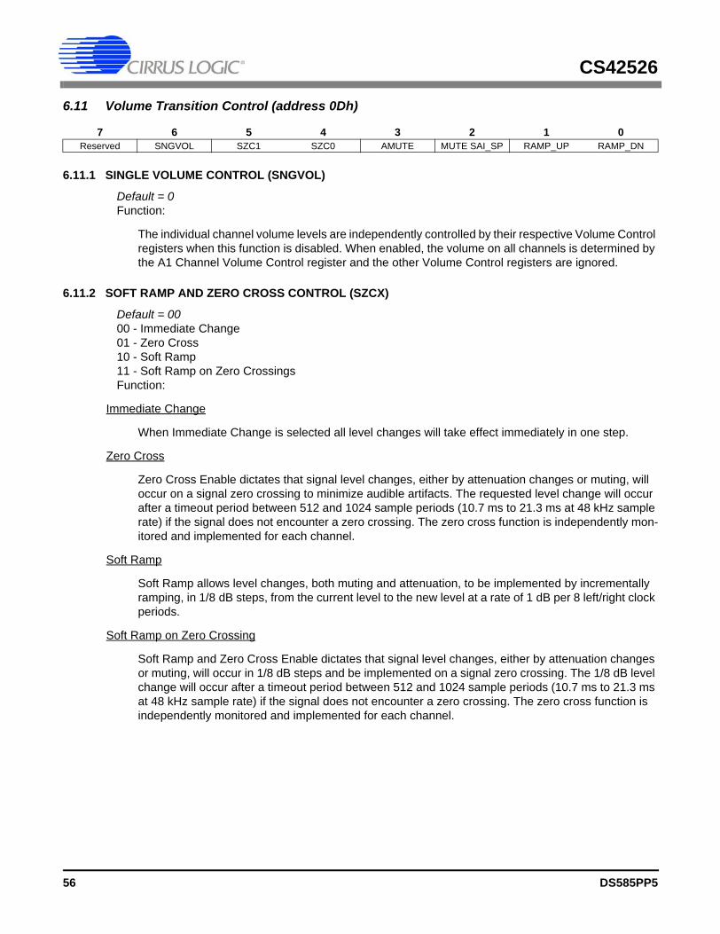
CS42526
6.11 Volume Transition Control (address 0Dh)
6.11.1 SINGLE VOLUME CONTROL (SNGVOL)
Default = 0Function:
The individual channel volume levels are independently controlled by their respective Volume Control registers when this function is disabled. When enabled, the volume on all channels is determined by the A1 Channel Volume Control register and the other Volume Control registers are ignored.
6.11.2 SOFT RAMP AND ZERO CROSS CONTROL (SZCX)
Default = 0000 - Immediate Change01 - Zero Cross 10 - Soft Ramp11 - Soft Ramp on Zero CrossingsFunction:
Immediate Change
When Immediate Change is selected all level changes will take effect immediately in one step.
Zero Cross
Zero Cross Enable dictates that signal level changes, either by attenuation changes or muting, will occur on a signal zero crossing to minimize audible artifacts. The requested level change will occur after a timeout period between 512 and 1024 sample periods (10.7 ms to 21.3 ms at 48 kHz sample rate) if the signal does not encounter a zero crossing. The zero cross function is independently mon-itored and implemented for each channel.
Soft Ramp
Soft Ramp allows level changes, both muting and attenuation, to be implemented by incrementally ramping, in 1/8 dB steps, from the current level to the new level at a rate of 1 dB per 8 left/right clock periods.
Soft Ramp on Zero Crossing
Soft Ramp and Zero Cross Enable dictates that signal level changes, either by attenuation changes or muting, will occur in 1/8 dB steps and be implemented on a signal zero crossing. The 1/8 dB level change will occur after a timeout period between 512 and 1024 sample periods (10.7 ms to 21.3 ms at 48 kHz sample rate) if the signal does not encounter a zero crossing. The zero cross function is independently monitored and implemented for each channel.
7 6 5 4 3 2 1 0Reserved SNGVOL SZC1 SZC0 AMUTE MUTE SAI_SP RAMP_UP RAMP_DN
56 DS585PP5
CS42526
6.11.3 AUTO-MUTE (AMUTE)
Default = 10 - Disabled1 - EnabledFunction:
The Digital-to-Analog converters of the CS42526 will mute the output following the reception of 8192 consecutive audio samples of static 0 or -1. A single sample of non-static data will release the mute. Detection and muting is done independently for each channel. The quiescent voltage on the output will be retained and the MUTEC pin will go active during the mute period. The muting function is af-fected, similar to volume control changes, by the Soft and Zero Cross bits (SZC[1:0]).
6.11.4 SERIAL AUDIO INTERFACE SERIAL PORT MUTE (MUTE SAI_SP)
Default = 00 - Disabled1 - EnabledFunction:
When enabled, the Serial Audio Interface port (SAI_SP) will be muted.
6.11.5 SOFT VOLUME RAMP-UP AFTER ERROR (RMP_UP)
Default = 00 - Disabled1 - EnabledFunction:
An un-mute will be performed after executing a filter mode change, after a MCLK/LRCK ratio change or error, and after changing the Functional Mode. When this feature is enabled, this un-mute is affect-ed, similar to attenuation changes, by the Soft and Zero Cross bits (SZC[1:0]). When disabled, an im-mediate un-mute is performed in these instances.
Note: For best results, it is recommended that this bit be used in conjunction with the RMP_DN bit.
6.11.6 SOFT RAMP-DOWN BEFORE FILTER MODE CHANGE (RMP_DN)
Default = 00 - Disabled1 - EnabledFunction:
A mute will be performed prior to executing a filter mode or de-emphasis mode change. When this feature is enabled, this mute is affected, similar to attenuation changes, by the Soft and Zero Cross bits (SZC[1:0]). When disabled, an immediate mute is performed prior to executing a filter mode or de-emphasis mode change.
Note: For best results, it is recommended that this bit be used in conjunction with the RMP_UP bit.
DS585PP5 57
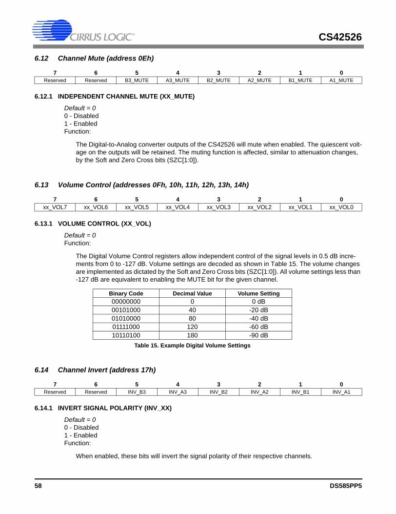
CS42526
6.12 Channel Mute (address 0Eh)
6.12.1 INDEPENDENT CHANNEL MUTE (XX_MUTE)
Default = 00 - Disabled1 - EnabledFunction:
The Digital-to-Analog converter outputs of the CS42526 will mute when enabled. The quiescent volt-age on the outputs will be retained. The muting function is affected, similar to attenuation changes, by the Soft and Zero Cross bits (SZC[1:0]).
6.13 Volume Control (addresses 0Fh, 10h, 11h, 12h, 13h, 14h)
6.13.1 VOLUME CONTROL (XX_VOL)
Default = 0Function:
The Digital Volume Control registers allow independent control of the signal levels in 0.5 dB incre-ments from 0 to -127 dB. Volume settings are decoded as shown in Table 15. The volume changes are implemented as dictated by the Soft and Zero Cross bits (SZC[1:0]). All volume settings less than -127 dB are equivalent to enabling the MUTE bit for the given channel.
6.14 Channel Invert (address 17h)
6.14.1 INVERT SIGNAL POLARITY (INV_XX)
Default = 00 - Disabled1 - EnabledFunction:
When enabled, these bits will invert the signal polarity of their respective channels.
7 6 5 4 3 2 1 0Reserved Reserved B3_MUTE A3_MUTE B2_MUTE A2_MUTE B1_MUTE A1_MUTE
7 6 5 4 3 2 1 0xx_VOL7 xx_VOL6 xx_VOL5 xx_VOL4 xx_VOL3 xx_VOL2 xx_VOL1 xx_VOL0
Binary Code Decimal Value Volume Setting00000000 0 0 dB00101000 40 -20 dB01010000 80 -40 dB01111000 120 -60 dB10110100 180 -90 dB
Table 15. Example Digital Volume Settings
7 6 5 4 3 2 1 0Reserved Reserved INV_B3 INV_A3 INV_B2 INV_A2 INV_B1 INV_A1
58 DS585PP5
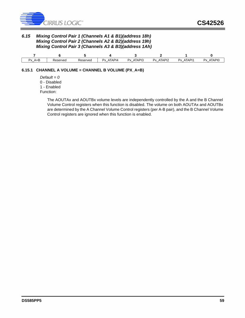
CS42526
6.15 Mixing Control Pair 1 (Channels A1 & B1)(address 18h)Mixing Control Pair 2 (Channels A2 & B2)(address 19h)Mixing Control Pair 3 (Channels A3 & B3)(address 1Ah)
6.15.1 CHANNEL A VOLUME = CHANNEL B VOLUME (PX_A=B)
Default = 00 - Disabled1 - EnabledFunction:
The AOUTAx and AOUTBx volume levels are independently controlled by the A and the B Channel Volume Control registers when this function is disabled. The volume on both AOUTAx and AOUTBx are determined by the A Channel Volume Control registers (per A-B pair), and the B Channel Volume Control registers are ignored when this function is enabled.
7 6 5 4 3 2 1 0Px_A=B Reserved Reserved Px_ATAPI4 Px_ATAPI3 Px_ATAPI2 Px_ATAPI1 Px_ATAPI0
DS585PP5 59
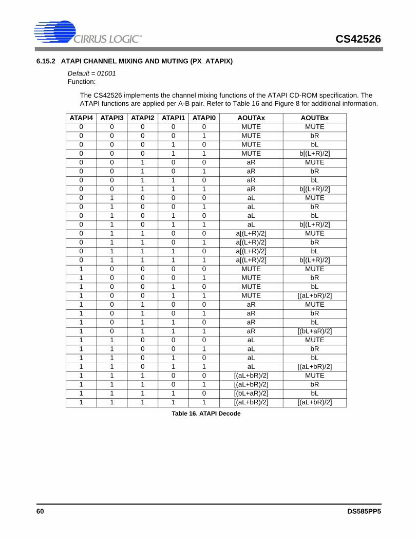
CS42526
6.15.2 ATAPI CHANNEL MIXING AND MUTING (PX_ATAPIX)
Default = 01001Function:
The CS42526 implements the channel mixing functions of the ATAPI CD-ROM specification. The ATAPI functions are applied per A-B pair. Refer to Table 16 and Figure 8 for additional information.
ATAPI4 ATAPI3 ATAPI2 ATAPI1 ATAPI0 AOUTAx AOUTBx0 0 0 0 0 MUTE MUTE0 0 0 0 1 MUTE bR0 0 0 1 0 MUTE bL0 0 0 1 1 MUTE b[(L+R)/2]0 0 1 0 0 aR MUTE0 0 1 0 1 aR bR0 0 1 1 0 aR bL0 0 1 1 1 aR b[(L+R)/2]0 1 0 0 0 aL MUTE0 1 0 0 1 aL bR0 1 0 1 0 aL bL0 1 0 1 1 aL b[(L+R)/2]0 1 1 0 0 a[(L+R)/2] MUTE0 1 1 0 1 a[(L+R)/2] bR0 1 1 1 0 a[(L+R)/2] bL0 1 1 1 1 a[(L+R)/2] b[(L+R)/2]1 0 0 0 0 MUTE MUTE1 0 0 0 1 MUTE bR1 0 0 1 0 MUTE bL1 0 0 1 1 MUTE [(aL+bR)/2]1 0 1 0 0 aR MUTE1 0 1 0 1 aR bR1 0 1 1 0 aR bL1 0 1 1 1 aR [(bL+aR)/2]1 1 0 0 0 aL MUTE1 1 0 0 1 aL bR1 1 0 1 0 aL bL1 1 0 1 1 aL [(aL+bR)/2]1 1 1 0 0 [(aL+bR)/2] MUTE1 1 1 0 1 [(aL+bR)/2] bR1 1 1 1 0 [(bL+aR)/2] bL1 1 1 1 1 [(aL+bR)/2] [(aL+bR)/2]
Table 16. ATAPI Decode
60 DS585PP5
CS42526
6.16 ADC Left Channel Gain (address 1Ch)
6.16.1 ADC LEFT CHANNEL GAIN (LGAINX)
Default = 00hFunction:
The level of the left analog channel can be adjusted in 1 dB increments as dictated by the Soft and Zero Cross bits (SZC[1:0]) from +15 to -15 dB. Levels are decoded in two’s complement, as shown in Table 17.
6.17 ADC Right Channel Gain (address 1Dh)
6.17.1 ADC RIGHT CHANNEL GAIN (RGAINX)
Default = 00hFunction:
The level of the right analog channel can be adjusted in 1 dB increments as dictated by the Soft and Zero Cross bits (SZC[1:0]) from +15 to -15 dB. Levels are decoded in two’s complement, as shown in Table 17.
6.18 Receiver Mode Control (address 1Eh)
6.18.1 SERIAL PORT SYNCHRONIZATION (SP_SYNC)
Default = 00 - CX & SAI Serial Port timings not in phase1 - CX & SAI Serial Port timings are in phaseFunction:
Forces the LRCK and SCLK from the CX & SAI Serial Ports to align and operate in phase. This func-tion will operate when both ports are running at the same sample rate or when operating at different sample rates.
7 6 5 4 3 2 1 0Reserved Reserved LGAIN5 LGAIN4 LGAIN3 LGAIN2 LGAIN1 LGAIN0
7 6 5 4 3 2 1 0Reserved Reserved RGAIN5 RGAIN4 RGAIN3 RGAIN2 RGAIN1 RGAIN0
Binary Code Decimal Value Volume Setting001111 +15 +15 dB001010 +10 +10 dB000101 +5 +5 dB000000 0 0 dB111011 -5 -5 dB110110 -10 -10 dB110001 -15 -15 dB
Table 17. Example ADC Input Gain Settings
7 6 5 4 3 2 1 0SP_SYNC Reserved DE-EMPH1 DE-EMPH0 INT1 INT0 HOLD1 HOLD0
DS585PP5 61
CS42526
6.18.2 DE-EMPHASIS SELECT BITS (DE-EMPHX)
Default = 0000 - Reserved01 - De-Emphasis for 32 kHz sample rate.10 - De-Emphasis for 44.1 kHz sample rate.11 - De-Emphasis for 48 kHz sample rate.Function:
Used to specify which de-emphasis filter to apply when the “Force PLL Lock (FRC_PLL_LK)” on page 53 is enabled.
6.18.3 INTERRUPT PIN CONTROL (INTX)
Default = 0000 - Active high; high output indicates interrupt condition has occurred01 - Active low, low output indicates an interrupt condition has occurred10 - Open drain, active low. Requires an external pull-up resistor on the INT pin.11 - ReservedFunction:
Determines how the interrupt pin (INT) will indicate an interrupt condition.
6.18.4 AUDIO SAMPLE HOLD (HOLDX)
Default = 0000 - Hold the last valid audio sample01 - Replace the current audio sample with 00 (mute)10 - Do not change the received audio sample11 - ReservedFunction:
Determines how received audio samples are affected when a receiver error occurs.
6.19 Receiver Mode Control 2 (address 1Fh)
6.19.1 TXP MULTIPLEXER (TMUXX)
Default = 000Function:
Selects which of the eight receiver inputs will be mapped directly to the TXP output pin.
7 6 5 4 3 2 1 0Reserved TMUX2 TMUX1 TMUX0 Reserved RMUX2 RMUX1 RMUX0
TMUX2 TMUX1 TMUX0 Description0 0 0 Output from pin RXP00 0 1 Output from pin RXP10 1 0 Output from pin RXP20 1 1 Output from pin RXP31 0 0 Output from pin RXP41 0 1 Output from pin RXP5
Table 18. TXP Output Selection
62 DS585PP5
CS42526
6.19.2 RECEIVER MULTIPLEXER (RMUXX)
Default = 000Function:
Selects which of the eight receiver inputs will be mapped to the internal receiver.
6.20 Interrupt Status (address 20h) (Read Only)
For all bits in this register, a “1” means the associated interrupt condition has occurred at least once since the register was last read. A ”0” means the associated interrupt condition has NOT occurred since the last reading of the register. Reading the register resets all bits to 0. Status bits that are masked off in the associated mask register will always be “0” in this register.
6.20.1 PLL UNLOCK (UNLOCK)
Default = 0Function:
PLL unlock status bit. This bit will go high if the PLL becomes unlocked.
6.20.2 NEW Q-SUBCODE BLOCK (QCH)
Default = 0Function:
Indicates when the Q-Subcode block has changed.
6.20.3 D TO E C-BUFFER TRANSFER (DETC)
Default = 0Function:
Indicates when the channel status buffer has changed.
1 1 0 Output from pin RXP61 1 1 Output from pin RXP7
RMUX2 RMUX1 RMUX0 Description0 0 0 Input from pin RXP00 0 1 Input from pin RXP10 1 0 Input from pin RXP20 1 1 Input from pin RXP31 0 0 Input from pin RXP41 0 1 Input from pin RXP51 1 0 Input from pin RXP61 1 1 Input from pin RXP7
Table 19. Receiver Input Selection
7 6 5 4 3 2 1 0UNLOCK Reserved QCH DETC DETU Reserved OverFlow RERR
TMUX2 TMUX1 TMUX0 Description
Table 18. TXP Output Selection
DS585PP5 63
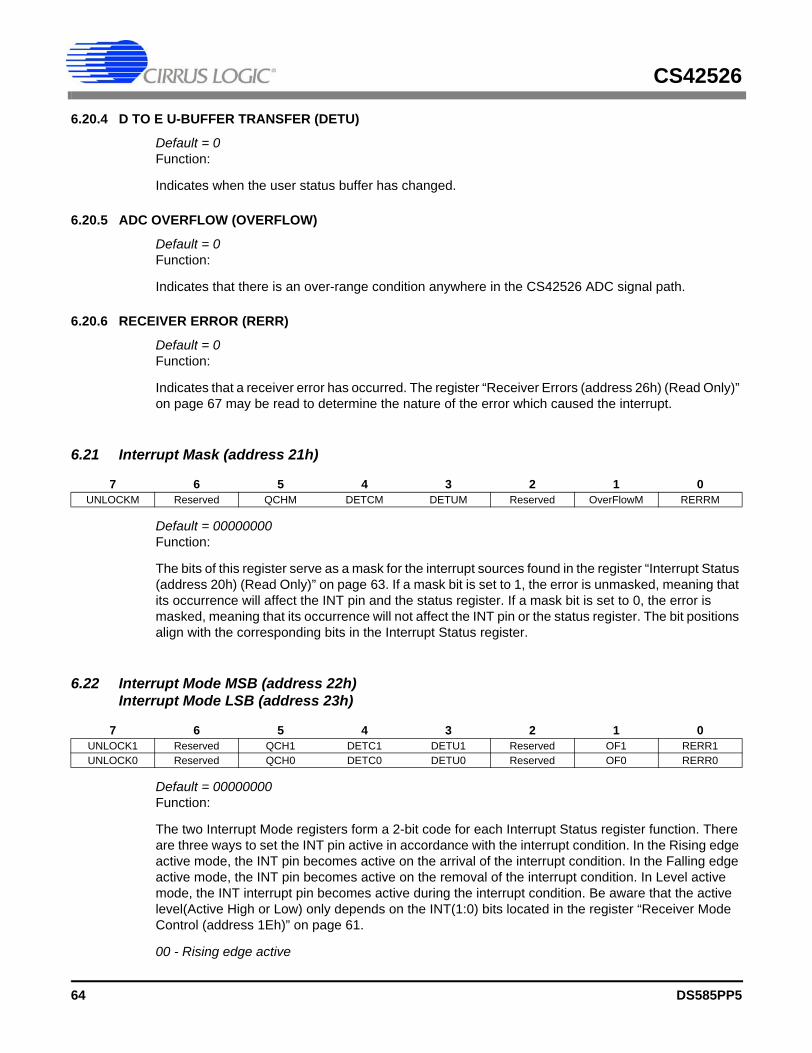
CS42526
6.20.4 D TO E U-BUFFER TRANSFER (DETU)
Default = 0Function:
Indicates when the user status buffer has changed.
6.20.5 ADC OVERFLOW (OVERFLOW)
Default = 0Function:
Indicates that there is an over-range condition anywhere in the CS42526 ADC signal path.
6.20.6 RECEIVER ERROR (RERR)
Default = 0Function:
Indicates that a receiver error has occurred. The register “Receiver Errors (address 26h) (Read Only)” on page 67 may be read to determine the nature of the error which caused the interrupt.
6.21 Interrupt Mask (address 21h)
Default = 00000000Function:
The bits of this register serve as a mask for the interrupt sources found in the register “Interrupt Status (address 20h) (Read Only)” on page 63. If a mask bit is set to 1, the error is unmasked, meaning that its occurrence will affect the INT pin and the status register. If a mask bit is set to 0, the error is masked, meaning that its occurrence will not affect the INT pin or the status register. The bit positions align with the corresponding bits in the Interrupt Status register.
6.22 Interrupt Mode MSB (address 22h)Interrupt Mode LSB (address 23h)
Default = 00000000Function:
The two Interrupt Mode registers form a 2-bit code for each Interrupt Status register function. There are three ways to set the INT pin active in accordance with the interrupt condition. In the Rising edge active mode, the INT pin becomes active on the arrival of the interrupt condition. In the Falling edge active mode, the INT pin becomes active on the removal of the interrupt condition. In Level active mode, the INT interrupt pin becomes active during the interrupt condition. Be aware that the active level(Active High or Low) only depends on the INT(1:0) bits located in the register “Receiver Mode Control (address 1Eh)” on page 61.
00 - Rising edge active
7 6 5 4 3 2 1 0UNLOCKM Reserved QCHM DETCM DETUM Reserved OverFlowM RERRM
7 6 5 4 3 2 1 0UNLOCK1 Reserved QCH1 DETC1 DETU1 Reserved OF1 RERR1UNLOCK0 Reserved QCH0 DETC0 DETU0 Reserved OF0 RERR0
64 DS585PP5
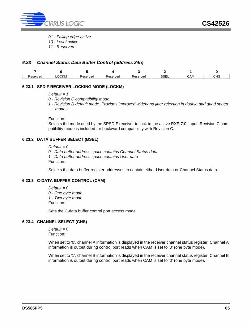
CS42526
01 - Falling edge active10 - Level active11 - Reserved
6.23 Channel Status Data Buffer Control (address 24h)
6.23.1 SPDIF RECEIVER LOCKING MODE (LOCKM)
Default = 10 - Revision C compatibility mode.1 - Revision D default mode. Provides improved wideband jitter rejection in double and quad speed
modes.
Function:Selects the mode used by the SPSDIF receiver to lock to the active RXP[7:0] input. Revision C com-patibility mode is included for backward compatibility with Revision C.
6.23.2 DATA BUFFER SELECT (BSEL)
Default = 00 - Data buffer address space contains Channel Status data1 - Data buffer address space contains User dataFunction:
Selects the data buffer register addresses to contain either User data or Channel Status data.
6.23.3 C-DATA BUFFER CONTROL (CAM)
Default = 00 - One byte mode1 - Two byte modeFunction:
Sets the C-data buffer control port access mode.
6.23.4 CHANNEL SELECT (CHS)
Default = 0Function:
When set to ‘0’, channel A information is displayed in the receiver channel status register. Channel A information is output during control port reads when CAM is set to ‘0’ (one byte mode).
When set to ‘1’, channel B information is displayed in the receiver channel status register. Channel B information is output during control port reads when CAM is set to ‘0’ (one byte mode).
7 6 5 4 3 2 1 0Reserved LOCKM Reserved Reserved Reserved BSEL CAM CHS
DS585PP5 65
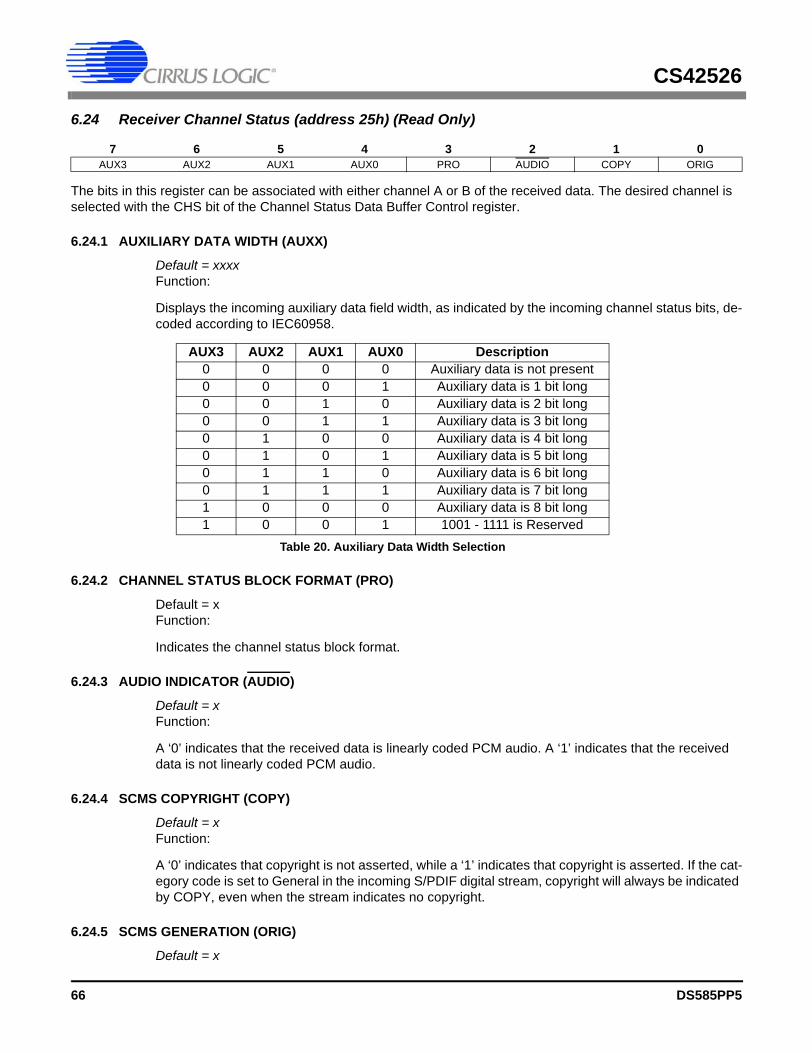
CS42526
6.24 Receiver Channel Status (address 25h) (Read Only)
The bits in this register can be associated with either channel A or B of the received data. The desired channel is selected with the CHS bit of the Channel Status Data Buffer Control register.
6.24.1 AUXILIARY DATA WIDTH (AUXX)
Default = xxxxFunction:
Displays the incoming auxiliary data field width, as indicated by the incoming channel status bits, de-coded according to IEC60958.
6.24.2 CHANNEL STATUS BLOCK FORMAT (PRO)
Default = xFunction:
Indicates the channel status block format.
6.24.3 AUDIO INDICATOR (AUDIO)
Default = xFunction:
A ‘0’ indicates that the received data is linearly coded PCM audio. A ‘1’ indicates that the received data is not linearly coded PCM audio.
6.24.4 SCMS COPYRIGHT (COPY)
Default = xFunction:
A ‘0’ indicates that copyright is not asserted, while a ‘1’ indicates that copyright is asserted. If the cat-egory code is set to General in the incoming S/PDIF digital stream, copyright will always be indicated by COPY, even when the stream indicates no copyright.
6.24.5 SCMS GENERATION (ORIG)
Default = x
7 6 5 4 3 2 1 0AUX3 AUX2 AUX1 AUX0 PRO AUDIO COPY ORIG
AUX3 AUX2 AUX1 AUX0 Description0 0 0 0 Auxiliary data is not present0 0 0 1 Auxiliary data is 1 bit long0 0 1 0 Auxiliary data is 2 bit long0 0 1 1 Auxiliary data is 3 bit long0 1 0 0 Auxiliary data is 4 bit long0 1 0 1 Auxiliary data is 5 bit long0 1 1 0 Auxiliary data is 6 bit long0 1 1 1 Auxiliary data is 7 bit long1 0 0 0 Auxiliary data is 8 bit long1 0 0 1 1001 - 1111 is Reserved
Table 20. Auxiliary Data Width Selection
66 DS585PP5
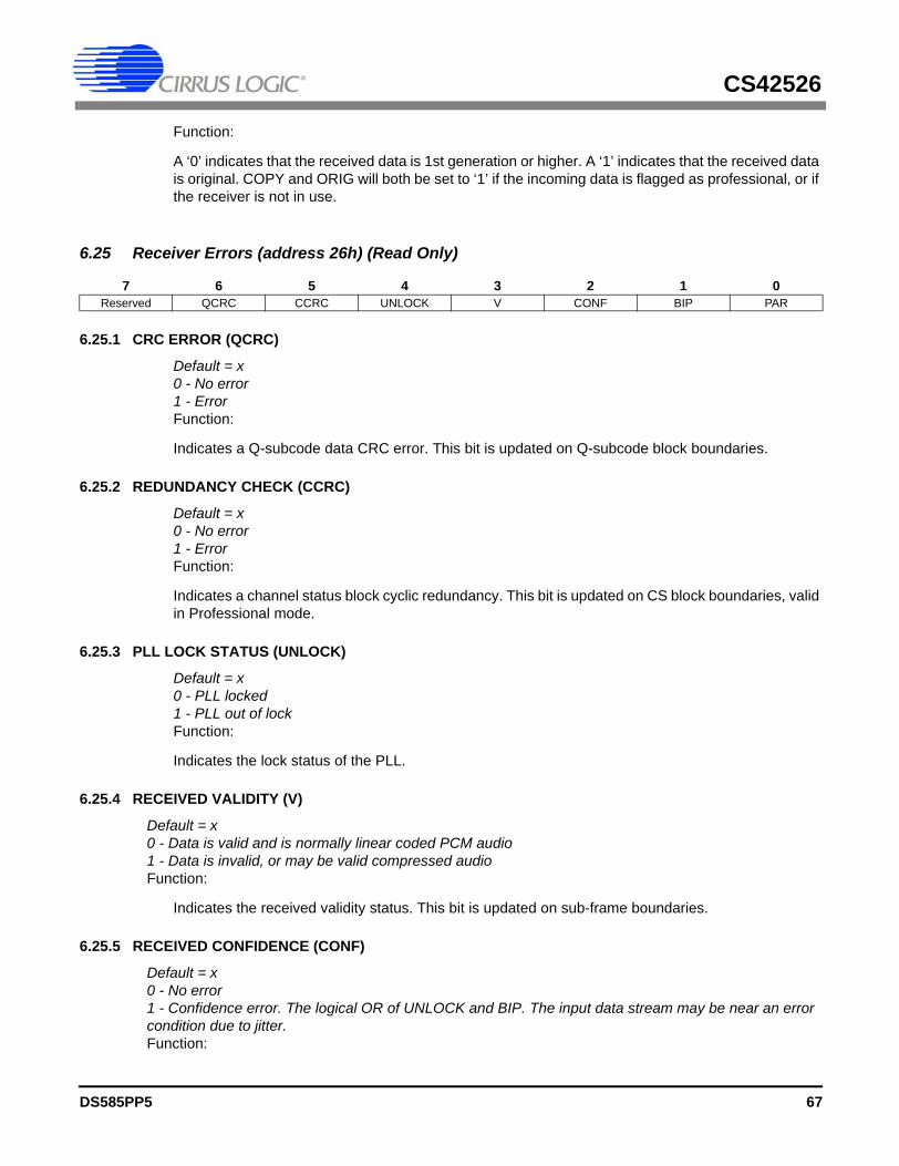
CS42526
Function:
A ‘0’ indicates that the received data is 1st generation or higher. A ‘1’ indicates that the received data is original. COPY and ORIG will both be set to ‘1’ if the incoming data is flagged as professional, or if the receiver is not in use.
6.25 Receiver Errors (address 26h) (Read Only)
6.25.1 CRC ERROR (QCRC)
Default = x0 - No error1 - ErrorFunction:
Indicates a Q-subcode data CRC error. This bit is updated on Q-subcode block boundaries.
6.25.2 REDUNDANCY CHECK (CCRC)
Default = x0 - No error1 - ErrorFunction:
Indicates a channel status block cyclic redundancy. This bit is updated on CS block boundaries, valid in Professional mode.
6.25.3 PLL LOCK STATUS (UNLOCK)
Default = x0 - PLL locked1 - PLL out of lockFunction:
Indicates the lock status of the PLL.
6.25.4 RECEIVED VALIDITY (V)
Default = x0 - Data is valid and is normally linear coded PCM audio1 - Data is invalid, or may be valid compressed audioFunction:
Indicates the received validity status. This bit is updated on sub-frame boundaries.
6.25.5 RECEIVED CONFIDENCE (CONF)
Default = x0 - No error1 - Confidence error. The logical OR of UNLOCK and BIP. The input data stream may be near an error condition due to jitter.Function:
7 6 5 4 3 2 1 0Reserved QCRC CCRC UNLOCK V CONF BIP PAR
DS585PP5 67
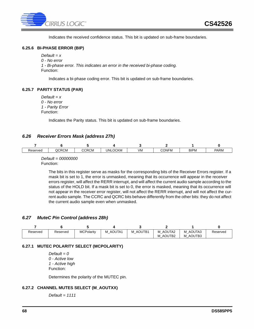
CS42526
Indicates the received confidence status. This bit is updated on sub-frame boundaries.
6.25.6 BI-PHASE ERROR (BIP)
Default = x0 - No error1 - Bi-phase error. This indicates an error in the received bi-phase coding.Function:
Indicates a bi-phase coding error. This bit is updated on sub-frame boundaries.
6.25.7 PARITY STATUS (PAR)
Default = x0 - No error1 - Parity ErrorFunction:
Indicates the Parity status. This bit is updated on sub-frame boundaries.
6.26 Receiver Errors Mask (address 27h)
Default = 00000000Function:
The bits in this register serve as masks for the corresponding bits of the Receiver Errors register. If a mask bit is set to 1, the error is unmasked, meaning that its occurrence will appear in the receiver errors register, will affect the RERR interrupt, and will affect the current audio sample according to the status of the HOLD bit. If a mask bit is set to 0, the error is masked, meaning that its occurrence will not appear in the receiver error register, will not affect the RERR interrupt, and will not affect the cur-rent audio sample. The CCRC and QCRC bits behave differently from the other bits: they do not affect the current audio sample even when unmasked.
6.27 MuteC Pin Control (address 28h)
6.27.1 MUTEC POLARITY SELECT (MCPOLARITY)
Default = 00 - Active low1 - Active highFunction:
Determines the polarity of the MUTEC pin.
6.27.2 CHANNEL MUTES SELECT (M_AOUTXX)
Default = 1111
7 6 5 4 3 2 1 0Reserved QCRCM CCRCM UNLOCKM VM CONFM BIPM PARM
7 6 5 4 3 2 1 0Reserved Reserved MCPolarity M_AOUTA1 M_AOUTB1 M_AOUTA2
M_AOUTB2M_AOUTA3M_AOUTB3
Reserved
68 DS585PP5
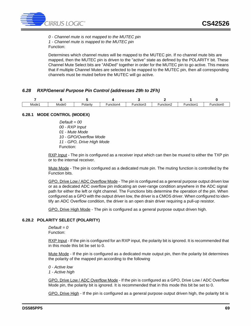
CS42526
0 - Channel mute is not mapped to the MUTEC pin1 - Channel mute is mapped to the MUTEC pinFunction:
Determines which channel mutes will be mapped to the MUTEC pin. If no channel mute bits are mapped, then the MUTEC pin is driven to the "active" state as defined by the POLARITY bit. These Channel Mute Select bits are "ANDed" together in order for the MUTEC pin to go active. This means that if multiple Channel Mutes are selected to be mapped to the MUTEC pin, then all corresponding channels must be muted before the MUTEC will go active.
6.28 RXP/General Purpose Pin Control (addresses 29h to 2Fh)
6.28.1 MODE CONTROL (MODEX)
Default = 0000 - RXP Input01 - Mute Mode10 - GPO/Overflow Mode11 - GPO, Drive High ModeFunction:
RXP Input - The pin is configured as a receiver input which can then be muxed to either the TXP pin or to the internal receiver.
Mute Mode - The pin is configured as a dedicated mute pin. The muting function is controlled by the Function bits.
GPO, Drive Low / ADC Overflow Mode - The pin is configured as a general purpose output driven low or as a dedicated ADC overflow pin indicating an over-range condition anywhere in the ADC signal path for either the left or right channel. The Functionx bits determine the operation of the pin. When configured as a GPO with the output driven low, the driver is a CMOS driver. When configured to iden-tify an ADC Overflow condition, the driver is an open drain driver requiring a pull-up resistor.
GPO, Drive High Mode - The pin is configured as a general purpose output driven high.
6.28.2 POLARITY SELECT (POLARITY)
Default = 0Function:
RXP Input - If the pin is configured for an RXP input, the polarity bit is ignored. It is recommended that in this mode this bit be set to 0.
Mute Mode - If the pin is configured as a dedicated mute output pin, then the polarity bit determines the polarity of the mapped pin according to the following
0 - Active low1 - Active high
GPO, Drive Low / ADC Overflow Mode - If the pin is configured as a GPO, Drive Low / ADC Overflow Mode pin, the polarity bit is ignored. It is recommended that in this mode this bit be set to 0.
GPO, Drive High - If the pin is configured as a general purpose output driven high, the polarity bit is
7 6 5 4 3 2 1 0Mode1 Mode0 Polarity Function4 Function3 Function2 Function1 Function0
DS585PP5 69
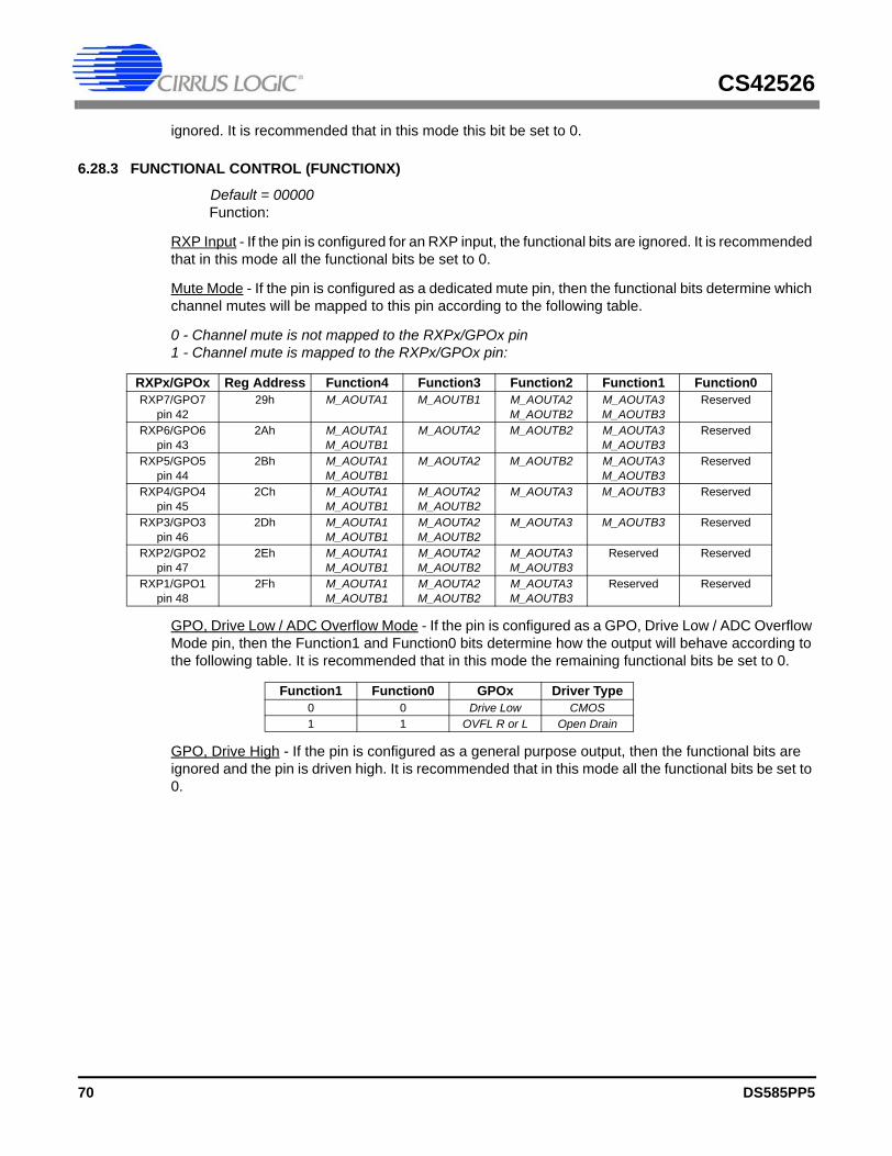
CS42526
ignored. It is recommended that in this mode this bit be set to 0.
6.28.3 FUNCTIONAL CONTROL (FUNCTIONX)
Default = 00000Function:
RXP Input - If the pin is configured for an RXP input, the functional bits are ignored. It is recommended that in this mode all the functional bits be set to 0.
Mute Mode - If the pin is configured as a dedicated mute pin, then the functional bits determine which channel mutes will be mapped to this pin according to the following table.
0 - Channel mute is not mapped to the RXPx/GPOx pin1 - Channel mute is mapped to the RXPx/GPOx pin:
GPO, Drive Low / ADC Overflow Mode - If the pin is configured as a GPO, Drive Low / ADC Overflow Mode pin, then the Function1 and Function0 bits determine how the output will behave according to the following table. It is recommended that in this mode the remaining functional bits be set to 0.
GPO, Drive High - If the pin is configured as a general purpose output, then the functional bits are ignored and the pin is driven high. It is recommended that in this mode all the functional bits be set to 0.
RXPx/GPOx Reg Address Function4 Function3 Function2 Function1 Function0RXP7/GPO7
pin 4229h M_AOUTA1 M_AOUTB1 M_AOUTA2
M_AOUTB2M_AOUTA3M_AOUTB3
Reserved
RXP6/GPO6pin 43
2Ah M_AOUTA1M_AOUTB1
M_AOUTA2 M_AOUTB2 M_AOUTA3M_AOUTB3
Reserved
RXP5/GPO5pin 44
2Bh M_AOUTA1M_AOUTB1
M_AOUTA2 M_AOUTB2 M_AOUTA3M_AOUTB3
Reserved
RXP4/GPO4pin 45
2Ch M_AOUTA1M_AOUTB1
M_AOUTA2M_AOUTB2
M_AOUTA3 M_AOUTB3 Reserved
RXP3/GPO3pin 46
2Dh M_AOUTA1M_AOUTB1
M_AOUTA2M_AOUTB2
M_AOUTA3 M_AOUTB3 Reserved
RXP2/GPO2pin 47
2Eh M_AOUTA1M_AOUTB1
M_AOUTA2M_AOUTB2
M_AOUTA3M_AOUTB3
Reserved Reserved
RXP1/GPO1pin 48
2Fh M_AOUTA1M_AOUTB1
M_AOUTA2M_AOUTB2
M_AOUTA3M_AOUTB3
Reserved Reserved
Function1 Function0 GPOx Driver Type0 0 Drive Low CMOS1 1 OVFL R or L Open Drain
70 DS585PP5
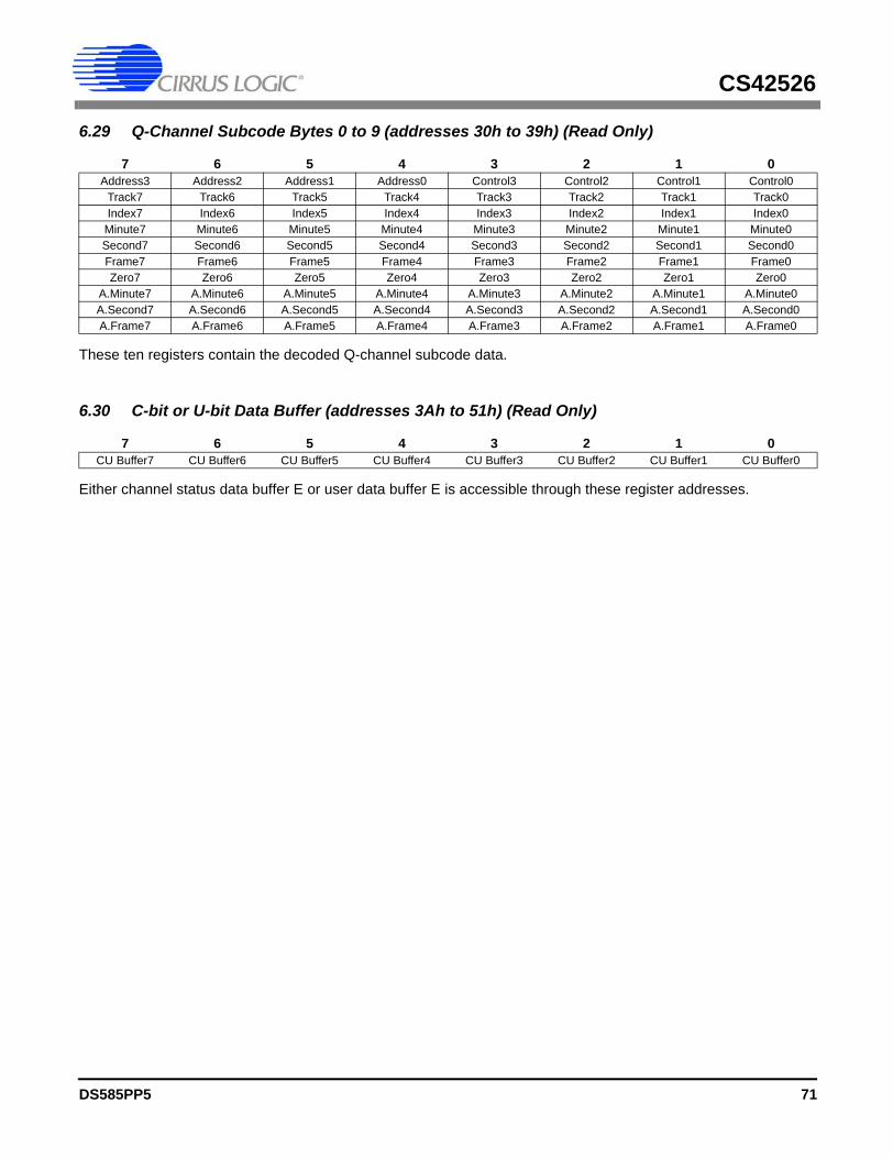
CS42526
6.29 Q-Channel Subcode Bytes 0 to 9 (addresses 30h to 39h) (Read Only)
These ten registers contain the decoded Q-channel subcode data.
6.30 C-bit or U-bit Data Buffer (addresses 3Ah to 51h) (Read Only)
Either channel status data buffer E or user data buffer E is accessible through these register addresses.
7 6 5 4 3 2 1 0Address3 Address2 Address1 Address0 Control3 Control2 Control1 Control0
Track7 Track6 Track5 Track4 Track3 Track2 Track1 Track0Index7 Index6 Index5 Index4 Index3 Index2 Index1 Index0Minute7 Minute6 Minute5 Minute4 Minute3 Minute2 Minute1 Minute0Second7 Second6 Second5 Second4 Second3 Second2 Second1 Second0Frame7 Frame6 Frame5 Frame4 Frame3 Frame2 Frame1 Frame0Zero7 Zero6 Zero5 Zero4 Zero3 Zero2 Zero1 Zero0
A.Minute7 A.Minute6 A.Minute5 A.Minute4 A.Minute3 A.Minute2 A.Minute1 A.Minute0A.Second7 A.Second6 A.Second5 A.Second4 A.Second3 A.Second2 A.Second1 A.Second0A.Frame7 A.Frame6 A.Frame5 A.Frame4 A.Frame3 A.Frame2 A.Frame1 A.Frame0
7 6 5 4 3 2 1 0CU Buffer7 CU Buffer6 CU Buffer5 CU Buffer4 CU Buffer3 CU Buffer2 CU Buffer1 CU Buffer0
DS585PP5 71
CS42526
7. PARAMETER DEFINITIONSDynamic Range
The ratio of the rms value of the signal to the rms sum of all other spectral components over the specified bandwidth. Dynamic Range is a signal-to-noise ratio measurement over the specified band width made with a -60 dBFS signal. 60 dB is added to resulting measurement to refer the measurement to full-scale. This technique ensures that the distortion components are below the noise level and do not effect the measurement. This measurement technique has been accepted by the Audio Engineering Society, AES17-1991, and the Electronic Industries Association of Japan, EIAJ CP-307. Expressed in decibels.
Total Harmonic Distortion + NoiseThe ratio of the rms value of the signal to the rms sum of all other spectral components over the specified band width (typically 10 Hz to 20 kHz), including distortion components. Expressed in decibels. Measured at -1 and -20 dBFS as suggested in AES17-1991 Annex A.
Frequency ResponseA measure of the amplitude response variation from 10 Hz to 20 kHz relative to the amplitude response at 1 kHz. Units in decibels.
Interchannel IsolationA measure of crosstalk between the left and right channels. Measured for each channel at the converter's output with no signal to the input under test and a full-scale signal applied to the other channel. Units in decibels.
Interchannel Gain MismatchThe gain difference between left and right channels. Units in decibels.
Gain ErrorThe deviation from the nominal full-scale analog output for a full-scale digital input.
Gain DriftThe change in gain value with temperature. Units in ppm/°C.
Offset ErrorThe deviation of the mid-scale transition (111...111 to 000...000) from the ideal. Units in mV.
72 DS585PP5
CS42526
8. REFERENCES1) Cirrus Logic, Audio Quality Measurement Specification, Version 1.0, 1997.
http://www.cirrus.com/products/papers/meas/meas.html2) Cirrus Logic, AN18: Layout and Design Rules for Data Converters and Other Mixed Signal Devices,
Version 6.0, February 1998.3) Cirrus Logic, AN22: Overview of Digital Audio Interface Data Structures, Version 2.0, February 1998.;
A useful tutorial on digital audio specifications. 4) Cirrus Logic, AN134: AES and S/PDIF Recommended Transformers, Version 2, April 1999.5) Cirrus Logic, An Understanding and Implementation of the SCMS Serial Copy Management System
for Digital Audio Transmission, by Clifton Sanchez.; an excellent tutorial on SCMS. It is available fromthe AES as preprint 3518.
6) Cirrus Logic, Techniques to Measure and Maximize the Performance of a 120 dB, 96 kHz A/D Con-verter Integrated Circuit, by Steven Harris, Steven Green and Ka Leung. Presented at the 103rd Con-vention of the Audio Engineering Society, September 1997.
7) Cirrus Logic, A Stereo 16-bit Delta-Sigma A/D Converter for Digital Audio, by D.R. Welland, B.P. DelSignore, E.J. Swanson, T. Tanaka, K. Hamashita, S. Hara, K. Takasuka. Paper presented at the 85thConvention of the Audio Engineering Society, November 1988.
8) Cirrus Logic, The Effects of Sampling Clock Jitter on Nyquist Sampling Analog-to-Digital Converters,and on Oversampling Delta Sigma ADC's, by Steven Harris. Paper presented at the 87th Conventionof the Audio Engineering Society, October 1989.
9) Cirrus Logic, An 18-Bit Dual-Channel Oversampling Delta-Sigma A/D Converter, with 19-Bit Mono Ap-plication Example, by Clif Sanchez. Paper presented at the 87th Convention of the Audio EngineeringSociety, October 1989.
10) Cirrus Logic, How to Achieve Optimum Performance from Delta-Sigma A/D and D/A Converters,bySteven Harris. Presented at the 93rd Convention of the Audio Engineering Society, October 1992.
11) Cirrus Logic, A Fifth-Order Delta-Sigma Modulator with 110 dB Audio Dynamic Range, by I. Fujimori,K. Hamashita and E.J. Swanson. Paper presented at the 93rd Convention of the Audio EngineeringSociety, October 1992.
12) International Electrotechnical Commission, IEC60958, http://www.ansi.org13) Philips Semiconductor, The I2C-Bus Specification: Version 2.1, January 2000. http://www.semicon-
ductors.philips.com
DS585PP5 73
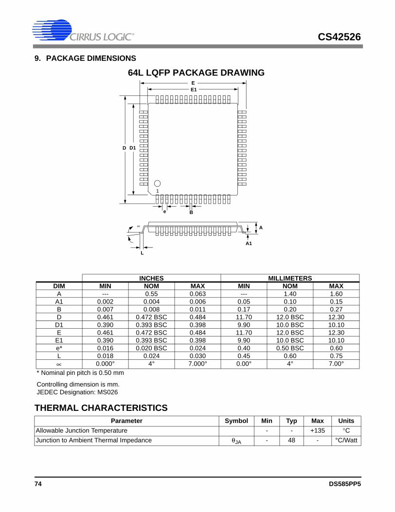
CS42526
9. PACKAGE DIMENSIONS
THERMAL CHARACTERISTICS
INCHES MILLIMETERSDIM MIN NOM MAX MIN NOM MAX
A --- 0.55 0.063 --- 1.40 1.60A1 0.002 0.004 0.006 0.05 0.10 0.15B 0.007 0.008 0.011 0.17 0.20 0.27D 0.461 0.472 BSC 0.484 11.70 12.0 BSC 12.30
D1 0.390 0.393 BSC 0.398 9.90 10.0 BSC 10.10E 0.461 0.472 BSC 0.484 11.70 12.0 BSC 12.30E1 0.390 0.393 BSC 0.398 9.90 10.0 BSC 10.10e* 0.016 0.020 BSC 0.024 0.40 0.50 BSC 0.60L 0.018 0.024 0.030 0.45 0.60 0.75∝ 0.000° 4° 7.000° 0.00° 4° 7.00°
* Nominal pin pitch is 0.50 mm
Controlling dimension is mm.JEDEC Designation: MS026
Parameter Symbol Min Typ Max UnitsAllowable Junction Temperature - - +135 °CJunction to Ambient Thermal Impedance θJA - 48 - °C/Watt
64L LQFP PACKAGE DRAWINGE1E
D1D
1
e
L
∝
B
A1
A
74 DS585PP5
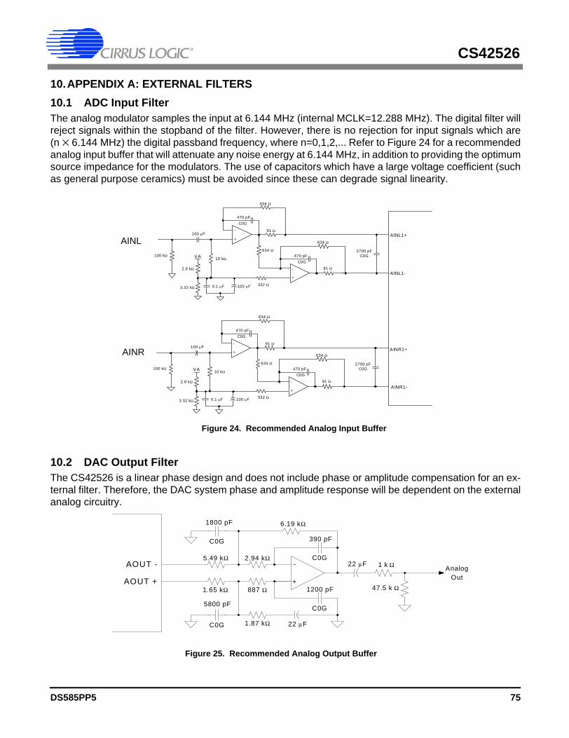
CS42526
10.APPENDIX A: EXTERNAL FILTERS10.1 ADC Input FilterThe analog modulator samples the input at 6.144 MHz (internal MCLK=12.288 MHz). The digital filter willreject signals within the stopband of the filter. However, there is no rejection for input signals which are(n × 6.144 MHz) the digital passband frequency, where n=0,1,2,... Refer to Figure 24 for a recommendedanalog input buffer that will attenuate any noise energy at 6.144 MHz, in addition to providing the optimumsource impedance for the modulators. The use of capacitors which have a large voltage coefficient (suchas general purpose ceramics) must be avoided since these can degrade signal linearity.
10.2 DAC Output FilterThe CS42526 is a linear phase design and does not include phase or amplitude compensation for an ex-ternal filter. Therefore, the DAC system phase and amplitude response will be dependent on the externalanalog circuitry.
VA
+
+
-
-100 µF
100 kΩ10 kΩ
3.32 kΩ
2.8 kΩ
0.1 µF 100 µF
470 pF
470 pFC0G
C0G
634 Ω
634 Ω
634 Ω
91 Ω
91 Ω
2700 pFC0G
AINL1+
AINL1-
AINR1+
AINR1-
VA
+
+
-
-100 µF
100 kΩ10 kΩ
3.32 kΩ
2.8 kΩ
0.1 µF 100 µF
470 pF
470 pFC0G
C0G
634 Ω
634 Ω
634 Ω
91 Ω
91 Ω
2700 pFC0G
332 Ω
332 Ω
Figure 24. Recommended Analog Input Buffer
AINL
AINR
AOUT +
AOUT - -
+
390 pF
C0G1 k Ω22 µF
6.19 kΩ1800 pF
C0G
887 Ω
2.94 kΩ5.49 kΩ
1.65 kΩ
1.87 kΩ 22 µF
1200 pF
C0G5800 pF
C0G
47.5 k Ω
AnalogOut
Figure 25. Recommended Analog Output Buffer
DS585PP5 75
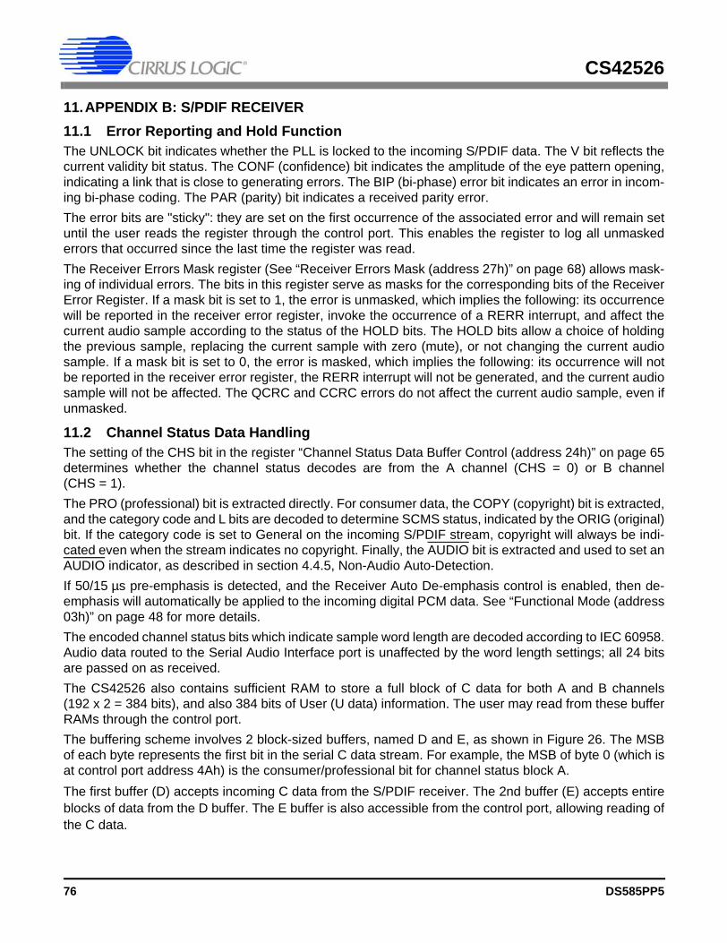
CS42526
11.APPENDIX B: S/PDIF RECEIVER11.1 Error Reporting and Hold FunctionThe UNLOCK bit indicates whether the PLL is locked to the incoming S/PDIF data. The V bit reflects thecurrent validity bit status. The CONF (confidence) bit indicates the amplitude of the eye pattern opening,indicating a link that is close to generating errors. The BIP (bi-phase) error bit indicates an error in incom-ing bi-phase coding. The PAR (parity) bit indicates a received parity error. The error bits are "sticky": they are set on the first occurrence of the associated error and will remain setuntil the user reads the register through the control port. This enables the register to log all unmaskederrors that occurred since the last time the register was read.The Receiver Errors Mask register (See “Receiver Errors Mask (address 27h)” on page 68) allows mask-ing of individual errors. The bits in this register serve as masks for the corresponding bits of the ReceiverError Register. If a mask bit is set to 1, the error is unmasked, which implies the following: its occurrencewill be reported in the receiver error register, invoke the occurrence of a RERR interrupt, and affect thecurrent audio sample according to the status of the HOLD bits. The HOLD bits allow a choice of holdingthe previous sample, replacing the current sample with zero (mute), or not changing the current audiosample. If a mask bit is set to 0, the error is masked, which implies the following: its occurrence will notbe reported in the receiver error register, the RERR interrupt will not be generated, and the current audiosample will not be affected. The QCRC and CCRC errors do not affect the current audio sample, even ifunmasked.
11.2 Channel Status Data HandlingThe setting of the CHS bit in the register “Channel Status Data Buffer Control (address 24h)” on page 65determines whether the channel status decodes are from the A channel (CHS = 0) or B channel(CHS = 1).The PRO (professional) bit is extracted directly. For consumer data, the COPY (copyright) bit is extracted,and the category code and L bits are decoded to determine SCMS status, indicated by the ORIG (original)bit. If the category code is set to General on the incoming S/PDIF stream, copyright will always be indi-cated even when the stream indicates no copyright. Finally, the AUDIO bit is extracted and used to set anAUDIO indicator, as described in section 4.4.5, Non-Audio Auto-Detection.If 50/15 µs pre-emphasis is detected, and the Receiver Auto De-emphasis control is enabled, then de-emphasis will automatically be applied to the incoming digital PCM data. See “Functional Mode (address03h)” on page 48 for more details.The encoded channel status bits which indicate sample word length are decoded according to IEC 60958.Audio data routed to the Serial Audio Interface port is unaffected by the word length settings; all 24 bitsare passed on as received.The CS42526 also contains sufficient RAM to store a full block of C data for both A and B channels(192 x 2 = 384 bits), and also 384 bits of User (U data) information. The user may read from these bufferRAMs through the control port.The buffering scheme involves 2 block-sized buffers, named D and E, as shown in Figure 26. The MSBof each byte represents the first bit in the serial C data stream. For example, the MSB of byte 0 (which isat control port address 4Ah) is the consumer/professional bit for channel status block A. The first buffer (D) accepts incoming C data from the S/PDIF receiver. The 2nd buffer (E) accepts entireblocks of data from the D buffer. The E buffer is also accessible from the control port, allowing reading ofthe C data.
76 DS585PP5
CS42526
11.2.1 Channel Status Data E Buffer AccessThe user can monitor the incoming Channel Status data by reading the E buffer, which is mapped into theregister space of the CS42526, through the control port Data Buffer. The Data Buffer must first be config-ured to point to the address space of the C data. This is accomplished by setting the BSEL bit to ‘0’ in theregister “Channel Status Data Buffer Control (address 24h)” on page 65.The user can configure the Interrupt Mask Register to cause an interrupt whenever any data bit changesare detected when D to E Channel Status buffer transfers occur. If no data bits have changed within thecurrent transfer of data from D to E, then no interrupt will be generated. This allows determination of theacceptable time periods to interact with the E buffer. See “Interrupt Mask (address 21h)” on page 64 formore details.The E buffer is organized as 24 x 16-bit words. For each word the MS Byte is the A channel data, and theLS Byte is the B channel data (see Figure 26). There are two methods of accessing this memory, knownas one byte mode and two byte mode. The desired mode is selected by setting the CAM bit in the ChannelStatus Data Buffer Control Register.
11.2.1a One Byte modeIn many applications, the channel status blocks for the A and B channels will be identical. In this situation,the user may read a byte from one of the channel's blocks since the corresponding byte for the other chan-nel will likely be the same. One byte mode takes advantage of the often identical nature of A and B chan-nel status data. When reading data in one byte mode, a single byte is returned, which can be from channelA or B data, depending on a register control bit.One byte mode saves the user substantial control port access time, as it effectively accesses 2 bytesworth of information in 1 byte's worth of access time. If the control port's autoincrement addressing is usedin combination with this mode, multi-byte accesses such as full-block reads can be done especially effi-ciently.
11.2.1b Two Byte modeThere are those applications in which the A and B channel status blocks will not be the same, and theuser is interested in accessing both blocks. In these situations, two byte mode should be used to accessthe E buffer. In this mode, a read will cause the CS42526 to output two bytes from its control port. The first byte out willrepresent the A channel status data, and the second byte will represent the B channel status data.
Control Port
FromS/PDIF
Receiver
E
24words
8-bits 8-bitsA B
D
ReceivedDataBuffer
Figure 26. Channel Status Data Buffer Structure
DS585PP5 77
CS42526
11.2.2 Serial Copy Management System (SCMS)The CS42526 allows read access to all the channel status bits. For consumer mode SCMS compliance,the host microcontroller needs to read and interpret the Category Code, Copy bit and L bit appropriately.
11.3 User (U) Data E Buffer AccessEntire blocks of U data are buffered using a cascade of 2 block-sized RAMs to perform the buffering asdescribed in the Channel Status section. The user has access to the E buffer through the control port DataBuffer which is mapped into the register space of the CS42526. The Data Buffer must first be configuredto point to the address space of the U data. This is accomplished by setting the BSEL bit to ‘1’ in the reg-ister “Channel Status Data Buffer Control (address 24h)” on page 65.The user can configure the Interrupt Mask Register to cause an interrupt whenever any data bit changesare detected when D to E Channel Status buffer transfers occur. If no data bits have changed within thecurrent transfer of data from D to E, then no interrupt will be generated. This allows determination of theacceptable time periods to interact with the E buffer. See “Interrupt Mask (address 21h)” on page 64 formore details.The U buffer access only operates in two byte mode, since there is no concept of A and B blocks for userdata. The arrangement of the data is as follows: Bit15[A7]Bit14[B7]Bit13[A6]Bit12[B6]...Bit1[A0]Bit0[B0].The arrangement of the data in each byte is as follows: MSB is the first received bit and is the first trans-mitted bit. The first byte read is the first byte received, and the first byte sent is the first byte transmitted.When two bytes are read from the E buffer, the bits are presented in the following arrangement:A[7]B[7]A[6]B[6]....A[0]B[0].
11.3.1 Non-Audio Auto-DetectionThe CS42526 S/PDIF receiver can detect non-audio data originating from AC-3® or MPEG encoders.This is accomplished by looking for a 96-bit sync code, consisting of 0x0000, 0x0000, 0x0000, 0x0000,0xF872, and 0x4E1F. When the sync code is detected, an internal AUTODETECT signal will be asserted.If no additional sync codes are detected within the next 4096 frames, AUTODETECT will be de-asserteduntil another sync code is detected. The AUDIO bit in the Receiver Channel Status register is the logicalOR of AUTODETECT and the received channel status bit 1. If non-audio data is detected, the data will beprocessed exactly as if it were normal audio. It is up to the user to mute the outputs as required.
11.3.1a Format DetectionThe CS42526 can automatically detect various serial audio input formats. The Receiver Status register(08h) is used to indicate a detected format. The register will indicate if uncompressed PCM data,IEC61937 data, DTS-LD data, DTS-CD data, or digital silence was detected. Additionally, the IEC61937Pc/Pd burst preambles are available in registers 09h-0Ch. See the register descriptions for more informa-tion.
78 DS585PP5
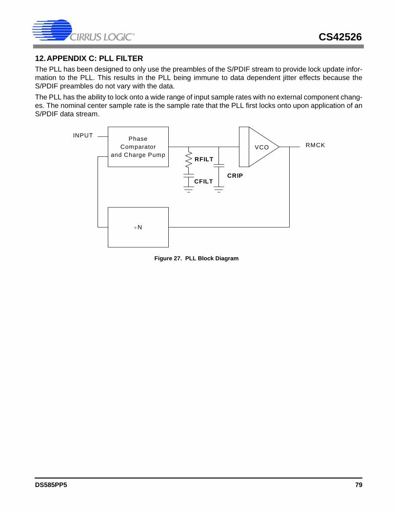
CS42526
12.APPENDIX C: PLL FILTERThe PLL has been designed to only use the preambles of the S/PDIF stream to provide lock update infor-mation to the PLL. This results in the PLL being immune to data dependent jitter effects because theS/PDIF preambles do not vary with the data.The PLL has the ability to lock onto a wide range of input sample rates with no external component chang-es. The nominal center sample rate is the sample rate that the PLL first locks onto upon application of anS/PDIF data stream.
PhaseComparator
and Charge Pump
÷N
VCO RMCKINPUT
CRIPCFILT
RFILT
Figure 27. PLL Block Diagram
DS585PP5 79
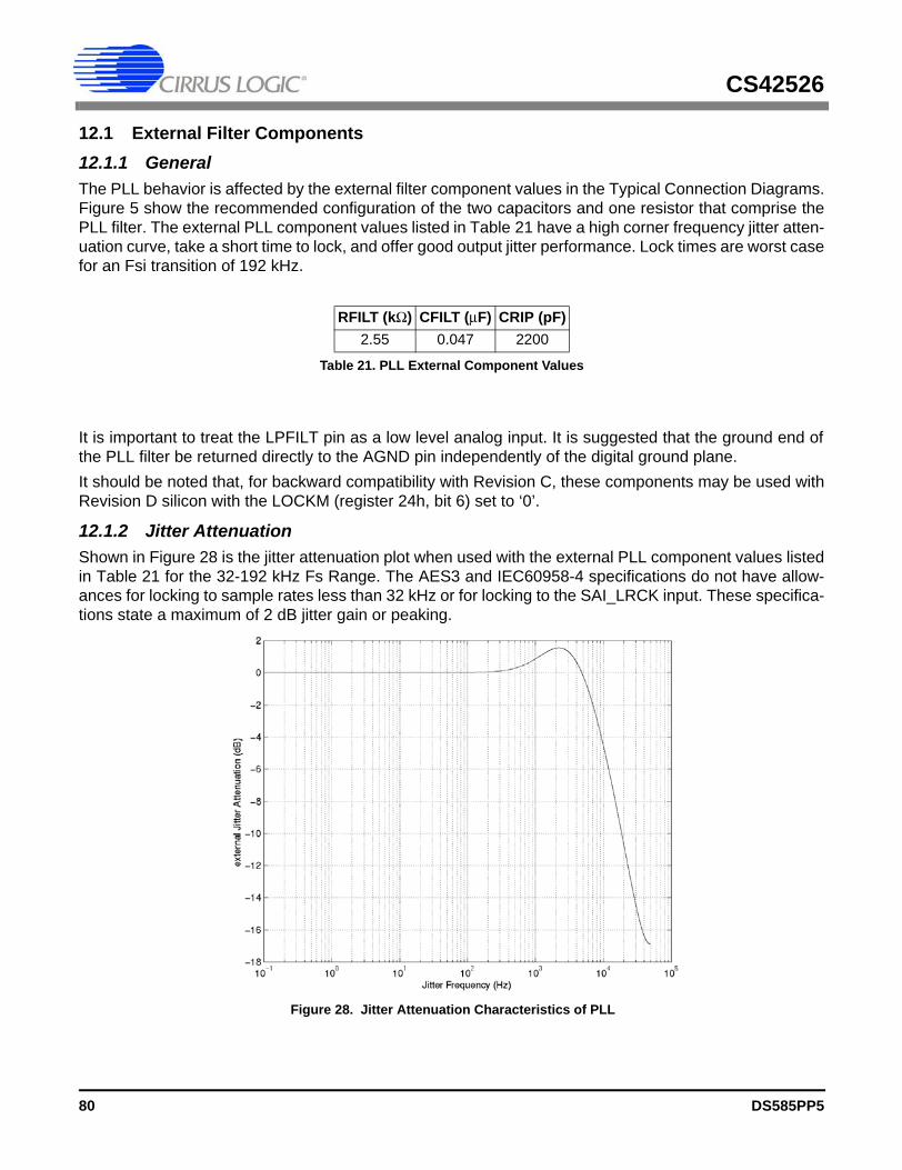
CS42526
12.1 External Filter Components12.1.1 GeneralThe PLL behavior is affected by the external filter component values in the Typical Connection Diagrams.Figure 5 show the recommended configuration of the two capacitors and one resistor that comprise thePLL filter. The external PLL component values listed in Table 21 have a high corner frequency jitter atten-uation curve, take a short time to lock, and offer good output jitter performance. Lock times are worst casefor an Fsi transition of 192 kHz.
It is important to treat the LPFILT pin as a low level analog input. It is suggested that the ground end ofthe PLL filter be returned directly to the AGND pin independently of the digital ground plane.It should be noted that, for backward compatibility with Revision C, these components may be used withRevision D silicon with the LOCKM (register 24h, bit 6) set to ‘0’.
12.1.2 Jitter AttenuationShown in Figure 28 is the jitter attenuation plot when used with the external PLL component values listedin Table 21 for the 32-192 kHz Fs Range. The AES3 and IEC60958-4 specifications do not have allow-ances for locking to sample rates less than 32 kHz or for locking to the SAI_LRCK input. These specifica-tions state a maximum of 2 dB jitter gain or peaking.
RFILT (kΩ) CFILT (µF) CRIP (pF)2.55 0.047 2200
Table 21. PLL External Component Values
Figure 28. Jitter Attenuation Characteristics of PLL
80 DS585PP5
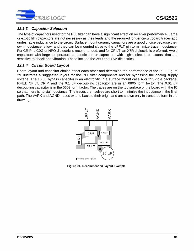
CS42526
12.1.3 Capacitor SelectionThe type of capacitors used for the PLL filter can have a significant effect on receiver performance. Largeor exotic film capacitors are not necessary as their leads and the required longer circuit board traces addundesirable inductance to the circuit. Surface mount ceramic capacitors are a good choice because theirown inductance is low, and they can be mounted close to the LPFLT pin to minimize trace inductance.For CRIP, a C0G or NPO dielectric is recommended; and for CFILT, an X7R dielectric is preferred. Avoidcapacitors with large temperature co-coefficient, or capacitors with high dielectric constants, that aresensitive to shock and vibration. These include the Z5U and Y5V dielectrics.
12.1.4 Circuit Board LayoutBoard layout and capacitor choice affect each other and determine the performance of the PLL. Figure29 illustrates a suggested layout for the PLL filter components and for bypassing the analog supplyvoltage. The 10 µF bypass capacitor is an electrolytic in a surface mount case A or thru-hole package.RFILT, CFILT, CRIP, and the 0.1 µF decoupling capacitor are in an 0805 form factor. The 0.01 µFdecoupling capacitor is in the 0603 form factor. The traces are on the top surface of the board with the ICso that there is no via inductance. The traces themselves are short to minimize the inductance in the filterpath. The VARX and AGND traces extend back to their origin and are shown only in truncated form in thedrawing.
VA
RX
AG
ND
LPF
LT
CFILT
RFI
LT
CRIP
0.1 µF
0.01 µF
10 µF= via to ground plane
Figure 29. Recommended Layout Example
DS585PP5 81
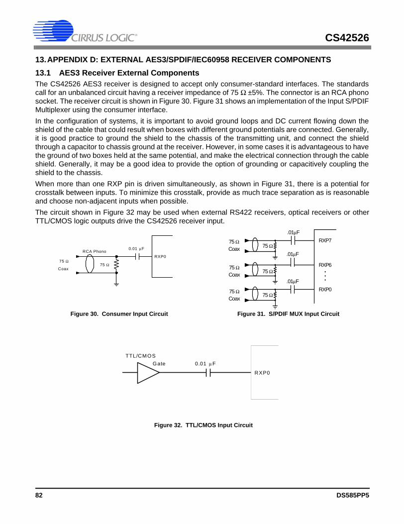
CS42526
13.APPENDIX D: EXTERNAL AES3/SPDIF/IEC60958 RECEIVER COMPONENTS 13.1 AES3 Receiver External ComponentsThe CS42526 AES3 receiver is designed to accept only consumer-standard interfaces. The standardscall for an unbalanced circuit having a receiver impedance of 75 Ω ±5%. The connector is an RCA phonosocket. The receiver circuit is shown in Figure 30. Figure 31 shows an implementation of the Input S/PDIFMultiplexer using the consumer interface.In the configuration of systems, it is important to avoid ground loops and DC current flowing down theshield of the cable that could result when boxes with different ground potentials are connected. Generally,it is good practice to ground the shield to the chassis of the transmitting unit, and connect the shieldthrough a capacitor to chassis ground at the receiver. However, in some cases it is advantageous to havethe ground of two boxes held at the same potential, and make the electrical connection through the cableshield. Generally, it may be a good idea to provide the option of grounding or capacitively coupling theshield to the chassis.When more than one RXP pin is driven simultaneously, as shown in Figure 31, there is a potential forcrosstalk between inputs. To minimize this crosstalk, provide as much trace separation as is reasonableand choose non-adjacent inputs when possible.The circuit shown in Figure 32 may be used when external RS422 receivers, optical receivers or otherTTL/CMOS logic outputs drive the CS42526 receiver input.
RXP7
RXP0
RXP6
75 Ω
.01µF
.01µF
.01µF
.
..
75 ΩCoax
75 Ω
75 Ω75 ΩCoax
75 ΩCoax
Figure 30. Consumer Input Circuit Figure 31. S/PDIF MUX Input Circuit
RCA PhonoRXP0
Coax
75 Ω75 Ω
0.01 µF
RXP0
0.01 µ FTTL/CMOS
Gate
Figure 32. TTL/CMOS Input Circuit
82 DS585PP5
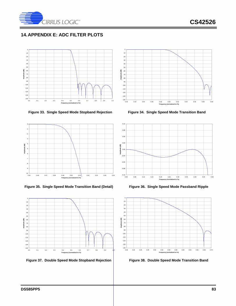
CS42526
14.APPENDIX E: ADC FILTER PLOTS
-140
-130
-120
-110
-100
-90
-80
-70
-60
-50
-40
-30
-20
-10
0
0.0 0.1 0.2 0.3 0.4 0.5 0.6 0.7 0.8 0.9 1.0
Frequency (normalized to Fs)
Am
plitu
de (d
B)
-140
-130
-120
-110
-100
-90
-80
-70
-60
-50
-40
-30
-20
-10
0
0.40 0.42 0.44 0.46 0.48 0.50 0.52 0.54 0.56 0.58 0.60
Frequency (normalized to Fs)
Am
plitu
de (d
B)
Figure 33. Single Speed Mode Stopband Rejection Figure 34. Single Speed Mode Transition Band
-10
-9
-8
-7
-6
-5
-4
-3
-2
-1
0
0.45 0.46 0.47 0.48 0.49 0.50 0.51 0.52 0.53 0.54 0.55
Frequency (normalized to Fs)
Am
plitu
de (d
B)
-0.10
-0.08
-0.05
-0.03
0.00
0.03
0.05
0.08
0.10
0.00 0.05 0.10 0.15 0.20 0.25 0.30 0.35 0.40 0.45 0.50
Frequency (normalized to Fs)
Am
plitu
de (d
B)
Figure 35. Single Speed Mode Transition Band (Detail) Figure 36. Single Speed Mode Passband Ripple
-140
-130
-120
-110
-100
-90
-80
-70
-60
-50
-40
-30
-20
-10
0
0.0 0.1 0.2 0.3 0.4 0.5 0.6 0.7 0.8 0.9 1.0
Frequency (normalized to Fs)
Am
plitu
de (d
B)
-140
-130
-120
-110
-100
-90
-80
-70
-60
-50
-40
-30
-20
-10
0
0.40 0.43 0.45 0.48 0.50 0.53 0.55 0.58 0.60 0.63 0.65 0.68 0.70
Frequency (normalized to Fs)
Am
plitu
de (d
B)
Figure 37. Double Speed Mode Stopband Rejection Figure 38. Double Speed Mode Transition Band
DS585PP5 83
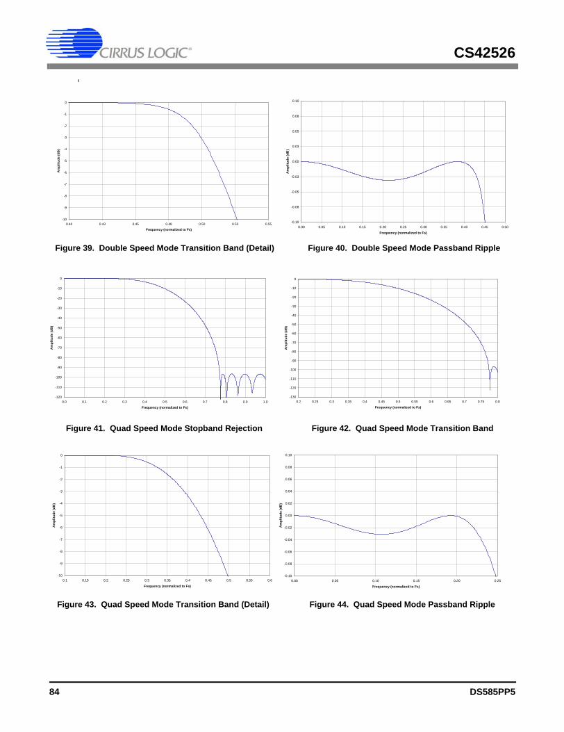
CS42526
‘
-10
-9
-8
-7
-6
-5
-4
-3
-2
-1
0
0.40 0.43 0.45 0.48 0.50 0.53 0.55
Frequency (normalized to Fs)
Am
plitu
de (d
B)
-0.10
-0.08
-0.05
-0.03
0.00
0.03
0.05
0.08
0.10
0.00 0.05 0.10 0.15 0.20 0.25 0.30 0.35 0.40 0.45 0.50
Frequency (normalized to Fs)
Am
plitu
de (d
B)
Figure 39. Double Speed Mode Transition Band (Detail) Figure 40. Double Speed Mode Passband Ripple
-120
-110
-100
-90
-80
-70
-60
-50
-40
-30
-20
-10
0
0.0 0.1 0.2 0.3 0.4 0.5 0.6 0.7 0.8 0.9 1.0
Frequency (normalized to Fs)
Am
plitu
de (d
B)
-130
-120
-110
-100
-90
-80
-70
-60
-50
-40
-30
-20
-10
0
0.2 0.25 0.3 0.35 0.4 0.45 0.5 0.55 0.6 0.65 0.7 0.75 0.8
Frequency (normalized to Fs)
Am
plitu
de (d
B)
Figure 41. Quad Speed Mode Stopband Rejection Figure 42. Quad Speed Mode Transition Band
-10
-9
-8
-7
-6
-5
-4
-3
-2
-1
0
0.1 0.15 0.2 0.25 0.3 0.35 0.4 0.45 0.5 0.55 0.6
Frequency (normalized to Fs)
Am
plitu
de (d
B)
-0.10
-0.08
-0.06
-0.04
-0.02
0.00
0.02
0.04
0.06
0.08
0.10
0.00 0.05 0.10 0.15 0.20 0.25
Frequency (normalized to Fs)
Am
plitu
de (d
B)
Figure 43. Quad Speed Mode Transition Band (Detail) Figure 44. Quad Speed Mode Passband Ripple
84 DS585PP5
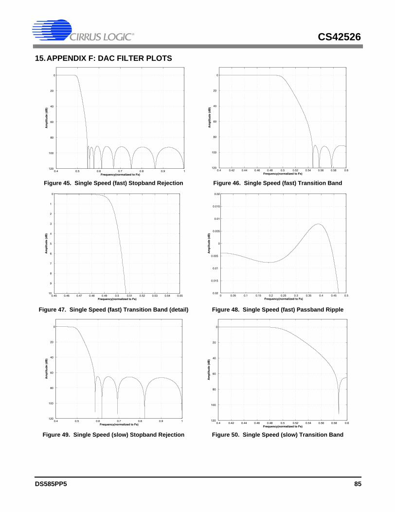
CS42526
15.APPENDIX F: DAC FILTER PLOTS
0.4 0.5 0.6 0.7 0.8 0.9 1120
100
80
60
40
20
0
Frequency(normalized to Fs)
Am
plit
ud
e (d
B)
0.4 0.42 0.44 0.46 0.48 0.5 0.52 0.54 0.56 0.58 0.6120
100
80
60
40
20
0
Frequency(normalized to Fs)
Am
plit
ud
e (d
B)
Figure 45. Single Speed (fast) Stopband Rejection Figure 46. Single Speed (fast) Transition Band
0.45 0.46 0.47 0.48 0.49 0.5 0.51 0.52 0.53 0.54 0.5510
9
8
7
6
5
4
3
2
1
0
Frequency(normalized to Fs)
Am
plit
ud
e (d
B)
0 0.05 0.1 0.15 0.2 0.25 0.3 0.35 0.4 0.45 0.50.02
0.015
0.01
0.005
0
0.005
0.01
0.015
0.02
Frequency(normalized to Fs)
Am
plit
ud
e (d
B)
Figure 47. Single Speed (fast) Transition Band (detail) Figure 48. Single Speed (fast) Passband Ripple
0.4 0.5 0.6 0.7 0.8 0.9 1120
100
80
60
40
20
0
Frequency(normalized to Fs)
Am
plit
ud
e (d
B)
0.4 0.42 0.44 0.46 0.48 0.5 0.52 0.54 0.56 0.58 0.6120
100
80
60
40
20
0
Frequency(normalized to Fs)
Am
plit
ud
e (d
B)
Figure 49. Single Speed (slow) Stopband Rejection Figure 50. Single Speed (slow) Transition Band
DS585PP5 85
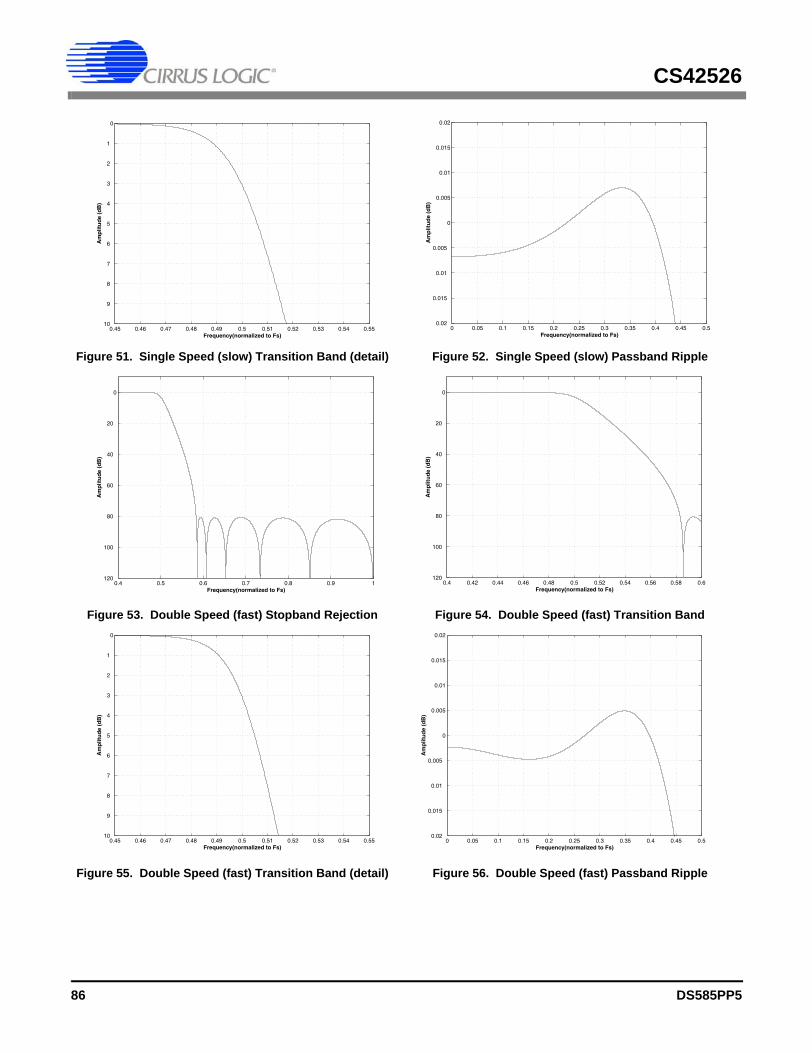
CS42526
0 0.05 0.1 0.15 0.2 0.25 0.3 0.35 0.4 0.45 0.50.02
0.015
0.01
0.005
0
0.005
0.01
0.015
0.02
Frequency(normalized to Fs)
Am
plit
ud
e (d
B)
0.45 0.46 0.47 0.48 0.49 0.5 0.51 0.52 0.53 0.54 0.5510
9
8
7
6
5
4
3
2
1
0
Frequency(normalized to Fs)
Am
plit
ud
e (d
B)
Figure 51. Single Speed (slow) Transition Band (detail) Figure 52. Single Speed (slow) Passband Ripple
0.4 0.5 0.6 0.7 0.8 0.9 1120
100
80
60
40
20
0
Frequency(normalized to Fs)
Am
plit
ud
e (d
B)
0.4 0.42 0.44 0.46 0.48 0.5 0.52 0.54 0.56 0.58 0.6120
100
80
60
40
20
0
Frequency(normalized to Fs)
Am
plit
ud
e (d
B)
Figure 53. Double Speed (fast) Stopband Rejection Figure 54. Double Speed (fast) Transition Band
0.45 0.46 0.47 0.48 0.49 0.5 0.51 0.52 0.53 0.54 0.5510
9
8
7
6
5
4
3
2
1
0
Frequency(normalized to Fs)
Am
plit
ud
e (d
B)
0 0.05 0.1 0.15 0.2 0.25 0.3 0.35 0.4 0.45 0.50.02
0.015
0.01
0.005
0
0.005
0.01
0.015
0.02
Frequency(normalized to Fs)
Am
plit
ud
e (d
B)
Figure 55. Double Speed (fast) Transition Band (detail) Figure 56. Double Speed (fast) Passband Ripple
86 DS585PP5
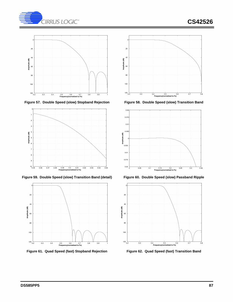
CS42526
0.2 0.3 0.4 0.5 0.6 0.7 0.8 0.9 1120
100
80
60
40
20
0
Frequency(normalized to Fs)
Am
plit
ud
e (d
B)
0.2 0.3 0.4 0.5 0.6 0.7 0.8120
100
80
60
40
20
0
Frequency(normalized to Fs)
Am
plit
ud
e (d
B)
Figure 57. Double Speed (slow) Stopband Rejection Figure 58. Double Speed (slow) Transition Band
0.45 0.46 0.47 0.48 0.49 0.5 0.51 0.52 0.53 0.54 0.5510
9
8
7
6
5
4
3
2
1
0
Frequency(normalized to Fs)
Am
plit
ud
e (d
B)
0 0.05 0.1 0.15 0.2 0.25 0.3 0.350.02
0.015
0.01
0.005
0
0.005
0.01
0.015
0.02
Frequency(normalized to Fs)
Am
plit
ud
e (d
B)
Figure 59. Double Speed (slow) Transition Band (detail) Figure 60. Double Speed (slow) Passband Ripple
0.2 0.3 0.4 0.5 0.6 0.7 0.8 0.9 1120
100
80
60
40
20
0
Frequency(normalized to Fs)
Am
plit
ud
e (d
B)
0.2 0.3 0.4 0.5 0.6 0.7 0.8120
100
80
60
40
20
0
Frequency(normalized to Fs)
Am
plit
ud
e (d
B)
Figure 61. Quad Speed (fast) Stopband Rejection Figure 62. Quad Speed (fast) Transition Band
DS585PP5 87
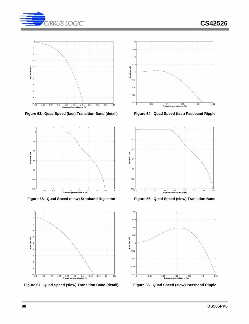
CS42526
0.45 0.46 0.47 0.48 0.49 0.5 0.51 0.52 0.53 0.54 0.5510
9
8
7
6
5
4
3
2
1
0
Frequency(normalized to Fs)
Am
plit
ud
e (d
B)
0 0.05 0.1 0.15 0.2 0.250.2
0.15
0.1
0.05
0
0.05
0.1
0.15
0.2
Frequency(normalized to Fs)
Am
plit
ud
e (d
B)
Figure 63. Quad Speed (fast) Transition Band (detail) Figure 64. Quad Speed (fast) Passband Ripple
0.1 0.2 0.3 0.4 0.5 0.6 0.7 0.8 0.9 1120
100
80
60
40
20
0
Frequency(normalized to Fs)
Am
plit
ud
e (d
B)
0.1 0.2 0.3 0.4 0.5 0.6 0.7 0.8 0.9120
100
80
60
40
20
0
Frequency(normalized to Fs)
Am
plit
ud
e (d
B)
Figure 65. Quad Speed (slow) Stopband Rejection Figure 66. Quad Speed (slow) Transition Band
0.45 0.46 0.47 0.48 0.49 0.5 0.51 0.52 0.53 0.54 0.5510
9
8
7
6
5
4
3
2
1
0
Frequency(normalized to Fs)
Am
plit
ud
e (d
B)
0 0.02 0.04 0.06 0.08 0.1 0.120.02
0.015
0.01
0.005
0
0.005
0.01
0.015
0.02
Frequency(normalized to Fs)
Am
plit
ud
e (d
B)
Figure 67. Quad Speed (slow) Transition Band (detail) Figure 68. Quad Speed (slow) Passband Ripple
88 DS585PP5
CS42526
Table 22. Revision History Release Date Changes
A1 December 2002 Advance ReleasePP1 August 2003 Preliminary ReleasePP2 August 2003 – Added Revision History table.
– Updated registers 6.7.4 and 6.7.5 on page 53.PP3 March 2004 Corrected error in document title.PP4 July 2004 Add lead free part numbersPP5 January 2005 – Updated PLL components in Table 21 on page 80.
– Added PDN_RCVR1 bit and description on page 47.– Added LOCKM bit and description on page 65.– Added OMCK Frequency specification in the Switching Characteristics table on
page 12.– Updated ADC Input Impedance and Offset Error specifications in the Analog
Input Characteristics table on page 8.– Updated the DAC Full Scale Voltage, Output Impedance, and Gain Drift
specifications in the Analog Output Characteristics table on page 10.– Updated specification conditions for the analog input characteristics on page 8.– Updated specification conditions for the analog output characteristics on
page 10.– Updated specification of tds and tdh in the Switching Characteristics table on
page 12.– Corrected reference to the SW_CTRL[1:0] bits in section 4.5.3 on page 26.– Moved the VQ and FILT+ specifications from the Analog Input Characteristics
table on page 8 to the DC Electrical Characteristics table on page 15.– Updated the Power Supply Current and Power Consumption specifications in
the DC Electrical Characteristics table on page 15.– Updated the description of the CONF bit on page page 67.– Updated Table 13 on page 54 to include HDCD format detection.– Corrected default value of the Chip_ID[3:0] bits in register 01h on pages 42 and
46.– Updated default value of the Rev_ID[3:0] bits in register 01h on pages 42 and
46.
DS585PP5 89
CS42526
IMPORTANT NOTICE"Preliminary" product information describes products that are in production, but for which full characterization data is not yet available. Cirrus Logic, Inc. and its subsidiaries ("Cirrus") believe that the information contained in this document is accurate and reliable. However, the infor-mation is subject to change without notice and is provided "AS IS" without warranty of any kind (express or implied). Customers are advised to obtainthe latest version of relevant information to verify, before placing orders, that information being relied on is current and complete. All products aresold subject to the terms and conditions of sale supplied at the time of order acknowledgment, including those pertaining to warranty, indemnification,and limitation of liability. No responsibility is assumed by Cirrus for the use of this information, including use of this information as the basis for man-ufacture or sale of any items, or for infringement of patents or other rights of third parties. This document is the property of Cirrus and by furnishingthis information, Cirrus grants no license, express or implied under any patents, mask work rights, copyrights, trademarks, trade secrets or otherintellectual property rights. Cirrus owns the copyrights associated with the information contained herein and gives consent for copies to be made ofthe information only for use within your organization with respect to Cirrus integrated circuits or other products of Cirrus. This consent does not extendto other copying such as copying for general distribution, advertising or promotional purposes, or for creating any work for resale.
CERTAIN APPLICATIONS USING SEMICONDUCTOR PRODUCTS MAY INVOLVE POTENTIAL RISKS OF DEATH, PERSONAL INJURY, ORSEVERE PROPERTY OR ENVIRONMENTAL DAMAGE ("CRITICAL APPLICATIONS"). CIRRUS PRODUCTS ARE NOT DESIGNED, AUTHO-RIZED OR WARRANTED FOR USE IN AIRCRAFT SYSTEMS, MILITARY APPLICATIONS, PRODUCTS SURGICALLY IMPLANTED INTO THEBODY, AUTOMOTIVE SAFETY OR SECURITY DEVICES, LIFE SUPPORT PRODUCTS OR OTHER CRITICAL APPLICATIONS. INCLUSION OFCIRRUS PRODUCTS IN SUCH APPLICATIONS IS UNDERSTOOD TO BE FULLY AT THE CUSTOMER'S RISK AND CIRRUS DISCLAIMS ANDMAKES NO WARRANTY, EXPRESS, STATUTORY OR IMPLIED, INCLUDING THE IMPLIED WARRANTIES OF MERCHANTABILITY AND FIT-NESS FOR PARTICULAR PURPOSE, WITH REGARD TO ANY CIRRUS PRODUCT THAT IS USED IN SUCH A MANNER. IF THE CUSTOMEROR CUSTOMER'S CUSTOMER USES OR PERMITS THE USE OF CIRRUS PRODUCTS IN CRITICAL APPLICATIONS, CUSTOMER AGREES,BY SUCH USE, TO FULLY INDEMNIFY CIRRUS, ITS OFFICERS, DIRECTORS, EMPLOYEES, DISTRIBUTORS AND OTHER AGENTS FROMANY AND ALL LIABILITY, INCLUDING ATTORNEYS' FEES AND COSTS, THAT MAY RESULT FROM OR ARISE IN CONNECTION WITH THESEUSES.
Cirrus Logic, Cirrus, and the Cirrus Logic logo designs are trademarks of Cirrus Logic, Inc. All other brand and product names in this document maybe trademarks or service marks of their respective owners.AC-3 is a registered trademark of Dolby Laboratories, Inc.DTS is a registered trademark of the Digital Theater Systems, Inc. SPI is a trademark of Motorola, Inc.
Contacting Cirrus Logic SupportFor all product questions and inquiries contact a Cirrus Logic Sales Representative. To find one nearest you go to http://www.cirrus.com/
90 DS585PP5