Embed Size (px)
Citation preview
1
CS 61C: Great Ideas in Computer Architecture
Finite State Machines
Instructors:Krste Asanovic & Vladimir Stojanovic
http://inst.eecs.berkeley.edu/~cs61c/sp15
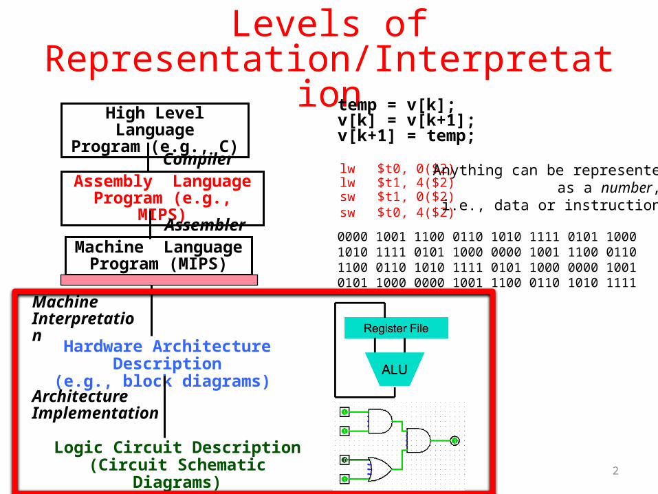
Levels of Representation/Interpretation
lw $t0, 0($2)lw $t1, 4($2)sw $t1, 0($2)sw $t0, 4($2)
High Level LanguageProgram (e.g., C)
Assembly Language Program (e.g., MIPS)
Machine Language Program (MIPS)
Hardware Architecture Description(e.g., block diagrams)
Compiler
Assembler
Machine Interpretation
temp = v[k];v[k] = v[k+1];v[k+1] = temp;
0000 1001 1100 0110 1010 1111 0101 10001010 1111 0101 1000 0000 1001 1100 0110 1100 0110 1010 1111 0101 1000 0000 1001 0101 1000 0000 1001 1100 0110 1010 1111
Logic Circuit Description(Circuit Schematic Diagrams)
Architecture Implementation
Anything can be representedas a number,
i.e., data or instructions
2
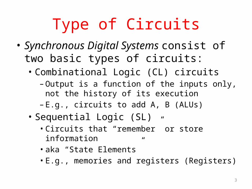
Type of Circuits• Synchronous Digital Systems consist of two
basic types of circuits:• Combinational Logic (CL) circuits
– Output is a function of the inputs only, not the history of its execution
– E.g., circuits to add A, B (ALUs)
• Sequential Logic (SL)• Circuits that “remember” or store information• aka “State Elements”• E.g., memories and registers (Registers)
3
Uses for State Elements
• Place to store values for later re-use:– Register files (like $1-$31 in MIPS)– Memory (caches and main memory)
• Help control flow of information between combinational logic blocks– State elements hold up the movement of
information at input to combinational logic blocks to allow for orderly passage
4
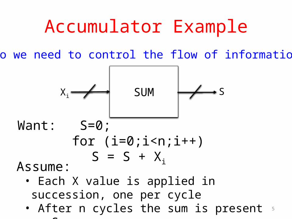
Accumulator Example
Want: S=0; for (i=0;i<n;i++)
S = S + Xi
Why do we need to control the flow of information?
Assume:• Each X value is applied in succession, one per cycle• After n cycles the sum is present on S
5
SUMXi S
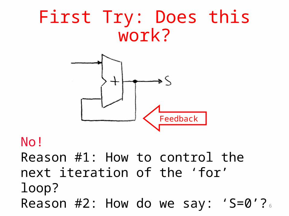
First Try: Does this work?
6
No! Reason #1: How to control the next iteration of the ‘for’ loop?Reason #2: How do we say: ‘S=0’?
Feedback
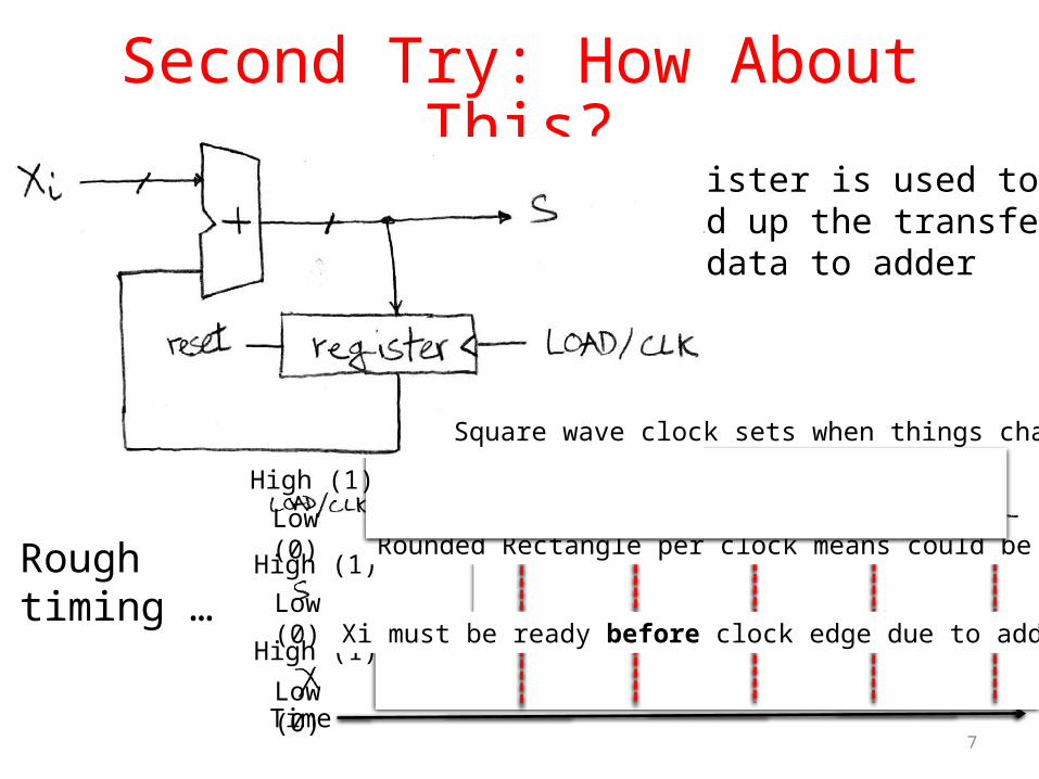
Second Try: How About This?
7
Roughtiming …
Register is used to hold up the transfer of data to adder
Time
High (1)Low (0)
High (1)
Low (0)
Rounded Rectangle per clock means could be 1 or 0
Xi must be ready before clock edge due to adder delay
High (1)Low (0)
Square wave clock sets when things change
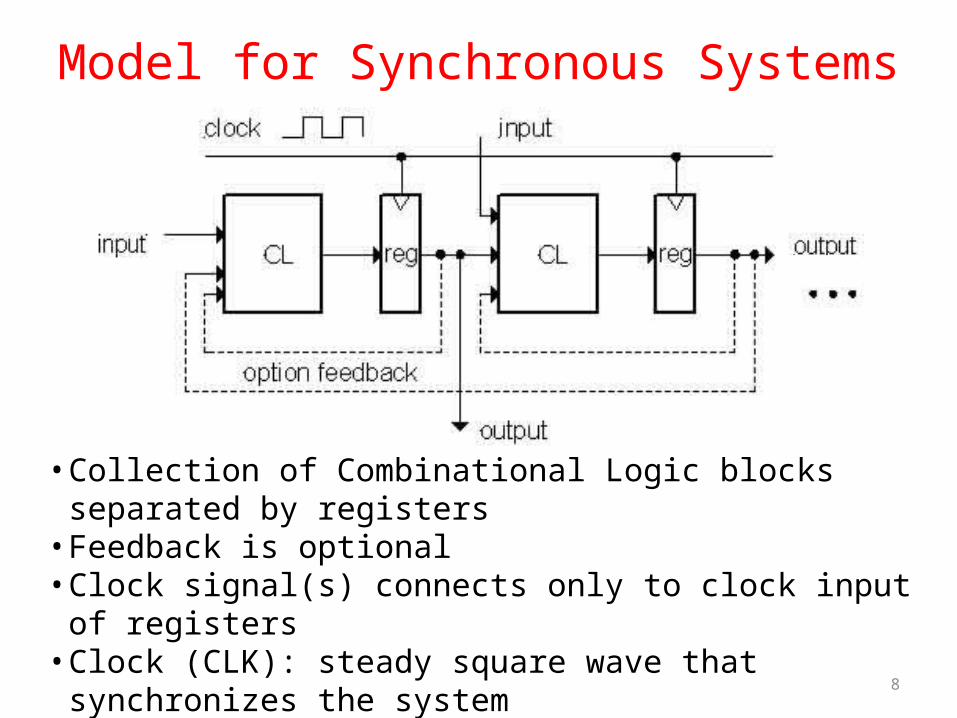
Model for Synchronous Systems
8
• Collection of Combinational Logic blocks separated by registers• Feedback is optional• Clock signal(s) connects only to clock input of registers• Clock (CLK): steady square wave that synchronizes the system• Register: several bits of state that samples on rising edge of CLK
(positive edge-triggered) or falling edge (negative edge-triggered)
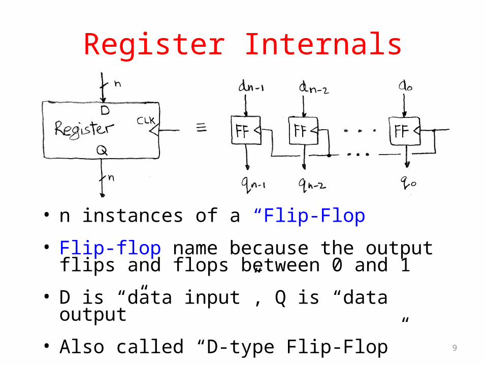
Register Internals
• n instances of a “Flip-Flop”
• Flip-flop name because the output flips and flops between 0 and 1
• D is “data input”, Q is “data output”
• Also called “D-type Flip-Flop”9
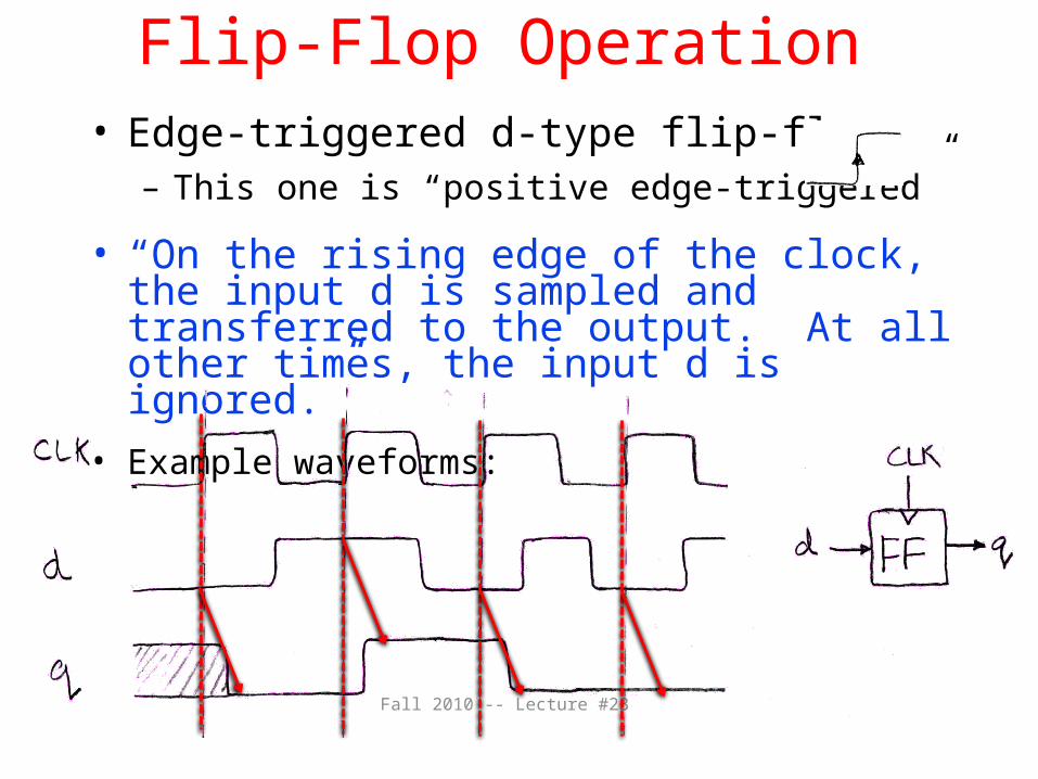
Flip-Flop Operation• Edge-triggered d-type flip-flop
– This one is “positive edge-triggered”
• “On the rising edge of the clock, the input d is sampled and transferred to the output. At all other times, the input d is ignored.”
• Example waveforms:
Fall 2010 -- Lecture #23
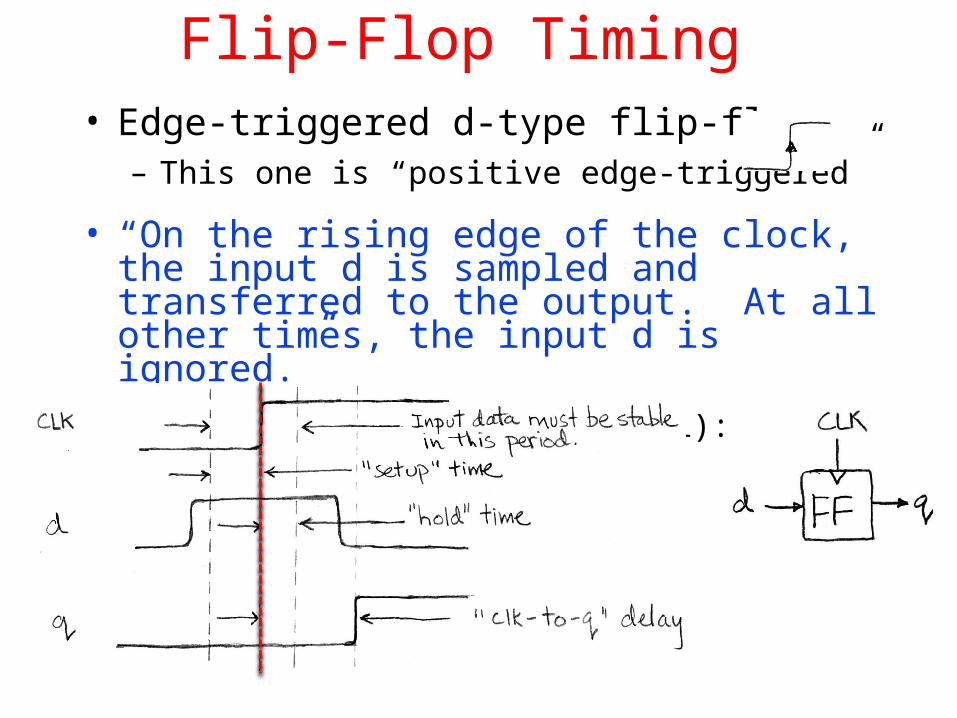
Flip-Flop Timing• Edge-triggered d-type flip-flop
– This one is “positive edge-triggered”
• “On the rising edge of the clock, the input d is sampled and transferred to the output. At all other times, the input d is ignored.”
• Example waveforms (more detail):
12
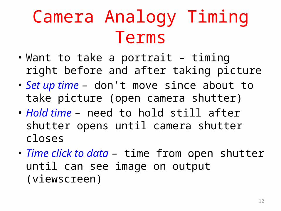
Camera Analogy Timing Terms
• Want to take a portrait – timing right before and after taking picture
• Set up time – don’t move since about to take picture (open camera shutter)
• Hold time – need to hold still after shutter opens until camera shutter closes
• Time click to data – time from open shutter until can see image on output (viewscreen)
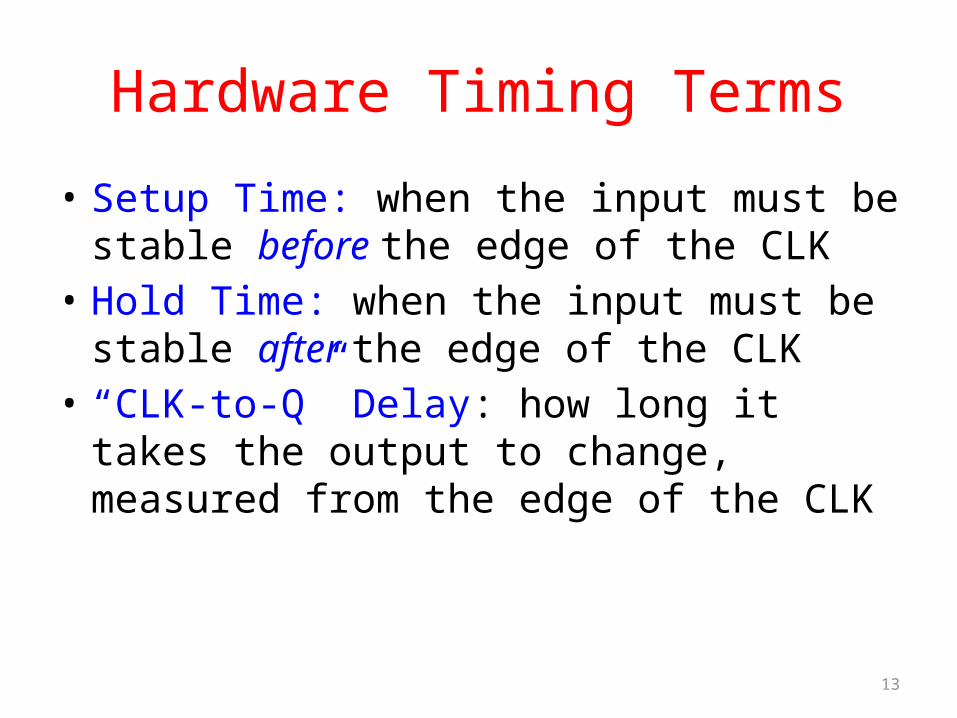
Hardware Timing Terms
• Setup Time: when the input must be stable before the edge of the CLK
• Hold Time: when the input must be stable after the edge of the CLK
• “CLK-to-Q” Delay: how long it takes the output to change, measured from the edge of the CLK
13
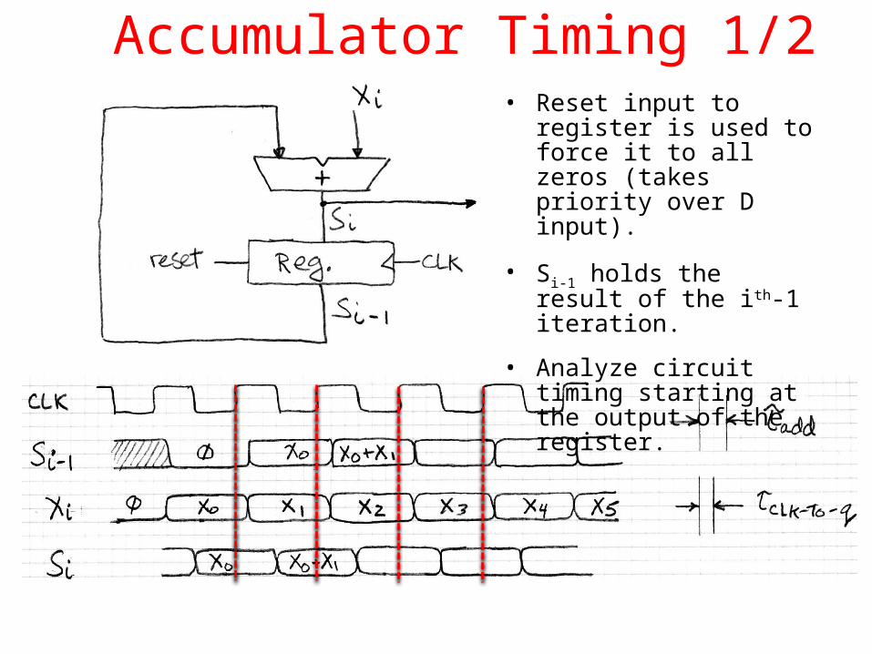
Accumulator Timing 1/2• Reset input to register is
used to force it to all zeros (takes priority over D input).
• Si-1 holds the result of the ith-1 iteration.
• Analyze circuit timing starting at the output of the register.
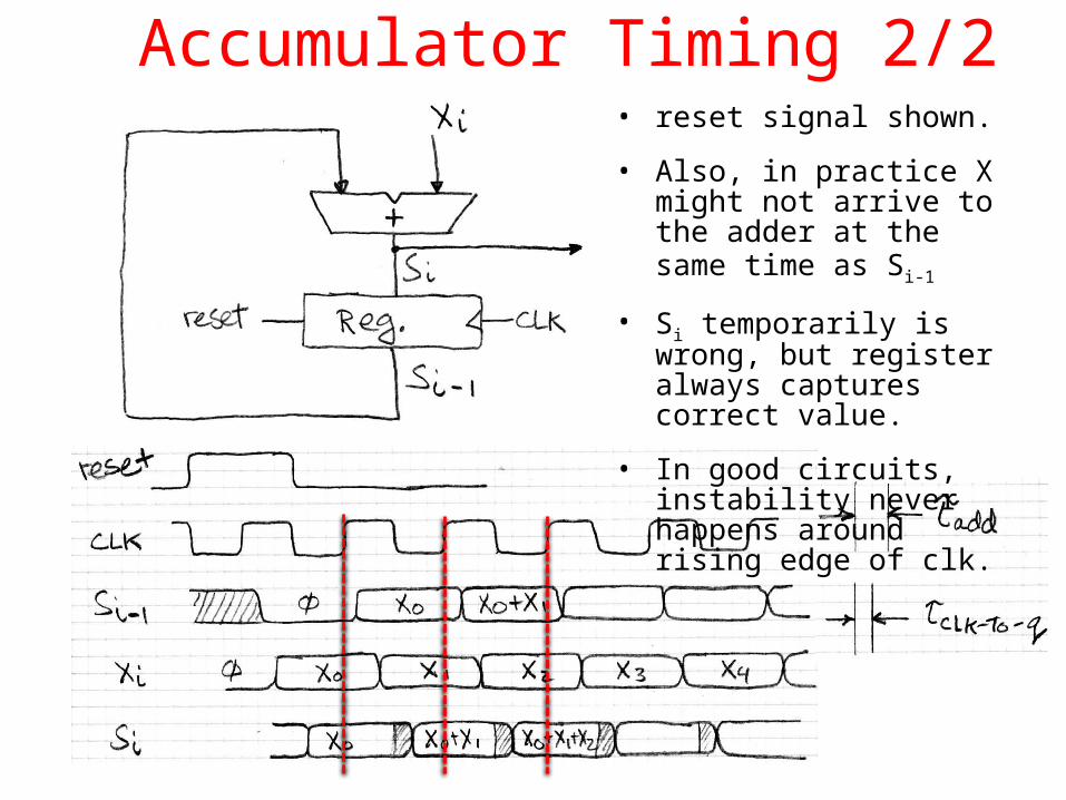
Accumulator Timing 2/2• reset signal shown.
• Also, in practice X might not arrive to the adder at the same time as Si-1
• Si temporarily is wrong, but register always captures correct value.
• In good circuits, instability never happens around rising edge of clk.
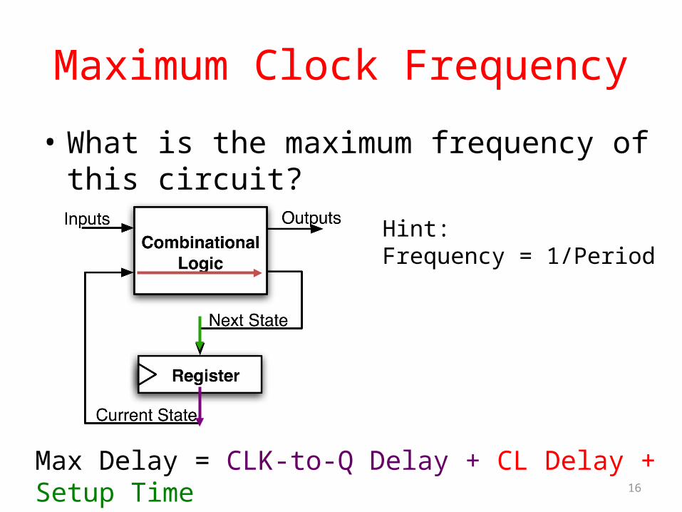
Maximum Clock Frequency
• What is the maximum frequency of this circuit?
16
Max Delay = CLK-to-Q Delay + CL Delay + Setup Time
Hint:Frequency = 1/Period
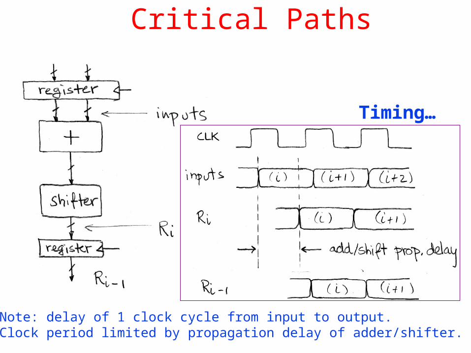
Critical Paths
Timing…
Note: delay of 1 clock cycle from input to output.Clock period limited by propagation delay of adder/shifter.
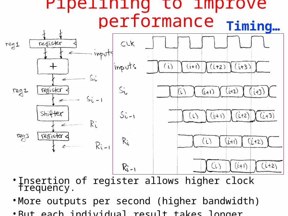
Pipelining to improve performanceTiming…
• Insertion of register allows higher clock frequency.• More outputs per second (higher bandwidth)• But each individual result takes longer (greater latency)
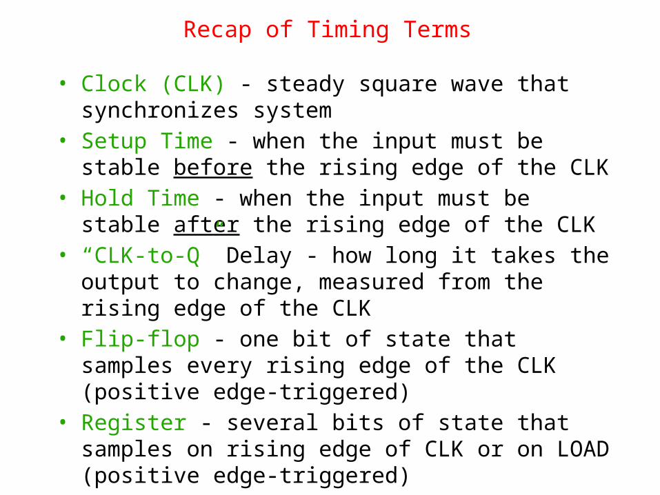
Recap of Timing Terms
• Clock (CLK) - steady square wave that synchronizes system• Setup Time - when the input must be stable before the
rising edge of the CLK• Hold Time - when the input must be stable after the rising
edge of the CLK• “CLK-to-Q” Delay - how long it takes the output to change,
measured from the rising edge of the CLK• Flip-flop - one bit of state that samples every rising edge of
the CLK (positive edge-triggered)• Register - several bits of state that samples on rising edge
of CLK or on LOAD (positive edge-triggered)
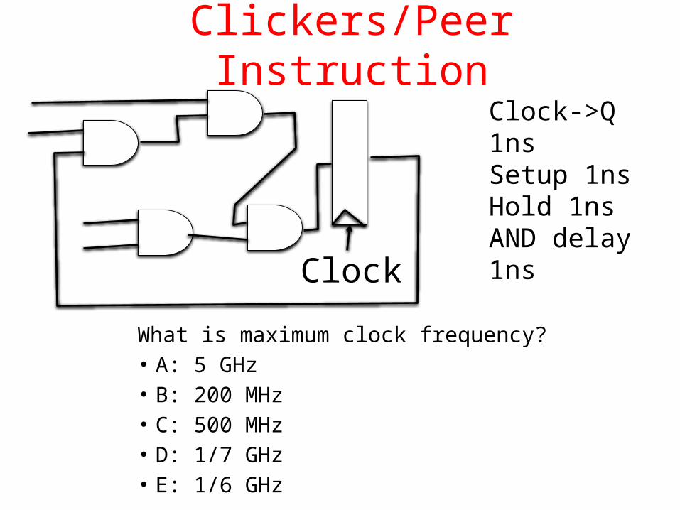
Clickers/Peer Instruction
What is maximum clock frequency?• A: 5 GHz • B: 200 MHz• C: 500 MHz• D: 1/7 GHz• E: 1/6 GHz
Clock
Clock->Q 1nsSetup 1nsHold 1nsAND delay 1ns
21
Administrivia
• Project 1-1 due 3/01• Midterm is next Thursday 2/26, in class
– Covers up to and including the previous lecture– 1 handwritten, double sided, 8.5”x11” cheat sheet– We’ll give you MIPS green sheet
• Review Sessions:– TA: Monday 2/23, 7-9pm, 10 Evans– HKN: Saturday 2/21, 1-4pm, 100 Genetics Plant
Biology
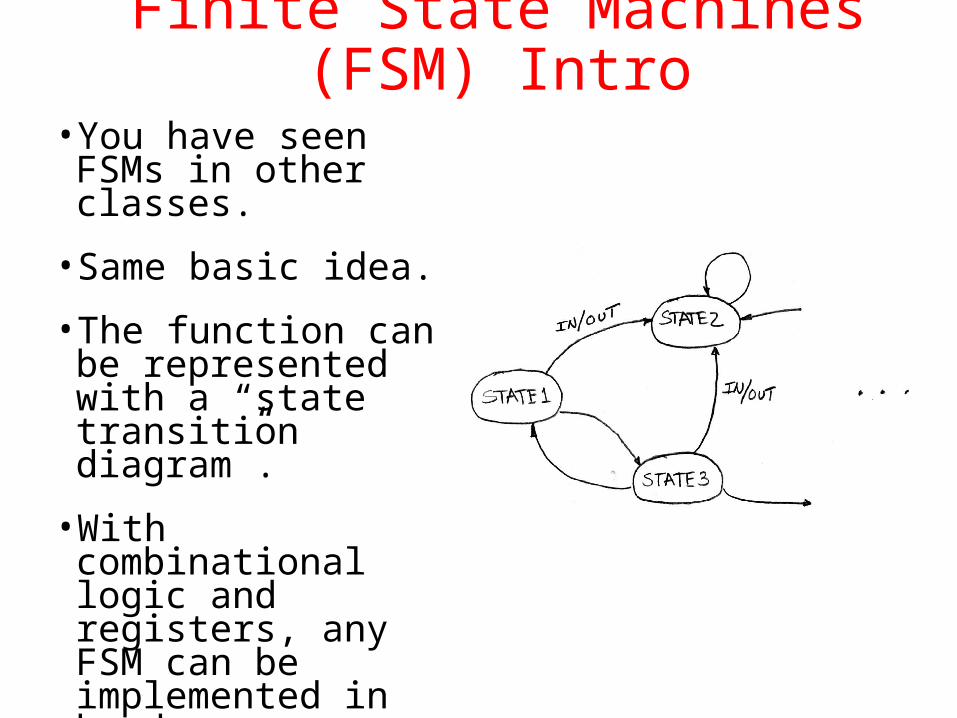
Finite State Machines (FSM) Intro• You have seen FSMs
in other classes.
• Same basic idea.
• The function can be represented with a “state transition diagram”.
•With combinational logic and registers, any FSM can be implemented in hardware.
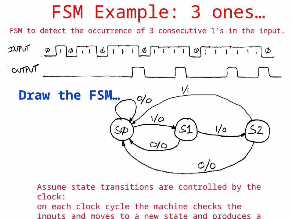
FSM Example: 3 ones…
Draw the FSM…
FSM to detect the occurrence of 3 consecutive 1’s in the input.
Assume state transitions are controlled by the clock:on each clock cycle the machine checks the inputs and moves to a new state and produces a new output…
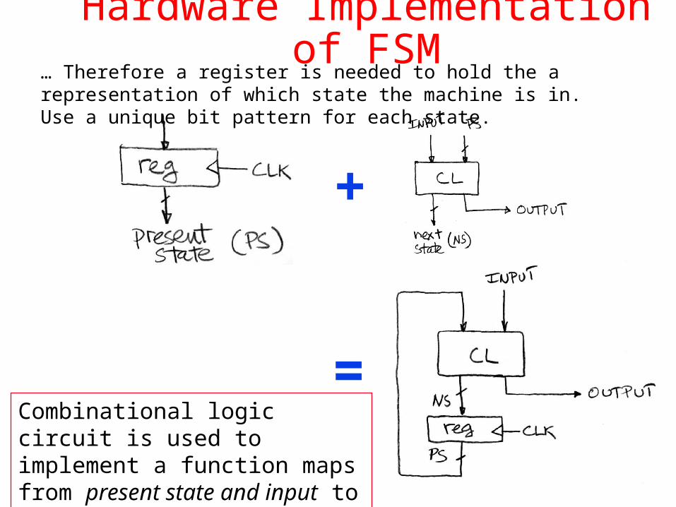
Hardware Implementation of FSM
+
= ?
… Therefore a register is needed to hold the a representation of which state the machine is in. Use a unique bit pattern for each state.
Combinational logic circuit is used to implement a function maps from present state and input to next state and output.
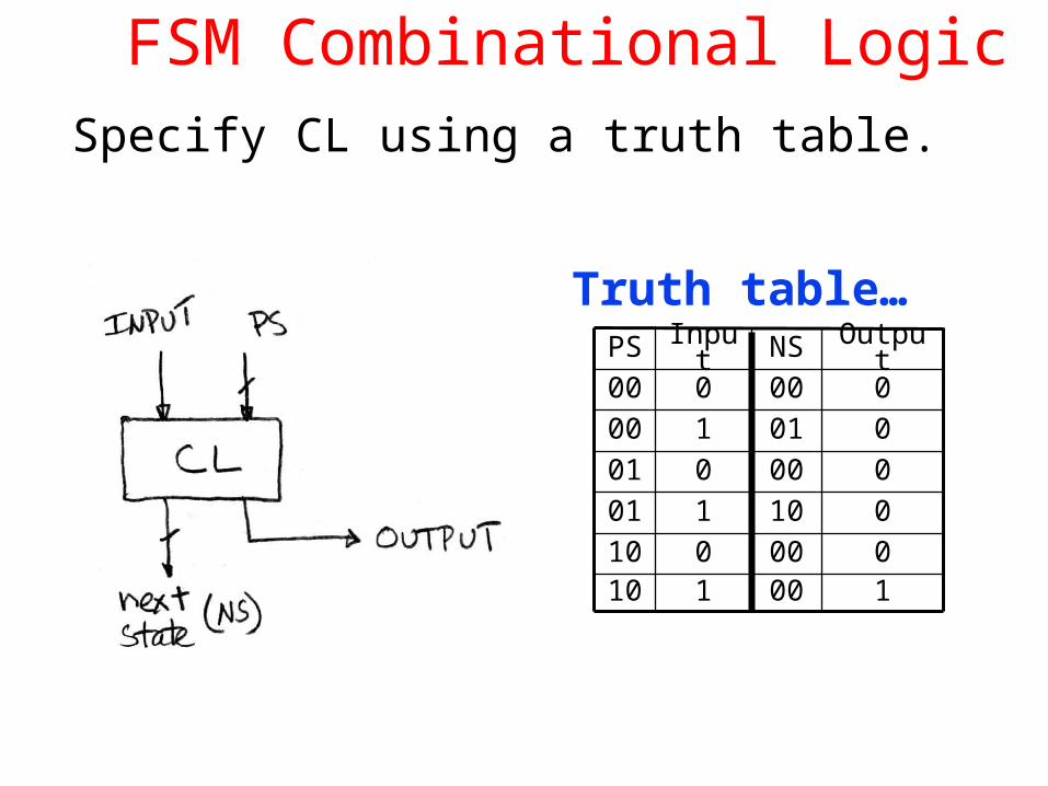
FSM Combinational Logic
100110000010
010101
000001
001100
000000
OutputNSInputPS
Truth table…
Specify CL using a truth table.
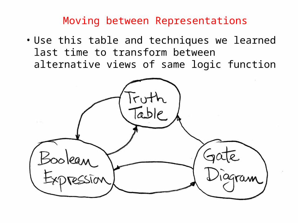
Moving between Representations
• Use this table and techniques we learned last time to transform between alternative views of same logic function
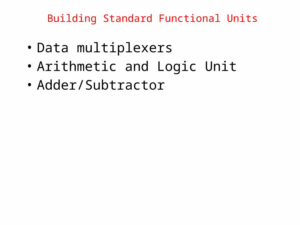
Building Standard Functional Units
• Data multiplexers• Arithmetic and Logic Unit• Adder/Subtractor
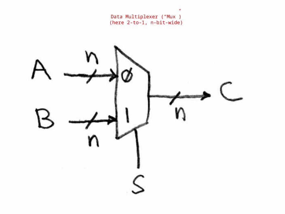
Data Multiplexer (“Mux”)(here 2-to-1, n-bit-wide)
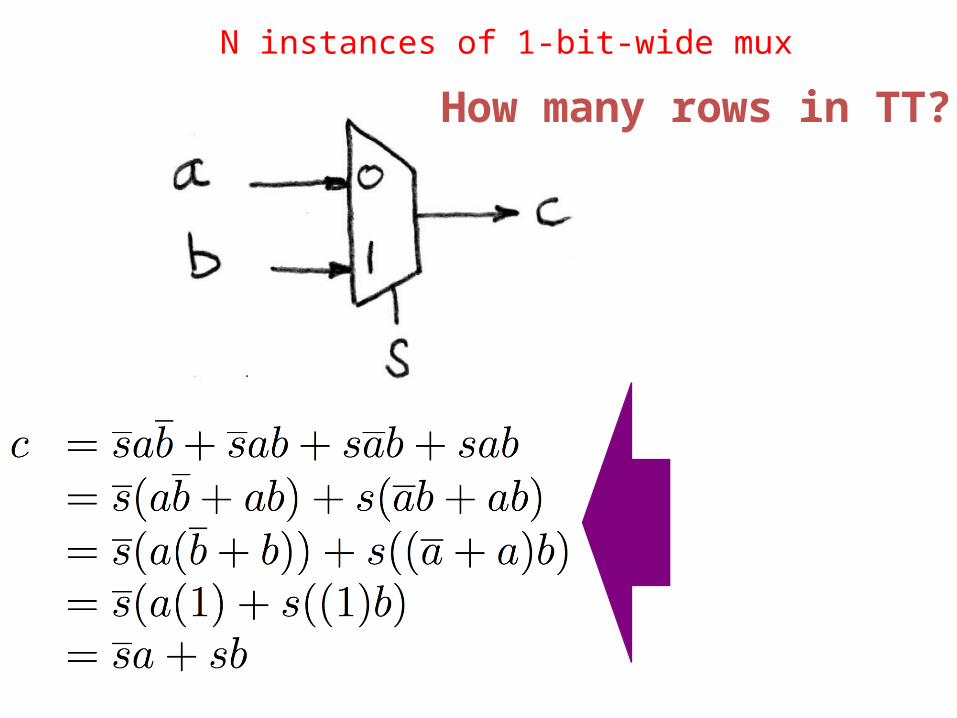
N instances of 1-bit-wide mux
How many rows in TT?
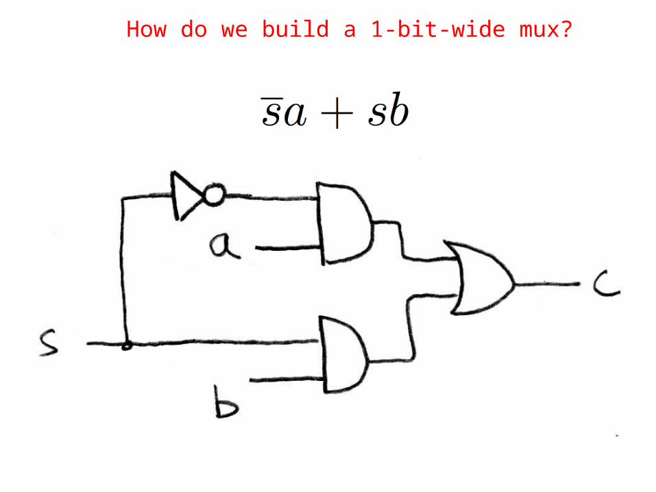
How do we build a 1-bit-wide mux?
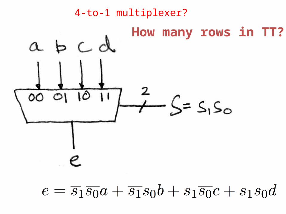
4-to-1 multiplexer?
How many rows in TT?
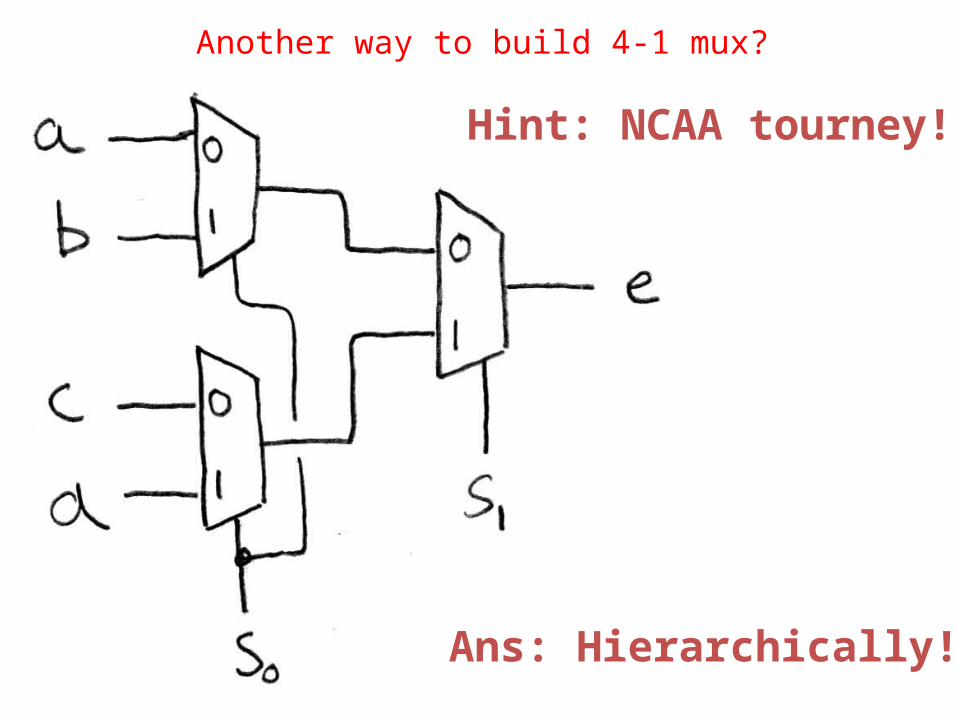
Another way to build 4-1 mux?
Hint: NCAA tourney!
Ans: Hierarchically!
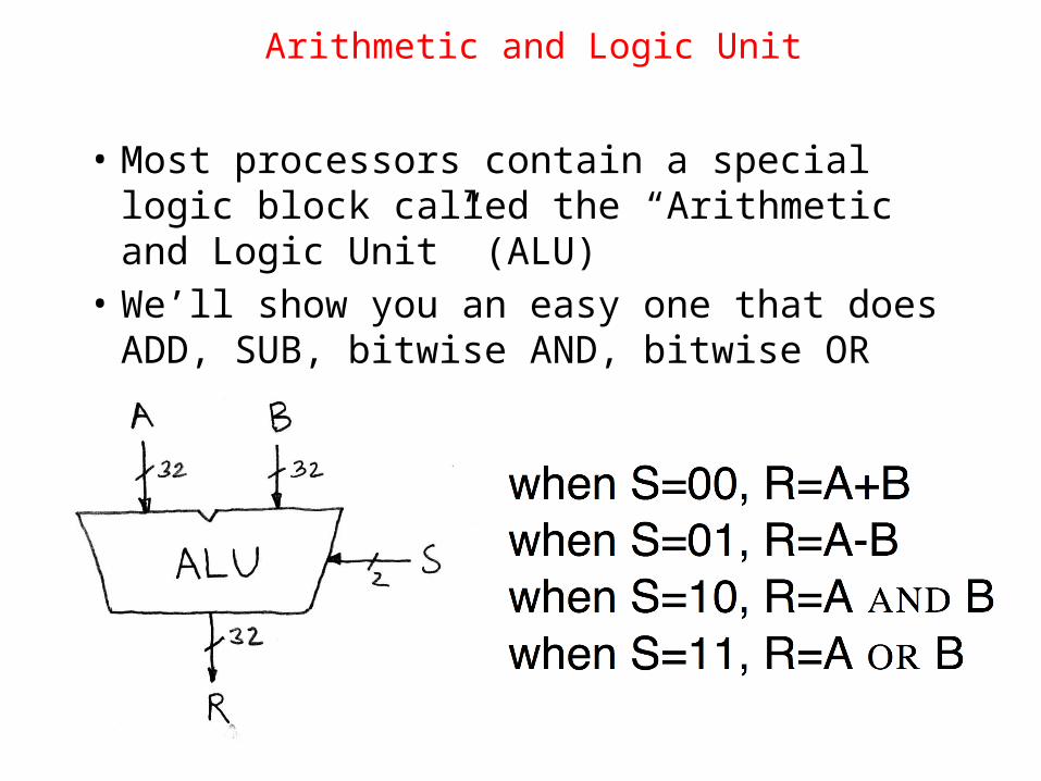
Arithmetic and Logic Unit
• Most processors contain a special logic block called the “Arithmetic and Logic Unit” (ALU)
• We’ll show you an easy one that does ADD, SUB, bitwise AND, bitwise OR
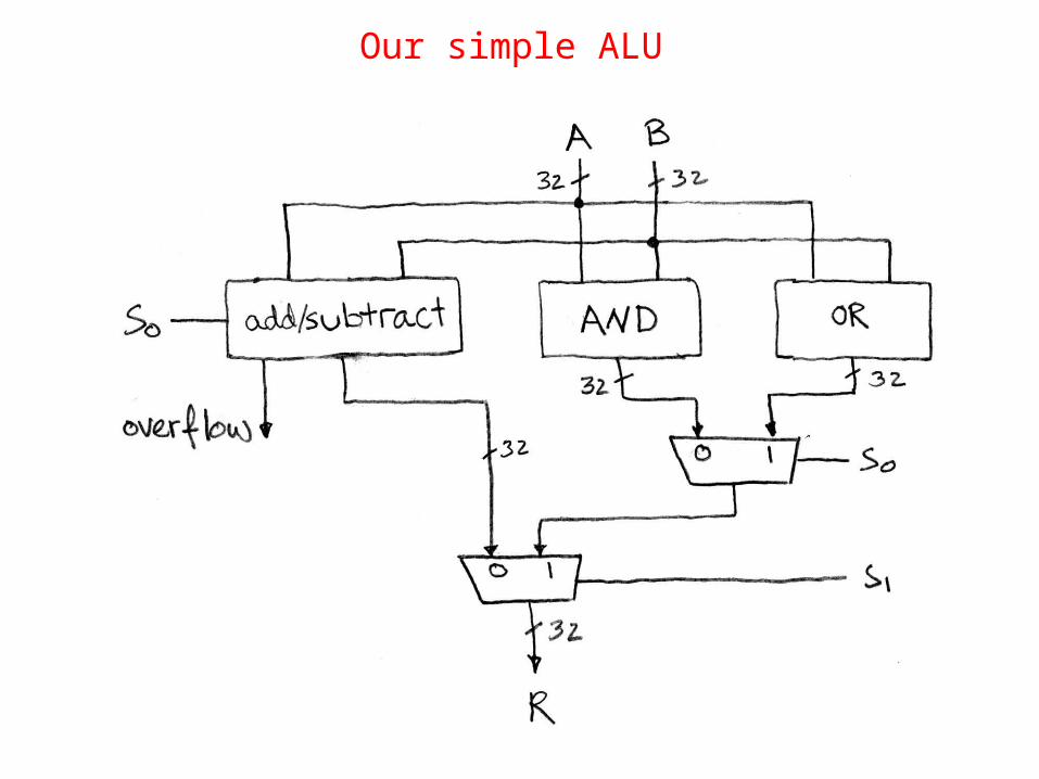
Our simple ALU

35
In the News:Microsoft, Google beat
Humans at Image Recognition (EE Times)
• On ImageNet benchmark image database, systems from Microsoft and Google performed better than humans at recognizing images
• Both companies used deep artificial neural networks to train on image database
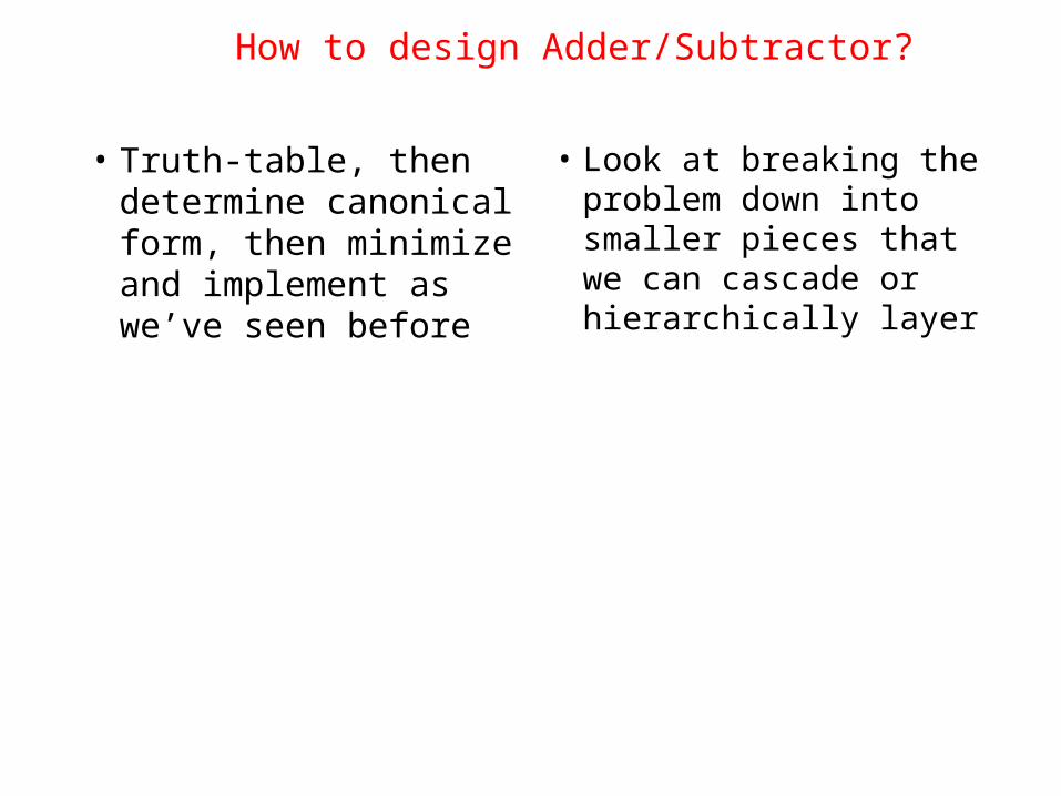
How to design Adder/Subtractor?
• Truth-table, then determine canonical form, then minimize and implement as we’ve seen before
• Look at breaking the problem down into smaller pieces that we can cascade or hierarchically layer
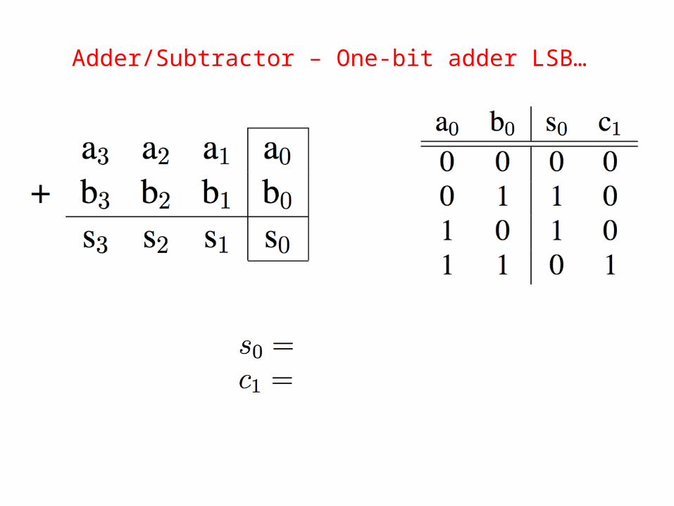
Adder/Subtractor – One-bit adder LSB…
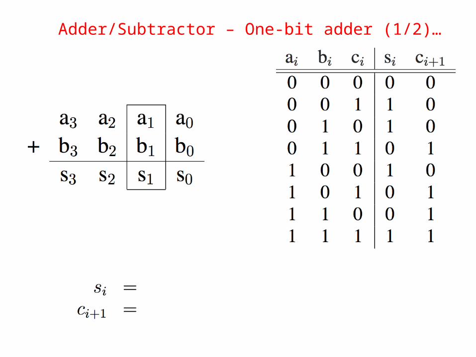
Adder/Subtractor – One-bit adder (1/2)…
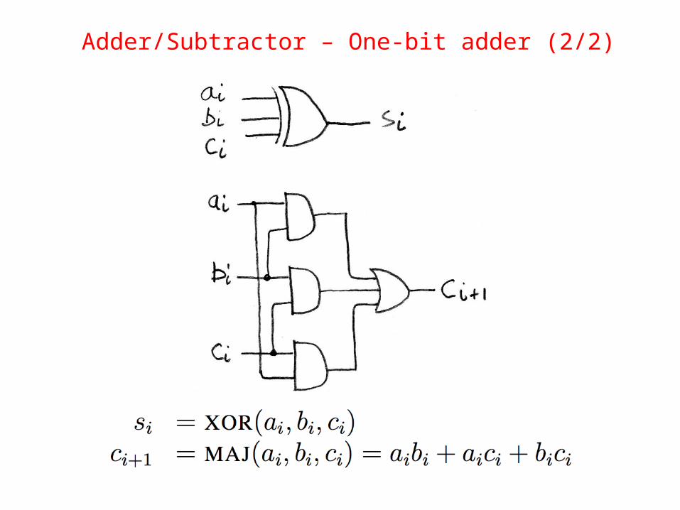
Adder/Subtractor – One-bit adder (2/2)
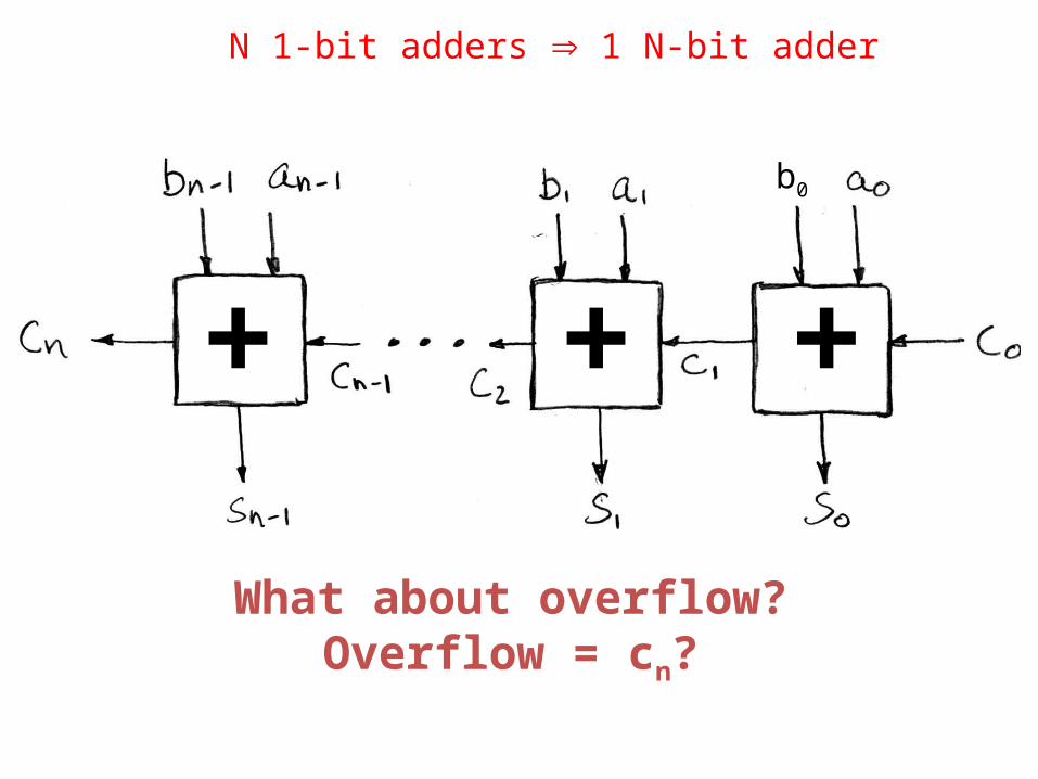
N 1-bit adders 1 N-bit adder
What about overflow?Overflow = cn?
+ + +
b0
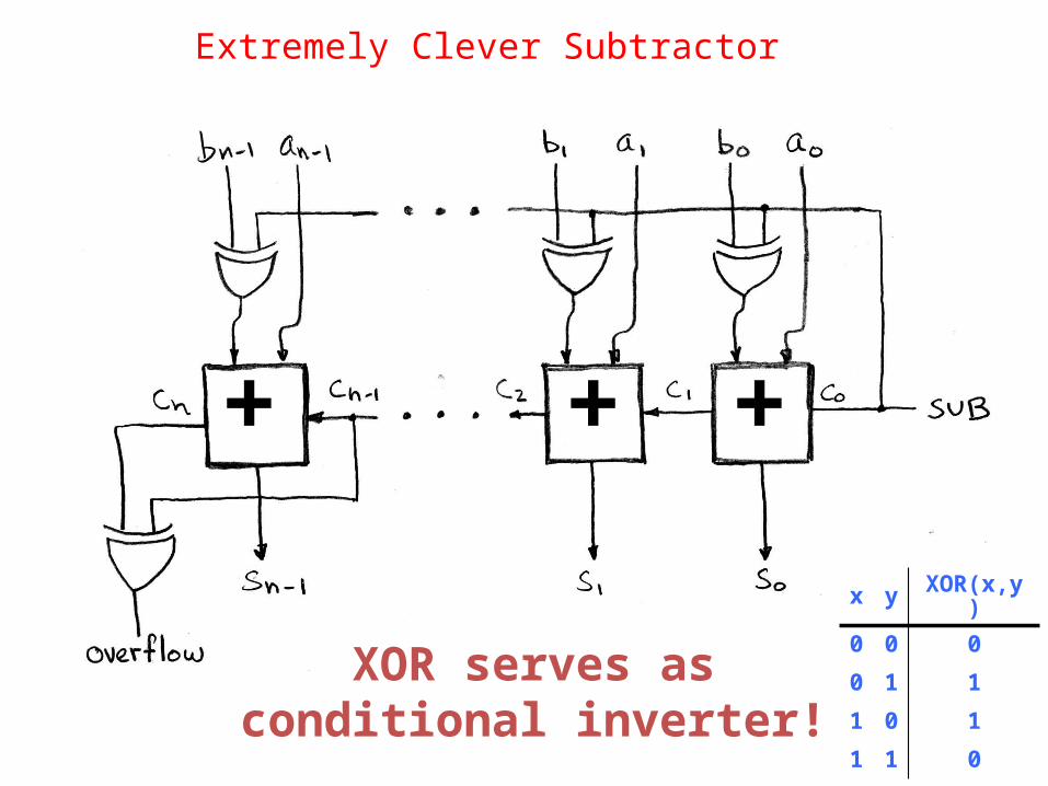
Extremely Clever Subtractor
x y XOR(x,y)
0 0 0
0 1 1
1 0 1
1 1 0
+ + +
XOR serves asconditional inverter!
42
In Conclusion
• Finite State Machines have clocked state elements plus combinational logic to describe transition between states
• Standard combinational functional unit blocks built hierarchically from subcomponents