Embed Size (px)
Citation preview
Controlling Morphology and Molecular
Order of Solution-Processed
Organic Semiconductors for Transistors
Xiaoran Li
The members of the reading committee of this thesis:
prof.dr. D.J. Broer Technische Universiteit Eindhoven
prof.dr.ing. C.W.M Bastiaansen Technische Universiteit Eindhoven
dr. G.H. Gelinck Holst Centre / TNO
prof.dr.ir. P.W.M. Blom Rijksuniversiteit Groningen
prof.dr. D.M. de Leeuw Rijksuniversiteit Groningen
prof.dr.ir. R.A.J. Janssen Technische Universiteit Eindhoven
The work described in this thesis was carried out at the Holst Centre and the
Eindhoven University of Technology, The Netherlands.
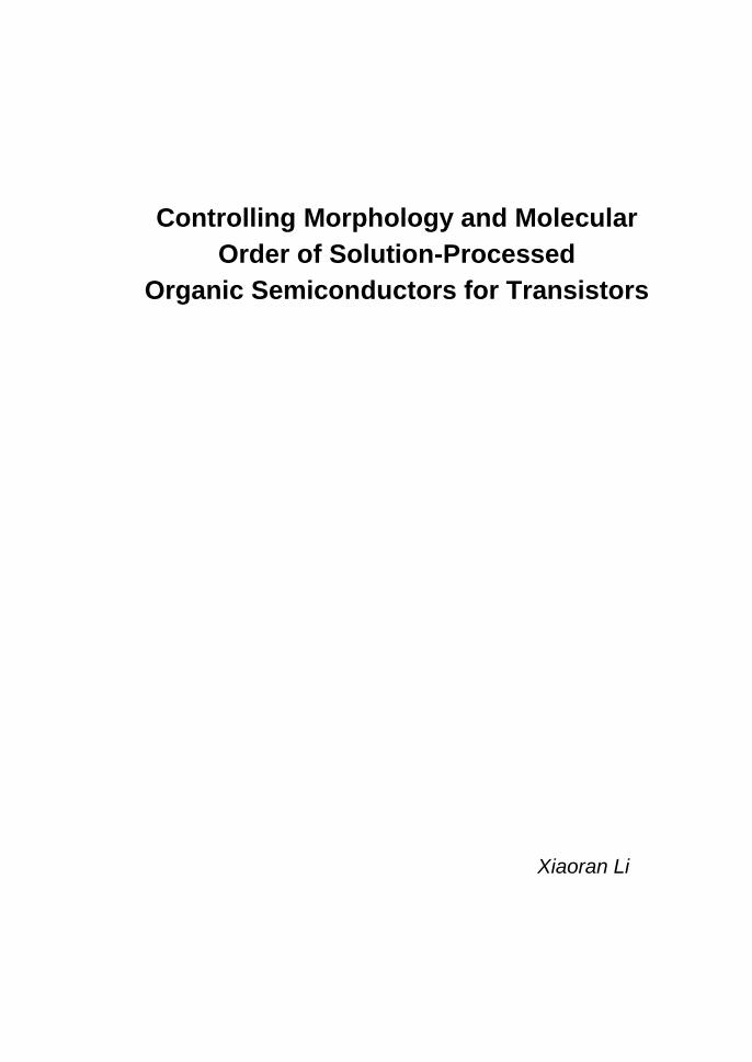
Cover design by Xiaoran Li
Front cover: an optical micrograph (dimensions of 250 μm by 250 μm, taken with
dark-field illumination) presents a peculiar morphology of tri-isopropylsilylethynyl
pentacene (TIPS-PEN) crystals, deposited by single-droplet ink-jet printing on a
gold-coated silicon wafer substrate. The contrast in this image comes from the light
scattered by TIPS-PEN microcrystallites, and mimics a walking 'pelican'.
Back cover: an optical micrograph (taken under crossed polarizers) shows a circular
array of 24 organic thin-film transistors, with the 'umbrella' shaped source and drain
electrodes made of gold, and a channel length of 40 μm.
Controlling Morphology and Molecular
Order of Solution-Processed
Organic Semiconductors for Transistors
PROEFSCHRIFT
ter verkrijging van de graad van doctor aan de
Technische Universiteit Eindhoven, op gezag van de
rector magnificus, prof.dr.ir. C.J. van Duijn, voor een
commissie aangewezen door het College voor
Promoties in het openbaar te verdedigen
op maandag 24 september 2012 om 16.00 uur
door
Xiaoran Li
geboren te Heilongjiang, China
Dit proefschrift is goedgekeurd door de promotor:
prof.dr. D.J. Broer
Copromotoren:
prof.dr.ing. C.W.M Bastiaansen
en
dr. G.H. Gelinck
A catalogue record is available from the Eindhoven University of Technology Library
ISBN: 978-90-386-3191-2
Printed by Ipskamp Drukkers, The Netherlands
Copyright © 2012 by Xiaoran Li

i
Contents
Contents ....................................................................................................................... i
1. Introduction............................................................................................................. 1
1.1 Background and motivation ................................................................................ 2
1.2 Molecular order and morphology control of organic semiconductors ................ 3
1.2.1 Tuning molecular order by molecular design .............................................. 4
1.2.2 Manipulation of morphology through controlled deposition from solution ... 6
1.3 Organic field-effect transistors.......................................................................... 10
1.3.1 Self-assembled monolayer transistors ...................................................... 11
1.3.2 Light-emitting & ferroelectric transistors .................................................... 13
1.4 Scope and outline of the thesis ........................................................................ 14
1.5 References ....................................................................................................... 17
2. Azeotropic binary solvent mixtures for preparation of organic single-crystal
transistors ................................................................................................................. 23
2.1 Introduction ....................................................................................................... 24
2.2 Experimental..................................................................................................... 25
2.3 Azeotropic mixture of isopropanol/toluene binary solvents .............................. 26
2.4 Morphology transition at azeotropic point & single-crystal formation ............... 27
ii
2.5 Characterizations of TIPS-PEN single crystals ................................................ 30
2.6 Single-crystal transistors & correlation of morphology with mobility ................ 31
2.7 Applicability to other π-conjugated molecules .................................................. 34
2.8 Conclusions ...................................................................................................... 36
2.9 References ....................................................................................................... 36
3. High-performance ink-jet printed single-droplet transistors based on a small
molecule/insulating polymer blend ........................................................................ 39
3.1 Introduction ....................................................................................................... 40
3.2 Experimental ..................................................................................................... 41
3.3 Impact of insulating polymer (PS) on transistor device performance ............... 42
3.4 Channel scaling studies .................................................................................... 46
3.5 Contact resistance identified by SKPM ............................................................ 48
3.6 Charge-trapping at the edges of Au electrodes in blend transistors ................ 50
3.7 On the relation between charge-trapping, threshold voltage & channel
conductivity ............................................................................................................. 51
3.8 Conclusions ...................................................................................................... 52
3.9 References ....................................................................................................... 52
4. Electric field confinement effect on charge transport in polycrystalline
organic field-effect transistors ................................................................................ 55
4.1 Introduction ....................................................................................................... 56
4.2 Experimental ..................................................................................................... 57
4.3 Results and discussions ................................................................................... 58
4.4 Conclusions ...................................................................................................... 63
4.5 References ....................................................................................................... 63
Appendix ................................................................................................................. 65
5. Solution-processed small molecule transistors with low operating voltages
and high grain-boundary anisotropy ...................................................................... 66
iii
5.1 Introduction ....................................................................................................... 67
5.2 Results and discussions ................................................................................... 68
5.3 Conclusions ...................................................................................................... 73
5.4 References ....................................................................................................... 73
6. Influence of solid-state microstructure on the electronic performance of a
small-molecule organic semiconductor ................................................................ 76
6.1 Introduction ....................................................................................................... 77
6.2 Experimental..................................................................................................... 78
6.3 Results and discussions ................................................................................... 79
6.4 Conclusions ...................................................................................................... 84
6.5 References ....................................................................................................... 85
7. n-type self-assembled monolayer field-effect transistors: towards self-
assembled complementary organic circuits ......................................................... 87
7.1 Introduction ....................................................................................................... 88
7.2 Experimental..................................................................................................... 89
7.3 Results and discussions ................................................................................... 90
7.4 Conclusions ...................................................................................................... 95
7.5 References ....................................................................................................... 96
8. Programmable polymer light emitting transistors with ferroelectric
polarization-enhanced channel current and light emission ................................ 98
8.1 Introduction ....................................................................................................... 99
8.2 Experimental..................................................................................................... 99
8.3 Opto-electrical characterizations & operation mechanism of ferroelectric
LEFETs ................................................................................................................. 100
8.4 Comparison between ferroelectric and non-ferroelectric LEFETs ................. 104
8.5 Programmability of ferroelectric LEFETs ....................................................... 106
8.6 Recombination zone in ferroelectric LEFETs ................................................. 107

iv
8.7 Numerical simulations for position of recombination zone & recombination
current ................................................................................................................... 108
8.8 Conclusions .................................................................................................... 110
8.9 References ..................................................................................................... 111
Summary ................................................................................................................. 113
List of Publications ................................................................................................ 117
Acknowledgements ................................................................................................ 120
Curriculum Vitae ..................................................................................................... 124

1
CHAPTER I
1. Introduction

Chapter 1
2
1.1 Background and motivation
Recent progress in organic electronics has brought several applications to
the market. Leading this trend are the flat-panel displays based on organic light-
emitting diodes (OLEDs) currently sold in stores (as shown in Figure 1.1a), and the
next-generation radio frequency identification (RFID) tags which could be attached
to virtually every commodity in supermarkets in the foreseeable future.
More specifically, as a potential low-cost alternative to traditional
amorphous-silicon based devices, organic field-effect transistors (OFETs) are now
of great research interest for the broad fields of information displays and
microelectronics, and expected to be ultimately incorporated into all-plastic
integrated circuits [1]
for rollable OLED display backplanes [2][3]
(Figure 1.1b), flexible
electrophoretic (e-ink) displays [4]
(Figure 1.1c), and flexible RFID tags [5]
(Figure
1.1d).
Figure 1.1 Representative applications of organic semiconductors in optical displays and
microelectronics. (a) LG Electronics: the world’s largest OLED HDTV presented at the 2012
Consumer Electronics Show (CES) in Las Vegas, it has a display size of 55 inches, weighs a
mere 7.5 kg and is only 4 mm thick [6]
. (b) Sony: a rollable full color 4.1 inches OLED display
driven by OFETs, being wrapped around a thin cylinder [7]
. (c) Polymer Vision: ‘Readius’, a
flexible electrophoretic (e-ink) display fabricated on plastic substrates using OFET backplanes [8]
. (d) PolyIC GmbH & Co. KG: roll-to-roll printing organic RFID tags on plastic substrates [9]
.
Over the last decade, breakthroughs have been made in the performance of
OFETs based on π-conjugated small-molecule organic semiconductors (OSCs) [10][11]
. Among them, tri-isopropylsilylethynyl pentacene (TIPS-PEN) and its
derivatives have been under extensive investigation, given their good charge-
Introduction
3
transport properties combined with decent air-stability, as well as the possibility of
inexpensive solution-processing at relatively low temperatures [12][13]
.
Controlling the growth and morphology of small-molecule and/or polymeric
OSCs is the key to achieve optimal performance for various organic optoelectronic
devices such as OFETs [14]
, OLEDs [15]
, and solar cells [16]
. Structural inhomogeneity
within a single component [17]
or between phase-separated blends [18]
has a
significant impact on the charge-transport properties [19][20]
, current densities [21]
, and
exciton related processes [22]
, giving rise to a certain spread of the local properties.
This spread leads to performance variation from one functional device to another,
and therefore hampers the practical applications of numerous devices integrated in
large areas. For instance, any non-uniformity in charge-carrier mobility and/or on-set
voltage of the driving transistors will potentially result in significant variations of pixel
luminance in an active-matrix OLED display. Apparently, to effectively integrate
individual OFETs onto OLED display backplanes over entire circuitry matrix, the
spread of device parameters for these OFETs (typically thousands to millions of)
should be minimized [1][4][23]
.
To this end, motivated by the practical applications of OFETs, currently in
both academic and industrial domains, unremitting efforts have been undertaken to
establish an ultimate control of morphology and molecular order for small-molecule
and/or polymeric OSCs. The objective is to improve device performance, yield, and
uniformity over large areas. This will continue to be one of the prerequisites for the
commercial success of organic electronics.
1.2 Molecular order and morphology control of organic
semiconductors
Organic semiconductors refer to a group of π-conjugated small molecules or
polymers. They comprise alternating single and double (carbon-carbon) bonds in
their molecular/polymeric backbones. This conjugation forms a so-called ‘π orbital’
providing a mutual overlap of the neighboring pz electrons. These ‘π-electrons’ are
delocalized in space (and energy) and therefore can move (freely) along the
conjugated backbone within an individual molecule (or polymer chain) through this
so-called electron ‘cloud’. More importantly, these delocalized π-electrons can also
travel from one molecule (or chain) to another via their shared electron ‘clouds’. The
probability and efficiency of this inter-molecular/inter-chain charge-transfer are
cooperatively determined by the amplitudes of ‘transfer integral’ (the extent of π-
orbital overlaps) and the ‘reorganization energy’ (energy consumption/loss during
electron transfer/exchange), between the adjacent molecules or polymer chains [24]
,
according to quantum-chemical calculations [25][26][27]
. In general, the higher the
transfer integral and the lower the reorganization energy, the faster exchange of
electrons between adjacent molecules would be, and the higher the charge-carrier
mobility of the material is expected to be [24][28][29][30]
.
Chapter 1
4
1.2.1 Tuning molecular order by molecular design
Since the charge-carrier transport in π-conjugated OSCs is taking place
along the overlapped intra- and inter-molecular π orbitals, the degree of overlap
between neighboring π orbitals will essentially determine the intrinsic charge-carrier
mobility of the semiconductor [31]
. Or translated to the molecular length scales, the
way how the adjacent molecules are organized (packed) in the solid state is
dominating the device mobility of an OSC [27]
.
Si
Si
(b)
Si
Si
S
S
(c)(a)
2
3
45678
114131211
10
9
Si
Si
(b)
Si
Si
Si
Si
(b)
Si
Si
S
S
(c)
Si
Si
S
S
Si
Si
S
S
(c)(a)
2
3
45678
114131211
10
9
(a)
2
3
45678
114131211
10
9
2
3
45678
114131211
10
9
2
3
2
3
45678 45678
114131211 114131211
10
9
10
9
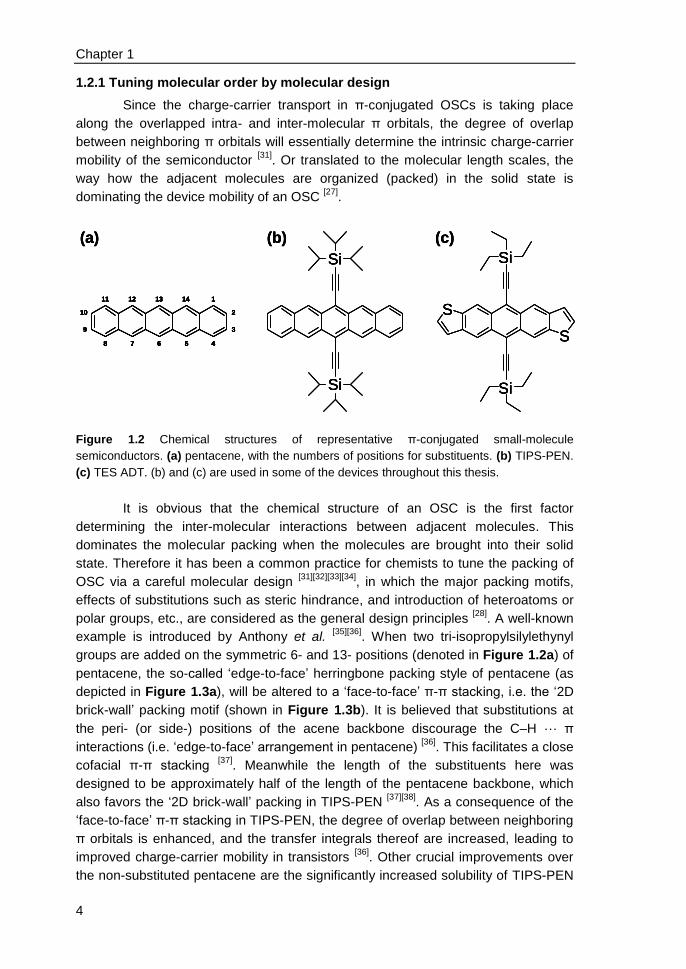
Figure 1.2 Chemical structures of representative π-conjugated small-molecule
semiconductors. (a) pentacene, with the numbers of positions for substituents. (b) TIPS-PEN.
(c) TES ADT. (b) and (c) are used in some of the devices throughout this thesis.
It is obvious that the chemical structure of an OSC is the first factor
determining the inter-molecular interactions between adjacent molecules. This
dominates the molecular packing when the molecules are brought into their solid
state. Therefore it has been a common practice for chemists to tune the packing of
OSC via a careful molecular design [31][32][33][34]
, in which the major packing motifs,
effects of substitutions such as steric hindrance, and introduction of heteroatoms or
polar groups, etc., are considered as the general design principles [28]
. A well-known
example is introduced by Anthony et al. [35][36]
. When two tri-isopropylsilylethynyl
groups are added on the symmetric 6- and 13- positions (denoted in Figure 1.2a) of
pentacene, the so-called ‘edge-to-face’ herringbone packing style of pentacene (as
depicted in Figure 1.3a), will be altered to a ‘face-to-face’ π-π stacking, i.e. the ‘2D
brick-wall’ packing motif (shown in Figure 1.3b). It is believed that substitutions at
the peri- (or side-) positions of the acene backbone discourage the C–H ··· π
interactions (i.e. ‘edge-to-face’ arrangement in pentacene) [36]
. This facilitates a close
cofacial π-π stacking [37]
. Meanwhile the length of the substituents here was
designed to be approximately half of the length of the pentacene backbone, which
also favors the ‘2D brick-wall’ packing in TIPS-PEN [37][38]
. As a consequence of the
‘face-to-face’ π-π stacking in TIPS-PEN, the degree of overlap between neighboring
π orbitals is enhanced, and the transfer integrals thereof are increased, leading to
improved charge-carrier mobility in transistors [36]
. Other crucial improvements over
the non-substituted pentacene are the significantly increased solubility of TIPS-PEN
Introduction
5
in common organic solvents, and a better environmental stability for the active
pentacene backbone, both properties are introduced by the bulky substituents [11][35][38]
. Apparently, the improved mobility, solubility, and stability of TIPS-PEN,
provide all desired properties for device applications. Therefore, TIPS-PEN is
regarded very promising for use in solution-processed OFETs, for high-throughput
and large-area productions of organic electronics. This possibility is also reflected by
the fact that TIPS-PEN is currently commercially available from many major
chemical companies around the world, e.g. Sigma-Aldrich, Merck, 3M, and Flexink.
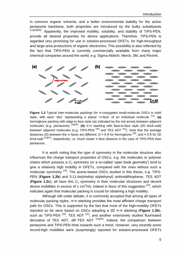
≈ 6Å≈ 3Å
(b)(a)
≈ 6Å
edge-to-face
≈ 6Å≈ 3Å
(b)
≈ 6Å≈ 3Å≈ 3Å≈ 3Å
(b)(a)
≈ 6Å
edge-to-face
(a)
≈ 6Å≈ 6Å≈ 6Å
edge-to-face
Figure 1.3 Typical inter-molecular packings for π-conjugated small-molecule OSCs in solid
state, with each ‘disc’ representing a planar ‘π-face’ of an individual molecule [12]
. (a)
herringbone packing with edge-to-face style (as indicated by the red arrow) between adjacent
molecules (e.g. pentacene) [39][40]
. (b) π-π stacking with face-to-face style (2D brick-wall)
between adjacent molecules (e.g. TIPS-PEN [35]
and TES ADT [41]
). Note that the average
distances (D) between the π-faces are different: D ≈ 6 Å for herringbone [39]
, and ≈ 3 Å for 2D
brick-wall [35][41]
, respectively, i.e. much closer π-face distance in the case of TIPS-PEN than
pentacene.
It is worth noting that the type of symmetry in the molecular structure also
influences the charge transport properties of OSCs, e.g. the molecules or polymer
chains which possess a C2 symmetry (or a so-called ‘open book geometry’) tend to
give a relatively high mobility in OFETs, compared with the ones without such a
molecular symmetry [24]
. The acene-based OSCs studied in this thesis, e.g. TIPS-
PEN (Figure 1.2b) and 5,11-bis(triethyl silylethynyl) anthradithiophene, TES ADT
(Figure 1.2c), all have this C2 symmetry in their molecular structures and decent
device mobilities in excess of 1 cm2/Vs, indeed in favor of this suggestion
[24], which
indicates again that molecular packing is crucial for obtaining a high mobility.
Although still under debate, it is commonly accepted that among all types of
molecular packing styles, π-π stacking provides the most efficient charge transport
path for OSCs. This is supported by the fact that most of the high-mobility OFETs
reported so far were based on OSCs adopting a 2D π-π stacking (Figure 1.3b),
such as TIPS-PEN [35]
, TES ADT [41]
, and another extensively studied fluorinated
derivative of TES ADT, diF-TES ADT [42][43]
. Indeed, the comparison between
pentacene and TIPS-PEN hints towards such a trend. However, very recently some
record-high mobilities were (surprisingly) reported for solution-processed OFETs
Chapter 1
6
using a group of thienoacene-based molecules [44]
with ‘herringbone-like’ type
molecular packing [45]
, such as the benzothieno[3,2-b]benzothiophene derivatives
(Cn-BTBT and DPh-BTBT) [46][45][47][48]
, and dibenzo[d,d']thieno[3,2-b;4,5-
b']dithiophene (DBTDT) [49][50]
. The high device mobilities (typically above 1 cm2/Vs)
and decent air-stability of Cn-BTBTs were attributed to a cooperative inter-molecular
interactions consisting of a ‘herringbone-like’ (C–H ··· π) interaction, a sulfur–sulfur
interaction, and a hydrophobic interaction induced by the long alkyl chains [45]
. These
comprehensive inter-molecular interactions substantially enhance the inter-
molecular overlaps of the ‘π-electron clouds’ and thereof significantly improve the
charge transport properties of this type of thienoacene-based OSCs [44]
.
Furthermore, recalling pentacene, the benchmark OSC material to date with
typical herringbone-packing style (Figure 1.3a), it is intriguing that upon device
optimizations an average transistor mobility well above 1 cm2/Vs was already
reported [51][52]
, let alone single-crystalline pentacene reaching a mobility as high as
40 cm2/Vs
[53].
To date, there is no definite answer to what kind of chemical structure with
which type of molecular packing (e.g. herringbone or π-π stacking) would result in
an intrinsic high-mobility OSC [28][54][55][56][57]
. Apparently a complex interplay between
all factors is taking place, and therefore it is far from trivial to improve the device
performance of OSCs solely by the approach of molecular design. Next, the
manipulation of morphology and molecular order of OSCs by various controlled
deposition methods (from solution phase) will be discussed.
1.2.2 Manipulation of morphology through controlled deposition from solution
The morphology of small-molecule crystalline OSC material, in a
macroscopic view, is how the crystals appear after deposition, visible to the naked
eyes on length scales of millimeters to centimeters. On the other hand, the
microscopic definition of the morphology deals with the degree of crystallinity, the
texture (shape, size, thickness) and directionality of the crystallites, the types of
crystal packing and lattice system, and the extent of crystal defect (structure
disorder or chemical impurity, etc.), typically on the scale of nanometer to
micrometer range. These macro- and micro-structures are inherently correlated and
have an immediate impact on the charge transport properties of OSCs [56][57][58]
.
Therefore, the structure-property relationships are of paramount importance for the
performance optimizations of OFETs [14][55]
.
To a large extent, the morphology of OSCs is determined by the way they
are deposited. Nowadays three major deposition methods are available for
controlled depositions of OSCs: (i) traditionally widely used thermal (vacuum)
evaporation (for thin-film formation) or physical vapor transport (for singe-crystal
formation); (ii) currently extensively exploited solution-based processes; and (iii)
recently reported solid-state (solvent-free) processes by compression-molding [59]
or
friction-transfer [60]
. Among them solution-based processes offer several advantages
such as being more efficient, low-temperature adaptable, and potentially
Introduction
7
inexpensive and easily tunable. They are therefore highly promising for high-
throughput and large-area mass production of organic electronics. Over the past
decade numerous solution-based deposition methods have been introduced and
frequently reviewed [28][61][62][63]
.
In general, the following processing factors cooperatively determine the final
morphology of solution-deposited OSCs: (i) the nature of the solution (temperature,
solute concentration, solubility of the solute, boiling point, polarity, surface tension
and viscosity of the solvent or solvent mixture, etc.); (ii) the deposition technique
(drop-cast [64]
, spin-coat [65]
, ink-jet print [66]
, spray-coat [67]
, dip-coat [68]
, zone-cast [69]
,
doctor-blade [41]
, solution-shear [70]
, wire-bar coat [71]
, micro-fluidic arrays [72]
, micro-
molding-in-capillaries [73]
, droplet-pinned crystallization [74]
, Langmuir-Blodgett
technique [75]
, and self-assembly from solution [76]
, etc.) and the processing
parameters therein (e.g. the speed/program for spin-coat), which provide different
drying speeds and/or unique fluid- and thermal- dynamics during solvent
evaporation; and (iii) the interactions between applied solution and the substrate
(temperature, surface energy, polarity, and roughness, etc.).
The as-cast films are often inhomogeneous or even noncontinuous. Post-
deposition methods such as solvent-vapor annealing [62][77][78]
and thermal annealing [79][80][81]
, are sometimes used to induce molecular order or improve uniformity of the
films.
Single-component organic semiconductors
As mentioned in previous sections, TIPS-PEN is currently regarded as a
model single-component OSC material for solution-processed OFETs, based on its
good solubility in common solvents, high charge-carrier mobility, and decent stability
in air [35][65][82][83]
. The morphology and structure-property relationships for TIPS-PEN
and its analogs have been summarized in literature [11][38]
, and various solution-
based methods for controlled depositions of this type of materials have also been
well documented [12][13][83]
. With optimized combination of above mentioned
processing parameters, four types of typical morphologies [64][66][84][85][86][87]
can be
found for solution-processed TIPS-PEN crystals: ribbon-like needles, various
shaped spherulites, big platelets, or parallelepiped-shaped single crystals with well-
defined crystal facets.
Single crystals
Given the advantage of absence of disorder or grain-boundary in organic
single crystals [88][89][90][91]
, it is generally believed that direct fabrication of single-
crystal OFETs from solution-phase is an effective route to achieve device
performance superior to the polycrystalline thin-film device. By making use of
the solubility difference for two solvents, a so-called ‘solvent-exchange’ method was
introduced to produce single-crystals of TIPS-PEN, in which a small volume of a
solution containing the TIPS-PEN molecules in a good solvent is injected into a large
Chapter 1
8
excess of a bad solvent, resulting in ribbon-like single crystals exhibiting mobilities of
up to 1.4 cm2/Vs in a bottom-gate/top-contact configuration
[87].
Very recently, a similar concept was used for a more ‘exotic’ ink-jet printing
method with a double print heads [46]
: First, a large number of droplets of a bad
solvent (or the so-called ‘antisolvent’) were ink-jet printed to fill up a pre-designed
protuberance-shaped reservoir. Then instantaneously, from a second print head, a
few droplets of a good solvent containing OSC molecules (C8-BTBT or TIPS-PEN)
were printed onto this confined liquid layer of the bad solvent, at a specific location
to induce a laminar flow of the microfluid. This led to a slowly moving front of crystal
growth and eventually single-crystal or single-crystal-like thin films deposited in the
designated area. Although no device data for TIPS-PEN was presented in this study,
the as-printed C8-BTBT single-crystal films displayed a maximum mobility as high as
31.3 cm2/Vs, a record value for Cn-BTBT based OFETs so far
[44][46].
Another recent example of single-crystal OFETs were fabricated by ink-jet
printing TIPS-PEN dissolved in a specific co-solvent mixture, and via a spatial
patterning of dewetting self-assembled monolayer by deep UV exposure to define
the nucleation sites for single-crystal growth. Finally, solvent-vapor annealing was
used to improve the device performance, where a highest mobility of 1.7 cm2/Vs was
achieved [92]
. These latest developments for controlled depositions of single-crystal
OFETs are indeed intriguing, and encouraging for further endeavors.
Uniaxially-aligned crystals
Meanwhile, several studies by electrical or optical approaches have
confirmed that charge transport in π-conjugated organic single crystals is, to a large
extent, dependent on their crystallographic direction: electrical measurements of
field-effect mobilities for rubrene single crystals grown by physical vapor transport
demonstrated that the mobility along the b-axis was a factor of 3.5 larger than in the
a-axis direction [93]
; transient photoconductivity measurements on TIPS-PEN single
crystals fabricated from solution exhibited almost the same anisotropy value [94]
.
Therefore, in an ideal device, all TIPS-PEN molecules between the source and drain
electrodes should form a ‘mono-domain’ arrangement with the major π-π stacking
axis parallel to the source-to-drain bias direction. This well-aligned crystallographic
direction has been demonstrated in various single-crystal OFETs to provide an
optimized charge-transport path and maximized device mobility [95][96][97]
.
Dip-coating has been proven effective to produce such a well-oriented
morphology, with long needles of TIPS-PEN uniaxially aligned along the source-to-
drain direction [68][98]
. Interestingly, on top of the in-grain anisotropy, the presence of
grain boundaries [68]
, high degree of molecular ‘misorientation’ at certain less
favorable grain boundaries with high crystallographic ‘misorientation’ (in the case of
‘2D brick-wall’ π-π packing such as TIPS-PEN) [17]
, and material voids [98]
within the
active channels, were all found additionally limiting the charge transport and highly
anisotropic, responsible for the observed large anisotropy of OFET mobilities.
Introduction
9
Zone-casting is a well-known technique to fabricate well-aligned films of
columnar discotic liquid-crystalline OSCs [69][99]
. More recently, a so-called ‘solution-
shearing’ method, comparable to zone-casting in its setup but conceptually more
close to the ‘doctor-blading’ [41]
, was introduced to produce uniaxially oriented
needles of TIPS-PEN [100]
and other small-molecule OSCs [70]
, with typical
morphologies very similar to the ones previously deposited by dip-coating [17][68][98]
.
However, the striking finding from Ref. [100]
is that the π-π stacking distance of TIPS-
PEN crystals can be fine-tuned (from 3.33 Å to 3.08 Å) by varying the solution-
shearing speed. This was explained by the incrementally introduced ‘lattice strain’ to
the strained films during solution-shearing. Apart from the well-known effects of
crystal size, orientation, and number of grain boundaries, it was also found that the
overall charge-transfer integrals may not necessarily increase with a shorter π-π
stacking distance, due to the molecular displacements along both the molecular long
and short axes, caused by the ‘lattice strain’ induced in the crystal packing. A
maximum transistor mobility of 4.6 cm2/Vs was measured in a bottom-gate/top-
contact configuration, sheared at an intermediate speed of 2.8 mm/s with a
moderate π-π stacking distance.
Last but not the least, it is worth noting that the above-mentioned methods
to uniaxially align OSCs from solution always obtain the best-performing OFET
devices at deposition speeds on the order of mm/s and even lower, at least 3 orders
of magnitude slower than the conventional industrial printing process. Consequently,
further development of more industrially viable deposition methods is considered as
the major step forward towards the commercial success of organic electronics.
Meanwhile it remains very challenging to translate the current knowledge gained
from research labs to future practical production lines.
Blending small molecules with polymers
As an alternative to single-component OFETs, blending the small-molecule
OSC with a polymer, is another effective approach to improve the morphology and
device performance of small-molecule-based OFETs [18]
. The molecular weight,
crystallinity, conductivity (semiconducting or insulating) of the blended polymer, the
choice of the solvent/co-solvent, and the blending ratio between small molecules
and polymers are usually the parameters of interest for device optimizations.
It is commonly believed that, upon casting and solvent evaporation, the
occurrence of a vertical stratification between the small-molecule OSC and blended
polymer plays a crucial role for the device performance of these blend transistors [18]
.
Under proper processing conditions, during solvent drying the small-molecule OSC
can be predominantly expelled to both the top (air) and bottom (substrate) interfaces
of the deposited blend film [101][102][103]
. Since the charge transport in OFETs takes
place within the zone of only a few nanometers away from the
semiconductor/dielectric interface [104]
, as long as this vertical phase stratification
results in an almost ‘pure’ phase of small-molecule OSC at the interface, high-
performance blend transistors would be achievable.

Chapter 1
10
Moreover, at least three mechanisms were recently proposed in literature for
the improved charge transport in blend transistors: (i) Ohe et al. explained that the
addition of the polymer binder results in a slower solvent drying and hence to an
improved film morphology and uniformity [102]
; (ii) Rivnay et al. suggested that, the
energetic barrier for charge transport across certain less-favorable grain boundaries
with high degree of molecular ‘misorientation’ (present in the neat small-molecule
OSC with a ‘2D brick-wall’ π-π packing), can be substantially reduced when a
semiconducting polymer is added, leading to an improved device performance [17]
;
and (iii) Yoon et al. proposed that blending an insulating polymer influences the film
formation process of the small-molecule OSC, and acts (indirectly) as a purification
method, the so-called ‘zone-refinement effect’ during solidification [105]
.
In line with optimizing the morphology of OSCs by blending, high resolution
characterization techniques are usually desired to obtain deeper understanding on
how the altered morphology relates to the charge-transport properties in devices, e.g.
the effects of induced vertical (or lateral) phase-separation. Electrical scanning
probe microscopy has been proven an effective tool to reveal such structure-
property relationships microscopically, on active layers of different types of devices [106][107][108]
, taking advantage of its ability to image topography simultaneously with
other surface properties at a typical resolution of 10-100 nm. In the case of OFETs,
scanning Kelvin probe (SKPM) [108][109][110][111]
and electric force microscopy (EFM) [107][112]
were extensively used to study the local charge-transport properties within
the transistor channels. Alternatively, conductive atomic force microscopy (C-AFM)
is a current sensing technique that monitors the variations in electrical conductivity
of materials and thus can reveal charge-transport paths and barriers [113][114][115][116]
.
These high resolution techniques are continuously serving as powerful tools for
probing the important dynamic interfaces of OFETs, and for better understanding the
structure-property relationships in organic electronics.
1.3 Organic field-effect transistors
In simple words, a transistor is an electronic switch with its ON- and OFF-
states modulated by the gate bias applied. In contrast to the ‘metal-oxide-
semiconductor field-effect transistors’ (MOSFETs) in which a so-called ‘inversion’
layer is formed during operation [117][118][119]
, organic field-effect transistors (OFETs)
are typically operating in the ‘accumulation’ mode [120][121][122][123]
. The working
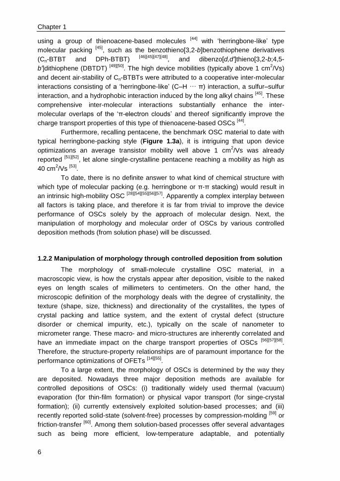
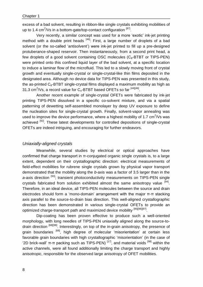
principle of an OFET, in a typical ‘bottom-gate/bottom-contact’ (BG/BC) device
configuration, is illustrated in Figure 1.4. When a voltage bias (VGS) is applied to the
gate electrode, charge carriers (with a polarity opposite to the gate bias) can be
injected from the source/drain electrodes and accumulated at the
semiconductor/dielectric interface, i.e. a conducting channel is induced by the gate.
Under a lateral source-drain bias (VDS), these gate-induced mobile charges will flow
laterally along the interface, i.e. a source-to-drain field-effect current (ISD) occurs and
the transistor is turned ‘ON’.
Introduction
11
VGS
VDS
Semiconductor
Source
Gate
Drain
Dielectric
ISD
VGS
VDS
Semiconductor
Source
Gate
Drain
Dielectric
ISD
Figure 1.4 Schematic illustration (cross-section view) for a p-type field-effect transistor in
operation, in a bottom-gate/bottom-contact (BG/BC) configuration. This device configuration is
used throughout this thesis (except for Chapter 8 where a top-gate/bottom-contact will be
adopted).
To date, the fundamental understandings on charge-transport mechanisms
of OSCs [27][30][124][125][126]
, detailed methods for device parameter extractions of
OFETs [10][127][128]
, full descriptions of energy level alignment and charge injection
process [129][130][131]
, and comprehensive analyses on device physics [91][132][133][134][135]
and interface engineering [136][137][138]
for organic thin-film and/or single-crystal
transistors, have been extensively reviewed in various literature.
Despite the differences in morphology, molecular order, and the level of
chemical purity in the active semiconducting layer, a mobility value in a specific
transistor device is actually a combined result of (i) device configuration (BG/BC,
TG/TC, BG/TC, TG/BC) and geometry (channel length/width, thickness of the
semiconductor layer); (ii) interfacial properties of the semiconductor/dielectric and
semiconductor/contact interfaces; (iii) energy level alignment at the
semiconductor/contact interfaces; and (iv) the dielectric constant [139]
and surface
polarity (influencing the density-of-states [140][141]
) of the dielectric layer. For instance,
it is generally believed that BG/TC and TG/BC configurations give a larger effective
surface area for charge injection from the source/drain contacts, leading to a lower
contact resistance, compared with the BG/BC or TG/TC devices, despite the fact
that the injected charges have to travel through the bulk of the semiconductor layer [136]
.
Clearly, the mobility in an OSC is a device-parameter rather than a material-
parameter (sometimes even varies when the current-voltage sweeping speed is
different), therefore one should bear this in mind when comparing mobility values for
transistors produced in different device architectures, or measured under different
conditions, etc..
1.3.1 Self-assembled monolayer transistors
As an alternative to the ‘conventional’ solution-based processes described
above, the idea of fabricating OFETs in which the active semiconducting layer
consists of a monolayer of the molecules spontaneously self-assembled from
solution (i.e. without human intervention) is fascinating, and envisioned by many
researchers as the ‘holy grail’ for the so-called ‘bottom-up’ approach in molecular
electronics.
Chapter 1
12
Self-assembled monolayers (SAMs) are organic assemblies formed by the
chemisorption of molecular constituents from solution (or the gas phase) onto the
surface of a solid substance (substrate). The adsorbates can organize themselves
autonomously (and sometimes epitaxially) into crystalline (or semicrystalline)
structures [142]
. The functionality of a SAM can be chemically tailored by the
properties of its terminal group, which renders its versatility in many applications in
organic electronics [137]
: e.g. tuning the work-function of metals [143]
, patterning the
wetting properties of surfaces [144]
, and fabricating large-area molecular junctions [145]
or ultrathin nano-dielectrics for transistors [146]
. However, only a few studies on the
use of SAM as the active charge-transport layer in field-effect transistors (SAM-
based FETs, namely SAMFETs) were initially reported [147][148][149]
.
Only recently, a quinquethiophene functionalized monochlorosilane, with a
π-conjugated mesogenic core and a long aliphatic chain as the spacer, was found to
form well-ordered semiconducting SAMs on SiO2 or polymer surfaces. The
SAMFETs fabricated thereof were proven highly effective to produce reliable
integrated circuits with large-area uniformity [150][151][152]
.
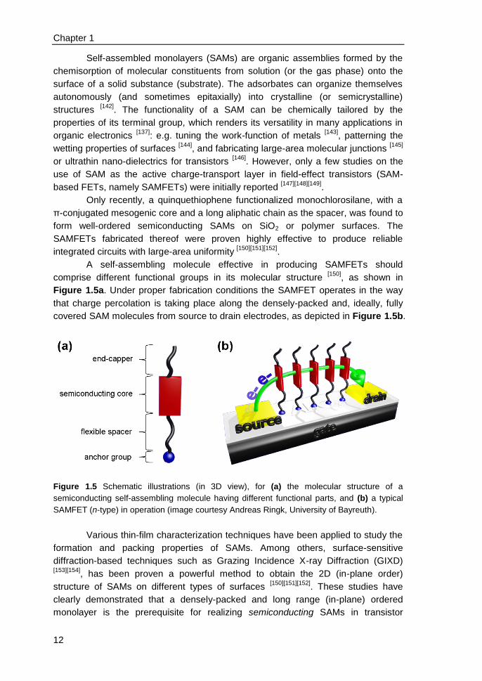
A self-assembling molecule effective in producing SAMFETs should
comprise different functional groups in its molecular structure [150]
, as shown in
Figure 1.5a. Under proper fabrication conditions the SAMFET operates in the way
that charge percolation is taking place along the densely-packed and, ideally, fully
covered SAM molecules from source to drain electrodes, as depicted in Figure 1.5b.
Figure 1.5 Schematic illustrations (in 3D view), for (a) the molecular structure of a
semiconducting self-assembling molecule having different functional parts, and (b) a typical
SAMFET (n-type) in operation (image courtesy Andreas Ringk, University of Bayreuth).
Various thin-film characterization techniques have been applied to study the
formation and packing properties of SAMs. Among others, surface-sensitive
diffraction-based techniques such as Grazing Incidence X-ray Diffraction (GIXD) [153][154]
, has been proven a powerful method to obtain the 2D (in-plane order)
structure of SAMs on different types of surfaces [150][151][152]
. These studies have
clearly demonstrated that a densely-packed and long range (in-plane) ordered
monolayer is the prerequisite for realizing semiconducting SAMs in transistor
Introduction
13
devices with good reproducibility [150][151]
. The mobility of p-type SAMFETs reported
so far was on the order of 10-2
cm2/Vs, most likely limited by the intrinsic low mobility
of the semiconducting cores (e.g. α-substituted quinquethiophene in Refs [150][151][152]
)
of the SAM molecules studied [138]
. However, it is not trivial to introduce high-mobility
semiconducting units (e.g. with strong π-π stacking motifs) into the SAM molecule
without compromising the capability of these molecules to self-assemble [155][156]
, or
bringing about stability issues throughout the complex synthetic routes. Moreover, to
date a highly reproducible n-type SAMFET is still missing [155][156]
, and this hampers
the further advancement of SAMFETs into a complementary logic.
1.3.2 Light-emitting & ferroelectric transistors
Apart from acting as a conventional electronic switch, when a specific
semiconductor or dielectric layer is chosen, additional functionality can be
implemented to an OFET, such as light emission or memory effects.
Recent realization of ambipolar charge-transport in OFETs [157] has enabled
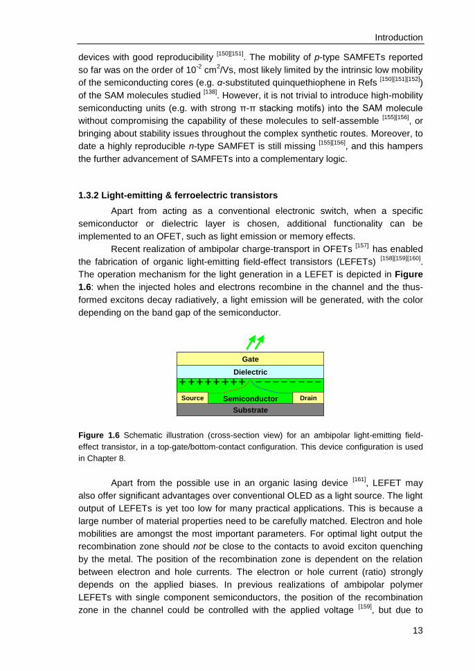
the fabrication of organic light-emitting field-effect transistors (LEFETs) [158][159][160].
The operation mechanism for the light generation in a LEFET is depicted in Figure
1.6: when the injected holes and electrons recombine in the channel and the thus-
formed excitons decay radiatively, a light emission will be generated, with the color
depending on the band gap of the semiconductor.
Dielectric
Semiconductor
Substrate
Drain
Gate
Source
Dielectric
Semiconductor
Substrate
Drain
Gate
Source
Figure 1.6 Schematic illustration (cross-section view) for an ambipolar light-emitting field-
effect transistor, in a top-gate/bottom-contact configuration. This device configuration is used
in Chapter 8.
Apart from the possible use in an organic lasing device [161]
, LEFET may
also offer significant advantages over conventional OLED as a light source. The light
output of LEFETs is yet too low for many practical applications. This is because a
large number of material properties need to be carefully matched. Electron and hole
mobilities are amongst the most important parameters. For optimal light output the
recombination zone should not be close to the contacts to avoid exciton quenching
by the metal. The position of the recombination zone is dependent on the relation
between electron and hole currents. The electron or hole current (ratio) strongly
depends on the applied biases. In previous realizations of ambipolar polymer
LEFETs with single component semiconductors, the position of the recombination
zone in the channel could be controlled with the applied voltage [159]
, but due to
Chapter 1
14
device variability it is still very challenging to fabricate LEFETs with the
recombination zone at a controlled and fixed position. A ‘pinned’ recombination zone
will open the way to integrate specific optical out-coupling structures in the channels
of these LEFETs to further increase the brightness, together with the possibility of
increased current densities, this may help to reach population inversion which is a
prerequisite for an electrically driven organic laser.
Over the past few years, a number of optoelectronic devices have been
explored in which OSCs were combined with ferroelectric materials [162]
, including
OFETs [163]
, OLEDs [164]
, and solar cells [165][166][167]
. The use of the ferroelectric
polarization field in these devices has allowed for an extremely large modulation of
the charge-carrier density and electronic properties of the OSCs [163][168]
.
Semiconductor
Substrate
Gate
Source Drain
Ferroelectric
(b)(a)
Semiconductor
Substrate
Gate
Source Drain
Dielectric (non-ferroelectric)
Semiconductor
Substrate
Gate
Source Drain
Ferroelectric
(b)
Semiconductor
Substrate
Gate
Source Drain
Ferroelectric
Semiconductor
Substrate
Gate
Source DrainSemiconductor
Substrate
Gate
Source Drain
Ferroelectric
(b)(a)
Semiconductor
Substrate
Gate
Source Drain
Dielectric (non-ferroelectric)
(a)
Semiconductor
Substrate
Gate
Source Drain
Dielectric (non-ferroelectric)
Semiconductor
Substrate
Gate
Source Drain
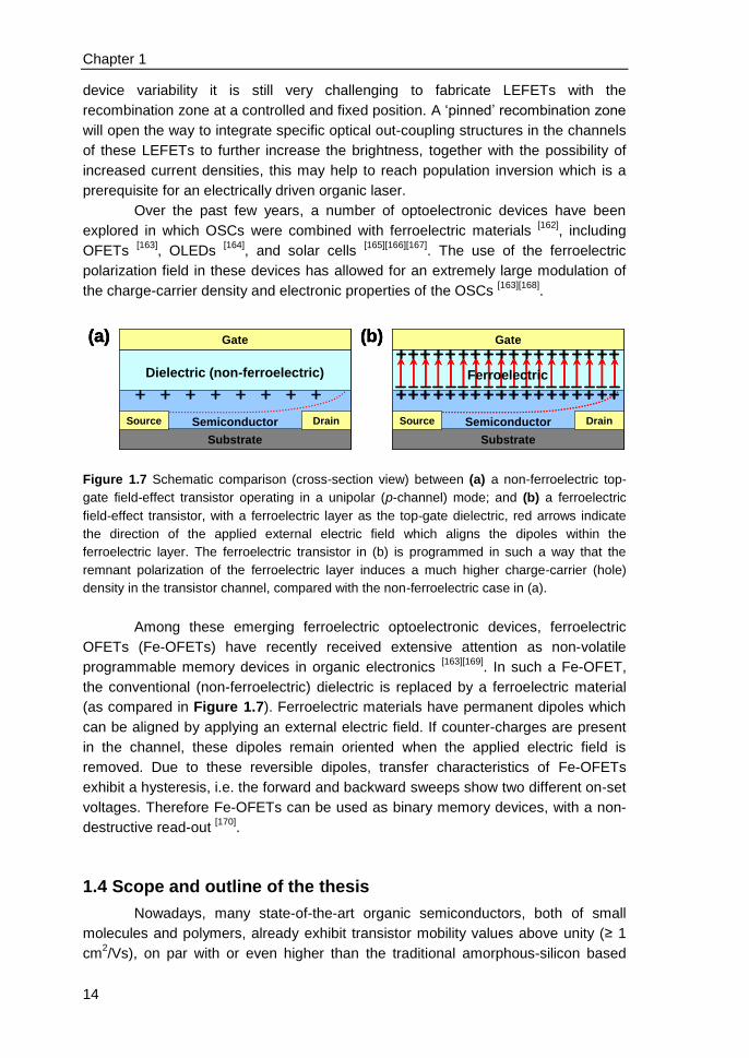
Dielectric (non-ferroelectric)
Figure 1.7 Schematic comparison (cross-section view) between (a) a non-ferroelectric top-
gate field-effect transistor operating in a unipolar (p-channel) mode; and (b) a ferroelectric
field-effect transistor, with a ferroelectric layer as the top-gate dielectric, red arrows indicate
the direction of the applied external electric field which aligns the dipoles within the
ferroelectric layer. The ferroelectric transistor in (b) is programmed in such a way that the
remnant polarization of the ferroelectric layer induces a much higher charge-carrier (hole)
density in the transistor channel, compared with the non-ferroelectric case in (a).
Among these emerging ferroelectric optoelectronic devices, ferroelectric
OFETs (Fe-OFETs) have recently received extensive attention as non-volatile
programmable memory devices in organic electronics [163][169]
. In such a Fe-OFET,
the conventional (non-ferroelectric) dielectric is replaced by a ferroelectric material
(as compared in Figure 1.7). Ferroelectric materials have permanent dipoles which
can be aligned by applying an external electric field. If counter-charges are present
in the channel, these dipoles remain oriented when the applied electric field is
removed. Due to these reversible dipoles, transfer characteristics of Fe-OFETs
exhibit a hysteresis, i.e. the forward and backward sweeps show two different on-set
voltages. Therefore Fe-OFETs can be used as binary memory devices, with a non-
destructive read-out [170]
.
1.4 Scope and outline of the thesis
Nowadays, many state-of-the-art organic semiconductors, both of small
molecules and polymers, already exhibit transistor mobility values above unity (≥ 1
cm2/Vs), on par with or even higher than the traditional amorphous-silicon based
Introduction
15
devices [122]
. In this respect the work presented in this thesis is not aiming to produce
record-mobility transistors. Instead, we aimed to achieve highly reproducible organic
transistors, with device parameters relevant to practical applications (e.g. relatively
low operating-voltages and steep sub-threshold slopes, uniform performance in
large areas), through controlling the morphology and molecular order of small-
molecule organic semiconductors. We restricted ourselves on fabrication
technologies based on solution-process compatible with high-throughput production
(e.g. simpler method with reduced processing steps and at high device yield).
Meanwhile we studied the microstructure evolution of these materials deposited
using different methods, and its impact on the charge-transport properties in
transistors.
To control the morphology and molecular order of organic semiconductors,
this thesis is taking the following two approaches: via developing and optimizing
solution-based deposition methods, and/or by an educated molecular design. The
following research questions will be addressed during the course of this thesis:
(1): Can we produce organic single-crystal transistors by a single-step solution
process?
(2): Would the blending of a small-molecule organic semiconductor with an
insulating polymer result in an improvement in device performance for ink-jet printed
organic transistors? And what is the role of the blended polymer on the device
operation?
(3): What is the role of the grain boundaries in the lateral-field dependence of
charge-carrier mobility in polycrystalline organic transistors?
(4): Would the effect of alkyl substitutions at the end-positions of the pentacene
backbone of TIPS-PEN be positive, in terms of transistor performance?
(5): Would the device performance and reproducibility of an acene derivative (TES
ADT) be improved, solely by a careful selection of the casting temperature?
(6): Is long range in-plane order still the prerequisite for a semiconducting self-
assembled monolayer for use in field-effect transistor? And can we produce a self-
assembled complementary circuit, based on the highly selective nature of p- or n-
type self-assembling molecules with different anchoring groups covalently bonded to
the respective dielectric surfaces?
(7): Is it possible to enhance the light output and device efficiency of a light-emitting
organic transistor by using a ferroelectric polymer as the gate dielectric? And would
there be any additional functionality in such a ferroelectric light-emitting transistor?
We start from Chapter 2 by controlling (solely) the solvent parameters
during deposition. By using the concept of azeotropism for the first time, a single-
step solution process is introduced to prepare large single crystals of TIPS-PEN
from a binary solvent mixture. Then we characterize these single crystals in terms of
transistor performance and present a direct correlation between crystal morphology
and device mobility.
Chapter 1
16
In Chapter 3 we present a systematic study of the influence of material
composition and ink-jet processing conditions on the charge transport in OFETs
based on single droplets of TIPS-PEN/polystyrene blends. After careful process
optimization of blending ratio and printing temperature, we routinely make blend
transistors superior to the neat TIPS-PEN devices. Using channel scaling
measurements and scanning Kelvin probe microscopy, we try to understand the
charge transport and device operation of our blend transistors, systematically
compared with the neat TIPS-PEN devices.
While it is known that the charge-carrier mobility in organic semiconductors
is only weakly dependent on the electric field at low fields, in Chapter 4 of this thesis,
our experimental charge-carrier mobility in OFETs using TIPS-PEN is found to be
surprisingly field-dependent at low source-drain fields. Corroborated by scanning
Kelvin probe measurements, we explain this experimental observation by the severe
difference between the local lateral-field dependences within grains and at grain
boundaries. The role of grain boundaries will be explained and highlighted.
Chapter 5 presents a new TIPS-PEN derivative, namely BTE-TIPS-PEN,
with ethyl substituents at the 2,3,9,10 backbone positions to modulate the solubility
and film-forming properties. We will demonstrate that, an improved molecular design
can indeed result in a controlled macro- and micro-structure of OSC thin films that
positively influences their device performance.
Next, we will show in Chapter 6, that a careful selection of the casting
temperature alone can allow a rapid production of OFETs with uniform and
reproducible device performance over large areas. We will present four distinctive
solid-state phases of TES ADT exhibiting drastically different charge-transport
properties, deduced from OFET device characteristics corroborated by Lateral Time-
of-Flight (L-ToF) photoconductivity measurements. The best-performing crystal
polymorph of TES ADT is identified.
In Chapter 7 we present the first highly-reproducible n-type SAMFET, based
on a perylene derivative (namely PBI-PA) with a phosphonic acid anchoring group
which enables an efficient fixation to aluminum oxide. We will show that, despite the
lack of long range in-plane order in the monolayer, our PBI-PA SAMFETs still exhibit
decent electron mobilities. By implementing p- and n-type SAMFETs in one circuit, a
complementary inverter based solely on SAMFETs is demonstrated for the first time.
In the last Chapter, we will introduce an unconventional use of the molecular
(polymer chain/dipole) alignment, in the dielectric layer of organic field-effect
transistors. Chapter 8 presents a voltage-programmable light-emitting field-effect
transistor (LEFET) using a ferroelectric polymer as the gate dielectric. The role of
ferroelectric poling (dipole alignment) on the device operation and functionality will
be highlighted.
Introduction
17
1.5 References
[1] H.E.A. Huitema, G.H. Gelinck, J.B.P.H. van der Putten, K.E. Kuijk, C.M. Hart, E. Cantatore, P.T. Herwig, A.J.J.M. van Breemen, D.M. de Leeuw, Nature 2001, 414, 599.
[2] M. Noda, N. Kobayashi, M. Katsuhara, A. Yumoto, S. Ushikura, R. Yasuda, N. Hirai, G. Yukawa, I. Yagi, K. Nomoto, T. Urabe, J. Soc. Info. Display 2011, 19, 316.
[3] K. Nomoto, M. Noda, N. Kobayashi, M. Katsuhara, A. Yumoto, S. Ushikura, R. Yasuda, N. Hirai, G. Yukawa, I. Yagi, SID Symp. Digest 2011, 42, 488.
[4] G.H. Gelinck, H.E.A. Huitema, E. van Veenendaal, E. Cantatore, L. Schrijnemakers, J.B.P.H. van der Putten, T.C.T. Geuns, M. Beenhakkers, J.B. Giesbers, B.-H. Huisman, E.J. Meijer, E.M. Benito, F.J. Touwslager, A.W. Marsman, B.J.E. van Rens, D.M. de Leeuw, Nat. Mater. 2004, 3, 106–110.
[5] E. Cantatore, T.C.T. Geuns, G.H. Gelinck, E. van Veenendaal, A.F.A. Gruijthuijsen, L. Schrijnemakers, S. Drews, D.M. de Leeuw, IEEE J. Solid-State Circuits 2007, 42, 84–92.
[6] LG Electronics: 55-inch OLED TV, 2012, http://www.bgr.com/2012/01/13/ces-2012-rundown-new-tv-tech-excites-tablets-are-toast/.
[7] Sony: Rollable OFET-driven OLED Display, 2010, http://www.sony.net/SonyInfo/News/Press/201005/10-070E/.
[8] Polymer Vision: ‘Readius’ Flexible Display Using OFET Backplanes, 2008, http://www.phonesreview.co.uk/2008/02/04/readius-e-ink-phone-from-polymer-vision-coming-mid-2008-in-italy/.
[9] PolyIC: Roll-to-roll Printed Organic RFID Tags, 2006, http://www.polyic.com/press-images.php (accessed on 20th March 2012).
[10] D. Braga, G. Horowitz, Adv. Mater. 2009, 21, 1473–1486. [11] J. Anthony, Angew. Chem. Int. Ed. 2008, 47, 452–483. [12] J.A. Lim, H.S. Lee, W.H. Lee, K. Cho, Adv. Funct. Mater. 2009, 19, 1515–
1525. [13] S. Liu, W.M. Wang, A.L. Briseno, S.C.B. Mannsfeld, Z. Bao, Adv. Mater.
2009, 21, 1217–1232. [14] A. Virkar, S. Mannsfeld, Z. Bao, N. Stingelin, Adv. Mater. 2010, 22, 3857–
3875. [15] Y. Shi, J. Liu, Y. Yang, J. Appl. Phys. 2000, 87, 4254–4263. [16] A. Moule, K. Meerholz, Adv. Funct. Mater. 2009, 19, 3028–3036. [17] J. Rivnay, L.H. Jimison, J.E. Northrup, M.F. Toney, R. Noriega, S. Lu, T.J.
Marks, A. Facchetti, A. Salleo, Nat. Mater. 2009, 8, 952–958. [18] J. Smith, R. Hamilton, I. McCulloch, N. Stingelin-Stutzmann, M. Heeney, D.
Bradley, T. Anthopoulos, J. Mater. Chem. 2010, 20, 2562–2574. [19] R.J. Kline, M.D. McGehee, E.N. Kadnikova, J. Liu, J.M.J. Fréchet, M.F.
Toney, Macromolecules 2005, 38, 3312–3319. [20] C. McNeill, K. Asadi, B. Watts, P. Blom, D. de Leeuw, Small 2010, 6, 508–
512. [21] J. Zaumseil, R. Kline, H. Sirringhaus, Appl. Phys. Lett. 2008, 92, 073304. [22] F. Spano, Annu. Rev. Phys. Chem. 2006, 57, 217–243. [23] H.E.A. Huitema, G.H. Gelinck, J.B.P.H. van der Putten, K.E. Kuijk, C.M. Hart,
E. Cantatore, D.M. de Leeuw, Adv. Mater. 2002, 14, 1201–1204. [24] M. He, J. Li, A. Tandia, M. Sorensen, F. Zhang, H.H. Fong, V.A. Pozdin, D.-
M. Smilgies, G.G. Malliaras, Chem. Mater. 2010, 22, 2770–2779. [25] J.L. Brédas, J.P. Calbert, D.A. Da Silva Filho, J. Cornil, Proc. Natl. Acad. Sci.
USA 2002, 99, 5804–5809. [26] R.A. Marcus, J. Chem. Phys. 1956, 24, 966–978.
Chapter 1
18
[27] V. Coropceanu, J. Cornil, D.A. da Silva Filho, Y. Olivier, R. Silbey, J.-L. Brédas, Chem. Rev. 2007, 107, 926–952.
[28] C. Wang, H. Dong, W. Hu, Y. Liu, D. Zhu, Chem. Rev. 2012, 112, 2208–2267.
[29] S.T. Bromley, M. Mas-Torrent, P. Hadley, C. Rovira, J. Am. Chem. Soc. 2004, 126, 6544–6545.
[30] J.-L. Brédas, D. Beljonne, V. Coropceanu, J. Cornil, Chem. Rev. 2004, 104, 4971–5004.
[31] H. Dong, C. Wang, W. Hu, Chem. Commun. 2010, 46, 5211–5222. [32] S. Allard, M. Forster, B. Souharce, H. Thiem, U. Scherf, Angew. Chem. Int.
Ed. 2008, 47, 4070–4098. [33] M. Gsänger, J.H. Oh, M. Könemann, H.W. Höffken, A. Krause, Z. Bao, F.
Würthner, Angew. Chem. Int. Ed. 2010, 49, 740–743. [34] C. Wang, H. Dong, H. Li, H. Zhao, Q. Meng, W. Hu, Cryst. Growth Des.
2010, 10, 4155–4160. [35] J.E. Anthony, J.S. Brooks, D.L. Eaton, S.R. Parkin, J. Am. Chem. Soc. 2001,
123, 9482–9483. [36] C.D. Sheraw, T.N. Jackson, D.L. Eaton, J.E. Anthony, Adv. Mater. 2003, 15,
2009–2011. [37] J.E. Anthony, D.L. Eaton, S.R. Parkin, Org. Lett. 2002, 4, 15–18. [38] J. Anthony, Chem. Rev. 2006, 106, 5028–5048. [39] J. Cornil, J.P. Calbert, J.L. Brédas, J. Am. Chem. Soc. 2001, 123, 1250–
1251. [40] R.B. Campbell, J.M. Robertson, J. Trotter, Acta Cryst. 1961, 14, 705–711. [41] M.M. Payne, S.R. Parkin, J.E. Anthony, C.C. Kuo, T.N. Jackson, J. Am.
Chem. Soc. 2005, 127, 4986–4987. [42] S. Subramanian, S.K. Park, S.R. Parkin, V. Podzorov, T.N. Jackson, J.E.
Anthony, J. Am. Chem. Soc. 2008, 130, 2706–2707. [43] O.D. Jurchescu, S. Subramanian, R.J. Kline, S.D. Hudson, J.E. Anthony,
T.N. Jackson, D.J. Gundlach, Chem. Mater. 2008, 20, 6733–6737. [44] K. Takimiya, S. Shinamura, I. Osaka, E. Miyazaki, Adv. Mater. 2011, 23,
4347–4370. [45] T. Izawa, E. Miyazaki, K. Takimiya, Adv. Mater. 2008, 20, 3388–3392. [46] H. Minemawari, T. Yamada, H. Matsui, J. Tsutsumi, S. Haas, R. Chiba, R.
Kumai, T. Hasegawa, Nature 2011, 475, 364–367. [47] H. Ebata, T. Izawa, E. Miyazaki, K. Takimiya, M. Ikeda, H. Kuwabara, T. Yui,
J. Am. Chem. Soc. 2007, 129, 15732–15733. [48] K. Takimiya, H. Ebata, K. Sakamoto, T. Izawa, T. Otsubo, Y. Kunugi, J. Am.
Chem. Soc. 2006, 128, 12604–12605. [49] J.H. Gao, R.J. Li, L.Q. Li, Q. Meng, H. Jiang, H.X. Li, W.P. Hu, Adv. Mater.
2007, 19, 3008–3011. [50] R. Li, L. Jiang, Q. Meng, J. Gao, H. Li, Q. Tang, M. He, W. Hu, Y. Liu, D. Zhu,
Adv. Mater. 2009, 21, 4492–4495. [51] T.W. Kelley, D.V. Muyres, P.F. Baude, T.P. Smith, T.D. Jones, Mater. Res.
Soc. Symp. Proc. 2003, 771, 169–179. [52] H. Klauk, U. Zschieschang, R.T. Weitz, H. Meng, F. Sun, G. Nunes, D.E.
Keys, C.R. Fincher, Z. Xiang, Adv. Mater. 2007, 19, 3882–3887. [53] O.D. Jurchescu, M. Popinciuc, B.J. van Wees, T.T.M. Palstra, Adv. Mater.
2007, 19, 688–692. [54] M.D. Curtis, J. Cao, J.W. Kampf, J. Am. Chem. Soc. 2004, 126, 4318–4328. [55] M. Mas-Torrent, C. Rovira, Chem. Rev. 2011, 111, 4833–4856. [56] P.M. Beaujuge, J.M.J. Fréchet, J. Am. Chem. Soc. 2011, 133, 20009–20029.

Introduction
19
[57] W. Pisula, M. Zorn, J.Y. Chang, K. Müllen, R. Zentel, Macromol. Rapid Commun. 2009, 30, 1179–1202.
[58] R. Li, W. Hu, Y. Liu, D. Zhu, Acc. Chem. Res. 2010, 43, 529–540. [59] M.A. Baklar, F. Koch, A. Kumar, E.B. Domingo, M. Campoy-Quiles, K.
Feldman, L. Yu, P. Wobkenberg, J. Ball, R.M. Wilson, I. McCulloch, T. Kreouzis, M. Heeney, T. Anthopoulos, P. Smith, N. Stingelin, Adv. Mater. 2010, 22, 3942–3947.
[60] S. Nagamatsu, W. Takashima, K. Kaneto, Y. Yoshida, N. Tanigaki, K. Yase, Appl. Phys. Lett. 2004, 84, 4608–4610.
[61] Y. Wen, Y. Liu, Y. Guo, G. Yu, W. Hu, Chem. Rev. 2011, 111, 3358–3406. [62] T. Minari, C. Liu, M. Kano, K. Tsukagoshi, Adv. Mater. 2012, 24, 299–306. [63] M.M. Ling, Z. Bao, Chem. Mater. 2004, 16, 4824–4840. [64] C.S. Kim, S. Lee, E.D. Gomez, J.E. Anthony, Y.-L. Loo, Appl. Phys. Lett.
2008, 93, 103302. [65] T. Sakanoue, H. Sirringhaus, Nat. Mater. 2010, 9, 736–740. [66] J.A. Lim, W.H. Lee, H.S. Lee, J.H. Lee, Y.D. Park, K. Cho, Adv. Funct. Mater.
2008, 18, 229–234. [67] N.A. Azarova, J.W. Owen, C.A. McLellan, M.A. Grimminger, E.K. Chapman,
J.E. Anthony, O.D. Jurchescu, Org. Electron. 2010, 11, 1960–1965. [68] C.W. Sele, B.K.C. Kjellander, B. Niesen, M.J. Thornton, J.B.P.H. van der
Putten, K. Myny, H.J. Wondergem, A. Moser, R. Resel, A.J.J.M. van Breemen, N. van Aerle, P. Heremans, J.E. Anthony, G.H. Gelinck, Adv. Mater. 2009, 21, 4926–4931.
[69] A. Tracz, J.K. Jeszka, M.D. Watson, W. Pisula, K. Mullen, T. Pakula, J. Am. Chem. Soc. 2003, 125, 1682–1683.
[70] H.A. Becerril, M.E. Roberts, Z. Liu, J. Locklin, Z. Bao, Adv. Mater. 2008, 20, 2588–2594.
[71] C.E. Murphy, L. Yang, S. Ray, L. Yu, S. Knox, N. Stingelin, J. Appl. Phys. 2011, 110, 093523.
[72] C.J. Bettinger, H.A. Becerril, D.H. Kim, B. Lee, S. Lee, Z. Bao, Adv. Mater. 2011, 23, 1257–1261.
[73] Y. Xia, E. Kim, G.M. Whitesides, Chem. Mater. 1996, 8, 1558–1567. [74] H. Li, B.C.-K. Tee, G. Giri, J.W. Chung, S.Y. Lee, Z. Bao, Adv. Mater. 2012,
24, 2588–2591. [75] Y. Chen, W. Su, M. Bai, J. Jiang, X. Li, Y. Liu, L. Wang, S. Wang, J. Am.
Chem. Soc. 2005, 127, 15700–15701. [76] F. Schreiber, Prog. Surf. Sci. 2000, 65, 151–256. [77] K.C. Dickey, J.E. Anthony, Y.-L. Loo, Adv. Mater. 2006, 18, 1721–1726. [78] W.H. Lee, D.H. Kim, J.H. Cho, Y. Jang, J.A. Lim, D. Kwak, K. Cho, Appl.
Phys. Lett. 2007, 91, 092105. [79] M. Tantiwiwat, A. Tamayo, N. Luu, X.-D. Dang, T.-Q. Nguyen, J. Phys.
Chem. C 2008, 112, 17402–17407. [80] X. Zhang, L.J. Richter, D.M. DeLongchamp, R.J. Kline, M.R. Hammond, I.
McCulloch, M. Heeney, R.S. Ashraf, J.N. Smith, T.D. Anthopoulos, B. Schroeder, Y.H. Geerts, D.A. Fischer, M.F. Toney, J. Am. Chem. Soc. 2011, 133, 15073–15084.
[81] Y. Zhang, C. Kim, J. Lin, T. Nguyen, Adv. Funct. Mater. 2012, 22, 97–105. [82] M.M. Payne, J.H. Delcamp, S.R. Parkin, J.E. Anthony, Org. Lett. 2004, 6,
1609–1612. [83] Q. Meng, H. Dong, W. Hu, D. Zhu, J. Mater. Chem. 2011, 21, 11708–11721. [84] S.K. Park, T.N. Jackson, J.E. Anthony, D.A. Mourey, Appl. Phys. Lett. 2007,
91, 063514.

Chapter 1
20
[85] R.L. Headrick, S. Wo, F. Sansoz, J.E. Anthony, Appl. Phys. Lett. 2008, 92, 063302.
[86] W.H. Lee, D.H. Kim, Y. Jang, J.H. Cho, M. Hwang, Y.D. Park, Y.H. Kim, J.I. Han, K. Cho, Appl. Phys. Lett. 2007, 90, 132106.
[87] D.H. Kim, D.Y. Lee, H.S. Lee, W.H. Lee, Y.H. Kim, J.I. Han, K. Cho, Adv. Mater. 2007, 19, 678–682.
[88] Q. Tang, L. Jiang, Y. Tong, H. Li, Y. Liu, Z. Wang, W. Hu, Y. Liu, D. Zhu, Adv. Mater. 2008, 20, 2947–2951.
[89] A.L. Briseno, S.C.B. Mannsfeld, S.A. Jenekhe, Z. Bao, Y. Xia, Mater. Today 2008, 11, 38–47.
[90] C. Reese, Z. Bao, Mater. Today 2007, 10, 20–27. [91] M.E. Gershenson, V. Podzorov, A.F. Morpurgo, Rev. Mod. Phys. 2006, 78,
973. [92] Y. Kim, B. Yoo, J.E. Anthony, S.K. Park, Adv. Mater. 2012, 24, 497–502. [93] V.C. Sundar, J. Zaumseil, V. Podzorov, E. Menard, R.L. Willett, T. Someya,
M.E. Gershenson, J.A. Rogers, Science 2004, 303, 1644–1646. [94] O. Ostroverkhova, D.G. Cooke, F.A. Hegmann, R.R. Tykwinski, S.R. Parkin,
J.E. Anthony, Appl. Phys. Lett. 2006, 89, 192113. [95] C. Reese, Z. Bao, Adv. Mater. 2007, 19, 4535–4538. [96] B. Fraboni, C. Femoni, I. Mencarelli, L. Setti, R.D. Pietro, A. Cavallini, A.
Fraleoni-Morgera, Adv. Mater. 2009, 21, 1835–1839. [97] J. Chen, C. Tee, M. Shtein, D. Martin, J. Anthony, Org. Electron. 2009, 10,
696–703. [98] R.Z. Rogowski, A. Dzwilewski, M. Kemerink, A.A. Darhuber, J. Phys. Chem.
C 2011, 115, 11758–11762. [99] W. Pisula, A. Menon, M. Stepputat, I. Lieberwirth, U. Kolb, A. Tracz, H.
Sirringhaus, T. Pakula, K. Mullen, Adv. Mater. 2005, 17, 684–689. [100] G. Giri, E. Verploegen, S.C.B. Mannsfeld, S. Atahan-Evrenk, D.H. Kim, S.Y.
Lee, H.A. Becerril, A. Aspuru-Guzik, M.F. Toney, Z. Bao, Nature 2011, 480, 504–508.
[101] J. Kang, N. Shin, D.Y. Jang, V.M. Prabhu, D.Y. Yoon, J. Am. Chem. Soc. 2008, 130, 12273–12275.
[102] T. Ohe, M. Kuribayashi, R. Yasuda, A. Tsuboi, K. Nomoto, K. Satori, M. Itabashi, J. Kasahara, Appl. Phys. Lett. 2008, 93, 053303.
[103] J. Smith, R. Hamilton, Y. Qi, A. Kahn, D.D.C. Bradley, M. Heeney, I. McCulloch, T.D. Anthopoulos, Adv. Funct. Mater. 2010, 20, 2330–2337.
[104] G. Horowitz, P. Delannoy, J. Appl. Phys. 1991, 70, 469–475. [105] Y.S. Chung, N. Shin, J. Kang, Y. Jo, V.M. Prabhu, S.K. Satija, R.J. Kline,
D.M. DeLongchamp, M.F. Toney, M.A. Loth, B. Purushothaman, J.E. Anthony, D.Y. Yoon, J. Am. Chem. Soc. 2011, 133, 412–415.
[106] R. Berger, H.-J. Butt, M.B. Retschke, S.A.L. Weber, Macromol. Rapid Commun. 2009, 30, 1167–1178.
[107] L.S.C. Pingree, O.G. Reid, D.S. Ginger, Adv. Mater. 2009, 21, 19–28. [108] V. Palermo, M. Palma, P. Samori, Adv. Mater. 2006, 18, 145–164. [109] S.G.J. Mathijssen, E.C.P. Smits, P.A. van Hal, H.J. Wondergem, S.A.
Ponomarenko, A. Moser, R. Resel, P.A. Bobbert, M. Kemerink, R.A.J. Janssen, D.M. de Leeuw, Nat. Nano. 2009, 4, 674–680.
[110] L. Bürgi, T. Richards, M. Chiesa, R.H. Friend, H. Sirringhaus, Synth. Met. 2004, 146, 297–309.
[111] E. Muller, J. Marohn, Adv. Mater. 2005, 17, 1410–1414. [112] M. Jaquith, J. Anthony, J. Marohn, J. Mater. Chem. 2009, 19, 6116–6123. [113] M.J. Loiacono, E.L. Granstrom, C.D. Frisbie, J. Phys. Chem. B 1998, 102,
1679–1688.
Introduction
21
[114] T.W. Kelley, E. Granstrom, C.D. Frisbie, Adv. Mater. 1999, 11, 261–264. [115] T.W. Kelley, C.D. Frisbie, J. Phys. Chem. B 2001, 105, 4538–4540. [116] J.-C. Bolsée, W.D. Oosterbaan, L. Lutsen, D. Vanderzande, J. Manca, Org.
Electron. 2011, 12, 2084–2089. [117] S.M. Sze, Physics of Semiconductor Devices, 2nd Ed., Wiley, New York
1981. [118] S.M. Sze, Semiconductor Devices: Physics and Technology, Wiley, New
York 2002. [119] Y.P. Tsividis, Operation and Modeling of the MOS Transistor, Chapter 4, 2nd
Ed., Mcgraw-hill, New York 1999. [120] G. Horowitz, R. Hajlaoui, H. Bouchriha, R. Bourguiga, M. Hajlaoui, Adv.
Mater. 1998, 10, 923–927. [121] E.J. Meijer, C. Tanase, P.W.M. Blom, E. van Veenendaal, B.-H. Huisman,
D.M. de Leeuw, T.M. Klapwijk, Appl. Phys. Lett. 2002, 80, 3838–3840. [122] H. Klauk, Organic Electronics: Materials, Manufacturing and Applications,
Wiley-vch, Weinheim 2006. [123] J.J. Brondijk, M. Spijkman, F. van Seijen, P.W.M. Blom, D.M. de Leeuw,
Phys. Rev. B 2012, 85, 165310. [124] N. Tessler, Y. Preezant, N. Rappaport, Y. Roichman, Adv. Mater. 2009, 21,
2741–2761. [125] N. Karl, Synth. Met. 2003, 133-134, 649–657. [126] A. Salleo, Mater. Today 2007, 10, 38–45. [127] C. Reese, Z. Bao, Adv. Funct. Mater. 2009, 19, 763–771. [128] S. Scheinert, G. Paasch, Phys. Stat. Sol. (a) 2004, 201, 1263–1301. [129] S. Braun, W.R. Salaneck, M. Fahlman, Adv. Mater. 2009, 21, 1450–1472. [130] D. Natali, M. Caironi, Adv. Mater. 2012, 24, 1357–1387. [131] J. Scott, J. Vac. Sci. Technol. A 2003, 21, 521–531. [132] H. Sirringhaus, Adv. Mater. 2005, 17, 2411–2425. [133] G. Horowitz, J. Mater. Res. 2004, 19, 1946–1962. [134] H. Sirringhaus, Adv. Mater. 2009, 21, 3859–3873. [135] J. Veres, S. Ogier, G. Lloyd, D. de Leeuw, Chem. Mater. 2011, 16, 4543–
4555. [136] C. Di, Y. Liu, G. Yu, D. Zhu, Acc. Chem. Res. 2009, 42, 1573–1583. [137] H. Ma, H. Yip, F. Huang, A.K.Y. Jen, Adv. Funct. Mater. 2010, 20, 1371–
1388. [138] S. DiBenedetto, A. Facchetti, M. Ratner, T. Marks, Adv. Mater. 2009, 21,
1407–1433. [139] R.P. Ortiz, A. Facchetti, T.J. Marks, Chem. Rev. 2010, 110, 205–239. [140] J. Veres, S.D. Ogier, S.W. Leeming, D.C. Cupertino, S.M. Khaffaf, Adv.
Funct. Mater. 2003, 13, 199–204. [141] A.F. Stassen, R.W.I. de Boer, N.N. Iosad, A.F. Morpurgo, Appl. Phys. Lett.
2004, 85, 3899–3901. [142] J.C. Love, L.A. Estroff, J.K. Kriebel, R.G. Nuzzo, G.M. Whitesides, Chem.
Rev. 2005, 105, 1103–1170. [143] B. de Boer, A. Hadipour, M.M. Mandoc, T. van Woudenbergh, P.W.M. Blom,
Adv. Mater. 2005, 17, 621–625. [144] S. Liu, W.M. Wang, S.C.B. Mannsfeld, J. Locklin, P. Erk, M. Gomez, F.
Richter, Z. Bao, Langmuir 2007, 23, 7428–7432. [145] H.B. Akkerman, P.W.M. Blom, D.M. de Leeuw, B. de Boer, Nature 2006, 441,
69–72. [146] H. Klauk, U. Zschieschang, J. Pflaum, M. Halik, Nature 2007, 445, 745–748.
Chapter 1
22
[147] M. Mottaghi, P. Lang, F. Rodriguez, A. Rumyantseva, A. Yassar, G. Horowitz, S. Lenfant, D. Tondelier, D. Vuillaume, Adv. Funct. Mater. 2007, 17, 597–604.
[148] X. Guo, M. Myers, S. Xiao, M. Lefenfeld, R. Steiner, G. Tulevski, J. Tang, J. Baumert, F. Leibfarth, J. Yardley, M. Steigerwald, P. Kim, C. Nuckolls, Proc. Natl. Acad. Sci. USA 2006, 103, 11452–11456.
[149] G.S. Tulevski, Q. Miao, M. Fukuto, R. Abram, B. Ocko, R. Pindak, M.L. Steigerwald, C.R. Kagan, C. Nuckolls, J. Am. Chem. Soc. 2004, 126, 15048–15050.
[150] E.C.P. Smits, S.G.J. Mathijssen, P.A. van Hal, S. Setayesh, T.C.T. Geuns, K.A.H.A. Mutsaers, E. Cantatore, H.J. Wondergem, O. Werzer, R. Resel, M. Kemerink, S. Kirchmeyer, A.M. Muzafarov, S.A. Ponomarenko, B. de Boer, P.W.M. Blom, D.M. de Leeuw, Nature 2008, 455, 956–959.
[151] S.G.J. Mathijssen, E.C.P. Smits, P.A. van Hal, H.J. Wondergem, S.A. Ponomarenko, A. Moser, R. Resel, P.A. Bobbert, M. Kemerink, R.A.J. Janssen, D.M. de Leeuw, Nat. Nano. 2009, 4, 674–680.
[152] F. Gholamrezaie, S.G.J. Mathijssen, E.C.P. Smits, T.C.T. Geuns, P.A. van Hal, S.A. Ponomarenko, H.-G. Flesch, R. Resel, E. Cantatore, P.W.M. Blom, D.M. de Leeuw, Nano Lett. 2010, 10, 1998–2002.
[153] Y. Yoneda, Phys. Rev. 1963, 131, 2010–2013. [154] R. Feidenhans’l, Surf. Sci. Rep. 1989, 10, 105–188. [155] M. Novak, A. Ebel, T. Meyer-Friedrichsen, A. Jedaa, B.F. Vieweg, G. Yang,
K. Voitchovsky, F. Stellacci, E. Spiecker, A. Hirsch, M. Halik, Nano Lett. 2011, 11, 156–159.
[156] A. Rumpel, M. Novak, J. Walter, B. Braunschweig, M. Halik, W. Peukert, Langmuir 2011, 27, 15016–15023.
[157] L.-L. Chua, J. Zaumseil, J.-F. Chang, E.C.-W. Ou, P.K.-H. Ho, H. Sirringhaus, R.H. Friend, Nature 2005, 434, 194–199.
[158] J.S. Swensen, C. Soci, A.J. Heeger, Appl. Phys. Lett. 2005, 87, 253511. [159] J. Zaumseil, R.H. Friend, H. Sirringhaus, Nat. Mater. 2006, 5, 69–74. [160] J. Zaumseil, C.L. Donley, J.-S. Kim, R.H. Friend, H. Sirringhaus, Adv. Mater.
2006, 18, 2708–2712. [161] T. Takenobu, S.Z. Bisri, T. Takahashi, M. Yahiro, C. Adachi, Y. Iwasa, Phys.
Rev. Lett. 2008, 100, 066601. [162] K. Asadi, M. Li, P.W.M. Blom, M. Kemerink, D.M. de Leeuw, Mater. Today
2011, 14, 592–599. [163] R.C.G. Naber, C. Tanase, P.W.M. Blom, G.H. Gelinck, A.W. Marsman, F.J.
Touwslager, S. Setayesh, D.M. de Leeuw, Nat. Mater. 2005, 4, 243–248. [164] K. Asadi, P.W.M. Blom, D.M. de Leeuw, Adv. Mater. 2011, 23, 865–868. [165] K. Asadi, P. de Bruyn, P.W.M. Blom, D.M. de Leeuw, Appl. Phys. Lett. 2011,
98, 183301. [166] Y. Yuan, T.J. Reece, P. Sharma, S. Poddar, S. Ducharme, A. Gruverman, Y.
Yang, J. Huang, Nat. Mater. 2011, 10, 296–302. [167] B. Yang, Y. Yuan, P. Sharma, S. Poddar, R. Korlacki, S. Ducharme, A.
Gruverman, R. Saraf, J. Huang, Adv. Mater. 2012, 24, 1455–1460.
[168] P. Heremans, G.H. Gelinck, R. Mu ller, K.-J. Baeg, D.-Y. Kim, Y.-Y. Noh, Chem. Mater. 2010, 23, 341–358.
[169] R.C.G. Naber, K. Asadi, P.W.M. Blom, D.M. de Leeuw, B. de Boer, Adv. Mater. 2010, 22, 933–945.
[170] J.F. Scott, Ferroelectric Memories in Advanced Microelectronics, Springer, Berlin; New York 2000.

23
CHAPTER II
2. Azeotropic binary solvent mixtures
for preparation of organic single-
crystal transistors
Here we introduce a new approach to prepare large single crystals of π-conjugated
organic molecules from solution. Utilizing the concept of azeotropism, single crystals
of tri-isopropylsilylethynyl pentacene (TIPS-PEN) with dimensions up to millimeters
are facilely self-assembled from homogeneous solutions comprising two solvents
with opposing polarities and a positive azeotropic point. At solvent compositions
close to the azeotropic point, an abrupt transition of morphology from polycrystalline
thin-films to large single crystals is found. We explain how to adjust the initial ratio of
the binary solvents so that the change in solvent composition during evaporation
promotes an efficient self-assembly of TIPS-PEN. The charge carrier (hole)
mobilities are substantially enhanced by a factor of 4 from the morphology of thin-
films to large single crystals used as active layer in field-effect transistors.
Additionally, we extend this approach to other π-conjugated molecules to elucidate
its broad applicability.
Published as:
X. Li, B.K.C. Kjellander, J.E. Anthony, C.W.M. Bastiaansen, D.J. Broer, G.H. Gelinck,
Adv. Funct. Mater. 2009, 19, 3610–3617.
Chapter 2
24
2.1 Introduction
The last two decades have witnessed great research interests in the
optoelectronic properties of organic semiconductors (OSC), and tremendous
progress on their applications to devices such as organic field-effect transistors
(OFETs) [1][2][3][4]
. Serious efforts are now undertaken to commercialize devices
based on OFETs into products, e.g. active matrix display backplanes [5]
and radio
frequency identification (RFID) tags [6]
. Typical deposition methods
[7][8][9][10][11] for
OSC lead to the formation of polycrystalline thin-film domains. The presence of
disorder and/or poor grain connectivity [12]
can adversely affect charge transport in
OFETs. More recently, to better understand the charge transport mechanisms in
OFETs and reveal the performance limits of OSC, various types of micrometer or
nanometer organic single crystals based on π-conjugated aromatic molecules were
extensively studied [13][14][15]
. Single crystals can be grown by sublimation through the
physical vapor transport, and many groups have explored this route [13][14][15][16][17][18][19][20]
.
Relatively few reports have appeared where solution
processing methods are used to form organic single-crystal transistors [4][13]
. One
encouraging method is the so-called solvent-exchange [21][22][23][24]
. In this method, a
small volume of a solution containing the OSC molecules in a ‘good’ solvent is
dispensed into a large excess of a ‘bad’ solvent. As a result of weakened/minimized
interaction between the OSC solute and the ‘bad’ solvent, single crystals are formed [22]
. Although high-mobility transistors have been made with this method, it suffers
from the following drawbacks: It is a slow process. Solution-growth of single crystals
using such solvent-exchange method typically can take hours to days in a closed
container, depending on how slow the ‘bad’ solvent needs to be driven off [21][23]
.
Furthermore, after the injection of a minimum volume of the ‘good’ solvent, the
mixture contains mainly the ‘bad’ solvent (> 98 vol %). The low concentration of the
solute in that solution (typically less than 0.2 mM [21][22][23]
) inevitably leads to
unsatisfied dimensions of the final crystals and limited coverage of crystals on the
transistor substrates [21][23]
. This restricts its practical applications in terms of
efficiency and material usage.
In this study we describe a new method to grow single crystals of π-
conjugated molecules from solution-phase, and its use in OFETs device fabrication.
In physical chemistry, the deviation from Raoult's law for non-ideal solvent
combinations gives rise to azeotropism [25]
. Its related phenomena of constant-
boiling mixtures has been long-studied in vapor-liquid equilibrium separation
processes such as distillation [26][27]
. Here, we adopt the concept of azeotropism to
manipulate the morphology of deposited crystals, in an attempt to take advantage of
the unique thermodynamics of azeotrope mixtures during evaporation.
Tri-isopropylsilylethynyl pentacene (TIPS-PEN) and its derivatives are
among the most intensively studied soluble OSC because they combine high field-
effect mobilities with good air stability [28][29]
. Instead of transferring molecules from
one solvent to another as in previous studies, we use stable binary solvent mixtures
containing two solvents with opposing polarities. The two solvents are miscible and
form a homogenous azeotrope mixture with a positive (low-boiling) azeotropic point.
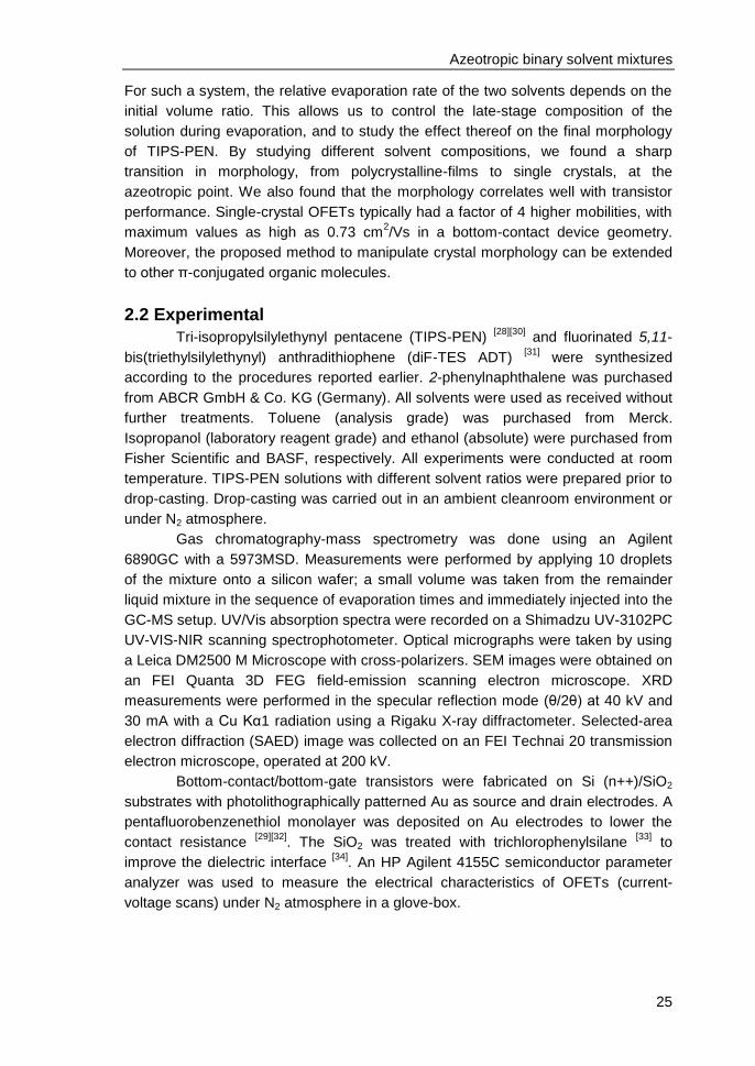
Azeotropic binary solvent mixtures
25
For such a system, the relative evaporation rate of the two solvents depends on the
initial volume ratio. This allows us to control the late-stage composition of the
solution during evaporation, and to study the effect thereof on the final morphology
of TIPS-PEN. By studying different solvent compositions, we found a sharp
transition in morphology, from polycrystalline-films to single crystals, at the
azeotropic point. We also found that the morphology correlates well with transistor
performance. Single-crystal OFETs typically had a factor of 4 higher mobilities, with
maximum values as high as 0.73 cm2/Vs in a bottom-contact device geometry.
Moreover, the proposed method to manipulate crystal morphology can be extended
to other π-conjugated organic molecules.
2.2 Experimental
Tri-isopropylsilylethynyl pentacene (TIPS-PEN) [28][30]
and fluorinated 5,11-
bis(triethylsilylethynyl) anthradithiophene (diF-TES ADT) [31]
were synthesized
according to the procedures reported earlier. 2-phenylnaphthalene was purchased
from ABCR GmbH & Co. KG (Germany). All solvents were used as received without
further treatments. Toluene (analysis grade) was purchased from Merck.
Isopropanol (laboratory reagent grade) and ethanol (absolute) were purchased from
Fisher Scientific and BASF, respectively. All experiments were conducted at room
temperature. TIPS-PEN solutions with different solvent ratios were prepared prior to
drop-casting. Drop-casting was carried out in an ambient cleanroom environment or
under N2 atmosphere.
Gas chromatography-mass spectrometry was done using an Agilent
6890GC with a 5973MSD. Measurements were performed by applying 10 droplets
of the mixture onto a silicon wafer; a small volume was taken from the remainder
liquid mixture in the sequence of evaporation times and immediately injected into the
GC-MS setup. UV/Vis absorption spectra were recorded on a Shimadzu UV-3102PC
UV-VIS-NIR scanning spectrophotometer. Optical micrographs were taken by using
a Leica DM2500 M Microscope with cross-polarizers. SEM images were obtained on
an FEI Quanta 3D FEG field-emission scanning electron microscope. XRD
measurements were performed in the specular reflection mode (θ/2θ) at 40 kV and
30 mA with a Cu Kα1 radiation using a Rigaku X-ray diffractometer. Selected-area
electron diffraction (SAED) image was collected on an FEI Technai 20 transmission
electron microscope, operated at 200 kV.
Bottom-contact/bottom-gate transistors were fabricated on Si (n++)/SiO2
substrates with photolithographically patterned Au as source and drain electrodes. A
pentafluorobenzenethiol monolayer was deposited on Au electrodes to lower the
contact resistance [29][32]
. The SiO2 was treated with trichlorophenylsilane [33]
to
improve the dielectric interface [34]
. An HP Agilent 4155C semiconductor parameter
analyzer was used to measure the electrical characteristics of OFETs (current-
voltage scans) under N2 atmosphere in a glove-box.
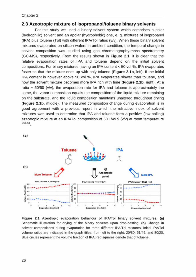
Chapter 2
26
2.3 Azeotropic mixture of isopropanol/toluene binary solvents
For this study we used a binary solvent system which comprises a polar
(hydrophilic) solvent and an apolar (hydrophobic) one, e. g. mixtures of isopropanol
(IPA) plus toluene (Tol) with different IPA/Tol ratios (v/v). When these binary solvent
mixtures evaporated on silicon wafers in ambient condition, the temporal change in
solvent composition was studied using gas chromatography-mass spectrometry
(GC-MS), respectively. From the results shown in Figure 2.1, it is clear that the
relative evaporation rates of IPA and toluene depend on the initial solvent
compositions. For binary mixtures having an IPA content < 50 vol %, IPA evaporates
faster so that the mixture ends up with only toluene (Figure 2.1b, left). If the initial
IPA content is however above 50 vol %, IPA evaporates slower than toluene, and
now the solvent mixture becomes more IPA rich with time (Figure 2.1b, right). At a
ratio ~ 50/50 (v/v), the evaporation rate for IPA and toluene is approximately the
same, the vapor composition equals the composition of the liquid mixture remaining
on the substrate, and the liquid composition maintains unaltered throughout drying
(Figure 2.1b, middle). The measured composition change during evaporation is in
good agreement with a previous report in which the refractive index of solvent
mixtures was used to determine that IPA and toluene form a positive (low-boiling)
azeotropic mixture at an IPA/Tol composition of 50.1/49.9 (v/v) at room temperature [25][26]
.
Figure 2.1 Azeotropic evaporation behaviour of IPA/Tol binary solvent mixtures. (a)
Schematic illustration for drying of the binary solvents upon drop-casting. (b) Change in
solvent compositions during evaporation for three different IPA/Tol mixtures. Initial IPA/Tol
volume ratios are indicated in the graph titles, from left to the right: 20/80; 51/49; and 80/20.
Blue circles represent the volume fraction of IPA; red squares denote that of toluene.
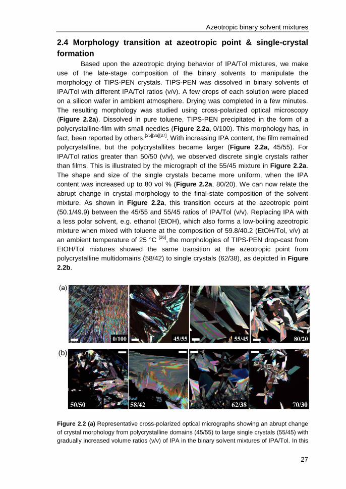
Azeotropic binary solvent mixtures
27
2.4 Morphology transition at azeotropic point & single-crystal
formation
Based upon the azeotropic drying behavior of IPA/Tol mixtures, we make
use of the late-stage composition of the binary solvents to manipulate the
morphology of TIPS-PEN crystals. TIPS-PEN was dissolved in binary solvents of
IPA/Tol with different IPA/Tol ratios (v/v). A few drops of each solution were placed
on a silicon wafer in ambient atmosphere. Drying was completed in a few minutes.
The resulting morphology was studied using cross-polarized optical microscopy
(Figure 2.2a). Dissolved in pure toluene, TIPS-PEN precipitated in the form of a
polycrystalline-film with small needles (Figure 2.2a, 0/100). This morphology has, in
fact, been reported by others [35][36][37]
. With increasing IPA content, the film remained
polycrystalline, but the polycrystallites became larger (Figure 2.2a, 45/55). For
IPA/Tol ratios greater than 50/50 (v/v), we observed discrete single crystals rather
than films. This is illustrated by the micrograph of the 55/45 mixture in Figure 2.2a.
The shape and size of the single crystals became more uniform, when the IPA
content was increased up to 80 vol % (Figure 2.2a, 80/20). We can now relate the
abrupt change in crystal morphology to the final-state composition of the solvent
mixture. As shown in Figure 2.2a, this transition occurs at the azeotropic point
(50.1/49.9) between the 45/55 and 55/45 ratios of IPA/Tol (v/v). Replacing IPA with
a less polar solvent, e.g. ethanol (EtOH), which also forms a low-boiling azeotropic
mixture when mixed with toluene at the composition of 59.8/40.2 (EtOH/Tol, v/v) at
an ambient temperature of 25 °C [26]
, the morphologies of TIPS-PEN drop-cast from
EtOH/Tol mixtures showed the same transition at the azeotropic point from
polycrystalline multidomains (58/42) to single crystals (62/38), as depicted in Figure
2.2b.
Figure 2.2 (a) Representative cross-polarized optical micrographs showing an abrupt change
of crystal morphology from polycrystalline domains (45/55) to large single crystals (55/45) with
gradually increased volume ratios (v/v) of IPA in the binary solvent mixtures of IPA/Tol. In this
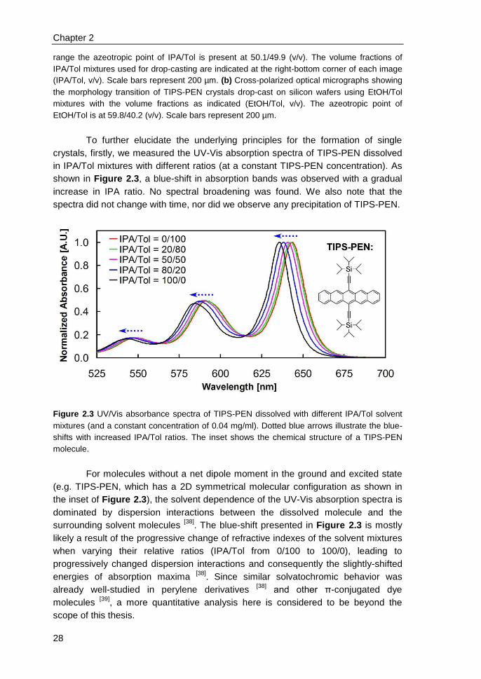
Chapter 2
28
range the azeotropic point of IPA/Tol is present at 50.1/49.9 (v/v). The volume fractions of
IPA/Tol mixtures used for drop-casting are indicated at the right-bottom corner of each image
(IPA/Tol, v/v). Scale bars represent 200 µm. (b) Cross-polarized optical micrographs showing
the morphology transition of TIPS-PEN crystals drop-cast on silicon wafers using EtOH/Tol
mixtures with the volume fractions as indicated (EtOH/Tol, v/v). The azeotropic point of
EtOH/Tol is at 59.8/40.2 (v/v). Scale bars represent 200 µm.
To further elucidate the underlying principles for the formation of single
crystals, firstly, we measured the UV-Vis absorption spectra of TIPS-PEN dissolved
in IPA/Tol mixtures with different ratios (at a constant TIPS-PEN concentration). As
shown in Figure 2.3, a blue-shift in absorption bands was observed with a gradual
increase in IPA ratio. No spectral broadening was found. We also note that the
spectra did not change with time, nor did we observe any precipitation of TIPS-PEN.
Figure 2.3 UV/Vis absorbance spectra of TIPS-PEN dissolved with different IPA/Tol solvent
mixtures (and a constant concentration of 0.04 mg/ml). Dotted blue arrows illustrate the blue-
shifts with increased IPA/Tol ratios. The inset shows the chemical structure of a TIPS-PEN
molecule.
For molecules without a net dipole moment in the ground and excited state
(e.g. TIPS-PEN, which has a 2D symmetrical molecular configuration as shown in
the inset of Figure 2.3), the solvent dependence of the UV-Vis absorption spectra is
dominated by dispersion interactions between the dissolved molecule and the
surrounding solvent molecules [38]
. The blue-shift presented in Figure 2.3 is mostly
likely a result of the progressive change of refractive indexes of the solvent mixtures
when varying their relative ratios (IPA/Tol from 0/100 to 100/0), leading to
progressively changed dispersion interactions and consequently the slightly-shifted
energies of absorption maxima [38]
. Since similar solvatochromic behavior was
already well-studied in perylene derivatives [38]
and other π-conjugated dye
molecules [39]
, a more quantitative analysis here is considered to be beyond the
scope of this thesis.
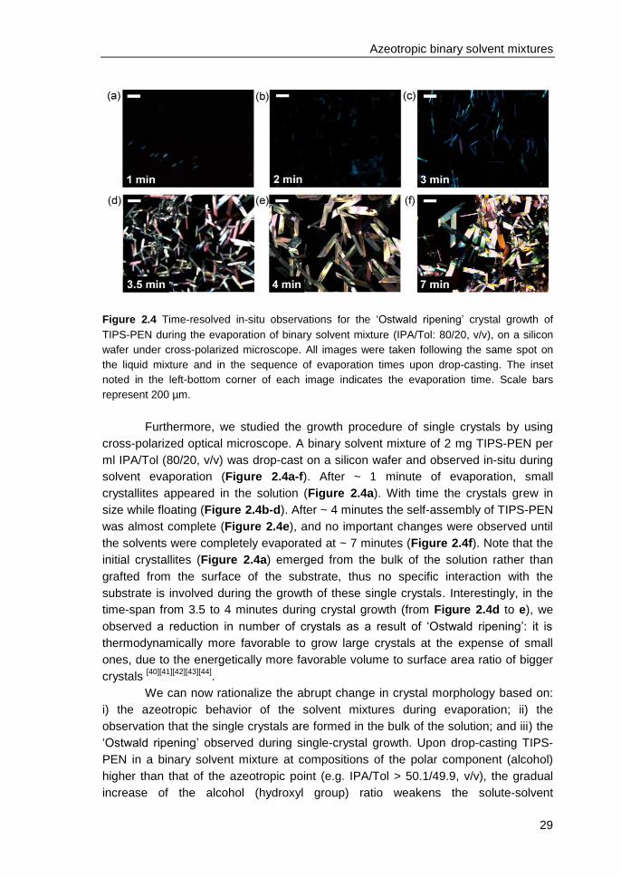
Azeotropic binary solvent mixtures
29
Figure 2.4 Time-resolved in-situ observations for the ‘Ostwald ripening’ crystal growth of
TIPS-PEN during the evaporation of binary solvent mixture (IPA/Tol: 80/20, v/v), on a silicon
wafer under cross-polarized microscope. All images were taken following the same spot on
the liquid mixture and in the sequence of evaporation times upon drop-casting. The inset
noted in the left-bottom corner of each image indicates the evaporation time. Scale bars
represent 200 µm.
Furthermore, we studied the growth procedure of single crystals by using
cross-polarized optical microscope. A binary solvent mixture of 2 mg TIPS-PEN per
ml IPA/Tol (80/20, v/v) was drop-cast on a silicon wafer and observed in-situ during
solvent evaporation (Figure 2.4a-f). After ~ 1 minute of evaporation, small
crystallites appeared in the solution (Figure 2.4a). With time the crystals grew in
size while floating (Figure 2.4b-d). After ~ 4 minutes the self-assembly of TIPS-PEN
was almost complete (Figure 2.4e), and no important changes were observed until
the solvents were completely evaporated at ~ 7 minutes (Figure 2.4f). Note that the
initial crystallites (Figure 2.4a) emerged from the bulk of the solution rather than
grafted from the surface of the substrate, thus no specific interaction with the
substrate is involved during the growth of these single crystals. Interestingly, in the
time-span from 3.5 to 4 minutes during crystal growth (from Figure 2.4d to e), we
observed a reduction in number of crystals as a result of ‘Ostwald ripening’: it is
thermodynamically more favorable to grow large crystals at the expense of small
ones, due to the energetically more favorable volume to surface area ratio of bigger
crystals [40][41][42][43][44]
.
We can now rationalize the abrupt change in crystal morphology based on:
i) the azeotropic behavior of the solvent mixtures during evaporation; ii) the
observation that the single crystals are formed in the bulk of the solution; and iii) the
‘Ostwald ripening’ observed during single-crystal growth. Upon drop-casting TIPS-
PEN in a binary solvent mixture at compositions of the polar component (alcohol)
higher than that of the azeotropic point (e.g. IPA/Tol > 50.1/49.9, v/v), the gradual
increase of the alcohol (hydroxyl group) ratio weakens the solute-solvent
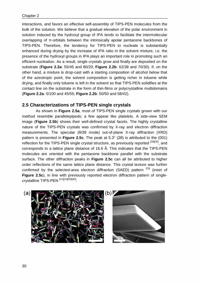
Chapter 2
30
interactions, and favors an effective self-assembly of TIPS-PEN molecules from the
bulk of the solution. We believe that a gradual elevation of the polar environment in
solution induced by the hydroxyl group of IPA tends to facilitate the intermolecular
overlapping of π-orbitals between the intrinsically apolar pentacene backbones of
TIPS-PEN. Therefore, the tendency for TIPS-PEN to nucleate is substantially
enhanced during drying by the increase of IPA ratio in the solvent mixture, i.e. the
presence of the hydroxyl groups in IPA plays an important role in promoting such an
efficient nucleation. As a result, single crystals grow and finally are deposited on the
substrate (Figure 2.2a: 55/45 and 80/20; Figure 2.2b: 62/38 and 70/30). If, on the
other hand, a mixture is drop-cast with a starting composition of alcohol below that
of the azeotropic point, the solvent composition is getting richer in toluene while
drying, and finally only toluene is left in the solvent so that TIPS-PEN solidifies at the
contact line on the substrate in the form of thin-films or polycrystalline multidomains
(Figure 2.2a: 0/100 and 45/55; Figure 2.2b: 50/50 and 58/42).
2.5 Characterizations of TIPS-PEN single crystals
As shown in Figure 2.5a, most of TIPS-PEN single crystals grown with our
method resemble parallelepipeds; a few appear like platelets. A side-view SEM
image (Figure 2.5b) shows their well-defined crystal facets. The highly crystalline
nature of the TIPS-PEN crystals was confirmed by X-ray and electron diffraction
measurements. The specular (θ/2θ mode) out-of-plane X-ray diffraction (XRD)
pattern is presented in Figure 2.5c. The peak at 5.3° (2θ) is attributed to the (001)
reflection for the TIPS-PEN single crystal structure, as previously reported [28][35]
, and
corresponds to a lattice plane distance of 16.6 Å. This indicates that the TIPS-PEN
molecules are oriented with the pentacene backbone parallel with the substrate
surface. The other diffraction peaks in Figure 2.5c can all be attributed to higher
order reflections of the same lattice plane distance. This crystal texture was further
confirmed by the selected-area electron diffraction (SAED) pattern [23]
(inset of
Figure 2.5c), in line with previously reported electron diffraction pattern of single-
crystalline TIPS-PEN [21][23][35][45]
.
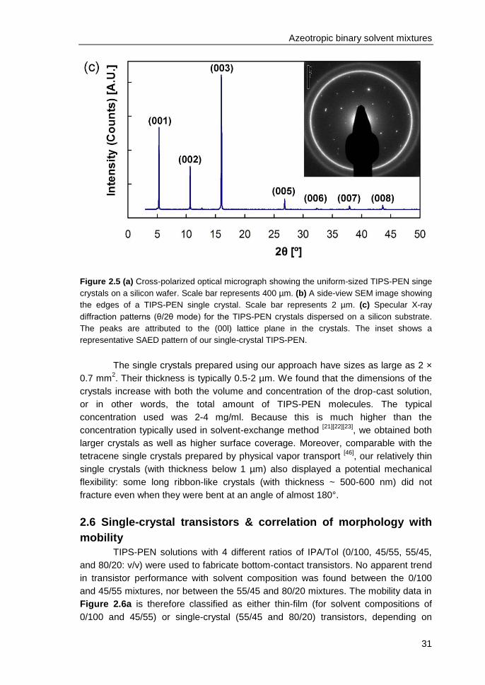
Azeotropic binary solvent mixtures
31
Figure 2.5 (a) Cross-polarized optical micrograph showing the uniform-sized TIPS-PEN singe
crystals on a silicon wafer. Scale bar represents 400 µm. (b) A side-view SEM image showing
the edges of a TIPS-PEN single crystal. Scale bar represents 2 µm. (c) Specular X-ray
diffraction patterns (θ/2θ mode) for the TIPS-PEN crystals dispersed on a silicon substrate.
The peaks are attributed to the (00l) lattice plane in the crystals. The inset shows a
representative SAED pattern of our single-crystal TIPS-PEN.
The single crystals prepared using our approach have sizes as large as 2 ×
0.7 mm2. Their thickness is typically 0.5-2 µm. We found that the dimensions of the
crystals increase with both the volume and concentration of the drop-cast solution,
or in other words, the total amount of TIPS-PEN molecules. The typical
concentration used was 2-4 mg/ml. Because this is much higher than the
concentration typically used in solvent-exchange method [21][22][23]
, we obtained both
larger crystals as well as higher surface coverage. Moreover, comparable with the
tetracene single crystals prepared by physical vapor transport [46]
, our relatively thin
single crystals (with thickness below 1 µm) also displayed a potential mechanical
flexibility: some long ribbon-like crystals (with thickness ~ 500-600 nm) did not
fracture even when they were bent at an angle of almost 180°.
2.6 Single-crystal transistors & correlation of morphology with
mobility
TIPS-PEN solutions with 4 different ratios of IPA/Tol (0/100, 45/55, 55/45,
and 80/20: v/v) were used to fabricate bottom-contact transistors. No apparent trend
in transistor performance with solvent composition was found between the 0/100
and 45/55 mixtures, nor between the 55/45 and 80/20 mixtures. The mobility data in
Figure 2.6a is therefore classified as either thin-film (for solvent compositions of
0/100 and 45/55) or single-crystal (55/45 and 80/20) transistors, depending on
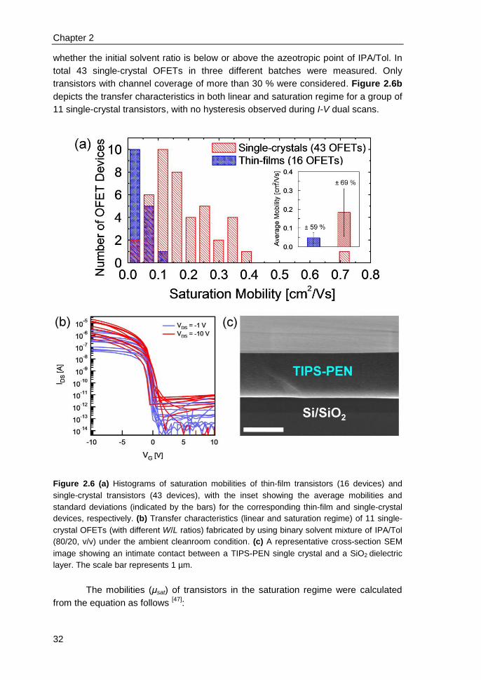
Chapter 2
32
whether the initial solvent ratio is below or above the azeotropic point of IPA/Tol. In
total 43 single-crystal OFETs in three different batches were measured. Only
transistors with channel coverage of more than 30 % were considered. Figure 2.6b
depicts the transfer characteristics in both linear and saturation regime for a group of
11 single-crystal transistors, with no hysteresis observed during I-V dual scans.
Figure 2.6 (a) Histograms of saturation mobilities of thin-film transistors (16 devices) and
single-crystal transistors (43 devices), with the inset showing the average mobilities and
standard deviations (indicated by the bars) for the corresponding thin-film and single-crystal
devices, respectively. (b) Transfer characteristics (linear and saturation regime) of 11 single-
crystal OFETs (with different W/L ratios) fabricated by using binary solvent mixture of IPA/Tol
(80/20, v/v) under the ambient cleanroom condition. (c) A representative cross-section SEM
image showing an intimate contact between a TIPS-PEN single crystal and a SiO2 dielectric
layer. The scale bar represents 1 µm.
The mobilities (μsat) of transistors in the saturation regime were calculated
from the equation as follows [47]
:
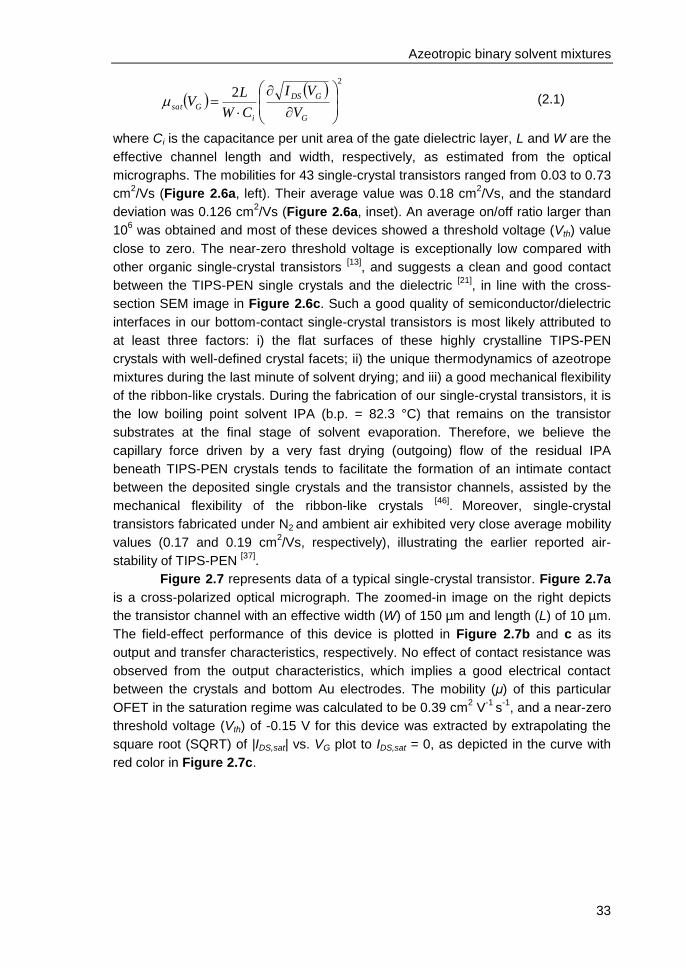
Azeotropic binary solvent mixtures
33
2
2
G
GDS
i
GsatV
VI
CW
LV (2.1)
where Ci is the capacitance per unit area of the gate dielectric layer, L and W are the
effective channel length and width, respectively, as estimated from the optical
micrographs. The mobilities for 43 single-crystal transistors ranged from 0.03 to 0.73
cm2/Vs (Figure 2.6a, left). Their average value was 0.18 cm
2/Vs, and the standard
deviation was 0.126 cm2/Vs (Figure 2.6a, inset). An average on/off ratio larger than
106 was obtained and most of these devices showed a threshold voltage (Vth) value
close to zero. The near-zero threshold voltage is exceptionally low compared with
other organic single-crystal transistors [13]
, and suggests a clean and good contact
between the TIPS-PEN single crystals and the dielectric [21]
, in line with the cross-
section SEM image in Figure 2.6c. Such a good quality of semiconductor/dielectric
interfaces in our bottom-contact single-crystal transistors is most likely attributed to
at least three factors: i) the flat surfaces of these highly crystalline TIPS-PEN
crystals with well-defined crystal facets; ii) the unique thermodynamics of azeotrope
mixtures during the last minute of solvent drying; and iii) a good mechanical flexibility
of the ribbon-like crystals. During the fabrication of our single-crystal transistors, it is
the low boiling point solvent IPA (b.p. = 82.3 °C) that remains on the transistor
substrates at the final stage of solvent evaporation. Therefore, we believe the
capillary force driven by a very fast drying (outgoing) flow of the residual IPA
beneath TIPS-PEN crystals tends to facilitate the formation of an intimate contact
between the deposited single crystals and the transistor channels, assisted by the
mechanical flexibility of the ribbon-like crystals [46]
.
Moreover, single-crystal
transistors fabricated under N2 and ambient air exhibited very close average mobility
values (0.17 and 0.19 cm2/Vs, respectively), illustrating the earlier reported air-
stability of TIPS-PEN [37]
.
Figure 2.7 represents data of a typical single-crystal transistor. Figure 2.7a
is a cross-polarized optical micrograph. The zoomed-in image on the right depicts
the transistor channel with an effective width (W) of 150 µm and length (L) of 10 µm.
The field-effect performance of this device is plotted in Figure 2.7b and c as its
output and transfer characteristics, respectively. No effect of contact resistance was
observed from the output characteristics, which implies a good electrical contact
between the crystals and bottom Au electrodes. The mobility (μ) of this particular
OFET in the saturation regime was calculated to be 0.39 cm2 V
-1 s
-1, and a near-zero
threshold voltage (Vth) of -0.15 V for this device was extracted by extrapolating the
square root (SQRT) of |IDS,sat| vs. VG plot to IDS,sat = 0, as depicted in the curve with
red color in Figure 2.7c.
Chapter 2
34
Figure 2.7 (a) Left: Cross-polarized optical micrograph of typical single-crystal OFETs; Right:
A magnified image showing a transistor channel with channel length of 10 µm and width of
150 µm, respectively. (b) Output characteristics and (c) transfer characteristics (VDS = -10 V)
of the device shown in (a). Curves of IDS with different colors in (b) correspond to different
gate-bias (VG): black = 0 V, red = -2.5 V, blue = -5 V, green = -7.5 V and purple = -10 V,
respectively.
The morphology of OSC is one of the dominating factors for its electronic
performance [2][9][12][35]
. We also found a clear correlation between the morphology
category (thin-films or single-crystals) and the field-effect mobility of the transistors.
The mobility of the single-crystal transistors was a factor of ~ 4 higher, which is close
to a previously reported value of ~ 4.4 [21]
. Other transistor parameters such as
threshold voltage were independent of the morphology. For both groups of devices
(thin-films and single-crystals), the range in mobility was rather broad (Figure 2.6a,
inset, approximately ± 60 % and ± 70 %, respectively). We note that this relatively
large spread is in fact expected, since the crystal orientation with respect to the
transistor channel direction is not controlled and the charge transport in this material
is dependent on the crystallographic direction [48]
. However, the spread can not only
be attributed to the intrinsic anisotropy of charge-transport in single crystals. Also
variations of the crystal quality and/or the contact of the crystals with Au bottom
electrodes can be of importance, as suggested elsewhere [49]
.
2.7 Applicability to other π-conjugated molecules
In light of the single crystal formation of TIPS-PEN, we chose two other π-
conjugated molecules and studied their crystal formation by using azeotropic binary
solvent mixtures. A soluble acene-based OSC, fluorinated 5,11-
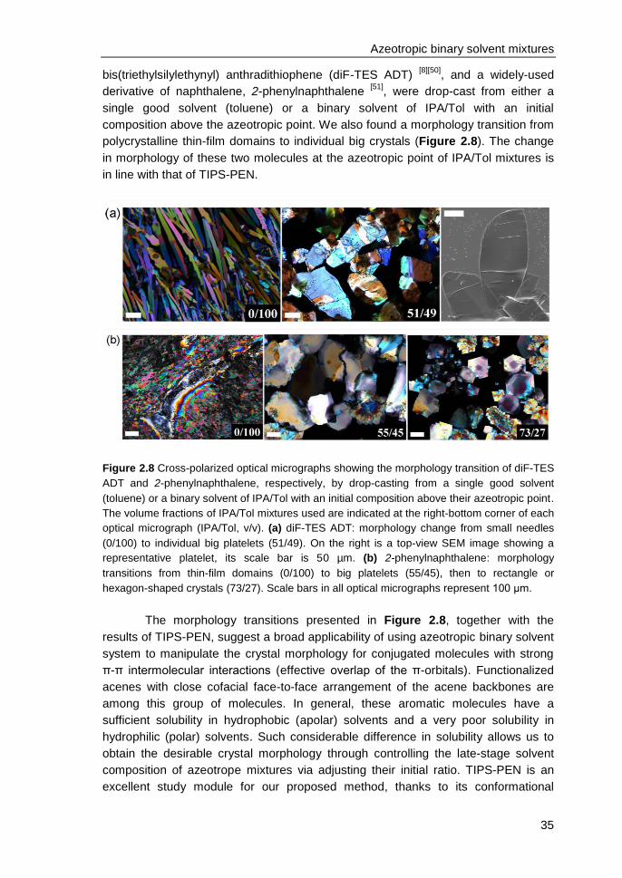
Azeotropic binary solvent mixtures
35
bis(triethylsilylethynyl) anthradithiophene (diF-TES ADT) [8][50]
, and a widely-used
derivative of naphthalene, 2-phenylnaphthalene [51]
, were drop-cast from either a
single good solvent (toluene) or a binary solvent of IPA/Tol with an initial
composition above the azeotropic point. We also found a morphology transition from
polycrystalline thin-film domains to individual big crystals (Figure 2.8). The change
in morphology of these two molecules at the azeotropic point of IPA/Tol mixtures is
in line with that of TIPS-PEN.
Figure 2.8 Cross-polarized optical micrographs showing the morphology transition of diF-TES
ADT and 2-phenylnaphthalene, respectively, by drop-casting from a single good solvent
(toluene) or a binary solvent of IPA/Tol with an initial composition above their azeotropic point.
The volume fractions of IPA/Tol mixtures used are indicated at the right-bottom corner of each
optical micrograph (IPA/Tol, v/v). (a) diF-TES ADT: morphology change from small needles
(0/100) to individual big platelets (51/49). On the right is a top-view SEM image showing a
representative platelet, its scale bar is 50 µm. (b) 2-phenylnaphthalene: morphology
transitions from thin-film domains (0/100) to big platelets (55/45), then to rectangle or
hexagon-shaped crystals (73/27). Scale bars in all optical micrographs represent 100 μm.
The morphology transitions presented in Figure 2.8, together with the
results of TIPS-PEN, suggest a broad applicability of using azeotropic binary solvent
system to manipulate the crystal morphology for conjugated molecules with strong
π-π intermolecular interactions (effective overlap of the π-orbitals). Functionalized
acenes with close cofacial face-to-face arrangement of the acene backbones are
among this group of molecules. In general, these aromatic molecules have a
sufficient solubility in hydrophobic (apolar) solvents and a very poor solubility in
hydrophilic (polar) solvents. Such considerable difference in solubility allows us to
obtain the desirable crystal morphology through controlling the late-stage solvent
composition of azeotrope mixtures via adjusting their initial ratio. TIPS-PEN is an
excellent study module for our proposed method, thanks to its conformational

Chapter 2
36
flexibility of the triisopropylsilyl side group which gives it sufficient solubility in apolar
solvents, and an increased density of its bulky groups which enables the tight
packing of the pentacene backbones to maximize their π-π interactions [21]
.
2.8 Conclusions
In conclusion, this study describes a new approach to form single crystals of
π-π stacked organic molecules by using azeotropic binary solvent mixtures. Large
crystals (length and width of up to 2 millimeters and 700 µm, respectively) of tri-
isopropylsilylethynyl pentacene with predominately parallelepiped shape are facilely
self-assembled in a well-controlled manner. Based on the concept of azeotropism
and the different solubility of TIPS-PEN in polar or apolar solvents, the size and
shape of the crystals can be manipulated from small needles to large
parallelepipeds, via adjusting the initial ratio (v/v) of the two components in our
binary solvent system with respect to their azeotropic point. We explain the
formation mechanism of large single crystals: during the evaporation of azeotrope
mixtures, the change in solvent composition promotes an efficient nucleation of
TIPS-PEN, and facilitates a fast crystallization and the ‘Ostwald ripening’ thereof.
Meanwhile, a broader applicability of our method to other π-conjugated organic
molecules is demonstrated. When used as active layer in bottom-contact field-effect
transistors, the TIPS-PEN single crystals exhibit an enhanced charge transport
properties compared to transistors with polycrystalline-films. Additionally, a higher
efficiency for the fabrication of single-crystal transistors, a better crystal coverage on
device substrates, and an improved semiconductor/dielectric interface are obtained.
The promising technological applications of organic semiconductors will
benefit from the development of efficient, inexpensive and easily controlled
deposition methods. Direct deposition of organic single crystals from solution-phase
offers an elegant and effective route. The new method described here provides a
general and rational approach to the formation of large single crystals of π-
conjugated organic molecules from solution. Its broad applicability appears to be of
interest for certain exploratory research and potential applications in materials
science, for which simplicity, rationality, and processing efficiency are the main
advantages.
2.9 References
[1] N. Stingelin-Stutzmann, Nat. Mater. 2008, 7, 171–172. [2] J.A. Lim, H.S. Lee, W.H. Lee, K. Cho, Adv. Funct. Mater. 2009, 19, 1515–
1525. [3] D. Braga, G. Horowitz, Adv. Mater. 2009, 21, 1473–1486. [4] S. Liu, W.M. Wang, A.L. Briseno, S.C.B. Mannsfeld, Z. Bao, Adv. Mater.
2009, 21, 1217–1232. [5] H.E.A. Huitema, G.H. Gelinck, J.B.P.H. van der Putten, K.E. Kuijk, C.M. Hart,
E. Cantatore, P.T. Herwig, A.J.J.M. van Breemen, D.M. de Leeuw, Nature 2001, 414, 599.
Azeotropic binary solvent mixtures
37
[6] E. Cantatore, T.C.T. Geuns, G.H. Gelinck, E. van Veenendaal, A.F.A. Gruijthuijsen, L. Schrijnemakers, S. Drews, D.M. de Leeuw, IEEE J. Solid-State Circuits 2007, 42, 84–92.
[7] C.S. Kim, S. Lee, E.D. Gomez, J.E. Anthony, Y.-L. Loo, Appl. Phys. Lett. 2008, 93, 103302.
[8] D.J. Gundlach, J.E. Royer, S.K. Park, S. Subramanian, O.D. Jurchescu, B.H. Hamadani, A.J. Moad, R.J. Kline, L.C. Teague, O. Kirillov, C.A. Richter, J.G. Kushmerick, L.J. Richter, S.R. Parkin, T.N. Jackson, J.E. Anthony, Nat. Mater. 2008, 7, 216–221.
[9] S.K. Park, T.N. Jackson, J.E. Anthony, D.A. Mourey, Appl. Phys. Lett. 2007, 91, 063514.
[10] N. Liu, Y. Zhou, L. Wang, J. Peng, J. Wang, J. Pei, Y. Cao, Langmuir 2009, 25, 665–671.
[11] J.A. Lim, W.H. Lee, H.S. Lee, J.H. Lee, Y.D. Park, K. Cho, Adv. Funct. Mater. 2008, 18, 229–234.
[12] I. Mcculloch, Nat. Mater. 2005, 4, 583–584. [13] Q. Tang, L. Jiang, Y. Tong, H. Li, Y. Liu, Z. Wang, W. Hu, Y. Liu, D. Zhu,
Adv. Mater. 2008, 20, 2947–2951. [14] A.L. Briseno, S.C.B. Mannsfeld, S.A. Jenekhe, Z. Bao, Y. Xia, Mater. Today
2008, 11, 38–47. [15] C. Reese, Z. Bao, Mater. Today 2007, 10, 20–27. [16] A. Molinari, I. Gutierrez, I.N. Hulea, S. Russo, A.F. Morpurgo, Appl. Phys.
Lett. 2007, 90, 212103. [17] E. Menard, A. Marchenko, V. Podzorov, M.E. Gershenson, D. Fichou, J.A.
Rogers, Adv. Mater. 2006, 18, 1552–1556. [18] Y. Sun, L. Tan, S. Jiang, H. Qian, Z. Wang, D. Yan, C. Di, Y. Wang, W. Wu,
G. Yu, S. Yan, C. Wang, W. Hu, Y. Liu, D. Zhu, J. Am. Chem. Soc. 2007, 129, 1882–1883.
[19] V.Y. Butko, X. Chi, D.V. Lang, A.P. Ramirez, Appl. Phys. Lett. 2003, 83, 4773–4775.
[20] A.S. Molinari, H. Alves, Z. Chen, A. Facchetti, A.F. Morpurgo, J. Am. Chem. Soc. 2009, 131, 2462–2463.
[21] D.H. Kim, D.Y. Lee, H.S. Lee, W.H. Lee, Y.H. Kim, J.I. Han, K. Cho, Adv. Mater. 2007, 19, 678–682.
[22] K. Balakrishnan, A. Datar, R. Oitker, H. Chen, J. Zuo, L. Zang, J. Am. Chem. Soc. 2005, 127, 10496–10497.
[23] S.J. Kang, I. Bae, Y.J. Park, T.H. Park, J. Sung, S.C. Yoon, K.H. Kim, D.H. Choi, C. Park, Adv. Funct. Mater. 2009, 19, 1609–1616.
[24] S.J. Kang, Y.J. Park, I. Bae, K.J. Kim, H. Kim, S. Bauer, E.L. Thomas, C. Park, Adv. Funct. Mater. 2009, 19, 2812–2818.
[25] P.W. Atkins, Physical Chemistry, 5th Ed., Oxford University Press, UK 1994, p. 245.
[26] E. Robinson, W.A. Wright, G.W. Bennett, J. Phys. Chem. 1932, 36, 658–663. [27] J. Gmehling, J. Menke, J. Krafczyk, Azeotropic Data, 2nd Ed., Vol. 1, Wiley-
VCH, Weinheim, Germany 2004. [28] J.E. Anthony, J.S. Brooks, D.L. Eaton, S.R. Parkin, J. Am. Chem. Soc. 2001,
123, 9482–9483. [29] M.M. Payne, S.R. Parkin, J.E. Anthony, C.C. Kuo, T.N. Jackson, J. Am.
Chem. Soc. 2005, 127, 4986–4987. [30] J.E. Anthony, D.L. Eaton, S.R. Parkin, Org. Lett. 2002, 4, 15–18. [31] S. Subramanian, S.K. Park, S.R. Parkin, V. Podzorov, T.N. Jackson, J.E.
Anthony, J. Am. Chem. Soc. 2008, 130, 2706–2707.
Chapter 2
38
[32] D.J. Gundlach, L.L. Jia, T.N. Jackson, IEEE Electron Device Lett. 2001, 22, 571–573.
[33] D. Janssen, R. De Palma, S. Verlaak, P. Heremans, W. Dehaen, Thin Solid Films 2006, 515, 1433–1438.
[34] D. Kumaki, M. Yahiro, Y. Inoue, S. Tokito, Appl. Phys. Lett. 2007, 90, 133511.
[35] J.H. Chen, D.C. Martin, J.E. Anthony, J. Mater. Res. 2007, 22, 1701–1709. [36] J.H. Chen, S. Subramanian, S.R. Parkin, M. Siegler, K. Gallup, C. Haughn,
D.C. Martin, J.E. Anthony, J. Mater. Chem. 2008, 18, 1961–1969. [37] S.K. Park, D.A. Mourey, J.-I. Han, J.E. Anthony, T.N. Jackson, Org. Electron.
2009, 10, 486–490. [38] E.E. Neuteboom, S.C.J. Meskers, E.H.A. Beckers, S. Chopin, R.A.J.
Janssen, J. Phys. Chem. A 2006, 110, 12363–12371. [39] M. Pope, C.E. Swenberg, Electronic Processes in Organic Crystals and
Polymers, 2nd Ed., Oxford University Press, New York, USA 1999. [40] J.D. Ng, B. Lorber, J. Witz, A. Theobald-Dietrich, D. Kern, R. Giege, J. Cryst.
Growth 1996, 168, 50–62. [41] R. Boistelle, J.P. Astier, J. Cryst. Growth 1988, 90, 14–30. [42] A. Kabalnov, J. Dispersion Sci. Technol. 2001, 22, 1–12. [43] T. Kraska, J. Phys. Chem. B 2008, 112, 12408–12413. [44] P. Taylor, Adv. Colloid Interface Sci. 2003, 106, 261–285. [45] J.H. Chen, J.E. Anthony, D.C. Martin, J. Phys. Chem. B 2006, 110, 16397–
16403. [46] R.W.I. de Boer, T.M. Klapwijk, A.F. Morpurgo, Appl. Phys. Lett. 2003, 83,
4345–4347. [47] G. Horowitz, Adv. Mater. 1998, 10, 365–377. [48] O. Ostroverkhova, D.G. Cooke, F.A. Hegmann, R.R. Tykwinski, S.R. Parkin,
J.E. Anthony, Appl. Phys. Lett. 2006, 89, 192113. [49] M. Mas-Torrent, M. Durkut, P. Hadley, X. Ribas, C. Rovira, J. Am. Chem.
Soc. 2004, 126, 984–985. [50] O.D. Jurchescu, S. Subramanian, R.J. Kline, S.D. Hudson, J.E. Anthony,
T.N. Jackson, D.J. Gundlach, Chem. Mater. 2008, 20, 6733–6737. [51] H.E. Holloway, R.V. Nauman, J.H. Wharton, J. Phys. Chem. 1968, 72,
4474–4482.
39
CHAPTER III
3. High-performance ink-jet printed
single-droplet transistors based on a
small molecule/insulating polymer
blend
In this chapter we will present a systematic study of the influence of material
composition and ink-jet processing conditions on the charge transport in bottom-gate
field-effect transistors based on blends of 6,13-bis(triisopropyl-silylethynyl)
pentacene (TIPS-PEN) and polystyrene. After careful process optimizations of
blending ratio and printing temperature we routinely make transistors with an
average mobility of 1 cm2/Vs (maximum value 1.5 cm
2/Vs), on/off ratio exceeding
107, sharp turn-on in current (sub-threshold slopes approaching 60 mV/decade), and
decent uniformity over large area. These characteristics are superior to the TIPS-
PEN only transistors. Using channel scaling measurements and scanning Kelvin
probe microscopy, the sharp turn-on in current in the blends is attributed to a contact
resistance that originates from a thin insulating layer between the injecting contacts
and the semiconductor channel.
Published as:
X. Li, W.T.T. Smaal, C. Kjellander, B. van der Putten, K. Gualandris, E.C.P. Smits, J.
Anthony, D.J. Broer, P.W.M. Blom, J. Genoe, G. Gelinck, Org. Electron. 2011, 12,
1319–1327.
Chapter 3
40
3.1 Introduction
Mixing of two or more material components is a common industrial route to
produce materials with tailor-made properties such as improved stiffness, impact
strength, permeability, and/or electrical and optical properties. Polymer/polymer
blends are commonly used as the active layer in organic solar cells [1][2]
. Goffri et al.
made organic transistors in which the active layer was a two-component blend
based on polythiophenes and different insulating polymers [3]
. This concept has also
been applied successfully for small-molecule organic semiconductors such as 6,13-
bis(triisopropyl-silylethynyl) pentacene (TIPS-PEN), blended with insulating or other
semiconducting polymers [4][5]
. Depending on the active materials, process
conditions, and taking into account the thermodynamical driving force towards the
most energetically favorable state and that most of the parent components in the
blend are thermodynamically immiscible or partially-miscible, a vertical stratified
morphology was achieved that leads to mobilities in field-effect transistors as high as
the devices based on neat semiconductors, or even higher [5][6]
. In most previous
studies, blends were either spin-cast [7][8][9]
or drop-cast [10][11]
. High mobility (> 1
cm2/Vs) transistors were reported only in the top-gate device geometry when spin-
casting a small-molecule organic semiconductor blended with a semiconducting
polymer [7][12][13][14]
. These techniques require additional patterning steps after
deposition if the transistors were to be integrated into circuits or display backplanes.
With drop-on-demand ink-jet printing the materials can be deposited locally,
resulting in efficient material usage and a simpler process for device integration [15]
.
The challenge is to print well-defined structures from dilute inks. By blending the
molecular semiconductor with a polymer, the viscosity of the printing solution can be
varied. Blending, however, is also expected to impact the electrical performance of
the final deposited transistor. This interplay is in fact the topic of this paper.
Two different approaches of ink-jet printing small-molecule semiconductors
have been used: printing multiple droplets which coagulate into a film covering a
relatively large area on the substrate, or single-droplet printing where each droplet
forms an individual functional deposit. The former was adopted in a recent study by
Madec et al. [16]
. They ink-jet printed multiple droplets of inks containing TIPS-PEN
and an amorphous and electrically insulating polymer, polystyrene (PS), at a
blending ratio of 1/1 (w/w). By printing from a specific binary solvent mixture and/or
using a multi-layer printing method, a continuous layer with improved morphology
was achieved, and they found an increased mobility of up to 10-2
cm2/Vs (± 71 -
80 % variance) in bottom-gate/top-contact transistors. These mobilities are however
much lower than the values of 0.12 cm2/Vs reported by Lim et al.
[17] for single-
droplet printing of neat TIPS-PEN from a solvent mixture, making it thus far unclear
if blending with an insulating polymer can result in a further improvement in high-
performance ink-jet printed transistors.
In this chapter, we investigate single-droplet ink-jet printing of TIPS-PEN/PS
blends, with each printed single droplet being an individual transistor [6][18]
. This
eliminates the need for additional patterning steps. As in the previous work of Lim [17]
,
High-performance ink-jet printed blend transistors
41
we use a bottom-gate/bottom-contact device geometry. This device architecture
offers a straightforward route for downscaling of the transistor channel length to a
few micrometers. In contrast to Lim’s work, we did not rely on the unusual concentric
ring arrangement of source and drain electrodes, because that configuration does
not allow simple device integration. Here, we use conventional interdigitated comb
structure for the source and drain electrodes.
To gain insight into the charge-transport properties of our devices, we study
the differences between the transistors based on neat TIPS-PEN and TIPS-PEN/PS
blends with respect to macroscopic device operation and local charge-transport
properties, by using channel scaling studies and surface potential profilometry,
respectively, and relate them to the morphology of the devices. The fundamental
understanding of device operation obtained for our blend transistors provides
valuable guidelines to the development of next generation transistors based on
small-molecule semiconductor and insulating polymer blends.
3.2 Experimental
6,13-Bis(triisopropyl-silylethynyl)pentacene (TIPS-PEN) was synthesized
according to literature [19]
. Polystyrene (PS), Mw = 9.58 kDa (Mn = 9.32 kDa, PDI =
1.03), was purchased from Fluka. 1,2,3,4-tetrahydronaphtalene (tetralin, purchased
from Merck) was used as the solvent.
An ink-jet printing setup with a high-precision vertical translation stage and a
Microfab glass nozzle (type MJ-ATP-01-50-DLC, 50 µm orifice diameter) was used
to print inks with a constant TIPS-PEN concentration of 20 mg/ml and varied PS
concentrations according to their blending weight ratios. Each droplet with a typical
volume of 50 pL was jetted on demand and aligned to the transistor channel region
to form an individual device, on substrates that were kept at 70 or 20 ºC. All printing
experiments were performed in ambient cleanroom conditions.
Bottom-contact/bottom-gate transistors were printed on Si (n++)/SiO2
substrates with an oxide thickness of 140 nm and photolithographically patterned Au
as source and drain electrodes. A pentafluorobenzenethiol monolayer was
deposited on Au electrodes [20]
. The SiO2 was treated with trichlorophenylsilane [21][22][23]
. The transistor channel length was varied between 2 and 40 µm. Device
characteristics were measured at room temperature in inert atmosphere using an
Agilent 4155C semiconductor parameter analyser. The field-effect mobilities of our
transistors in linear (μlin) and saturation (μsat) regime were calculated from the two
equations as follows, with VDS = -1 V and -10 V, respectively [24]
:
G
SD
DSi
GlinV
I
VCW
LV
1
(3.1)
2
2
G
GSD
i
GsatV
VI
CW
LV
(3.2)
Chapter 3
42
where Ci is the capacitance per unit area of the gate dielectric layer, and L and W
are channel length and width, respectively. The threshold voltage (Vth) of our
devices is extracted by extrapolating the square root (SQRT) of |ISD,sat| vs. VG plot to
ISD,sat = 0 (as depicted in the plots in Figure 3.1a). The sub-threshold slope (SS)
value was calculated from the measured ISD values over more than two decades
above noise level, using the following equation:
2
1
21
10logSD
SD
GG
I
I
VVSS
(3.3)
Optical micrographs were taken on a Leica DM2500M Microscope with
cross-polarizers. SKPM was performed using a Veeco Dimension 3100 with a
NanoScope IVa controller operating in the lift mode. For the comparison of contact
resistance in the neat and blend transistors, a maximized scan size of 80 × 80 μm2
was used here to span over three active channels in the transistors to rule out any
local effects. To avoid any effect of morphological anisotropy due to the direction of
crystal growth from periphery towards centre of the droplets, the scanning regions of
SKPM on two groups of devices (neat vs. blend) were chosen at the same location
relative to the exact centre of the droplets, and with the same scanning direction with
respect to the orientation of interdigitated electrodes of the devices. First, the height
profile was recorded with tapping-mode atomic force microscopy (AFM). In the
second pass the tip is lifted at a fixed height of 50 nm above the surface, and a
voltage is applied to the tip, to record the local surface potentials. Several effects
can influence the accuracy of SKPM measurements, e.g. the distance between
SKPM tip and the sample surface, the geometry of the tip and cantilever, and the
relative in-plane positioning of the cantilever with respect to the interdigitated
electrodes of transistors [25][26][27]
. The accuracy of our SKPM measurements is
comparable to earlier reports on working organic transistors [25][28][29]
, with observed
voltage drop from source to drain electrodes slightly lower than the actual bias
applied (VDS). Here we tend to attribute this smaller measured potential drops to the
effect of non-local coupling between the entire cantilever/tip and the microscopic
device surface, and/or a relatively high tip-sample distance of 50 nm in our
measurements [26][27][30][31]
.
3.3 Impact of insulating polymer (PS) on transistor device
performance
Our transistors were independently processed over a period of 14 months
on substrates that were prepared under identical conditions. Over time no significant
drift in transistor parameters was observed. Representative transfer characteristics
in saturation (VDS = -10 V) for neat TIPS-PEN transistors printed at 70 °C are shown
in Figure 3.1a (open circles in blue). Non-ideal sub-threshold behavior was
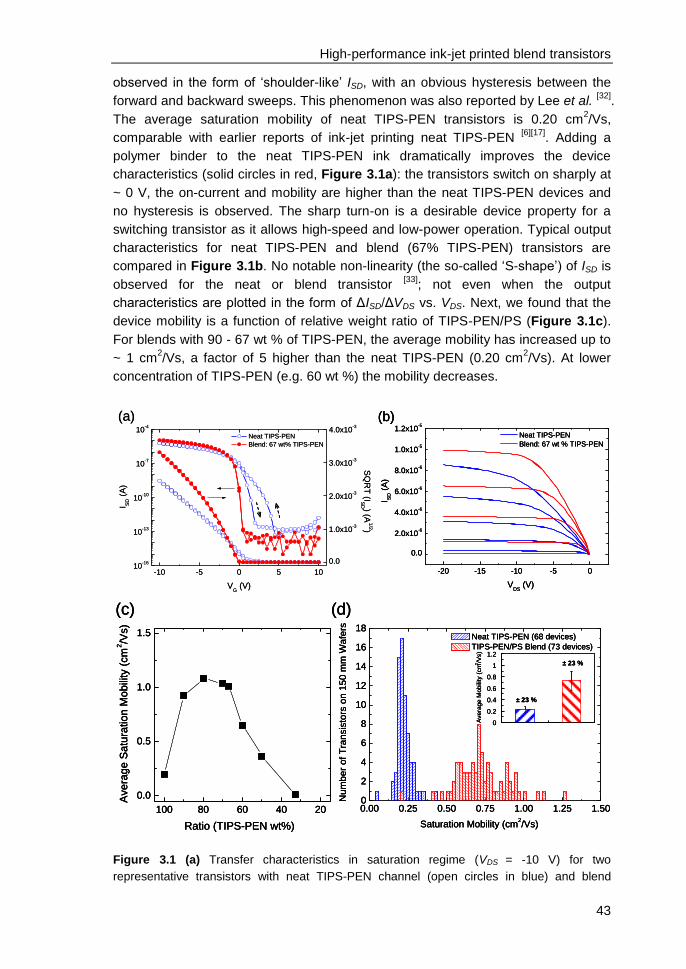
High-performance ink-jet printed blend transistors
43
observed in the form of ‘shoulder-like’ ISD, with an obvious hysteresis between the
forward and backward sweeps. This phenomenon was also reported by Lee et al. [32]
.
The average saturation mobility of neat TIPS-PEN transistors is 0.20 cm2/Vs,
comparable with earlier reports of ink-jet printing neat TIPS-PEN [6][17]
. Adding a
polymer binder to the neat TIPS-PEN ink dramatically improves the device
characteristics (solid circles in red, Figure 3.1a): the transistors switch on sharply at
~ 0 V, the on-current and mobility are higher than the neat TIPS-PEN devices and
no hysteresis is observed. The sharp turn-on is a desirable device property for a
switching transistor as it allows high-speed and low-power operation. Typical output
characteristics for neat TIPS-PEN and blend (67% TIPS-PEN) transistors are
compared in Figure 3.1b. No notable non-linearity (the so-called ‘S-shape’) of ISD is
observed for the neat or blend transistor [33]
; not even when the output
characteristics are plotted in the form of ΔISD/ΔVDS vs. VDS. Next, we found that the
device mobility is a function of relative weight ratio of TIPS-PEN/PS (Figure 3.1c).
For blends with 90 - 67 wt % of TIPS-PEN, the average mobility has increased up to
~ 1 cm2/Vs, a factor of 5 higher than the neat TIPS-PEN (0.20 cm
2/Vs). At lower
concentration of TIPS-PEN (e.g. 60 wt %) the mobility decreases.
-10 -5 0 5 1010
-16
10-13
10-10
10-7
10-4
Neat TIPS-PEN
Blend: 67 wt% TIPS-PEN
I SD (
A)
VG (V)
0.0
1.0x10⁻³
2.0x10⁻³
3.0x10⁻³
4.0x10⁻³
SQ
RT
(IS
D ) (A1
/2)
(a)
-20 -15 -10 -5 0
0.0
2.0x10⁻⁶
4.0x10⁻⁶
6.0x10⁻⁶
8.0x10⁻⁶
1.0x10⁻⁵
1.2x10⁻⁵
I SD (
A)
VDS
(V)
Neat TIPS-PEN
Blend: 67 wt % TIPS-PEN
(b)
-10 -5 0 5 1010
-16
10-13
10-10
10-7
10-4
Neat TIPS-PEN
Blend: 67 wt% TIPS-PEN
I SD (
A)
VG (V)
0.0
1.0x10⁻³
2.0x10⁻³
3.0x10⁻³
4.0x10⁻³
SQ
RT
(IS
D ) (A1
/2)
(a)
-20 -15 -10 -5 0
0.0
2.0x10⁻⁶
4.0x10⁻⁶
6.0x10⁻⁶
8.0x10⁻⁶
1.0x10⁻⁵
1.2x10⁻⁵
I SD (
A)
VDS
(V)
Neat TIPS-PEN
Blend: 67 wt % TIPS-PEN
(b)
-20 -15 -10 -5 0
0.0
2.0x10⁻⁶
4.0x10⁻⁶
6.0x10⁻⁶
8.0x10⁻⁶
1.0x10⁻⁵
1.2x10⁻⁵
I SD (
A)
VDS
(V)
Neat TIPS-PEN
Blend: 67 wt % TIPS-PEN
(b)
100 80 60 40 20
0.0
0.5
1.0
1.5
Ave
rag
e S
atu
ratio
n M
ob
ility
(cm
2/V
s)
Ratio (TIPS-PEN wt%)
(c)
0.00 0.25 0.50 0.75 1.00 1.25 1.500
2
4
6
8
10
12
14
16
18
Nu
mb
er
of
Tra
nsis
tors
on
15
0 m
m W
afe
rs
Saturation Mobility (cm2/Vs)
Neat TIPS-PEN (68 devices)
TIPS-PEN/PS Blend (73 devices)
(d)
0
0.2
0.4
0.6
0.8
1
1.2
Pure TIPS-PEN
(68 devices)
TIPS-PEN/PS
Blend (73 devices)
Avera
ge M
obili
ty (
cm
2/V
s)
± 23 %
± 23 %
100 80 60 40 20
0.0
0.5
1.0
1.5
Ave
rag
e S
atu
ratio
n M
ob
ility
(cm
2/V
s)
Ratio (TIPS-PEN wt%)
(c)
100 80 60 40 20
0.0
0.5
1.0
1.5
Ave
rag
e S
atu
ratio
n M
ob
ility
(cm
2/V
s)
Ratio (TIPS-PEN wt%)
(c)
0.00 0.25 0.50 0.75 1.00 1.25 1.500
2
4
6
8
10
12
14
16
18
Nu
mb
er
of
Tra
nsis
tors
on
15
0 m
m W
afe
rs
Saturation Mobility (cm2/Vs)
Neat TIPS-PEN (68 devices)
TIPS-PEN/PS Blend (73 devices)
(d)
0
0.2
0.4
0.6
0.8
1
1.2
Pure TIPS-PEN
(68 devices)
TIPS-PEN/PS
Blend (73 devices)
Avera
ge M
obili
ty (
cm
2/V
s)
± 23 %
± 23 %
Figure 3.1 (a) Transfer characteristics in saturation regime (VDS = -10 V) for two
representative transistors with neat TIPS-PEN channel (open circles in blue) and blend
Chapter 3
44
channel of 67 wt % TIPS-PEN and 33 wt % PS (solid circles in red). Channel length and width
are 10 μm and 200 μm, respectively. The two dashed arrows indicate the counter-clockwise
hysteresis for the neat device (gate swept from +10 V -10 V +10 V). The plot of the
square root (SQRT) of ISD vs. VG was used to extract mobility as well as the threshold voltage
(Vth): the blend device shows a mobility of 1.04 cm2/Vs and a near-zero Vth, while the neat
one has a mobility of 0.29 cm2/Vs and a Vth of 2.5 V. (b) Output characteristics of the same
two transistors as shown in (a). VG was varied between 0 and -10 V at a step of -2.5 V. (c)
Average saturation mobilities as a function of TIPS-PEN weight ratios in TIPS-PEN/PS blend
transistors (averaged from > 10 devices for each ratio). All devices were printed on 15 mm ×
15 mm square substrates at 70 °C. (d) Histograms of saturation mobilities for 68 neat TIPS-
PEN transistors and 73 blend (67 wt % TIPS-PEN) transistors printed on 150 mm wafers. The
inset shows their average mobility values. The relative variance (standard deviation divided by
the average value) is 23 % for neat TIPS-PEN as well as the blend devices. Transistors were
printed at 70 °C. Channel length and width are 5 μm and 1400 μm, respectively.
The average value and standard deviation of mobility (µ) in linear and
saturation regime, on-current (Ion), and on/off ratio (Ion/Ioff) for transistors (channel
length: 10 µm, on 15 mm × 15 mm square substrates) printed at 70 °C with different
blending ratios are summarized in Table 3.1. At a processing temperature of 20 °C
we obtain typically lower device performance (Table 3.2). To further study large area
uniformity, we printed 68 neat TIPS-PEN and 73 blend (67 wt % TIPS-PEN)
transistors with a channel length of 5 µm on 150 mm diameter (6-inch) wafers at
70 °C. The histograms in Figure 3.1d clearly demonstrate enhanced mobilities of
our blend transistors over the entire wafer, with the relative variance (standard
deviation divided by the average value) at the same level as the neat TIPS-PEN
devices (± 23 % in the inset of Figure 3.1d). This demonstrates the potential of our
blend inks for applications in large-area and low-cost organic electronics.
Table 3.1 Summary of transistor parameters for TIPS-PEN/PS transistors with different
blending ratios printed on 15 mm × 15 mm square substrates at 70 °C, under the same
processing conditions. Field-effect mobilities were extracted in linear (μlin) and saturation (μsat)
regime, on-current (Ion) and off-current were measured at VG = -10 V and +10V, respectively,
with VDS = -10 V. Data was obtained for > 10 transistors of each ratio.
Ratio (TIPS-PEN wt %) µlin (cm2/ Vs) µsat (cm
2/ Vs) Ion (µA) on/off ratio
100 0.23 ± 0.06 0.20 ± 0.07 4.5 ± 1.1 4.9x10⁶ ± 3.0x10
6
90 0.72 ± 0.14 0.93 ± 0.23 8.6 ± 1.7 1.2x10⁷ ± 1.0x10
7
80 0.90 ± 0.14 1.08 ± 0.16 9.4 ± 1.7 3.0x10⁷ ± 1.8x10
7
70 0.83 ± 0.22 1.04 ± 0.26 9.7 ± 2.8 2.9x10⁷ ± 1.7x10
7
67 0.85 ± 0.09 1.01 ± 0.12 10.8 ± 1.3 4.9x10⁷ ± 2.3x10
7
60 0.53 ± 0.24 0.66 ± 0.30 5.7 ± 2.5 3.8x10⁷ ± 6.6x10
7
50 0.30 ± 0.27 0.37 ± 0.33 3.6 ± 3.4 2.2x10⁷ ± 3.1x10
7
33 0.005 ± 0.003 0.01 ± 0.009 0.06 ± 0.04 2.1x10⁵ ± 1.6x10
5
Table 3.2 Summary of transistor parameters for TIPS-PEN/PS transistors with different
blending ratios printed on 15 mm × 15 mm square substrates at 20 °C, under the same
processing conditions. Field-effect mobilities were extracted in linear (μlin) and saturation (μsat)

High-performance ink-jet printed blend transistors
45
regime, on-current (Ion) was measured at VG = -10 V, with VDS = -10 V. Data was obtained for
> 10 transistors of each ratio.
Ratio (TIPS-PEN wt %) µlin (cm2/ Vs) µsat (cm
2/ Vs) Ion (µA)
100 0.17 ± 0.03 0.15 ± 0.05 4.4 ± 0.9
67 0.53 ± 0.13 0.55 ± 0.14 7.8 ± 1.7
50 0.58 ± 0.47 0.65 ± 0.51 8.3 ± 6.6
33 0.02 ± 0.02 0.04 ± 0.04 0.3 ± 0.3
The observation that the mobility is increased by the presence of an
insulator up to a critical blending ratio demonstrates that introducing an insulating
polymer does not negatively affect the charge transporting layer in the device. This
implies that in particular the composition and morphology of the first few nanometers
of our TIPS-PEN/PS blend are similar to that of neat TIPS-PEN, as charge transport
takes place at this zone in the semiconductor layer [34][35]
. Similar behavior was
recently reported for spin-cast blends of TIPS-PEN with poly(α-methylstyrene) [8][9]
,
and blends of TIPS-PEN or fluorinated 5,11-bis(triethylsilylethynyl)
anthradithiophene (diF-TES ADT) with a semiconducting polymer, polytriarylamine [7][12]
. The results were explained by the occurrence of vertical stratification upon
casting and solvent evaporation. During solvent drying TIPS-PEN is predominantly
expelled to both top and bottom interfaces of the deposited films [8][9][12]
. As long as
phase separation leads to almost pure phase of TIPS-PEN at the two interfaces, it
should be possible to realize transistors with good performance. This hypothesis can
explain why the mobility decreases at too high weight fraction of the polymer in our
blends: phase separation is incomplete and no continuous film of TIPS-PEN is
formed at the bottom interface of our devices. It can however not explain why the
maximum mobility of the blends is higher than that of the neat TIPS-PEN transistors.
At least two explanations have been proposed for the improved charge transport in
blend transistors based on small-molecule organic semiconductors with insulating
polymers. Ohe et al. suggested that the addition of polymer binder leads to a slower
solvent drying and hence to an improved film morphology with better uniformity [9]
.
Yoon et al. proposed that the polymer binder influences the film formation process of
the small-molecule organic semiconductors and acts indirectly as a purification
method, the so-called ‘zone-refinement effect’ during solidification [36]
.
TIPS-PEN wt %: (70 °C)
100 % 80 % 67 % 50 %
(a)TIPS-PEN wt %: (70 °C)
100 % 80 % 67 % 50 %
(a)
-10 -5 0 5 1010
-16
10-13
10-10
10-7
10-4
TIPS-PEN wt %
100%
80%
67%
50%
I SD (
A)
VG (V)
(b)
-10 -5 0 5 1010
-16
10-13
10-10
10-7
10-4
TIPS-PEN wt %
100%
80%
67%
50%
I SD (
A)
VG (V)
(b)
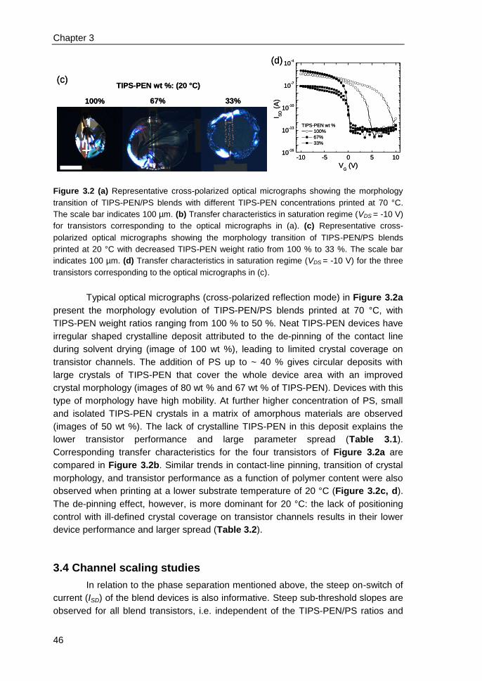
Chapter 3
46
100% 67% 33%
(c)TIPS-PEN wt %: (20 °C)
100% 67% 33%
(c)TIPS-PEN wt %: (20 °C)
-10 -5 0 5 1010
-16
10-13
10-10
10-7
10-4
TIPS-PEN wt %
100%
67%
33%
I SD (
A)
VG (V)
(d)
-10 -5 0 5 1010
-16
10-13
10-10
10-7
10-4
TIPS-PEN wt %
100%
67%
33%
I SD (
A)
VG (V)
(d)
Figure 3.2 (a) Representative cross-polarized optical micrographs showing the morphology
transition of TIPS-PEN/PS blends with different TIPS-PEN concentrations printed at 70 °C.
The scale bar indicates 100 µm. (b) Transfer characteristics in saturation regime (VDS = -10 V)
for transistors corresponding to the optical micrographs in (a). (c) Representative cross-
polarized optical micrographs showing the morphology transition of TIPS-PEN/PS blends
printed at 20 °C with decreased TIPS-PEN weight ratio from 100 % to 33 %. The scale bar
indicates 100 µm. (d) Transfer characteristics in saturation regime (VDS = -10 V) for the three
transistors corresponding to the optical micrographs in (c).
Typical optical micrographs (cross-polarized reflection mode) in Figure 3.2a
present the morphology evolution of TIPS-PEN/PS blends printed at 70 °C, with
TIPS-PEN weight ratios ranging from 100 % to 50 %. Neat TIPS-PEN devices have
irregular shaped crystalline deposit attributed to the de-pinning of the contact line
during solvent drying (image of 100 wt %), leading to limited crystal coverage on
transistor channels. The addition of PS up to ~ 40 % gives circular deposits with
large crystals of TIPS-PEN that cover the whole device area with an improved
crystal morphology (images of 80 wt % and 67 wt % of TIPS-PEN). Devices with this
type of morphology have high mobility. At further higher concentration of PS, small
and isolated TIPS-PEN crystals in a matrix of amorphous materials are observed
(images of 50 wt %). The lack of crystalline TIPS-PEN in this deposit explains the
lower transistor performance and large parameter spread (Table 3.1).
Corresponding transfer characteristics for the four transistors of Figure 3.2a are
compared in Figure 3.2b. Similar trends in contact-line pinning, transition of crystal
morphology, and transistor performance as a function of polymer content were also
observed when printing at a lower substrate temperature of 20 °C (Figure 3.2c, d).
The de-pinning effect, however, is more dominant for 20 °C: the lack of positioning
control with ill-defined crystal coverage on transistor channels results in their lower
device performance and larger spread (Table 3.2).
3.4 Channel scaling studies
In relation to the phase separation mentioned above, the steep on-switch of
current (ISD) of the blend devices is also informative. Steep sub-threshold slopes are
observed for all blend transistors, i.e. independent of the TIPS-PEN/PS ratios and
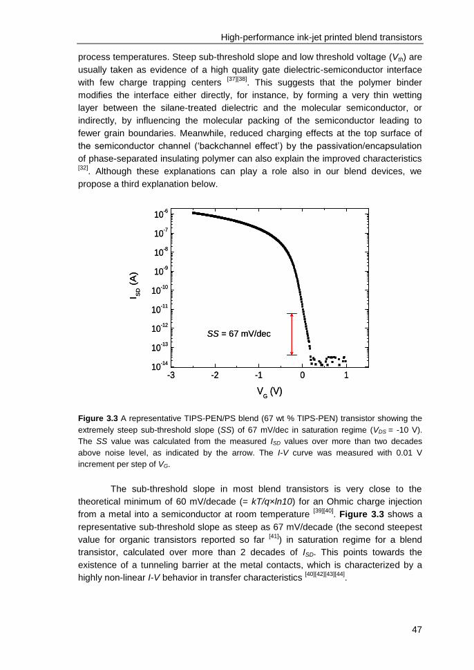
High-performance ink-jet printed blend transistors
47
process temperatures. Steep sub-threshold slope and low threshold voltage (Vth) are
usually taken as evidence of a high quality gate dielectric-semiconductor interface
with few charge trapping centers [37][38]
. This suggests that the polymer binder
modifies the interface either directly, for instance, by forming a very thin wetting
layer between the silane-treated dielectric and the molecular semiconductor, or
indirectly, by influencing the molecular packing of the semiconductor leading to
fewer grain boundaries. Meanwhile, reduced charging effects at the top surface of
the semiconductor channel (‘backchannel effect’) by the passivation/encapsulation
of phase-separated insulating polymer can also explain the improved characteristics [32]
. Although these explanations can play a role also in our blend devices, we
propose a third explanation below.
-3 -2 -1 0 110
-14
10-13
10-12
10-11
10-10
10-9
10-8
10-7
10-6
I SD (
A)
VG (V)
SS = 67 mV/dec
-3 -2 -1 0 110
-14
10-13
10-12
10-11
10-10
10-9
10-8
10-7
10-6
I SD (
A)
VG (V)
SS = 67 mV/dec
Figure 3.3 A representative TIPS-PEN/PS blend (67 wt % TIPS-PEN) transistor showing the
extremely steep sub-threshold slope (SS) of 67 mV/dec in saturation regime (VDS = -10 V).
The SS value was calculated from the measured ISD values over more than two decades
above noise level, as indicated by the arrow. The I-V curve was measured with 0.01 V
increment per step of VG.
The sub-threshold slope in most blend transistors is very close to the
theoretical minimum of 60 mV/decade (= kT/q×ln10) for an Ohmic charge injection
from a metal into a semiconductor at room temperature [39][40]
. Figure 3.3 shows a
representative sub-threshold slope as steep as 67 mV/decade (the second steepest
value for organic transistors reported so far [41]
) in saturation regime for a blend
transistor, calculated over more than 2 decades of ISD. This points towards the
existence of a tunneling barrier at the metal contacts, which is characterized by a
highly non-linear I-V behavior in transfer characteristics [40][42][43][44]
.
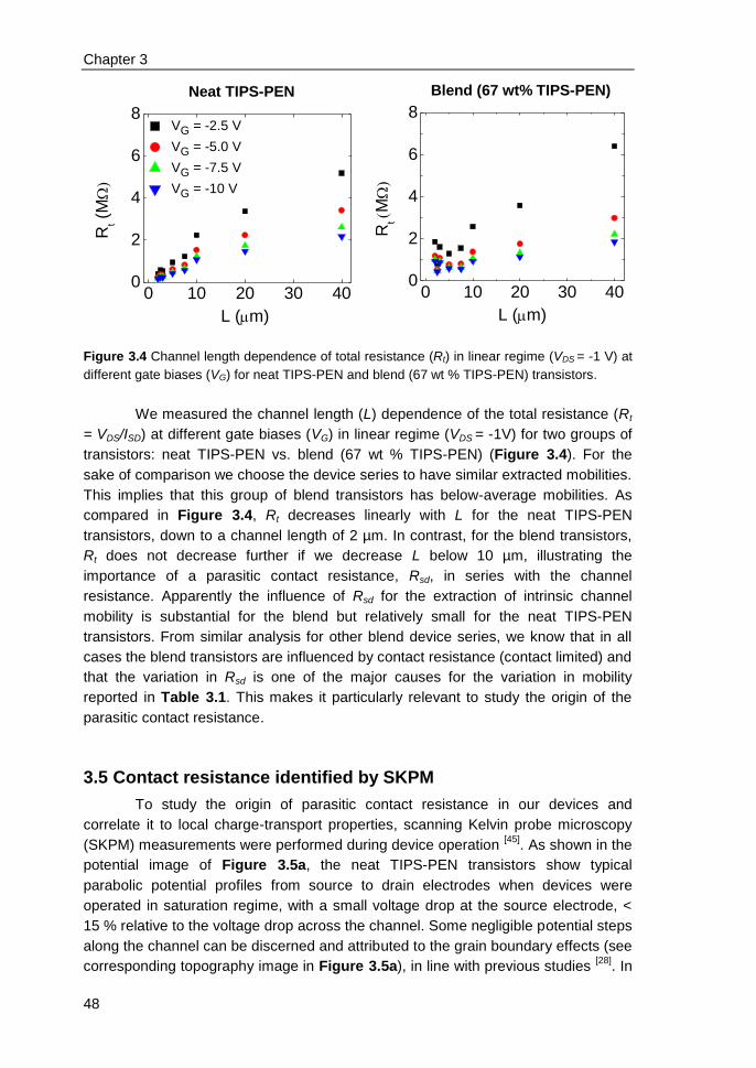
Chapter 3
48
0 10 20 30 400
2
4
6
8
Blend (67 wt% TIPS-PEN)Neat TIPS-PEN
VG = -2.5 V
VG = -5.0 V
VG = -7.5 V
VG = -10 V
R
t (M
L (m)
0 10 20 30 400
2
4
6
8
Rt
M
L (m)
-10 -8 -6 -4 -2 00.0
0.1
0.2
0.3
0.4
0.5
0.6 Corrected
i
L = 10 m
L = 20 m
L = 40 m
Mobili
ty (
cm
2/V
s)
VG (V)
-10 -8 -6 -4 -2 00.0
0.1
0.2
0.3
0.4
0.5
0.6 Corrected
i
Mobili
ty (
cm
2/V
s)
VG (V)
Figure 3.4 Channel length dependence of total resistance (Rt) in linear regime (VDS = -1 V) at
different gate biases (VG) for neat TIPS-PEN and blend (67 wt % TIPS-PEN) transistors.
We measured the channel length (L) dependence of the total resistance (Rt
= VDS/ISD) at different gate biases (VG) in linear regime (VDS = -1V) for two groups of
transistors: neat TIPS-PEN vs. blend (67 wt % TIPS-PEN) (Figure 3.4). For the
sake of comparison we choose the device series to have similar extracted mobilities.
This implies that this group of blend transistors has below-average mobilities. As
compared in Figure 3.4, Rt decreases linearly with L for the neat TIPS-PEN
transistors, down to a channel length of 2 µm. In contrast, for the blend transistors,
Rt does not decrease further if we decrease L below 10 µm, illustrating the
importance of a parasitic contact resistance, Rsd, in series with the channel
resistance. Apparently the influence of Rsd for the extraction of intrinsic channel
mobility is substantial for the blend but relatively small for the neat TIPS-PEN
transistors. From similar analysis for other blend device series, we know that in all
cases the blend transistors are influenced by contact resistance (contact limited) and
that the variation in Rsd is one of the major causes for the variation in mobility
reported in Table 3.1. This makes it particularly relevant to study the origin of the
parasitic contact resistance.
3.5 Contact resistance identified by SKPM
To study the origin of parasitic contact resistance in our devices and
correlate it to local charge-transport properties, scanning Kelvin probe microscopy
(SKPM) measurements were performed during device operation [45]
. As shown in the
potential image of Figure 3.5a, the neat TIPS-PEN transistors show typical
parabolic potential profiles from source to drain electrodes when devices were
operated in saturation regime, with a small voltage drop at the source electrode, <
15 % relative to the voltage drop across the channel. Some negligible potential steps
along the channel can be discerned and attributed to the grain boundary effects (see
corresponding topography image in Figure 3.5a), in line with previous studies [28]
. In
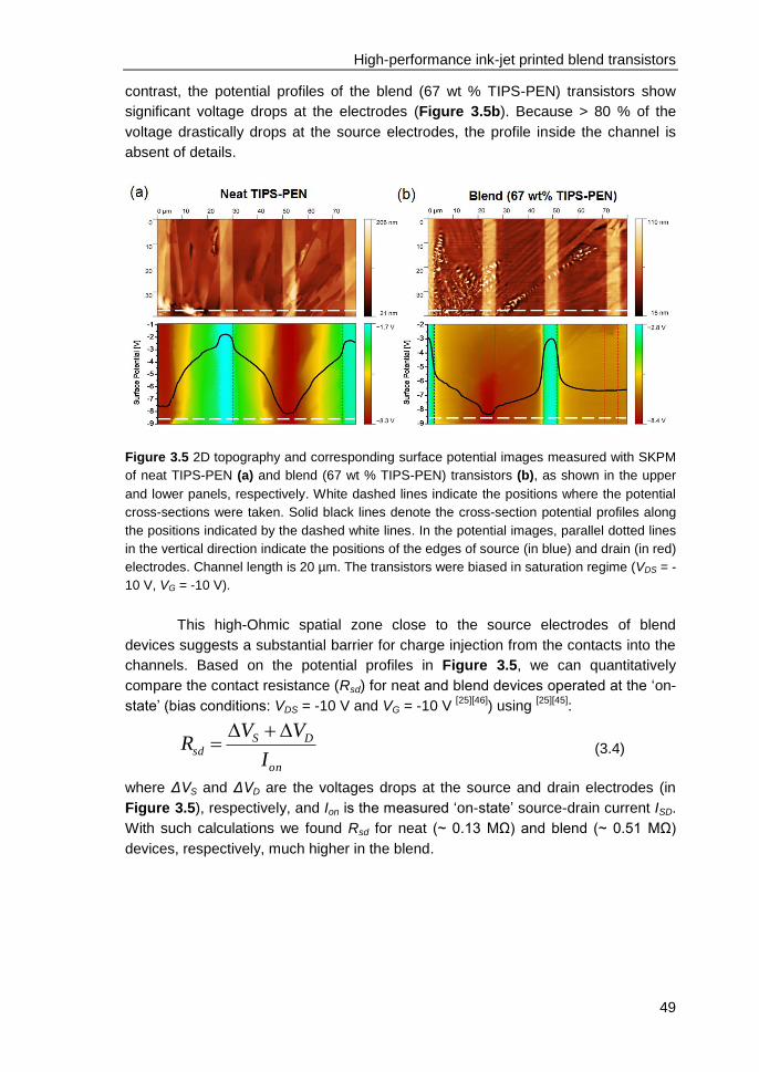
High-performance ink-jet printed blend transistors
49
contrast, the potential profiles of the blend (67 wt % TIPS-PEN) transistors show
significant voltage drops at the electrodes (Figure 3.5b). Because > 80 % of the
voltage drastically drops at the source electrodes, the profile inside the channel is
absent of details.
Figure 3.5 2D topography and corresponding surface potential images measured with SKPM
of neat TIPS-PEN (a) and blend (67 wt % TIPS-PEN) transistors (b), as shown in the upper
and lower panels, respectively. White dashed lines indicate the positions where the potential
cross-sections were taken. Solid black lines denote the cross-section potential profiles along
the positions indicated by the dashed white lines. In the potential images, parallel dotted lines
in the vertical direction indicate the positions of the edges of source (in blue) and drain (in red)
electrodes. Channel length is 20 µm. The transistors were biased in saturation regime (VDS = -
10 V, VG = -10 V).
This high-Ohmic spatial zone close to the source electrodes of blend
devices suggests a substantial barrier for charge injection from the contacts into the
channels. Based on the potential profiles in Figure 3.5, we can quantitatively
compare the contact resistance (Rsd) for neat and blend devices operated at the ‘on-
state’ (bias conditions: VDS = -10 V and VG = -10 V [25][46]
) using [25][45]
:
on
DSsd
I
VVR
(3.4)
where ΔVS and ΔVD are the voltages drops at the source and drain electrodes (in
Figure 3.5), respectively, and Ion is the measured ‘on-state’ source-drain current ISD.
With such calculations we found Rsd for neat (~ 0.13 MΩ) and blend (~ 0.51 MΩ)
devices, respectively, much higher in the blend.
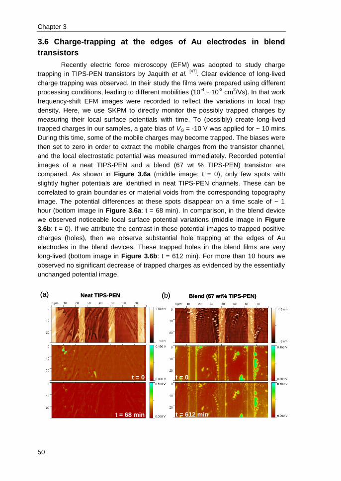
Chapter 3
50
3.6 Charge-trapping at the edges of Au electrodes in blend
transistors
Recently electric force microscopy (EFM) was adopted to study charge
trapping in TIPS-PEN transistors by Jaquith et al. [47]
. Clear evidence of long-lived
charge trapping was observed. In their study the films were prepared using different
processing conditions, leading to different mobilities (10-4
~ 10-3
cm2/Vs). In that work
frequency-shift EFM images were recorded to reflect the variations in local trap
density. Here, we use SKPM to directly monitor the possibly trapped charges by
measuring their local surface potentials with time. To (possibly) create long-lived
trapped charges in our samples, a gate bias of VG = -10 V was applied for ~ 10 mins.
During this time, some of the mobile charges may become trapped. The biases were
then set to zero in order to extract the mobile charges from the transistor channel,
and the local electrostatic potential was measured immediately. Recorded potential
images of a neat TIPS-PEN and a blend (67 wt % TIPS-PEN) transistor are
compared. As shown in Figure 3.6a (middle image: t = 0), only few spots with
slightly higher potentials are identified in neat TIPS-PEN channels. These can be
correlated to grain boundaries or material voids from the corresponding topography
image. The potential differences at these spots disappear on a time scale of ~ 1
hour (bottom image in Figure 3.6a: t = 68 min). In comparison, in the blend device
we observed noticeable local surface potential variations (middle image in Figure
3.6b: t = 0). If we attribute the contrast in these potential images to trapped positive
charges (holes), then we observe substantial hole trapping at the edges of Au
electrodes in the blend devices. These trapped holes in the blend films are very
long-lived (bottom image in Figure 3.6b: t = 612 min). For more than 10 hours we
observed no significant decrease of trapped charges as evidenced by the essentially
unchanged potential image.
Neat TIPS-PEN Blend (67 wt% TIPS-PEN)(a) (b)
t = 68 min t = 612 min
t = 0 t = 0
Neat TIPS-PEN Blend (67 wt% TIPS-PEN)(a) (b)
t = 68 min t = 612 min
t = 0 t = 0
High-performance ink-jet printed blend transistors
51
Figure 3.6 Time-dependent surface potential images and corresponding 2D topographies
recorded by SKPM, for neat TIPS-PEN (a) and blend (67 wt % TIPS-PEN) transistors (b). The
potential images in the middle row (t = 0) were measured by grounding all electrodes
immediately after a gate bias of -10 V was applied for 10 minutes. The potential images at the
bottom row were measured at t = 68 minutes and 612 minutes after three electrodes were
grounded for the neat and blend device, respectively.
It has recently been shown that insulating polymer such as poly(α-
methylstyrene) can trap charges (holes) in pentacene-based organic transistors [48]
,
and these holes remain trapped in the insulating polymer until sufficient counter
charges (electrons) can tunnel into the polymer from the channel [49]
. Based on the
clear differences of trapped charges in terms of locations, areal densities and life-
times between our neat TIPS-PEN and blend devices, we argue that the hole
trapping in our blend films is related to the local presence of insulating polymer (PS).
The potential variations in the blend films (Figure 3.6b) are explained by a lateral
phase-separation between TIPS-PEN enriched crystal grains and PS enriched
regions. In particular, our SKPM results reveal obvious hole trapping effects exactly
at the edges of the source/drain Au electrodes with no apparent correlation with its
local crystal morphology. This strongly suggests the presence of a thin film of PS (or
PS enriched phase) at the Au electrodes. Such an insulating barrier can explain the
differences in sub-threshold slope of the I-V characteristics, contact resistance
observed in channel scaling measurements, potential drops and hole trapping at the
electrodes observed by SKPM, between our neat TIPS-PEN and blend devices.
3.7 On the relation between charge-trapping, threshold voltage &
channel conductivity
If charges are trapped (de-trapped), or fixed space charges are distributed in
the transistor channel on a timescale comparable to the typical duration of the I-V
measurement, it can be observed as a hysteresis during the forward and backward
sweeps in transfer characteristics. We typically swept the voltages at a rate of 1
Volt/sec, meaning a total measurement time of ~ 1 minute.
In the case of neat TIPS-PEN transistors, non-ideal sub-threshold behavior
was observed in the form of ‘shoulder-like’ ISD, with an obvious hysteresis during
gate sweeps (Figure 3.1a). The (counter-clockwise) hysteresis was independent of
the sweep direction, i.e. it was the same when sweeping the gate biases (VG) in the
opposite direction (from -10 V +10 V -10 V). This hysteresis occurs in the
depletion regime, i.e. when the bulk of the semiconductor is (partly) depleted of
unintentional charges. We attribute it to charging effects at the top surface of the
semiconductor channel (the so-called ‘backchannel effect’), as previously reported
by Lee et al. [32]
. The transfer characteristics of our blend transistors (with different
TIPS-PEN/PS ratios) are essentially hysteresis-free, independent of the direction or
range of the gate sweeps. Apparently, the ‘backchannel effect’ is absent in these
Chapter 3
52
blend devices. This points to an additional advantage of the insulating polymer
binder. It passivates the charge transport layer.
Trapped channel charges can result in shifts of transistor threshold voltages.
Furthermore, deep and shallow trapping can also influence the charge transport
negatively. We found that in our blend devices that (i) the existence of insulating
polymer causes long-term trapping of holes, and (ii) the existence of insulating
polymer increases the field-effect mobility and has only a marginal influence on the
threshold voltage. We attribute this seeming contradiction to the fact that charge-
trapping takes place almost exclusively at the contact edges and to a far lesser
extent in the channel region of our blend transistors. Less than 1.6 % [50]
of the
initially accumulated mobile charges induced by the gate bias can be trapped at only
a few locations inside the channel (Figure 3.6b). This explains why we do not
observe threshold voltage shifts in our blend transistors. Whether and how much the
trapped charges will mitigate charge transport in the channel cannot be determined
or quantified. If any, it is expected to result in a decrease in channel conductivity, but
in fact we observe the opposite. The net positive effect of polymer blending indicates
that a complex interplay between different mechanisms is taking place here.
3.8 Conclusions
To conclude, we have presented a systematic study of the influence of
material composition and ink-jet processing conditions on the charge transport in
bottom-gate field-effect transistors based on single droplets of TIPS-PEN/PS blends.
Under optimal conditions the field-effect mobility of the blends is significantly higher
than that of the neat TIPS-PEN. In addition, blending results in much better sub-
threshold characteristics. These results represent an important step towards the
application of ink-jet printing for controlled deposition of high-performance transistors
in large-area organic electronics. Using channel scaling measurements and SKPM
measurements, we show that the sharp turn-on in current in the blends is the result
of a contact resistance that originates from a thin insulating PS layer between the
injecting contacts and the semiconductor channel. This insight suggests that
reducing the contact resistance is most likely the best way forward to improve the
transistor characteristics even further.
3.9 References
[1] G. Yu, J. Gao, J.C. Hummelen, F. Wudl, A.J. Heeger, Science 1995, 270, 1789–1791.
[2] G. Li, V. Shrotriya, J. Huang, Y. Yao, T. Moriarty, K. Emery, Y. Yang, Nat. Mater. 2005, 4, 864–868.
[3] S. Goffri, C. Muller, N. Stingelin-Stutzmann, D.W. Breiby, C.P. Radano, J.W. Andreasen, R. Thompson, R.A.J. Janssen, M.M. Nielsen, P. Smith, H. Sirringhaus, Nat. Mater. 2006, 5, 950–956.
High-performance ink-jet printed blend transistors
53
[4] B.A. Brown, J. Veres, R.M. Anemian, R.T. Williams, S.D. Ogier, S.W. Leeming, 2005, WO Patent 2005055248.
[5] J. Smith, R. Hamilton, I. McCulloch, N. Stingelin-Stutzmann, M. Heeney, D. Bradley, T. Anthopoulos, J. Mater. Chem. 2010, 20, 2562–2574.
[6] B.K.C. Kjellander, W. Smaal, J.E. Anthony, G.H. Gelinck, Adv. Mater. 2010, 22, 4612–4616.
[7] R. Hamilton, J. Smith, S. Ogier, M. Heeney, J.E. Anthony, I. McCulloch, J. Veres, D.D.C. Bradley, T.D. Anthopoulos, Adv. Mater. 2009, 21, 1166–1171.
[8] J. Kang, N. Shin, D.Y. Jang, V.M. Prabhu, D.Y. Yoon, J. Am. Chem. Soc. 2008, 130, 12273–12275.
[9] T. Ohe, M. Kuribayashi, R. Yasuda, A. Tsuboi, K. Nomoto, K. Satori, M. Itabashi, J. Kasahara, Appl. Phys. Lett. 2008, 93, 053303.
[10] M. Madec, D. Crouch, G. Llorente, T. Whittle, M. Geoghegan, S. Yeates, J. Mater. Chem. 2008, 18, 3230–3236.
[11] J.-H. Kwon, S.-I. Shin, K.-H. Kim, M.J. Cho, K.N. Kim, D.H. Choi, B.-K. Ju, Appl. Phys. Lett. 2009, 94, 013506.
[12] J. Smith, R. Hamilton, Y. Qi, A. Kahn, D.D.C. Bradley, M. Heeney, I. McCulloch, T.D. Anthopoulos, Adv. Funct. Mater. 2010, 20, 2330–2337.
[13] S.D. Ogier, J. Veres, M. Zeidan, 2007, WO Patent 2007082584. [14] J. Smith, M. Heeney, I. McCulloch, J.N. Malik, N. Stingelin, D.D.C. Bradley,
T.D. Anthopoulos, Org. Electron. 2011, 12, 143–147. [15] B.J. de Gans, P.C. Duineveld, U.S. Schubert, Adv. Mater. 2004, 16, 203–
213. [16] M. Madec, P. Smith, A. Malandraki, N. Wang, J. Korvink, S. Yeates, J. Mater.
Chem. 2010, 20, 9155–9160. [17] J.A. Lim, W.H. Lee, H.S. Lee, J.H. Lee, Y.D. Park, K. Cho, Adv. Funct. Mater.
2008, 18, 229–234. [18] J.A. Lim, J.-H. Kim, L. Qiu, W.H. Lee, H.S. Lee, D. Kwak, K. Cho, Adv. Funct.
Mater. 2010, 20, 3292–3297. [19] J.E. Anthony, J.S. Brooks, D.L. Eaton, S.R. Parkin, J. Am. Chem. Soc. 2001,
123, 9482–9483. [20] M.M. Payne, S.R. Parkin, J.E. Anthony, C.C. Kuo, T.N. Jackson, J. Am.
Chem. Soc. 2005, 127, 4986–4987. [21] D. Janssen, R. De Palma, S. Verlaak, P. Heremans, W. Dehaen, Thin Solid
Films 2006, 515, 1433–1438. [22] D. Kumaki, M. Yahiro, Y. Inoue, S. Tokito, Appl. Phys. Lett. 2007, 90,
133511. [23] X. Li, B.K.C. Kjellander, J.E. Anthony, C.W.M. Bastiaansen, D.J. Broer, G.H.
Gelinck, Adv. Funct. Mater. 2009, 19, 3610–3617. [24] D. Braga, G. Horowitz, Adv. Mater. 2009, 21, 1473–1486. [25] Y. Luo, F. Gustavo, J.-Y. Henry, F. Mathevet, F. Lefloch, M. Sanquer, P.
Rannou, B. Grévin, Adv. Mater. 2007, 19, 2267–2273. [26] D. Charrier, M. Kemerink, B. Smalbrugge, T. de Vries, R. Janssen, ACS
Nano 2008, 2, 622–626. [27] G. Koley, M.G. Spencer, H.R. Bhangale, Appl. Phys. Lett. 2001, 79, 545–
547. [28] L.C. Teague, B.H. Hamadani, O.D. Jurchescu, S. Subramanian, J.E.
Anthony, T.N. Jackson, C.A. Richter, D.J. Gundlach, J.G. Kushmerick, Adv. Mater. 2008, 20, 4513–4516.
[29] L.C. Teague, O.D. Jurchescu, C.A. Richter, S. Subramanian, J.E. Anthony, T.N. Jackson, D.J. Gundlach, J.G. Kushmerick, Appl. Phys. Lett. 2010, 96, 203305.

Chapter 3
54
[30] A. Liscio, V. Palermo, K. Mullen, P. Samori, J. Phys. Chem. C 2008, 112, 17368–17377.
[31] J. Brondijk, X. Li, H. Akkerman, P. Blom, B. de Boer, Appl. Phys. A: Mater. Sci. Process. 2009, 95, 1–5.
[32] S.H. Lee, M.H. Choi, S.H. Han, D.J. Choo, J. Jang, S.K. Kwon, Org. Electron. 2008, 9, 721–726.
[33] Note: the reason why we do not observe an ‘S-shape’ in the output plots of our blend devices can be due to an almost non-continuous (discrete) switch-ON of the current (ISD) at the very beginning of our output (VDS sweep) measurement.
[34] G. Horowitz, P. Delannoy, J. Appl. Phys. 1991, 70, 469–475. [35] C. Tanase, E.J. Meijer, P.W.M. Blom, D.M. de Leeuw, Org. Electron. 2003, 4,
33–37. [36] Y.S. Chung, N. Shin, J. Kang, Y. Jo, V.M. Prabhu, S.K. Satija, R.J. Kline,
D.M. DeLongchamp, M.F. Toney, M.A. Loth, B. Purushothaman, J.E. Anthony, D.Y. Yoon, J. Am. Chem. Soc. 2011, 133, 412–415.
[37] S.H. Kim, D. Choi, D.S. Chung, C. Yang, J. Jang, C.E. Park, S.-H.K. Park, Appl. Phys. Lett. 2008, 93, 113306.
[38] K. Myny, S. De Vusser, S. Steudel, D. Janssen, R. Muller, S. De Jonge, S. Verlaak, J. Genoe, P. Heremans, Appl. Phys. Lett. 2006, 88, 222103.
[39] Z. Liu, J.H. Oh, M.E. Roberts, P. Wei, B.C. Paul, M. Okajima, Y. Nishi, Z. Bao, Appl. Phys. Lett. 2009, 94, 203301.
[40] W. Choi, B. Park, J. Lee, T. Liu, IEEE Electron Device Lett. 2007, 28, 743–745.
[41] U. Zschieschang, M.J. Kang, K. Takimiya, T. Sekitani, T. Someya, T.W. Canzler, A. Werner, J. Blochwitz-Nimoth, H. Klauk, J. Mater. Chem. 2012, 22, 4273–4277.
[42] K. Bhuwalka, J. Schulze, T. Eisele, Jpn. J. Appl. Phys. 2004, 43, 4073–4078. [43] Q. Zhang, W. Zhao, A. Seabaugh, IEEE Electron Device Lett. 2006, 27,
297–300. [44] Y. Khatami, K. Banerjee, IEEE Trans. Electron Devices 2009, 56, 2752–
2761. [45] K.P. Puntambekar, P.V. Pesavento, C.D. Frisbie, Appl. Phys. Lett. 2003, 83,
5539–5541. [46] L. Bürgi, T. Richards, M. Chiesa, R.H. Friend, H. Sirringhaus, Synth. Met.
2004, 146, 297–309. [47] M. Jaquith, J. Anthony, J. Marohn, J. Mater. Chem. 2009, 19, 6116–6123. [48] K. Baeg, Y. Noh, J. Ghim, S. Kang, H. Lee, D. Kim, Adv. Mater. 2006, 18,
3179–3183. [49] M. Debucquoy, M. Rockelé, J. Genoe, G.H. Gelinck, P. Heremans, Org.
Electron. 2009, 10, 1252–1258. [50] Note: the ratio (Y) of trapped holes to the gate-induced charges by
accumulation at this location is estimated by using the following equation (Ref. [47]): Y = Δφ /│(VG – Vth)│, where Δφ is the surface potential difference within the transistor channel region, as determined from SKPM (Figure 3.6b (t = 0)), a maximum of + 0.156 V, under the charging gate bias of VG = -10 V. Y is calculated to be a maximum of ~ 1.6 % for the blend device.
55
CHAPTER IV
4. Electric field confinement effect on
charge transport in polycrystalline
organic field-effect transistors
While it is known that the charge carrier mobility in organic semiconductors is only
weakly dependent on the electric field at low fields, in this chapter the experimental
charge carrier mobility in organic field-effect transistors using silylethynyl-substituted
pentacene is found to be surprisingly field-dependent at low source-drain fields.
Corroborated by scanning Kelvin probe measurements, we explain this experimental
observation by the severe difference between local conductivities within grains and
at grain boundaries. Redistribution of accumulated charges creates very strong local
lateral fields in the latter regions, as required for the current to be continuous in the
channel. These strong local fields in the grain boundaries result in the carrier
mobility in grain boundaries to become field-dependent, and as the mobility in grain-
boundaries limits the overall mobility its field-dependence translates to a field-
dependence of the average mobility. We further confirm this picture by verifying that
the charge carrier mobility in channels having no grain boundaries, made from the
same organic semiconductor, is not significantly field-dependent. Finally, we show
that our model allows us to ‘quantitatively’ model the source-drain field dependence
of the mobility in polycrystalline organic transistors.
Published as:
X. Li, A. Kadashchuk, I.I. Fishchuk, W.T.T. Smaal, G. Gelinck, D.J. Broer, J. Genoe,
P. Heremans, H. Bässler, Phys. Rev. Lett. 2012, 108, 066601.
Chapter 4
56
4.1 Introduction
Organic semiconductor films offer a huge potential for the emerging flexible
large-area electronics because they allow for a low cost device fabrication and a
low-temperature processing of semiconductor layers compatible with flexible plastic
substrates [1][2]
. In typical amorphous or polycrystalline films the charge carriers
move much more slowly than in perfect molecular crystals because they hop among
localized states that are distributed in space and energy. The charge-carrier mobility
is thus a critical parameter for the operating speed of modern opto-electronic
devices, notably, in an organic field-effect transistor (OFET). Apart from the
endeavor to optimize the structure-property relationships of organic functional layers,
it is of paramount importance to improve the understanding of electrical transport
mechanisms in realistic organic electronic devices.
Dependence of the charge-carrier mobility (μ) on the strength of electric field
(F), μ(F), is of particular interest as it bears on the fundamental nature of charge
transport in organic semiconductors. In high-quality organic single crystals μ
is
normally independent of electric field at room temperature [3][4]
. It is well established
that in disordered organic semiconductors μ increases with electric field in a Poole-
Frenkel (PF) fashion, ln μ F
1/2 [5][6]. This is a consequence of thermally-activated
hopping within a manifold of states commonly described by a Gaussian density-of-
states (DOS) distribution [5]
. The applied electric field tilts the DOS and thus lowers
the average barrier height for energetic uphill jumps in the field direction. The initial
Gaussian Disorder Model (GDM) [5]
predicts the ln μ F
1/2 dependence yet for a
rather high electric field only [5]
. Subsequent work [7][8]
showed that by introducing
spatial correlation of the energies of transport, experimentally observed PF-type
dependence at lower fields is recovered.
Another important advancement of the disorder formalism [9][10][11][12][13]
relates to the space charge existing in OFETs and organic diodes. In an OFET the
current is confined to a very thin conductive layer and a sizeable fraction of the DOS
distribution is occupied, and charge transport occurs by hopping from states at the
Fermi level to the transport energy. Pasveer, Coehoorn, and co-workers [9][10]
predict
from extensive simulations using the extended Gaussian disorder model that μ
increases with both the carrier density (c) and the electric field (F). This model was
also corroborated by analytic theories, first formulated for a zero-field limit [11][12]
and
recently extended for arbitrary electric fields [13]
. Recently Bouhassoune et al. [14]
included also the effect of spatial energy correlations (Extended Correlated Disorder
Model (ECDM)).
Note that in organic diodes it is experimentally hard to distinguish between
the influence of the carrier density c and the influence of electric field F on the
mobility μ. However, it is in principle possible for an OFET configuration where
lateral electric field can be varied by source-drain voltage while keeping the space
charge in the transistor channel constant.
All previous versions of the disorder model predict that μ should saturate at
fields ≤ 104 V/cm. For instance, the ECDM approach
[14] predicts the electric-field
Electric field confinement effect in polycrystalline transistors
57
dependent OFET mobility just for the range 0.25 < (eaF/σ)1/2
< 1.0, where σ is the
width of the DOS, a is average intersite distance, and e is the elementary charge.
For representative parameters for a disordered solid, viz. σ = 70 meV, a = 0.7 nm,
and c = 10-3
(where c = n / N is the relative carrier concentration with respect to the
concentration of localized states N), it translates into electric fields 6.25 × 10⁴ < F <
106 V/cm. This is at variance with experiments on OFET to be described below. This
observation calls for another extension of the disorder model, by accounting for
additional factors governing the field dependence of mobility in OFETs, such as the
morphological effects in the active semiconducting layer (e.g. the presence of grain
boundaries in a transistor channel), which have been overlooked so far.
The work described in this chapter is based upon the notion that the electric
field is not necessarily homogenous – as is usually tacitly assumed – but it can be
inhomogeneous. This notion will be corroborated by scanning Kelvin probe
microscopy (SKPM) of active layer of an OFET based on 6,13-bis(triisopropyl-
silylethynyl) pentacene (TIPS-PEN) during device operation. We show that the
morphology of the layer has an immediate impact on charge transport properties:
strong local fields result in lateral-field dependence of OFET mobility in TIPS-PEN,
while no such dependence was observed in channels where electric field was
homogenous. Ink-jet printable TIPS-PEN was chosen as the model material in
present work since our previous studies have shown that neat TIPS-PEN films
feature crystallite grains with dimensions compatible with the spatial resolution of
SKPM, and have indicated that this material allows for the manipulation of film
morphology within a transistor channel from multiple grains separated by grain
boundaries (GB) to a single grain [15]
.
4.2 Experimental
TIPS-PEN was synthesized according to literature [16]
and used as the
functional semiconductor layer in bottom-contact/bottom-gate OFETs fabricated by
ink-jet printing (details of ink-jet process and device structure were described in
Chapter 3 [15]
). Two types of TIPS-PEN films were prepared: (i) neat TIPS-PEN
forming irregular shaped crystalline deposit with multiple-grain morphology within a
transistor channel (namely ‘channel with GB’); (ii) TIPS-PEN blended with
polystyrene (PS) (weight ratio 2/1) that features much larger TIPS-PEN crystallites
with more homogenous film morphology throughout transistor channels. The films
were checked by cross-polarized optical microscope to assure that in the latter case
a large crystallite of TIPS-PEN covers the whole transistor channel under
investigation (namely ‘channel without GB’).
Transistors were characterized with Agilent 4155C semiconductor
parameter analyzer at room temperature in inert atmosphere. The average charge
(Q) in a transistor channel can be expressed in the linear regime as [17][18]
:
)2
( thD
Gi VV
VCQ
(4.1)

Chapter 4
58
where VG and VD are the source-gate and the source-drain voltage, respectively, Ci
is the capacitance per unit area of the gate dielectric, and Vth is the threshold voltage.
μ in this study was obtained from output characteristics (ISD vs. VD plots) at a
constant Q in the channel. Constant Q was assured by sweeping the gate voltage
(VG) at half of the rate for VD sweeping (according to Eq. (4.1)), i.e. VD swept from 0
V to -20 V with -0.5 V/step, meanwhile VG swept from -10 V to -20 V with -0.25
V/step. Then according to a modified metal-oxide-semiconductor field-effect
transistor (MOSFET) equation [17][18][19][20]
, the average mobility μ (VD) can be
determined in linear regime as:
channelD
D
D
SD
thD
Gi
DV
V
V
I
VV
VCW
LV
)2
(
(4.2)
where L and W are the channel length (20 μm) and width (≈ 1.7 mm), respectively.
And VD-channel is the actual voltage drop within the channel region by subtracting the
drops at the edges of source and drain contacts, measured by SKPM at different
applied VD and the corresponding VG assuring a constant Q in the channel.
Local surface potential distributions along the transistor channel for both
neat TIPS-PEN and blend films were measured by using SKPM under device
operation parametric in different VG, using a Veeco Dimension 3100 with a
NanoScope IVa controller operating in the lift mode. The accuracy of our SKPM
measurements is comparable to earlier reports on working organic transistors with
buried source and drain contacts (i.e. bottom-contact) [21][22][23]
. Note that applicability
of SKPM for evaluation of lateral-field distribution in organic devices has already
been demonstrated [24]
.
4.3 Results and discussions
Figure 4.1 (symbols) shows OFET mobility as a function of lateral electric
field in two types of TIPS-PEN channels with- and without GB (circles and squares,
respectively), calculated from the experimentally obtained output characteristics
using Eq. (4.2) in linear regime with constant channel charges. The extracted μ in
TIPS-PEN/PS blend was higher than that of the neat TIPS-PEN, in agreement with
previous studies [15]
, probably due to improved film morphology [25]
, and/or due to a
purification process by the blended polymer during solidification [26]
. Surprisingly, the
field dependences of mobility in the above two types of channels are found to differ
drastically. In the TIPS-PEN channel with GB (circles in Figure 4.1) μ increases with
lateral electric field, while μ is virtually field independent in TIPS-PEN channels
without GB (squares in Figure 4.1). Such a trend was very well reproducible in all
TIPS-PEN-based samples (neat vs. blend) we examined. A slightly negative field
dependence of μ was observed in the neat TIPS-PEN channels with GB at F < 2 ×
103 V/cm, however, the appearance of this behavior was sample dependent and we
temporally ascribe it to the possible influence of contact resistance at very low VD
and this effect will not be discussed hereafter.

Electric field confinement effect in polycrystalline transistors
59
0.0 2.0x10³
4.0x10³
6.0x10³
8.0x10³
1.0x10⁴
-1.0
-0.9
-0.8
-0.7
-0.6
73 meV
q = 115
73 meV
q = 64
3'
TIPS-PEN/PS blend
neat TIPS-PEN
2'
Lateral source-drain field, F (V/cm)
65 meV
q = 1
homogeneous field
non-homogeneous
field
73 meV
q = 1
log(
) (
in c
m2/V
s)
1, 1'
3
2
Fig. 1
Figure 4.1 Lateral-field dependences of the OFET mobility measured in TIPS-PEN channel
with GB (circles) and without GB (squares) at T = 300 K. Charge mobilities calculated
assuming homogenous electric field (q = 1) for σ = 65 meV and σ = 73 meV within
Pasveer/Coehoorn model (curve 2 and 1, respectively, in blue color) and by Fishchuk model
(curve 2’ and 1’, respectively, in red color). Other parameters used: a = 0.7 nm, c = 10-3
, and
the ratio a / b = 10 and 5 for Pasveer/Coehoorn and Fishchuk model, respectively. The best-fit
curve for the channel with GB calculated assuming strong local electric fields accounted for by
the field magnification parameter q = 115 within Pasveer/Coehoorn model (curve 3, in blue)
and by q = 64 within Fishchuk model (curve 3’, in red). Note that curves 1 and 1’ coincide.
To explain our observations, we first tried to fit the experimental field
dependent mobility (Figure 4.1) with Pasveer/Coehoorn model [9][10]
. Most of the
material parameters used for calculation were taken from experiments, viz. carrier
concentration experimentally estimated as c = 10-3
; a = 0.7 nm taken as a typical
intermolecular distance for pentacene [27]
; a / b = 10 used according to Ref. [9]
(b is
the localization radius of a charge carrier); for TIPS-PEN channels with GB the
energetic disorder parameter σ = 73 meV was estimated from experimentally
measured Meyer-Neldel temperature (TMN) according to the method described
recently [28]
, while for the blended TIPS-PEN channels σ = 65 meV was used as
fitted parameter, the prefactor mobility μ0 was chosen to match the zero-field mobility
value. Note that activation energy (energetic disorder) for the OFET mobility in TIPS-
PEN films was found to depend significantly on the fabrication procedure [29]
.
Mobilities calculated according to Refs. [9][10]
under the premise of homogenous
lateral electric field are shown by solid blue curves 1 and 2 in Figure 4.1 and they
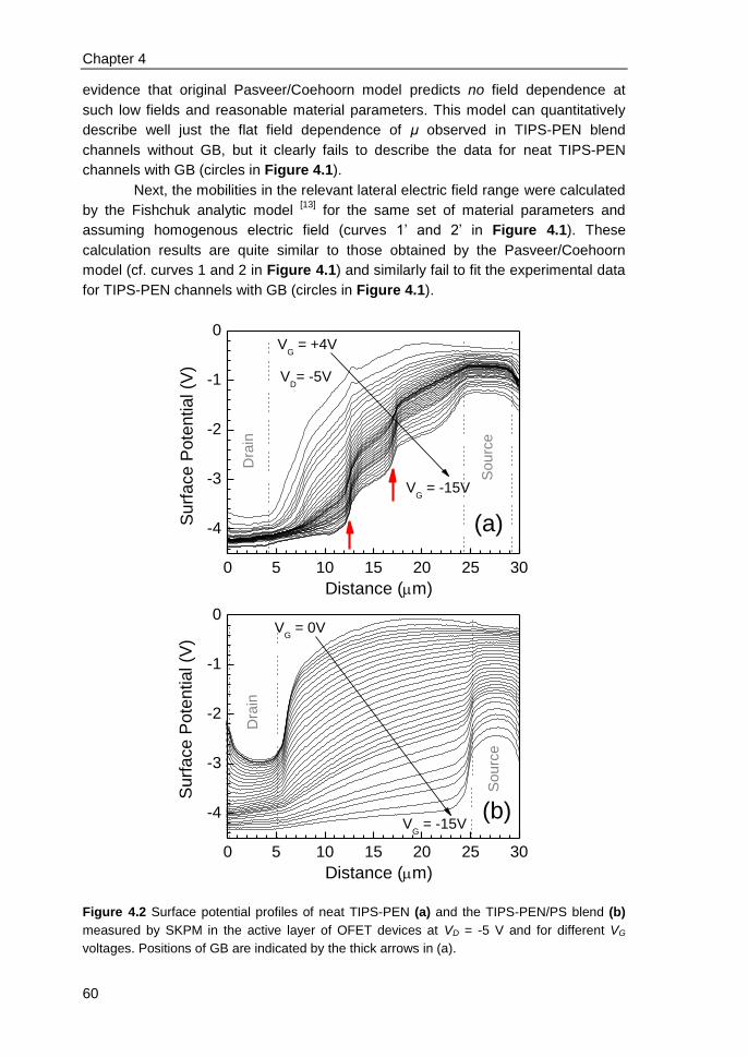
Chapter 4
60
evidence that original Pasveer/Coehoorn model predicts no field dependence at
such low fields and reasonable material parameters. This model can quantitatively
describe well just the flat field dependence of μ observed in TIPS-PEN blend
channels without GB, but it clearly fails to describe the data for neat TIPS-PEN
channels with GB (circles in Figure 4.1).
Next, the mobilities in the relevant lateral electric field range were calculated
by the Fishchuk analytic model [13]
for the same set of material parameters and
assuming homogenous electric field (curves 1’ and 2’ in Figure 4.1). These
calculation results are quite similar to those obtained by the Pasveer/Coehoorn
model (cf. curves 1 and 2 in Figure 4.1) and similarly fail to fit the experimental data
for TIPS-PEN channels with GB (circles in Figure 4.1).
0 5 10 15 20 25 30
-4
-3
-2
-1
0
0 5 10 15 20 25 30
-4
-3
-2
-1
0
(b)
Dra
in
So
urc
e
VG = +4V
Surf
ace P
ote
ntial (V
)
Distance (m)
VD= -5V
VG = -15V
(a)
Fig. 2
Surf
ace P
ote
ntial (V
)
So
urc
e
Dra
in
Distance (m)
VG = -15V
VG = 0V
Figure 4.2 Surface potential profiles of neat TIPS-PEN (a) and the TIPS-PEN/PS blend (b)
measured by SKPM in the active layer of OFET devices at VD = -5 V and for different VG
voltages. Positions of GB are indicated by the thick arrows in (a).
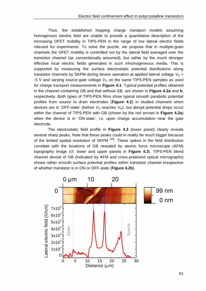
Electric field confinement effect in polycrystalline transistors
61
Thus, the established hopping charge transport models assuming
homogenous electric field are unable to provide a quantitative description of the
increasing OFET mobility in TIPS-PEN in the range of low lateral electric fields
relevant for experiments. To solve the puzzle, we propose that in multiple-grain
channels the OFET mobility is controlled not by the lateral field averaged over the
transistor channel (as conventionally assumed), but rather by the much stronger
effective local electric fields generated in such inhomogeneous media. This is
supported by measuring the surface electrostatic potential distributions along
transistor channels by SKPM during device operation at applied lateral voltage VD =
-5 V and varying source-gate voltage VG on the same TIPS-PEN samples as used
for charge transport measurements in Figure 4.1. Typical potential profiles obtained
in the channel containing GB and that without GB, are shown in Figure 4.2a and b,
respectively. Both types of TIPS-PEN films show typical smooth parabolic potential
profiles from source to drain electrodes (Figure 4.2) in studied channels when
devices are in ‘OFF-state’ (before VG reaches Vth), but abrupt potential drops occur
within the channel of TIPS-PEN with GB (shown by the red arrows in Figure 4.2a)
when the device is in ‘ON-state’, i.e. upon charge accumulation near the gate
electrode.
The electrostatic field profile in Figure 4.3 (lower panel) clearly reveals
several sharp peaks. Note that these peaks could in reality be much bigger because
of the limited spatial resolution of SKPM [30]
. These spikes in the field distribution
correlate with the locations of GB revealed by atomic force microscope (AFM)
topography image (cf. lower and upper panels in Figure 4.3). TIPS-PEN blend
channel devoid of GB (indicated by AFM and cross-polarized optical micrographs)
shows rather smooth surface potential profiles within transistor channel irrespective
of whether transistor is in ON or OFF-state (Figure 4.2b).
0 5 10 15 20 25 30
0
1x10³
2x10³
3x10³
4x10³
5x10³
6x10³
7x10³
Sourc
e
Dra
in
Fig. 3
La
tera
l e
lectr
ic f
ield
(V
/cm
)
Distance (m)
Chapter 4
62
Figure 4.3 Lower panel: distribution of lateral electric field calculated from the surface
potential distribution from Figure 4.2 (a) at VD = -5 V and VG = -15 V in neat TIPS-PEN
channel. Positions of GB are indicated by blue arrows. Upper panel: corresponding AFM
topography image of the studied channel. Red horizontal line in the upper panel depicts the
position where the cross-section of SKPM scan in Figure 4.2a was taken.
Strong inhomogeneity of lateral electric field in the conductive channel can
be rationalized in terms of electrostatic screening due to different local conductivities
within grains and at GB. GB are known to limit charge transport in polycrystalline
films by establishing major potential barriers [22][31][32][33]
between their more ordered
domains. In such cases the OFET conductive channel can be considered as a
series of resistors whose resistance is controlled by the ‘microscopic’ charge
mobility. In the OFF-state the lateral field is homogenous because the dielectric
constant is virtually isotropic. Therefore μ is isotropic. Upon applying a gate voltage
to a channel with GB, charges (holes) start to accumulate in the channel, and
instantaneously the density of accumulated holes within an individual grain is
redistributed along the external lateral field (source to drain) direction: at one side of
the grain it generates a locally increased hole concentration, and at the other side a
reduced (or close to locally ‘depleted’) hole density. This creates an internal lateral
electric field within the individual grain which compensates the applied external field.
Note that this ‘charge-redistribution’ effect stems from the mobile (not trapped) holes
inside grains induced by VG voltage, therefore here termed as a charge
accumulation (rather than trapping) process at the grain boundary. This effect
generates high local field between the grains (i.e. at the GB), while the field inside
the grains is screened. This would translate into an inhomogeneity of the lateral
electric field. As long as the spatial extension of GB is much smaller than the
average size of more ordered grains, the local fields could be much stronger than
the average applied field.
The concept of inhomogeneous local fields can describe ‘quantitatively’ the
experimentally observed lateral-field dependence of the OFET mobility by slightly
modifying either the Pasveer/Coehoorn model or the Fishchuk model. The barrier
heights due to GB are subject to distribution over the film, therefore taking into
account a huge variety of percolative passes present between the long source and
drain electrodes, the charge transport in average could be considered as that
occurring in an effectively random disordered system even though charge carriers
may experience just a few crossings over GB in a particular percolative pass. Since
the actual ratio between local field at the GB and the averaged field is not amenable
to analytical treatment, we will introduce a phenomenological field magnification
parameter q >> 1 as a fitting parameter (see Appendix of this Chapter for the thus-
modified Pasveer/Coehoorn model, with the field magnification parameter q
implemented into the original equations). Evidently that employment of q parameter
just results in renormalization of the electric field F used in our calculations.
Figure 4.1 demonstrates that the experimental results on the field
dependence of μ in TIPS-PEN channels with GB (Figure 4.1, circles) can be well
Electric field confinement effect in polycrystalline transistors
63
fitted using q = 64 and q = 115 for the Fishchuk (Figure 4.1, red curve 3’) and the
Pasveer/Coehoorn (Figure 4.1, blue curve 3) model, respectively, using the same σ
= 73 meV. The flat lateral-field dependence observed in channels without GB
(Figure 4.1, squares) is also well described by our model assuming the absence of
strong local fields (q = 1) in the homogenous film using a smaller energetic disorder
parameter σ = 65 meV.
4.4 Conclusions
In conclusion, by disentangling the effect of lateral field from carrier density,
we have observed an unexpected field dependence of the charge carrier mobility in
an organic field-effect transistor at low electric fields. It is a signature of a
phenomenon that could be termed as electric-field confinement effect in a grainy
organic film and this concept can ‘quantitatively’ describe the experimentally
observed lateral-field dependence of the OFET mobility with modified hopping
transport models. It originates from a lateral redistribution of accumulated (gate-
induced) mobile charges by the applied source-drain voltage, at the grain
boundaries. It gives rise to strong local electric field and is relevant for organic films
with inhomogeneous morphology caused by e.g. sample annealing in order to
improve charge transport, and for chemically doped organic polycrystalline films.
4.5 References
[1] H. Klauk, Organic Electronics: Materials, Manufacturing and Applications, Wiley-vch, Weinheim 2006.
[2] M. Berggren, D. Nilsson, N.D. Robinson, Nat. Mater. 2007, 6, 3–5. [3] W. Warta, N. Karl, Phys. Rev. B 1985, 32, 1172–1182. [4] W. Warta, R. Stehle, N. Karl, Appl. Phys. A: Solids Surf. 1985, A36, 163–170. [5] H. Bässler, Phys. Stat. Sol. (b) 1993, 175, 15–56. [6] P.M. Borsenberger, D.S. Weiss, Organic Photoreceptors for Xerography,
Marcel Dekker, New York 1998. [7] Y.N. Gartstein, E.M. Conwell, Chem. Phys. Lett. 1995, 245, 351–358. [8] S.V. Novikov, D.H. Dunlap, V.M. Kenkre, P.E. Parris, A.V. Vannikov, Phys.
Rev. Lett. 1998, 81, 4472–4475. [9] W.F. Pasveer, J. Cottaar, C. Tanase, R. Coehoorn, P.A. Bobbert, P.W.M.
Blom, D.M. de Leeuw, M.A.J. Michels, Phys. Rev. Lett. 2005, 94, 206601. [10] R. Coehoorn, W.F. Pasveer, P.A. Bobbert, M.A.J. Michels, Phys. Rev. B
2005, 72, 155206. [11] V.I. Arkhipov, P. Heremans, E.V. Emelianova, G.J. Adriaenssens, H. Bässler,
J. Phys.: Condens. Matter 2002, 14, 9899–9911. [12] I.I. Fishchuk, V.I. Arkhipov, A. Kadashchuk, P. Heremans, H. Bässler, Phys.
Rev. B 2007, 76, 045210. [13] I.I. Fishchuk, A.K. Kadashchuk, M. Ullah, H. Sitter, A. Pivrikas, J. Genoe, H.
Bässler, submitted to Phys. Rev. B. [14] M. Bouhassoune, S.L.M. van Mensfoort, P.A. Bobbert, R. Coehoorn, Org.
Electron. 2009, 10, 437–445.

Chapter 4
64
[15] X. Li, W.T.T. Smaal, C. Kjellander, B. van der Putten, K. Gualandris, E.C.P. Smits, J. Anthony, D.J. Broer, P.W.M. Blom, J. Genoe, G. Gelinck, Org. Electron. 2011, 12, 1319–1327.
[16] J.E. Anthony, J.S. Brooks, D.L. Eaton, S.R. Parkin, J. Am. Chem. Soc. 2001, 123, 9482–9483.
[17] S.M. Sze, Physics of Semiconductor Devices, 2nd Ed., Wiley, New York 1981.
[18] Y.P. Tsividis, Operation and Modeling of the MOS Transistor, Chapter 4, 2nd Ed., Mcgraw-hill, New York 1999.
[19] A. Bolognesi, A. Di Carlo, P. Lugli, Appl. Phys. Lett. 2002, 81, 4646–4648. [20] S. Scheinert, G. Paasch, Phys. Stat. Sol. (a) 2004, 201, 1263–1301. [21] Y. Luo, F. Gustavo, J.-Y. Henry, F. Mathevet, F. Lefloch, M. Sanquer, P.
Rannou, B. Grévin, Adv. Mater. 2007, 19, 2267–2273. [22] L.C. Teague, B.H. Hamadani, O.D. Jurchescu, S. Subramanian, J.E.
Anthony, T.N. Jackson, C.A. Richter, D.J. Gundlach, J.G. Kushmerick, Adv. Mater. 2008, 20, 4513–4516.
[23] L.C. Teague, O.D. Jurchescu, C.A. Richter, S. Subramanian, J.E. Anthony, T.N. Jackson, D.J. Gundlach, J.G. Kushmerick, Appl. Phys. Lett. 2010, 96, 203305.
[24] S. van Reenen, P. Matyba, A. Dzwilewski, R.A.J. Janssen, L. Edman, M. Kemerink, Adv. Funct. Mater. 2011, 21, 1795–1802.
[25] T. Ohe, M. Kuribayashi, R. Yasuda, A. Tsuboi, K. Nomoto, K. Satori, M. Itabashi, J. Kasahara, Appl. Phys. Lett. 2008, 93, 053303.
[26] Y.S. Chung, N. Shin, J. Kang, Y. Jo, V.M. Prabhu, S.K. Satija, R.J. Kline, D.M. DeLongchamp, M.F. Toney, M.A. Loth, B. Purushothaman, J.E. Anthony, D.Y. Yoon, J. Am. Chem. Soc. 2011, 133, 412–415.
[27] S. Verlaak, P. Heremans, Phys. Rev. B 2007, 75, 115127. [28] I.I. Fishchuk, A.K. Kadashchuk, J. Genoe, M. Ullah, H. Sitter, T.B. Singh,
N.S. Sariciftci, H. Bässler, Phys. Rev. B 2010, 81, 045202. [29] J.G. Park, R. Vasic, J.S. Brooks, J.E. Anthony, J. Appl. Phys. 2006, 100,
044511. [30] D. Charrier, M. Kemerink, B. Smalbrugge, T. de Vries, R. Janssen, ACS
Nano 2008, 2, 622–626. [31] G. Horowitz, M.E. Hajlaoui, R. Hajlaoui, J. Appl. Phys. 2000, 87, 4456–4463. [32] L.G. Kaake, P.F. Barbara, X.-Y. Zhu, J. Phys. Chem. Lett. 2010, 1, 628–635. [33] P. Annibale, C. Albonetti, P. Stoliar, F. Biscarini, J. Phys. Chem. A 2007, 111,
12854–12858.

Electric field confinement effect in polycrystalline transistors
65
Appendix
Modified Pasveer/Coehoorn model with a field magnification parameter (q):
Based on numerical simulations of charge transport in Gaussian density-of-
states (DOS), Pasveer and Coehoorn [1][2]
suggested a parameterization scheme to
obtain the dependence of the charge-carrier mobility on temperature, carrier density,
and electric field. In Chapter 4 above we introduced a phenomenological field
magnification parameter (q) to their original equations [1]
, as shown below:
FTfcuTFcT ,])2(exp[),,( 0
, (4A.1)
where TkB
ˆ ;
0
2
0
ea ;
2
ˆˆ 2 u ;
2
2
ˆ
4lnlnˆˆln2
v ;
2
0
9
0ˆ42.0exp108.1 T ;
and
18.012.2ˆ44.0exp,
2
23
eaqFFTf .
In this modified equation, in the expression of f(T,F) in (4A.1), q is the field
magnification parameter (in the original Pasveer/Coehoorn model q = 1); σ is the
width of the DOS, kB is the Boltzmann constant, a is average intersite distance, b is
the localization radius of a charge carrier, 0 is a frequency factor, c = n / N is the
relative carrier concentration with respect to the concentration of localized states N,
and e is the elementary charge.
References:
[1] W.F. Pasveer, J. Cottaar, C. Tanase, R. Coehoorn, P.A. Bobbert, P.W.M. Blom, D.M. de Leeuw, M.A.J. Michels, Phys. Rev. Lett. 2005, 94, 206601.
[2] R. Coehoorn, W.F. Pasveer, P.A. Bobbert, M.A.J. Michels, Phys. Rev. B 2005, 72, 155206.
66
CHAPTER V
5. Solution-processed small molecule
transistors with low operating
voltages and high grain-boundary
anisotropy
In this chapter, we use molecular design to control the morphology and molecular
order of organic semiconductors. We present a new soluble pentacene derivative
with ethyl substitutions in the 2,3,9,10 backbone positions to modulate the solubility
and film forming properties of this material compared to triisopropylsilylethynyl
pentacene (TIPS-PEN). This permits reproducible production of molecularly highly
ordered structures that feature average transistor mobilities in excess of 1 cm2/Vs
depending on crystal orientation by careful selection of casting conditions.
Published as:
L. Yu, X. Li, J. Smith, S. Tierney, R. Sweeney, B.K.C. Kjellander, G.H. Gelinck, T.D.
Anthopoulos, N. Stingelin, J. Mater. Chem. 2012, 22, 9458–9461.
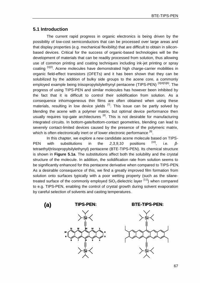
BTE-TIPS-PEN
67
5.1 Introduction
The current rapid progress in organic electronics is being driven by the
possibility of low-cost semiconductors that can be processed over large areas and
that display properties (e.g. mechanical flexibility) that are difficult to obtain in silicon-
based devices. Critical for the success of organic-based technologies will be the
development of materials that can be readily processed from solution, thus allowing
use of common printing and coating techniques including ink-jet printing or spray
coating [1][2]
. Acene molecules have demonstrated high charge-carrier mobilities in
organic field-effect transistors (OFETs) and it has been shown that they can be
solubilized by the addition of bulky side groups to the acene core, a commonly
employed example being triisopropylsilylethynyl pentacene (TIPS-PEN) [3][4][5][6]
. The
progress of using TIPS-PEN and similar molecules has however been inhibited by
the fact that it is difficult to control their solidification from solution. As a
consequence inhomogeneous thin films are often obtained when using these
materials, resulting in low device yields [7]
. This issue can be partly solved by
blending the acene with a polymer matrix, but optimal device performance then
usually requires top-gate architectures [8]
. This is not desirable for manufacturing
integrated circuits. In bottom-gate/bottom-contact geometries, blending can lead to
severely contact-limited devices caused by the presence of the polymeric matrix,
which is often electronically inert or of lower electronic performance [9]
.
In this chapter, we explore a new candidate acene molecule based on TIPS-
PEN with substitutions in the 2,3,9,10 positions [10]
, i.e. β-
tetraethyl(triisopropylsilylethynyl) pentacene (BTE-TIPS-PEN). Its chemical structure
is shown in Figure 5.1a. The substitutions affect both the solubility and the crystal
structure of the molecule. In addition, the solidification rate from solution seems to
be significantly enhanced for this pentacene derivative when compared to TIPS-PEN.
As a desirable consequence of this, we find a greatly improved film formation from
solution onto surfaces typically with a poor wetting property (such as the silane-
treated surface of the commonly employed SiO2 dielectric layer [11]
) when compared
to e.g. TIPS-PEN, enabling the control of crystal growth during solvent evaporation
by careful selection of solvents and casting temperatures.
Si
Si
2
3
45678
114131211
10
9
Si
Si
Si
Si
2
3
2
3
45678
114131211
10
9
10
9
Si
Si
Si
Si
BTE-TIPS-PEN:TIPS-PEN:(a)
Si
Si
2
3
45678
114131211
10
9
Si
Si
Si
Si
2
3
2
3
45678
114131211
10
9
10
9
Si
Si
Si
Si
BTE-TIPS-PEN:TIPS-PEN:(a)
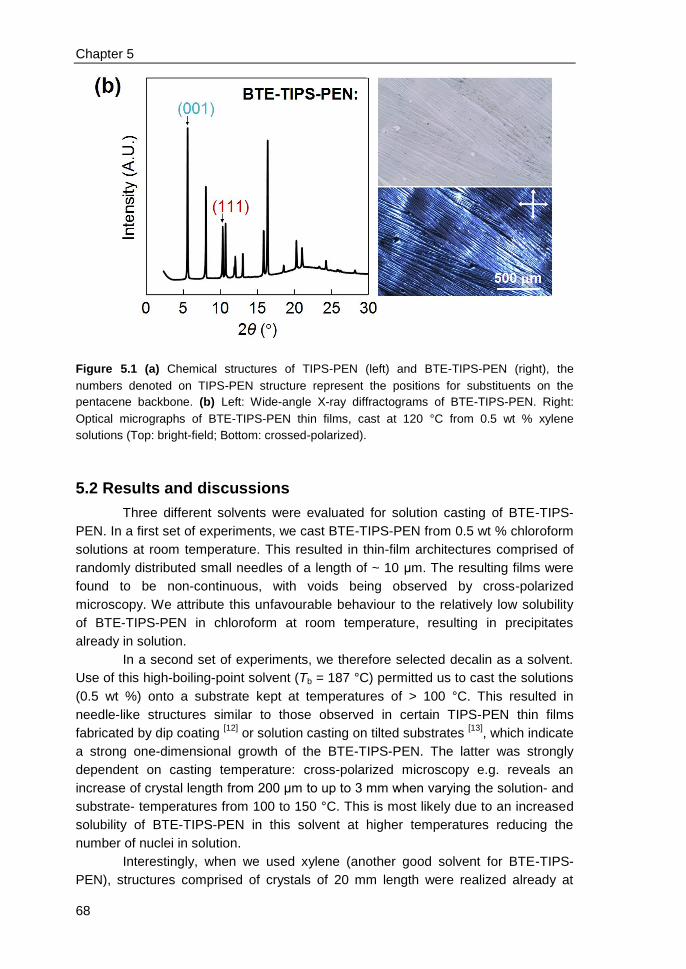
Chapter 5
68
Figure 5.1 (a) Chemical structures of TIPS-PEN (left) and BTE-TIPS-PEN (right), the
numbers denoted on TIPS-PEN structure represent the positions for substituents on the
pentacene backbone. (b) Left: Wide-angle X-ray diffractograms of BTE-TIPS-PEN. Right:
Optical micrographs of BTE-TIPS-PEN thin films, cast at 120 °C from 0.5 wt % xylene
solutions (Top: bright-field; Bottom: crossed-polarized).
5.2 Results and discussions
Three different solvents were evaluated for solution casting of BTE-TIPS-
PEN. In a first set of experiments, we cast BTE-TIPS-PEN from 0.5 wt % chloroform
solutions at room temperature. This resulted in thin-film architectures comprised of
randomly distributed small needles of a length of ~ 10 μm. The resulting films were
found to be non-continuous, with voids being observed by cross-polarized
microscopy. We attribute this unfavourable behaviour to the relatively low solubility
of BTE-TIPS-PEN in chloroform at room temperature, resulting in precipitates
already in solution.
In a second set of experiments, we therefore selected decalin as a solvent.
Use of this high-boiling-point solvent (Tb = 187 °C) permitted us to cast the solutions
(0.5 wt %) onto a substrate kept at temperatures of > 100 °C. This resulted in
needle-like structures similar to those observed in certain TIPS-PEN thin films
fabricated by dip coating [12]
or solution casting on tilted substrates [13]
, which indicate
a strong one-dimensional growth of the BTE-TIPS-PEN. The latter was strongly
dependent on casting temperature: cross-polarized microscopy e.g. reveals an
increase of crystal length from 200 μm to up to 3 mm when varying the solution- and
substrate- temperatures from 100 to 150 °C. This is most likely due to an increased
solubility of BTE-TIPS-PEN in this solvent at higher temperatures reducing the
number of nuclei in solution.
Interestingly, when we used xylene (another good solvent for BTE-TIPS-
PEN), structures comprised of crystals of 20 mm length were realized already at
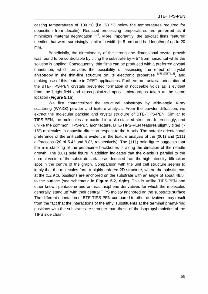
BTE-TIPS-PEN
69
casting temperatures of 100 °C (i.e. 50 °C below the temperatures required for
deposition from decalin). Reduced processing temperatures are preferred as it
minimizes material degradation [14]
. More importantly, the as-cast films featured
needles that were surprisingly similar in width (~ 5 μm) and had lengths of up to 20
mm.
Beneficially, the directionality of the strong one-dimensional crystal growth
was found to be controllable by tilting the substrate by ~ 5° from horizontal while the
solution is applied. Consequently, thin films can be produced with a preferred crystal
orientation, which provides the possibility of assessing the effect of crystal
anisotropy in the thin-film structure on its electronic properties [15][16][17][18]
, and
making use of this feature in OFET applications. Furthermore, uniaxial orientation of
the BTE-TIPS-PEN crystals prevented formation of noticeable voids as is evident
from the bright-field and cross-polarized optical micrographs taken at the same
location (Figure 5.1b).
We first characterized the structural anisotropy by wide-angle X-ray
scattering (WAXS) powder and texture analysis. From the powder diffraction, we
extract the molecular packing and crystal structure of BTE-TIPS-PEN. Similar to
TIPS-PEN, the molecules are packed in a slip-stacked structure. Interestingly, and
unlike the common TIPS-PEN architecture, BTE-TIPS-PEN features slightly tilted (~
15°) molecules in opposite direction respect to the b-axis. The notable orientational
preference of the unit cells is evident in the texture analysis of the (001) and (111)
diffractions (2θ of 5.4° and 9.8°, respectively). The (111) pole figure suggests that
the π-π stacking of the pentacene backbones is along the direction of the needle
growth. The (001) pole figure in addition indicates that the c-axis is parallel to the
normal vector of the substrate surface as deduced from the high intensity diffraction
spot in the centre of the graph. Comparison with the unit cell structure seems to
imply that the molecules form a highly ordered 2D-structure, where the substituents
at the 2,3,9,10 positions are anchored on the substrate with an angle of about 48.8°
to the surface (see schematic in Figure 5.2, right). This is unlike TIPS-PEN and
other known pentacene and anthradithiophene derivatives for which the molecules
generally ‘stand up’ with their central TIPS moiety anchored on the substrate surface.
The different orientation of BTE-TIPS-PEN compared to other derivatives may result
from the fact that the interactions of the ethyl substituents at the terminal phenyl-ring
positions with the substrate are stronger than those of the isopropyl moieties of the
TIPS side chain.
Chapter 5
70
Figure 5.2 (Left) Wide-angle X-ray diffraction (001) and (111) pole figures of BTE-TIPS-PEN
thin films. (Right) Schematic of the unit cell of BTE-TIPS-PEN structures and its orientation
with respect to the substrate (the red arrow indicates the growth direction of the needles).
Black circle in the pole figure of (111) diffraction indicates the direction of ψ = 42.3° and φ =
48.8°.
To evaluate the influence of different needle orientation in terms of
electronic behaviour, we fabricated bottom-gate/bottom-contact OFETs on Si
(n++)/SiO2 substrates with an oxide thickness of 140 nm and photolithographically
patterned Au as source and drain electrodes. Prior to device fabrications, a
pentafluorobenzenethiol monolayer was deposited on Au electrodes [19]
. The SiO2
dielectric was treated with trichlorophenylsilane [20][21][22]
.
The as-cast thin films comprised of uniaxially aligned BTE-TIPS-PEN
needles exhibited excellent transistor performance. The transfer characteristics of
two typical devices (with identical channel width to length ratio, W/L) are shown in
Figure 5.3a. We compare the two extreme cases of needle orientation, i.e. OFETs
with the BTE-TIPS-PEN needle directions being positioned parallel or perpendicular
to the direction of the source-drain bias. It is evident from the data displayed in
Figure 5.3a that both structures result in transistors that are operating at remarkably
low voltages (< 5 V) and that display negligible hysteresis between the forward and
backward sweeps. For OFETs based on BTE-TIPS-PEN needles positioned parallel
to the source-drain bias direction, we find an average saturation mobility of 1.34
cm2/Vs, which is combined with an on/off ratio of over 10
5, a near-zero threshold
voltage, and a steep sub-threshold slope (~ 130 mV/dec). The latter value compares
indeed favourably with some of the lowest reported values for organic transistors [9][23][24][25]
, suggesting a high quality gate-dielectric/semiconductor interface with few
charge-trapping centres [26][27]
. Clearly, interfacial trapping is not adversely mitigating
charge-transport in these devices. In comparison, devices with BTE-TIPS-PEN
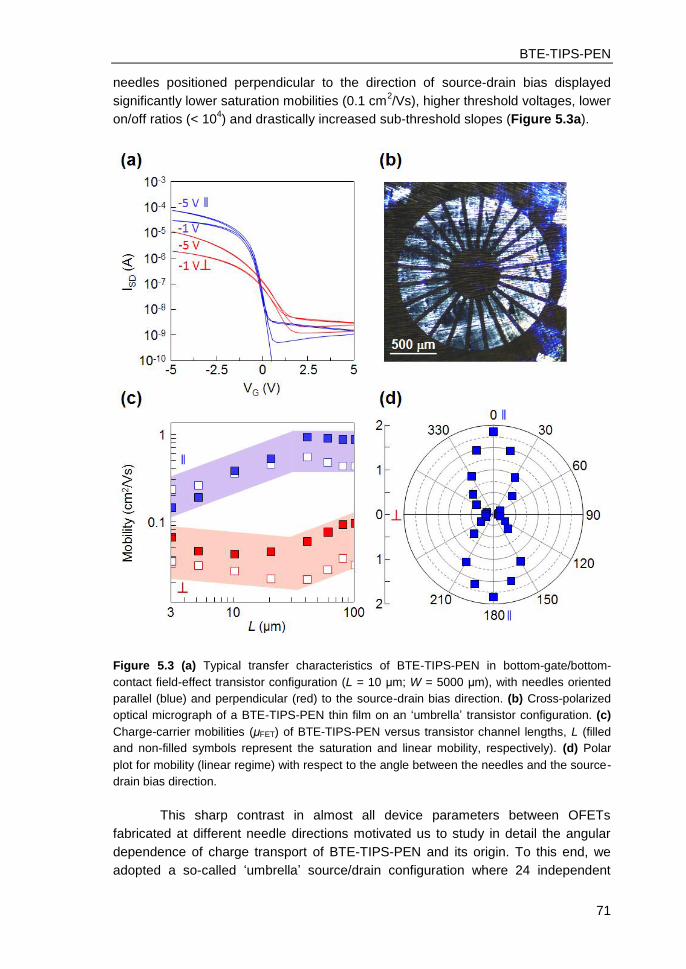
BTE-TIPS-PEN
71
needles positioned perpendicular to the direction of source-drain bias displayed
significantly lower saturation mobilities (0.1 cm2/Vs), higher threshold voltages, lower
on/off ratios (< 104) and drastically increased sub-threshold slopes (Figure 5.3a).
Figure 5.3 (a) Typical transfer characteristics of BTE-TIPS-PEN in bottom-gate/bottom-
contact field-effect transistor configuration (L = 10 μm; W = 5000 μm), with needles oriented
parallel (blue) and perpendicular (red) to the source-drain bias direction. (b) Cross-polarized
optical micrograph of a BTE-TIPS-PEN thin film on an ‘umbrella’ transistor configuration. (c)
Charge-carrier mobilities (μFET) of BTE-TIPS-PEN versus transistor channel lengths, L (filled
and non-filled symbols represent the saturation and linear mobility, respectively). (d) Polar
plot for mobility (linear regime) with respect to the angle between the needles and the source-
drain bias direction.
This sharp contrast in almost all device parameters between OFETs
fabricated at different needle directions motivated us to study in detail the angular
dependence of charge transport of BTE-TIPS-PEN and its origin. To this end, we
adopted a so-called ‘umbrella’ source/drain configuration where 24 independent
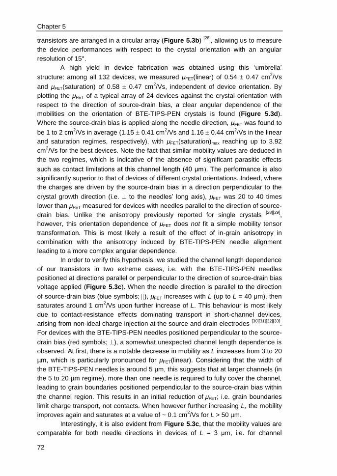
Chapter 5
72
transistors are arranged in a circular array (Figure 5.3b) [28]
, allowing us to measure
the device performances with respect to the crystal orientation with an angular
resolution of 15°.
A high yield in device fabrication was obtained using this ‘umbrella’
structure: among all 132 devices, we measured μFET(linear) of 0.54 0.47 cm2/Vs
and μFET(saturation) of 0.58 0.47 cm2/Vs, independent of device orientation. By
plotting the μFET of a typical array of 24 devices against the crystal orientation with
respect to the direction of source-drain bias, a clear angular dependence of the
mobilities on the orientation of BTE-TIPS-PEN crystals is found (Figure 5.3d).
Where the source-drain bias is applied along the needle direction, μFET was found to
be 1 to 2 cm2/Vs in average (1.15 0.41 cm
2/Vs and 1.16 0.44 cm
2/Vs in the linear
and saturation regimes, respectively), with μFET(saturation)max reaching up to 3.92
cm2/Vs for the best devices. Note the fact that similar mobility values are deduced in
the two regimes, which is indicative of the absence of significant parasitic effects
such as contact limitations at this channel length (40 μm. The performance is also
significantly superior to that of devices of different crystal orientations. Indeed, where
the charges are driven by the source-drain bias in a direction perpendicular to the
crystal growth direction (i.e. to the needles’ long axis), μFET was 20 to 40 times
lower than μFET measured for devices with needles parallel to the direction of source-
drain bias. Unlike the anisotropy previously reported for single crystals [28][29]
,
however, this orientation dependence of μFET does not fit a simple mobility tensor
transformation. This is most likely a result of the effect of in-grain anisotropy in
combination with the anisotropy induced by BTE-TIPS-PEN needle alignment
leading to a more complex angular dependence.
In order to verify this hypothesis, we studied the channel length dependence
of our transistors in two extreme cases, i.e. with the BTE-TIPS-PEN needles
positioned at directions parallel or perpendicular to the direction of source-drain bias
voltage applied (Figure 5.3c). When the needle direction is parallel to the direction
of source-drain bias (blue symbols; ), μFET increases with L (up to L = 40 μm), then
saturates around 1 cm2/Vs upon further increase of L. This behaviour is most likely
due to contact-resistance effects dominating transport in short-channel devices,
arising from non-ideal charge injection at the source and drain electrodes [30][31][32][33]
.
For devices with the BTE-TIPS-PEN needles positioned perpendicular to the source-
drain bias (red symbols; ), a somewhat unexpected channel length dependence is
observed. At first, there is a notable decrease in mobility as L increases from 3 to 20
µm, which is particularly pronounced for μFET(linear). Considering that the width of
the BTE-TIPS-PEN needles is around 5 μm, this suggests that at larger channels (in
the 5 to 20 µm regime), more than one needle is required to fully cover the channel,
leading to grain boundaries positioned perpendicular to the source-drain bias within
the channel region. This results in an initial reduction ofμFET; i.e. grain boundaries
limit charge transport, not contacts. When however further increasing L, the mobility
improves again and saturates at a value of ~ 0.1 cm2/Vs for L > 50 µm.
Interestingly, it is also evident from Figure 5.3c, that the mobility values are
comparable for both needle directions in devices of L = 3 μm, i.e. for channel
BTE-TIPS-PEN
73
dimensions smaller than the width of the grains. This indicates that there is a
relatively low intrinsic in-grain anisotropy of μFET (~ 2 and 4 in the saturation and
linear regimes, respectively), suggesting that more pronounced anisotropy effects
arise due to the presence of grain boundaries within the channel region at specific
needle orientations. Hence, the high μFET anisotropy is mainly attributed to the
geometric morphology (i.e. anisotropy of number of grain-boundaries [12][34]
) of the
BTE-TIPS-PEN needles.
5.3 Conclusions
In summary, we have demonstrated that BTE-TIPS-PEN – a new TIPS-PEN
derivative with substituents in the 2,3,9,10 positions of the pentacene backbone –
can be readily fabricated into high-performance OFET structures using a single-step
process without the need to form blends or use of top-gate structures. Average
mobilities of more than 1 cm2/Vs are measured in both linear and saturation regimes
(at source-drain biases of -1 V and -5 V, respectively) for specific crystal orientations,
with the highest saturation mobility measured in these devices being as high as 3.92
cm2/Vs. This performance is a notable improvement over TIPS-PEN previously
produced by drop-casting, spin-coating, and ink-jet printing [35]
, and other solution-
processed acene-based single component devices [36][37][38]
, confirming that
improved molecular engineering results in a controlled micro- and macro-structure of
BTE-TIPS-PEN thin films that is positively influencing the electronic properties. This
is realized with a high level of reproducibility, required for the technological
exploitation of such discrete devices in large-area organic electronics. In addition, a
complex angular dependence of mobilities was observed for BTE-TIPS-PEN films
cast from xylene comprising needles of up to 20 mm in length (5 μm in width), the
origin of which is attributed to a combined effect of in-grain anisotropy in conjunction
with the anisotropy given by the BTE-TIPS-PEN needles, resulting in different
amounts of grain boundaries depending on the crystal orientation.
5.4 References
[1] B.J. de Gans, P.C. Duineveld, U.S. Schubert, Adv. Mater. 2004, 16, 203–213.
[2] N.A. Azarova, J.W. Owen, C.A. McLellan, M.A. Grimminger, E.K. Chapman, J.E. Anthony, O.D. Jurchescu, Org. Electron. 2010, 11, 1960–1965.
[3] J.E. Anthony, J.S. Brooks, D.L. Eaton, S.R. Parkin, J. Am. Chem. Soc. 2001, 123, 9482–9483.
[4] C.D. Sheraw, T.N. Jackson, D.L. Eaton, J.E. Anthony, Adv. Mater. 2003, 15, 2009–2011.
[5] S.K. Park, T.N. Jackson, J.E. Anthony, D.A. Mourey, Appl. Phys. Lett. 2007, 91, 063514.
[6] G. Giri, E. Verploegen, S.C.B. Mannsfeld, S. Atahan-Evrenk, D.H. Kim, S.Y. Lee, H.A. Becerril, A. Aspuru-Guzik, M.F. Toney, Z. Bao, Nature 2011, 480, 504–508.
Chapter 5
74
[7] J.H. Chen, D.C. Martin, J.E. Anthony, J. Mater. Res. 2007, 22, 1701–1709. [8] R. Hamilton, J. Smith, S. Ogier, M. Heeney, J.E. Anthony, I. McCulloch, J.
Veres, D.D.C. Bradley, T.D. Anthopoulos, Adv. Mater. 2009, 21, 1166–1171. [9] X. Li, W.T.T. Smaal, C. Kjellander, B. van der Putten, K. Gualandris, E.C.P.
Smits, J. Anthony, D.J. Broer, P.W.M. Blom, J. Genoe, G. Gelinck, Org. Electron. 2011, 12, 1319–1327.
[10] J. Jiang, B.R. Kaafarani, D.C. Neckers, J. Org. Chem. 2006, 71, 2155–2158. [11] H. Ma, H. Yip, F. Huang, A.K.Y. Jen, Adv. Funct. Mater. 2010, 20, 1371–
1388. [12] C.W. Sele, B.K.C. Kjellander, B. Niesen, M.J. Thornton, J.B.P.H. van der
Putten, K. Myny, H.J. Wondergem, A. Moser, R. Resel, A.J.J.M. van Breemen, N. van Aerle, P. Heremans, J.E. Anthony, G.H. Gelinck, Adv. Mater. 2009, 21, 4926–4931.
[13] W.H. Lee, D.H. Kim, Y. Jang, J.H. Cho, M. Hwang, Y.D. Park, Y.H. Kim, J.I. Han, K. Cho, Appl. Phys. Lett. 2007, 90, 132106.
[14] J.H. Chen, S. Subramanian, S.R. Parkin, M. Siegler, K. Gallup, C. Haughn, D.C. Martin, J.E. Anthony, J. Mater. Chem. 2008, 18, 1961–1969.
[15] B. O’Connor, R.J. Kline, B.R. Conrad, L.J. Richter, D. Gundlach, M.F. Toney, D.M. DeLongchamp, Adv. Funct. Mater. 2011, 21, 3697–3705.
[16] X. Zhang, L.J. Richter, D.M. DeLongchamp, R.J. Kline, M.R. Hammond, I. McCulloch, M. Heeney, R.S. Ashraf, J.N. Smith, T.D. Anthopoulos, B. Schroeder, Y.H. Geerts, D.A. Fischer, M.F. Toney, J. Am. Chem. Soc. 2011, 133, 15073–15084.
[17] A. Salleo, R.J. Kline, D.M. DeLongchamp, M.L. Chabinyc, Adv. Mater. 2010, 22, 3812–3838.
[18] I. McCulloch, M. Heeney, M.L. Chabinyc, D. DeLongchamp, R.J. Kline, M. Cölle, W. Duffy, D. Fischer, D. Gundlach, B. Hamadani, R. Hamilton, L. Richter, A. Salleo, M. Shkunov, D. Sparrowe, S. Tierney, W. Zhang, Adv. Mater. 2009, 21, 1091–1109.
[19] M.M. Payne, S.R. Parkin, J.E. Anthony, C.C. Kuo, T.N. Jackson, J. Am. Chem. Soc. 2005, 127, 4986–4987.
[20] D. Janssen, R. De Palma, S. Verlaak, P. Heremans, W. Dehaen, Thin Solid Films 2006, 515, 1433–1438.
[21] D. Kumaki, M. Yahiro, Y. Inoue, S. Tokito, Appl. Phys. Lett. 2007, 90, 133511.
[22] X. Li, B.K.C. Kjellander, J.E. Anthony, C.W.M. Bastiaansen, D.J. Broer, G.H. Gelinck, Adv. Funct. Mater. 2009, 19, 3610–3617.
[23] U. Zschieschang, M.J. Kang, K. Takimiya, T. Sekitani, T. Someya, T.W. Canzler, A. Werner, J. Blochwitz-Nimoth, H. Klauk, J. Mater. Chem. 2012, 22, 4273–4277.
[24] V. Podzorov, S.E. Sysoev, E. Loginova, V.M. Pudalov, M.E. Gershenson, Appl. Phys. Lett. 2003, 83, 3504–3506.
[25] M. Halik, H. Klauk, U. Zschieschang, G. Schmid, C. Dehm, M. Schutz, S. Maisch, F. Effenberger, M. Brunnbauer, F. Stellacci, Nature 2004, 431, 963–966.
[26] S.H. Kim, D. Choi, D.S. Chung, C. Yang, J. Jang, C.E. Park, S.-H.K. Park, Appl. Phys. Lett. 2008, 93, 113306.
[27] K. Myny, S. De Vusser, S. Steudel, D. Janssen, R. Muller, S. De Jonge, S. Verlaak, J. Genoe, P. Heremans, Appl. Phys. Lett. 2006, 88, 222103.
[28] C. Reese, Z. Bao, Adv. Mater. 2007, 19, 4535–4538. [29] V.C. Sundar, J. Zaumseil, V. Podzorov, E. Menard, R.L. Willett, T. Someya,
M.E. Gershenson, J.A. Rogers, Science 2004, 303, 1644–1646. [30] H. Sirringhaus, Adv. Mater. 2005, 17, 2411–2425.
BTE-TIPS-PEN
75
[31] E. Meijer, G. Gelinck, E. van Veenendaal, B. Huisman, D. de Leeuw, T. Klapwijk, Appl. Phys. Lett. 2003, 82, 4576–4578.
[32] L. Bu rgi, H. Sirringhaus, R.H. Friend, Appl. Phys. Lett. 2002, 80, 2913–2915. [33] R.A. Street, A. Salleo, Appl. Phys. Lett. 2002, 81, 2887–2889. [34] J. Rivnay, L.H. Jimison, J.E. Northrup, M.F. Toney, R. Noriega, S. Lu, T.J.
Marks, A. Facchetti, A. Salleo, Nat. Mater. 2009, 8, 952–958. [35] J.A. Lim, H.S. Lee, W.H. Lee, K. Cho, Adv. Funct. Mater. 2009, 19, 1515–
1525. [36] D.J. Gundlach, J.E. Royer, S.K. Park, S. Subramanian, O.D. Jurchescu, B.H.
Hamadani, A.J. Moad, R.J. Kline, L.C. Teague, O. Kirillov, C.A. Richter, J.G. Kushmerick, L.J. Richter, S.R. Parkin, T.N. Jackson, J.E. Anthony, Nat. Mater. 2008, 7, 216–221.
[37] G.R. Llorente, M.B. Dufourg-Madec, D.J. Crouch, R.G. Pritchard, S. Ogier, S.G. Yeates, Chem. Commun. 2009, 3059–3061.
[38] Q. Meng, H. Dong, W. Hu, D. Zhu, J. Mater. Chem. 2011, 21, 11708–11721.
76
CHAPTER VI
6. Influence of solid-state
microstructure on the electronic
performance of a small-molecule
organic semiconductor
In this chapter, we demonstrate that a careful selection of the casting temperature
alone can allow a rapid production of OFETs with uniform and reproducible device
performance over large areas. Based on a systematic investigation on the thermal
behaviour of 5,11-bis(triethyl silylethynyl) anthradithiophene (TES ADT), we will
present four distinctive solid-state phases of TES ADT exhibiting drastically different
charge-transport properties, deduced from OFET device characteristics
corroborated by Lateral Time-of-Flight (L-ToF) photoconductivity measurements.
The best-performing crystal polymorph of TES ADT is identified: when casting
solutions of TES ADT dissolved in chloroform at a substrate temperature of more
than 20 °C below its glass transition temperature, highly-crystalline and
homogeneous TES ADT thin films can be facilely produced in a single-step, without
the need for any post-depositions as previously reported, opening pathways towards
high-throughput and reliable fabrication of high-performance OFETs.
(To be) published as:
L. Yu, X. Li, E. Pavlica, M. A. Loth, J. E. Anthony, G. Bratina, C. Kjellander, G.
Gelinck, N. Stingelin, Appl. Phys. Lett. 2011, 99, 263304.
L. Yu, X. Li, E. Pavlica, F. Koch, G. Portale, M. A. Loth, J. E. Anthony, P. Smith, G.
Bratina, B. K. C. Kjellander, C. W. M. Bastiaansen, D. J. Broer, G. H. Gelinck, N.
Stingelin, 2012, submitted to Adv. Mater..
Microstructure vs. electronic performance of TES ADT
77
6.1 Introduction
Solution-processable organic π-conjugated small molecules have been
demonstrated to show a great potential as active elements in electronic devices
such as organic field-effect transistors (OFETs) [1][2][3]
, organic solar cells [4][5]
, and
light-emitting diodes [6][7]
. Thereby, 5,11-bis(triethylsilylethynyl) anthradithiophene
(TES ADT) is one of the most promising materials for transistor applications; it can
be readily synthesized at relatively large quantities [8][9]
and charge-carrier mobilities
as high as 1.3 cm2/Vs and on/off ratios of more than 10
6 have been demonstrated
using this small molecule in OFET devices [8][10]
.
The remarkable electronic performance of TES ADT is, however,
challenging to produce at high yield when the material is processed from solution.
Indeed, the OFET mobility values reported in literature cover six orders of
magnitudes [8][11][12][13]
. One reason for this discrepancy in device performance can at
least partially be attributed to the fact that charge transport in small molecular
organic semiconductors depends on the extent of the π-orbital overlap and, thus, the
solid-state order in such thin film structures [8][14][15][16]
. For TES ADT, the extent as
well as the fashion how the molecules pack in such architectures strongly depend on
the deposition method and conditions selected. For example, spin-coating yields
predominantly amorphous thin films where charge-transport is inevitably limited by
the poor molecular order [11]
. By contrast, solution casting (e.g. ‘drop casting’) often
results in highly crystalline structures – although, these do not necessarily display
good device performance. The reason for this is that the degree of crystallinity, the
crystalline quality and orientation, grain size, presence of grain boundaries as well
as other features such as film roughness, can strongly influence the OFET
characteristics [17][18][19][20][21]
.
Apart from the deposition techniques and conditions, clearly, many structural
factors of organic thin-film structures can in addition be manipulated by post-
deposition procedures, such as thermal [22][23]
and/or solvent annealing [24][25][26]
.
Applied on TES ADT, for example, various annealing techniques have resulted in
more uniform structures of good device performance. Aging – i.e. crystallization in
the solid state over time – at room temperature in vacuum for a period of 7 days or
more of spin-coated, predominantly amorphous TES ADT films (field-effect
transistor mobility μFET ≈ 0.0007 cm2/Vs) resulted, for instance, in homogeneous and
crystalline structures of μFET ≈ 0.06 cm2/Vs
[12]. Furthermore, solvent vapor annealing
has been demonstrated to produce similar crystalline TES ADT architectures with
improved electronic performance, with μFET reaching 0.11 cm2/Vs after exposure to
1,2-dichloroethane vapor [11][13]
.
Recent studies, furthermore, indicate that TES ADT forms different
polymorphs depending on the thermal history of a given structure [27]
. Chung et al.
observed, for instance, an endothermic transition in differential scanning calorimetry
(DSC), which was attributed to a solid-to-solid phase transition. Detailed information
on such different crystal forms and their corresponding OFET characteristics is,
however, still lacking. Herein we, thus, report a systematic investigation on the
Chapter 6
78
thermal behaviour of TES ADT, its different solid-state phases and their charge-
transport properties deduced from OFET device characteristics as well as lateral
time-of-flight (L-ToF) photoconductivity measurements. We identify the highest
performance TES ADT structure, opening pathways which should allow advancing
processing protocols that permit to exclusively induce this polymorph for reliable
fabrication of high-performance bottom-gate/bottom-contact transistors.
6.2 Experimental
5,11-bis(triethyl silylethynyl) anthradithiophene (TES ADT) was synthesized
according to literature [8]
. Thin films for structural analysis as well as electronic
characterizations were fabricated by dissolving TES ADT in chloroform (4 wt %),
followed by solution casting onto the corresponding substrate kept at 5 °C in
ambient conditions [10]
, and hereafter termed as the ‘as-cast’ phase.
Differential scanning calorimetry (DSC) measurements were conducted
under N2 atmosphere at a scan rate of 10 °C/min with a Mettler Toledo STARe
system DSC 1. Standard Mettler aluminum crucibles were used. The sample weight
was ~ 5 mg. Optical microscopy was carried out with an Olympus BX51 polarizing
microscope equipped with a Q-imaging Go-3 camera and a Mettler Toledo FP82HT
hot-stage. Variable temperature wide-angle X-ray scattering (WAXS) was performed
in the BM26-DUBBLE Dutch-Belgian beamline of the European Synchrotron
Radiation Facility (ESRF) with a Linkam THMS600 temperature-controlled stage.
The samples were in powder form obtained from the as-cast TES ADT films. The
temperature-controlled stage was programmed according to the DSC results.
Density measurements were conducted with a salt-water solution column with a
continuous density gradient and floats with standard densities inside. The standard
deviation is given by the distribution of materials in the column as observed by eye.
Thin TES ADT films of the various polymorphs for electronic
characterizations were obtained by first producing as-cast thin films on pre-treated
transistor or L-ToF substrates (see below) and then annealing them to the different
phase-regions identified in thermal analysis.
For transistor fabrications, we employed Si (n++
)/SiO2 substrates with
photolithographically pre-patterned Au as source/drain electrodes in a bottom-
gate/bottom-contact geometry. The Au electrodes were treated with
pentafluorobenzenethiol (PFBT) [8]
, while for the SiO2 trichlorophenylsilane (TCPS) [28][29][30]
was used, to reduce the contact resistance and improve the dielectric
interface, respectively. Transistor device characteristics were measured at room
temperature in inert atmosphere using an Agilent 4155C semiconductor parameter
analyzer.
For L-ToF measurements, prior to TES ADT depositions, two parallel
aluminum electrodes 160 μm apart from each other were deposited onto glass
substrates. The TES ADT was subsequently solution-cast on these substrates and
annealed into different solid-state phases, as described above. For the L-ToF
measurements, the laser pulse duration was approximately 3 ns. The laser beam
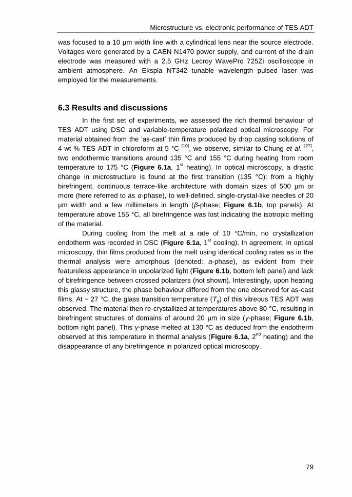
Microstructure vs. electronic performance of TES ADT
79
was focused to a 10 μm width line with a cylindrical lens near the source electrode.
Voltages were generated by a CAEN N1470 power supply, and current of the drain
electrode was measured with a 2.5 GHz Lecroy WavePro 725Zi oscilloscope in
ambient atmosphere. An Ekspla NT342 tunable wavelength pulsed laser was
employed for the measurements.
6.3 Results and discussions
In the first set of experiments, we assessed the rich thermal behaviour of
TES ADT using DSC and variable-temperature polarized optical microscopy. For
material obtained from the ‘as-cast’ thin films produced by drop casting solutions of
4 wt % TES ADT in chloroform at 5 °C [10]
, we observe, similar to Chung et al. [27]
,
two endothermic transitions around 135 °C and 155 °C during heating from room
temperature to 175 °C (Figure 6.1a, 1st heating). In optical microscopy, a drastic
change in microstructure is found at the first transition (135 °C): from a highly
birefringent, continuous terrace-like architecture with domain sizes of 500 μm or
more (here referred to as α-phase), to well-defined, single-crystal-like needles of 20
μm width and a few millimeters in length (β-phase; Figure 6.1b, top panels). At
temperature above 155 °C, all birefringence was lost indicating the isotropic melting
of the material.
During cooling from the melt at a rate of 10 °C/min, no crystallization
endotherm was recorded in DSC (Figure 6.1a, 1st cooling). In agreement, in optical
microscopy, thin films produced from the melt using identical cooling rates as in the
thermal analysis were amorphous (denoted: a-phase), as evident from their
featureless appearance in unpolarized light (Figure 6.1b, bottom left panel) and lack
of birefringence between crossed polarizers (not shown). Interestingly, upon heating
this glassy structure, the phase behaviour differed from the one observed for as-cast
films. At ~ 27 °C, the glass transition temperature (Tg) of this vitreous TES ADT was
observed. The material then re-crystallized at temperatures above 80 °C, resulting in
birefringent structures of domains of around 20 μm in size (γ-phase; Figure 6.1b,
bottom right panel). This γ-phase melted at 130 °C as deduced from the endotherm
observed at this temperature in thermal analysis (Figure 6.1a, 2nd
heating) and the
disappearance of any birefringence in polarized optical microscopy.
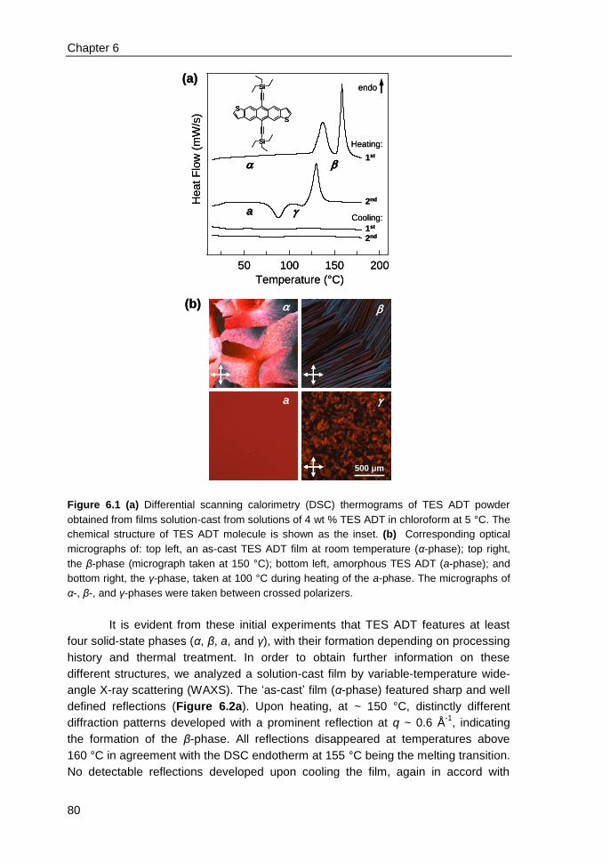
Chapter 6
80
50 100 150 200
1st
Heating:
Temperature (°C)
Heat F
low
(m
W/s
)
Cooling:
2nd
1st
2nd
endo
a
(a)
Si
Si
S
S
Si
Si
S
S
50 100 150 200
1st
Heating:
Temperature (°C)
Heat F
low
(m
W/s
)
Cooling:
2nd
1st
2nd
endo
a
(a)
Si
Si
S
S
Si
Si
S
S
500 μm
a
(b)
500 μm
a
(b)
Figure 6.1 (a) Differential scanning calorimetry (DSC) thermograms of TES ADT powder
obtained from films solution-cast from solutions of 4 wt % TES ADT in chloroform at 5 °C. The
chemical structure of TES ADT molecule is shown as the inset. (b) Corresponding optical
micrographs of: top left, an as-cast TES ADT film at room temperature (α-phase); top right,
the β-phase (micrograph taken at 150 °C); bottom left, amorphous TES ADT (a-phase); and
bottom right, the γ-phase, taken at 100 °C during heating of the a-phase. The micrographs of
α-, β-, and γ-phases were taken between crossed polarizers.
It is evident from these initial experiments that TES ADT features at least
four solid-state phases (α, β, a, and γ), with their formation depending on processing
history and thermal treatment. In order to obtain further information on these
different structures, we analyzed a solution-cast film by variable-temperature wide-
angle X-ray scattering (WAXS). The ‘as-cast’ film (α-phase) featured sharp and well
defined reflections (Figure 6.2a). Upon heating, at ~ 150 °C, distinctly different
diffraction patterns developed with a prominent reflection at q ~ 0.6 Å-1
, indicating
the formation of the β-phase. All reflections disappeared at temperatures above
160 °C in agreement with the DSC endotherm at 155 °C being the melting transition.
No detectable reflections developed upon cooling the film, again in accord with
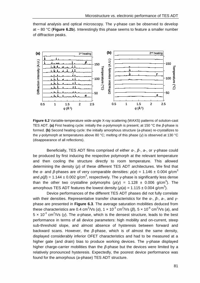
Microstructure vs. electronic performance of TES ADT
81
thermal analysis and optical microscopy. The γ-phase can be observed to develop
at ~ 80 °C (Figure 6.2b). Interestingly this phase seems to feature a smaller number
of diffraction peaks.
0.5 1 1.5 2
q (Å-1)
50
100
150 Tem
pera
ture
(°C)
2.5
Diffr
action inte
nsity (
A.U
.)
(a)
1st heating
0.5 1 1.5 2
q (Å-1)
50
100
150 Tem
pera
ture
(°C)
2.5
Diffr
action inte
nsity (
A.U
.)
(a)
1st heating
0.5 1 1.5 2
q (Å-1)
50
100
150 Tem
pera
ture
(°C)
2.5
Diffr
action inte
nsity (
A.U
.)
(b)
a
2nd heating
0.5 1 1.5 2
q (Å-1)
50
100
150 Tem
pera
ture
(°C)
2.5
Diffr
action inte
nsity (
A.U
.)
(b)
a
2nd heating
Figure 6.2 Variable-temperature wide-angle X-ray scattering (WAXS) patterns of solution-cast
TES ADT. (a) First heating cycle: initially the α-polymorph is present; at 150 °C the β-phase is
formed. (b) Second heating cycle: the initially amorphous structure (a-phase) re-crystallizes to
the γ-polymorph at temperatures above 80 °C; melting of this phase (γ) is observed at 130 °C
(disappearance of all reflections).
Beneficially, TES ADT films comprised of either α-, β-, a-, or γ-phase could
be produced by first inducing the respective polymorph at the relevant temperature
and then cooling the structure directly to room temperature. This allowed
determining the density (ρ) of these different TES ADT architectures. We find that
the α- and β-phases are of very comparable densities: ρ(α) = 1.146 ± 0.004 g/cm3
and ρ(β) = 1.144 ± 0.002 g/cm3, respectively. The γ-phase is significantly less dense
than the other two crystalline polymorphs (ρ(γ) = 1.128 ± 0.006 g/cm3). The
amorphous TES ADT features the lowest density (ρ(a) = 1.115 ± 0.004 g/cm3).
Device performances of the different TES ADT phases did not fully correlate
with their densities. Representative transfer characteristics for the α-, β-, a-, and γ-
phase are presented in Figure 6.3. The average saturation mobilities deduced from
these characteristics are 0.4 cm2/Vs (α), 1 × 10
-3 cm
2/Vs (β), 5 × 10
-6 cm
2/Vs (a), and
5 × 10⁻³
cm2/Vs (γ). The α-phase, which is the densest structure, leads to the best
performance in terms of all device parameters: high mobility and on-current, steep
sub-threshold slope, and almost absence of hysteresis between forward and
backward scans. However, the β-phase, which is of almost the same density,
displayed considerably inferior OFET characteristics and had to be measured at a
higher gate (and drain) bias to produce working devices. The γ-phase displayed
higher charge-carrier mobilities than the β-phase but the devices were limited by a
relatively pronounced hysteresis. Expectedly, the poorest device performance was
found for the amorphous (a-phase) TES ADT structure.
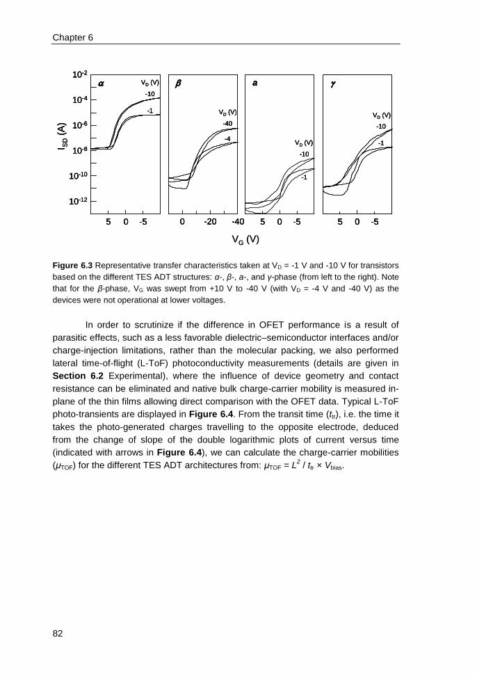
Chapter 6
82
VG (V)
-405 0 -5
10-2
I SD
(A)
10-8
10-10
10-12
10-4
10-6
0 -20
VD (V)
-10
-1
-40
-4
VD (V)
5 0 -5 5 0 -5
-10
-1
VD (V)
a
-10
-1
VD (V)
VG (V)
-405 0 -5
10-2
I SD
(A)
10-8
10-10
10-12
10-4
10-6
0 -20
VD (V)
-10
-1
-40
-4
VD (V)
-405 0 -5
10-2
I SD
(A)
10-8
10-10
10-12
10-4
10-6
0 -20
VD (V)
-10
-1
-40
-4
VD (V)
5 0 -5 5 0 -5
-10
-1
VD (V)
a
-10
-1
VD (V)
5 0 -5 5 0 -55 0 -5
-10
-1
VD (V)
a
-10
-1
VD (V)
Figure 6.3 Representative transfer characteristics taken at VD = -1 V and -10 V for transistors
based on the different TES ADT structures: α-, β-, a-, and γ-phase (from left to the right). Note
that for the β-phase, VG was swept from +10 V to -40 V (with VD = -4 V and -40 V) as the
devices were not operational at lower voltages.
In order to scrutinize if the difference in OFET performance is a result of
parasitic effects, such as a less favorable dielectric–semiconductor interfaces and/or
charge-injection limitations, rather than the molecular packing, we also performed
lateral time-of-flight (L-ToF) photoconductivity measurements (details are given in
Section 6.2 Experimental), where the influence of device geometry and contact
resistance can be eliminated and native bulk charge-carrier mobility is measured in-
plane of the thin films allowing direct comparison with the OFET data. Typical L-ToF
photo-transients are displayed in Figure 6.4. From the transit time (ttr), i.e. the time it
takes the photo-generated charges travelling to the opposite electrode, deduced
from the change of slope of the double logarithmic plots of current versus time
(indicated with arrows in Figure 6.4), we can calculate the charge-carrier mobilities
(μTOF) for the different TES ADT architectures from: μTOF = L2 / ttr × Vbias.
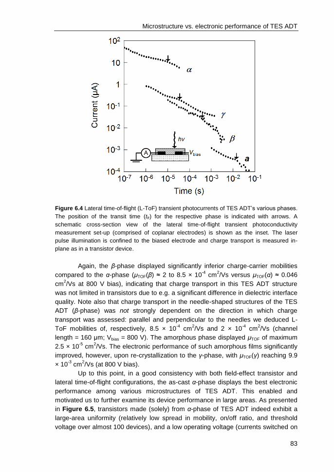
Microstructure vs. electronic performance of TES ADT
83
Figure 6.4 Lateral time-of-flight (L-ToF) transient photocurrents of TES ADT’s various phases.
The position of the transit time (ttr) for the respective phase is indicated with arrows. A
schematic cross-section view of the lateral time-of-flight transient photoconductivity
measurement set-up (comprised of coplanar electrodes) is shown as the inset. The laser
pulse illumination is confined to the biased electrode and charge transport is measured in-
plane as in a transistor device.
Again, the β-phase displayed significantly inferior charge-carrier mobilities
compared to the α-phase (μTOF(β) ≈ 2 to 8.5 × 10⁻⁴
cm2/Vs versus μTOF(α) ≈ 0.046
cm2/Vs at 800 V bias), indicating that charge transport in this TES ADT structure
was not limited in transistors due to e.g. a significant difference in dielectric interface
quality. Note also that charge transport in the needle-shaped structures of the TES
ADT (β-phase) was not strongly dependent on the direction in which charge
transport was assessed: parallel and perpendicular to the needles we deduced L-
ToF mobilities of, respectively, 8.5 × 10⁻⁴
cm2/Vs and 2 × 10
-4 cm
2/Vs (channel
length = 160 μm; Vbias = 800 V). The amorphous phase displayed μTOF of maximum
2.5 × 10⁻⁵
cm2/Vs. The electronic performance of such amorphous films significantly
improved, however, upon re-crystallization to the γ-phase, with μTOF(γ) reaching 9.9
× 10-3
cm2/Vs (at 800 V bias).
Up to this point, in a good consistency with both field-effect transistor and
lateral time-of-flight configurations, the as-cast α-phase displays the best electronic
performance among various microstructures of TES ADT. This enabled and
motivated us to further examine its device performance in large areas. As presented
in Figure 6.5, transistors made (solely) from α-phase of TES ADT indeed exhibit a
large-area uniformity (relatively low spread in mobility, on/off ratio, and threshold
voltage over almost 100 devices), and a low operating voltage (currents switched on
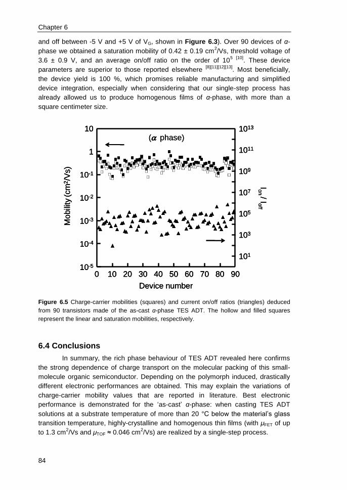
Chapter 6
84
and off between -5 V and +5 V of VG, shown in Figure 6.3). Over 90 devices of α-
phase we obtained a saturation mobility of 0.42 ± 0.19 cm2/Vs, threshold voltage of
3.6 ± 0.9 V, and an average on/off ratio on the order of 105
[10]. These device
parameters are superior to those reported elsewhere [8][11][12][13]
. Most beneficially,
the device yield is 100 %, which promises reliable manufacturing and simplified
device integration, especially when considering that our single-step process has
already allowed us to produce homogenous films of α-phase, with more than a
square centimeter size.
1
10-4
10-2
10-3
Device number
Mo
bili
ty(c
m2/V
s)
10-1
1011
101
109
105
103
107
Ion
/ Ioff
101310
0 10 20 30 40 50 60 70 908010-5
( phase)
1
10-4
10-2
10-3
Device number
Mo
bili
ty(c
m2/V
s)
10-1
1011
101
109
105
103
107
Ion
/ Ioff
101310
0 10 20 30 40 50 60 70 908010-5
1
10-4
10-2
10-3
Device number
Mo
bili
ty(c
m2/V
s)
10-1
1011
101
109
105
103
107
Ion
/ Ioff
101310
0 10 20 30 40 50 60 70 908010-5
( phase)
Figure 6.5 Charge-carrier mobilities (squares) and current on/off ratios (triangles) deduced
from 90 transistors made of the as-cast α-phase TES ADT. The hollow and filled squares
represent the linear and saturation mobilities, respectively.
6.4 Conclusions
In summary, the rich phase behaviour of TES ADT revealed here confirms
the strong dependence of charge transport on the molecular packing of this small-
molecule organic semiconductor. Depending on the polymorph induced, drastically
different electronic performances are obtained. This may explain the variations of
charge-carrier mobility values that are reported in literature. Best electronic
performance is demonstrated for the ‘as-cast’ α-phase: when casting TES ADT
solutions at a substrate temperature of more than 20 °C below the material’s glass
transition temperature, highly-crystalline and homogenous thin films (with μFET of up
to 1.3 cm2/Vs and μTOF ≈ 0.046 cm
2/Vs) are realized by a single-step process.
Microstructure vs. electronic performance of TES ADT
85
Meanwhile, a direct correlation of charge transport and solid-state density is
not found among different phases; thus an in-detail further study of the various
crystal structures that TES ADT can adopt should be envisioned, in order to obtain a
better understanding of relevant structure/processing/property/performance
interrelationships, from molecular level to macroscopic scale. Identification of the
best-performing (α-) phase is a first step towards such an understanding, and more
importantly, it already allowed us to fabricate high-performance bottom-gate/bottom-
contact transistors over large areas, as scrutinized based on more than 90 OFETs
made (solely) of α-phase, without formation of any low(er) mobility structures such
as the amorphous phase.
6.5 References
[1] A. Dodabalapur, Mater. Today 2006, 9, 24–30. [2] G. Gelinck, P. Heremans, K. Nomoto, T.D. Anthopoulos, Adv. Mater. 2010,
22, 3778–3798. [3] L. Zhang, C. Di, G. Yu, Y. Liu, J. Mater. Chem. 2010, 20, 7059–7073. [4] A. Mishra, P. Bäuerle, Angew. Chem. Int. Ed. 2012, 51, 2020–2067. [5] P.M. Beaujuge, J.M.J. Fréchet, J. Am. Chem. Soc. 2011, 133, 20009–20029. [6] L. Duan, L. Hou, T.-W. Lee, J. Qiao, D. Zhang, G. Dong, L. Wang, Y. Qiu, J.
Mater. Chem. 2010, 20, 6392–6407. [7] M. Cai, T. Xiao, E. Hellerich, Y. Chen, R. Shinar, J. Shinar, Adv. Mater. 2011,
23, 3590–3596. [8] M.M. Payne, S.R. Parkin, J.E. Anthony, C.C. Kuo, T.N. Jackson, J. Am.
Chem. Soc. 2005, 127, 4986–4987. [9] J. Anthony, Chem. Rev. 2006, 106, 5028–5048. [10] L. Yu, X. Li, E. Pavlica, M.A. Loth, J.E. Anthony, G. Bratina, C. Kjellander, G.
Gelinck, N. Stingelin, Appl. Phys. Lett. 2011, 99, 263304. [11] K.C. Dickey, J.E. Anthony, Y.-L. Loo, Adv. Mater. 2006, 18, 1721–1726. [12] W.H. Lee, J.A. Lim, D.H. Kim, J.H. Cho, Y. Jang, Y.H. Kim, J.I. Han, K. Cho,
Adv. Funct. Mater. 2008, 18, 560–565. [13] W.H. Lee, D.H. Kim, J.H. Cho, Y. Jang, J.A. Lim, D. Kwak, K. Cho, Appl.
Phys. Lett. 2007, 91, 092105. [14] J. Anthony, Angew. Chem. Int. Ed. 2008, 47, 452–483. [15] N. Karl, Synth. Met. 2003, 133-134, 649–657. [16] M. Shtein, J. Mapel, J.B. Benziger, S.R. Forrest, Appl. Phys. Lett. 2002, 81,
268–270. [17] D.J. Gundlach, J.E. Royer, S.K. Park, S. Subramanian, O.D. Jurchescu, B.H.
Hamadani, A.J. Moad, R.J. Kline, L.C. Teague, O. Kirillov, C.A. Richter, J.G. Kushmerick, L.J. Richter, S.R. Parkin, T.N. Jackson, J.E. Anthony, Nat. Mater. 2008, 7, 216–221.
[18] C.W. Sele, B.K.C. Kjellander, B. Niesen, M.J. Thornton, J.B.P.H. van der Putten, K. Myny, H.J. Wondergem, A. Moser, R. Resel, A.J.J.M. van Breemen, N. van Aerle, P. Heremans, J.E. Anthony, G.H. Gelinck, Adv. Mater. 2009, 21, 4926–4931.
[19] J. Rivnay, L.H. Jimison, J.E. Northrup, M.F. Toney, R. Noriega, S. Lu, T.J. Marks, A. Facchetti, A. Salleo, Nat. Mater. 2009, 8, 952–958.
[20] A. Salleo, R.J. Kline, D.M. DeLongchamp, M.L. Chabinyc, Adv. Mater. 2010, 22, 3812–3838.

Chapter 6
86
[21] I. McCulloch, M. Heeney, M.L. Chabinyc, D. DeLongchamp, R.J. Kline, M. Cölle, W. Duffy, D. Fischer, D. Gundlach, B. Hamadani, R. Hamilton, L. Richter, A. Salleo, M. Shkunov, D. Sparrowe, S. Tierney, W. Zhang, Adv. Mater. 2009, 21, 1091–1109.
[22] Y. Zhang, C. Kim, J. Lin, T. Nguyen, Adv. Funct. Mater. 2012, 22, 97–105. [23] M. Tantiwiwat, A. Tamayo, N. Luu, X.-D. Dang, T.-Q. Nguyen, J. Phys.
Chem. C 2008, 112, 17402–17407. [24] J.C. Conboy, E.J.C. Olson, D.M. Adams, J. Kerimo, A. Zaban, B.A. Gregg,
P.F. Barbara, J. Phys. Chem. B 1998, 102, 4516–4525. [25] A. Amassian, V. Pozdin, R. Li, D. Smilgies, G. Malliaras, J. Mater. Chem.
2010, 20, 2623–2629. [26] C. Liu, T. Minari, X. Lu, A. Kumatani, K. Takimiya, K. Tsukagoshi, Adv. Mater.
2011, 23, 523–526. [27] Y.S. Chung, N. Shin, J. Kang, Y. Jo, V.M. Prabhu, S.K. Satija, R.J. Kline,
D.M. DeLongchamp, M.F. Toney, M.A. Loth, B. Purushothaman, J.E. Anthony, D.Y. Yoon, J. Am. Chem. Soc. 2011, 133, 412–415.
[28] X. Li, B.K.C. Kjellander, J.E. Anthony, C.W.M. Bastiaansen, D.J. Broer, G.H. Gelinck, Adv. Funct. Mater. 2009, 19, 3610–3617.
[29] D. Kumaki, M. Yahiro, Y. Inoue, S. Tokito, Appl. Phys. Lett. 2007, 90, 133511.
[30] D. Janssen, R. De Palma, S. Verlaak, P. Heremans, W. Dehaen, Thin Solid Films 2006, 515, 1433–1438.
87
CHAPTER VII
7. n-type self-assembled monolayer
field-effect transistors: towards self-
assembled complementary organic
circuits
In this chapter we will present the first highly-reproducible n-type self-assembled
monolayer field-effect transistors (SAMFETs), based on a perylene derivative
(namely PBI-PA) with a phosphonic acid anchoring group which enables an efficient
fixation to aluminum oxide. Simple device fabrication under ambient conditions leads
to a complete surface coverage of the aluminum oxide with a monolayer of PBI-PA,
and to transistors with electron mobilities up to 10-3
cm2/Vs for channel length as
long as 100 μm. We will show that, despite the lack of long range in-plane order in
the monolayer, our PBI-PA SAMFETs still exhibit decent electron mobilities. Finally,
by implementing p- and n-type SAMFETs in one circuit, a complementary inverter
based solely on SAMFETs, with a large noise margin of 7 volts and a gain up to 15,
was demonstrated for the first time, paving the way to robust and low-power self-
assembled monolayer based complementary circuits.
To be published as:
A. Ringk, X. Li, F. Gholamrezaie, E. C. P. Smits, A. Neuhold, A. Moser, G. H.
Gelinck, R. Resel, D. M. de Leeuw, P. Strohriegl, 2012, submitted to Adv. Mater..

Chapter 7
88
7.1 Introduction
Self-assembled monolayers (SAMs) are dense organic layers
spontaneously formed on a surface [1]
. The autonomous and selective organization
of molecules without human intervention is a promising technology for mass
production of organic electronics. Self-assembled monolayer field-effect transistors
(SAMFETs) where the organic semiconductor consists of only one monolayer
covalently anchored onto the dielectric have been reported [2][3]
. The covalent fixation
of the active material to the dielectric allows the fabrication of flexible and
transparent devices [4]
with reduced delamination of the semiconductor during
bending. The absence of bulk material eliminates bulk currents to give high on/off
current ratios. A dense packing of the chromophores, full coverage, and strong π-π
coupling over long distances are required for reliable devices [5]
and enable a two
dimensional charge transport between the source and drain electrodes.
So far the most promising SAMFETs have been demonstrated using a
quinquethiophene derivative attached to silicon dioxide [6]
. Hole mobilities up to 10-2
cm2/Vs were achieved and the first unipolar integrated circuits as for example a 15-
bit code generator based on SAMFETs, were made. State of the art integrated
circuits however are mostly based on the well-established complementary metal
oxide semiconductor (CMOS) technique, where pairs of p- and n-type transistors are
combined in one device. This circuit design results in high noise immunity and low
power consumption. To realize complementary organic circuits based on self-
assembled monolayers, suitable n-type materials for the preparation of SAMFETs
are required. Compared to p-type materials it is difficult to find n-type transistor
materials, because of their high reactivity towards oxygen and moisture [7][8]
. Only
recently have stable n-type semiconducting materials been demonstrated with
mobilities matching those of p-type semiconductors [9][10]
.
Progress on fabricating n-type SAMFETs has been reported [11]
. A
semiconducting fullerene based monolayer (C60C18-PA) on aluminum oxide was
shown to exhibit electron mobilities up to 10-4
cm2/Vs. A major issue in this work is
that the C60C18-PA monolayers tend to form disordered layers with poor electrical
properties as a result. A possible suggested solution is to use mixed monolayers [12]
.
By the combination of C60C18-PA together with a C12 fluorinated phosphonic acid
the out of plane order in the SAMs could be improved. The result – a mixed
monolayer of both species – will however always be a necessary trade-off between
interfacial order and surface coverage [12]
. The lack of reliable n-type SAMFET
materials hampers the realization of self-assembled CMOS circuits. High
performance and reliable n-type SAMFETs will enable a huge step forward in a
bottom-up approach towards robust self-assembled complementary organic circuits.
Here we present highly reproducible n-type SAMFETs based on
heterosubstituted perylene bisimides with mobilities up to 10-3
cm2/Vs. By
implementing p- and n-type transistors, complementary inverters based solely on
SAMFETs with large noise margin of 7 volts and a gain up to 15 are demonstrated.
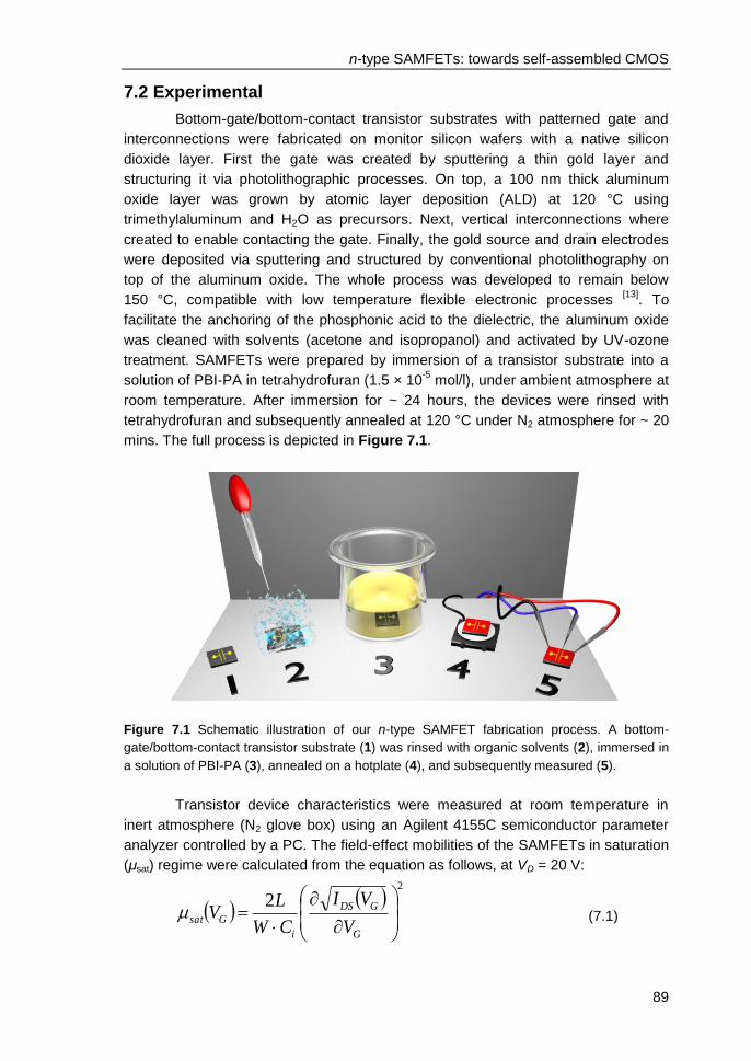
n-type SAMFETs: towards self-assembled CMOS
89
7.2 Experimental
Bottom-gate/bottom-contact transistor substrates with patterned gate and
interconnections were fabricated on monitor silicon wafers with a native silicon
dioxide layer. First the gate was created by sputtering a thin gold layer and
structuring it via photolithographic processes. On top, a 100 nm thick aluminum
oxide layer was grown by atomic layer deposition (ALD) at 120 °C using
trimethylaluminum and H2O as precursors. Next, vertical interconnections where
created to enable contacting the gate. Finally, the gold source and drain electrodes
were deposited via sputtering and structured by conventional photolithography on
top of the aluminum oxide. The whole process was developed to remain below
150 °C, compatible with low temperature flexible electronic processes [13]
. To
facilitate the anchoring of the phosphonic acid to the dielectric, the aluminum oxide
was cleaned with solvents (acetone and isopropanol) and activated by UV-ozone
treatment. SAMFETs were prepared by immersion of a transistor substrate into a
solution of PBI-PA in tetrahydrofuran (1.5 × 10⁻⁵
mol/l), under ambient atmosphere at
room temperature. After immersion for ~ 24 hours, the devices were rinsed with
tetrahydrofuran and subsequently annealed at 120 °C under N2 atmosphere for ~ 20
mins. The full process is depicted in Figure 7.1.
Figure 7.1 Schematic illustration of our n-type SAMFET fabrication process. A bottom-
gate/bottom-contact transistor substrate (1) was rinsed with organic solvents (2), immersed in
a solution of PBI-PA (3), annealed on a hotplate (4), and subsequently measured (5).
Transistor device characteristics were measured at room temperature in
inert atmosphere (N2 glove box) using an Agilent 4155C semiconductor parameter
analyzer controlled by a PC. The field-effect mobilities of the SAMFETs in saturation
(μsat) regime were calculated from the equation as follows, at VD = 20 V:
2
2
G
GDS
i
GsatV
VI
CW
LV
(7.1)
Chapter 7
90
where Ci is the capacitance per unit area of the gate dielectric layer (70 nF/cm2 for
the aluminum oxide used in this work), and L and W are channel length and width,
respectively. The threshold voltage (Vth) of the devices was extracted by
extrapolating the square root (SQRT) of |IDS,sat| vs. VG plot to IDS,sat = 0 (as depicted
by the dashed plot of Figure 7.4a).
7.3 Results and discussions
The perylene bisimide derivative N-(1-hexylheptyl)-N`-(undecyl-11-
phosphonic acid) perylene-3,4,9,10-tetracarboxylic bisimide, (PBI-PA), was
synthesized as the n-type active material in our SAMFETs. The molecule belongs to
a class of semiconductors well-known for their high performance in n-type organic
transistors [8]
. The chemical structure of PBI-PA is shown as the inset of Figure 7.2.
The active molecule PBI-PA consists of a heterosubstituted perylene bisimide core
bearing a branched alkyl tail to increase the solubility on one side, and a linear
undecyl alkyl chain with a phosphonic acid anchor group on the other side. The
phosphonic acid allows a covalent fixation of PBI-PA to aluminum oxide. Major
benefits of phosphonic acid terminated molecules compared to the chlorosilanes
previously reported [6]
are easier handling, storage and device fabrication as they are
environmentally stable.
Bottom-gate/bottom-contact PBI-PA SAMFETs were prepared by immersing
the transistor substrate with an aluminum oxide gate dielectric [13]
into a solution of
the PBI-PA molecule, under ambient atmosphere at room temperature (for details
see Section 7.2 Experimental). The high tendency to form aggregates in solution is
well known for perylene bisimides. However, the formation of large aggregates is
undesirable for depositing smooth and dense monolayers on surfaces.
Spectroscopic investigations revealed that at low concentrations of about 10-5
mol/l,
aggregation of perylenes is suppressed [14]
. During the immersion the phosphonic
acid reacts in a condensation reaction with the OH-groups on the oxide surface to
form a covalent bond [15]
. In comparison to thiols, which form relatively weak bonds
to gold, phosphonic acids bind more strongly to aluminum oxide [16]
.
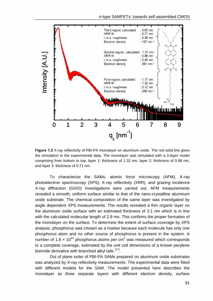
n-type SAMFETs: towards self-assembled CMOS
91
0 1 2 3 4 5 6 7 8 9
qz [nm
-1]
Inte
nsity [A
.U.]
0 1 2 3 4 5 6 7 8 9
qz [nm
-1]
Inte
nsity [A
.U.]
Figure 7.2 X-ray reflectivity of PBI-PA monolayer on aluminum oxide. The red solid line gives
the simulation to the experimental data. The monolayer was simulated with a 3-layer model
comprising from bottom to top, layer 1: thickness of 1.32 nm, layer 2: thickness of 0.98 nm,
and layer 3: thickness of 0.71 nm.
To characterize the SAMs, atomic force microscopy (AFM), X-ray
photoelectron spectroscopy (XPS), X-ray reflectivity (XRR), and grazing incidence
X-ray diffraction (GIXD) investigations were carried out. AFM measurements
revealed a smooth, uniform surface similar to that of the nano-crystalline aluminum
oxide substrate. The chemical composition of the same layer was investigated by
angle dependent XPS measurements. The results revealed a thin organic layer on
the aluminum oxide surface with an estimated thickness of 3.1 nm which is in line
with the calculated molecular length of 2.9 nm. This confirms the proper formation of
the monolayer on the surface. To determine the extent of surface coverage by XPS
analysis, phosphorus was chosen as a marker because each molecule has only one
phosphorus atom and no other source of phosphorus is present in the system. A
number of 1.8 × 10¹⁴
phosphorus atoms per cm2 was measured which corresponds
to a complete coverage, estimated by the unit cell dimensions of a known perylene
bisimide derivative with branched alkyl tails [17]
.
Out of plane order of PBI-PA SAMs prepared on aluminum oxide substrates
was analyzed by X-ray reflectivity measurements. The experimental data were fitted
with different models for the SAM. The model presented here describes the
monolayer as three separate layers with different electron density, surface
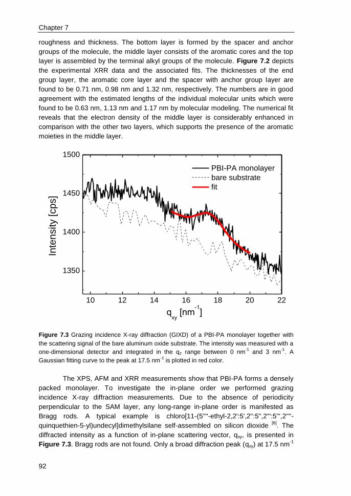
Chapter 7
92
roughness and thickness. The bottom layer is formed by the spacer and anchor
groups of the molecule, the middle layer consists of the aromatic cores and the top
layer is assembled by the terminal alkyl groups of the molecule. Figure 7.2 depicts
the experimental XRR data and the associated fits. The thicknesses of the end
group layer, the aromatic core layer and the spacer with anchor group layer are
found to be 0.71 nm, 0.98 nm and 1.32 nm, respectively. The numbers are in good
agreement with the estimated lengths of the individual molecular units which were
found to be 0.63 nm, 1.13 nm and 1.17 nm by molecular modeling. The numerical fit
reveals that the electron density of the middle layer is considerably enhanced in
comparison with the other two layers, which supports the presence of the aromatic
moieties in the middle layer.
10 12 14 16 18 20 22
1350
1400
1450
1500
qxy
[nm-1]
PBI-PA monolayer
bare substrate
fit
Inte
nsity [cps]
Figure 7.3 Grazing incidence X-ray diffraction (GIXD) of a PBI-PA monolayer together with
the scattering signal of the bare aluminum oxide substrate. The intensity was measured with a
one-dimensional detector and integrated in the qz range between 0 nm-1
and 3 nm-1
. A
Gaussian fitting curve to the peak at 17.5 nm-1
is plotted in red color.
The XPS, AFM and XRR measurements show that PBI-PA forms a densely
packed monolayer. To investigate the in-plane order we performed grazing
incidence X-ray diffraction measurements. Due to the absence of periodicity
perpendicular to the SAM layer, any long-range in-plane order is manifested as
Bragg rods. A typical example is chloro[11-(5''''-ethyl-2,2':5',2'':5'',2''':5''',2''''-
quinquethien-5-yl)undecyl]dimethylsilane self-assembled on silicon dioxide [6]
. The
diffracted intensity as a function of in-plane scattering vector, qxy, is presented in
Figure 7.3. Bragg rods are not found. Only a broad diffraction peak (qxy) at 17.5 nm-1
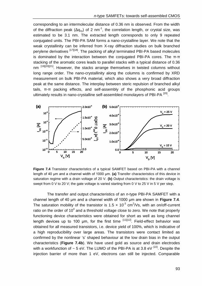
n-type SAMFETs: towards self-assembled CMOS
93
corresponding to an intermolecular distance of 0.36 nm is observed. From the width
of the diffraction peak (Δqxy) of 2 nm-1
, the correlation length, or crystal size, was
estimated to be 3.1 nm. The extracted length corresponds to only 9 repeated
conjugated units. The PBI-PA SAM forms a nano-crystalline layer. We note that the
weak crystallinity can be inferred from X-ray diffraction studies on bulk branched
perylene derivatives [17][18]
. The packing of alkyl terminated PBI-PA based molecules
is dominated by the interaction between the conjugated PBI-PA cores. The π-π
stacking of the aromatic cores leads to parallel stacks with a typical distance of 0.36
nm [19][20][21]
. However, the stacks arrange themselves in twisted columns without
long range order. The nano-crystallinity along the columns is confirmed by XRD
measurement on bulk PBI-PA material, which also shows a very broad diffraction
peak at the same distance. The interplay between steric repulsion of branched alkyl
tails, π-π packing effects, and self-assembly of the phosphonic acid groups
ultimately results in nano-crystalline self-assembled monolayers of PBI-PA [20]
.
0 5 10 15 2010
-12
10-11
10-10
10-9
10-8
VG [V]
I DS [A
]
0.0
5.0x10⁻⁵
1.0x10⁻⁴
1.5x10⁻⁴
2.0x10⁻⁴
SQ
RT
(IDS ) [A
1/2]
(a)
0 5 10 15 200.0
1.0x10⁻⁸
2.0x10⁻⁸
3.0x10⁻⁸
4.0x10⁻⁸
5.0x10⁻⁸
VG = 15 V
VG = 20 V
VG = 25 V
I DS [A
]
VD [V]
(b)
0 5 10 15 2010
-12
10-11
10-10
10-9
10-8
VG [V]
I DS [A
]
0.0
5.0x10⁻⁵
1.0x10⁻⁴
1.5x10⁻⁴
2.0x10⁻⁴
SQ
RT
(IDS ) [A
1/2]
(a)
0 5 10 15 2010
-12
10-11
10-10
10-9
10-8
VG [V]
I DS [A
]
0.0
5.0x10⁻⁵
1.0x10⁻⁴
1.5x10⁻⁴
2.0x10⁻⁴
SQ
RT
(IDS ) [A
1/2]
(a)
0 5 10 15 200.0
1.0x10⁻⁸
2.0x10⁻⁸
3.0x10⁻⁸
4.0x10⁻⁸
5.0x10⁻⁸
VG = 15 V
VG = 20 V
VG = 25 V
I DS [A
]
VD [V]
(b)
0 5 10 15 200.0
1.0x10⁻⁸
2.0x10⁻⁸
3.0x10⁻⁸
4.0x10⁻⁸
5.0x10⁻⁸
VG = 15 V
VG = 20 V
VG = 25 V
I DS [A
]
VD [V]
(b)
Figure 7.4 Transistor characteristics of a typical SAMFET based on PBI-PA with a channel
length of 40 μm and a channel width of 1000 μm. (a) Transfer characteristics of this device in
saturation regime with a drain voltage of 20 V. (b) Output characteristics: the drain voltage is
swept from 0 V to 20 V; the gate voltage is varied starting from 0 V to 25 V in 5 V per step.
The transfer and output characteristics of an n-type PBI-PA SAMFET with a
channel length of 40 μm and a channel width of 1000 μm are shown in Figure 7.4.
The saturation mobility of the transistor is 1.5 × 10⁻³
cm2/Vs, with an on/off-current
ratio on the order of 104 and a threshold voltage close to zero. We note that properly
functioning device characteristics were obtained for short as well as long channel
length devices up to 100 μm, for the first time [11][12]
. Field-effect behavior was
obtained for all measured transistors, i.e. device yield of 100%, which is indicative of
a high reproducibility over large areas. The transistors were contact limited as
confirmed by the nonlinear ‘s’ shaped behaviour at the low drain bias in the output
characteristics (Figure 7.4b). We have used gold as source and drain electrodes
with a workfunction of ~ 5 eV. The LUMO of the PBI-PA is at 3.8 eV [22]
. Despite the
injection barrier of more than 1 eV, electrons can still be injected. Comparable

Chapter 7
94
contact limited injection has been reported for thin-film transistors of semiconducting
PBI derivatives [23]
.
0 20 40 60 80 1000.0
5.0x10⁻⁴
1.0x10⁻³
1.5x10⁻³
2.0x10⁻³
S
atu
ratio
n M
ob
ility
[cm
2/V
s]
Channel Length [µm]
Figure 7.5 Scaling of mobility. The saturation mobility of PBI-PA SAMFETs as a function of
channel length (ranging from 2 to 100 μm). For channel lengths smaller than 40 μm the
mobility is dominated by the contact resistance. For larger channels the mobility becomes
independent of the channel length. The dashed line is a guide for the eye.
The saturation mobility as a function of channel length is presented in
Figure 7.5. In short channel transistors the transport is limited by the contact
resistance which lowers the mobility [24]
. For long channels the mobility is constant
up to a channel length of 100 μm. The constant mobility is remarkable. Traditionally,
as reported previously for p-type SAMFETs [5]
, the mobility of self-assembled
monolayer field-effect transistors decreases dramatically with increasing channel
length. This dependence is a direct consequence of incomplete coverage. Here the
mobility remains constant for channel lengths up to 100 μm, which is a fingerprint of
complete coverage with long-range connectivity within the SAM. The constant
mobility for long channel length, as shown in Figure 7.5, reflects the homogeneous
long-range charge transport through a densely packed monolayer without
conduction barriers from e.g. grain boundaries or from incomplete coverage. The
channel-length dependence of the carrier mobility (Figure 7.5), XPS investigations,
XRR, and XRD data confirm that a fully covered and conductive self-assembled
monolayer of PBI-PA was formed on the aluminum oxide surface.
A crucial step towards realizing robust and low power circuits is the use of
complementary logic. For SAMFET based complementary circuits reliable n-type as
well as p-type SAMFETs are essential. For this purpose p-type and n-type
SAMFETs were fabricated on two substrates and connected in a complementary
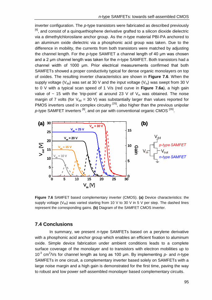
n-type SAMFETs: towards self-assembled CMOS
95
inverter configuration. The p-type transistors were fabricated as described previously [6]
, and consist of a quinquethiophene derivative grafted to a silicon dioxide dielectric
via a dimethylchlorosilane anchor group. As the n-type material PBI-PA anchored to
an aluminum oxide dielectric via a phosphonic acid group was taken. Due to the
difference in mobility, the currents from both transistors were matched by adjusting
the channel length. For the p-type SAMFET a channel length of 40 μm was chosen
and a 2 μm channel length was taken for the n-type SAMFET. Both transistors had a
channel width of 1000 μm. Prior electrical measurements confirmed that both
SAMFETs showed a proper conductivity typical for dense organic monolayers on top
of oxides. The resulting inverter characteristics are shown in Figure 7.6. When the
supply voltage (Vdd) was set at 30 V and the input voltage (Vin) was swept from 30 V
to 0 V with a typical scan speed of 1 V/s (red curve in Figure 7.6a), a high gain
value of ~ 15 with the ‘trip-point’ at around 23 V of Vin was obtained. The noise
margin of 7 volts (for Vdd = 30 V) was substantially larger than values reported for
PMOS inverters used in complex circuitry [25]
, also higher than the previous unipolar
p-type SAMFET inverters [6]
, and on par with conventional organic CMOS [26]
.
0 5 10 15 20 25 300
5
10
15
20
25
30
Vo
ut [
V]
Vin [V]
0
5
10
15
Vdd
= 10 V
Vdd
= 15 V
Vdd
= 20 V
Vdd
= 30 VV
dd = 25 V
Gain
(a) (b)
0 5 10 15 20 25 300
5
10
15
20
25
30
Vo
ut [
V]
Vin [V]
0
5
10
15
Vdd
= 10 V
Vdd
= 15 V
Vdd
= 20 V
Vdd
= 30 VV
dd = 25 V
Gain
(a)
0 5 10 15 20 25 300
5
10
15
20
25
30
Vo
ut [
V]
Vin [V]
0
5
10
15
Vdd
= 10 V
Vdd
= 15 V
Vdd
= 20 V
Vdd
= 30 VV
dd = 25 V
Gain
(a) (b)(b)
Figure 7.6 SAMFET based complementary inverter (CMOS). (a) Device characteristics: the
supply voltage (Vdd) was varied starting from 10 V to 30 V in 5 V per step. The dashed lines
represent the corresponding gains. (b) Diagram of the SAMFET CMOS inverter.
7.4 Conclusions
In summary, we present n-type SAMFETs based on a perylene derivative
with a phosphonic acid anchor group which enables an efficient fixation to aluminum
oxide. Simple device fabrication under ambient conditions leads to a complete
surface coverage of the monolayer and to transistors with electron mobilities up to
10-3
cm2/Vs for channel length as long as 100 μm. By implementing p- and n-type
SAMFETs in one circuit, a complementary inverter based solely on SAMFETs with a
large noise margin and a high gain is demonstrated for the first time, paving the way
to robust and low power self-assembled monolayer based complementary circuits.
Chapter 7
96
7.5 References
[1] G.M. Whitesides, B. Grzybowski, Science 2002, 295, 2418–2421. [2] G.S. Tulevski, Q. Miao, M. Fukuto, R. Abram, B. Ocko, R. Pindak, M.L.
Steigerwald, C.R. Kagan, C. Nuckolls, J. Am. Chem. Soc. 2004, 126, 15048–15050.
[3] D.O. Hutchins, O. Acton, T. Weidner, N. Cernetic, J.E. Baio, G. Ting, D.G. Castner, H. Ma, A.K.-Y. Jen, Org. Electron. 2012, 13, 464–468.
[4] F. Gholamrezaie, S.G.J. Mathijssen, E.C.P. Smits, T.C.T. Geuns, P.A. van Hal, S.A. Ponomarenko, H.-G. Flesch, R. Resel, E. Cantatore, P.W.M. Blom, D.M. de Leeuw, Nano Lett. 2010, 10, 1998–2002.
[5] S.G.J. Mathijssen, E.C.P. Smits, P.A. van Hal, H.J. Wondergem, S.A. Ponomarenko, A. Moser, R. Resel, P.A. Bobbert, M. Kemerink, R.A.J. Janssen, D.M. de Leeuw, Nat. Nano. 2009, 4, 674–680.
[6] E.C.P. Smits, S.G.J. Mathijssen, P.A. van Hal, S. Setayesh, T.C.T. Geuns, K.A.H.A. Mutsaers, E. Cantatore, H.J. Wondergem, O. Werzer, R. Resel, M. Kemerink, S. Kirchmeyer, A.M. Muzafarov, S.A. Ponomarenko, B. de Boer, P.W.M. Blom, D.M. de Leeuw, Nature 2008, 455, 956–959.
[7] D.M. de Leeuw, M.M.J. Simenon, A.R. Brown, R.E.F. Einerhand, Synth. Met. 1997, 87, 53–59.
[8] B.A. Jones, A. Facchetti, M.R. Wasielewski, T.J. Marks, J. Am. Chem. Soc. 2007, 129, 15259–15278.
[9] H. Yan, Z. Chen, Y. Zheng, C. Newman, J.R. Quinn, F. Dotz, M. Kastler, A. Facchetti, Nature 2009, 457, 679–686.
[10] J. Soeda, T. Uemura, Y. Mizuno, A. Nakao, Y. Nakazawa, A. Facchetti, J. Takeya, Adv. Mater. 2011, 23, 3681–3685.
[11] M. Novak, A. Ebel, T. Meyer-Friedrichsen, A. Jedaa, B.F. Vieweg, G. Yang, K. Voitchovsky, F. Stellacci, E. Spiecker, A. Hirsch, M. Halik, Nano Lett. 2011, 11, 156–159.
[12] A. Rumpel, M. Novak, J. Walter, B. Braunschweig, M. Halik, W. Peukert, Langmuir 2011, 27, 15016–15023.
[13] A.K. Tripathi, E.C.P. Smits, J.B.P.H. van der Putten, M. van Neer, K. Myny, M. Nag, S. Steudel, P. Vicca, K. O’Neill, E. van Veenendaal, J. Genoe, P. Heremans, G.H. Gelinck, Appl. Phys. Lett. 2011, 98, 162102.
[14] Z. Chen, V. Stepanenko, V. Dehm, P. Prins, L.D.A. Siebbeles, J. Seibt, P. Marquetand, V. Engel, F. Würthner, Chem. Eur. J 2007, 13, 436–449.
[15] P. Thissen, M. Valtiner, G. Grundmeier, Langmuir 2010, 26, 156–164. [16] I. Levine, S.M. Weber, Y. Feldman, T. Bendikov, H. Cohen, D. Cahen, A.
Vilan, Langmuir 2012, 28, 404–415. [17] V. Marcon, D.W. Breiby, W. Pisula, J. Dahl, J. Kirkpatrick, S. Patwardhan, F.
Grozema, D. Andrienko, J. Am. Chem. Soc. 2009, 131, 11426–11432. [18] F. Nolde, W. Pisula, S. Müller, C. Kohl, K. Müllen, Chem. Mater. 2006, 18,
3715–3725. [19] G. Klebe, F. Graser, E. Hädicke, J. Berndt, Acta Crystallogr., Sect. B: Struct.
Sci. 1989, B45, 69–77. [20] M.R. Hansen, R. Graf, S. Sekharan, D. Sebastiani, J. Am. Chem. Soc. 2009,
131, 5251–5256. [21] O. Guillermet, M. Mossoyan-Déneux, M. Giorgi, A. Glachant, J.C. Mossoyan,
Thin Solid Films 2006, 514, 25–32.
n-type SAMFETs: towards self-assembled CMOS
97
[22] A. Wicklein, A. Lang, M. Muth, M. Thelakkat, J. Am. Chem. Soc. 2009, 131, 14442–14453.
[23] S. Fabiano, H. Wang, C. Piliego, C. Jaye, D.A. Fischer, Z. Chen, B. Pignataro, A. Facchetti, Y. Loo, M.A. Loi, Adv. Funct. Mater. 2011, 21, 4479–4486.
[24] E. Meijer, G. Gelinck, E. van Veenendaal, B. Huisman, D. de Leeuw, T. Klapwijk, Appl. Phys. Lett. 2003, 82, 4576–4578.
[25] M. Spijkman, E.C.P. Smits, P.W.M. Blom, D.M. de Leeuw, Y. Bon Saint Côme, S. Setayesh, E. Cantatore, Appl. Phys. Lett. 2008, 92, 143304.
[26] G. Gelinck, P. Heremans, K. Nomoto, T.D. Anthopoulos, Adv. Mater. 2010, 22, 3778–3798.
98
CHAPTER VIII
8. Programmable polymer light
emitting transistors with ferroelectric
polarization-enhanced channel
current and light emission
In this last chapter, we will introduce an unconventional use of the molecular
(polymer chain/dipole) alignment, in the dielectric layer of organic field-effect
transistors. Here we present a voltage-programmable light-emitting field-effect
transistor (LEFET), consisting of a green emitting polymer (F8BT), and a
ferroelectric polymer, P(VDF-TrFE), as the gate dielectric. We show by both
experimental observations and numerical modeling that, when the ferroelectric gate
dielectric is polarized in opposite directions at the drain and source sides of the
channel, respectively, both electron and hole currents are enhanced, resulting in
more charge recombination and ~ 10 times higher light emission in a ferroelectric
LEFET, compared to the device with non-ferroelectric gate. As a result of the
ferroelectric poling (dipole alignment), our ferroelectric LEFETs exhibit repeated
programmability in light emission, and an external quantum efficiency (EQE) of up to
1.06 %. Numerical modeling reveals that the remnant polarization charge of the
ferroelectric layer tends to ‘pin’ the position of the recombination zone, paving the
way to integrate specific optical out-coupling structures in the channel of these
devices to further increase the brightness.
Published as:
X. Li, A. J. J. M. van Breemen, V. Khikhlovskyi, E. C. P. Smits, M. Kemerink, D. J.
Broer, G. H. Gelinck, Org. Electron. 2012, 13, 1742–1749.
Ferroelectric light emitting transistors
99
8.1 Introduction
Soluble polymer semiconductors have seen a large research and
development effort in the past ten years as they can be processed at ambient
temperature, starting from soluble, ink-like materials. The recent realization of
ambipolar currents in polymer field-effect transistors [1]
has enabled the fabrication of
polymer light emitting field-effect transistors (LEFETs) [2][3][4]
. The higher current
densities [5]
in these devices compared to those in diode-type devices may help to
reach population inversion which is a prerequisite for an electrically driven organic
laser. Apart from the possible use in an organic lasing device, LEFETs may be used
for low-loss light signal transmission in optoelectronic integrated circuits. The light
output of the LEFETs is yet too low for many practical applications. Several
approaches have been proposed to increase the light output by using for instance
bilayer structures composed of p-type and n-type semiconductors [6][7][8][9]
, organic
heterostructures in the channel [10][11]
, improved injection of both carriers by tuning
the work functions of injecting contacts [3][12]
, adding small amounts of
semiconducting carbon nanotubes [13]
, incorporating optical structures [14][15]
and
multiple gates [16]
. The drawback of these methods is that they add complexity to the
fabrication process.
In this work, we present a new strategy to improve the LEFET performance
using a ferroelectric polymer as the gate dielectric. When the ferroelectric gate
dielectric is polarized in opposite directions at the drain and source sides of the
channel, both electron and hole currents are enhanced, resulting in more charge
recombination and higher light emission. We show by both numerical modeling and
experimental results that channel current as well as light-emission efficiency is
increased in a ferroelectric LEFET compared to the device with non-ferroelectric
gate dielectric.
8.2 Experimental
Transistors in this study were prepared on a thick thermally grown layer of
SiO2 on top of a silicon support wafer. First, source and drain electrodes were made
by lithographically patterning a 30 nm-thick gold layer. A 1-propanethiol monolayer
was deposited on Au source-drain electrodes to improve the electron injection [12]
.
Then, a 70 nm-thick polyfluorene derivative, poly(9,9-di-n-octylfluorene-alt-
benzothiadiazole), F8BT (purchased from Sigma Aldrich and used as received), was
spincoated from anhydrous o-xylene (Sigma Aldrich) solution under N2 and
subsequently annealed at 120 °C on a hotplate to achieve a balanced optical gain
and charge transport for F8BT [12]
.
On top of F8BT, a ferroelectric polymer layer of poly(vinylidene fluoride-
trifluoroethylene), P(VDF-TrFE) (ratio 77/23, w/w%), provided by Solvay Specialty
Polymers, was spincoated under N2 from anhydrous butyl acetate (Sigma Aldrich)
solution with a thickness of 450 nm. The devices were annealed at 135 °C on a
hotplate for 1 hour under N2 to increase the crystallinity of the P(VDF-TrFE) film
Chapter 8
100
[17][18]. For comparative purposes we also made transistors with two other fluorinated
polymers as the dielectric layer: a 450 nm-thick polytrifluorethylene (PTrFE, from
Solvay Specialty Polymers) and a 200 nm-thick AF2400 (from DuPontTM
Teflon®,
FC-75 as its solvent). Finally, as semi-transparent top gate, a 20 nm-thick gold
electrode was evaporated in vacuum through a shadow mask. All transistors have a
channel length and width of 5 μm and 10 mm, respectively.
Opto-electrical characterizations were performed in a dark and N2-filled
glove-box (water and oxygen content below 0.1 ppm) at room temperature using an
Agilent 4155C semiconductor parameter analyser. The sweeping speed for I-V
scans was 1 V/s. Simultaneously, the light emission was measured by aligning a Si
photodiode (Hamamatsu S2386-18K, photo-sensitivity = 0.3 A/W at wavelength of
500 nm) just above the surface of the emission area at a vertical height (H) of 3.5
mm. The dimensions (0.2 mm by 0.5 mm) of the emission area were smaller than
the radius (r) of 0.55 mm of the active area of the photodiode. Assuming the angular
dependence of the light emission from our devices is close to that of a Lambertian
source [19][20][21][22][23][24]
, and the detection angle in our measurement geometry, θ =
arc tan (r / H), is small enough to justify a small-angle approximation [25]
, i.e. tan (θ) ≈
θ and cos (θ) ≈ 1 - θ2/2, we can estimate the total photocurrent (Ip-tot) from the
measured photocurrent (Ip) by using the following relation: Ip-tot = (H / r)2 × Ip. Finally
the external quantum efficiency (EQE) was calculated from the total photocurrent (Ip-
tot) by using similar methods as previously reported [11]
, which in our case can be
simplified to: EQE ≈ 62.27 × (Ip / ID). The calculated EQE values for the two
transistors presented in Figure 8.3 below reach 0.45 % and 0.16 % for the P(VDF-
TrFE) and PTrFE device, respectively (shown as insets of Figure 8.3b and d). The
EL spectra were recorded with an AvaSpec Avantes Fiber Optic spectrometer.
8.3 Opto-electrical characterizations & operation mechanism of
ferroelectric LEFETs
The chemical structures of the materials used, together with the schematic
layout of the LEFET, are shown in Figure 8.1 (detailed device preparations are
described in Section 8.2 Experimental). Source, drain and gate electrodes are
made of gold. A polyfluorene derivative, poly(9,9-di-n-octylfluorene-alt-
benzothiadiazole) (F8BT), was used as the semiconductor. F8BT is a well-studied
material in combination with LEFETs because of its high light emission in the visible
range and the fact that ambipolar currents can be attained in this material from gold
as the injecting contacts [4][26][27][28]
. A random copolymer of poly(vinylidene fluoride-
trifluoroethylene), P(VDF-TrFE) (ratio 77/23, w/w%), was used as the ferroelectric
gate dielectric, with a layer thickness of ~ 450 nm. The ferroelectric layer, because
of its remnant polarization, can adopt either of two stable remnant polarization states.
Switching from one polarization state to the other occurs by applying a sufficiently
large electric voltage over the ferroelectric layer, in our case ~ 30V [29]
. When the
polarization of the ferroelectric gate dielectric is oriented towards the gate electrode,
positive counter charges (holes) are induced in the semiconductor at the

Ferroelectric light emitting transistors
101
semiconductor/ferroelectric interface, i.e. the transistor channel. As a result, the
onset of hole accumulation in a p-type semiconductor shifts to a more positive gate
bias. Similarly, the opposite polarization state of the gate dielectric shifts the onset
voltage of electron accumulation to a more negative gate voltage. When the
polarization is oriented towards the gate electrode at the source side of the channel
and in the opposite direction at the drain side, it should be possible to accumulate
more holes at the source and simultaneously more electrons at the drain side of the
channel, respectively. This is illustrated schematically in Figure 8.1b.
F8BT P(VDF-TrFE)
(a)
(b)
Semiconductor
Substrate
Drain
Gate (Programmed)
Source
F8BT P(VDF-TrFE)
(a)
(b)
Semiconductor
Substrate
Drain
Gate (Programmed)
Source
Figure 8.1 (a) Chemical structures of the materials used: F8BT and P(VDF-TrFE). (b) Device
layout of the LEFET, with a schematic illustration of the ferroelectric-induced higher electron
and hole densities in the transistor channel, upon the programmed gate-voltage. More light
output is therefore expected from the ferroelectric LEFET compared with a conventional
LEFET.
Typical bistable transfer characteristics are presented in Figure 8.2a. The
simultaneously measured light emission (photocurrent Ip) is shown in Figure 8.2b.
The source electrode was grounded (VS = 0 V) and the gate bias (VG) was swept
from +60 V to -60 V and back to +60 V, while VD was kept at -60 V. Arrows indicate
the direction of the hysteresis. Because of the large VD, the electric field over the
ferroelectric dielectric is strongly dependent on the position in the channel. For all
gate voltages, the drain current exceeds the associated gate current. This means
that the drain current is predominantly due to charge transport in the semiconductor
channel. Relatively low drain currents are observed at positive gate bias compared
to the currents observed at negative gate bias. This indicates that the electron
mobility is much lower than the hole mobility. We estimate electron and hole
mobilities of 10-5
cm2/Vs and 10
-3 cm
2/Vs, respectively. Below we will come back to
the possible origin of the low electron mobility.
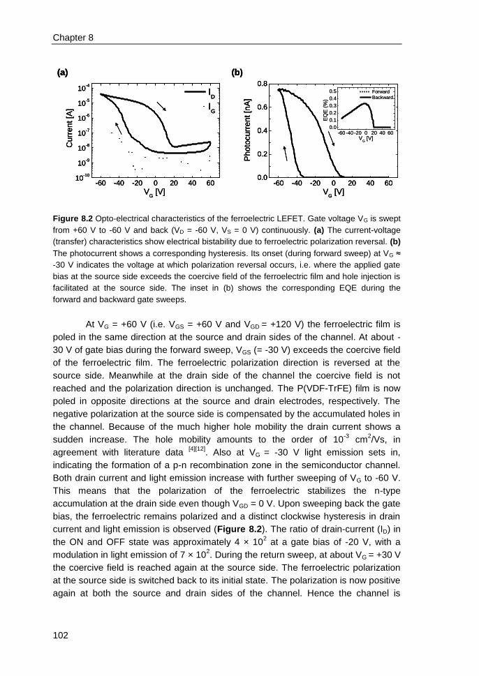
Chapter 8
102
-60 -40 -20 0 20 40 6010
-10
10-9
10-8
10-7
10-6
10-5
10-4
ID
IG
Curr
ent [A
]
VG [V]
hp04i02_Vg60to-60V_DOUBLE with Iph_Vd-60V_Id vs Ig_ABS
-60 -40 -20 0 20 40 600.0
0.2
0.4
0.6
0.8
Photo
curr
ent [n
A]
VG [V]
(a) (b)
-60 -40 -20 0 20 40 600.0
0.1
0.2
0.3
0.4
0.5
EQ
E (
%)
VG [V]
Forward
Backward
-60 -40 -20 0 20 40 6010
-10
10-9
10-8
10-7
10-6
10-5
10-4
ID
IG
Curr
ent [A
]
VG [V]
hp04i02_Vg60to-60V_DOUBLE with Iph_Vd-60V_Id vs Ig_ABS
-60 -40 -20 0 20 40 600.0
0.2
0.4
0.6
0.8
Photo
curr
ent [n
A]
VG [V]
(a) (b)
-60 -40 -20 0 20 40 6010
-10
10-9
10-8
10-7
10-6
10-5
10-4
ID
IG
Curr
ent [A
]
VG [V]
hp04i02_Vg60to-60V_DOUBLE with Iph_Vd-60V_Id vs Ig_ABS
-60 -40 -20 0 20 40 600.0
0.2
0.4
0.6
0.8
Photo
curr
ent [n
A]
VG [V]
(a) (b)
-60 -40 -20 0 20 40 600.0
0.1
0.2
0.3
0.4
0.5
EQ
E (
%)
VG [V]
Forward
Backward
Figure 8.2 Opto-electrical characteristics of the ferroelectric LEFET. Gate voltage VG is swept
from +60 V to -60 V and back (VD = -60 V, VS = 0 V) continuously. (a) The current-voltage
(transfer) characteristics show electrical bistability due to ferroelectric polarization reversal. (b)
The photocurrent shows a corresponding hysteresis. Its onset (during forward sweep) at VG ≈
-30 V indicates the voltage at which polarization reversal occurs, i.e. where the applied gate
bias at the source side exceeds the coercive field of the ferroelectric film and hole injection is
facilitated at the source side. The inset in (b) shows the corresponding EQE during the
forward and backward gate sweeps.
At VG = +60 V (i.e. VGS = +60 V and VGD = +120 V) the ferroelectric film is
poled in the same direction at the source and drain sides of the channel. At about -
30 V of gate bias during the forward sweep, VGS (= -30 V) exceeds the coercive field
of the ferroelectric film. The ferroelectric polarization direction is reversed at the
source side. Meanwhile at the drain side of the channel the coercive field is not
reached and the polarization direction is unchanged. The P(VDF-TrFE) film is now
poled in opposite directions at the source and drain electrodes, respectively. The
negative polarization at the source side is compensated by the accumulated holes in
the channel. Because of the much higher hole mobility the drain current shows a
sudden increase. The hole mobility amounts to the order of 10-3
cm2/Vs, in
agreement with literature data [4][12]
. Also at VG = -30 V light emission sets in,
indicating the formation of a p-n recombination zone in the semiconductor channel.
Both drain current and light emission increase with further sweeping of VG to -60 V.
This means that the polarization of the ferroelectric stabilizes the n-type
accumulation at the drain side even though VGD = 0 V. Upon sweeping back the gate
bias, the ferroelectric remains polarized and a distinct clockwise hysteresis in drain
current and light emission is observed (Figure 8.2). The ratio of drain-current (ID) in
the ON and OFF state was approximately 4 × 10² at a gate bias of -20 V, with a
modulation in light emission of 7 × 10². During the return sweep, at about VG = +30 V
the coercive field is reached again at the source side. The ferroelectric polarization
at the source side is switched back to its initial state. The polarization is now positive
again at both the source and drain sides of the channel. Hence the channel is
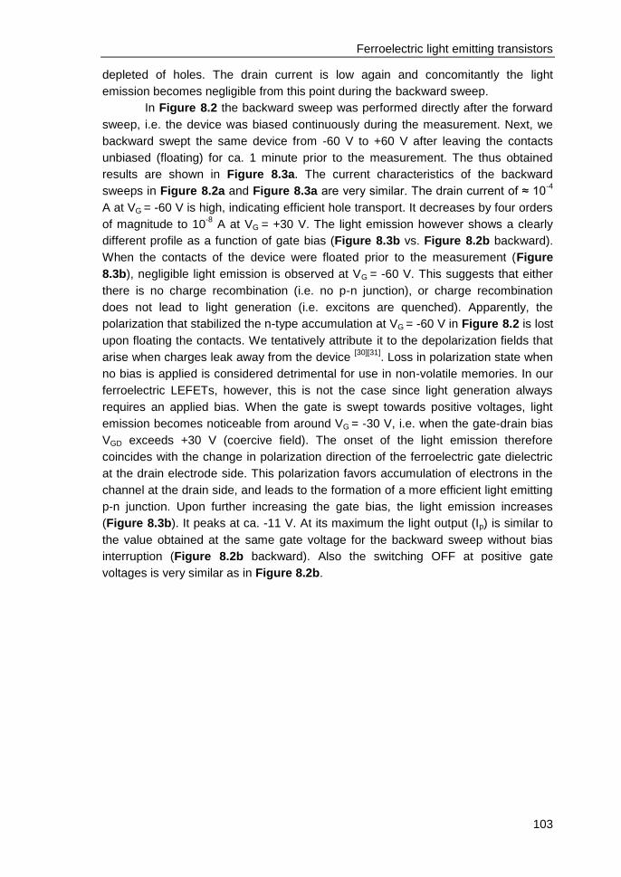
Ferroelectric light emitting transistors
103
depleted of holes. The drain current is low again and concomitantly the light
emission becomes negligible from this point during the backward sweep.
In Figure 8.2 the backward sweep was performed directly after the forward
sweep, i.e. the device was biased continuously during the measurement. Next, we
backward swept the same device from -60 V to +60 V after leaving the contacts
unbiased (floating) for ca. 1 minute prior to the measurement. The thus obtained
results are shown in Figure 8.3a. The current characteristics of the backward
sweeps in Figure 8.2a and Figure 8.3a are very similar. The drain current of ≈ 10-4
A at VG = -60 V is high, indicating efficient hole transport. It decreases by four orders
of magnitude to 10-8
A at VG = +30 V. The light emission however shows a clearly
different profile as a function of gate bias (Figure 8.3b vs. Figure 8.2b backward).
When the contacts of the device were floated prior to the measurement (Figure
8.3b), negligible light emission is observed at VG = -60 V. This suggests that either
there is no charge recombination (i.e. no p-n junction), or charge recombination
does not lead to light generation (i.e. excitons are quenched). Apparently, the
polarization that stabilized the n-type accumulation at VG = -60 V in Figure 8.2 is lost
upon floating the contacts. We tentatively attribute it to the depolarization fields that
arise when charges leak away from the device [30][31]
. Loss in polarization state when
no bias is applied is considered detrimental for use in non-volatile memories. In our
ferroelectric LEFETs, however, this is not the case since light generation always
requires an applied bias. When the gate is swept towards positive voltages, light
emission becomes noticeable from around VG = -30 V, i.e. when the gate-drain bias
VGD exceeds +30 V (coercive field). The onset of the light emission therefore
coincides with the change in polarization direction of the ferroelectric gate dielectric
at the drain electrode side. This polarization favors accumulation of electrons in the
channel at the drain side, and leads to the formation of a more efficient light emitting
p-n junction. Upon further increasing the gate bias, the light emission increases
(Figure 8.3b). It peaks at ca. -11 V. At its maximum the light output (Ip) is similar to
the value obtained at the same gate voltage for the backward sweep without bias
interruption (Figure 8.2b backward). Also the switching OFF at positive gate
voltages is very similar as in Figure 8.2b.
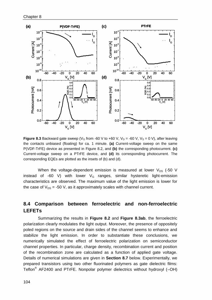
Chapter 8
104
-60 -40 -20 0 20 40 600.0
0.2
0.4
0.6
0.8
Pho
tocu
rre
nt
[nA
]
VG [V]
-60 -40 -20 0 20 40 600.0
0.2
0.4
0.6
0.8
Pho
tocu
rre
nt
[nA
]
VG [V]
-60 -40 -20 0 20 40 6010
-10
10-9
10-8
10-7
10-6
10-5
10-4
Curr
ent [A
]
VG [V]
ID
IG
HP02I02_Vg-60to60V_1way with Iph_Vd-60V_Id vs Ig_ABS
-60 -40 -20 0 20 40 6010
-10
10-9
10-8
10-7
10-6
10-5
10-4
Curr
ent [A
]
VG [V]
ID
IG
hp04i02_Vg-60to60V_1way with Iph_Vd-60V_Id vs Ig_ABS PTrFEP(VDF-TrFE)(a) (c)
(b) (d)
-60 -40 -20 0 20 40 600.0
0.1
0.2
0.3
0.4
0.5
EQ
E (
%)
VG [V]
-60 -40 -20 0 20 40 600.0
0.1
0.2
0.3
0.4
0.5
EQ
E (
%)
VG [V]
-60 -40 -20 0 20 40 600.0
0.2
0.4
0.6
0.8
Pho
tocu
rre
nt
[nA
]
VG [V]
-60 -40 -20 0 20 40 600.0
0.2
0.4
0.6
0.8
Pho
tocu
rre
nt
[nA
]
VG [V]
-60 -40 -20 0 20 40 6010
-10
10-9
10-8
10-7
10-6
10-5
10-4
Curr
ent [A
]
VG [V]
ID
IG
HP02I02_Vg-60to60V_1way with Iph_Vd-60V_Id vs Ig_ABS
-60 -40 -20 0 20 40 6010
-10
10-9
10-8
10-7
10-6
10-5
10-4
Curr
ent [A
]
VG [V]
ID
IG
hp04i02_Vg-60to60V_1way with Iph_Vd-60V_Id vs Ig_ABS PTrFEP(VDF-TrFE)(a) (c)
(b) (d)
-60 -40 -20 0 20 40 600.0
0.1
0.2
0.3
0.4
0.5
EQ
E (
%)
VG [V]
-60 -40 -20 0 20 40 600.0
0.1
0.2
0.3
0.4
0.5
EQ
E (
%)
VG [V]
Figure 8.3 Backward gate sweep (VG from -60 V to +60 V, VD = -60 V, VS = 0 V), after leaving
the contacts unbiased (floating) for ca. 1 minute. (a) Current-voltage sweep on the same
P(VDF-TrFE) device as presented in Figure 8.2, and (b) the corresponding photocurrent. (c)
Current-voltage sweep on a PTrFE device, and (d) its corresponding photocurrent. The
corresponding EQEs are plotted as the insets of (b) and (d).
When the voltage-dependent emission is measured at lower VDS (-50 V
instead of -60 V) with lower VG ranges, similar hysteretic light-emission
characteristics are observed. The maximum value of the light emission is lower for
the case of VDS = -50 V, as it approximately scales with channel current.
8.4 Comparison between ferroelectric and non-ferroelectric
LEFETs
Summarizing the results in Figure 8.2 and Figure 8.3ab, the ferroelectric
polarization clearly modulates the light output. Moreover, the presence of oppositely
poled regions on the source and drain sides of the channel seems to enhance and
stabilize the light emission. In order to substantiate these conclusions, we
numerically simulated the effect of ferroelectric polarization on semiconductor
channel properties. In particular, charge density, recombination current and position
of the recombination zone are calculated as a function of applied gate voltage.
Details of numerical simulations are given in Section 8.7 below. Experimentally, we
prepared transistors using two other fluorinated polymers as gate dielectric films:
Teflon® AF2400 and PTrFE. Nonpolar polymer dielectrics without hydroxyl (–OH)
Ferroelectric light emitting transistors
105
groups were frequently used in combination with organic semiconductors as they
usually provide devices with high electron currents [1][32]
. AF2400 is a nonpolar low-k
polymer (dielectric constant of 2.1) [33]
. Well-balanced electron and hole currents
were observed when AF2400 was used as the gate dielectric. The light emission
was however negligible. In contrast to AF2400, PTrFE is a semicrystalline polymer
and highly polar just like the P(VDF-TrFE) copolymer, but its ferroelectric
polarization is negligible [31][34]
. Measurement of D–E curve for a capacitor with our
PTrFE insulator layer (450 nm-thick) verified this lack of ferroelectricity. The
similarity between PTrFE and P(VDF-TrFE) is also expressed in their equivalent
relative dielectric constant (k) of ~ 13, as extracted from the D–E curves on our
capacitors, and in line with previous literature value [28]
. The transfer curve and gate
leakage current of the PTrFE transistors are presented in Figure 8.3c as a function
of the gate bias. At positive gate bias the drain currents are much lower than those
at negative gate bias. Hence, contrasting with AF2400 but similar to the P(VDF-
TrFE) transistors, the hole current is much higher than the electron current in PTrFE
device. Because in all these transistors only the dielectric was varied and the
semiconductor and contact metals were kept identical, the fact that well-matched
electron and hole currents were realized in AF2400 transistors can rule out the
possibility that the low electron currents in P(VDF-TrFE) and PTrFE transistors were
due to the semiconductor (F8BT) itself. We can therefore attribute the low electron
currents in P(VDF-TrFE) and PTrFE transistors to their dielectric interface that is
apparently unfavorable to electron transport [1][32]
.
Because the gate dielectric thicknesses, channel lengths and widths were
the same for the P(VDF-TrFE) and PTrFE transistors presented in Figure 8.3, we
can directly compare the magnitude of their transistor currents and photocurrents.
The maximum hole and electron currents of the PTrFE transistor are lower by a
factor of 10 compared with the P(VDF-TrFE) device. Similarly, the maximum light
output (Ip) of PTrFE device is about one order of magnitude lower (Figure 8.3d).
This comparison confirms the positive influence of the ferroelectric polarization in the
P(VDF-TrFE) transistor on the current densities and light output.
The broad, unstructured electroluminescence (EL) spectra of the P(VDF-
TrFE) and PTrFE transistors were recorded. The EL spectra with their emission
maxima at ~ 538 nm are characteristic of F8BT and in good agreement with earlier
studies [4][12]
. Using reported methods [11]
we calculated the external quantum
efficiency (EQE) of P(VDF-TrFE) and PTrFE transistors from the total photocurrent
(detailed calculations are given in Section 8.2 Experimental). We obtained a
maximum value of 1.06 % and 0.16 % for the P(VDF-TrFE) and PTrFE transistors,
respectively. The maximum EQE of the F8BT/P(VDF-TrFE) transistors is
comparable or higher than the values previously reported for this semiconductor [4][12][26][28]
, despite the relatively low electron mobility in our transistors. We believe
that further optimizations, particularly higher and better matched electron currents,
will lead to a further increase in device efficiency. One route, also based on the
improved electron transport in our AF2400 transistors, would be to fabricate a
LEFET with a double stack of a very thin nonpolar low-k dielectric layer such as

Chapter 8
106
AF2400 and a much thicker P(VDF-TrFE) film, with the thin AF2400 layer interfacing
the polymer semiconductor and ferroelectric. Such a device was recently reported
by Naber et al. [28]
. A low-k dielectric, polycyclohexylethylene (PCHE), layer was
inserted between F8BT and P(VDF-TrFE). In that work the high-k value of P(VDF-
TrFE) was exploited. This led to higher charge densities and well-balanced electron
and hole currents. The EQE was 0.75 %. Polarization of the ferroelectric layer was
not observed: the device showed hysteresis-free transfer curves. The relatively thick
PCHE film of 120 nm resulted in a significant depolarization field [28][35][36]
.
8.5 Programmability of ferroelectric LEFETs
As mentioned, the light emission of our P(VDF-TrFE) transistors displays a
hysteresis loop due to polarization reversal of the ferroelectric gate dielectric (Figure
8.2b). A gate bias window exists wherein the light output may have either of two
levels depending on the actual polarization state of the ferroelectric gate dielectric.
The maximum difference in light emission was 7 × 10² at VG = -20 V. The switching
characteristics of the P(VDF-TrFE) transistor are depicted in Figure 8.4, showing
the time evolution of its light emission. Gate voltage pulses with a duration of 200 ms
and a pulse height of ± 60 V were used, effectively programming the transistor into a
non-emissive OFF-state or a non-volatile emissive ON-state. The drain voltage was
kept constant at -60 V. The drain currents during the read-out steps (at VG = -20 V)
were on the order of 10-6
A in the ON state and of 10-9
A in the OFF state. The
modulation of the light emission (Ip) was close to a factor of 103. In addition to the
switching behavior, a relatively small relaxation of the ON-state emission (Ip) was
observed in Figure 8.4. The devices can be switched for ~ 100 cycles without
obvious degradation.
0 50 100 150 200
0
50
100
0.0
0.5
1.0
1.5
-60
0
60
I p [p
A]
Time [s]
I D [µ
A]
VG [V
]
Ferroelectric light emitting transistors
107
Figure 8.4 Programmability of the ferroelectric LEFET. The top curve shows the applied gate
bias (VG) sequence for the programming voltages used. The transistor currents (ID) in the
middle, as well as the corresponding photocurrent (Ip) at the bottom are measured with VG =
-20 V. Gate pulses of -60 V and +60 V (pulse width of 200 ms), are used to program the
device repeatedly into the emissive ON-state and a non-emissive OFF-state, respectively. VDS
was kept constant at -60 V.
8.6 Recombination zone in ferroelectric LEFETs
The recombination zone in conventional LEFETs can be moved across the
whole channel length by varying the applied bias. This was shown experimentally
and modeled theoretically as two conjunct saturated channels of holes and electrons [3]
. The fact that the light emission can be controlled to be far away from the metal
electrodes, which are the main source of emission losses, is seen as an attractive
attribute of the light emitting transistors. Preferably the recombination zone is fixed
at a pre-defined position. This would open the possibility to further increase the
device light output, for instance, by incorporating optical structures such as a
distributed Bragg reflector in the channel [14][15]
. Undesired small variability in mobility
and threshold voltages of the electrons and holes during fabrication as well as
charge-trapping effects during operation make it however difficult to fabricate
LEFETs with the recombination zone at a pre-defined position. Here, our
ferroelectric transistors provide another advantage. The gate voltage required to
switch the ferroelectric polarization depends on the thickness of the P(VDF-TrFE)
film, not on the properties of the semiconducting layer. It provides therefore another,
independent, device parameter for optimization. Furthermore, here it is theoretically
shown that the recombination zone is to a certain extent ‘pinned’ by the opposite
ferroelectric polarization directions on the source and drain sides of the
recombination zone, effectively lowering the influence of the semiconducting
parameters. We modeled the effect of the ferroelectric polarization on the position of
the recombination zone. For the non-ferroelectric case, the position shifts almost
linearly with applied gate bias (Figure 8.5a, Section 8.7 below). This profile is
essentially identical to that reported previously [3]
. Interestingly, in the ferroelectric
transistor the position of the recombination zone becomes less dependent to
variations in applied gate bias and shows hysteresis (Figure 8.5b, Section 8.7
below). This can intuitively be understood as the surface charge density induced by
the ferroelectric polarization charge is typically very large (several milliCoulombs up
to maximal 75 mC per m2) as compared to the gate-induced surface charge density.
Hence, small variations in gate bias do not lead to changes in the polarization of the
ferroelectric and thus not to shifts of the recombination zone.

Chapter 8
108
8.7 Numerical simulations for position of recombination zone &
recombination current
Numerical simulations of the channel characteristics of an ‘ideal’ polymer
light emitting field-effect transistor were performed based on the gate dielectric with
or without ferroelectricity. The model consists of two major parts: a description of the
ferroelectric, including the P-E hysteresis behavior, and a calculation of the transport
of electrons and holes by solving the coupled drift, continuity and Poisson equations
on a one-dimension grid [37]
. The first part of the model is based on dipole switching
theory [38][39]
. It assumes that a ferroelectric consists of hysteretic units (hysterons)
characterized by, in our case, a Gaussian distribution of coercive fields. Each
hysteron is assumed to switch when this is energetically favorable. In this way, the
model reproduces non-saturated inner polarization loops and accounts for
depolarization effects [40][41]
. Device operation was then calculated by forward
integration in time. In each time step, the mobile and polarization charge densities
are calculated and used to update the electrostatic potential [42]
.
The following parameters were used in the simulation:
- Channel length, L = 10 μm, regular grid of 40 cells
- Thickness of the dielectric: 200 nm
- Relative permittivity, εr = 13
- Thickness of the accumulation layer: 1 nm
- No injection barriers (i.e. Ohmic contacts)
- Threshold voltage of the electrons and holes, VTe = VTh = 0 V
- Field-effect mobility of the electrons and holes, μe = μh = 1 × 10⁻²
cm2/Vs
- Remnant polarization, Pr = 75 mC/m2
- Coercive field, Fc = 50 MV/m; width of Gaussian distribution: 10 MV/m.
-50 -40 -30 -20 -100
2
4
6
8
10
Positio
n R
ecom
bin
ation Z
one [
m]
VG [V]
-50 -40 -30 -20 -100
2
4
6
8
10
Positio
n R
ecom
bin
ation Z
one [
m]
VG [V]
PTrFE P(VDF-TrFE)(a) (b)
-50 -40 -30 -20 -100
2
4
6
8
10
Positio
n R
ecom
bin
ation Z
one [
m]
VG [V]
-50 -40 -30 -20 -100
2
4
6
8
10
Positio
n R
ecom
bin
ation Z
one [
m]
VG [V]
PTrFE P(VDF-TrFE)(a) (b)
Figure 8.5 Modeling of the position of the recombination zone (counted from the source
contact) as a function of gate voltage (VG) for a transistor with a non-ferroelectric (a: ‘PTrFE’)
and a ferroelectric (b: ‘P(VDF-TrFE)’) gate dielectric. The solid curves are numerically
simulated. The dashed curve in (a) was calculated using the Equation (8.1). The gate voltage
was swept from -30 V to -50 V, then to -10 V and back to -50 V. Source and drain voltages
were constant at 0 and -60 V, respectively.
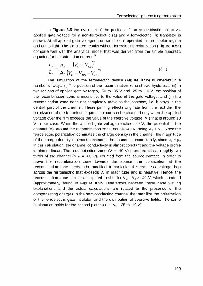
Ferroelectric light emitting transistors
109
In Figure 8.5 the evolution of the position of the recombination zone vs.
applied gate voltage for a non-ferroelectric (a) and a ferroelectric (b) transistor is
shown. At all applied gate voltages the transistor is operated in the bipolar regime
and emits light. The simulated results without ferroelectric polarization (Figure 8.5a)
compare well with the analytical model that was derived from the simple quadratic
equation for the saturation current [3]
:
22
TeDSG
ThG
e
h
e
h
VVV
VV
L
L
(8.1)
The simulation of the ferroelectric device (Figure 8.5b) is different in a
number of ways: (i) The position of the recombination zone shows hysteresis, (ii) in
two regions of applied gate voltages, -50 to -35 V and -25 to -10 V, the position of
the recombination zone is insensitive to the value of the gate voltage, and (iii) the
recombination zone does not completely move to the contacts, i.e. it stays in the
central part of the channel. These pinning effects originate from the fact that the
polarization of the ferroelectric gate insulator can be changed only when the applied
voltage over the film exceeds the value of the coercive voltage (Vc) that is around 10
V in our case. When the applied gate voltage reaches -50 V, the potential in the
channel (V), around the recombination zone, equals -40 V, being VG + Vc. Since the
ferroelectric polarization dominates the charge density in the channel, the magnitude
of the charge density is almost constant in the channel; concomitantly, since μe = μh
in this calculation, the channel conductivity is almost constant and the voltage profile
is almost linear. The recombination zone (V = -40 V) therefore sits at roughly two
thirds of the channel (VDS = -60 V), counted from the source contact. In order to
move the recombination zone towards the source, the polarization at the
recombination zone needs to be modified. In particular, this requires a voltage drop
across the ferroelectric that exceeds Vc in magnitude and is negative. Hence, the
recombination zone can be anticipated to shift for VG - Vc > -40 V, which is indeed
(approximately) found in Figure 8.5b. Differences between these hand waving
explanations and the actual calculations are related to the presence of the
compensating charges in the semiconducting channel that stabilize the polarization
of the ferroelectric gate insulator, and the distribution of coercive fields. The same
explanation holds for the second plateau (i.e. VG: -25 to -10 V).
Chapter 8
110
-50 -40 -30 -20 -102x10
7
3x10⁷
4x10⁷
5x10⁷
Recom
bin
ation C
urr
en
t D
en
sity [
A/m
2]
VG [V]
-50 -40 -30 -20 -101.0x10
8
1.5x10⁸
2.0x10⁸
2.5x10⁸
Re
co
mb
ina
tio
n C
urr
en
t D
en
sity [
A/m
2]
VG [V]
PTrFE P(VDF-TrFE)(a) (b)
-50 -40 -30 -20 -102x10
7
3x10⁷
4x10⁷
5x10⁷
Recom
bin
ation C
urr
en
t D
en
sity [
A/m
2]
VG [V]
-50 -40 -30 -20 -101.0x10
8
1.5x10⁸
2.0x10⁸
2.5x10⁸
Re
co
mb
ina
tio
n C
urr
en
t D
en
sity [
A/m
2]
VG [V]
PTrFE P(VDF-TrFE)(a) (b)
Figure 8.6 Modeling of the recombination current density as a function of gate voltage for a
transistor with a non-ferroelectric (a: ‘PTrFE’) and a ferroelectric (b: ‘P(VDF-TrFE)’) gate
dielectric. Note the different scales of the y-axes in (a) and (b), i.e. ~ 6 times higher current
density in the case of ferroelectric (b), compared to the non-ferroelectric (a) gate.
In Figure 8.6 the recombination currents of the two LEFETs are plotted as a
function of gate voltage. The sweeping scheme is the same as discussed above.
The presence of the ferroelectric (Figure 8.6b) enhances the injection of both
electron and hole currents resulting in more charge recombination as compared to
the non-ferroelectric case (Figure 8.6a). Moreover, in case of the ferroelectric gate
insulator also the recombination current shows hysteresis (Figure 8.6b), which is
consistent with the previously discussed hysteresis in the position of the
recombination zone, shown in Figure 8.5b.
In addition, we also modeled the behavior of less ideal ferroelectric
transistors, i.e. lower mobilities and unbalanced charge transport. We found that the
absolute value of the mobilities is not influencing the position of the recombination
zone. With increasingly unbalanced charge mobilities, however, the hysteresis loop
becomes smaller and the position of the recombination zone remains closer to the
drain contact. ‘Pinning’ of the recombination zone still occurs.
8.8 Conclusions
In summary, a programmable light emitting thin-film transistor is realized
combining a solution-processed polymeric semiconductor and a ferroelectric gate
dielectric. We demonstrate that integration of the ferroelectric dielectric offers a
number of important advantages. Firstly, the charge density in the channel is
increased, resulting in a higher light output. An external quantum efficiency of
1.06 % has been demonstrated, which is ~ 7 times higher than the value obtained
for a similar non-ferroelectric device. Secondly, the light emission also displays a
hysteresis loop, and the device exhibits repeated light programmability. Thirdly,
numerical modeling demonstrates that the position of the recombination zone
becomes less sensitive to small variations in applied gate bias: the remnant
Ferroelectric light emitting transistors
111
polarization charge of the ferroelectric layer ‘pins’ the position of the recombination
zone. The latter opens the way to integrate specific optical out-coupling structures in
the channel of these devices to further increase the brightness. Both the higher
current densities and the possibility to integrate optical out-coupling structures such
as distributed Bragg reflectors may help to reach population inversion which is a
prerequisite for an electrically driven organic laser.
8.9 References
[1] L.-L. Chua, J. Zaumseil, J.-F. Chang, E.C.-W. Ou, P.K.-H. Ho, H. Sirringhaus, R.H. Friend, Nature 2005, 434, 194–199.
[2] J.S. Swensen, C. Soci, A.J. Heeger, Appl. Phys. Lett. 2005, 87, 253511. [3] J. Zaumseil, R.H. Friend, H. Sirringhaus, Nat. Mater. 2006, 5, 69–74. [4] J. Zaumseil, C.L. Donley, J.-S. Kim, R.H. Friend, H. Sirringhaus, Adv. Mater.
2006, 18, 2708–2712. [5] T. Takenobu, S.Z. Bisri, T. Takahashi, M. Yahiro, C. Adachi, Y. Iwasa, Phys.
Rev. Lett. 2008, 100, 066601. [6] R. Capelli, S. Toffanin, G. Generali, H. Usta, A. Facchetti, M. Muccini, Nat
Mater 2010, 9, 496–503. [7] K. Kajiwara, K. Terasaki, T. Yamao, S. Hotta, Adv. Funct. Mater. 2011, 21,
2854–2860. [8] S.Z. Bisri, T. Takenobu, K. Sawabe, S. Tsuda, Y. Yomogida, T. Yamao, S.
Hotta, C. Adachi, Y. Iwasa, Adv. Mater. 2011, 23, 2753–2758. [9] E.B. Namdas, B.B.Y. Hsu, Z. Liu, S. Lo, P.L. Burn, I.D.W. Samuel, Adv.
Mater. 2009, 21, 4957–4961. [10] S. De Vusser, S. Schols, S. Steudel, S. Verlaak, J. Genoe, W.D. Oosterbaan,
L. Lutsen, D. Vanderzande, P. Heremans, Appl. Phys. Lett. 2006, 89, 223504. [11] J. Chang, M. Gwinner, M. Caironi, T. Sakanoue, H. Sirringhaus, Adv. Funct.
Mater. 2010, 20, 2825–2832. [12] M.C. Gwinner, S. Khodabakhsh, H. Giessen, H. Sirringhaus, Chem. Mater.
2009, 21, 4425–4433. [13] M.C. Gwinner, F. Jakubka, F. Gannott, H. Sirringhaus, J. Zaumseil, ACS
Nano 2012, 6, 539–548. [14] M.C. Gwinner, S. Khodabakhsh, M.H. Song, H. Schweizer, H. Giessen, H.
Sirringhaus, Adv. Funct. Mater. 2009, 19, 1360–1370. [15] T. Yamao, Y. Sakurai, K. Terasaki, Y. Shimizu, H. Jinnai, S. Hotta, Adv.
Mater. 2010, 22, 3708–3712. [16] B.B.Y. Hsu, E.B. Namdas, J.D. Yuen, S. Cho, I.D.W. Samuel, A.J. Heeger,
Adv. Mater. 2010, 22, 4649–4653. [17] T. Fukuma, K. Kobayashi, T. Horiuchi, H. Yamada, K. Matsushige, Jpn. J.
Appl. Phys. 2000, 39, 3830–3833. [18] F. Takeo, Adv. Colloid Interface Sci. 1997, 71-72, 183–208. [19] V. Vohra, U. Giovanella, R. Tubino, H. Murata, C. Botta, ACS Nano 2011, 5,
5572–5578. [20] U. Giovanella, P. Betti, C. Botta, S. Destri, J. Moreau, M. Pasini, W. Porzio,
B. Vercelli, A. Bolognesi, Chem. Mater. 2011, 23, 810–816. [21] Z.-Q. Chen, F. Ding, Z.-Q. Bian, C.-H. Huang, Org. Electron. 2010, 11, 369–
376. [22] G. Qian, Z. Zhong, M. Luo, D. Yu, Z. Zhang, Z. Wang, D. Ma, Adv. Mater.
2009, 21, 111–116.

Chapter 8
112
[23] X. Gong, M. Robinson, J. Ostrowski, D. Moses, G. Bazan, A. Heeger, Adv. Mater. 2002, 14, 581–585.
[24] N. Greenham, R. Friend, D. Bradley, Adv. Mater. 1994, 6, 491–494. [25] C. Rooman, Surface-Textured Thin-Film Light-emitting Diodes, PhD Thesis,
IMEC, 2005. [26] J. Zaumseil, C. McNeill, M. Bird, D. Smith, P. Ruden, M. Roberts, M.
McKiernan, R. Friend, H. Sirringhaus, J. Appl. Phys. 2008, 103, 064517. [27] J. Zaumseil, R. Kline, H. Sirringhaus, Appl. Phys. Lett. 2008, 92, 073304. [28] R.C.G. Naber, M. Bird, H. Sirringhaus, Appl. Phys. Lett. 2008, 93, 023301. [29] A.K. Tripathi, A.J.J.M. van Breemen, J. Shen, Q. Gao, M.G. Ivan, K.
Reimann, E.R. Meinders, G.H. Gelinck, Adv. Mater. 2011, 23, 4146–4151. [30] R.C.G. Naber, J. Massolt, M. Spijkman, K. Asadi, P.W.M. Blom, D.M. de
Leeuw, Appl. Phys. Lett. 2007, 90, 113509. [31] K. Asadi, P. de Bruyn, P.W.M. Blom, D.M. de Leeuw, Appl. Phys. Lett. 2011,
98, 183301. [32] J. Zaumseil, H. Sirringhaus, Chem. Rev. 2007, 107, 1296–1323. [33] A.K. Tripathi, E.C.P. Smits, M. Loth, J.E. Anthony, G.H. Gelinck, Appl. Phys.
Lett. 2011, 98, 202106. [34] H. Nalwa, Ferroelectric Polymers: Chemistry, Physics, and Applications, M.
Dekker Inc., New York 1995. [35] C. Black, C. Farrell, T. Licata, Appl. Phys. Lett. 1997, 71, 2041–2043. [36] T. Ma, J. Han, IEEE Electron Device Lett. 2002, 23, 386–388. [37] M. Kemerink, D.S.H. Charrier, E.C.P. Smits, S.G.J. Mathijssen, D.M. de
Leeuw, R.A.J. Janssen, Appl. Phys. Lett. 2008, 93, 033312. [38] L. Wang, J. Yu, Y. Wang, G. Peng, F. Liu, J. Gao, J. Appl. Phys. 2007, 101,
104505. [39] C.H. Tsang, C.K. Wong, F.G. Shin, J. Appl. Phys. 2005, 98, 084103. [40] I.P. Batra, P. Wurfel, B.D. Silverman, Phys. Rev. B 1973, 8, 3257–3265. [41] P. Wurfel, I.P. Batra, Phys. Rev. B 1973, 8, 5126–5133. [42] V. Khikhlovskyi et al., 2012, manuscript in preparation.
113
Summary
Controlling Morphology and Molecular Order of Solution-Processed Organic
Semiconductors for Transistors
As a potential low-cost alternative to traditional amorphous-silicon based
devices, organic field-effect transistors (OFETs) are expected to be incorporated into
all-plastic integrated circuits and flexible display backplanes. More recently,
breakthroughs have been made in the performance of OFETs based on π-
conjugated small molecules, among which, tri-isopropylsilylethynyl pentacene (TIPS-
PEN) and its derivatives are currently under extensive investigations due to their
good charge-transport properties combined with decent air-stability, as well as the
possibility of inexpensive solution-processing. Fundamental understanding of the
charge transport is not only important to deepen the understanding of structure-
property relationships of organic functional layers, but also to optimize the
performance of various organic electronic devices. The charge-carrier mobility is a
critical parameter for the operating speed of a device, notably, in an OFET.
Structural inhomogeneity within a single component or between phase-separated
blends has a significant impact on the local charge-transport properties. Thus,
controlling the morphology and molecular order of organic semiconductors is the key
to achieve optimal performance for OFETs.
This thesis is aiming at highly reproducible solution-processed organic
transistors, with device parameters relevant to practical applications (e.g. low
operating-voltages, steep sub-threshold slopes and uniform performance in large
areas), through controlling the morphology and molecular order of small-molecule
organic semiconductors. More specifically, this thesis intends to achieve a balanced
combination of (i) a solvent-based processing method that can manipulate the
morphology of organic semiconductors; (ii) a composite semiconductor formulation
consisting of TIPS-PEN and a binder material such as a polymer; (iii) use of
patterning methods in line with the requirements of large-area electronics, such as
ink-jet printing; and (iv) an improved understanding of charge-transport mechanisms
in (realistic) high-performance transistor devices based on these single-component
or composite semiconductors. This combination results in highly reproducible
solution-processed OFETs exhibiting high mobility as well as decent uniformity in
large areas, as demonstrated throughout the thesis.
Aiming at the first objective (i) of this thesis, in Chapter 2, a new approach
was developed to prepare large single crystals of organic semiconductors, by using
azeotropic binary solvent mixtures. The two solvents form a positive azeotrope and
have significantly different solubilities for TIPS-PEN. At solvent compositions close
to the azeotropic point, an abrupt transition of morphology from polycrystalline thin-
films to large single crystals was observed. We found that the solvent composition at
the late-stage of evaporation determines the final morphology, which can be facilely
Summary
114
controlled by adjusting the initial volume ratio of the binary solvents. The charge-
carrier mobilities were substantially enhanced by a factor of 4, from the morphology
of thin-films to large single crystals used as active layer in OFETs. Additionally, this
approach was extended to other π-conjugated organic molecules to elucidate its
broad applicability.
To achieve a balanced combination of the objectives (ii) & (iii), i.e. large-
area patterning of composite semiconductors, next, we set out to study the effects of
blending an organic semiconductor with an insulating polymer on the morphology
and transistor performance. In Chapter 3 we presented a systematic study of the
influence of material composition and ink-jet processing conditions on the charge
transport in bottom-gate/bottom-contact OFETs based on single droplets of TIPS-
PEN/polystyrene blends. After careful process optimization of blending ratio and
printing temperature we routinely make transistors with an average mobility of 1
cm2/Vs (maximum 1.5 cm
2/Vs), on/off ratio exceeding 10
7, sharp turn-on in current
(sub-threshold slopes approaching 60 mV/decade, the second steepest value for
OFETs reported so far), and decent uniformity in large areas. These characteristics
are superior to the neat TIPS-PEN devices. Using channel scaling measurements
and scanning Kelvin probe microscopy, the sharp turn-on in current in the blends
was attributed to a contact (tunneling) barrier that originates from a thin insulating
polystyrene layer between the injecting contacts and the semiconductor channel.
These new insights on device operations of our blend transistors provide valuable
guidelines towards next-generation organic transistors based on small-molecule
semiconductor and insulating polymer blends.
Following the knowledge gained in Chapter 3, and in line with the objective
(iv) of this thesis on the fundamental understanding of device operation, a so-called
‘electric field confinement effect’ on charge transport in polycrystalline OFETs was
presented in Chapter 4. It is known that the charge-carrier mobility in organic
semiconductors is only weakly dependent on the electric field at low fields; our
experimental charge-carrier mobility in OFETs using TIPS-PEN was found to be
surprisingly field-dependent at low source-drain fields. Corroborated by scanning
Kelvin probe measurements, we explained this experimental observation by the
severe difference between the local lateral-field dependences within grains and at
grain boundaries. Redistribution of accumulated charges creates very strong local
lateral fields in the latter regions. These strong local fields in the grain boundaries
result in the carrier mobility in grain boundaries to become field-dependent, and as
the mobility in grain-boundaries limits the overall mobility its field-dependence
translates to a field-dependence of the average mobility. We further confirmed this
picture by verifying that the charge-carrier mobility in channels having no grain
boundaries, made from the same type of organic semiconductor, is not significantly
field-dependent. Finally, we showed that our model allows us to ‘quantitatively’
describe the source-drain field dependence of mobility in polycrystalline OFETs.
Then, we moved to using molecular design to control the morphology and
molecular order of organic semiconductors. In Chapter 5 we presented a new TIPS-
PEN derivative, namely BTE-TIPS-PEN, with ethyl substituents at the 2,3,9,10
Summary
115
backbone positions to modulate the solubility and film-forming properties. High-
performance OFETs were readily fabricated using a single-step process without the
need to form blends or the use of top-gate architecture. Average mobilities above 1
cm2/Vs were measured at low-operating voltages for specific crystal orientations,
with the highest saturation mobility reaching as high as 3.92 cm2/Vs, confirming that
an improved molecular design can indeed result in a controlled macro- and micro-
structure of BTE-TIPS-PEN thin films that positively influences the electronic
properties. The high device reproducibility obtained for BTE-TIPS-PEN is also
promising for the technological exploitation of such discrete devices in large-area
organic electronics.
Next, we demonstrated in Chapter 6, that a careful selection of the casting
temperature alone can allow a rapid production of OFETs with uniform and
reproducible device performance over large areas. Based on a systematic
investigation on the thermal behaviour of 5,11-bis(triethyl silylethynyl)
anthradithiophene (TES ADT), we presented four distinctive solid-state phases of
TES ADT exhibiting drastically different charge-transport properties, deduced from
OFET device characteristics corroborated by Lateral Time-of-Flight (L-ToF)
photoconductivity measurements. The best-performing crystal polymorph of TES
ADT was identified: when casting solutions of TES ADT dissolved in chloroform at a
substrate temperature of more than 20 °C below its glass transition temperature,
highly-crystalline and homogeneous TES ADT thin films can be facilely produced in
a single-step, without the need for any post-depositions as previously reported,
opening pathways towards high-throughput and reliable fabrication of high-
performance OFETs.
In Chapter 7 we presented the first highly-reproducible n-type SAMFET,
based on a perylene derivative (namely PBI-PA) with a phosphonic acid anchoring
group which enables an efficient fixation to aluminum oxide. Simple device
fabrication under ambient conditions leads to a complete surface coverage of the
aluminum oxide with a monolayer of PBI-PA, and to transistors with electron
mobilities up to 10-3
cm2/Vs for channel length as long as 100 μm. By implementing
p- and n-type SAMFETs in one circuit, a complementary inverter based solely on
SAMFETs, with a large noise margin of 7 volts and a gain up to 17, was
demonstrated for the first time, paving the way to robust and low-power self-
assembled monolayer based complementary circuits.
In addition, in Chapter 7 we (surprisingly) found that our PBI-PA forms a
‘nano-crystalline’ structured SAM with no long range in-plane order. Despite this,
highly-reproducible SAMFETs with a decent electron mobility of 10-3
cm2/Vs were
still achieved. This seems contradicted to the previously demonstrated p-type
SAMFETs based on quinquethiophene derivative attached on silicon dioxide, where
a long range (at least over several micrometers) in-plane order was believed to be
the prerequisite to form the semiconducting SAM. This comparison gives an
immediate consequence on how we should better understand the requirement and
working principle of SAMFETs: here we propose that as long as the chemical
anchoring (covalent bonding) of our PBI-PA molecules onto aluminum oxide surface
Summary
116
is taking place effectively, we can achieve a reasonably well-semiconducting
monolayer without long range in-plane order. The fact that the mobilities in our n-
type SAMFETs were still one order of magnitude lower than the previous p-type
SAMFETs is most likely due to the lower degree of π-orbital overlaps caused by the
nano-crystalline nature of our PBI-PA SAM, in conjunction with the severely contact-
limited electron transport using Au as the charge-injecting electrodes here.
Therefore, a further improvement on device performance addressing these two
issues can be clearly envisioned.
As a side topic of this thesis, in the last Chapter, we introduced an
unconventional use of the molecular (polymer chain/dipole) alignment, in the
dielectric layer of organic field-effect transistors. Chapter 8 presented a voltage-
programmable light-emitting field-effect transistor (LEFET) using a ferroelectric
polymer as the gate dielectric. We showed by both experimental observations and
numerical modeling that, when the ferroelectric gate dielectric is polarized in
opposite directions at the drain and source sides of the channel, respectively, both
electron and hole currents are enhanced, resulting in more charge recombination
and ~ 10 times higher light emission in a ferroelectric LEFET, compared to the
device with non-ferroelectric gate. As a result of the ferroelectric poling (dipole
alignment), our ferroelectric LEFETs exhibit repeated programmability in light
emission, and an external quantum efficiency (EQE) of up to 1.06 %. Numerical
modeling revealed that the remnant polarization charge of the ferroelectric layer
tends to ‘pin’ the position of the recombination zone, paving the way to integrate
specific optical out-coupling structures in the channel of these devices to further
increase the brightness.
The results and new insights obtained in this thesis will serve as important
guidelines for the development of new generation solution-processed organic
transistors towards large-area organic (opto-) electronics.
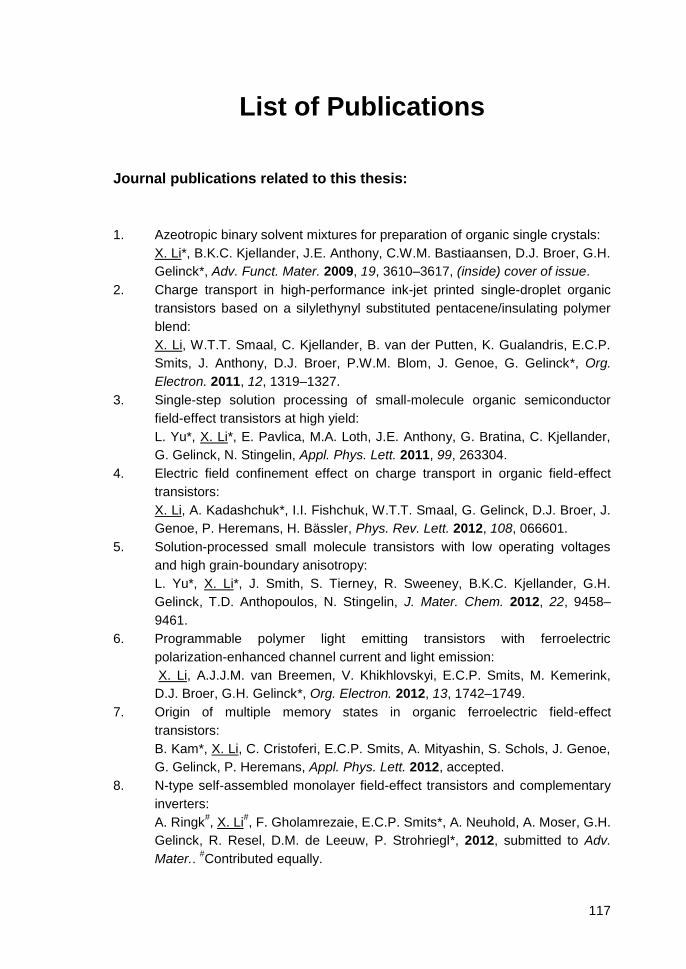
117
List of Publications
Journal publications related to this thesis:
1. Azeotropic binary solvent mixtures for preparation of organic single crystals:
X. Li*, B.K.C. Kjellander, J.E. Anthony, C.W.M. Bastiaansen, D.J. Broer, G.H.
Gelinck*, Adv. Funct. Mater. 2009, 19, 3610–3617, (inside) cover of issue.
2. Charge transport in high-performance ink-jet printed single-droplet organic
transistors based on a silylethynyl substituted pentacene/insulating polymer
blend:
X. Li, W.T.T. Smaal, C. Kjellander, B. van der Putten, K. Gualandris, E.C.P.
Smits, J. Anthony, D.J. Broer, P.W.M. Blom, J. Genoe, G. Gelinck*, Org.
Electron. 2011, 12, 1319–1327.
3. Single-step solution processing of small-molecule organic semiconductor
field-effect transistors at high yield:
L. Yu*, X. Li*, E. Pavlica, M.A. Loth, J.E. Anthony, G. Bratina, C. Kjellander,
G. Gelinck, N. Stingelin, Appl. Phys. Lett. 2011, 99, 263304.
4. Electric field confinement effect on charge transport in organic field-effect
transistors:
X. Li, A. Kadashchuk*, I.I. Fishchuk, W.T.T. Smaal, G. Gelinck, D.J. Broer, J.
Genoe, P. Heremans, H. Bässler, Phys. Rev. Lett. 2012, 108, 066601.
5. Solution-processed small molecule transistors with low operating voltages
and high grain-boundary anisotropy:
L. Yu*, X. Li*, J. Smith, S. Tierney, R. Sweeney, B.K.C. Kjellander, G.H.
Gelinck, T.D. Anthopoulos, N. Stingelin, J. Mater. Chem. 2012, 22, 9458–
9461.
6. Programmable polymer light emitting transistors with ferroelectric
polarization-enhanced channel current and light emission:
X. Li, A.J.J.M. van Breemen, V. Khikhlovskyi, E.C.P. Smits, M. Kemerink,
D.J. Broer, G.H. Gelinck*, Org. Electron. 2012, 13, 1742–1749.
7. Origin of multiple memory states in organic ferroelectric field-effect
transistors:
B. Kam*, X. Li, C. Cristoferi, E.C.P. Smits, A. Mityashin, S. Schols, J. Genoe,
G. Gelinck, P. Heremans, Appl. Phys. Lett. 2012, accepted.
8. N-type self-assembled monolayer field-effect transistors and complementary
inverters:
A. Ringk#, X. Li
#, F. Gholamrezaie, E.C.P. Smits*, A. Neuhold, A. Moser, G.H.
Gelinck, R. Resel, D.M. de Leeuw, P. Strohriegl*, 2012, submitted to Adv.
Mater.. #Contributed equally.
List of Publications
118
9. Influence of solid-state microstructure on the electronic performance of 5,11-
bis(triethylsilylethynyl) anthradithiophene:
L. Yu*, X. Li*, E. Pavlica, F. Koch, G. Portale, M.A. Loth, J.E. Anthony, P.
Smith, G. Bratina, B.K.C. Kjellander, C.W.M. Bastiaansen, D.J. Broer, G.H.
Gelinck, N. Stingelin, 2012, submitted to Adv. Mater..
10. Origin of steep sub-threshold slope in high-performance ink-jet printed
organic transistors studied by current-sensing scanning probe microscopy:
X. Li*, P. Graat*, J. Genoe, B.K.C. Kjellander, W.T.T. Smaal, C.W.M. Bastiaansen, D.J. Broer, G.H. Gelinck, 2012, manuscript in preparation.
Journal publications and patent not related to this thesis:
11. Microcontact printing of self-assembled monolayers to pattern the light-
emission of polymeric light-emitting diodes:
J. Brondijk#, X. Li
#, H. Akkerman, P. Blom, B. de Boer*, Appl. Phys. A: Mater.
Sci. Process. 2009, 95, 1–5. #Contributed equally.
12. A novel approach of preparation and patterning of organic fluorescent
nanomaterials:
L. Zhao*, Z. Lei, X. Li, S. Li, J. Xu, B. Peng, W. Huang*, Chem. Phys. Lett.
2006, 420, 480–483.
13. Vacuum thermal evaporation film-forming method using strong electric field:
W. Huang*, G. Xing, X. Li, G. Zhong, J. Xu,
Chinese Patent (Application NO. CN 200410066241),
Date of Application: 9/Sep/2004; Date of Publication: 6/Feb/2008.
Oral presentations at international/national conferences related to this
thesis:
1. High-performance ink-jet printed single-droplet transistors based on a small
molecule/insulating polymer blend for large-area organic electronics:
X. Li, W.T.T. Smaal, P. Graat, C. Kjellander, B. van der Putten, E.C.P. Smits,
J. Anthony , D.J. Broer, P.W.M. Blom, J. Genoe, G. Gelinck
at the 2011 Materials Research Society (MRS) Fall Meeting, Boston, USA,
28/Nov/2011 – 2/Dec/2011.
List of Publications
119
2. Charge transport in high-performance ink-jet printed single-droplet transistors
based on a small molecule/insulating polymer blend:
X. Li, W. Smaal, P. Graat, C. Kjellander, B. van der Putten, E. Smits, J.
Anthony, C.W.M. Bastiaansen, D.J. Broer, P. Blom, J. Genoe, G. Gelinck
at the 2012 Dutch Polymer Days, Lunteren, The Netherlands, 12/Mar/2012 –
13/Mar/2012.
3. A programmable polymer light-emitting transistor with enhanced channel
current and light emission:
X. Li, A.J.J.M. van Breemen, V. Khikhlovskyi, E.C.P. Smits, M. Kemerink,
D.J. Broer, G.H. Gelinck
at the International Conference on Science and Technology of Synthetic
Metals 2012 (ICSM 2012), Atlanta, USA, 8/Jul/2012 – 13/Jul/2012.
4. Electric field confinement effect on charge transport in polycrystalline organic
field-effect transistors:
X. Li, A. Kadashchuk, I.I. Fishchuk, W.T.T. Smaal, G. Gelinck, D.J. Broer, J.
Genoe, P. Heremans, H. Bässler
at the 11th Junior Euromat Conference (JUNIOR EUROMAT 2012),
Lausanne, Switzerland, 23/Jul/2012 – 27/Jul/2012.

120
Acknowledgements Towards the end of this thesis, now I would like to use the last pages to express my
sincere gratitude and appreciation to everyone who has contributed, in one way or another, to
the completions of this thesis and my PhD project.
First, I owe my deepest gratitude to my supervisor and co-supervisors: Prof. Dick
Broer, Prof. Kees Bastiaansen, and Dr. Gerwin Gelinck. Thank you all so much for giving me
the great privilege of working on this exciting research topic, as well as your inspiring and
critical scientific instructions on my work! The unique setting of my PhD project has offered
me full access to state-of-the-art facilities, ample exposures to both academic and industrial
research environments, and precious opportunities of working with a number of brilliant
scientists at several top-class institutes. Meanwhile, working at both groups of SFD (TU/e)
and TP5 (Holst Centre) is simply enjoyable, thanks to their excellent research and amazing
extracurricular activities. Dick, no words can fully express my heartfelt appreciations to you. I
feel so lucky and grateful to have you as the supervisor of my project, and equally important,
as my mentor. During the past four years, your constructive and timely supervision over the
project has inspired me and generated many new ideas; meanwhile your kindness, patience,
and thoughtful considerations have helped me out on numerous occasions. Moreover,
besides the work, you have also pointed to me the importance of a work-life balance, and
even paved ways for me to improve it, although so far my progress on this is still a bit
disappointing... Now, towards the end of this PhD journey and looking back, I hope you have
also liked having me as one of your students, and from this point I will try my best to find a
better balance between work and life. Kees, as my co-supervisor at the TU/e, your constant
support and timely instruction for the project have been invaluable to me, and critical to the
smooth completion of this PhD, even when I was not around (in most cases only five
kilometers away from the TU/e though). I have also learnt a lot from you over these years:
your inquisitive approach to every discussion we had and each presentation I delivered, and
your critical and timely advice on my progress, have not only broadened my scientific horizon,
but also ‘dragged’ me back to the right track from time to time. And I really appreciate your
great patience on correcting my thesis over and over, your suggestions were critical for
improving its over-all quality, and I believe this thesis has become more ‘reader-friendly’ by
now. Gerwin, as my daily co-supervisor at the Holst Centre, your scientific contributions to this
thesis is indispensable and I am deeply in debt to you. Besides offering me timely instructions
and advice for the project on a regular basis, you have always pointed me to the right
direction. And I have learnt a great deal from you in many aspects of being an excellent
scientist: your critical scientific approaches, innovative thinking, and ways of nurturing and
generating great ideas have really intrigued me. I also appreciate you a lot for showing me
how to deliver a high-impact scientific presentation, and teaching me that ‘writing a good
paper is like making a good wine, and good wine takes time’. I hope you have also perceived
my growth through these years, and liked having me as the very first PhD student you have
directly supervised.
Next, I would like to deliver my sincere gratitude to the other members of my reading
committee: Prof. Paul Blom, Prof. Dago de Leeuw, and Prof. René Janssen. Thank you all
very much for your prompt responses, constructive comments, and timely approvals to this
thesis, improving and reassuring its scientific quality! Paul, your long-term support to me
dates back to my master study in Groningen and through the entire period of my PhD in
Eindhoven, thank you so much for everything. Dago, I am so grateful to you for all the
intriguing discussions and helpful suggestions you have given me all these years, and
especially your great support for our SAMFET project in chapter 7, thank you very much.
René, your scientific insights into supermolecular aggregations and the related optical
Acknowledgements
121
spectroscopy have guaranteed the quality of chapter 2, and I feel so lucky and privileged to
have you in my committee, thank you so much.
Besides the generous funding for this PhD project from the Holst Centre and TU/e,
the financial supports from many EU projects are also gratefully acknowledged here: the
European Community’s Seventh Framework Programme (FP7/2007-2013) under grant
agreements No. 212311 of the ONE-P project, No. 216546 of the FLAME project, No. 248092
of the MOMA project, and No. 247978 of the POLARIC project.
Like many others, this thesis is a collective result of very close and fruitful
collaborations among many talented researchers from several distinguished academic groups,
research institutes, and industrial partners worldwide. Hereby I would like to deliver my
heartfelt gratitude and appreciations to each and every one of them, some of whom I will
mention in particular below.
Charlotte, as my daily coach at the beginning, the advisor through my project and at
my upcoming defense, also as my office mate for almost four years, here are my special
appreciations to you. Thank you for introducing me to all the lab equipments at Holst when I
first started, for constantly encouraging, and patiently advising me whenever I encountered
difficulties. Over the years you have helped me overcome many obstacles towards this point,
and I don’t think I could have ‘survived’ this PhD without your great support all the time! I wish
you every success in your career, and all the best! Wiljan, my buddy, I have missed you so
much since you moved to Bordeaux. Thank you so much for helping me out on various
occasions through almost three quarters of my PhD! The countless hours of ‘overtime’ we
spent in the office were a lot easier for me with your delightful company. Equally important,
without your crucial contributions to the ink-jet printing, chapters 3 and 4 would never have
been possible. Now I wish you a wonderful life (with your girl) in France, and look forward to
catching up with you soon! Edsger, I have owed you so much for your indispensable help for
many important results obtained in chapters 8 and 3, together with your great passion and
patience on instructing our work for chapter 7. And I have realized that as the expert on both
SAMFETs and ambipolar organic transistors, you have indeed offered me the very best help
and supervisions I could ever wish for, thank you so much! Bas, your fantastic technical
supports and daily maintenance of our cleanroom were indispensable to all my experimental
work at Holst, meanwhile I have also learnt a great deal from you with your almost twenty
years of experiences on various processing techniques. More importantly, thank you so much
for patiently providing me over the last four years with countless device substrates, most of
which have brought us brilliant results!
I was in a very lucky position of having the opportunity to work with very talented
theoreticians: Andrey, I am deeply in debt to you. Thank you so much for coming up with the
brilliant idea as the foundation of chapter 4, for the beautiful modelling work performed by
your group in Kiev, and for your unremitting efforts on pushing our paper published. I hope to
meet you soon again around Eindhoven! Seva, thank you so much for your brilliant modelling
and hard work for chapter 8, those hours of discussion we had even beyond the scope of
science will be unforgettable to me! And I wish you every success in your career, and an
enjoyable PhD time! Martijn, I owe my heartfelt thanks to you, for your insights into the topic of
ferroelectrics, critical contributions to chapter 8, and helpful comments on our manuscript.
At the IMEC part of TP5 in Leuven, I am deeply in debt to Prof. Paul Heremans and
Prof. Jan Genoe, for their critical scientific contributions to chapters 4 and 3, constant support
and intriguing comments to my project, and great patience and efforts on publishing chapter 4.
Paul and Jan, thank you so much for everything!
Liyang, I am so grateful to you for all the beautiful work we did together for chapters
5 and 6. You are simply the master for processing TES ADT and BTE-TIPS-PEN, and I have
learnt a great deal from you. Thank you for showing me around the city of London during my
stay at Imperial, and I have really missed the Chinese restaurants over there! I wish you all
Acknowledgements
122
the best for the final stage of your PhD as well! Natalie, as THE expert on material processing
and related phase behaviors, etc., your scientific contributions to chapters 5 and 6 were
indeed critical. I am so grateful to have such a precious opportunity to learn from you in many
aspects. And thank you so much for kindly accommodating me in your group at Imperial
College London in 2010, and your great hospitality and support to me all the time! My thanks
also go to the other members in the ‘PiCOS’ cluster from DPI: Dr. John van Haare, Prof.
Anton Darhuber, and Dr. Rafal Rogowski.
Andreas, I was so lucky and grateful to work with you on this exciting new SAM
molecule in chapter 7, you are simply the best chemist I know on perylene bisimide! Also
thank you for allowing me to use some of the beautiful images you prepared, and those long
hours we spent together in the cleanroom of Holst are absolutely memorable, and tons of fun
to me! I also wish you every success for the last stage of your PhD!
Special thanks also go to the experts at the (former) Philips MiPlaza: Cees for the
XPS; Emile for the FTIR and Raman; Hugo for the GC-MS; René for the AFM; Harry for the
XRD; Tom for preparing the nice ‘BIO1’ substrates; and Ton for helping me in the MiPlaza
cleanroom. Peter, I owe you my heartfelt thanks in particular! Your very patient and effective
instructions to me for using the SKPM and C-AFM setups at the MiPlaza have enabled many
crucial and beautiful results for chapters 3 and 4. I have learnt a lot from you and thank you
so much for your constant support! And next I will try my best to finish our paper asap.
I would like to deliver my heartfelt thanks to Prof. John Anthony at the University of
Kentucky. John, thank you so much for generously providing us with sufficient amounts of key
materials (TIPS-PEN, TES ADT, and diF-TES ADT) used in many chapters of this thesis, and
for your always timely and constructive comments on the manuscripts we have collaborated
on. Special thanks also go to Jorgen Sweelssen at TNO for providing me with some of the
best-quality materials (e.g. F8BT and TIPS-PEN). Thanks to Merck Chemicals Ltd. at
Southampton for the generous supply of BTE-TIPS-PEN; and thanks to Solvay Specialty
Polymers for constantly providing us with P(VDF-TrFE) and PTrFE materials.
I also would like to thank everyone in the group of Prof. Dago de Leeuw at Philips
Research Eindhoven, especially Anne-Marije, Christian, Kamal, Mark-Jan, and Paul. And my
heartfelt thanks to Simon for kindly sharing his profound knowledge and experience with me
on SKPM; to Fatemeh for generously helping us with the p-type SAMFET samples; and to
Mengyuan for her kind support and inspiring conversations all the time.
Then, I would like to take this opportunity to acknowledge all the other collaborators
and co-authors in our publications, for their brilliant and indispensible contributions to this
thesis: Kevin Gualandris (chapter 3); Dr. Ivan Fishchuk and Prof. Heinz Bässler (chapter 4);
Dr. Jeremy Smith, Dr. Steven Tierney, Dr. Richard Sweeney, and Dr. Thomas Anthopoulos
(chapter 5); Dr. Egon Pavlica, Dr. Marsha Loth, Felix Koch, Dr. Giuseppe Portale, Prof. Gvido
Bratina, and Prof. Paul Smith (chapter 6); Dr. Alfred Neuhold, Armin Moser, Prof. Roland
Resel, and Prof. Peter Strohriegl (chapter 7). Thank you so much for the nice collaborations!
At the Holst Centre, my sincere gratitude also goes to all the other group members of
TP5 in Eindhoven: to Albert for answering all my questions about the chemistry of P(VDF-
TrFE), etc.; to Ashutosh for providing me with some very interesting GIZO samples to
measure, and the nice conversations we had; to Brian for helping me improve my MRS talk,
and the useful tips for English writing; to Aashini, Abhi, and Jan-Laurens for sharing their
wisdoms and experiences with me during and after work; and to Francisco for his constant
support to me, and all the funny jokes we had! Hangxing, my special thanks to you as well for
sharing all your wisdoms and tips for becoming a successful PhD, which has made this last
stage of my PhD much smoother! Also I would like to thank all the other TP5 members at the
IMEC in Leuven, in particular, thanks to Benjamin for helping me better understand
ferroelectrics, and the challenging but rewarding SKPM experiments we did together; to Kris
for sharing his experience on Igor program, and teaching me some fundamentals on circuits;

Acknowledgements
123
to Sarah for finding me an important reference in chapter 8; to Robert for providing me with
another interesting material (PXX) to test; to Tung Huei for the stimulating discussions on
chapter 8; to Soeren for helping us with the cryo-probestation at IMEC; and to Wan-Yu for the
nice trip during our ONE-P summer school in Italy. And I also want to thank Dr. Martin
Thornton and Dr. Christoph Sele for their great support to me at the earlier stage of my PhD.
My heartfelt thanks also go to everyone else at Holst Centre who has helped me on
numerous occasions: to Dr. Jasper Michels for teaching me the fundamentals of phase-
separation; to Gert van Heck for helping me with the photodiode; to Dr. Marc Koetse for
finding me the special optic fiber ‘connector’; to Juan Diego for instructing me on the optic
fiber spectrometer; to Dr. Mária Peter for providing me a nice PDMS template; to Dr. Marius
Ivan for the interesting ‘Friday afternoon project’ we had; to Arjan Langen and Roel Kusters
for their kind support at the cleanroom of Holst; to Peter Giesen for some very nice company
at my overtime in the office; to Bart Paeper for timely helping me move my PC and network;
and of course to my ‘old’ friends at Holst from my Groningen time: Hylke, Date, and Irina, and
to anyone else I might have forgotten. My fellow PhD students at Holst: Pieter Moonen and
Gari Arutinov, the wonderful visit (and the MRS of course) we had at Boston is unforgettable,
and I wish both of you every success! My gratitude also goes to some of the (former)
internship students at Holst for the good time we had together: Ronggang, Jie, Yongbin, Rui,
Umar, Uyxing, Swathi, Santhosh, Ali, Nouman, Qi, Muhammad, Usman, and the others.
At the chemistry department of TU/e, I owe my grateful thanks to Pauline Schmit and
Anne Spoelstra for their great help with the SEM and TEM measurements, to Marco Hendrix
for the XRD characterizations, and to Dr. Weizhen Li for her help with the DSC measurements.
I would like to express my sincere gratitude to the entire SFD (former PICT) group at
the TU/e. In particular, many thanks to Altug, Amol, An, Antonio, Casper, Danqing, Debarshi,
Helena, Irén, Ivelina, Jelle, Joost, Katherine, Ko, Laurens, Mian, My, Natalia, Paul, Pit, Robert,
Shufen, Ties, Tom, and Youseli; also to Rafiq, Tamara, and Yogesh from the SKT group, and
to anyone else I might have forgotten. I was so lucky to have you guys around at the TU/e,
and I have enjoyed the time we spent together and learnt a lot from you all, both in the lab
and outside of work. And of course I owe my gratitude to our very kind and supportive
secretaries at the SFD and the former PICT: Marjolijn, Elly, and Ineke; also to our financial
officer Matthijs Lodewijks for his great patience and constant support to me. I also want to
thank Dr. Albert Schenning and Dr. Michael Debije for their inspiring comments on my
presentations given at the TU/e, and their long-term interests shown on my project. Albert,
also thank you for your great help on the temperature/concentration-dependent UV/Vis
spectra measurements! And special thanks to everyone who has comforted and encouraged
me when I encountered the frustrations (over and over) by the ‘peer reviewing’ system…
I also owe my thanks to the other friends of mine who have made Eindhoven and
Holland a nice and fun place for me to live: Ruiju Gao, Jiaqi Chen, Yang Gao, Kelly Yang, Xixi
Lu, Donglin Tang, Piming Ma, Wei Xu, Xiongchuan Huang, and others I might have forgotten
from Eindhoven; also to Ilias, Jia, Mingtao, Yuan, Johan, and the others from Groningen: I still
miss the great time we had in MEPOS, and look forward to seeing you guys again soon!
Last, but surely not the least, the weekly ‘Skype’ conversations with my parents back
in Shanghai have made this long journey of PhD abroad a lot easier. Mom and dad, this
thesis is dedicated to both of you, for your unconditional love to me ever since I was born
(thirty years ago…). Through all these days and nights we could not see each other; however,
your complete understanding, absolute trust, and constant support have become my
motivations to pursue excellence, and to be a better person. Everyday I am trying to convey
my words of gratitude into actions. Now, just before I start my professional career, mom and
dad, I wish you two together a healthy, relaxing, and colorful life of retirement!
Xiaoran Li
Eindhoven, 2012 summer
124
Curriculum Vitae
Xiaoran Li was born on May 29th, 1982 in Heilongjiang, China. After obtaining
Bachelor of Science degree in July 2004 at the Department of Illumination
Engineering and Light Sources, Fudan University, Shanghai, China, he entered the
field of organic electronics as a Master of Science candidate at the Laboratory of
Advanced Materials of the same university. In September 2006 he was enrolled
(with full scholarships) to the Top Master Programme in Nanoscience at the Zernike
Institute for Advanced Materials, University of Groningen (RuG), Groningen, The
Netherlands, where he did his Master thesis project in the group of Prof. Paul Blom,
on micro-contact printing of self-assembled monolayers to pattern the light-emission
of polymeric light-emitting diodes.
From September 2008 he started his PhD project on controlling the morphology and
molecular order in solution-processed organic transistors towards large-area opto-
electronics, of which the major results are presented in this thesis. This PhD
research was carried out within the 3TU framework, in the group of Prof. Dick Broer
(SFD) at the Department of Chemical Engineering and Chemistry, Eindhoven
University of Technology (TU/e), and jointly in the group of Organic and Oxide
Transistors (TP5) led by Dr. Gerwin Gelinck at the Holst Centre/TNO, Eindhoven,
The Netherlands.