Embed Size (px)
Citation preview
Solar Cells, 25 (1988) 73 - 89 73
COMPUTER SIMULATION OF THE EFFECTS OF ELECTRICAL MISMATCHES IN PHOTOVOLTAIC CELL INTERCONNECTION CIRCUITS
J. W. BISHOP
ESTI Project, Commission o f the European Communities Joint Research Centre, 21020 ispra, Varese (Italy)
(Received June 20, 1988)
Summary
A Pascal program, PVNet, has been developed at the Commission of the European Communit ies Joint Research Centre, Ispra, to model the electrical behaviour of solar cell interconnection circuits. The program calculates three-quadrant solar cell current-voltage (I-V) curves using a lumped param- eter equivalent circuit model, combines them to obtain the resultant I -V curve of any interconnection circuit, and calculates the operating point of each circuit element, set b y user<tefined operating conditions. The numerical values of the equivalent circuit parameters are generated by the program, and are varied so that the electrical parameters (short-circuit current, open-circuit voltage, fill factor) of calculated I -V curves show the same variations as those of measured crystalline silicon solar cell I -V curves. Equivalent circuit param- eters can be changed by the user, making it possible to simulate the effects of electrical mismatches on the performance of an interconnection circuit. To illustrate the operat ion of the program, the electrical mechanisms leading to hot-spot heating in photovoltaic arrays are analysed. Three types of inter- connect ion circuit are considered: a simple series string, a series-parallel block and a series connect ion of series-parallel blocks. The operat ion of parallel bypass diodes (used to limit hot-spot heating in series strings) and of series blocking diodes (used to prevent current imbalance in series-parallel circuits) are explained.
1. Introduct ion
Photovoltaic arrays are networks of electrical generators, the smallest of which are individual solar cells. Array performance is optimized by ensuring that all the generators are electrically matched, i.e. that they all develop the same currents or voltages, depending on whether they are connected in series or in parallel. Electrical mismatches, due to shadowing or cell damage, reduce array efficiency and cause hot-spot heating -- a faulty mode of opera-
0379-6787/88/$3.50 © Elsevier Sequoia/Printed in The Netherlands
74
tion which can damage cell encapsulation materials, permanently reduce array power output and even put arrays out of action.
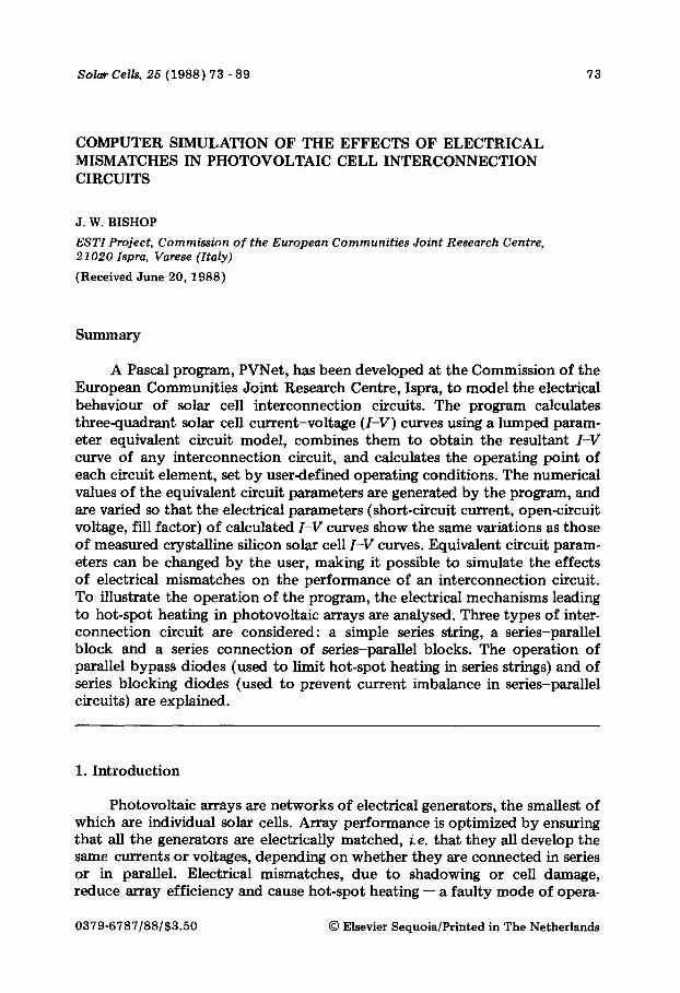
The effects of electrical mismatches and component failures on the performance of an array are limited by redundant circuit design (see Fig. 1) [1, 2]. Arrays are divided into parallel branch circuits, consisting either of a single series string or several strings in parallel. Blocking diodes prevent forward biasing of voltage-mismatched branch circuits. Multiple connections between individual cells and the use of bypass diodes allow series strings to function in the presence of open-circuit failures. Bypass diodes also limit the reverse biasing of current-mismatched cells [3, 4]. Series paralleling, in which cross-ties connect adjacent strings and divide a branch circuit into series blocks, reduces the effects of electrical mismatches. One or more series blocks can be bridged by a bypass diode.
The configuration of a cell interconnection circuit suitable for powering a given application is obtained by calculating the number of cells in series needed to generate a convenient voltage, and the number of strings in parallel needed to produce sufficient current. Such simple circuit design techniques give absolutely no insight into (1) the effects of inherent variations in cell performance (influenced by the uniformity of cell fabrication processes) on array performance, (2) the behaviour of the interconnection circuit under abnormal, but common, operating conditions, e.g. partial shadowing of the array by nearby structures at certain times of the day.
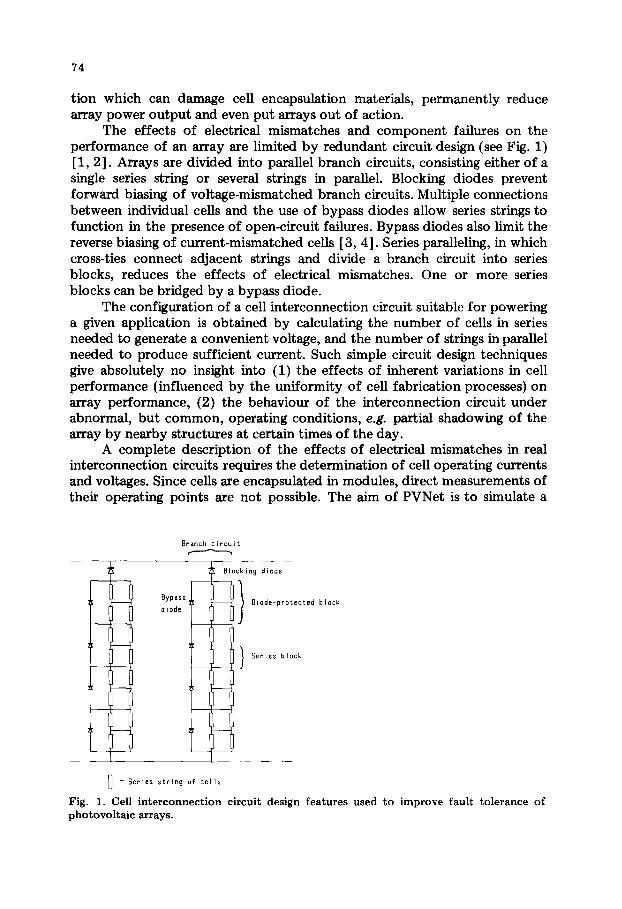
A complete description of the effects of electrical mismatches in real interconnection circuits requires the determination of cell operating currents and voltages. Since cells are encapsulated in modules, direct measurements of their operating points are not possible. The aim of PVNet is to simulate a
Branch circuit
Bypas~ diode
Blocking diode
I Diode-protected block
Series block
] = Series string of cells
Fig. 1. Cell interconneetion circuit design features used to improve fault tolerance of photovoltaic arrays.
75
solar cell interconnection circuit in which the operating conditions of every circuit element can be observed. PVNet achieves this by manipulating the current-voltage ( I -V) characteristics of each circuit element.
Once PVNet was able to reproduce the well-known effects of electrical mismatches in series strings (reduction of power output , and power dissipa- t ion in the mismatched elements [ 3 ]), it was used to investigate the behaviour of series-parallel and series-parallel-series circuits, which are less well under- stood.
2. Overview of PVNet
The electrical behaviour of a cell interconnection circuit is completely described by its I - V characteristic, which is the resultant of the I - V character- istics of each circuit element.
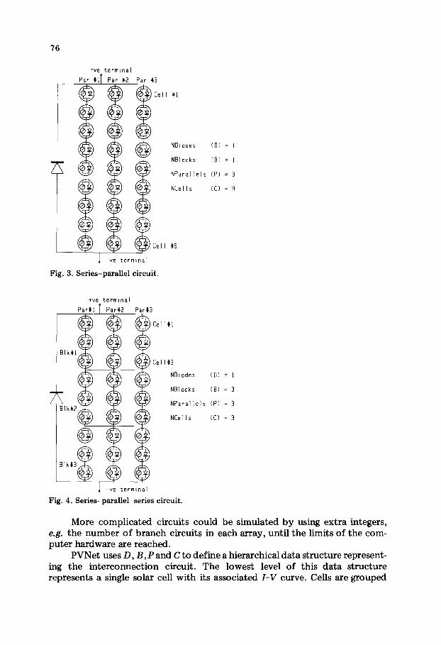
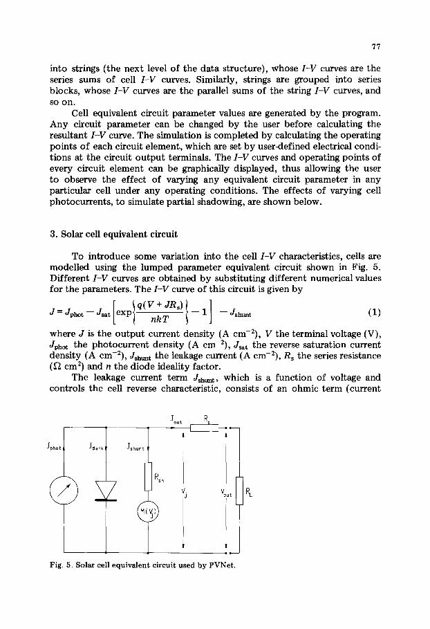
PVNet combines the I - V characteristics of circuit elements in series (summation of voltages) and in parallel (summation of currents) to obtain the resultant I - V curve of an interconnection circuit. Circuit elements are individual cells and bypass diodes, strings of cells, series blocks (groups of parallel-connected strings), diode-bypassed blocks (groups of series blocks bridged by a bypass diode) and complete branch circuits (see Fig. I) . Inter- connection circuits, up to the level of branch circuits, are defined by just four integers (see Figs. 2 - 4): ( I ) D, the number of bypass diodes in the circuit; (2) B, the number of series blocks bridged by each bypass diode; (3) P, the number of strings connected in parallel in each series block; (4) C, the number of cells connected in series in each string.
_ T +ve terminal
~Cell #l
NDiodes (D) = I
NBlocks (B) = I
NParaIIels (P) = !
NCeIls (C) = 10
• Cel] #18
I -ve terminal Fig. 2. Series string of cells bridged by a parallel bypass diode. The polarity of this connection should be noted.
76
+ve terminal
Par #i I Par #2
I - ve t e r m i n a l
Par #3 ~ Cel
NDiodes (D) = 1
NBIocks (B) = 1
N P a r a l l e l s (P) = 3
NCel ls (C) = B
Cell #9
Fig. 3. Series-parallel circuit.
+ve terminal Par#[ T Par~2 Par~3 C e l l # [
k# [
Ce11#3
NDiodes (D) = [
NBIocks (B) 3
N P a r a l l e l s (P) 3 k#2~ ~ ~ NCel ls (C) 3
I - re t e r m i n a l
Fig. 4. Series-parallel-series circuit.
More complicated circuits could be simulated by using extra integers, e.g. the number of branch circuits in each array, until the limits of the com- puter hardware are reached.
PVNet uses D, B, P and C to define a hierarchical data structure represent- ing the interconnection circuit. The lowest level of this data structure represents a single solar cell with its associated I - V curve. Cells are grouped
77
into strings (the next level of the data structure), whose I-V curves are the series sums of cell I-V curves. Similarly, strings are grouped into series blocks, whose I-V curves are the parallel sums of the string I-V curves, and so on.
Cell equivalent circuit parameter values are generated by the program. Any circuit parameter can be changed by the user before calculating the resultant I-V curve. The simulation is completed by calculating the operating points of each circuit element, which are set by user<lefined electrical condi- tions at the circuit ou tpu t terminals. The I-V curves and operating points of every circuit element can be graphically displayed, thus allowing the user to observe the effect of varying any equivalent circuit parameter in any particular cell under any operating conditions. The effects of varying cell photocurrents, to simulate partial shadowing, are shown below.
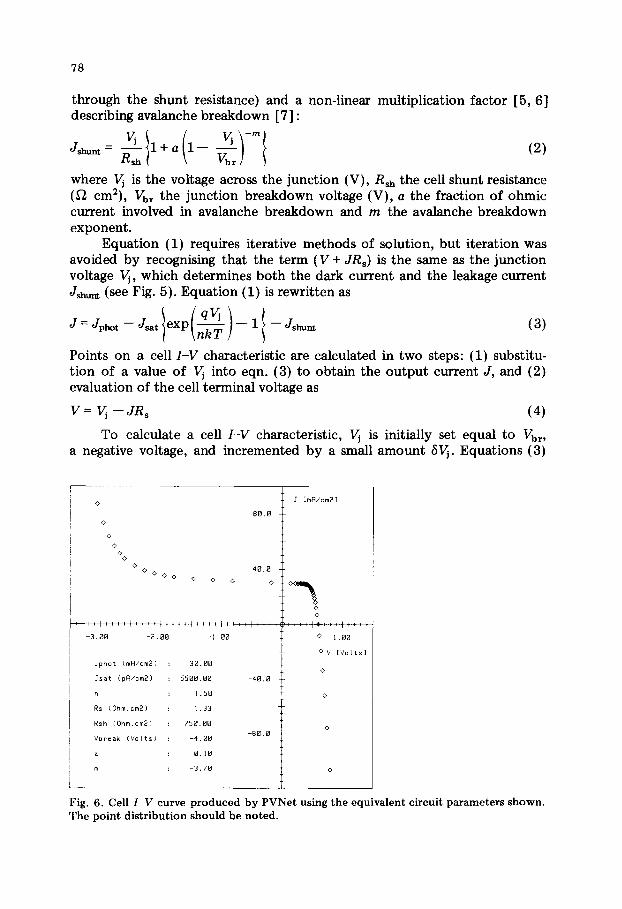
3. Solar cell equivalent circuit
To introduce some variation into the cell I-V characteristics, cells are modelled using the lumped parameter equivalent circuit shown in Fig. 5. Different I-V curves are obtained by substituting different numerical values for the parameters. The I-V curve of this circuit is given by
J = Jpk, t -- J~t l exPl q( V-~+kJRs) f --1 ] -- Jshunt (1)
where J is the ou tpu t current density (A cm-2), V the terminal voltage (V), J~ot the photocurrent density (A cm-2), Ju t the reverse saturation current density (A cm-2), J~h~t the leakage current (A cm-2), Rs the series resistance ( ~ cm 2) and n the diode ideality factor.
The leakage current term J~h~, which is a function of voltage and controls the cell reverse characteristic, consists of an ohmic term (current
Jphot| "Td ark I ]shunt Jout
J
Rsh
R
V V0u t
Fig. 5. Solar cell equivalent circuit used by PVNet.
R L
78
through the shunt resistance) and a non-linear multiplication factor [5, 6] describing avalanche breakdown [7] :
Jshu~ = ~ l + a 1-- Vbr / (2)
where V~ is the voltage across the junction (V), Rsh the cell shunt resistance (~2 cm2), Vbr the junction breakdown voltage (V), a the fraction of ohmic current involved in avalanche breakdown and m the avalanche breakdown exponent.
Equation (1) requires iterative methods of solution, but iteration was avoided by recognising that the term ( V + JRs) is the same as the junction voltage Vj, which determines both the dark current and the leakage current J ~ (see Fig. 5). Equation (1) is rewritten as
J = J p ~ t -- Jsat l e X P ( n ~ ) - - 1 f -- Js~at (3)
Points on a cell I - V characteristic are calculated in two steps: (1) substitu- tion of a value of V i into eqn. (3) to obtain the output current J, and (2) evaluation of the cell terminal voltage as
V = V i - - gRs (4)
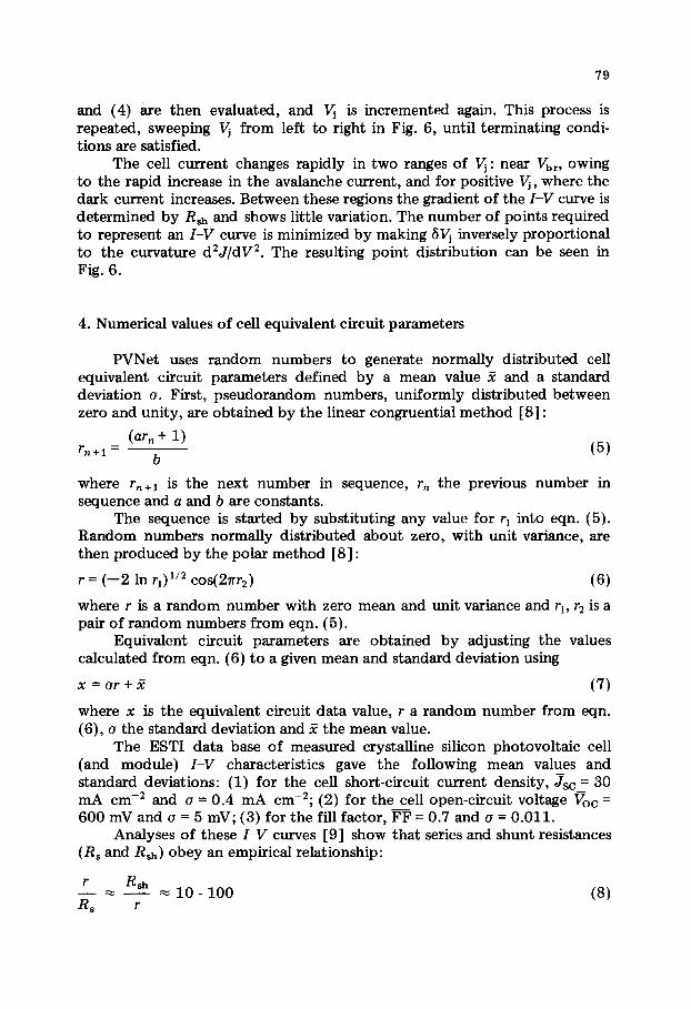
To calculate a cell I - V characteristic, V i is initially set equal to Vbr, a negative voltage, and incremented by a small amount ~iV i. Equations (3)
o
<>
o o
° o
80.0
40 .8 ~ O O O O
0 O O O
- 3 . 0 0 - 2 . 0 0 - ). 00
]phot (mR/cm2) : 3 0 . 0 0
] s a t ( pR /cm2) : 5 5 0 0 , 0 0 - 4 0 . 8
n ; 1 . 5 0
Rs (Ohm.cm2) : 1.33
Rsh (Ohm.cm2) : 750 .00
-BO.O Vbreak ( V o l t s ) : - 4 . 0 0
a : 8.1B
m : - 3 . 7 0
J [mR/cm2]
o
i . . . . i . . . .
o 1 . 0 0
0 V [ V o l t s ]
Fig. 6. Cell I - V curve produced by PVNet using the equivalent circuit parameters shown. The point distribution should be noted.
79
and (4) are then evaluated, and Vj is incremented again. This process is repeated, sweeping Vj from left to right in Fig. 6, until terminating condi- tions are satisfied.
The cell current changes rapidly in two ranges of Vj: near Vbr, owing to the rapid increase in the avalanche current, and for positive Vj, where the dark current increases. Between these regions the gradient of the I - V curve is determined by Rsh and shows little variation. The number of points required to represent an I - V curve is minimized by making 5Vj inversely proportional to the curvature d 2 J / d V 2. The resulting point distribution can be seen in Fig. 6.
4. Numerical values of cell equivalent circuit parameters
PVNet uses random numbers to generate normally distributed cell equivalent circuit parameters defined by a mean value ~ and a standard deviation o. First, pseudorandom numbers, uniformly distributed between zero and unity, are obtained by the linear congruential method [8] :
( a r . + 1) rn+ 1 = - (5)
b
where rn+l is the next number in sequence, r, the previous number in sequence and a and b are constants.
The sequence is started by substituting any value for rl into eqn. (5). Random numbers normally distributed about zero, with unit variance, are then produced by the polar method [8] :
r = (--2 In rl) 1/2 cos(27rr2) (6)
where r is a random number with zero mean and unit variance and rl, r2 is a pair of random numbers from eqn. (5).
Equivalent circuit parameters are obtained by adjusting the values calculated from eqn. (6) to a given mean and standard deviation using
x = o r + ~ (7)
where x is the equivalent circuit data value, r a random number from eqn. (6), a the standard deviation and ~ the mean value.
The ESTI data base of measured crystalline silicon photovoltaic cell (and module) I - V characteristics gave the following mean values and standard deviations: (1) for the cell short-circuit current density, Jsc = 30 mA cm -2 and o = 0.4 mA cm-2; (2) for the cell open-circuit voltage Voc = 600 mV and o = 5 mV; (3) for the fill factor, FF = 0.7 and o = 0.011.
Analyses of these I - V curves [9] show that series and shunt resistances (Rs and R~h) obey an empirical relationship:
r R~h - - ~ - - ~ 1 0 - 1 0 0 ( 8 ) Rs r
80
where r is t he o p t i m u m load resistance (equal to Vmp/Imp), Rs t he cell series resistance (~2) and Rsh the cell shunt resis tance (~2).
The fo l lowing mean and s tandard devia t ion values fo r equivalent circuit parameters were ob ta ined by trial and er ror and p ro d u ce I -V curves wi th short-circui t cu r ren t densities, open-c i rcui t voltages and fill fac tors falling wi thin the same ranges as the measured I -V curves: (1) fo r the p h o t o c u r r e n t densi ty , Jphot = 30.0 mA cm -2 and o = 0.4 mA cm-2; (2) fo r reverse satura- t ion cur ren t densi ty , J~at = 5.5 nA cm -2 and o = 0 .64 nA cm-2; (3) fo r the series resistance, R~ = 1.33 ~2 cm 2 and o = 0 .06 ~2 cm2; (4) fo r the shunt resistance, R~h = 750 [2 cm 2 and o = 100 ~ cm2; (5) fo r the reverse break- down voltage, 17br = - -15 .0 V and o = 3 V; (6) fo r the avalanche b r e a k d o w n expone n t , rfi = 3.7 and o = 0.1.
The values fo r the series and shunt resistances (R~ and R~h) and for the I-V curve m a x i m u m power cur ren ts and voltages (Imp and Vmp) o b e y eqn. (8). The mean and s tandard deviat ions of the avalanche b r e a k d o w n e x p o n e n t m were chosen to p roduce values o f m in the range 3.4 < m < 4, appropr ia te fo r avalanche b r e a k d o w n in silicon n+-p junc t ions [5] .
5. S u m m a t i o n o f I -V character is t ics
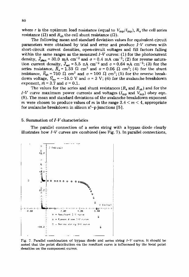
The parallel c o n n e c t i o n o f a series string wi th a bypass d iode clearly i l lustrates how I-V curves are c o m b i n e d (see Fig. 7). In parallel connec t ions ,
i.0 I
A 20.0 & &
I [mR/cm2]
A A
L ~ V ~Va;ts]
I 0 = Seri~s string I-V curve
Fig. 7. Parallel combination of bypass diode and series string I-V curves. It should be n o t e d t h a t t h e p o i n t d i s t r i b u t i o n o n t h e r e s u l t a n t c u r v e is i n f l u e n c e d b y t h e loca l p o i n t d e n s i t i e s o n t h e c o m p o n e n t cu rves .
81
the voltage across each element is the same; therefore the resultant I -V curve of a parallel circuit is obtained by summing the currents in each element at given voltages.
If bo th I -V curves were defined at the same voltages, the combination process would simply consist of algebraic summation of the currents. How- ever, I -V curves calculated using different equivalent circuit data have few common voltage values since (1) the initial value of Vj is the cell Vbr, (2) 5Vj varies during the calculation and (3) V depends on Rs through eqn. (4).
Current values at common voltages are therefore interpolated. The parallel combinat ion of two I -V curves is obtained by stepping through the curves, selecting voltage values from one to interpolate current values from the other.
The procedure for selecting interpolating voltages must consider the point densities in each I -V curve. This is clearly seen in Fig. 7 where each curve changes rapidly in a voltage range where the other curve is practically a straight line. Selecting voltage values from only one curve would result in the loss of most of the data describing the knee of the other curve. This is avoided by selecting interpolating voltage values from the curve with the higher local point density.
The process for combining two I -V curves in series is identical to that described above, except that current values are used to interpolate voltages.
6. Applications of PVNet
6.1. Mismatches in simple series circuits The first circuit to be simulated is the series string of ten cells shown in
Fig. 2. Cell operating points with the string operating at maximum power are shown in Fig. 8. For clarity, this plot only shows the knees of the cell I -V curves. Operating points are marked with a triangle, and maximum power points are marked with a diamond.
Cell operating points are set by the load across the string terminals. The series connection forces all cells to operate at the same current (the string maximum power current), and since the cell characteristics are slightly different, they operate at different voltages. This spread of operating points introduces mismatch losses, which reduce array performance [10].
As the load decreases, the string operating current rises. Eventually, the string current exceeds the lowest cell short-circuit current. Cells whose short- circuit currents are lower than the string current become reverse biased (see Fig. 9). This explains the observed temperature differences between cells in short-circuited modules. The power dissipated in a mismatched cell is determined by (1) the string operating point, as shown in Figs. 8 m~d 9, (2) the degree of mismatch and (3) the cell reverse characteristic.
Shadowing or cell damage cause much larger mismatches than inherent variations in cell performance. Large mismatches are simulated by reducing cell photocurrent densities. Figure 10 shows the I -V curves of a grossly

82
38.8
2 9 , 0
J EmA/om2)
= Operating Point
0 = Haximum Pouer Point
2 8 , 8 ~
26,0
25.0 0.48 0.47 8.48 8m4~ 8 m 58 O • 5 ~
Fig. 8. Spread of cell operating voltages in a series string generating maximum power. The series connection forces all cells to operate at the same current.
32.0
ili
I CmR/cm2]
= Operatin) Point
= Maximum Power Point
Y [Volts]
-8.48 -0°38 -8.20 -8.10 8.0B 8. t8 8.28 8.38 8.48 8,5~
Fig. 9. Cell operating points in a short-circuited series string. Cells with short-circuit currents lower than the string short-circuit current become reverse biased.
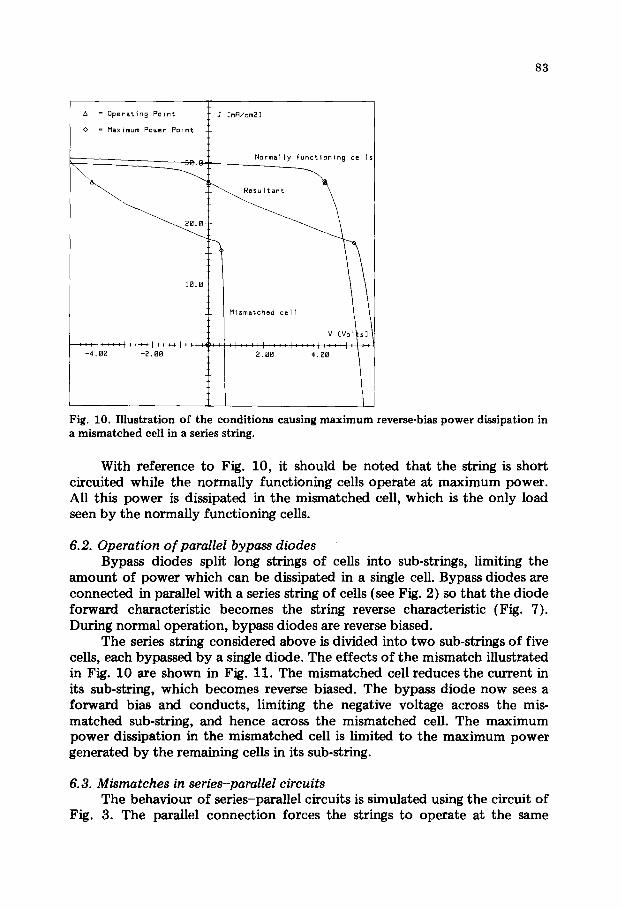
mismatched cell, o f the nine remaining normal ly funct ioning cells, and o f the w h o l e string (the resultant curve). The mismatched cell significantly degrades the string I-V curve. Large reduct ions in m a x i m u m power output have been observed in arrays containing damaged cells [ 11 ] .
83
= Operatin 9 Point
0 ~ Naximum Power Point
J [mR/cm2]
1 0 . 0 -
N o r m a l l y T u n c t i o n i n 9 c e l l s
\ Mlsmatched cell V [Vo s!
i I -4.0~ -2.eo 2.ao 4. ~z
Fig. 10. Illustration of the conditions causing maximum reverse-bias power a mismatched cell in a series string.
dissipation in
With reference to Fig. 10, it should be noted that the string is short circuited while the normally functioning cells operate at maximum power. All this power is dissipated in the mismatched cell, which is the only load seen by the normally functioning cells.
6.2. Operation o f parallel bypass diodes Bypass diodes split Ions[ strings of cells into sub-strings, limiting the
amount of power which can be dissipated in a single cell. Bypass diodes are connected in parallel with a series string of cells (see Fig. 2) so that the diode forward characteristic becomes the string reverse characteristic (Fig. 7). During normal operation, bypass diodes are reverse biased.
The series string considered above is divided into two sub-strings of five cells, each bypassed by a single diode. The effects of the mismatch illustrated in Fig. 10 are shown in Fig. 11. The mismatched cell reduces the current in its sub-string, which becomes reverse biased. The bypass diode now sees a forward bias and conducts, limiting the negative voltage across the mis- matched sub-string, and hence across the mismatched cell. The maximum power dissipation in the mismatched cell is limited to the maximum power generated by the remaining cells in its sub-string.
6. 3. Mismatches in series-parallel circuits The behaviour of series-parallel circuits is simulated using the circuit of
Fig. 3. The parallel connection forces the strings to operate at the same
84
l
[G 0
B,
. . . . J . . . . i , ,
3 [mR /cm2 ] 6 = Ope ra t i ng Po in t
0 = Max imum Power P~ in t
Normally ~unctioning sub-string
~ ~ Resu l t an t Mismatched sub-string 1
, , r i . . . . i . . . . I . . . . [ , , , . I , . , ~ . . . . ~ , , * , ~ . . . . I , l , I . . . . . . . . ~ V C V O ] t s ] . . . . i i . . . . . . . .
Fig. 11. I l lustrat ion of the reverse bias l imiting act ion of a parallel bypass diode.
voltage. When the circuit is shorted, the strings operate independently, generating their respective short-circuit currents. Current mismatches between cells in the same string produce the effects described above.
As the load is increased, the operating voltage of the circuit rises. When the operating voltage exceeds the lowest string open-circuit voltage, this string becomes forward biased and dissipates power. This process is illustrated in Fig. 12, which shows the I - V curves of one completely shadowed string, of the combination of the two normally operating strings, and of the series block, which is open circuited. The shadowed string is forward biased by the normally operating strings. Power is dissipated in every cell in the shadowed string.
If many parallel strings are present, as in an array, the forward charac- teristic of the mismatched string allows the current to increase practically wi thout limit, and this can cause destructive heating. This effect has been observed in large arrays (usually occurring when the edge of an array is shadowed by a neighbouring array either at sunrise or sunset) and is known as current imbalance [12].
Parallel bypass diodes, which limit reverse bias heating, provide no protection against current imbalance. During normal operation, bypass diodes are reverse biased, and remain so when the string itself is forward biased. To protect against current imbalance, it is necessary either to limit the number of parallel strings or to incorporate series blocking diodes in each string.

85
80.B I [mR/cm2] A = 0peratin 9 Point
O = Maximum Pouer Point
G8.0
4B.0 Normally-operating ~trings
20.8 Series-block
H , . . . . . . . . . . . . . . . . . . . .
. . . . , v E . '00 . . . . . . ~ 1 1 " ''6.0B . . . .
S h a d ° = e d = t r ~ ~ / -E0.0
-40.0
Fig. 12. Forward biasing of a shadowed string in an open-circuited series block.
6.4. Operation of series blocking diodes Blocking diodes, connected as shown in Fig. 1 modify the forward
characteristic of a string. In normal operation, the blocking diode is forward biased, and conducts the string current, introducing a small voltage drop (see Fig. 13). When the string operating voltage is exceeded by the circuit operat-
2 .0 -
;4.0--
Blo; ,ing dlcde
LO-
! :
I [mR/cm2] A = Operating Point
0 ffi Maximum Power Point
].8-
L . . . . . . . f
~~ er ies string
~ i ~ I R I I I I I I ~ V [Volts]
2 08 4 00
Fig. 13. Modif icat ion o f the I - V curve o f a series string by a series b locking diode.

8 6
ing voltage, the blocking diode becomes reverse biased, limiting the current flowing in the string to a negligible diode leakage current.
Apart from eliminating current imbalance, blocking diodes prevent battery sets, used to store excess energy generated by the array, from dis- charging through the array at night.
J [mR/cm2] ~ = Operating Point
0 = Maximum Po=er Point
10
N o r m a l l y o p o r a t i n g
g0.0 blocks
Nizmatched block R e s u l t a n t
60.0
4g.0
20.0
V [Vo l t ~ ]
- 2 . 0 0 0 . 0 0 2 ,00 4.00 6 . 0 0
Fig. 14 . Reverse biasing o f a mismatched series b lock in a short-c ircuited ser ies -para l l e l - series network.
j [ii~ mFl/cm2 ]
2B'0 i
24.0=
18.0~
8,0 i & = Oporat in B Po in t
0 - Maximum Pouer Point ] 4.0"
V [Volt=]
- - 4 . 0 0 - - 3 g 0 0 - - ~ . 0 0 -- I " 0 0 0 " 0 0 I " 0 0
Fig. 15. Operating po in t s o f all n ine cells in the mismatched series block. The cross-t ies distr ibute p o w e r diss ipat ion over several cells.
87
6. 5. Mismatches in series-parallel-series circuits Series-parallel-series circuits are simulated using the circuit of Fig. 4.
This circuit is analogous to a series string of three cells, where each cell is a series-parallel block.
The effects of reducing the photocurrent of one cell are illustrated in Figs. 14 and 15. As shown in Fig. 14, the mismatch lowers the current generated by one block, which, in order to pass the higher current generated by the remaining two blocks, is forced into reverse bias. This behaviour is identical to that of a series string of three cells. It should be noted that the reverse characteristic of the resultant curve in Fig. 14 is due to the bypass diode. The cross-ties distribute current over each string, causing seven out of the nine cells in the block to become reverse biased (see Fig. 15).
Power is dissipated in the minimum number of cells when one cell from each parallel string in the same block is mismatched. This effect was observed during module hot-spot endurance tests performed at the ESTI laboratory [7 ].
7. Discussion
Although it uses a simple lumped parameter equivalent circuit model of a solar cell, PVNet reproduces the observed behaviour of networks of solar cells. This is only achieved by considering all three quadrants of cell I -V characteristics. More realistic solar cell models could easily be used.
The program shows that power is dissipated inside an interconnection circuit when the operating conditions cause electrically mismatched elements to operate under forward or reverse bias. Power dissipation is greatest under abnormal operating conditions, i.e. when the ou tpu t terminals are short or open circuited. These conditions should therefore be avoided if the inter- connection circuit is not adequately protected with bypass and blocking diodes.
Forward bias power dissipation occurs in elements of a parallel connec- t ion whose open-circuit voltages are lower than the operating voltage of the circuit. Conversely, reverse bias power dissipation occurs in elements of a series connect ion whose short-circuit currents are lower than the operating current of the circuit.
Reverse b i a s power dissipation is the commonest cause of hot-spot heating in photovoltalc arrays, and is limited, bu t not prevented, by the use of parallel bypass diodes. Ideally, every cell would be bypassed by a diode fabricated on the cell itself [ 13 - 15]. This minimizes bo th the power dissipated in a mismatched cell, and the consequent reduction in array power output .
The alternative to using bypass diodes is t o control the shape of cell reverse characteristics, either by reducing cell shunt resistances [16] or by reducing junct ion breakdown voltages. Shunt resistances are kept as high as possible to improve I -V curve fill factors. However, a high shunt resistance in
88
a mismatched cell significantly reduces array power ou tpu t and concentrates power dissipation in that cell.
Reducing the shunt resistance is unacceptable, since curve fill factors are degraded. Control of cell junction breakdown voltages may therefore be the best way to produce cells with soft reverse characteristics.
8. Conclusions
The observed electrical behaviour of solar cell interconnection circuits has been simulated by a computer program. The mechanisms of hot-spot heating, and of protect ion against hot-spot heating, in series, series-parallel and series-parallel-series circuits have been explained. All three quadrants of the cell I - V characteristic must be considered to predict the behaviour of a network of solar cells.
The I - V curve combination routines could be used with measured data (e.g. module I - V characteristics) making it possible to predict the perfor- mance of a real installation. However, for evaluating the behaviour of different interconnection circuit configurations, the lumped parameter equivalent circuit model appears to be sufficiently accurate.
Electrical mismatches due to process-induced variations in cell perfor- mance, random shadowing and cell damage are inevitable in a real installation. Solar cells can therefore be expected to operate in the second or third quadrants of their I -V characteristics. The behaviour of solar cells under these conditions should be investigated.
References
1 C. C. Gonzalez and R. W. Weaver, Circuit design considerations for photovoltaic modules and arrays, Proc. 14th IEEE Photovoltaic Specialists' Conf., San Diego, CA, 1980, IEEE, New York, 1980, p. 528.
2 R. G. Ross, Photovoltaic module and array reliability, Proc. 15th IEEE Photovoltaic Specialists' Conf., Orlando, FL, 1981, IEEE, New York, 1981, p. 1157.
3 F. A. Blake and K. L. Hanson, The 'hot-spot ' failure mode for solar arrays, Proc. 4th Intersociety Energy Conversion Engineering Conf., 1969, p. 575.
4 N. F. Shephard and R. S. Sugimura, The integration of bypass diodes with terrestrial photovoltaic modules and arrays, Proc. 17th IEEE Photovoltaic Specialists' Conf., Kissimmee, FL, 1984, IEEE, New York, 1984, p. 676.
5 S. L. Miller, Ionisation rates for holes and electrons in silicon, Phys. Rev., 105 (1957) 1246.
6 R. A. Hartman, J. L. Prince and J. W. Lathrop, Second quadrant effects in silicon solar cells, Proc. 14th IEEE Photovoltaic Specialists' Conf., San Diego, CA, 1980, IEEE, New York, 1980, p. 119.
7 S. Pace, J. Bishop and M. Magni, Hot-spots in solar cells -- test procedures and study of related phenomena, Proc. 6th Commission o f the European Communities Conf. on Photovoltaic Solar Energy, London, 1986, Reidel, Dordrecht, 1986, p. 304.
8 D. E. Knuth, Art o f Computer Programming, Vol. 2, 3eminumerical Algorithms, Addison Wesley, New York, 1969.
89
9 H. A. Ossenbrink, Commission of the European Communities Joint Research Centre ESTI Project, unpublished data, 1985.
10 L. L. Bucciarelli, Power loss in photovoltaic arrays due to mismatch in cell character- istics, Sol. Energy, 23 (1979) 277.
11 S. E. Forman and M. P. Themelis, Performance and reliability of photovoltaic modules at various MIT LL test sites, Proc. 14th IEEE Photovoltaic Specialists' Conf., San Diego, CA, 1980, IEEE, New York, 1980, p. 1284.
12 C. C. Gonzalez, R. W. Weaver, R. G. Ross, R. Spencer and J. C. Arnett, Determination of hot-spot susceptibility of multistring photovoltaic modules in a central-station application, Proc. 17th IEEE Photovoltaic Specialists' Conf., Kissimmee, FL, 1984, IEEE, New York, 1984, p. 668.
13 C. H. Cox, D. J. Silversmith and R. W. Mountain, Reduction of photovoltaic cell reverse breakdown by a peripheral bypass diode, Proc. 16th IEEE Photovoltaic Specialists" Conf., San Diego, CA, 1982, IEEE, New York, 1982, p. 834.
14 M. A. Green, E. S. Hasyim, S. R. Wenham and M. R. Willison, Silicon solar cells with integral bypass diodes, Proc. 17th IEEE Photovoltaic Specialists' Conf., Kissimmee, FL, 1984, IEEE, New York, 1984, p. 513.
15 N. Mardesich and M. Gillanders, Integral diode solar cells, Proc. 17th IEEE Photo- voltaic Specialists' Conf., Kissimmee, FL, 1984, IEEE, New York, 1984, p. 196.
16 A. M. Ricaud, Solar cells failure modes and improvement of reverse characteristics, Proc. 4th Commission o f the European Communities Conf. on Photovoltaic Solar Energy, Stresa, 1982, Reidel, Dordrecht, 1982, p. 392.