Embed Size (px)
Citation preview

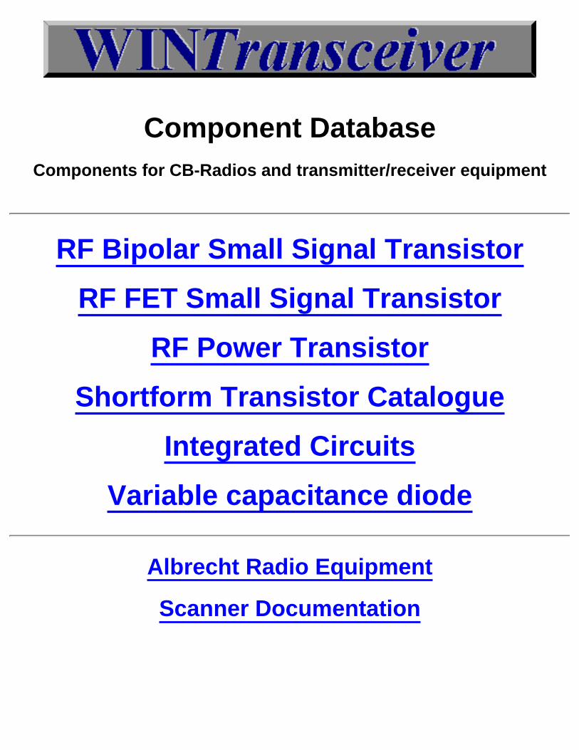
Component DatabaseComponents for CB-Radios and transmitter/receiver equipment
RF Bipolar Small Signal Transistor
RF FET Small Signal Transistor
RF Power Transistor
Shortform Transistor Catalogue
Integrated Circuits
Variable capacitance diode
Albrecht Radio Equipment
Scanner Documentation
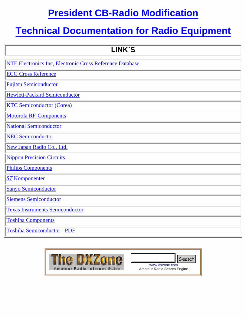
President CB-Radio Modification
Technical Documentation for Radio Equipment
LINK`S
NTE Electronics Inc, Electronic Cross Reference Database
ECG Cross Reference
Fujitsu Semiconductor
Hewlett-Packard Semiconductor
KTC Semiconductor (Corea)
Motorola RF-Components
National Semiconductor
NEC Semiconductor
New Japan Radio Co., Ltd.
Nippon Precision Circuits
Philips Components
ST Komponenter
Sanyo Semiconductor
Siemens Semiconductor
Texas Instruments Semiconductor
Toshiba Components
Toshiba Semiconductor - PDF
www.dxzone.comAmateur Radio Search Engine

CB Radio Banner Exchange
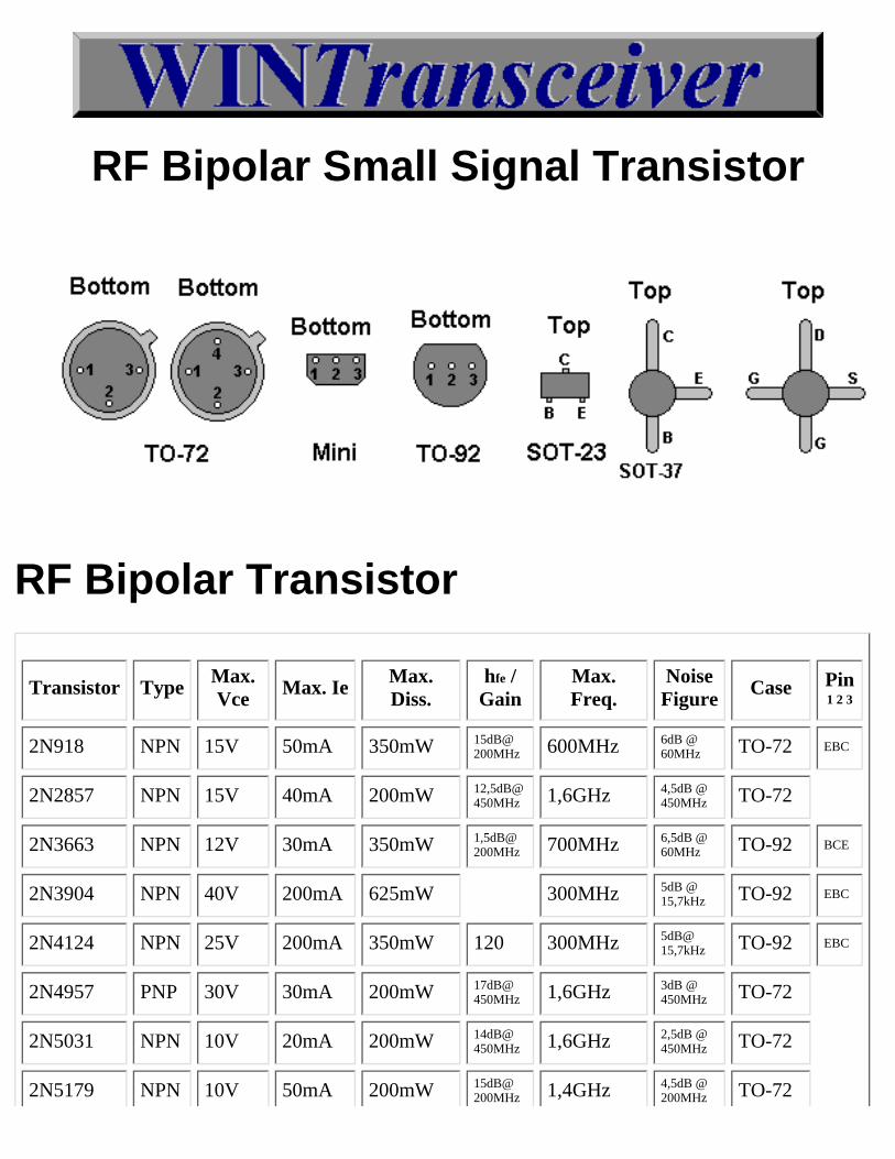
RF Bipolar Small Signal Transistor
RF Bipolar Transistor
Transistor Type Max.Vce Max. Ie Max.
Diss.hfe /
GainMax.Freq.
NoiseFigure Case Pin
1 2 3
2N918 NPN 15V 50mA 350mW 15dB@200MHz 600MHz 6dB @
60MHz TO-72 EBC
2N2857 NPN 15V 40mA 200mW 12,5dB@450MHz 1,6GHz 4,5dB @
450MHz TO-72
2N3663 NPN 12V 30mA 350mW 1,5dB@200MHz 700MHz 6,5dB @
60MHz TO-92 BCE
2N3904 NPN 40V 200mA 625mW 300MHz 5dB @15,7kHz TO-92 EBC
2N4124 NPN 25V 200mA 350mW 120 300MHz 5dB@15,7kHz TO-92 EBC
2N4957 PNP 30V 30mA 200mW 17dB@450MHz 1,6GHz 3dB @
450MHz TO-72
2N5031 NPN 10V 20mA 200mW 14dB@450MHz 1,6GHz 2,5dB @
450MHz TO-72
2N5179 NPN 10V 50mA 200mW 15dB@200MHz 1,4GHz 4,5dB @
200MHz TO-72
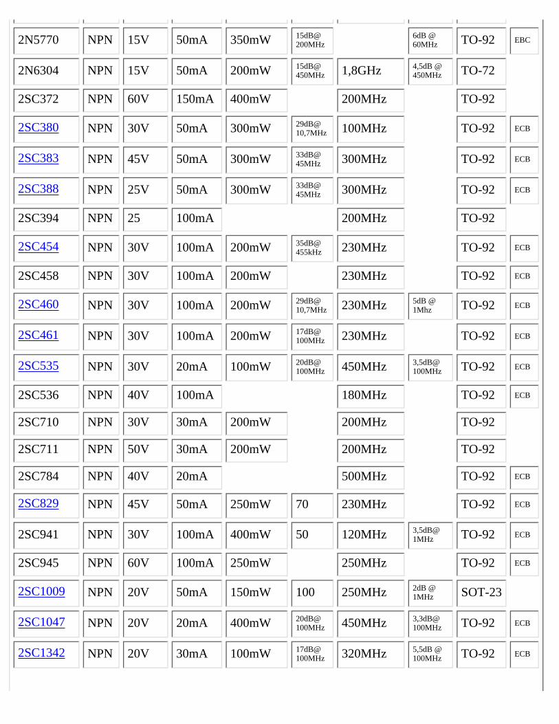
2N5770 NPN 15V 50mA 350mW 15dB@200MHz
6dB @60MHz TO-92 EBC
2N6304 NPN 15V 50mA 200mW 15dB@450MHz 1,8GHz 4,5dB @
450MHz TO-72
2SC372 NPN 60V 150mA 400mW 200MHz TO-92
2SC380 NPN 30V 50mA 300mW 29dB@10,7MHz 100MHz TO-92 ECB
2SC383 NPN 45V 50mA 300mW 33dB@45MHz 300MHz TO-92 ECB
2SC388 NPN 25V 50mA 300mW 33dB@45MHz 300MHz TO-92 ECB
2SC394 NPN 25 100mA 200MHz TO-92
2SC454 NPN 30V 100mA 200mW 35dB@455kHz 230MHz TO-92 ECB
2SC458 NPN 30V 100mA 200mW 230MHz TO-92 ECB
2SC460 NPN 30V 100mA 200mW 29dB@10,7MHz 230MHz 5dB @
1Mhz TO-92 ECB
2SC461 NPN 30V 100mA 200mW 17dB@100MHz 230MHz TO-92 ECB
2SC535 NPN 30V 20mA 100mW 20dB@100MHz 450MHz 3,5dB@
100MHz TO-92 ECB
2SC536 NPN 40V 100mA 180MHz TO-92 ECB
2SC710 NPN 30V 30mA 200mW 200MHz TO-92
2SC711 NPN 50V 30mA 200mW 200MHz TO-92
2SC784 NPN 40V 20mA 500MHz TO-92 ECB
2SC829 NPN 45V 50mA 250mW 70 230MHz TO-92 ECB
2SC941 NPN 30V 100mA 400mW 50 120MHz 3,5dB@1MHz TO-92 ECB
2SC945 NPN 60V 100mA 250mW 250MHz TO-92 ECB
2SC1009 NPN 20V 50mA 150mW 100 250MHz 2dB @1MHz SOT-23
2SC1047 NPN 20V 20mA 400mW 20dB@100MHz 450MHz 3,3dB@
100MHz TO-92 ECB
2SC1342 NPN 20V 30mA 100mW 17dB@100MHz 320MHz 5,5dB @
100MHz TO-92 ECB

2SC1674 NPN 30V 25mA 250mW 18dB@100MHz 600MHz 5dB@
100MHz TO-92 ECB
2SC1675 NPN 30V 30mA 250mW 40 150MHz 4dB @1MHz TO-92 ECB
2SC1730 NPN 30V 50mA 250mW 1,1GHz TO-92
2SC1815 NPN 40V 100mA 300mW 70 200MHz 1dB@1kHz TO-92 ECB
2SC1856 NPN 20V 20mA 250mW 200MHz TO-92
2SC1906 NPN 20V 50mA 300mW 33dB@45MHz 1GHz TO-92 ECB
2SC1907 NPN 20V 50mA 300mW 40 1,1GHz TO-92 ECB
2SC1923 NPN 30V 20mA 100mW 18dB@100MHz 550MHz 2,5dB@
100MHz TO-92 ECB
2SC2026 NPN 15V 50mA 2.2GHz TO-92 BEC
2SC2037 NPN 15V 50mA TO-92
2SC2120 NPN 30V 800mA 600mW 100 120MHz TO-92 ECB
2SC2216 NPN 45V 50mA 300mW 29dB@45MHz 300MHz TO-92 BEC
2SC2347 NPN 15V 50mA 250mW 20 650MHz TO-92 ECB
2SC2349 NPN 15V 50mA 250mW 600MHz TO-92 ECB
2SC2407 NPN 35V 150mA 600mW 500MHz TO-92
2SC2471 NPN 30V 50mA 310mW 20 2GHz TO-92 ECB
2SC2498 NPN 20V 50mA 300mW 80 3,5GHz 2,5dB @500MHz TO-92 BEC
2SC2512 NPN 20V 50mA 300mW 20dB@200MHz 900MHz 3,8dB @
200MHz TO-92 BEC
2SC2644 NPN 12V 120mA 500mW 18dB@100MHz 4GHz 2dB@
100MHz TO-92 BEC
2SC2668 NPN 30V 20mA 100mW 18dB@100MHz 550MHz 2,5dB@
100MHz MINI ECB
2SC2669 NPN 30V 50mA 200mW 30dB@10,7MHz 100MHz MINI ECB
2SC2717 NPN 25V 50mA 300mW 28dB@45MHz 300MHz TO-92 BEC
2SC2724 NPN 30V 25mA 250mW 600MHz TO-92 ECB
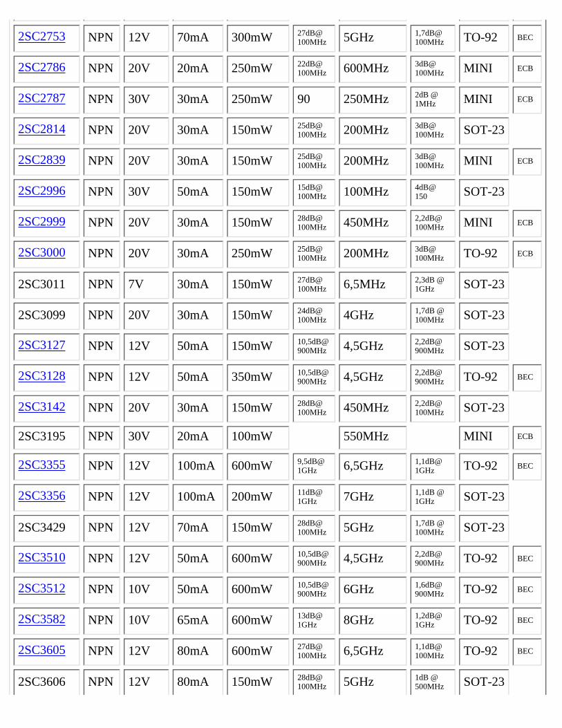
2SC2753 NPN 12V 70mA 300mW 27dB@100MHz 5GHz 1,7dB@
100MHz TO-92 BEC
2SC2786 NPN 20V 20mA 250mW 22dB@100MHz 600MHz 3dB@
100MHz MINI ECB
2SC2787 NPN 30V 30mA 250mW 90 250MHz 2dB @1MHz MINI ECB
2SC2814 NPN 20V 30mA 150mW 25dB@100MHz 200MHz 3dB@
100MHz SOT-23
2SC2839 NPN 20V 30mA 150mW 25dB@100MHz 200MHz 3dB@
100MHz MINI ECB
2SC2996 NPN 30V 50mA 150mW 15dB@100MHz 100MHz 4dB@
150 SOT-23
2SC2999 NPN 20V 30mA 150mW 28dB@100MHz 450MHz 2,2dB@
100MHz MINI ECB
2SC3000 NPN 20V 30mA 250mW 25dB@100MHz 200MHz 3dB@
100MHz TO-92 ECB
2SC3011 NPN 7V 30mA 150mW 27dB@100MHz 6,5MHz 2,3dB @
1GHz SOT-23
2SC3099 NPN 20V 30mA 150mW 24dB@100MHz 4GHz 1,7dB @
100MHz SOT-23
2SC3127 NPN 12V 50mA 150mW 10,5dB@900MHz 4,5GHz 2,2dB@
900MHz SOT-23
2SC3128 NPN 12V 50mA 350mW 10,5dB@900MHz 4,5GHz 2,2dB@
900MHz TO-92 BEC
2SC3142 NPN 20V 30mA 150mW 28dB@100MHz 450MHz 2,2dB@
100MHz SOT-23
2SC3195 NPN 30V 20mA 100mW 550MHz MINI ECB
2SC3355 NPN 12V 100mA 600mW 9,5dB@1GHz 6,5GHz 1,1dB@
1GHz TO-92 BEC
2SC3356 NPN 12V 100mA 200mW 11dB@1GHz 7GHz 1,1dB @
1GHz SOT-23
2SC3429 NPN 12V 70mA 150mW 28dB@100MHz 5GHz 1,7dB @
100MHz SOT-23
2SC3510 NPN 12V 50mA 600mW 10,5dB@900MHz 4,5GHz 2,2dB@
900MHz TO-92 BEC
2SC3512 NPN 10V 50mA 600mW 10,5dB@900MHz 6GHz 1,6dB@
900MHz TO-92 BEC
2SC3582 NPN 10V 65mA 600mW 13dB@1GHz 8GHz 1,2dB@
1GHz TO-92 BEC
2SC3605 NPN 12V 80mA 600mW 27dB@100MHz 6,5GHz 1,1dB@
100MHz TO-92 BEC
2SC3606 NPN 12V 80mA 150mW 28dB@100MHz 5GHz 1dB @
500MHz SOT-23
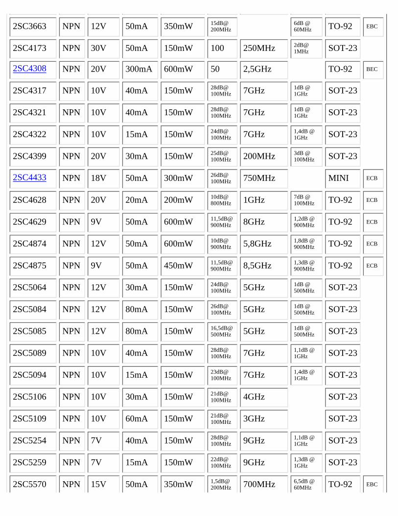
2SC3663 NPN 12V 50mA 350mW 15dB@200MHz
6dB @60MHz TO-92 EBC
2SC4173 NPN 30V 50mA 150mW 100 250MHz 2dB@1MHz SOT-23
2SC4308 NPN 20V 300mA 600mW 50 2,5GHz TO-92 BEC
2SC4317 NPN 10V 40mA 150mW 28dB@100MHz 7GHz 1dB @
1GHz SOT-23
2SC4321 NPN 10V 40mA 150mW 28dB@100MHz 7GHz 1dB @
1GHz SOT-23
2SC4322 NPN 10V 15mA 150mW 24dB@100MHz 7GHz 1,4dB @
1GHz SOT-23
2SC4399 NPN 20V 30mA 150mW 25dB@100MHz 200MHz 3dB @
100MHz SOT-23
2SC4433 NPN 18V 50mA 300mW 26dB@100MHz 750MHz MINI ECB
2SC4628 NPN 20V 20mA 200mW 10dB@800MHz 1GHz 7dB @
100MHz TO-92 ECB
2SC4629 NPN 9V 50mA 600mW 11,5dB@900MHz 8GHz 1,2dB @
900MHz TO-92 ECB
2SC4874 NPN 12V 50mA 600mW 10dB@900MHz 5,8GHz 1,8dB @
900MHz TO-92 ECB
2SC4875 NPN 9V 50mA 450mW 11,5dB@900MHz 8,5GHz 1,3dB @
900MHz TO-92 ECB
2SC5064 NPN 12V 30mA 150mW 24dB@100MHz 5GHz 1dB @
500MHz SOT-23
2SC5084 NPN 12V 80mA 150mW 26dB@100MHz 5GHz 1dB @
500MHz SOT-23
2SC5085 NPN 12V 80mA 150mW 16,5dB@500MHz 5GHz 1dB @
500MHz SOT-23
2SC5089 NPN 10V 40mA 150mW 28dB@100MHz 7GHz 1,1dB @
1GHz SOT-23
2SC5094 NPN 10V 15mA 150mW 23dB@100MHz 7GHz 1,4dB @
1GHz SOT-23
2SC5106 NPN 10V 30mA 150mW 21dB@100MHz 4GHz SOT-23
2SC5109 NPN 10V 60mA 150mW 21dB@100MHz 3GHz SOT-23
2SC5254 NPN 7V 40mA 150mW 28dB@100MHz 9GHz 1,1dB @
1GHz SOT-23
2SC5259 NPN 7V 15mA 150mW 22dB@100MHz 9GHz 1,3dB @
1GHz SOT-23
2SC5570 NPN 15V 50mA 350mW 1,5dB@200MHz 700MHz 6,5dB @
60MHz TO-92 EBC
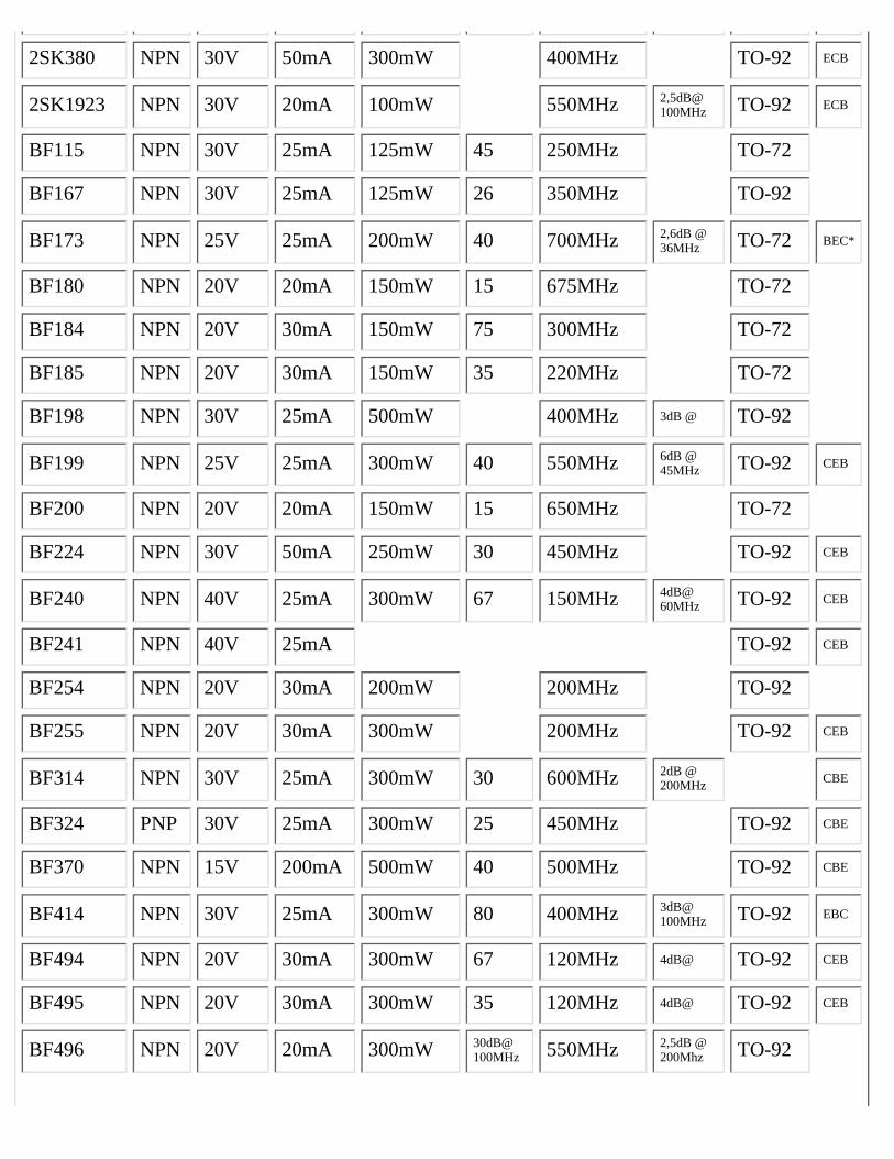
2SK380 NPN 30V 50mA 300mW 400MHz TO-92 ECB
2SK1923 NPN 30V 20mA 100mW 550MHz 2,5dB@100MHz TO-92 ECB
BF115 NPN 30V 25mA 125mW 45 250MHz TO-72
BF167 NPN 30V 25mA 125mW 26 350MHz TO-92
BF173 NPN 25V 25mA 200mW 40 700MHz 2,6dB @36MHz TO-72 BEC*
BF180 NPN 20V 20mA 150mW 15 675MHz TO-72
BF184 NPN 20V 30mA 150mW 75 300MHz TO-72
BF185 NPN 20V 30mA 150mW 35 220MHz TO-72
BF198 NPN 30V 25mA 500mW 400MHz 3dB @ TO-92
BF199 NPN 25V 25mA 300mW 40 550MHz 6dB @45MHz TO-92 CEB
BF200 NPN 20V 20mA 150mW 15 650MHz TO-72
BF224 NPN 30V 50mA 250mW 30 450MHz TO-92 CEB
BF240 NPN 40V 25mA 300mW 67 150MHz 4dB@60MHz TO-92 CEB
BF241 NPN 40V 25mA TO-92 CEB
BF254 NPN 20V 30mA 200mW 200MHz TO-92
BF255 NPN 20V 30mA 300mW 200MHz TO-92 CEB
BF314 NPN 30V 25mA 300mW 30 600MHz 2dB @200MHz CBE
BF324 PNP 30V 25mA 300mW 25 450MHz TO-92 CBE
BF370 NPN 15V 200mA 500mW 40 500MHz TO-92 CBE
BF414 NPN 30V 25mA 300mW 80 400MHz 3dB@100MHz TO-92 EBC
BF494 NPN 20V 30mA 300mW 67 120MHz 4dB@ TO-92 CEB
BF495 NPN 20V 30mA 300mW 35 120MHz 4dB@ TO-92 CEB
BF496 NPN 20V 20mA 300mW 30dB@100MHz 550MHz 2,5dB @
200Mhz TO-92

BF506 PNP 35V 30mA 300mW 17,5dB@200MHz 300MHz 3dB @
200Mhz TO-92 EBC
BF689K NPN 15V 25mA 360mW 16dB@200MHz 1,8GHz 3dB @
200Mhz TO-92
BF748 NPN 20V 50mA 500mW 20dB@100MHz 1,2GHz 4,5dB @
100Mhz TO-92
BF751 NPN 14V 35mA 600mW 11dB@1000MHz 6,5GHz 2,7dB @
1000Mhz TO-92
BF763 NPN 15V 25mA 360mW 13dB@800MHz 1,8GHz TO-92
BF775 NPN 15V 30mA 280mW 15dB@900MHz 5GHz 1,8dB @
900MHz SOT-23
BF799W NPN 20V 35mA 280mW 800MHz 3dB @100MHz SOT-23
BF840 NPN 40V 25mA 280mW 65 380MHz 1,7dB@100kHz SOT-23
BF926 NPN 20V 25mA 250mW 17,5dB@200MHz 350MHz 5dB @
200Mhz TO-92
BF959 NPN 20V 100mA 500mW 40 600MHz 3dB@200MHz TO-92
BFR90 NPN 15V 30mA 300mW 19,5dB@500MHz 5GHz 2,2dB @
500MHz SOT-37
BFR90A NPN 15V 30mA 300mW 16dB@800MHz 6GHz 2,8dB @
800MHz SOT-37
BFR91 NPN 12V 50mA 300mW 18dB@500MHz 5GHz 1,9dB @
500MHz SOT-37
BFR91A NPN 12V 50mA 300mW 14dB@800MHz 6GHz 1,6dB @
800MHz SOT-37
BFR92 NPN 15V 30mA 200mW 19,5dB@500MHz 5GHz 2,2dB @
500MHz SOT-23
BFR92A NPN 15V 30mA 200mW 16dB@800MHz 6GHz 1,8dB @
800MHz SOT-23
BFR92L NPN 15V 35mA 350mW 3,4GHz SOT-23
BFR93 NPN 12V 40mA 200mW 18dB@500MHz 5GHz 1,9dB@
500MHz SOT-23
BFR93A NPN 12V 40mA 200mW 14dB@800MHz 6GHz 1,6dB@
800MHz SOT-23
BFR93L NPN 12V 35mA 350mW 3GHz 2,5dB@30MHz SOT-23
BFR96 NPN 15V 100mA 500mW 14,5dB@500MHz 4,5GHz 2dB @
500MHz SOT-37
BFR96T NPN 15V 75mA 500mW 16dB@500MHz 5GHz 2,3dB@
500MHz SOT-23
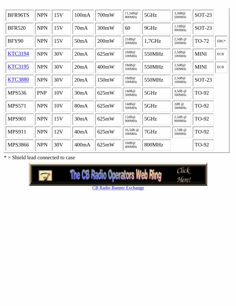
BFR96TS NPN 15V 100mA 700mW 11,5dB@800MHz 5GHz 3,3dB@
500MHz SOT-23
BFR520 NPN 15V 70mA 300mW 60 9GHz 1,1dB@900MHz SOT-23
BFY90 NPN 15V 50mA 200mW 21dB@200MHz 1,7GHz 2,5dB @
200MHz TO-72 EBC*
KTC3194 NPN 30V 20mA 625mW 18dB@100MHz 550MHz 2,5dB@
100MHz MINI ECB
KTC3195 NPN 30V 20mA 400mW 18dB@100MHz 550MHz 2,5dB@
100MHz MINI ECB
KTC3880 NPN 30V 20mA 150mW 18dB@100MHz 550MHz 2,5dB@
100MHz SOT-23
MPS536 PNP 10V 30mA 625mW 14dB@500MHz 5GHz 4,5dB @
500MHz TO-92
MPS571 NPN 10V 80mA 625mW 14dB@500MHz 5GHz 2dB @
500MHz TO-92
MPS901 NPN 15V 30mA 625mW 12dB@900MHz 5GHz 2,5dB @
900MHz TO-92
MPS911 NPN 12V 40mA 625mW 16,5dB @500MHz 7GHz 1,7dB @
500MHz TO-92
MPS3866 NPN 30V 400mA 625mW 10dB@400MHz 800MHz TO-92
* = Shield lead connected to case
CB Radio Banner Exchange
Component DatabaseComponents for CB-Radios and transmitter/receiver equipment
RF Bipolar Small Signal Transistor
RF FET Small Signal Transistor
RF Power Transistor
Shortform Transistor Catalogue
Integrated Circuits
Variable capacitance diode
Albrecht Radio Equipment
Scanner Documentation

President CB-Radio Modification
Technical Documentation for Radio Equipment
LINK`S
NTE Electronics Inc, Electronic Cross Reference Database
ECG Cross Reference
Fujitsu Semiconductor
Hewlett-Packard Semiconductor
KTC Semiconductor (Corea)
Motorola RF-Components
National Semiconductor
NEC Semiconductor
New Japan Radio Co., Ltd.
Nippon Precision Circuits
Philips Components
ST Komponenter
Sanyo Semiconductor
Siemens Semiconductor
Texas Instruments Semiconductor
Toshiba Components
Toshiba Semiconductor - PDF
www.dxzone.comAmateur Radio Search Engine

CB Radio Banner Exchange
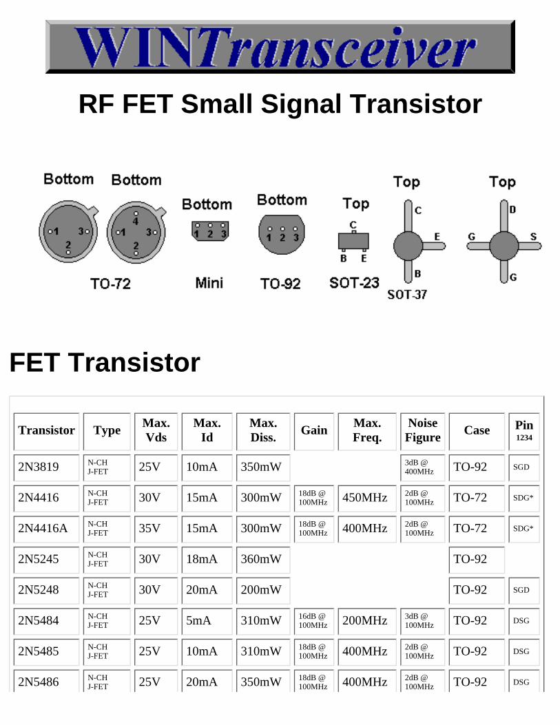
RF FET Small Signal Transistor
FET Transistor
Transistor Type Max.Vds
Max.Id
Max.Diss. Gain Max.
Freq.Noise
Figure Case Pin1234
2N3819 N-CHJ-FET 25V 10mA 350mW 3dB @
400MHz TO-92 SGD
2N4416 N-CHJ-FET 30V 15mA 300mW 18dB @
100MHz 450MHz 2dB @100MHz TO-72 SDG*
2N4416A N-CHJ-FET 35V 15mA 300mW 18dB @
100MHz 400MHz 2dB @100MHz TO-72 SDG*
2N5245 N-CHJ-FET 30V 18mA 360mW TO-92
2N5248 N-CHJ-FET 30V 20mA 200mW TO-92 SGD
2N5484 N-CHJ-FET 25V 5mA 310mW 16dB @
100MHz 200MHz 3dB @100MHz TO-92 DSG
2N5485 N-CHJ-FET 25V 10mA 310mW 18dB @
100MHz 400MHz 2dB @100MHz TO-92 DSG
2N5486 N-CHJ-FET 25V 20mA 350mW 18dB @
100MHz 400MHz 2dB @100MHz TO-92 DSG
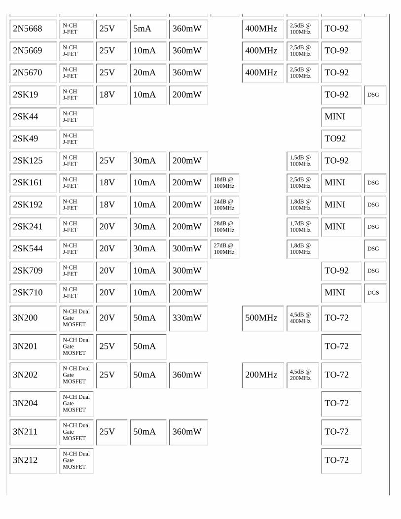
2N5668 N-CHJ-FET 25V 5mA 360mW 400MHz 2,5dB @
100MHz TO-92
2N5669 N-CHJ-FET 25V 10mA 360mW 400MHz 2,5dB @
100MHz TO-92
2N5670 N-CHJ-FET 25V 20mA 360mW 400MHz 2,5dB @
100MHz TO-92
2SK19 N-CHJ-FET 18V 10mA 200mW TO-92 DSG
2SK44 N-CHJ-FET MINI
2SK49 N-CHJ-FET TO92
2SK125 N-CHJ-FET 25V 30mA 200mW 1,5dB @
100MHz TO-92
2SK161 N-CHJ-FET 18V 10mA 200mW 18dB @
100MHz2,5dB @100MHz MINI DSG
2SK192 N-CHJ-FET 18V 10mA 200mW 24dB @
100MHz1,8dB @100MHz MINI DSG
2SK241 N-CHJ-FET 20V 30mA 200mW 28dB @
100MHz1,7dB @100MHz MINI DSG
2SK544 N-CHJ-FET 20V 30mA 300mW 27dB @
100MHz1,8dB @100MHz DSG
2SK709 N-CHJ-FET 20V 10mA 300mW TO-92 DSG
2SK710 N-CHJ-FET 20V 10mA 200mW MINI DGS
3N200N-CH DualGateMOSFET
20V 50mA 330mW 500MHz 4,5dB @400MHz TO-72
3N201N-CH DualGateMOSFET
25V 50mA TO-72
3N202N-CH DualGateMOSFET
25V 50mA 360mW 200MHz 4,5dB @200MHz TO-72
3N204N-CH DualGateMOSFET
TO-72
3N211N-CH DualGateMOSFET
25V 50mA 360mW TO-72
3N212N-CH DualGateMOSFET
TO-72

3N213N-CH DualGateMOSFET
TO-72
3SK39N-CH DualGateMOSFET
20V 25mA TO-72
3SK40N-CH DualGateMOSFET
15V 25mA 250mW TO-72
3SK45N-CH DualGateMOSFET
TO-72
3SK48N-CH DualGateMOSFET
TO-72
3SK51N-CH DualGateMOSFET
20V 35mA TO-72
3SK59N-CH DualGateMOSFET
20V 35mA TO-72
3SK72N-CH DualGateMOSFET
TO-72
3SK73N-CH DualGateMOSFET
20V 3mA TO-72
3SK74N-CH DualGateMOSFET
20V 7mA 200mW SOT-37
3SK75N-CH DualGateMOSFET
TO-72
3SK81N-CH DualGateMOSFET
20V 5mA
3SK88N-CH DualGateMOSFET
SOT-37
3SK97N-CH DualGateMOSFET
3SK126N-CH DualGateMOSFET
15V 30mA 150mW 25dB@200MHz
1,4dB@200MHz SOT-143 SDGG
3SK173N-CH DualGateMOSFET
TO-72
3SK180N-CH DualGateMOSFET
15V 30mA 200mW 28dB@100MHz
1,8dB@100MHz SOT-143 SDGG
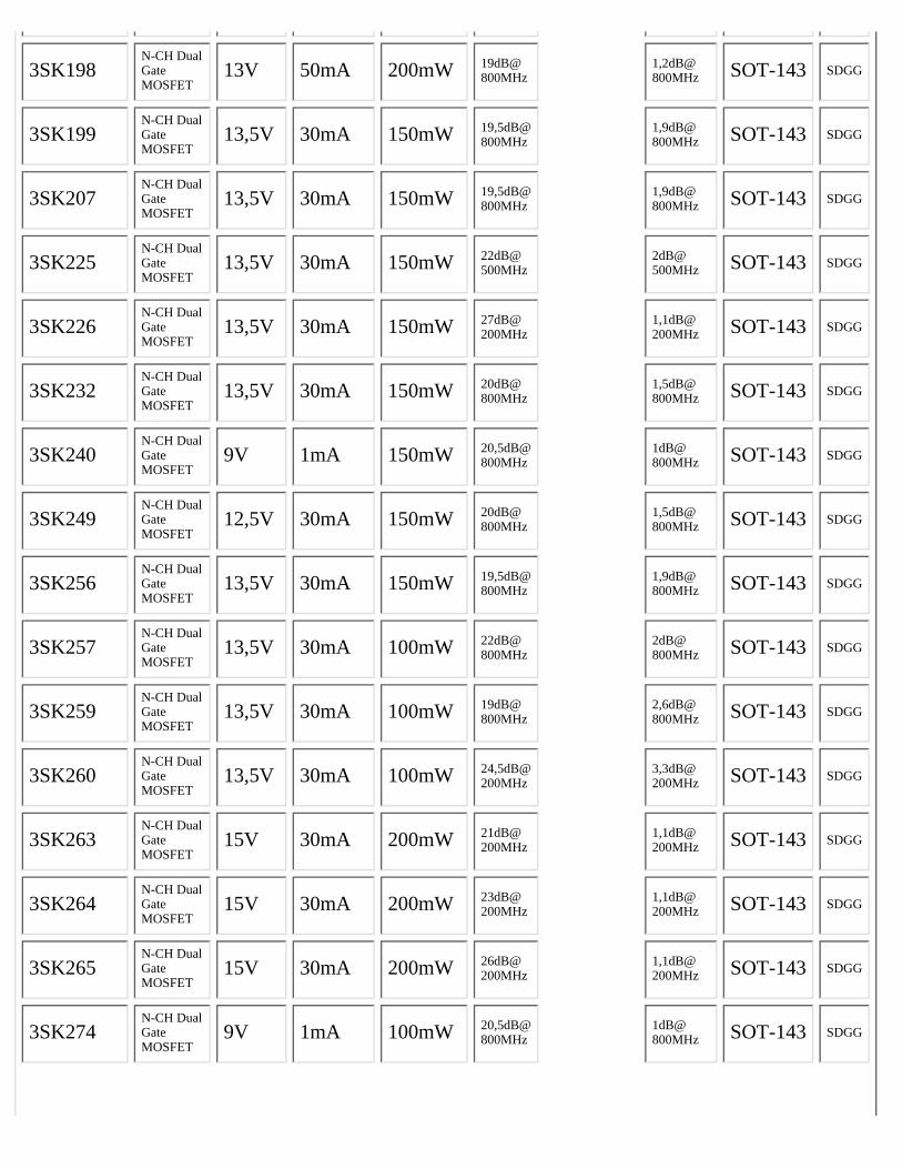
3SK198N-CH DualGateMOSFET
13V 50mA 200mW 19dB@800MHz
1,2dB@800MHz SOT-143 SDGG
3SK199N-CH DualGateMOSFET
13,5V 30mA 150mW 19,5dB@800MHz
1,9dB@800MHz SOT-143 SDGG
3SK207N-CH DualGateMOSFET
13,5V 30mA 150mW 19,5dB@800MHz
1,9dB@800MHz SOT-143 SDGG
3SK225N-CH DualGateMOSFET
13,5V 30mA 150mW 22dB@500MHz
2dB@500MHz SOT-143 SDGG
3SK226N-CH DualGateMOSFET
13,5V 30mA 150mW 27dB@200MHz
1,1dB@200MHz SOT-143 SDGG
3SK232N-CH DualGateMOSFET
13,5V 30mA 150mW 20dB@800MHz
1,5dB@800MHz SOT-143 SDGG
3SK240N-CH DualGateMOSFET
9V 1mA 150mW 20,5dB@800MHz
1dB@800MHz SOT-143 SDGG
3SK249N-CH DualGateMOSFET
12,5V 30mA 150mW 20dB@800MHz
1,5dB@800MHz SOT-143 SDGG
3SK256N-CH DualGateMOSFET
13,5V 30mA 150mW 19,5dB@800MHz
1,9dB@800MHz SOT-143 SDGG
3SK257N-CH DualGateMOSFET
13,5V 30mA 100mW 22dB@800MHz
2dB@800MHz SOT-143 SDGG
3SK259N-CH DualGateMOSFET
13,5V 30mA 100mW 19dB@800MHz
2,6dB@800MHz SOT-143 SDGG
3SK260N-CH DualGateMOSFET
13,5V 30mA 100mW 24,5dB@200MHz
3,3dB@200MHz SOT-143 SDGG
3SK263N-CH DualGateMOSFET
15V 30mA 200mW 21dB@200MHz
1,1dB@200MHz SOT-143 SDGG
3SK264N-CH DualGateMOSFET
15V 30mA 200mW 23dB@200MHz
1,1dB@200MHz SOT-143 SDGG
3SK265N-CH DualGateMOSFET
15V 30mA 200mW 26dB@200MHz
1,1dB@200MHz SOT-143 SDGG
3SK274N-CH DualGateMOSFET
9V 1mA 100mW 20,5dB@800MHz
1dB@800MHz SOT-143 SDGG
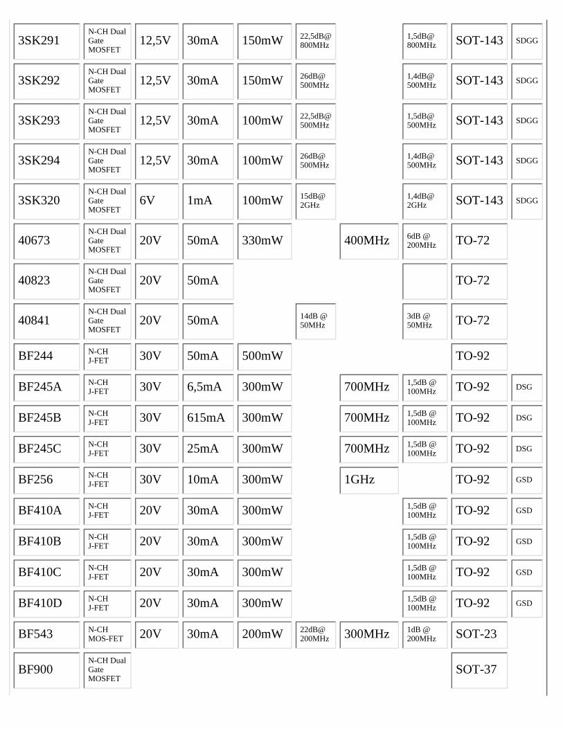
3SK291N-CH DualGateMOSFET
12,5V 30mA 150mW 22,5dB@800MHz
1,5dB@800MHz SOT-143 SDGG
3SK292N-CH DualGateMOSFET
12,5V 30mA 150mW 26dB@500MHz
1,4dB@500MHz SOT-143 SDGG
3SK293N-CH DualGateMOSFET
12,5V 30mA 100mW 22,5dB@500MHz
1,5dB@500MHz SOT-143 SDGG
3SK294N-CH DualGateMOSFET
12,5V 30mA 100mW 26dB@500MHz
1,4dB@500MHz SOT-143 SDGG
3SK320N-CH DualGateMOSFET
6V 1mA 100mW 15dB@2GHz
1,4dB@2GHz SOT-143 SDGG
40673N-CH DualGateMOSFET
20V 50mA 330mW 400MHz 6dB @200MHz TO-72
40823N-CH DualGateMOSFET
20V 50mA TO-72
40841N-CH DualGateMOSFET
20V 50mA 14dB @50MHz
3dB @50MHz TO-72
BF244 N-CHJ-FET 30V 50mA 500mW TO-92
BF245A N-CHJ-FET 30V 6,5mA 300mW 700MHz 1,5dB @
100MHz TO-92 DSG
BF245B N-CHJ-FET 30V 615mA 300mW 700MHz 1,5dB @
100MHz TO-92 DSG
BF245C N-CHJ-FET 30V 25mA 300mW 700MHz 1,5dB @
100MHz TO-92 DSG
BF256 N-CHJ-FET 30V 10mA 300mW 1GHz TO-92 GSD
BF410A N-CHJ-FET 20V 30mA 300mW 1,5dB @
100MHz TO-92 GSD
BF410B N-CHJ-FET 20V 30mA 300mW 1,5dB @
100MHz TO-92 GSD
BF410C N-CHJ-FET 20V 30mA 300mW 1,5dB @
100MHz TO-92 GSD
BF410D N-CHJ-FET 20V 30mA 300mW 1,5dB @
100MHz TO-92 GSD
BF543 N-CHMOS-FET 20V 30mA 200mW 22dB@
200MHz 300MHz 1dB @200MHz SOT-23
BF900N-CH DualGateMOSFET
SOT-37
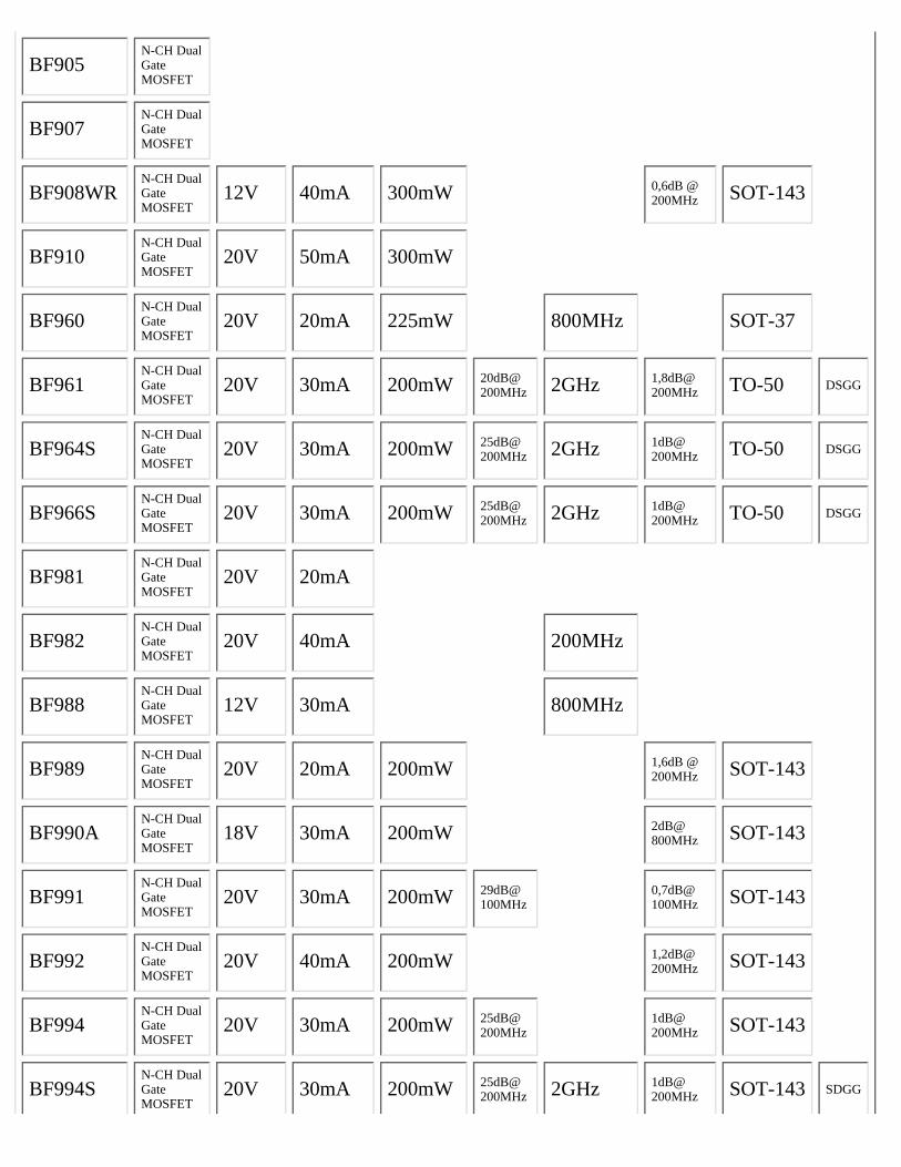
BF905N-CH DualGateMOSFET
BF907N-CH DualGateMOSFET
BF908WRN-CH DualGateMOSFET
12V 40mA 300mW 0,6dB @200MHz SOT-143
BF910N-CH DualGateMOSFET
20V 50mA 300mW
BF960N-CH DualGateMOSFET
20V 20mA 225mW 800MHz SOT-37
BF961N-CH DualGateMOSFET
20V 30mA 200mW 20dB@200MHz 2GHz 1,8dB@
200MHz TO-50 DSGG
BF964SN-CH DualGateMOSFET
20V 30mA 200mW 25dB@200MHz 2GHz 1dB@
200MHz TO-50 DSGG
BF966SN-CH DualGateMOSFET
20V 30mA 200mW 25dB@200MHz 2GHz 1dB@
200MHz TO-50 DSGG
BF981N-CH DualGateMOSFET
20V 20mA
BF982N-CH DualGateMOSFET
20V 40mA 200MHz
BF988N-CH DualGateMOSFET
12V 30mA 800MHz
BF989N-CH DualGateMOSFET
20V 20mA 200mW 1,6dB @200MHz SOT-143
BF990AN-CH DualGateMOSFET
18V 30mA 200mW 2dB@800MHz SOT-143
BF991N-CH DualGateMOSFET
20V 30mA 200mW 29dB@100MHz
0,7dB@100MHz SOT-143
BF992N-CH DualGateMOSFET
20V 40mA 200mW 1,2dB@200MHz SOT-143
BF994N-CH DualGateMOSFET
20V 30mA 200mW 25dB@200MHz
1dB@200MHz SOT-143
BF994SN-CH DualGateMOSFET
20V 30mA 200mW 25dB@200MHz 2GHz 1dB@
200MHz SOT-143 SDGG

BF995N-CH DualGateMOSFET
20V 30mA 200mW 20dB@200MHz
1,8dB@200MHz SOT-143 SDGG
BF996N-CH DualGateMOSFET
20V 30mA 200mW 25dB@200MHz
1dB@200MHz SOT-143
BF996SN-CH DualGateMOSFET
20V 30mA 200mW 25dB@200MHz 2GHz 1dB@
200MHz SOT-143 SDGG
BF997N-CH DualGateMOSFET
20V 30mA 200mW 25dB@200MHz 1GHz 1dB@
200MHz SOT-143
BF961N-CH DualGateMOSFET
20V 30mA 200mW 28dB@200MHz 2GHz 1dB@
200MHz SOT-143 SDGG
BF543 N-CHMOS-FET 20V 30mA 200mW 25dB@
200MHz 300MHz 1dB @200MHz SOT-23
BF1100N-CH DualGateMOSFET
14V 30mA 280mW 2dB@800MHz SOT-143
MFE201N-CH DualGateMOSFET
TO-72
MPF102 N-CHJ-FET 25V 20mA 310mW 200MHz 4dB @
400MHz TO-92
MPF106 N-CHJ-FET 25V 30mA 310mW 400MHz 4dB @
200MHz TO-92
SK3050N-CH DualGateMOSFET
20V 50mA 330mW 400MHz 6dB @200MHz TO-72
SK3065N-CH DualGateMOSFET
20V 50mA 330mW 500MHz 4,5dB @400MHz TO-72
SK3991N-CH DualGateMOSFET
25V 50mA 360mW 200MHz 4,5dB @200MHz TO-72
* = Shield lead connected to case
CB Radio Banner Exchange
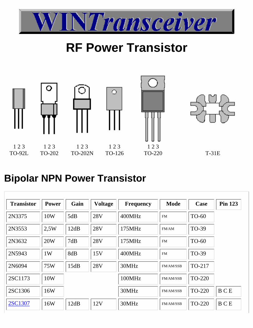
RF Power Transistor
1 2 3TO-92L
1 2 3TO-202
1 2 3TO-202N
1 2 3TO-126
1 2 3TO-220 T-31E
Bipolar NPN Power Transistor
Transistor Power Gain Voltage Frequency Mode Case Pin 123
2N3375 10W 5dB 28V 400MHz FM TO-60
2N3553 2,5W 12dB 28V 175MHz FM/AM TO-39
2N3632 20W 7dB 28V 175MHz FM TO-60
2N5943 1W 8dB 15V 400MHz FM TO-39
2N6094 75W 15dB 28V 30MHz FM/AM/SSB TO-217
2SC1173 10W 100MHz FM/AM/SSB TO-220
2SC1306 16W 30MHz FM/AM/SSB TO-220 B C E
2SC1307 16W 12dB 12V 30MHz FM/AM/SSB TO-220 B C E
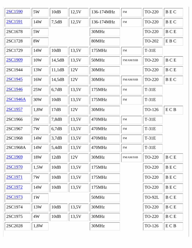
2SC1590 5W 10dB 12,5V 136-174MHz FM TO-220 B E C
2SC1591 14W 7,5dB 12,5V 136-174MHz FM TO-220 B E C
2SC1678 5W 30MHz TO-220 B C E
2SC1728 8W 80MHz TO-202 E B C
2SC1729 14W 10dB 13,5V 175MHz FM T-31E
2SC1909 10W 14,5dB 13,5V 50MHz FM/AM/SSB TO-220 B C E
2SC1944 13W 11,1dB 12V 30MHz TO-220 B C E
2SC1945 16W 14,5dB 12V 30MHz FM/AM/SSB TO-220 B E C
2SC1946 25W 6,7dB 13,5V 175MHz FM T-31E
2SC1946A 30W 10dB 13,5V 175MHz FM T-31E
2SC1957 1,8W 17dB 12V 30MHz TO-126 E C B
2SC1966 3W 7,8dB 13,5V 470MHz FM T-31E
2SC1967 7W 6,7dB 13,5V 470MHz FM T-31E
2SC1968 14W 3,7dB 13,5V 470MHz FM T-31E
2SC1968A 14W 5,4dB 13,5V 470MHz FM T-31E
2SC1969 18W 12dB 12V 30MHz FM/AM/SSB TO-220 B C E
2SC1970 1,5W 10dB 13,5V 175MHz TO-220 B E C
2SC1971 7W 10dB 13,5V 175MHz TO-220 B E C
2SC1972 14W 10dB 13,5V 175MHz TO-220 B E C
2SC1973 1W 50MHz TO-92L B C E
2SC1974 13W 10dB 13,5V 30MHz TO-220 B C E
2SC1975 4W 10dB 13,5V 30MHz TO-220 B C E
2SC2028 1,8W 30MHz TO-126 E C B
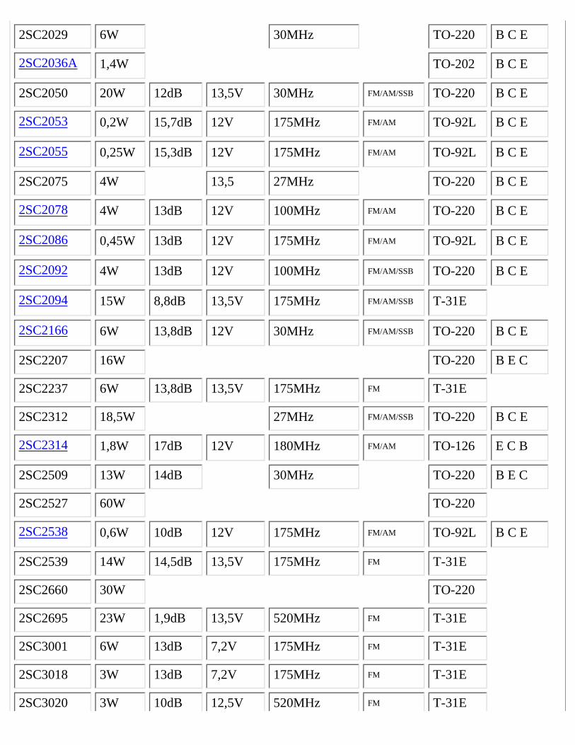
2SC2029 6W 30MHz TO-220 B C E
2SC2036A 1,4W TO-202 B C E
2SC2050 20W 12dB 13,5V 30MHz FM/AM/SSB TO-220 B C E
2SC2053 0,2W 15,7dB 12V 175MHz FM/AM TO-92L B C E
2SC2055 0,25W 15,3dB 12V 175MHz FM/AM TO-92L B C E
2SC2075 4W 13,5 27MHz TO-220 B C E
2SC2078 4W 13dB 12V 100MHz FM/AM TO-220 B C E
2SC2086 0,45W 13dB 12V 175MHz FM/AM TO-92L B C E
2SC2092 4W 13dB 12V 100MHz FM/AM/SSB TO-220 B C E
2SC2094 15W 8,8dB 13,5V 175MHz FM/AM/SSB T-31E
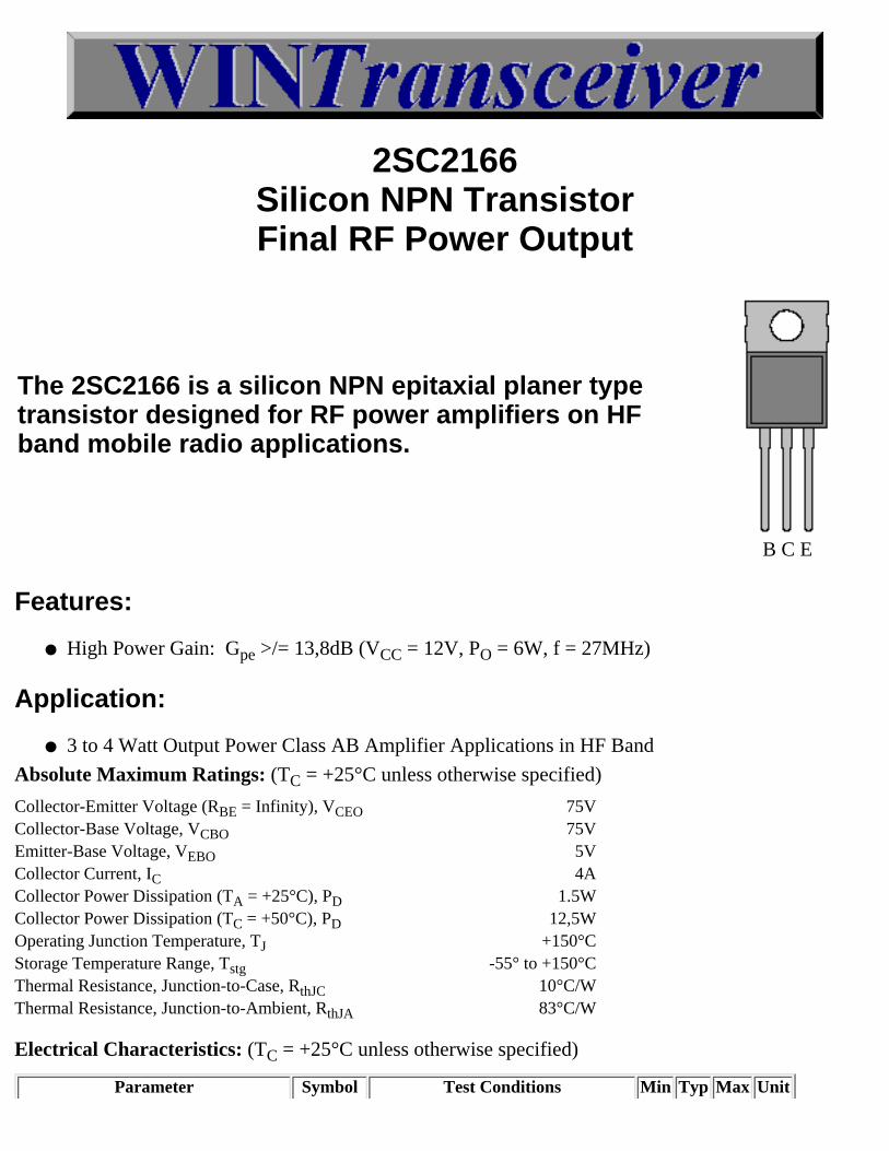
2SC2166 6W 13,8dB 12V 30MHz FM/AM/SSB TO-220 B C E
2SC2207 16W TO-220 B E C
2SC2237 6W 13,8dB 13,5V 175MHz FM T-31E
2SC2312 18,5W 27MHz FM/AM/SSB TO-220 B C E
2SC2314 1,8W 17dB 12V 180MHz FM/AM TO-126 E C B
2SC2509 13W 14dB 30MHz TO-220 B E C
2SC2527 60W TO-220
2SC2538 0,6W 10dB 12V 175MHz FM/AM TO-92L B C E
2SC2539 14W 14,5dB 13,5V 175MHz FM T-31E
2SC2660 30W TO-220
2SC2695 23W 1,9dB 13,5V 520MHz FM T-31E
2SC3001 6W 13dB 7,2V 175MHz FM T-31E
2SC3018 3W 13dB 7,2V 175MHz FM T-31E
2SC3020 3W 10dB 12,5V 520MHz FM T-31E
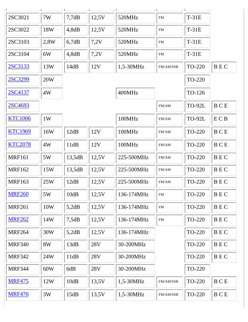
2SC3021 7W 7,7dB 12,5V 520MHz FM T-31E
2SC3022 18W 4,8dB 12,5V 520MHz FM T-31E
2SC3103 2,8W 6,7dB 7,2V 520MHz FM T-31E
2SC3104 6W 4,8dB 7,2V 520MHz FM T-31E
2SC3133 13W 14dB 12V 1,5-30MHz FM/AM/SSB TO-220 B E C
2SC3299 20W TO-220
2SC4137 4W 400MHz TO-126
2SC4693 FM/AM TO-92L B C E
KTC1006 1W 100MHz FM/AM TO-92L E C B
KTC1969 16W 12dB 12V 100MHz FM/AM TO-220 B C E
KTC2078 4W 11dB 12V 100MHz FM/AM TO-220 B C E
MRF161 5W 13,5dB 12,5V 225-500MHz FM/AM TO-220 B E C
MRF162 15W 13,5dB 12,5V 225-500MHz FM/AM TO-220 B E C
MRF163 25W 12dB 12,5V 225-500MHz FM/AM TO-220 B E C
MRF260 5W 10dB 12,5V 136-174MHz FM TO-220 B E C
MRF261 10W 5,2dB 12,5V 136-174MHz FM TO-220 B E C
MRF262 14W 7,5dB 12,5V 136-174MHz FM TO-220 B E C
MRF264 30W 5,2dB 12,5V 136-174MHz TO-220 B E C
MRF340 8W 13dB 28V 30-200MHz TO-220 B E C
MRF342 24W 11dB 28V 30-200MHz TO-220 B E C
MRF344 60W 6dB 28V 30-200MHz TO-220
MRF475 12W 10dB 13,5V 1,5-30MHz FM/AM/SSB TO-220 B C E
MRF476 3W 15dB 13,5V 1,5-30MHz FM/AM/SSB TO-220 B C E
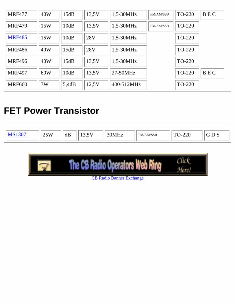
MRF477 40W 15dB 13,5V 1,5-30MHz FM/AM/SSB TO-220 B E C
MRF479 15W 10dB 13,5V 1,5-30MHz FM/AM/SSB TO-220
MRF485 15W 10dB 28V 1,5-30MHz TO-220
MRF486 40W 15dB 28V 1,5-30MHz TO-220
MRF496 40W 15dB 13,5V 1,5-30MHz TO-220
MRF497 60W 10dB 13,5V 27-50MHz TO-220 B E C
MRF660 7W 5,4dB 12,5V 400-512MHz TO-220
FET Power Transistor
MS1307 25W dB 13,5V 30MHz FM/AM/SSB TO-220 G D S
CB Radio Banner Exchange

2SC1307Silicon NPN TransistorFinal RF Power Output
The 2SC1307 is a silicon NPN epitaxial planer typetransistor designed for RF power amplifiers on HFband mobile radio applications.
B C E
Features:
High Power Gain: Gpe >/= 12dB (VCC = 12V, PO = 16W, f = 27MHz)●
Ability to Withstand Infinite VSWR Load when Operated at: VCC = 16V, PO = 20W, f = 27MHz
●
Application:
10 to 14 Watt Output Power Class AB Amplifier Applications in HF Band●
Absolute Maximum Ratings: (TC = +25°C unless otherwise specified)
Collector-Emitter Voltage (RBE = Infinity), VCEO 25VCollector-Base Voltage, VCBO 60VEmitter-Base Voltage, VEBO 5VCollector Current, IC 6ACollector Power Dissipation (TA = +25°C), PD 1.7WCollector Power Dissipation (TC = +50°C), PD 20WOperating Junction Temperature, TJ +150°CStorage Temperature Range, Tstg -55° to +150°CThermal Resistance, Junction-to-Case, RthJC 6.25°C/WThermal Resistance, Junction-to-Ambient, RthJA 73.5°C/W

Electrical Characteristics: (TC = +25°C unless otherwise specified)
Parameter Symbol Test Conditions Min Typ Max Unit
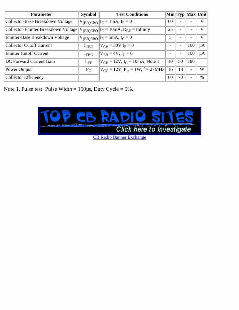
Collector-Base Breakdown Voltage V(BR)CBO IC = 1mA, IE = 0 60 - - V
Collector-Emitter Breakdown Voltage V(BR)CEO IC = 10mA, RBE = Infinity 25 - - V
Emitter-Base Breakdown Voltage V(BR)EBO IE = 5mA, IC = 0 5 - - V
Collector Cutoff Current ICBO VCB = 30V IE = 0 - - 100 µA
Emitter Cutoff Current IEBO VEB = 4V, IC = 0 - - 100 µA
DC Forward Current Gain hFE VCE = 12V, IC = 10mA, Note 1 10 50 180
Power Output PO VCC = 12V, Pin = 1W, f = 27MHz 16 18 - W
Collector Efficiency 60 70 - %
Note 1. Pulse test: Pulse Width = 150µs, Duty Cycle = 5%.
CB Radio Banner Exchange

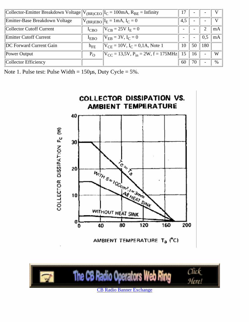
2SC1590Silicon NPN Transistor
RF Power Output
The 2SC1590 is a silicon NPN epitaxial planer typetransistor designed for 136-174MHz RF poweramplifiers on VHF band mobile radio applications.
B E C
Features:
High Power Gain: Gpe >/= 10dB (VCC = 13.5V, PO = 6W, f = 175MHz)●
Ability to Withstand more than 20:1 VSWR Load when Operated at: VCC = 15.2V, PO = 6W, f = 175MHz
●
Application:
4 to 5 Watt Output Power Amplifier Applications in VHF Band●
Absolute Maximum Ratings: (TC = +25°C unless otherwise specified)
Collector-Emitter Voltage (RBE = Infinity), VCEO 17VCollector-Base Voltage, VCBO 35VEmitter-Base Voltage, VEBO 4VCollector Current, IC 12ACollector Power Dissipation (TA = +25°C), PD 1.5WCollector Power Dissipation (TC = +50°C), PD 12.5WOperating Junction Temperature, TJ +150°CStorage Temperature Range, Tstg -55° to +150°CThermal Resistance, Junction-to-Case, RthJC 10°C/WThermal Resistance, Junction-to-Ambient, RthJA 83°C/W

Electrical Characteristics: (TC = +25°C unless otherwise specified)
Parameter Symbol Test Conditions Min Typ Max Unit
Collector-Base Breakdown Voltage V(BR)CBO IC = 10mA, IE = 0 35 - - V
Collector-Emitter Breakdown Voltage V(BR)CEO IC = 50mA, RBE = Infinity 17 - - V
Emitter-Base Breakdown Voltage V(BR)EBO IE = 5mA, IC = 0 4 - - V
Collector Cutoff Current ICBO VCB = 25V IE = 0 - - 500 µA
Emitter Cutoff Current IEBO VEB = 3V, IC = 0 - - 500 µA
DC Forward Current Gain hFE VCE = 10V, IC = 100mA, Note 1 10 50 180
Power Output PO VCC = 13.5V, Pin = 600mW, f = 175MHz 6 7 - W
Collector Efficiency 60 70 - %
Note 1. Pulse test: Pulse Width = 150µs, Duty Cycle = 5%.
CB Radio Banner Exchange

2SC1591Silicon NPN Transistor
RF Power Output
The 2SC1591 is a silicon NPN epitaxial planer typetransistor designed for 136-174MHz RF poweramplifiers on VHF band mobile radio applications.
B E C
Features:
High Power Gain: Gpe >/= 7.5dB (VCC = 13.5V, PO = 14W, f = 175MHz)●
Ability to Withstand more than 20:1 VSWR Load when Operated at: VCC = 15.2V, PO = 18W, f = 175MHz
●
Application:
10 to 14 Watt Output Power Amplifier in VHF Band Mobile Radio Applications●
Absolute Maximum Ratings: (TC = +25°C unless otherwise specified)
Collector-Emitter Voltage (RBE = Infinity), VCEO 17VCollector-Base Voltage, VCBO 35VEmitter-Base Voltage, VEBO 4VCollector Current, IC 3.5ACollector Power Dissipation (TA = +25°C), PD 1.5WCollector Power Dissipation (TC = +50°C), PD 25WOperating Junction Temperature, TJ +175°CStorage Temperature Range, Tstg -55° to +175°CThermal Resistance, Junction-to-Case, RthJC 6°C/WThermal Resistance, Junction-to-Ambient, RthJA 100°C/W

Electrical Characteristics: (TC = +25°C unless otherwise specified)
Parameter Symbol Test Conditions Min Typ Max Unit
Collector-Base Breakdown Voltage V(BR)CBO IC = 10mA, IE = 0 35 - - V
Collector-Emitter Breakdown Voltage V(BR)CEO IC = 50mA, RBE = Infinity 17 - - V
Emitter-Base Breakdown Voltage V(BR)EBO IE = 10mA, IC = 0 4 - - V
Collector Cutoff Current ICBO VCB = 25V IE = 0 - - 1000 µA
Emitter Cutoff Current IEBO VEB = 3V, IC = 0 - - 500 µA
DC Forward Current Gain hFE VCE = 10V, IC = 100mA, Note 1 10 50 180
Power Output PO VCC = 13.5V, Pin = 2.5W, f = 175MHz 14 15 - W
Collector Efficiency 60 70 - %
Note 1. Pulse test: Pulse Width = 150µs, Duty Cycle = 5%.
CB Radio Banner Exchange
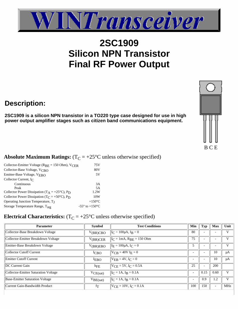
2SC1909Silicon NPN TransistorFinal RF Power Output
Description:
2SC1909 is a silicon NPN transistor in a TO220 type case designed for use in highpower output amplifier stages such as citizen band communications equipment.
B C E
Absolute Maximum Ratings: (TC = +25°C unless otherwise specified)Collector-Emitter Voltage (RBE = 150 Ohm), VCER 75VCollector-Base Voltage, VCBO 80VEmitter-Base Voltage, VEBO 5VCollector Current, IC Continuous Peak
3A5A
Collector Power Dissipation (TA = +25°C), PD 1.2WCollector Power Dissipation (TC = +50°C), PD 10WOperating Junction Temperature, TJ +150°CStorage Temperature Range, Tstg -55° to +150°C
Electrical Characteristics: (TC = +25°C unless otherwise specified)
Parameter Symbol Test Conditions Min Typ Max Unit
Collector-Base Breakdown Voltage V(BR)CBO IC = 100µA, IB = 0 80 - - V
Collector-Emitter Breakdown Voltage V(BR)CER IC = 1mA, RBE = 150 Ohm 75 - - V
Emitter-Base Breakdown Voltage V(BR)EBO IE = 100µA, IC = 0 5 - - V
Collector Cutoff Current ICBO VCB = 40V IE = 0 - - 10 µA
Emitter Cutoff Current IEBO VEB = 4V, IC = 0 - - 10 µA
DC Current Gain hFE VCE = 5V, IC = 0.5A 25 - 200
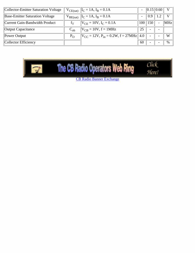
Collector-Emitter Saturation Voltage VCE(sat) IC = 1A, IB = 0.1A - 0.15 0.60 V
Base-Emitter Saturation Voltage VBE(sat) IC = 1A, IB = 0.1A - 0.9 1.2 V
Current Gain-Bandwidth Product fT VCE = 10V, IC = 0.1A 100 150 - MHz

Output Capacitance Cob VCB = 10V, f = 1MHz 25 - -
Power Output PO VCC = 12V, Pin = 0.2W, f = 27MHz 4.0 - - W
Collector Efficiency 60 - - %
CB Radio Banner Exchange

2SC1945Silicon NPN TransistorFinal RF Power Output
The 2SC1945 is a silicon NPN epitaxial planer typetransistor designed for RF power amplifiers on HFband mobile radio applications.
B E C
Features:
High Power Gain: Gpe >/= 14,5dB (VCC = 12V, PO = 18W, f = 27MHz)●
Ability to Withstand Infinite VSWR Load when Operated at: VCC = 16V, PO = 18W, f = 27MHz
●
Application:
10 to 14 Watt Output Power Class AB Amplifier Applications in HF Band●
Absolute Maximum Ratings: (TC = +25°C unless otherwise specified)
Collector-Emitter Voltage (RBE = Infinity), VCEO 40VCollector-Base Voltage, VCBO 80VEmitter-Base Voltage, VEBO 5VCollector Current, IC 6ACollector Power Dissipation (TA = +25°C), PD 1.5WCollector Power Dissipation (TC = +50°C), PD 20WOperating Junction Temperature, TJ +150°CStorage Temperature Range, Tstg -55° to +150°CThermal Resistance, Junction-to-Case, RthJC 6.25°C/WThermal Resistance, Junction-to-Ambient, RthJA 83,3°C/W
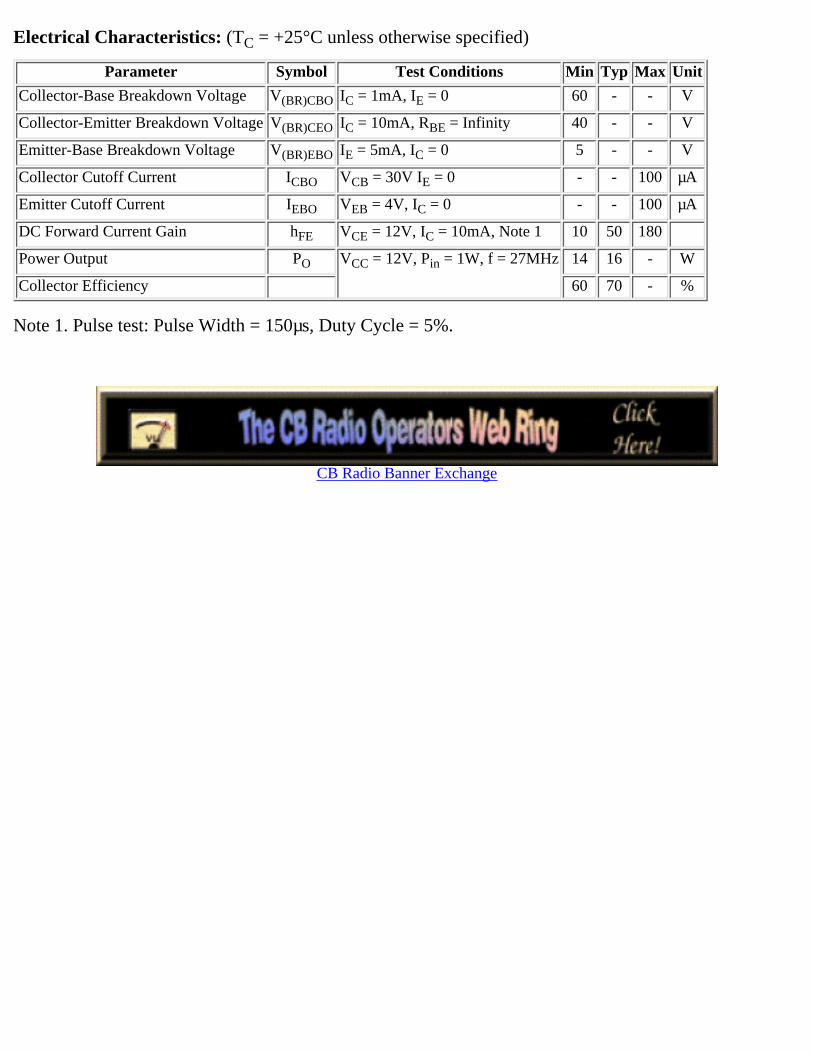
Electrical Characteristics: (TC = +25°C unless otherwise specified)
Parameter Symbol Test Conditions Min Typ Max Unit
Collector-Base Breakdown Voltage V(BR)CBO IC = 1mA, IE = 0 60 - - V
Collector-Emitter Breakdown Voltage V(BR)CEO IC = 10mA, RBE = Infinity 40 - - V
Emitter-Base Breakdown Voltage V(BR)EBO IE = 5mA, IC = 0 5 - - V
Collector Cutoff Current ICBO VCB = 30V IE = 0 - - 100 µA
Emitter Cutoff Current IEBO VEB = 4V, IC = 0 - - 100 µA
DC Forward Current Gain hFE VCE = 12V, IC = 10mA, Note 1 10 50 180
Power Output PO VCC = 12V, Pin = 1W, f = 27MHz 14 16 - W
Collector Efficiency 60 70 - %
Note 1. Pulse test: Pulse Width = 150µs, Duty Cycle = 5%.
CB Radio Banner Exchange
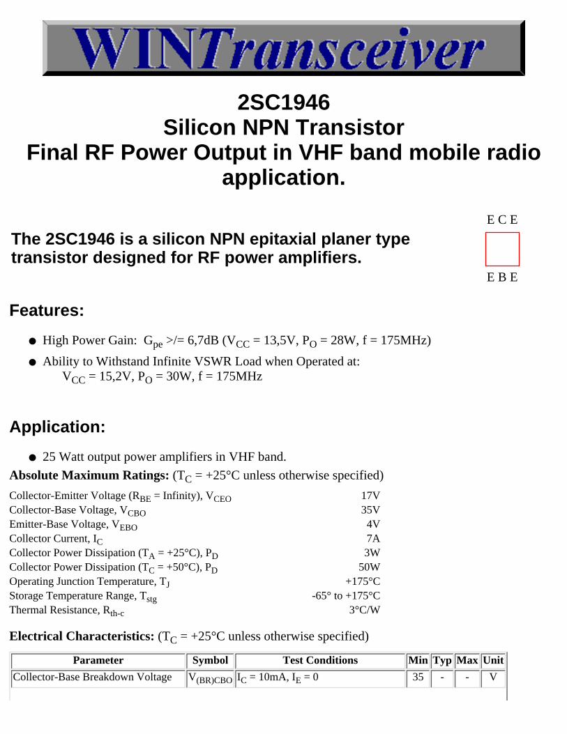
2SC1946Silicon NPN Transistor
Final RF Power Output in VHF band mobile radioapplication.
E C E
The 2SC1946 is a silicon NPN epitaxial planer typetransistor designed for RF power amplifiers.
E B E
Features:
High Power Gain: Gpe >/= 6,7dB (VCC = 13,5V, PO = 28W, f = 175MHz)●
Ability to Withstand Infinite VSWR Load when Operated at: VCC = 15,2V, PO = 30W, f = 175MHz
●
Application:
25 Watt output power amplifiers in VHF band.●
Absolute Maximum Ratings: (TC = +25°C unless otherwise specified)
Collector-Emitter Voltage (RBE = Infinity), VCEO 17VCollector-Base Voltage, VCBO 35VEmitter-Base Voltage, VEBO 4VCollector Current, IC 7ACollector Power Dissipation (TA = +25°C), PD 3WCollector Power Dissipation (TC = +50°C), PD 50WOperating Junction Temperature, TJ +175°CStorage Temperature Range, Tstg -65° to +175°CThermal Resistance, Rth-c 3°C/W
Electrical Characteristics: (TC = +25°C unless otherwise specified)
Parameter Symbol Test Conditions Min Typ Max Unit
Collector-Base Breakdown Voltage V(BR)CBO IC = 10mA, IE = 0 35 - - V
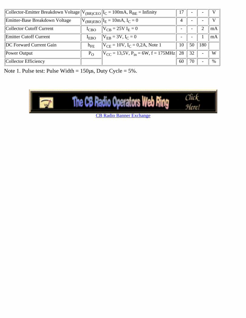
Collector-Emitter Breakdown Voltage V(BR)CEO IC = 100mA, RBE = Infinity 17 - - V
Emitter-Base Breakdown Voltage V(BR)EBO IE = 10mA, IC = 0 4 - - V
Collector Cutoff Current ICBO VCB = 25V IE = 0 - - 2 mA
Emitter Cutoff Current IEBO VEB = 3V, IC = 0 - - 1 mA
DC Forward Current Gain hFE VCE = 10V, IC = 0,2A, Note 1 10 50 180
Power Output PO VCC = 13,5V, Pin = 6W, f = 175MHz 28 32 - W
Collector Efficiency 60 70 - %
Note 1. Pulse test: Pulse Width = 150µs, Duty Cycle = 5%.
CB Radio Banner Exchange
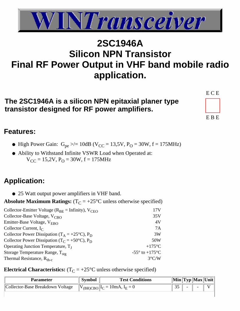
2SC1946ASilicon NPN Transistor
Final RF Power Output in VHF band mobile radioapplication.
E C E
The 2SC1946A is a silicon NPN epitaxial planer typetransistor designed for RF power amplifiers.
E B E
Features:
High Power Gain: Gpe >/= 10dB (VCC = 13,5V, PO = 30W, f = 175MHz)●
Ability to Withstand Infinite VSWR Load when Operated at: VCC = 15,2V, PO = 30W, f = 175MHz
●
Application:
25 Watt output power amplifiers in VHF band.●
Absolute Maximum Ratings: (TC = +25°C unless otherwise specified)
Collector-Emitter Voltage (RBE = Infinity), VCEO 17VCollector-Base Voltage, VCBO 35VEmitter-Base Voltage, VEBO 4VCollector Current, IC 7ACollector Power Dissipation (TA = +25°C), PD 3WCollector Power Dissipation (TC = +50°C), PD 50WOperating Junction Temperature, TJ +175°CStorage Temperature Range, Tstg -55° to +175°CThermal Resistance, Rth-c 3°C/W
Electrical Characteristics: (TC = +25°C unless otherwise specified)
Parameter Symbol Test Conditions Min Typ Max Unit
Collector-Base Breakdown Voltage V(BR)CBO IC = 10mA, IE = 0 35 - - V

Collector-Emitter Breakdown Voltage V(BR)CEO IC = 100mA, RBE = Infinity 17 - - V
Emitter-Base Breakdown Voltage V(BR)EBO IE = 10mA, IC = 0 4 - - V
Collector Cutoff Current ICBO VCB = 25V IE = 0 - - 2 mA
Emitter Cutoff Current IEBO VEB = 3V, IC = 0 - - 1 mA
DC Forward Current Gain hFE VCE = 10V, IC = 0,2A, Note 1 10 50 180
Power Output PO VCC = 13,5V, Pin = 6W, f = 175MHz 30 35 - W
Collector Efficiency 60 70 - %
Note 1. Pulse test: Pulse Width = 150µs, Duty Cycle = 5%.
CB Radio Banner Exchange
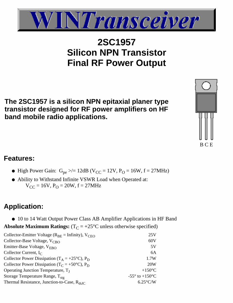
2SC1957Silicon NPN TransistorFinal RF Power Output
The 2SC1957 is a silicon NPN epitaxial planer typetransistor designed for RF power amplifiers on HFband mobile radio applications.
B C E
Features:
High Power Gain: Gpe >/= 12dB (VCC = 12V, PO = 16W, f = 27MHz)●
Ability to Withstand Infinite VSWR Load when Operated at: VCC = 16V, PO = 20W, f = 27MHz
●
Application:
10 to 14 Watt Output Power Class AB Amplifier Applications in HF Band●
Absolute Maximum Ratings: (TC = +25°C unless otherwise specified)
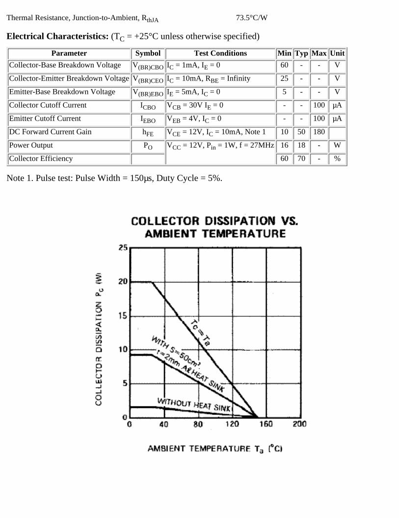
Collector-Emitter Voltage (RBE = Infinity), VCEO 25VCollector-Base Voltage, VCBO 60VEmitter-Base Voltage, VEBO 5VCollector Current, IC 6ACollector Power Dissipation (TA = +25°C), PD 1.7WCollector Power Dissipation (TC = +50°C), PD 20WOperating Junction Temperature, TJ +150°CStorage Temperature Range, Tstg -55° to +150°CThermal Resistance, Junction-to-Case, RthJC 6.25°C/W
Thermal Resistance, Junction-to-Ambient, RthJA 73.5°C/W
Electrical Characteristics: (TC = +25°C unless otherwise specified)
Parameter Symbol Test Conditions Min Typ Max Unit
Collector-Base Breakdown Voltage V(BR)CBO IC = 1mA, IE = 0 60 - - V
Collector-Emitter Breakdown Voltage V(BR)CEO IC = 10mA, RBE = Infinity 25 - - V
Emitter-Base Breakdown Voltage V(BR)EBO IE = 5mA, IC = 0 5 - - V
Collector Cutoff Current ICBO VCB = 30V IE = 0 - - 100 µA
Emitter Cutoff Current IEBO VEB = 4V, IC = 0 - - 100 µA
DC Forward Current Gain hFE VCE = 12V, IC = 10mA, Note 1 10 50 180
Power Output PO VCC = 12V, Pin = 1W, f = 27MHz 16 18 - W
Collector Efficiency 60 70 - %
Note 1. Pulse test: Pulse Width = 150µs, Duty Cycle = 5%.
CB Radio Banner Exchange

2SC1969Silicon NPN TransistorFinal RF Power Output
The 2SC1969 is a silicon NPN epitaxial planer typetransistor designed for RF power amplifiers on HFband mobile radio applications.
B C E
Features:
High Power Gain: Gpe >/= 12dB (VCC = 12V, PO = 16W, f = 27MHz)●
Ability to Withstand Infinite VSWR Load when Operated at: VCC = 16V, PO = 20W, f = 27MHz
●
Application:
10 to 14 Watt Output Power Class AB Amplifier Applications in HF Band●
Absolute Maximum Ratings: (TC = +25°C unless otherwise specified)
Collector-Emitter Voltage (RBE = Infinity), VCEO 25VCollector-Base Voltage, VCBO 60VEmitter-Base Voltage, VEBO 5VCollector Current, IC 6ACollector Power Dissipation (TA = +25°C), PD 1.7WCollector Power Dissipation (TC = +50°C), PD 20WOperating Junction Temperature, TJ +150°CStorage Temperature Range, Tstg -55° to +150°CThermal Resistance, Junction-to-Case, RthJC 6.25°C/W
Thermal Resistance, Junction-to-Ambient, RthJA 73.5°C/W
Electrical Characteristics: (TC = +25°C unless otherwise specified)
Parameter Symbol Test Conditions Min Typ Max Unit
Collector-Base Breakdown Voltage V(BR)CBO IC = 1mA, IE = 0 60 - - V
Collector-Emitter Breakdown Voltage V(BR)CEO IC = 10mA, RBE = Infinity 25 - - V
Emitter-Base Breakdown Voltage V(BR)EBO IE = 5mA, IC = 0 5 - - V
Collector Cutoff Current ICBO VCB = 30V IE = 0 - - 100 µA
Emitter Cutoff Current IEBO VEB = 4V, IC = 0 - - 100 µA
DC Forward Current Gain hFE VCE = 12V, IC = 10mA, Note 1 10 50 180
Power Output PO VCC = 12V, Pin = 1W, f = 27MHz 16 18 - W
Collector Efficiency 60 70 - %
Note 1. Pulse test: Pulse Width = 150µs, Duty Cycle = 5%.

CB Radio Banner Exchange
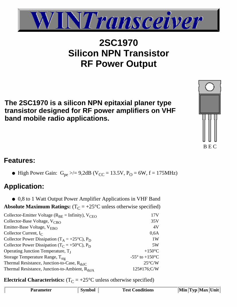
2SC1970Silicon NPN Transistor
RF Power Output
The 2SC1970 is a silicon NPN epitaxial planer typetransistor designed for RF power amplifiers on VHFband mobile radio applications.
B E C
Features:
High Power Gain: Gpe >/= 9,2dB (VCC = 13.5V, PO = 6W, f = 175MHz)●
Application:
0,8 to 1 Watt Output Power Amplifier Applications in VHF Band●
Absolute Maximum Ratings: (TC = +25°C unless otherwise specified)
Collector-Emitter Voltage (RBE = Infinity), VCEO 17VCollector-Base Voltage, VCBO 35VEmitter-Base Voltage, VEBO 4VCollector Current, IC 0,6ACollector Power Dissipation (TA = +25°C), PD 1WCollector Power Dissipation (TC = +50°C), PD 5WOperating Junction Temperature, TJ +150°CStorage Temperature Range, Tstg -55° to +150°CThermal Resistance, Junction-to-Case, RthJC 25°C/WThermal Resistance, Junction-to-Ambient, RthJA 125#176;C/W
Electrical Characteristics: (TC = +25°C unless otherwise specified)
Parameter Symbol Test Conditions Min Typ Max Unit
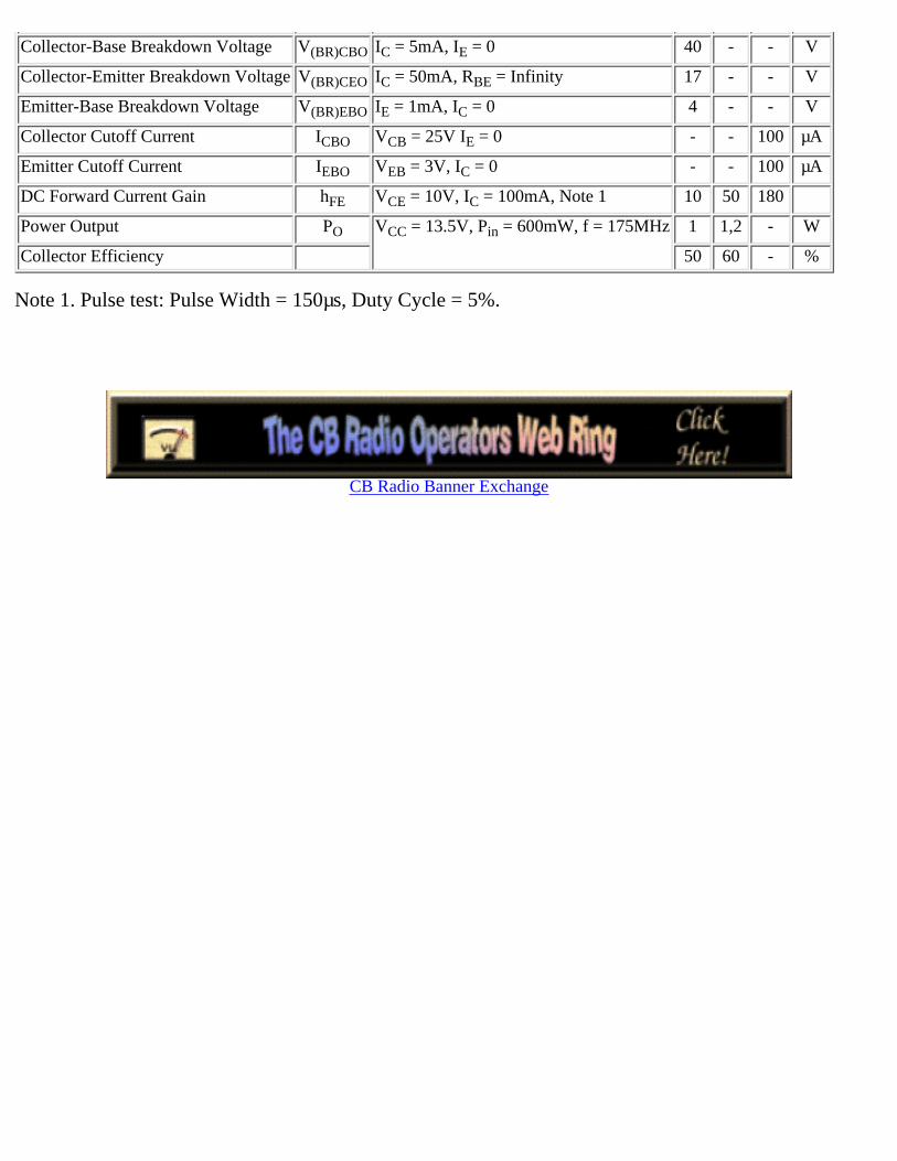
Collector-Base Breakdown Voltage V(BR)CBO IC = 5mA, IE = 0 40 - - V
Collector-Emitter Breakdown Voltage V(BR)CEO IC = 50mA, RBE = Infinity 17 - - V
Emitter-Base Breakdown Voltage V(BR)EBO IE = 1mA, IC = 0 4 - - V
Collector Cutoff Current ICBO VCB = 25V IE = 0 - - 100 µA
Emitter Cutoff Current IEBO VEB = 3V, IC = 0 - - 100 µA
DC Forward Current Gain hFE VCE = 10V, IC = 100mA, Note 1 10 50 180
Power Output PO VCC = 13.5V, Pin = 600mW, f = 175MHz 1 1,2 - W
Collector Efficiency 50 60 - %
Note 1. Pulse test: Pulse Width = 150µs, Duty Cycle = 5%.
CB Radio Banner Exchange

2SC1971Silicon NPN Transistor
RF Power Output
The 2SC1971 is a silicon NPN epitaxial planer typetransistor designed for RF power amplifiers on VHFband mobile radio applications.
B E C
Features:
High Power Gain: Gpe >/= 10dB (VCC = 13.5V, PO = 6W, f = 175MHz)●
Ability to Withstand more than 20:1 VSWR Load when Operated at: VCC = 15.2V, PO = 6W, f = 175MHz
●
Application:
4 to 5 Watt Output Power Amplifier Applications in VHF Band●
Absolute Maximum Ratings: (TC = +25°C unless otherwise specified)
Collector-Emitter Voltage (RBE = Infinity), VCEO 17VCollector-Base Voltage, VCBO 35VEmitter-Base Voltage, VEBO 4VCollector Current, IC 2ACollector Power Dissipation (TA = +25°C), PD 1.5WCollector Power Dissipation (TC = +50°C), PD 12.5WOperating Junction Temperature, TJ +150°CStorage Temperature Range, Tstg -55° to +150°CThermal Resistance, Junction-to-Case, RthJC 10°C/WThermal Resistance, Junction-to-Ambient, RthJA 83°C/W

Electrical Characteristics: (TC = +25°C unless otherwise specified)
Parameter Symbol Test Conditions Min Typ Max Unit
Collector-Base Breakdown Voltage V(BR)CBO IC = 10mA, IE = 0 35 - - V
Collector-Emitter Breakdown Voltage V(BR)CEO IC = 50mA, RBE = Infinity 17 - - V
Emitter-Base Breakdown Voltage V(BR)EBO IE = 5mA, IC = 0 4 - - V
Collector Cutoff Current ICBO VCB = 25V IE = 0 - - 500 µA
Emitter Cutoff Current IEBO VEB = 3V, IC = 0 - - 500 µA
DC Forward Current Gain hFE VCE = 10V, IC = 100mA, Note 1 10 50 180
Power Output PO VCC = 13.5V, Pin = 600mW, f = 175MHz 6 7 - W
Collector Efficiency 60 70 - %
Note 1. Pulse test: Pulse Width = 150µs, Duty Cycle = 5%.
CB Radio Banner Exchange
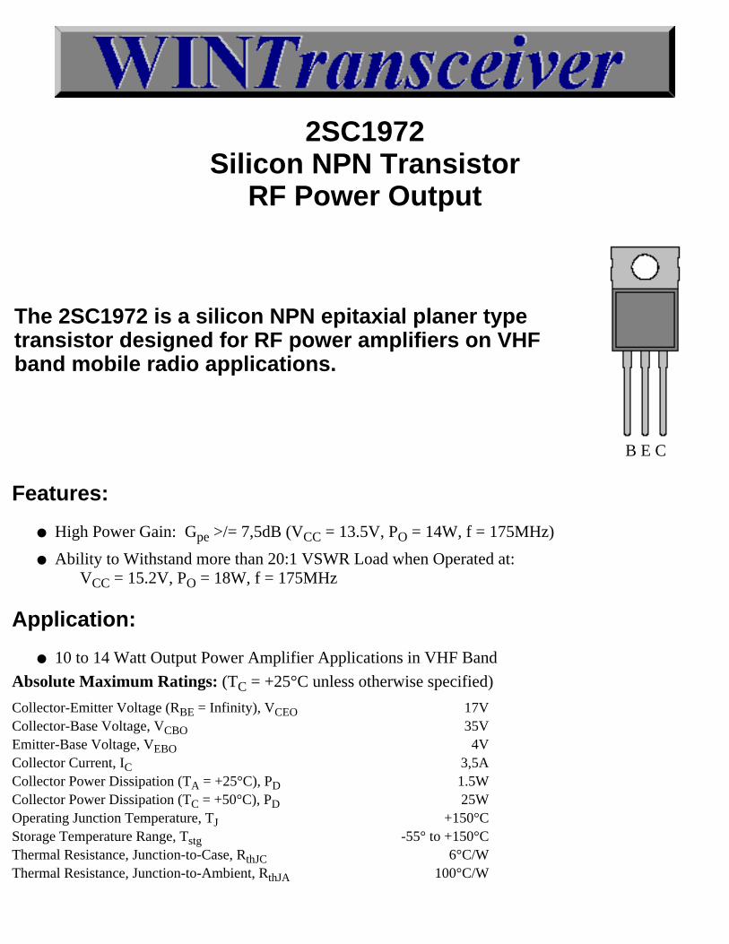
2SC1972Silicon NPN Transistor
RF Power Output
The 2SC1972 is a silicon NPN epitaxial planer typetransistor designed for RF power amplifiers on VHFband mobile radio applications.
B E C
Features:
High Power Gain: Gpe >/= 7,5dB (VCC = 13.5V, PO = 14W, f = 175MHz)●
Ability to Withstand more than 20:1 VSWR Load when Operated at: VCC = 15.2V, PO = 18W, f = 175MHz
●
Application:
10 to 14 Watt Output Power Amplifier Applications in VHF Band●
Absolute Maximum Ratings: (TC = +25°C unless otherwise specified)
Collector-Emitter Voltage (RBE = Infinity), VCEO 17VCollector-Base Voltage, VCBO 35VEmitter-Base Voltage, VEBO 4VCollector Current, IC 3,5ACollector Power Dissipation (TA = +25°C), PD 1.5WCollector Power Dissipation (TC = +50°C), PD 25WOperating Junction Temperature, TJ +150°CStorage Temperature Range, Tstg -55° to +150°CThermal Resistance, Junction-to-Case, RthJC 6°C/WThermal Resistance, Junction-to-Ambient, RthJA 100°C/W

Electrical Characteristics: (TC = +25°C unless otherwise specified)
Parameter Symbol Test Conditions Min Typ Max Unit
Collector-Base Breakdown Voltage V(BR)CBO IC = 10mA, IE = 0 35 - - V
Collector-Emitter Breakdown Voltage V(BR)CEO IC = 50mA, RBE = Infinity 17 - - V
Emitter-Base Breakdown Voltage V(BR)EBO IE = 5mA, IC = 0 4 - - V
Collector Cutoff Current ICBO VCB = 25V IE = 0 - - 1000 µA
Emitter Cutoff Current IEBO VEB = 3V, IC = 0 - - 500 µA
DC Forward Current Gain hFE VCE = 10V, IC = 100mA, Note 1 10 50 180
Power Output PO VCC = 13.5V, Pin = 600mW, f = 175MHz 14 15 - W
Collector Efficiency 60 70 - %
Note 1. Pulse test: Pulse Width = 150µs, Duty Cycle = 5%.
CB Radio Banner Exchange
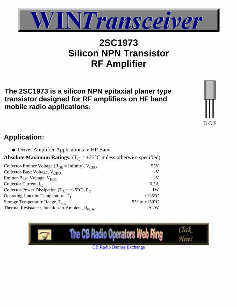
2SC1973Silicon NPN Transistor
RF Amplifier
The 2SC1973 is a silicon NPN epitaxial planer typetransistor designed for RF amplifiers on HF bandmobile radio applications.
B C E
Application:
Driver Amplifier Applications in HF Band●
Absolute Maximum Ratings: (TC = +25°C unless otherwise specified)
Collector-Emitter Voltage (RBE = Infinity), VCEO 55VCollector-Base Voltage, VCBO -VEmitter-Base Voltage, VEBO -VCollector Current, IC 0,5ACollector Power Dissipation (TA = +25°C), PD 1WOperating Junction Temperature, TJ +135°CStorage Temperature Range, Tstg -55° to +150°CThermal Resistance, Junction-to-Ambient, RthJA -°C/W
CB Radio Banner Exchange
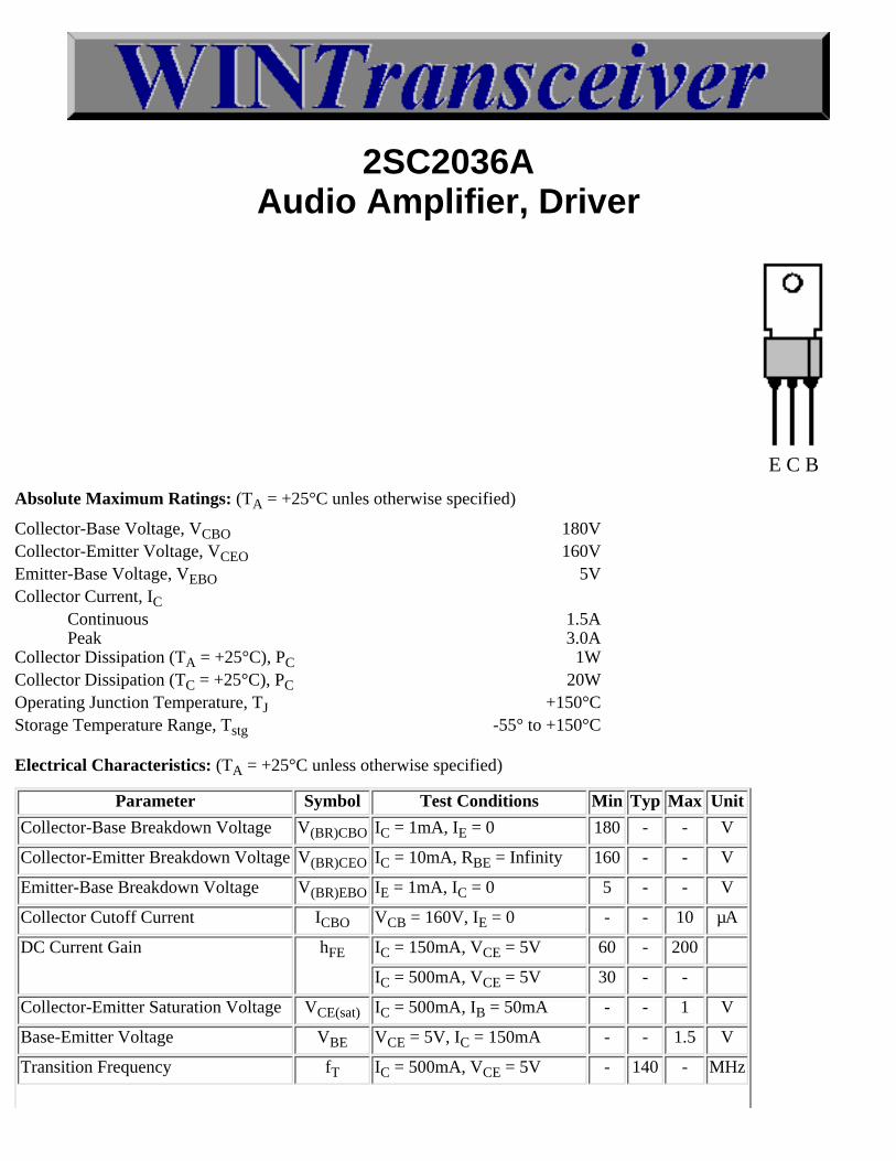
2SC2036AAudio Amplifier, Driver
E C B
Absolute Maximum Ratings: (TA = +25°C unles otherwise specified)
Collector-Base Voltage, VCBO 180VCollector-Emitter Voltage, VCEO 160VEmitter-Base Voltage, VEBO 5VCollector Current, IC Continuous Peak
1.5A3.0A
Collector Dissipation (TA = +25°C), PC 1WCollector Dissipation (TC = +25°C), PC 20WOperating Junction Temperature, TJ +150°CStorage Temperature Range, Tstg -55° to +150°C
Electrical Characteristics: (TA = +25°C unless otherwise specified)
Parameter Symbol Test Conditions Min Typ Max Unit
Collector-Base Breakdown Voltage V(BR)CBO IC = 1mA, IE = 0 180 - - V
Collector-Emitter Breakdown Voltage V(BR)CEO IC = 10mA, RBE = Infinity 160 - - V
Emitter-Base Breakdown Voltage V(BR)EBO IE = 1mA, IC = 0 5 - - V
Collector Cutoff Current ICBO VCB = 160V, IE = 0 - - 10 µA
DC Current Gain hFE IC = 150mA, VCE = 5V 60 - 200
IC = 500mA, VCE = 5V 30 - -
Collector-Emitter Saturation Voltage VCE(sat) IC = 500mA, IB = 50mA - - 1 V
Base-Emitter Voltage VBE VCE = 5V, IC = 150mA - - 1.5 V
Transition Frequency fT IC = 500mA, VCE = 5V - 140 - MHz

Collector Output Capacitance Cob VCB = 10V, IE = 0, f = 1MHz - 14 - pF
CB Radio Banner Exchange

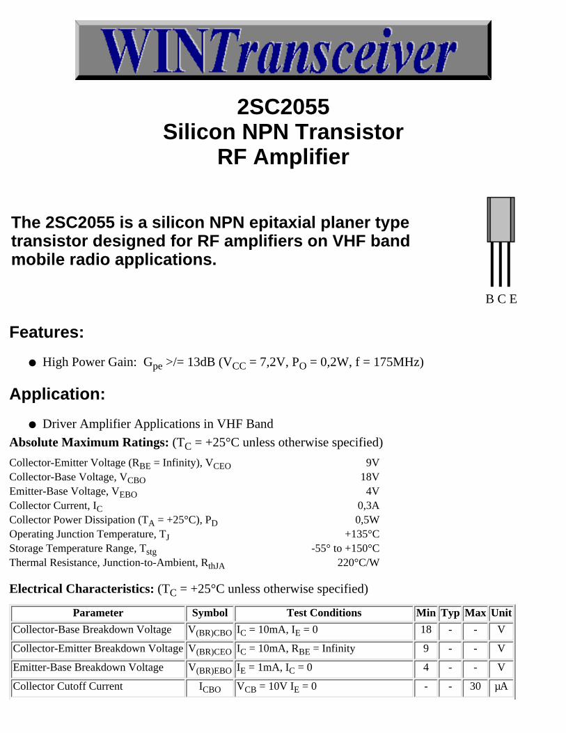
2SC2053Silicon NPN Transistor
RF Amplifier
The 2SC2053 is a silicon NPN epitaxial planer typetransistor designed for RF amplifiers on VHF bandmobile radio applications.
B C E
Features:
High Power Gain: Gpe >/= 15,7dB (VCC = 13,5V, PO = 0,15W, f = 175MHz)●
Application:
Driver Amplifier Applications in VHF Band●
Absolute Maximum Ratings: (TC = +25°C unless otherwise specified)
Collector-Emitter Voltage (RBE = Infinity), VCEO 17VCollector-Base Voltage, VCBO 40VEmitter-Base Voltage, VEBO 4VCollector Current, IC 0,3ACollector Power Dissipation (TA = +25°C), PD 0,6WOperating Junction Temperature, TJ +135°CStorage Temperature Range, Tstg -55° to +150°CThermal Resistance, Junction-to-Ambient, RthJA 183°C/W
Electrical Characteristics: (TC = +25°C unless otherwise specified)
Parameter Symbol Test Conditions Min Typ Max Unit
Collector-Base Breakdown Voltage V(BR)CBO IC = 1mA, IE = 0 40 - - V
Collector-Emitter Breakdown Voltage V(BR)CEO IC = 10mA, RBE = Infinity 17 - - V
Emitter-Base Breakdown Voltage V(BR)EBO IE = 1mA, IC = 0 4 - - V
Collector Cutoff Current ICBO VCB = 15V IE = 0 - - 20 µA

Emitter Cutoff Current IEBO VEB = 3V, IC = 0 - - 20 µA
DC Forward Current Gain hFE VCE = 10V, IC = 100mA, Note 1 10 50 180
Power Output PO VCC = 13.5V, Pin = 4mW, f = 175MHz 0,15 0,2 - W
Collector Efficiency 40 50 - %
Note 1. Pulse test: Pulse Width = 150µs, Duty Cycle = 5%.
CB Radio Banner Exchange
2SC2055Silicon NPN Transistor
RF Amplifier
The 2SC2055 is a silicon NPN epitaxial planer typetransistor designed for RF amplifiers on VHF bandmobile radio applications.
B C E
Features:
High Power Gain: Gpe >/= 13dB (VCC = 7,2V, PO = 0,2W, f = 175MHz)●
Application:
Driver Amplifier Applications in VHF Band●
Absolute Maximum Ratings: (TC = +25°C unless otherwise specified)
Collector-Emitter Voltage (RBE = Infinity), VCEO 9VCollector-Base Voltage, VCBO 18VEmitter-Base Voltage, VEBO 4VCollector Current, IC 0,3ACollector Power Dissipation (TA = +25°C), PD 0,5WOperating Junction Temperature, TJ +135°CStorage Temperature Range, Tstg -55° to +150°CThermal Resistance, Junction-to-Ambient, RthJA 220°C/W
Electrical Characteristics: (TC = +25°C unless otherwise specified)
Parameter Symbol Test Conditions Min Typ Max Unit
Collector-Base Breakdown Voltage V(BR)CBO IC = 10mA, IE = 0 18 - - V
Collector-Emitter Breakdown Voltage V(BR)CEO IC = 10mA, RBE = Infinity 9 - - V
Emitter-Base Breakdown Voltage V(BR)EBO IE = 1mA, IC = 0 4 - - V
Collector Cutoff Current ICBO VCB = 10V IE = 0 - - 30 µA

Emitter Cutoff Current IEBO VEB = 3V, IC = 0 - - 30 µA
DC Forward Current Gain hFE VCE = 7V, IC = 50mA, Note 1 10 50 180
Power Output PO VCC = 13.5V, Pin = 4mW, f = 175MHz 0,2 0,25 - W
Collector Efficiency 50 60 - %
Note 1. Pulse test: Pulse Width = 150µs, Duty Cycle = 5%.
CB Radio Banner Exchange
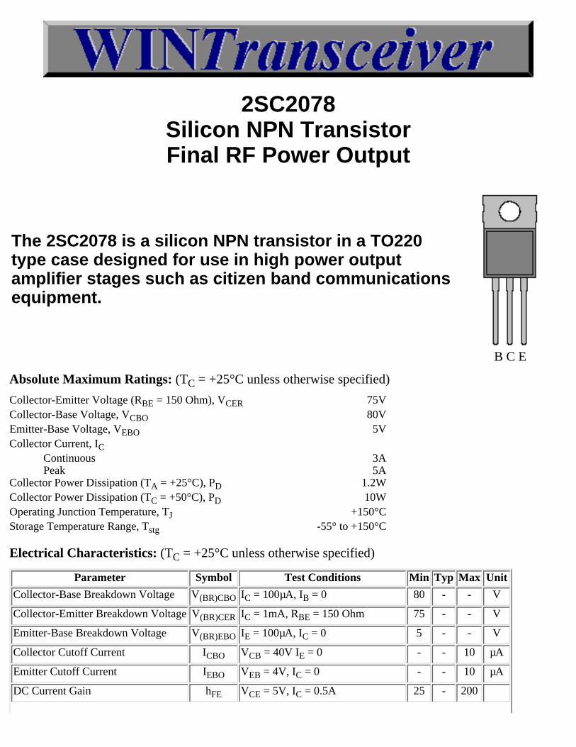
2SC2078Silicon NPN TransistorFinal RF Power Output
The 2SC2078 is a silicon NPN transistor in a TO220type case designed for use in high power outputamplifier stages such as citizen band communicationsequipment.
B C E
Absolute Maximum Ratings: (TC = +25°C unless otherwise specified)
Collector-Emitter Voltage (RBE = 150 Ohm), VCER 75VCollector-Base Voltage, VCBO 80VEmitter-Base Voltage, VEBO 5VCollector Current, IC Continuous Peak
3A5A
Collector Power Dissipation (TA = +25°C), PD 1.2WCollector Power Dissipation (TC = +50°C), PD 10WOperating Junction Temperature, TJ +150°CStorage Temperature Range, Tstg -55° to +150°C
Electrical Characteristics: (TC = +25°C unless otherwise specified)
Parameter Symbol Test Conditions Min Typ Max Unit
Collector-Base Breakdown Voltage V(BR)CBO IC = 100µA, IB = 0 80 - - V
Collector-Emitter Breakdown Voltage V(BR)CER IC = 1mA, RBE = 150 Ohm 75 - - V
Emitter-Base Breakdown Voltage V(BR)EBO IE = 100µA, IC = 0 5 - - V
Collector Cutoff Current ICBO VCB = 40V IE = 0 - - 10 µA
Emitter Cutoff Current IEBO VEB = 4V, IC = 0 - - 10 µA
DC Current Gain hFE VCE = 5V, IC = 0.5A 25 - 200
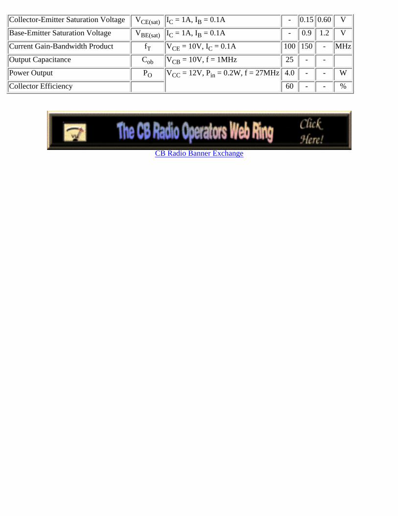
Collector-Emitter Saturation Voltage VCE(sat) IC = 1A, IB = 0.1A - 0.15 0.60 V
Base-Emitter Saturation Voltage VBE(sat) IC = 1A, IB = 0.1A - 0.9 1.2 V
Current Gain-Bandwidth Product fT VCE = 10V, IC = 0.1A 100 150 - MHz
Output Capacitance Cob VCB = 10V, f = 1MHz 25 - -
Power Output PO VCC = 12V, Pin = 0.2W, f = 27MHz 4.0 - - W
Collector Efficiency 60 - - %
CB Radio Banner Exchange

2SC2086Silicon NPN Transistor
RF Amplifier
The 2SC2086 is a silicon NPN epitaxial planer typetransistor designed for RF amplifiers on HF bandmobile radio applications.
B C E
Features:
High Power Gain: Gpe >/= 13dB (VCC = 12V, PO = 0,3W, f = 27MHz)●
Application:
Driver Amplifier Applications in HF Band●
Absolute Maximum Ratings: (TC = +25°C unless otherwise specified)
Collector-Emitter Voltage (RBE = Infinity), VCEO 35VCollector-Base Voltage, VCBO 75VEmitter-Base Voltage, VEBO 4VCollector Current, IC 1ACollector Power Dissipation (TA = +25°C), PD 0,8WOperating Junction Temperature, TJ +135°CStorage Temperature Range, Tstg -55° to +150°CThermal Resistance, Junction-to-Ambient, RthJA 137,5°C/W
Electrical Characteristics: (TC = +25°C unless otherwise specified)
Parameter Symbol Test Conditions Min Typ Max Unit
Collector-Base Breakdown Voltage V(BR)CBO IC = 1mA, IE = 0 75 - - V
Collector-Emitter Breakdown Voltage V(BR)CEO IC = 10mA, RBE = Infinity 35 - - V
Emitter-Base Breakdown Voltage V(BR)EBO IE = 1mA, IC = 0 4 - - V
Collector Cutoff Current ICBO VCB = 30V IE = 0 - - 10 µA
Emitter Cutoff Current IEBO VEB = 3V, IC = 0 - - 100 µA
DC Forward Current Gain hFE VCE = 10V, IC = 100mA, Note 1 35 70 300
Power Output PO VCC = 12V, Pin = 15mW, f = 27MHz 0,3 0,45 - W
Collector Efficiency 50 60 - %
Note 1. Pulse test: Pulse Width = 150µs, Duty Cycle = 5%.
CB Radio Banner Exchange
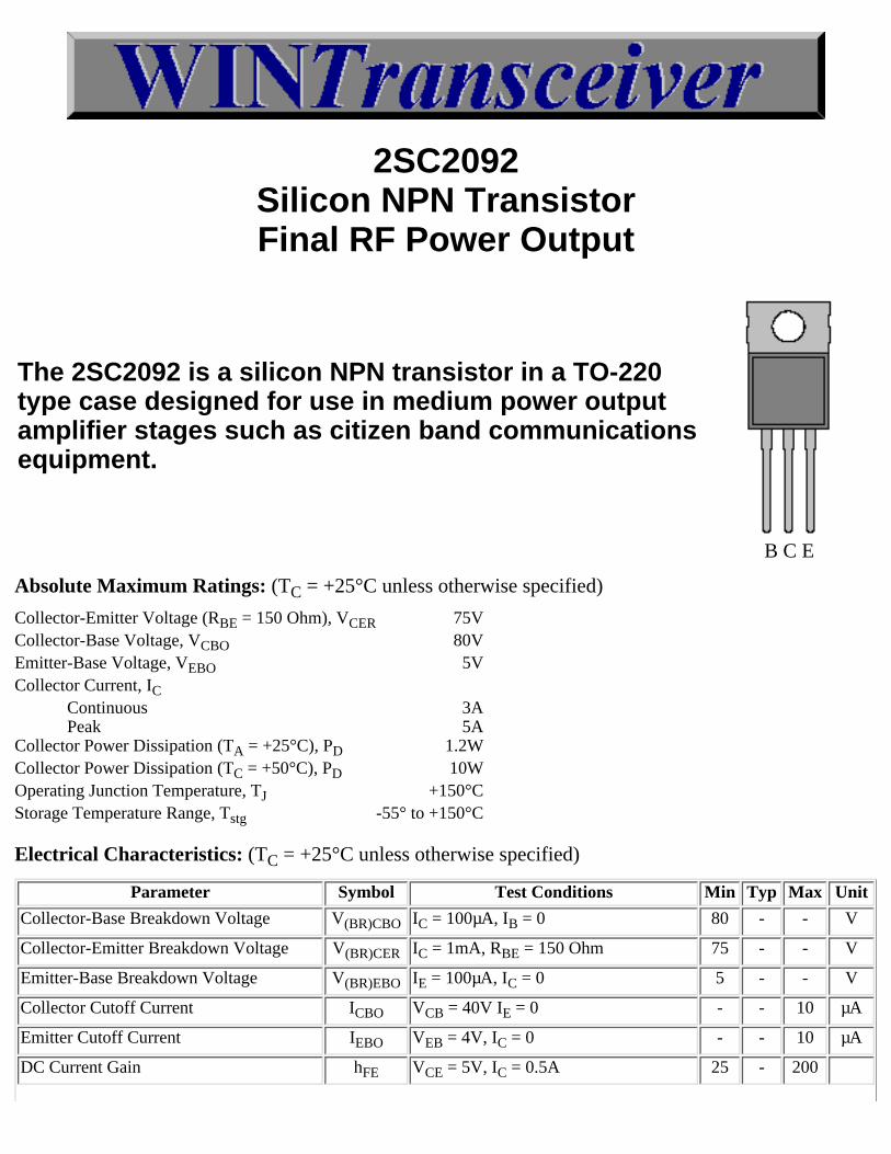
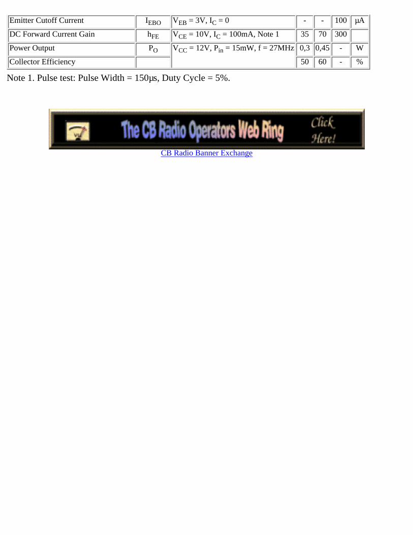
2SC2092Silicon NPN TransistorFinal RF Power Output
The 2SC2092 is a silicon NPN transistor in a TO-220type case designed for use in medium power outputamplifier stages such as citizen band communicationsequipment.
B C E
Absolute Maximum Ratings: (TC = +25°C unless otherwise specified)
Collector-Emitter Voltage (RBE = 150 Ohm), VCER 75VCollector-Base Voltage, VCBO 80VEmitter-Base Voltage, VEBO 5VCollector Current, IC Continuous Peak
3A5A
Collector Power Dissipation (TA = +25°C), PD 1.2WCollector Power Dissipation (TC = +50°C), PD 10WOperating Junction Temperature, TJ +150°CStorage Temperature Range, Tstg -55° to +150°C
Electrical Characteristics: (TC = +25°C unless otherwise specified)
Parameter Symbol Test Conditions Min Typ Max Unit
Collector-Base Breakdown Voltage V(BR)CBO IC = 100µA, IB = 0 80 - - V
Collector-Emitter Breakdown Voltage V(BR)CER IC = 1mA, RBE = 150 Ohm 75 - - V
Emitter-Base Breakdown Voltage V(BR)EBO IE = 100µA, IC = 0 5 - - V
Collector Cutoff Current ICBO VCB = 40V IE = 0 - - 10 µA
Emitter Cutoff Current IEBO VEB = 4V, IC = 0 - - 10 µA
DC Current Gain hFE VCE = 5V, IC = 0.5A 25 - 200
Collector-Emitter Saturation Voltage VCE(sat) IC = 1A, IB = 0.1A - 0.15 0.60 V
Base-Emitter Saturation Voltage VBE(sat) IC = 1A, IB = 0.1A - 0.9 1.2 V
Current Gain-Bandwidth Product fT VCE = 10V, IC = 0.1A 100 150 - MHz
Output Capacitance Cob VCB = 10V, f = 1MHz 25 - -
Power Output PO VCC = 12V, Pin = 0.2W, f = 27MHz 4.0 - - W
Collector Efficiency 60 - - %
CB Radio Banner Exchange
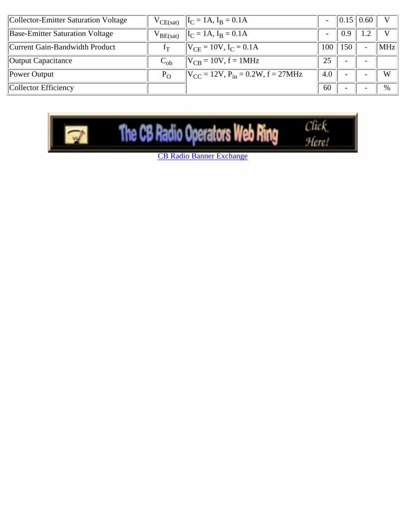
2SC2094Silicon NPN Transistor
Final RF Power Output in VHF band mobile radioapplication.
E C E
The 2SC2094 is a silicon NPN epitaxial planer typetransistor designed for RF power amplifiers.
E B E
Features:
High Power Gain: Gpe >/= 8,8dB (VCC = 13,5V, PO = 15W, f = 175MHz)●
Ability to Withstand Infinite VSWR Load when Operated at: VCC = 15,2V, PO = 18W, f = 175MHz
●
Application:
10 to 14 Watt output linear power amplifiers in VHF band.●
Absolute Maximum Ratings: (TC = +25°C unless otherwise specified)
Collector-Emitter Voltage (RBE = Infinity), VCEO 17VCollector-Base Voltage, VCBO 40VEmitter-Base Voltage, VEBO 4,5VCollector Current, IC 3,5ACollector Power Dissipation (TA = +25°C), PD 2WCollector Power Dissipation (TC = +50°C), PD 30WOperating Junction Temperature, TJ +175°CStorage Temperature Range, Tstg -55° to +175°CThermal Resistance, Rth-c 5°C/W
Electrical Characteristics: (TC = +25°C unless otherwise specified)
Parameter Symbol Test Conditions Min Typ Max Unit
Collector-Base Breakdown Voltage V(BR)CBO IC = 10mA, IE = 0 40 - - V
Collector-Emitter Breakdown Voltage V(BR)CEO IC = 100mA, RBE = Infinity 17 - - V
Emitter-Base Breakdown Voltage V(BR)EBO IE = 1mA, IC = 0 4,5 - - V
Collector Cutoff Current ICBO VCB = 25V IE = 0 - - 2 mA
Emitter Cutoff Current IEBO VEB = 3V, IC = 0 - - 0,5 mA
DC Forward Current Gain hFE VCE = 10V, IC = 0,1A, Note 1 10 50 180
Power Output PO VCC = 13,5V, Pin = 2W, f = 175MHz 15 16 - W
Collector Efficiency 60 70 - %
Note 1. Pulse test: Pulse Width = 150µs, Duty Cycle = 5%.
CB Radio Banner Exchange
2SC2166Silicon NPN TransistorFinal RF Power Output
The 2SC2166 is a silicon NPN epitaxial planer typetransistor designed for RF power amplifiers on HFband mobile radio applications.
B C E
Features:
High Power Gain: Gpe >/= 13,8dB (VCC = 12V, PO = 6W, f = 27MHz)●
Application:
3 to 4 Watt Output Power Class AB Amplifier Applications in HF Band●
Absolute Maximum Ratings: (TC = +25°C unless otherwise specified)
Collector-Emitter Voltage (RBE = Infinity), VCEO 75VCollector-Base Voltage, VCBO 75VEmitter-Base Voltage, VEBO 5VCollector Current, IC 4ACollector Power Dissipation (TA = +25°C), PD 1.5WCollector Power Dissipation (TC = +50°C), PD 12,5WOperating Junction Temperature, TJ +150°CStorage Temperature Range, Tstg -55° to +150°CThermal Resistance, Junction-to-Case, RthJC 10°C/WThermal Resistance, Junction-to-Ambient, RthJA 83°C/W
Electrical Characteristics: (TC = +25°C unless otherwise specified)
Parameter Symbol Test Conditions Min Typ Max Unit
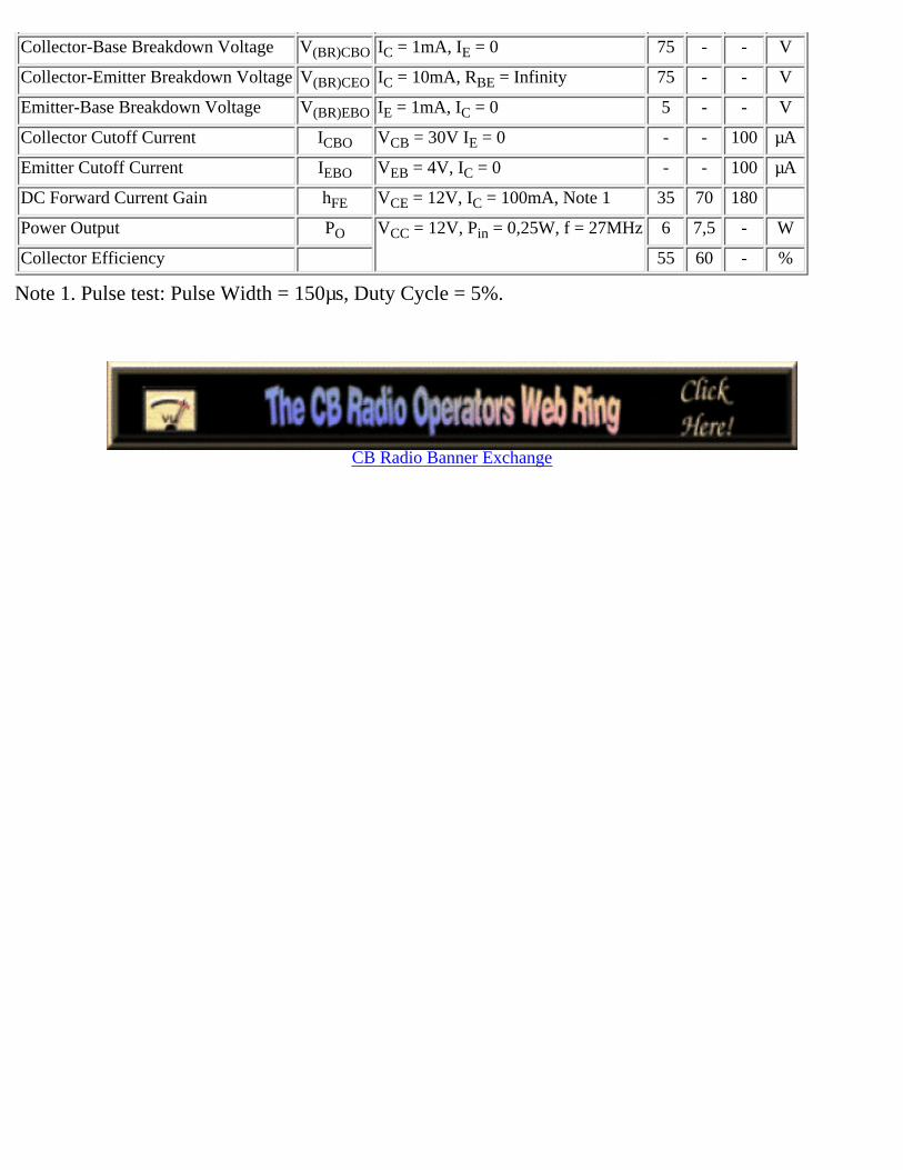
Collector-Base Breakdown Voltage V(BR)CBO IC = 1mA, IE = 0 75 - - V
Collector-Emitter Breakdown Voltage V(BR)CEO IC = 10mA, RBE = Infinity 75 - - V
Emitter-Base Breakdown Voltage V(BR)EBO IE = 1mA, IC = 0 5 - - V
Collector Cutoff Current ICBO VCB = 30V IE = 0 - - 100 µA
Emitter Cutoff Current IEBO VEB = 4V, IC = 0 - - 100 µA
DC Forward Current Gain hFE VCE = 12V, IC = 100mA, Note 1 35 70 180
Power Output PO VCC = 12V, Pin = 0,25W, f = 27MHz 6 7,5 - W
Collector Efficiency 55 60 - %
Note 1. Pulse test: Pulse Width = 150µs, Duty Cycle = 5%.
CB Radio Banner Exchange
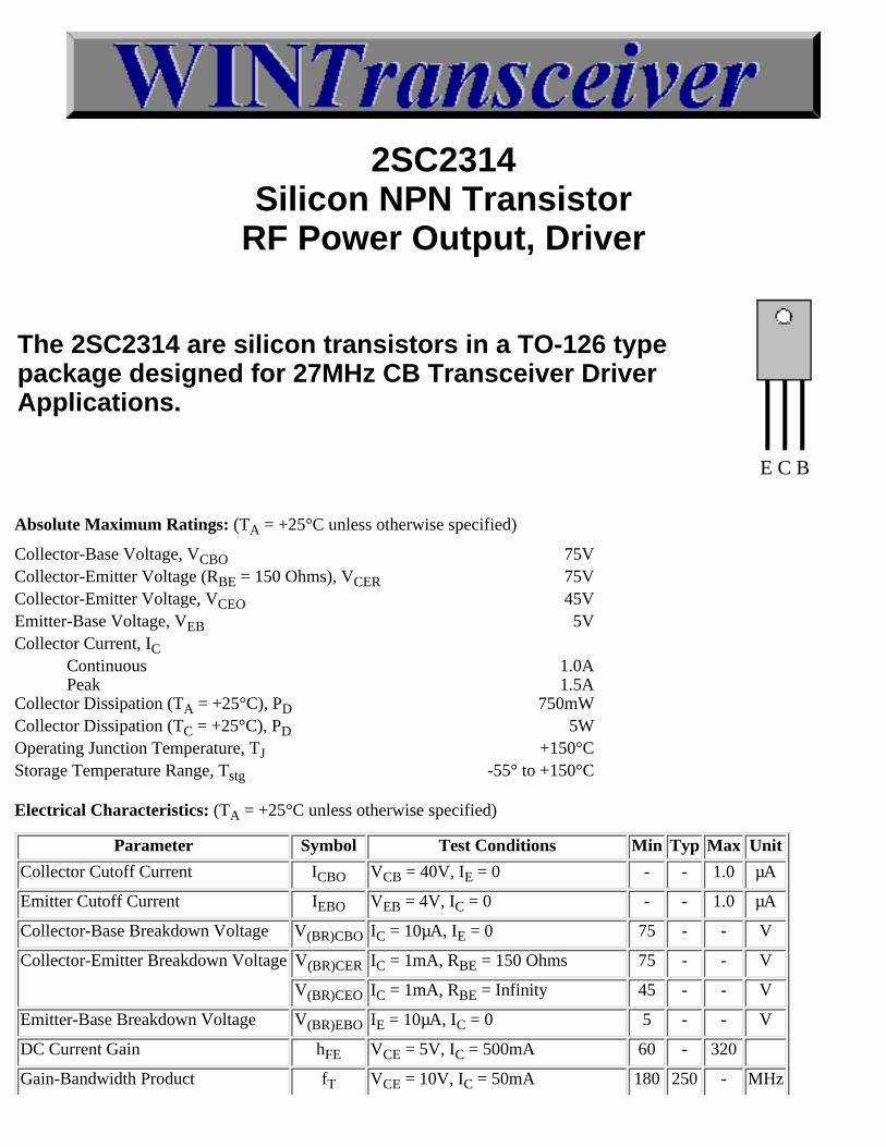
2SC2314Silicon NPN Transistor
RF Power Output, Driver
The 2SC2314 are silicon transistors in a TO-126 typepackage designed for 27MHz CB Transceiver DriverApplications.
E C B
Absolute Maximum Ratings: (TA = +25°C unless otherwise specified)
Collector-Base Voltage, VCBO 75VCollector-Emitter Voltage (RBE = 150 Ohms), VCER 75VCollector-Emitter Voltage, VCEO 45VEmitter-Base Voltage, VEB 5VCollector Current, IC Continuous Peak
1.0A1.5A
Collector Dissipation (TA = +25°C), PD 750mWCollector Dissipation (TC = +25°C), PD 5WOperating Junction Temperature, TJ +150°CStorage Temperature Range, Tstg -55° to +150°C
Electrical Characteristics: (TA = +25°C unless otherwise specified)
Parameter Symbol Test Conditions Min Typ Max Unit
Collector Cutoff Current ICBO VCB = 40V, IE = 0 - - 1.0 µA
Emitter Cutoff Current IEBO VEB = 4V, IC = 0 - - 1.0 µA
Collector-Base Breakdown Voltage V(BR)CBO IC = 10µA, IE = 0 75 - - V
Collector-Emitter Breakdown Voltage V(BR)CER IC = 1mA, RBE = 150 Ohms 75 - - V
V(BR)CEO IC = 1mA, RBE = Infinity 45 - - V
Emitter-Base Breakdown Voltage V(BR)EBO IE = 10µA, IC = 0 5 - - V
DC Current Gain hFE VCE = 5V, IC = 500mA 60 - 320
Gain-Bandwidth Product fT VCE = 10V, IC = 50mA 180 250 - MHz

Collector-Emitter Saturation Voltage VCE(sat) IC = 500mA, IB = 50mA - 0.2 0.6 V
Base-Emitter Saturation Voltage VBE(sat) IC = 500mA, IB = 50mA - 0.9 1.2 V
Output Capacitance Cob VCB = 10V, f = 1MHz - 15 25 pF
Output Power PO VCC = 12V, f = 27MHz, Pi = 35mW 1.0 1.8 - W
Collector Efficiency 60 - - %
Medlem av HyperBanner Norge
CB Radio Banner Exchange
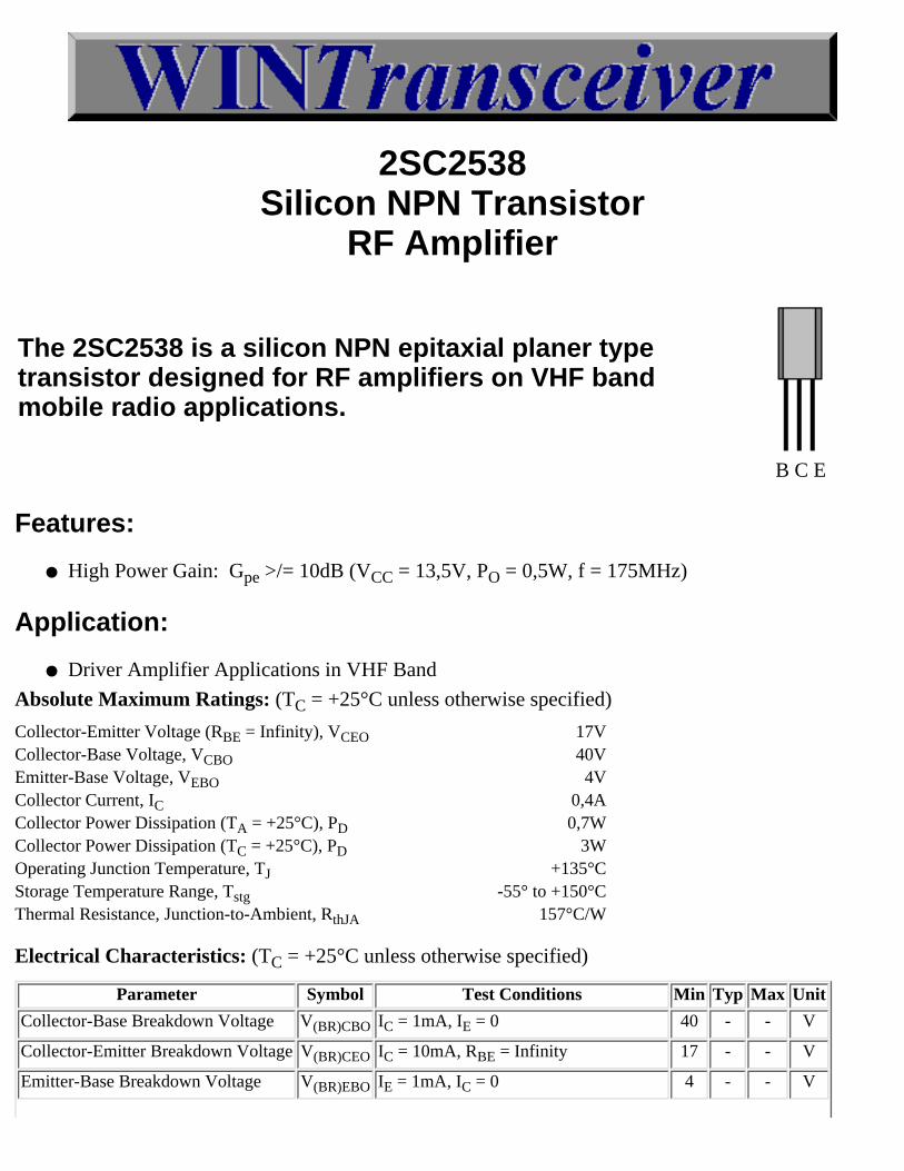
2SC2538Silicon NPN Transistor
RF Amplifier
The 2SC2538 is a silicon NPN epitaxial planer typetransistor designed for RF amplifiers on VHF bandmobile radio applications.
B C E
Features:
High Power Gain: Gpe >/= 10dB (VCC = 13,5V, PO = 0,5W, f = 175MHz)●
Application:
Driver Amplifier Applications in VHF Band●
Absolute Maximum Ratings: (TC = +25°C unless otherwise specified)
Collector-Emitter Voltage (RBE = Infinity), VCEO 17VCollector-Base Voltage, VCBO 40VEmitter-Base Voltage, VEBO 4VCollector Current, IC 0,4ACollector Power Dissipation (TA = +25°C), PD 0,7WCollector Power Dissipation (TC = +25°C), PD 3WOperating Junction Temperature, TJ +135°CStorage Temperature Range, Tstg -55° to +150°CThermal Resistance, Junction-to-Ambient, RthJA 157°C/W
Electrical Characteristics: (TC = +25°C unless otherwise specified)
Parameter Symbol Test Conditions Min Typ Max Unit
Collector-Base Breakdown Voltage V(BR)CBO IC = 1mA, IE = 0 40 - - V
Collector-Emitter Breakdown Voltage V(BR)CEO IC = 10mA, RBE = Infinity 17 - - V
Emitter-Base Breakdown Voltage V(BR)EBO IE = 1mA, IC = 0 4 - - V
Collector Cutoff Current ICBO VCB = 15V IE = 0 - - 100 µA
Emitter Cutoff Current IEBO VEB = 3V, IC = 0 - - 200 µA
DC Forward Current Gain hFE VCE = 10V, IC = 500mA, Note 1 10 80 300
Power Output PO VCC = 13.5V, Pin = 50mW, f = 175MHz 0,5 0,6 - W
Collector Efficiency 45 55 - %
Note 1. Pulse test: Pulse Width = 150µs, Duty Cycle = 5%.
CB Radio Banner Exchange
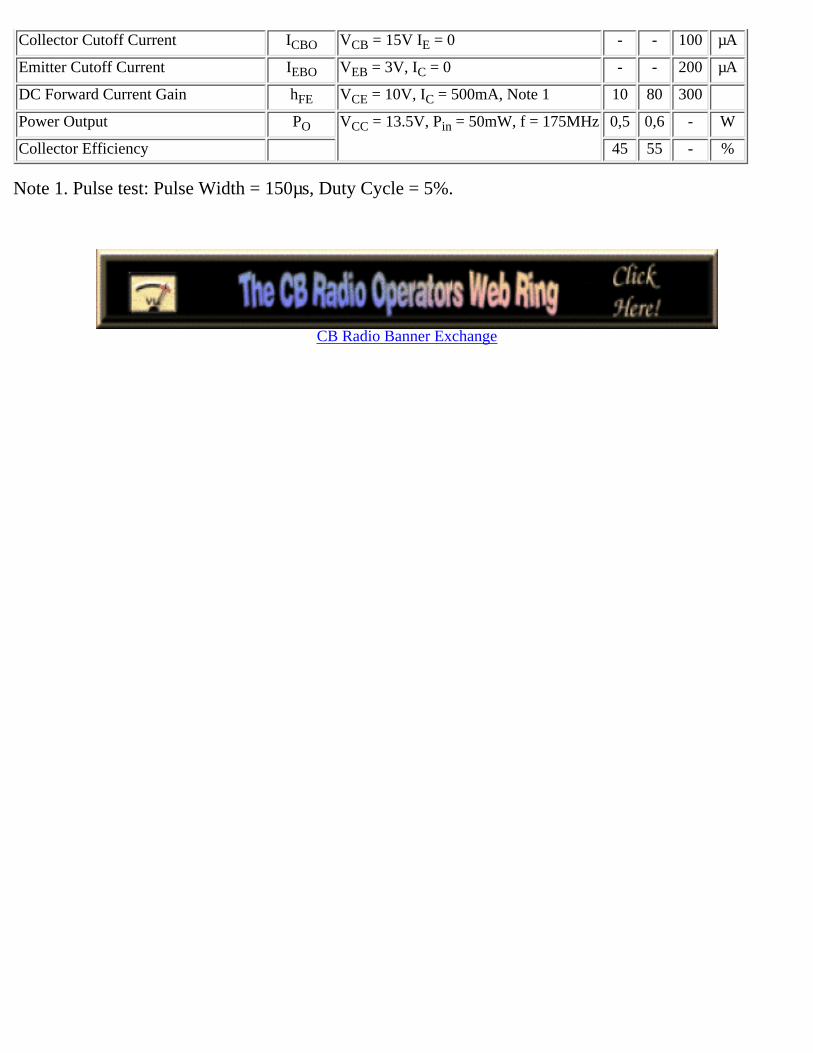
2SC3133Silicon NPN TransistorFinal RF Power Output
The 2SC3133 is a silicon NPN epitaxial planer typetransistor designed for RF power amplifiers on HFband mobile radio applications.
B E C
Features:
High Power Gain: Gpe >/= 14dB (VCC = 12V, PO = 13W, f = 27MHz)●
Ability to Withstand Infinite VSWR Load when Operated at: VCC = 16V, PO = 16W, f = 27MHz
●
Application:
10 Watt Output Power SSB Amplifier Applications in HF Band●
Absolute Maximum Ratings: (TC = +25°C unless otherwise specified)
Collector-Emitter Voltage (RBE = Infinity), VCEO 25VCollector-Base Voltage, VCBO 70VEmitter-Base Voltage, VEBO 5VCollector Current, IC 6ACollector Power Dissipation (TA = +25°C), PD 1.5WCollector Power Dissipation (TC = +50°C), PD 20WOperating Junction Temperature, TJ +150°CStorage Temperature Range, Tstg -55° to +150°CThermal Resistance, Junction-to-Case, RthJC 6.25°C/WThermal Resistance, Junction-to-Ambient, RthJA 83,3°C/W

Electrical Characteristics: (TC = +25°C unless otherwise specified)
Parameter Symbol Test Conditions Min Typ Max Unit
Collector-Base Breakdown Voltage V(BR)CBO IC = 1mA, IE = 0 60 - - V
Collector-Emitter Breakdown Voltage V(BR)CEO IC = 5mA, RBE = Infinity 25 - - V
Emitter-Base Breakdown Voltage V(BR)EBO IE = 1mA, IC = 0 5 - - V
Collector Cutoff Current ICBO VCB = 30V IE = 0 - - 500 µA
Emitter Cutoff Current IEBO VEB = 4V, IC = 0 - - 500 µA
DC Forward Current Gain hFE VCE = 12V, IC = 10mA, Note 1 10 50 180
Power Output PO VCC = 12V, Pin = 0,5W, f = 27MHz 13 16 - W
Collector Efficiency 60 70 - %
Note 1. Pulse test: Pulse Width = 150µs, Duty Cycle = 5%.
CB Radio Banner Exchange
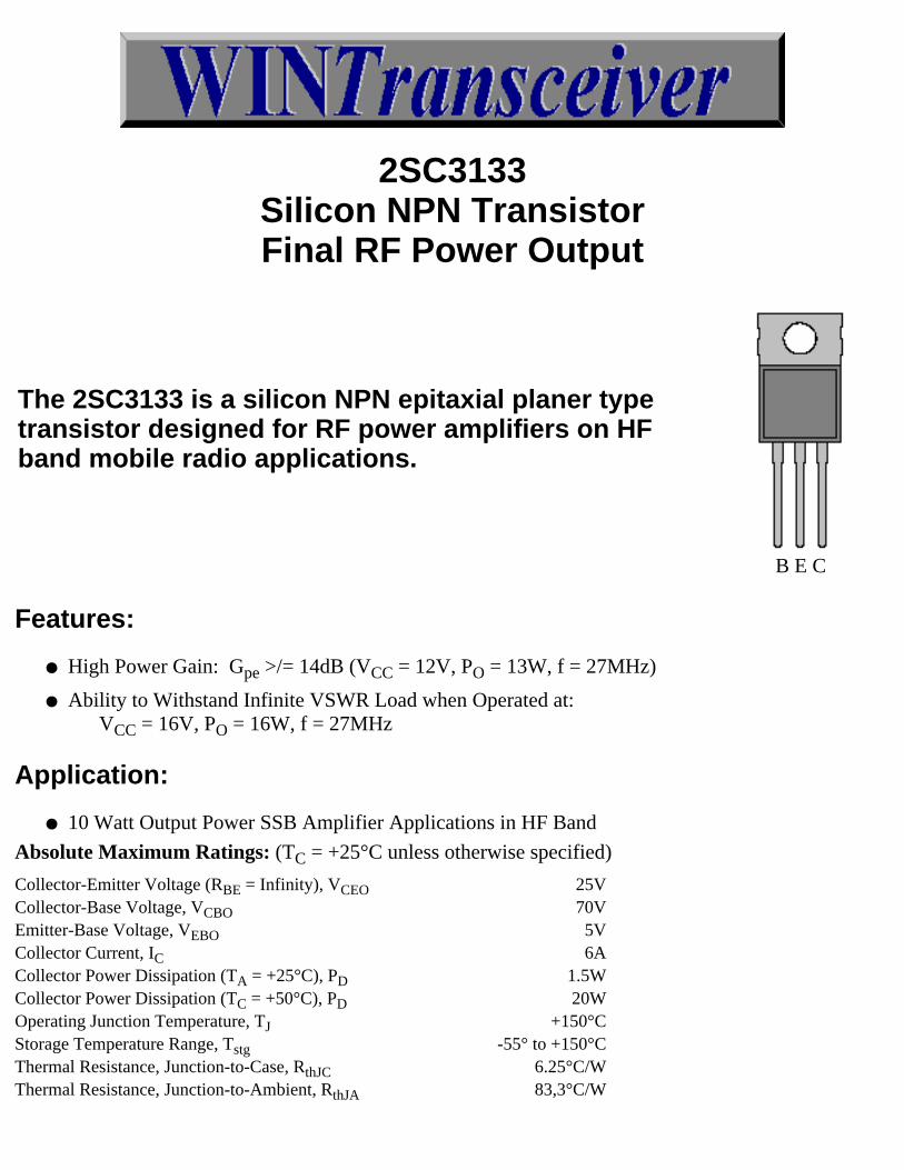
2SC3299Power Amp Driver, Output Switch
The 2SC3299 are silicon transistors in a TO-220 typepackage designed for general purpose poweramplification and switching such as output or driverstages in applications such as switching regulators,converters, and power amplifiers.
B C E
Features:
Low Collector-Emitter saturation Voltage●
Fast Switching Speeds●
Complementary Pairs Simplifies Design●
Absolute Maximum Ratings:Collector-Emitter Voltage, VCEO 80VEmitter-Base Voltage, VEB 5VCollector Current, IC Continuous Peak (Note 1)
10A20A
Total Power Dissipation (TC = +25°C), PD 50WTotal Power Dissipation (TA = +25°C), PD 1.67WOperating Junction Temperature Range, TJ -55° to +150°CStorage Temperature Range, Tstg -55° to +150°CThermal Resistance, Junction-to-Case, RthJC 2.5°C/WThermal Resistance, Junction-to-Ambient, RthJA 75°C/WLead Temperature (During Soldering, 1/8" from case, 5sec), TL +275°C
Note 1. Pulse Width </= 6ms, Duty Cycle </= 50%.
Electrical Characteristics: (TC = +25°C unless otherwise specified)
Parameter Symbol Test Conditions Min Typ Max Unit
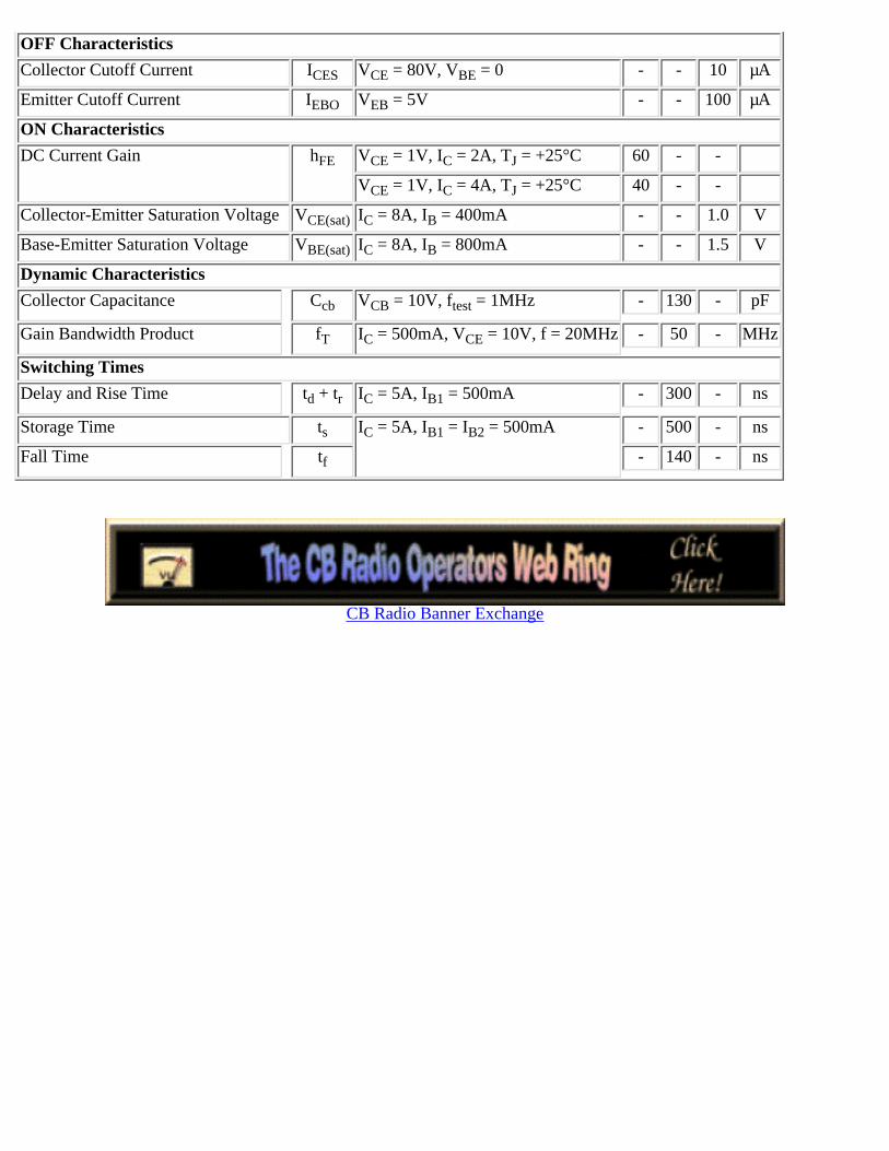
OFF Characteristics
Collector Cutoff Current ICES VCE = 80V, VBE = 0 - - 10 µA
Emitter Cutoff Current IEBO VEB = 5V - - 100 µA
ON Characteristics
DC Current Gain hFE VCE = 1V, IC = 2A, TJ = +25°C 60 - -
VCE = 1V, IC = 4A, TJ = +25°C 40 - -
Collector-Emitter Saturation Voltage VCE(sat) IC = 8A, IB = 400mA - - 1.0 V
Base-Emitter Saturation Voltage VBE(sat) IC = 8A, IB = 800mA - - 1.5 V
Dynamic Characteristics
Collector Capacitance Ccb VCB = 10V, ftest = 1MHz - 130 - pF
Gain Bandwidth Product fT IC = 500mA, VCE = 10V, f = 20MHz - 50 - MHz
Switching Times
Delay and Rise Time td + tr IC = 5A, IB1 = 500mA - 300 - ns
Storage Time ts IC = 5A, IB1 = IB2 = 500mA - 500 - ns
Fall Time tf - 140 - ns
CB Radio Banner Exchange
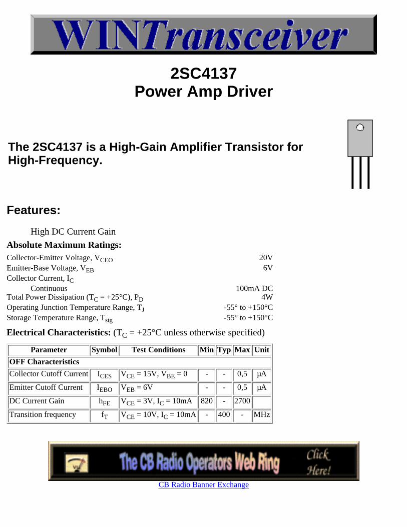
2SC4137Power Amp Driver
The 2SC4137 is a High-Gain Amplifier Transistor forHigh-Frequency.
Features:
High DC Current Gain
Absolute Maximum Ratings:Collector-Emitter Voltage, VCEO 20VEmitter-Base Voltage, VEB 6VCollector Current, IC Continuous 100mA DCTotal Power Dissipation (TC = +25°C), PD 4WOperating Junction Temperature Range, TJ -55° to +150°CStorage Temperature Range, Tstg -55° to +150°C
Electrical Characteristics: (TC = +25°C unless otherwise specified)
Parameter Symbol Test Conditions Min Typ Max Unit
OFF Characteristics
Collector Cutoff Current ICES VCE = 15V, VBE = 0 - - 0,5 µA
Emitter Cutoff Current IEBO VEB = 6V - - 0,5 µA
DC Current Gain hFE VCE = 3V, IC = 10mA 820 - 2700
Transition frequency fT VCE = 10V, IC = 10mA - 400 - MHz
CB Radio Banner Exchange


KTC1006Silicon NPN Transistor
The KTC1006 is a silicon NPN epitaxial planar typetransistor designed for CB tranceiver TX driveramplifier application.
E C B
Features:
High Power Gain●
Wide Area of Safe Operation.●
Application:
Recommended for Driver Stage Application of AM Transmitter.●
Absolute Maximum Ratings: (TC = +25°C unless otherwise specified)
Collector-Emitter Voltage (RBE = Infinity), VCEO 80VCollector-Base Voltage, VCBO 80VEmitter-Base Voltage, VEBO 5VCollector Current, IC 800mACollector Power Dissipation (TC = +50°C), PD 1WOperating Junction Temperature, TJ +150°CStorage Temperature Range, Tstg -55° to +150°C
Electrical Characteristics: (TC = +25°C unless otherwise specified)
Parameter Symbol Test Conditions Min Typ Max Unit
Collector Cutoff Current ICBO VCB = 60V IE = 0 - - 0,1 µA
Collector Cutoff Current ICER VCB = 80V RBE = 220ohm - - 0,1 µA
DC Forward Current Gain hFE VCE = 2V, IC = 150mA 100 - -
Transition Frequency fT VCE = 5V, IC = 500mA - 150 - MHz

CB Radio Banner Exchange
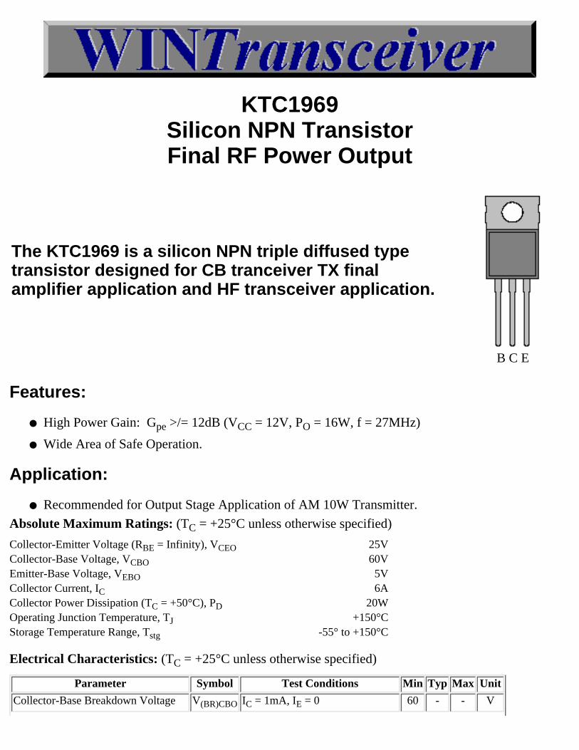
KTC1969Silicon NPN TransistorFinal RF Power Output
The KTC1969 is a silicon NPN triple diffused typetransistor designed for CB tranceiver TX finalamplifier application and HF transceiver application.
B C E
Features:
High Power Gain: Gpe >/= 12dB (VCC = 12V, PO = 16W, f = 27MHz)●
Wide Area of Safe Operation.●
Application:
Recommended for Output Stage Application of AM 10W Transmitter.●
Absolute Maximum Ratings: (TC = +25°C unless otherwise specified)
Collector-Emitter Voltage (RBE = Infinity), VCEO 25VCollector-Base Voltage, VCBO 60VEmitter-Base Voltage, VEBO 5VCollector Current, IC 6ACollector Power Dissipation (TC = +50°C), PD 20WOperating Junction Temperature, TJ +150°CStorage Temperature Range, Tstg -55° to +150°C
Electrical Characteristics: (TC = +25°C unless otherwise specified)
Parameter Symbol Test Conditions Min Typ Max Unit
Collector-Base Breakdown Voltage V(BR)CBO IC = 1mA, IE = 0 60 - - V

Collector-Emitter Breakdown Voltage V(BR)CEO IC = 10mA, RBE = Infinity 25 - - V
Emitter-Base Breakdown Voltage V(BR)EBO IE = 5mA, IC = 0 5 - - V
Collector Cutoff Current ICBO VCB = 30V IE = 0 - - 10 µA
Emitter Cutoff Current IEBO VEB = 4V, IC = 0 - - 100 µA
DC Forward Current Gain hFE VCE = 12V, IC = 10mA, Note 1 55 - 180
Transition Frequency fT VCE = 5V, IC = 500mA 100 - - MHz
Power Output PO VCC = 12V, Pin = 1W, f = 27MHz 16 - - W
CB Radio Banner Exchange
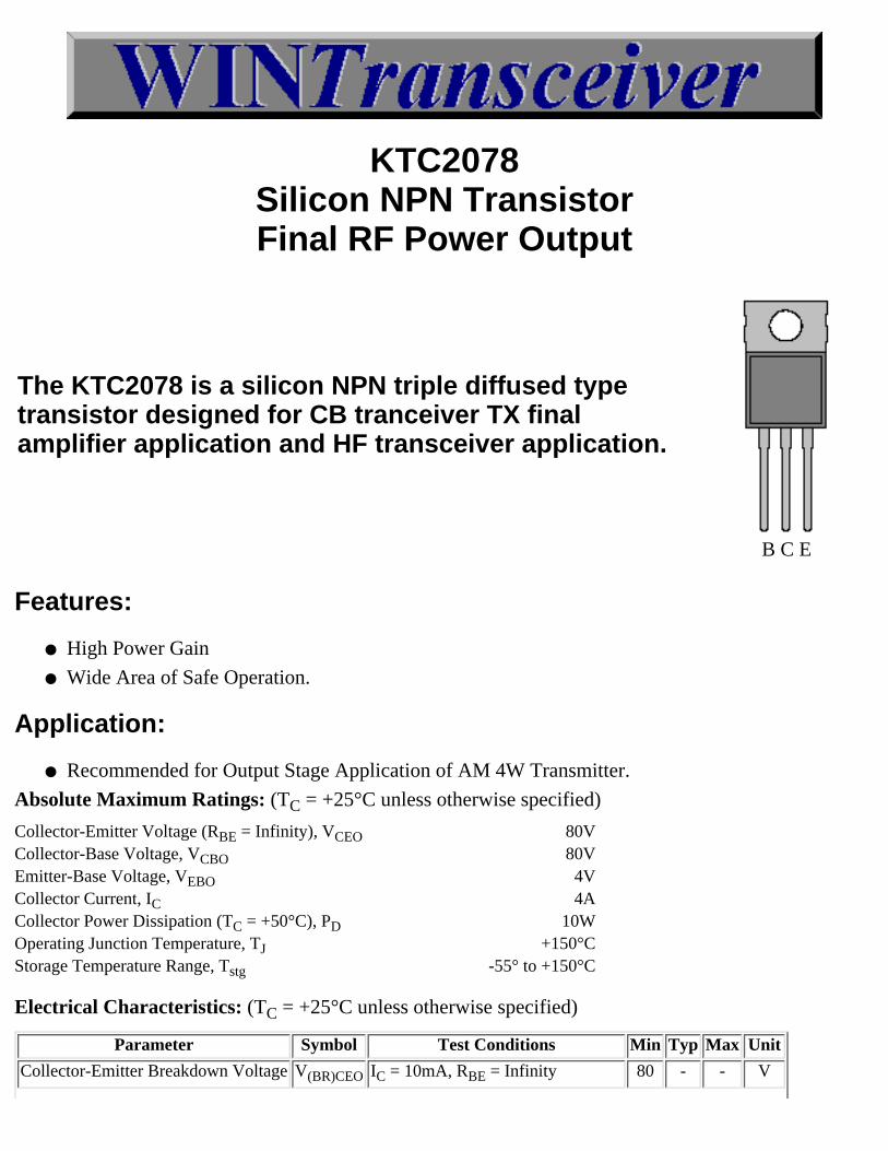
KTC2078Silicon NPN TransistorFinal RF Power Output
The KTC2078 is a silicon NPN triple diffused typetransistor designed for CB tranceiver TX finalamplifier application and HF transceiver application.
B C E
Features:
High Power Gain●
Wide Area of Safe Operation.●
Application:
Recommended for Output Stage Application of AM 4W Transmitter.●
Absolute Maximum Ratings: (TC = +25°C unless otherwise specified)
Collector-Emitter Voltage (RBE = Infinity), VCEO 80VCollector-Base Voltage, VCBO 80VEmitter-Base Voltage, VEBO 4VCollector Current, IC 4ACollector Power Dissipation (TC = +50°C), PD 10WOperating Junction Temperature, TJ +150°CStorage Temperature Range, Tstg -55° to +150°C
Electrical Characteristics: (TC = +25°C unless otherwise specified)
Parameter Symbol Test Conditions Min Typ Max Unit
Collector-Emitter Breakdown Voltage V(BR)CEO IC = 10mA, RBE = Infinity 80 - - V

Emitter-Base Breakdown Voltage V(BR)EBO IE = 1mA, IC = 0 4 - - V
Collector Cutoff Current ICBO VCB = 30V IE = 0 - - 10 µA
DC Forward Current Gain hFE VCE = 5V, IC = 0,5mA 100 - 200
Transition Frequency fT VCE = 5V, IC = 500mA 100 - - MHz
Power Output PO VCC = 12V, Pin = 0,3W, f = 27MHz 4 - - W
CB Radio Banner Exchange
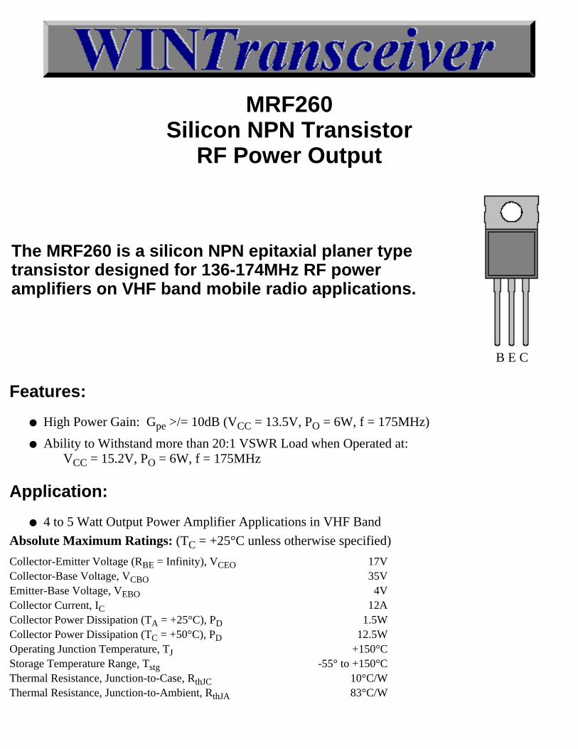
MRF260Silicon NPN Transistor
RF Power Output
The MRF260 is a silicon NPN epitaxial planer typetransistor designed for 136-174MHz RF poweramplifiers on VHF band mobile radio applications.
B E C
Features:
High Power Gain: Gpe >/= 10dB (VCC = 13.5V, PO = 6W, f = 175MHz)●
Ability to Withstand more than 20:1 VSWR Load when Operated at: VCC = 15.2V, PO = 6W, f = 175MHz
●
Application:
4 to 5 Watt Output Power Amplifier Applications in VHF Band●
Absolute Maximum Ratings: (TC = +25°C unless otherwise specified)
Collector-Emitter Voltage (RBE = Infinity), VCEO 17VCollector-Base Voltage, VCBO 35VEmitter-Base Voltage, VEBO 4VCollector Current, IC 12ACollector Power Dissipation (TA = +25°C), PD 1.5WCollector Power Dissipation (TC = +50°C), PD 12.5WOperating Junction Temperature, TJ +150°CStorage Temperature Range, Tstg -55° to +150°CThermal Resistance, Junction-to-Case, RthJC 10°C/WThermal Resistance, Junction-to-Ambient, RthJA 83°C/W
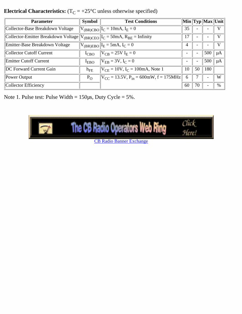
Electrical Characteristics: (TC = +25°C unless otherwise specified)
Parameter Symbol Test Conditions Min Typ Max Unit
Collector-Base Breakdown Voltage V(BR)CBO IC = 10mA, IE = 0 35 - - V
Collector-Emitter Breakdown Voltage V(BR)CEO IC = 50mA, RBE = Infinity 17 - - V
Emitter-Base Breakdown Voltage V(BR)EBO IE = 5mA, IC = 0 4 - - V
Collector Cutoff Current ICBO VCB = 25V IE = 0 - - 500 µA
Emitter Cutoff Current IEBO VEB = 3V, IC = 0 - - 500 µA
DC Forward Current Gain hFE VCE = 10V, IC = 100mA, Note 1 10 50 180
Power Output PO VCC = 13.5V, Pin = 600mW, f = 175MHz 6 7 - W
Collector Efficiency 60 70 - %
Note 1. Pulse test: Pulse Width = 150µs, Duty Cycle = 5%.
CB Radio Banner Exchange

MRF262Silicon NPN Transistor
RF Power Output
The MRF262 is a silicon NPN epitaxial planer typetransistor designed for 136-174MHz RF poweramplifiers on VHF band mobile radio applications.
B E C
Features:
High Power Gain: Gpe >/= 7.5dB (VCC = 13.5V, PO = 14W, f = 175MHz)●
Ability to Withstand more than 20:1 VSWR Load when Operated at: VCC = 15.2V, PO = 18W, f = 175MHz
●
Application:
10 to 14 Watt Output Power Amplifier in VHF Band Mobile Radio Applications●
Absolute Maximum Ratings: (TC = +25°C unless otherwise specified)
Collector-Emitter Voltage (RBE = Infinity), VCEO 17VCollector-Base Voltage, VCBO 35VEmitter-Base Voltage, VEBO 4VCollector Current, IC 3.5ACollector Power Dissipation (TA = +25°C), PD 1.5WCollector Power Dissipation (TC = +50°C), PD 25WOperating Junction Temperature, TJ +175°CStorage Temperature Range, Tstg -55° to +175°CThermal Resistance, Junction-to-Case, RthJC 6°C/WThermal Resistance, Junction-to-Ambient, RthJA 100°C/W

Electrical Characteristics: (TC = +25°C unless otherwise specified)
Parameter Symbol Test Conditions Min Typ Max Unit
Collector-Base Breakdown Voltage V(BR)CBO IC = 10mA, IE = 0 35 - - V
Collector-Emitter Breakdown Voltage V(BR)CEO IC = 50mA, RBE = Infinity 17 - - V
Emitter-Base Breakdown Voltage V(BR)EBO IE = 10mA, IC = 0 4 - - V
Collector Cutoff Current ICBO VCB = 25V IE = 0 - - 1000 µA
Emitter Cutoff Current IEBO VEB = 3V, IC = 0 - - 500 µA
DC Forward Current Gain hFE VCE = 10V, IC = 100mA, Note 1 10 50 180
Power Output PO VCC = 13.5V, Pin = 2.5W, f = 175MHz 14 15 - W
Collector Efficiency 60 70 - %
Note 1. Pulse test: Pulse Width = 150µs, Duty Cycle = 5%.
CB Radio Banner Exchange
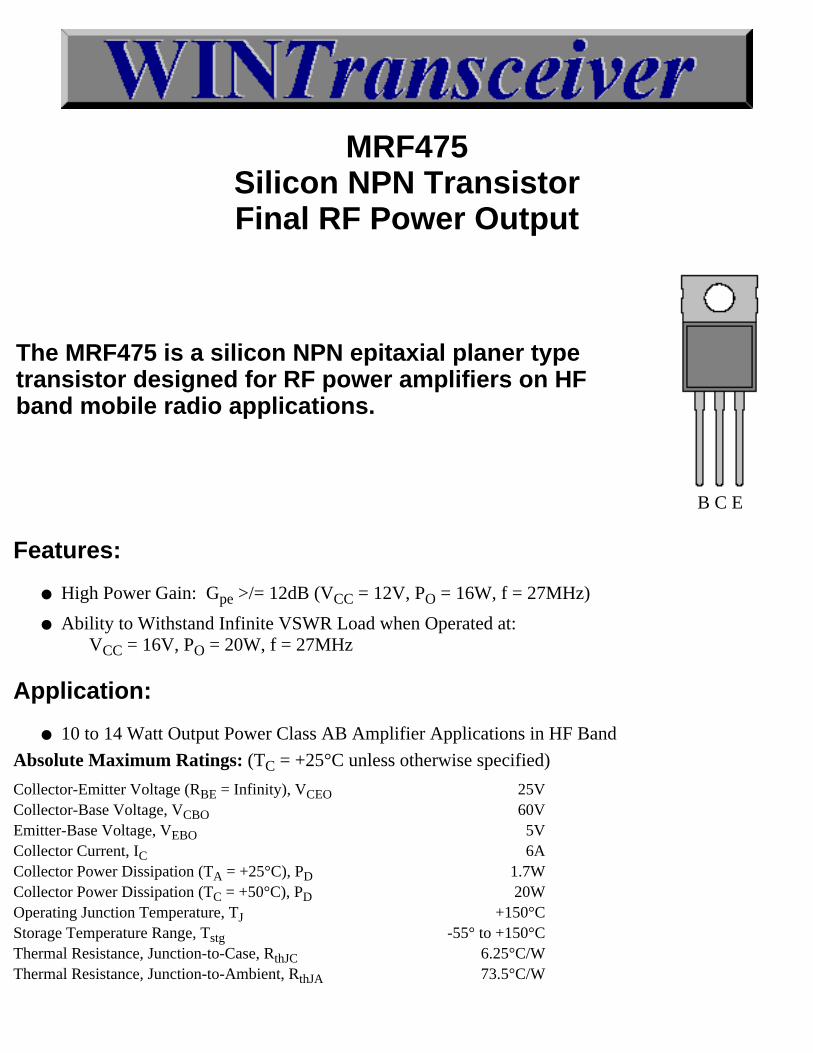
MRF475Silicon NPN TransistorFinal RF Power Output
The MRF475 is a silicon NPN epitaxial planer typetransistor designed for RF power amplifiers on HFband mobile radio applications.
B C E
Features:
High Power Gain: Gpe >/= 12dB (VCC = 12V, PO = 16W, f = 27MHz)●
Ability to Withstand Infinite VSWR Load when Operated at: VCC = 16V, PO = 20W, f = 27MHz
●
Application:
10 to 14 Watt Output Power Class AB Amplifier Applications in HF Band●
Absolute Maximum Ratings: (TC = +25°C unless otherwise specified)
Collector-Emitter Voltage (RBE = Infinity), VCEO 25VCollector-Base Voltage, VCBO 60VEmitter-Base Voltage, VEBO 5VCollector Current, IC 6ACollector Power Dissipation (TA = +25°C), PD 1.7WCollector Power Dissipation (TC = +50°C), PD 20WOperating Junction Temperature, TJ +150°CStorage Temperature Range, Tstg -55° to +150°CThermal Resistance, Junction-to-Case, RthJC 6.25°C/WThermal Resistance, Junction-to-Ambient, RthJA 73.5°C/W

Electrical Characteristics: (TC = +25°C unless otherwise specified)
Parameter Symbol Test Conditions Min Typ Max Unit
Collector-Base Breakdown Voltage V(BR)CBO IC = 1mA, IE = 0 60 - - V
Collector-Emitter Breakdown Voltage V(BR)CEO IC = 10mA, RBE = Infinity 25 - - V
Emitter-Base Breakdown Voltage V(BR)EBO IE = 5mA, IC = 0 5 - - V
Collector Cutoff Current ICBO VCB = 30V IE = 0 - - 100 µA
Emitter Cutoff Current IEBO VEB = 4V, IC = 0 - - 100 µA
DC Forward Current Gain hFE VCE = 12V, IC = 10mA, Note 1 10 50 180
Power Output PO VCC = 12V, Pin = 1W, f = 27MHz 16 18 - W
Collector Efficiency 60 70 - %
Note 1. Pulse test: Pulse Width = 150µs, Duty Cycle = 5%.
CB Radio Banner Exchange
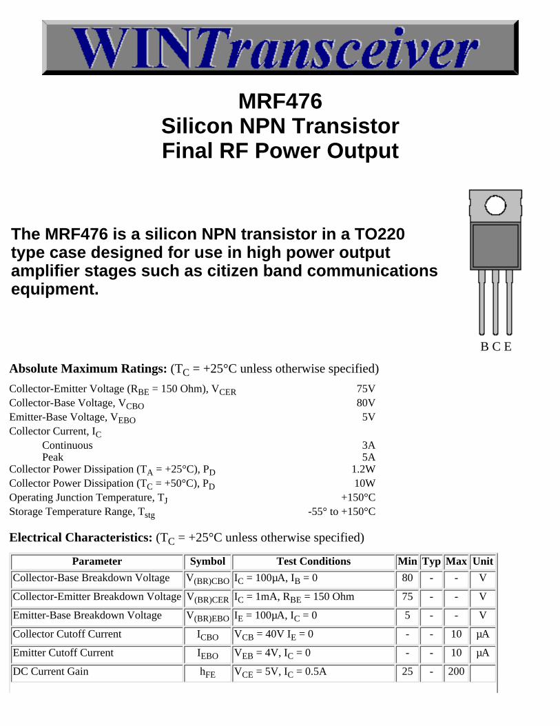
MRF476Silicon NPN TransistorFinal RF Power Output
The MRF476 is a silicon NPN transistor in a TO220type case designed for use in high power outputamplifier stages such as citizen band communicationsequipment.
B C E
Absolute Maximum Ratings: (TC = +25°C unless otherwise specified)
Collector-Emitter Voltage (RBE = 150 Ohm), VCER 75VCollector-Base Voltage, VCBO 80VEmitter-Base Voltage, VEBO 5VCollector Current, IC Continuous Peak
3A5A
Collector Power Dissipation (TA = +25°C), PD 1.2WCollector Power Dissipation (TC = +50°C), PD 10WOperating Junction Temperature, TJ +150°CStorage Temperature Range, Tstg -55° to +150°C
Electrical Characteristics: (TC = +25°C unless otherwise specified)
Parameter Symbol Test Conditions Min Typ Max Unit
Collector-Base Breakdown Voltage V(BR)CBO IC = 100µA, IB = 0 80 - - V
Collector-Emitter Breakdown Voltage V(BR)CER IC = 1mA, RBE = 150 Ohm 75 - - V
Emitter-Base Breakdown Voltage V(BR)EBO IE = 100µA, IC = 0 5 - - V
Collector Cutoff Current ICBO VCB = 40V IE = 0 - - 10 µA
Emitter Cutoff Current IEBO VEB = 4V, IC = 0 - - 10 µA
DC Current Gain hFE VCE = 5V, IC = 0.5A 25 - 200
Collector-Emitter Saturation Voltage VCE(sat) IC = 1A, IB = 0.1A - 0.15 0.60 V
Base-Emitter Saturation Voltage VBE(sat) IC = 1A, IB = 0.1A - 0.9 1.2 V
Current Gain-Bandwidth Product fT VCE = 10V, IC = 0.1A 100 150 - MHz
Output Capacitance Cob VCB = 10V, f = 1MHz 25 - -
Power Output PO VCC = 12V, Pin = 0.2W, f = 27MHz 4.0 - - W
Collector Efficiency 60 - - %
CB Radio Banner Exchange

MRF485Silicon NPN TransistorFinal RF Power Output
The MRF485 is a silicon NPN epitaxial planer typetransistor designed for RF power amplifiers on HFband mobile radio applications.
Features:
High Power Gain: Gpe >/= 12dB (VCC = 12V, PO = 16W, f = 27MHz)●
Ability to Withstand Infinite VSWR Load when Operated at: VCC = 16V, PO = 20W, f = 27MHz
●
Application:
10 to 14 Watt Output Power Class AB Amplifier Applications in HF Band●
Absolute Maximum Ratings: (TC = +25°C unless otherwise specified)
Collector-Emitter Voltage (RBE = Infinity), VCEO 25VCollector-Base Voltage, VCBO 60VEmitter-Base Voltage, VEBO 5VCollector Current, IC 6ACollector Power Dissipation (TA = +25°C), PD 1.7WCollector Power Dissipation (TC = +50°C), PD 20WOperating Junction Temperature, TJ +150°CStorage Temperature Range, Tstg -55° to +150°CThermal Resistance, Junction-to-Case, RthJC 6.25°C/WThermal Resistance, Junction-to-Ambient, RthJA 73.5°C/W
Electrical Characteristics: (TC = +25°C unless otherwise specified)
Parameter Symbol Test Conditions Min Typ Max Unit
Collector-Base Breakdown Voltage V(BR)CBO IC = 1mA, IE = 0 60 - - V
Collector-Emitter Breakdown Voltage V(BR)CEO IC = 10mA, RBE = Infinity 25 - - V
Emitter-Base Breakdown Voltage V(BR)EBO IE = 5mA, IC = 0 5 - - V
Collector Cutoff Current ICBO VCB = 30V IE = 0 - - 100 µA
Emitter Cutoff Current IEBO VEB = 4V, IC = 0 - - 100 µA
DC Forward Current Gain hFE VCE = 12V, IC = 10mA, Note 1 10 50 180
Power Output PO VCC = 12V, Pin = 1W, f = 27MHz 16 18 - W
Collector Efficiency 60 70 - %
Note 1. Pulse test: Pulse Width = 150µs, Duty Cycle = 5%.
CB Radio Banner Exchange
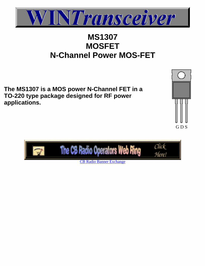
MS1307MOSFET
N-Channel Power MOS-FET
The MS1307 is a MOS power N-Channel FET in aTO-220 type package designed for RF powerapplications.
G D S
CB Radio Banner Exchange
Transistor Database
CB Radio Banner Exchange
2N109 GE-P 35V 0.15A 0.165W | 2N1304 GE-N 25V 0.3A 0.15W 10MHz 2N1305 GE-P 30V 0.3A 0.15W 5MHz | 2N1307 GE-P 30V 0.3A 0.15W B>60 2N1613 SI-N 75V 1A 0.8W 60MHz | 2N1711 SI-N 75V 1A 0.8W 70MHz 2N1893 SI-N 120V 0.5A 0.8W | 2N2102 SI-N 120V 1A 1W <120MHz 2N2148 GE-P 60V 5A 12.5W | 2N2165 SI-P 30V 50mA 0.15W 18MHz 2N2166 SI-P 15V 50mA 0.15W 10MHz | 2N2219A SI-N 40V 0.8A 0.8W 250MHz 2N2222A SI-N 40V 0.8A 0.5W 300MHz | 2N2223 2xSI-N 100V 0.5A 0.6W >50 2N2223A 2xSI-N 100V 0.5A 0.6W >50 | 2N2243A SI-N 120V 1A 0.8W 50MHz 2N2369A SI-N 40V 0.2A .36W 12/18ns | 2N2857 SI-N 30V 40mA 0.2W >1GHz 2N2894 SI-P 12V 0.2A 1.2W 60/90ns | 2N2905A SI-P 60V 0.6A 0.6W 45/100 2N2906A SI-P 60V 0.6A 0.4W 45/100 | 2N2907A SI-P 60V 0.6A 0.4W 45/100 2N2917 SI-N 45V 0.03A >60Mz | 2N2926 SI-N 25V 0.1A 0.2W 300MHz 2N2955 GE-P 40V 0.1A 0.15W 200MHz | 2N3019 SI-N 140V 1A 0.8W 100MHz 2N3053 SI-N 60V 0.7A 5W 100MHz | 2N3054 SI-N 90V 4A 25W 3MHz 2N3055 SI-N 100V 15A 115W 800kHz | 2N3055 SI-N 100V 15A 115W 800kHz 2N3055H SI-N 100V 15A 115W 800kHz | 2N3251 SI-P 50V 0.2A 0.36W 2N3375 SI-N 40V 0.5A 11.6W 500MHz | 2N3439 SI-N 450V 1A 10W 15MHz 2N3440 SI-N 300V 1A 10W 15MHz | 2N3441 SI-N 160V 3A 25W POWER 2N3442 SI-N 160V 10A 117W 0.8MHz | 2N3495 SI-P 120V 0.1A 0.6W>150MHz 2N3502 SI-P 45V 0.6A 0.7W 200MHz | 2N3553 SI-N 65V 0.35A 7W 500MHz 2N3571 SI-N 30V 0.05A 0.2W 1.4GHz | 2N3583 SI-N 250/175V 2A 35W>10MHz 2N3632 SI-N 40V 0.25A 23W 400MHz | 2N3646 SI-N 40V 0.2A 0.2W 2N3700 SI-N 140V 1A 0.5W 200MHz | 2N3707 SI-N 30V 0.03A 0.36W100MHz 2N3708 SI-N 30V 0.03A 0.36W 80MHz | 2N3716 SI-N 100V 10A 150W 4MHz 2N3725 SI-N 80V 0.5A 1W 35/60ns | 2N3740 SI-P 60V 4A 25W >4MHz 2N3741 SI-N 80V 4A 25W >4MHz | 2N3742 SI-N 300V 0.05A 1W >30MHz 2N3767 SI-N 100V 4A 20W >10MHz | 2N3771 SI-N 50V 30A 150W POWER 2N3772 SI-N 100V 20A 150W POWER | 2N3773 SI-N 160V 16A 150W POWER 2N3792 SI-P 80V 10A 150W 4MHz | 2N3819 N-FET 25V 20mA 0.36W 2N3820 P-FET 20V 15mA 0.36W | 2N3821 N-FET 50V 2.5mA 0.3W 2N3824 N-FET 50V 10mA 0.3W <250E | 2N3866 SI-N 55V 0.4A 1W 175MHz 2N3904 SI-N 60V 0.2A .35W 300MHz | 2N3906 SI-P 40V 0.2A .35W 250MHz 2N3909 P-FET 20V 10MA 0.3W | 2N3958 N-FET 50V 5mA 0.25W
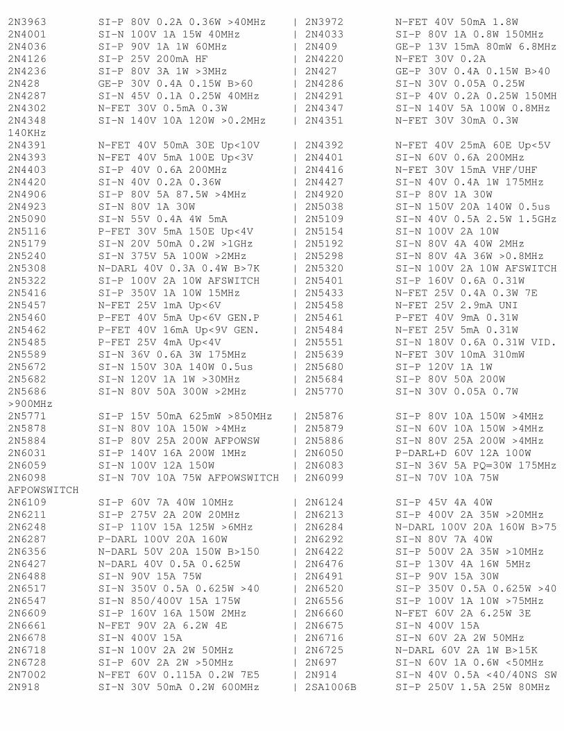
2N3963 SI-P 80V 0.2A 0.36W >40MHz | 2N3972 N-FET 40V 50mA 1.8W 2N4001 SI-N 100V 1A 15W 40MHz | 2N4033 SI-P 80V 1A 0.8W 150MHz 2N4036 SI-P 90V 1A 1W 60MHz | 2N409 GE-P 13V 15mA 80mW 6.8MHz 2N4126 SI-P 25V 200mA HF | 2N4220 N-FET 30V 0.2A 2N4236 SI-P 80V 3A 1W >3MHz | 2N427 GE-P 30V 0.4A 0.15W B>40 2N428 GE-P 30V 0.4A 0.15W B>60 | 2N4286 SI-N 30V 0.05A 0.25W 2N4287 SI-N 45V 0.1A 0.25W 40MHz | 2N4291 SI-P 40V 0.2A 0.25W 150MH 2N4302 N-FET 30V 0.5mA 0.3W | 2N4347 SI-N 140V 5A 100W 0.8MHz 2N4348 SI-N 140V 10A 120W >0.2MHz | 2N4351 N-FET 30V 30mA 0.3W140KHz 2N4391 N-FET 40V 50mA 30E Up<10V | 2N4392 N-FET 40V 25mA 60E Up<5V 2N4393 N-FET 40V 5mA 100E Up<3V | 2N4401 SI-N 60V 0.6A 200MHz 2N4403 SI-P 40V 0.6A 200MHz | 2N4416 N-FET 30V 15mA VHF/UHF 2N4420 SI-N 40V 0.2A 0.36W | 2N4427 SI-N 40V 0.4A 1W 175MHz 2N4906 SI-P 80V 5A 87.5W >4MHz | 2N4920 SI-P 80V 1A 30W 2N4923 SI-N 80V 1A 30W | 2N5038 SI-N 150V 20A 140W 0.5us 2N5090 SI-N 55V 0.4A 4W 5mA | 2N5109 SI-N 40V 0.5A 2.5W 1.5GHz 2N5116 P-FET 30V 5mA 150E Up<4V | 2N5154 SI-N 100V 2A 10W 2N5179 SI-N 20V 50mA 0.2W >1GHz | 2N5192 SI-N 80V 4A 40W 2MHz 2N5240 SI-N 375V 5A 100W >2MHz | 2N5298 SI-N 80V 4A 36W >0.8MHz 2N5308 N-DARL 40V 0.3A 0.4W B>7K | 2N5320 SI-N 100V 2A 10W AFSWITCH 2N5322 SI-P 100V 2A 10W AFSWITCH | 2N5401 SI-P 160V 0.6A 0.31W 2N5416 SI-P 350V 1A 10W 15MHz | 2N5433 N-FET 25V 0.4A 0.3W 7E 2N5457 N-FET 25V 1mA Up<6V | 2N5458 N-FET 25V 2.9mA UNI 2N5460 P-FET 40V 5mA Up<6V GEN.P | 2N5461 P-FET 40V 9mA 0.31W 2N5462 P-FET 40V 16mA Up<9V GEN. | 2N5484 N-FET 25V 5mA 0.31W 2N5485 P-FET 25V 4mA Up<4V | 2N5551 SI-N 180V 0.6A 0.31W VID. 2N5589 SI-N 36V 0.6A 3W 175MHz | 2N5639 N-FET 30V 10mA 310mW 2N5672 SI-N 150V 30A 140W 0.5us | 2N5680 SI-P 120V 1A 1W 2N5682 SI-N 120V 1A 1W >30MHz | 2N5684 SI-P 80V 50A 200W 2N5686 SI-N 80V 50A 300W >2MHz | 2N5770 SI-N 30V 0.05A 0.7W>900MHz 2N5771 SI-P 15V 50mA 625mW >850MHz | 2N5876 SI-P 80V 10A 150W >4MHz 2N5878 SI-N 80V 10A 150W >4MHz | 2N5879 SI-N 60V 10A 150W >4MHz 2N5884 SI-P 80V 25A 200W AFPOWSW | 2N5886 SI-N 80V 25A 200W >4MHz 2N6031 SI-P 140V 16A 200W 1MHz | 2N6050 P-DARL+D 60V 12A 100W 2N6059 SI-N 100V 12A 150W | 2N6083 SI-N 36V 5A PQ=30W 175MHz 2N6098 SI-N 70V 10A 75W AFPOWSWITCH | 2N6099 SI-N 70V 10A 75WAFPOWSWITCH2N6109 SI-P 60V 7A 40W 10MHz | 2N6124 SI-P 45V 4A 40W 2N6211 SI-P 275V 2A 20W 20MHz | 2N6213 SI-P 400V 2A 35W >20MHz 2N6248 SI-P 110V 15A 125W >6MHz | 2N6284 N-DARL 100V 20A 160W B>75 2N6287 P-DARL 100V 20A 160W | 2N6292 SI-N 80V 7A 40W 2N6356 N-DARL 50V 20A 150W B>150 | 2N6422 SI-P 500V 2A 35W >10MHz 2N6427 N-DARL 40V 0.5A 0.625W | 2N6476 SI-P 130V 4A 16W 5MHz 2N6488 SI-N 90V 15A 75W | 2N6491 SI-P 90V 15A 30W 2N6517 SI-N 350V 0.5A 0.625W >40 | 2N6520 SI-P 350V 0.5A 0.625W >40 2N6547 SI-N 850/400V 15A 175W | 2N6556 SI-P 100V 1A 10W >75MHz 2N6609 SI-P 160V 16A 150W 2MHz | 2N6660 N-FET 60V 2A 6.25W 3E 2N6661 N-FET 90V 2A 6.2W 4E | 2N6675 SI-N 400V 15A 2N6678 SI-N 400V 15A | 2N6716 SI-N 60V 2A 2W 50MHz 2N6718 SI-N 100V 2A 2W 50MHz | 2N6725 N-DARL 60V 2A 1W B>15K 2N6728 SI-P 60V 2A 2W >50MHz | 2N697 SI-N 60V 1A 0.6W <50MHz 2N7002 N-FET 60V 0.115A 0.2W 7E5 | 2N914 SI-N 40V 0.5A <40/40NS SW 2N918 SI-N 30V 50mA 0.2W 600MHz | 2SA1006B SI-P 250V 1.5A 25W 80MHz

2SA1009 SI-P 350V 2A 15W | 2SA1011 SI-P 160V 1.5A 25W 120MHz 2SA1013 SI-P 160V 1A 0.9W 50MHz | 2SA1015 SI-P 50V 0.15A 0.4W 80MHz 2SA1016 SI-P 100V 0.05A 0.4W 110MHz | 2SA1017 SI-P 120V 50mA 0.5W110MHz 2SA1018 SI-P 250V 70mA 0.75W >50MHz | 2SA1020 SI-P 50V 2A 0.9W 100MHz 2SA1027 SI-P 50V 0.2A 0.25W 100MHz | 2SA1029 SI-P 30V 0.1A 0.2W 280MHz 2SA1034 SI-P 35V 50mA 0.2W 200MHz | 2SA1037 SI-P 50V 0.4A 140MHz FR 2SA1048 SI-P 50V 0.15A 0.2W 80MHz | 2SA1049 SI-P 120V 0.1A 0.2W100MHz 2SA1061 SI-P 100V 6A 70W 15MHz | 2SA1062 SI-N 120V 7A 80W 15MHz 2SA1065 SI-P 150V 10A 120W 50MHz | 2SA1084 SI-P 90V 0.1A 0.4W 90MHz 2SA1103 SI-P 100V 7A 70W 20MHz | 2SA1106 SI-P 140V 10A 100W 20MHz 2SA1110 SI-P 120V 0.5A 5W 250MHz | 2SA1111 SI-P 150V 1A 20W 200MHz 2SA1112 SI-P 180V 1A 20W 200MHz | 2SA1115 SI-P 50V 0.2A 200MHz UNI 2SA1120 SI-P 35V 5A 170MHz | 2SA1123 SI-P 150V 50mA 0.75W200MHz 2SA1124 SI-P 150V 50mA 1W 200MHz | 2SA1127 SI-P 60V 0.1A 0.4W 200MHz 2SA1141 SI-P 115V 10A 100W 90MHz | 2SA1142 SI-P 180V 0.1A 8W 180MHz 2SA1145 SI-P 150V 50mA 0.8W 200MHz | 2SA1150 SI-P 35V 0.8A 0.3W 120MHz 2SA1156 SI-P 400V 0.5A 10W POWER | 2SA1160 SI-P 20V 2A 0.9W 150MHz 2SA1163 SI-P 120V 0.1A 100MHz | 2SA1170 SI-P 200V 17A 200W 20MHz 2SA1185 SI-P 50V 7A 60W 100MHz | 2SA1186 SI-P 150V 10A 100W 2SA1200 SI-P 150V 50mA 0.5W 120MHz | 2SA1201 SI-P 120V 0.8A 0.5W120MHz 2SA1206 SI-P 15V 0.05A 0.6W | 2SA1207 SI-P 180V 70mA 0.6W150MHz 2SA1208 SI-P 180V 0.07A 0.9W | 2SA1209 SI-P 180V 0.14A 10W 2SA1210 SI-P 200V 0.14A 10W | 2SA1213 SI-P 50V 2A 0.5W 120MHz 2SA1215 SI-P 160V 15A 150W 50MHz | 2SA1216 SI-P 180V 17A 200W 40MHz 2SA1220A SI-P 120V 1.2A 20W 160MHz | 2SA1221 SI-P 160V 0.5A 1W 45MHz 2SA1225 SI-P 160V 1.5A 15W 100MHz | 2SA1227A SI-P 140V 12A 120W 60MHz 2SA1232 SI-P 130V 10A 100W 60MHz | 2SA1241 SI-P 50V 2A 10W 100MHz 2SA1242 SI-P 35V 5A 1W 170MHz | 2SA1244 SI-P 60V 5A 20W 60MHz 2SA1249 SI-P 180V 1.5A 10W 120MHz | 2SA1261 SI-P 100V 10A 60W POWER 2SA1262 SI-P 60V 4A 30W 15MHz | 2SA1264N SI-P 120V 8A 80W 30MHz 2SA1265N SI-P 140V 10A 100W 30MHz | 2SA1266 SI-P 50V 0.15A 0.4W POWER 2SA1268 SI-N 120V 0.1A 0.3W 100MHz | 2SA1270 SI-P 35V 0.5A 0.5W200MHz 2SA1271 SI-P 30V 0.8A 0.6W 120MHz | 2SA1275 SI-P 160V 1A 0.9W 20MHz 2SA1282 SI-P 20V 2A 0.9W 80MHz | 2SA1283 SI-P 60V 1A 0.9W 85MHz 2SA1286 SI-P 30V 1.5A 0.9W 90MHz | 2SA1287 SI-P 50V 1A 0.9W 90MHz 2SA1292 SI-P 80V 15A 70W 100MHz | 2SA1293 SI-P 100V 5A 30W 0.2us 2SA1294 SI-P 230V 15A 130W | 2SA1295 SI-P 230V 17A 200W 35MHz 2SA1296 SI-P 20V 2A 0.75W 120MHz | 2SA1298 SI-P 30V 0.8A 0.2W 120MHz 2SA1300 SI-P 10V 2A 0.75W 140MHz | 2SA1302 SI-P 200V 15A 150W 25MHz 2SA1303 SI-P 150V 14A 125W 50MHz | 2SA1306 SI-P 160V 1.5A 20W 2SA1306A SI-P 180V 1.5A 20W 100MHz | 2SA1307 SI-P 60V 5A 20W 0.1us 2SA1309 SI-P 30V 0.1A 0.3W 80MHz | 2SA1310 SI-P 60V 0.1A 0.3W 200MHz 2SA1315 SI-P 80V 2A 0.9W 0.2us | 2SA1316 SI-P 80V 0.1A 0.4W 50MHz 2SA1317 SI-P 60V 0.2A 0.3W 200MHz | 2SA1318 SI-P 60V 0.2A 0.5W 200MHz 2SA1319 SI-P 180V 0.7A 0.7W 120MHz | 2SA1321 SI-P 250V 50mA 0.9W100MHz 2SA1328 SI-P 60V 12A 40W 0.3us | 2SA1329 SI-P 80V 12A 40W 0.3us 2SA1345 SI-N 50V 0.1A 0.3W 250MHz | 2SA1346 SI-P 50V 0.1A 200MHz 2SA1348 SI-P 50V 0.1A 200MHz | 2SA1349 P-ARRAY 80V 0.1A 0.4W 170
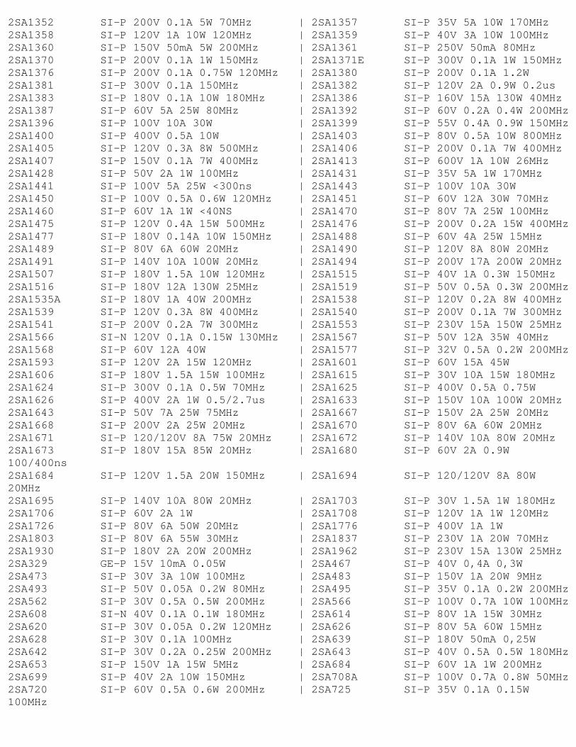
2SA1352 SI-P 200V 0.1A 5W 70MHz | 2SA1357 SI-P 35V 5A 10W 170MHz 2SA1358 SI-P 120V 1A 10W 120MHz | 2SA1359 SI-P 40V 3A 10W 100MHz 2SA1360 SI-P 150V 50mA 5W 200MHz | 2SA1361 SI-P 250V 50mA 80MHz 2SA1370 SI-P 200V 0.1A 1W 150MHz | 2SA1371E SI-P 300V 0.1A 1W 150MHz 2SA1376 SI-P 200V 0.1A 0.75W 120MHz | 2SA1380 SI-P 200V 0.1A 1.2W 2SA1381 SI-P 300V 0.1A 150MHz | 2SA1382 SI-P 120V 2A 0.9W 0.2us 2SA1383 SI-P 180V 0.1A 10W 180MHz | 2SA1386 SI-P 160V 15A 130W 40MHz 2SA1387 SI-P 60V 5A 25W 80MHz | 2SA1392 SI-P 60V 0.2A 0.4W 200MHz 2SA1396 SI-P 100V 10A 30W | 2SA1399 SI-P 55V 0.4A 0.9W 150MHz 2SA1400 SI-P 400V 0.5A 10W | 2SA1403 SI-P 80V 0.5A 10W 800MHz 2SA1405 SI-P 120V 0.3A 8W 500MHz | 2SA1406 SI-P 200V 0.1A 7W 400MHz 2SA1407 SI-P 150V 0.1A 7W 400MHz | 2SA1413 SI-P 600V 1A 10W 26MHz 2SA1428 SI-P 50V 2A 1W 100MHz | 2SA1431 SI-P 35V 5A 1W 170MHz 2SA1441 SI-P 100V 5A 25W <300ns | 2SA1443 SI-P 100V 10A 30W 2SA1450 SI-P 100V 0.5A 0.6W 120MHz | 2SA1451 SI-P 60V 12A 30W 70MHz 2SA1460 SI-P 60V 1A 1W <40NS | 2SA1470 SI-P 80V 7A 25W 100MHz 2SA1475 SI-P 120V 0.4A 15W 500MHz | 2SA1476 SI-P 200V 0.2A 15W 400MHz 2SA1477 SI-P 180V 0.14A 10W 150MHz | 2SA1488 SI-P 60V 4A 25W 15MHz 2SA1489 SI-P 80V 6A 60W 20MHz | 2SA1490 SI-P 120V 8A 80W 20MHz 2SA1491 SI-P 140V 10A 100W 20MHz | 2SA1494 SI-P 200V 17A 200W 20MHz 2SA1507 SI-P 180V 1.5A 10W 120MHz | 2SA1515 SI-P 40V 1A 0.3W 150MHz 2SA1516 SI-P 180V 12A 130W 25MHz | 2SA1519 SI-P 50V 0.5A 0.3W 200MHz 2SA1535A SI-P 180V 1A 40W 200MHz | 2SA1538 SI-P 120V 0.2A 8W 400MHz 2SA1539 SI-P 120V 0.3A 8W 400MHz | 2SA1540 SI-P 200V 0.1A 7W 300MHz 2SA1541 SI-P 200V 0.2A 7W 300MHz | 2SA1553 SI-P 230V 15A 150W 25MHz 2SA1566 SI-N 120V 0.1A 0.15W 130MHz | 2SA1567 SI-P 50V 12A 35W 40MHz 2SA1568 SI-P 60V 12A 40W | 2SA1577 SI-P 32V 0.5A 0.2W 200MHz 2SA1593 SI-P 120V 2A 15W 120MHz | 2SA1601 SI-P 60V 15A 45W 2SA1606 SI-P 180V 1.5A 15W 100MHz | 2SA1615 SI-P 30V 10A 15W 180MHz 2SA1624 SI-P 300V 0.1A 0.5W 70MHz | 2SA1625 SI-P 400V 0.5A 0.75W 2SA1626 SI-P 400V 2A 1W 0.5/2.7us | 2SA1633 SI-P 150V 10A 100W 20MHz 2SA1643 SI-P 50V 7A 25W 75MHz | 2SA1667 SI-P 150V 2A 25W 20MHz 2SA1668 SI-P 200V 2A 25W 20MHz | 2SA1670 SI-P 80V 6A 60W 20MHz 2SA1671 SI-P 120/120V 8A 75W 20MHz | 2SA1672 SI-P 140V 10A 80W 20MHz 2SA1673 SI-P 180V 15A 85W 20MHz | 2SA1680 SI-P 60V 2A 0.9W100/400ns 2SA1684 SI-P 120V 1.5A 20W 150MHz | 2SA1694 SI-P 120/120V 8A 80W20MHz 2SA1695 SI-P 140V 10A 80W 20MHz | 2SA1703 SI-P 30V 1.5A 1W 180MHz 2SA1706 SI-P 60V 2A 1W | 2SA1708 SI-P 120V 1A 1W 120MHz 2SA1726 SI-P 80V 6A 50W 20MHz | 2SA1776 SI-P 400V 1A 1W 2SA1803 SI-P 80V 6A 55W 30MHz | 2SA1837 SI-P 230V 1A 20W 70MHz 2SA1930 SI-P 180V 2A 20W 200MHz | 2SA1962 SI-P 230V 15A 130W 25MHz 2SA329 GE-P 15V 10mA 0.05W | 2SA467 SI-P 40V 0,4A 0,3W 2SA473 SI-P 30V 3A 10W 100MHz | 2SA483 SI-P 150V 1A 20W 9MHz 2SA493 SI-P 50V 0.05A 0.2W 80MHz | 2SA495 SI-P 35V 0.1A 0.2W 200MHz 2SA562 SI-P 30V 0.5A 0.5W 200MHz | 2SA566 SI-P 100V 0.7A 10W 100MHz 2SA608 SI-N 40V 0.1A 0.1W 180MHz | 2SA614 SI-P 80V 1A 15W 30MHz 2SA620 SI-P 30V 0.05A 0.2W 120MHz | 2SA626 SI-P 80V 5A 60W 15MHz 2SA628 SI-P 30V 0.1A 100MHz | 2SA639 SI-P 180V 50mA 0,25W 2SA642 SI-P 30V 0.2A 0.25W 200MHz | 2SA643 SI-P 40V 0.5A 0.5W 180MHz 2SA653 SI-P 150V 1A 15W 5MHz | 2SA684 SI-P 60V 1A 1W 200MHz 2SA699 SI-P 40V 2A 10W 150MHz | 2SA708A SI-P 100V 0.7A 0.8W 50MHz 2SA720 SI-P 60V 0.5A 0.6W 200MHz | 2SA725 SI-P 35V 0.1A 0.15W100MHz
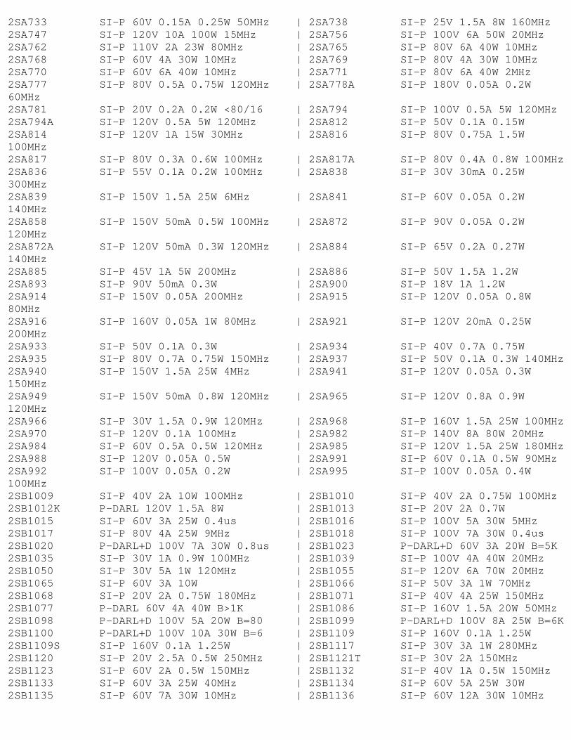
2SA733 SI-P 60V 0.15A 0.25W 50MHz | 2SA738 SI-P 25V 1.5A 8W 160MHz 2SA747 SI-P 120V 10A 100W 15MHz | 2SA756 SI-P 100V 6A 50W 20MHz 2SA762 SI-P 110V 2A 23W 80MHz | 2SA765 SI-P 80V 6A 40W 10MHz 2SA768 SI-P 60V 4A 30W 10MHz | 2SA769 SI-P 80V 4A 30W 10MHz 2SA770 SI-P 60V 6A 40W 10MHz | 2SA771 SI-P 80V 6A 40W 2MHz 2SA777 SI-P 80V 0.5A 0.75W 120MHz | 2SA778A SI-P 180V 0.05A 0.2W60MHz 2SA781 SI-P 20V 0.2A 0.2W <80/16 | 2SA794 SI-P 100V 0.5A 5W 120MHz 2SA794A SI-P 120V 0.5A 5W 120MHz | 2SA812 SI-P 50V 0.1A 0.15W 2SA814 SI-P 120V 1A 15W 30MHz | 2SA816 SI-P 80V 0.75A 1.5W100MHz 2SA817 SI-P 80V 0.3A 0.6W 100MHz | 2SA817A SI-P 80V 0.4A 0.8W 100MHz 2SA836 SI-P 55V 0.1A 0.2W 100MHz | 2SA838 SI-P 30V 30mA 0.25W300MHz 2SA839 SI-P 150V 1.5A 25W 6MHz | 2SA841 SI-P 60V 0.05A 0.2W140MHz 2SA858 SI-P 150V 50mA 0.5W 100MHz | 2SA872 SI-P 90V 0.05A 0.2W120MHz 2SA872A SI-P 120V 50mA 0.3W 120MHz | 2SA884 SI-P 65V 0.2A 0.27W140MHz 2SA885 SI-P 45V 1A 5W 200MHz | 2SA886 SI-P 50V 1.5A 1.2W 2SA893 SI-P 90V 50mA 0.3W | 2SA900 SI-P 18V 1A 1.2W 2SA914 SI-P 150V 0.05A 200MHz | 2SA915 SI-P 120V 0.05A 0.8W80MHz 2SA916 SI-P 160V 0.05A 1W 80MHz | 2SA921 SI-P 120V 20mA 0.25W200MHz 2SA933 SI-P 50V 0.1A 0.3W | 2SA934 SI-P 40V 0.7A 0.75W 2SA935 SI-P 80V 0.7A 0.75W 150MHz | 2SA937 SI-P 50V 0.1A 0.3W 140MHz 2SA940 SI-P 150V 1.5A 25W 4MHz | 2SA941 SI-P 120V 0.05A 0.3W150MHz 2SA949 SI-P 150V 50mA 0.8W 120MHz | 2SA965 SI-P 120V 0.8A 0.9W120MHz 2SA966 SI-P 30V 1.5A 0.9W 120MHz | 2SA968 SI-P 160V 1.5A 25W 100MHz 2SA970 SI-P 120V 0.1A 100MHz | 2SA982 SI-P 140V 8A 80W 20MHz 2SA984 SI-P 60V 0.5A 0.5W 120MHz | 2SA985 SI-P 120V 1.5A 25W 180MHz 2SA988 SI-P 120V 0.05A 0.5W | 2SA991 SI-P 60V 0.1A 0.5W 90MHz 2SA992 SI-P 100V 0.05A 0.2W | 2SA995 SI-P 100V 0.05A 0.4W100MHz 2SB1009 SI-P 40V 2A 10W 100MHz | 2SB1010 SI-P 40V 2A 0.75W 100MHz 2SB1012K P-DARL 120V 1.5A 8W | 2SB1013 SI-P 20V 2A 0.7W 2SB1015 SI-P 60V 3A 25W 0.4us | 2SB1016 SI-P 100V 5A 30W 5MHz 2SB1017 SI-P 80V 4A 25W 9MHz | 2SB1018 SI-P 100V 7A 30W 0.4us 2SB1020 P-DARL+D 100V 7A 30W 0.8us | 2SB1023 P-DARL+D 60V 3A 20W B=5K 2SB1035 SI-P 30V 1A 0.9W 100MHz | 2SB1039 SI-P 100V 4A 40W 20MHz 2SB1050 SI-P 30V 5A 1W 120MHz | 2SB1055 SI-P 120V 6A 70W 20MHz 2SB1065 SI-P 60V 3A 10W | 2SB1066 SI-P 50V 3A 1W 70MHz 2SB1068 SI-P 20V 2A 0.75W 180MHz | 2SB1071 SI-P 40V 4A 25W 150MHz 2SB1077 P-DARL 60V 4A 40W B>1K | 2SB1086 SI-P 160V 1.5A 20W 50MHz 2SB1098 P-DARL+D 100V 5A 20W B=80 | 2SB1099 P-DARL+D 100V 8A 25W B=6K 2SB1100 P-DARL+D 100V 10A 30W B=6 | 2SB1109 SI-P 160V 0.1A 1.25W 2SB1109S SI-P 160V 0.1A 1.25W | 2SB1117 SI-P 30V 3A 1W 280MHz 2SB1120 SI-P 20V 2.5A 0.5W 250MHz | 2SB1121T SI-P 30V 2A 150MHz 2SB1123 SI-P 60V 2A 0.5W 150MHz | 2SB1132 SI-P 40V 1A 0.5W 150MHz 2SB1133 SI-P 60V 3A 25W 40MHz | 2SB1134 SI-P 60V 5A 25W 30W 2SB1135 SI-P 60V 7A 30W 10MHz | 2SB1136 SI-P 60V 12A 30W 10MHz
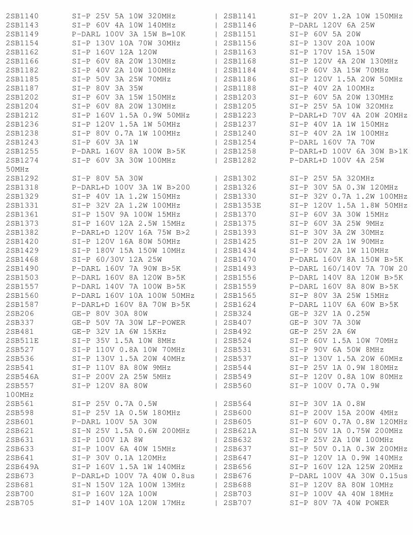
2SB1140 SI-P 25V 5A 10W 320MHz | 2SB1141 SI-P 20V 1.2A 10W 150MHz 2SB1143 SI-P 60V 4A 10W 140MHz | 2SB1146 P-DARL 120V 6A 25W 2SB1149 P-DARL 100V 3A 15W B=10K | 2SB1151 SI-P 60V 5A 20W 2SB1154 SI-P 130V 10A 70W 30MHz | 2SB1156 SI-P 130V 20A 100W 2SB1162 SI-P 160V 12A 120W | 2SB1163 SI-P 170V 15A 150W 2SB1166 SI-P 60V 8A 20W 130MHz | 2SB1168 SI-P 120V 4A 20W 130MHz 2SB1182 SI-P 40V 2A 10W 100MHz | 2SB1184 SI-P 60V 3A 15W 70MHz 2SB1185 SI-P 50V 3A 25W 70MHz | 2SB1186 SI-P 120V 1.5A 20W 50MHz 2SB1187 SI-P 80V 3A 35W | 2SB1188 SI-P 40V 2A 100MHz 2SB1202 SI-P 60V 3A 15W 150MHz | 2SB1203 SI-P 60V 5A 20W 130MHz 2SB1204 SI-P 60V 8A 20W 130MHz | 2SB1205 SI-P 25V 5A 10W 320MHz 2SB1212 SI-P 160V 1.5A 0.9W 50MHz | 2SB1223 P-DARL+D 70V 4A 20W 20MHz 2SB1236 SI-P 120V 1.5A 1W 50MHz | 2SB1237 SI-P 40V 1A 1W 150MHz 2SB1238 SI-P 80V 0.7A 1W 100MHz | 2SB1240 SI-P 40V 2A 1W 100MHz 2SB1243 SI-P 60V 3A 1W | 2SB1254 P-DARL 160V 7A 70W 2SB1255 P-DARL 160V 8A 100W B>5K | 2SB1258 P-DARL+D 100V 6A 30W B>1K 2SB1274 SI-P 60V 3A 30W 100MHz | 2SB1282 P-DARL+D 100V 4A 25W50MHz 2SB1292 SI-P 80V 5A 30W | 2SB1302 SI-P 25V 5A 320MHz 2SB1318 P-DARL+D 100V 3A 1W B>200 | 2SB1326 SI-P 30V 5A 0.3W 120MHz 2SB1329 SI-P 40V 1A 1.2W 150MHz | 2SB1330 SI-P 32V 0.7A 1.2W 100MHz 2SB1331 SI-P 32V 2A 1.2W 100MHz | 2SB1353E SI-P 120V 1.5A 1.8W 50MHz 2SB1361 SI-P 150V 9A 100W 15MHz | 2SB1370 SI-P 60V 3A 30W 15MHz 2SB1373 SI-P 160V 12A 2.5W 15MHz | 2SB1375 SI-P 60V 3A 25W 9MHz 2SB1382 P-DARL+D 120V 16A 75W B>2 | 2SB1393 SI-P 30V 3A 2W 30MHz 2SB1420 SI-P 120V 16A 80W 50MHz | 2SB1425 SI-P 20V 2A 1W 90MHz 2SB1429 SI-P 180V 15A 150W 10MHz | 2SB1434 SI-P 50V 2A 1W 110MHz 2SB1468 SI-P 60/30V 12A 25W | 2SB1470 P-DARL 160V 8A 150W B>5K 2SB1490 P-DARL 160V 7A 90W B>5K | 2SB1493 P-DARL 160/140V 7A 70W 20 2SB1503 P-DARL 160V 8A 120W B>5K | 2SB1556 P-DARL 140V 8A 120W B>5K 2SB1557 P-DARL 140V 7A 100W B>5K | 2SB1559 P-DARL 160V 8A 80W B>5K 2SB1560 P-DARL 160V 10A 100W 50MHz | 2SB1565 SI-P 80V 3A 25W 15MHz 2SB1587 P-DARL+D 160V 8A 70W B>5K | 2SB1624 P-DARL 110V 6A 60W B>5K 2SB206 GE-P 80V 30A 80W | 2SB324 GE-P 32V 1A 0.25W 2SB337 GE-P 50V 7A 30W LF-POWER | 2SB407 GE-P 30V 7A 30W 2SB481 GE-P 32V 1A 6W 15KHz | 2SB492 GE-P 25V 2A 6W 2SB511E SI-P 35V 1.5A 10W 8MHz | 2SB524 SI-P 60V 1.5A 10W 70MHz 2SB527 SI-P 110V 0.8A 10W 70MHz | 2SB531 SI-P 90V 6A 50W 8MHz 2SB536 SI-P 130V 1.5A 20W 40MHz | 2SB537 SI-P 130V 1.5A 20W 60MHz 2SB541 SI-P 110V 8A 80W 9MHz | 2SB544 SI-P 25V 1A 0.9W 180MHz 2SB546A SI-P 200V 2A 25W 5MHz | 2SB549 SI-P 120V 0.8A 10W 80MHz 2SB557 SI-P 120V 8A 80W | 2SB560 SI-P 100V 0.7A 0.9W100MHz 2SB561 SI-P 25V 0.7A 0.5W | 2SB564 SI-P 30V 1A 0.8W 2SB598 SI-P 25V 1A 0.5W 180MHz | 2SB600 SI-P 200V 15A 200W 4MHz 2SB601 P-DARL 100V 5A 30W | 2SB605 SI-P 60V 0.7A 0.8W 120MHz 2SB621 SI-N 25V 1.5A 0.6W 200MHz | 2SB621A SI-N 50V 1A 0.75W 200MHz 2SB631 SI-P 100V 1A 8W | 2SB632 SI-P 25V 2A 10W 100MHz 2SB633 SI-P 100V 6A 40W 15MHz | 2SB637 SI-P 50V 0.1A 0.3W 200MHz 2SB641 SI-P 30V 0.1A 120MHz | 2SB647 SI-P 120V 1A 0.9W 140MHz 2SB649A SI-P 160V 1.5A 1W 140MHz | 2SB656 SI-P 160V 12A 125W 20MHz 2SB673 P-DARL+D 100V 7A 40W 0.8us | 2SB676 P-DARL 100V 4A 30W 0.15us 2SB681 SI-N 150V 12A 100W 13MHz | 2SB688 SI-P 120V 8A 80W 10MHz 2SB700 SI-P 160V 12A 100W | 2SB703 SI-P 100V 4A 40W 18MHz 2SB705 SI-P 140V 10A 120W 17MHz | 2SB707 SI-P 80V 7A 40W POWER
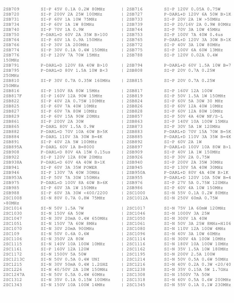
2SB709 SI-P 45V 0.1A 0.2W 80MHz | 2SB716 SI-P 120V 0.05A 0.75W 2SB720 SI-P 200V 2A 25W 100MHz | 2SB727 P-DARL+D 120V 6A 50W B>1K 2SB731 SI-P 60V 1A 10W 75MHz | 2SB733 SI-P 20V 2A 1W >50MHz 2SB734 SI-P 60V 1A 1W 80MHz | 2SB739 SI-P 20/16V 2A 0.9W 80MHz 2SB740 SI-P 70V 1A 0.9W | 2SB744 SI-P 70V 3A 10W 45MHz 2SB750 P-DARL+D 60V 2A 35W B>100 | 2SB753 SI-P 100V 7A 40W 0.4us 2SB764 SI-P 60V 1A 0.9A 150MHz | 2SB765 P-DARL+D 120V 3A 30W B>1K 2SB766 SI-P 30V 1A 200MHz | 2SB772 SI-P 40V 3A 10W 80MHz 2SB774 SI-P 30V 0.1A 0.4W 150MHz | 2SB775 SI-P 100V 6A 60W 13MHz 2SB776 SI-P 120V 7A 70W 15MHz | 2SB788 SI-P 120V 0.02A 0.4W150MHz 2SB791 P-DARL+D 120V 8A 40W B>10 | 2SB794 P-DARL+D 60V 1.5A 10W B=7 2SB795 P-DARL+D 80V 1.5A 10W B<3 | 2SB808 SI-P 20V 0.7A 0.25W250MHz 2SB810 SI-P 30V 0.7A 0.35W 160MHz | 2SB815 SI-P 20V 0.7A 0.25W250MHz 2SB816 SI-P 150V 8A 80W 15MHz | 2SB817 SI-P 160V 12A 100W 2SB817F SI-P 160V 12A 90W 15MHz | 2SB819 SI-P 50V 1.5A 1W 150MHz 2SB822 SI-P 40V 2A 0.75W 100MHz | 2SB824 SI-P 60V 5A 30W 30 MHz 2SB825 SI-P 60V 7A 40W 10MHz | 2SB826 SI-P 60V 12A 40W 10MHz 2SB827 SI-P 60V 7A 80W 10MHz | 2SB828 SI-P 60V 12A 80W 10MHz 2SB829 SI-P 60V 15A 90W 20MHz | 2SB857 SI-P 50V 4A 40W NF/S-L 2SB861 SI-P 200V 2A 30W | 2SB863 SI-P 140V 10A 100W 15MHz 2SB865 P-DARL 80V 1.5A 0.9W | 2SB873 SI-P 30V 5A 1W 120MHz 2SB882 P-DARL+D 70V 10A 40W B>5K | 2SB883 P-DARL+D 70V 15A 70W B=5K 2SB884 P-DARL 110V 3A 30W B=4K | 2SB885 P-DARL+D 110V 3A 35W B=4K 2SB891 SI-P 40V 2A 5W 100MHz | 2SB892 SI-P 60V 2A 1W 2SB895A P-DARL 60V 1A B=8000 | 2SB897 P-DARL+D 100V 10A 80W B>1 2SB908 P-DARL+D 80V 4A 15W 0.15us | 2SB909 SI-P 40V 1A 1W 150MHz 2SB922 SI-P 120V 12A 80W 20MHz | 2SB926 SI-P 30V 2A 0.75W 2SB938A P-DARL+D 60V 4A 40W B>1K | 2SB940 SI-P 200V 2A 35W 30MHz 2SB941 SI-P 60V 3A 35W POWER | 2SB945 SI-P 130V 5A 40W 30MHz 2SB946 SI-P 130V 7A 40W 30MHz | 2SB950A P-DARL+D 80V 4A 40W B>1K 2SB953A SI-P 50V 7A 30W 150MHz | 2SB955 P-DARL+D 120V 10A 50W B=4 2SB975 P-DARL+D 100V 8A 40W B>6K | 2SB976 SI-P 27V 5A 0.75W 120MHz 2SB985 SI-P 60V 3A 1W 150MHz | 2SB986 SI-P 60V 4A 10W 150MHz 2SB988 SI-P 60V 3A 30W <400/2200 | 2SC1000 SI-N 55V 0.1A 0.2W 80MHz 2SC1008 SI-N 80V 0.7A 0.8W 75MHz | 2SC1012A SI-N 250V 60mA 0.75W>80MHz 2SC1014 SI-N 50V 1.5A 7W | 2SC1017 SI-N 75V 1A 60mW 120MHz 2SC1030 SI-N 150V 6A 50W | 2SC1046 SI-N 1000V 3A 25W 2SC1047 SI-N 30V 20mA 0.4W 650MHz | 2SC1050 SI-N 300V 1A 40W 2SC1051 SI-N 150V 7A 60W 8MHz | 2SC1061 SI-N 50V 3A 25W 8MHz=H106 2SC1070 SI-N 30V 20mA 900MHz | 2SC1080 SI-N 110V 12A 100W 4MHz 2SC109 SI-N 50V 0.6A 0.6W | 2SC1096 SI-N 40V 3A 10W 60MHz 2SC1106 SI-N 350V 2A 80W | 2SC1114 SI-N 300V 4A 100W 10MHz 2SC1115 SI-N 140V 10A 100W 10MHz | 2SC1116 SI-N 180V 10A 100W 10MHz 2SC1161 SI-P 160V 12A 120W | 2SC1162 SI-N 35V 1.5A 10W 180MHz 2SC1172 SI-N 1500V 5A 50W | 2SC1195 SI-N 200V 2.5A 100W 2SC1213C SI-N 50V 0.5A 0.4W UNI | 2SC1214 SI-N 50V 0.5A 0.6W 50MHz 2SC1215 SI-N 30V 50mA 0.4W 1.2GHZ | 2SC1216 SI-N 40V 0.2A 0.3W <20/40 2SC1226 SI-N 40/50V 2A 10W 150MHz | 2SC1238 SI-N 35V 0.15A 5W 1.7GHz 2SC1247A SI-N 50V 0.5A 0.4W 60MHz | 2SC1308 SI-N 1500V 7A 50W 2SC1312 SI-N 35V 0.1A 0.15W 100MHz | 2SC1318 SI-N 60V 0.5A 0.6W 200MHz 2SC1343 SI-N 150V 10A 100W 14MHz | 2SC1345 SI-N 55V 0.1A 0.1W 230MHz
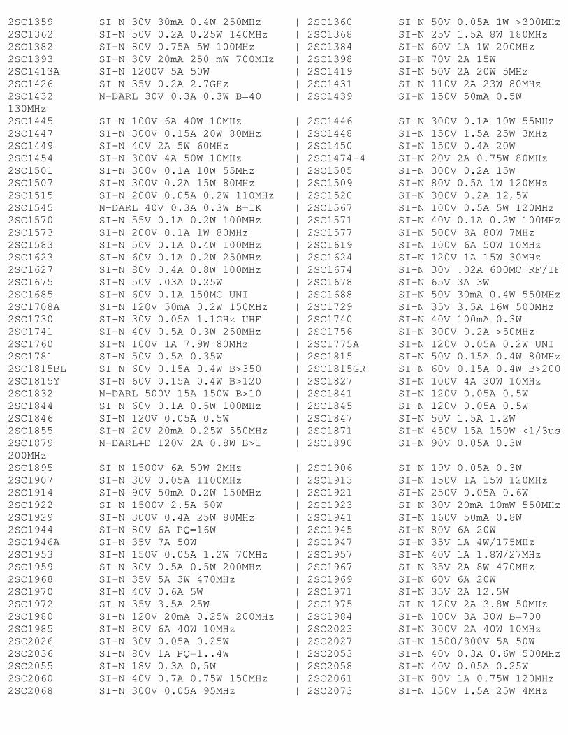
2SC1359 SI-N 30V 30mA 0.4W 250MHz | 2SC1360 SI-N 50V 0.05A 1W >300MHz 2SC1362 SI-N 50V 0.2A 0.25W 140MHz | 2SC1368 SI-N 25V 1.5A 8W 180MHz 2SC1382 SI-N 80V 0.75A 5W 100MHz | 2SC1384 SI-N 60V 1A 1W 200MHz 2SC1393 SI-N 30V 20mA 250 mW 700MHz | 2SC1398 SI-N 70V 2A 15W 2SC1413A SI-N 1200V 5A 50W | 2SC1419 SI-N 50V 2A 20W 5MHz 2SC1426 SI-N 35V 0.2A 2.7GHz | 2SC1431 SI-N 110V 2A 23W 80MHz 2SC1432 N-DARL 30V 0.3A 0.3W B=40 | 2SC1439 SI-N 150V 50mA 0.5W130MHz 2SC1445 SI-N 100V 6A 40W 10MHz | 2SC1446 SI-N 300V 0.1A 10W 55MHz 2SC1447 SI-N 300V 0.15A 20W 80MHz | 2SC1448 SI-N 150V 1.5A 25W 3MHz 2SC1449 SI-N 40V 2A 5W 60MHz | 2SC1450 SI-N 150V 0.4A 20W 2SC1454 SI-N 300V 4A 50W 10MHz | 2SC1474-4 SI-N 20V 2A 0.75W 80MHz 2SC1501 SI-N 300V 0.1A 10W 55MHz | 2SC1505 SI-N 300V 0.2A 15W 2SC1507 SI-N 300V 0.2A 15W 80MHz | 2SC1509 SI-N 80V 0.5A 1W 120MHz 2SC1515 SI-N 200V 0.05A 0.2W 110MHz | 2SC1520 SI-N 300V 0.2A 12,5W 2SC1545 N-DARL 40V 0.3A 0.3W B=1K | 2SC1567 SI-N 100V 0.5A 5W 120MHz 2SC1570 SI-N 55V 0.1A 0.2W 100MHz | 2SC1571 SI-N 40V 0.1A 0.2W 100MHz 2SC1573 SI-N 200V 0.1A 1W 80MHz | 2SC1577 SI-N 500V 8A 80W 7MHz 2SC1583 SI-N 50V 0.1A 0.4W 100MHz | 2SC1619 SI-N 100V 6A 50W 10MHz 2SC1623 SI-N 60V 0.1A 0.2W 250MHz | 2SC1624 SI-N 120V 1A 15W 30MHz 2SC1627 SI-N 80V 0.4A 0.8W 100MHz | 2SC1674 SI-N 30V .02A 600MC RF/IF 2SC1675 SI-N 50V .03A 0.25W | 2SC1678 SI-N 65V 3A 3W 2SC1685 SI-N 60V 0.1A 150MC UNI | 2SC1688 SI-N 50V 30mA 0.4W 550MHz 2SC1708A SI-N 120V 50mA 0.2W 150MHz | 2SC1729 SI-N 35V 3.5A 16W 500MHz 2SC1730 SI-N 30V 0.05A 1.1GHz UHF | 2SC1740 SI-N 40V 100mA 0.3W 2SC1741 SI-N 40V 0.5A 0.3W 250MHz | 2SC1756 SI-N 300V 0.2A >50MHz 2SC1760 SI-N 100V 1A 7.9W 80MHz | 2SC1775A SI-N 120V 0.05A 0.2W UNI 2SC1781 SI-N 50V 0.5A 0.35W | 2SC1815 SI-N 50V 0.15A 0.4W 80MHz 2SC1815BL SI-N 60V 0.15A 0.4W B>350 | 2SC1815GR SI-N 60V 0.15A 0.4W B>200 2SC1815Y SI-N 60V 0.15A 0.4W B>120 | 2SC1827 SI-N 100V 4A 30W 10MHz 2SC1832 N-DARL 500V 15A 150W B>10 | 2SC1841 SI-N 120V 0.05A 0.5W 2SC1844 SI-N 60V 0.1A 0.5W 100MHz | 2SC1845 SI-N 120V 0.05A 0.5W 2SC1846 SI-N 120V 0.05A 0.5W | 2SC1847 SI-N 50V 1.5A 1.2W 2SC1855 SI-N 20V 20mA 0.25W 550MHz | 2SC1871 SI-N 450V 15A 150W <1/3us 2SC1879 N-DARL+D 120V 2A 0.8W B>1 | 2SC1890 SI-N 90V 0.05A 0.3W200MHz 2SC1895 SI-N 1500V 6A 50W 2MHz | 2SC1906 SI-N 19V 0.05A 0.3W 2SC1907 SI-N 30V 0.05A 1100MHz | 2SC1913 SI-N 150V 1A 15W 120MHz 2SC1914 SI-N 90V 50mA 0.2W 150MHz | 2SC1921 SI-N 250V 0.05A 0.6W 2SC1922 SI-N 1500V 2.5A 50W | 2SC1923 SI-N 30V 20mA 10mW 550MHz 2SC1929 SI-N 300V 0.4A 25W 80MHz | 2SC1941 SI-N 160V 50mA 0.8W 2SC1944 SI-N 80V 6A PQ=16W | 2SC1945 SI-N 80V 6A 20W 2SC1946A SI-N 35V 7A 50W | 2SC1947 SI-N 35V 1A 4W/175MHz 2SC1953 SI-N 150V 0.05A 1.2W 70MHz | 2SC1957 SI-N 40V 1A 1.8W/27MHz 2SC1959 SI-N 30V 0.5A 0.5W 200MHz | 2SC1967 SI-N 35V 2A 8W 470MHz 2SC1968 SI-N 35V 5A 3W 470MHz | 2SC1969 SI-N 60V 6A 20W 2SC1970 SI-N 40V 0.6A 5W | 2SC1971 SI-N 35V 2A 12.5W 2SC1972 SI-N 35V 3.5A 25W | 2SC1975 SI-N 120V 2A 3.8W 50MHz 2SC1980 SI-N 120V 20mA 0.25W 200MHz | 2SC1984 SI-N 100V 3A 30W B=700 2SC1985 SI-N 80V 6A 40W 10MHz | 2SC2023 SI-N 300V 2A 40W 10MHz 2SC2026 SI-N 30V 0.05A 0.25W | 2SC2027 SI-N 1500/800V 5A 50W 2SC2036 SI-N 80V 1A PQ=1..4W | 2SC2053 SI-N 40V 0.3A 0.6W 500MHz 2SC2055 SI-N 18V 0,3A 0,5W | 2SC2058 SI-N 40V 0.05A 0.25W 2SC2060 SI-N 40V 0.7A 0.75W 150MHz | 2SC2061 SI-N 80V 1A 0.75W 120MHz 2SC2068 SI-N 300V 0.05A 95MHz | 2SC2073 SI-N 150V 1.5A 25W 4MHz
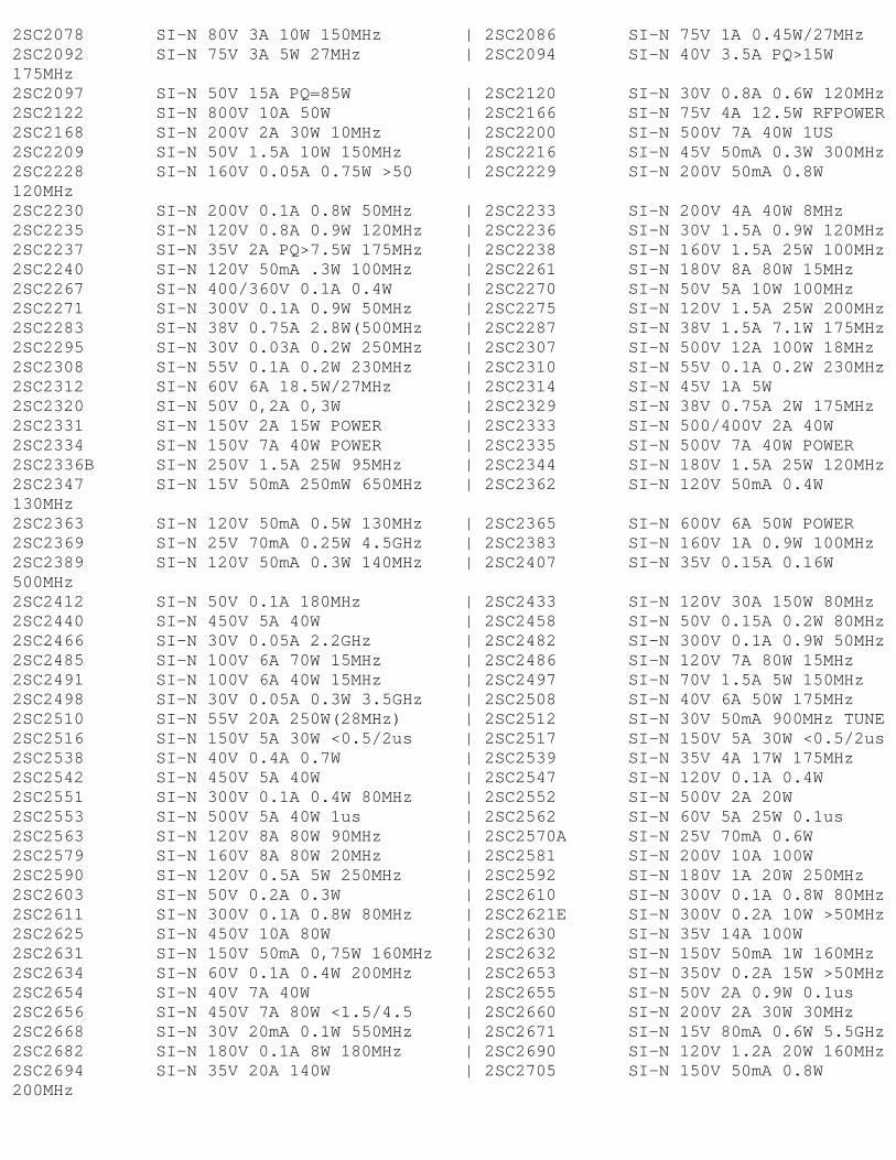
2SC2078 SI-N 80V 3A 10W 150MHz | 2SC2086 SI-N 75V 1A 0.45W/27MHz 2SC2092 SI-N 75V 3A 5W 27MHz | 2SC2094 SI-N 40V 3.5A PQ>15W175MHz 2SC2097 SI-N 50V 15A PQ=85W | 2SC2120 SI-N 30V 0.8A 0.6W 120MHz 2SC2122 SI-N 800V 10A 50W | 2SC2166 SI-N 75V 4A 12.5W RFPOWER 2SC2168 SI-N 200V 2A 30W 10MHz | 2SC2200 SI-N 500V 7A 40W 1US 2SC2209 SI-N 50V 1.5A 10W 150MHz | 2SC2216 SI-N 45V 50mA 0.3W 300MHz 2SC2228 SI-N 160V 0.05A 0.75W >50 | 2SC2229 SI-N 200V 50mA 0.8W120MHz 2SC2230 SI-N 200V 0.1A 0.8W 50MHz | 2SC2233 SI-N 200V 4A 40W 8MHz 2SC2235 SI-N 120V 0.8A 0.9W 120MHz | 2SC2236 SI-N 30V 1.5A 0.9W 120MHz 2SC2237 SI-N 35V 2A PQ>7.5W 175MHz | 2SC2238 SI-N 160V 1.5A 25W 100MHz 2SC2240 SI-N 120V 50mA .3W 100MHz | 2SC2261 SI-N 180V 8A 80W 15MHz 2SC2267 SI-N 400/360V 0.1A 0.4W | 2SC2270 SI-N 50V 5A 10W 100MHz 2SC2271 SI-N 300V 0.1A 0.9W 50MHz | 2SC2275 SI-N 120V 1.5A 25W 200MHz 2SC2283 SI-N 38V 0.75A 2.8W(500MHz | 2SC2287 SI-N 38V 1.5A 7.1W 175MHz 2SC2295 SI-N 30V 0.03A 0.2W 250MHz | 2SC2307 SI-N 500V 12A 100W 18MHz 2SC2308 SI-N 55V 0.1A 0.2W 230MHz | 2SC2310 SI-N 55V 0.1A 0.2W 230MHz 2SC2312 SI-N 60V 6A 18.5W/27MHz | 2SC2314 SI-N 45V 1A 5W 2SC2320 SI-N 50V 0,2A 0,3W | 2SC2329 SI-N 38V 0.75A 2W 175MHz 2SC2331 SI-N 150V 2A 15W POWER | 2SC2333 SI-N 500/400V 2A 40W 2SC2334 SI-N 150V 7A 40W POWER | 2SC2335 SI-N 500V 7A 40W POWER 2SC2336B SI-N 250V 1.5A 25W 95MHz | 2SC2344 SI-N 180V 1.5A 25W 120MHz 2SC2347 SI-N 15V 50mA 250mW 650MHz | 2SC2362 SI-N 120V 50mA 0.4W130MHz 2SC2363 SI-N 120V 50mA 0.5W 130MHz | 2SC2365 SI-N 600V 6A 50W POWER 2SC2369 SI-N 25V 70mA 0.25W 4.5GHz | 2SC2383 SI-N 160V 1A 0.9W 100MHz 2SC2389 SI-N 120V 50mA 0.3W 140MHz | 2SC2407 SI-N 35V 0.15A 0.16W500MHz 2SC2412 SI-N 50V 0.1A 180MHz | 2SC2433 SI-N 120V 30A 150W 80MHz 2SC2440 SI-N 450V 5A 40W | 2SC2458 SI-N 50V 0.15A 0.2W 80MHz 2SC2466 SI-N 30V 0.05A 2.2GHz | 2SC2482 SI-N 300V 0.1A 0.9W 50MHz 2SC2485 SI-N 100V 6A 70W 15MHz | 2SC2486 SI-N 120V 7A 80W 15MHz 2SC2491 SI-N 100V 6A 40W 15MHz | 2SC2497 SI-N 70V 1.5A 5W 150MHz 2SC2498 SI-N 30V 0.05A 0.3W 3.5GHz | 2SC2508 SI-N 40V 6A 50W 175MHz 2SC2510 SI-N 55V 20A 250W(28MHz) | 2SC2512 SI-N 30V 50mA 900MHz TUNE 2SC2516 SI-N 150V 5A 30W <0.5/2us | 2SC2517 SI-N 150V 5A 30W <0.5/2us 2SC2538 SI-N 40V 0.4A 0.7W | 2SC2539 SI-N 35V 4A 17W 175MHz 2SC2542 SI-N 450V 5A 40W | 2SC2547 SI-N 120V 0.1A 0.4W 2SC2551 SI-N 300V 0.1A 0.4W 80MHz | 2SC2552 SI-N 500V 2A 20W 2SC2553 SI-N 500V 5A 40W 1us | 2SC2562 SI-N 60V 5A 25W 0.1us 2SC2563 SI-N 120V 8A 80W 90MHz | 2SC2570A SI-N 25V 70mA 0.6W 2SC2579 SI-N 160V 8A 80W 20MHz | 2SC2581 SI-N 200V 10A 100W 2SC2590 SI-N 120V 0.5A 5W 250MHz | 2SC2592 SI-N 180V 1A 20W 250MHz 2SC2603 SI-N 50V 0.2A 0.3W | 2SC2610 SI-N 300V 0.1A 0.8W 80MHz 2SC2611 SI-N 300V 0.1A 0.8W 80MHz | 2SC2621E SI-N 300V 0.2A 10W >50MHz 2SC2625 SI-N 450V 10A 80W | 2SC2630 SI-N 35V 14A 100W 2SC2631 SI-N 150V 50mA 0,75W 160MHz | 2SC2632 SI-N 150V 50mA 1W 160MHz 2SC2634 SI-N 60V 0.1A 0.4W 200MHz | 2SC2653 SI-N 350V 0.2A 15W >50MHz 2SC2654 SI-N 40V 7A 40W | 2SC2655 SI-N 50V 2A 0.9W 0.1us 2SC2656 SI-N 450V 7A 80W <1.5/4.5 | 2SC2660 SI-N 200V 2A 30W 30MHz 2SC2668 SI-N 30V 20mA 0.1W 550MHz | 2SC2671 SI-N 15V 80mA 0.6W 5.5GHz 2SC2682 SI-N 180V 0.1A 8W 180MHz | 2SC2690 SI-N 120V 1.2A 20W 160MHz 2SC2694 SI-N 35V 20A 140W | 2SC2705 SI-N 150V 50mA 0.8W200MHz
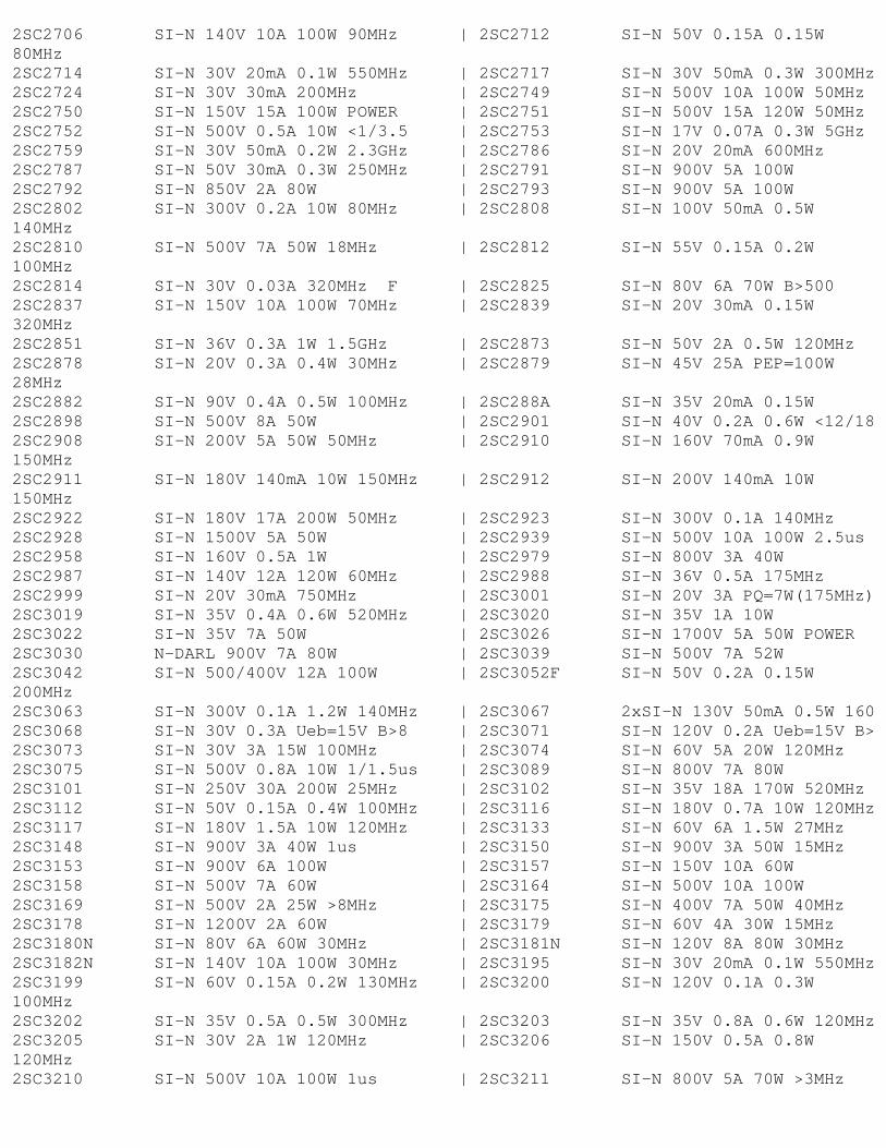
2SC2706 SI-N 140V 10A 100W 90MHz | 2SC2712 SI-N 50V 0.15A 0.15W80MHz 2SC2714 SI-N 30V 20mA 0.1W 550MHz | 2SC2717 SI-N 30V 50mA 0.3W 300MHz 2SC2724 SI-N 30V 30mA 200MHz | 2SC2749 SI-N 500V 10A 100W 50MHz 2SC2750 SI-N 150V 15A 100W POWER | 2SC2751 SI-N 500V 15A 120W 50MHz 2SC2752 SI-N 500V 0.5A 10W <1/3.5 | 2SC2753 SI-N 17V 0.07A 0.3W 5GHz 2SC2759 SI-N 30V 50mA 0.2W 2.3GHz | 2SC2786 SI-N 20V 20mA 600MHz 2SC2787 SI-N 50V 30mA 0.3W 250MHz | 2SC2791 SI-N 900V 5A 100W 2SC2792 SI-N 850V 2A 80W | 2SC2793 SI-N 900V 5A 100W 2SC2802 SI-N 300V 0.2A 10W 80MHz | 2SC2808 SI-N 100V 50mA 0.5W140MHz 2SC2810 SI-N 500V 7A 50W 18MHz | 2SC2812 SI-N 55V 0.15A 0.2W100MHz 2SC2814 SI-N 30V 0.03A 320MHz F | 2SC2825 SI-N 80V 6A 70W B>500 2SC2837 SI-N 150V 10A 100W 70MHz | 2SC2839 SI-N 20V 30mA 0.15W320MHz 2SC2851 SI-N 36V 0.3A 1W 1.5GHz | 2SC2873 SI-N 50V 2A 0.5W 120MHz 2SC2878 SI-N 20V 0.3A 0.4W 30MHz | 2SC2879 SI-N 45V 25A PEP=100W28MHz 2SC2882 SI-N 90V 0.4A 0.5W 100MHz | 2SC288A SI-N 35V 20mA 0.15W 2SC2898 SI-N 500V 8A 50W | 2SC2901 SI-N 40V 0.2A 0.6W <12/18 2SC2908 SI-N 200V 5A 50W 50MHz | 2SC2910 SI-N 160V 70mA 0.9W150MHz 2SC2911 SI-N 180V 140mA 10W 150MHz | 2SC2912 SI-N 200V 140mA 10W150MHz 2SC2922 SI-N 180V 17A 200W 50MHz | 2SC2923 SI-N 300V 0.1A 140MHz 2SC2928 SI-N 1500V 5A 50W | 2SC2939 SI-N 500V 10A 100W 2.5us 2SC2958 SI-N 160V 0.5A 1W | 2SC2979 SI-N 800V 3A 40W 2SC2987 SI-N 140V 12A 120W 60MHz | 2SC2988 SI-N 36V 0.5A 175MHz 2SC2999 SI-N 20V 30mA 750MHz | 2SC3001 SI-N 20V 3A PQ=7W(175MHz) 2SC3019 SI-N 35V 0.4A 0.6W 520MHz | 2SC3020 SI-N 35V 1A 10W 2SC3022 SI-N 35V 7A 50W | 2SC3026 SI-N 1700V 5A 50W POWER 2SC3030 N-DARL 900V 7A 80W | 2SC3039 SI-N 500V 7A 52W 2SC3042 SI-N 500/400V 12A 100W | 2SC3052F SI-N 50V 0.2A 0.15W200MHz 2SC3063 SI-N 300V 0.1A 1.2W 140MHz | 2SC3067 2xSI-N 130V 50mA 0.5W 160 2SC3068 SI-N 30V 0.3A Ueb=15V B>8 | 2SC3071 SI-N 120V 0.2A Ueb=15V B> 2SC3073 SI-N 30V 3A 15W 100MHz | 2SC3074 SI-N 60V 5A 20W 120MHz 2SC3075 SI-N 500V 0.8A 10W 1/1.5us | 2SC3089 SI-N 800V 7A 80W 2SC3101 SI-N 250V 30A 200W 25MHz | 2SC3102 SI-N 35V 18A 170W 520MHz 2SC3112 SI-N 50V 0.15A 0.4W 100MHz | 2SC3116 SI-N 180V 0.7A 10W 120MHz 2SC3117 SI-N 180V 1.5A 10W 120MHz | 2SC3133 SI-N 60V 6A 1.5W 27MHz 2SC3148 SI-N 900V 3A 40W 1us | 2SC3150 SI-N 900V 3A 50W 15MHz 2SC3153 SI-N 900V 6A 100W | 2SC3157 SI-N 150V 10A 60W 2SC3158 SI-N 500V 7A 60W | 2SC3164 SI-N 500V 10A 100W 2SC3169 SI-N 500V 2A 25W >8MHz | 2SC3175 SI-N 400V 7A 50W 40MHz 2SC3178 SI-N 1200V 2A 60W | 2SC3179 SI-N 60V 4A 30W 15MHz 2SC3180N SI-N 80V 6A 60W 30MHz | 2SC3181N SI-N 120V 8A 80W 30MHz 2SC3182N SI-N 140V 10A 100W 30MHz | 2SC3195 SI-N 30V 20mA 0.1W 550MHz 2SC3199 SI-N 60V 0.15A 0.2W 130MHz | 2SC3200 SI-N 120V 0.1A 0.3W100MHz 2SC3202 SI-N 35V 0.5A 0.5W 300MHz | 2SC3203 SI-N 35V 0.8A 0.6W 120MHz 2SC3205 SI-N 30V 2A 1W 120MHz | 2SC3206 SI-N 150V 0.5A 0.8W120MHz 2SC3210 SI-N 500V 10A 100W 1us | 2SC3211 SI-N 800V 5A 70W >3MHz
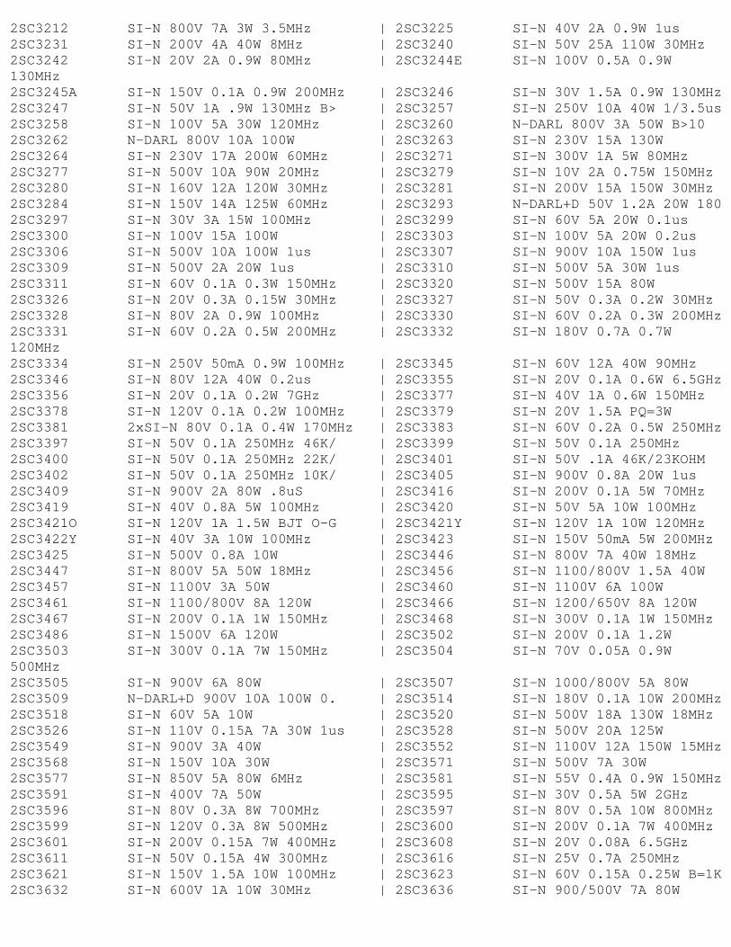
2SC3212 SI-N 800V 7A 3W 3.5MHz | 2SC3225 SI-N 40V 2A 0.9W 1us 2SC3231 SI-N 200V 4A 40W 8MHz | 2SC3240 SI-N 50V 25A 110W 30MHz 2SC3242 SI-N 20V 2A 0.9W 80MHz | 2SC3244E SI-N 100V 0.5A 0.9W130MHz 2SC3245A SI-N 150V 0.1A 0.9W 200MHz | 2SC3246 SI-N 30V 1.5A 0.9W 130MHz 2SC3247 SI-N 50V 1A .9W 130MHz B> | 2SC3257 SI-N 250V 10A 40W 1/3.5us 2SC3258 SI-N 100V 5A 30W 120MHz | 2SC3260 N-DARL 800V 3A 50W B>10 2SC3262 N-DARL 800V 10A 100W | 2SC3263 SI-N 230V 15A 130W 2SC3264 SI-N 230V 17A 200W 60MHz | 2SC3271 SI-N 300V 1A 5W 80MHz 2SC3277 SI-N 500V 10A 90W 20MHz | 2SC3279 SI-N 10V 2A 0.75W 150MHz 2SC3280 SI-N 160V 12A 120W 30MHz | 2SC3281 SI-N 200V 15A 150W 30MHz 2SC3284 SI-N 150V 14A 125W 60MHz | 2SC3293 N-DARL+D 50V 1.2A 20W 180 2SC3297 SI-N 30V 3A 15W 100MHz | 2SC3299 SI-N 60V 5A 20W 0.1us 2SC3300 SI-N 100V 15A 100W | 2SC3303 SI-N 100V 5A 20W 0.2us 2SC3306 SI-N 500V 10A 100W 1us | 2SC3307 SI-N 900V 10A 150W 1us 2SC3309 SI-N 500V 2A 20W 1us | 2SC3310 SI-N 500V 5A 30W 1us 2SC3311 SI-N 60V 0.1A 0.3W 150MHz | 2SC3320 SI-N 500V 15A 80W 2SC3326 SI-N 20V 0.3A 0.15W 30MHz | 2SC3327 SI-N 50V 0.3A 0.2W 30MHz 2SC3328 SI-N 80V 2A 0.9W 100MHz | 2SC3330 SI-N 60V 0.2A 0.3W 200MHz 2SC3331 SI-N 60V 0.2A 0.5W 200MHz | 2SC3332 SI-N 180V 0.7A 0.7W120MHz 2SC3334 SI-N 250V 50mA 0.9W 100MHz | 2SC3345 SI-N 60V 12A 40W 90MHz 2SC3346 SI-N 80V 12A 40W 0.2us | 2SC3355 SI-N 20V 0.1A 0.6W 6.5GHz 2SC3356 SI-N 20V 0.1A 0.2W 7GHz | 2SC3377 SI-N 40V 1A 0.6W 150MHz 2SC3378 SI-N 120V 0.1A 0.2W 100MHz | 2SC3379 SI-N 20V 1.5A PQ=3W 2SC3381 2xSI-N 80V 0.1A 0.4W 170MHz | 2SC3383 SI-N 60V 0.2A 0.5W 250MHz 2SC3397 SI-N 50V 0.1A 250MHz 46K/ | 2SC3399 SI-N 50V 0.1A 250MHz 2SC3400 SI-N 50V 0.1A 250MHz 22K/ | 2SC3401 SI-N 50V .1A 46K/23KOHM 2SC3402 SI-N 50V 0.1A 250MHz 10K/ | 2SC3405 SI-N 900V 0.8A 20W 1us 2SC3409 SI-N 900V 2A 80W .8uS | 2SC3416 SI-N 200V 0.1A 5W 70MHz 2SC3419 SI-N 40V 0.8A 5W 100MHz | 2SC3420 SI-N 50V 5A 10W 100MHz 2SC3421O SI-N 120V 1A 1.5W BJT O-G | 2SC3421Y SI-N 120V 1A 10W 120MHz 2SC3422Y SI-N 40V 3A 10W 100MHz | 2SC3423 SI-N 150V 50mA 5W 200MHz 2SC3425 SI-N 500V 0.8A 10W | 2SC3446 SI-N 800V 7A 40W 18MHz 2SC3447 SI-N 800V 5A 50W 18MHz | 2SC3456 SI-N 1100/800V 1.5A 40W 2SC3457 SI-N 1100V 3A 50W | 2SC3460 SI-N 1100V 6A 100W 2SC3461 SI-N 1100/800V 8A 120W | 2SC3466 SI-N 1200/650V 8A 120W 2SC3467 SI-N 200V 0.1A 1W 150MHz | 2SC3468 SI-N 300V 0.1A 1W 150MHz 2SC3486 SI-N 1500V 6A 120W | 2SC3502 SI-N 200V 0.1A 1.2W 2SC3503 SI-N 300V 0.1A 7W 150MHz | 2SC3504 SI-N 70V 0.05A 0.9W500MHz 2SC3505 SI-N 900V 6A 80W | 2SC3507 SI-N 1000/800V 5A 80W 2SC3509 N-DARL+D 900V 10A 100W 0. | 2SC3514 SI-N 180V 0.1A 10W 200MHz 2SC3518 SI-N 60V 5A 10W | 2SC3520 SI-N 500V 18A 130W 18MHz 2SC3526 SI-N 110V 0.15A 7A 30W 1us | 2SC3528 SI-N 500V 20A 125W 2SC3549 SI-N 900V 3A 40W | 2SC3552 SI-N 1100V 12A 150W 15MHz 2SC3568 SI-N 150V 10A 30W | 2SC3571 SI-N 500V 7A 30W 2SC3577 SI-N 850V 5A 80W 6MHz | 2SC3581 SI-N 55V 0.4A 0.9W 150MHz 2SC3591 SI-N 400V 7A 50W | 2SC3595 SI-N 30V 0.5A 5W 2GHz 2SC3596 SI-N 80V 0.3A 8W 700MHz | 2SC3597 SI-N 80V 0.5A 10W 800MHz 2SC3599 SI-N 120V 0.3A 8W 500MHz | 2SC3600 SI-N 200V 0.1A 7W 400MHz 2SC3601 SI-N 200V 0.15A 7W 400MHz | 2SC3608 SI-N 20V 0.08A 6.5GHz 2SC3611 SI-N 50V 0.15A 4W 300MHz | 2SC3616 SI-N 25V 0.7A 250MHz 2SC3621 SI-N 150V 1.5A 10W 100MHz | 2SC3623 SI-N 60V 0.15A 0.25W B=1K 2SC3632 SI-N 600V 1A 10W 30MHz | 2SC3636 SI-N 900/500V 7A 80W
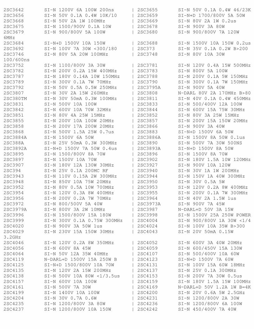
2SC3642 SI-N 1200V 6A 100W 200ns | 2SC3655 SI-N 50V 0.1A 0.4W 46/23K 2SC3656 SI-N 50V 0.1A 0.4W 10K/10 | 2SC3659 SI-N+D 1700/800V 5A 50W 2SC3668 SI-N 50V 2A 1W 100MHz | 2SC3669 SI-N 80V 2A 1W 0.2us 2SC3675 SI-N 1500/900V 0.1A 10W | 2SC3678 SI-N 900V 3A 80W 2SC3679 SI-N 900/800V 5A 100W | 2SC3680 SI-N 900/800V 7A 120W6MHz 2SC3684 SI-N+D 1500V 10A 150W | 2SC3688 SI-N 1500V 10A 150W 0.2us 2SC3692 SI-N 100V 7A 30W <300/180 | 2SC373 SI-N 35V 0.1A 0.2W B>200 2SC3746 SI-N 80V 5A 20W 100MHz | 2SC3748 SI-N 80V 10A 30W100/600ns 2SC3752 SI-N 1100/800V 3A 30W | 2SC3781 SI-N 120V 0.4A 15W 500MHz 2SC3782 SI-N 200V 0.2A 15W 400MHz | 2SC3783 SI-N 800V 5A 100W 2SC3787 SI-N 180V 0.14A 10W 150MHz | 2SC3788 SI-N 200V 0.1A 5W 150MHz 2SC3789 SI-N 300V 0.1A 7W 70MHz | 2SC3790 SI-N 300V 0.1A 7W 150MHz 2SC3792 SI-N 50V 0.5A 0.5W 250MHz | 2SC3795A SI-N 900V 5A 40W 2SC3807 SI-N 30V 2A 15W 260MHz | 2SC3808 N-DARL 80V 2A 170MHz B>80 2SC380TM SI-N 30V 50mA 0.3W 100MHz | 2SC3811 SI-N 40V 0.1A 0.4W 450MHz 2SC3831 SI-N 500V 10A 100W | 2SC3833 SI-N 500/400V 12A 100W 2SC3842 SI-N 600V 10A 70W 32MHz | 2SC3844 SI-N 600V 15A 75W 30MHz 2SC3851 SI-N 80V 4A 25W 15MHz | 2SC3852 SI-N 80V 3A 25W 15MHz 2SC3855 SI-N 200V 10A 100W 20MHz | 2SC3857 SI-N 200V 15A 150W 20MHz 2SC3858 SI-N 200V 17A 200W 20MHz | 2SC3866 SI-N 900V 3A 40W 2SC3868 SI-N 500V 1.5A 25W 0.7us | 2SC3883 SI-N+D 1500V 6A 50W 2SC3884A SI-N 1500V 6A 50W | 2SC3886A SI-N 1500V 8A 50W 0.1us 2SC388A SI-N 25V 50mA 0.3W 300MHz | 2SC3890 SI-N 500V 7A 30W 500NS 2SC3892A SI-N+D 1500V 7A 50W 0.4us | 2SC3893A SI-N+D 1500V 8A 50W 2SC3895 SI-N 1500/800V 8A 70W | 2SC3896 SI-N 1500V 8A 70W 2SC3897 SI-N 1500V 10A 70W | 2SC3902 SI-N 180V 1.5A 10W 120MHz 2SC3907 SI-N 180V 12A 130W 30MHz | 2SC3927 SI-N 900V 10A 120W 2SC394 SI-N 25V 0.1A 200MC RF | 2SC3940 SI-N 30V 1A 1W 200MHz 2SC3943 SI-N 110V 0.15A 2W 300MHz | 2SC3944 SI-N 150V 1A 40W 300MHz 2SC3948 SI-N 850V 10A 75W 20MHz | 2SC3950 SI-N 30V 0.5A 5W 2SC3952 SI-N 80V 0.5A 10W 700MHz | 2SC3953 SI-N 120V 0.2A 8W 400MHz 2SC3954 SI-N 120V 0.3A 8W 400MHz | 2SC3955 SI-N 200V 0.1A 7W 300MHz 2SC3956 SI-N 200V 0.2A 7W 70MHz | 2SC3964 SI-N 40V 2A 1.5W 1us 2SC3972 SI-N 800/500V 5A 40W | 2SC3973A SI-N 900V 7A 45W 2SC3979A SI-N 800V 3A 2W 10MHz | 2SC3987 N-DARL+D 50V 3A 15W 2SC3996 SI-N 1500/800V 15A 180W | 2SC3998 SI-N 1500V 25A 250W POWER 2SC3999 SI-N 300V 0.1A 0.75W 300MHz | 2SC4004 SI-N 900/800V 1A 30W <1/4 2SC4020 SI-N 900V 3A 50W 1us | 2SC4024 SI-N 100V 10A 35W B>300 2SC4029 SI-N 230V 15A 150W 30MHz | 2SC4043 SI-N 20V 50mA 0.15W3.2GHz 2SC4046 SI-N 120V 0.2A 8W 350MHz | 2SC4052 SI-N 600V 3A 40W 20MHz 2SC4056 SI-N 600V 8A 45W | 2SC4059 SI-N 600/450V 15A 130W 2SC4064 SI-N 50V 12A 35W 40MHz | 2SC4107 SI-N 500/400V 10A 60W 2SC4119 N-DARL+D 1500V 15A 250W B | 2SC4123 SI-N+D 1500V 7A 60W 2SC4125 SI-N+D 1500/800V 10A 70W | 2SC4131 SI-N 100V 15A 60W 18MHz 2SC4135 SI-N 120V 2A 15W 200MHz | 2SC4137 SI-N 25V 0.1A 300MHz 2SC4138 SI-N 500V 10A 80W <1/3.5us | 2SC4153 SI-N 200V 7A 30W 0.5us 2SC4157 SI-N 600V 10A 100W | 2SC4159 SI-N 180V 1.5A 15W 100MHz 2SC4161 SI-N 500V 7A 30W | 2SC4169 N-DARL+D 50V 1.2A 1W B=4K 2SC4199 SI-N 1400V 10A 100W | 2SC4200 SI-N 20V 0.6A 5W 2.5GHz 2SC4204 SI-N 30V 0.7A 0.6W | 2SC4231 SI-N 1200/800V 2A 30W 2SC4235 SI-N 1200/800V 3A 80W | 2SC4236 SI-N 1200/800V 6A 100W 2SC4237 SI-N 1200/800V 10A 150W | 2SC4242 SI-N 450/400V 7A 40W
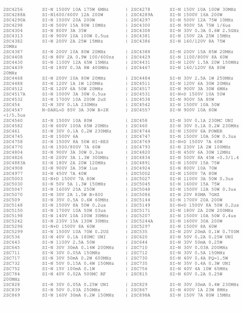
2SC4256 SI-N 1500V 10A 175W 6MHz | 2SC4278 SI-N 150V 10A 100W 30MHz 2SC4288A SI-N1600/600V 12A 200W | 2SC4289A SI-N 1500V 16A 200W 2SC4290A SI-N 1500V 20A 200W | 2SC4297 SI-N 500V 12A 75W 10MHz 2SC4298 SI-N 500V 15A 80W 10MHz | 2SC4300 SI-N 900V 5A 75W 1/6us 2SC4304 SI-N 800V 3A 35W | 2SC4308 SI-N 30V 0.3A 0.6W 2.5GHz 2SC4313 SI-N 900V 10A 100W 0.5us | 2SC4381 SI-N 150V 2A 25W 15MHz 2SC4382 SI-N 200V 2A 25W 15MHz | 2SC4386 SI-N 160/120V 8A 75W20MHz 2SC4387 SI-N 200V 10A 80W 20MHz | 2SC4388 SI-N 200V 15A 85W 20MHz 2SC4408 SI-N 80V 2A 0.9W 100/600ns | 2SC4429 SI-N 1100/800V 8A 60W 2SC4430 SI-N 1100V 12A 65W 15MHz | 2SC4431 SI-N 120V 1.5A 20W 150MHz 2SC4439 SI-N 180V 0.3A 8W 400MHz | 2SC4467 SI-N 160/120V 8A 80W20MHz 2SC4468 SI-N 200V 10A 80W 20MHz | 2SC4484 SI-N 30V 2.5A 1W 250MHz 2SC4488 SI-N 120V 1A 1W 120MHz | 2SC4511 SI-N 120V 6A 30W 20MHz 2SC4512 SI-N 120V 6A 50W 20MHz | 2SC4517 SI-N 900V 3A 30W 6MHz 2SC4517A SI-N 1000V 3A 30W 0.5us | 2SC4531 SI-N+D 1500V 10A 50W 2SC4532 SI-N 1700V 10A 200W 2uS | 2SC4538 SI-N 900V 5A 80W 2SC454 SI-N 30V 0.1A 230MHz | 2SC4542 SI-N 1500V 10A 50W 2SC4547 N-DARL+D 85V 3A 30W B>2K | 2SC4557 SI-N 900V 10A 80W<1/5.5us 2SC4560 SI-N 1500V 10A 80W | 2SC458 SI-N 30V 0.1A 230MC UNI 2SC4582 SI-N 600V 100A 65W 20MHz | 2SC460 SI-N 30V 0.1A 0.2W 230MHz 2SC461 SI-N 30V 0.1A 0.2W 230MHz | 2SC4744 SI-N 1500V 6A POWER 2SC4745 SI-N 1500V 6A | 2SC4747 SI-N 1500V 10A 50W 0.3us 2SC4758 SI-N 1500V 8A 50W HI-RES | 2SC4769 SI-N+D 1500V 7A 60W 2SC4770 SI-N 1500/800V 7A 60W | 2SC4793 SI-N 230V 1A 2W 100MHz 2SC4804 SI-N 900V 3A 30W 0.3us | 2SC4820 SI-N 450V 6A 30W 12MHz 2SC4826 SI-N 200V 3A 1.3W 300MHz | 2SC4834 SI-N 500V 8A 45W <0.3/1.4 2SC4883A SI-N 180V 2A 20W 120MHz | 2SC4891 SI-N 1500V 15A 75W 2SC4908 SI-N 900V 3A 35W 1us | 2SC4924 SI-N 800V 10A 70W 2SC4977 SI-N 450V 7A 40W | 2SC5002 SI-N 1500V 7A 80W 2SC5003 SI-N+D 1500V 7A 80W | 2SC5027 SI-N 1100V 3A 50W 0.3us 2SC5030 SI-N 50V 5A 1.3W 150MHz | 2SC5045 SI-N 1600V 15A 75W 2SC5047 SI-N 1600V 25A 250W | 2SC5048 SI-N 1500V 12A 50W 0.3us 2SC5070 SI-N 30V 2A 1.5W B>800 | 2SC5086 SI-N 20V 80MA 7GHZ 2SC509 SI-N 35V 0.5A 0.6W 60MHz | 2SC5144 SI-N 1700V 20A 200W 2SC5148 SI-N 1500V 8A 50W 0.2us | 2SC5149 SI-N+D 1500V 8A 50W 0.2us 2SC5150 SI-N 1700V 10A 50W 03us | 2SC5171 SI-N 180V 2A 20W 200MHz 2SC5198 SI-N 140V 10A 100W 30MHz | 2SC5207 SI-N 1500V 10A 50W 0.4us 2SC5242 SI-N 230V 15A 130W 30MHz | 2SC5244A SI-N 1600V 30A 200W 2SC5296 SI-N+D 1500V 8A 60W | 2SC5297 SI-N 1500V 8A 60W 2SC5299 SI-N 1500V 10A 70W 0.2US | 2SC535 SI-N 20V 20mA 0.1W 0.700M 2SC536 SI-N 40V 0.1A 180MC UNI | 2SC620 SI-N 50V 0.2A 0.25W UNI 2SC643 SI-N 1100V 2.5A 50W | 2SC644 SI-N 30V 50mA 0.25W 2SC645 SI-N 30V 30mA 0.14W 200MHz | 2SC710 SI-N 30V 0.03A 200MHz 2SC711 SI-N 30V 0.05A 150MHz | 2SC712 SI-N 30V 0.5A 150MHz 2SC717 SI-N 30V 50mA 0.2W 600MHz | 2SC730 SI-N 40V 0.4A PQ=1.5W 2SC732 SI-N 50V 0.15A 0.4W 150MHz | 2SC735 SI-N 35V 0.4A 0.3W UNI 2SC752 SI-N 15V 100mA 0.1W | 2SC756 SI-N 40V 4A 10W 65MHz 2SC784 SI-N 40V 0.02A 500MC RF | 2SC815 SI-N 60V 0.2A 0.25W200MHz 2SC828 SI-N 30V 0.05A 0.25W UNI | 2SC829 SI-N 30V 30mA 0.4W 230MHz 2SC839 SI-N 50V 0.03A 250MHz | 2SC867 SI-N 400V 1A 23W 8MHz 2SC869 SI-N 160V 30mA 0.2W 150MHz | 2SC898A SI-N 150V 7A 80W 15MHz
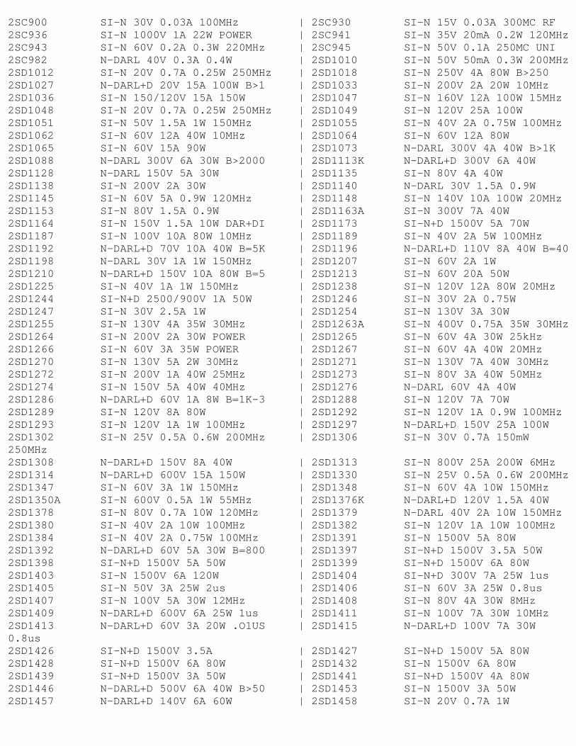
2SC900 SI-N 30V 0.03A 100MHz | 2SC930 SI-N 15V 0.03A 300MC RF 2SC936 SI-N 1000V 1A 22W POWER | 2SC941 SI-N 35V 20mA 0.2W 120MHz 2SC943 SI-N 60V 0.2A 0.3W 220MHz | 2SC945 SI-N 50V 0.1A 250MC UNI 2SC982 N-DARL 40V 0.3A 0.4W | 2SD1010 SI-N 50V 50mA 0.3W 200MHz 2SD1012 SI-N 20V 0.7A 0.25W 250MHz | 2SD1018 SI-N 250V 4A 80W B>250 2SD1027 N-DARL+D 20V 15A 100W B>1 | 2SD1033 SI-N 200V 2A 20W 10MHz 2SD1036 SI-N 150/120V 15A 150W | 2SD1047 SI-N 160V 12A 100W 15MHz 2SD1048 SI-N 20V 0.7A 0.25W 250MHz | 2SD1049 SI-N 120V 25A 100W 2SD1051 SI-N 50V 1.5A 1W 150MHz | 2SD1055 SI-N 40V 2A 0.75W 100MHz 2SD1062 SI-N 60V 12A 40W 10MHz | 2SD1064 SI-N 60V 12A 80W 2SD1065 SI-N 60V 15A 90W | 2SD1073 N-DARL 300V 4A 40W B>1K 2SD1088 N-DARL 300V 6A 30W B>2000 | 2SD1113K N-DARL+D 300V 6A 40W 2SD1128 N-DARL 150V 5A 30W | 2SD1135 SI-N 80V 4A 40W 2SD1138 SI-N 200V 2A 30W | 2SD1140 N-DARL 30V 1.5A 0.9W 2SD1145 SI-N 60V 5A 0.9W 120MHz | 2SD1148 SI-N 140V 10A 100W 20MHz 2SD1153 SI-N 80V 1.5A 0.9W | 2SD1163A SI-N 300V 7A 40W 2SD1164 SI-N 150V 1.5A 10W DAR+DI | 2SD1173 SI-N+D 1500V 5A 70W 2SD1187 SI-N 100V 10A 80W 10MHz | 2SD1189 SI-N 40V 2A 5W 100MHz 2SD1192 N-DARL+D 70V 10A 40W B=5K | 2SD1196 N-DARL+D 110V 8A 40W B=40 2SD1198 N-DARL 30V 1A 1W 150MHz | 2SD1207 SI-N 60V 2A 1W 2SD1210 N-DARL+D 150V 10A 80W B=5 | 2SD1213 SI-N 60V 20A 50W 2SD1225 SI-N 40V 1A 1W 150MHz | 2SD1238 SI-N 120V 12A 80W 20MHz 2SD1244 SI-N+D 2500/900V 1A 50W | 2SD1246 SI-N 30V 2A 0.75W 2SD1247 SI-N 30V 2.5A 1W | 2SD1254 SI-N 130V 3A 30W 2SD1255 SI-N 130V 4A 35W 30MHz | 2SD1263A SI-N 400V 0.75A 35W 30MHz 2SD1264 SI-N 200V 2A 30W POWER | 2SD1265 SI-N 60V 4A 30W 25kHz 2SD1266 SI-N 60V 3A 35W POWER | 2SD1267 SI-N 60V 4A 40W 20MHz 2SD1270 SI-N 130V 5A 2W 30MHz | 2SD1271 SI-N 130V 7A 40W 30MHz 2SD1272 SI-N 200V 1A 40W 25MHz | 2SD1273 SI-N 80V 3A 40W 50MHz 2SD1274 SI-N 150V 5A 40W 40MHz | 2SD1276 N-DARL 60V 4A 40W 2SD1286 N-DARL+D 60V 1A 8W B=1K-3 | 2SD1288 SI-N 120V 7A 70W 2SD1289 SI-N 120V 8A 80W | 2SD1292 SI-N 120V 1A 0.9W 100MHz 2SD1293 SI-N 120V 1A 1W 100MHz | 2SD1297 N-DARL+D 150V 25A 100W 2SD1302 SI-N 25V 0.5A 0.6W 200MHz | 2SD1306 SI-N 30V 0.7A 150mW250MHz 2SD1308 N-DARL+D 150V 8A 40W | 2SD1313 SI-N 800V 25A 200W 6MHz 2SD1314 N-DARL+D 600V 15A 150W | 2SD1330 SI-N 25V 0.5A 0.6W 200MHz 2SD1347 SI-N 60V 3A 1W 150MHz | 2SD1348 SI-N 60V 4A 10W 150MHz 2SD1350A SI-N 600V 0.5A 1W 55MHz | 2SD1376K N-DARL+D 120V 1.5A 40W 2SD1378 SI-N 80V 0.7A 10W 120MHz | 2SD1379 N-DARL 40V 2A 10W 150MHz 2SD1380 SI-N 40V 2A 10W 100MHz | 2SD1382 SI-N 120V 1A 10W 100MHz 2SD1384 SI-N 40V 2A 0.75W 100MHz | 2SD1391 SI-N 1500V 5A 80W 2SD1392 N-DARL+D 60V 5A 30W B=800 | 2SD1397 SI-N+D 1500V 3.5A 50W 2SD1398 SI-N+D 1500V 5A 50W | 2SD1399 SI-N+D 1500V 6A 80W 2SD1403 SI-N 1500V 6A 120W | 2SD1404 SI-N+D 300V 7A 25W 1us 2SD1405 SI-N 50V 3A 25W 2us | 2SD1406 SI-N 60V 3A 25W 0.8us 2SD1407 SI-N 100V 5A 30W 12MHz | 2SD1408 SI-N 80V 4A 30W 8MHz 2SD1409 N-DARL+D 600V 6A 25W 1us | 2SD1411 SI-N 100V 7A 30W 10MHz 2SD1413 N-DARL+D 60V 3A 20W .O1US | 2SD1415 N-DARL+D 100V 7A 30W0.8us 2SD1426 SI-N+D 1500V 3.5A | 2SD1427 SI-N+D 1500V 5A 80W 2SD1428 SI-N+D 1500V 6A 80W | 2SD1432 SI-N 1500V 6A 80W 2SD1439 SI-N+D 1500V 3A 50W | 2SD1441 SI-N+D 1500V 4A 80W 2SD1446 N-DARL+D 500V 6A 40W B>50 | 2SD1453 SI-N 1500V 3A 50W 2SD1457 N-DARL+D 140V 6A 60W | 2SD1458 SI-N 20V 0.7A 1W
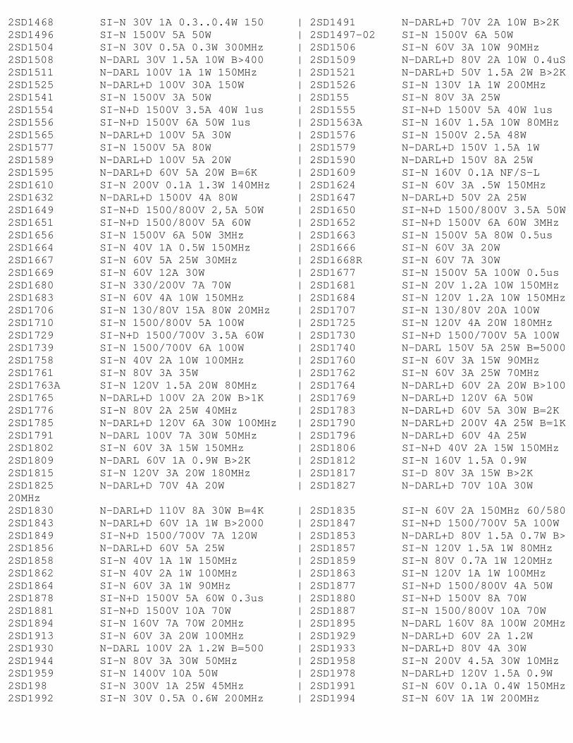
2SD1468 SI-N 30V 1A 0.3..0.4W 150 | 2SD1491 N-DARL+D 70V 2A 10W B>2K 2SD1496 SI-N 1500V 5A 50W | 2SD1497-02 SI-N 1500V 6A 50W 2SD1504 SI-N 30V 0.5A 0.3W 300MHz | 2SD1506 SI-N 60V 3A 10W 90MHz 2SD1508 N-DARL 30V 1.5A 10W B>400 | 2SD1509 N-DARL+D 80V 2A 10W 0.4uS 2SD1511 N-DARL 100V 1A 1W 150MHz | 2SD1521 N-DARL+D 50V 1.5A 2W B>2K 2SD1525 N-DARL+D 100V 30A 150W | 2SD1526 SI-N 130V 1A 1W 200MHz 2SD1541 SI-N 1500V 3A 50W | 2SD155 SI-N 80V 3A 25W 2SD1554 SI-N+D 1500V 3.5A 40W 1us | 2SD1555 SI-N+D 1500V 5A 40W 1us 2SD1556 SI-N+D 1500V 6A 50W 1us | 2SD1563A SI-N 160V 1.5A 10W 80MHz 2SD1565 N-DARL+D 100V 5A 30W | 2SD1576 SI-N 1500V 2.5A 48W 2SD1577 SI-N 1500V 5A 80W | 2SD1579 N-DARL+D 150V 1.5A 1W 2SD1589 N-DARL+D 100V 5A 20W | 2SD1590 N-DARL+D 150V 8A 25W 2SD1595 N-DARL+D 60V 5A 20W B=6K | 2SD1609 SI-N 160V 0.1A NF/S-L 2SD1610 SI-N 200V 0.1A 1.3W 140MHz | 2SD1624 SI-N 60V 3A .5W 150MHz 2SD1632 N-DARL+D 1500V 4A 80W | 2SD1647 N-DARL+D 50V 2A 25W 2SD1649 SI-N+D 1500/800V 2,5A 50W | 2SD1650 SI-N+D 1500/800V 3.5A 50W 2SD1651 SI-N+D 1500/800V 5A 60W | 2SD1652 SI-N+D 1500V 6A 60W 3MHz 2SD1656 SI-N 1500V 6A 50W 3MHz | 2SD1663 SI-N 1500V 5A 80W 0.5us 2SD1664 SI-N 40V 1A 0.5W 150MHz | 2SD1666 SI-N 60V 3A 20W 2SD1667 SI-N 60V 5A 25W 30MHz | 2SD1668R SI-N 60V 7A 30W 2SD1669 SI-N 60V 12A 30W | 2SD1677 SI-N 1500V 5A 100W 0.5us 2SD1680 SI-N 330/200V 7A 70W | 2SD1681 SI-N 20V 1.2A 10W 150MHz 2SD1683 SI-N 60V 4A 10W 150MHz | 2SD1684 SI-N 120V 1.2A 10W 150MHz 2SD1706 SI-N 130/80V 15A 80W 20MHz | 2SD1707 SI-N 130/80V 20A 100W 2SD1710 SI-N 1500/800V 5A 100W | 2SD1725 SI-N 120V 4A 20W 180MHz 2SD1729 SI-N+D 1500/700V 3.5A 60W | 2SD1730 SI-N+D 1500/700V 5A 100W 2SD1739 SI-N 1500/700V 6A 100W | 2SD1740 N-DARL 150V 5A 25W B=5000 2SD1758 SI-N 40V 2A 10W 100MHz | 2SD1760 SI-N 60V 3A 15W 90MHz 2SD1761 SI-N 80V 3A 35W | 2SD1762 SI-N 60V 3A 25W 70MHz 2SD1763A SI-N 120V 1.5A 20W 80MHz | 2SD1764 N-DARL+D 60V 2A 20W B>100 2SD1765 N-DARL+D 100V 2A 20W B>1K | 2SD1769 N-DARL+D 120V 6A 50W 2SD1776 SI-N 80V 2A 25W 40MHz | 2SD1783 N-DARL+D 60V 5A 30W B=2K 2SD1785 N-DARL+D 120V 6A 30W 100MHz | 2SD1790 N-DARL+D 200V 4A 25W B=1K 2SD1791 N-DARL 100V 7A 30W 50MHz | 2SD1796 N-DARL+D 60V 4A 25W 2SD1802 SI-N 60V 3A 15W 150MHz | 2SD1806 SI-N+D 40V 2A 15W 150MHz 2SD1809 N-DARL 60V 1A 0.9W B>2K | 2SD1812 SI-N 160V 1.5A 0.9W 2SD1815 SI-N 120V 3A 20W 180MHz | 2SD1817 SI-D 80V 3A 15W B>2K 2SD1825 N-DARL+D 70V 4A 20W | 2SD1827 N-DARL+D 70V 10A 30W20MHz 2SD1830 N-DARL+D 110V 8A 30W B=4K | 2SD1835 SI-N 60V 2A 150MHz 60/580 2SD1843 N-DARL+D 60V 1A 1W B>2000 | 2SD1847 SI-N+D 1500/700V 5A 100W 2SD1849 SI-N+D 1500/700V 7A 120W | 2SD1853 N-DARL+D 80V 1.5A 0.7W B> 2SD1856 N-DARL+D 60V 5A 25W | 2SD1857 SI-N 120V 1.5A 1W 80MHz 2SD1858 SI-N 40V 1A 1W 150MHz | 2SD1859 SI-N 80V 0.7A 1W 120MHz 2SD1862 SI-N 40V 2A 1W 100MHz | 2SD1863 SI-N 120V 1A 1W 100MHz 2SD1864 SI-N 60V 3A 1W 90MHz | 2SD1877 SI-N+D 1500/800V 4A 50W 2SD1878 SI-N+D 1500V 5A 60W 0.3us | 2SD1880 SI-N+D 1500V 8A 70W 2SD1881 SI-N+D 1500V 10A 70W | 2SD1887 SI-N 1500/800V 10A 70W 2SD1894 SI-N 160V 7A 70W 20MHz | 2SD1895 N-DARL 160V 8A 100W 20MHz 2SD1913 SI-N 60V 3A 20W 100MHz | 2SD1929 N-DARL+D 60V 2A 1.2W 2SD1930 N-DARL 100V 2A 1.2W B=500 | 2SD1933 N-DARL+D 80V 4A 30W 2SD1944 SI-N 80V 3A 30W 50MHz | 2SD1958 SI-N 200V 4.5A 30W 10MHz 2SD1959 SI-N 1400V 10A 50W | 2SD1978 N-DARL+D 120V 1.5A 0.9W 2SD198 SI-N 300V 1A 25W 45MHz | 2SD1991 SI-N 60V 0.1A 0.4W 150MHz 2SD1992 SI-N 30V 0.5A 0.6W 200MHz | 2SD1994 SI-N 60V 1A 1W 200MHz
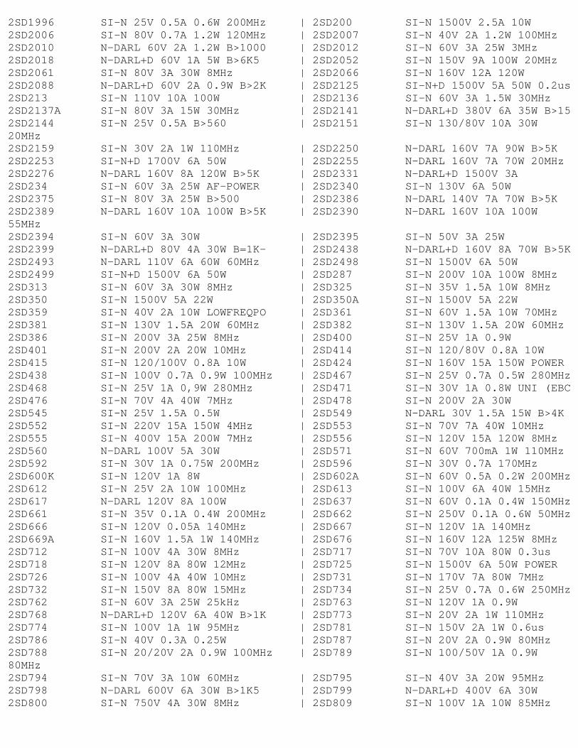
2SD1996 SI-N 25V 0.5A 0.6W 200MHz | 2SD200 SI-N 1500V 2.5A 10W 2SD2006 SI-N 80V 0.7A 1.2W 120MHz | 2SD2007 SI-N 40V 2A 1.2W 100MHz 2SD2010 N-DARL 60V 2A 1.2W B>1000 | 2SD2012 SI-N 60V 3A 25W 3MHz 2SD2018 N-DARL+D 60V 1A 5W B>6K5 | 2SD2052 SI-N 150V 9A 100W 20MHz 2SD2061 SI-N 80V 3A 30W 8MHz | 2SD2066 SI-N 160V 12A 120W 2SD2088 N-DARL+D 60V 2A 0.9W B>2K | 2SD2125 SI-N+D 1500V 5A 50W 0.2us 2SD213 SI-N 110V 10A 100W | 2SD2136 SI-N 60V 3A 1.5W 30MHz 2SD2137A SI-N 80V 3A 15W 30MHz | 2SD2141 N-DARL+D 380V 6A 35W B>15 2SD2144 SI-N 25V 0.5A B>560 | 2SD2151 SI-N 130/80V 10A 30W20MHz 2SD2159 SI-N 30V 2A 1W 110MHz | 2SD2250 N-DARL 160V 7A 90W B>5K 2SD2253 SI-N+D 1700V 6A 50W | 2SD2255 N-DARL 160V 7A 70W 20MHz 2SD2276 N-DARL 160V 8A 120W B>5K | 2SD2331 N-DARL+D 1500V 3A 2SD234 SI-N 60V 3A 25W AF-POWER | 2SD2340 SI-N 130V 6A 50W 2SD2375 SI-N 80V 3A 25W B>500 | 2SD2386 N-DARL 140V 7A 70W B>5K 2SD2389 N-DARL 160V 10A 100W B>5K | 2SD2390 N-DARL 160V 10A 100W55MHz 2SD2394 SI-N 60V 3A 30W | 2SD2395 SI-N 50V 3A 25W 2SD2399 N-DARL+D 80V 4A 30W B=1K- | 2SD2438 N-DARL+D 160V 8A 70W B>5K 2SD2493 N-DARL 110V 6A 60W 60MHz | 2SD2498 SI-N 1500V 6A 50W 2SD2499 SI-N+D 1500V 6A 50W | 2SD287 SI-N 200V 10A 100W 8MHz 2SD313 SI-N 60V 3A 30W 8MHz | 2SD325 SI-N 35V 1.5A 10W 8MHz 2SD350 SI-N 1500V 5A 22W | 2SD350A SI-N 1500V 5A 22W 2SD359 SI-N 40V 2A 10W LOWFREQPO | 2SD361 SI-N 60V 1.5A 10W 70MHz 2SD381 SI-N 130V 1.5A 20W 60MHz | 2SD382 SI-N 130V 1.5A 20W 60MHz 2SD386 SI-N 200V 3A 25W 8MHz | 2SD400 SI-N 25V 1A 0.9W 2SD401 SI-N 200V 2A 20W 10MHz | 2SD414 SI-N 120/80V 0.8A 10W 2SD415 SI-N 120/100V 0.8A 10W | 2SD424 SI-N 160V 15A 150W POWER 2SD438 SI-N 100V 0.7A 0.9W 100MHz | 2SD467 SI-N 25V 0.7A 0.5W 280MHz 2SD468 SI-N 25V 1A 0,9W 280MHz | 2SD471 SI-N 30V 1A 0.8W UNI (EBC 2SD476 SI-N 70V 4A 40W 7MHz | 2SD478 SI-N 200V 2A 30W 2SD545 SI-N 25V 1.5A 0.5W | 2SD549 N-DARL 30V 1.5A 15W B>4K 2SD552 SI-N 220V 15A 150W 4MHz | 2SD553 SI-N 70V 7A 40W 10MHz 2SD555 SI-N 400V 15A 200W 7MHz | 2SD556 SI-N 120V 15A 120W 8MHz 2SD560 N-DARL 100V 5A 30W | 2SD571 SI-N 60V 700mA 1W 110MHz 2SD592 SI-N 30V 1A 0.75W 200MHz | 2SD596 SI-N 30V 0.7A 170MHz 2SD600K SI-N 120V 1A 8W | 2SD602A SI-N 60V 0.5A 0.2W 200MHz 2SD612 SI-N 25V 2A 10W 100MHz | 2SD613 SI-N 100V 6A 40W 15MHz 2SD617 N-DARL 120V 8A 100W | 2SD637 SI-N 60V 0.1A 0.4W 150MHz 2SD661 SI-N 35V 0.1A 0.4W 200MHz | 2SD662 SI-N 250V 0.1A 0.6W 50MHz 2SD666 SI-N 120V 0.05A 140MHz | 2SD667 SI-N 120V 1A 140MHz 2SD669A SI-N 160V 1.5A 1W 140MHz | 2SD676 SI-N 160V 12A 125W 8MHz 2SD712 SI-N 100V 4A 30W 8MHz | 2SD717 SI-N 70V 10A 80W 0.3us 2SD718 SI-N 120V 8A 80W 12MHz | 2SD725 SI-N 1500V 6A 50W POWER 2SD726 SI-N 100V 4A 40W 10MHz | 2SD731 SI-N 170V 7A 80W 7MHz 2SD732 SI-N 150V 8A 80W 15MHz | 2SD734 SI-N 25V 0.7A 0.6W 250MHz 2SD762 SI-N 60V 3A 25W 25kHz | 2SD763 SI-N 120V 1A 0.9W 2SD768 N-DARL+D 120V 6A 40W B>1K | 2SD773 SI-N 20V 2A 1W 110MHz 2SD774 SI-N 100V 1A 1W 95MHz | 2SD781 SI-N 150V 2A 1W 0.6us 2SD786 SI-N 40V 0.3A 0.25W | 2SD787 SI-N 20V 2A 0.9W 80MHz 2SD788 SI-N 20/20V 2A 0.9W 100MHz | 2SD789 SI-N 100/50V 1A 0.9W80MHz 2SD794 SI-N 70V 3A 10W 60MHz | 2SD795 SI-N 40V 3A 20W 95MHz 2SD798 N-DARL 600V 6A 30W B>1K5 | 2SD799 N-DARL+D 400V 6A 30W 2SD800 SI-N 750V 4A 30W 8MHz | 2SD809 SI-N 100V 1A 10W 85MHz
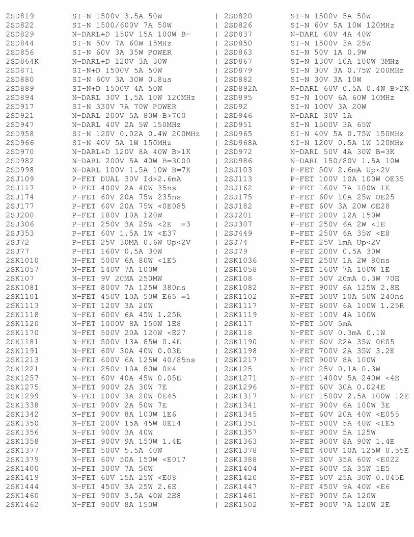
2SD819 SI-N 1500V 3.5A 50W | 2SD820 SI-N 1500V 5A 50W 2SD822 SI-N 1500/600V 7A 50W | 2SD826 SI-N 60V 5A 10W 120MHz 2SD829 N-DARL+D 150V 15A 100W B= | 2SD837 N-DARL 60V 4A 40W 2SD844 SI-N 50V 7A 60W 15MHz | 2SD850 SI-N 1500V 3A 25W 2SD856 SI-N 60V 3A 35W POWER | 2SD863 SI-N 50V 1A 0.9W 2SD864K N-DARL+D 120V 3A 30W | 2SD867 SI-N 130V 10A 100W 3MHz 2SD871 SI-N+D 1500V 5A 50W | 2SD879 SI-N 30V 3A 0.75W 200MHz 2SD880 SI-N 60V 3A 30W 0.8us | 2SD882 SI-N 30V 3A 10W 2SD889 SI-N+D 1500V 4A 50W | 2SD892A N-DARL 60V 0.5A 0.4W B>2K 2SD894 N-DARL 30V 1.5A 10W 120MHz | 2SD895 SI-N 100V 6A 60W 10MHz 2SD917 SI-N 330V 7A 70W POWER | 2SD92 SI-N 100V 3A 20W 2SD921 N-DARL 200V 5A 80W B>700 | 2SD946 N-DARL 30V 1A 2SD947 N-DARL 40V 2A 5W 150MHz | 2SD951 SI-N 1500V 3A 65W 2SD958 SI-N 120V 0.02A 0.4W 200MHz | 2SD965 SI-N 40V 5A 0.75W 150MHz 2SD966 SI-N 40V 5A 1W 150MHz | 2SD968A SI-N 120V 0.5A 1W 120MHz 2SD970 N-DARL+D 120V 8A 40W B>1K | 2SD972 N-DARL 50V 4A 30W B=3K 2SD982 N-DARL 200V 5A 40W B=3000 | 2SD986 N-DARL 150/80V 1.5A 10W 2SD998 N-DARL 100V 1.5A 10W B=7K | 2SJ103 P-FET 50V 2.6mA Up<2V 2SJ109 P-FET DUAL 30V Id>2.6mA | 2SJ113 P-FET 100V 10A 100W OE35 2SJ117 P-FET 400V 2A 40W 35ns | 2SJ162 P-FET 160V 7A 100W 1E 2SJ174 P-FET 60V 20A 75W 235ns | 2SJ175 P-FET 60V 10A 25W OE25 2SJ177 P-FET 60V 20A 75W <0E085 | 2SJ182 P-FET 60V 3A 20W OE28 2SJ200 P-FET 180V 10A 120W | 2SJ201 P-FET 200V 12A 150W 2SJ306 P-FET 250V 3A 25W <2E =3 | 2SJ307 P-FET 250V 6A 2W <1E 2SJ353 P-FET 60V 1.5A 1W <E37 | 2SJ449 P-FET 250V 6A 35W <E8 2SJ72 P-FET 25V 30MA 0.6W Up<2V | 2SJ74 P-FET 25V 1mA Up<2V 2SJ77 P-FET 160V 0.5A 30W | 2SJ79 P-FET 200V 0.5A 30W 2SK1010 N-FET 500V 6A 80W <1E5 | 2SK1036 N-FET 250V 1A 2W 80ns 2SK1057 N-FET 140V 7A 100W | 2SK1058 N-FET 160V 7A 100W 1E 2SK107 N-FET 9V 20MA 250MW | 2SK108 N-FET 50V 20mA 0.3W 70E 2SK1081 N-FET 800V 7A 125W 380ns | 2SK1082 N-FET 900V 6A 125W 2.8E 2SK1101 N-FET 450V 10A 50W E65 =1 | 2SK1102 N-FET 500V 10A 50W 240ns 2SK1113 N-FET 120V 3A 20W | 2SK1117 N-FET 600V 6A 100W 1.25R 2SK1118 N-FET 600V 6A 45W 1.25R | 2SK1119 N-FET 100V 4A 100W 2SK1120 N-FET 1000V 8A 150W 1E8 | 2SK117 N-FET 50V 5mA 2SK1170 N-FET 500V 20A 120W <E27 | 2SK118 N-FET 50V 0.3mA 0.1W 2SK1181 N-FET 500V 13A 85W 0.4E | 2SK1190 N-FET 60V 22A 35W 0E05 2SK1191 N-FET 60V 30A 40W 0.03E | 2SK1198 N-FET 700V 2A 35W 3.2E 2SK1213 N-FET 600V 6A 125W 40/85ns | 2SK1217 N-FET 900V 8A 100W 2SK1221 N-FET 250V 10A 80W 0E4 | 2SK125 N-FET 25V 0.1A 0.3W 2SK1257 N-FET 60V 40A 45W 0.05E | 2SK1271 N-FET 1400V 5A 240W <4E 2SK1275 N-FET 900V 2A 30W 7E | 2SK1296 N-FET 60V 30A 0.024E 2SK1299 N-FET 100V 3A 20W 0E45 | 2SK1317 N-FET 1500V 2.5A 100W 12E 2SK1338 N-FET 900V 2A 50W 7E | 2SK1341 N-FET 900V 6A 100W 3E 2SK1342 N-FET 900V 8A 100W 1E6 | 2SK1345 N-FET 60V 20A 40W <E055 2SK1350 N-FET 200V 15A 45W 0E14 | 2SK1351 N-FET 500V 5A 40W <1E5 2SK1356 N-FET 900V 3A 40W | 2SK1357 N-FET 900V 5A 125W 2SK1358 N-FET 900V 9A 150W 1.4E | 2SK1363 N-FET 900V 8A 90W 1.4E 2SK1377 N-FET 500V 5.5A 40W | 2SK1378 N-FET 400V 10A 125W 0.55E 2SK1379 N-FET 60V 50A 150W <E017 | 2SK1388 N-FET 30V 35A 60W <E022 2SK1400 N-FET 300V 7A 50W | 2SK1404 N-FET 600V 5A 35W 1E5 2SK1419 N-FET 60V 15A 25W <E08 | 2SK1420 N-FET 60V 25A 30W 0.045E 2SK1444 N-FET 450V 3A 25W 2.6E | 2SK1447 N-FET 450V 9A 40W <E6 2SK1460 N-FET 900V 3.5A 40W 2E8 | 2SK1461 N-FET 900V 5A 120W 2SK1462 N-FET 900V 8A 150W | 2SK1502 N-FET 900V 7A 120W 2E
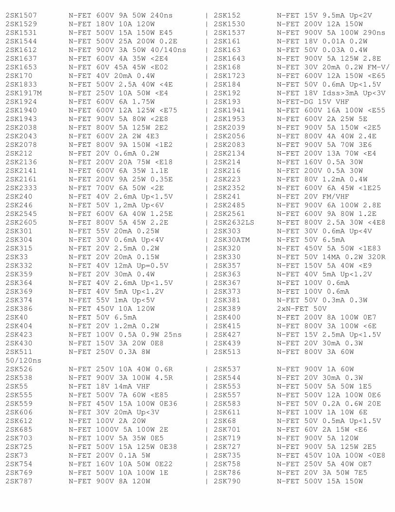
2SK1507 N-FET 600V 9A 50W 240ns | 2SK152 N-FET 15V 9.5mA Up<2V 2SK1529 N-FET 180V 10A 120W | 2SK1530 N-FET 200V 12A 150W 2SK1531 N-FET 500V 15A 150W E45 | 2SK1537 N-FET 900V 5A 100W 290ns 2SK1544 N-FET 500V 25A 200W 0.2E | 2SK161 N-FET 18V 0.01A 0.2W 2SK1612 N-FET 900V 3A 50W 40/140ns | 2SK163 N-FET 50V 0.03A 0.4W 2SK1637 N-FET 600V 4A 35W <2E4 | 2SK1643 N-FET 900V 5A 125W 2.8E 2SK1653 N-FET 60V 45A 45W <E02 | 2SK168 N-FET 30V 20mA 0.2W FM-V/ 2SK170 N-FET 40V 20mA 0.4W | 2SK1723 N-FET 600V 12A 150W <E65 2SK1833 N-FET 500V 2.5A 40W <4E | 2SK184 N-FET 50V 0.6mA Up<1.5V 2SK1917M N-FET 250V 10A 50W <E4 | 2SK192 N-FET 18V Idss>3mA Up<3V 2SK1924 N-FET 600V 6A 1.75W | 2SK193 N-FET-DG 15V VHF 2SK1940 N-FET 600V 12A 125W <E75 | 2SK1941 N-FET 600V 16A 100W <E55 2SK1943 N-FET 900V 5A 80W <2E8 | 2SK1953 N-FET 600V 2A 25W 5E 2SK2038 N-FET 800V 5A 125W 2E2 | 2SK2039 N-FET 900V 5A 150W <2E5 2SK2043 N-FET 600V 2A 2W 4E3 | 2SK2056 N-FET 800V 4A 40W 2.4E 2SK2078 N-FET 800V 9A 150W <1E2 | 2SK2083 N-FET 900V 5A 70W 3E6 2SK212 N-FET 20V 0.6mA 0.2W | 2SK2134 N-FET 200V 13A 70W <E4 2SK2136 N-FET 200V 20A 75W <E18 | 2SK214 N-FET 160V 0.5A 30W 2SK2141 N-FET 600V 6A 35W 1.1E | 2SK216 N-FET 200V 0.5A 30W 2SK2161 N-FET 200V 9A 25W 0.35E | 2SK223 N-FET 80V 1.2mA 0.4W 2SK2333 N-FET 700V 6A 50W <2E | 2SK2352 N-FET 600V 6A 45W <1E25 2SK240 N-FET 40V 2.6mA Up<1.5V | 2SK241 N-FET 20V FM/VHF 2SK246 N-FET 50V 1,2mA Up<6V | 2SK2485 N-FET 900V 6A 100W 2.8E 2SK2545 N-FET 600V 6A 40W 1.25E | 2SK2561 N-FET 600V 9A 80W 1.2E 2SK2605 N-FET 800V 5A 45W 2.2E | 2SK2632LS N-FET 800V 2.5A 30W <4E8 2SK301 N-FET 55V 20mA 0.25W | 2SK303 N-FET 30V 0.6mA Up<4V 2SK304 N-FET 30V 0.6mA Up<4V | 2SK30ATM N-FET 50V 6.5mA 2SK315 N-FET 20V 2.5mA 0.2W | 2SK320 N-FET 450V 5A 50W <1E83 2SK33 N-FET 20V 20mA 0.15W | 2SK330 N-FET 50V 14MA 0.2W 320R 2SK332 N-FET 40V 12mA Up=0.5V | 2SK357 N-FET 150V 5A 40W <E9 2SK359 N-FET 20V 30mA 0.4W | 2SK363 N-FET 40V 5mA Up<1.2V 2SK364 N-FET 40V 2.6mA Up<1.5V | 2SK367 N-FET 100V 0.6mA 2SK369 N-FET 40V 5mA Up<1.2V | 2SK373 N-FET 100V 0.6mA 2SK374 N-FET 55V 1mA Up<5V | 2SK381 N-FET 50V 0.3mA 0.3W 2SK386 N-FET 450V 10A 120W | 2SK389 2xN-FET 50V 2SK40 N-FET 50V 6.5mA | 2SK400 N-FET 200V 8A 100W 0E7 2SK404 N-FET 20V 1.2mA 0.2W | 2SK415 N-FET 800V 3A 100W <6E 2SK423 N-FET 100V 0.5A 0.9W 25ns | 2SK427 N-FET 15V 2.5mA Up<1.5V 2SK430 N-FET 150V 3A 20W 0E8 | 2SK439 N-FET 20V 30mA 0.3W 2SK511 N-FET 250V 0.3A 8W | 2SK513 N-FET 800V 3A 60W50/120ns 2SK526 N-FET 250V 10A 40W 0.6R | 2SK537 N-FET 900V 1A 60W 2SK538 N-FET 900V 3A 100W 4.5R | 2SK544 N-FET 20V 30mA 0.3W 2SK55 N-FET 18V 14mA VHF | 2SK553 N-FET 500V 5A 50W 1E5 2SK555 N-FET 500V 7A 60W <E85 | 2SK557 N-FET 500V 12A 100W 0E6 2SK559 N-FET 450V 15A 100W 0E36 | 2SK583 N-FET 50V 0.2A 0.6W 20E 2SK606 N-FET 30V 20mA Up<3V | 2SK611 N-FET 100V 1A 10W 6E 2SK612 N-FET 100V 2A 20W | 2SK68 N-FET 50V 0.5mA Up<1.5V 2SK685 N-FET 1000V 5A 100W 2E | 2SK701 N-FET 60V 2A 15W <E6 2SK703 N-FET 100V 5A 35W 0E5 | 2SK719 N-FET 900V 5A 120W 2SK725 N-FET 500V 15A 125W 0E38 | 2SK727 N-FET 900V 5A 125W 2E5 2SK73 N-FET 200V 0.1A 5W | 2SK735 N-FET 450V 10A 100W <0E8 2SK754 N-FET 160V 10A 50W 0E22 | 2SK758 N-FET 250V 5A 40W OE7 2SK769 N-FET 500V 10A 100W 1E | 2SK786 N-FET 20V 3A 50W 7E5 2SK787 N-FET 900V 8A 120W | 2SK790 N-FET 500V 15A 150W

2SK791 N-FET 850V 3A 100W 4.5R | 2SK792 N-FET 900V 3A 100W 4.5R 2SK793 N-FET 850V 5A 150W 2.5R | 2SK794 N-FET 900V 5A 150W 2.5R 2SK796 N-FET 800V 3A 90W 5E | 2SK806 N-FET 600V 3A 50W <2E7 2SK817 N-FET 60V 26A 35W 0.08E | 2SK83 N-FET 25V 10MA 0.1W Up<2. 2SK851 N-FET 200V 30A 150W | 2SK856 N-FET 60V 45A 125W <E03 2SK872 N-FET 900V 6A 150W 2.5E | 2SK875 N-FET 450V 12A 120W 0.6E 2SK890 N-FET 200V 10A 75W <E4 | 2SK891 N-FET 100V 18A 125W <E18 2SK899 N-FET 500V 18A 125W <E33 | 2SK902 N-FET 250V 30A 150W 2SK903 N-FET 800V 3A 40W 4E | 2SK904 N-FET 800V 3A 80W 4E 2SK940 N-FET 60V 0.8A 0.9W 1.1E | 2SK943 N-FET 60V 25A 40W E046 2SK951 N-FET 800V 2.5A 40W 7E | 2SK952 N-FET 800V 0.5mA 2SK955 N-FET 800V 5A 125W 2E | 2SK956 N-FET 800V 9A 150W 1E5 2SK962 N-FET 900V 0.5mA Up>2.5V | 3SK131 N-FET-DG 20V 25mA 0.2W 3SK60 N-FET-DG 15V 33mA | 3SK73 N-FET-DG 20V 3mA 3SK74 N-FET-DG 20V 25mA 0.2W | AC121 GE-P 20V 0.3A 0.9W AC122 GE-P 30V 0.2A 0.225W | AC125 GE-P 32V 0.2A AC126 GE-P 32V 0.2A 0.5W | AC127 GE-N 32V 0.5A AC128 GE-P 32V 1A 1W | AC128/176K GE N/P PAIRED, COOLED AC128K GE-P 32V 1A 1W | AC131 GE-P 30V 1A 0.75W AC132 GE-P 32V 0.2A 0.5W | AC138 GE-P 32V 1.2A 0.22W1.5MHz AC141K GE-N 32V 1.2A 1W | AC151 GE-P 32V 0.2A 0.9W AC153 GE-P 32V 2A 1W | AC153K GE-P 32V 2A 1W AC176K GE-N 32V 1A 1W | AC180 GE-P 32V 1.5A 0.3W 1MHz AC187 GE-N 25V 1A 1W | AC187/188K GE N/P PAIRED,COOLED AC187K GE-N 25V 1A 1W COOLED | AC188 GE-P 25V 1A 1W AC188K GE-P 25V 1A 1W | AD133 GE-P 50V 15A 36W AD136 GE-P 40V 10A 11W | AD139 GE-P 32V 3.5A 13W AD148 GE-P 32V 3.5A 13.5W | AD149 GE-P 50V 3.5A 27W AD161 GE-N 32V 1A 6W | AD161/162 GE N/P 32V 1A 6W PAIRED AD162 GE-P 32V 1A 6W | AD165 GE-N 25V 1A 6W AD166 GE-P 60V 5A 27.5W | AF106 GE-P 25V 10mA 220MHz VHF AF109R GE-P 20V 12mA 260MHz VHF | AF118 GE-P 70V 30mA 375mW125MHz AF121 GE-P 25V 10mA 270MHz | AF125 GE-P 32V 10mA 75MHz AF127 GE-P 32V 10mA 75MHz | AF139 GE-P 20V 10mA 550MHz AF200 GE-P 25V 10mA 0.145W | AF201 GE-P 25V 10mA 0.145W AF239S GE-P 15V 10mA 700MHz | AF279 GE-P 15V 10mA 60mW 780MHz AF279S GE-P 20V 10mA 0.6W | AF280 GE-P UHF MIXER 550MHz AF306 GE-P 25V 15mA 60mW 500MHz | AF367 GE-P 153V 10mA UHF 800MHz AF379 GE-P UHF 1250MHz | AL102 GE-P 130V 6A 30W AL112 GE-P 130V 6A 10W | ASY27 GE-P 25V 0.2A 0.15W ASY77 GE-P 60V 1A 0.26W 500KHz | ASZ15 GE-P 100V 8A 30W ASZ18 GE-P 100V 8A 30W | BC107B SI-N 50V 0.2A 0.3W 250MHz BC107C SI-N 50V 0.2A 0.3W 250MHz | BC109B SI-N 30V 0.2A 0.3W 300MHz BC109C SI-N 30V 0.2A 0.3W 150MHz | BC117 SI-N 120V 50mA 0.3W>60MHz BC119 SI-N 60V 1A 0.8W 10MHz | BC135 SI-N 45V 0.2W >200MHz BC136 SI-N 60V 0.5A 0.3W >60MHz | BC139 SI-P 40V 0.5A 0.7W BC141-10 SI-N 100V 1A 0.75W 50MHz | BC141-16 SI-N 100V 1A 0.75W 50MHz BC142 SI-N 80V 1A 0.8W | BC143 SI-P 60V 1A 0.7W AF/DRIVE BC146 SI-N 20V 50mA 50mW 150MHz | BC161-16 SI-P 60V 1A 0.75W 50MHz BC177A SI-P 50V 0.1A 0.3W 130MHz | BC177B SI-P 50V 0.1A 0.3W 130MHz BC177C SI-P 50V 0.1A 0.3W 130MHz | BC190 SI-N 70V 0.1A 0.3W 250MHz BC285 SI-N 120V 0.1A 0.36W 80MHz | BC300 SI-N 120V 0.5A 6W 120MHz
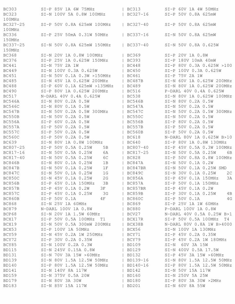
BC303 SI-P 85V 1A 6W 75MHz | BC313 SI-P 60V 1A 4W 50MHz BC323 SI-N 100V 5A 0.8W 100MHz | BC327-16 SI-P 50V 0.8A 625mW100MHz BC327-25 SI-P 50V 0.8A 625mW 100MHz | BC327-40 SI-P 50V 0.8A 625mW100MHz BC336 SI-P 25V 50mA 0.31W 50MHz | BC337-16 SI-N 50V 0.8A 625mW150MHz BC337-25 SI-N 50V 0.8A 625mW 150MHz | BC337-40 SI-N 50V 0.8A 0.625W150MHz BC368 SI-N 20V 1A 0.8W 100MHz | BC369 SI-P 20V 1A 0.8W BC376 SI-P 25V 1A 0.625W 150MHz | BC393 SI-P 180V 10mA 40mW BC441 SI-N 75V 2A 1W | BC448 SI-P 80V 0.3A 0.625W >100 BC449 SI-N 100V 0.3A 0.625W | BC450 SI-P 100V 0.3A 0.625W BC451 SI-N 50V 0.1A 0.3W >150MHz | BC461 SI-P 75V 2A 1W BC485 SI-N 45V 1A 0.625W 200MHz | BC487B SI-N 60V 1A 0.625W 200MHz BC488 SI-P 60V 0.1A 625mW >135MHz | BC489 SI-N 80V 1A 0.625W 200MHz BC490 SI-P 80V 1A 0.625W 200MHz | BC516 P-DARL 40V 0.4A 0.625W BC517 N-DARL 40V 0.4A 0.625W | BC538 SI-N 80V 1A 0.625W 100MHz BC546A SI-N 80V 0.2A 0.5W | BC546B SI-N 80V 0.2A 0.5W BC546C SI-N 80V 0.1A 0.5W | BC547A SI-N 50V 0.2A 0.5W BC547B SI-N 50V 0.2A 0.5W 300MHz | BC547C SI-N 50V 0.2A 0.5W 300MHz BC550B SI-N 50V 0.2A 0.5W | BC550C SI-N 50V 0.2A 0.5W BC556A SI-P 60V 0.2A 0.5W | BC556B SI-P 80V 0.2A 0.5W BC557A SI-P 50V 0.2A 0.5W | BC557B SI-P 50V 0.2A 0.5W BC557C SI-P 50V 0.2A 0.5W | BC560B SI-P 50V 0.2A 0.5W BC560C SI-P 50V 0.2A 0.5W | BC618 N-DARL 80V 1A 0.625W B>10 BC639 SI-N 80V 1A 0.8W 100MHz | BC640 SI-P 80V 1A 0.8W 130MHz BC807-25 SI-P 50V 0.5A 0.25W 5B | BC807-40 SI-P 45V 0.5A 0.3W 100MHz BC817-16 SI-N 50V 0.5A 0.25W 6A | BC817-25 SI-N 50V 0.5A 0.25W 6B BC817-40 SI-N 50V 0.5A 0.25W 6C | BC828 SI-P 50V 0.8A 0.8W 100MHz BC846B SI-N 80V 0.1A 0.25W 1B | BC847A SI-N 50V 0.1A 0.2W BC847B SI-N 50V 0.1A 0.25W 1F | BC847BR SI-N 50V 0.1A 0.25W SMD BC847C SI-N 50V 0,1A 0.25W 1G | BC849C SI-N 30V 0.1A 0.25W 2C BC850C SI-N 45V 0.1A 0.25W 2G | BC856A SI-P 65V 0.1A 150MHz 3A BC856B SI-P 65V 0.1A 150MHz 3B | BC857A SI-P 50V 0.1A 150MHz BC857B SI-P 45V 0.1A 0.2W 3F | BC857BR SI-P 45V 0.1A 0.2W BC857C SI-P 45V 0.1A 0.25W 3G | BC859B SI-P 30V 0.1A 0.25W 4B BC860B SI-P 50V 0.1A 4F | BC860C SI-P 50V 0.1A 4G BC868 SI-N 25V 1A 60MHz | BC869 SI-P 25V 1A 1W 60MHz BC879 N-DARL 100V 1A 0.8W | BC880 P-DARL 100V 1A 0.8W BCP68 SI-N 20V 1A 1.5W 60MHz | BCV27 N-DARL 40V 0.5A 0.25W B>1 BCX17 SI-P 50V 0.5A 100MHz T1 | BCX17R SI-P 50V 0.5A 100MHz T4 BCX19 SI-N 50V 0.5A 300mW 200MHz | BCX38B N-DARL 80V 0.8A 1W B>4000 BCX53 SI-P 100V 1A 50MHz | BCX56 SI-N 100V 1A 130MHz BCY59 SI-N 45V 0.2A 1W 250MHz | BCY71 SI-P 45V 0.2A 0.35W BCY72 SI-P 30V 0.2A 0.35W | BCY79 SI-P 45V 0.2A 1W 180MHz BCY85 SI-N 100V 0.2A 0.3W | BD109 SI-N 60V 3A 15W BD115 SI-N 245V 0.15A 0.8W | BD129 SI-N 400V 0.5A 17.5W BD131 SI-N 70V 3A 15W >60MHz | BD132 SI-P 45V 3A 15W >60MHz BD139 SI-N 80V 1.5A 12.5W 50MHz | BD139-16 SI-N 80V 1.5A 12.5W 50MHz BD140 SI-P 80V 1.5A 12.5W 50MHz | BD140-16 SI-P 80V 1.5A 12.5W 50MHz BD141 SI-N 140V 8A 117W | BD142 SI-N 50V 15A 117W BD159 SI-N 375V 0.5A 20W | BD160 SI-N 250V 5A 25W BD179 SI-N 80V 3A 30W | BD180 SI-P 80V 3A 30W >2MHz BD183 SI-N 85V 15A 117W | BD201 SI-N 60V 8A 55W

BD201F SI-N 60V 8A 32W | BD204F SI-P 60/60V 8A 60W >7MHz BD230 SI-N 100V 1.5A 12.5W | BD231 SI-P 100V 1.5A 12.5W BD232 SI-N 300V 0.25A 7W | BD237 SI-N 100V 2A 25W 3MHz BD238 SI-P 100V 2A 25W 3MHz | BD239C SI-N 100V 2A 30W 3MHz BD240 SI-P 45V 2A 30W | BD240C SI-P 100V 2A 30W 3MHz BD241C SI-N 100V 3A 40W 3MHz | BD241D SI-N 120V 3A 40W 3MHz BD242C SI-P 100V 3A 40W 3MHz | BD243C SI-N 100V 6A 65W 3MHz BD243F SI-N 200V 6A 65W 3MHz | BD244C SI-P 100V 6A 65W 3MHz BD244F SI-P 200V 6A 65W 3MHz | BD250C SI-P 100V 25A 125W 3MHz BD277 SI-P 45V 7A 70W >10MHz | BD302 SI-P 60V 8A 55W >3MHz BD303 SI-N 60V 8A 55W >3MHz | BD314 SI-P 80V 10A 150W BD317 SI-N 100V 16A 200W 1MHz | BD318 SI-P 100V 16A 200W BD329 SI-N 32V 3A 15W 130MHz | BD330 SI-P 32V 3A 15W BD335 N-DARL 100V 6A 60W | BD336 P-DARL 100V 6A 60W BD337 N-DARL+D 120V 6A 60W >10MHz | BD362 SI-P 32V 3A 15W BD371B SI-N 60V 1,5A 2,5W | BD385 SI-N 60V 1A 10W >250MHz BD387 SI-N 80V 1A 10W >250MHz | BD410 SI-N 500V 1A 20W BD411 N-DARL 50V 2A 10W B>25K | BD441 SI-N 80V 4A 36W 3MHz BD442 SI-P 80V 4A 36W 3MHz | BD515 SI-N 45V 2A 10W 160MHz BD537 SI-N 80V 8A 50W | BD538 SI-P 80V 4A 50W >3MHz BD539 SI-N 40V 5A 45W | BD543C SI-N 100V 8A 70W 3MHz BD545 SI-N 40V 15A 85W 3MHz | BD637 SI-N 100V 2A 3OW >3MHz BD638 SI-P 100V 2A 30W >3MHz | BD648 P-DARL 80V 8A 62,5W BD651 N-DARL 120V 8A 62.5W | BD652 P-DARL 120V 8A 62.5W BD679A N-DARL+D 80V 4A 40W | BD680A P-DARL+D 80V 4A 40W BD681 N-DARL+D 100V 4A 40W B>75 | BD682 P-DARL+D 100V 4A 40W BD683 N-DARL 120V 4A 40W | BD684 P-DARL 120V 4A 40W BD711 SI-N 100V 12A 75W | BD712 SI-P 100V 12A 75W POWER BD722 SI-P 80V 4A 36W >3MHz | BD743C SI-N 110V 15A 90W >5MHz BD744C SI-P 110V 15A 90W 5MHz | BD750 SI-P 100V 20A 200W BD751 SI-N 100V 20A 200W | BD791 SI-N 100V 4A 15W BD792 SI-P 100V 4A 15W | BD801 SI-N 100V 8A 65W >3MHz BD829 SI-N 100V 1A 8W | BD830 SI-P 100V 1A 8W 75MHz BD839 SI-N 45V 1.5A 10W 125MHz | BD843 SI-N 100V 1.5A 10W>150MHz BD877 N-DARL 80V 1A 9W 200MHz | BD879 N-DARL 100V 1A 9W 200MHz BD880 P-DARL 100V 1A 200MHz | BD901 N-DARL+D 100V 8A 70W BD902 P-DARL 100V 8A 70W | BD911 SI-N 100V 15A 90W BD912 SI-P 100V 15A 90W | BD939F SI-N 120V 3A 19W 3MHz BD941 SI-N 140V 3A 30W 3MHz | BD942 SI-P 140V 3A 30W 3MHz BD943 SI-N 22V 5A 40W 3MHz | BD948 SI-P 45V 5A 40W 3MHz BD951 SI-N 80V 5A 40W >3MHz | BD956 SI-P 120V 5A 40W 3MHz BDT61 N-DARL+D 60V 4A 50W >10MHz | BDT61C N-DARL+D 120V 4A 50W>10MHz BDT61F N-DARL+D 60V 4A | BDT62C P-DARL 120V 10A 90W B>1K BDT63C N-DARL 120V 10A 90W B>1K | BDT64C P-DARL 120V 12A 125W B>1K BDT65C N-DARL 120V 12A 125W B>1K | BDT85A SI-N 100V 15A 125W 20MHz BDT86A SI-P 100V 15A 125W 20MHz | BDT87 SI-N 120V 15A 125W 10MHz BDT88 SI-P 120V 12A 117W | BDT95A SI-N 100V 10A 90W 4MHz BDT96A SI-P 100V 10A 90W 4MHz | BDV64C P-DARL+D 120V 20A 125W B> BDV65B N-DARL+D 100V 20A 125W B> | BDV65C N-DARL+D 120V 20A 125W B> BDV66C P-DARL+D 120V 16A 200W 7MHz | BDV66D P-DARL+D 160V 16A 200W BDW22C SI-P 100V 10A 90W >3MHz | BDW23C N-DARL+D 100V 6A 50W BDW42 N-DARL 100V 15A 85W B>1K | BDW46 P-DARL 80V 15A 85W B>1K BDW47 P-DARL 100V 15A 85W B>1K | BDW51C SI-N 100V 15A 125W >3MHz
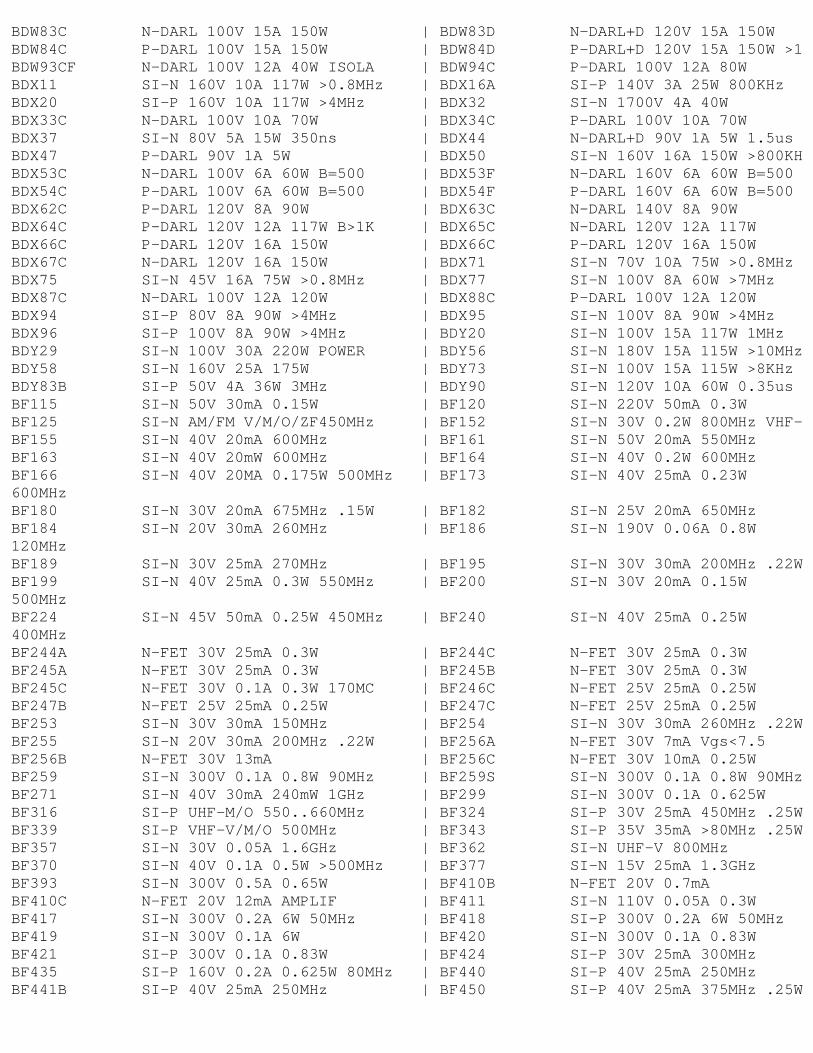
BDW83C N-DARL 100V 15A 150W | BDW83D N-DARL+D 120V 15A 150W BDW84C P-DARL 100V 15A 150W | BDW84D P-DARL+D 120V 15A 150W >1 BDW93CF N-DARL 100V 12A 40W ISOLA | BDW94C P-DARL 100V 12A 80W BDX11 SI-N 160V 10A 117W >0.8MHz | BDX16A SI-P 140V 3A 25W 800KHz BDX20 SI-P 160V 10A 117W >4MHz | BDX32 SI-N 1700V 4A 40W BDX33C N-DARL 100V 10A 70W | BDX34C P-DARL 100V 10A 70W BDX37 SI-N 80V 5A 15W 350ns | BDX44 N-DARL+D 90V 1A 5W 1.5us BDX47 P-DARL 90V 1A 5W | BDX50 SI-N 160V 16A 150W >800KH BDX53C N-DARL 100V 6A 60W B=500 | BDX53F N-DARL 160V 6A 60W B=500 BDX54C P-DARL 100V 6A 60W B=500 | BDX54F P-DARL 160V 6A 60W B=500 BDX62C P-DARL 120V 8A 90W | BDX63C N-DARL 140V 8A 90W BDX64C P-DARL 120V 12A 117W B>1K | BDX65C N-DARL 120V 12A 117W BDX66C P-DARL 120V 16A 150W | BDX66C P-DARL 120V 16A 150W BDX67C N-DARL 120V 16A 150W | BDX71 SI-N 70V 10A 75W >0.8MHz BDX75 SI-N 45V 16A 75W >0.8MHz | BDX77 SI-N 100V 8A 60W >7MHz BDX87C N-DARL 100V 12A 120W | BDX88C P-DARL 100V 12A 120W BDX94 SI-P 80V 8A 90W >4MHz | BDX95 SI-N 100V 8A 90W >4MHz BDX96 SI-P 100V 8A 90W >4MHz | BDY20 SI-N 100V 15A 117W 1MHz BDY29 SI-N 100V 30A 220W POWER | BDY56 SI-N 180V 15A 115W >10MHz BDY58 SI-N 160V 25A 175W | BDY73 SI-N 100V 15A 115W >8KHz BDY83B SI-P 50V 4A 36W 3MHz | BDY90 SI-N 120V 10A 60W 0.35us BF115 SI-N 50V 30mA 0.15W | BF120 SI-N 220V 50mA 0.3W BF125 SI-N AM/FM V/M/O/ZF450MHz | BF152 SI-N 30V 0.2W 800MHz VHF- BF155 SI-N 40V 20mA 600MHz | BF161 SI-N 50V 20mA 550MHz BF163 SI-N 40V 20mW 600MHz | BF164 SI-N 40V 0.2W 600MHz BF166 SI-N 40V 20MA 0.175W 500MHz | BF173 SI-N 40V 25mA 0.23W600MHz BF180 SI-N 30V 20mA 675MHz .15W | BF182 SI-N 25V 20mA 650MHz BF184 SI-N 20V 30mA 260MHz | BF186 SI-N 190V 0.06A 0.8W120MHz BF189 SI-N 30V 25mA 270MHz | BF195 SI-N 30V 30mA 200MHz .22W BF199 SI-N 40V 25mA 0.3W 550MHz | BF200 SI-N 30V 20mA 0.15W500MHz BF224 SI-N 45V 50mA 0.25W 450MHz | BF240 SI-N 40V 25mA 0.25W400MHz BF244A N-FET 30V 25mA 0.3W | BF244C N-FET 30V 25mA 0.3W BF245A N-FET 30V 25mA 0.3W | BF245B N-FET 30V 25mA 0.3W BF245C N-FET 30V 0.1A 0.3W 170MC | BF246C N-FET 25V 25mA 0.25W BF247B N-FET 25V 25mA 0.25W | BF247C N-FET 25V 25mA 0.25W BF253 SI-N 30V 30mA 150MHz | BF254 SI-N 30V 30mA 260MHz .22W BF255 SI-N 20V 30mA 200MHz .22W | BF256A N-FET 30V 7mA Vgs<7.5 BF256B N-FET 30V 13mA | BF256C N-FET 30V 10mA 0.25W BF259 SI-N 300V 0.1A 0.8W 90MHz | BF259S SI-N 300V 0.1A 0.8W 90MHz BF271 SI-N 40V 30mA 240mW 1GHz | BF299 SI-N 300V 0.1A 0.625W BF316 SI-P UHF-M/O 550..660MHz | BF324 SI-P 30V 25mA 450MHz .25W BF339 SI-P VHF-V/M/O 500MHz | BF343 SI-P 35V 35mA >80MHz .25W BF357 SI-N 30V 0.05A 1.6GHz | BF362 SI-N UHF-V 800MHz BF370 SI-N 40V 0.1A 0.5W >500MHz | BF377 SI-N 15V 25mA 1.3GHz BF393 SI-N 300V 0.5A 0.65W | BF410B N-FET 20V 0.7mA BF410C N-FET 20V 12mA AMPLIF | BF411 SI-N 110V 0.05A 0.3W BF417 SI-N 300V 0.2A 6W 50MHz | BF418 SI-P 300V 0.2A 6W 50MHz BF419 SI-N 300V 0.1A 6W | BF420 SI-N 300V 0.1A 0.83W BF421 SI-P 300V 0.1A 0.83W | BF424 SI-P 30V 25mA 300MHz BF435 SI-P 160V 0.2A 0.625W 80MHz | BF440 SI-P 40V 25mA 250MHz BF441B SI-P 40V 25mA 250MHz | BF450 SI-P 40V 25mA 375MHz .25W
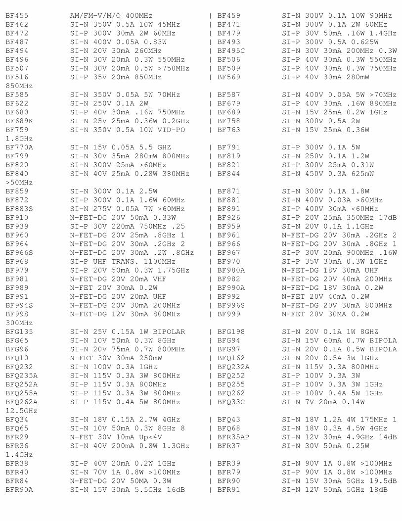
BF455 AM/FM-V/M/O 400MHz | BF459 SI-N 300V 0.1A 10W 90MHz BF462 SI-N 350V 0.5A 10W 45MHz | BF471 SI-N 300V 0.1A 2W 60MHz BF472 SI-P 300V 30mA 2W 60MHz | BF479 SI-P 30V 50mA .16W 1.4GHz BF487 SI-N 400V 0.05A 0.83W | BF493 SI-P 300V 0.5A 0.625W BF494 SI-N 20V 30mA 260MHz | BF495C SI-N 30V 30mA 200MHz 0.3W BF496 SI-N 30V 20mA 0.3W 550MHz | BF506 SI-P 40V 30mA 0.3W 550MHz BF507 SI-N 30V 20mA 0.5W >750MHz | BF509 SI-P 40V 30mA 0.3W 750MHz BF516 SI-P 35V 20mA 850MHz | BF569 SI-P 40V 30mA 280mW850MHz BF585 SI-N 350V 0.05A 5W 70MHz | BF587 SI-N 400V 0.05A 5W >70MHz BF622 SI-N 250V 0.1A 2W | BF679 SI-P 40V 30mA .16W 880MHz BF680 SI-P 40V 30mA .16W 750MHz | BF689 SI-N 15V 25mA 0.2W 1GHz BF689K SI-N 25V 25mA 0.36W 0.2GHz | BF758 SI-N 300V 0.5A 2W BF759 SI-N 350V 0.5A 10W VID-PO | BF763 SI-N 15V 25mA 0.36W1.8GHz BF770A SI-N 15V 0.05A 5.5 GHZ | BF791 SI-P 300V 0.1A 5W BF799 SI-N 30V 35mA 280mW 800MHz | BF819 SI-N 250V 0.1A 1.2W BF820 SI-N 300V 25mA >60MHz | BF821 SI-P 300V 25mA 0.31W BF840 SI-N 40V 25mA 0.28W 380MHz | BF844 SI-N 450V 0.3A 625mW>50MHz BF859 SI-N 300V 0.1A 2.5W | BF871 SI-N 300V 0.1A 1.8W BF872 SI-P 300V 0.1A 1.6W 60MHz | BF881 SI-N 400V 0.03A >60MHz BF883S SI-N 275V 0.05A 7W >60MHz | BF891 SI-P 400V 30mA <60MHz BF910 N-FET-DG 20V 50mA 0.33W | BF926 SI-P 20V 25mA 350MHz 17dB BF939 SI-P 30V 220mA 750MHz .25 | BF959 SI-N 20V 0.1A 1.1GHz BF960 N-FET-DG 20V 25mA .8GHz 1 | BF961 N-FET-DG 20V 30mA .2GHz 2 BF964 N-FET-DG 20V 30mA .2GHz 2 | BF966 N-FET-DG 20V 30mA .8GHz 1 BF966S N-FET-DG 20V 30mA .2W .8GHz | BF967 SI-P 30V 20mA 900MHz .16W BF968 SI-P UHF TRANS. 1100MHz | BF970 SI-P 35V 30mA 0.3W 1GHz BF979 SI-P 20V 50mA 0.3W 1.75GHz | BF980A N-FET-DG 18V 30mA UHF BF981 N-FET-DG 20V 20mA VHF | BF982 N-FET-DG 20V 40mA 200MHz BF989 N-FET 20V 30mA 0.2W | BF990A N-FET-DG 18V 30mA 0.2W BF991 N-FET-DG 20V 20mA UHF | BF992 N-FET 20V 40mA 0.2W BF994S N-FET-DG 20V 30mA 200MHz | BF996S N-FET-DG 20V 30mA 800MHz BF998 N-FET-DG 12V 30mA 800MHz | BF999 N-FET 20V 30MA 0.2W300MHz BFG135 SI-N 25V 0.15A 1W BIPOLAR | BFG198 SI-N 20V 0.1A 1W 8GHZ BFG65 SI-N 10V 50mA 0.3W 8GHz | BFG94 SI-N 15V 60mA 0.7W BIPOLA BFG96 SI-N 20V 75mA 0.7W 800MHz | BFG97 SI-N 20V 0.1A 0.5W BIPOLA BFQ10 N-FET 30V 30mA 250mW | BFQ162 SI-N 20V 0.5A 3W 1GHz BFQ232 SI-N 100V 0.3A 1GHz | BFQ232A SI-N 115V 0.3A 800MHz BFQ235A SI-N 115V 0.3A 3W 800MHz | BFQ252 SI-P 100V 0.3A 3W BFQ252A SI-P 115V 0.3A 800MHz | BFQ255 SI-P 100V 0.3A 3W 1GHz BFQ255A SI-P 115V 0.3A 3W 800MHz | BFQ262 SI-P 100V 0.4A 5W 1GHz BFQ262A SI-P 115V 0.4A 5W 800MHz | BFQ33C SI-N 7V 20mA 0.14W12.5GHz BFQ34 SI-N 18V 0.15A 2.7W 4GHz | BFQ43 SI-N 18V 1.2A 4W 175MHz 1 BFQ65 SI-N 10V 50mA 0.3W 8GHz 8 | BFQ68 SI-N 18V 0.3A 4.5W 4GHz BFR29 N-FET 30V 10mA Up<4V | BFR35AP SI-N 12V 30mA 4.9GHz 14dB BFR36 SI-N 40V 200mA 0.8W 1.3GHz | BFR37 SI-N 30V 50mA 0.25W1.4GHz BFR38 SI-P 40V 20mA 0.2W 1GHz | BFR39 SI-N 90V 1A 0.8W >100MHz BFR40 SI-N 70V 1A 0.8W >100MHz | BFR79 SI-P 90V 1A 0.8W >100MHz BFR84 N-FET-DG 20V 50MA 0.3W | BFR90 SI-N 15V 30mA 5GHz 19.5dB BFR90A SI-N 15V 30mA 5.5GHz 16dB | BFR91 SI-N 12V 50mA 5GHz 18dB
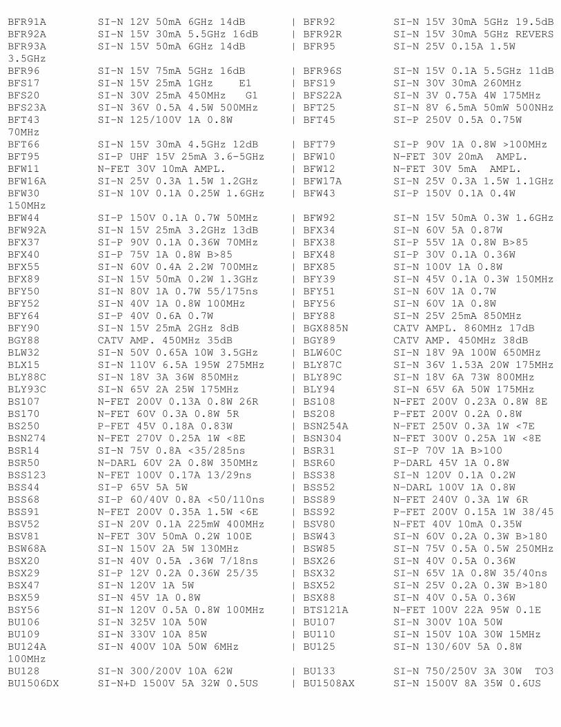
BFR91A SI-N 12V 50mA 6GHz 14dB | BFR92 SI-N 15V 30mA 5GHz 19.5dB BFR92A SI-N 15V 30mA 5.5GHz 16dB | BFR92R SI-N 15V 30mA 5GHz REVERS BFR93A SI-N 15V 50mA 6GHz 14dB | BFR95 SI-N 25V 0.15A 1.5W3.5GHz BFR96 SI-N 15V 75mA 5GHz 16dB | BFR96S SI-N 15V 0.1A 5.5GHz 11dB BFS17 SI-N 15V 25mA 1GHz E1 | BFS19 SI-N 30V 30mA 260MHz BFS20 SI-N 30V 25mA 450MHz G1 | BFS22A SI-N 3V 0.75A 4W 175MHz BFS23A SI-N 36V 0.5A 4.5W 500MHz | BFT25 SI-N 8V 6.5mA 50mW 500NHz BFT43 SI-N 125/100V 1A 0.8W | BFT45 SI-P 250V 0.5A 0.75W70MHz BFT66 SI-N 15V 30mA 4.5GHz 12dB | BFT79 SI-P 90V 1A 0.8W >100MHz BFT95 SI-P UHF 15V 25mA 3.6-5GHz | BFW10 N-FET 30V 20mA AMPL. BFW11 N-FET 30V 10mA AMPL. | BFW12 N-FET 30V 5mA AMPL. BFW16A SI-N 25V 0.3A 1.5W 1.2GHz | BFW17A SI-N 25V 0.3A 1.5W 1.1GHz BFW30 SI-N 10V 0.1A 0.25W 1.6GHz | BFW43 SI-P 150V 0.1A 0.4W150MHz BFW44 SI-P 150V 0.1A 0.7W 50MHz | BFW92 SI-N 15V 50mA 0.3W 1.6GHz BFW92A SI-N 15V 25mA 3.2GHz 13dB | BFX34 SI-N 60V 5A 0.87W BFX37 SI-P 90V 0.1A 0.36W 70MHz | BFX38 SI-P 55V 1A 0.8W B>85 BFX40 SI-P 75V 1A 0.8W B>85 | BFX48 SI-P 30V 0.1A 0.36W BFX55 SI-N 60V 0.4A 2.2W 700MHz | BFX85 SI-N 100V 1A 0.8W BFX89 SI-N 15V 50mA 0.2W 1.3GHz | BFY39 SI-N 45V 0.1A 0.3W 150MHz BFY50 SI-N 80V 1A 0.7W 55/175ns | BFY51 SI-N 60V 1A 0.7W BFY52 SI-N 40V 1A 0.8W 100MHz | BFY56 SI-N 60V 1A 0.8W BFY64 SI-P 40V 0.6A 0.7W | BFY88 SI-N 25V 25mA 850MHz BFY90 SI-N 15V 25mA 2GHz 8dB | BGX885N CATV AMPL. 860MHz 17dB BGY88 CATV AMP. 450MHz 35dB | BGY89 CATV AMP. 450MHz 38dB BLW32 SI-N 50V 0.65A 10W 3.5GHz | BLW60C SI-N 18V 9A 100W 650MHz BLX15 SI-N 110V 6.5A 195W 275MHz | BLY87C SI-N 36V 1.53A 20W 175MHz BLY88C SI-N 18V 3A 36W 850MHz | BLY89C SI-N 18V 6A 73W 800MHz BLY93C SI-N 65V 2A 25W 175MHz | BLY94 SI-N 65V 6A 50W 175MHz BS107 N-FET 200V 0.13A 0.8W 26R | BS108 N-FET 200V 0.23A 0.8W 8E BS170 N-FET 60V 0.3A 0.8W 5R | BS208 P-FET 200V 0.2A 0.8W BS250 P-FET 45V 0.18A 0.83W | BSN254A N-FET 250V 0.3A 1W <7E BSN274 N-FET 270V 0.25A 1W <8E | BSN304 N-FET 300V 0.25A 1W <8E BSR14 SI-N 75V 0.8A <35/285ns | BSR31 SI-P 70V 1A B>100 BSR50 N-DARL 60V 2A 0.8W 350MHz | BSR60 P-DARL 45V 1A 0.8W BSS123 N-FET 100V 0.17A 13/29ns | BSS38 SI-N 120V 0.1A 0.2W BSS44 SI-P 65V 5A 5W | BSS52 N-DARL 100V 1A 0.8W BSS68 SI-P 60/40V 0.8A <50/110ns | BSS89 N-FET 240V 0.3A 1W 6R BSS91 N-FET 200V 0.35A 1.5W <6E | BSS92 P-FET 200V 0.15A 1W 38/45 BSV52 SI-N 20V 0.1A 225mW 400MHz | BSV80 N-FET 40V 10mA 0.35W BSV81 N-FET 30V 50mA 0.2W 100E | BSW43 SI-N 60V 0.2A 0.3W B>180 BSW68A SI-N 150V 2A 5W 130MHz | BSW85 SI-N 75V 0.5A 0.5W 250MHz BSX20 SI-N 40V 0.5A .36W 7/18ns | BSX26 SI-N 40V 0.5A 0.36W BSX29 SI-P 12V 0.2A 0.36W 25/35 | BSX32 SI-N 65V 1A 0.8W 35/40ns BSX47 SI-N 120V 1A 5W | BSX52 SI-N 25V 0.2A 0.3W B>180 BSX59 SI-N 45V 1A 0.8W | BSX88 SI-N 40V 0.5A 0.36W BSY56 SI-N 120V 0.5A 0.8W 100MHz | BTS121A N-FET 100V 22A 95W 0.1E BU106 SI-N 325V 10A 50W | BU107 SI-N 300V 10A 50W BU109 SI-N 330V 10A 85W | BU110 SI-N 150V 10A 30W 15MHz BU124A SI-N 400V 10A 50W 6MHz | BU125 SI-N 130/60V 5A 0.8W100MHz BU128 SI-N 300/200V 10A 62W | BU133 SI-N 750/250V 3A 30W TO3 BU1506DX SI-N+D 1500V 5A 32W 0.5US | BU1508AX SI-N 1500V 8A 35W 0.6US
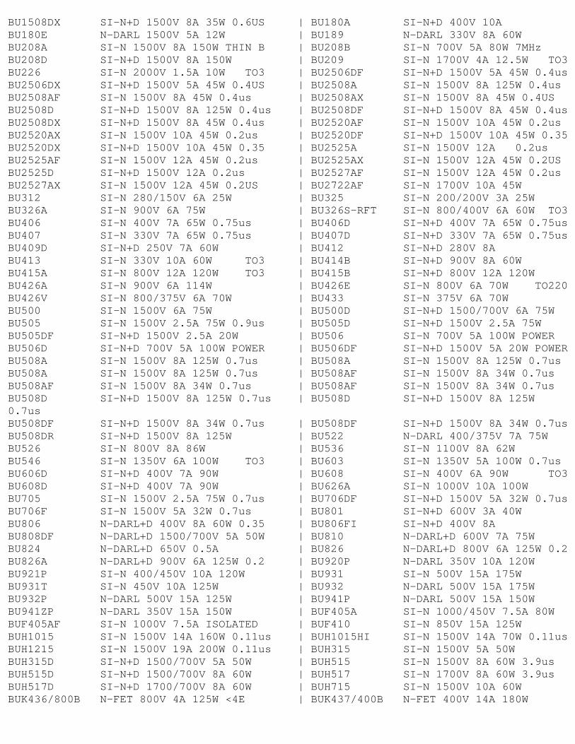
BU1508DX SI-N+D 1500V 8A 35W 0.6US | BU180A SI-N+D 400V 10A BU180E N-DARL 1500V 5A 12W | BU189 N-DARL 330V 8A 60W BU208A SI-N 1500V 8A 150W THIN B | BU208B SI-N 700V 5A 80W 7MHz BU208D SI-N+D 1500V 8A 150W | BU209 SI-N 1700V 4A 12.5W TO3 BU226 SI-N 2000V 1.5A 10W TO3 | BU2506DF SI-N+D 1500V 5A 45W 0.4us BU2506DX SI-N+D 1500V 5A 45W 0.4US | BU2508A SI-N 1500V 8A 125W 0.4us BU2508AF SI-N 1500V 8A 45W 0.4us | BU2508AX SI-N 1500V 8A 45W 0.4US BU2508D SI-N+D 1500V 8A 125W 0.4us | BU2508DF SI-N+D 1500V 8A 45W 0.4us BU2508DX SI-N+D 1500V 8A 45W 0.4us | BU2520AF SI-N 1500V 10A 45W 0.2us BU2520AX SI-N 1500V 10A 45W 0.2us | BU2520DF SI-N+D 1500V 10A 45W 0.35 BU2520DX SI-N+D 1500V 10A 45W 0.35 | BU2525A SI-N 1500V 12A 0.2us BU2525AF SI-N 1500V 12A 45W 0.2us | BU2525AX SI-N 1500V 12A 45W 0.2US BU2525D SI-N+D 1500V 12A 0.2us | BU2527AF SI-N 1500V 12A 45W 0.2us BU2527AX SI-N 1500V 12A 45W 0.2US | BU2722AF SI-N 1700V 10A 45W BU312 SI-N 280/150V 6A 25W | BU325 SI-N 200/200V 3A 25W BU326A SI-N 900V 6A 75W | BU326S-RFT SI-N 800/400V 6A 60W TO3 BU406 SI-N 400V 7A 65W 0.75us | BU406D SI-N+D 400V 7A 65W 0.75us BU407 SI-N 330V 7A 65W 0.75us | BU407D SI-N+D 330V 7A 65W 0.75us BU409D SI-N+D 250V 7A 60W | BU412 SI-N+D 280V 8A BU413 SI-N 330V 10A 60W TO3 | BU414B SI-N+D 900V 8A 60W BU415A SI-N 800V 12A 120W TO3 | BU415B SI-N+D 800V 12A 120W BU426A SI-N 900V 6A 114W | BU426E SI-N 800V 6A 70W TO220 BU426V SI-N 800/375V 6A 70W | BU433 SI-N 375V 6A 70W BU500 SI-N 1500V 6A 75W | BU500D SI-N+D 1500/700V 6A 75W BU505 SI-N 1500V 2.5A 75W 0.9us | BU505D SI-N+D 1500V 2.5A 75W BU505DF SI-N+D 1500V 2.5A 20W | BU506 SI-N 700V 5A 100W POWER BU506D SI-N+D 700V 5A 100W POWER | BU506DF SI-N+D 1500V 5A 20W POWER BU508A SI-N 1500V 8A 125W 0.7us | BU508A SI-N 1500V 8A 125W 0.7us BU508A SI-N 1500V 8A 125W 0.7us | BU508AF SI-N 1500V 8A 34W 0.7us BU508AF SI-N 1500V 8A 34W 0.7us | BU508AF SI-N 1500V 8A 34W 0.7us BU508D SI-N+D 1500V 8A 125W 0.7us | BU508D SI-N+D 1500V 8A 125W0.7us BU508DF SI-N+D 1500V 8A 34W 0.7us | BU508DF SI-N+D 1500V 8A 34W 0.7us BU508DR SI-N+D 1500V 8A 125W | BU522 N-DARL 400/375V 7A 75W BU526 SI-N 800V 8A 86W | BU536 SI-N 1100V 8A 62W BU546 SI-N 1350V 6A 100W TO3 | BU603 SI-N 1350V 5A 100W 0.7us BU606D SI-N+D 400V 7A 90W | BU608 SI-N 400V 6A 90W TO3 BU608D SI-N+D 400V 7A 90W | BU626A SI-N 1000V 10A 100W BU705 SI-N 1500V 2.5A 75W 0.7us | BU706DF SI-N+D 1500V 5A 32W 0.7us BU706F SI-N 1500V 5A 32W 0.7us | BU801 SI-N+D 600V 3A 40W BU806 N-DARL+D 400V 8A 60W 0.35 | BU806FI SI-N+D 400V 8A BU808DF N-DARL+D 1500/700V 5A 50W | BU810 N-DARL+D 600V 7A 75W BU824 N-DARL+D 650V 0.5A | BU826 N-DARL+D 800V 6A 125W 0.2 BU826A N-DARL+D 900V 6A 125W 0.2 | BU920P N-DARL 350V 10A 120W BU921P SI-N 400/450V 10A 120W | BU931 SI-N 500V 15A 175W BU931T SI-N 450V 10A 125W | BU932 N-DARL 500V 15A 175W BU932P N-DARL 500V 15A 125W | BU941P N-DARL 500V 15A 150W BU941ZP N-DARL 350V 15A 150W | BUF405A SI-N 1000/450V 7.5A 80W BUF405AF SI-N 1000V 7.5A ISOLATED | BUF410 SI-N 850V 15A 125W BUH1015 SI-N 1500V 14A 160W 0.11us | BUH1015HI SI-N 1500V 14A 70W 0.11us BUH1215 SI-N 1500V 19A 200W 0.11us | BUH315 SI-N 1500V 5A 50W BUH315D SI-N+D 1500/700V 5A 50W | BUH515 SI-N 1500V 8A 60W 3.9us BUH515D SI-N+D 1500/700V 8A 60W | BUH517 SI-N 1700V 8A 60W 3.9us BUH517D SI-N+D 1700/700V 8A 60W | BUH715 SI-N 1500V 10A 60W BUK436/800B N-FET 800V 4A 125W <4E | BUK437/400B N-FET 400V 14A 180W
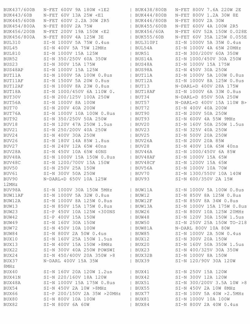
BUK437/600B N-FET 600V 9A 180W <1E2 | BUK438/800B N-FET 800V 7.6A 220W 2E BUK443/60B N-FET 60V 13A 25W <E1 | BUK444/800B N-FET 800V 1.2A 30W 8E BUK445/600B N-FET 600V 2.2A 30W 2R5 | BUK446/800B N-FET 800V 2A 30W BUK454/800A N-FET 800V 2A 75W | BUK455/600B N-FET 600V 4A 100W 2R5 BUK456/200B N-FET 200V 19A 150W <E2 | BUK456/60A N-FET 60V 52A 150W 0.028E BUK456/800A N-FET 800V 4A 125W 3E | BUK555/60B N-FET 60V 35A 125W 0.055E BUL310 SI-N 1000V 5A 75W 0.4us | BUL310PI SI-N 1000V 5A 35W 0.4us BUL45 SI-N 400V 5A 75W 12MHz | BUL54A SI-N 1000V 4A 65W 20MHz BUL810 SI-N 1000V 15A 125W | BUR51 SI-N 300/200V 60A 350W BUR52 SI-N 350/250V 60A 350W | BUS14A SI-N 1000/450V 30A 250W BUS23 SI-N 300V 15A 175W | BUS48A SI-N 1000V 15A 175W BUS48AP SI-N 1000V 15A 125W | BUS98A SI-N 450V 30A 250W BUT11A SI-N 1000V 5A 100W 0.8us | BUT11A SI-N 1000V 5A 100W 0.8us BUT11AF SI-N 1500V 5A 20W 0.8us | BUT12A SI-N 1000V 8A 125W 0.8us BUT12AF SI-N 1000V 8A 23W 0.8us | BUT13 N-DARL+D 400V 28A 175W BUT18A SI-N 1000/450V 6A 110W 0. | BUT18AF SI-N 1000V 6A 33W 0.8us BUT30V SI-N 200/125V 100A 250W | BUT34 N-DARL+D 850V 50A 250W BUT56A SI-N 1000V 8A 100W | BUT57 N-DARL+D 400V 15A 110W B> BUT70 SI-N 200V 40A 200W | BUT72 SI-N 400V 40A 200W BUT76A SI-N 1000V 10A 100W 0.8us | BUT90 SI-N 200V 50A 250W BUT92 SI-N 350/250V 50A 250W | BUT93 SI-N 600V 4A 55W 9MHz BUV18 SI-N 120V 47A 250W 1.5us | BUV20 SI-N 160V 50A 250W 1.5us BUV21 SI-N 250/200V 40A 250W | BUV23 SI-N 325V 40A 250W BUV24 SI-N 400V 30A 250W | BUV25 SI-N 500V 20A 250W BUV26 SI-N 180V 14A 85W 1.8us | BUV26A SI-N 200V 20A 85W BUV27 SI-N 240V 12A 65W 40ns | BUV28 SI-N 400V 10A 65W 40ns BUV28A SI-N 450V 10A 65W 40NS | BUV46A SI-N 1000/450V 6A 85W BUV48A SI-N 1000V 15A 150W 0.8us | BUV48AF SI-N 1000V 15A 65W BUV48C SI-N 1200/700V 15A 150W | BUV48CF SI-N 1200V 15A 65W BUV50 SI-N 250V 25A 150W | BUV56A SI-N 1000V 10A 70W BUV61 SI-N 300V 50A 250W | BUV70 SI-N 1300/550V 10A 140W BUV90 N-DARL+D 650V 10A 125W | BUV93 SI-N 600/350V 2A 15W12MHz BUV98A SI-N 1000V 30A 150W 5MHz | BUW11A SI-N 1000V 5A 100W 0.8us BUW11AF SI-N 1000V 5A 32W 0.8us | BUW12 SI-N 850V 8A 125W 0.8us BUW12A SI-N 1000V 8A 125W 0.8us | BUW12F SI-N 850V 8A 34W 0.8us BUW13 SI-N 850V 15A 175W 0.8us | BUW13A SI-N 1000V 15A 175W 0.8us BUW23 SI-P 450V 10A 125W <300NS | BUW26 SI-N 800V 10A 125W 20MHz BUW42 SI-P 400V 15A 150W | BUW48 SI-N 120V 30A 150W 1.5us BUW49 SI-N 160V 30A 150W | BUW50 SI-N 250V 25A 150W TO-218 BUW72 SI-N 450V 10A 100W | BUW81A N-DARL 800V 10A 80W BUW84 SI-N 800V 2A 50W 0.4us | BUW85 SI-N 1000V 2A 50W 0.4us BUX10 SI-N 160V 25A 150W 1.5us | BUX12 SI-N 300V 20A 150W BUX13 SI-N 400V 15A 150W >8MHz | BUX20 SI-N 160V 50A 350W 1.5us BUX22 SI-N 300V 40A 250W POWSWI | BUX23 SI-N 400/325V 30A 350W BUX24 SI-N 450/400V 20A 350W >8 | BUX32B SI-N 1000V 8A 150W BUX37 N-DARL 400V 15A 35W | BUX39 SI-N 120/90V 30A 120W8MHz BUX40 SI-N 160V 20A 120W 1.2us | BUX41 SI-N 250V 15A 120W BUX41N SI-N 220/160V 18A 120W | BUX42 SI-N 300V 12A 120W BUX48A SI-N 1000V 15A 175W 0.8us | BUX51 SI-N 300/200V 3.5A 10W >8 BUX54 SI-N 450V 2A 10W >8MHz | BUX55 SI-N 450V 2A 10W 8MHz BUX66 SI-P 200/150V 2A 35W >20MHz | BUX77 SI-N 100V 5A 40W >2.5MHz BUX80 SI-N 800V 10A 100W | BUX81 SI-N 1000V 10A 100W BUX82 SI-N 800V 6A 60W | BUX84 SI-N 800V 2A 40W 0.4us
BUX85 SI-N 1000V 2A 40W 0.4us | BUX85F SI-N 1000V 2A 18W 0.4us BUX86P SI-N 800V 0.5A 20W 0.4us | BUX87 SI-N 1000V 0.5A 20W 0.4us BUX87P SI-N 1000V 0.5A 20W 0.4us | BUX88 SI-N 1500V 12A 160W 7MHz BUX98A SI-N 450V 30A 250W | BUX98C SI-N 1200V 30A 250W 5MHz BUY18S SI-N 80/40V 10A 20W | BUY47 SI-N 150/120V 7A 10W90MHz BUY49P SI-N 250V 3A 10W | BUY49S SI-N 250V 3A 10W 50MHz BUY69A SI-N 1000V 10A 100W 1us | BUY70A SI-N 1000/400V 10A 75W BUY71 SI-N 2200V 2A 40W HORDEFL | BUY72 SI-N 280/200V 10A 60W BUY89 SI-N 1500V 6A 80W | BUZ10 N-FET 50V 20A 80W 0.08R BUZ100 N-FET 50V 60A 250W 0.18E | BUZ11 N-FET 50V 36A BUZ11A N-FET 50V 27A 90W 0.055R | BUZ14 N-FET 50V 39A 125W BUZ15 N-FET 50V 45A 125W | BUZ171 P-FET 50V 8A 40W 0.3R BUZ21 N-FET 100V 21A | BUZ215 N-FET 500V 5A 75W <1E5 BUZ22 N-FET 100V 34A 125W 0.055 | BUZ30A N-FET 200V 7A 75W BUZ310 N-FET 1000V 2.5A 75W <5E | BUZ325 N-FET 400V 12.5A 125W <E3 BUZ326 N-FET 400V 10.5A 125W | BUZ330 N-FET 500V 9.5A 125W 0E6 BUZ332 N-FET 600V 8.5A 150W 0.8R | BUZ332A N-FET 600V 8A 150W 0.9E BUZ338 N-FET 500V 13.5A 180W <E4 | BUZ341 N-FET 200V 33A 170W 0.07E BUZ345 N-FET 100V 41A 150W <E045 | BUZ349 N-FET 100V 32A 125W BUZ380 N-FET 1000V 5.5A 125W 140 | BUZ384 N-FET 500V 10.5A 125W BUZ50A N-FET 1000V 2.5A 75W 5E | BUZ71 N-FET 50V 18A 80W 0.1R BUZ71AF N-FET 50V 11A 35W 0.12R | BUZ72A N-FET 100V 11A BUZ72AF N-FET 100V 10A 40W ISOLAT | BUZ73 N-FET 200V 7A 40W 0.4R BUZ73A N-FET 200V 5.8A 40W 0.6R | BUZ90 N-FET 600V 4.5A 70W <1E6 BUZ900 N-FET 160V 8A 125W | BUZ901 N-FET 200V 8A 125W BUZ905 P-FET 160V 8A 125W | BUZ906 P-FET 200V 8A 125W BUZ90A N-FET 600V 4A 75W 2R | BUZ90AF N-FET 600V 4.3A 75W BUZ91A N-FET 600V 8A 150W 0.9R | BUZ93 N-FET 600V 3.6A 80W <2E5 CA3018 DARLINGTON BJT ARRAY | D44H11 SI-N 80V 10A 50W 50MHz D44H8 SI-N 60V 10A 50W | D45H11 SI-N 80V 10A 50W 0.5us DTA114EK SI-P 50V 0.1A 0.2W 10K/10 | DTA114ES SI-P 50V 0.1A 10K/10KOHM DTA114TL SI-P 50V 0.1A 10KOHM | DTA114YL SI-P 50V 0.1A 10K/47KOHM DTA124ES SI-P 50V 0.1A 22K/22KOHM | DTA124XS SI-P 50V 0.1A 22K/47KOHM DTA143EK SI-P 50V 0.1A 0.2W 47/47K | DTA143ES SI-P 50V 0.1A 4K7/4K7OHM DTA144EK SI-P 50V 0.1A 0.2W 47K/47 | DTA144ES SI-P 50V 0.1A 47K/47K DTA144TS SI-P 50V 0.1A 0.3W Rb=47K | DTC114ES SI-N 50V 0.1A 10K/10KOHM DTC114TS SI-N 50V 0.1A 10K | DTC114YS SI-N 50V 0.1A 10K/47K DTC124EK SI-N 50V 0.1A 0.2W 22/22K | DTC124ES SI-N 50V 0.1A 22K/22KOHM DTC143EK SI-N 50V 0.1A 0.2W 4K7/4K | DTC143ES SI-N 50V 0.1A 4K7/4K7OHM DTC143TS SI-N 50V 0.1A 4K7OHM | DTC143XS SI-N 50V 0.1A 0.3W 4.7K/1 DTC144EK SI-N 50V 0.1A 0.2W 47/47K | DTC144ES SI-N 50V 0.1A 47K/47KOHM DTC144EU SI-N 50V 0.1A 0.2W 47/47K | DTC144TS SI-N 50V 0.1A 0.3W 47KOhm DTC144WS SI-N 50V 0.1A 0.2W 47/22K | ESM6045DV N-DARL+D 450V 84A 250W FT5754M DARLINGTON ARRAY | FT5764M DARLINGTON ARRAY GD243 GE-P 65V 3A 10W | GT20D101 N-IGBT 250V 20A 180W GT20D201 P-IGBT 250V 20A 250W | H6N80 N-FET 800V 4.2A 170W 1E9 HPA100R SI-N+D 1500V 10A 150W 0.2 | HPA150R SI-N+D 1500V 15A 180W 0.2 IR2403 DARL.ARRAY 7x45V 0.4A | IR2422 7XDARLINGTON TRAN. ARRAY IRF120 N-FET 100V 9.2A 60W <58/5 | IRF140 N-FET 100V 28A 150W 0E77 IRF230 N-FET 200V 9A 75W <0E4 | IRF240 N-FET 200V 18A 125W IRF250 N-FET 200V 30A 150W | IRF330 N-FET 400V 5.5A 75W <1E IRF340 N-FET 400V 10A 125W <62/1 | IRF350 N-FET 400V 13A 150W 0.4E IRF440 N-FET 500V 8A 125W <0E85 | IRF450 N-FET 500V 13A 150W IRF520 N-FET 100V 10A 70W 0.27R | IRF530 N-FET 100V 16A 90W 0.16R
IRF540 N-FET 100V 28A 150W 0.077 | IRF630 N-FET 200V 9A 75W 0.4E IRF640 N-FET 200V 18A 125W 0.18R | IRF644 N-FET 250V 14A 125W <E28 IRF730 N-FET 400V 5.5A 100W 1.0R | IRF740 N-FET 400V 10A 125W 0.55R IRF740F N-FET 400V 5.5A 40W <E55 | IRF820 N-FET 500V 3A 75W 3.0R IRF830 N-FET 500V 4.5A 100W 1.5R | IRF830F N-FET 500V 3A 35W 1.5R IRF840 N-FET 500V 4.5A 40W 0.85R | IRF840F N-FET 500V 4.5A 40W 0.85R IRF9140 P-FET 100V 19A 125W | IRF9240 P-FET 200V 11A 125W <E5 IRF9530 P-FET 100V 12A 88W 0.3R | IRF9540 P-FET 100V 19.0A 150W 0R2 IRF9610 P-FET 200V 1.75A 20W 3R0 | IRF9620 P-FET 200V 3.5A 40W 1R5 IRF9630 P-FET 200V 6.5A 75W 0R8 | IRF9640 P-FET 200V 11A 125W 0R5 IRFBC30 N-FET 600V 3.9A 100W 2R2 | IRFBC40 N-FET 600V 6.2A 125W 1R2 IRFBE30 N-FET 800V 4.1A 125W <3E | IRFD120 N-FET 100V 1.3A 1.3W <E27 IRFD9120 P-FET 100V 1A 1.3W <E6 | IRFD9220 P-FET 200V 0.6A 1E5 1W <9 IRFF120 N-FET 100V 6A 20W 0.3E | IRFP054 N-FET 60V 70A 230W <0E014 IRFP064 N-FET 60V 70A 300W <E009 | IRFP140 N-FET 100V 31A 180W OE77 IRFP150 N-FET 100V 40A 180W 0E55 | IRFP240 N-FET 200V 20A 150W 0E18 IRFP250 N-FET 200V 33A 180W | IRFP340 N-FET 400V 11A 150W <E55 IRFP350 N-FET 400V 18A 250W 0E3 | IRFP360 N-FET 400V 28A 410W 0.2E IRFP450 N-FET 500V 14A 180W 0E4 | IRFP460 N-FET 500V 25A 410W OE27 IRFP9140 P-FET 100V 19A 150W OE2 | IRFP9240 P-FET 200V 12A 150W IRFPC40 N-FET 600V 6.8A 150W 1.2E | IRFPC50 N-FET 600V 13A 250W 0.60E IRFPE40 N-FET 800V 5.4A 150W <2E | IRFPE50 N-FET 900V 7.8A 190W <1E2 IRFPF40 N-FET 900V 4.7A 150W <2E5 | IRFPF50 N-FET 900V 6.7A 190W <1E6 IRFR9024 P-FET 60V 9.6A 50W 0.28W | IRFZ20 N-FET 50V 15A 40W <120/70 IRFZ44 N-FET 60V 46A 250W 0E028 | IRFZ48 N-FET 60V 50A 250W 0.018E ITT9013G SI-N 30V 0.5A 100MHz | J111 N-FET 40V 50mA 0.4W 30E J300 N-FET 25V 6mA 0.35W | J309 N-FET 25V 30mA Up<4V VHF J310 N-FET 25V 60mA Up<6.5V VH | KSA708 SI-N 80V 0.7A 0.8W 50MHz KSA733 SI-P 60V 0.15A 0.25W 50MHz | KSC2316 SI-N 120V 0.8A 0.9W120MHz KSC2328A SI-N 30V 2A 1W 120MHz | KSC2330 SI-N 300V 0.1A 50MHz KSC2331 SI-N 80V 0.7A 1W 30MHz | KTA1273 SI-P 30V 2A 1W 120MHz KTC3198 SI-N 60V 0.15A 0.4W 130MHz | KTC9012 SI-P 30V 0.5A 0.625W KTC9013 SI-N 30V 0.5A 0.625W | KTC9014 SI-N 50V 0.15A 0.625W KTC9015 SI-P 50V 0.15A 0.625W | KTC9018 SI-N 30V 20mA 0.2W 500MHz KTD1351 SI-N 60V 3A 30W 3MHz | LM394CH SUPERMATCH TRANS.PR. LM394H SUPERMATCH TRANS.PR. | LM395T BLOWOUT RESIST. TRANSISTO M54661P 4xTRANS.ARRAY+DIODE 1.5A | MAT02FH 2xSI-N 40V 20mA 0.5W450MHz MGF1302 N-FET 6V 0.1A 0.3W 4GHz | MJ10001 N-DARL+D 500V 20A 175W B> MJ10005 N-DARL+D 500/400V 20A 175 | MJ1001 N-DARL 80V 8A 90W MJ10012 N-DARL+D 600V 10A 175W | MJ10016 N-DARL+D 500V 50A 250W1us MJ11015 P-DARL 120V 30A 200W | MJ11016 N-DARL 120V 30A 200W MJ11032 N-DARL 120V 50A 300W | MJ11033 P-DARL 120V 50A 300W MJ15003 SI-N 140V 20A 250W 3MHz | MJ15004 SI-P 140V 20A 250W 3MHz MJ15015 SI-N 120V 15A 180W 0.8MHz | MJ15016 SI-P 120V 15A 180W 0.8MHz MJ15022 SI-N 350/200V 16A 250W | MJ15023 SI-P 350V 16A 250W 4MHz MJ15024 SI-N 250V 16A 250W | MJ15025 SI-P 400V 16A 250W 4MHz MJ16018 SI-N 1500V 10A 175W | MJ2501 P-DARL 80V 10A 150W MJ2955 SI-P 100V 15A 150W 4MHz | MJ3001 N-DARL 80V 10A 150W MJ4032 P-DARL 100V 10A 150W | MJ4035 N-DARL 100V 16A 150W MJ413 SI-N 400V 10A 125W > 2.5MHz | MJ4502 SI-P 100V 30A 200W MJ802 SI-N 90V 30A 200W | MJE13004 SI-N 300V 4A 75W TO220 MJE13005 SI-N 300V 8A 75W | MJE13005 SI-N 300V 8A 75W
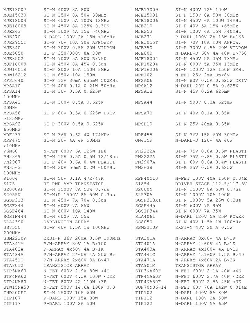
MJE13007 SI-N 400V 8A 80W | MJE13009 SI-N 400V 12A 100W MJE15030 SI-N 150V 8A 50W 30MHz | MJE15031 SI-P 150V 8A 50W 30MHz MJE18004 SI-N 450V 5A 100W 13MHz | MJE18006 SI-N 450V 6A 100W 14MHz MJE18008 SI-N 450V 8A 125W 0.3US | MJE210 SI-P 40V 5A 15W >65MHz MJE243 SI-N 100V 4A 15W >40MHz | MJE253 SI-P 100V 4A 15W >40MHz MJE270 N-DARL 100V 2A 15W >16MHz | MJE271 P-DARL 100V 2A 15W B>1K5 MJE2955T SI-P 70V 10A 90W AFPOWER | MJE3055T SI-N 70V 10A 90W AFPOW. MJE340 SI-N 300V 0.5A 20W VIDPOW | MJE350 SI-P 300V 0.5A 20W VIDPOW MJE5850 SI-P 350/300V 8A 80W | MJE800 N-DARL+D 60V 4A 40W B>750 MJE8502 SI-N 700V 5A 80W B>750 | MJF18004 SI-N 450V 5A 35W 13MHz MJF18008 SI-N 450V 8A 45W 0.3us | MJF18204 SI-N 600V 5A 35W 13MHz MJW16018 SI-P 800V 10A 150W 3MHz | MJW16206 SI-N 1200V 12A 150W 3MHz MJW16212 SI-N 650V 10A 150W | MPF102 N-FET 25V 2mA Up<8V MPS3640 SI-P 12V 80mA 635mW 500MHz | MPSA06 SI-N 80V 0.5A 0.625W DRIV MPSA10 SI-N 40V 0.1A 0.21W 50MHz | MPSA12 N-DARL 20V 0.5A 0.625W MPSA14 SI-N 30V 0.5A 0.625W | MPSA18 SI-N 45V 0.2A 625mW100MHz MPSA42 SI-N 300V 0.5A 0.625W | MPSA44 SI-N 500V 0.3A 625mW20MHz MPSA56 SI-P 80V 0.5A 0.625W DRIV | MPSA70 SI-P 40V 0.1A 0.35W>125MHz MPSA92 SI-P 300V 0.5A 0.625W | MPSH10 SI-N 25V 40mA 0.35W650MHz MRF237 SI-N 36V 0.6A 4W 174MHz | MRF455 SI-N 36V 15A 60W 30MHz MRF475 SI-N 20V 4A 4W 50MHz | ON4359 N-DARL+D 120V 4A 40W>10MHz P6N60 N-FET 600V 6A 125W 1E8 | PH2222A SI-N 75V 0.8A 0.5W PLASTI PH2369 SI-N 15V 0.5A 0.5W 12/18ns | PN2222A SI-N 75V 0.8A 0.5W PLASTI PN2907 SI-P 40V 0.6A 0.4W PLASTI | PN2907A SI-P 60V 0.6A 0.4W PLASTI PN3563 SI-N 30V 50mA 0.2W 600MHz | PN3638 SI-P 25V 0.5A 0.625W100MHz R1004 SI-N 50V 0.1A 47K/47K | RFP40N10 N-FET 100V 40A 160W 0.04E S175 RF PWR AMP TRANSIST0R | S1854 DRIVER STAGE 112.5/117.5V S2000AF SI-N 1500V 8A 50W 0.7us | S2000N SI-N 1500V 8A 50W 0.7us S2055N SI-N+D 1500V 8A 50W 0.3us | S2530A SI-N 1000V 10A 100W SGSF313 SI-N 450V 7A 70W 0.3us | SGSF313XI SI-N 1000V 5A 25W 0.3us SGSF344 SI-N 600V 7A 85W | SGSF445 SI-N 600V 7A 95W SGSF464 SI-N 600V 10A 140W | SGSIF344 SI-N 600V 7A 35W SGSIF444 SI-N 600V 7A 55W | SLA4061 N-DARL 120V 5A 25W POWER SLA4390 DARLINGTON ARRAY | SS8050 SI-N 40V 1.5A 1W 100MHz SS8550 SI-P 40V 1.5A 1W 100MHz | SSM2210P 2xSI-N 40V 20mA 0.5W200MHz SSM2220P 2xSI-P 36V 20mA 0.5W 190MHz | STA301A N-ARRAY 3x60V 4A B>1K STA341M P/N-ARRAY 30V 1A B>100 | STA401A N-ARRAY 4x60V 4A B>1K STA402A P-ARRAY 4x50V 4A B>1K | STA403A N-ARRAY 4x100V 4A B>1K STA434A P/N-ARRAY 2*60V 4A 20W B> | STA441C N-ARRAY 4x160V 1.5A B>40 STA451C P/N-ARRAY 2x60V 3A B>40 | STA471A N-ARRAY 4x60V 2A B>2K STA8012 TRANSISTOR ARRAY | STA901M TRANSISTOR ARRAY STP3NA60 N-FET 600V 2.9A 80W <4E | STP3NA60F N-FET 600V 2.1A 40W <4E STP4NA60 N-FET 600V 4.3A 100W <2E2 | STP4NA60F N-FET 600V 2.7A 40W <2E2 STP4NA80 N-FET 800V 4A 110W <3E | STP4NA80F N-FET 800V 2.5A 45W <3E STW15NA50 N-FET 500V 14.6A 190W 0.0 | SUP70N06-14 N-FET 60V 70A 142W 0.014E THD200FI SI-N 1500V 10A 60W | TIP102 N-DARL 100V 8A 80W TIP107 P-DARL 100V 15A 80W | TIP112 N-DARL 100V 2A 50W TIP117 P-DARL 100V 2A 50W | TIP122 N-DARL 100V 5A 65W
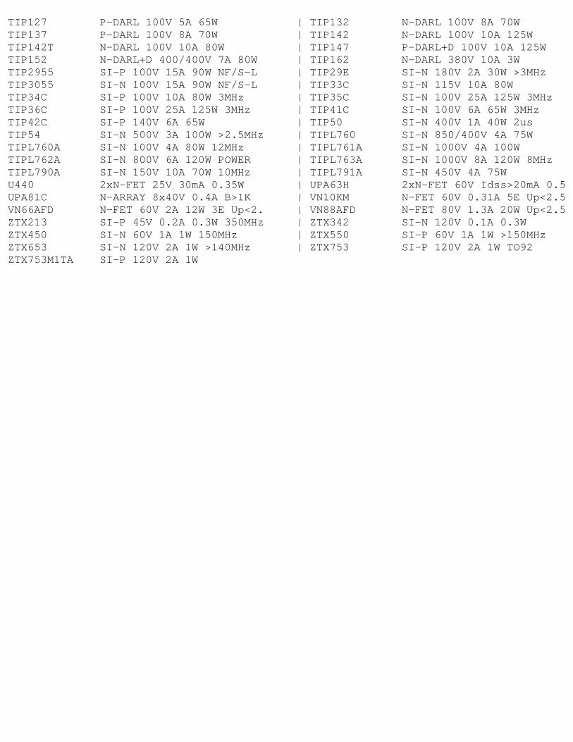
TIP127 P-DARL 100V 5A 65W | TIP132 N-DARL 100V 8A 70W TIP137 P-DARL 100V 8A 70W | TIP142 N-DARL 100V 10A 125W TIP142T N-DARL 100V 10A 80W | TIP147 P-DARL+D 100V 10A 125W TIP152 N-DARL+D 400/400V 7A 80W | TIP162 N-DARL 380V 10A 3W TIP2955 SI-P 100V 15A 90W NF/S-L | TIP29E SI-N 180V 2A 30W >3MHz TIP3055 SI-N 100V 15A 90W NF/S-L | TIP33C SI-N 115V 10A 80W TIP34C SI-P 100V 10A 80W 3MHz | TIP35C SI-N 100V 25A 125W 3MHz TIP36C SI-P 100V 25A 125W 3MHz | TIP41C SI-N 100V 6A 65W 3MHz TIP42C SI-P 140V 6A 65W | TIP50 SI-N 400V 1A 40W 2us TIP54 SI-N 500V 3A 100W >2.5MHz | TIPL760 SI-N 850/400V 4A 75W TIPL760A SI-N 100V 4A 80W 12MHz | TIPL761A SI-N 1000V 4A 100W TIPL762A SI-N 800V 6A 120W POWER | TIPL763A SI-N 1000V 8A 120W 8MHz TIPL790A SI-N 150V 10A 70W 10MHz | TIPL791A SI-N 450V 4A 75W U440 2xN-FET 25V 30mA 0.35W | UPA63H 2xN-FET 60V Idss>20mA 0.5 UPA81C N-ARRAY 8x40V 0.4A B>1K | VN10KM N-FET 60V 0.31A 5E Up<2.5 VN66AFD N-FET 60V 2A 12W 3E Up<2. | VN88AFD N-FET 80V 1.3A 20W Up<2.5 ZTX213 SI-P 45V 0.2A 0.3W 350MHz | ZTX342 SI-N 120V 0.1A 0.3W ZTX450 SI-N 60V 1A 1W 150MHz | ZTX550 SI-P 60V 1A 1W >150MHz ZTX653 SI-N 120V 2A 1W >140MHz | ZTX753 SI-P 120V 2A 1W TO92 ZTX753M1TA SI-P 120V 2A 1W
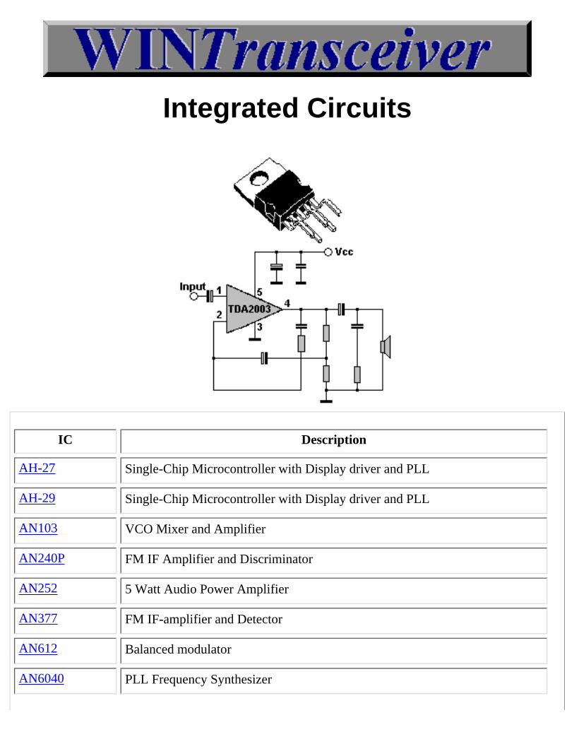
Integrated Circuits
IC Description
AH-27 Single-Chip Microcontroller with Display driver and PLL
AH-29 Single-Chip Microcontroller with Display driver and PLL
AN103 VCO Mixer and Amplifier
AN240P FM IF Amplifier and Discriminator
AN252 5 Watt Audio Power Amplifier
AN377 FM IF-amplifier and Detector
AN612 Balanced modulator
AN6040 PLL Frequency Synthesizer
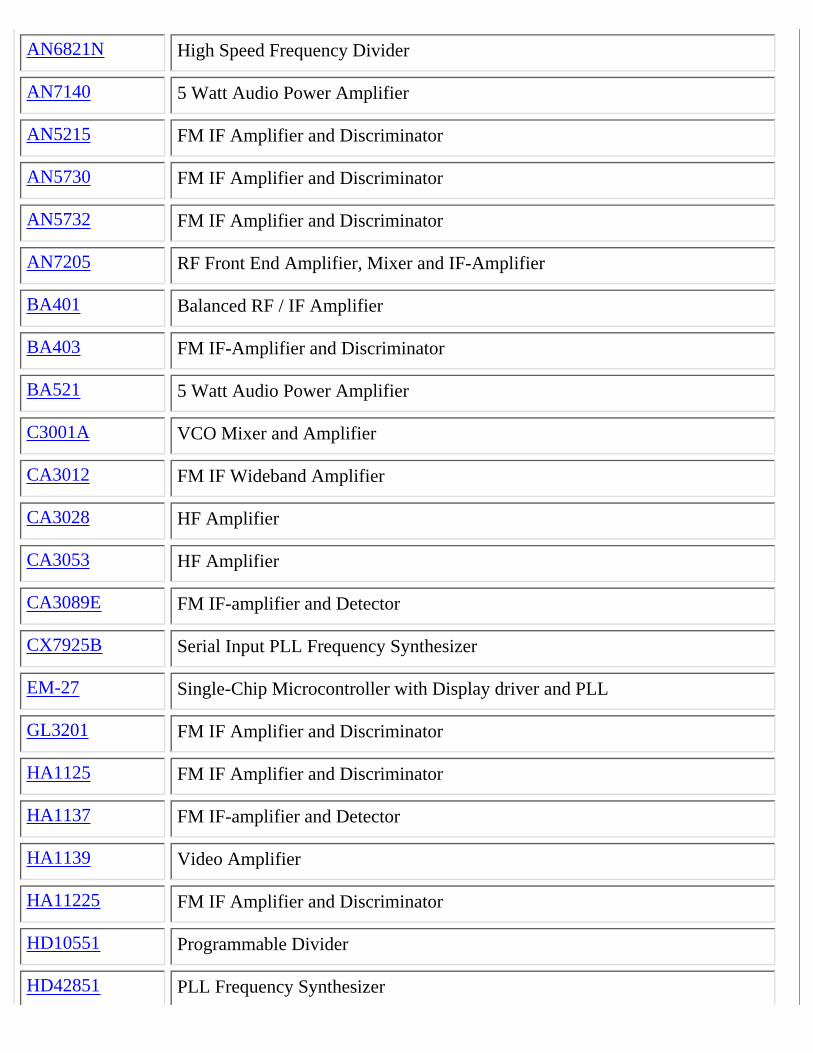
AN6821N High Speed Frequency Divider
AN7140 5 Watt Audio Power Amplifier
AN5215 FM IF Amplifier and Discriminator
AN5730 FM IF Amplifier and Discriminator
AN5732 FM IF Amplifier and Discriminator
AN7205 RF Front End Amplifier, Mixer and IF-Amplifier
BA401 Balanced RF / IF Amplifier
BA403 FM IF-Amplifier and Discriminator
BA521 5 Watt Audio Power Amplifier
C3001A VCO Mixer and Amplifier
CA3012 FM IF Wideband Amplifier
CA3028 HF Amplifier
CA3053 HF Amplifier
CA3089E FM IF-amplifier and Detector
CX7925B Serial Input PLL Frequency Synthesizer
EM-27 Single-Chip Microcontroller with Display driver and PLL
GL3201 FM IF Amplifier and Discriminator
HA1125 FM IF Amplifier and Discriminator
HA1137 FM IF-amplifier and Detector
HA1139 Video Amplifier
HA11225 FM IF Amplifier and Discriminator
HD10551 Programmable Divider
HD42851 PLL Frequency Synthesizer
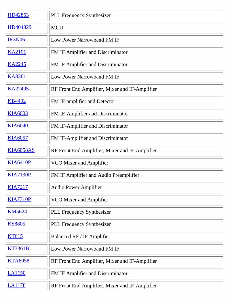
HD42853 PLL Frequency Synthesizer
HD404829 MCU
IR3N06 Low Power Narrowband FM IF
KA2101 FM IF Amplifier and Discriminator
KA2245 FM IF Amplifier and Discriminator
KA3361 Low Power Narrowband FM IF
KA22495 RF Front End Amplifier, Mixer and IF-Amplifier
KB4402 FM IF-amplifier and Detector
KIA6003 FM IF-Amplifier and Discriminator
KIA6040 FM IF-Amplifier and Discriminator
KIA6057 FM IF-Amplifier and Discriminator
KIA6058AS RF Front End Amplifier, Mixer and IF-Amplifier
KIA6410P VCO Mixer and Amplifier
KIA7130P FM IF Amplifier and Audio Preamplifier
KIA7217 Audio Power Amplifier
KIA7310P VCO Mixer and Amplifier
KM5624 PLL Frequency Synthesizer
KS8805 PLL Frequency Synthesizer
KT615 Balanced RF / IF Amplifier
KT3361B Low Power Narrowband FM IF
KTA6058 RF Front End Amplifier, Mixer and IF-Amplifier
LA1150 FM IF Amplifier and Discriminator
LA1178 RF Front End Amplifier, Mixer and IF-Amplifier
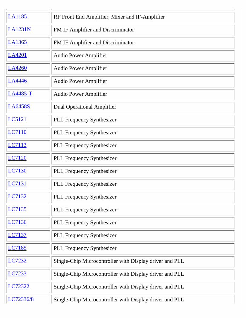
LA1185 RF Front End Amplifier, Mixer and IF-Amplifier
LA1231N FM IF Amplifier and Discriminator
LA1365 FM IF Amplifier and Discriminator
LA4201 Audio Power Amplifier
LA4260 Audio Power Amplifier
LA4446 Audio Power Amplifier
LA4485-T Audio Power Amplifier
LA6458S Dual Operational Amplifier
LC5121 PLL Frequency Synthesizer
LC7110 PLL Frequency Synthesizer
LC7113 PLL Frequency Synthesizer
LC7120 PLL Frequency Synthesizer
LC7130 PLL Frequency Synthesizer
LC7131 PLL Frequency Synthesizer
LC7132 PLL Frequency Synthesizer
LC7135 PLL Frequency Synthesizer
LC7136 PLL Frequency Synthesizer
LC7137 PLL Frequency Synthesizer
LC7185 PLL Frequency Synthesizer
LC7232 Single-Chip Microcontroller with Display driver and PLL
LC7233 Single-Chip Microcontroller with Display driver and PLL
LC72322 Single-Chip Microcontroller with Display driver and PLL
LC72336/8 Single-Chip Microcontroller with Display driver and PLL
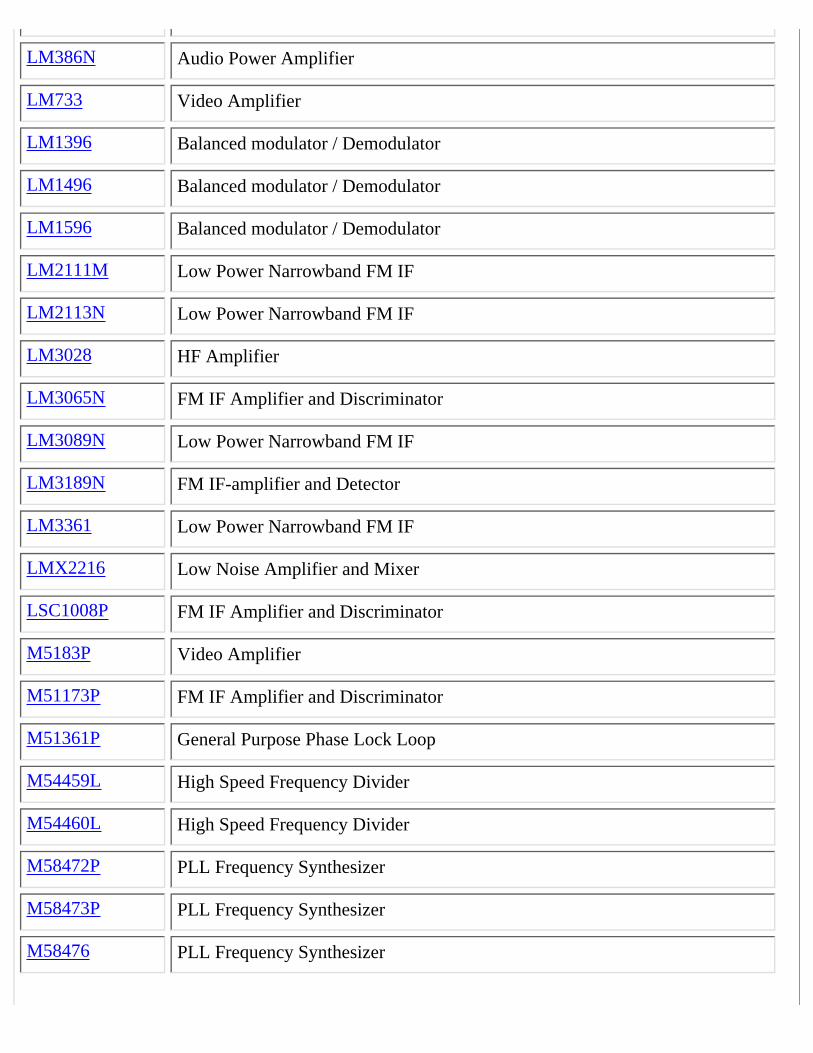
LM386N Audio Power Amplifier
LM733 Video Amplifier
LM1396 Balanced modulator / Demodulator
LM1496 Balanced modulator / Demodulator
LM1596 Balanced modulator / Demodulator
LM2111M Low Power Narrowband FM IF
LM2113N Low Power Narrowband FM IF
LM3028 HF Amplifier
LM3065N FM IF Amplifier and Discriminator
LM3089N Low Power Narrowband FM IF
LM3189N FM IF-amplifier and Detector
LM3361 Low Power Narrowband FM IF
LMX2216 Low Noise Amplifier and Mixer
LSC1008P FM IF Amplifier and Discriminator
M5183P Video Amplifier
M51173P FM IF Amplifier and Discriminator
M51361P General Purpose Phase Lock Loop
M54459L High Speed Frequency Divider
M54460L High Speed Frequency Divider
M58472P PLL Frequency Synthesizer
M58473P PLL Frequency Synthesizer
M58476 PLL Frequency Synthesizer
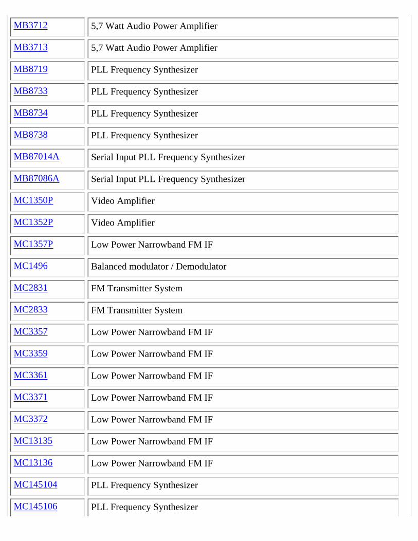
MB3712 5,7 Watt Audio Power Amplifier
MB3713 5,7 Watt Audio Power Amplifier
MB8719 PLL Frequency Synthesizer
MB8733 PLL Frequency Synthesizer
MB8734 PLL Frequency Synthesizer
MB8738 PLL Frequency Synthesizer
MB87014A Serial Input PLL Frequency Synthesizer
MB87086A Serial Input PLL Frequency Synthesizer
MC1350P Video Amplifier
MC1352P Video Amplifier
MC1357P Low Power Narrowband FM IF
MC1496 Balanced modulator / Demodulator
MC2831 FM Transmitter System
MC2833 FM Transmitter System
MC3357 Low Power Narrowband FM IF
MC3359 Low Power Narrowband FM IF
MC3361 Low Power Narrowband FM IF
MC3371 Low Power Narrowband FM IF
MC3372 Low Power Narrowband FM IF
MC13135 Low Power Narrowband FM IF
MC13136 Low Power Narrowband FM IF
MC145104 PLL Frequency Synthesizer
MC145106 PLL Frequency Synthesizer
MC145107 PLL Frequency Synthesizer
MC145109 PLL Frequency Synthesizer
MC145151 PLL Frequency Synthesizer
MC145152 PLL Frequency Synthesizer
MC145155 PLL Frequency Synthesizer
MC145156 PLL Frequency Synthesizer
MC145157 PLL Frequency Synthesizer
MC145158 PLL Frequency Synthesizer
MC145163 PLL Frequency Synthesizer
MM48141 PLL Frequency Synthesizer
MM55104 PLL Frequency Synthesizer
MM55106 PLL Frequency Synthesizer
MM55107 PLL Frequency Synthesizer
MM55108 PLL Frequency Synthesizer
MM55116 PLL Frequency Synthesizer
MM55126 PLL Frequency Synthesizer
MN6040 PLL Frequency Synthesizer
MN6040A PLL Frequency Synthesizer
MSC42502P PLL Frequency Synthesizer
MSM5807 PLL Frequency Synthesizer
MSM5907 PLL Frequency Synthesizer
MWA110 Wide-Band RF Amplifier
MWA120 Wide-Band RF Amplifier
MWA130 Wide-Band RF Amplifier
N5596 Balanced modulator / Demodulator
NDC40013 PLL Frequency Synthesizer
NE565N General Purpose Phase Lock Loop
NE592 Video Amplifier
NE602 Double-balanced mixer and oscillator
NE605 FM IF Amplifier and Discriminator
NE606 FM IF Amplifier and Discriminator
NE612 Double-balanced mixer and oscillator
NE616 FM IF Amplifier and Discriminator
NJM386N Audio Power Amplifier
NJM386S Audio Power Amplifier
NJM1496 Balanced modulator / Demodulator
NJM2203 Double-balanced mixer and oscillator
NJM2206 FM IF-Amplifier and Discriminator
NJM2902N Quad Operational Amplifier
NJM3357 Low Power Narrowband FM IF
NJM3359 Low Power Narrowband FM IF
NJM4558 Dual Operational Amplifier
NJM4558S Dual Operational Amplifier
PLL02A PLL Frequency Synthesizer
PLL03A PLL Frequency Synthesizer
PLL0305A Serial Input PLL Frequency Synthesizer
PLL08A PLL Frequency Synthesizer
PLL2002A Serial Input PLL Frequency Synthesizer
RCI8719 PLL Frequency Synthesizer
RCL10483 Narrowband FM/AM IF-amplifier and Demodulator
REC86345 PLL Frequency Synthesizer
REN1165 5 Watt Audio Power Amplifier
RL7320 Balanced Modulator / Demodulator
SA602A Double-balanced mixer and oscillator
SA604A Low Power Narrowband FM IF
SA612A Double-balanced mixer and oscillator
SC70231P Video Amplifier
SK1166 5 Watt Audio Power Amplifier
SK3225 Balanced RF / IF Amplifier
SK3445 VCO Mixer and Amplifier
SK3487 FM IF Amplifier and Discriminator
SK3827 5 Watt Audio Power Amplifier
SK7799 Audio Power Amplifier
SM5104 PLL Frequency Synthesizer
SM5107 PLL Frequency Synthesizer
SM5109 PLL Frequency Synthesizer
SM5118 PLL Frequency Synthesizer
SM5123A PLL Frequency Synthesizer

SM5124A PLL Frequency Synthesizer
SM5152A Serial Input PLL Frequency Synthesizer
SM5158A PLL Frequency Synthesizer
SN76514 Balanced modulator / Demodulator
SN76600P Video Amplifier
SN76642N Low Power Narrowband FM IF
SN76650P Video Amplifier
SN76643N Low Power Narrowband FM IF
SN76664N FM IF Amplifier and Discriminator
SO42P Duble Balanced Modulator / Demodulator
STK4241 Audio Power Amplifier
SY-105 Single-Chip Microcontroller with Display driver and PLL
SY-202 Single-Chip Microcontroller with Display driver and PLL
SY-203 Single-Chip Microcontroller with Display driver and PLL
SY-204 Single-Chip Microcontroller with Display driver and PLL
SY-501 Single-Chip Microcontroller with Display driver and PLL
TA7045 HF Amplifier
TA7130 FM IF Amplifier and Discriminator
TA7176P FM IF Amplifier and Discriminator
TA7200 Audio Power Amplifier
TA7204 Audio Power Amplifier
TA7205P Audio Power Amplifier
TA7217AP Audio Power Amplifier
TA7222 Audio Power Amplifier
TA7303P FM IF Amplifier and Discriminator
TA7310P VCO Mixer and Amplifier
TA7320P Balanced Modulator / Demodulator
TA7358AP RF Front End Amplifier, Mixer and IF-Amplifier
TA7368 Audio Power Amplifier
TA75557 Dual Operational Amplifier
TA75558 Dual Operational Amplifier
TC5080P Programmable Divider
TC5081P PLL Phase-Locked-Loop
TC5082P Oscillator and Reference Divider
TC9100P PLL Frequency Synthesizer
TC9102 PLL Frequency Synthesizer
TC9103 PLL Frequency Synthesizer
TC9106 PLL Frequency Synthesizer
TC9109 PLL Frequency Synthesizer
TC9119 PLL Frequency Synthesizer
TC9122P Programmable Divider
TCA3189 FM IF-amplifier and Detector
TDA1200 FM IF-amplifier and Detector
TDA1352 Video Amplifier
TDA1905 Audio Power Amplifier
TDA2003 Audio Power Amplifier
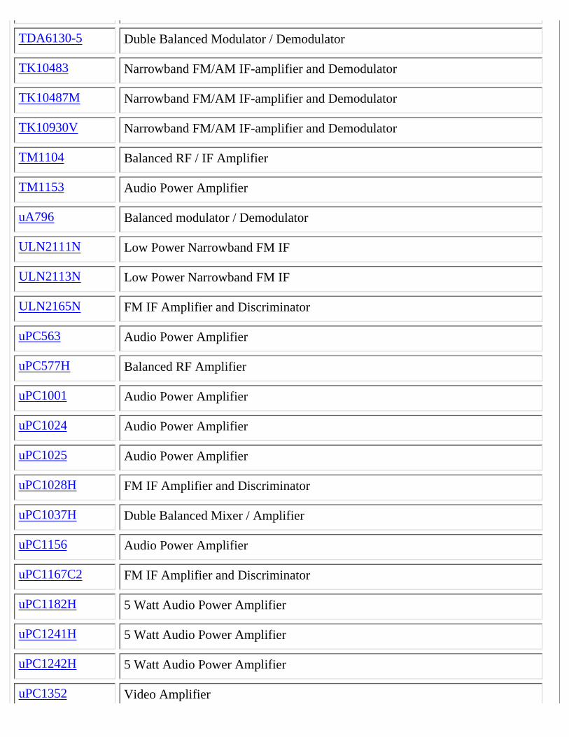
TDA6130-5 Duble Balanced Modulator / Demodulator
TK10483 Narrowband FM/AM IF-amplifier and Demodulator
TK10487M Narrowband FM/AM IF-amplifier and Demodulator
TK10930V Narrowband FM/AM IF-amplifier and Demodulator
TM1104 Balanced RF / IF Amplifier
TM1153 Audio Power Amplifier
uA796 Balanced modulator / Demodulator
ULN2111N Low Power Narrowband FM IF
ULN2113N Low Power Narrowband FM IF
ULN2165N FM IF Amplifier and Discriminator
uPC563 Audio Power Amplifier
uPC577H Balanced RF Amplifier
uPC1001 Audio Power Amplifier
uPC1024 Audio Power Amplifier
uPC1025 Audio Power Amplifier
uPC1028H FM IF Amplifier and Discriminator
uPC1037H Duble Balanced Mixer / Amplifier
uPC1156 Audio Power Amplifier
uPC1167C2 FM IF Amplifier and Discriminator
uPC1182H 5 Watt Audio Power Amplifier
uPC1241H 5 Watt Audio Power Amplifier
uPC1242H 5 Watt Audio Power Amplifier
uPC1352 Video Amplifier
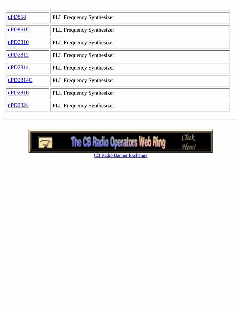
uPD858 PLL Frequency Synthesizer
uPD861C PLL Frequency Synthesizer
uPD2810 PLL Frequency Synthesizer
uPD2812 PLL Frequency Synthesizer
uPD2814 PLL Frequency Synthesizer
uPD2814C PLL Frequency Synthesizer
uPD2816 PLL Frequency Synthesizer
uPD2824 PLL Frequency Synthesizer
CB Radio Banner Exchange
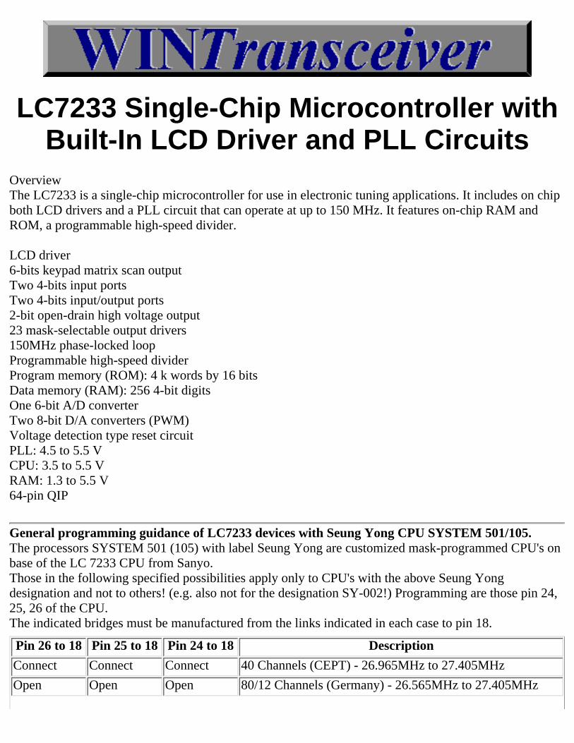
LC7233 Single-Chip Microcontroller withBuilt-In LCD Driver and PLL Circuits
OverviewThe LC7233 is a single-chip microcontroller for use in electronic tuning applications. It includes on chipboth LCD drivers and a PLL circuit that can operate at up to 150 MHz. It features on-chip RAM andROM, a programmable high-speed divider.
LCD driver6-bits keypad matrix scan outputTwo 4-bits input portsTwo 4-bits input/output ports2-bit open-drain high voltage output23 mask-selectable output drivers150MHz phase-locked loopProgrammable high-speed dividerProgram memory (ROM): 4 k words by 16 bitsData memory (RAM): 256 4-bit digitsOne 6-bit A/D converterTwo 8-bit D/A converters (PWM)Voltage detection type reset circuitPLL: 4.5 to 5.5 VCPU: 3.5 to 5.5 VRAM: 1.3 to 5.5 V64-pin QIP
General programming guidance of LC7233 devices with Seung Yong CPU SYSTEM 501/105.The processors SYSTEM 501 (105) with label Seung Yong are customized mask-programmed CPU's onbase of the LC 7233 CPU from Sanyo.Those in the following specified possibilities apply only to CPU's with the above Seung Yongdesignation and not to others! (e.g. also not for the designation SY-002!) Programming are those pin 24,25, 26 of the CPU.The indicated bridges must be manufactured from the links indicated in each case to pin 18.
Pin 26 to 18 Pin 25 to 18 Pin 24 to 18 Description
Connect Connect Connect 40 Channels (CEPT) - 26.965MHz to 27.405MHz
Open Open Open 80/12 Channels (Germany) - 26.565MHz to 27.405MHz
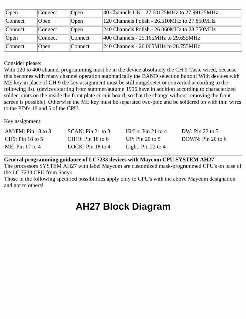
Open Connect Open 40 Channels UK - 27.60125MHz to 27.99125MHz
Connect Open Open 120 Channels Polish - 26.510MHz to 27.850MHz
Connect Connect Open 240 Channels Polish - 26.060MHz to 28.750MHz
Open Connect Connect 400 Channels - 25.165MHz to 29.655MHz
Connect Open Connect 240 Channels - 26.065MHz to 28.755MHz
Consider please:With 120 to 400 channel programming must be in the device absolutely the CH 9-Taste wired, becausethis becomes with many channel operation automatically the BAND selection button! With devices withME key in place of CH 9 the key assignment must be still umgeloetet or converted according to thefollowing list. (devices starting from summer/autumn 1996 have in addition according to characterizedsolder joints on the inside the front plate circuit board, so that the change without removing the frontscreen is possible). Otherwise the ME key must be separated two-pole and be soldered on with thin wiresto the PIN's 18 and 5 of the CPU.
Key assignment:
AM/FM: Pin 18 to 3 SCAN: Pin 21 to 3 Hi/Lo: Pin 21 to 4 DW: Pin 22 to 5CH9: Pin 18 to 5 CH19: Pin 18 to 6 UP: Pin 20 to 5 DOWN: Pin 20 to 6ME: Pin 17 to 4 LOCK: Pin 18 to 4 Light: Pin 22 to 4
General programming guidance of LC7233 devices with Maycom CPU SYSTEM AH27The processors SYSTEM AH27 with label Maycom are customized mask-programmed CPU's on base ofthe LC 7233 CPU from Sanyo.Those in the following specified possibilities apply only to CPU's with the above Maycom designationand not to others!
AH27 Block Diagram
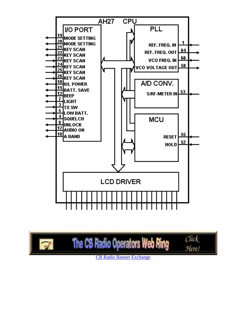
CB Radio Banner Exchange
LC72336 / LC72338 Single-ChipMicrocontrollers with Built-In LCD Driver
and PLL Circuits
OverviewThe LC72336 and LC72338 are single-chip microcontrollers for use in electronic tuners. These productsinclude on chip a PLL circuit that can operate at up to 150 MHz and 1/3 duty LCD drivers. They featurea highly efficient instruction set and powerful hardware.
FunctionsHigh-speed programmable dividerProgram memory (ROM)— LC72336: 6143 ´ 16 bits (12 kB)— LC72338: 8191 ´ 16 bits (16 kB)Data memory (RAM): 512 ´ 4 bitsAll instructions are one-word instructionsCycle time: 1.33 µsStack: 8 levelsLCD drivers: Up to 96 segments (1/3 duty, 1/3 bias)Serial I/O: Up to 3 channels (8-bit 3-wire type)External interrupts: 2 interrupts (INT0, INT1) Interrupt on rising or falling edge (selectable)Internal interrupts: 3 interrupt Two built-in timer interrupts and 1 serial I/O interruptNested interrupt levels: 4 levelsD/A converter: 4 channels (8-bit PWM output)A/D converter: 4 channels(6-bit successive approximation) • General-purpose ports:— Input ports: 8— Output ports: 12 (16 maximum)— I/O ports: 8 (20 maximum, can be switched between input and output in bit units.)PLL block: Supports 4 types of dead zone control, and includes a built-in unlock detection circuit.Supports 12 different reference frequencies.Universal counter: 20 bits (Can be used for either frequency or period measurement.)Timers: Eight types of time measurementBeep function: Six beep tonesReset: Built-in voltage detection type reset circuitHalt mode: Stops the controller operating clock.
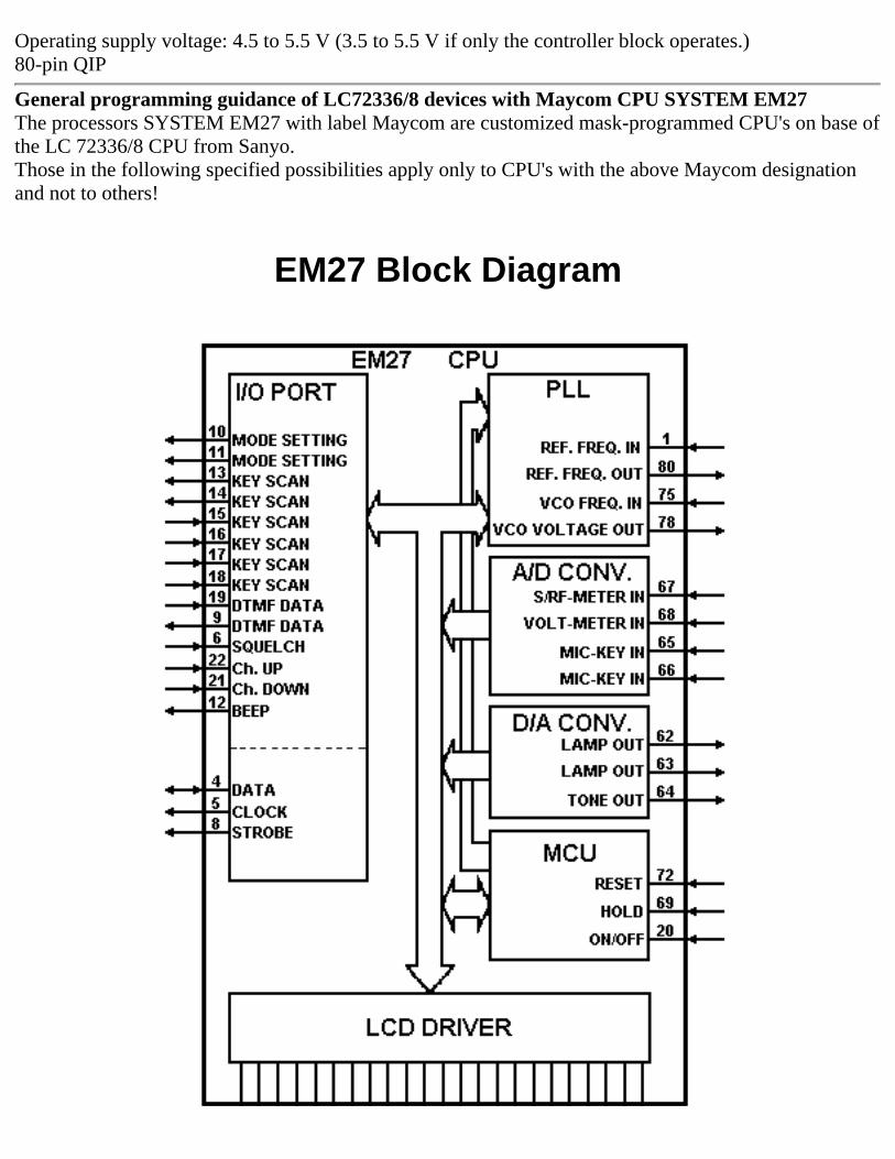
Operating supply voltage: 4.5 to 5.5 V (3.5 to 5.5 V if only the controller block operates.)80-pin QIP
General programming guidance of LC72336/8 devices with Maycom CPU SYSTEM EM27The processors SYSTEM EM27 with label Maycom are customized mask-programmed CPU's on base ofthe LC 72336/8 CPU from Sanyo.Those in the following specified possibilities apply only to CPU's with the above Maycom designationand not to others!
EM27 Block Diagram
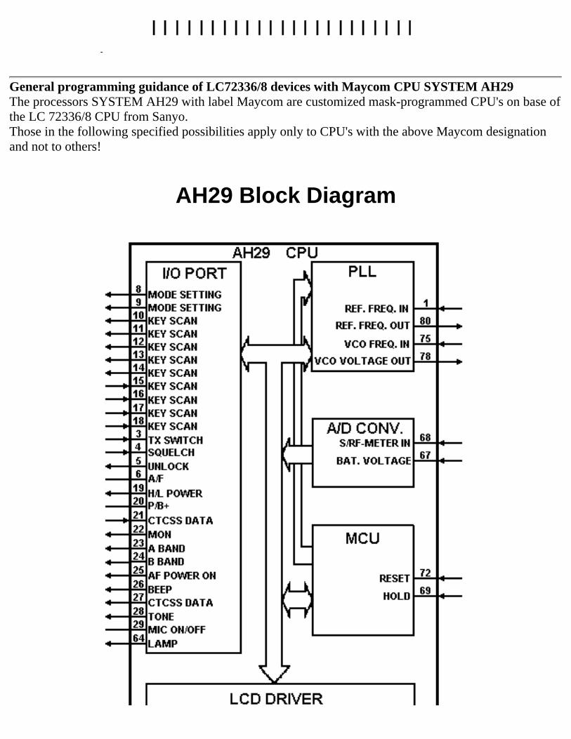
General programming guidance of LC72336/8 devices with Maycom CPU SYSTEM AH29The processors SYSTEM AH29 with label Maycom are customized mask-programmed CPU's on base ofthe LC 72336/8 CPU from Sanyo.Those in the following specified possibilities apply only to CPU's with the above Maycom designationand not to others!
AH29 Block Diagram

CB Radio Banner Exchange
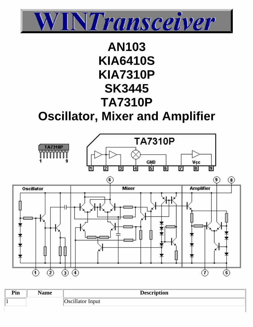
AN103KIA6410SKIA7310PSK3445
TA7310POscillator, Mixer and Amplifier
Pin Name Description
1 Oscillator Input
2 Oscillator Output
3 Oscillator Output - Buffered
4 Mixer Input
5 GND Ground
6 Mixer Output
7 Amplifier Input
8 Vcc Positive Supply Voltage - 9 Volt
9 Amplifier Output
CB Radio Banner Exchange
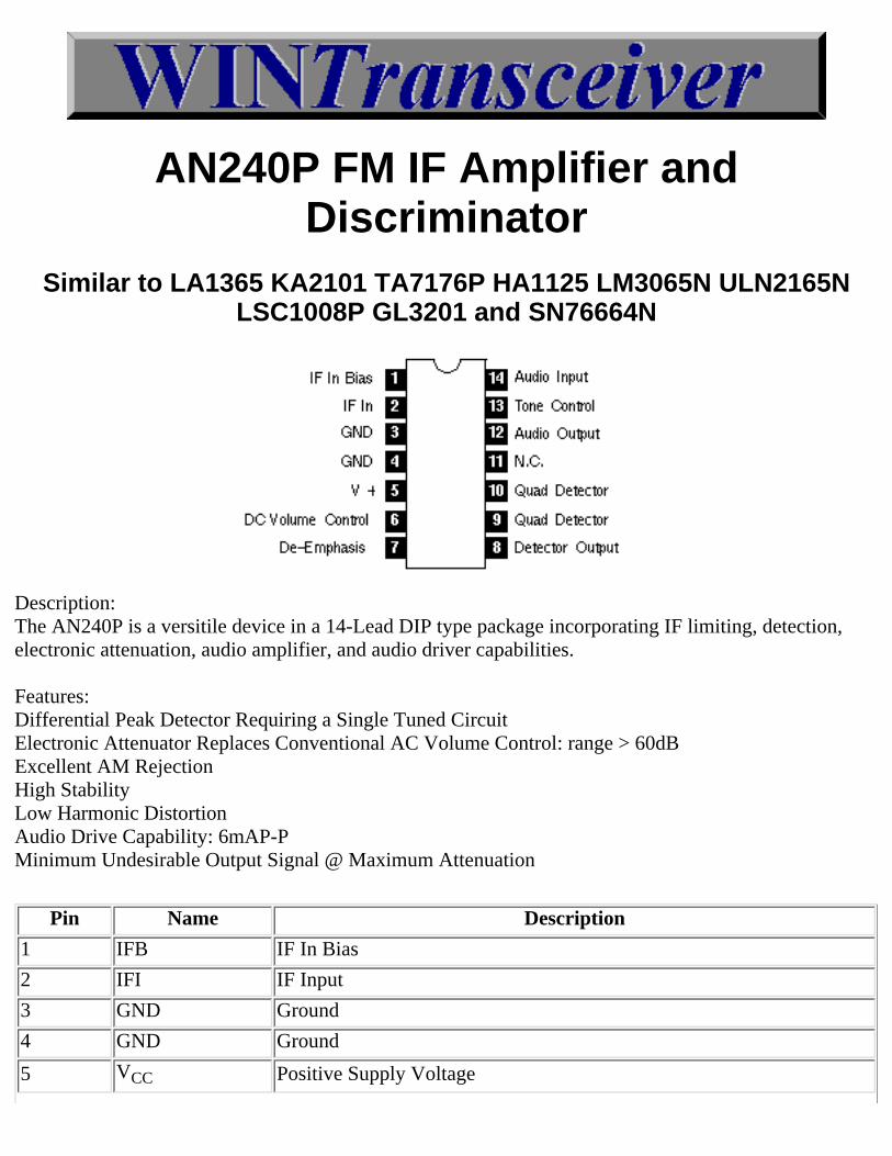
AN240P FM IF Amplifier andDiscriminator
Similar to LA1365 KA2101 TA7176P HA1125 LM3065N ULN2165NLSC1008P GL3201 and SN76664N
Description:The AN240P is a versitile device in a 14-Lead DIP type package incorporating IF limiting, detection,electronic attenuation, audio amplifier, and audio driver capabilities.
Features:Differential Peak Detector Requiring a Single Tuned CircuitElectronic Attenuator Replaces Conventional AC Volume Control: range > 60dBExcellent AM RejectionHigh StabilityLow Harmonic DistortionAudio Drive Capability: 6mAP-PMinimum Undesirable Output Signal @ Maximum Attenuation
Pin Name Description
1 IFB IF In Bias
2 IFI IF Input
3 GND Ground
4 GND Ground
5 VCC Positive Supply Voltage
6 DC DC Volume Control
7 DE De-Emphasis
8 DO Detector Output
9 QD Quad Detector
10 QD Quad detector
11 NC No Connection
12 AO Audio Output
13 TC Tone Control
14 AI Audio Input
CB Radio Banner Exchange
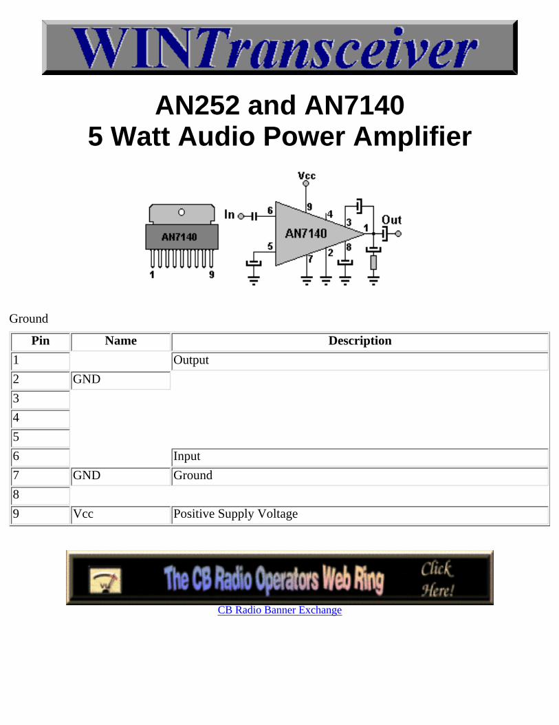
AN252 and AN71405 Watt Audio Power Amplifier
Ground
Pin Name Description
1 Output
2 GND
3
4
5
6 Input
7 GND Ground
8
9 Vcc Positive Supply Voltage
CB Radio Banner Exchange
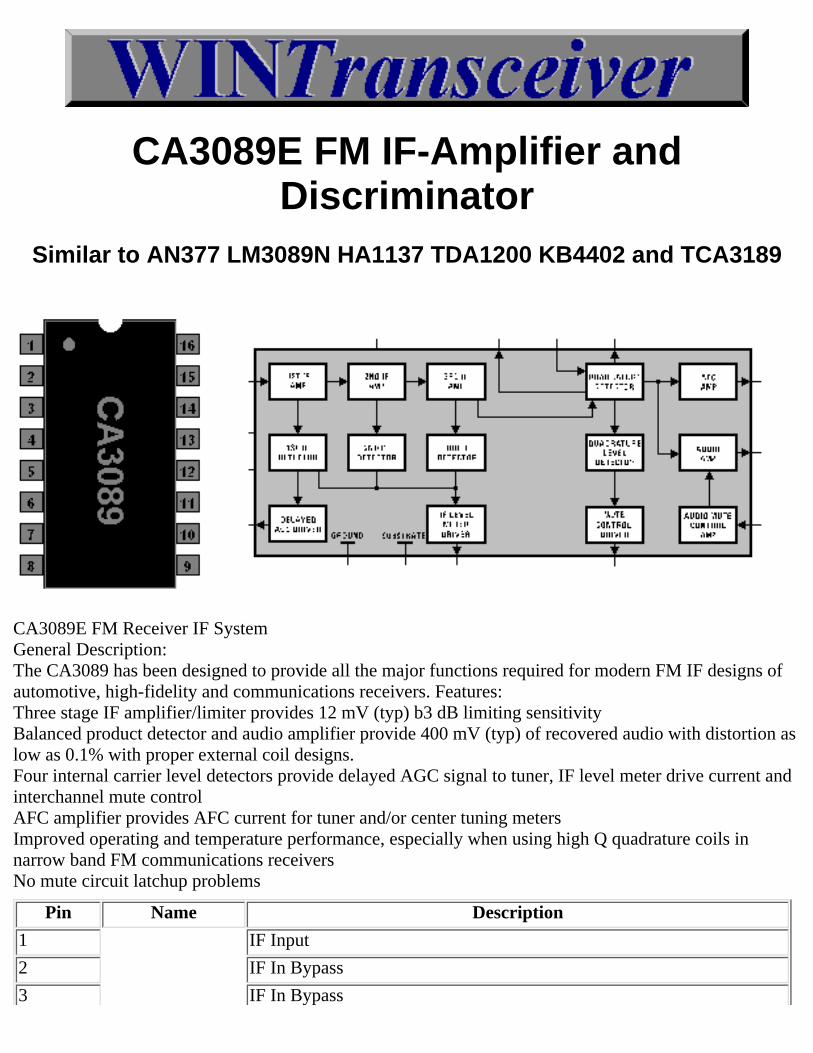
CA3089E FM IF-Amplifier andDiscriminator
Similar to AN377 LM3089N HA1137 TDA1200 KB4402 and TCA3189
CA3089E FM Receiver IF SystemGeneral Description:The CA3089 has been designed to provide all the major functions required for modern FM IF designs ofautomotive, high-fidelity and communications receivers. Features:Three stage IF amplifier/limiter provides 12 mV (typ) b3 dB limiting sensitivityBalanced product detector and audio amplifier provide 400 mV (typ) of recovered audio with distortion aslow as 0.1% with proper external coil designs.Four internal carrier level detectors provide delayed AGC signal to tuner, IF level meter drive current andinterchannel mute controlAFC amplifier provides AFC current for tuner and/or center tuning metersImproved operating and temperature performance, especially when using high Q quadrature coils innarrow band FM communications receiversNo mute circuit latchup problems
Pin Name Description
1 IF Input
2 IF In Bypass
3 IF In Bypass
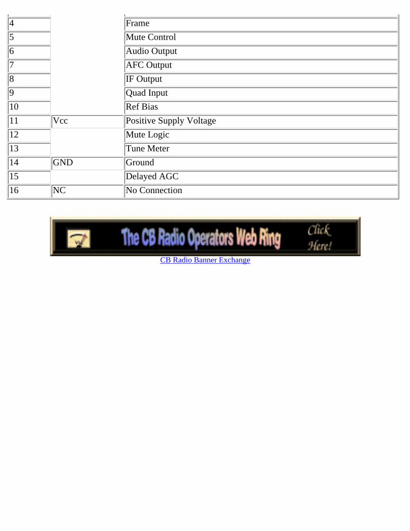
4 Frame
5 Mute Control
6 Audio Output
7 AFC Output
8 IF Output
9 Quad Input
10 Ref Bias
11 Vcc Positive Supply Voltage
12 Mute Logic
13 Tune Meter
14 GND Ground
15 Delayed AGC
16 NC No Connection
CB Radio Banner Exchange
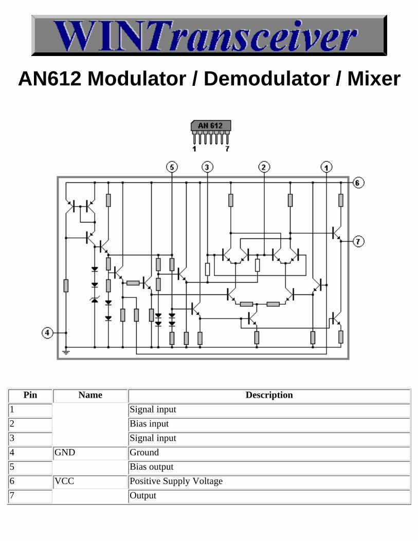
AN612 Modulator / Demodulator / Mixer
Pin Name Description
1 Signal input
2 Bias input
3 Signal input
4 GND Ground
5 Bias output
6 VCC Positive Supply Voltage
7 Output

CB Radio Banner Exchange
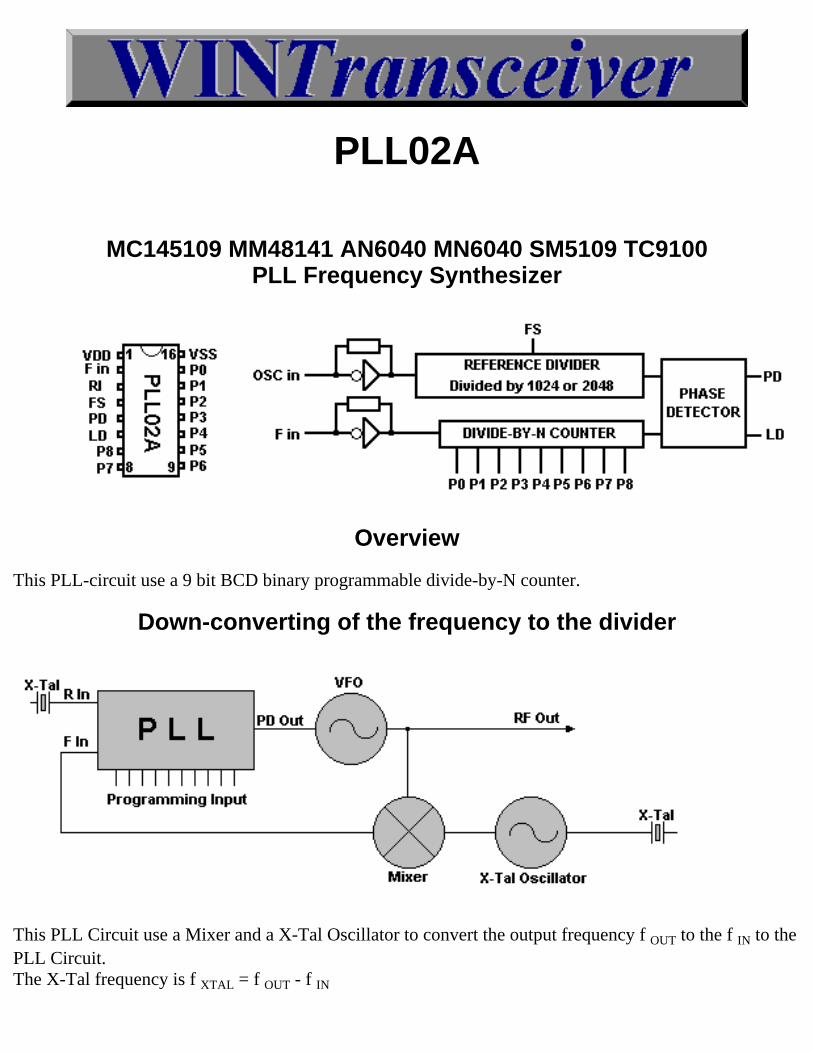
PLL02A
MC145109 MM48141 AN6040 MN6040 SM5109 TC9100PLL Frequency Synthesizer
Overview
This PLL-circuit use a 9 bit BCD binary programmable divide-by-N counter.
Down-converting of the frequency to the divider
This PLL Circuit use a Mixer and a X-Tal Oscillator to convert the output frequency f OUT to the f IN to thePLL Circuit.The X-Tal frequency is f XTAL = f OUT - f IN
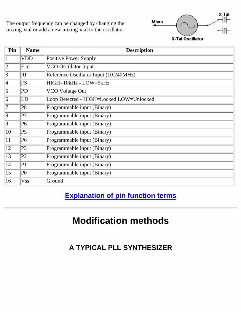
The output frequency can be changed by changing themixing-xtal or add a new mixing-xtal to the oscillator.
Pin Name Description
1 VDD Positive Power Supply
2 F in VCO Oscillator Input
3 RI Reference Oscillator Input (10.240MHz)
4 FS HIGH=10kHz - LOW=5kHz
5 PD VCO Voltage Out
6 LD Loop Detected - HIGH=Locked LOW=Unlocked
7 P8 Programmable input (Binary)
8 P7 Programmable input (Binary)
9 P6 Programmable input (Binary)
10 P5 Programmable input (Binary)
11 P6 Programmable input (Binary)
12 P3 Programmable input (Binary)
13 P2 Programmable input (Binary)
14 P1 Programmable input (Binary)
15 P0 Programmable input (Binary)
16 Vss Ground
Explanation of pin function terms
Modification methods
A TYPICAL PLL SYNTHESIZER
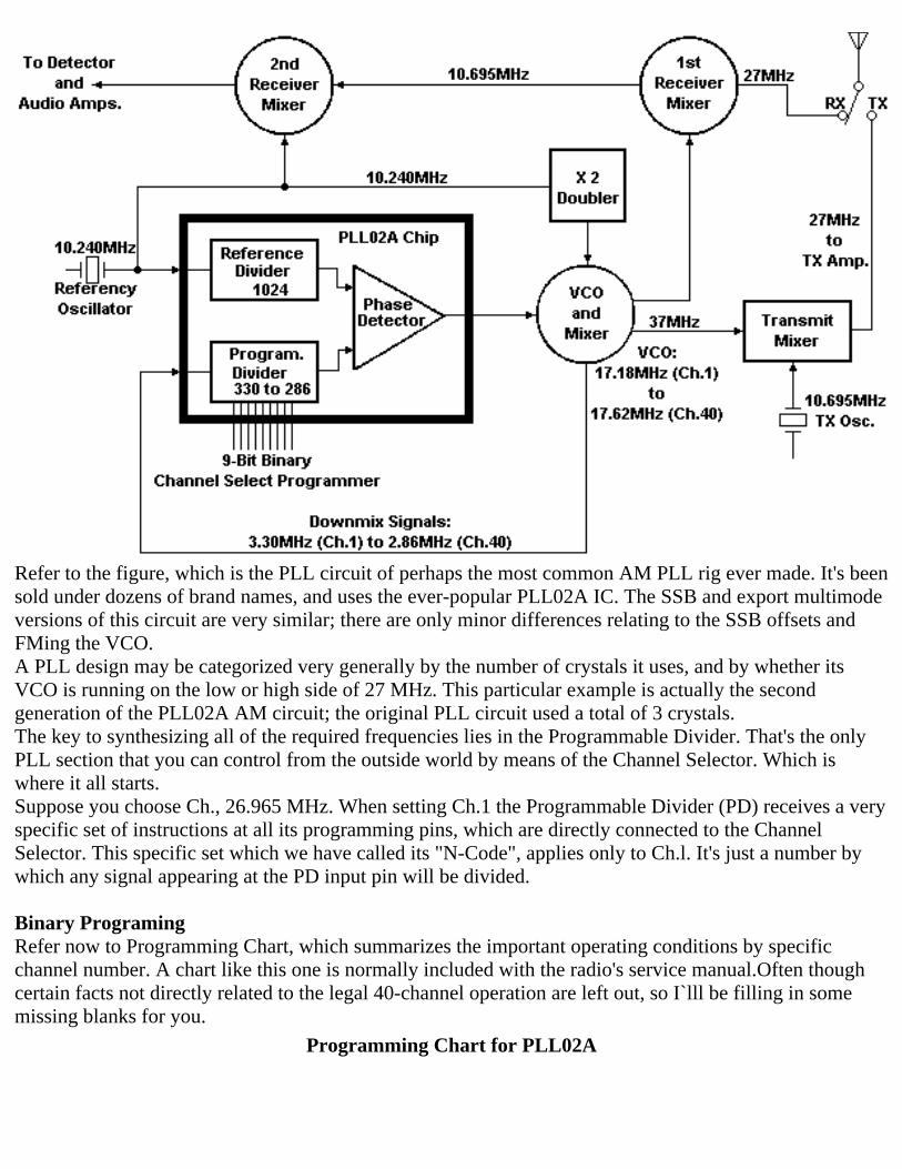
Refer to the figure, which is the PLL circuit of perhaps the most common AM PLL rig ever made. It's beensold under dozens of brand names, and uses the ever-popular PLL02A IC. The SSB and export multimodeversions of this circuit are very similar; there are only minor differences relating to the SSB offsets andFMing the VCO.A PLL design may be categorized very generally by the number of crystals it uses, and by whether itsVCO is running on the low or high side of 27 MHz. This particular example is actually the secondgeneration of the PLL02A AM circuit; the original PLL circuit used a total of 3 crystals.The key to synthesizing all of the required frequencies lies in the Programmable Divider. That's the onlyPLL section that you can control from the outside world by means of the Channel Selector. Which iswhere it all starts.Suppose you choose Ch., 26.965 MHz. When setting Ch.1 the Programmable Divider (PD) receives a veryspecific set of instructions at all its programming pins, which are directly connected to the ChannelSelector. This specific set which we have called its "N-Code", applies only to Ch.l. It's just a number bywhich any signal appearing at the PD input pin will be divided.
Binary ProgramingRefer now to Programming Chart, which summarizes the important operating conditions by specificchannel number. A chart like this one is normally included with the radio's service manual.Often thoughcertain facts not directly related to the legal 40-channel operation are left out, so I`lll be filling in somemissing blanks for you.
Programming Chart for PLL02A
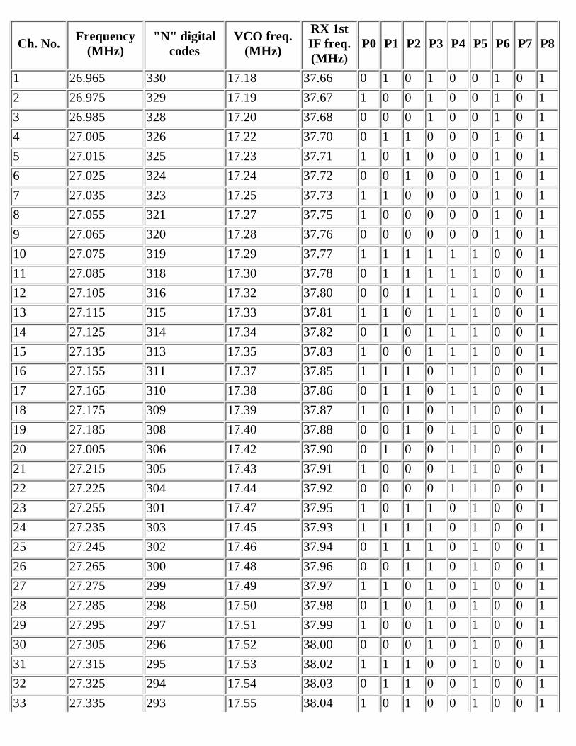
Ch. No. Frequency(MHz)
"N" digitalcodes
VCO freq.(MHz)
RX 1stIF freq.(MHz)
P0 P1 P2 P3 P4 P5 P6 P7 P8
1 26.965 330 17.18 37.66 0 1 0 1 0 0 1 0 1
2 26.975 329 17.19 37.67 1 0 0 1 0 0 1 0 1
3 26.985 328 17.20 37.68 0 0 0 1 0 0 1 0 1
4 27.005 326 17.22 37.70 0 1 1 0 0 0 1 0 1
5 27.015 325 17.23 37.71 1 0 1 0 0 0 1 0 1
6 27.025 324 17.24 37.72 0 0 1 0 0 0 1 0 1
7 27.035 323 17.25 37.73 1 1 0 0 0 0 1 0 1
8 27.055 321 17.27 37.75 1 0 0 0 0 0 1 0 1
9 27.065 320 17.28 37.76 0 0 0 0 0 0 1 0 1
10 27.075 319 17.29 37.77 1 1 1 1 1 1 0 0 1
11 27.085 318 17.30 37.78 0 1 1 1 1 1 0 0 1
12 27.105 316 17.32 37.80 0 0 1 1 1 1 0 0 1
13 27.115 315 17.33 37.81 1 1 0 1 1 1 0 0 1
14 27.125 314 17.34 37.82 0 1 0 1 1 1 0 0 1
15 27.135 313 17.35 37.83 1 0 0 1 1 1 0 0 1
16 27.155 311 17.37 37.85 1 1 1 0 1 1 0 0 1
17 27.165 310 17.38 37.86 0 1 1 0 1 1 0 0 1
18 27.175 309 17.39 37.87 1 0 1 0 1 1 0 0 1
19 27.185 308 17.40 37.88 0 0 1 0 1 1 0 0 1
20 27.005 306 17.42 37.90 0 1 0 0 1 1 0 0 1
21 27.215 305 17.43 37.91 1 0 0 0 1 1 0 0 1
22 27.225 304 17.44 37.92 0 0 0 0 1 1 0 0 1
23 27.255 301 17.47 37.95 1 0 1 1 0 1 0 0 1
24 27.235 303 17.45 37.93 1 1 1 1 0 1 0 0 1
25 27.245 302 17.46 37.94 0 1 1 1 0 1 0 0 1
26 27.265 300 17.48 37.96 0 0 1 1 0 1 0 0 1
27 27.275 299 17.49 37.97 1 1 0 1 0 1 0 0 1
28 27.285 298 17.50 37.98 0 1 0 1 0 1 0 0 1
29 27.295 297 17.51 37.99 1 0 0 1 0 1 0 0 1
30 27.305 296 17.52 38.00 0 0 0 1 0 1 0 0 1
31 27.315 295 17.53 38.02 1 1 1 0 0 1 0 0 1
32 27.325 294 17.54 38.03 0 1 1 0 0 1 0 0 1
33 27.335 293 17.55 38.04 1 0 1 0 0 1 0 0 1
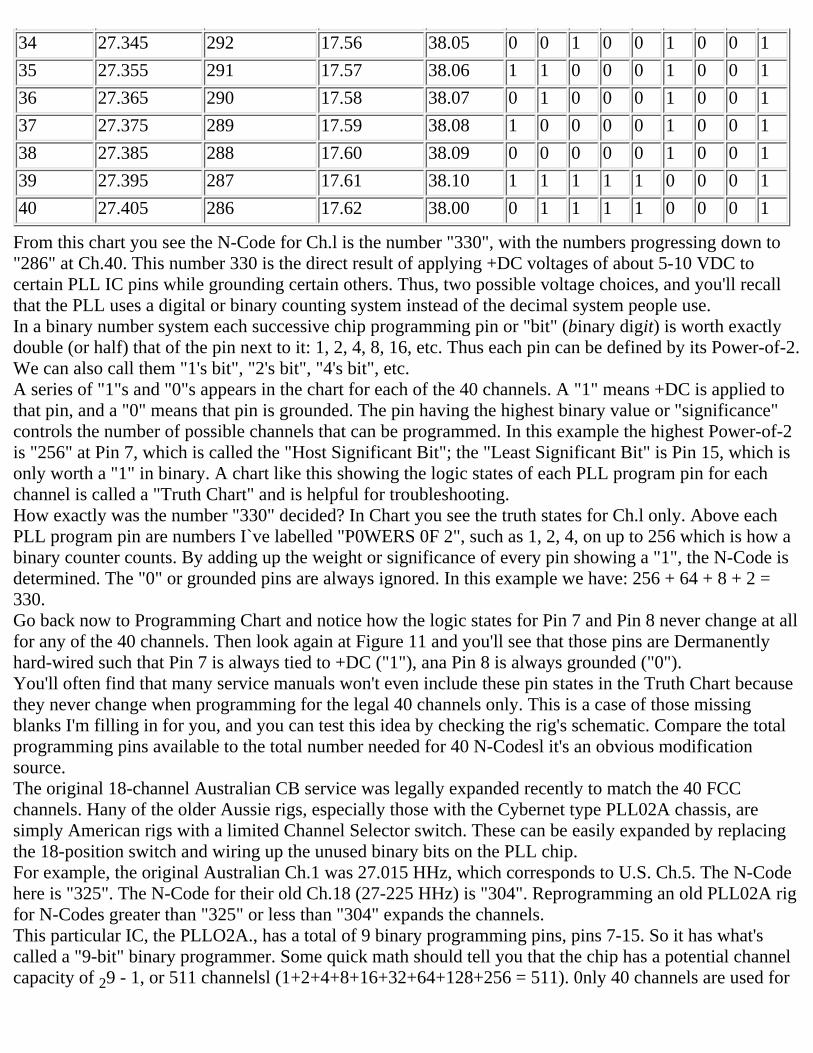
34 27.345 292 17.56 38.05 0 0 1 0 0 1 0 0 1
35 27.355 291 17.57 38.06 1 1 0 0 0 1 0 0 1
36 27.365 290 17.58 38.07 0 1 0 0 0 1 0 0 1
37 27.375 289 17.59 38.08 1 0 0 0 0 1 0 0 1
38 27.385 288 17.60 38.09 0 0 0 0 0 1 0 0 1
39 27.395 287 17.61 38.10 1 1 1 1 1 0 0 0 1
40 27.405 286 17.62 38.00 0 1 1 1 1 0 0 0 1
From this chart you see the N-Code for Ch.l is the number "330", with the numbers progressing down to"286" at Ch.40. This number 330 is the direct result of applying +DC voltages of about 5-10 VDC tocertain PLL IC pins while grounding certain others. Thus, two possible voltage choices, and you'll recallthat the PLL uses a digital or binary counting system instead of the decimal system people use.In a binary number system each successive chip programming pin or "bit" (binary digit) is worth exactlydouble (or half) that of the pin next to it: 1, 2, 4, 8, 16, etc. Thus each pin can be defined by its Power-of-2.We can also call them "1's bit", "2's bit", "4's bit", etc.A series of "1"s and "0"s appears in the chart for each of the 40 channels. A "1" means +DC is applied tothat pin, and a "0" means that pin is grounded. The pin having the highest binary value or "significance"controls the number of possible channels that can be programmed. In this example the highest Power-of-2is "256" at Pin 7, which is called the "Host Significant Bit"; the "Least Significant Bit" is Pin 15, which isonly worth a "1" in binary. A chart like this showing the logic states of each PLL program pin for eachchannel is called a "Truth Chart" and is helpful for troubleshooting.How exactly was the number "330" decided? In Chart you see the truth states for Ch.l only. Above eachPLL program pin are numbers I`ve labelled "P0WERS 0F 2", such as 1, 2, 4, on up to 256 which is how abinary counter counts. By adding up the weight or significance of every pin showing a "1", the N-Code isdetermined. The "0" or grounded pins are always ignored. In this example we have: 256 + 64 + 8 + 2 =330.Go back now to Programming Chart and notice how the logic states for Pin 7 and Pin 8 never change at allfor any of the 40 channels. Then look again at Figure 11 and you'll see that those pins are Dermanentlyhard-wired such that Pin 7 is always tied to +DC ("1"), ana Pin 8 is always grounded ("0").You'll often find that many service manuals won't even include these pin states in the Truth Chart becausethey never change when programming for the legal 40 channels only. This is a case of those missingblanks I'm filling in for you, and you can test this idea by checking the rig's schematic. Compare the totalprogramming pins available to the total number needed for 40 N-Codesl it's an obvious modificationsource.The original 18-channel Australian CB service was legally expanded recently to match the 40 FCCchannels. Hany of the older Aussie rigs, especially those with the Cybernet type PLL02A chassis, aresimply American rigs with a limited Channel Selector switch. These can be easily expanded by replacingthe 18-position switch and wiring up the unused binary bits on the PLL chip.For example, the original Australian Ch.1 was 27.015 HHz, which corresponds to U.S. Ch.5. The N-Codehere is "325". The N-Code for their old Ch.18 (27-225 HHz) is "304". Reprogramming an old PLL02A rigfor N-Codes greater than "325" or less than "304" expands the channels.This particular IC, the PLLO2A., has a total of 9 binary programming pins, pins 7-15. So it has what'scalled a "9-bit" binary programmer. Some quick math should tell you that the chip has a potential channelcapacity of 29 - 1, or 511 channelsl (1+2+4+8+16+32+64+128+256 = 511). 0nly 40 channels are used for
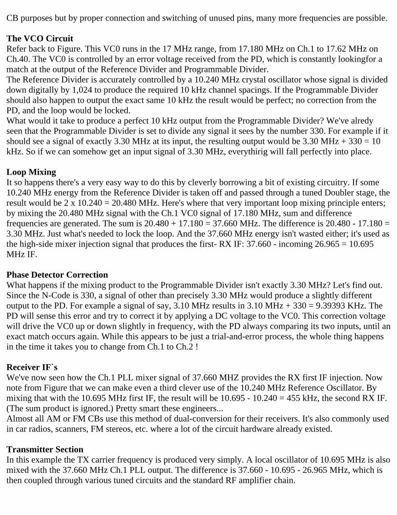
CB purposes but by proper connection and switching of unused pins, many more frequencies are possible.
The VCO CircuitRefer back to Figure. This VC0 runs in the 17 MHz range, from 17.180 MHz on Ch.1 to 17.62 MHz onCh.40. The VC0 is controlled by an error voltage received from the PD, which is constantly lookingfor amatch at the output of the Reference Divider and Programmable Divider.The Reference Divider is accurately controlled by a 10.240 MHz crystal oscillator whose signal is divideddown digitally by 1,024 to produce the required 10 kHz channel spacings. If the Programmable Dividershould also happen to output the exact same 10 kHz the result would be perfect; no correction from thePD, and the loop would be locked.What would it take to produce a perfect 10 kHz output from the Programmable Divider? We've alredyseen that the Programmable Divider is set to divide any signal it sees by the number 330. For example if itshould see a signal of exactly 3.30 MHz at its input, the resulting output would be 3.30 MHz + 330 = 10kHz. So if we can somehow get an input signal of 3.30 MHz, everythirig will fall perfectly into place.
Loop MixingIt so happens there's a very easy way to do this by cleverly borrowing a bit of existing circuitry. If some10.240 MHz energy from the Reference Divider is taken off and passed through a tuned Doubler stage, theresult would be 2 x 10.240 = 20.480 MHz. Here's where that very important loop mixing principle enters;by mixing the 20.480 MHz signal with the Ch.1 VC0 signal of 17.180 MHz, sum and differencefrequencies are generated. The sum is 20.480 + 17.180 = 37.660 MHz. The difference is 20.480 - 17.180 =3.30 MHz. Just what's needed to lock the loop. And the 37.660 MHz energy isn't wasted either; it's used asthe high-side mixer injection signal that produces the first- RX IF: 37.660 - incoming 26.965 = 10.695MHz IF.
Phase Detector CorrectionWhat happens if the mixing product to the Programmable Divider isn't exactly 3.30 MHz? Let's find out.Since the N-Code is 330, a signal of other than precisely 3.30 MHz would produce a slightly differentoutput to the PD. For example a signal of say, 3.10 MHz results in 3.10 MHz + 330 = 9.39393 KHz. ThePD will sense this error and try to correct it by applying a DC voltage to the VC0. This correction voltagewill drive the VC0 up or down slightly in frequency, with the PD always comparing its two inputs, until anexact match occurs again. While this appears to be just a trial-and-error process, the whole thing happensin the time it takes you to change from Ch.1 to Ch.2 !
Receiver IF`sWe've now seen how the Ch.1 PLL mixer signal of 37.660 MHZ provides the RX first IF injection. Nownote from Figure that we can make even a third clever use of the 10.240 MHz Reference Oscillator. Bymixing that with the 10.695 MHz first IF, the result will be 10.695 - 10.240 = 455 kHz, the second RX IF.(The sum product is ignored.) Pretty smart these engineers...Almost all AM or FM CBs use this method of dual-conversion for their receivers. It's also commonly usedin car radios, scanners, FM stereos, etc. where a lot of the circuit hardware already existed.
Transmitter SectionIn this example the TX carrier frequency is produced very simply. A local oscillator of 10.695 MHz is alsomixed with the 37.660 MHz Ch.1 PLL output. The difference is 37.660 - 10.695 - 26.965 MHz, which isthen coupled through various tuned circuits and the standard RF amplifier chain.
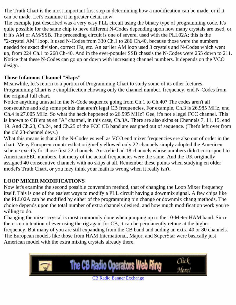
The Truth Chart is the most important first step in determining how a modification can be made. or if itcan be made. Let's examine it in greater detail now.The exemple just described was a very easy PLL circuit using the binary type of programming code. It'squite possible for the same chip to heve different N-Codes depending upon how many crystals are used, orif it's AM or AM/SSB. The preceeding circuit is one of severel used with the PLL02A; this is the"2-crystel AM" loop. It used N-Codes from 330 Ch.1 to 286 Ch.40, because those were the numbersneeded for exact division, correct IFs, etc. An earlier AM loop used 3 crystels and N-Codes which wentup, from 224 Ch.1 to 268 Ch-40. And in the ever-populer SSB chassis the N-Codes were 255 down to 211.Notice that these N-Codes can go up or down with increasing channel numbers. It depends on the VCOdesign.
Those Infamous Channel "Skips"Meanwhile, let's return to a portion of Programming Chart to study some of its other feetures.Programming Chart is e eimplificetion ehowing only the channel number, frequency, end N-Codes fromthe original full chart.Notice anything unusual in the N-Code sequence going from Ch.1 to Ch.40? The codes aren't allconsecutive and skip some points that aren't legal CB frequencies. For example, Ch.3 is 26.985 MHz, endCh.4 is 27.005 MHz. So what the heck heppened to 26.995 MHz? Gee, it's not e legel FCC channel. Thisis known to CB`ers as en "A" channel, in this case, Ch.3A. There are also skips et Chennels 7, 11, 15, end19. And Ch.23, Ch.24, end Ch.25 of the FCC CB band are essigned out of sequence. (Thet's left over fromthe old 23-chennel deys.)What this means is that all the N-Codes es well as VCO end mixer frequencies ere also out of order in thechart. Meny Europeen countriesthat originelly ellowed only 22 channels simply adopted the Americenscheme exectly for those first 22 channels. Austrelie had 18 channels whose numbers didn't correspond toAmerican/EEC numbers, but meny of the actual frequencies were the same. And the UK originellyassigned 40 consecutive channels with no skips at all. Remember these points when studying en oldermodel's Truth Chart, or you mey think your math is wrong when it really isn't.
LOOP MIXER MODIFICATIONSNow let's examine the second possible conversion method, that of changing the Loop Mixer frequencyitself. This is one of the easiest ways to modify a PLL circuit having a downmix signal. A few chips likethe PLL02A can be modified by either of the programming pin change or downmix chang methods. Thechoice depends upon the total number of extra channels desired, and how much modification work you'rewilling to do.Changing the mixer crystal is most commonly done when jumping up to the 10-Meter HAM band. Sincethere's no intention of ever using the rig again for CB, it can be permanently retune at the higherfrequency. But many of you are still expanding from the CB band and adding an extra 40 or 80 channels.The European models like those from HAM International, Major, and SuperStar were basically justAmerican model with the extra mixing crystals already there.
CB Radio Banner Exchange
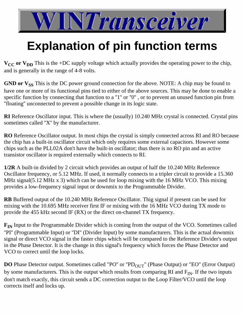
Explanation of pin function termsVCC or VDD This is the +DC supply voltage which actually provides the operating power to the chip,and is generally in the range of 4-8 volts.
GND or VSS This is the DC power ground connection for the above. NOTE: A chip may be found tohave one or more of its functional pins tied to either of the above sources. This may be done to enable aspecific function by connecting that function to a ''1'' or ''0'' , or to prevent an unused function pin from''floating'' unconnected to prevent a possible change in its logic state.
RI Reference Oscillator input. This is where the (usually) 10.240 MHz crystal is connected. Crystal pinssometimes called ''X'' by the manufacturer.
RO Reference Oscillator output. In most chips the crystal is simply connected across RI and RO becausethe chip has a built-in oscillator circuit which only requires some external capacitors. However somechips such as the PLL02A don't have the built-in oscillator; thus there is no RO pin and an activetransistor oscillator is required externally which connects to RI.
1/2R A built-in divided by 2 circuit which provides an output of half the 10.240 MHz ReferenceOscillator frequency, or 5.12 MHz. If used, it normally connects to a tripler circuit to provide a 15.360MHz signal(5.12 MHz x 3) which can be used for loop mixing with the 16 MHz VCO. This mixingprovides a low-frequency signal input or downmix to the Programmable Divider.
RB Buffered output of the 10.240 MHz Reference Oscillator. Thig signal if present can be used formixing with the 10.695 MHz receiver first IF or mixing with the 16 MHz VCO during TX mode toprovide the 455 kHz second IF (RX) or the direct on-channel TX frequency.
FIN Input to the Programmable Divider which is coming from the output of the VCO. Sometimes called''PI'' (Programmable Input) or ''DI'' (Divider Input) by some manufacturers. This is the actual downmixsignal or direct VCO signal in the faster chips which will be compared to the Reference Divider's outputin the Phase Detector. It is the change in this signal's frequency which forces the Phase Detector andVCO to correct until the loop locks.
DO Phase Detector output. Sometimes called "PO'' or ''PDOUT" (Phase Output) or "EO" (Error Output)by some manufacturers. This is the output which results from comparing RI and FIN. If the two inputsdon't match exactly, this circuit sends a DC correction output to the Loop Filter/VCO until the loopcorrects itself and locks up.
LD Lock Detector. Sometimes called "LM" (Lock Monitor) by some manufacturers.This is a secondoutput of the Phase Detector which is used to kill the transmitter (and sometimes the receiver) if the loopis not locked and operating correctly. Some chips have more than one Lock Detector pin and thus you'llsometimes see''LD1'' and "LD2" on the specs. When two Lock Detectorg are used, their normal outputsare usually opposite logicstates; i.e., one LD ig normally ''1'' and the other is normally ''0''.This is aconvenient design feature which allows the manufacturer some flexibility because he can have a choiceofinhibiting circuits; some work with LOW outputs,some work with HIGH outputs. Some rigg use bothLD pins in their circuits.
MC Misprogram Code Detector. The same idea as the Lock Detector, this is found in the newer ROMchips. If you try to force an illegal program code on the chip, this pin is activated and will kill thetransmitter, receiver, or in some cases, call up Ch.9 or Ch.19 instead.
T/R Transmit/Receive switch. This is used to provide the 455 kHz offset for the receiver's second IFstage in dual-conversion AM or FM rigs. Pressing the mike button changes this pin's logic state to itsopposite state from the RX Mode.This shifts the ROM controlling the Programmable Divider, and insome chips also shifts the output of the Reference Divider from standard 5 kHz steps to 2.5 kHz steps.The T/R shift is the reason you`ll see two different sets of N-Codes and VCO frequencies in a rig' sservice manual.NOTE: Some manufacturers' chip spec sheets show a bar (-) above some pin functions, such as LM, T/R,etc. This bar is a digital logic symbol which indicates what state (''1'' or ''0'') th'at pin is in when activated.For example, theT/R with the bar notation means that the pin is normally HIGH ("1") in the ReceiveMode and normally LOW ("0") in the Transmit Mode. /LM means the Lock Monitor is "active LOW". ,i.e., it is normally HIGH but goes LOW if the loop is unlocked.
FS Frequency Select. This is a feature of some chips which allows them to synthesize frequencies ineither 10 kHz CB steps, or 5 kHz steps. Remember, some older chips such as the PLLO2A were intendedfor other uses besides CB, such as VHF marine radios, aircraft radios, etc., where 5 kHz channel spacingis common. In addition, this feature often makes it easier to synthesize SSB frequencies as well asAM/FM although the feature hasn't been used much for this. Depending upon whether the chip has aninternal pull-up or pull-down resistor here, it is generally connected to produce 10 kHz CB spacings inthe older chips. The newer chips having a T/R shift must use the 5 kHz spacing when the T/R pin is alsoused. IMPORTANT: You can't use this function to get 5 kHz channel spacings, because theProgrammable divider must also change to match the spacing.
AI and AO Active Loop Filter Amplifier input and output. This circuit if present is used to smooth outthe digital waveform coming from the Phase Detector, before it's applied to the VCO (See text.) Thisfilter is found in the newer CB-only chips. The older chips (Eg, PLL02A) require external passive filtersusing capacitors and resistors. In many rigs you'll find that these pins are connected either directly orthrough a resistor so that they are placed in series betw een the Phase Detector output pin and the VCOinput.
FIL Active filter. W e're using this designation in certain very old chips when the exact spec sheets arenot available but it's known from studying the chip's wiring in the rig that the pins are in fact part of aloop filter.
T and Q This is a wave-shaping circuit found in a few NEC chips (uPD2810, uPD2814, uPD2816, anduPD2824). It adds design flexibility but is often not even connected. This circuit consistsofan inputamplifier and a ''flip-flop'', and its purposeis to change asine-wave input (T) to a square-wave output (Q)which is more compatible with digital electronic circuits.
P0 ..... P10 Program Select pins from Channel Selector switch. (Sometimes called "D" for ''Data'' ratherthan "P" for ''Program''.) These pins control the actual channel selection. They may control selectionthrough straight binary coding, BCD, or ROM. The sub-numbers indicate the weight or significance ofeach pin. For example if there were 8 programming pins, P1 to P8, P1 would be in the "least significantbit" and P8 would bethe "most significant bit".The higher the sub-number, the greater the weight of thatpin.
NC No Connection. An unused pin May actually be disconnected inside the chip, or simply not used forthat particular rig' s PLL circuit.
CB Radio Banner Exchange
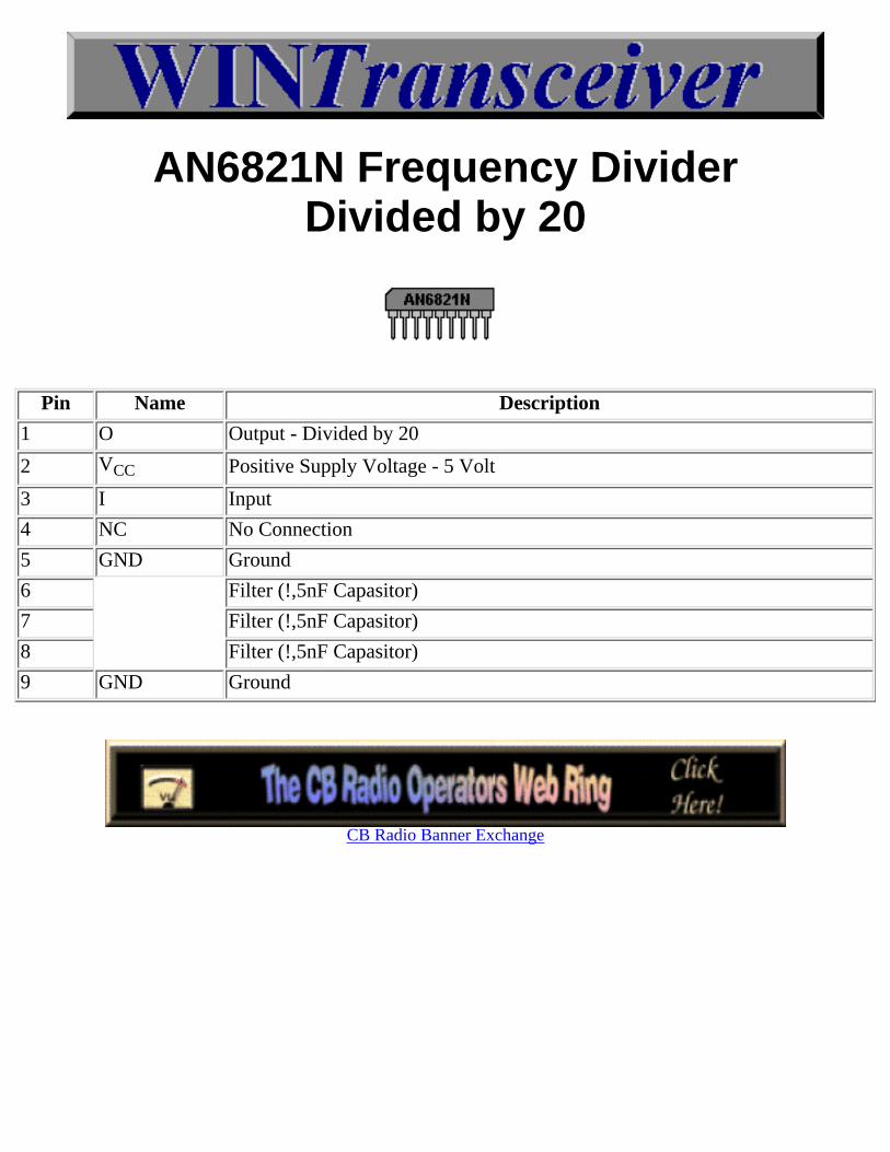
AN6821N Frequency DividerDivided by 20
Pin Name Description
1 O Output - Divided by 20
2 VCC Positive Supply Voltage - 5 Volt
3 I Input
4 NC No Connection
5 GND Ground
6 Filter (!,5nF Capasitor)
7 Filter (!,5nF Capasitor)
8 Filter (!,5nF Capasitor)
9 GND Ground
CB Radio Banner Exchange
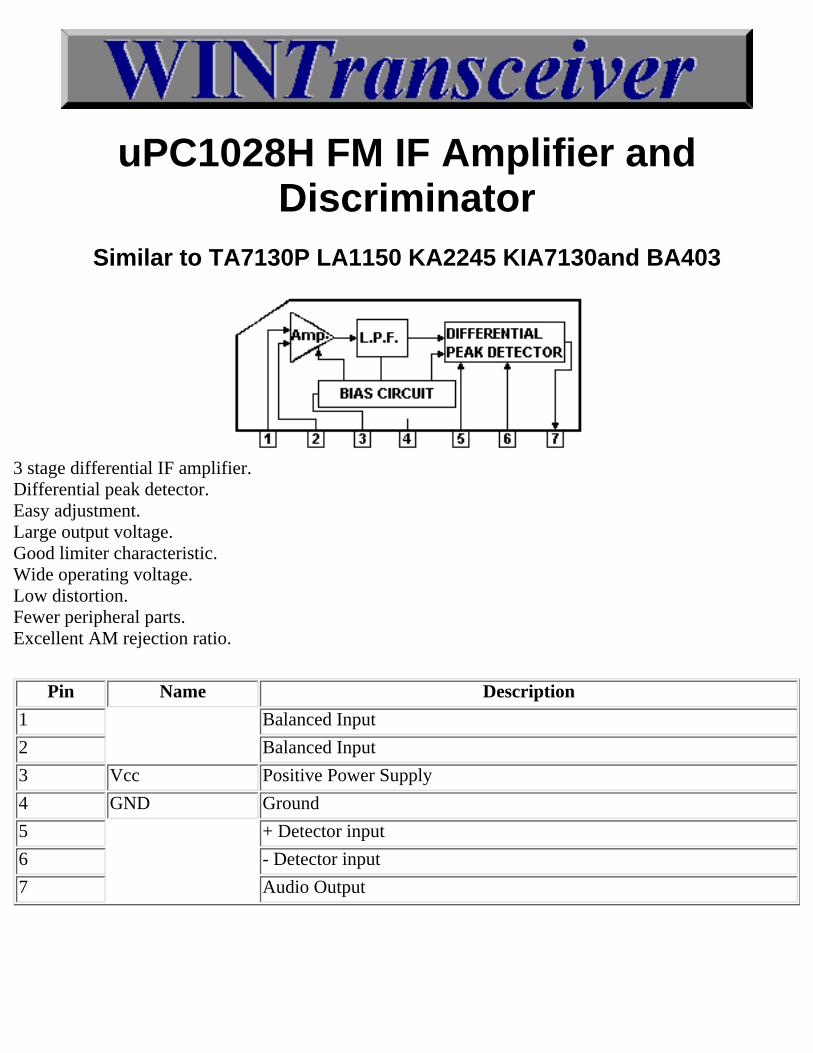
uPC1028H FM IF Amplifier andDiscriminator
Similar to TA7130P LA1150 KA2245 KIA7130and BA403
3 stage differential IF amplifier.Differential peak detector.Easy adjustment.Large output voltage.Good limiter characteristic.Wide operating voltage.Low distortion.Fewer peripheral parts.Excellent AM rejection ratio.
Pin Name Description
1 Balanced Input
2 Balanced Input
3 Vcc Positive Power Supply
4 GND Ground
5 + Detector input
6 - Detector input
7 Audio Output

CB Radio Banner Exchange
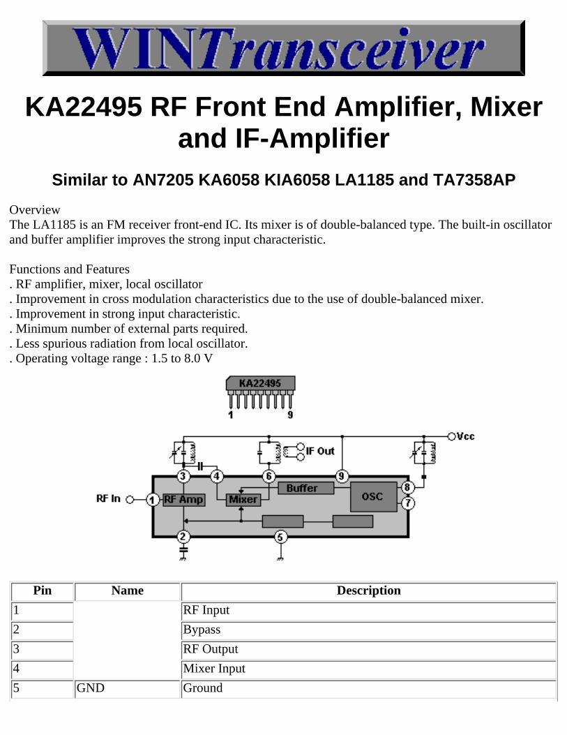
KA22495 RF Front End Amplifier, Mixerand IF-Amplifier
Similar to AN7205 KA6058 KIA6058 LA1185 and TA7358AP
OverviewThe LA1185 is an FM receiver front-end IC. Its mixer is of double-balanced type. The built-in oscillatorand buffer amplifier improves the strong input characteristic.
Functions and Features. RF amplifier, mixer, local oscillator. Improvement in cross modulation characteristics due to the use of double-balanced mixer.. Improvement in strong input characteristic.. Minimum number of external parts required.. Less spurious radiation from local oscillator.. Operating voltage range : 1.5 to 8.0 V
Pin Name Description
1 RF Input
2 Bypass
3 RF Output
4 Mixer Input
5 GND Ground

6 Mixer Output
7 Oscillator Monitor
8 Oscillator Input
9 Vcc Positive Power Supply
CB Radio Banner Exchange
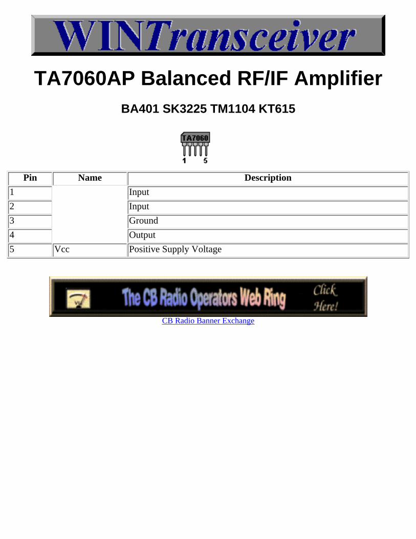
TA7060AP Balanced RF/IF AmplifierBA401 SK3225 TM1104 KT615
Pin Name Description
1 Input
2 Input
3 Ground
4 Output
5 Vcc Positive Supply Voltage
CB Radio Banner Exchange
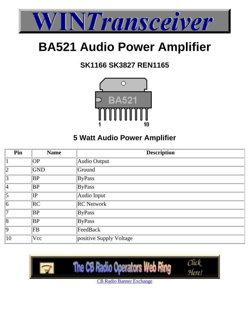
BA521 Audio Power AmplifierSK1166 SK3827 REN1165
5 Watt Audio Power Amplifier
Pin Name Description
1 OP Audio Output
2 GND Ground
3 BP ByPass
4 BP ByPass
5 IP Audio Input
6 RC RC Network
7 BP ByPass
8 BP ByPass
9 FB FeedBack
10 Vcc positive Supply Voltage
CB Radio Banner Exchange
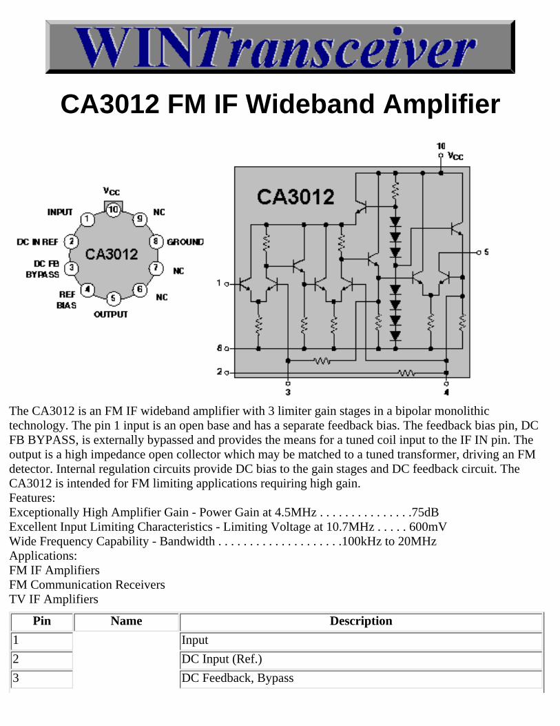
CA3012 FM IF Wideband Amplifier
The CA3012 is an FM IF wideband amplifier with 3 limiter gain stages in a bipolar monolithictechnology. The pin 1 input is an open base and has a separate feedback bias. The feedback bias pin, DCFB BYPASS, is externally bypassed and provides the means for a tuned coil input to the IF IN pin. Theoutput is a high impedance open collector which may be matched to a tuned transformer, driving an FMdetector. Internal regulation circuits provide DC bias to the gain stages and DC feedback circuit. TheCA3012 is intended for FM limiting applications requiring high gain.Features:Exceptionally High Amplifier Gain - Power Gain at 4.5MHz . . . . . . . . . . . . . . .75dBExcellent Input Limiting Characteristics - Limiting Voltage at 10.7MHz . . . . . 600mVWide Frequency Capability - Bandwidth . . . . . . . . . . . . . . . . . . . .100kHz to 20MHzApplications:FM IF AmplifiersFM Communication ReceiversTV IF Amplifiers
Pin Name Description
1 Input
2 DC Input (Ref.)
3 DC Feedback, Bypass
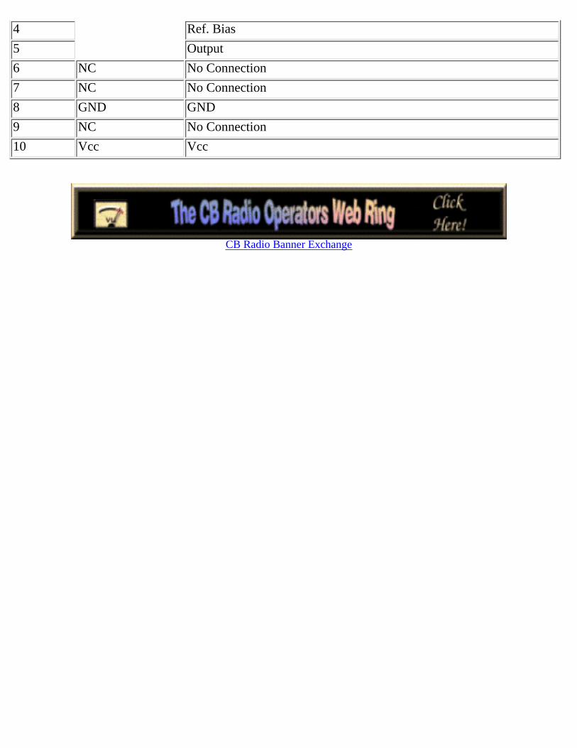
4 Ref. Bias
5 Output
6 NC No Connection
7 NC No Connection
8 GND GND
9 NC No Connection
10 Vcc Vcc
CB Radio Banner Exchange
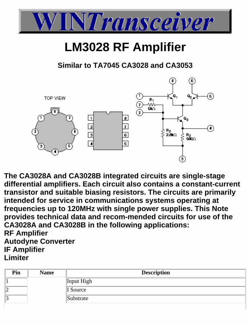
LM3028 RF AmplifierSimilar to TA7045 CA3028 and CA3053
The CA3028A and CA3028B integrated circuits are single-stagedifferential amplifiers. Each circuit also contains a constant-currenttransistor and suitable biasing resistors. The circuits are primarilyintended for service in communications systems operating atfrequencies up to 120MHz with single power supplies. This Noteprovides technical data and recom-mended circuits for use of theCA3028A and CA3028B in the following applications:RF AmplifierAutodyne ConverterIF AmplifierLimiter
Pin Name Description
1 Input High
2 I Source
3 Substrate

4 I Source Em.
5 Input Low
6 Output High
7 AGC (AutomaticGainControl)
8 Output Low
CB Radio Banner Exchange
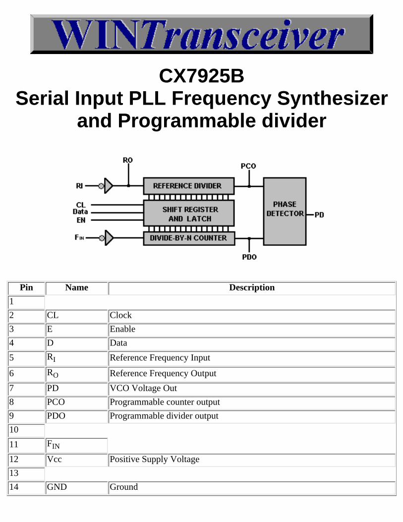
CX7925BSerial Input PLL Frequency Synthesizer
and Programmable divider
Pin Name Description
1
2 CL Clock
3 E Enable
4 D Data
5 RI Reference Frequency Input
6 RO Reference Frequency Output
7 PD VCO Voltage Out
8 PCO Programmable counter output
9 PDO Programmable divider output
10
11 FIN
12 Vcc Positive Supply Voltage
13
14 GND Ground

CB Radio Banner Exchange
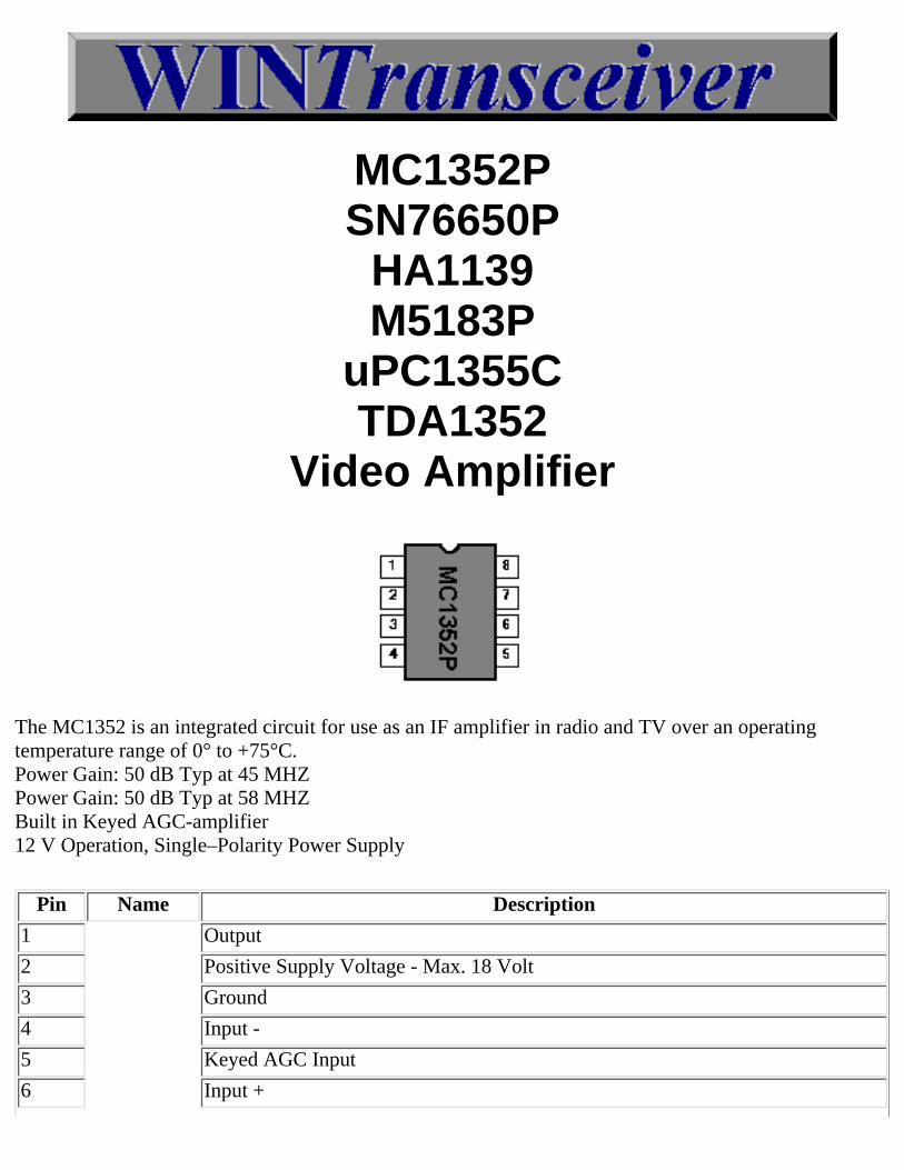
MC1352PSN76650P
HA1139M5183P
uPC1355CTDA1352
Video Amplifier
The MC1352 is an integrated circuit for use as an IF amplifier in radio and TV over an operatingtemperature range of 0° to +75°C.Power Gain: 50 dB Typ at 45 MHZPower Gain: 50 dB Typ at 58 MHZBuilt in Keyed AGC-amplifier12 V Operation, Single–Polarity Power Supply
Pin Name Description
1 Output
2 Positive Supply Voltage - Max. 18 Volt
3 Ground
4 Input -
5 Keyed AGC Input
6 Input +

7 Ground
8 Output
CB Radio Banner Exchange
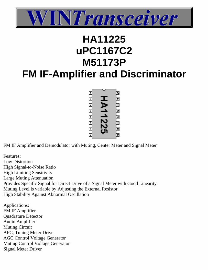
HA11225uPC1167C2
M51173PFM IF-Amplifier and Discriminator
FM IF Amplifier and Demodulator with Muting, Center Meter and Signal Meter
Features:Low DistortionHigh Signal-to-Noise RatioHigh Limiting SensitivityLarge Muting AttenuationProvides Specific Signal for Direct Drive of a Signal Meter with Good LinearityMuting Level is variable by Adjusting the External ResistorHigh Stability Against Abnormal Oscillation
Applications:FM IF AmplifierQuadrature DetectorAudio AmplifierMuting CircuitAFC, Tuning Meter DriverAGC Control Voltage GeneratorMuting Control Voltage GeneratorSignal Meter Driver
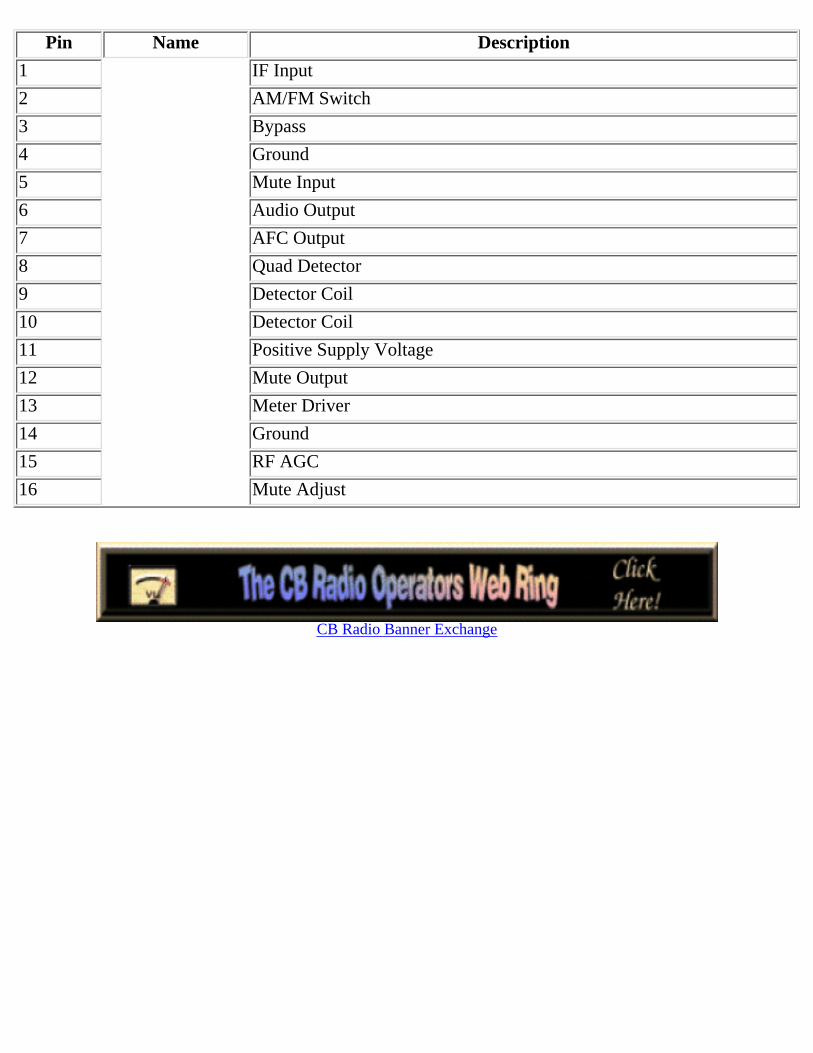
Pin Name Description
1 IF Input
2 AM/FM Switch
3 Bypass
4 Ground
5 Mute Input
6 Audio Output
7 AFC Output
8 Quad Detector
9 Detector Coil
10 Detector Coil
11 Positive Supply Voltage
12 Mute Output
13 Meter Driver
14 Ground
15 RF AGC
16 Mute Adjust
CB Radio Banner Exchange
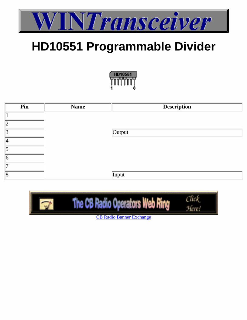
HD10551 Programmable Divider
Pin Name Description
1
2
3 Output
4
5
6
7
8 Input
CB Radio Banner Exchange
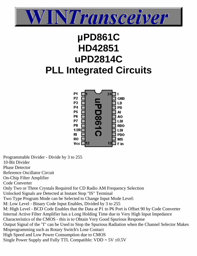
µPD861CHD42851
uPD2814CPLL Integrated Circuits
Programmable Divider - Divide by 3 to 25510-Bit DividerPhase DetectorReference Oscillator CircuitOn-Chip Filter AmplifierCode ConverterOnly Two or Three Crystals Required for CD Radio AM Frequency SelectionUnlocked Signals are Detected at Instant Stop "IS" TerminalTwo Type Program Mode can be Selected to Change Input Mode Level:M: Low Level - Binary Code Input Enables, Divided by 3 to 255M: High Level - BCD Code Enables that the Data at P1 to P6 Port is Offset 90 by Code ConverterInternal Active Filter Amplifier has a Long Holding Time due to Very High Input ImpedanceCharacteristics of the CMOS - this is to Obtain Very Good Spurious ResponseOutput Signal of the "I" can be Used to Stop the Spurious Radiation when the Channel Selector MakesMisprogramming such as Rotary Switch's Lose ContactHigh Speed and Low Power Consumption due to CMOSSingle Power Supply and Fully TTL Compatible: VDD = 5V ±0.5V
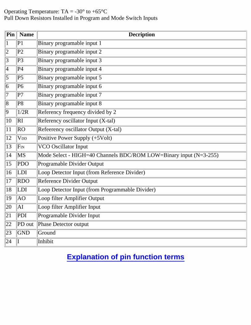
Operating Temperature: TA = -30° to +65°CPull Down Resistors Installed in Program and Mode Switch Inputs
Pin Name Decription
1 P1 Binary programable input 1
2 P2 Binary programable input 2
3 P3 Binary programable input 3
4 P4 Binary programable input 4
5 P5 Binary programable input 5
6 P6 Binary programable input 6
7 P7 Binary programable input 7
8 P8 Binary programable input 8
9 1/2R Referency frequency divided by 2
10 RI Referency oscillator Input (X-tal)
11 RO Refeerency oscillator Output (X-tal)
12 VDD Positive Power Supply (+5Volt)
13 FIN VCO Oscillator Input
14 MS Mode Select - HIGH=40 Channels BDC/ROM LOW=Binary input (N=3-255)
15 PDO Programable Divider Output
16 LDI Loop Detector Input (from Reference Divider)
17 RDO Reference Divider Output
18 LDI Loop Detector Input (from Programmable Divider)
19 AO Loop filter Amplifier Output
20 AI Loop filter Amplifier Input
21 PDI Programable Divider Input
22 PD out Phase Detector output
23 GND Ground
24 I Inhibit
Explanation of pin function terms

µPD2814 µPD2816 HD42853 KM5624 PLLIntegrated Circuits
Overview
This 27 MHz band, PLL frequency synthesizer LSI chip is designed specifically for CB transceivers. Theintegrated circuit`s incorporates PLL circuitry and a controller for CB applications on a single CMOSchip.This PLL-circuit use a 6 bit ROM programmable divide-by-N counter. The ROM-table is programmedfrom factory to 40 channels CEPT.
Down-converting of the frequency to the divider
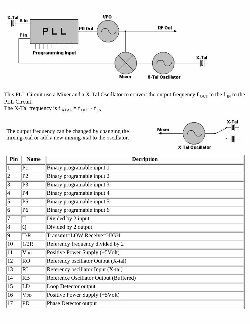
This PLL Circuit use a Mixer and a X-Tal Oscillator to convert the output frequency f OUT to the f IN to thePLL Circuit.The X-Tal frequency is f XTAL = f OUT - f IN
The output frequency can be changed by changing themixing-xtal or add a new mixing-xtal to the oscillator.
Pin Name Decription
1 P1 Binary programable input 1
2 P2 Binary programable input 2
3 P3 Binary programable input 3
4 P4 Binary programable input 4
5 P5 Binary programable input 5
6 P6 Binary programable input 6
7 T Divided by 2 input
8 Q Divided by 2 output
9 T/R Transmit=LOW Receive=HIGH
10 1/2R Referency frequency divided by 2
11 VDD Positive Power Supply (+5Volt)
12 RO Referency oscillator Output (X-tal)
13 RI Referency oscillator Input (X-tal)
14 RB Reference Oscillator Output (Buffered)
15 LD Loop Detector output
16 VDD Positive Power Supply (+5Volt)
17 PD Phase Detector output
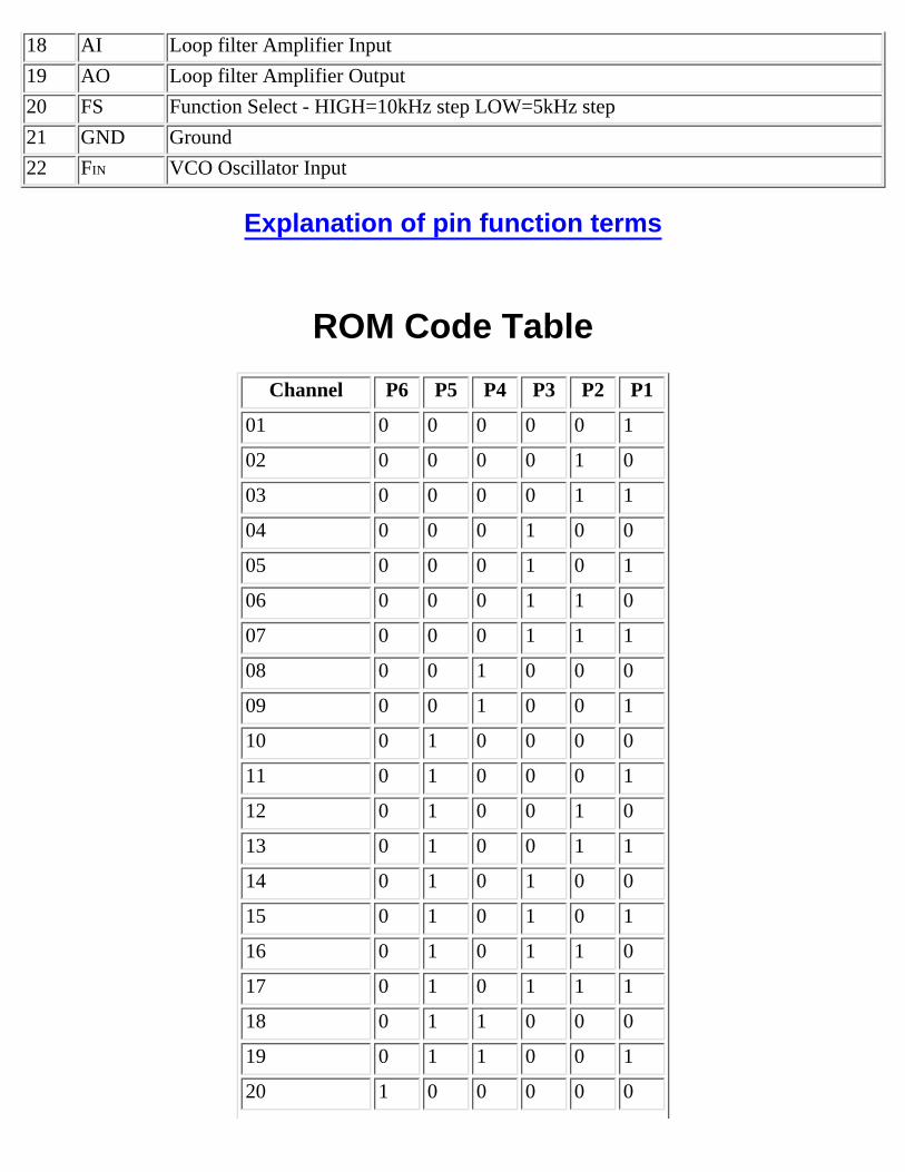
18 AI Loop filter Amplifier Input
19 AO Loop filter Amplifier Output
20 FS Function Select - HIGH=10kHz step LOW=5kHz step
21 GND Ground
22 FIN VCO Oscillator Input
Explanation of pin function terms
ROM Code Table
Channel P6 P5 P4 P3 P2 P1
01 0 0 0 0 0 1
02 0 0 0 0 1 0
03 0 0 0 0 1 1
04 0 0 0 1 0 0
05 0 0 0 1 0 1
06 0 0 0 1 1 0
07 0 0 0 1 1 1
08 0 0 1 0 0 0
09 0 0 1 0 0 1
10 0 1 0 0 0 0
11 0 1 0 0 0 1
12 0 1 0 0 1 0
13 0 1 0 0 1 1
14 0 1 0 1 0 0
15 0 1 0 1 0 1
16 0 1 0 1 1 0
17 0 1 0 1 1 1
18 0 1 1 0 0 0
19 0 1 1 0 0 1
20 1 0 0 0 0 0
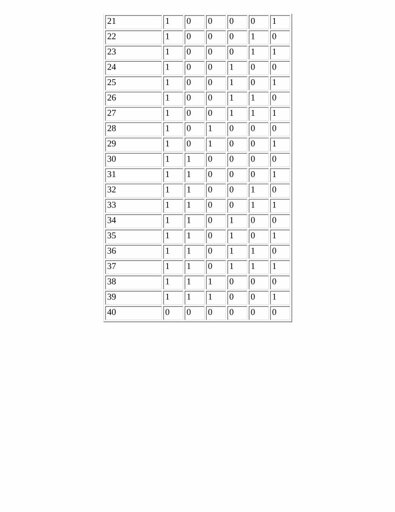
21 1 0 0 0 0 1
22 1 0 0 0 1 0
23 1 0 0 0 1 1
24 1 0 0 1 0 0
25 1 0 0 1 0 1
26 1 0 0 1 1 0
27 1 0 0 1 1 1
28 1 0 1 0 0 0
29 1 0 1 0 0 1
30 1 1 0 0 0 0
31 1 1 0 0 0 1
32 1 1 0 0 1 0
33 1 1 0 0 1 1
34 1 1 0 1 0 0
35 1 1 0 1 0 1
36 1 1 0 1 1 0
37 1 1 0 1 1 1
38 1 1 1 0 0 0
39 1 1 1 0 0 1
40 0 0 0 0 0 0
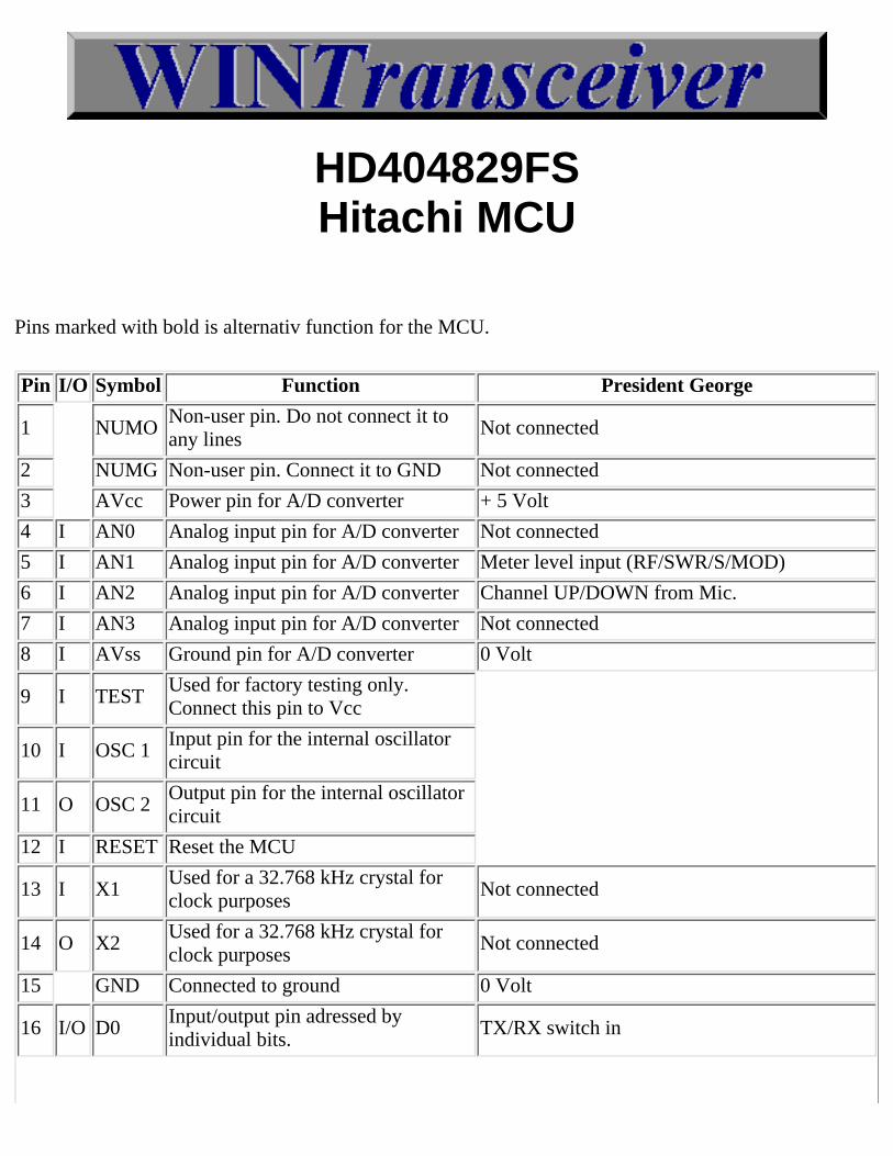
HD404829FSHitachi MCU
Pins marked with bold is alternativ function for the MCU.
Pin I/O Symbol Function President George
1 NUMONon-user pin. Do not connect it toany lines
Not connected
2 NUMG Non-user pin. Connect it to GND Not connected
3 AVcc Power pin for A/D converter + 5 Volt
4 I AN0 Analog input pin for A/D converter Not connected
5 I AN1 Analog input pin for A/D converter Meter level input (RF/SWR/S/MOD)
6 I AN2 Analog input pin for A/D converter Channel UP/DOWN from Mic.
7 I AN3 Analog input pin for A/D converter Not connected
8 I AVss Ground pin for A/D converter 0 Volt
9 I TESTUsed for factory testing only.Connect this pin to Vcc
10 I OSC 1Input pin for the internal oscillatorcircuit
11 O OSC 2Output pin for the internal oscillatorcircuit
12 I RESET Reset the MCU
13 I X1Used for a 32.768 kHz crystal forclock purposes
Not connected
14 O X2Used for a 32.768 kHz crystal forclock purposes
Not connected
15 GND Connected to ground 0 Volt
16 I/O D0Input/output pin adressed byindividual bits.
TX/RX switch in
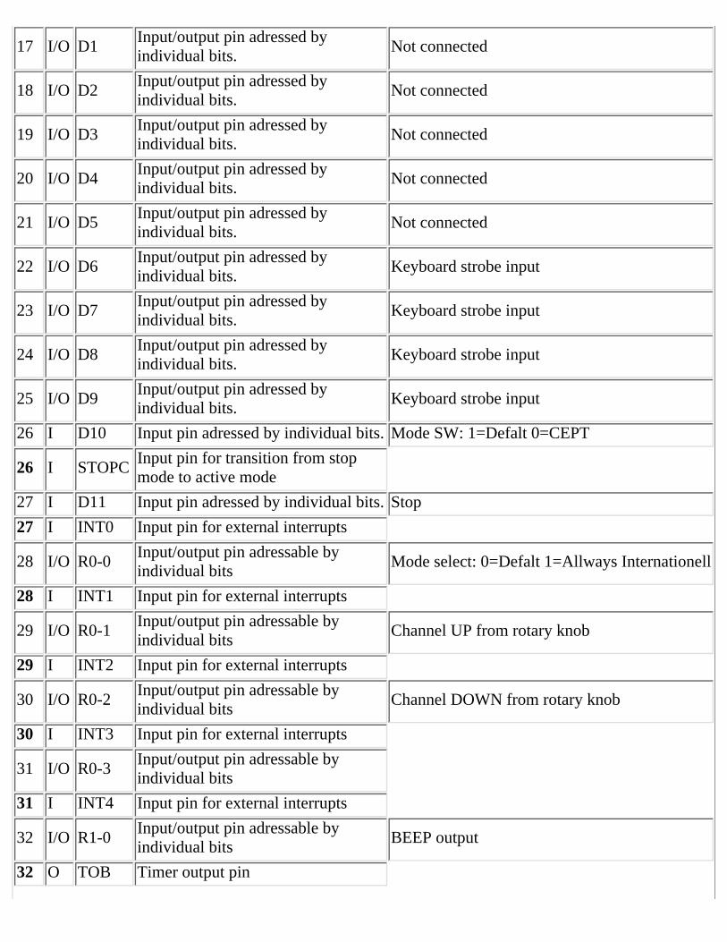
17 I/O D1Input/output pin adressed byindividual bits.
Not connected
18 I/O D2Input/output pin adressed byindividual bits.
Not connected
19 I/O D3Input/output pin adressed byindividual bits.
Not connected
20 I/O D4Input/output pin adressed byindividual bits.
Not connected
21 I/O D5Input/output pin adressed byindividual bits.
Not connected
22 I/O D6Input/output pin adressed byindividual bits.
Keyboard strobe input
23 I/O D7Input/output pin adressed byindividual bits.
Keyboard strobe input
24 I/O D8Input/output pin adressed byindividual bits.
Keyboard strobe input
25 I/O D9Input/output pin adressed byindividual bits.
Keyboard strobe input
26 I D10 Input pin adressed by individual bits. Mode SW: 1=Defalt 0=CEPT
26 I STOPCInput pin for transition from stopmode to active mode
27 I D11 Input pin adressed by individual bits. Stop
27 I INT0 Input pin for external interrupts
28 I/O R0-0Input/output pin adressable byindividual bits
Mode select: 0=Defalt 1=Allways Internationell
28 I INT1 Input pin for external interrupts
29 I/O R0-1Input/output pin adressable byindividual bits
Channel UP from rotary knob
29 I INT2 Input pin for external interrupts
30 I/O R0-2Input/output pin adressable byindividual bits
Channel DOWN from rotary knob
30 I INT3 Input pin for external interrupts
31 I/O R0-3Input/output pin adressable byindividual bits
31 I INT4 Input pin for external interrupts
32 I/O R1-0Input/output pin adressable byindividual bits
BEEP output
32 O TOB Timer output pin

33 I/O R1-1Input/output pin adressable byindividual bits
GREEN lamp
33 O TOC Timer output pin
34 I/O R1-2Input/output pin adressable byindividual bits
ORANGE lamp
34 O TOD Timer output pin
35 I/O R1-3Input/output pin adressable byindividual bits
Not connected
35 I EVNB Event count input pin Not connected
36 I/O R2-0Input/output pin adressable byindividual bits
Serial data output to EEPROM
36 I EVND Event count input pin
37 I/O R2-1Input/output pin adressable byindividual bits
Serial data input from EEPROM
37 I/O SCKSerial interface clock input/outputpin
38 I/O R2-2Input/output pin adressable byindividual bits
Chip select to EEPROM
38 I SISerial interface receive data inputpin
39 I/O R2-3Input/output pin adressable byindividual bits
Clock to EEPROM
39 O SOSerial interface transmit data outputpin
40 I/O R3-0Input/output pin adressable byindividual bits
41 I/O R3-1Input/output pin adressable byindividual bits
Keyboard strobe output
42 I/O R3-2Input/output pin adressable byindividual bits
Keyboard strobe output
43 I/O R3-3Input/output pin adressable byindividual bits
Keyboard strobe output
44 I/O R4-0Input/output pin adressable byindividual bits
Keyboard strobe output
45 I/O R4-1Input/output pin adressable byindividual bits
46 I/O R4-2Input/output pin adressable byindividual bits
Not connected
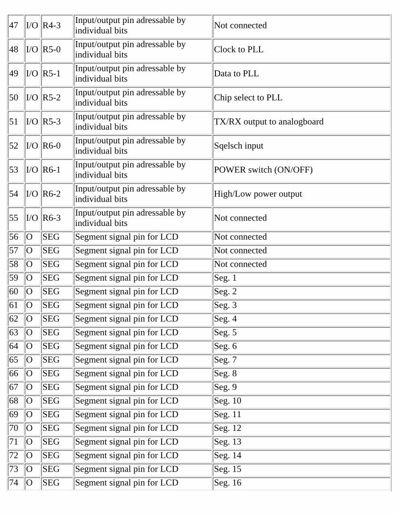
47 I/O R4-3Input/output pin adressable byindividual bits
Not connected
48 I/O R5-0Input/output pin adressable byindividual bits
Clock to PLL
49 I/O R5-1Input/output pin adressable byindividual bits
Data to PLL
50 I/O R5-2Input/output pin adressable byindividual bits
Chip select to PLL
51 I/O R5-3Input/output pin adressable byindividual bits
TX/RX output to analogboard
52 I/O R6-0Input/output pin adressable byindividual bits
Sqelsch input
53 I/O R6-1Input/output pin adressable byindividual bits
POWER switch (ON/OFF)
54 I/O R6-2Input/output pin adressable byindividual bits
High/Low power output
55 I/O R6-3Input/output pin adressable byindividual bits
Not connected
56 O SEG Segment signal pin for LCD Not connected
57 O SEG Segment signal pin for LCD Not connected
58 O SEG Segment signal pin for LCD Not connected
59 O SEG Segment signal pin for LCD Seg. 1
60 O SEG Segment signal pin for LCD Seg. 2
61 O SEG Segment signal pin for LCD Seg. 3
62 O SEG Segment signal pin for LCD Seg. 4
63 O SEG Segment signal pin for LCD Seg. 5
64 O SEG Segment signal pin for LCD Seg. 6
65 O SEG Segment signal pin for LCD Seg. 7
66 O SEG Segment signal pin for LCD Seg. 8
67 O SEG Segment signal pin for LCD Seg. 9
68 O SEG Segment signal pin for LCD Seg. 10
69 O SEG Segment signal pin for LCD Seg. 11
70 O SEG Segment signal pin for LCD Seg. 12
71 O SEG Segment signal pin for LCD Seg. 13
72 O SEG Segment signal pin for LCD Seg. 14
73 O SEG Segment signal pin for LCD Seg. 15
74 O SEG Segment signal pin for LCD Seg. 16
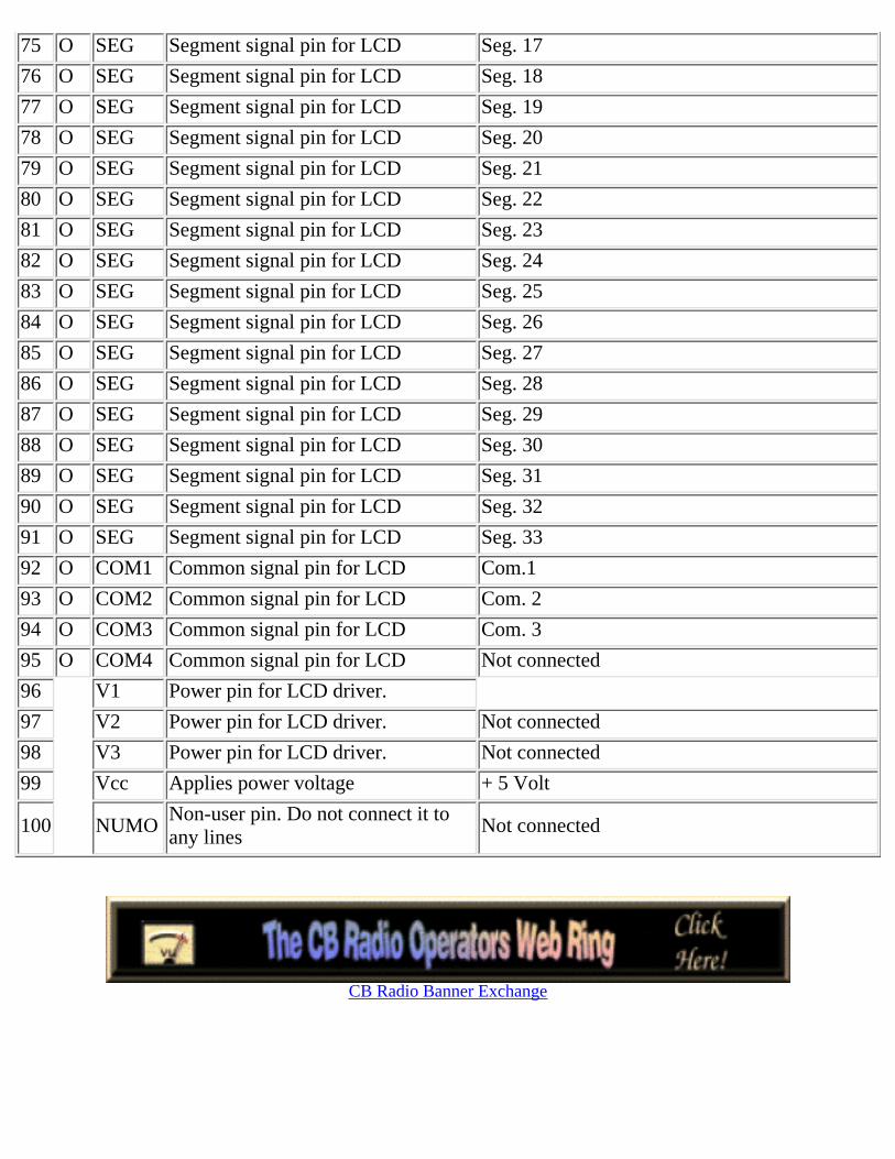
75 O SEG Segment signal pin for LCD Seg. 17
76 O SEG Segment signal pin for LCD Seg. 18
77 O SEG Segment signal pin for LCD Seg. 19
78 O SEG Segment signal pin for LCD Seg. 20
79 O SEG Segment signal pin for LCD Seg. 21
80 O SEG Segment signal pin for LCD Seg. 22
81 O SEG Segment signal pin for LCD Seg. 23
82 O SEG Segment signal pin for LCD Seg. 24
83 O SEG Segment signal pin for LCD Seg. 25
84 O SEG Segment signal pin for LCD Seg. 26
85 O SEG Segment signal pin for LCD Seg. 27
86 O SEG Segment signal pin for LCD Seg. 28
87 O SEG Segment signal pin for LCD Seg. 29
88 O SEG Segment signal pin for LCD Seg. 30
89 O SEG Segment signal pin for LCD Seg. 31
90 O SEG Segment signal pin for LCD Seg. 32
91 O SEG Segment signal pin for LCD Seg. 33
92 O COM1 Common signal pin for LCD Com.1
93 O COM2 Common signal pin for LCD Com. 2
94 O COM3 Common signal pin for LCD Com. 3
95 O COM4 Common signal pin for LCD Not connected
96 V1 Power pin for LCD driver.
97 V2 Power pin for LCD driver. Not connected
98 V3 Power pin for LCD driver. Not connected
99 Vcc Applies power voltage + 5 Volt
100 NUMONon-user pin. Do not connect it toany lines
Not connected
CB Radio Banner Exchange
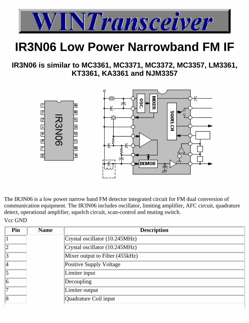
IR3N06 Low Power Narrowband FM IFIR3N06 is similar to MC3361, MC3371, MC3372, MC3357, LM3361,
KT3361, KA3361 and NJM3357
The IR3N06 is a low power narrow band FM detector integrated circuit for FM dual conversion ofcommunication equipment. The IR3N06 includes oscillator, limiting amplifier, AFC circuit, quadraturedetect, operational amplifier, squelch circuit, scan-control and muting switch.
Vcc GND
Pin Name Description
1 Crystal oscillator (10.245MHz)
2 Crystal oscillator (10.245MHz)
3 Mixer output to Filter (455kHz)
4 Positive Supply Voltage
5 Limiter input
6 Decoupling
7 Limiter output
8 Quadrature Coil input
9 Demodulator output
10 IF Filter input
11 IF Filter output
12 Squelch input
13 Scan Control
14 Audio Mute
15 Ground
16 RF / MF input (10.7MHz)
CB Radio Banner Exchange
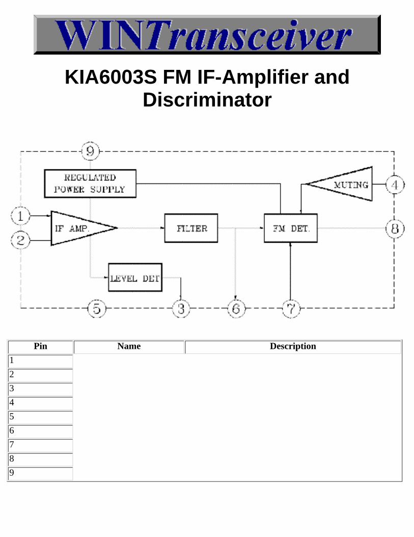
KIA6003S FM IF-Amplifier andDiscriminator
Pin Name Description
1
2
3
4
5
6
7
8
9

CB Radio Banner Exchange
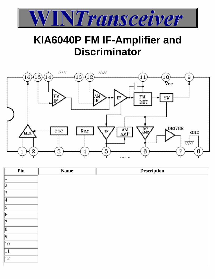
KIA6040P FM IF-Amplifier andDiscriminator
Pin Name Description
1
2
3
4
5
6
7
8
9
10
11
12
13
14
15
16
CB Radio Banner Exchange
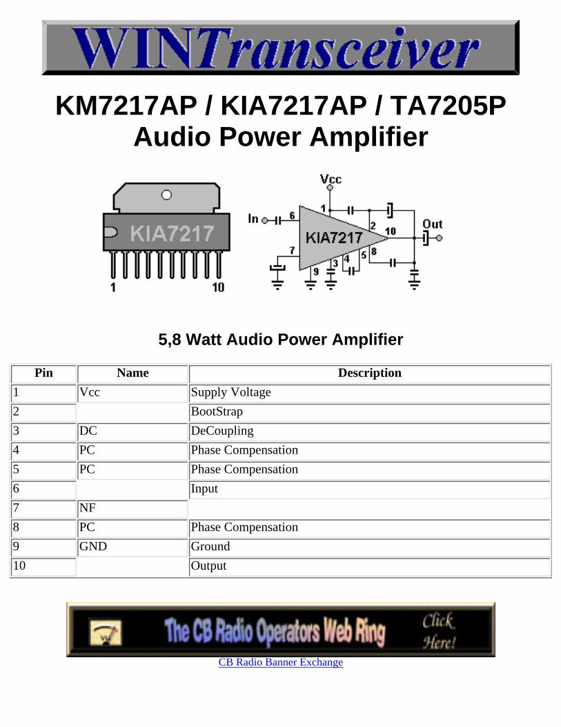
KM7217AP / KIA7217AP / TA7205PAudio Power Amplifier
5,8 Watt Audio Power Amplifier
Pin Name Description
1 Vcc Supply Voltage
2 BootStrap
3 DC DeCoupling
4 PC Phase Compensation
5 PC Phase Compensation
6 Input
7 NF
8 PC Phase Compensation
9 GND Ground
10 Output
CB Radio Banner Exchange
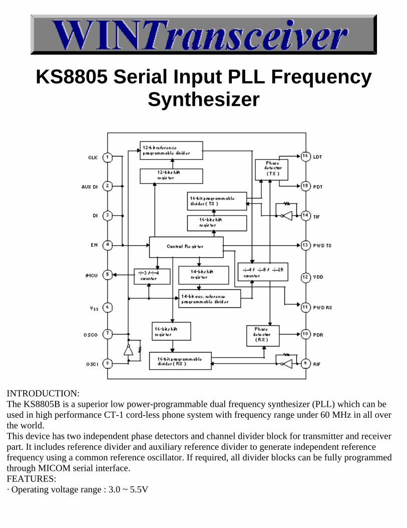
KS8805 Serial Input PLL FrequencySynthesizer
INTRODUCTION:The KS8805B is a superior low power-programmable dual frequency synthesizer (PLL) which can beused in high performance CT-1 cord-less phone system with frequency range under 60 MHz in all overthe world.This device has two independent phase detectors and channel divider block for transmitter and receiverpart. It includes reference divider and auxiliary reference divider to generate independent referencefrequency using a common reference oscillator. If required, all divider blocks can be fully programmedthrough MICOM serial interface.FEATURES:· Operating voltage range : 3.0 ~ 5.5V
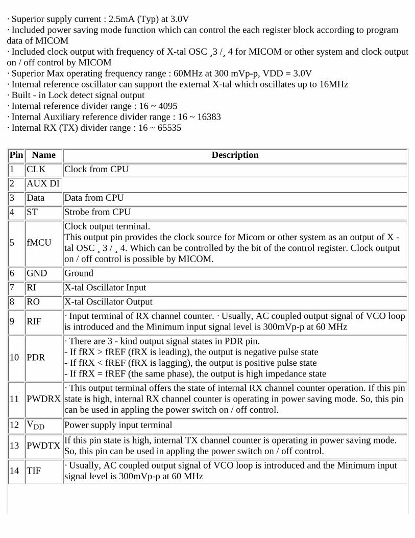
· Superior supply current : 2.5mA (Typ) at 3.0V· Included power saving mode function which can control the each register block according to programdata of MICOM· Included clock output with frequency of X-tal OSC ¸3 /¸ 4 for MICOM or other system and clock outputon / off control by MICOM· Superior Max operating frequency range : 60MHz at 300 mVp-p, VDD = 3.0V· Internal reference oscillator can support the external X-tal which oscillates up to 16MHz· Built - in Lock detect signal output· Internal reference divider range : 16 ~ 4095· Internal Auxiliary reference divider range : 16 ~ 16383· Internal RX (TX) divider range : 16 ~ 65535
Pin Name Description
1 CLK Clock from CPU
2 AUX DI
3 Data Data from CPU
4 ST Strobe from CPU
5 fMCU
Clock output terminal.This output pin provides the clock source for Micom or other system as an output of X -tal OSC ¸ 3 / ¸ 4. Which can be controlled by the bit of the control register. Clock outputon / off control is possible by MICOM.
6 GND Ground
7 RI X-tal Oscillator Input
8 RO X-tal Oscillator Output
9 RIF· Input terminal of RX channel counter. · Usually, AC coupled output signal of VCO loopis introduced and the Minimum input signal level is 300mVp-p at 60 MHz
10 PDR
· There are 3 - kind output signal states in PDR pin.- If fRX > fREF (fRX is leading), the output is negative pulse state- If fRX < fREF (fRX is lagging), the output is positive pulse state- If fRX = fREF (the same phase), the output is high impedance state
11 PWDRX· This output terminal offers the state of internal RX channel counter operation. If this pinstate is high, internal RX channel counter is operating in power saving mode. So, this pincan be used in appling the power switch on / off control.
12 VDD Power supply input terminal
13 PWDTXIf this pin state is high, internal TX channel counter is operating in power saving mode.So, this pin can be used in appling the power switch on / off control.
14 TIF· Usually, AC coupled output signal of VCO loop is introduced and the Minimum inputsignal level is 300mVp-p at 60 MHz
15 PDT
· There are 3 - kind output signal states in PDT pin.- If fTX > fREF (fTX is leading), the output is negative pulse state- If fTX < fREF (fTX is lagging), the output is positive pulse state- If fTX = fREF (the same phase), the output is high impedance state
16 LDT· Output terminal of lock detection waveformsThis output pin is internally connected with TX - loop. High output state in LDT pinindicates out of internal operation.
CB Radio Banner Exchange
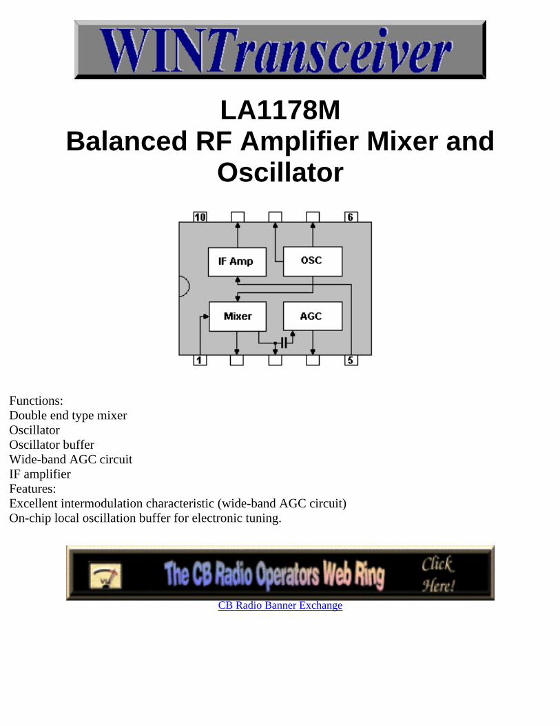
LA1178MBalanced RF Amplifier Mixer and
Oscillator
Functions:Double end type mixerOscillatorOscillator bufferWide-band AGC circuitIF amplifierFeatures:Excellent intermodulation characteristic (wide-band AGC circuit)On-chip local oscillation buffer for electronic tuning.
CB Radio Banner Exchange
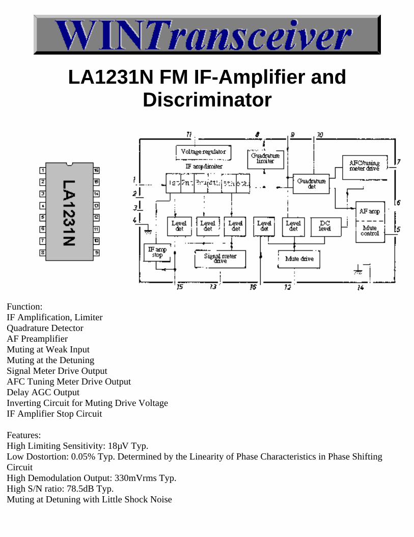
LA1231N FM IF-Amplifier andDiscriminator
Function:IF Amplification, LimiterQuadrature DetectorAF PreamplifierMuting at Weak InputMuting at the DetuningSignal Meter Drive OutputAFC Tuning Meter Drive OutputDelay AGC OutputInverting Circuit for Muting Drive VoltageIF Amplifier Stop Circuit
Features:High Limiting Sensitivity: 18µV Typ.Low Dostortion: 0.05% Typ. Determined by the Linearity of Phase Characteristics in Phase ShiftingCircuitHigh Demodulation Output: 330mVrms Typ.High S/N ratio: 78.5dB Typ.Muting at Detuning with Little Shock Noise
Single Meter Drive Output Proportional with the Input Signal Level dBDetuning Muting Band having Good SymmetricsTuning Meter Driving Output having Wide Swing WidthDelay AGC Drivce Output for Front EndConstant Voltage Circuit is Built-In: Operating Voltage range = 9V to 14VMuting Characteristics between Adjacent Stations are Distinguished
Pin Name Description
1 Front End
2 Front End
3 Front End
4 Ground
5 Mute Switch
6 AF Output
7 AF C/V ref.
8 Detector trans.
9 Detector Trans.
10 Detector Trans.
11 Positive Supply Voltage
12 Mute Switch
13 Signal Meter
14 Ground
15 AGC
16 Mute Level Adjust
CB Radio Banner Exchange
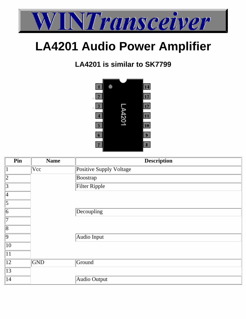
LA4201 Audio Power AmplifierLA4201 is similar to SK7799
Pin Name Description
1 Vcc Positive Supply Voltage
2 Boostrap
3 Filter Ripple
4
5
6 Decoupling
7
8
9 Audio Input
10
11
12 GND Ground
13
14 Audio Output

CB Radio Banner Exchange
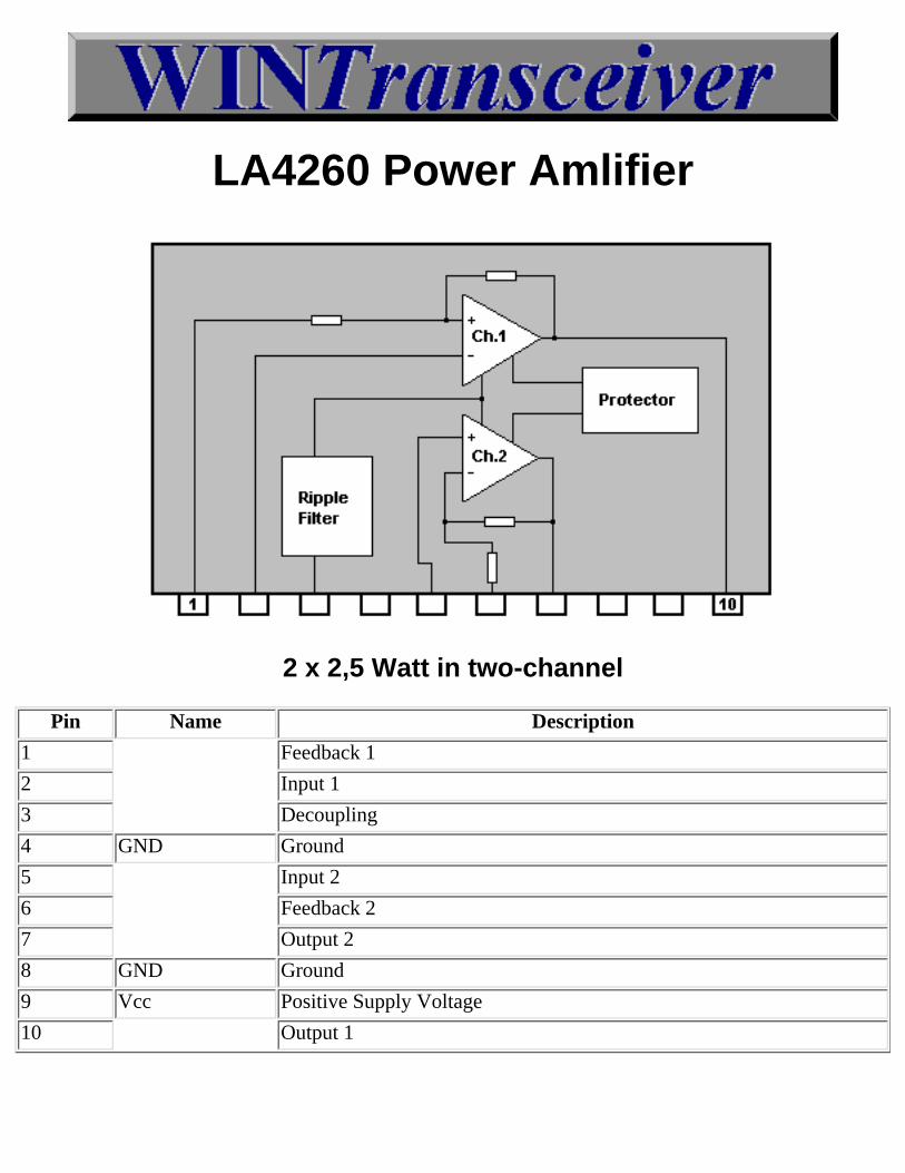
LA4260 Power Amlifier
2 x 2,5 Watt in two-channel
Pin Name Description
1 Feedback 1
2 Input 1
3 Decoupling
4 GND Ground
5 Input 2
6 Feedback 2
7 Output 2
8 GND Ground
9 Vcc Positive Supply Voltage
10 Output 1

CB Radio Banner Exchange
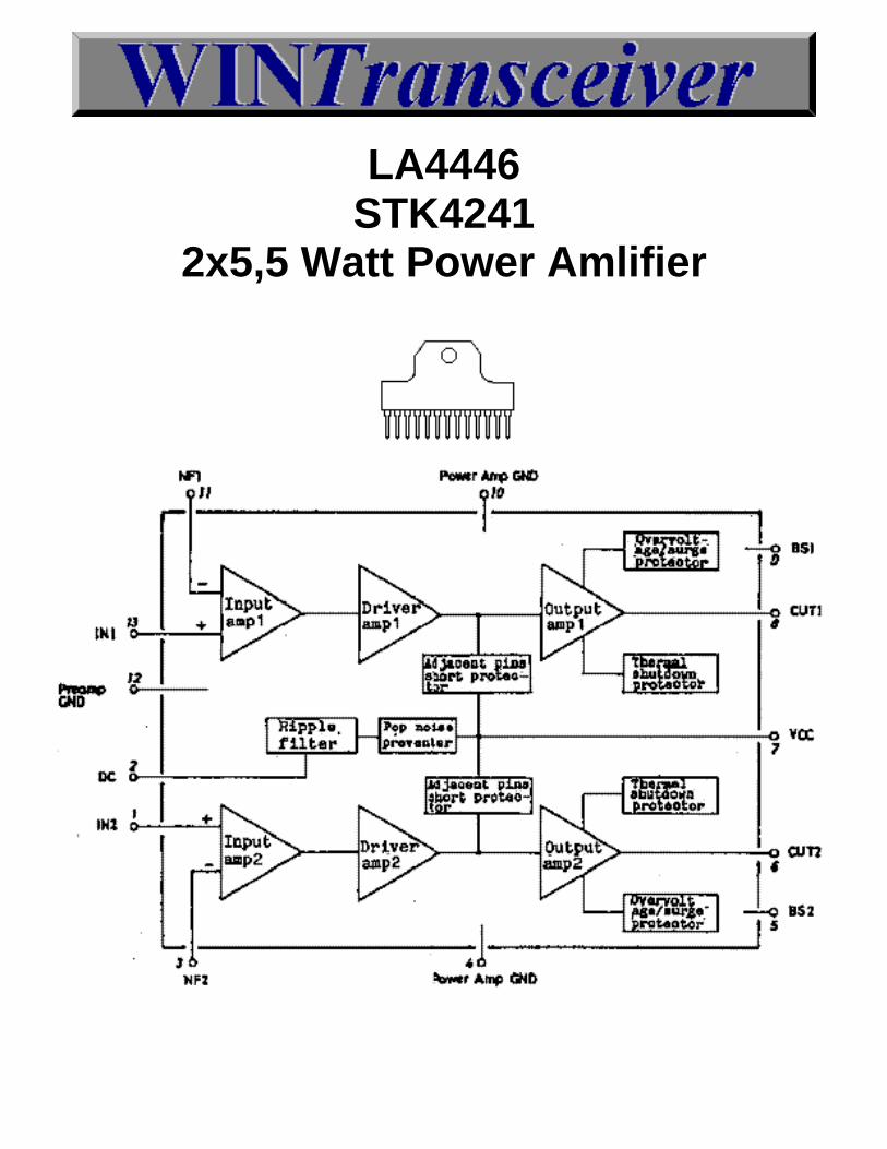
LA4446STK4241
2x5,5 Watt Power Amlifier
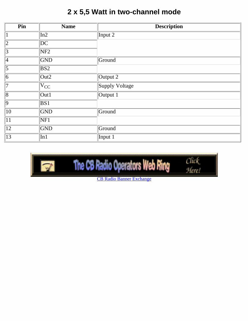
2 x 5,5 Watt in two-channel mode
Pin Name Description
1 In2 Input 2
2 DC
3 NF2
4 GND Ground
5 BS2
6 Out2 Output 2
7 VCC Supply Voltage
8 Out1 Output 1
9 BS1
10 GND Ground
11 NF1
12 GND Ground
13 In1 Input 1
CB Radio Banner Exchange
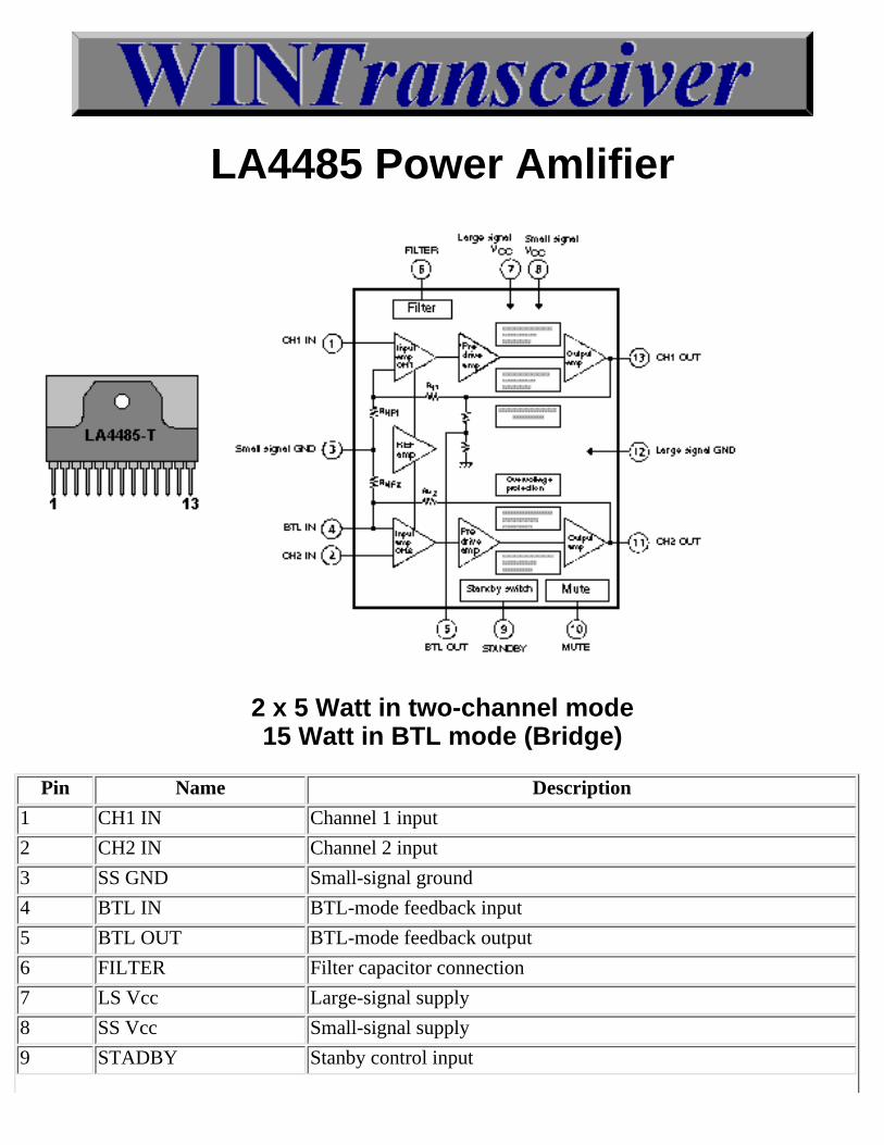
LA4485 Power Amlifier
2 x 5 Watt in two-channel mode15 Watt in BTL mode (Bridge)
Pin Name Description
1 CH1 IN Channel 1 input
2 CH2 IN Channel 2 input
3 SS GND Small-signal ground
4 BTL IN BTL-mode feedback input
5 BTL OUT BTL-mode feedback output
6 FILTER Filter capacitor connection
7 LS Vcc Large-signal supply
8 SS Vcc Small-signal supply
9 STADBY Stanby control input
10 MUTE Mute control input
11 CH2 OUT Channel 2 output
12 LS GND Large-signal ground
13 CH! OUT Channel 1 out
CB Radio Banner Exchange
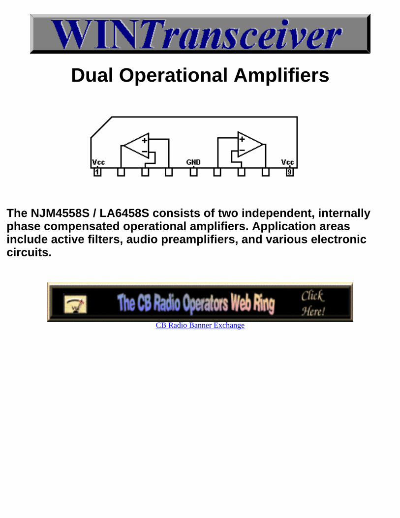
Dual Operational Amplifiers
The NJM4558S / LA6458S consists of two independent, internallyphase compensated operational amplifiers. Application areasinclude active filters, audio preamplifiers, and various electroniccircuits.
CB Radio Banner Exchange
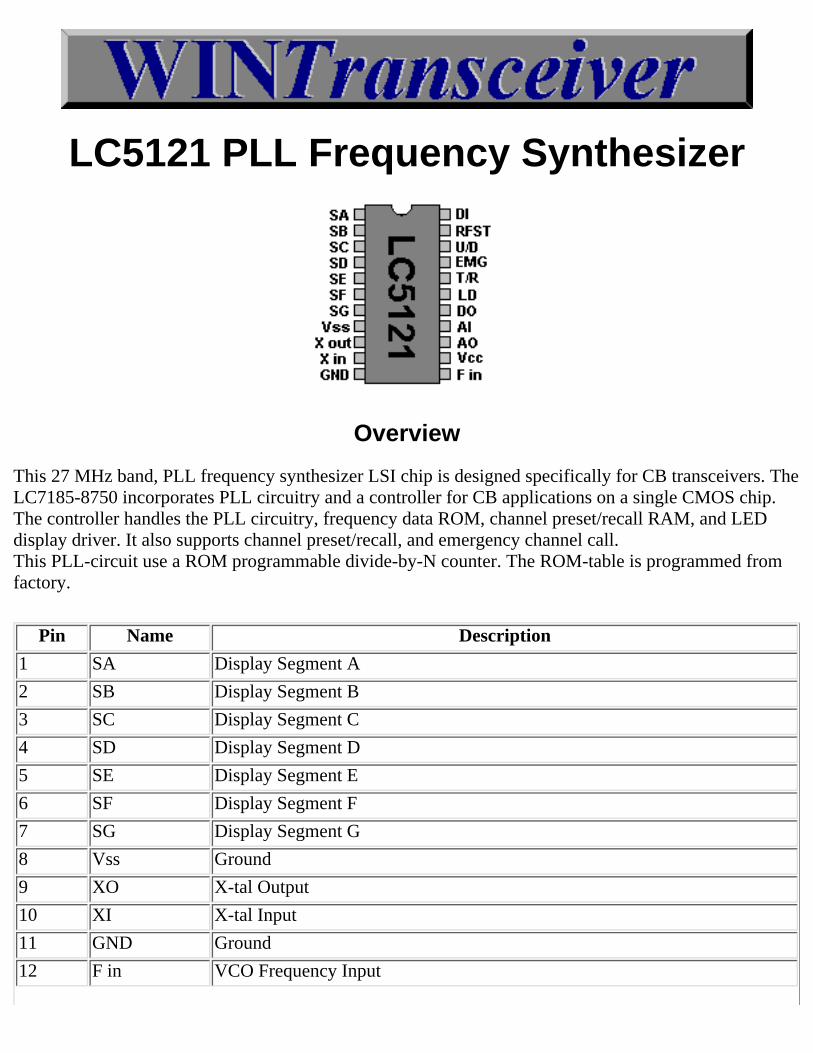
LC5121 PLL Frequency Synthesizer
Overview
This 27 MHz band, PLL frequency synthesizer LSI chip is designed specifically for CB transceivers. TheLC7185-8750 incorporates PLL circuitry and a controller for CB applications on a single CMOS chip.The controller handles the PLL circuitry, frequency data ROM, channel preset/recall RAM, and LEDdisplay driver. It also supports channel preset/recall, and emergency channel call.This PLL-circuit use a ROM programmable divide-by-N counter. The ROM-table is programmed fromfactory.
Pin Name Description
1 SA Display Segment A
2 SB Display Segment B
3 SC Display Segment C
4 SD Display Segment D
5 SE Display Segment E
6 SF Display Segment F
7 SG Display Segment G
8 Vss Ground
9 XO X-tal Output
10 XI X-tal Input
11 GND Ground
12 F in VCO Frequency Input
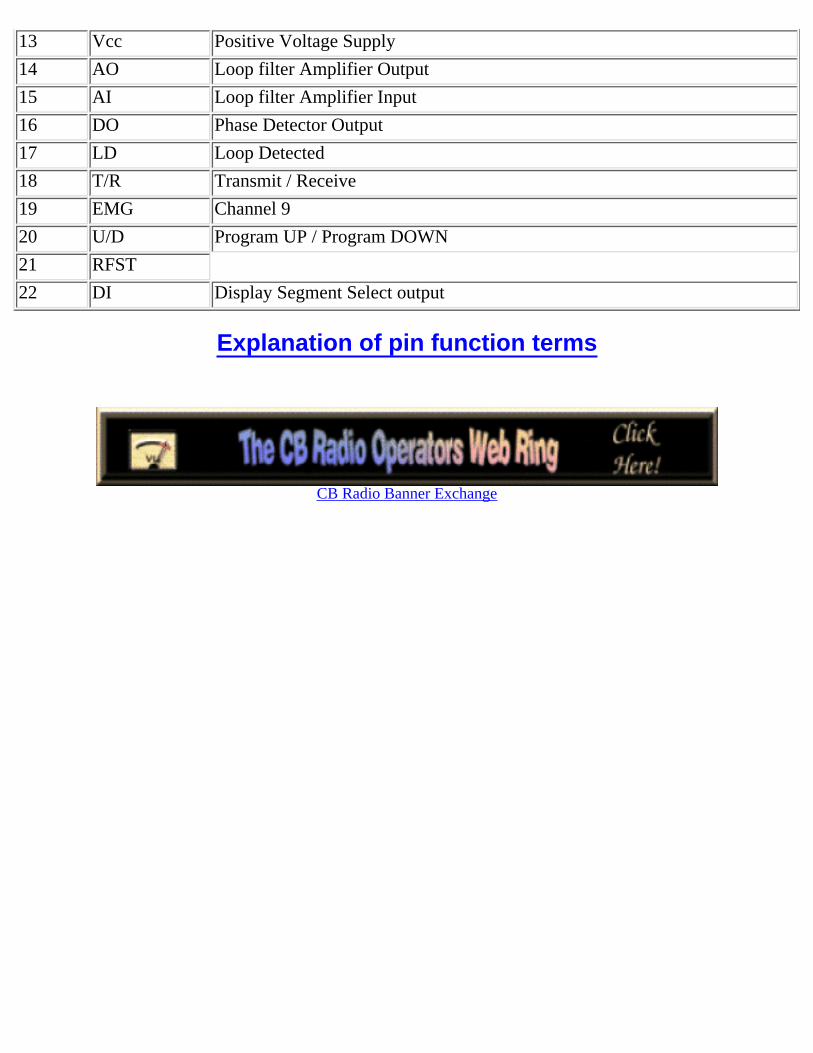
13 Vcc Positive Voltage Supply
14 AO Loop filter Amplifier Output
15 AI Loop filter Amplifier Input
16 DO Phase Detector Output
17 LD Loop Detected
18 T/R Transmit / Receive
19 EMG Channel 9
20 U/D Program UP / Program DOWN
21 RFST
22 DI Display Segment Select output
Explanation of pin function terms
CB Radio Banner Exchange
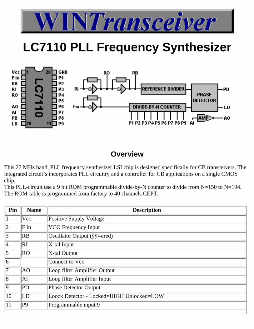
LC7110 PLL Frequency Synthesizer
Overview
This 27 MHz band, PLL frequency synthesizer LSI chip is designed specifically for CB transceivers. Theintegrated circuit`s incorporates PLL circuitry and a controller for CB applications on a single CMOSchip.This PLL-circuit use a 9 bit ROM programmable divide-by-N counter to divide from N=150 to N=194.The ROM-table is programmed from factory to 40 channels CEPT.
Pin Name Description
1 Vcc Positive Supply Voltage
2 F in VCO Frequency Input
3 RB Oscillator Output (ÿÿ\-ered)
4 RI X-tal Input
5 RO X-tal Output
6 Connect to Vcc
7 AO Loop filter Amplifier Output
8 AI Loop filter Amplifier Input
9 PD Phase Detector Output
10 LD Loock Detector - Locked=HIGH Unlocked=LOW
11 P9 Programmable input 9

12 P8 Programmable input 8
13 P7 Programmable input 7
14 P6 Programmable input 6
15 P5 Programmable input 5
16 P4 Programmable input 4
17 P3 Programmable input 3
18 P2 Programmable input 2
19 P1 Programmable input 1
20 GND Ground
Explanation of pin function terms
CB Radio Banner Exchange
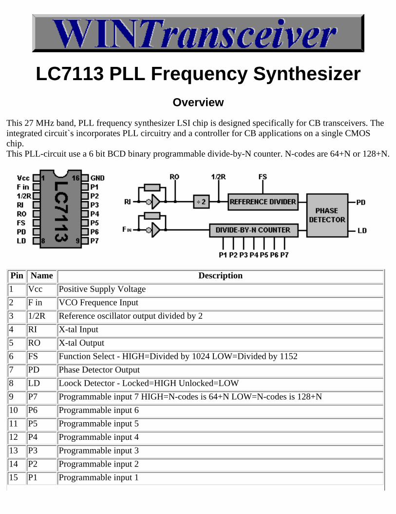
LC7113 PLL Frequency SynthesizerOverview
This 27 MHz band, PLL frequency synthesizer LSI chip is designed specifically for CB transceivers. Theintegrated circuit`s incorporates PLL circuitry and a controller for CB applications on a single CMOSchip.This PLL-circuit use a 6 bit BCD binary programmable divide-by-N counter. N-codes are 64+N or 128+N.
Pin Name Description
1 Vcc Positive Supply Voltage
2 F in VCO Frequence Input
3 1/2R Reference oscillator output divided by 2
4 RI X-tal Input
5 RO X-tal Output
6 FS Function Select - HIGH=Divided by 1024 LOW=Divided by 1152
7 PD Phase Detector Output
8 LD Loock Detector - Locked=HIGH Unlocked=LOW
9 P7 Programmable input 7 HIGH=N-codes is 64+N LOW=N-codes is 128+N
10 P6 Programmable input 6
11 P5 Programmable input 5
12 P4 Programmable input 4
13 P3 Programmable input 3
14 P2 Programmable input 2
15 P1 Programmable input 1
16 GND Ground
Explanation of pin function terms
CB Radio Banner Exchange
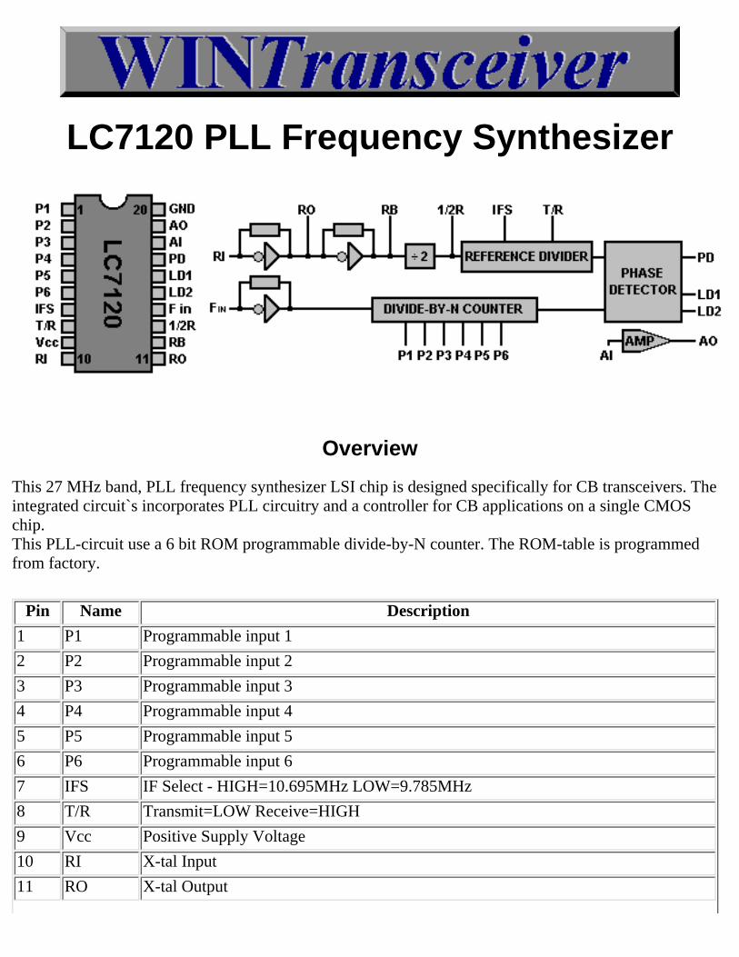
LC7120 PLL Frequency Synthesizer
Overview
This 27 MHz band, PLL frequency synthesizer LSI chip is designed specifically for CB transceivers. Theintegrated circuit`s incorporates PLL circuitry and a controller for CB applications on a single CMOSchip.This PLL-circuit use a 6 bit ROM programmable divide-by-N counter. The ROM-table is programmedfrom factory.
Pin Name Description
1 P1 Programmable input 1
2 P2 Programmable input 2
3 P3 Programmable input 3
4 P4 Programmable input 4
5 P5 Programmable input 5
6 P6 Programmable input 6
7 IFS IF Select - HIGH=10.695MHz LOW=9.785MHz
8 T/R Transmit=LOW Receive=HIGH
9 Vcc Positive Supply Voltage
10 RI X-tal Input
11 RO X-tal Output
12 RB Oscillator Output (Buffered)
13 1/2R Referency oscillator output divided by 2
14 F in VCO Frequency Input
15 LD2 Loock Detector 2
16 LD1 Loock Detector 1
17 PD Phase Detector Output
18 AI Loop filter Amplifier Input
19 AO Loop filter Amplifier Output
20 GND Ground
Explanation of pin function terms
CB Radio Banner Exchange
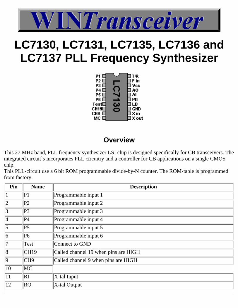
LC7130, LC7131, LC7135, LC7136 andLC7137 PLL Frequency Synthesizer
Overview
This 27 MHz band, PLL frequency synthesizer LSI chip is designed specifically for CB transceivers. Theintegrated circuit`s incorporates PLL circuitry and a controller for CB applications on a single CMOSchip.This PLL-circuit use a 6 bit ROM programmable divide-by-N counter. The ROM-table is programmedfrom factory.
Pin Name Description
1 P1 Programmable input 1
2 P2 Programmable input 2
3 P3 Programmable input 3
4 P4 Programmable input 4
5 P5 Programmable input 5
6 P6 Programmable input 6
7 Test Connect to GND
8 CH19 Called channel 19 when pins are HIGH
9 CH9 Called channel 9 when pins are HIGH
10 MC
11 RI X-tal Input
12 RO X-tal Output
13 GND Ground
14 LD Locked=HIGH Unlocked=LOW
15 PD Phase Detector Output
16 AI Loop filter Amplifier Input
17 AO Loop filter Amplifier Output
18 Vcc Positive Supply Voltage
19 F in VCO Frequency Input
20 T/R Transmit=LOW Receive=HIGH
Explanation of pin function terms
Programming Chart for LC7130/LC7131/LC7132
Channel RXDivided by
TXDivided by
1 3254 3345
2 3256 3347
.. .... ....
22 3306 3397
.. .... ....
40 3342 3433
NOTES:1. 91-count upshift on TX provides 455kHz offset for receiver IF mixing.2. Reference and Programmable Dividers use 5kHz steps.
Example of VCO Determination, Channel 1:3254 x 5kHz = 16.270MHz (RX-Mode)3345 x 5kHz = 16.725MHz (TX-Mode)
Programming Chart for LC7136/LC7137
Channel RXDivided by
TXDivided by
1 3381 2760
2 3383 2761

.. .... ....
40 3459 2799
NOTES:1. Referency and Programmable Dividers use 5kHz steps.2. TX VCO frequency is doubled to provide direct on-channel frequency.
Example of VCO Determination, Channel 1:3381 x 5kHz = 16.905MHz (RX-Mode)2760 x 5kHz = 13.800MHz (TX-Mode)(13.800MHz x 2 = 27.600MHz + 1.25kHz tuned offset = 27.60125MHz)
CB Radio Banner Exchange

LC7132 PLL Frequency Synthesizer
Overview
This 27 MHz band, PLL frequency synthesizer LSI chip is designed specifically for CB transceivers. Theintegrated circuit`s incorporates PLL circuitry and a controller for CB applications on a single CMOSchip. This PLL-circuit use a 8 bit ROM programmable divide-by-N counter. The ROM-table isprogrammed from factory.
Pin Name Description
1 P1 Programmable input 1
2 P2 Programmable input 2
3 P3 Programmable input 3
4 P4 Programmable input 4
5 P5 Programmable input 5
6 P6 Programmable input 6
7 P7 Programmable input 7
8 P8 Programmable input 8
9 CH9 Called channel 9 when pins are HIGH
10 Test Connect to GND
11 RI X-tal Input
12 RO X-tal Output
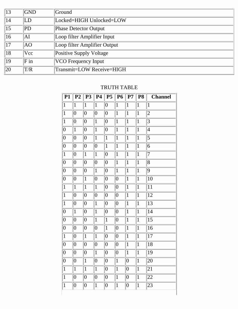
13 GND Ground
14 LD Locked=HIGH Unlocked=LOW
15 PD Phase Detector Output
16 AI Loop filter Amplifier Input
17 AO Loop filter Amplifier Output
18 Vcc Positive Supply Voltage
19 F in VCO Frequency Input
20 T/R Transmit=LOW Receive=HIGH
TRUTH TABLE
P1 P2 P3 P4 P5 P6 P7 P8 Channel
1 1 1 1 0 1 1 1 1
1 0 0 0 0 1 1 1 2
1 0 0 1 0 1 1 1 3
0 1 0 1 0 1 1 1 4
0 0 0 1 1 1 1 1 5
0 0 0 0 1 1 1 1 6
1 0 1 1 0 1 1 1 7
0 0 0 0 0 1 1 1 8
0 0 0 1 0 1 1 1 9
0 0 1 0 0 0 1 1 10
1 1 1 1 0 0 1 1 11
1 0 0 0 0 0 1 1 12
1 0 0 1 0 0 1 1 13
0 1 0 1 0 0 1 1 14
0 0 0 1 1 0 1 1 15
0 0 0 0 1 0 1 1 16
1 0 1 1 0 0 1 1 17
0 0 0 0 0 0 1 1 18
0 0 0 1 0 0 1 1 19
0 0 1 0 0 1 0 1 20
1 1 1 1 0 1 0 1 21
1 0 0 0 0 1 0 1 22
1 0 0 1 0 1 0 1 23
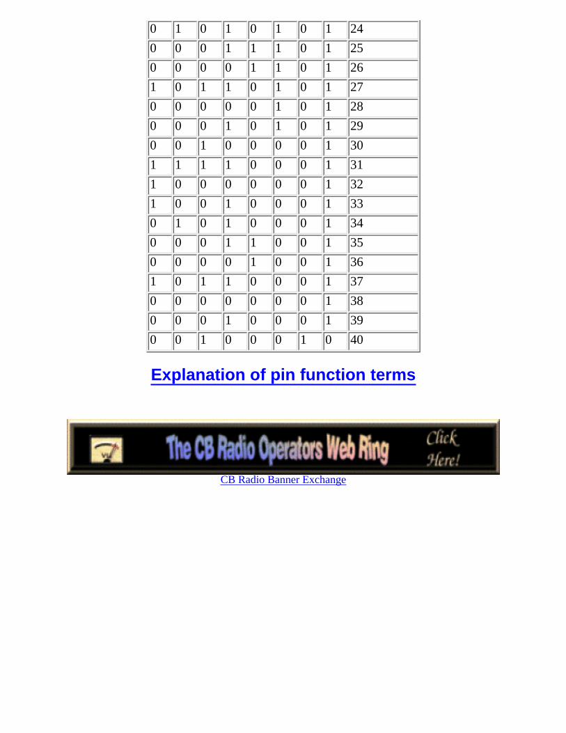
0 1 0 1 0 1 0 1 24
0 0 0 1 1 1 0 1 25
0 0 0 0 1 1 0 1 26
1 0 1 1 0 1 0 1 27
0 0 0 0 0 1 0 1 28
0 0 0 1 0 1 0 1 29
0 0 1 0 0 0 0 1 30
1 1 1 1 0 0 0 1 31
1 0 0 0 0 0 0 1 32
1 0 0 1 0 0 0 1 33
0 1 0 1 0 0 0 1 34
0 0 0 1 1 0 0 1 35
0 0 0 0 1 0 0 1 36
1 0 1 1 0 0 0 1 37
0 0 0 0 0 0 0 1 38
0 0 0 1 0 0 0 1 39
0 0 1 0 0 0 1 0 40
Explanation of pin function terms
CB Radio Banner Exchange
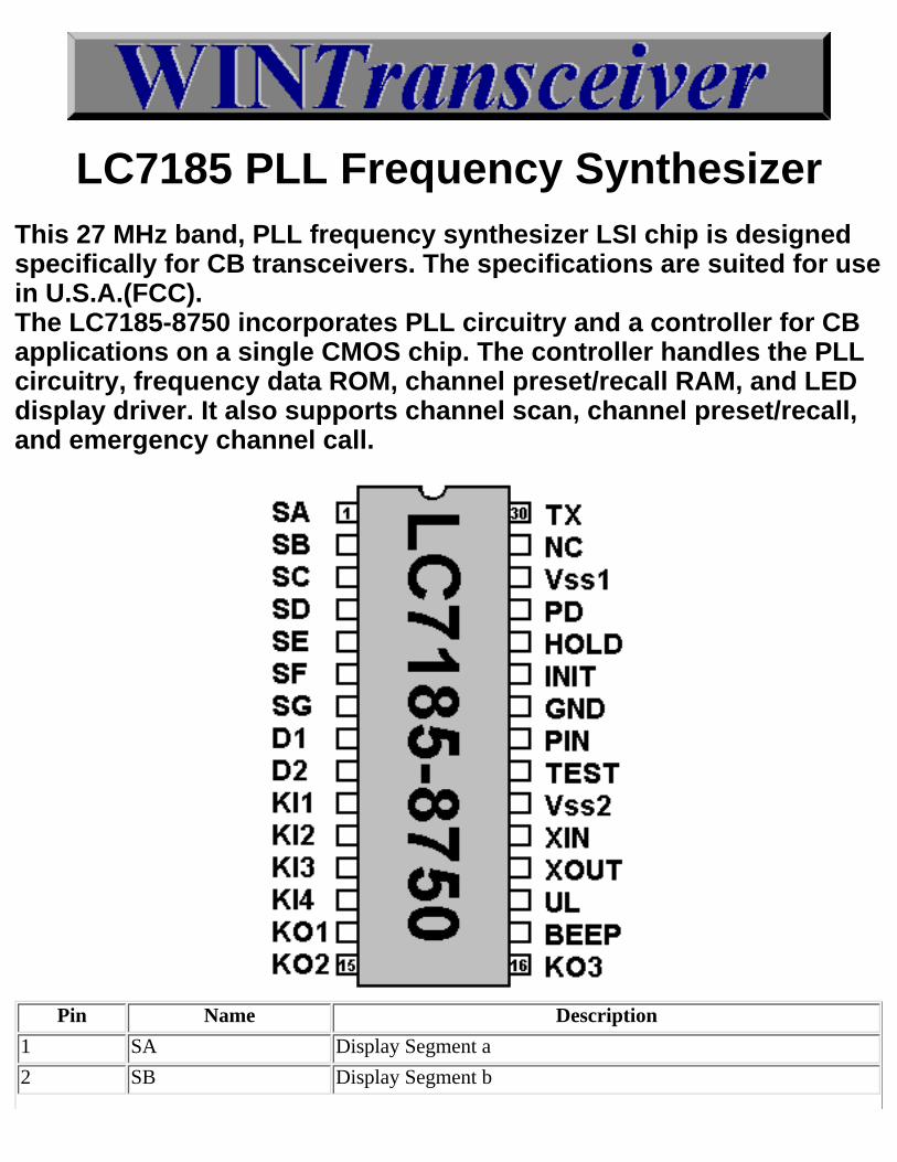
LC7185 PLL Frequency SynthesizerThis 27 MHz band, PLL frequency synthesizer LSI chip is designedspecifically for CB transceivers. The specifications are suited for usein U.S.A.(FCC).The LC7185-8750 incorporates PLL circuitry and a controller for CBapplications on a single CMOS chip. The controller handles the PLLcircuitry, frequency data ROM, channel preset/recall RAM, and LEDdisplay driver. It also supports channel scan, channel preset/recall,and emergency channel call.
Pin Name Description
1 SA Display Segment a
2 SB Display Segment b
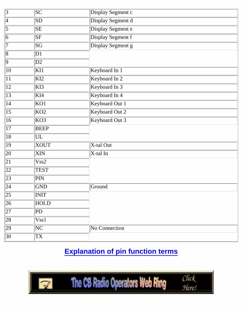
3 SC Display Segment c
4 SD Display Segment d
5 SE Display Segment e
6 SF Display Segment f
7 SG Display Segment g
8 D1
9 D2
10 KI1 Keyboard In 1
11 KI2 Keyboard In 2
12 KI3 Keyboard In 3
13 KI4 Keyboard In 4
14 KO1 Keyboard Out 1
15 KO2 Keyboard Out 2
16 KO3 Keyboard Out 3
17 BEEP
18 UL
19 XOUT X-tal Out
20 XIN X-tal In
21 Vss2
22 TEST
23 PIN
24 GND Ground
25 INIT
26 HOLD
27 PD
28 Vss1
29 NC No Connection
30 TX
Explanation of pin function terms
LC7232LC72322
Single-Chip Microcontroller with Built-InLCD Driver and PLL Circuits
OverviewThe LC7232/LC72322 is a single-chip microcontroller for use in electronic tuning applications. Itincludes on chip both LCD drivers and a PLL circuit that can operate at up to 150 MHz. It features alarge-capacity ROM, a highly efficient instruction set, and powerful hardware.
Stack: Eight levelsFast programmable dividerGeneral-purpose counters: HCTR for frequency measurement and LCTR for frequency or periodmeasurementLCD driver for displays with up to 56 segments (1/2 duty, 1/2 bias)Program memory (ROM): 4 k words by 16 bitsData memory (RAM): 256 4-bit digitsAll instructions are single-word instructionsCycle time: 2.67 µs, 13.33 µs, or 40.00 µs (option)Unlock FF: 0.55 µs detection, 1.1 µs detectionTimer FF: 1 ms, 5ms, 25ms, 125msInput ports*: One dedicated key input port and one high-breakdown voltage portOutput ports*: Two dedicated key output ports, one high-breakdown voltage open-drain port TwoCMOS output ports (of which one can be switched to be used as LCD driveroutputs) Seven CMOS output ports (mask option switchable to use as LCD ports)I/O ports*: One switchable between input and output in four-bit units and one switchable between inputand output in one-bit units Note: * Each port consists of four bits.Program runaway can be detected and a special address set (Programmable watchdog timer).Voltage detection type reset circuitOne 6-bit A/D converterTwo 8-bit D/A converters (PWM)One external interruptHold mode for RAM backupSense FF for hot/cold startup determinationPLL: 4.5 to 5.5 VCPU: 3.5 to 5.5 V
RAM: 1.3 to 5.5 V80-pin QIP
SY202General programming guidance of LC7232 devices with Seung Yong CPU SYSTEM SY202.The processors SYSTEM 202 with label Seung Yong are customized mask-programmed CPU's on baseof the LC 72322 CPU from Sanyo.Those in the following specified possibilities apply only to CPU's with the above Seung Yongdesignation and not to others! Programming are those pin 32, 33, 34, 35 of the CPU.The indicated bridges must be manufactured from the links indicated in each case to +5 Volt or GND.
Consider please:With 120 to 400 channel programming must be in the device absolutely the EMG/CH 9-Taste wired,because this becomes with many channel operation automatically the BAND selection button!
SY202 Block Diagram
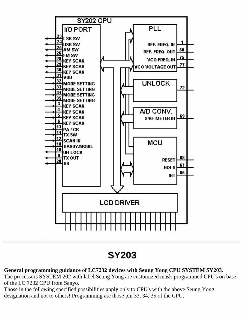
SY203General programming guidance of LC7232 devices with Seung Yong CPU SYSTEM SY203.The processors SYSTEM 202 with label Seung Yong are customized mask-programmed CPU's on baseof the LC 7232 CPU from Sanyo.Those in the following specified possibilities apply only to CPU's with the above Seung Yongdesignation and not to others! Programming are those pin 33, 34, 35 of the CPU.
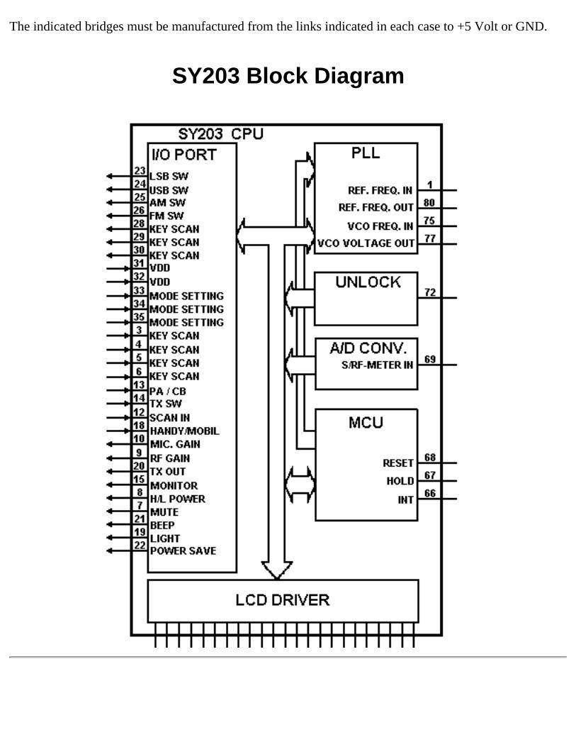
The indicated bridges must be manufactured from the links indicated in each case to +5 Volt or GND.
SY203 Block Diagram
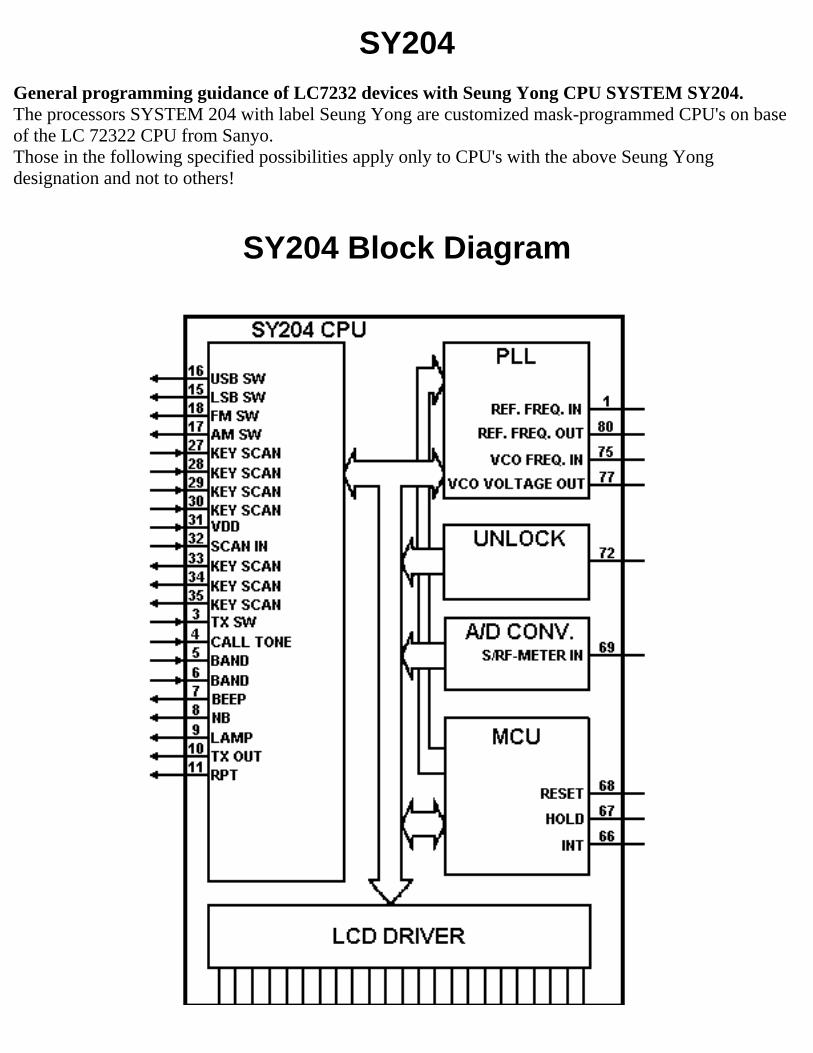
SY204General programming guidance of LC7232 devices with Seung Yong CPU SYSTEM SY204.The processors SYSTEM 204 with label Seung Yong are customized mask-programmed CPU's on baseof the LC 72322 CPU from Sanyo.Those in the following specified possibilities apply only to CPU's with the above Seung Yongdesignation and not to others!
SY204 Block Diagram

CB Radio Banner Exchange
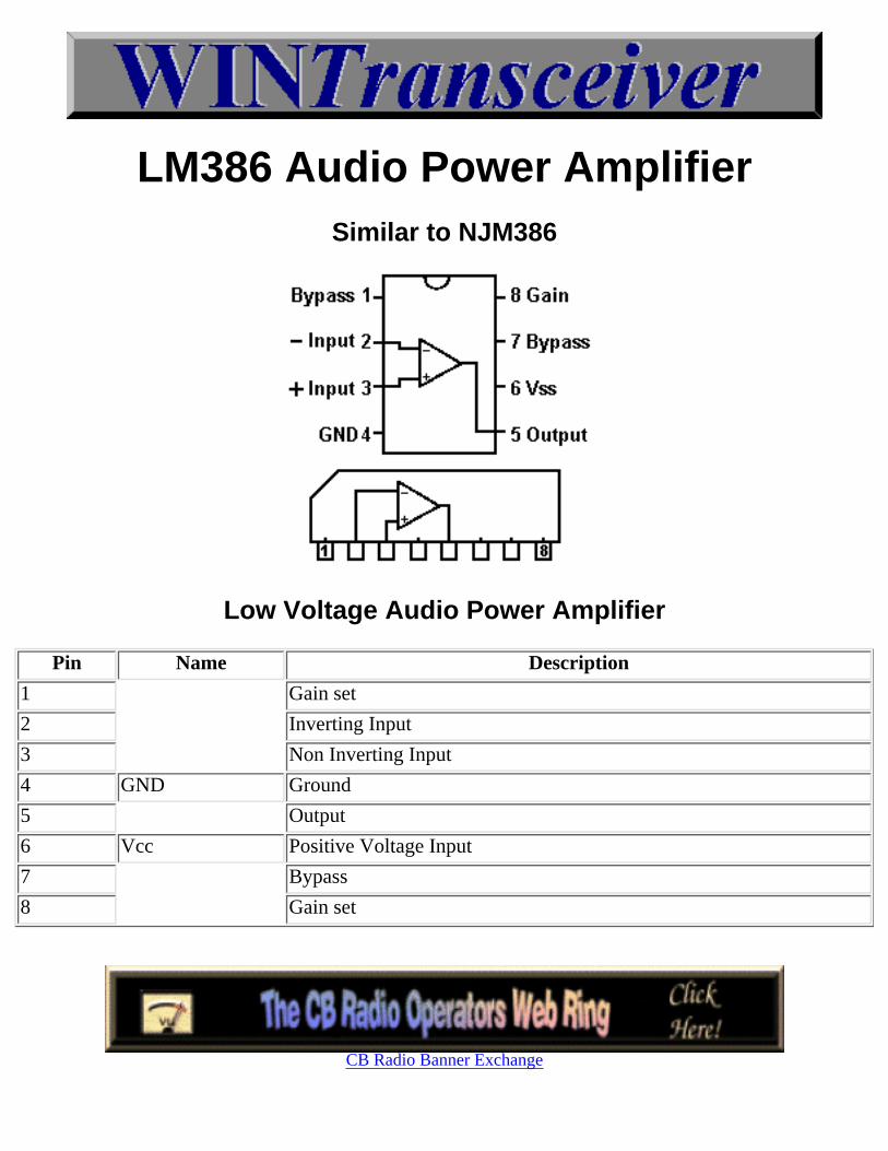
LM386 Audio Power AmplifierSimilar to NJM386
Low Voltage Audio Power Amplifier
Pin Name Description
1 Gain set
2 Inverting Input
3 Non Inverting Input
4 GND Ground
5 Output
6 Vcc Positive Voltage Input
7 Bypass
8 Gain set
CB Radio Banner Exchange

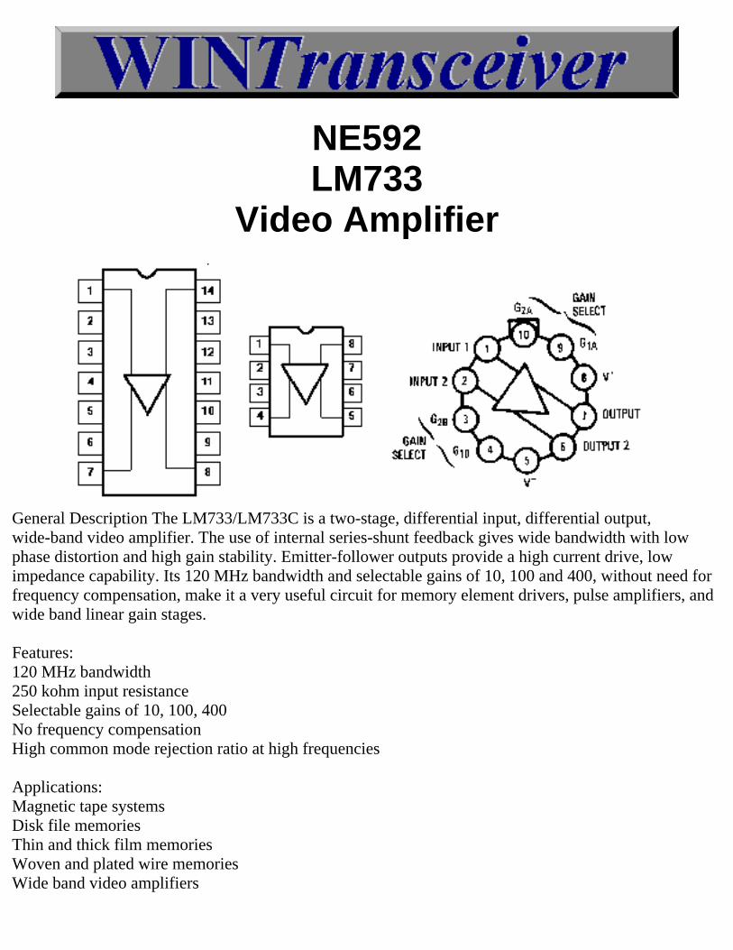
NE592LM733
Video Amplifier
General Description The LM733/LM733C is a two-stage, differential input, differential output,wide-band video amplifier. The use of internal series-shunt feedback gives wide bandwidth with lowphase distortion and high gain stability. Emitter-follower outputs provide a high current drive, lowimpedance capability. Its 120 MHz bandwidth and selectable gains of 10, 100 and 400, without need forfrequency compensation, make it a very useful circuit for memory element drivers, pulse amplifiers, andwide band linear gain stages.
Features:120 MHz bandwidth250 kohm input resistanceSelectable gains of 10, 100, 400No frequency compensationHigh common mode rejection ratio at high frequencies
Applications:Magnetic tape systemsDisk file memoriesThin and thick film memoriesWoven and plated wire memoriesWide band video amplifiers
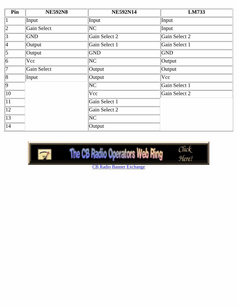
Pin NE592N8 NE592N14 LM733
1 Input Input Input
2 Gain Select NC Input
3 GND Gain Select 2 Gain Select 2
4 Output Gain Select 1 Gain Select 1
5 Output GND GND
6 Vcc NC Output
7 Gain Select Output Output
8 Input Output Vcc
9 NC Gain Select 1
10 Vcc Gain Select 2
11 Gain Select 1
12 Gain Select 2
13 NC
14 Output
CB Radio Banner Exchange
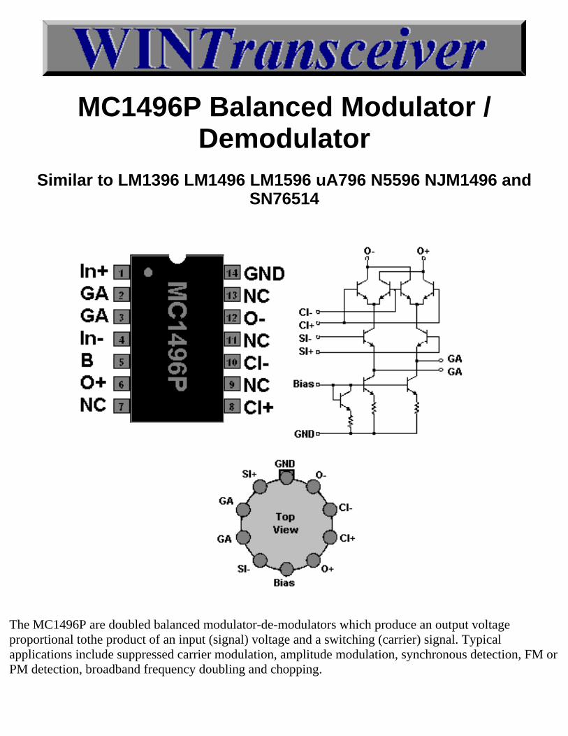
MC1496P Balanced Modulator /Demodulator
Similar to LM1396 LM1496 LM1596 uA796 N5596 NJM1496 andSN76514
The MC1496P are doubled balanced modulator-de-modulators which produce an output voltageproportional tothe product of an input (signal) voltage and a switching (carrier) signal. Typicalapplications include suppressed carrier modulation, amplitude modulation, synchronous detection, FM orPM detection, broadband frequency doubling and chopping.
- Excellent carrier suppression65 dB typical at 0.5 MHz50 dB typical at 10 MHz- Adjustable gain and signal handling- Fully balanced inputs and outputs- Low offset and drift- Wide frequency response up to 100 MHz
Pin Pin Name Description
1 1 SI+ Signal input +
2 2 GA Gain Adjust
3 3 GA Gain Adjust
4 4 SI- Signal input -
5 5 B Bias
6 6 O+ Output +
7 NC No Connection
8 7 CI+ Carrier In +
9 NC No Connection
10 8 CI- Carrier In -
11 NC No Connection
12 9 O- Output -
13 NC No Connection
14 10 GND Ground
CB Radio Banner Exchange
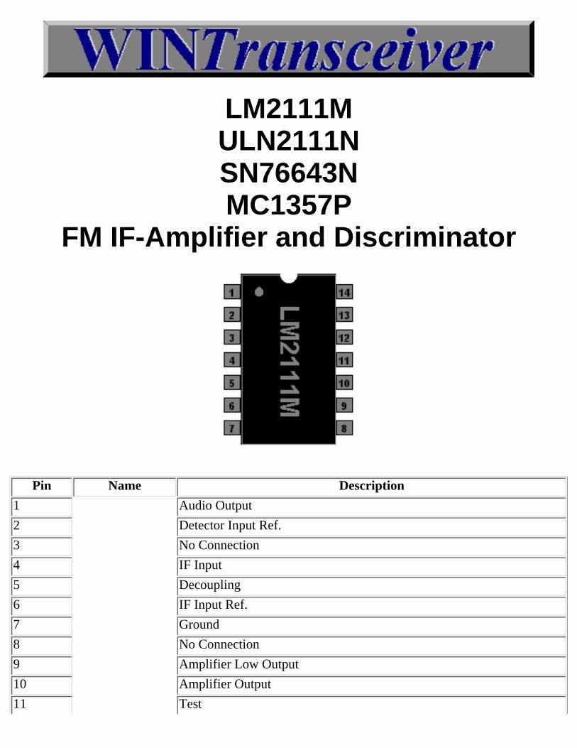
LM2111MULN2111NSN76643NMC1357P
FM IF-Amplifier and Discriminator
Pin Name Description
1 Audio Output
2 Detector Input Ref.
3 No Connection
4 IF Input
5 Decoupling
6 IF Input Ref.
7 Ground
8 No Connection
9 Amplifier Low Output
10 Amplifier Output
11 Test
12 Detector Input
13 Positive Supply Voltage
14 De-Emphasis
CB Radio Banner Exchange
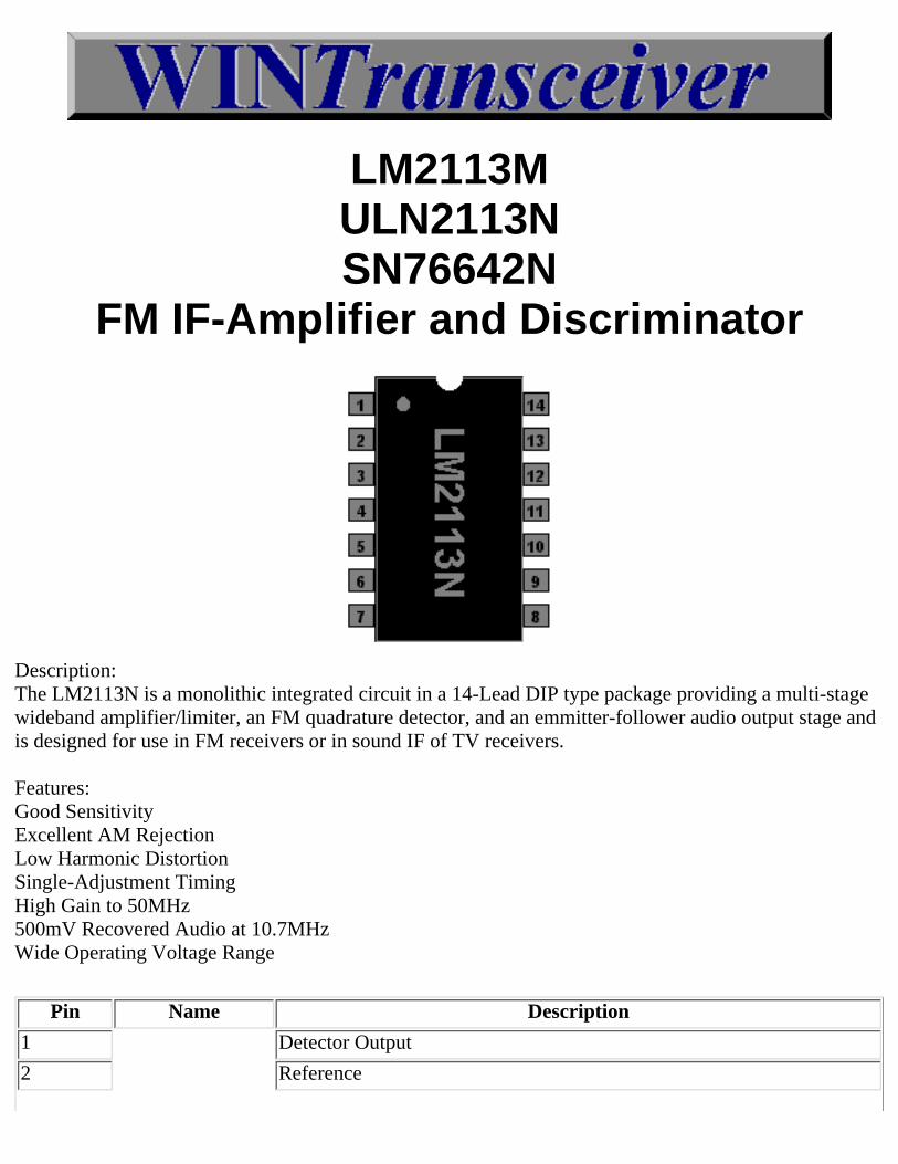
LM2113MULN2113NSN76642N
FM IF-Amplifier and Discriminator
Description:The LM2113N is a monolithic integrated circuit in a 14-Lead DIP type package providing a multi-stagewideband amplifier/limiter, an FM quadrature detector, and an emmitter-follower audio output stage andis designed for use in FM receivers or in sound IF of TV receivers.
Features:Good SensitivityExcellent AM RejectionLow Harmonic DistortionSingle-Adjustment TimingHigh Gain to 50MHz500mV Recovered Audio at 10.7MHzWide Operating Voltage Range
Pin Name Description
1 Detector Output
2 Reference
3 No Connection
4 IF Input
5 Decoupling
6 IF Input Ref.
7 Ground
8 No Connection
9 Amplifier Low Output
10 Amplifier Output
11 Test
12 Detector Input
13 Positive Supply Voltage
14 De-Emphasis
CB Radio Banner Exchange
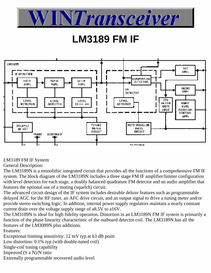
LM3189 FM IF
LM3189 FM IF SystemGeneral Description:The LM3189N is a monolithic integrated circuit that provides all the functions of a comprehensive FM IFsystem. The block diagram of the LM3189N includes a three stage FM IF amplifier/limiter configurationwith level detectors for each stage, a doubly balanced quadrature FM detector and an audio amplifier thatfeatures the optional use of a muting (squelch) circuit.The advanced circuit design of the IF system includes desirable deluxe features such as programmabledelayed AGC for the RF tuner, an AFC drive circuit, and an output signal to drive a tuning meter and/orprovide stereo switching logic. In addition, internal power supply regulators maintain a nearly constantcurrent drain over the voltage supply range of a8.5V to a16V.The LM3189N is ideal for high fidelity operation. Distortion in an LM3189N FM IF system is primarily afunction of the phase linearity characteristic of the outboard detector coil. The LM3189N has all thefeatures of the LM3089N plus additions.Features:Exceptional limiting sensitivity: 12 mV typ at b3 dB pointLow distortion: 0.1% typ (with double-tuned coil)Single-coil tuning capabilityImproved (S a N)/N ratioExternally programmable recovered audio level
Provides specific signal for control of inter-channel muting (squelch)Provides specific signal for direct drive of a tuning meterOn channel step for search controlProvides programmable AGC voltage for RF amplifierProvides a specific circuit for flexible audio outputInternal supply voltage regulatorsExternally programmable ON channel step width, and deviation at which muting occurs
Pin Name Description
1 IF Input
2 IF In Bypass
3 IF In Bypass
4 Frame
5 Mute Control
6 Audio Output
7 AFC Output
8 IF Output
9 Quad Input
10 Ref Bias
11 Vcc Positive Supply Voltage
12 Mute Logic
13 Tune Meter
14 GND Ground
15 Delayed AGC
16 AGC
CB Radio Banner Exchange
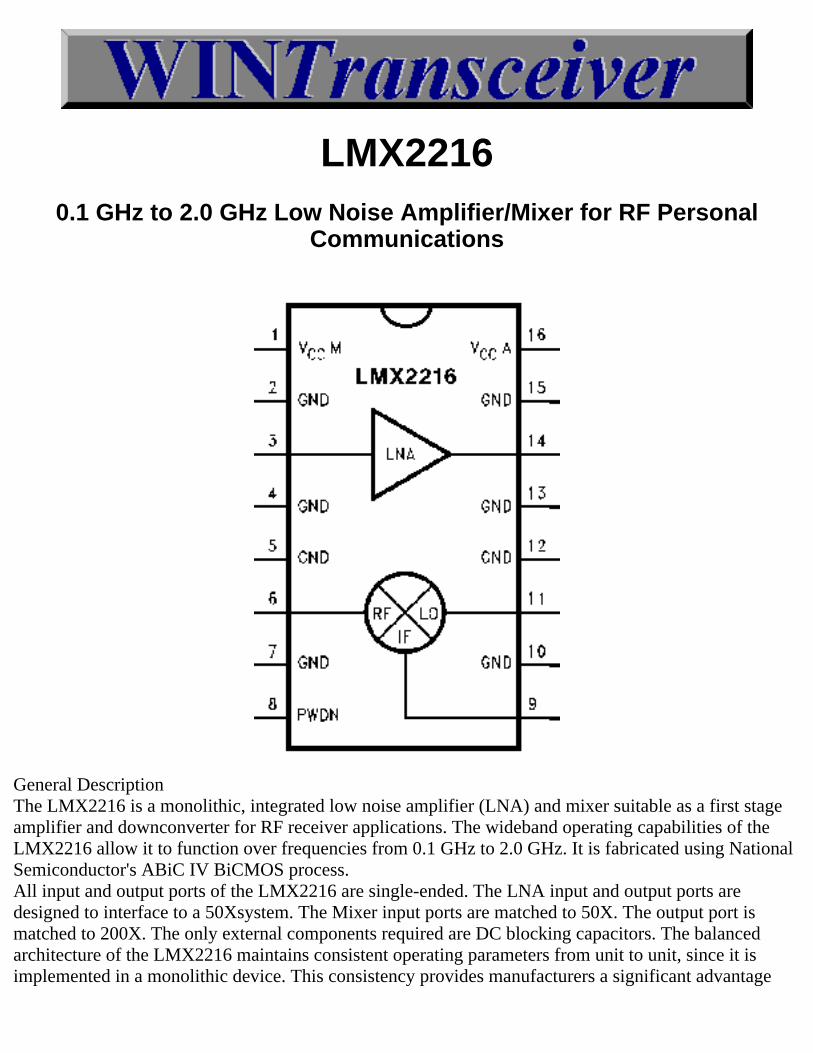
LMX22160.1 GHz to 2.0 GHz Low Noise Amplifier/Mixer for RF Personal
Communications
General DescriptionThe LMX2216 is a monolithic, integrated low noise amplifier (LNA) and mixer suitable as a first stageamplifier and downconverter for RF receiver applications. The wideband operating capabilities of theLMX2216 allow it to function over frequencies from 0.1 GHz to 2.0 GHz. It is fabricated using NationalSemiconductor's ABiC IV BiCMOS process.All input and output ports of the LMX2216 are single-ended. The LNA input and output ports aredesigned to interface to a 50Xsystem. The Mixer input ports are matched to 50X. The output port ismatched to 200X. The only external components required are DC blocking capacitors. The balancedarchitecture of the LMX2216 maintains consistent operating parameters from unit to unit, since it isimplemented in a monolithic device. This consistency provides manufacturers a significant advantage
since tuning procedures often needed with discrete designsÐcan be reduced or eliminated.The low noise amplifier produces very flat gain over the entire operating range. The doubly-balanced,Gilbert-cell mixer provides good LO-RF isolation and cancellation of second order distortion products. Apower down feature is implemented on the LMX2216 that is especially useful for standby operationcommon in Time Division Multiple Access (TDMA) and Time Division Duplex (TDD) systems.The LMX2216 is available in a narrow-body 16-pin surface mount plastic package.
Features :Wideband RF operation from 0.1 GHz to 2.0 GHzNo external biasing components necessary3V operationLNA input and output ports matched to 50XMixer input ports matched to 50X, output port matched to 200X.Doubly balanced Gilbert cell mixer (single ended input and output)Low power consumptionPower down featureSmall outline, plastic surface mount package
Applications :Digital European Cordless Telecommunications (DECT)Portable wireless communications (PCS/PCN, cordless)Wireless local area networks (WLANs)Digital cellular telephone systemsOther wireless communications systems
CB Radio Banner Exchange
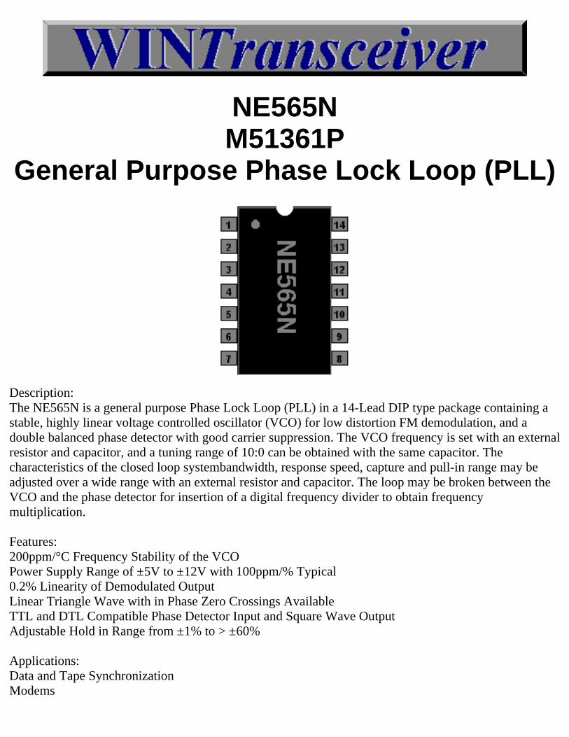
NE565NM51361P
General Purpose Phase Lock Loop (PLL)
Description:The NE565N is a general purpose Phase Lock Loop (PLL) in a 14-Lead DIP type package containing astable, highly linear voltage controlled oscillator (VCO) for low distortion FM demodulation, and adouble balanced phase detector with good carrier suppression. The VCO frequency is set with an externalresistor and capacitor, and a tuning range of 10:0 can be obtained with the same capacitor. Thecharacteristics of the closed loop systembandwidth, response speed, capture and pull-in range may beadjusted over a wide range with an external resistor and capacitor. The loop may be broken between theVCO and the phase detector for insertion of a digital frequency divider to obtain frequencymultiplication.
Features:200ppm/°C Frequency Stability of the VCOPower Supply Range of ±5V to ±12V with 100ppm/% Typical0.2% Linearity of Demodulated OutputLinear Triangle Wave with in Phase Zero Crossings AvailableTTL and DTL Compatible Phase Detector Input and Square Wave OutputAdjustable Hold in Range from ±1% to > ±60%
Applications:Data and Tape SynchronizationModems
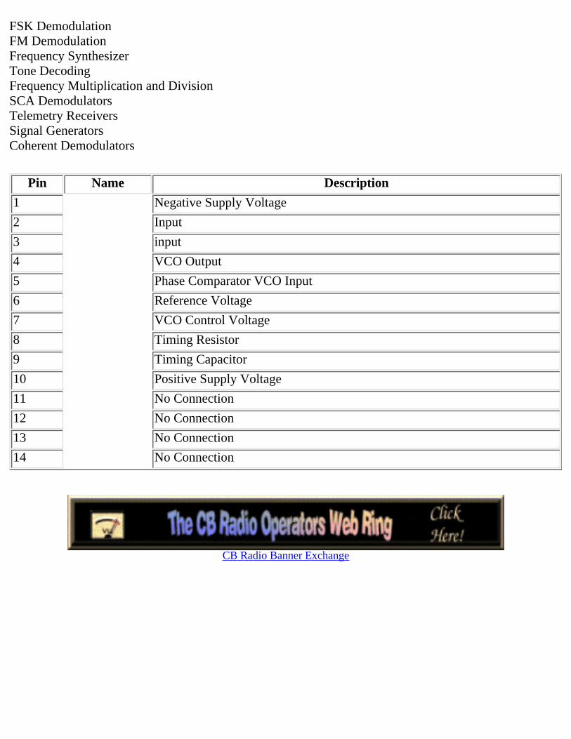
FSK DemodulationFM DemodulationFrequency SynthesizerTone DecodingFrequency Multiplication and DivisionSCA DemodulatorsTelemetry ReceiversSignal GeneratorsCoherent Demodulators
Pin Name Description
1 Negative Supply Voltage
2 Input
3 input
4 VCO Output
5 Phase Comparator VCO Input
6 Reference Voltage
7 VCO Control Voltage
8 Timing Resistor
9 Timing Capacitor
10 Positive Supply Voltage
11 No Connection
12 No Connection
13 No Connection
14 No Connection
CB Radio Banner Exchange
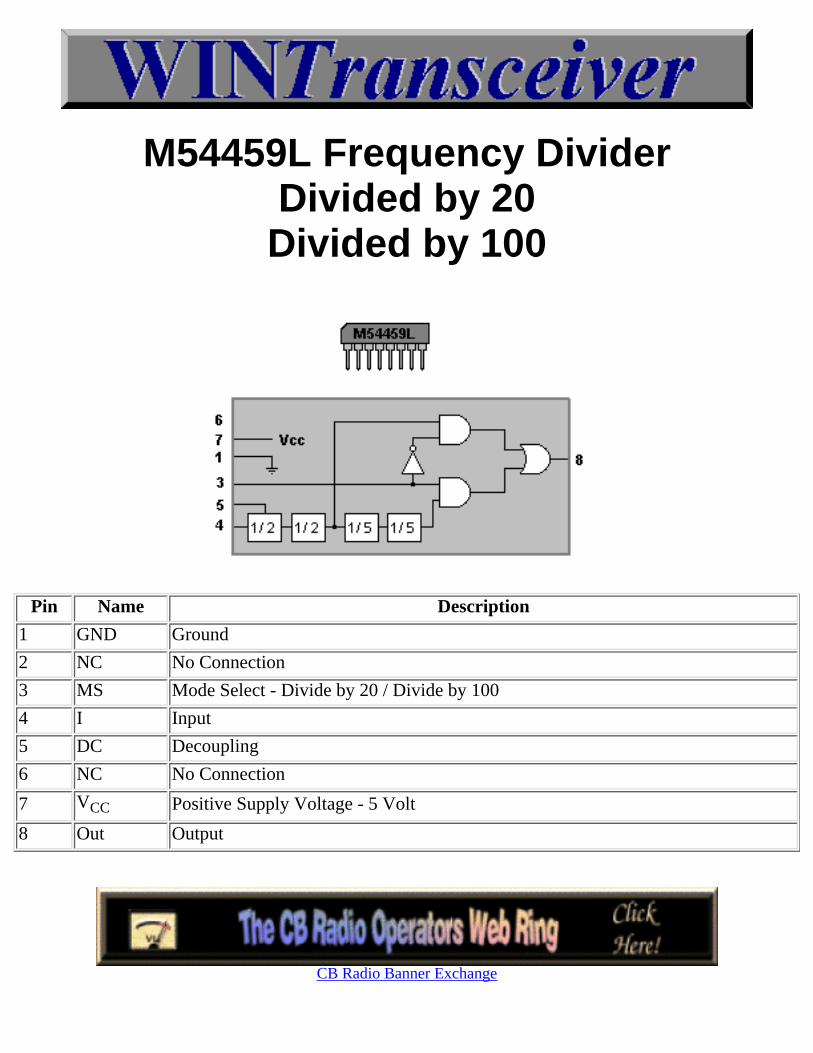
M54459L Frequency DividerDivided by 20Divided by 100
Pin Name Description
1 GND Ground
2 NC No Connection
3 MS Mode Select - Divide by 20 / Divide by 100
4 I Input
5 DC Decoupling
6 NC No Connection
7 VCC Positive Supply Voltage - 5 Volt
8 Out Output
CB Radio Banner Exchange

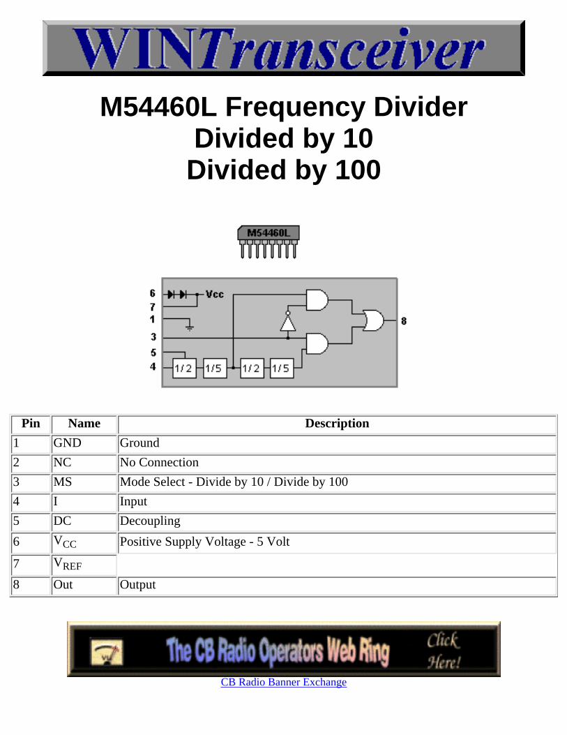
M54460L Frequency DividerDivided by 10Divided by 100
Pin Name Description
1 GND Ground
2 NC No Connection
3 MS Mode Select - Divide by 10 / Divide by 100
4 I Input
5 DC Decoupling
6 VCC Positive Supply Voltage - 5 Volt
7 VREF
8 Out Output
CB Radio Banner Exchange

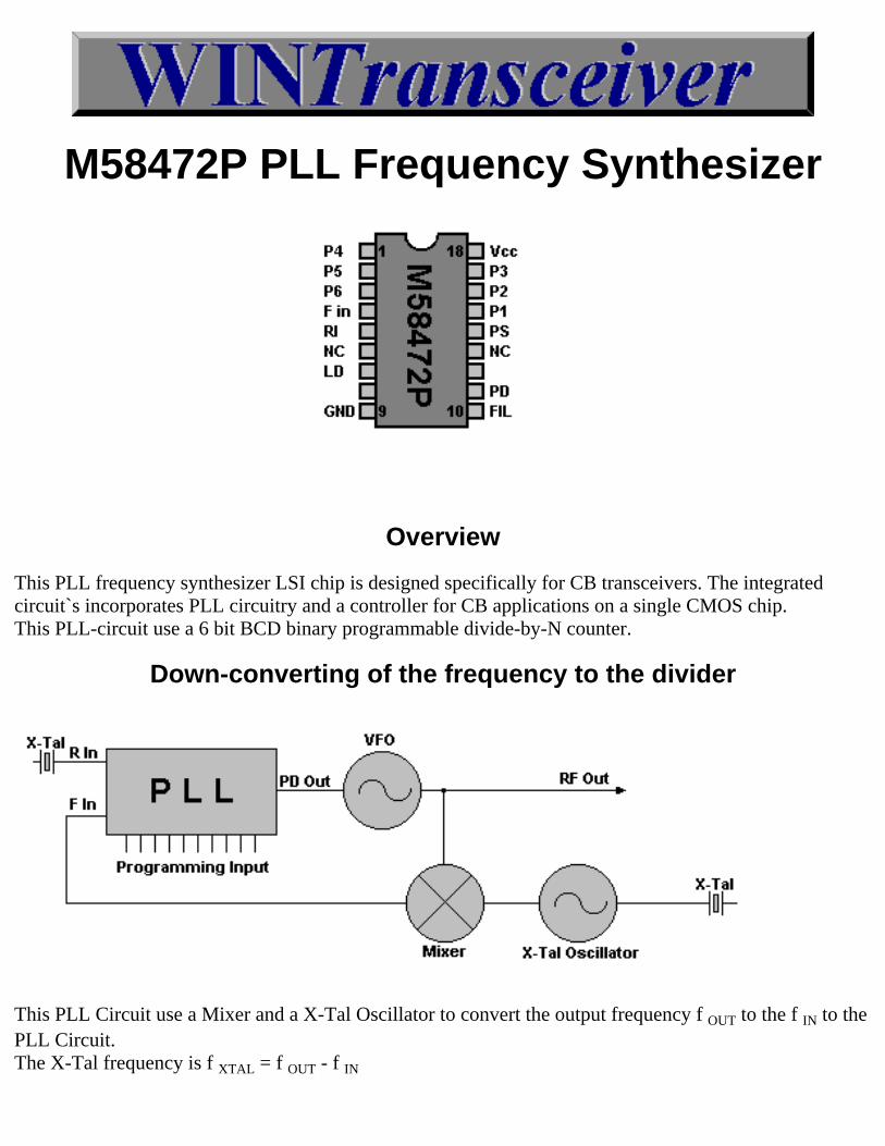
M58472P PLL Frequency Synthesizer
Overview
This PLL frequency synthesizer LSI chip is designed specifically for CB transceivers. The integratedcircuit`s incorporates PLL circuitry and a controller for CB applications on a single CMOS chip.This PLL-circuit use a 6 bit BCD binary programmable divide-by-N counter.
Down-converting of the frequency to the divider
This PLL Circuit use a Mixer and a X-Tal Oscillator to convert the output frequency f OUT to the f IN to thePLL Circuit.The X-Tal frequency is f XTAL = f OUT - f IN
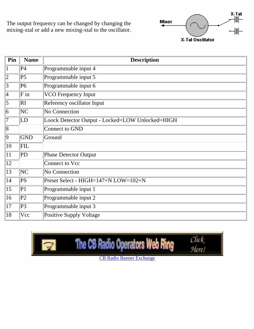
The output frequency can be changed by changing themixing-xtal or add a new mixing-xtal to the oscillator.
Pin Name Description
1 P4 Programmable input 4
2 P5 Programmable input 5
3 P6 Programmable input 6
4 F in VCO Frequency Input
5 RI Referency oscillator Input
6 NC No Connection
7 LD Loock Detector Output - Locked=LOW Unlocked=HIGH
8 Connect to GND
9 GND Ground
10 FIL
11 PD Phase Detector Output
12 Connect to Vcc
13 NC No Connection
14 PS Preset Select - HIGH=147+N LOW=102+N
15 P1 Programmable input 1
16 P2 Programmable input 2
17 P3 Programmable input 3
18 Vcc Positive Supply Voltage
CB Radio Banner Exchange
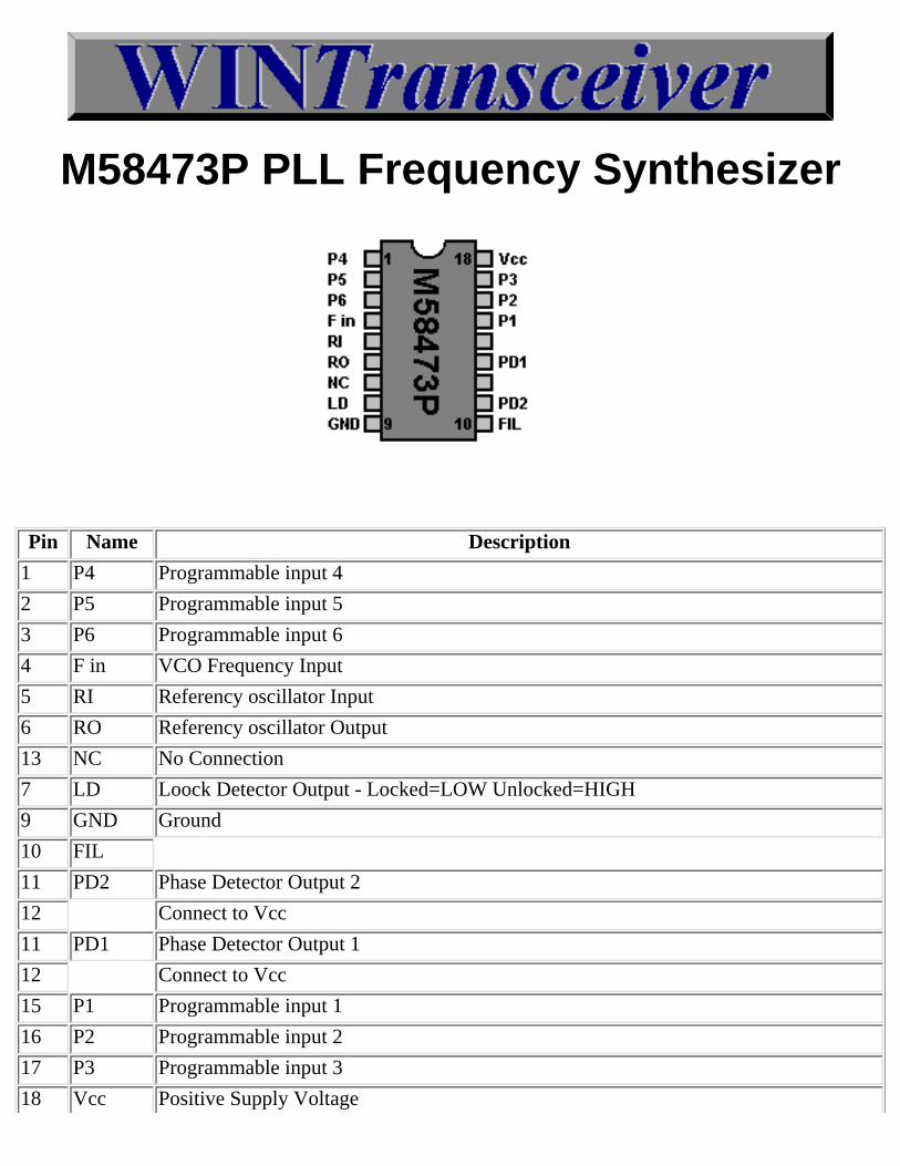
M58473P PLL Frequency Synthesizer
Pin Name Description
1 P4 Programmable input 4
2 P5 Programmable input 5
3 P6 Programmable input 6
4 F in VCO Frequency Input
5 RI Referency oscillator Input
6 RO Referency oscillator Output
13 NC No Connection
7 LD Loock Detector Output - Locked=LOW Unlocked=HIGH
9 GND Ground
10 FIL
11 PD2 Phase Detector Output 2
12 Connect to Vcc
11 PD1 Phase Detector Output 1
12 Connect to Vcc
15 P1 Programmable input 1
16 P2 Programmable input 2
17 P3 Programmable input 3
18 Vcc Positive Supply Voltage

CB Radio Banner Exchange
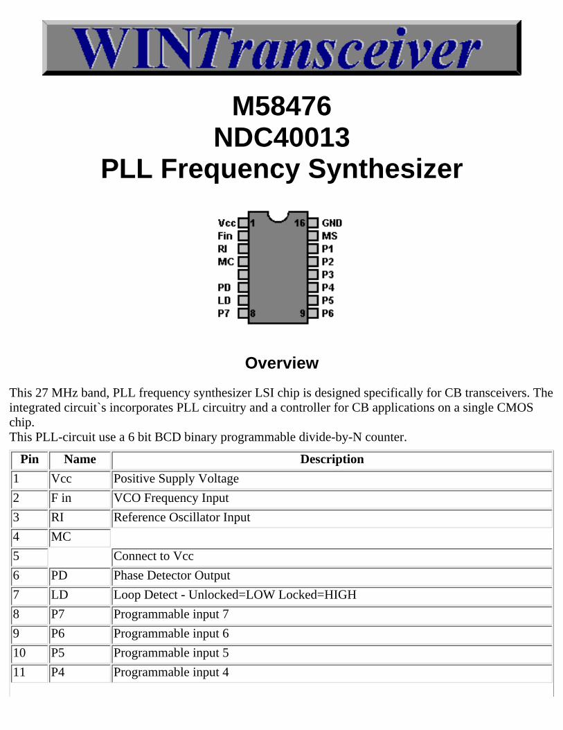
M58476NDC40013
PLL Frequency Synthesizer
Overview
This 27 MHz band, PLL frequency synthesizer LSI chip is designed specifically for CB transceivers. Theintegrated circuit`s incorporates PLL circuitry and a controller for CB applications on a single CMOSchip.This PLL-circuit use a 6 bit BCD binary programmable divide-by-N counter.
Pin Name Description
1 Vcc Positive Supply Voltage
2 F in VCO Frequency Input
3 RI Reference Oscillator Input
4 MC
5 Connect to Vcc
6 PD Phase Detector Output
7 LD Loop Detect - Unlocked=LOW Locked=HIGH
8 P7 Programmable input 7
9 P6 Programmable input 6
10 P5 Programmable input 5
11 P4 Programmable input 4

12 P3 Programmable input 3
13 P2 Programmable input 2
14 P1 Programmable input 1
15 MS Mode Select - HIGH=10kHz LOW=5kHz
16 GND Ground
CB Radio Banner Exchange
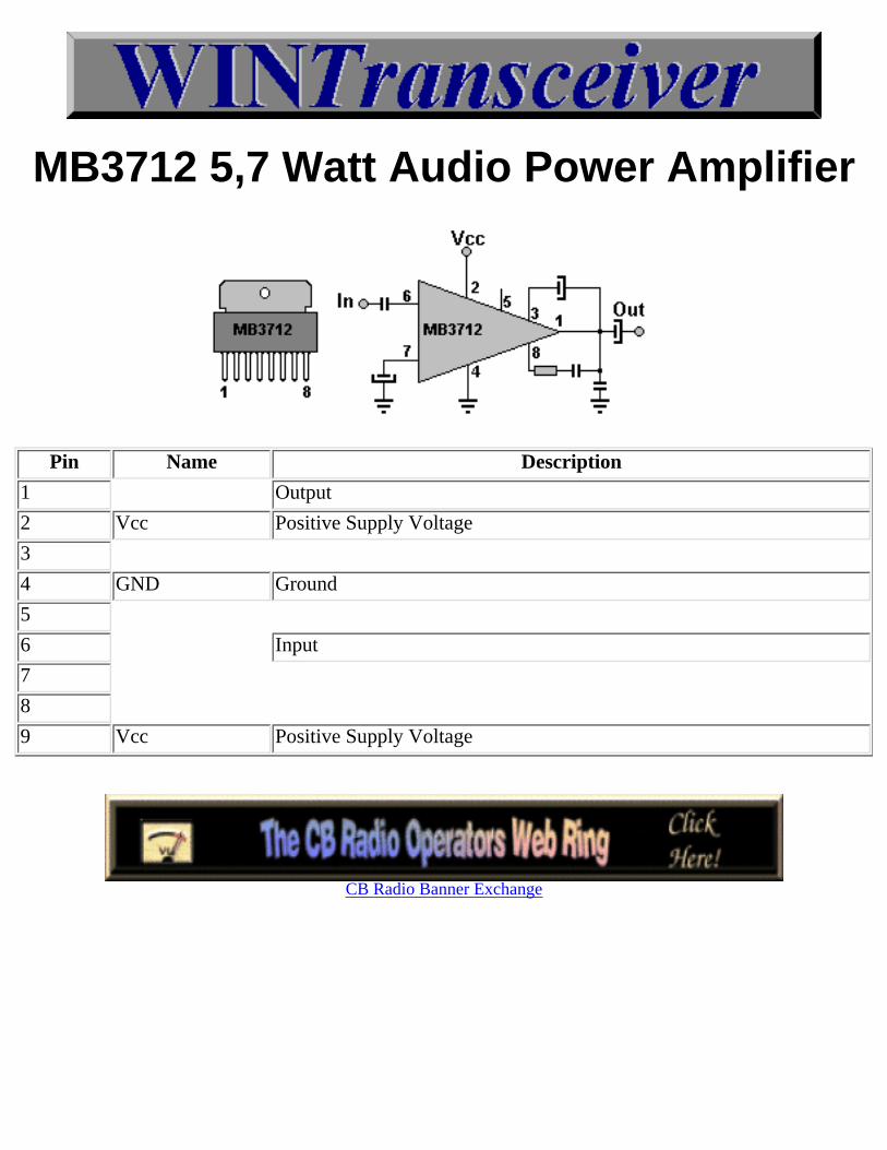
MB3712 5,7 Watt Audio Power Amplifier
Pin Name Description
1 Output
2 Vcc Positive Supply Voltage
3
4 GND Ground
5
6 Input
7
8
9 Vcc Positive Supply Voltage
CB Radio Banner Exchange
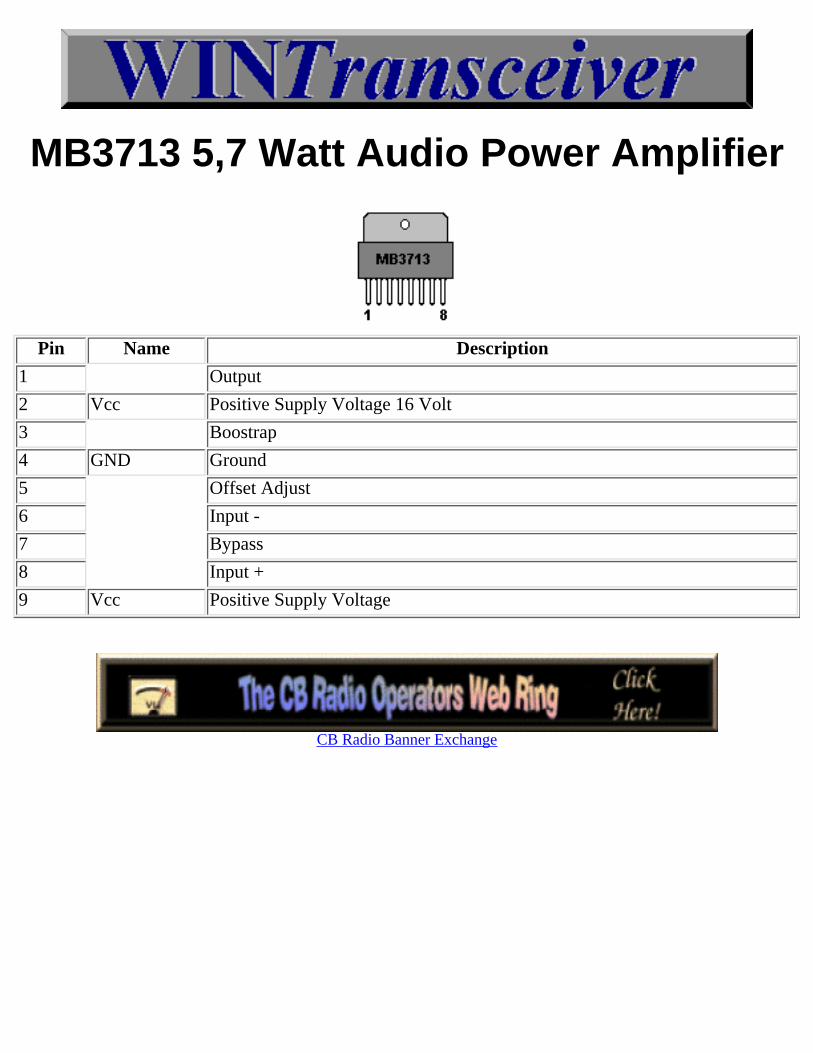
MB3713 5,7 Watt Audio Power Amplifier
Pin Name Description
1 Output
2 Vcc Positive Supply Voltage 16 Volt
3 Boostrap
4 GND Ground
5 Offset Adjust
6 Input -
7 Bypass
8 Input +
9 Vcc Positive Supply Voltage
CB Radio Banner Exchange
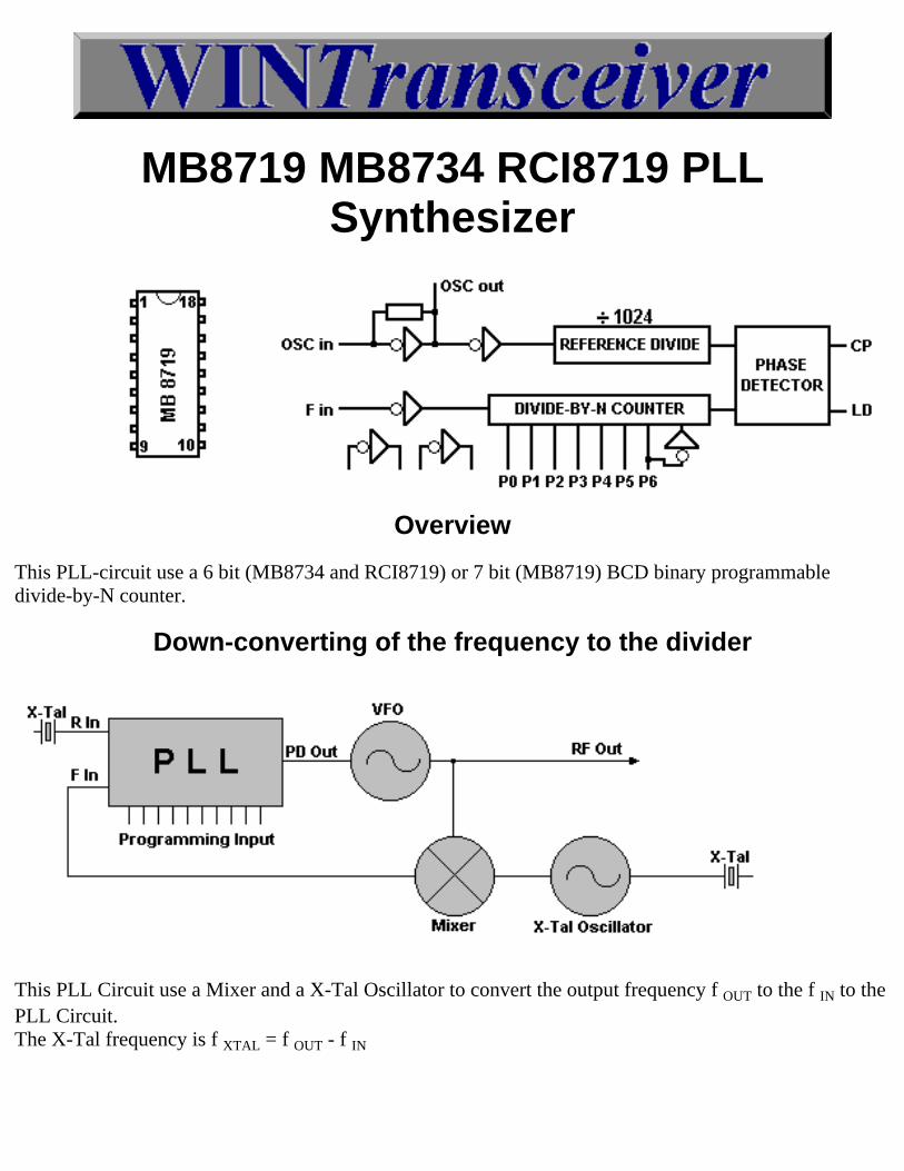
MB8719 MB8734 RCI8719 PLLSynthesizer
Overview
This PLL-circuit use a 6 bit (MB8734 and RCI8719) or 7 bit (MB8719) BCD binary programmabledivide-by-N counter.
Down-converting of the frequency to the divider
This PLL Circuit use a Mixer and a X-Tal Oscillator to convert the output frequency f OUT to the f IN to thePLL Circuit.The X-Tal frequency is f XTAL = f OUT - f IN
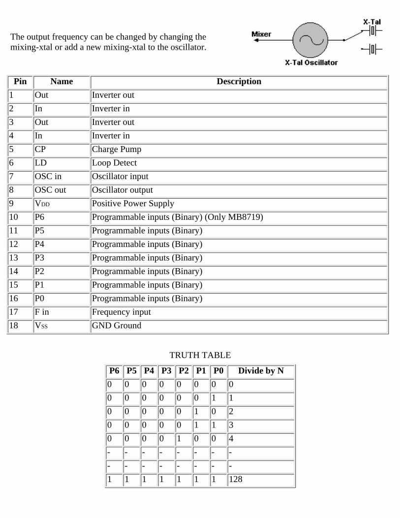
The output frequency can be changed by changing themixing-xtal or add a new mixing-xtal to the oscillator.
Pin Name Description
1 Out Inverter out
2 In Inverter in
3 Out Inverter out
4 In Inverter in
5 CP Charge Pump
6 LD Loop Detect
7 OSC in Oscillator input
8 OSC out Oscillator output
9 VDD Positive Power Supply
10 P6 Programmable inputs (Binary) (Only MB8719)
11 P5 Programmable inputs (Binary)
12 P4 Programmable inputs (Binary)
13 P3 Programmable inputs (Binary)
14 P2 Programmable inputs (Binary)
15 P1 Programmable inputs (Binary)
16 P0 Programmable inputs (Binary)
17 F in Frequency input
18 VSS GND Ground
TRUTH TABLE
P6 P5 P4 P3 P2 P1 P0 Divide by N
0 0 0 0 0 0 0 0
0 0 0 0 0 0 1 1
0 0 0 0 0 1 0 2
0 0 0 0 0 1 1 3
0 0 0 0 1 0 0 4
- - - - - - - -
- - - - - - - -
1 1 1 1 1 1 1 128

Explanation of pin function terms
Uniden AM/FM/SSB Chassis
CB Radio Banner Exchange
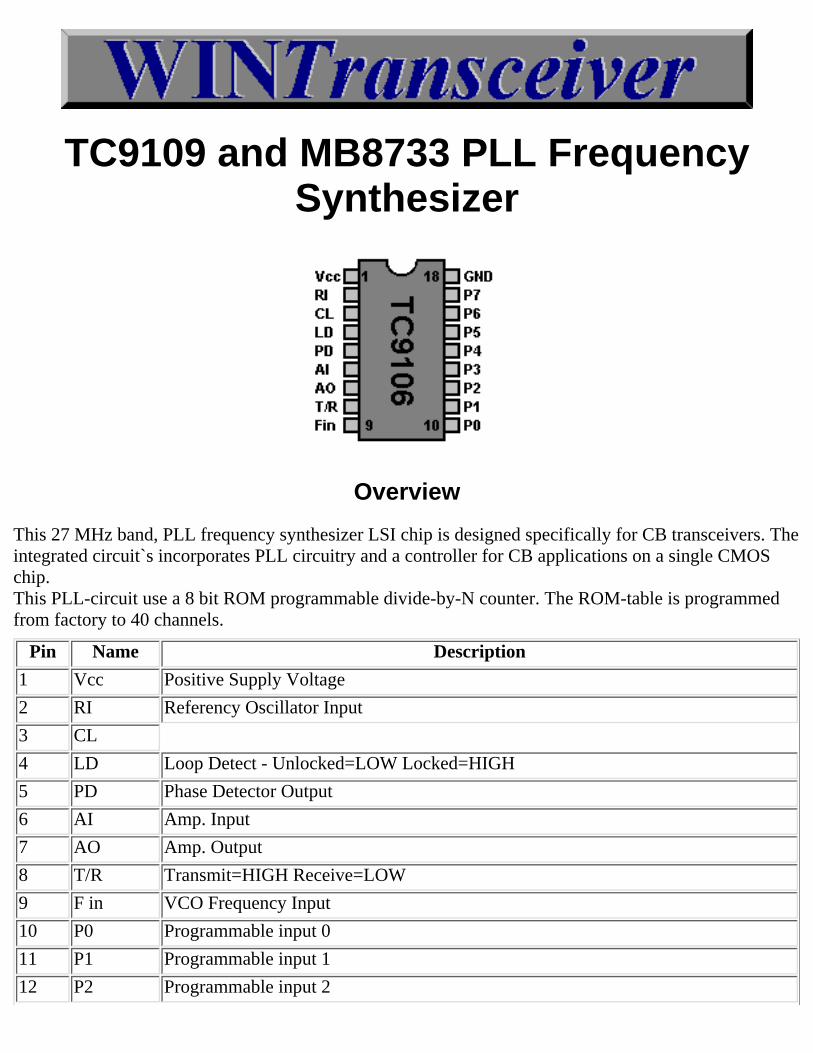
TC9109 and MB8733 PLL FrequencySynthesizer
Overview
This 27 MHz band, PLL frequency synthesizer LSI chip is designed specifically for CB transceivers. Theintegrated circuit`s incorporates PLL circuitry and a controller for CB applications on a single CMOSchip.This PLL-circuit use a 8 bit ROM programmable divide-by-N counter. The ROM-table is programmedfrom factory to 40 channels.
Pin Name Description
1 Vcc Positive Supply Voltage
2 RI Referency Oscillator Input
3 CL
4 LD Loop Detect - Unlocked=LOW Locked=HIGH
5 PD Phase Detector Output
6 AI Amp. Input
7 AO Amp. Output
8 T/R Transmit=HIGH Receive=LOW
9 F in VCO Frequency Input
10 P0 Programmable input 0
11 P1 Programmable input 1
12 P2 Programmable input 2
13 P3 Programmable input 3
14 P4 Programmable input 4
15 P5 Programmable input 5
16 P6 Programmable input 6
17 P7 Programmable input 7
18 GND Ground
Explanation of pin function terms
Programming Chart for TC9106
Channel RXDivided by
TXDivided by
1 3254 5393
2 3256 5395
.. .... ....
40 3342 5481
NOTES:1. Spesial divided by 2 circuit in TX mode change Referency Divider output to 2.5kHz steps. The 2139count upshifts produces a 13MHz VCO witch is then doubled for the direct on-channel TX-frequency.
Example of VCO Determination, Channel 1:3254 x 5kHz = 16.270MHz (RX-Mode)5393 x 2.5kHz = 134825MHz (TX-Mode)(13.4825MHz x 2 = 26.965MHz)
CB Radio Banner Exchange
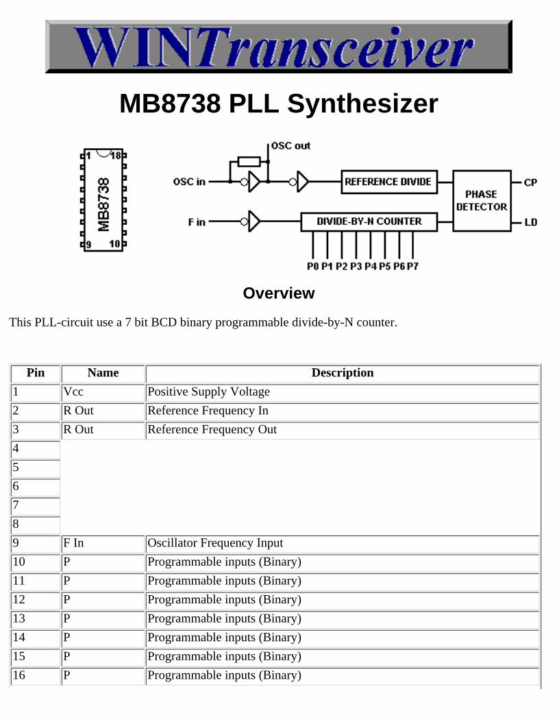
MB8738 PLL Synthesizer
Overview
This PLL-circuit use a 7 bit BCD binary programmable divide-by-N counter.
Pin Name Description
1 Vcc Positive Supply Voltage
2 R Out Reference Frequency In
3 R Out Reference Frequency Out
4
5
6
7
8
9 F In Oscillator Frequency Input
10 P Programmable inputs (Binary)
11 P Programmable inputs (Binary)
12 P Programmable inputs (Binary)
13 P Programmable inputs (Binary)
14 P Programmable inputs (Binary)
15 P Programmable inputs (Binary)
16 P Programmable inputs (Binary)

17 P Programmable inputs (Binary)
18 VSS GND Ground
CB Radio Banner Exchange
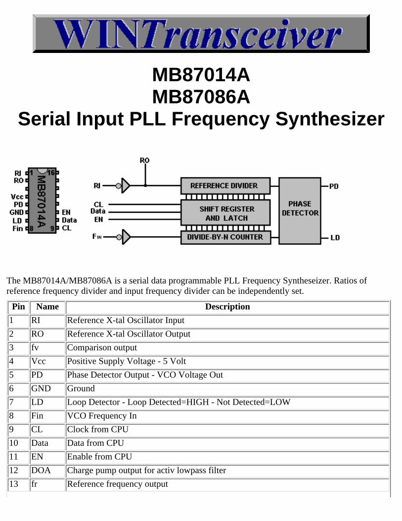
MB87014AMB87086A
Serial Input PLL Frequency Synthesizer
The MB87014A/MB87086A is a serial data programmable PLL Frequency Syntheseizer. Ratios ofreference frequency divider and input frequency divider can be independently set.
Pin Name Description
1 RI Reference X-tal Oscillator Input
2 RO Reference X-tal Oscillator Output
3 fv Comparison output
4 Vcc Positive Supply Voltage - 5 Volt
5 PD Phase Detector Output - VCO Voltage Out
6 GND Ground
7 LD Loop Detector - Loop Detected=HIGH - Not Detected=LOW
8 Fin VCO Frequency In
9 CL Clock from CPU
10 Data Data from CPU
11 EN Enable from CPU
12 DOA Charge pump output for activ lowpass filter
13 fr Reference frequency output
14 NC No Connection
15 OV Phase detector output to differential lowpass filter
16 OR Phase detector output to differential lowpass filter
CB Radio Banner Exchange
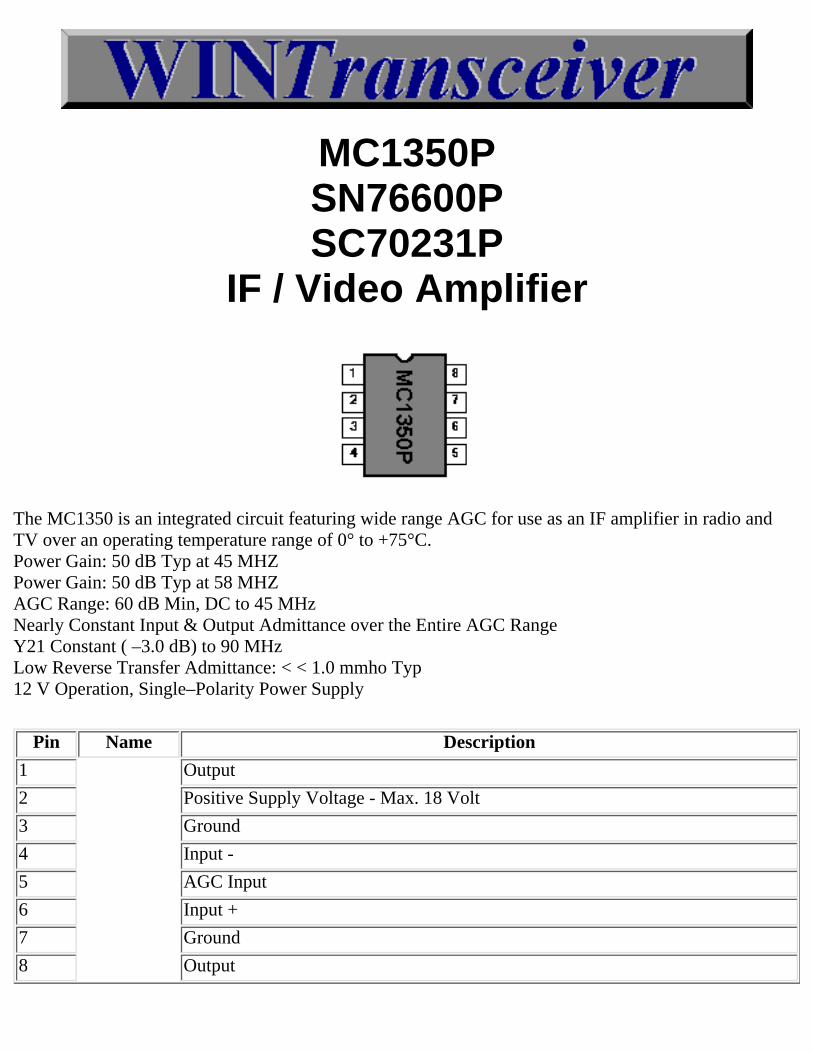
MC1350PSN76600PSC70231P
IF / Video Amplifier
The MC1350 is an integrated circuit featuring wide range AGC for use as an IF amplifier in radio andTV over an operating temperature range of 0° to +75°C.Power Gain: 50 dB Typ at 45 MHZPower Gain: 50 dB Typ at 58 MHZAGC Range: 60 dB Min, DC to 45 MHzNearly Constant Input & Output Admittance over the Entire AGC RangeY21 Constant ( –3.0 dB) to 90 MHzLow Reverse Transfer Admittance: < < 1.0 mmho Typ12 V Operation, Single–Polarity Power Supply
Pin Name Description
1 Output
2 Positive Supply Voltage - Max. 18 Volt
3 Ground
4 Input -
5 AGC Input
6 Input +
7 Ground
8 Output

CB Radio Banner Exchange
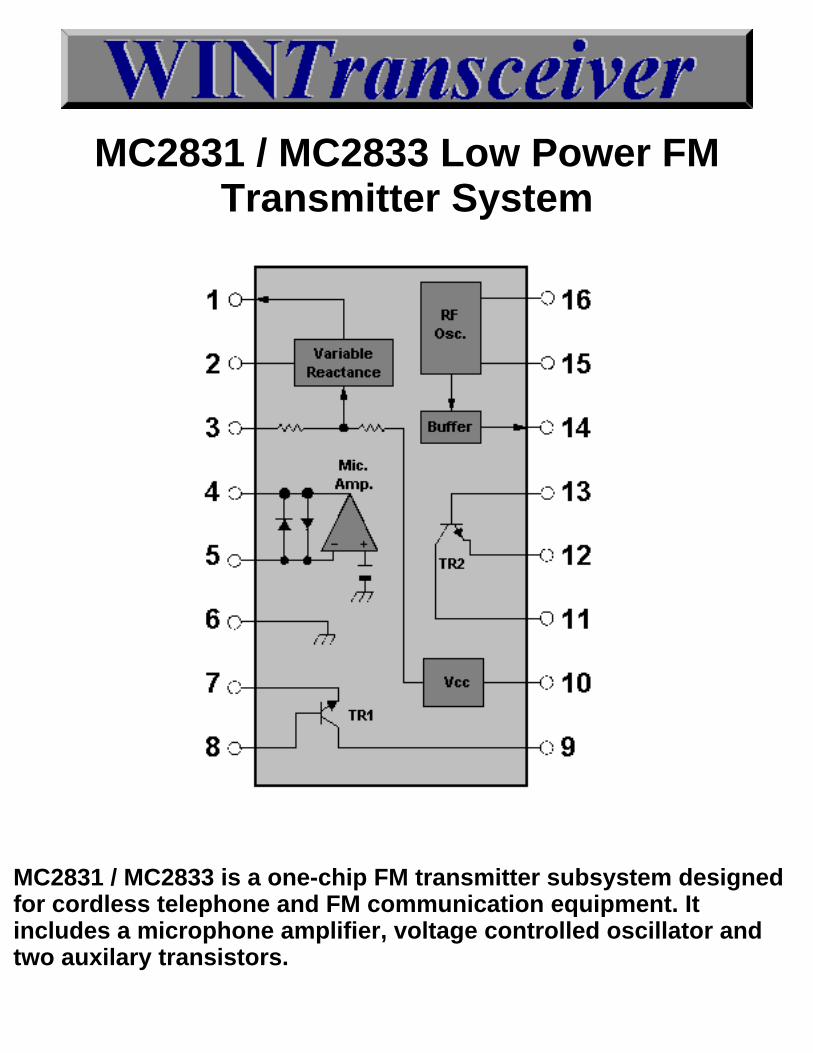
MC2831 / MC2833 Low Power FMTransmitter System
MC2831 / MC2833 is a one-chip FM transmitter subsystem designedfor cordless telephone and FM communication equipment. Itincludes a microphone amplifier, voltage controlled oscillator andtwo auxilary transistors.

CB Radio Banner Exchange
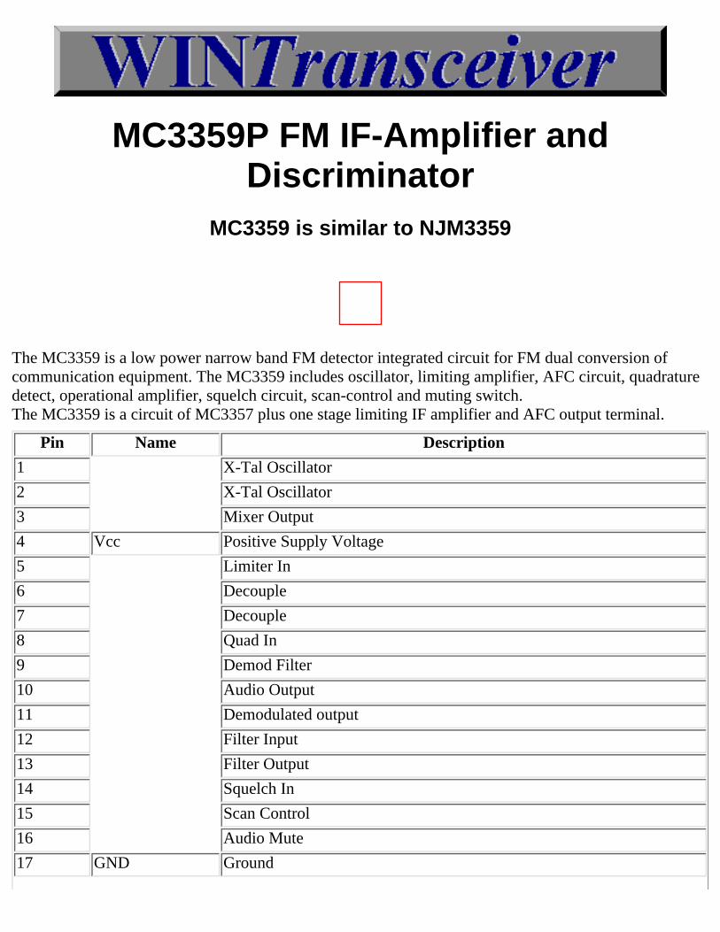
MC3359P FM IF-Amplifier andDiscriminator
MC3359 is similar to NJM3359
The MC3359 is a low power narrow band FM detector integrated circuit for FM dual conversion ofcommunication equipment. The MC3359 includes oscillator, limiting amplifier, AFC circuit, quadraturedetect, operational amplifier, squelch circuit, scan-control and muting switch.The MC3359 is a circuit of MC3357 plus one stage limiting IF amplifier and AFC output terminal.
Pin Name Description
1 X-Tal Oscillator
2 X-Tal Oscillator
3 Mixer Output
4 Vcc Positive Supply Voltage
5 Limiter In
6 Decouple
7 Decouple
8 Quad In
9 Demod Filter
10 Audio Output
11 Demodulated output
12 Filter Input
13 Filter Output
14 Squelch In
15 Scan Control
16 Audio Mute
17 GND Ground

18 RF Input
CB Radio Banner Exchange
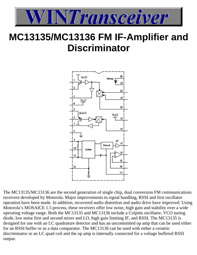
MC13135/MC13136 FM IF-Amplifier andDiscriminator
The MC13135/MC13136 are the second generation of single chip, dual conversion FM communicationsreceivers developed by Motorola. Major improvements in signal handling, RSSI and first oscillatoroperation have been made. In addition, recovered audio distortion and audio drive have improved. UsingMotorola’s MOSAICE 1.5 process, these receivers offer low noise, high gain and stability over a wideoperating voltage range. Both the MC13135 and MC13136 include a Colpitts oscillator, VCO tuningdiode, low noise first and second mixer and LO, high gain limiting IF, and RSSI. The MC13135 isdesigned for use with an LC quadrature detector and has an uncommitted op amp that can be used eitherfor an RSSI buffer or as a data comparator. The MC13136 can be used with either a ceramicdiscriminator or an LC quad coil and the op amp is internally connected for a voltage buffered RSSIoutput.

These devices can be used as stand–alone VHF receivers or as the lower IF of a triple conversion system.Applications include cordless telephones, short range data links, walkie–talkies, low cost land mobile,amateur radio receivers, baby monitors and scanners.Complete Dual Conversion FM Receiver – Antenna to Audio OutputInput Frequency Range – 200 MHzVoltage Buffered RSSI with 70 dB of Usable RangeLow Voltage Operation – 2.0 to 6.0 Vdc (2 Cell NiCad Supply)Low Current Drain – 3.5 mA TypLow Impedance Audio Output < 25 WVHF Colpitts First LO for Crystal or VCO OperationIsolated Tuning DiodeBuffered First LO Output to Drive CMOS PLL Synthesizer
CB Radio Banner Exchange
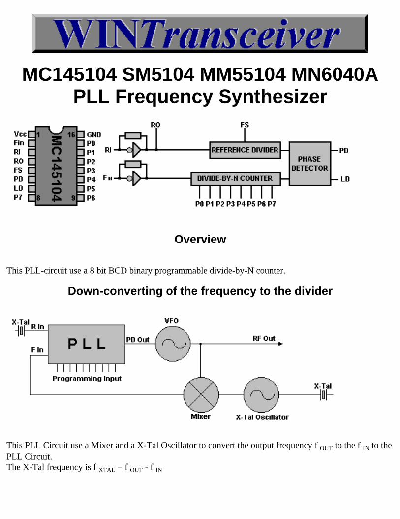
MC145104 SM5104 MM55104 MN6040APLL Frequency Synthesizer
Overview
This PLL-circuit use a 8 bit BCD binary programmable divide-by-N counter.
Down-converting of the frequency to the divider
This PLL Circuit use a Mixer and a X-Tal Oscillator to convert the output frequency f OUT to the f IN to thePLL Circuit.The X-Tal frequency is f XTAL = f OUT - f IN
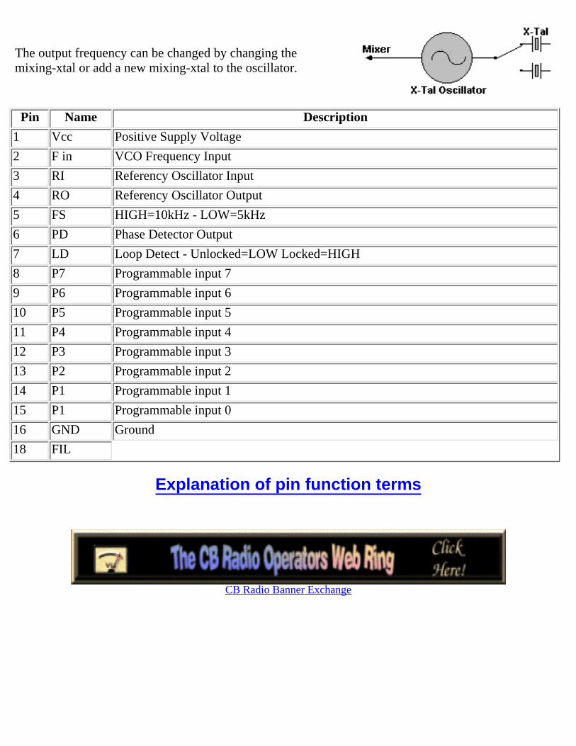
The output frequency can be changed by changing themixing-xtal or add a new mixing-xtal to the oscillator.
Pin Name Description
1 Vcc Positive Supply Voltage
2 F in VCO Frequency Input
3 RI Referency Oscillator Input
4 RO Referency Oscillator Output
5 FS HIGH=10kHz - LOW=5kHz
6 PD Phase Detector Output
7 LD Loop Detect - Unlocked=LOW Locked=HIGH
8 P7 Programmable input 7
9 P6 Programmable input 6
10 P5 Programmable input 5
11 P4 Programmable input 4
12 P3 Programmable input 3
13 P2 Programmable input 2
14 P1 Programmable input 1
15 P1 Programmable input 0
16 GND Ground
18 FIL
Explanation of pin function terms
CB Radio Banner Exchange
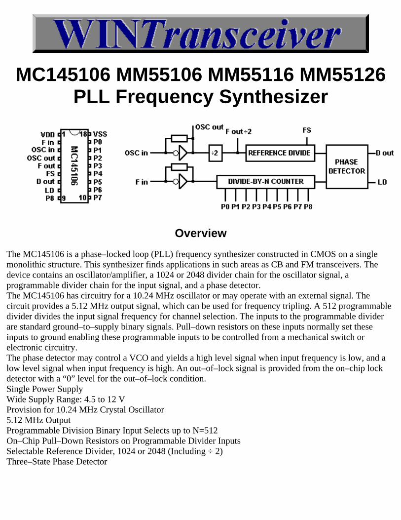
MC145106 MM55106 MM55116 MM55126PLL Frequency Synthesizer
Overview
The MC145106 is a phase–locked loop (PLL) frequency synthesizer constructed in CMOS on a singlemonolithic structure. This synthesizer finds applications in such areas as CB and FM transceivers. Thedevice contains an oscillator/amplifier, a 1024 or 2048 divider chain for the oscillator signal, aprogrammable divider chain for the input signal, and a phase detector.The MC145106 has circuitry for a 10.24 MHz oscillator or may operate with an external signal. Thecircuit provides a 5.12 MHz output signal, which can be used for frequency tripling. A 512 programmabledivider divides the input signal frequency for channel selection. The inputs to the programmable dividerare standard ground–to–supply binary signals. Pull–down resistors on these inputs normally set theseinputs to ground enabling these programmable inputs to be controlled from a mechanical switch orelectronic circuitry.The phase detector may control a VCO and yields a high level signal when input frequency is low, and alow level signal when input frequency is high. An out–of–lock signal is provided from the on–chip lockdetector with a “0” level for the out–of–lock condition.Single Power SupplyWide Supply Range: 4.5 to 12 VProvision for 10.24 MHz Crystal Oscillator5.12 MHz OutputProgrammable Division Binary Input Selects up to N=512On–Chip Pull–Down Resistors on Programmable Divider InputsSelectable Reference Divider, 1024 or 2048 (Including ÷ 2)Three–State Phase Detector
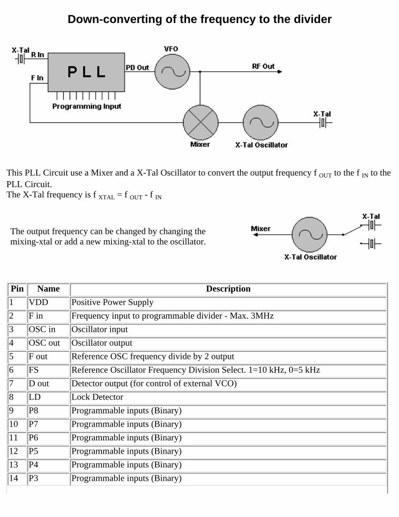
Down-converting of the frequency to the divider
This PLL Circuit use a Mixer and a X-Tal Oscillator to convert the output frequency f OUT to the f IN to thePLL Circuit.The X-Tal frequency is f XTAL = f OUT - f IN
The output frequency can be changed by changing themixing-xtal or add a new mixing-xtal to the oscillator.
Pin Name Description
1 VDD Positive Power Supply
2 F in Frequency input to programmable divider - Max. 3MHz
3 OSC in Oscillator input
4 OSC out Oscillator output
5 F out Reference OSC frequency divide by 2 output
6 FS Reference Oscillator Frequency Division Select. 1=10 kHz, 0=5 kHz
7 D out Detector output (for control of external VCO)
8 LD Lock Detector
9 P8 Programmable inputs (Binary)
10 P7 Programmable inputs (Binary)
11 P6 Programmable inputs (Binary)
12 P5 Programmable inputs (Binary)
13 P4 Programmable inputs (Binary)
14 P3 Programmable inputs (Binary)

15 P2 Programmable inputs (Binary)
16 P1 Programmable inputs (Binary)
17 P0 Programmable inputs (Binary)
18 VSS Ground
Explanation of pin function terms
TRUTH TABLE
P8 P7 P6 P5 P4 P3 P2 P1 P0 Divide by N
0 0 0 0 0 0 0 0 0 2
0 0 0 0 0 0 0 0 1 3
0 0 0 0 0 0 0 1 0 2
0 0 0 0 0 0 0 1 1 3
0 0 0 0 0 0 1 0 0 4
0 0 0 0 0 0 1 0 1 5
0 0 0 0 0 0 1 1 0 6
0 0 0 0 0 0 1 1 1 7
0 0 0 0 0 1 0 0 0 8
- - - - - - - - - -
- - - - - - - - - -
0 1 1 1 1 1 1 1 1 255
- - - - - - - - - -
- - - - - - - - - -
1 1 1 1 1 1 1 1 1 511
Uniden AM/FM/SSB Chassis
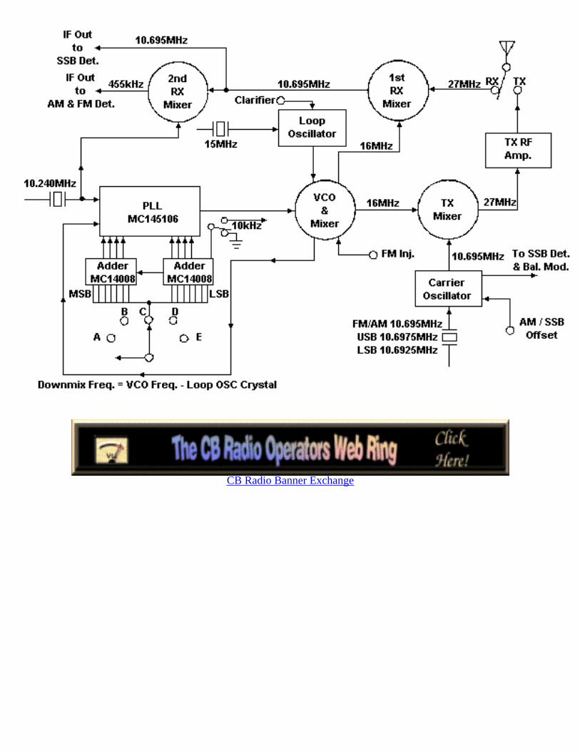
CB Radio Banner Exchange
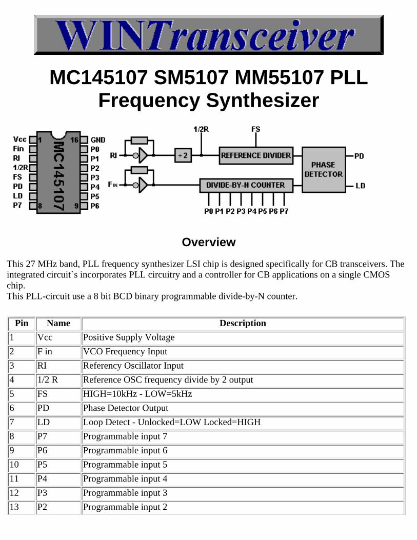
MC145107 SM5107 MM55107 PLLFrequency Synthesizer
Overview
This 27 MHz band, PLL frequency synthesizer LSI chip is designed specifically for CB transceivers. Theintegrated circuit`s incorporates PLL circuitry and a controller for CB applications on a single CMOSchip.This PLL-circuit use a 8 bit BCD binary programmable divide-by-N counter.
Pin Name Description
1 Vcc Positive Supply Voltage
2 F in VCO Frequency Input
3 RI Referency Oscillator Input
4 1/2 R Reference OSC frequency divide by 2 output
5 FS HIGH=10kHz - LOW=5kHz
6 PD Phase Detector Output
7 LD Loop Detect - Unlocked=LOW Locked=HIGH
8 P7 Programmable input 7
9 P6 Programmable input 6
10 P5 Programmable input 5
11 P4 Programmable input 4
12 P3 Programmable input 3
13 P2 Programmable input 2
14 P1 Programmable input 1
15 P1 Programmable input 0
16 GND Ground
Explanation of pin function terms
CB Radio Banner Exchange
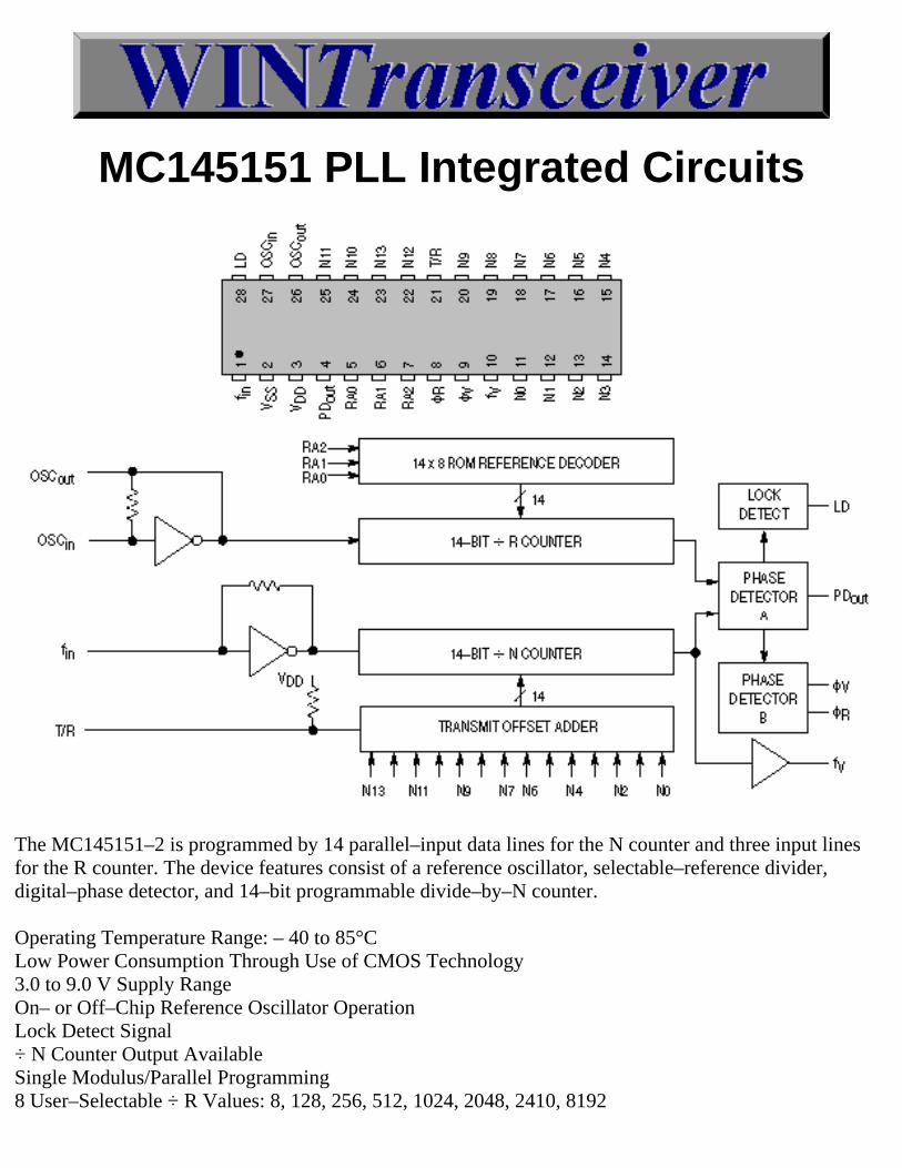
MC145151 PLL Integrated Circuits
The MC145151–2 is programmed by 14 parallel–input data lines for the N counter and three input linesfor the R counter. The device features consist of a reference oscillator, selectable–reference divider,digital–phase detector, and 14–bit programmable divide–by–N counter.
Operating Temperature Range: – 40 to 85°CLow Power Consumption Through Use of CMOS Technology3.0 to 9.0 V Supply RangeOn– or Off–Chip Reference Oscillator OperationLock Detect Signal÷ N Counter Output AvailableSingle Modulus/Parallel Programming8 User–Selectable ÷ R Values: 8, 128, 256, 512, 1024, 2048, 2410, 8192
÷ N Range = 3 to 16383“Linearized” Digital Phase Detector Enhances Transfer Function LinearityTwo Error Signal Options: Single–Ended (Three–State) or Double–EndedChip Complexity: 8000 FETs or 2000 Equivalent Gates
Pin Name Decription
1 FIN Frequency input - Max. 30MHz
2 GND Ground
3 VDD V+ (5 Volt)
4 PDOUT Phase Comparator Output
5 RA0 Reference divider Program input 0
6 RA1 Reference divider Program input 1
7 RA2 Reference divider Program input 2
8 øR Phase Comparator output
9 øV Phase Comparator output
10 f>SUB>V Program divider output
11 P0 Program input 0
12 P1 Program input 1
13 P2 Program input 2
14 P3 Program input 3
15 P4 Program input 4
16 P5 Program input 5
17 P6 Program input 6
18 P7 Program input 7
19 P8 Program input 8
20 P9 Program input 9
21 T/R Transmit / Receive
22 P12 Program input 12
23 P13 Program input 13
24 P10 Program input 10
25 P11 Program input 11
26 RO Referance Osc. Output
27 RI Referance Osc. Input
28 LD Loop Detect Output

Explanation of pin function terms
CB Radio Banner Exchange
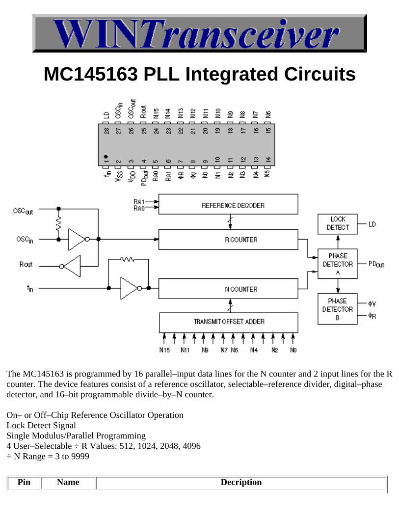
MC145163 PLL Integrated Circuits
The MC145163 is programmed by 16 parallel–input data lines for the N counter and 2 input lines for the Rcounter. The device features consist of a reference oscillator, selectable–reference divider, digital–phasedetector, and 16–bit programmable divide–by–N counter.
On– or Off–Chip Reference Oscillator OperationLock Detect SignalSingle Modulus/Parallel Programming4 User–Selectable ÷ R Values: 512, 1024, 2048, 4096÷ N Range = 3 to 9999
Pin Name Decription
1 FIN Frequency input - Max. 30MHz
2 GND Ground
3 VDD V+ (5 Volt)
4 PD Phase Comparator Output
5 RA0 Reference divider Program input 0
6 RA1 Reference divider Program input 1
7 øR Phase Comparator output
8 øV Phase Comparator output
9 P0 Program input 0
10 P1 Program input 1
11 P2 Program input 2
12 P3 Program input 3
13 P4 Program input 4
14 P5 Program input 5
15 P6 Program input 6
16 P7 Program input 7
17 P8 Program input 8
18 P9 Program input 9
19 P10 Program input 10
20 P11 Program input 11
21 P12 Program input 12
22 P13 Program input 13
23 P14 Program input 14
24 P15 Program input 15
25 ROUT Referance Osc. Output
26 RI Referance Osc. Input
27 RO Referance Osc. Output
28 L Loop Detect Output
Explanation of pin function terms
CB Radio Banner Exchange

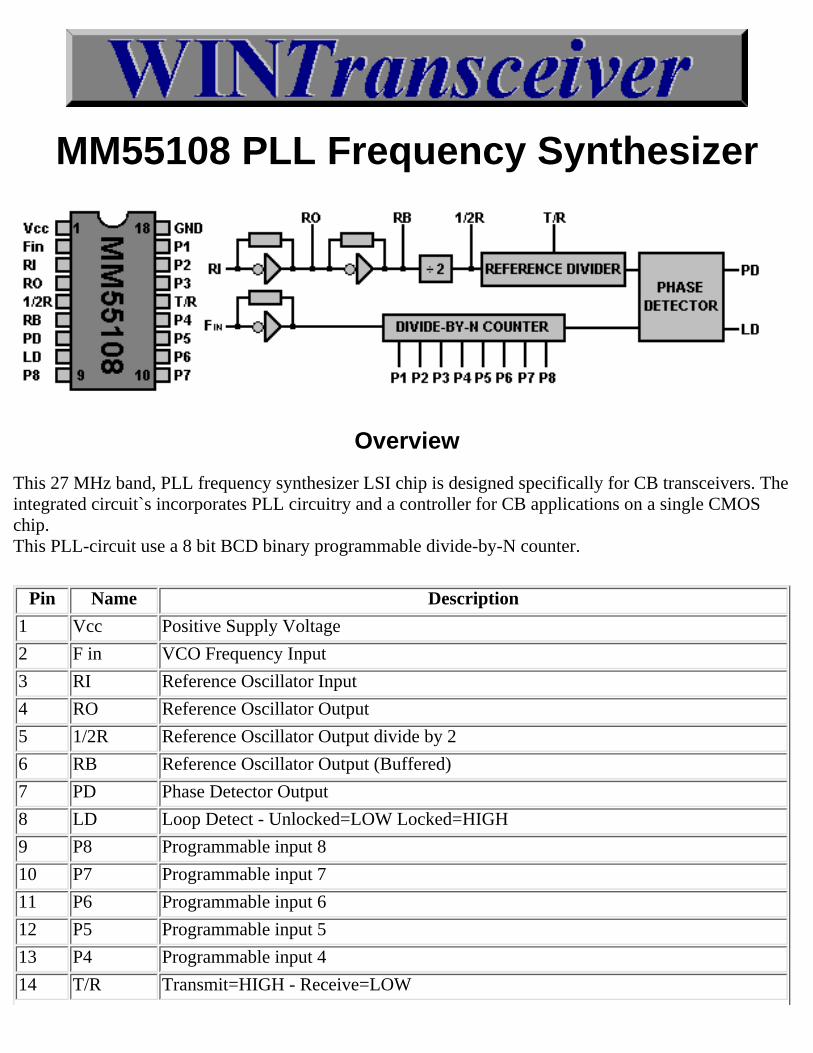
MM55108 PLL Frequency Synthesizer
Overview
This 27 MHz band, PLL frequency synthesizer LSI chip is designed specifically for CB transceivers. Theintegrated circuit`s incorporates PLL circuitry and a controller for CB applications on a single CMOSchip.This PLL-circuit use a 8 bit BCD binary programmable divide-by-N counter.
Pin Name Description
1 Vcc Positive Supply Voltage
2 F in VCO Frequency Input
3 RI Reference Oscillator Input
4 RO Reference Oscillator Output
5 1/2R Reference Oscillator Output divide by 2
6 RB Reference Oscillator Output (Buffered)
7 PD Phase Detector Output
8 LD Loop Detect - Unlocked=LOW Locked=HIGH
9 P8 Programmable input 8
10 P7 Programmable input 7
11 P6 Programmable input 6
12 P5 Programmable input 5
13 P4 Programmable input 4
14 T/R Transmit=HIGH - Receive=LOW
15 P3 Programmable input 3
16 P2 Programmable input 2
17 P1 Programmable input 1
18 GND Ground
CB Radio Banner Exchange

MSC42502P PLL Frequency Synthesizer
Overview
This PLL-circuit use a 8 bit BCD binary programmable divide-by-N counter.
Down-converting of the frequency to the divider
This PLL Circuit use a Mixer and a X-Tal Oscillator to convert the output frequency f OUT to the f IN to thePLL Circuit.The X-Tal frequency is f XTAL = f OUT - f IN
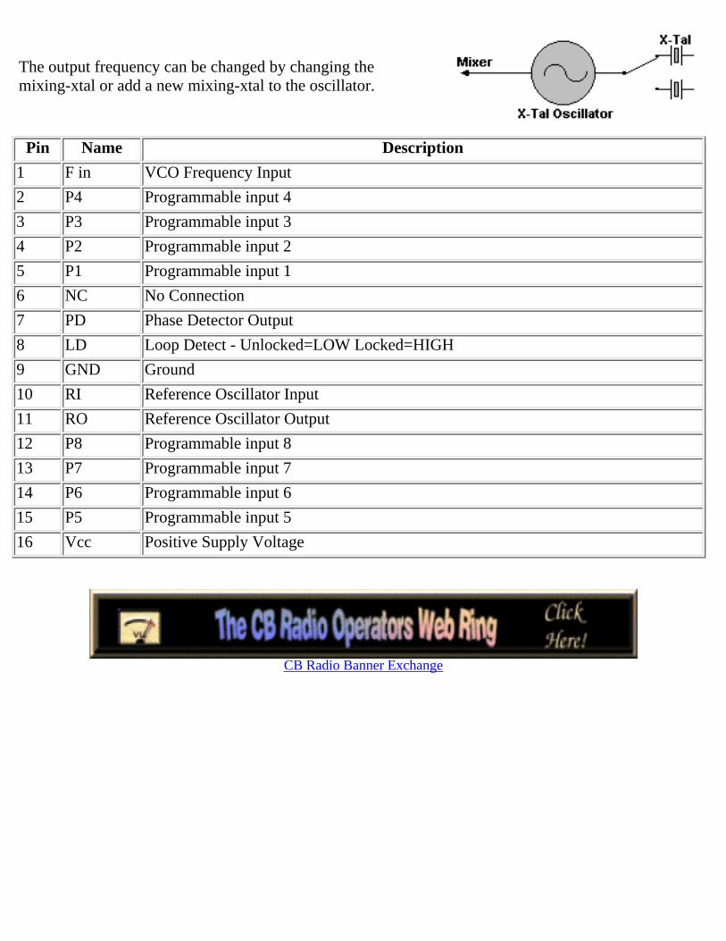
The output frequency can be changed by changing themixing-xtal or add a new mixing-xtal to the oscillator.
Pin Name Description
1 F in VCO Frequency Input
2 P4 Programmable input 4
3 P3 Programmable input 3
4 P2 Programmable input 2
5 P1 Programmable input 1
6 NC No Connection
7 PD Phase Detector Output
8 LD Loop Detect - Unlocked=LOW Locked=HIGH
9 GND Ground
10 RI Reference Oscillator Input
11 RO Reference Oscillator Output
12 P8 Programmable input 8
13 P7 Programmable input 7
14 P6 Programmable input 6
15 P5 Programmable input 5
16 Vcc Positive Supply Voltage
CB Radio Banner Exchange
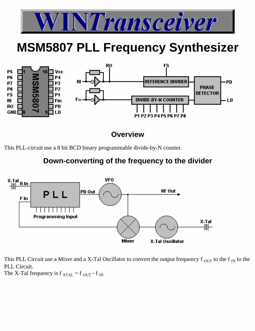
MSM5807 PLL Frequency Synthesizer
Overview
This PLL-circuit use a 8 bit BCD binary programmable divide-by-N counter.
Down-converting of the frequency to the divider
This PLL Circuit use a Mixer and a X-Tal Oscillator to convert the output frequency f OUT to the f IN to thePLL Circuit.The X-Tal frequency is f XTAL = f OUT - f IN
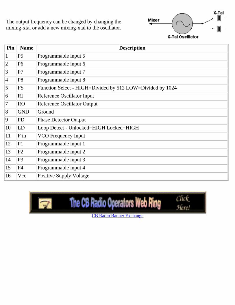
The output frequency can be changed by changing themixing-xtal or add a new mixing-xtal to the oscillator.
Pin Name Description
1 P5 Programmable input 5
2 P6 Programmable input 6
3 P7 Programmable input 7
4 P8 Programmable input 8
5 FS Function Select - HIGH=Divided by 512 LOW=Divided by 1024
6 RI Reference Oscillator Input
7 RO Reference Oscillator Output
8 GND Ground
9 PD Phase Detector Output
10 LD Loop Detect - Unlocked=HIGH Locked=HIGH
11 F in VCO Frequency Input
12 P1 Programmable input 1
13 P2 Programmable input 2
14 P3 Programmable input 3
15 P4 Programmable input 4
16 Vcc Positive Supply Voltage
CB Radio Banner Exchange

MSM5907 PLL Frequency Synthesizer
Pin Name Description
1 P4 Programmable input 4
2 P5 Programmable input 5
3 P6 Programmable input 6
4 P7 Programmable input 7
5 P8 Programmable input 8
6
7
8 GND Ground
9
10
11 F in VCO Frequency Input
12
13 P1 Programmable input 1
14 P2 Programmable input 2
15 P3 Programmable input 3
16 Vcc Positive Supply Voltage
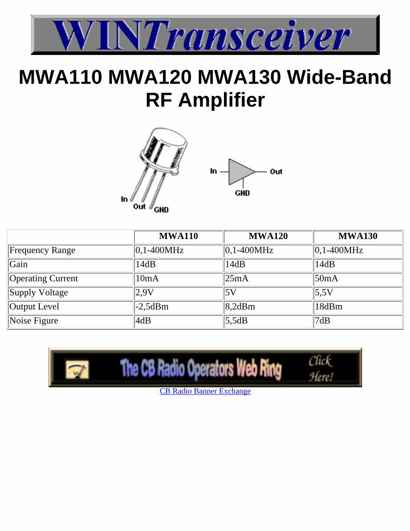
MWA110 MWA120 MWA130 Wide-BandRF Amplifier
MWA110 MWA120 MWA130
Frequency Range 0,1-400MHz 0,1-400MHz 0,1-400MHz
Gain 14dB 14dB 14dB
Operating Current 10mA 25mA 50mA
Supply Voltage 2,9V 5V 5,5V
Output Level -2,5dBm 8,2dBm 18dBm
Noise Figure 4dB 5,5dB 7dB
CB Radio Banner Exchange

NE602 NE612SA602A SA612A
Balanced RF Amplifier and Oscillator
The SA612A is a low-power VHF monolithic double-balanced mixer with on-board oscillator andvoltage regulator. It is intended for low cost, low power communication systems with signal frequenciesto 500MHz and local oscillator frequencies as high as 200MHz. The mixer is a “Gilbert cell” multiplierconfiguration which provides gain of 14dB or more at 45MHz. The oscillator can be configured for acrystal, a tuned tank operation, or as a buffer for an external L.O. Noise figure at 45MHz is typicallybelow 6dB and makes the device well suited for high performance cordless phone/cellular radio. The lowpower consumption makes the SA612A excellent for battery operated equipment. Networking and othercommunications products can benefit from very low radiated energy levels within systems. The SA612Ais available in an 8-lead dual in-line plastic package and an 8-lead SO (surface mounted miniaturepackage).
Pin Name Description
1 Input
2 Input
3 GND Ground
4 Output
5 Output
6 Oscillator Input
7 Oscillator Output
8 Vcc Supply Voltage

CB Radio Banner Exchange
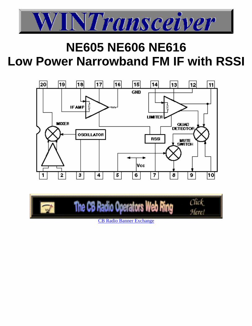
NE605 NE606 NE616Low Power Narrowband FM IF with RSSI
CB Radio Banner Exchange
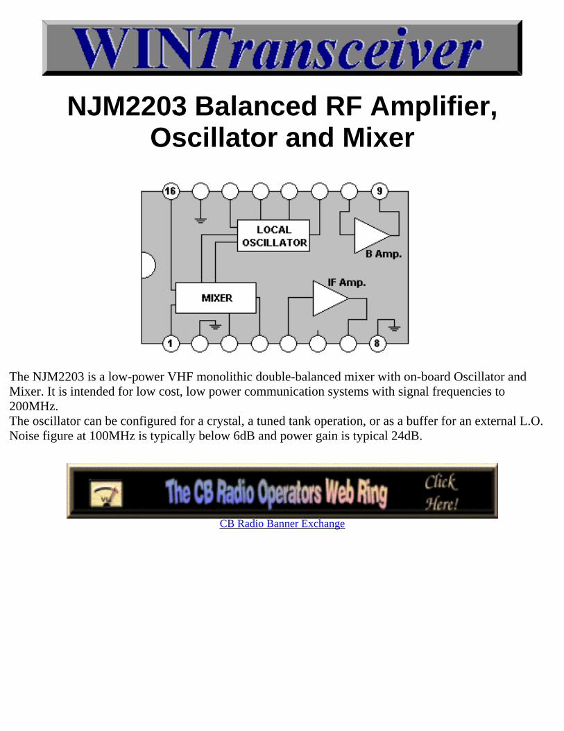
NJM2203 Balanced RF Amplifier,Oscillator and Mixer
The NJM2203 is a low-power VHF monolithic double-balanced mixer with on-board Oscillator andMixer. It is intended for low cost, low power communication systems with signal frequencies to200MHz.The oscillator can be configured for a crystal, a tuned tank operation, or as a buffer for an external L.O.Noise figure at 100MHz is typically below 6dB and power gain is typical 24dB.
CB Radio Banner Exchange
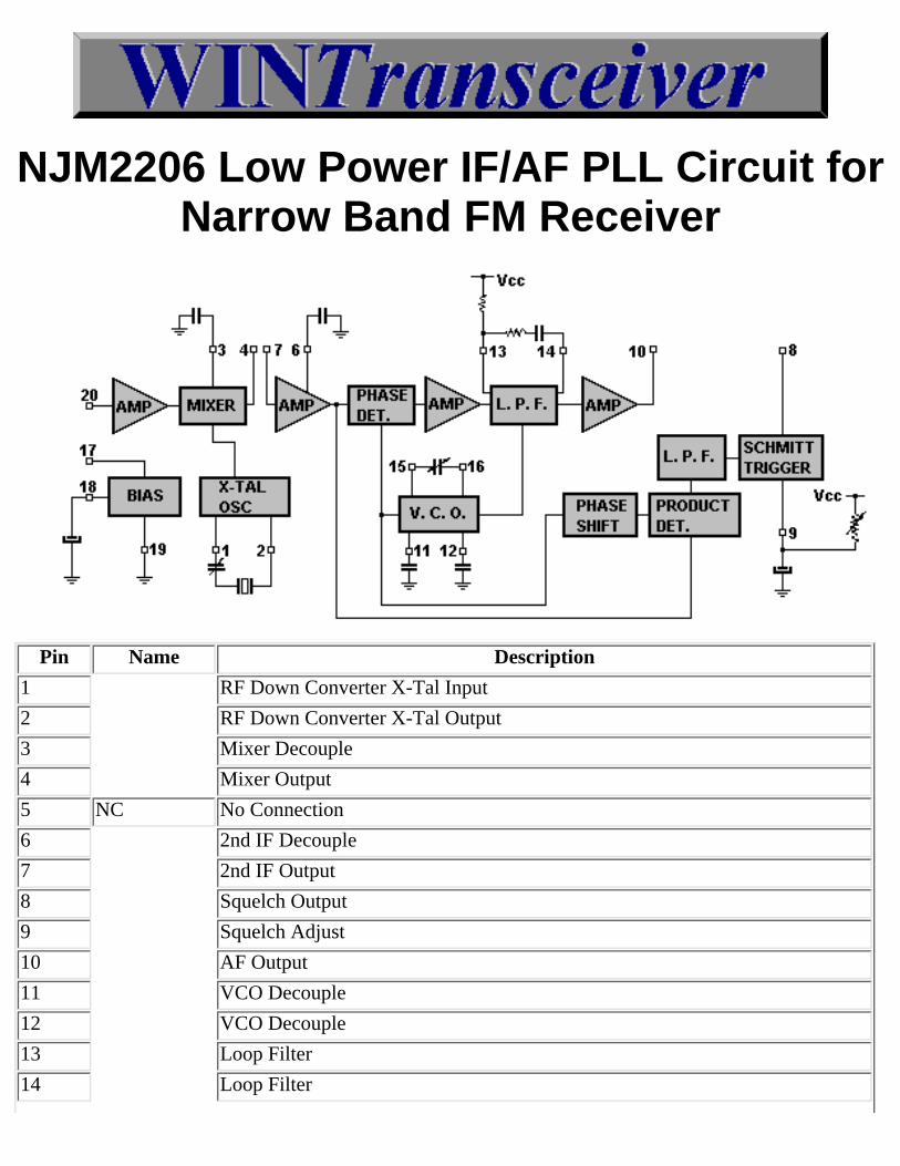
NJM2206 Low Power IF/AF PLL Circuit forNarrow Band FM Receiver
Pin Name Description
1 RF Down Converter X-Tal Input
2 RF Down Converter X-Tal Output
3 Mixer Decouple
4 Mixer Output
5 NC No Connection
6 2nd IF Decouple
7 2nd IF Output
8 Squelch Output
9 Squelch Adjust
10 AF Output
11 VCO Decouple
12 VCO Decouple
13 Loop Filter
14 Loop Filter
15 VCO Timing Capacitor
16 VCO Timing Capacitor
17 Vcc Positive Power Supply
18 Vcc Decouple
19 GND Ground
20 1st IF Input
CB Radio Banner Exchange
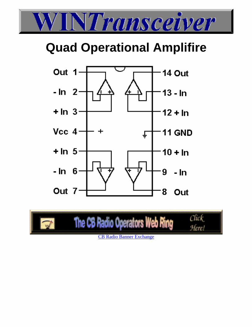
Quad Operational Amplifire
CB Radio Banner Exchange
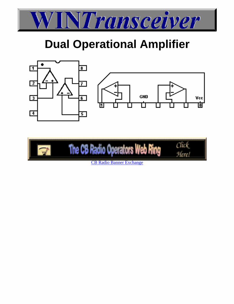
Dual Operational Amplifier
CB Radio Banner Exchange
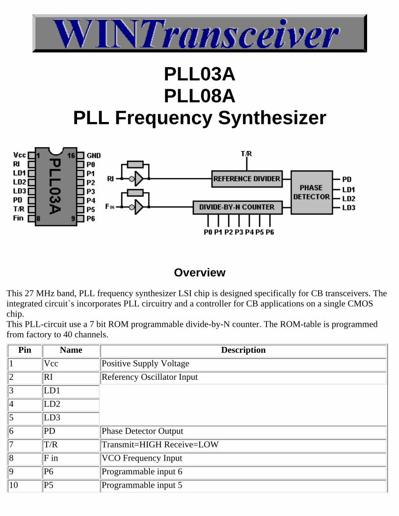
PLL03APLL08A
PLL Frequency Synthesizer
Overview
This 27 MHz band, PLL frequency synthesizer LSI chip is designed specifically for CB transceivers. Theintegrated circuit`s incorporates PLL circuitry and a controller for CB applications on a single CMOSchip.This PLL-circuit use a 7 bit ROM programmable divide-by-N counter. The ROM-table is programmedfrom factory to 40 channels.
Pin Name Description
1 Vcc Positive Supply Voltage
2 RI Referency Oscillator Input
3 LD1
4 LD2
5 LD3
6 PD Phase Detector Output
7 T/R Transmit=HIGH Receive=LOW
8 F in VCO Frequency Input
9 P6 Programmable input 6
10 P5 Programmable input 5
11 P4 Programmable input 4
12 P3 Programmable input 3
13 P2 Programmable input 2
14 P1 Programmable input 1
15 P1 Programmable input 0
26 GND Ground
Explanation of pin function terms
Programming Chart forPLL03A (U.S. - AM)PLL08A (EEC - FM)
Channel RXDivided by
TXDivided by
1 1206 1297
2 1208 1299
.. .... ....
22 1258 1349
.. .... ....
40 1294 1385
NOTES:1. Spesial divided by 2 circuit in TX mode change Referency Divider output to 2.5kHz steps.2. 91-count upshifts on TX provides 455kHz offset for receiver IF mixing when VCO frequency isdoubled.3. Sinse chip cannot divide VCO directly, they are down-mixed with the 10.240MHz Referency Oscillatorsignal, produsing 6MHz outputs (RX Mode) and 3MHz outputs (TX Mode) into dividers. Standard16MHz VCO is used.4. PLL08A contains only the first 22 FCC channels for EEC use; otherwise both chip are identical.
Example of VCO Determination, Channel 1:1206 x 5kHz + 10.240MHz = 16.270MHz (RX-Mode)1297 x 2.5kHz + 10.240MHz = 13.4825MHz (TX-Mode)(13.4825MHz x 2 = 26.965MHz)

CB Radio Banner Exchange
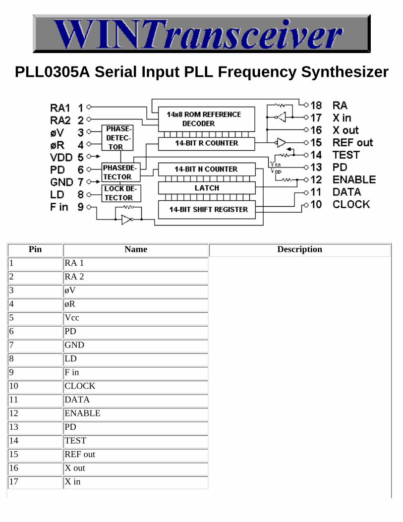
PLL0305A Serial Input PLL Frequency Synthesizer
Pin Name Description
1 RA 1
2 RA 2
3 øV
4 øR
5 Vcc
6 PD
7 GND
8 LD
9 F in
10 CLOCK
11 DATA
12 ENABLE
13 PD
14 TEST
15 REF out
16 X out
17 X in

18 RA 0
CB Radio Banner Exchange

PLL2002A Serial Input PLL FrequencySynthesizer
The PLL2002A is a serial data programmable PLL Frequency Syntheseizer. Ratios of referencefrequency divider and input frequency divider can be independently set.
Pin Name Description
1 RI Reference X-tal Oscillator Input
2 RO Reference X-tal Oscillator Output
3 NC No Connection
4 Vcc Positive Supply Voltage - 5 Volt
5 PD Phase Detector Output - VCO Voltage Out
6 GND Ground
7 LD Loop Detector - Loop Detected=HIGH - Not Detected=LOW
8 Fin VCO Frequency In
9 CL Clock from CPU
10 Data Data from CPU
11 EN Enable from CPU
12 DOA Charge pump output for activ lowpass filter
13 NC No Connection
14 Test Connect to Vcc
15 OV Phase detector output to differential lowpass filter
16 OR Phase detector output to differential lowpass filter
Serial Data for PLL2002A
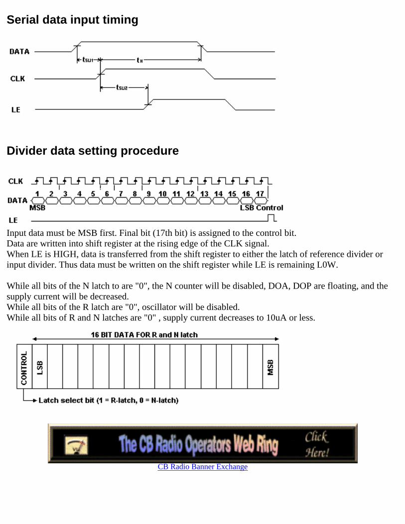
Serial data input timing
Divider data setting procedure
Input data must be MSB first. Final bit (17th bit) is assigned to the control bit.Data are written into shift register at the rising edge of the CLK signal.When LE is HIGH, data is transferred from the shift register to either the latch of reference divider orinput divider. Thus data must be written on the shift register while LE is remaining L0W.
While all bits of the N latch to are "0", the N counter will be disabled, DOA, DOP are floating, and thesupply current will be decreased.While all bits of the R latch are "0", oscillator will be disabled.While all bits of R and N latches are "0" , supply current decreases to 10uA or less.
CB Radio Banner Exchange
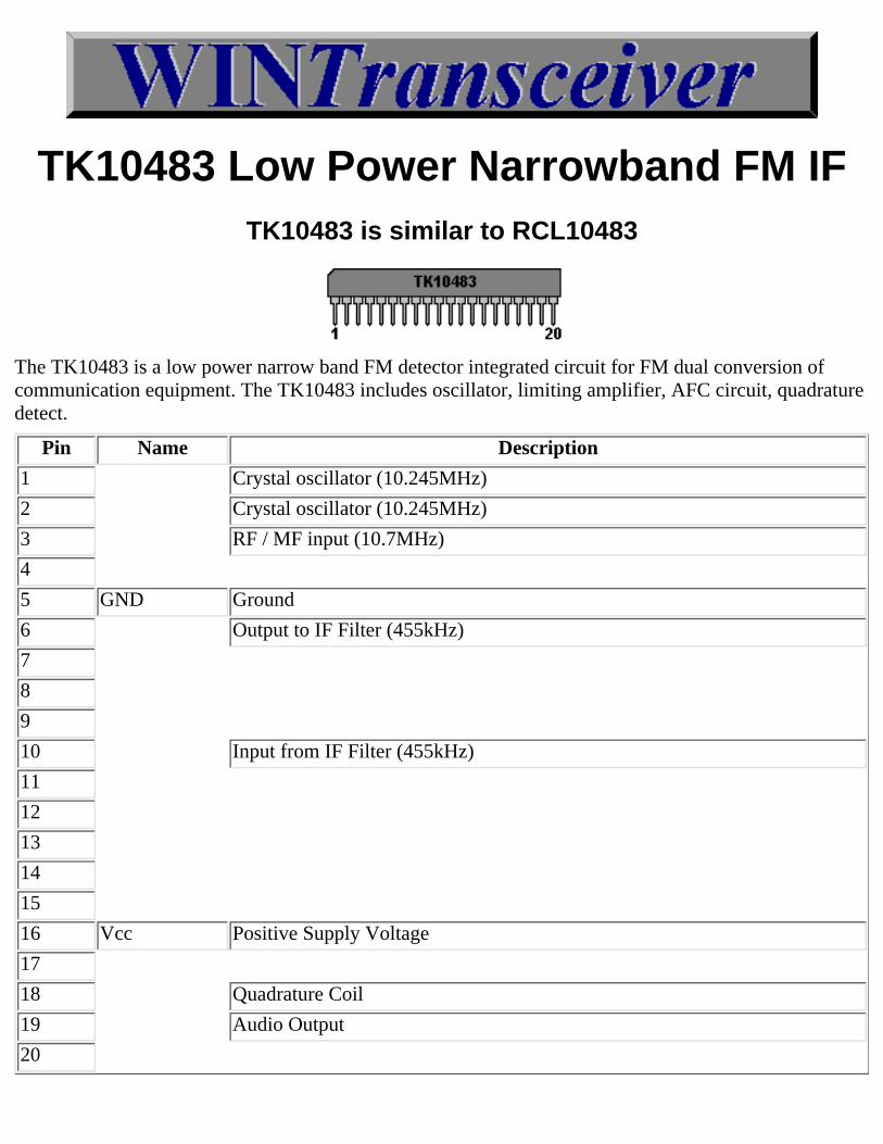
TK10483 Low Power Narrowband FM IFTK10483 is similar to RCL10483
The TK10483 is a low power narrow band FM detector integrated circuit for FM dual conversion ofcommunication equipment. The TK10483 includes oscillator, limiting amplifier, AFC circuit, quadraturedetect.
Pin Name Description
1 Crystal oscillator (10.245MHz)
2 Crystal oscillator (10.245MHz)
3 RF / MF input (10.7MHz)
4
5 GND Ground
6 Output to IF Filter (455kHz)
7
8
9
10 Input from IF Filter (455kHz)
11
12
13
14
15
16 Vcc Positive Supply Voltage
17
18 Quadrature Coil
19 Audio Output
20

CB Radio Banner Exchange
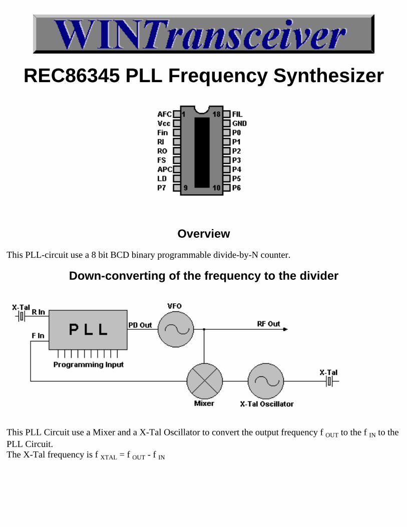
REC86345 PLL Frequency Synthesizer
Overview
This PLL-circuit use a 8 bit BCD binary programmable divide-by-N counter.
Down-converting of the frequency to the divider
This PLL Circuit use a Mixer and a X-Tal Oscillator to convert the output frequency f OUT to the f IN to thePLL Circuit.The X-Tal frequency is f XTAL = f OUT - f IN
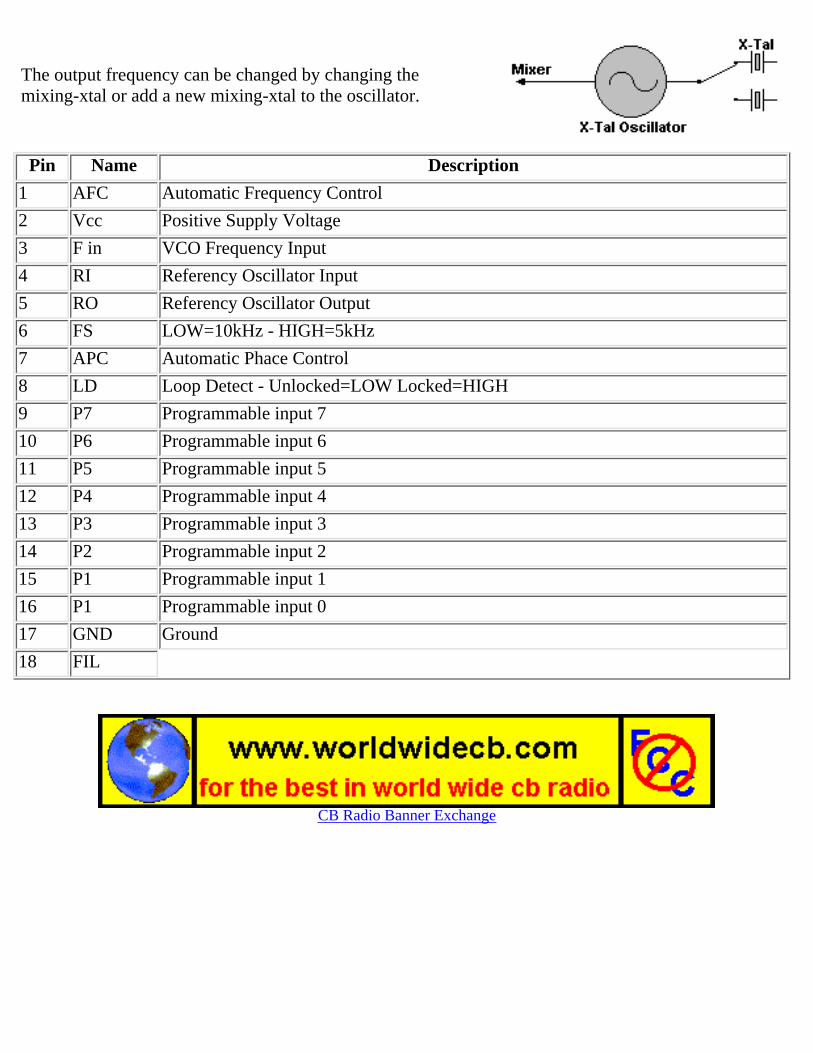
The output frequency can be changed by changing themixing-xtal or add a new mixing-xtal to the oscillator.
Pin Name Description
1 AFC Automatic Frequency Control
2 Vcc Positive Supply Voltage
3 F in VCO Frequency Input
4 RI Referency Oscillator Input
5 RO Referency Oscillator Output
6 FS LOW=10kHz - HIGH=5kHz
7 APC Automatic Phace Control
8 LD Loop Detect - Unlocked=LOW Locked=HIGH
9 P7 Programmable input 7
10 P6 Programmable input 6
11 P5 Programmable input 5
12 P4 Programmable input 4
13 P3 Programmable input 3
14 P2 Programmable input 2
15 P1 Programmable input 1
16 P1 Programmable input 0
17 GND Ground
18 FIL
CB Radio Banner Exchange
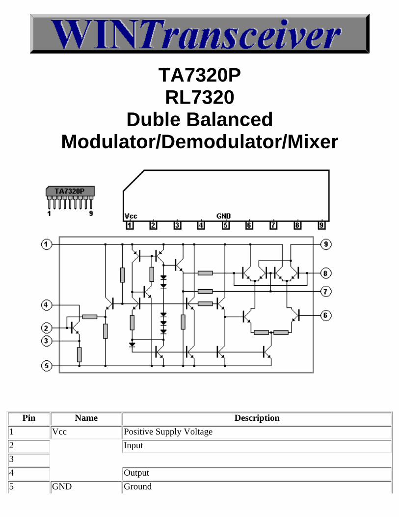
TA7320PRL7320
Duble BalancedModulator/Demodulator/Mixer
Pin Name Description
1 Vcc Positive Supply Voltage
2 Input
3
4 Output
5 GND Ground
6 Input
7
8 Input
9 Output
CB Radio Banner Exchange
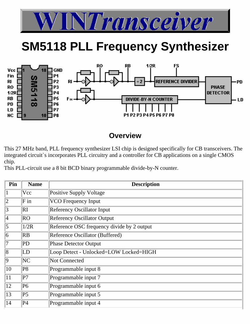
SM5118 PLL Frequency Synthesizer
Overview
This 27 MHz band, PLL frequency synthesizer LSI chip is designed specifically for CB transceivers. Theintegrated circuit`s incorporates PLL circuitry and a controller for CB applications on a single CMOSchip.This PLL-circuit use a 8 bit BCD binary programmable divide-by-N counter.
Pin Name Description
1 Vcc Positive Supply Voltage
2 F in VCO Frequency Input
3 RI Referency Oscillator Input
4 RO Referency Oscillator Output
5 1/2R Reference OSC frequency divide by 2 output
6 RB Reference Oscillator (Buffered)
7 PD Phase Detector Output
8 LD Loop Detect - Unlocked=LOW Locked=HIGH
9 NC Not Connected
10 P8 Programmable input 8
11 P7 Programmable input 7
12 P6 Programmable input 6
13 P5 Programmable input 5
14 P4 Programmable input 4

15 P3 Programmable input 3
16 P2 Programmable input 2
17 P1 Programmable input 1
18 GND Ground
Explanation of pin function terms
CB Radio Banner Exchange
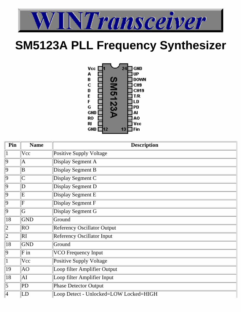
SM5123A PLL Frequency Synthesizer
Pin Name Description
1 Vcc Positive Supply Voltage
9 A Display Segment A
9 B Display Segment B
9 C Display Segment C
9 D Display Segment D
9 E Display Segment E
9 F Display Segment F
9 G Display Segment G
18 GND Ground
2 RO Referency Oscillator Output
2 RI Referency Oscillator Input
18 GND Ground
9 F in VCO Frequency Input
1 Vcc Positive Supply Voltage
19 AO Loop filter Amplifier Output
18 AI Loop filter Amplifier Input
5 PD Phase Detector Output
4 LD Loop Detect - Unlocked=LOW Locked=HIGH

9 T/R Transmit=LOW Receive=HIGH
18 CH19 Channel 19
18 CH19 Channel 19
18 DOWN Channel DOWN
18 UP Channel UP
18 GND Ground
Explanation of pin function terms
CB Radio Banner Exchange
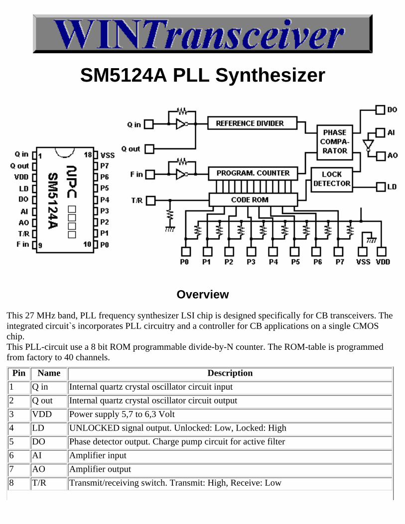
SM5124A PLL Synthesizer
Overview
This 27 MHz band, PLL frequency synthesizer LSI chip is designed specifically for CB transceivers. Theintegrated circuit`s incorporates PLL circuitry and a controller for CB applications on a single CMOSchip.This PLL-circuit use a 8 bit ROM programmable divide-by-N counter. The ROM-table is programmedfrom factory to 40 channels.
Pin Name Description
1 Q in Internal quartz crystal oscillator circuit input
2 Q out Internal quartz crystal oscillator circuit output
3 VDD Power supply 5,7 to 6,3 Volt
4 LD UNLOCKED signal output. Unlocked: Low, Locked: High
5 DO Phase detector output. Charge pump circuit for active filter
6 AI Amplifier input
7 AO Amplifier output
8 T/R Transmit/receiving switch. Transmit: High, Receive: Low
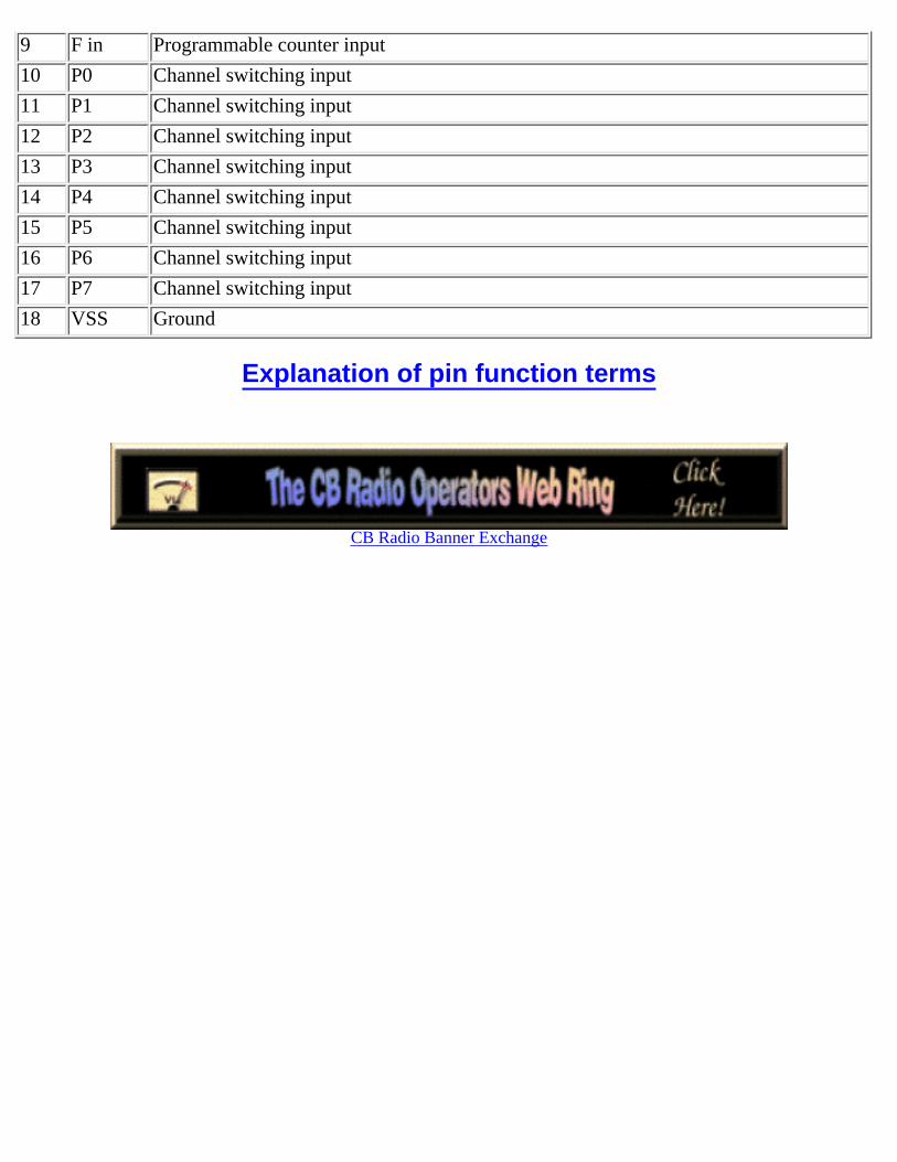
9 F in Programmable counter input
10 P0 Channel switching input
11 P1 Channel switching input
12 P2 Channel switching input
13 P3 Channel switching input
14 P4 Channel switching input
15 P5 Channel switching input
16 P6 Channel switching input
17 P7 Channel switching input
18 VSS Ground
Explanation of pin function terms
CB Radio Banner Exchange
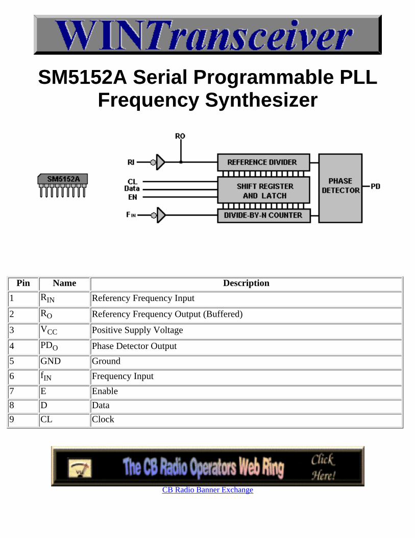
SM5152A Serial Programmable PLLFrequency Synthesizer
Pin Name Description
1 RIN Referency Frequency Input
2 RO Referency Frequency Output (Buffered)
3 VCC Positive Supply Voltage
4 PDO Phase Detector Output
5 GND Ground
6 fIN Frequency Input
7 E Enable
8 D Data
9 CL Clock
CB Radio Banner Exchange

SM5158A Serial Input PLL FrequencySynthesizer
Pin Name Description
1
2
3
4
5
6
7
8
9
10
11
12
13
14
15
16
Explanation of pin function terms
CB Radio Banner Exchange
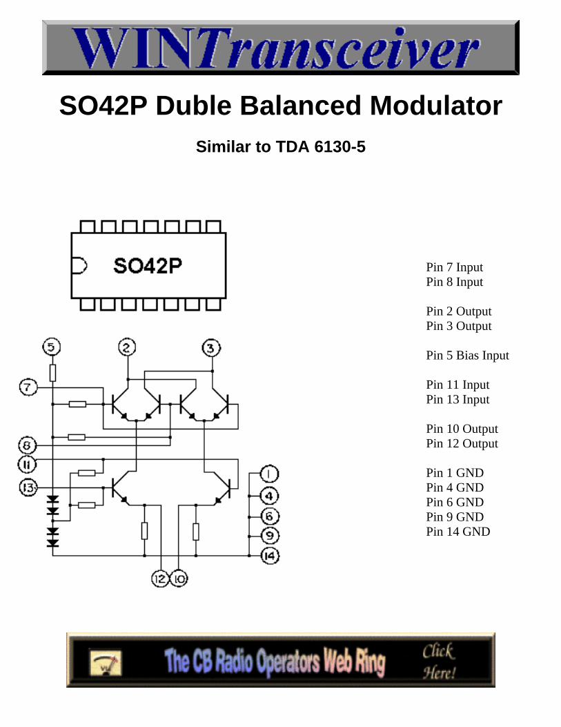
SO42P Duble Balanced ModulatorSimilar to TDA 6130-5
Pin 7 InputPin 8 Input
Pin 2 OutputPin 3 Output
Pin 5 Bias Input
Pin 11 InputPin 13 Input
Pin 10 OutputPin 12 Output
Pin 1 GNDPin 4 GNDPin 6 GNDPin 9 GNDPin 14 GND
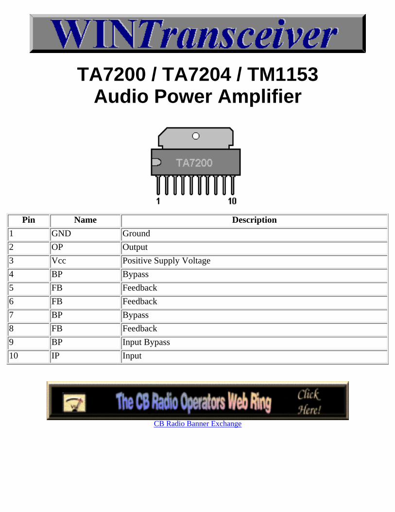
TA7200 / TA7204 / TM1153Audio Power Amplifier
Pin Name Description
1 GND Ground
2 OP Output
3 Vcc Positive Supply Voltage
4 BP Bypass
5 FB Feedback
6 FB Feedback
7 BP Bypass
8 FB Feedback
9 BP Input Bypass
10 IP Input
CB Radio Banner Exchange
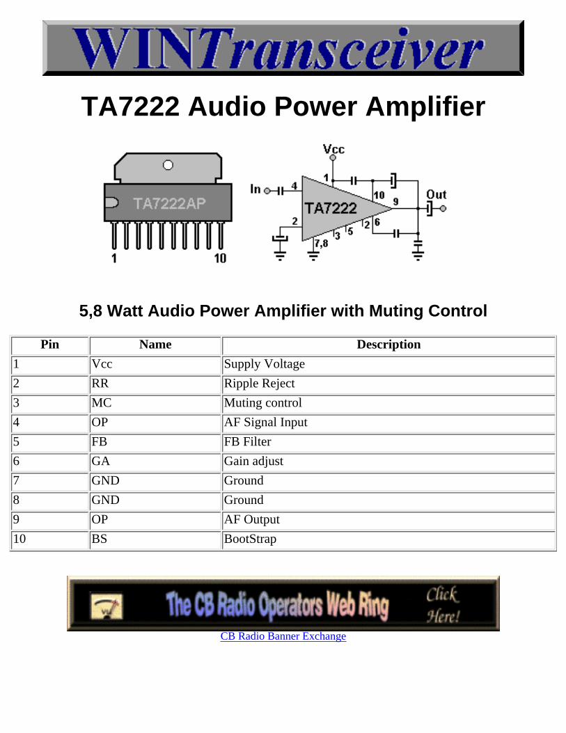
TA7222 Audio Power Amplifier
5,8 Watt Audio Power Amplifier with Muting Control
Pin Name Description
1 Vcc Supply Voltage
2 RR Ripple Reject
3 MC Muting control
4 OP AF Signal Input
5 FB FB Filter
6 GA Gain adjust
7 GND Ground
8 GND Ground
9 OP AF Output
10 BS BootStrap
CB Radio Banner Exchange
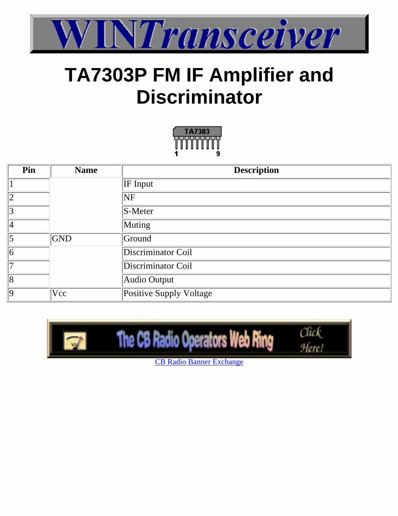
TA7303P FM IF Amplifier andDiscriminator
Pin Name Description
1 IF Input
2 NF
3 S-Meter
4 Muting
5 GND Ground
6 Discriminator Coil
7 Discriminator Coil
8 Audio Output
9 Vcc Positive Supply Voltage
CB Radio Banner Exchange
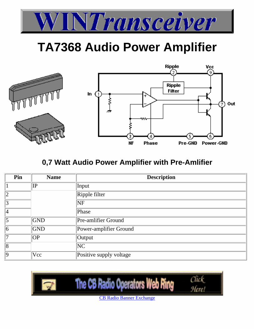
TA7368 Audio Power Amplifier
0,7 Watt Audio Power Amplifier with Pre-Amlifier
Pin Name Description
1 IP Input
2 Ripple filter
3 NF
4 Phase
5 GND Pre-amlifier Ground
6 GND Power-amplifier Ground
7 OP Output
8 NC
9 Vcc Positive supply voltage
CB Radio Banner Exchange
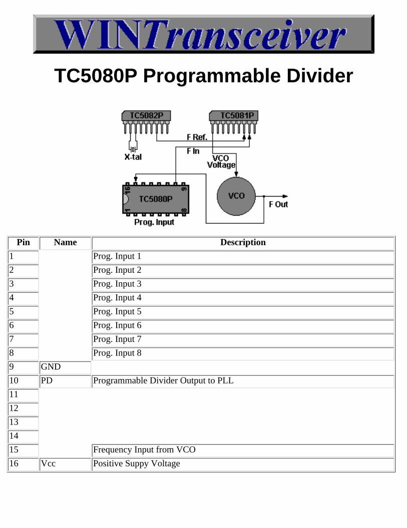
TC5080P Programmable Divider
Pin Name Description
1 Prog. Input 1
2 Prog. Input 2
3 Prog. Input 3
4 Prog. Input 4
5 Prog. Input 5
6 Prog. Input 6
7 Prog. Input 7
8 Prog. Input 8
9 GND
10 PD Programmable Divider Output to PLL
11
12
13
14
15 Frequency Input from VCO
16 Vcc Positive Suppy Voltage
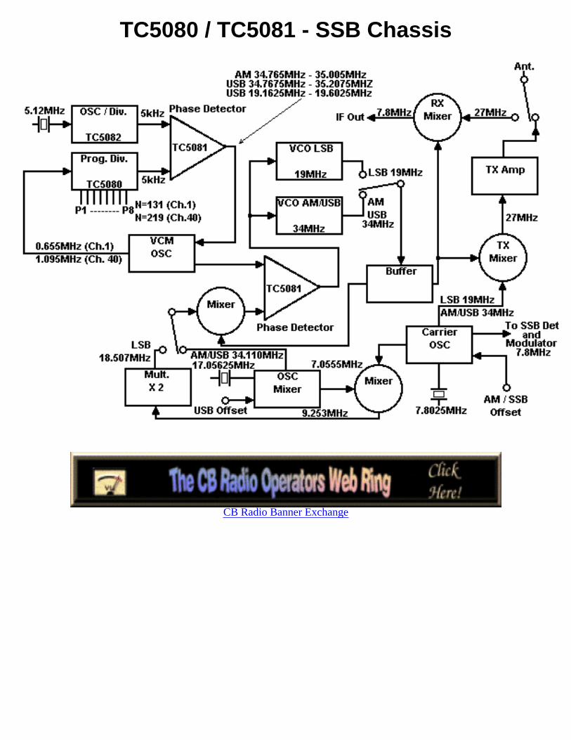
TC5080 / TC5081 - SSB Chassis
CB Radio Banner Exchange
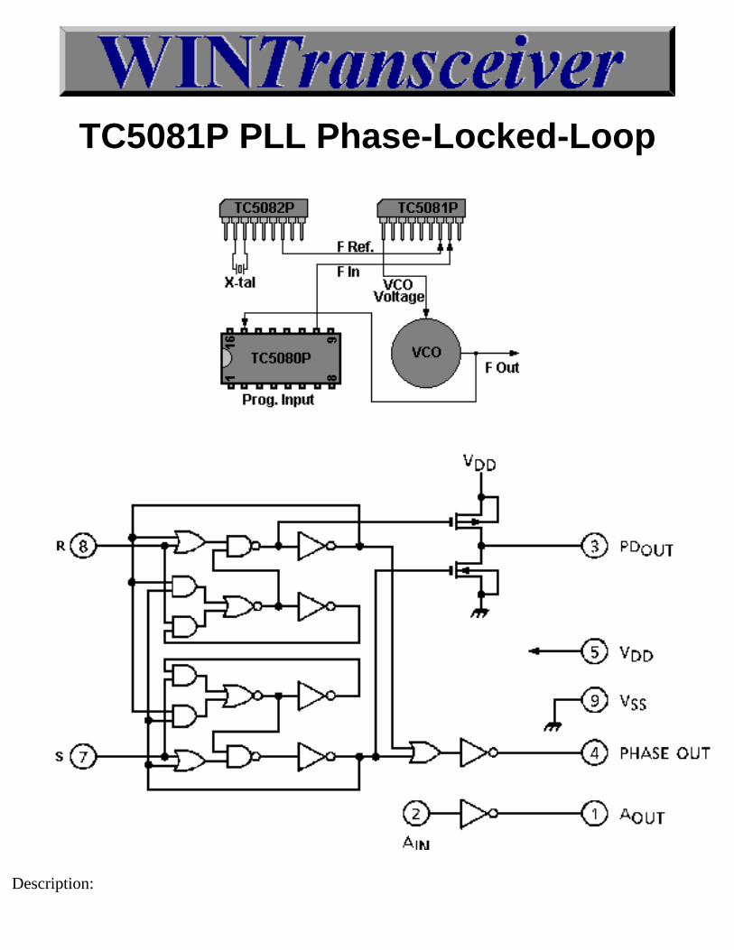
TC5081P PLL Phase-Locked-Loop
Description:
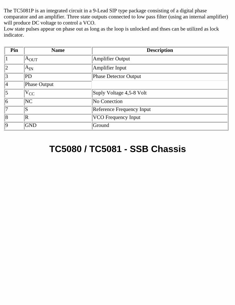
The TC5081P is an integrated circuit in a 9-Lead SIP type package consisting of a digital phasecomparator and an amplifier. Three state outputs connected to low pass filter (using an internal amplifier)will produce DC voltage to control a VCO.Low state pulses appear on phase out as long as the loop is unlocked and thses can be utilized as lockindicator.
Pin Name Description
1 AOUT Amplifier Output
2 AIN Amplifier Input
3 PD Phase Detector Output
4 Phase Output
5 VCC Suply Voltage 4,5-8 Volt
6 NC No Conection
7 S Reference Frequency Input
8 R VCO Frequency Input
9 GND Ground
TC5080 / TC5081 - SSB Chassis
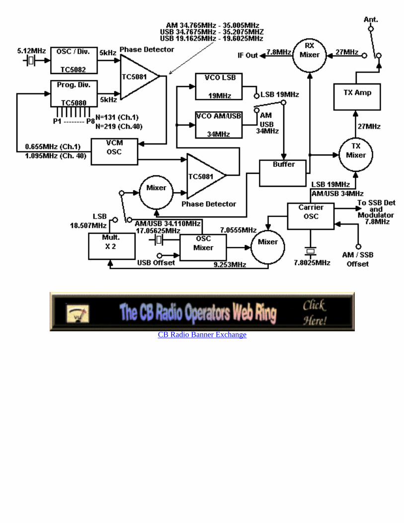
CB Radio Banner Exchange
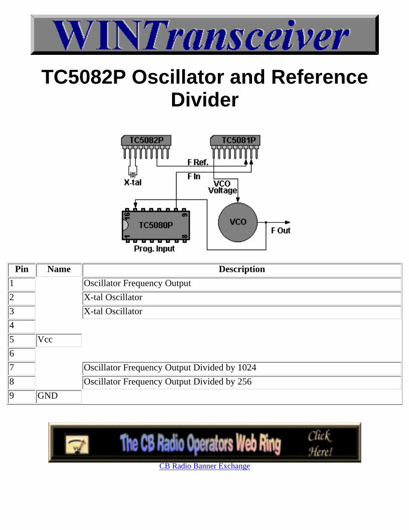
TC5082P Oscillator and ReferenceDivider
Pin Name Description
1 Oscillator Frequency Output
2 X-tal Oscillator
3 X-tal Oscillator
4
5 Vcc
6
7 Oscillator Frequency Output Divided by 1024
8 Oscillator Frequency Output Divided by 256
9 GND
CB Radio Banner Exchange
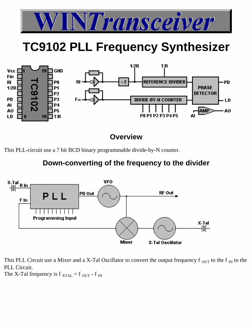
TC9102 PLL Frequency Synthesizer
Overview
This PLL-circuit use a 7 bit BCD binary programmable divide-by-N counter.
Down-converting of the frequency to the divider
This PLL Circuit use a Mixer and a X-Tal Oscillator to convert the output frequency f OUT to the f IN to thePLL Circuit.The X-Tal frequency is f XTAL = f OUT - f IN
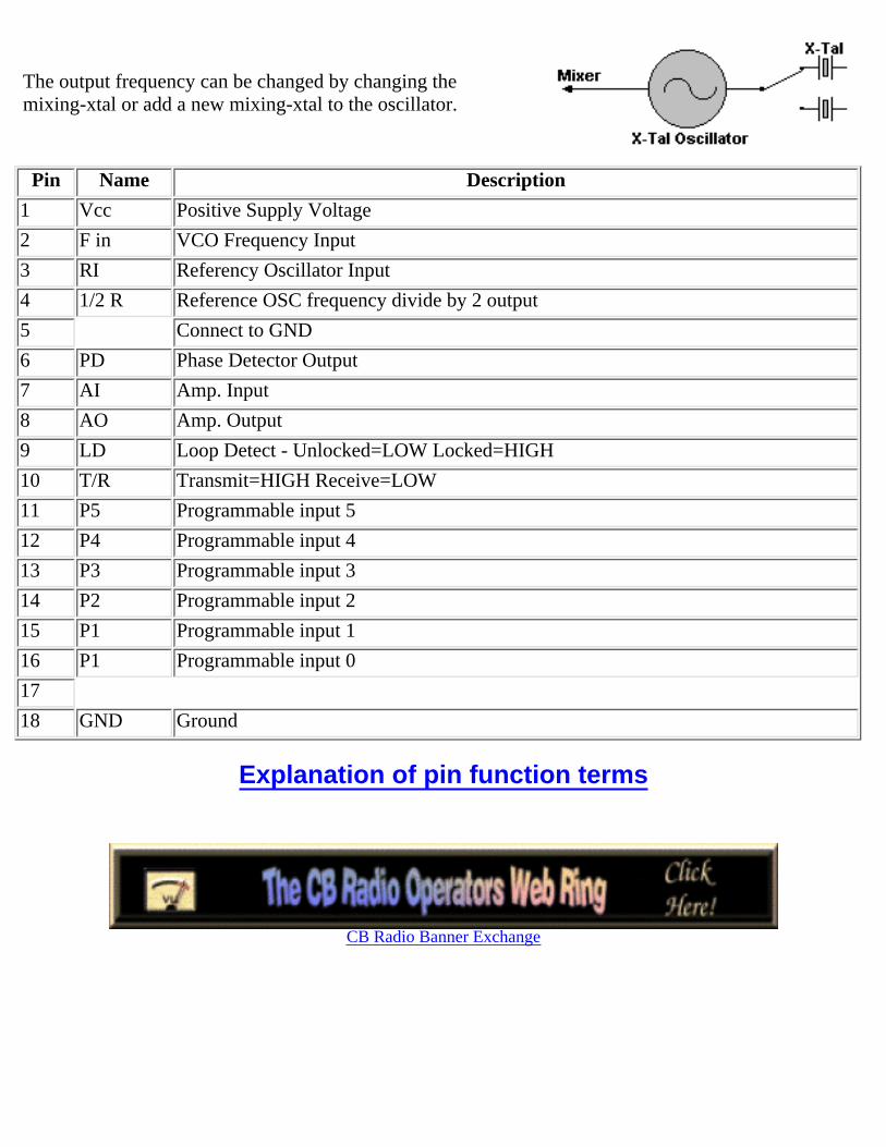
The output frequency can be changed by changing themixing-xtal or add a new mixing-xtal to the oscillator.
Pin Name Description
1 Vcc Positive Supply Voltage
2 F in VCO Frequency Input
3 RI Referency Oscillator Input
4 1/2 R Reference OSC frequency divide by 2 output
5 Connect to GND
6 PD Phase Detector Output
7 AI Amp. Input
8 AO Amp. Output
9 LD Loop Detect - Unlocked=LOW Locked=HIGH
10 T/R Transmit=HIGH Receive=LOW
11 P5 Programmable input 5
12 P4 Programmable input 4
13 P3 Programmable input 3
14 P2 Programmable input 2
15 P1 Programmable input 1
16 P1 Programmable input 0
17
18 GND Ground
Explanation of pin function terms
CB Radio Banner Exchange

TC9103 PLL Frequency Synthesizer
Overview
This PLL-circuit use a 6 bit BCD binary programmable divide-by-N counter.
Down-converting of the frequency to the divider
This PLL Circuit use a Mixer and a X-Tal Oscillator to convert the output frequency f OUT to the f IN to thePLL Circuit.The X-Tal frequency is f XTAL = f OUT - f IN
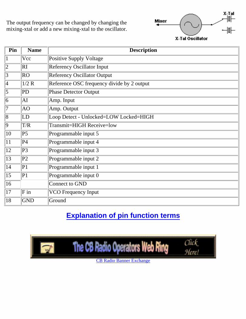
The output frequency can be changed by changing themixing-xtal or add a new mixing-xtal to the oscillator.
Pin Name Description
1 Vcc Positive Supply Voltage
2 RI Referency Oscillator Input
3 RO Referency Oscillator Output
4 1/2 R Reference OSC frequency divide by 2 output
5 PD Phase Detector Output
6 AI Amp. Input
7 AO Amp. Output
8 LD Loop Detect - Unlocked=LOW Locked=HIGH
9 T/R Transmit=HIGH Receive=low
10 P5 Programmable input 5
11 P4 Programmable input 4
12 P3 Programmable input 3
13 P2 Programmable input 2
14 P1 Programmable input 1
15 P1 Programmable input 0
16 Connect to GND
17 F in VCO Frequency Input
18 GND Ground
Explanation of pin function terms
CB Radio Banner Exchange
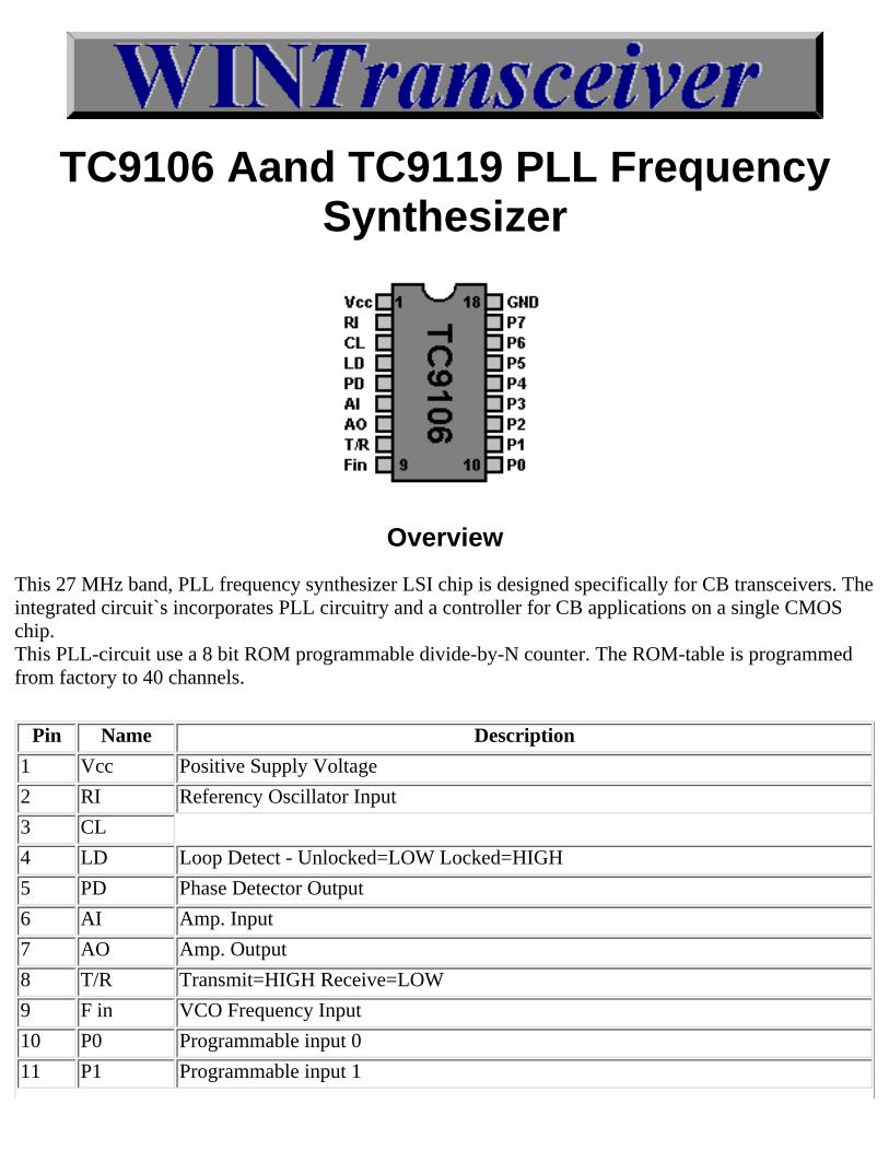
TC9106 Aand TC9119 PLL FrequencySynthesizer
Overview
This 27 MHz band, PLL frequency synthesizer LSI chip is designed specifically for CB transceivers. Theintegrated circuit`s incorporates PLL circuitry and a controller for CB applications on a single CMOSchip.This PLL-circuit use a 8 bit ROM programmable divide-by-N counter. The ROM-table is programmedfrom factory to 40 channels.
Pin Name Description
1 Vcc Positive Supply Voltage
2 RI Referency Oscillator Input
3 CL
4 LD Loop Detect - Unlocked=LOW Locked=HIGH
5 PD Phase Detector Output
6 AI Amp. Input
7 AO Amp. Output
8 T/R Transmit=HIGH Receive=LOW
9 F in VCO Frequency Input
10 P0 Programmable input 0
11 P1 Programmable input 1
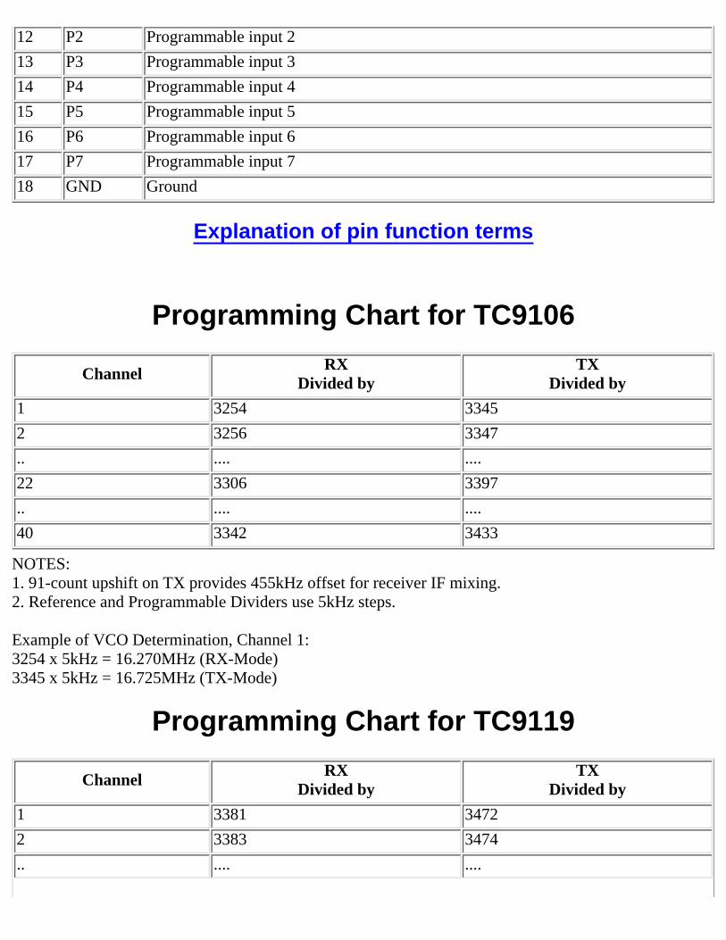
12 P2 Programmable input 2
13 P3 Programmable input 3
14 P4 Programmable input 4
15 P5 Programmable input 5
16 P6 Programmable input 6
17 P7 Programmable input 7
18 GND Ground
Explanation of pin function terms
Programming Chart for TC9106
Channel RXDivided by
TXDivided by
1 3254 3345
2 3256 3347
.. .... ....
22 3306 3397
.. .... ....
40 3342 3433
NOTES:1. 91-count upshift on TX provides 455kHz offset for receiver IF mixing.2. Reference and Programmable Dividers use 5kHz steps.
Example of VCO Determination, Channel 1:3254 x 5kHz = 16.270MHz (RX-Mode)3345 x 5kHz = 16.725MHz (TX-Mode)
Programming Chart for TC9119
Channel RXDivided by
TXDivided by
1 3381 3472
2 3383 3474
.. .... ....
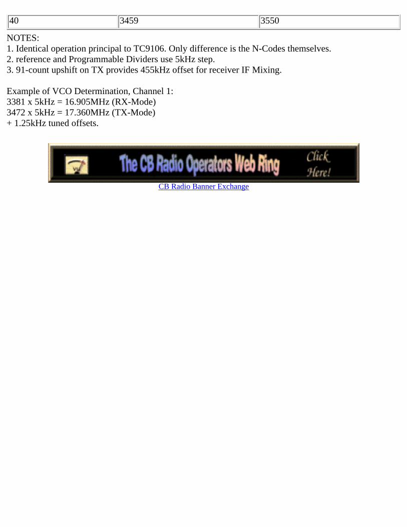
40 3459 3550
NOTES:1. Identical operation principal to TC9106. Only difference is the N-Codes themselves.2. reference and Programmable Dividers use 5kHz step.3. 91-count upshift on TX provides 455kHz offset for receiver IF Mixing.
Example of VCO Determination, Channel 1:3381 x 5kHz = 16.905MHz (RX-Mode)3472 x 5kHz = 17.360MHz (TX-Mode)+ 1.25kHz tuned offsets.
CB Radio Banner Exchange
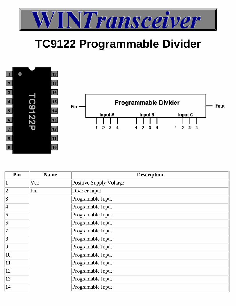
TC9122 Programmable Divider
Pin Name Description
1 Vcc Positive Supply Voltage
2 Fin Divider Input
3 Programable Input
4 Programable Input
5 Programable Input
6 Programable Input
7 Programable Input
8 Programable Input
9 Programable Input
10 Programable Input
11 Programable Input
12 Programable Input
13 Programable Input
14 Programable Input

15 Programable Input
16 Programable Input
17 Fout Divider Output
18 GND Ground
CB Radio Banner Exchange
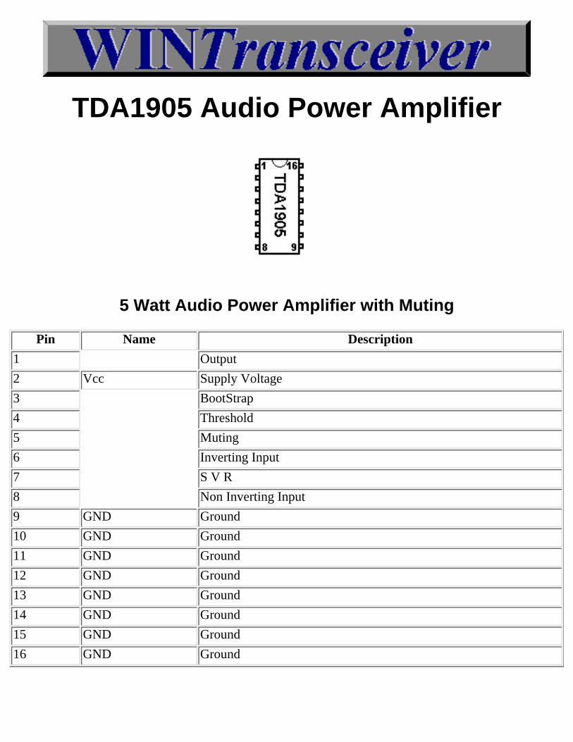
TDA1905 Audio Power Amplifier
5 Watt Audio Power Amplifier with Muting
Pin Name Description
1 Output
2 Vcc Supply Voltage
3 BootStrap
4 Threshold
5 Muting
6 Inverting Input
7 S V R
8 Non Inverting Input
9 GND Ground
10 GND Ground
11 GND Ground
12 GND Ground
13 GND Ground
14 GND Ground
15 GND Ground
16 GND Ground

CB Radio Banner Exchange
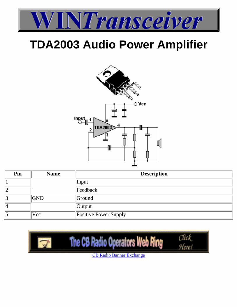
TDA2003 Audio Power Amplifier
Pin Name Description
1 Input
2 Feedback
3 GND Ground
4 Output
5 Vcc Positive Power Supply
CB Radio Banner Exchange
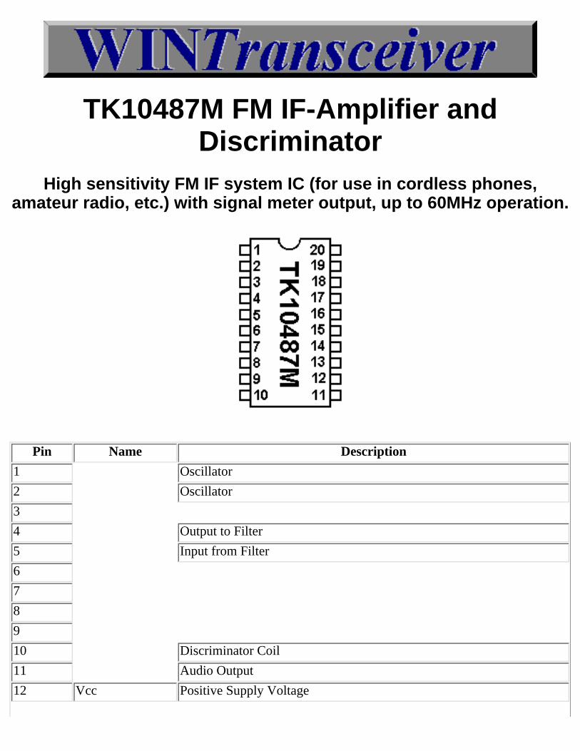
TK10487M FM IF-Amplifier andDiscriminator
High sensitivity FM IF system IC (for use in cordless phones,amateur radio, etc.) with signal meter output, up to 60MHz operation.
Pin Name Description
1 Oscillator
2 Oscillator
3
4 Output to Filter
5 Input from Filter
6
7
8
9
10 Discriminator Coil
11 Audio Output
12 Vcc Positive Supply Voltage
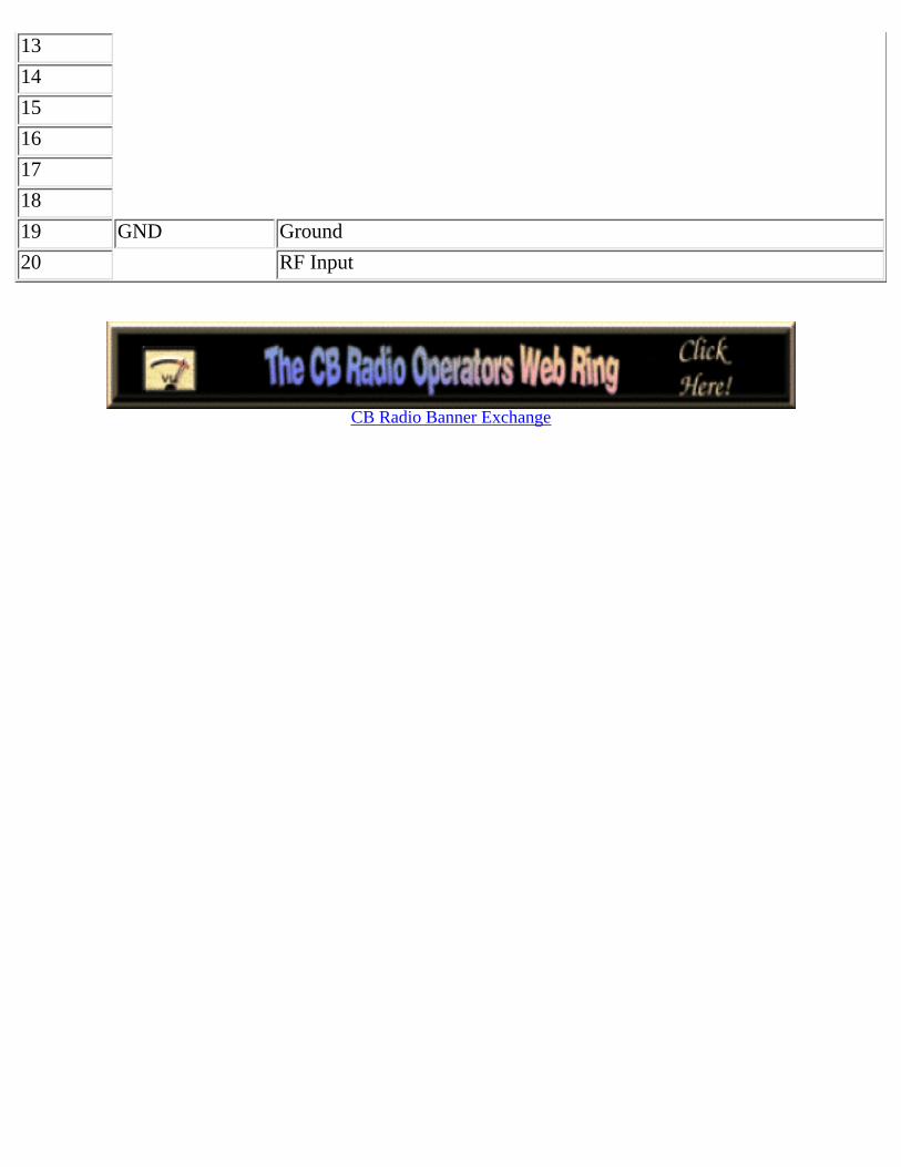
13
14
15
16
17
18
19 GND Ground
20 RF Input
CB Radio Banner Exchange
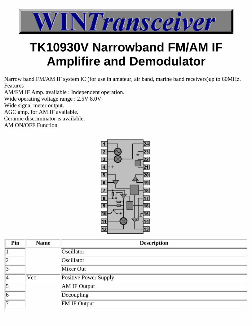
TK10930V Narrowband FM/AM IFAmplifire and Demodulator
Narrow band FM/AM IF system lC (for use in amateur, air band, marine band receivers)up to 60MHz.FeaturesAM/FM IF Amp. available : Independent operation.Wide operating voltage range : 2.5V 8.0V.Wide signal meter output.AGC amp. for AM IF available.Ceramic discriminator is available.AM ON/OFF Function
Pin Name Description
1 Oscillator
2 Oscillator
3 Mixer Out
4 Vcc Positive Power Supply
5 AM IF Output
6 Decoupling
7 FM IF Output
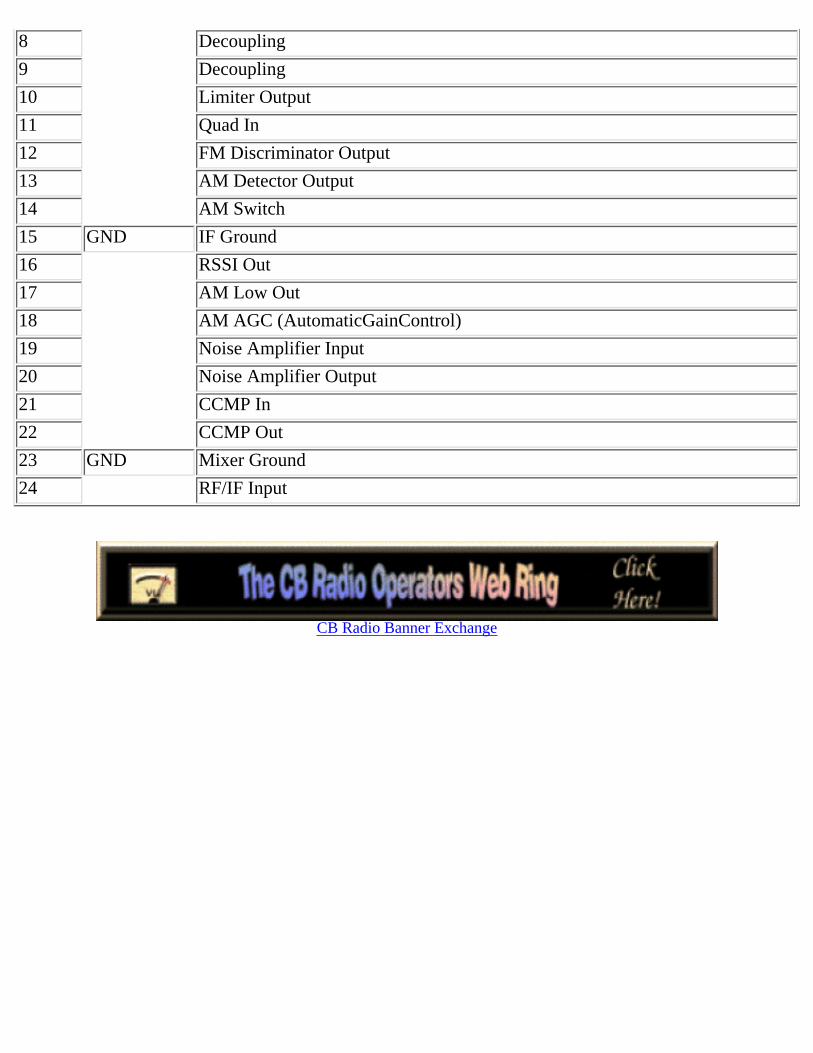
8 Decoupling
9 Decoupling
10 Limiter Output
11 Quad In
12 FM Discriminator Output
13 AM Detector Output
14 AM Switch
15 GND IF Ground
16 RSSI Out
17 AM Low Out
18 AM AGC (AutomaticGainControl)
19 Noise Amplifier Input
20 Noise Amplifier Output
21 CCMP In
22 CCMP Out
23 GND Mixer Ground
24 RF/IF Input
CB Radio Banner Exchange
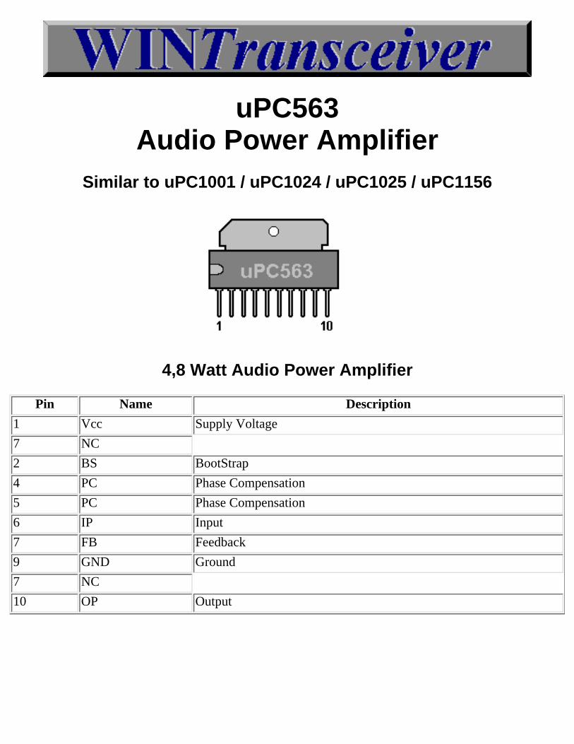
uPC563Audio Power Amplifier
Similar to uPC1001 / uPC1024 / uPC1025 / uPC1156
4,8 Watt Audio Power Amplifier
Pin Name Description
1 Vcc Supply Voltage
7 NC
2 BS BootStrap
4 PC Phase Compensation
5 PC Phase Compensation
6 IP Input
7 FB Feedback
9 GND Ground
7 NC
10 OP Output
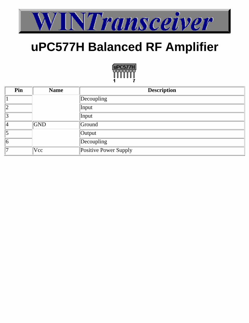
uPC577H Balanced RF Amplifier
Pin Name Description
1 Decoupling
2 Input
3 Input
4 GND Ground
5 Output
6 Decoupling
7 Vcc Positive Power Supply
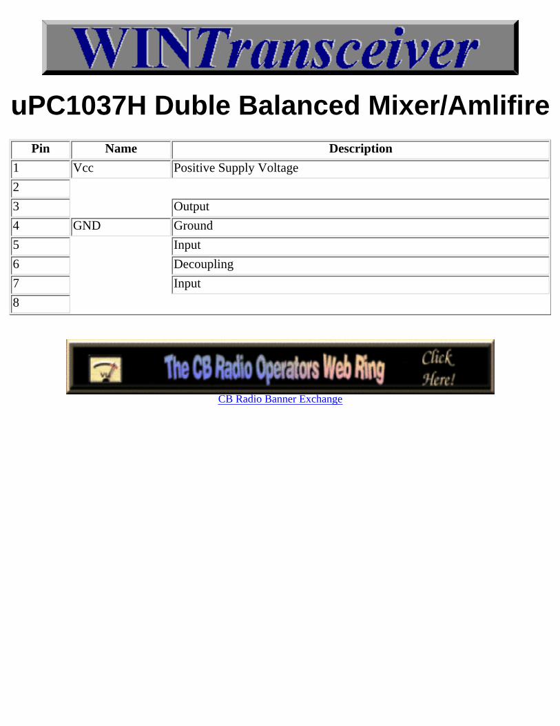
uPC1037H Duble Balanced Mixer/AmlifirePin Name Description
1 Vcc Positive Supply Voltage
2
3 Output
4 GND Ground
5 Input
6 Decoupling
7 Input
8
CB Radio Banner Exchange
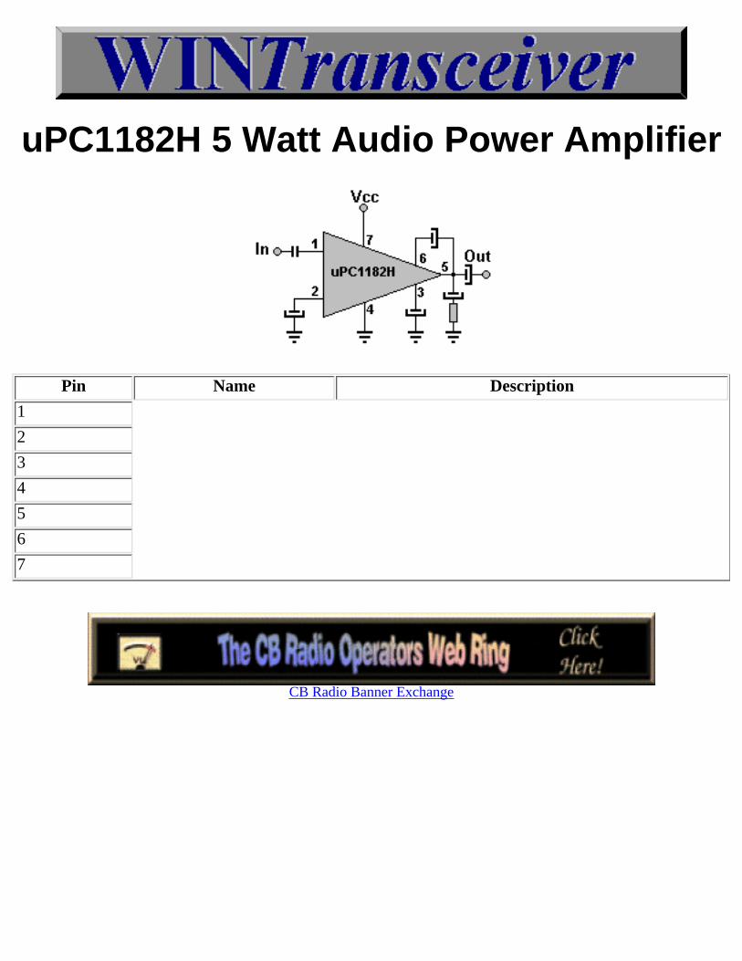
uPC1182H 5 Watt Audio Power Amplifier
Pin Name Description
1
2
3
4
5
6
7
CB Radio Banner Exchange
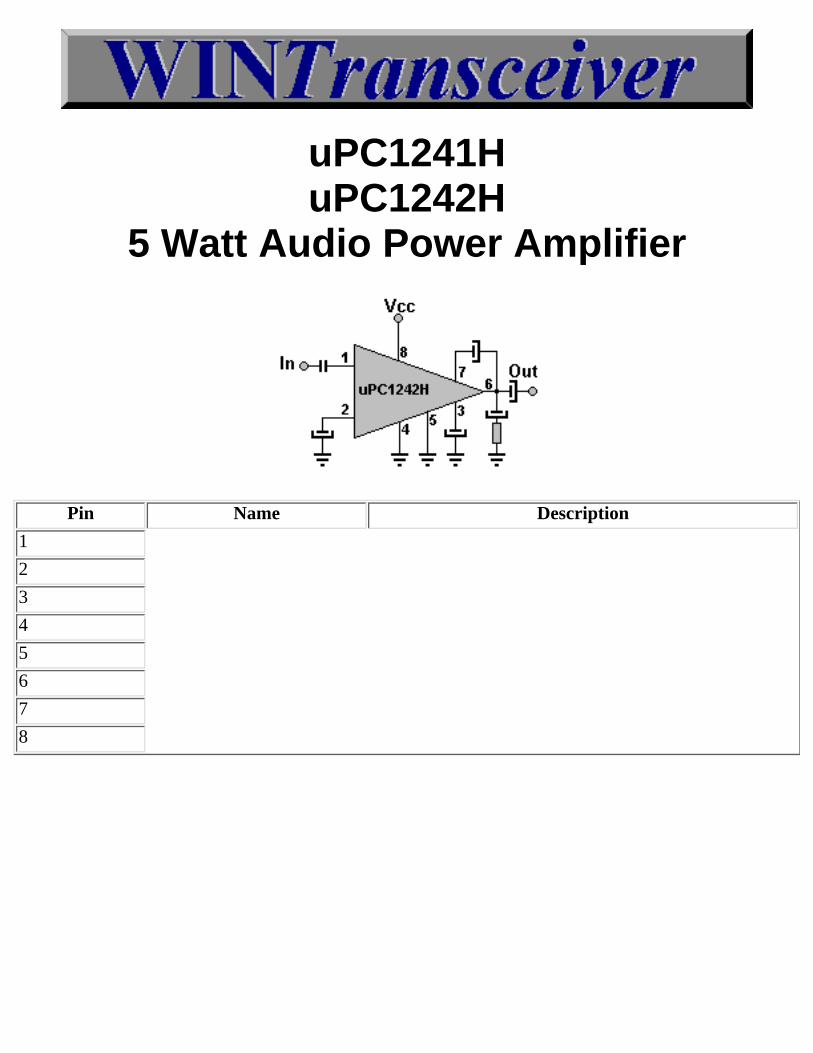
uPC1241HuPC1242H
5 Watt Audio Power Amplifier
Pin Name Description
1
2
3
4
5
6
7
8
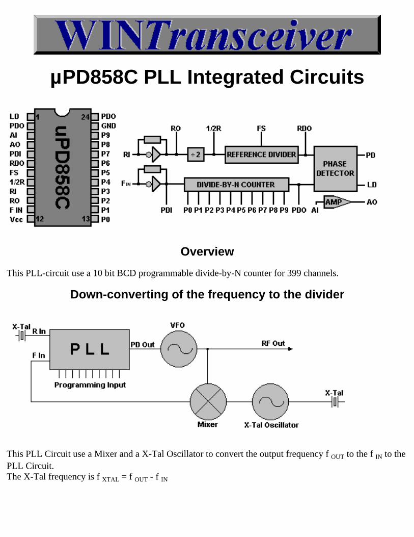
µPD858C PLL Integrated Circuits
Overview
This PLL-circuit use a 10 bit BCD programmable divide-by-N counter for 399 channels.
Down-converting of the frequency to the divider
This PLL Circuit use a Mixer and a X-Tal Oscillator to convert the output frequency f OUT to the f IN to thePLL Circuit.The X-Tal frequency is f XTAL = f OUT - f IN
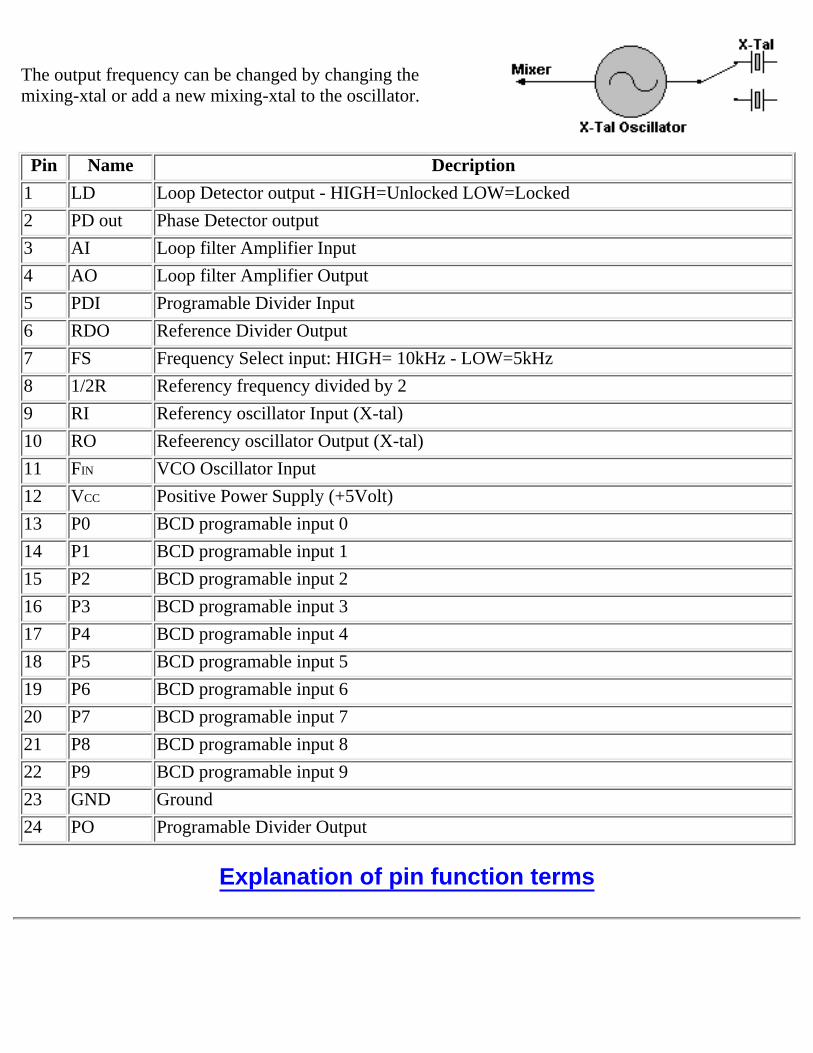
The output frequency can be changed by changing themixing-xtal or add a new mixing-xtal to the oscillator.
Pin Name Decription
1 LD Loop Detector output - HIGH=Unlocked LOW=Locked
2 PD out Phase Detector output
3 AI Loop filter Amplifier Input
4 AO Loop filter Amplifier Output
5 PDI Programable Divider Input
6 RDO Reference Divider Output
7 FS Frequency Select input: HIGH= 10kHz - LOW=5kHz
8 1/2R Referency frequency divided by 2
9 RI Referency oscillator Input (X-tal)
10 RO Refeerency oscillator Output (X-tal)
11 FIN VCO Oscillator Input
12 VCC Positive Power Supply (+5Volt)
13 P0 BCD programable input 0
14 P1 BCD programable input 1
15 P2 BCD programable input 2
16 P3 BCD programable input 3
17 P4 BCD programable input 4
18 P5 BCD programable input 5
19 P6 BCD programable input 6
20 P7 BCD programable input 7
21 P8 BCD programable input 8
22 P9 BCD programable input 9
23 GND Ground
24 PO Programable Divider Output
Explanation of pin function terms
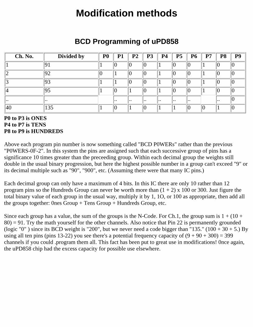
Modification methods
BCD Programming of uPD858
Ch. No. Divided by P0 P1 P2 P3 P4 P5 P6 P7 P8 P9
1 91 1 0 0 0 1 0 0 1 0 0
2 92 0 1 0 0 1 0 0 1 0 0
3 93 1 1 0 0 1 0 0 1 0 0
4 95 1 0 1 0 1 0 0 1 0 0
.. .. .. .. .. .. .. .. .. 0
40 135 1 0 1 0 1 1 0 0 1 0
P0 to P3 is ONESP4 to P7 is TENSP8 to P9 is HUNDREDS
Above each program pin number is now something called "BCD P0WERs" rather than the previous"P0WERS-0F-2". In this system the pins are assigned such that each successive group of pins has asignificance 10 times greater than the preceeding group. Within each decimal group the weights stilldouble in the usual binary progression, but here the highest possible number in a group can't exceed "9" orits decimal multiple such as "90", "900", etc. (Assuming there were that many IC pins.)
Each decimal group can only have a maximum of 4 bits. In this IC there are only 10 rather than 12program pins so the Hundreds Group can never be worth more than (1 + 2) x 100 or 300. Just figure thetotal binary value of each group in the usual way, multiply it by 1, 1O, or 100 as appropriate, then add allthe groups together: 0nes Group + Tens Group + Hundreds Group, etc.
Since each group has a value, the sum of the groups is the N-Code. For Ch.1, the group sum is 1 + (10 +80) = 91. Try the math yourself for the other channels. Also notice that Pin 22 is permanently grounded(logic "0" ) since its BCD weight is "200", but we never need a code bigger than "135." (100 + 30 + 5.) Byusing all ten pins (pins 13-22) you see there's a potential frequency capacity of (9 + 90 + 300) = 399channels if you could .program them all. This fact has been put to great use in modifications! 0nce again,the uPD858 chip had the excess capacity for possible use elsewhere.
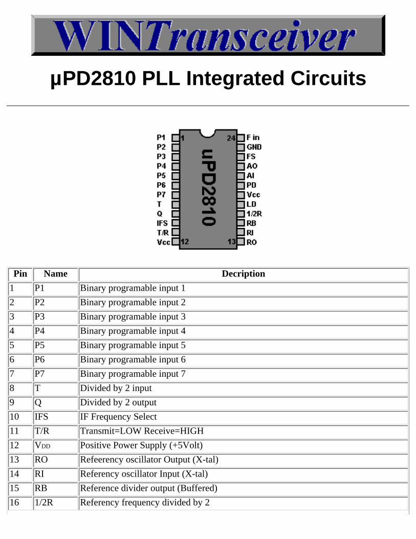
µPD2810 PLL Integrated Circuits
Pin Name Decription
1 P1 Binary programable input 1
2 P2 Binary programable input 2
3 P3 Binary programable input 3
4 P4 Binary programable input 4
5 P5 Binary programable input 5
6 P6 Binary programable input 6
7 P7 Binary programable input 7
8 T Divided by 2 input
9 Q Divided by 2 output
10 IFS IF Frequency Select
11 T/R Transmit=LOW Receive=HIGH
12 VDD Positive Power Supply (+5Volt)
13 RO Refeerency oscillator Output (X-tal)
14 RI Referency oscillator Input (X-tal)
15 RB Reference divider output (Buffered)
16 1/2R Referency frequency divided by 2
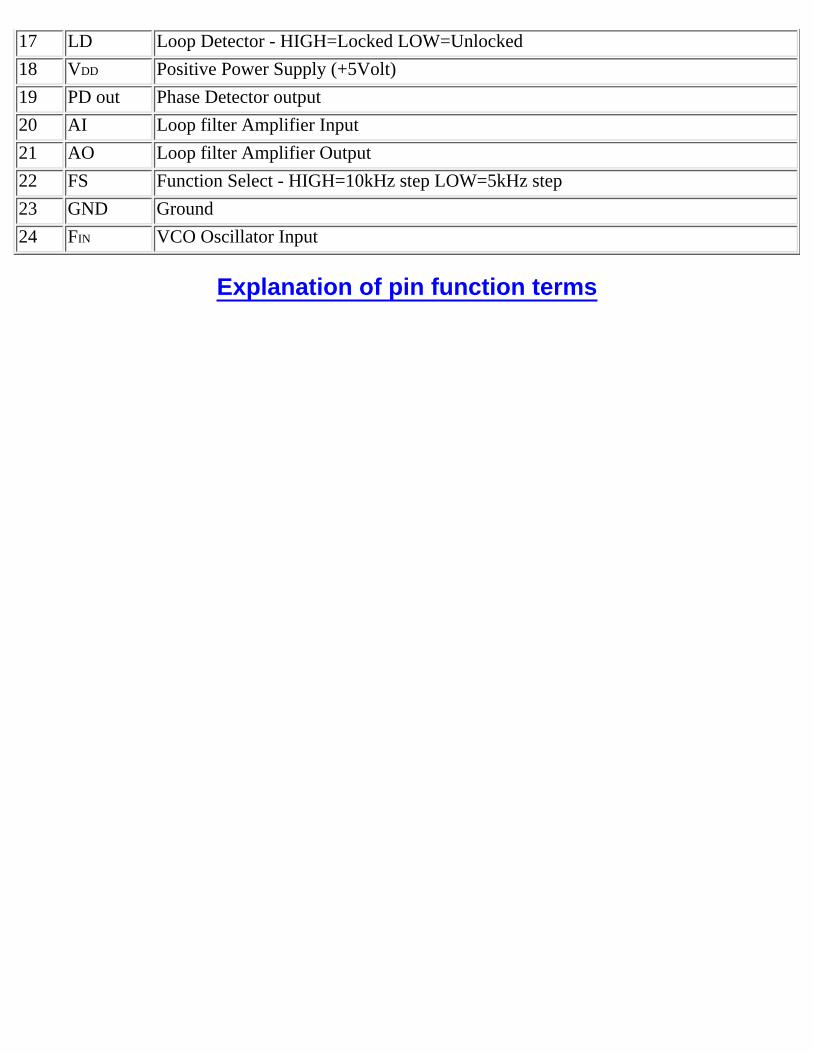
17 LD Loop Detector - HIGH=Locked LOW=Unlocked
18 VDD Positive Power Supply (+5Volt)
19 PD out Phase Detector output
20 AI Loop filter Amplifier Input
21 AO Loop filter Amplifier Output
22 FS Function Select - HIGH=10kHz step LOW=5kHz step
23 GND Ground
24 FIN VCO Oscillator Input
Explanation of pin function terms
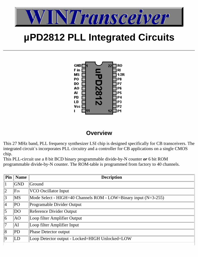
µPD2812 PLL Integrated Circuits
Overview
This 27 MHz band, PLL frequency synthesizer LSI chip is designed specifically for CB transceivers. Theintegrated circuit`s incorporates PLL circuitry and a controller for CB applications on a single CMOSchip.This PLL-circuit use a 8 bit BCD binary programmable divide-by-N counter or 6 bit ROMprogrammable divide-by-N counter. The ROM-table is programmed from factory to 40 channels.
Pin Name Decription
1 GND Ground
2 FIN VCO Oscillator Input
3 MS Mode Select - HIGH=40 Channels ROM - LOW=Binary input (N=3-255)
4 PO Programable Divider Output
5 DO Reference Divider Output
6 AO Loop filter Amplifier Output
7 AI Loop filter Amplifier Input
8 PD Phase Detector output
9 LD Loop Detector output - Locked=HIGH Unlocked=LOW
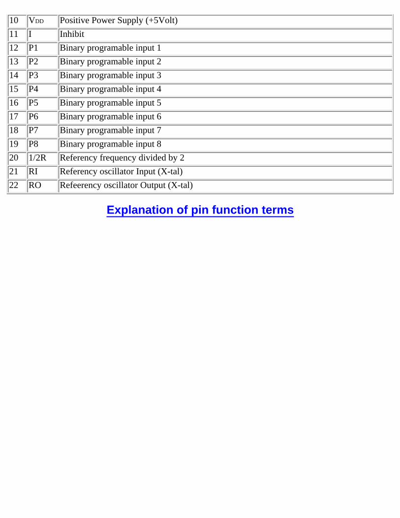
10 VDD Positive Power Supply (+5Volt)
11 I Inhibit
12 P1 Binary programable input 1
13 P2 Binary programable input 2
14 P3 Binary programable input 3
15 P4 Binary programable input 4
16 P5 Binary programable input 5
17 P6 Binary programable input 6
18 P7 Binary programable input 7
19 P8 Binary programable input 8
20 1/2R Referency frequency divided by 2
21 RI Referency oscillator Input (X-tal)
22 RO Refeerency oscillator Output (X-tal)
Explanation of pin function terms
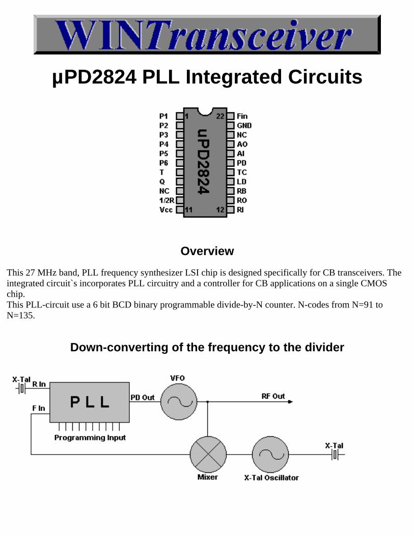
µPD2824 PLL Integrated Circuits
Overview
This 27 MHz band, PLL frequency synthesizer LSI chip is designed specifically for CB transceivers. Theintegrated circuit`s incorporates PLL circuitry and a controller for CB applications on a single CMOSchip.This PLL-circuit use a 6 bit BCD binary programmable divide-by-N counter. N-codes from N=91 toN=135.
Down-converting of the frequency to the divider
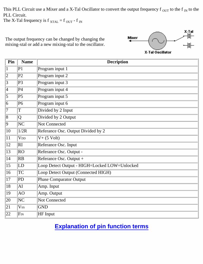
This PLL Circuit use a Mixer and a X-Tal Oscillator to convert the output frequency f OUT to the f IN to thePLL Circuit.The X-Tal frequency is f XTAL = f OUT - f IN
The output frequency can be changed by changing themixing-xtal or add a new mixing-xtal to the oscillator.
Pin Name Decription
1 P1 Program input 1
2 P2 Program input 2
3 P3 Program input 3
4 P4 Program input 4
5 P5 Program input 5
6 P6 Program input 6
7 T Divided by 2 Input
8 Q Divided by 2 Output
9 NC Not Connected
10 1/2R Referance Osc. Output Divided by 2
11 VDD V+ (5 Volt)
12 RI Referance Osc. Input
13 RO Referance Osc. Output -
14 RB Referance Osc. Output +
15 LD Loop Detect Output - HIGH=Locked LOW=Unlocked
16 TC Loop Detect Output (Connected HIGH)
17 PD Phase Comparator Output
18 AI Amp. Input
19 AO Amp. Output
20 NC Not Connected
21 VSS GND
22 FIN HF Input
Explanation of pin function terms
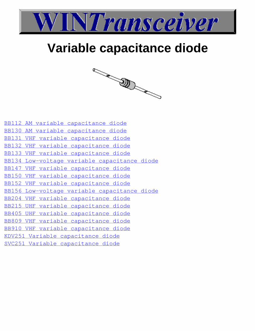
Variable capacitance diode
BB112 AM variable capacitance diodeBB130 AM variable capacitance diodeBB131 VHF variable capacitance diodeBB132 VHF variable capacitance diodeBB133 VHF variable capacitance diodeBB134 Low-voltage variable capacitance diodeBB147 VHF variable capacitance diodeBB150 VHF variable capacitance diodeBB152 VHF variable capacitance diodeBB156 Low-voltage variable capacitance diodeBB204 VHF variable capacitance diodeBB215 UHF variable capacitance diodeBB405 UHF variable capacitance diodeBB809 VHF variable capacitance diodeBB910 VHF variable capacitance diodeKDV251 Variable capacitance diodeSVC251 Variable capacitance diode
CB Radio BannerExchange
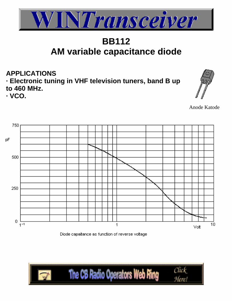
BB112AM variable capacitance diode
APPLICATIONS· Electronic tuning in VHF television tuners, band B upto 460 MHz.· VCO.
Anode Katode
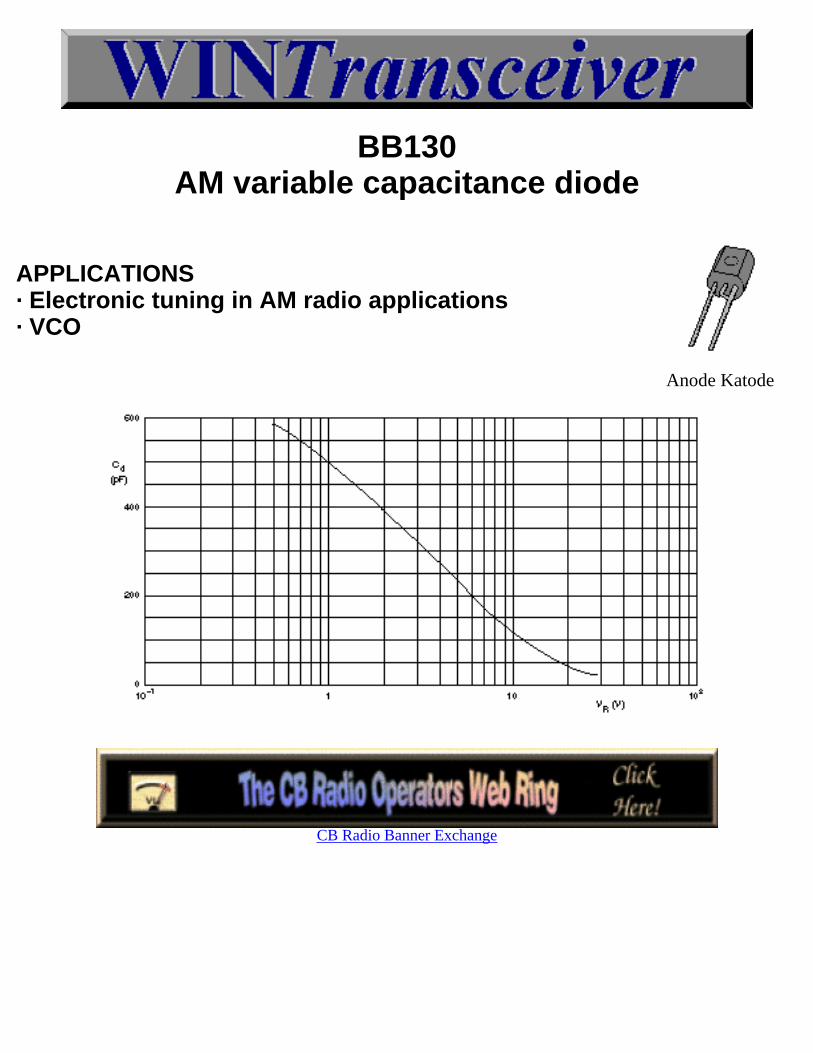
BB130AM variable capacitance diode
APPLICATIONS· Electronic tuning in AM radio applications· VCO
Anode Katode
CB Radio Banner Exchange
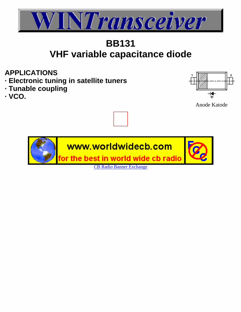
BB131VHF variable capacitance diode
APPLICATIONS· Electronic tuning in satellite tuners· Tunable coupling· VCO.
Anode Katode
CB Radio Banner Exchange
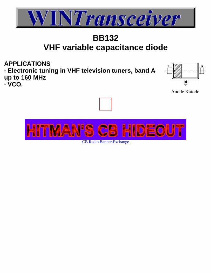
BB132VHF variable capacitance diode
APPLICATIONS· Electronic tuning in VHF television tuners, band Aup to 160 MHz· VCO.
Anode Katode
CB Radio Banner Exchange
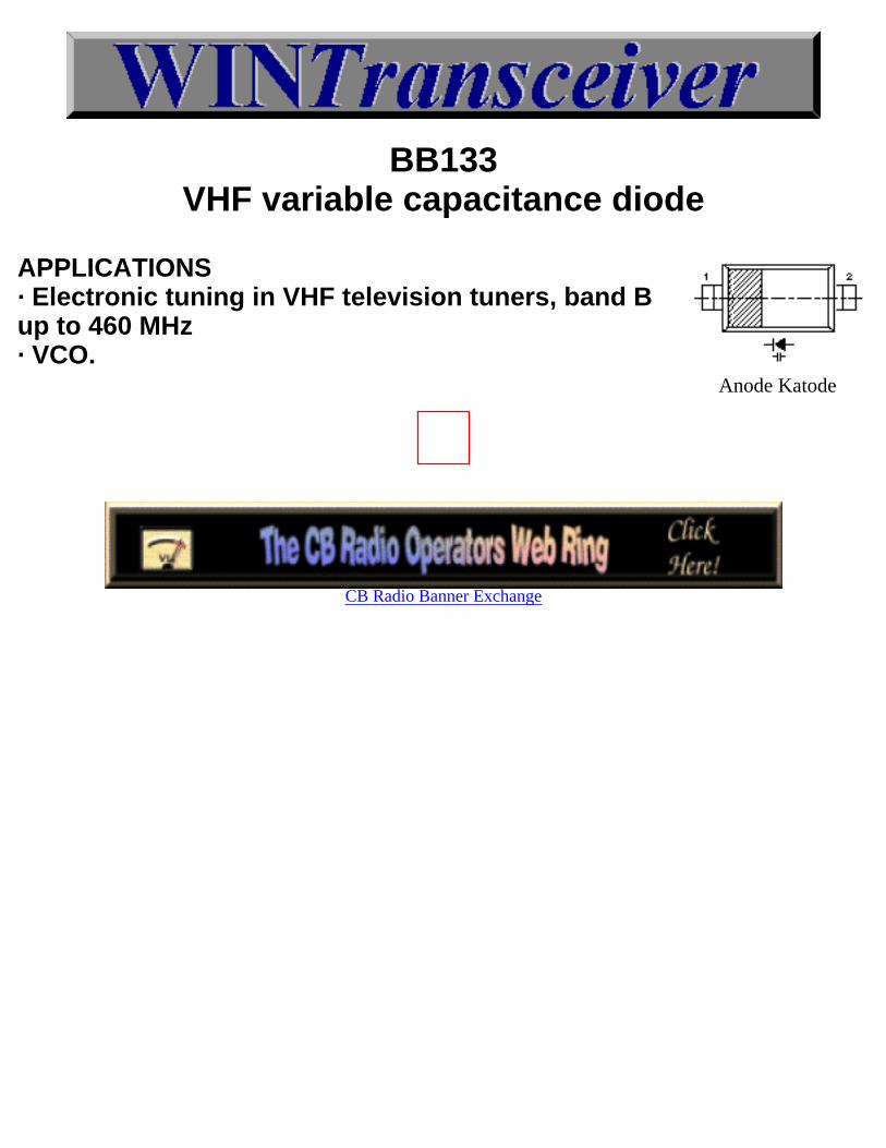
BB133VHF variable capacitance diode
APPLICATIONS· Electronic tuning in VHF television tuners, band Bup to 460 MHz· VCO.
Anode Katode
CB Radio Banner Exchange
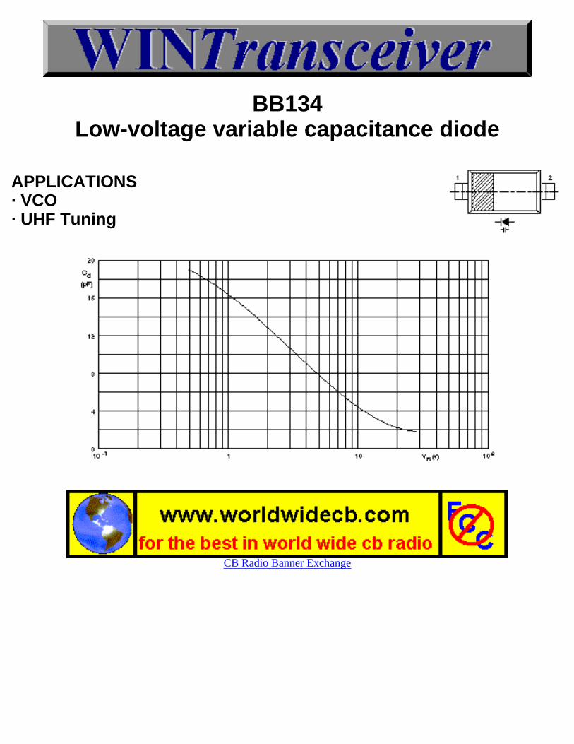
BB134Low-voltage variable capacitance diode
APPLICATIONS· VCO· UHF Tuning
CB Radio Banner Exchange
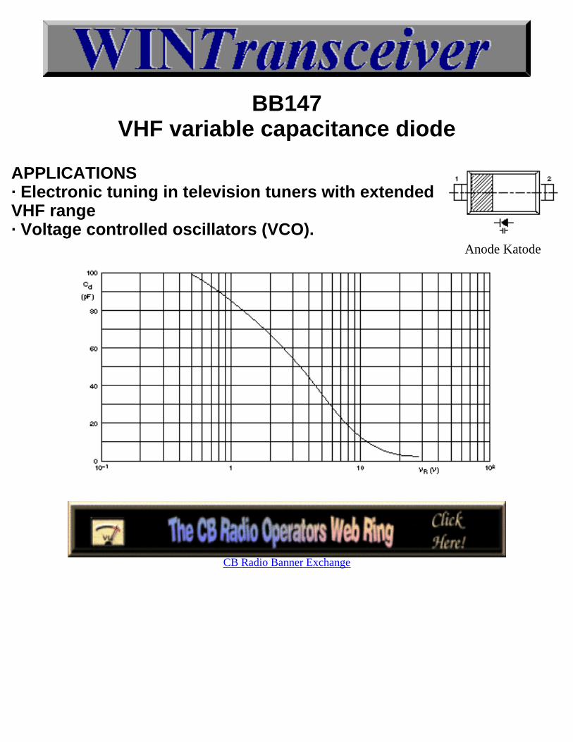
BB147VHF variable capacitance diode
APPLICATIONS· Electronic tuning in television tuners with extendedVHF range· Voltage controlled oscillators (VCO).
Anode Katode
CB Radio Banner Exchange
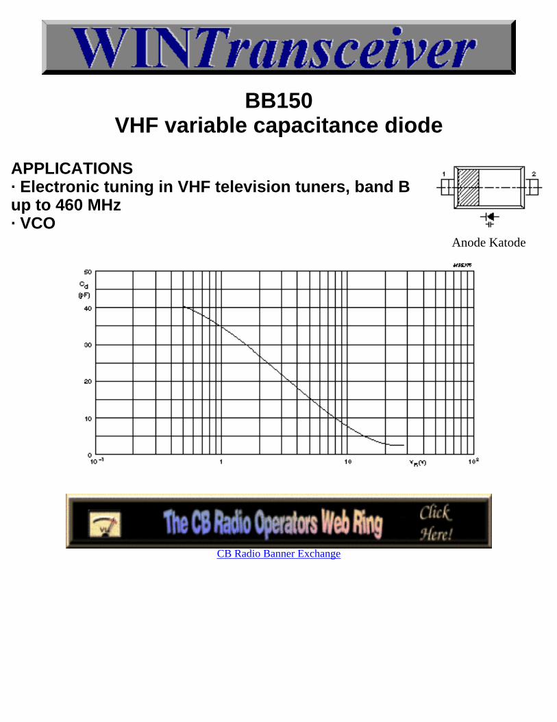
BB150VHF variable capacitance diode
APPLICATIONS· Electronic tuning in VHF television tuners, band Bup to 460 MHz· VCO
Anode Katode
CB Radio Banner Exchange
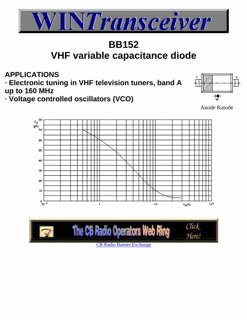
BB152VHF variable capacitance diode
APPLICATIONS· Electronic tuning in VHF television tuners, band Aup to 160 MHz· Voltage controlled oscillators (VCO)
Anode Katode
CB Radio Banner Exchange
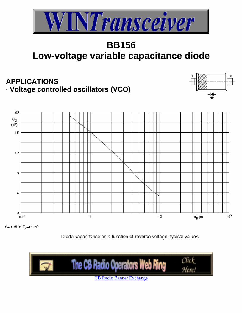
BB156Low-voltage variable capacitance diode
APPLICATIONS· Voltage controlled oscillators (VCO)
CB Radio Banner Exchange
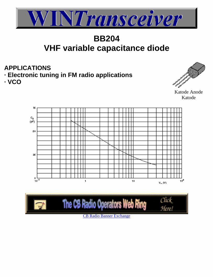
BB204VHF variable capacitance diode
APPLICATIONS· Electronic tuning in FM radio applications· VCO
Katode AnodeKatode
CB Radio Banner Exchange
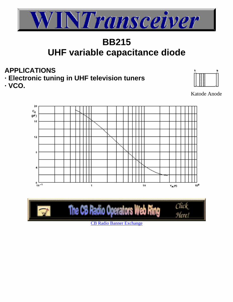
BB215UHF variable capacitance diode
APPLICATIONS· Electronic tuning in UHF television tuners· VCO.
Katode Anode
CB Radio Banner Exchange
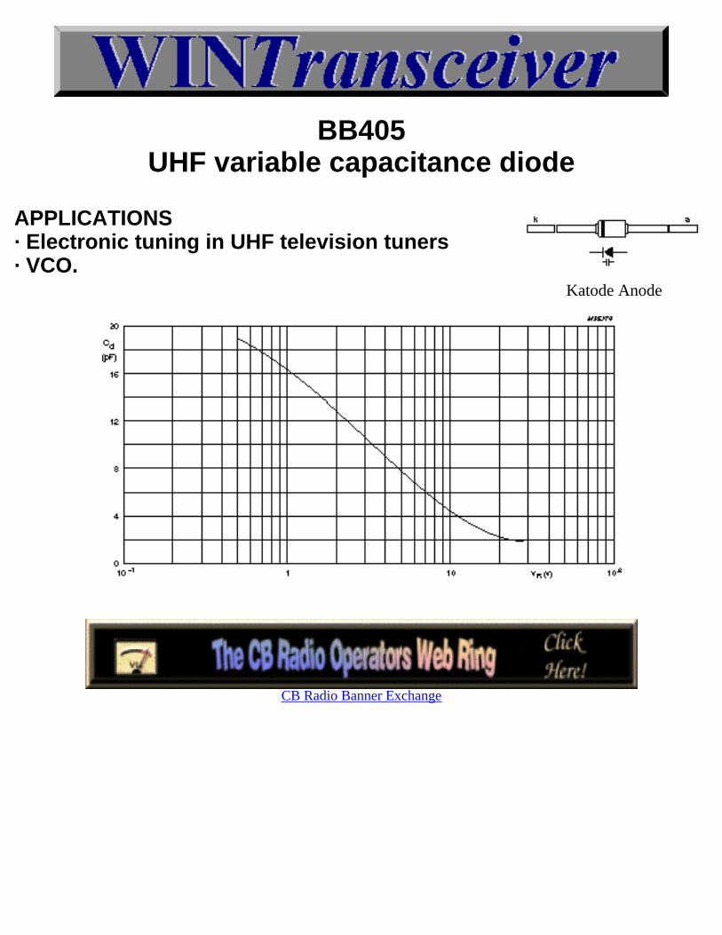
BB405UHF variable capacitance diode
APPLICATIONS· Electronic tuning in UHF television tuners· VCO.
Katode Anode
CB Radio Banner Exchange
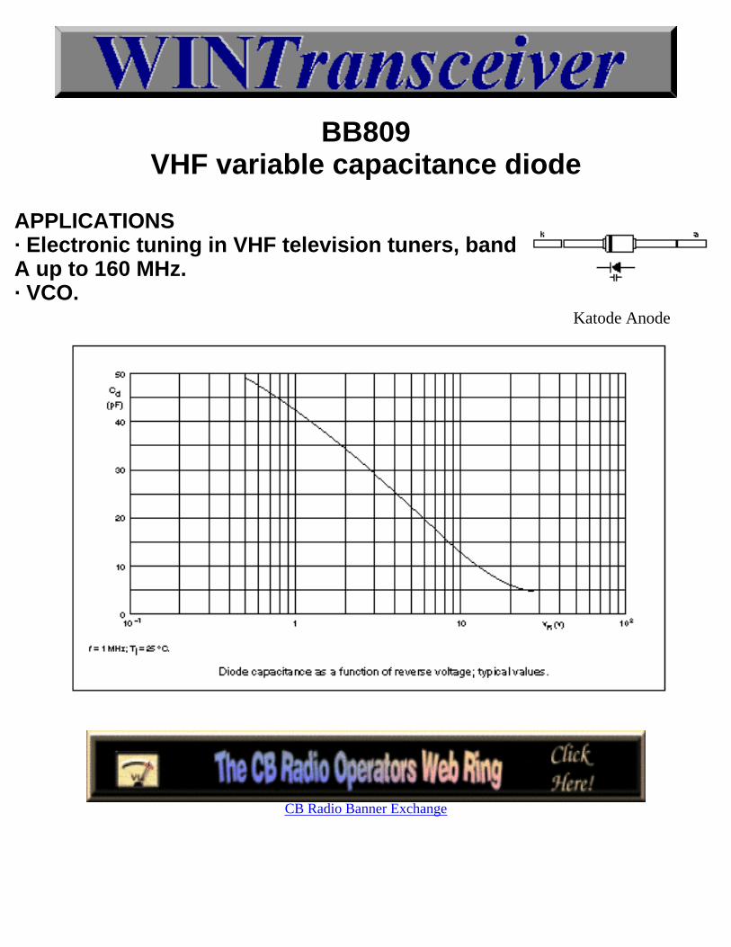
BB809VHF variable capacitance diode
APPLICATIONS· Electronic tuning in VHF television tuners, bandA up to 160 MHz.· VCO.
Katode Anode
CB Radio Banner Exchange
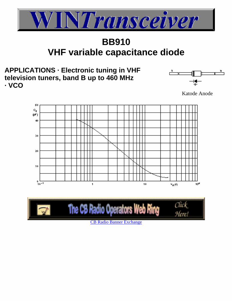
BB910VHF variable capacitance diode
APPLICATIONS · Electronic tuning in VHFtelevision tuners, band B up to 460 MHz· VCO
Katode Anode
CB Radio Banner Exchange
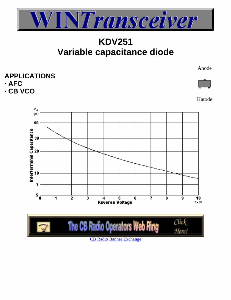
KDV251Variable capacitance diode
Anode
APPLICATIONS· AFC· CB VCO
Katode
CB Radio Banner Exchange
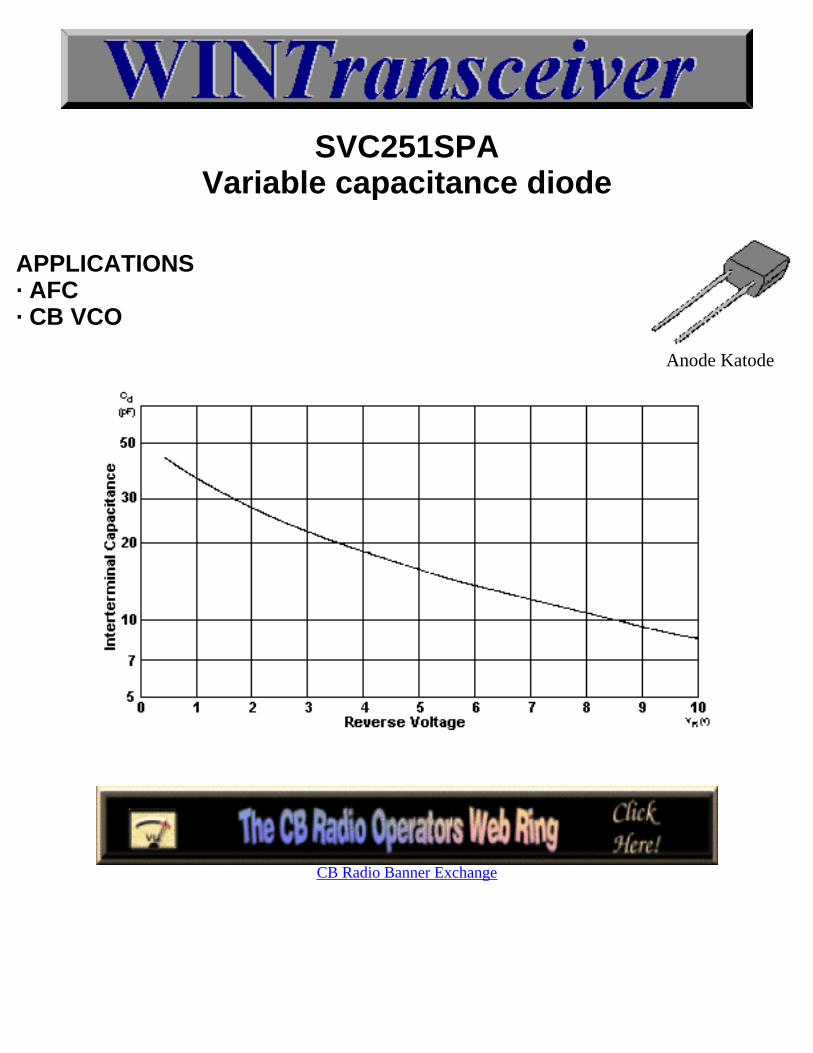
SVC251SPAVariable capacitance diode
APPLICATIONS· AFC· CB VCO
Anode Katode
CB Radio Banner Exchange
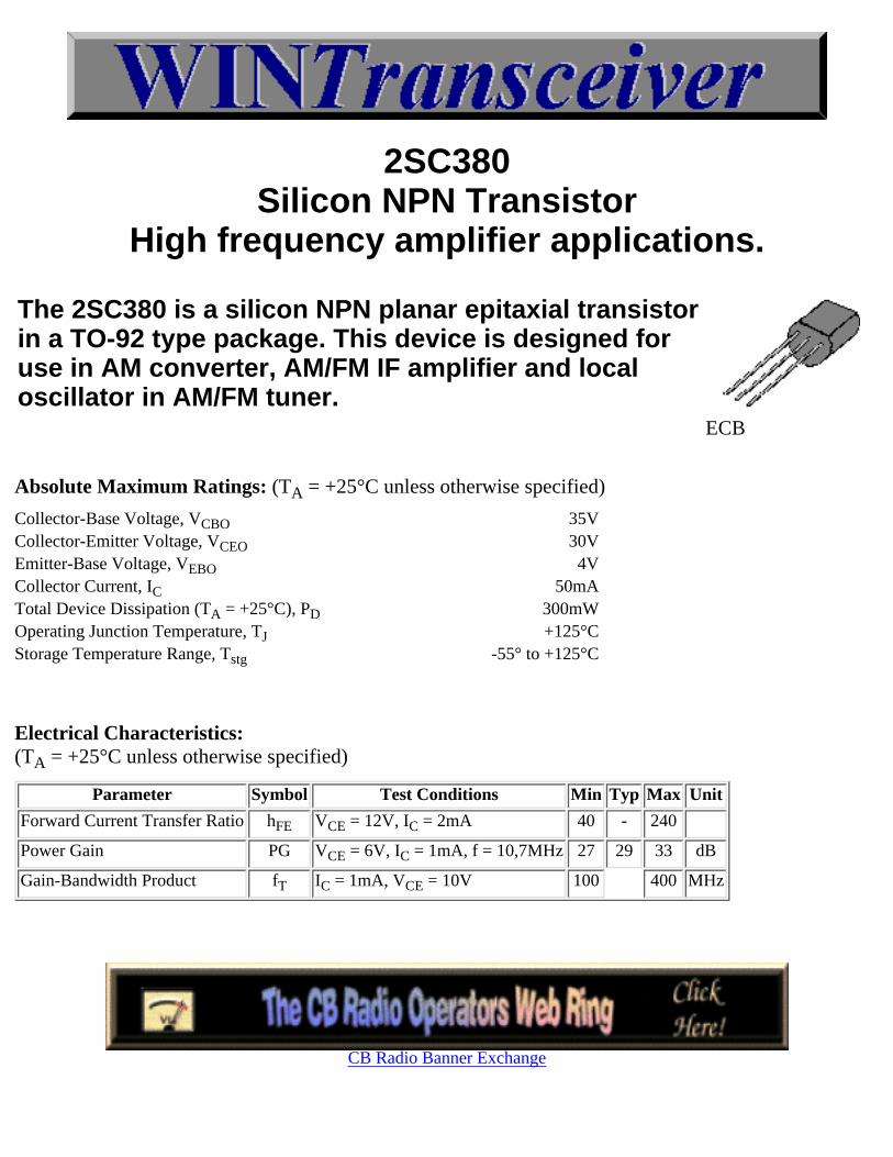
2SC380Silicon NPN Transistor
High frequency amplifier applications.
The 2SC380 is a silicon NPN planar epitaxial transistorin a TO-92 type package. This device is designed foruse in AM converter, AM/FM IF amplifier and localoscillator in AM/FM tuner.
ECB
Absolute Maximum Ratings: (TA = +25°C unless otherwise specified)
Collector-Base Voltage, VCBO 35VCollector-Emitter Voltage, VCEO 30VEmitter-Base Voltage, VEBO 4VCollector Current, IC 50mATotal Device Dissipation (TA = +25°C), PD 300mWOperating Junction Temperature, TJ +125°CStorage Temperature Range, Tstg -55° to +125°C
Electrical Characteristics:(TA = +25°C unless otherwise specified)
Parameter Symbol Test Conditions Min Typ Max Unit
Forward Current Transfer Ratio hFE VCE = 12V, IC = 2mA 40 - 240
Power Gain PG VCE = 6V, IC = 1mA, f = 10,7MHz 27 29 33 dB
Gain-Bandwidth Product fT IC = 1mA, VCE = 10V 100 400 MHz
CB Radio Banner Exchange
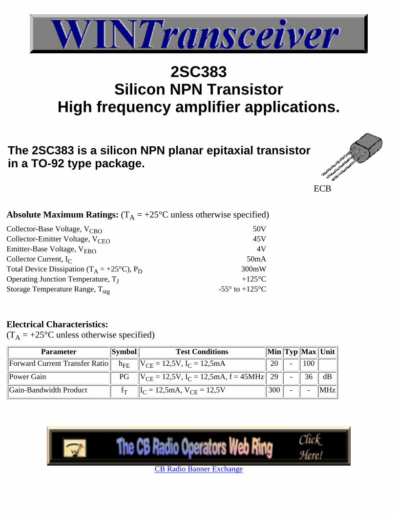
2SC383Silicon NPN Transistor
High frequency amplifier applications.
The 2SC383 is a silicon NPN planar epitaxial transistorin a TO-92 type package.
ECB
Absolute Maximum Ratings: (TA = +25°C unless otherwise specified)
Collector-Base Voltage, VCBO 50VCollector-Emitter Voltage, VCEO 45VEmitter-Base Voltage, VEBO 4VCollector Current, IC 50mATotal Device Dissipation (TA = +25°C), PD 300mWOperating Junction Temperature, TJ +125°CStorage Temperature Range, Tstg -55° to +125°C
Electrical Characteristics:(TA = +25°C unless otherwise specified)
Parameter Symbol Test Conditions Min Typ Max Unit
Forward Current Transfer Ratio hFE VCE = 12,5V, IC = 12,5mA 20 - 100
Power Gain PG VCE = 12,5V, IC = 12,5mA, f = 45MHz 29 - 36 dB
Gain-Bandwidth Product fT IC = 12,5mA, VCE = 12,5V 300 - - MHz
CB Radio Banner Exchange

2SC388Silicon NPN Transistor
High frequency amplifier applications.
The 2SC388 is a silicon NPN planar epitaxial transistorin a TO-92 type package.
ECB
Absolute Maximum Ratings: (TA = +25°C unless otherwise specified)
Collector-Base Voltage, VCBO 30VCollector-Emitter Voltage, VCEO 25VEmitter-Base Voltage, VEBO 4VCollector Current, IC 50mATotal Device Dissipation (TA = +25°C), PD 300mWOperating Junction Temperature, TJ +125°CStorage Temperature Range, Tstg -55° to +125°C
Electrical Characteristics:(TA = +25°C unless otherwise specified)
Parameter Symbol Test Conditions Min Typ Max Unit
Forward Current Transfer Ratio hFE VCE = 12,5V, IC = 12,5mA 20 - 200
Power Gain PG VCE = 12,5V, IC = 12,5mA, f = 45MHz 28 - 36 dB
Gain-Bandwidth Product fT IC = 12,5mA, VCE = 12,5V 300 - - MHz
CB Radio Banner Exchange
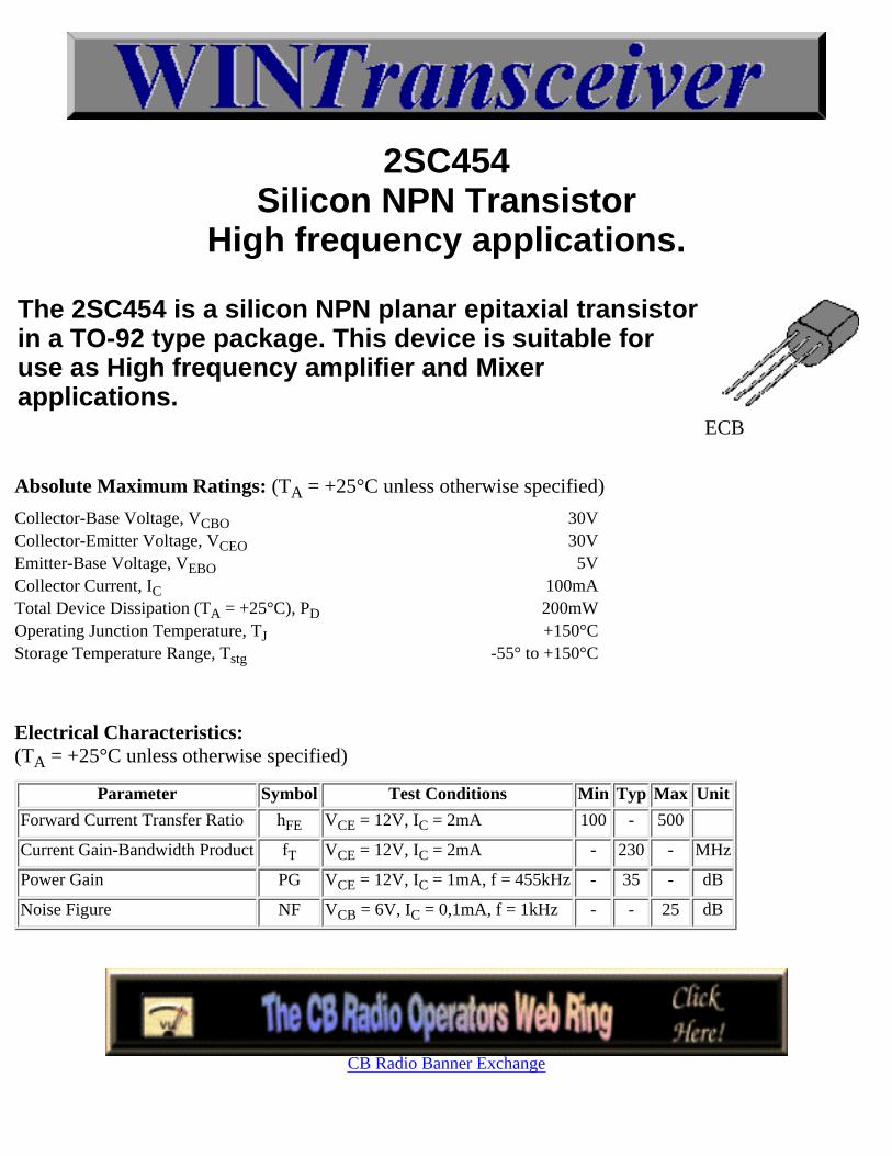
2SC454Silicon NPN Transistor
High frequency applications.
The 2SC454 is a silicon NPN planar epitaxial transistorin a TO-92 type package. This device is suitable foruse as High frequency amplifier and Mixerapplications.
ECB
Absolute Maximum Ratings: (TA = +25°C unless otherwise specified)
Collector-Base Voltage, VCBO 30VCollector-Emitter Voltage, VCEO 30VEmitter-Base Voltage, VEBO 5VCollector Current, IC 100mATotal Device Dissipation (TA = +25°C), PD 200mWOperating Junction Temperature, TJ +150°CStorage Temperature Range, Tstg -55° to +150°C
Electrical Characteristics:(TA = +25°C unless otherwise specified)
Parameter Symbol Test Conditions Min Typ Max Unit
Forward Current Transfer Ratio hFE VCE = 12V, IC = 2mA 100 - 500
Current Gain-Bandwidth Product fT VCE = 12V, IC = 2mA - 230 - MHz
Power Gain PG VCE = 12V, IC = 1mA, f = 455kHz - 35 - dB
Noise Figure NF VCB = 6V, IC = 0,1mA, f = 1kHz - - 25 dB
CB Radio Banner Exchange


2SC460Silicon NPN Transistor
High frequency applications.
The 2SC460 is a silicon NPN planar epitaxial transistorin a TO-92 type package. This device is suitable foruse as High frequency amplifier and Mixerapplications.
ECB
Absolute Maximum Ratings: (TA = +25°C unless otherwise specified)
Collector-Base Voltage, VCBO 30VCollector-Emitter Voltage, VCEO 30VEmitter-Base Voltage, VEBO 5VCollector Current, IC 100mATotal Device Dissipation (TA = +25°C), PD 200mWOperating Junction Temperature, TJ +150°CStorage Temperature Range, Tstg -55° to +150°C
Electrical Characteristics:(TA = +25°C unless otherwise specified)
Parameter Symbol Test Conditions Min Typ Max Unit
Forward Current Transfer Ratio hFE VCE = 12V, IC = 2mA 35 - 200
Current Gain-Bandwidth Product fT VCE = 12V, IC = 2mA - 230 - MHz
Power Gain PG VCE = 6V, IC = 1mA, f = 10,7MHz 26 29 - dB
Noise Figure NF VCB = 6V, IC = 2mA, f = 1MHz - 5 - dB
CB Radio Banner Exchange

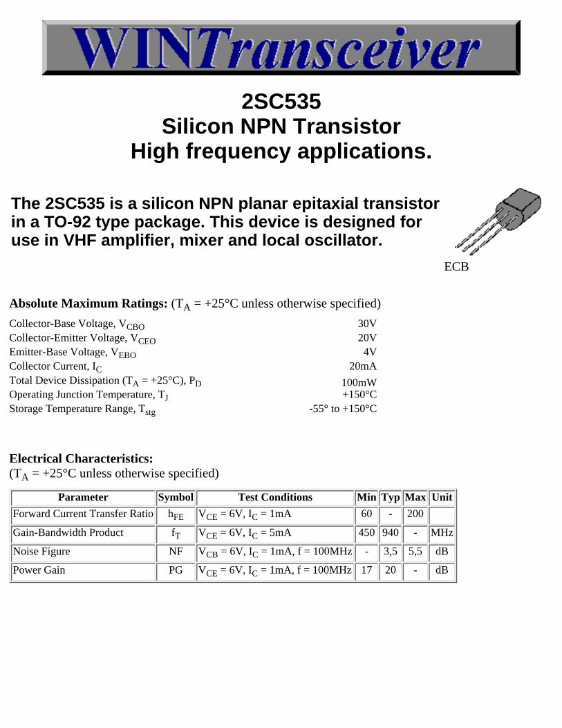
2SC535Silicon NPN Transistor
High frequency applications.
The 2SC535 is a silicon NPN planar epitaxial transistorin a TO-92 type package. This device is designed foruse in VHF amplifier, mixer and local oscillator.
ECB
Absolute Maximum Ratings: (TA = +25°C unless otherwise specified)
Collector-Base Voltage, VCBO 30VCollector-Emitter Voltage, VCEO 20VEmitter-Base Voltage, VEBO 4VCollector Current, IC 20mATotal Device Dissipation (TA = +25°C), PD 100mWOperating Junction Temperature, TJ +150°CStorage Temperature Range, Tstg -55° to +150°C
Electrical Characteristics:(TA = +25°C unless otherwise specified)
Parameter Symbol Test Conditions Min Typ Max Unit
Forward Current Transfer Ratio hFE VCE = 6V, IC = 1mA 60 - 200
Gain-Bandwidth Product fT VCE = 6V, IC = 5mA 450 940 - MHz
Noise Figure NF VCB = 6V, IC = 1mA, f = 100MHz - 3,5 5,5 dB
Power Gain PG VCE = 6V, IC = 1mA, f = 100MHz 17 20 - dB
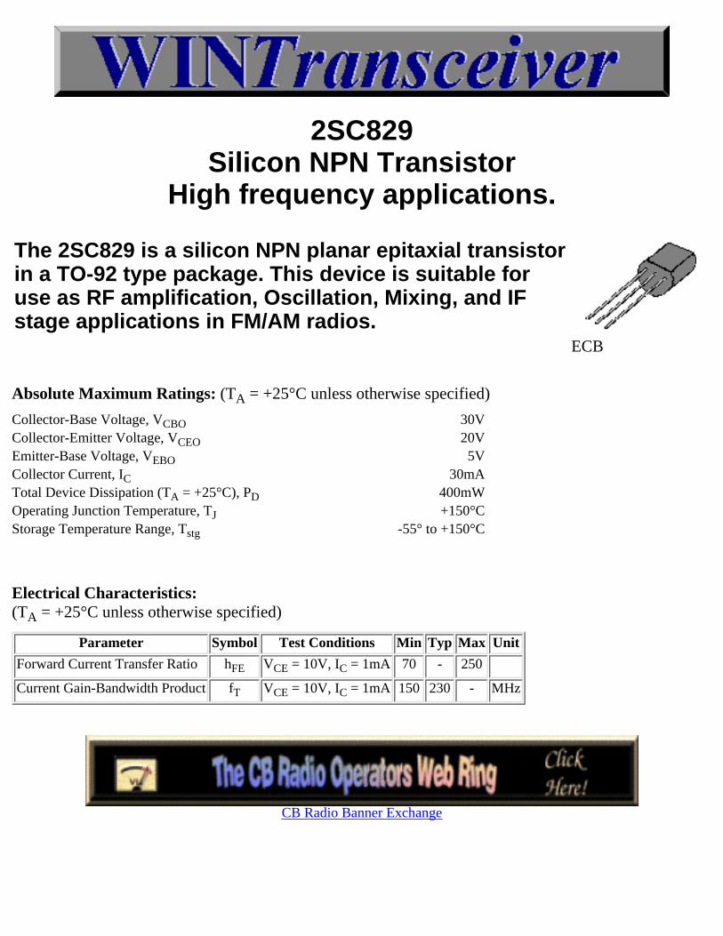
2SC829Silicon NPN Transistor
High frequency applications.
The 2SC829 is a silicon NPN planar epitaxial transistorin a TO-92 type package. This device is suitable foruse as RF amplification, Oscillation, Mixing, and IFstage applications in FM/AM radios.
ECB
Absolute Maximum Ratings: (TA = +25°C unless otherwise specified)
Collector-Base Voltage, VCBO 30VCollector-Emitter Voltage, VCEO 20VEmitter-Base Voltage, VEBO 5VCollector Current, IC 30mATotal Device Dissipation (TA = +25°C), PD 400mWOperating Junction Temperature, TJ +150°CStorage Temperature Range, Tstg -55° to +150°C
Electrical Characteristics:(TA = +25°C unless otherwise specified)
Parameter Symbol Test Conditions Min Typ Max Unit
Forward Current Transfer Ratio hFE VCE = 10V, IC = 1mA 70 - 250
Current Gain-Bandwidth Product fT VCE = 10V, IC = 1mA 150 230 - MHz
CB Radio Banner Exchange
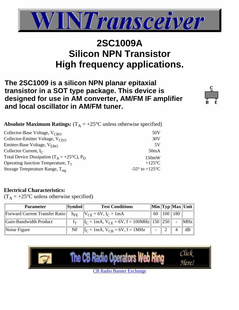
2SC1009ASilicon NPN Transistor
High frequency applications.
The 2SC1009 is a silicon NPN planar epitaxialtransistor in a SOT type package. This device isdesigned for use in AM converter, AM/FM IF amplifierand local oscillator in AM/FM tuner.
Absolute Maximum Ratings: (TA = +25°C unless otherwise specified)
Collector-Base Voltage, VCBO 50VCollector-Emitter Voltage, VCEO 30VEmitter-Base Voltage, VEBO 5VCollector Current, IC 50mATotal Device Dissipation (TA = +25°C), PD 150mWOperating Junction Temperature, TJ +125°CStorage Temperature Range, Tstg -55° to +125°C
Electrical Characteristics:(TA = +25°C unless otherwise specified)
Parameter Symbol Test Conditions Min Typ Max Unit
Forward Current Transfer Ratio hFE VCE = 6V, IC = 1mA 60 100 180
Gain-Bandwidth Product fT IC = 1mA, VCE = 6V, f = 100MHz 150 250 - MHz
Noise Figure NF IC = 1mA, VCB = 6V, f = 1MHz - 2 4 dB
CB Radio Banner Exchange

2SC1047Silicon NPN Transistor
High frequency amplifier applications.
The 2SC1047 is a silicon NPN planar epitaxialtransistor in a TO-92 type package.- Optimum for RF amplification of FM/AM radios.- High transition frequency
ECB
Absolute Maximum Ratings: (TA = +25°C unless otherwise specified)
Collector-Base Voltage, VCBO 30VCollector-Emitter Voltage, VCEO 20VEmitter-Base Voltage, VEBO 3VCollector Current, IC 20mATotal Device Dissipation (TA = +25°C), PD 400mWOperating Junction Temperature, TJ +150°CStorage Temperature Range, Tstg -55° to +150°C
Electrical Characteristics:(TA = +25°C unless otherwise specified)
Parameter Symbol Test Conditions Min Typ Max Unit
Forward Current Transfer Ratio hFE VCE = 6V, IC = 1mA 40 - 260
Power Gain PG VCE = 6V, IC = 1mA, f = 100MHz 20 - - dB
Gain-Bandwidth Product fT IC = 1mA, VCE = 6V, f = 200MHz 450 650 - MHz
Noise Figure NF IC = 1mA, VCB = 6V, f = 100MHz - 3,3 - dB
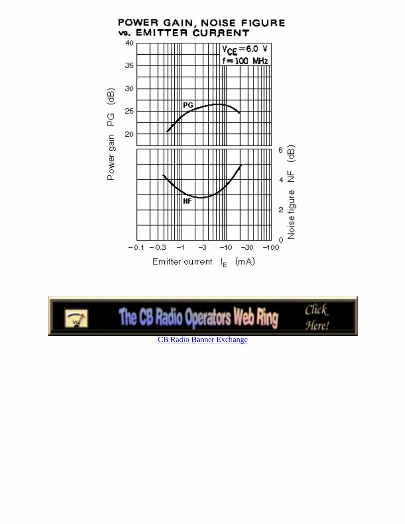
CB Radio Banner Exchange
2SC1342Silicon NPN Transistor
High frequency applications.
The 2SC1342 is a silicon NPN planar epitaxialtransistor in a TO-92 type package. This device issuitable for use as VHF amplifier, Oscillator and Mixerapplications.
ECB
Absolute Maximum Ratings: (TA = +25°C unless otherwise specified)
Collector-Base Voltage, VCBO 30VCollector-Emitter Voltage, VCEO 20VEmitter-Base Voltage, VEBO 4VCollector Current, IC 30mATotal Device Dissipation (TA = +25°C), PD 100mWOperating Junction Temperature, TJ +150°CStorage Temperature Range, Tstg -55° to +150°C
Electrical Characteristics:(TA = +25°C unless otherwise specified)
Parameter Symbol Test Conditions Min Typ Max Unit
Forward Current Transfer Ratio hFE VCE = 6V, IC = 1mA 35 - 200
Current Gain-Bandwidth Product fT VCE = 6V, IC = 1mA 150 320 - MHz
Power Gain PG VCE = 6V, IC = 1mA, f = 100MHz 13 17 - dB
Noise Figure NF VCB = 6V, IC = 1mA, f = 100MHz - 5,5 8,5 dB
CB Radio Banner Exchange

2SC1674Silicon NPN Transistor
High frequency applications.
The 2SC1674 is a silicon NPN planar epitaxialtransistor in a TO-92 type package. This device issuitable for use as FM RF amplifier, Mixer and IFamlifier applications.
ECB
Absolute Maximum Ratings: (TA = +25°C unless otherwise specified)
Collector-Base Voltage, VCBO 30VCollector-Emitter Voltage, VCEO 20VEmitter-Base Voltage, VEBO 4VCollector Current, IC 20mATotal Device Dissipation (TA = +25°C), PD 250mWOperating Junction Temperature, TJ +125°CStorage Temperature Range, Tstg -55° to +125°C
Electrical Characteristics:(TA = +25°C unless otherwise specified)
Parameter Symbol Test Conditions Min Typ Max Unit
Forward Current Transfer Ratio hFE VCE = 6V, IC = 1mA 40 90 180
Current Gain-Bandwidth Product fT IC = 5mA, VCE = 6V, IE 400 600 - MHz
Power Gain PG VCE = 6V, IC = 1mA, f = 100MHz 18 22 - dB
Noise Figure NF IC = 1mA, VCB = 6V, f = 100MHz - 3 5 dB
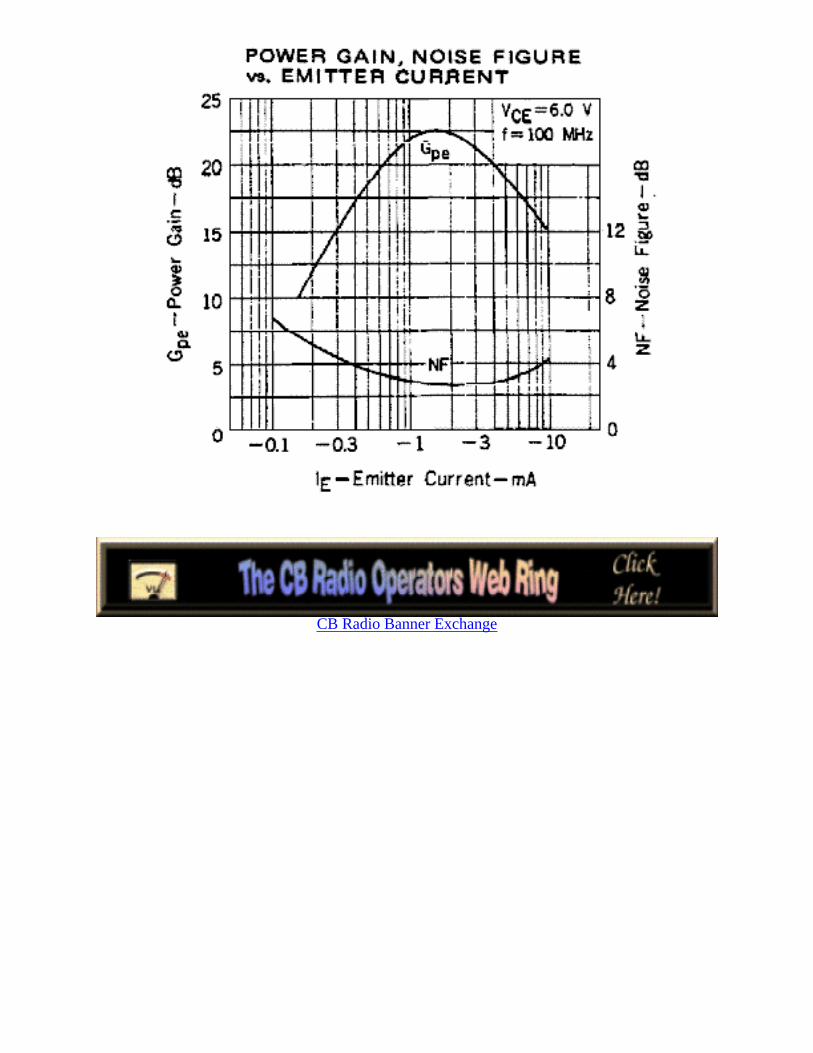
CB Radio Banner Exchange

2SC1906Silicon NPN Transistor
High frequency applications.
The 2SC1906 is a silicon NPN planar epitaxialtransistor in a TO-92 type package. This device issuitable for use as VHF amplifier, Oscillator and Mixerapplications.
ECB
Absolute Maximum Ratings: (TA = +25°C unless otherwise specified)
Collector-Base Voltage, VCBO 30VCollector-Emitter Voltage, VCEO 19VEmitter-Base Voltage, VEBO 2VCollector Current, IC 50mATotal Device Dissipation (TA = +25°C), PD 300mWOperating Junction Temperature, TJ +150°CStorage Temperature Range, Tstg -55° to +150°C
Electrical Characteristics:(TA = +25°C unless otherwise specified)
Parameter Symbol Test Conditions Min Typ Max Unit
Forward Current Transfer Ratio hFE VCE = 10V, IC = 10mA 40 - -
Current Gain-Bandwidth Product fT VCE = 10V, IC = 10mA 600 1000 - MHz
Power Gain PG VCE = 10V, IC = 5mA, f = 200MHz - 18 - dB
CB Radio Banner Exchange

2SC1907Silicon NPN Transistor
High frequency applications.
The 2SC1907 is a silicon NPN planar epitaxialtransistor in a TO-92 type package. This device issuitable for use as UHF Tuner and Oscillatorapplications.
ECB
Absolute Maximum Ratings: (TA = +25°C unless otherwise specified)
Collector-Base Voltage, VCBO 30VCollector-Emitter Voltage, VCEO 19VEmitter-Base Voltage, VEBO 2VCollector Current, IC 50mATotal Device Dissipation (TA = +25°C), PD 300mWOperating Junction Temperature, TJ +150°CStorage Temperature Range, Tstg -55° to +150°C
Electrical Characteristics:(TA = +25°C unless otherwise specified)
Parameter Symbol Test Conditions Min Typ Max Unit
Forward Current Transfer Ratio hFE VCE = 10V, IC = 10mA 40 - -
Current Gain-Bandwidth Product fT VCE = 10V, IC = 10mA 900 1100 - MHz
CB Radio Banner Exchange

2SC1923Silicon NPN Transistor
High frequency applications.
The 2SC1923 is a silicon NPN planar epitaxialtransistor in a TO-92 type package. This device isdesigned for use in FM high frequency amplifier, FM IFamplifier and local oscillator.
ECB
Absolute Maximum Ratings: (TA = +25°C unless otherwise specified)
Collector-Base Voltage, VCBO 40VCollector-Emitter Voltage, VCEO 30VEmitter-Base Voltage, VEBO 4VCollector Current, IC 20mATotal Device Dissipation (TA = +25°C), PD 100mWOperating Junction Temperature, TJ +125°CStorage Temperature Range, Tstg -55° to +125°C
Electrical Characteristics:(TA = +25°C unless otherwise specified)
Parameter Symbol Test Conditions Min Typ Max Unit
Forward Current Transfer Ratio hFE VCE = 6V, IC = 1mA 40 - 200
Gain-Bandwidth Product fT IC = 1mA, VCE = 6V - 550 - MHz
Noise Figure NF VCE = 6V, IC = 1mA, f = 100MHz - 2,5 4 dB
Power Gain PG VCE = 6V, IC = 1mA, f = 100MHz 15 18 - dB
CB Radio Banner Exchange

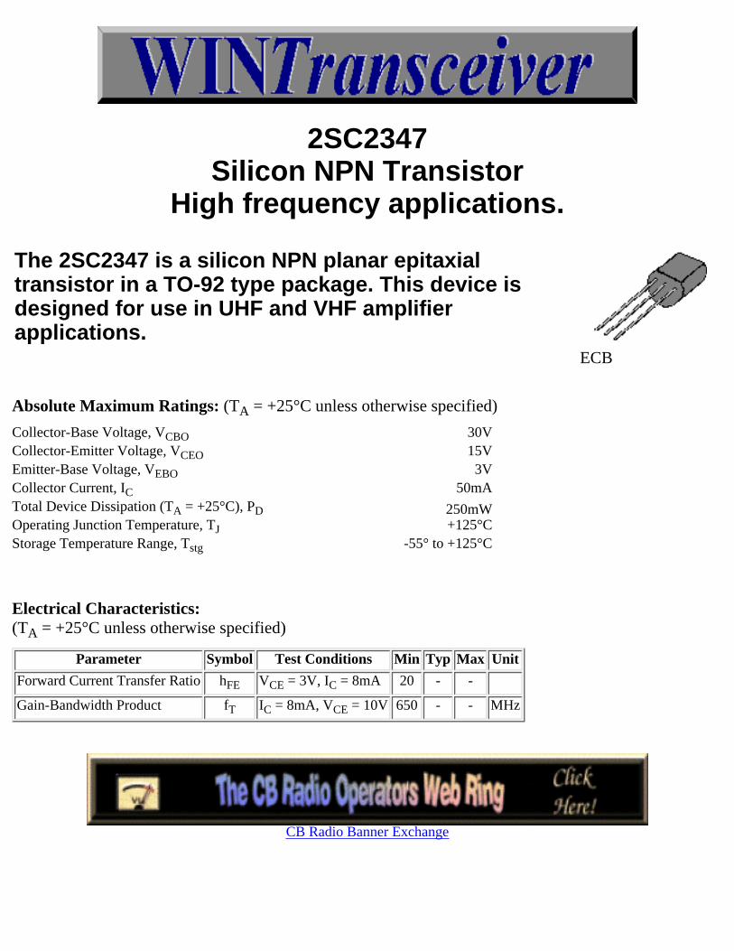
2SC2347Silicon NPN Transistor
High frequency applications.
The 2SC2347 is a silicon NPN planar epitaxialtransistor in a TO-92 type package. This device isdesigned for use in UHF and VHF amplifierapplications.
ECB
Absolute Maximum Ratings: (TA = +25°C unless otherwise specified)
Collector-Base Voltage, VCBO 30VCollector-Emitter Voltage, VCEO 15VEmitter-Base Voltage, VEBO 3VCollector Current, IC 50mATotal Device Dissipation (TA = +25°C), PD 250mWOperating Junction Temperature, TJ +125°CStorage Temperature Range, Tstg -55° to +125°C
Electrical Characteristics:(TA = +25°C unless otherwise specified)
Parameter Symbol Test Conditions Min Typ Max Unit
Forward Current Transfer Ratio hFE VCE = 3V, IC = 8mA 20 - -
Gain-Bandwidth Product fT IC = 8mA, VCE = 10V 650 - - MHz
CB Radio Banner Exchange
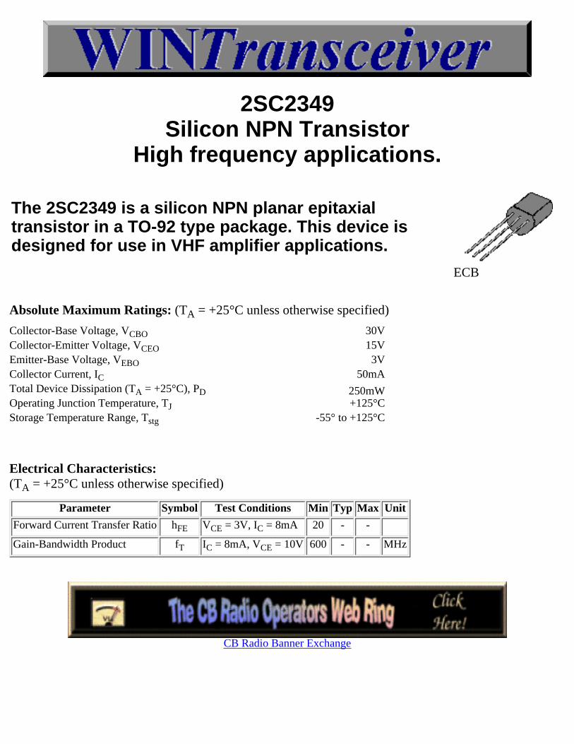
2SC2349Silicon NPN Transistor
High frequency applications.
The 2SC2349 is a silicon NPN planar epitaxialtransistor in a TO-92 type package. This device isdesigned for use in VHF amplifier applications.
ECB
Absolute Maximum Ratings: (TA = +25°C unless otherwise specified)
Collector-Base Voltage, VCBO 30VCollector-Emitter Voltage, VCEO 15VEmitter-Base Voltage, VEBO 3VCollector Current, IC 50mATotal Device Dissipation (TA = +25°C), PD 250mWOperating Junction Temperature, TJ +125°CStorage Temperature Range, Tstg -55° to +125°C
Electrical Characteristics:(TA = +25°C unless otherwise specified)
Parameter Symbol Test Conditions Min Typ Max Unit
Forward Current Transfer Ratio hFE VCE = 3V, IC = 8mA 20 - -
Gain-Bandwidth Product fT IC = 8mA, VCE = 10V 600 - - MHz
CB Radio Banner Exchange

2SC2471Silicon NPN Transistor
High frequency applications.
The 2SC2471 is a silicon NPN planar epitaxialtransistor in a TO-92 type package. This device issuitable for use as UHF Tuner and Oscillatorapplications.
ECB
Absolute Maximum Ratings: (TA = +25°C unless otherwise specified)
Collector-Base Voltage, VCBO 30VCollector-Emitter Voltage, VCEO 30VEmitter-Base Voltage, VEBO 3VCollector Current, IC 50mATotal Device Dissipation (TA = +25°C), PD 310mWOperating Junction Temperature, TJ +150°CStorage Temperature Range, Tstg -55° to +150°C
Electrical Characteristics:(TA = +25°C unless otherwise specified)
Parameter Symbol Test Conditions Min Typ Max Unit
Forward Current Transfer Ratio hFE VCE = 10V, IC = 5mA 20 - -
Current Gain-Bandwidth Product fT VCE = 10V, IC = 5mA 1000 2000 - MHz
CB Radio Banner Exchange
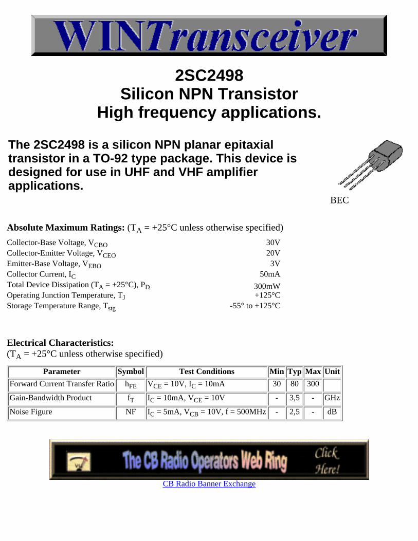
2SC2498Silicon NPN Transistor
High frequency applications.
The 2SC2498 is a silicon NPN planar epitaxialtransistor in a TO-92 type package. This device isdesigned for use in UHF and VHF amplifierapplications.
BEC
Absolute Maximum Ratings: (TA = +25°C unless otherwise specified)
Collector-Base Voltage, VCBO 30VCollector-Emitter Voltage, VCEO 20VEmitter-Base Voltage, VEBO 3VCollector Current, IC 50mATotal Device Dissipation (TA = +25°C), PD 300mWOperating Junction Temperature, TJ +125°CStorage Temperature Range, Tstg -55° to +125°C
Electrical Characteristics:(TA = +25°C unless otherwise specified)
Parameter Symbol Test Conditions Min Typ Max Unit
Forward Current Transfer Ratio hFE VCE = 10V, IC = 10mA 30 80 300
Gain-Bandwidth Product fT IC = 10mA, VCE = 10V - 3,5 - GHz
Noise Figure NF IC = 5mA, VCB = 10V, f = 500MHz - 2,5 - dB
CB Radio Banner Exchange

2SC2512Silicon NPN Transistor
High frequency applications.
The 2SC2512 is a silicon NPN planar epitaxialtransistor in a TO-92 type package. This device issuitable for use as VHF Tuner and Oscillatorapplications.
ECB
Absolute Maximum Ratings: (TA = +25°C unless otherwise specified)
Collector-Base Voltage, VCBO 30VCollector-Emitter Voltage, VCEO 20VEmitter-Base Voltage, VEBO 3VCollector Current, IC 50mATotal Device Dissipation (TA = +25°C), PD 300mWOperating Junction Temperature, TJ +150°CStorage Temperature Range, Tstg -55° to +150°C
Electrical Characteristics:(TA = +25°C unless otherwise specified)
Parameter Symbol Test Conditions Min Typ Max Unit
Forward Current Transfer Ratio hFE VCE = 10V, IC = 10mA 30 - -
Current Gain-Bandwidth Product fT VCE = 10V, IC = 10mA 600 900 - MHz
Power Gain PG VCE = 12V, IC = 2mA, f = 200MHz 16 20 - dB
Noise Figure NF VCB = 12V, IC = 2mA, f = 200MHz - 3,8 5,5 dB
CB Radio Banner Exchange

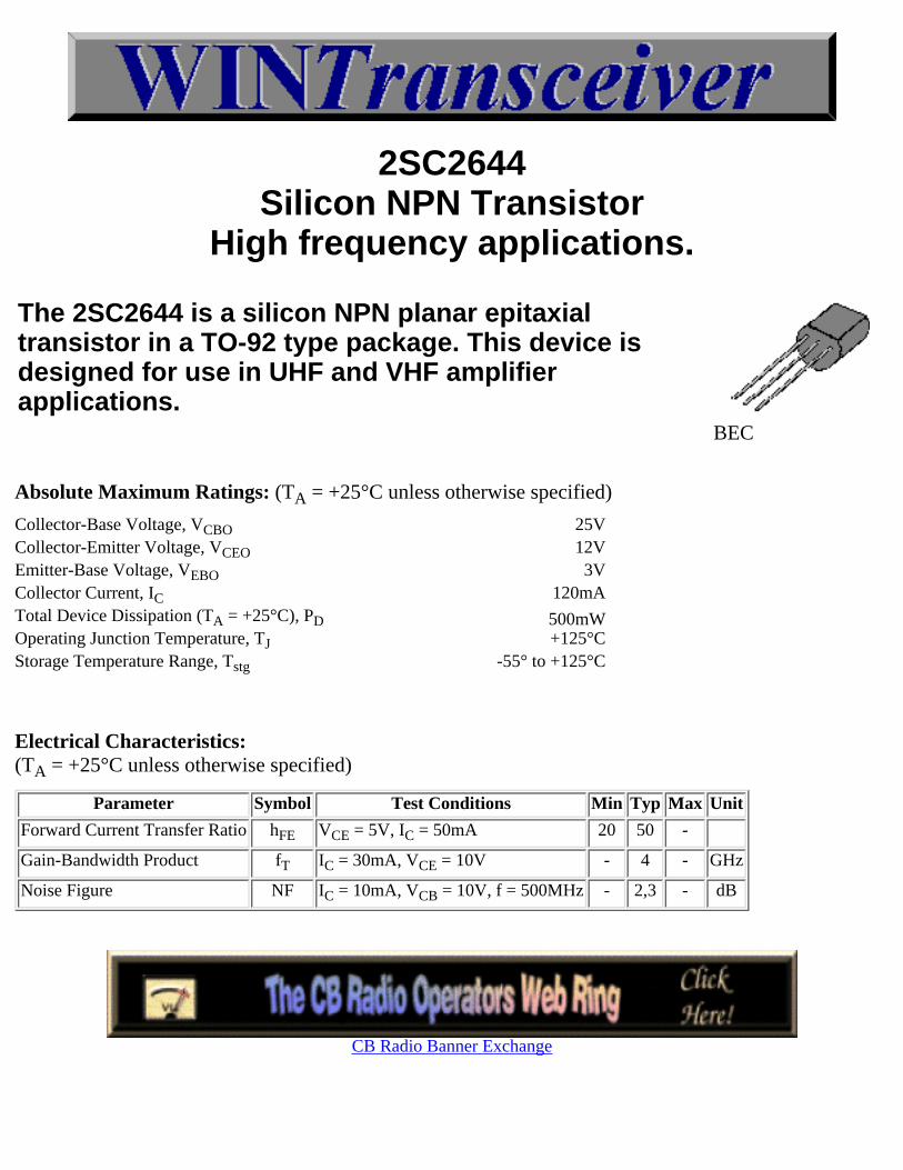
2SC2644Silicon NPN Transistor
High frequency applications.
The 2SC2644 is a silicon NPN planar epitaxialtransistor in a TO-92 type package. This device isdesigned for use in UHF and VHF amplifierapplications.
BEC
Absolute Maximum Ratings: (TA = +25°C unless otherwise specified)
Collector-Base Voltage, VCBO 25VCollector-Emitter Voltage, VCEO 12VEmitter-Base Voltage, VEBO 3VCollector Current, IC 120mATotal Device Dissipation (TA = +25°C), PD 500mWOperating Junction Temperature, TJ +125°CStorage Temperature Range, Tstg -55° to +125°C
Electrical Characteristics:(TA = +25°C unless otherwise specified)
Parameter Symbol Test Conditions Min Typ Max Unit
Forward Current Transfer Ratio hFE VCE = 5V, IC = 50mA 20 50 -
Gain-Bandwidth Product fT IC = 30mA, VCE = 10V - 4 - GHz
Noise Figure NF IC = 10mA, VCB = 10V, f = 500MHz - 2,3 - dB
CB Radio Banner Exchange
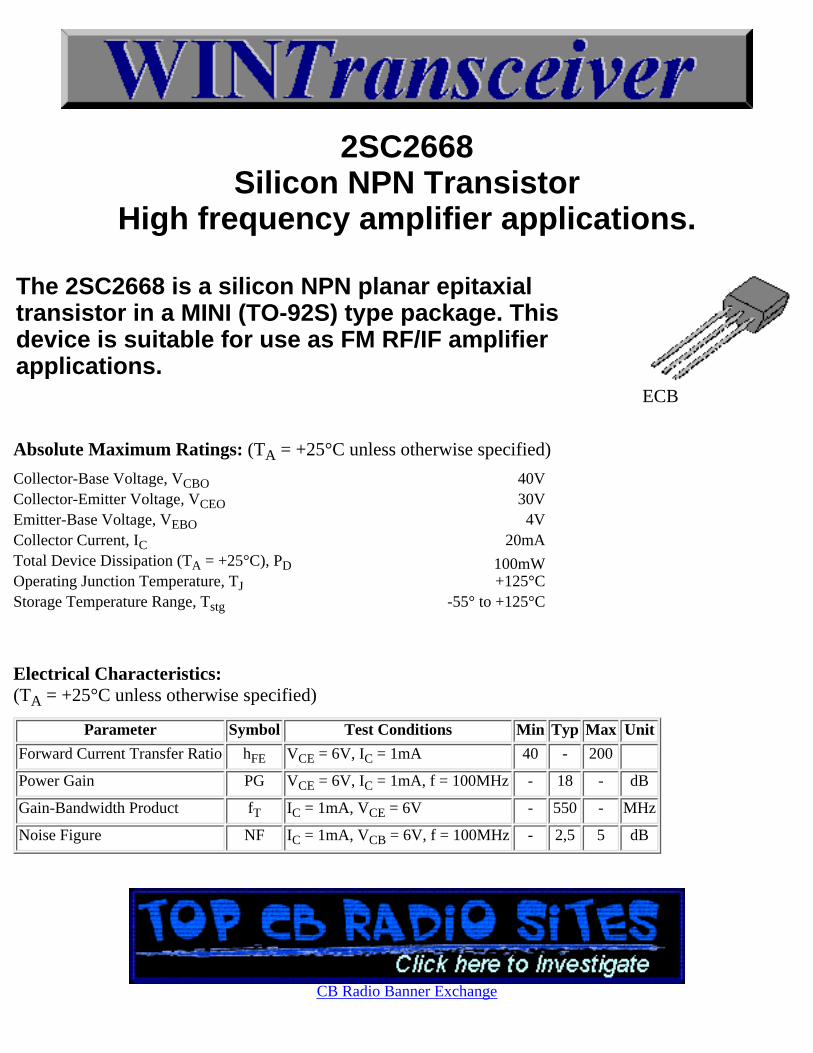
2SC2668Silicon NPN Transistor
High frequency amplifier applications.
The 2SC2668 is a silicon NPN planar epitaxialtransistor in a MINI (TO-92S) type package. Thisdevice is suitable for use as FM RF/IF amplifierapplications.
ECB
Absolute Maximum Ratings: (TA = +25°C unless otherwise specified)
Collector-Base Voltage, VCBO 40VCollector-Emitter Voltage, VCEO 30VEmitter-Base Voltage, VEBO 4VCollector Current, IC 20mATotal Device Dissipation (TA = +25°C), PD 100mWOperating Junction Temperature, TJ +125°CStorage Temperature Range, Tstg -55° to +125°C
Electrical Characteristics:(TA = +25°C unless otherwise specified)
Parameter Symbol Test Conditions Min Typ Max Unit
Forward Current Transfer Ratio hFE VCE = 6V, IC = 1mA 40 - 200
Power Gain PG VCE = 6V, IC = 1mA, f = 100MHz - 18 - dB
Gain-Bandwidth Product fT IC = 1mA, VCE = 6V - 550 - MHz
Noise Figure NF IC = 1mA, VCB = 6V, f = 100MHz - 2,5 5 dB
CB Radio Banner Exchange


2SC2669Silicon NPN Transistor
High frequency applications.
The 2SC2669 is a silicon NPN planar epitaxialtransistor in a TO-92S (MINI) type package. Thisdevice is designed for use in AM converter, AM/FM IFamplifier and local oscillator in AM/FM tuner.
ECB
Absolute Maximum Ratings: (TA = +25°C unless otherwise specified)
Collector-Base Voltage, VCBO 35VCollector-Emitter Voltage, VCEO 30VEmitter-Base Voltage, VEBO 4VCollector Current, IC 50mATotal Device Dissipation (TA = +25°C), PD 200mWOperating Junction Temperature, TJ +125°CStorage Temperature Range, Tstg -55° to +125°C
Electrical Characteristics:(TA = +25°C unless otherwise specified)
Parameter Symbol Test Conditions Min Typ Max Unit
Forward Current Transfer Ratio hFE VCE = 12V, IC = 2mA 40 - 240
Gain-Bandwidth Product fT IC = 1mA, VCE = 10V 100 - - MHz
Power Gain PG VCE = 6V, IC = 1mA, f = 10,7MHz 27 30 33 dB
CB Radio Banner Exchange
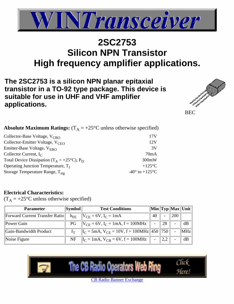
2SC2753Silicon NPN Transistor
High frequency amplifier applications.
The 2SC2753 is a silicon NPN planar epitaxialtransistor in a TO-92 type package. This device issuitable for use in UHF and VHF amplifierapplications.
BEC
Absolute Maximum Ratings: (TA = +25°C unless otherwise specified)
Collector-Base Voltage, VCBO 17VCollector-Emitter Voltage, VCEO 12VEmitter-Base Voltage, VEBO 3VCollector Current, IC 70mATotal Device Dissipation (TA = +25°C), PD 300mWOperating Junction Temperature, TJ +125°CStorage Temperature Range, Tstg -40° to +125°C
Electrical Characteristics:(TA = +25°C unless otherwise specified)
Parameter Symbol Test Conditions Min Typ Max Unit
Forward Current Transfer Ratio hFE VCE = 6V, IC = 1mA 40 - 200
Power Gain PG VCE = 6V, IC = 1mA, f = 100MHz - 28 - dB
Gain-Bandwidth Product fT IC = 5mA, VCE = 10V, f = 100MHz 450 750 - MHz
Noise Figure NF IC = 1mA, VCB = 6V, f = 100MHz - 2,2 - dB
CB Radio Banner Exchange


2SC2786Silicon NPN Transistor
High frequency applications.
The 2SC2786 is a silicon NPN planar epitaxialtransistor in a MINI (TO-92S) type package. Thisdevice is designed for use in FM RF amplifier andlocal oscillator of FM tuner.
ECB
Absolute Maximum Ratings: (TA = +25°C unless otherwise specified)
Collector-Base Voltage, VCBO 30VCollector-Emitter Voltage, VCEO 20VEmitter-Base Voltage, VEBO 4VCollector Current, IC 20mATotal Device Dissipation (TA = +25°C), PD 150mWOperating Junction Temperature, TJ +150°CStorage Temperature Range, Tstg -55° to +125°C
Electrical Characteristics:(TA = +25°C unless otherwise specified)
Parameter Symbol Test Conditions Min Typ Max Unit
Forward Current Transfer Ratio hFE VCE = 6V, IC = 1mA 40 90 180
Current Gain-Bandwidth Product fT IC = 1mA, VCE = 6V, IE 400 600 - MHz
Power Gain PG VCE = 6V, IC = 1mA, f = 100MHz 18 22 - dB
Noise Figure NF IC = 1mA, VCB = 6V, f = 100MHz - 3 5 dB
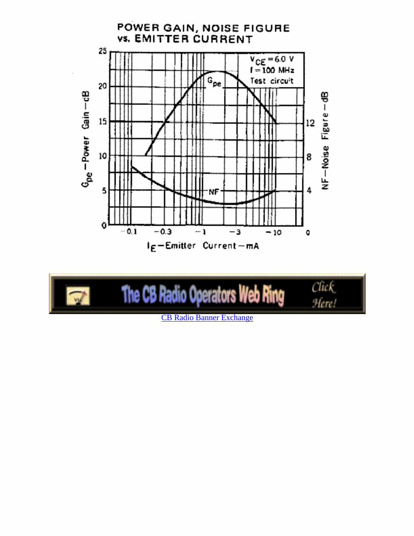
CB Radio Banner Exchange
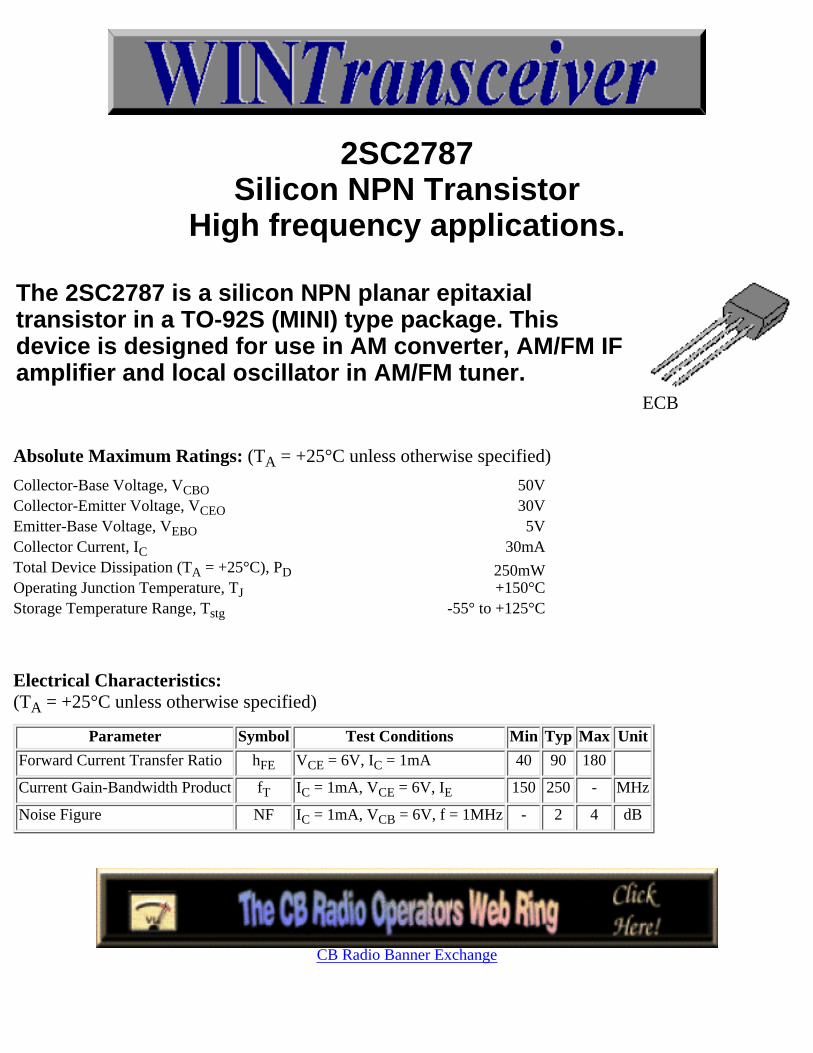
2SC2787Silicon NPN Transistor
High frequency applications.
The 2SC2787 is a silicon NPN planar epitaxialtransistor in a TO-92S (MINI) type package. Thisdevice is designed for use in AM converter, AM/FM IFamplifier and local oscillator in AM/FM tuner.
ECB
Absolute Maximum Ratings: (TA = +25°C unless otherwise specified)
Collector-Base Voltage, VCBO 50VCollector-Emitter Voltage, VCEO 30VEmitter-Base Voltage, VEBO 5VCollector Current, IC 30mATotal Device Dissipation (TA = +25°C), PD 250mWOperating Junction Temperature, TJ +150°CStorage Temperature Range, Tstg -55° to +125°C
Electrical Characteristics:(TA = +25°C unless otherwise specified)
Parameter Symbol Test Conditions Min Typ Max Unit
Forward Current Transfer Ratio hFE VCE = 6V, IC = 1mA 40 90 180
Current Gain-Bandwidth Product fT IC = 1mA, VCE = 6V, IE 150 250 - MHz
Noise Figure NF IC = 1mA, VCB = 6V, f = 1MHz - 2 4 dB
CB Radio Banner Exchange
2SC2814Silicon NPN Transistor
High frequency applications.
The 2SC2814 is a silicon NPN planar epitaxialtransistor in a SOT type package. This device isdesigned for general purpose amplifier applications.
Absolute Maximum Ratings: (TA = +25°C unless otherwise specified)
Collector-Base Voltage, VCBO 30VCollector-Emitter Voltage, VCEO 20VEmitter-Base Voltage, VEBO 5VCollector Current, IC 30mATotal Device Dissipation (TA = +25°C), PD 150mWOperating Junction Temperature, TJ +125°CStorage Temperature Range, Tstg -55° to +125°C
Electrical Characteristics:(TA = +25°C unless otherwise specified)
Parameter Symbol Test Conditions Min Typ Max Unit
Forward Current Transfer Ratio hFE VCE = 6V, IC = 1mA 40 - 270
Gain-Bandwidth Product fT IC = 1mA, VCE = 6V, 200 230 - MHz
Power Gain PG VCE = 6V, IC = 1mA, f = 100MHz - 25 - dB
Noise Figure NF IC = 1mA, VCB = 6V, f = 100MHz - 3 - dB
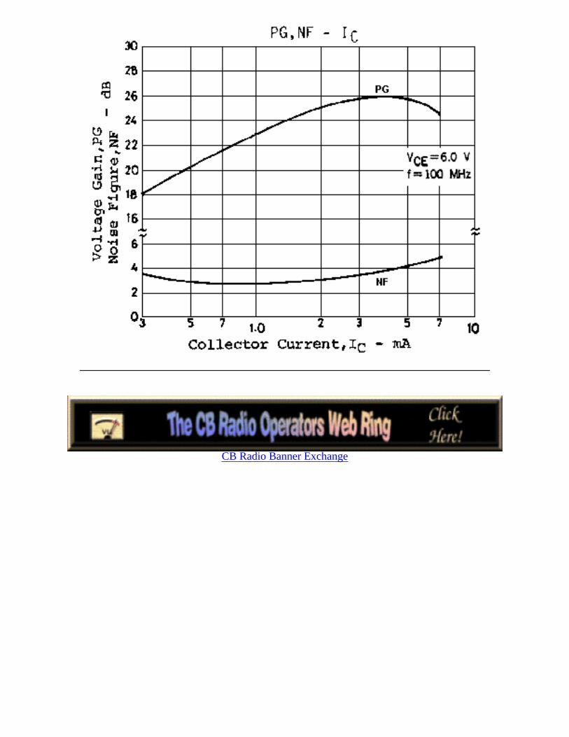
CB Radio Banner Exchange
2SC2839Silicon NPN Transistor
High frequency applications.
The 2SC2839 is a silicon NPN planar epitaxialtransistor in a TO-92S (MINI) type package.
ECB
Absolute Maximum Ratings: (TA = +25°C unless otherwise specified)
Collector-Base Voltage, VCBO 30VCollector-Emitter Voltage, VCEO 20VEmitter-Base Voltage, VEBO 5VCollector Current, IC 30mATotal Device Dissipation (TA = +25°C), PD 150mWOperating Junction Temperature, TJ +125°CStorage Temperature Range, Tstg -55° to +125°C
Electrical Characteristics:(TA = +25°C unless otherwise specified)
Parameter Symbol Test Conditions Min Typ Max Unit
Forward Current Transfer Ratio hFE VCE = 6V, IC = 1mA 60 - 320
Gain-Bandwidth Product fT IC = 1mA, VCE = 6V 200 320 - MHz
Power Gain PG VCE = 6V, IC = 1mA, f = 100MHz - 25 - dB
Noise Figure NF IC = 1mA, VCB = 6V, f = 100MHz - 3 - dB
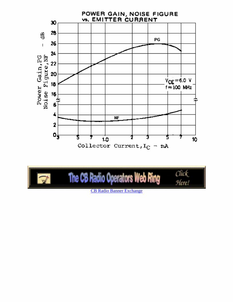
CB Radio Banner Exchange
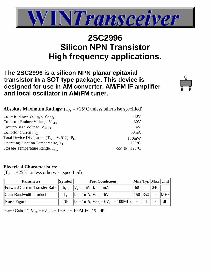
2SC2996Silicon NPN Transistor
High frequency applications.
The 2SC2996 is a silicon NPN planar epitaxialtransistor in a SOT type package. This device isdesigned for use in AM converter, AM/FM IF amplifierand local oscillator in AM/FM tuner.
Absolute Maximum Ratings: (TA = +25°C unless otherwise specified)
Collector-Base Voltage, VCBO 40VCollector-Emitter Voltage, VCEO 30VEmitter-Base Voltage, VEBO 4VCollector Current, IC 50mATotal Device Dissipation (TA = +25°C), PD 150mWOperating Junction Temperature, TJ +125°CStorage Temperature Range, Tstg -55° to +125°C
Electrical Characteristics:(TA = +25°C unless otherwise specified)
Parameter Symbol Test Conditions Min Typ Max Unit
Forward Current Transfer Ratio hFE VCE = 6V, IC = 1mA 60 - 240
Gain-Bandwidth Product fT IC = 1mA, VCE = 6V 150 350 - MHz
Noise Figure NF IC = 1mA, VCB = 6V, f = 100MHz - 4 - dB
Power Gain PG VCE = 6V, IC = 1mA, f = 100MHz - 15 - dB
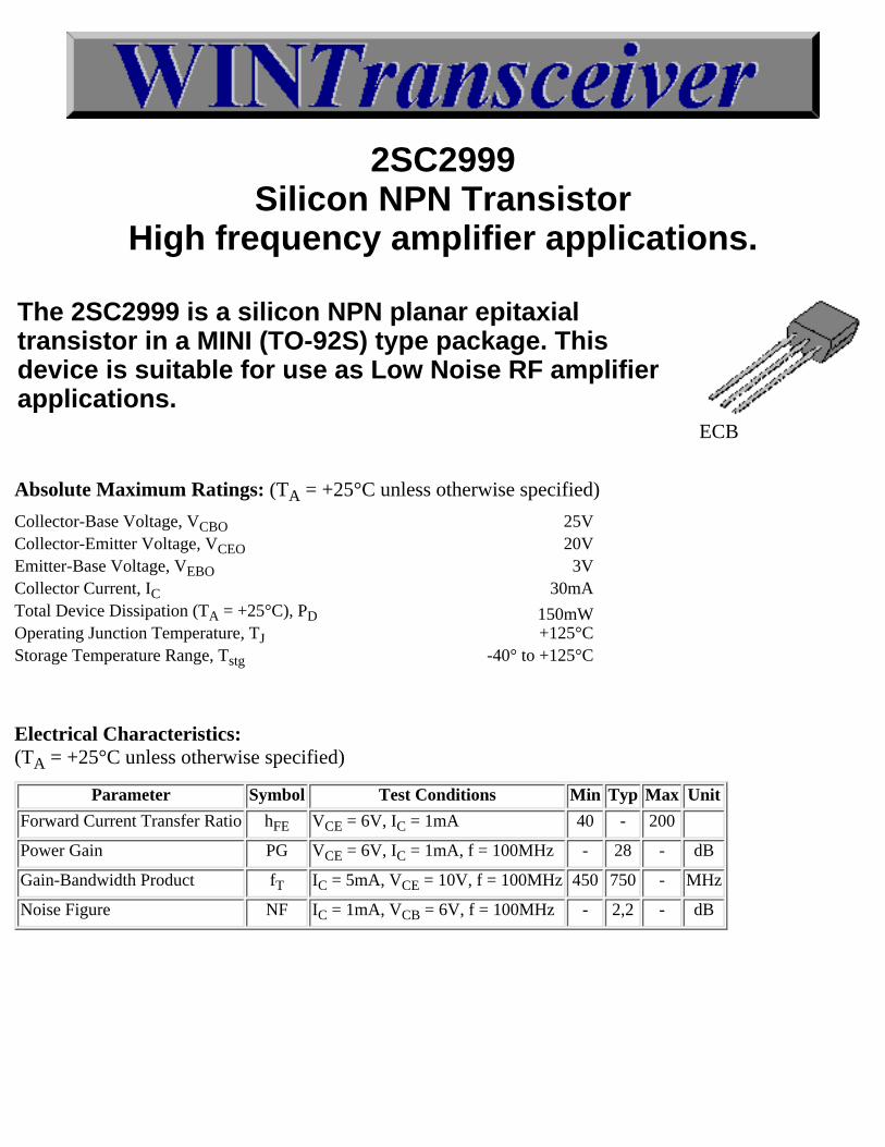
2SC2999Silicon NPN Transistor
High frequency amplifier applications.
The 2SC2999 is a silicon NPN planar epitaxialtransistor in a MINI (TO-92S) type package. Thisdevice is suitable for use as Low Noise RF amplifierapplications.
ECB
Absolute Maximum Ratings: (TA = +25°C unless otherwise specified)
Collector-Base Voltage, VCBO 25VCollector-Emitter Voltage, VCEO 20VEmitter-Base Voltage, VEBO 3VCollector Current, IC 30mATotal Device Dissipation (TA = +25°C), PD 150mWOperating Junction Temperature, TJ +125°CStorage Temperature Range, Tstg -40° to +125°C
Electrical Characteristics:(TA = +25°C unless otherwise specified)
Parameter Symbol Test Conditions Min Typ Max Unit
Forward Current Transfer Ratio hFE VCE = 6V, IC = 1mA 40 - 200
Power Gain PG VCE = 6V, IC = 1mA, f = 100MHz - 28 - dB
Gain-Bandwidth Product fT IC = 5mA, VCE = 10V, f = 100MHz 450 750 - MHz
Noise Figure NF IC = 1mA, VCB = 6V, f = 100MHz - 2,2 - dB

CB Radio Banner Exchange
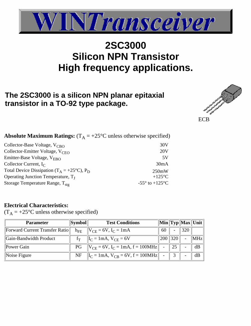
2SC3000Silicon NPN Transistor
High frequency applications.
The 2SC3000 is a silicon NPN planar epitaxialtransistor in a TO-92 type package.
ECB
Absolute Maximum Ratings: (TA = +25°C unless otherwise specified)
Collector-Base Voltage, VCBO 30VCollector-Emitter Voltage, VCEO 20VEmitter-Base Voltage, VEBO 5VCollector Current, IC 30mATotal Device Dissipation (TA = +25°C), PD 250mWOperating Junction Temperature, TJ +125°CStorage Temperature Range, Tstg -55° to +125°C
Electrical Characteristics:(TA = +25°C unless otherwise specified)
Parameter Symbol Test Conditions Min Typ Max Unit
Forward Current Transfer Ratio hFE VCE = 6V, IC = 1mA 60 - 320
Gain-Bandwidth Product fT IC = 1mA, VCE = 6V 200 320 - MHz
Power Gain PG VCE = 6V, IC = 1mA, f = 100MHz - 25 - dB
Noise Figure NF IC = 1mA, VCB = 6V, f = 100MHz - 3 - dB
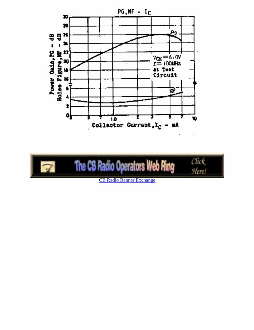
CB Radio Banner Exchange
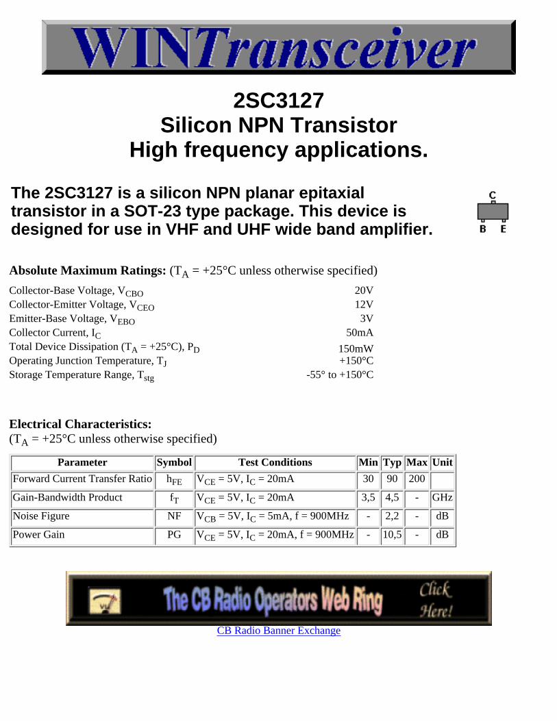
2SC3127Silicon NPN Transistor
High frequency applications.
The 2SC3127 is a silicon NPN planar epitaxialtransistor in a SOT-23 type package. This device isdesigned for use in VHF and UHF wide band amplifier.
Absolute Maximum Ratings: (TA = +25°C unless otherwise specified)
Collector-Base Voltage, VCBO 20VCollector-Emitter Voltage, VCEO 12VEmitter-Base Voltage, VEBO 3VCollector Current, IC 50mATotal Device Dissipation (TA = +25°C), PD 150mWOperating Junction Temperature, TJ +150°CStorage Temperature Range, Tstg -55° to +150°C
Electrical Characteristics:(TA = +25°C unless otherwise specified)
Parameter Symbol Test Conditions Min Typ Max Unit
Forward Current Transfer Ratio hFE VCE = 5V, IC = 20mA 30 90 200
Gain-Bandwidth Product fT VCE = 5V, IC = 20mA 3,5 4,5 - GHz
Noise Figure NF VCB = 5V, IC = 5mA, f = 900MHz - 2,2 - dB
Power Gain PG VCE = 5V, IC = 20mA, f = 900MHz - 10,5 - dB
CB Radio Banner Exchange
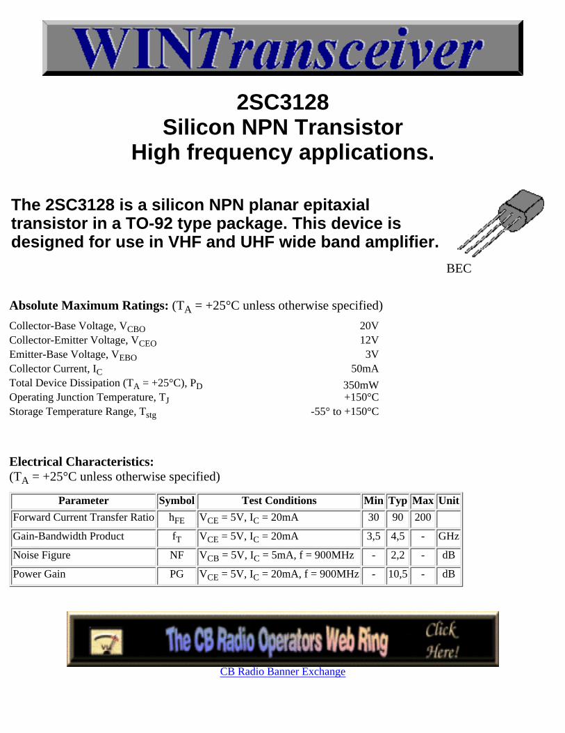
2SC3128Silicon NPN Transistor
High frequency applications.
The 2SC3128 is a silicon NPN planar epitaxialtransistor in a TO-92 type package. This device isdesigned for use in VHF and UHF wide band amplifier.
BEC
Absolute Maximum Ratings: (TA = +25°C unless otherwise specified)
Collector-Base Voltage, VCBO 20VCollector-Emitter Voltage, VCEO 12VEmitter-Base Voltage, VEBO 3VCollector Current, IC 50mATotal Device Dissipation (TA = +25°C), PD 350mWOperating Junction Temperature, TJ +150°CStorage Temperature Range, Tstg -55° to +150°C
Electrical Characteristics:(TA = +25°C unless otherwise specified)
Parameter Symbol Test Conditions Min Typ Max Unit
Forward Current Transfer Ratio hFE VCE = 5V, IC = 20mA 30 90 200
Gain-Bandwidth Product fT VCE = 5V, IC = 20mA 3,5 4,5 - GHz
Noise Figure NF VCB = 5V, IC = 5mA, f = 900MHz - 2,2 - dB
Power Gain PG VCE = 5V, IC = 20mA, f = 900MHz - 10,5 - dB
CB Radio Banner Exchange
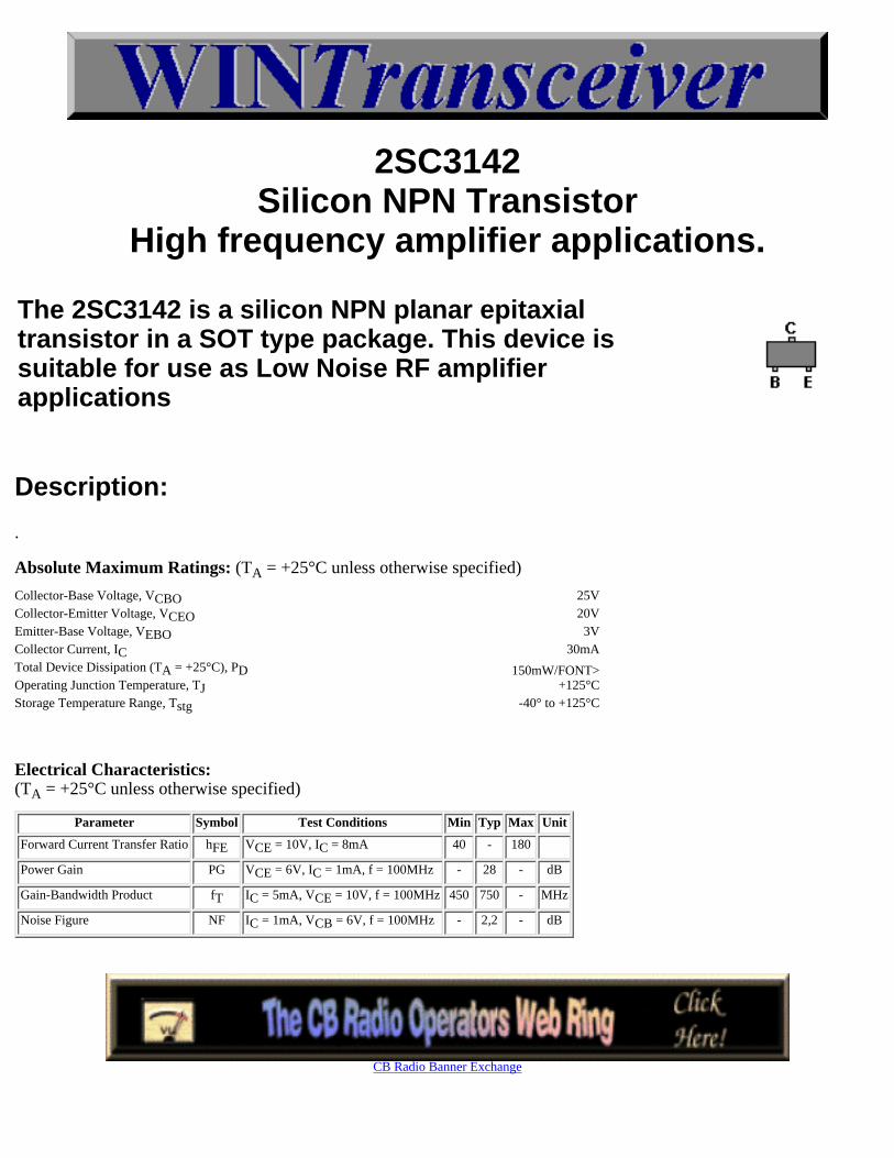
2SC3142Silicon NPN Transistor
High frequency amplifier applications.
The 2SC3142 is a silicon NPN planar epitaxialtransistor in a SOT type package. This device issuitable for use as Low Noise RF amplifierapplications
Description:
.
Absolute Maximum Ratings: (TA = +25°C unless otherwise specified)
Collector-Base Voltage, VCBO 25VCollector-Emitter Voltage, VCEO 20VEmitter-Base Voltage, VEBO 3VCollector Current, IC 30mATotal Device Dissipation (TA = +25°C), PD 150mW/FONT>Operating Junction Temperature, TJ +125°CStorage Temperature Range, Tstg -40° to +125°C
Electrical Characteristics:(TA = +25°C unless otherwise specified)
Parameter Symbol Test Conditions Min Typ Max Unit
Forward Current Transfer Ratio hFE VCE = 10V, IC = 8mA 40 - 180
Power Gain PG VCE = 6V, IC = 1mA, f = 100MHz - 28 - dB
Gain-Bandwidth Product fT IC = 5mA, VCE = 10V, f = 100MHz 450 750 - MHz
Noise Figure NF IC = 1mA, VCB = 6V, f = 100MHz - 2,2 - dB
CB Radio Banner Exchange
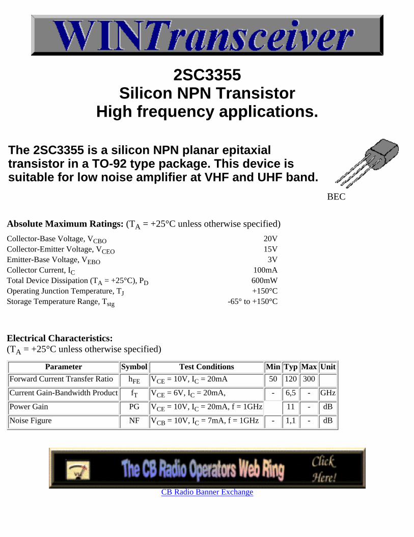
2SC3355Silicon NPN Transistor
High frequency applications.
The 2SC3355 is a silicon NPN planar epitaxialtransistor in a TO-92 type package. This device issuitable for low noise amplifier at VHF and UHF band.
BEC
Absolute Maximum Ratings: (TA = +25°C unless otherwise specified)
Collector-Base Voltage, VCBO 20VCollector-Emitter Voltage, VCEO 15VEmitter-Base Voltage, VEBO 3VCollector Current, IC 100mATotal Device Dissipation (TA = +25°C), PD 600mWOperating Junction Temperature, TJ +150°CStorage Temperature Range, Tstg -65° to +150°C
Electrical Characteristics:(TA = +25°C unless otherwise specified)
Parameter Symbol Test Conditions Min Typ Max Unit
Forward Current Transfer Ratio hFE VCE = 10V, IC = 20mA 50 120 300
Current Gain-Bandwidth Product fT VCE = 6V, IC = 20mA, - 6,5 - GHz
Power Gain PG VCE = 10V, IC = 20mA, f = 1GHz 11 - dB
Noise Figure NF VCB = 10V, IC = 7mA, f = 1GHz - 1,1 - dB
CB Radio Banner Exchange
2SC3356NPN SILICON EPITAXIAL TRANSISTORMICROWAVE LOW NOISE AMPLIFIER
DESCRIPTIONThe 2SC3356 is an NPN silicon epitaxial transistor designed for low noiseamplifier at VHF, UHF and CATV band. It has dynamic range and good currentcharacteristic.FEATURES• Low Noise and High GainNF = 1.1 dB TYP., Ga = 11 dB TYP. @VCE = 10 V, IC = 7 mA, f = 1.0 GHz• High Power GainMAG = 13 dB TYP. @VCE = 10 V, IC = 20 mA, f = 1.0 GHz
Absolute Maximum Ratings: (TA = +25°C unless otherwise specified)
Collector-Base Voltage, VCBO 20VCollector-Emitter Voltage, VCEO 12VEmitter-Base Voltage, VEBO 3VCollector Current, IC 100mATotal Device Dissipation (TA = +25°C), PD 200mWOperating Junction Temperature, TJ +150°CStorage Temperature Range, Tstg -65° to +150°C
Electrical Characteristics:(TA = +25°C unless otherwise specified)
Parameter Symbol Test Conditions Min Typ Max Unit
Forward Current Transfer Ratio hFE VCE =10V, IC = 20mA 50 120 300
Gain-Bandwidth Product fT IC = 20mA, VCE = 10V, - 7 - GHz
Noise Figure NF IC = 7mA, VCB = 10V, f = 1GHz - 1,1 2 dB
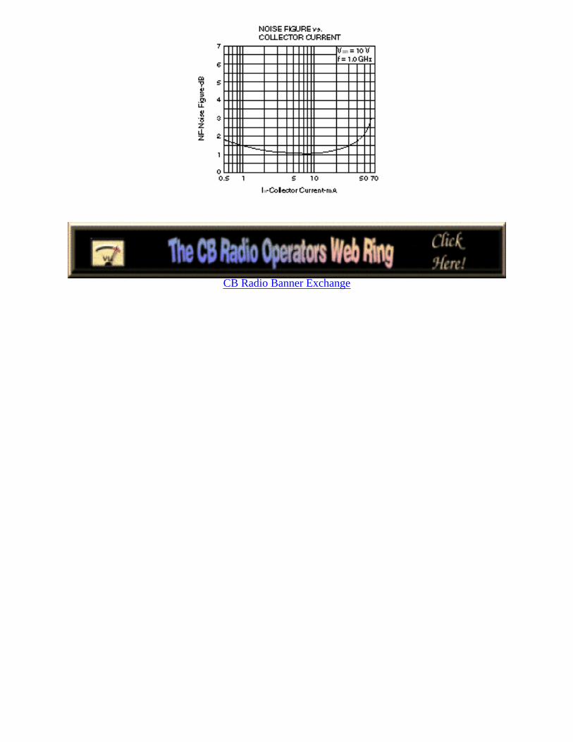
CB Radio Banner Exchange
2SC3510Silicon NPN Transistor
High frequency applications.
The 2SC3510 is a silicon NPN planar epitaxialtransistor in a TO-92 type package. This device isdesigned for use in VHF and UHF wide band amplifier.
BEC
Absolute Maximum Ratings: (TA = +25°C unless otherwise specified)
Collector-Base Voltage, VCBO 20VCollector-Emitter Voltage, VCEO 12VEmitter-Base Voltage, VEBO 3VCollector Current, IC 50mATotal Device Dissipation (TA = +25°C), PD 600mWOperating Junction Temperature, TJ +150°CStorage Temperature Range, Tstg -55° to +150°C
Electrical Characteristics:(TA = +25°C unless otherwise specified)
Parameter Symbol Test Conditions Min Typ Max Unit
Forward Current Transfer Ratio hFE VCE = 5V, IC = 20mA 30 90 200
Gain-Bandwidth Product fT VCE = 5V, IC = 20mA 3,5 4,5 - GHz
Noise Figure NF VCB = 5V, IC = 5mA, f = 900MHz - 2,2 - dB
Power Gain PG VCE = 5V, IC = 20mA, f = 900MHz - 10,5 - dB
CB Radio Banner Exchange

2SC3512Silicon NPN Transistor
High frequency applications.
The 2SC3512 is a silicon NPN planar epitaxialtransistor in a TO-92 type package. This device isdesigned for use in VHF and UHF wide band amplifier.
BEC
Absolute Maximum Ratings: (TA = +25°C unless otherwise specified)
Collector-Base Voltage, VCBO 15VCollector-Emitter Voltage, VCEO 11VEmitter-Base Voltage, VEBO 2VCollector Current, IC 50mATotal Device Dissipation (TA = +25°C), PD 600mWOperating Junction Temperature, TJ +150°CStorage Temperature Range, Tstg -55° to +150°C
Electrical Characteristics:(TA = +25°C unless otherwise specified)
Parameter Symbol Test Conditions Min Typ Max Unit
Forward Current Transfer Ratio hFE VCE = 5V, IC = 20mA 50 120 250
Gain-Bandwidth Product fT VCE = 5V, IC = 20mA - 6 - GHz
Noise Figure NF VCB = 5V, IC = 5mA, f = 900MHz - 1,6 - dB
Power Gain PG VCE = 5V, IC = 20mA, f = 900MHz - 10,5 - dB
CB Radio Banner Exchange

2SC3582Silicon NPN Transistor
High frequency applications.
The 2SC3582 is a silicon NPN planar epitaxialtransistor in a TO-92 type package. This device issuitable for low noise amplifier at VHF and UHF band.
BEC
Absolute Maximum Ratings: (TA = +25°C unless otherwise specified)
Collector-Base Voltage, VCBO 20VCollector-Emitter Voltage, VCEO 10VEmitter-Base Voltage, VEBO 1,5VCollector Current, IC 65mATotal Device Dissipation (TA = +25°C), PD 600mWOperating Junction Temperature, TJ +150°CStorage Temperature Range, Tstg -65° to +150°C
Electrical Characteristics:(TA = +25°C unless otherwise specified)
Parameter Symbol Test Conditions Min Typ Max Unit
Forward Current Transfer Ratio hFE VCE = 8V, IC = 20mA 50 100 250
Current Gain-Bandwidth Product fT VCE = 8V, IC = 20mA, - 8 - GHz
Power Gain PG f = 1GHz - 12 - dB
Noise Figure NF VCB = 8V, IC = 7mA, f = 1GHz - 1,2 2,5 dB
CB Radio Banner Exchange
2SC3605Silicon NPN Transistor
High frequency amplifier applications.
The 2SC3605 is a silicon NPN planar epitaxialtransistor in a TO-92 type package. This device issuitable for use in UHF and VHF amplifierapplications.
BEC
Absolute Maximum Ratings: (TA = +25°C unless otherwise specified)
Collector-Base Voltage, VCBO 20VCollector-Emitter Voltage, VCEO 12VEmitter-Base Voltage, VEBO 3VCollector Current, IC 80mATotal Device Dissipation (TA = +25°C), PD 600mWOperating Junction Temperature, TJ +150°CStorage Temperature Range, Tstg -40° to +150°C
Electrical Characteristics:(TA = +25°C unless otherwise specified)
Parameter Symbol Test Conditions Min Typ Max Unit
Forward Current Transfer Ratio hFE VCE = 10V, IC = 20mA 30 - 250
Gain-Bandwidth Product fT IC = 20mA, VCE = 10V 5 6,5 - GHz
Noise Figure NF IC = 5mA, VCB = 10V, f = 1GHz - 1,1 - dB
CB Radio Banner Exchange
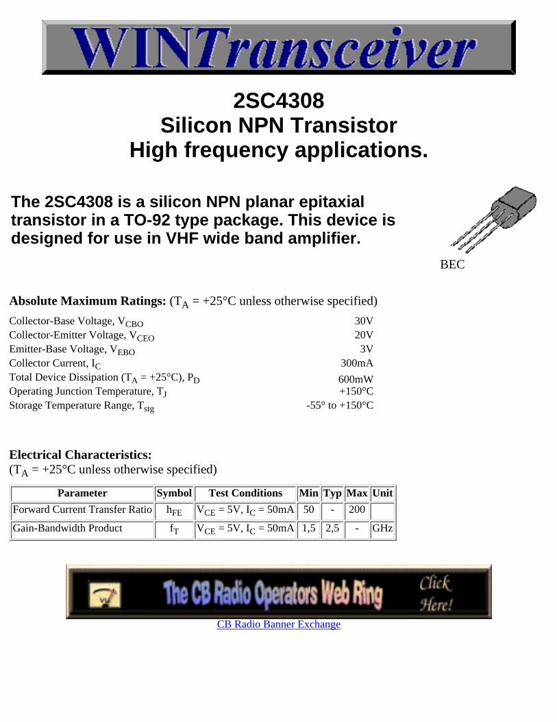
2SC4308Silicon NPN Transistor
High frequency applications.
The 2SC4308 is a silicon NPN planar epitaxialtransistor in a TO-92 type package. This device isdesigned for use in VHF wide band amplifier.
BEC
Absolute Maximum Ratings: (TA = +25°C unless otherwise specified)
Collector-Base Voltage, VCBO 30VCollector-Emitter Voltage, VCEO 20VEmitter-Base Voltage, VEBO 3VCollector Current, IC 300mATotal Device Dissipation (TA = +25°C), PD 600mWOperating Junction Temperature, TJ +150°CStorage Temperature Range, Tstg -55° to +150°C
Electrical Characteristics:(TA = +25°C unless otherwise specified)
Parameter Symbol Test Conditions Min Typ Max Unit
Forward Current Transfer Ratio hFE VCE = 5V, IC = 50mA 50 - 200
Gain-Bandwidth Product fT VCE = 5V, IC = 50mA 1,5 2,5 - GHz
CB Radio Banner Exchange
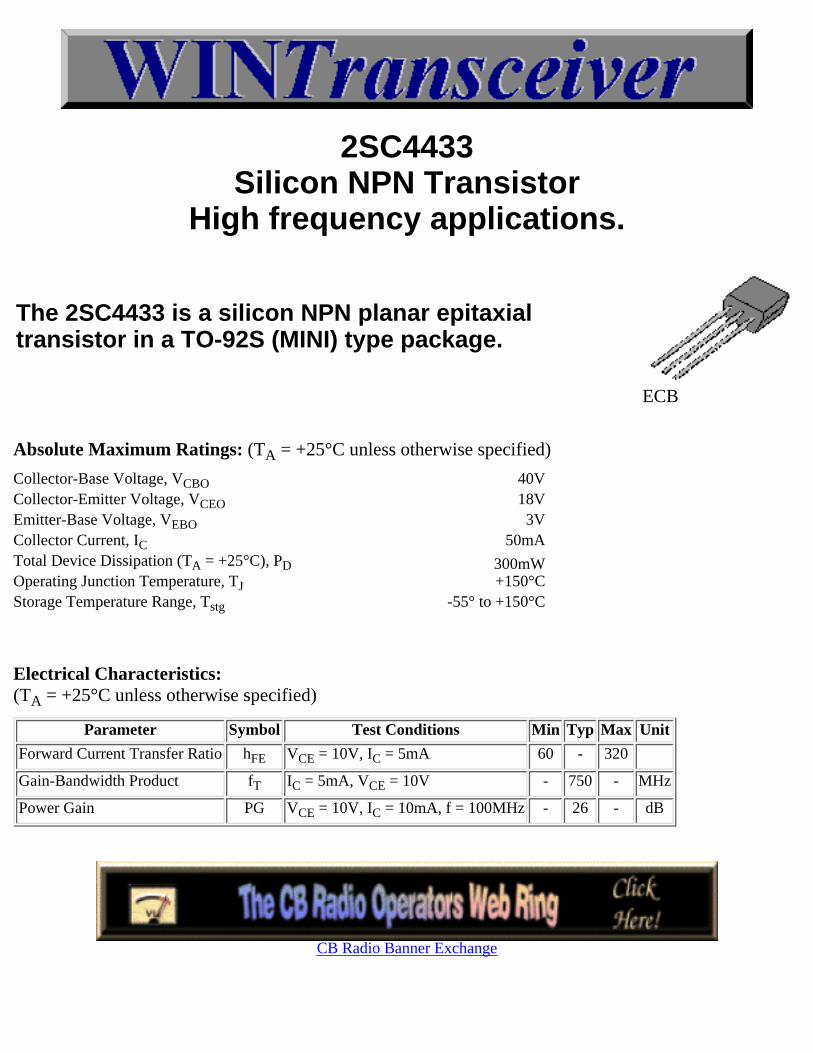
2SC4433Silicon NPN Transistor
High frequency applications.
The 2SC4433 is a silicon NPN planar epitaxialtransistor in a TO-92S (MINI) type package.
ECB
Absolute Maximum Ratings: (TA = +25°C unless otherwise specified)
Collector-Base Voltage, VCBO 40VCollector-Emitter Voltage, VCEO 18VEmitter-Base Voltage, VEBO 3VCollector Current, IC 50mATotal Device Dissipation (TA = +25°C), PD 300mWOperating Junction Temperature, TJ +150°CStorage Temperature Range, Tstg -55° to +150°C
Electrical Characteristics:(TA = +25°C unless otherwise specified)
Parameter Symbol Test Conditions Min Typ Max Unit
Forward Current Transfer Ratio hFE VCE = 10V, IC = 5mA 60 - 320
Gain-Bandwidth Product fT IC = 5mA, VCE = 10V - 750 - MHz
Power Gain PG VCE = 10V, IC = 10mA, f = 100MHz - 26 - dB
CB Radio Banner Exchange

KTC3194Silicon NPN Transistor
High frequency amplifier applications.
The KTC3194 is a silicon NPN planar epitaxialtransistor in a TO-92 type package. This device issuitable for use as Low Noise RF amplifierapplications.
ECB
Absolute Maximum Ratings: (TA = +25°C unless otherwise specified)
Collector-Base Voltage, VCBO 40VCollector-Emitter Voltage, VCEO 30VEmitter-Base Voltage, VEBO 4VCollector Current, IC 20mATotal Device Dissipation (TA = +25°C), PD 625mWOperating Junction Temperature, TJ +150°CStorage Temperature Range, Tstg -50° to +150°C
Electrical Characteristics:(TA = +25°C unless otherwise specified)
Parameter Symbol Test Conditions Min Typ Max Unit
Forward Current Transfer Ratio hFE VCE = 6V, IC = 1mA 40 - 200
Power Gain PG VCE = 6V, IC = 1mA, f = 100MHz 15 18 - dB
Gain-Bandwidth Product fT IC = 1mA, VCE = 6V, f = 100MHz - 550 - MHz
Noise Figure NF IC = 1mA, VCB = 6V, f = 100MHz - 2,5 5 dB
CB Radio Banner Exchange

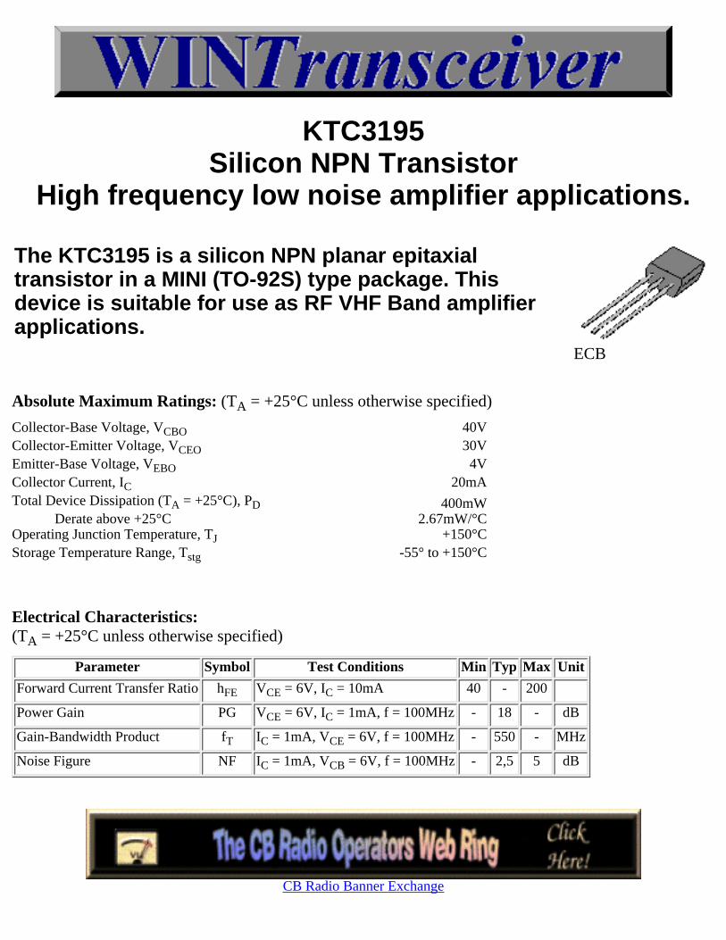
KTC3195Silicon NPN Transistor
High frequency low noise amplifier applications.
The KTC3195 is a silicon NPN planar epitaxialtransistor in a MINI (TO-92S) type package. Thisdevice is suitable for use as RF VHF Band amplifierapplications.
ECB
Absolute Maximum Ratings: (TA = +25°C unless otherwise specified)
Collector-Base Voltage, VCBO 40VCollector-Emitter Voltage, VCEO 30VEmitter-Base Voltage, VEBO 4VCollector Current, IC 20mATotal Device Dissipation (TA = +25°C), PD Derate above +25°C
400mW2.67mW/°C
Operating Junction Temperature, TJ +150°CStorage Temperature Range, Tstg -55° to +150°C
Electrical Characteristics:(TA = +25°C unless otherwise specified)
Parameter Symbol Test Conditions Min Typ Max Unit
Forward Current Transfer Ratio hFE VCE = 6V, IC = 10mA 40 - 200
Power Gain PG VCE = 6V, IC = 1mA, f = 100MHz - 18 - dB
Gain-Bandwidth Product fT IC = 1mA, VCE = 6V, f = 100MHz - 550 - MHz
Noise Figure NF IC = 1mA, VCB = 6V, f = 100MHz - 2,5 5 dB
CB Radio Banner Exchange

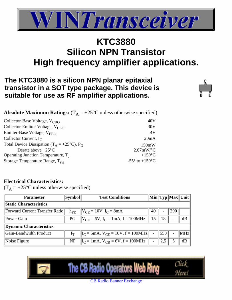
KTC3880Silicon NPN Transistor
High frequency amplifier applications.
The KTC3880 is a silicon NPN planar epitaxialtransistor in a SOT type package. This device issuitable for use as RF amplifier applications.
Absolute Maximum Ratings: (TA = +25°C unless otherwise specified)
Collector-Base Voltage, VCBO 40VCollector-Emitter Voltage, VCEO 30VEmitter-Base Voltage, VEBO 4VCollector Current, IC 20mATotal Device Dissipation (TA = +25°C), PD Derate above +25°C
150mW2.67mW/°C
Operating Junction Temperature, TJ +150°CStorage Temperature Range, Tstg -55° to +150°C
Electrical Characteristics:(TA = +25°C unless otherwise specified)
Parameter Symbol Test Conditions Min Typ Max Unit
Static Characteristics
Forward Current Transfer Ratio hFE VCE = 10V, IC = 8mA 40 - 200
Power Gain PG VCE = 6V, IC = 1mA, f = 100MHz 15 18 - dB
Dynamic Characteristics
Gain-Bandwidth Product fT IC = 5mA, VCE = 10V, f = 100MHz - 550 - MHz
Noise Figure NF IC = 1mA, VCB = 6V, f = 100MHz - 2,5 5 dB
CB Radio Banner Exchange

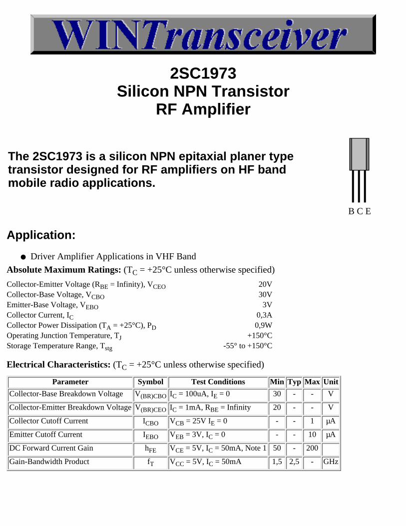
2SC1973Silicon NPN Transistor
RF Amplifier
The 2SC1973 is a silicon NPN epitaxial planer typetransistor designed for RF amplifiers on HF bandmobile radio applications.
B C E
Application:
Driver Amplifier Applications in VHF Band●
Absolute Maximum Ratings: (TC = +25°C unless otherwise specified)
Collector-Emitter Voltage (RBE = Infinity), VCEO 20VCollector-Base Voltage, VCBO 30VEmitter-Base Voltage, VEBO 3VCollector Current, IC 0,3ACollector Power Dissipation (TA = +25°C), PD 0,9WOperating Junction Temperature, TJ +150°CStorage Temperature Range, Tstg -55° to +150°C
Electrical Characteristics: (TC = +25°C unless otherwise specified)
Parameter Symbol Test Conditions Min Typ Max Unit
Collector-Base Breakdown Voltage V(BR)CBO IC = 100uA, IE = 0 30 - - V
Collector-Emitter Breakdown Voltage V(BR)CEO IC = 1mA, RBE = Infinity 20 - - V
Collector Cutoff Current ICBO VCB = 25V IE = 0 - - 1 µA
Emitter Cutoff Current IEBO VEB = 3V, IC = 0 - - 10 µA
DC Forward Current Gain hFE VCE = 5V, IC = 50mA, Note 1 50 - 200
Gain-Bandwidth Product fT VCC = 5V, IC = 50mA 1,5 2,5 - GHz

CB Radio Banner Exchange
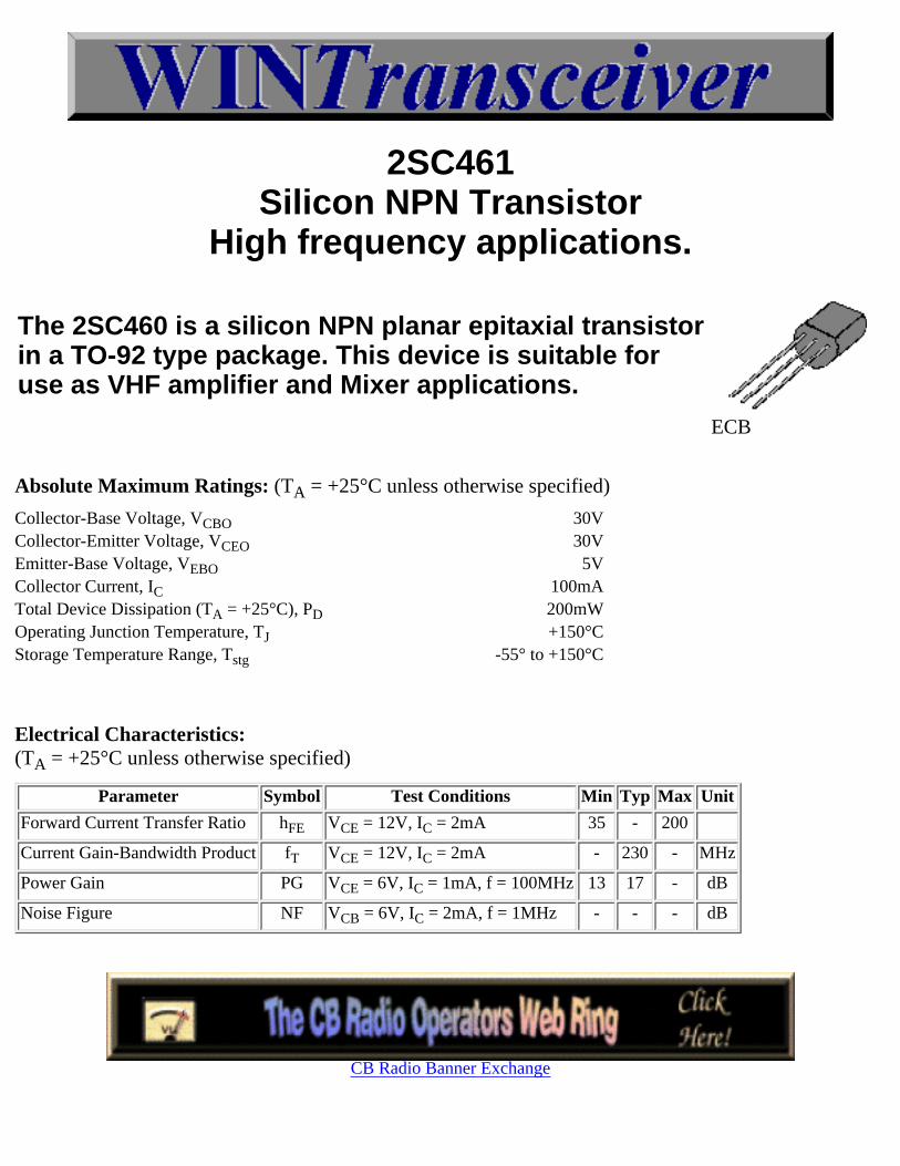
2SC461Silicon NPN Transistor
High frequency applications.
The 2SC460 is a silicon NPN planar epitaxial transistorin a TO-92 type package. This device is suitable foruse as VHF amplifier and Mixer applications.
ECB
Absolute Maximum Ratings: (TA = +25°C unless otherwise specified)
Collector-Base Voltage, VCBO 30VCollector-Emitter Voltage, VCEO 30VEmitter-Base Voltage, VEBO 5VCollector Current, IC 100mATotal Device Dissipation (TA = +25°C), PD 200mWOperating Junction Temperature, TJ +150°CStorage Temperature Range, Tstg -55° to +150°C
Electrical Characteristics:(TA = +25°C unless otherwise specified)
Parameter Symbol Test Conditions Min Typ Max Unit
Forward Current Transfer Ratio hFE VCE = 12V, IC = 2mA 35 - 200
Current Gain-Bandwidth Product fT VCE = 12V, IC = 2mA - 230 - MHz
Power Gain PG VCE = 6V, IC = 1mA, f = 100MHz 13 17 - dB
Noise Figure NF VCB = 6V, IC = 2mA, f = 1MHz - - - dB
CB Radio Banner Exchange
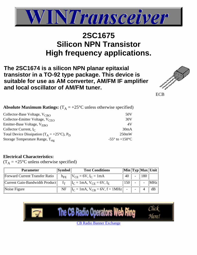
2SC1675Silicon NPN Transistor
High frequency applications.
The 2SC1674 is a silicon NPN planar epitaxialtransistor in a TO-92 type package. This device issuitable for use as AM converter, AM/FM IF amplifierand local oscillator of AM/FM tuner.
ECB
Absolute Maximum Ratings: (TA = +25°C unless otherwise specified)
Collector-Base Voltage, VCBO 50VCollector-Emitter Voltage, VCEO 30VEmitter-Base Voltage, VEBO 4VCollector Current, IC 30mATotal Device Dissipation (TA = +25°C), PD 250mWStorage Temperature Range, Tstg -55° to +150°C
Electrical Characteristics:(TA = +25°C unless otherwise specified)
Parameter Symbol Test Conditions Min Typ Max Unit
Forward Current Transfer Ratio hFE VCE = 6V, IC = 1mA 40 - 180
Current Gain-Bandwidth Product fT IC = 1mA, VCE = 6V, IE 150 - - MHz
Noise Figure NF IC = 1mA, VCB = 6V, f = 1MHz - - 4 dB
CB Radio Banner Exchange