Embed Size (px)
Citation preview
Comparative study of ALD SiO2 thin films for opticalapplicationsPfeiffer, Kristin; Shestaeva, Svetlana; Bingel, Astrid; Munzert, Peter; Ghazaryan, Lilit; vanHelvoirt, C.A.A.; Kessels, W.M.M.; Sanli, Umut T.; Grevent, Corinne; Schütz, G.; Putkonen,M.; Buchanan, Iain; Jensen, Lars; Ristau, Detlev; Tünnermann, Andreas; Szeghalmi, AdrianaPublished in:Optical Materials Express
DOI:10.1364/OME.6.000660
Published: 01/02/2016
Document VersionPublisher’s PDF, also known as Version of Record (includes final page, issue and volume numbers)
Please check the document version of this publication:
• A submitted manuscript is the author's version of the article upon submission and before peer-review. There can be important differencesbetween the submitted version and the official published version of record. People interested in the research are advised to contact theauthor for the final version of the publication, or visit the DOI to the publisher's website.• The final author version and the galley proof are versions of the publication after peer review.• The final published version features the final layout of the paper including the volume, issue and page numbers.
Link to publication
Citation for published version (APA):Pfeiffer, K., Shestaeva, S., Bingel, A., Munzert, P., Ghazaryan, L., van Helvoirt, C. A. A., ... Szeghalmi, A.(2016). Comparative study of ALD SiO2 thin films for optical applications. Optical Materials Express, 6(2), 660-670. DOI: 10.1364/OME.6.000660
General rightsCopyright and moral rights for the publications made accessible in the public portal are retained by the authors and/or other copyright ownersand it is a condition of accessing publications that users recognise and abide by the legal requirements associated with these rights.
• Users may download and print one copy of any publication from the public portal for the purpose of private study or research. • You may not further distribute the material or use it for any profit-making activity or commercial gain • You may freely distribute the URL identifying the publication in the public portal ?
Take down policyIf you believe that this document breaches copyright please contact us providing details, and we will remove access to the work immediatelyand investigate your claim.
Download date: 03. Nov. 2018
Comparative study of ALD SiO2 thin films for optical applications
Kristin Pfeiffer,1 Svetlana Shestaeva,2 Astrid Bingel,1,2 Peter Munzert,2 Lilit Ghazaryan,1 Cristian van Helvoirt,3 Wilhelmus M. M. Kessels,3 Umut T. Sanli,4 Corinne
Grévent,4 Gisela Schütz,4 Matti Putkonen,5 Iain Buchanan,6 Lars Jensen,7 Detlev Ristau,7 Andreas Tünnermann,1,2 and Adriana Szeghalmi1,2*
1Institute of Applied Physics, Abbe Center of Photonics, Friedrich Schiller University Jena, Albert-Einstein-Str. 13, 07745 Jena, Germany
2Fraunhofer Institute for Applied Optics and Precision Engineering IOF, Albert-Einstein-Str. 7, 07745 Jena, Germany
3Department of Applied Physics, Eindhoven University of Technology, Eindhoven, The Netherlands 4Max-Planck-Institut für Intelligente Systeme, Stuttgart, Germany
5VTT Technical Research Centre Finland, P.O. Box 1000, FI-02044 VTT, Espoo, Finland 6Air Products & Chemicals Inc., 7201 Hamilton Blvd., Allentown, PA 18195, USA
7Laser Zentrum Hannover e.V., Hollerithallee 8, 30419 Hannover, Germany *[email protected]
Abstract: We have investigated the suitability of atomic layer deposition (ALD) for SiO2 optical coatings and applied it to broadband antireflective multilayers in combination with HfO2 as the high refractive index material. SiO2 thin films were successfully grown using tris[dimethylamino]silane (3DMAS), bis[diethylamino]silane (BDEAS) with plasma activated oxygen as precursors, and the AP-LTO 330 precursor with ozone, respectively. The amorphous SiO2 films show very low optical losses within a spectral range of 200 nm to 1100 nm. Laser calorimetric measurements show absorption losses of 300 nm thick SiO2 films of about 1.5 parts per million at a wavelength of 1064 nm. The films are optically homogeneous and possess a good scalability of film thickness. The film surface porosity - which correlates to a shift in the transmittance spectra under vacuum and air conditions - has been suppressed by optimized plasma parameters or Al2O3 sealing layers.
©2016 Optical Society of America
OCIS codes: (310.0310) Thin films; (310.1210) Antireflection coatings; (310.1860) Deposition and fabrication; (160.4670) Optical materials; (310.4925) Other properties (stress, chemical, etc.)
References and links
1. S. H. Jeong, J. K. Kim, B. S. Kim, S. H. Shim, and B. T. Lee, “Characterization of SiO2 and TiO2 films preparedusing rf magnetron sputtering and their application to anti-reflection coating,” Vacuum 76(4), 507–515 (2004).
2. H. K. Pulker, “Optical coatings deposited by ion and plasma PVD processes,” Surf. Coat. Tech. 112(1-3), 250–256 (1999).
3. U. Schulz, U. B. Schallenberg, and N. Kaiser, “Antireflection coating design for plastic optics,” Appl. Opt. 41(16), 3107–3110 (2002).
4. R. Thielsch, A. Gatto, J. Heber, and N. Kaiser, “A comparative study of the UV optical and structural properties of SiO2, Al2O3, and HfO2 single layers deposited by reactive evaporation, ion-assisted deposition and plasma ion-assisted deposition,” Thin Solid Films 410(1-2), 86–93 (2002).
5. D. Riihelä, M. Ritala, R. Matero, and M. Leskelä, “Introduction atomic layer epitaxy for the deposition of opticalthin films,” Thin Solid Films 289(1-2), 250–255 (1996).
6. A. Szeghalmi, M. Helgert, R. Brunner, F. Heyroth, U. Gösele, and M. Knez, “Atomic layer deposition of Al2O3
and TiO2 multilayers for applications as bandpass filters and antireflection coatings,” Appl. Opt. 48(9), 1727–1732 (2009).
7. N. T. Gabriel, S. S. Kim, and J. J. Talghader, “Control of thermal deformation in dielectric mirrors usingmechanical design and atomic layer deposition,” Opt. Lett. 34(13), 1958–1960 (2009).
#255642 Received 11 Dec 2015; revised 18 Jan 2016; accepted 18 Jan 2016; published 27 Jan 2016 © 2016 OSA 1 Feb 2016 | Vol. 6, No. 2 | DOI:10.1364/OME.6.000660 | OPTICAL MATERIALS EXPRESS 660
8. H. Kumagai, K. Toyoda, K. Kobayashi, M. Obara, and Y. Iimura, “Titanium oxide aluminum oxide multilayer reflectors for “water-window” wavelengths,” Appl. Phys. Lett. 70(18), 2338–2340 (1997).
9. O. Sneh, M. L. Wise, A. W. Ott, L. A. Okada, and S. M. George, “Atomic layer growth of SiO2 on Si(100) using SiCl4 and H2O in a binary reaction sequence,” Surf. Sci. 334(1-3), 135–152 (1995).
10. M. Degai, K. Kanomata, K. Momiyama, S. Kubota, K. Hirahara, and F. Hirose, “Non-heating atomic layer deposition of SiO2 using tris(dimethylamino)silane and plasma-excited water vapor,” Thin Solid Films 525, 73–76 (2012).
11. S. Kamiyama, T. Miura, and Y. Nara, “Comparison between SiO2 films deposited by atomic layer deposition with SiH2[N(CH3)2]2 and SiH[N(CH3)2]3 precursors,” Thin Solid Films 515(4), 1517–1521 (2006).
12. V. Miikkulainen, M. Leskela, M. Ritala, and R. L. Puurunen, “Crystallinity of inorganic films grown by atomic layer deposition: Overview and general trends,” J. Appl. Phys. 113(2), 021301 (2013).
13. B. B. Burton, S. W. Kang, S. W. Rhee, and S. M. George, “SiO2 atomic layer deposition using tris(dimethylamino)silane and hydrogen peroxide studied by in situ transmission FTIR spectroscopy,” J. Phys. Chem. C 113(19), 8249–8257 (2009).
14. A. Kobayashi, N. Tsuji, A. Fukazawa, and N. Kobayashi, “Temperature dependence of SiO2 film growth with plasma-enhanced atomic layer deposition,” Thin Solid Films 520(11), 3994–3998 (2012).
15. G. Dingemans, C. A. A. van Helvoirt, D. Pierreux, W. Keuning, and W. M. M. Kessels, “Plasma-assisted ALD for the conformal deposition of SiO2: Process, material and electronic properties,” J. Electrochem. Soc. 159(3), H277–H285 (2012).
16. J. S. Choi, B. S. Yang, S. J. Won, J. R. Kim, S. Suh, H. K. Park, J. Heo, and H. J. Kim, “Low temperature formation of silicon oxide thin films by atomic layer deposition using NH3/O2-plasma,” Electrochem. Solid St. 2, P114–P116 (2013).
17. “AP-LTO®330 is a registered trademark of Air Products and Chemicals, Inc. of Allentown, PA..” 18. S. S. Kanyal, D. S. Jensen, A. E. Dadson, R. R. Vanfleet, R. C. Davis, and M. R. Linford, “Atomic layer
deposition of aluminum-free silica onto patterned carbon nanotube forests in the preparation of microfabricated thin-layer chromatography plates,” Jpc-J. of Planar Chromat. 27(3), 151–156 (2014).
19. M. Putkonen, M. Bosund, O. M. E. Ylivaara, R. L. Puurunen, L. Kilpi, H. Ronkainen, S. Sintonen, S. Ali, H. Lipsanen, X. W. Liu, E. Haimi, S. P. Hannula, T. Sajavaara, I. Buchanan, E. Karwacki, and M. Vaha-Nissi, “Thermal and plasma enhanced atomic layer deposition of SiO2 using commercial silicon precursors,” Thin Solid Films 558, 93–98 (2014).
20. K. Pfeiffer, S. Shestaeva, A. Bingel, P. Munzert, U. Schulz, N. Kaiser, A. Tünnermann, and A. Szeghalmi, “Atomic layer deposition for antireflection coatings using SiO2 as low-refractive index material,” (Proc. of SPIE 9627, 2015).
21. O. Stenzel, S. Wilbrandt, K. Friedrich, and N. Kaiser, “Realistische Modellierung der NIR/VIS/UV-optischen Konstanten dünner optischer Schichten im Rahmen des Oszillatormodells,” Vak. Forsch. Prax. 21(5), 15–23 (2009).
22. U. Willamowski, D. Ristau, and E. Welsch, “Measuring the absolute absorptance of optical laser components,” Appl. Opt. 37(36), 8362–8370 (1998).
23. O. Stenzel, S. Wilbrandt, N. Kaiser, M. Vinnichenko, F. Munnik, A. Kolitsch, A. Chuvilin, U. Kaiser, J. Ebert, S. Jakobs, A. Kaless, S. Wuthrich, O. Treichel, B. Wunderlich, M. Bitzer, and M. Grossl, “The correlation between mechanical stress, thermal shift and refractive index in HfO2, Nb2O5, Ta2O5 and SiO2 layers and its relation to the layer porosity,” Thin Solid Films 517(21), 6058–6068 (2009).
24. S. J. Song, S. W. Lee, G. H. Kim, J. Y. Seok, K. J. Yoon, J. H. Yoon, C. S. Hwang, J. Gatineau, and C. Ko, “Substrate dependent growth behaviors of plasma-enhanced atomic layer deposited nickel oxide films for resistive switching application,” Chem. Mater. 24(24), 4675–4685 (2012).
25. K. J. Hughes and J. R. Engstrom, “Nucleation delay in atomic layer deposition on a thin organic layer and the role of reaction thermochemistry,” J. Vac. Sci. Technol. A 30(1), 01A102 (2012).
26. H. C. M. Knoops, S. E. Potts, A. A. Bol, and W. M. M. Kessels, “27 - Atomic Layer Deposition,” in Handbook of Crystal Growth (Second Edition), T. F. Kuech, ed. (North-Holland, Boston, 2015), pp. 1101–1134.
27. M. Ritala and J. Niinisto, “Chapter 4 Atomic Layer Deposition,” in Chemical Vapour Deposition: Precursors, Processes and Applications(The Royal Society of Chemistry, 2009), pp. 158–206.
28. H. Leplan, B. Geenen, J. Y. Robic, and Y. Pauleau, “Residual-stresses in evaporated silicon dioxide thin-films - correlation with deposition parameters and aging behavior,” J. Appl. Phys. 78(2), 962–968 (1995).
29. H. B. Profijt, S. E. Potts, M. C. M. van de Sanden, and W. M. M. Kessels, “Plasma-assisted atomic layer deposition: Basics, opportunities, and challenges,” J. Vac. Sci. Technol. A 29(5), 050801 (2011).
30. H. B. Profijt, P. Kudlacek, M. C. M. van de Sanden, and W. M. M. Kessels, “Ion and photon surface interaction during remote plasma ALD of metal oxides,” J. Electrochem. Soc. 158(4), G88–G91 (2011).
31. S. Ratzsch, E. B. Kley, A. Tünnermann, and A. Szeghalmi, “Influence of the oxygen plasma parameters on the atomic layer deposition of titanium dioxide,” Nanotechnology 26(2), 024003 (2015).
32. S. Ratzsch, E. B. Kley, A. Tunnermann, and A. Szeghalmi, “Inhibition of crystal growth during plasma enhanced atomic layer deposition by applying BIAS,” Materials (Basel) 8(12), 7805–7812 (2015).
33. S. S. Kim, N. T. Gabriel, W. B. Song, and J. J. Talghader, “Encapsulation of low-refractive-index SiO2 nanorods by Al2O3 with atomic layer deposition,” Opt. Express 15(24), 16285–16291 (2007).
#255642 Received 11 Dec 2015; revised 18 Jan 2016; accepted 18 Jan 2016; published 27 Jan 2016 © 2016 OSA 1 Feb 2016 | Vol. 6, No. 2 | DOI:10.1364/OME.6.000660 | OPTICAL MATERIALS EXPRESS 661
34. E. Langereis, M. Creatore, S. B. S. Heil, M. C. M. Van de Sanden, and W. M. M. Kessels, “Plasma-assisted atomic layer deposition of Al2O3 moisture permeation barriers on polymers,” Appl. Phys. Lett. 89(8), 081915 (2006).
35. J. Schmidt, A. Merkle, R. Brendel, B. Hoex, M. C. M. van de Sanden, and W. M. M. Kessels, “Surface passivation of high-efficiency silicon solar cells by atomic-layer-deposited Al2O3,” Prog. Photovolt. Res. Appl. 16(6), 461–466 (2008).
Introduction
One of the challenges for using dielectric coatings in optical multilayer stacks is the realization of low absorption and low scattering losses. Furthermore, films have to be prepared with a precise control of optical thickness combined with a uniform thickness distribution. Commonly, thin films applied in precision optics are deposited by physical vapor deposition (PVD) [1–4]. However, this method requires great technical efforts to meet strict tolerances, e.g. in film thickness, and in situ film growth monitoring is often necessary to ensure good reproducibility.
Atomic layer deposition (ALD) is an alternative and very promising method that inherently offers a high reproducibility, large-area thickness uniformity and conformal coating on structured substrates with high aspect ratio [5, 6]. ALD is a special form of chemical vapor deposition (CVD), in which the gaseous precursors are exposed to the substrate sequentially and independently from each other. The precursor pulses are separated by purging cycles. Due to this cycle-based process the reaction does not take place in the gas phase, but is only surface limited. Since the substrate surface has a limited number of reaction surface sites, the reaction saturates after a certain precursor exposure. The surface-controlled ALD growth mechanism enables an excellent scalability of film thickness within a sub-nanometer range as well as high repeatability without in situ monitoring. Using atomic layer deposition, the resulting film thickness is precisely controlled by the number of ALD cycles.
ALD optical coatings were introduced using Al2O3 as low refractive index material and ZnS [5], HfO2 [7] or TiO2 [6, 8] as high refractive index material. However, highly precise optics require a higher refractive index contrast between the dielectrics. Silicon dioxide is one of the most applied low-index materials in optical interference coatings. Thin SiO2 films deposited by ALD are widely studied for application in microelectronics such as gate oxide films in semiconductor devices [9, 10]. In semiconductor industry very thin continuous films of typically less than 4 nm are required [11]. For that reason, the growth during the early stages of deposition is critical for applications in semiconductor devices. In optical applications conversely, nucleation plays a minor role, since rather thick layers are needed (up to several hundred nm). To fulfill the stringent requirements on thickness control a linear and reproducible film growth as enabled by ALD is demanded.
Deposited dielectric ALD films are typically amorphous when they are prepared at low substrate temperatures (< 250°C) [12]. The formation of an amorphous film is accompanied by low surface roughening, for that reason low scattering losses can be expected. Furthermore, optically homogeneous films without refractive index gradients are expected, since ideally in every ALD cycle the same reaction takes place.
There is an evident lack of investigation on the optical properties, e.g. transmittance or optical homogeneity, of relatively thick SiO2 ALD films. Before applying silicon dioxide films in multilayer stacks, fundamental questions on optical film quality have to be investigated. We present a thorough investigation of optical properties of silicon dioxide thin films synthesized by atomic layer deposition using common Si-precursors, namely 3DMAS [11, 13], BDEAS [14–16] and the AP-LTO®330 precursor [17–19]. The optical properties (refractive index, optical losses, and vacuum-to-air shift) and film stresses obtained in four different SiO2 ALD processes are compared. To confirm the possibility of utilizing SiO2 in optical coatings, a broad band antireflection coating was designed and successfully produced using SiO2 and HfO2 as low and high refractive index material, respectively.
#255642 Received 11 Dec 2015; revised 18 Jan 2016; accepted 18 Jan 2016; published 27 Jan 2016 © 2016 OSA 1 Feb 2016 | Vol. 6, No. 2 | DOI:10.1364/OME.6.000660 | OPTICAL MATERIALS EXPRESS 662
Experimental
Atomic layer deposition
ALD depositions of SiO2 were carried out at substrate temperatures of 200°C (unless noted otherwise) using four different processes, see also Table 1:
(1) SiO2 thin films were grown from tris [dimethylamino] silane (3DMAS) and plasma activated oxygen. The films were deposited in a commercial Oxford Instruments open load ALD system (OpAL) equipped with an inductively coupled plasma (ICP) RF generator, operating at 13.56 MHz. The pulsing time of 3DMAS, which was heated to 30°C, was 400 ms. A “hold precursor” step of 4 s after the 3DMAS pulse was introduced to ensure surface-saturated reactions. The excess 3DMAS and by-products were purged for 4 s. Oxygen plasma was pulsed for 3 s, where the oxygen flow rate was set to 50 sccm and the plasma power to 300 W. This step was followed by 4 s of purging. The process pressure was approximately 400 mTorr. A detailed description of film growth experiments was reported earlier [20].
(2) Furthermore, SiO2 films were deposited using bis [diethylamino] silane (BDEAS) as silicon source in an Oxford Instruments FlexAl reactor, see also [15]. Oxygen plasma with a plasma power of 200 W was used as oxidizing agent. The pressure during the O2-plasma was 25 mTorr. The pulsing sequence was: 125 ms BDEAS pulse followed by a hold precursor step of 2 s (closed chamber), 5 s purge, 5 s plasma pulse and 2 s purge. The process pressure was approximately 14 mTorr. In the following, this process is hereafter referred to as BDEAS-I.
(3) SiO2 films from BDEAS and O2-Plasma were additionally deposited in a Sentech SI ALD LL system. During the oxygen plasma pulse the plasma power was set to 200 W and the oxygen flow rate to 200 sccm. The ALD cycle consists of 140 ms BDEAS pulse, 1860 ms purge, 1000 ms oxygen plasma pulse and 1000 ms purge. The chamber pressure was 150 mTorr. This process is hereafter referred to as BDEAS-II.
(4) Depositions using the AP-LTO®330 precursor [17] were carried out in combination with O3 as the oxygen source. A Picosun Oy Sunale R200 ALD tool was used in a single wafer showerhead mode with optional stop-flow set-up. The AP-LTO®330 precursor was kept at 20°C and pulsed for 100 ms by its own vapor pressure followed by a hold precursor step of 10 s. The excess precursor and by-products were purged for 5 s. After the subsequent O3 pulse of 2 s the reactant was trapped in the chamber for 10 s before purging the chamber for 8 s.
Table 1. Process parameters of SiO2 depositions.
tool/ location
precursor reactant ALD cycle (in s) [precursor pulse / hold step / purge / reactant pulse / hold step / purge] (total)
(1) OpAL / Jena 3DMAS O2-plasma [0.4 / 4 / 4 / 3 / - / 4] (15.4)
(2) FlexAL / Eindhoven BDEAS O2-plasma [0.125 / 2 / 5 / 5 / - / 2] (14.125)
(3) SI ALD LL / Stuttgart BDEAS O2-plasma [0.140 / - / 1.860 / 1 / - / 1] (4)
(4) Sunale R200 / Espoo AP-LTO 330 O3 [0.1 / 5 / 10 / 2 /10 / 8] (35.1)
A double-sided broadband antireflective coating was deposited in an OpAL reactor using
SiO2 from 3DMAS and HfO2 from tetrakis[dimethylamido] hafnium (TDMAH). For HfO2 thin films the TDMAH was pulsed for 400 ms and subsequently purged for 8 s, an oxygen plasma pulse of 5 s was used to oxidize the film followed by 15 s purging.
#255642 Received 11 Dec 2015; revised 18 Jan 2016; accepted 18 Jan 2016; published 27 Jan 2016 © 2016 OSA 1 Feb 2016 | Vol. 6, No. 2 | DOI:10.1364/OME.6.000660 | OPTICAL MATERIALS EXPRESS 663
Characterization
The film growth behavior of SiO2 films from 3DMAS was investigated on Si (100) substrates. In addition the growth behavior was tested on dielectric sublayers, for this purpose we used Si substrates pre-coated with thin Ta2O5 layers (by PVD) due to availability. The film thickness was determined by X-ray reflectometry (XRR) using a D8 advance type (Bruker AXS) X-ray diffractometer. Film morphology and crystal structure were characterized by scanning electron microscopy (SEM) and X-ray diffraction (XRD) measurement, respectively.
For characterization of optical properties SiO2 films with a thickness of about 300 nm have been grown using the afore-mentioned ALD processes on fused silica (Lithosil® Q1), BK7 and B270 substrates. The optical performance of the SiO2 layers, i.e. transparency and optical homogeneity, was examined by evaluating the transmittance and reflectance spectra that were recorded in a wavelength range from 200 nm to 1100 nm using a PerkinElmer Lambda 950 spectrophotometer equipped with a self-developed VN-attachment [21]. The measurement accuracy of the spectrophotometer is ± 0.2% in the UV and ± 0.1% in the VIS. From these spectra, the optical losses and the refractive indices n were determined. Additional absorption measurements with detection limits of a few hundred ppb (parts per billion) were done using laser calorimetric measurements at a wavelength of 1064 nm [22].
Vacuum-to-air-shift (VAS) was calculated from the shift of the maximum of transmission spectra taken under ambient and under high vacuum conditions (less than 10−5 mbar) [23]. The density of silica films that were deposited from 3DMAS at different substrate temperatures was identified from XRR spectra. Film stress measurements were performed using a TENCOR®FLX 2320 for 300 nm thick SiO2 coatings that were deposited on 3” double-sided polished silicon wafers.
Results and discussion
SiO2 single layers
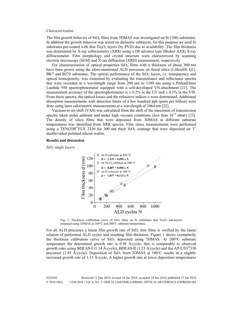
Fig. 1. Thickness calibration curve of SiO2 films on Si substrates and Ta2O5 sub-layers prepared using 3DMAS at 100°C and 200°C substrate temperature.
For all ALD processes a linear film growth rate of SiO2 thin films is verified by the linear relation of performed ALD cycles and resulting film thickness. Figure 1 shows exemplarily the thickness calibration curve of SiO2 deposited using 3DMAS. At 200°C substrate temperature the determined growth rate is 0.98 Å/cycle, that is comparable to observed growth rates using BDEAS-I (1.14 Å/cycle), BDEAS-II (1.23 Å/cycle) and the AP-LTO®330 precursor (1.85 Å/cycle). Deposition of SiO2 from 3DMAS at 100°C results in a slightly increased growth rate of 1.13 Å/cycle. A higher growth rate at lower deposition temperatures
#255642 Received 11 Dec 2015; revised 18 Jan 2016; accepted 18 Jan 2016; published 27 Jan 2016 © 2016 OSA 1 Feb 2016 | Vol. 6, No. 2 | DOI:10.1364/OME.6.000660 | OPTICAL MATERIALS EXPRESS 664
was also found for BDEAS-I. This has been attributed to decreased precursor chemisorption at higher temperatures due to a lower –OH density after the plasma step [15].
ALD nucleation and growth is generally affected by different substrate materials [24, 25]. For application of ALD SiO2 layers in optical multilayer stacks, the linear film growth needs to be demonstrated also on dielectric coatings. Figure 1 shows that SiO2 films have the same constant growth behavior on Ta2O5 pre-coated Si substrates. In conclusion, the thickness of SiO2 layers in e.g. dielectric layer stacks can be controlled easily by counting ALD cycles. Slightly deviating growth behavior of SiO2 on Si and the dielectric sub-layer can be attributed to a substrate depending delay in thin film nucleation in the initial stages of the growth [26].
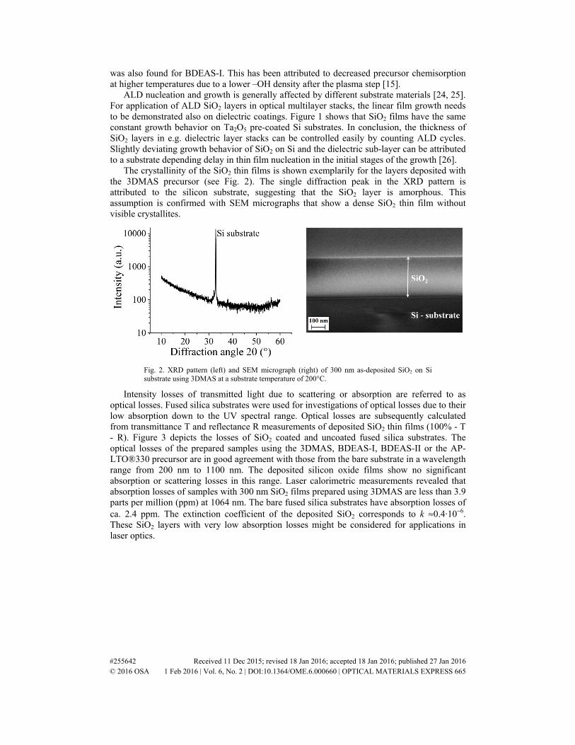
The crystallinity of the SiO2 thin films is shown exemplarily for the layers deposited with the 3DMAS precursor (see Fig. 2). The single diffraction peak in the XRD pattern is attributed to the silicon substrate, suggesting that the SiO2 layer is amorphous. This assumption is confirmed with SEM micrographs that show a dense SiO2 thin film without visible crystallites.
Fig. 2. XRD pattern (left) and SEM micrograph (right) of 300 nm as-deposited SiO2 on Si substrate using 3DMAS at a substrate temperature of 200°C.
Intensity losses of transmitted light due to scattering or absorption are referred to as optical losses. Fused silica substrates were used for investigations of optical losses due to their low absorption down to the UV spectral range. Optical losses are subsequently calculated from transmittance T and reflectance R measurements of deposited SiO2 thin films (100% - T - R). Figure 3 depicts the losses of SiO2 coated and uncoated fused silica substrates. The optical losses of the prepared samples using the 3DMAS, BDEAS-I, BDEAS-II or the AP-LTO®330 precursor are in good agreement with those from the bare substrate in a wavelength range from 200 nm to 1100 nm. The deposited silicon oxide films show no significant absorption or scattering losses in this range. Laser calorimetric measurements revealed that absorption losses of samples with 300 nm SiO2 films prepared using 3DMAS are less than 3.9 parts per million (ppm) at 1064 nm. The bare fused silica substrates have absorption losses of ca. 2.4 ppm. The extinction coefficient of the deposited SiO2 corresponds to k ≈0.4·10−6. These SiO2 layers with very low absorption losses might be considered for applications in laser optics.
#255642 Received 11 Dec 2015; revised 18 Jan 2016; accepted 18 Jan 2016; published 27 Jan 2016 © 2016 OSA 1 Feb 2016 | Vol. 6, No. 2 | DOI:10.1364/OME.6.000660 | OPTICAL MATERIALS EXPRESS 665
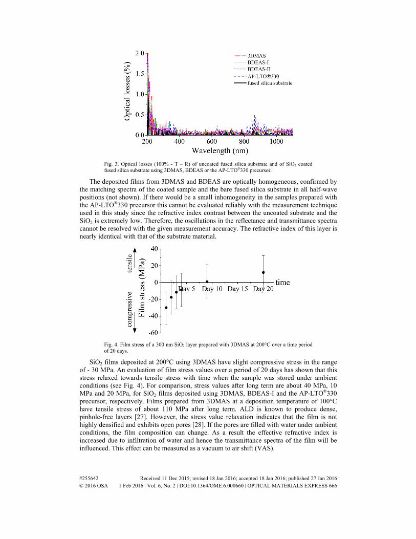
Fig. 3. Optical losses (100% - T – R) of uncoated fused silica substrate and of SiO2 coated fused silica substrate using 3DMAS, BDEAS or the AP-LTO®330 precursor.
The deposited films from 3DMAS and BDEAS are optically homogeneous, confirmed by the matching spectra of the coated sample and the bare fused silica substrate in all half-wave positions (not shown). If there would be a small inhomogeneity in the samples prepared with the AP-LTO®330 precursor this cannot be evaluated reliably with the measurement technique used in this study since the refractive index contrast between the uncoated substrate and the SiO2 is extremely low. Therefore, the oscillations in the reflectance and transmittance spectra cannot be resolved with the given measurement accuracy. The refractive index of this layer is nearly identical with that of the substrate material.
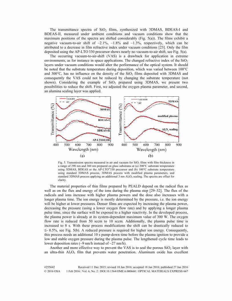
Fig. 4. Film stress of a 300 nm SiO2 layer prepared with 3DMAS at 200°C over a time period of 20 days.
SiO2 films deposited at 200°C using 3DMAS have slight compressive stress in the range of - 30 MPa. An evaluation of film stress values over a period of 20 days has shown that this stress relaxed towards tensile stress with time when the sample was stored under ambient conditions (see Fig. 4). For comparison, stress values after long term are about 40 MPa, 10 MPa and 20 MPa, for SiO2 films deposited using 3DMAS, BDEAS-I and the AP-LTO®330 precursor, respectively. Films prepared from 3DMAS at a deposition temperature of 100°C have tensile stress of about 110 MPa after long term. ALD is known to produce dense, pinhole-free layers [27]. However, the stress value relaxation indicates that the film is not highly densified and exhibits open pores [28]. If the pores are filled with water under ambient conditions, the film composition can change. As a result the effective refractive index is increased due to infiltration of water and hence the transmittance spectra of the film will be influenced. This effect can be measured as a vacuum to air shift (VAS).
#255642 Received 11 Dec 2015; revised 18 Jan 2016; accepted 18 Jan 2016; published 27 Jan 2016 © 2016 OSA 1 Feb 2016 | Vol. 6, No. 2 | DOI:10.1364/OME.6.000660 | OPTICAL MATERIALS EXPRESS 666
The transmittance spectra of SiO2 films, synthesized with 3DMAS, BDEAS-I and BDEAS-II, measured under ambient conditions and vacuum conditions show that the maximum positions of the spectra are shifted considerably (Fig. 5(a)). The films exhibit a negative vacuum-to-air shift of −2.1%, −1.8% and −1.3%, respectively, which can be attributed to a decrease in film refractive index under vacuum conditions [23]. Only the film deposited using the AP-LTO 330 precursor shows nearly no vacuum-to-air shift, see Fig. 5(a).
The occurring vacuum-to-air-shift (VAS) is a drawback for application in extreme environments, as for instance in space applications. The changed refractive index of the SiO2 layers under vacuum conditions would alter the performance of the optical system. It should be noted that the substrate temperature during deposition, which was varied between 100°C and 300°C, has no influence on the density of the SiO2 films deposited with 3DMAS and consequently the VAS could not be reduced by changing the substrate temperature (not shown). Considering the example of SiO2 prepared using 3DMAS, we present two possibilities to reduce the shift. First, we adjusted the oxygen plasma parameter, and second, an alumina sealing layer was applied.
Fig. 5. Transmission spectra measured in air and vacuum for SiO2 films with film thickness in a range of 290 nm and 360 nm prepared on glass substrates at (a) 200°C substrate temperature using 3DMAS, BDEAS or the AP-LTO®330 precursor and (b) 100°C substrate temperature using standard 3DMAS process, 3DMAS process with modified plasma parameters, and standard 3DMAS process applying an additional 3 nm Al2O3 sealing. The spectra are offset for clarity.
The material properties of thin films prepared by PEALD depend on the radical flux as well as on the flux and energy of the ions during the plasma step [29–32]. The flux of the radicals and ions increase with higher plasma powers and the dose also increases with a longer plasma time. The ion energy is mostly determined by the pressure, i.e. the ion energy will be higher at lower pressures. Denser films are expected by increasing the plasma power, decreasing the pressure (using a lower oxygen flow rate) and by applying a longer plasma pulse time, since the surface will be exposed to a higher reactivity. In the developed process, the plasma power is already at its system-dependent maximum value of 300 W. The oxygen flow rate is reduced from 50 sccm to 10 sccm. Additionally, the plasma pulse time is increased to 8 s. With these process modifications the shift can be drastically reduced to ≤- 0.5%, see Fig. 5(b). A reduced pressure is required for higher ion energy. Consequently, this process needs an additional 10 s pump-down time before the plasma ignition to provide a low and stable oxygen pressure during the plasma pulse. The lengthened cycle time leads to lower deposition rates (~9 nm/h instead of ~27 nm/h).
Another and more effective way to prevent the VAS is to seal the porous SiO2 layer with an ultra-thin Al2O3 film that prevents water penetration. Aluminum oxide has excellent
#255642 Received 11 Dec 2015; revised 18 Jan 2016; accepted 18 Jan 2016; published 27 Jan 2016 © 2016 OSA 1 Feb 2016 | Vol. 6, No. 2 | DOI:10.1364/OME.6.000660 | OPTICAL MATERIALS EXPRESS 667
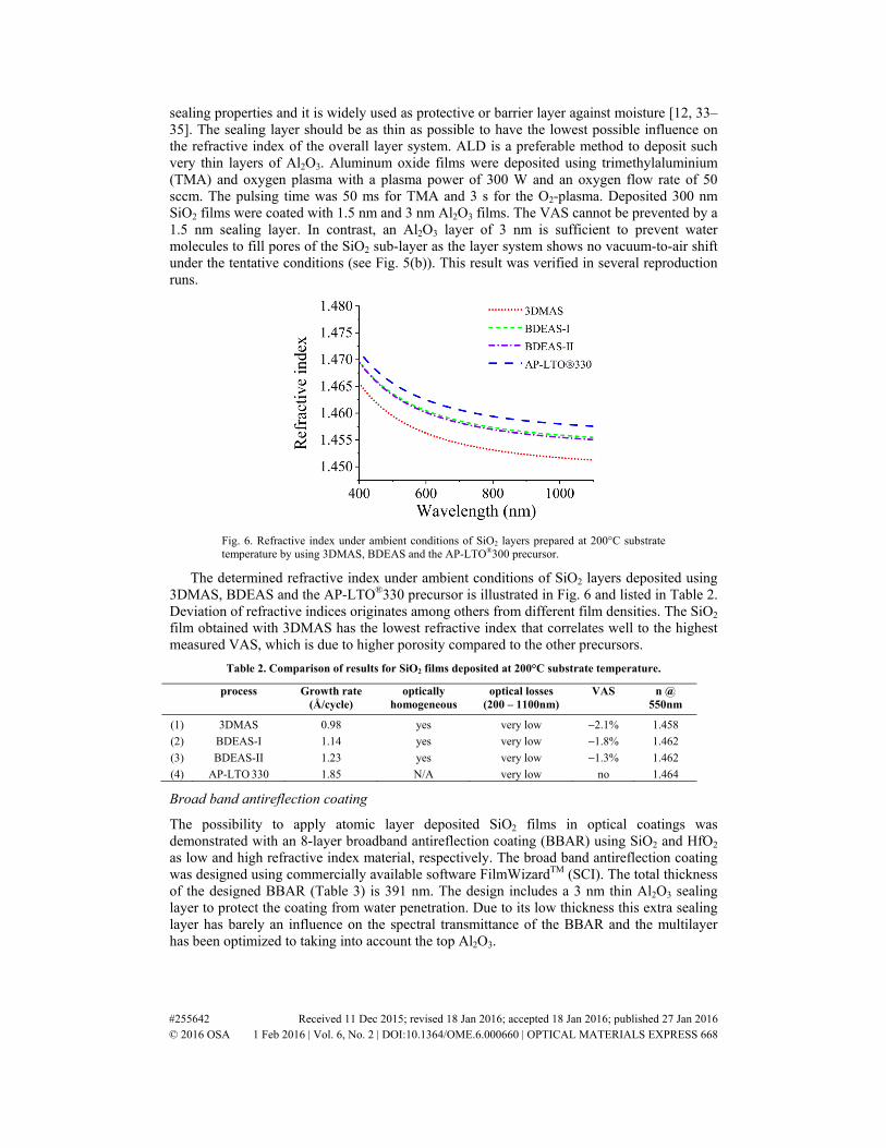
sealing properties and it is widely used as protective or barrier layer against moisture [12, 33–35]. The sealing layer should be as thin as possible to have the lowest possible influence on the refractive index of the overall layer system. ALD is a preferable method to deposit such very thin layers of Al2O3. Aluminum oxide films were deposited using trimethylaluminium (TMA) and oxygen plasma with a plasma power of 300 W and an oxygen flow rate of 50 sccm. The pulsing time was 50 ms for TMA and 3 s for the O2-plasma. Deposited 300 nm SiO2 films were coated with 1.5 nm and 3 nm Al2O3 films. The VAS cannot be prevented by a 1.5 nm sealing layer. In contrast, an Al2O3 layer of 3 nm is sufficient to prevent water molecules to fill pores of the SiO2 sub-layer as the layer system shows no vacuum-to-air shift under the tentative conditions (see Fig. 5(b)). This result was verified in several reproduction runs.
Fig. 6. Refractive index under ambient conditions of SiO2 layers prepared at 200°C substrate temperature by using 3DMAS, BDEAS and the AP-LTO®300 precursor.
The determined refractive index under ambient conditions of SiO2 layers deposited using 3DMAS, BDEAS and the AP-LTO®330 precursor is illustrated in Fig. 6 and listed in Table 2. Deviation of refractive indices originates among others from different film densities. The SiO2 film obtained with 3DMAS has the lowest refractive index that correlates well to the highest measured VAS, which is due to higher porosity compared to the other precursors.
Table 2. Comparison of results for SiO2 films deposited at 200°C substrate temperature.
process Growth rate
(Å/cycle) optically
homogeneous optical losses
(200 – 1100nm) VAS n @
550nm
(1) 3DMAS 0.98 yes very low −2.1% 1.458 (2) BDEAS-I 1.14 yes very low −1.8% 1.462 (3) BDEAS-II 1.23 yes very low −1.3% 1.462 (4) AP-LTO 330 1.85 N/A very low no 1.464
Broad band antireflection coating
The possibility to apply atomic layer deposited SiO2 films in optical coatings was demonstrated with an 8-layer broadband antireflection coating (BBAR) using SiO2 and HfO2 as low and high refractive index material, respectively. The broad band antireflection coating was designed using commercially available software FilmWizardTM (SCI). The total thickness of the designed BBAR (Table 3) is 391 nm. The design includes a 3 nm thin Al2O3 sealing layer to protect the coating from water penetration. Due to its low thickness this extra sealing layer has barely an influence on the spectral transmittance of the BBAR and the multilayer has been optimized to taking into account the top Al2O3.
#255642 Received 11 Dec 2015; revised 18 Jan 2016; accepted 18 Jan 2016; published 27 Jan 2016 © 2016 OSA 1 Feb 2016 | Vol. 6, No. 2 | DOI:10.1364/OME.6.000660 | OPTICAL MATERIALS EXPRESS 668
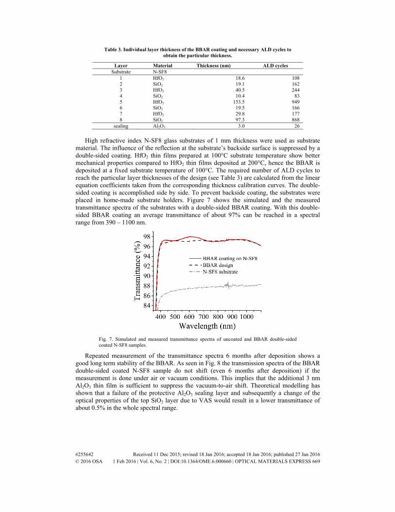
Table 3. Individual layer thickness of the BBAR coating and necessary ALD cycles to obtain the particular thickness.
Layer Material Thickness (nm) ALD cycles Substrate N-SF8
1 HfO2 18.6 108 2 SiO2 19.1 162 3 HfO2 40.5 244 4 SiO2 10.4 83 5 HfO2 153.5 949 6 SiO2 19.5 166 7 HfO2 29.8 177 8 SiO2 97.3 868
sealing Al2O3 3.0 26
High refractive index N-SF8 glass substrates of 1 mm thickness were used as substrate
material. The influence of the reflection at the substrate’s backside surface is suppressed by a double-sided coating. HfO2 thin films prepared at 100°C substrate temperature show better mechanical properties compared to HfO2 thin films deposited at 200°C, hence the BBAR is deposited at a fixed substrate temperature of 100°C. The required number of ALD cycles to reach the particular layer thicknesses of the design (see Table 3) are calculated from the linear equation coefficients taken from the corresponding thickness calibration curves. The double-sided coating is accomplished side by side. To prevent backside coating, the substrates were placed in home-made substrate holders. Figure 7 shows the simulated and the measured transmittance spectra of the substrates with a double-sided BBAR coating. With this double-sided BBAR coating an average transmittance of about 97% can be reached in a spectral range from 390 – 1100 nm.
Fig. 7. Simulated and measured transmittance spectra of uncoated and BBAR double-sided coated N-SF8 samples.
Repeated measurement of the transmittance spectra 6 months after deposition shows a good long term stability of the BBAR. As seen in Fig. 8 the transmission spectra of the BBAR double-sided coated N-SF8 sample do not shift (even 6 months after deposition) if the measurement is done under air or vacuum conditions. This implies that the additional 3 nm Al2O3 thin film is sufficient to suppress the vacuum-to-air shift. Theoretical modelling has shown that a failure of the protective Al2O3 sealing layer and subsequently a change of the optical properties of the top SiO2 layer due to VAS would result in a lower transmittance of about 0.5% in the whole spectral range.
#255642 Received 11 Dec 2015; revised 18 Jan 2016; accepted 18 Jan 2016; published 27 Jan 2016 © 2016 OSA 1 Feb 2016 | Vol. 6, No. 2 | DOI:10.1364/OME.6.000660 | OPTICAL MATERIALS EXPRESS 669
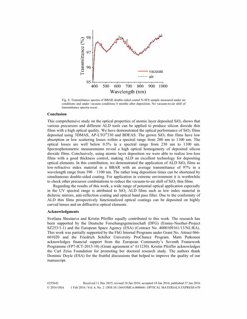
Fig. 8. Transmittance spectra of BBAR double-sided coated N-SF8 sample measured under air conditions and under vacuum conditions 6 months after deposition. No vacuum-to-air shift of transmittance spectra occur.
Conclusion
This comprehensive study on the optical properties of atomic layer deposited SiO2 shows that various precursors and different ALD tools can be applied to produce silicon dioxide thin films with a high optical quality. We have demonstrated the optical performance of SiO2 films deposited using 3DMAS, AP-LTO®330 and BDEAS. The grown SiO2 thin films have low absorption or low scattering losses within a spectral range from 200 nm to 1100 nm. The optical losses are well below 0.5% in a spectral range from 230 nm to 1100 nm. Spectrophotometric measurements reveal a high optical homogeneity of deposited silicon dioxide films. Conclusively, using atomic layer deposition we were able to realize low-loss films with a good thickness control, making ALD an excellent technology for depositing optical elements. In this contribution, we demonstrated the application of ALD SiO2 films as low-refractive index material in a BBAR with an average transmittance of 97% in a wavelength range from 390 – 1100 nm. The rather long deposition times can be shortened by simultaneous double-sided coating. For application in extreme environment it is worthwhile to check other precursor combinations to reduce the vacuum-to-air shift of SiO2 thin films.
Regarding the results of this work, a wide range of potential optical application especially in the UV spectral range is attributed to SiO2 ALD films such as low index material in dichroic mirrors, anti-reflection coating and optical band pass filter. Due to the conformity of ALD thin films prospectively functionalized optical coatings can be deposited on highly curved lenses and on diffractive optical elements.
Acknowledgments
Svetlana Shestaeva and Kristin Pfeiffer equally contributed to this work. The research has been supported by the Deutsche Forschungsgemeinschaft (DFG) (Emmy-Noether-Project SZ253/1-1) and the European Space Agency (ESA) (Contract No. 4000109161/13/NL/RA). This work was partially supported by the FhG Internal Programs under Grant No. Attract 066-601020 and the Friedrich Schiller University ProChance Program. Matti Putkonen acknowledges financial support from the European Community’s Seventh Framework Programme (FP7-ICT-2013-10) (Grant agreement n° 611230). Kristin Pfeiffer acknowledges the Carl Zeiss Foundation for promoting her doctoral research study. The authors thank Dominic Doyle (ESA) for the fruitful discussions that helped to improve the quality of our manuscript.
#255642 Received 11 Dec 2015; revised 18 Jan 2016; accepted 18 Jan 2016; published 27 Jan 2016 © 2016 OSA 1 Feb 2016 | Vol. 6, No. 2 | DOI:10.1364/OME.6.000660 | OPTICAL MATERIALS EXPRESS 670