Embed Size (px)
Citation preview

1/18
www.rohm.com 2015.1 - Rev.E© 2015 ROHM Co., Ltd. All rights reserved.
Compact Headphone Amplifiers
Headphone Amplifier Designed for 0.93V Low Voltage Operation BU7150NUV
Description BU7150NUV is Audio Amplifier designed for Single-cell battery operated audio products (VDD = 0.93 ~ 3.5V, at Ta=0~85°C). BU7150NUV can be selected in single-ended mode for stereo headphone and BTL mode for mono speaker operations. For BU7150NUV at VDD = 1.5V, THD+N = 1%, the output power is 14mW at RL = 16Ω in single-ended mode and the output power is 85mW at RL = 8Ω in BTL mode.
Features
1) Wide battery operation Voltage (0.93V~3.5V, Ta=0~85°C) (1.03V~3.5V, Ta= -40~85°C) 2) BU7150NUV can be selected in single-ended mode for stereo headphone and BTL mode for mono speaker operation 3) Unity-gain stability 4) Click and pop-noise reduction circuit built-in 5) Shutdown mode(Low power mode) 6) High speed turn-on mute mode 7) Thermal shutdown protection circuit 8) Power-on reset circuit not sensed during start-up slew rate of supply voltage 9) Small package (VSON010V3030)
Applications Noise-canceling headphone, IC recorder, Mobile phone, PDA, Electronic toys etc..
Absolute Maximum Ratings (Ta=25)
Parameter Symbol Ratings Unit
Supply Voltage VDD 4.5 V
Input Voltage VIN VSS-0.3~VDD+0.3 V
Input Current IIN -10~10 mA
Power Dissipation PD 560 * mW
Storage Temperature Range TSTG -55~+150 °C
*For operating over 25°C, de-rate the value at 5.6mW/°C.
This value is for IC mounted on 74.2 mm x 74.2mm x 1.6mm glass-epoxy PCB of single-layer.
Operating conditions
Parameter Symbol Ratings
Unit Min. Typ. Max.
Operation Temperature Range TOPR -40 - 85 °C
Supply Voltage (Note 1,2) VDD 0.93 - 3.5 V
Note 1: If the supply voltage is 0.93V, BU7150NUV does not operate at less than 0°C.
If the supply voltage is more than 1.03V, BU7150NUV operates until -40°C.
(But, it is not the one which guarantees the standard value for electric characteristics.)
Note 2: Ripple in power supply line should not exceed 400mVP-P.(VDD=1.5 V, Ta=25°C )
No.15102EET01

Technical Note
2/18
BU7150NUV
www.rohm.com 2015.1 - Rev.E© 2015 ROHM Co., Ltd. All rights reserved.
Electrical characteristics
Ta=25°C, VDD=1.5V, f=1kHz, VSS=GND unless otherwise specified.
Parameter Symbol Limits
Unit Conditions Min. Typ. Max.
No Signal Operating Current IDD - 1 1.4 mA No load, No signal
Shutdown Current ISD - 3 9 µA SDB Pin=VSS
Mute Current IMUTE - 15 - µA MUTEB Pin=VSS, SE
Output Offset Voltage VOFS - 5 50 mV | VOUT1 – VOUT2 |, No signal
Maximum Output Power PO
70 85 - mW RL=8Ω, BTL, THD+N=1%
- 14 - mW RL=16Ω, SE, THD+N=1%
Total Harmonic Distortion +Noise THD+N
- 0.2 0.5 % 20kHz LPF, RL=8Ω, BTL, PO=25mW
- 0.1 0.5 % 20kHz LPF, RL=16Ω, SE,PO=5mW
Output Voltage Noise VNO - 10 - µVrms 20kHz LPF + A-weight
Crosstalk CT - 85 - dB RL=16Ω, SE, 1kHz BPF
Power Supply Rejection Ratio PSRR
- 62 - dB Ripple voltage=200mVP-P, RL=8Ω, BTL, CBYPASS=4.7µF
- 66 - dB Ripple voltage=200mVP-P, RL=16Ω, SE, CBYPASS=4.7µF
Input Logic High Level VIH 0.7 - - V MUTEB Pin, SDB Pin
Input Logic Low Level VIL - - 0.3 V MUTEB Pin, SDB Pin
“BTL” is BTL-mode when MODE Pin = VDD, “SE” is single-ended mode when MODE Pin = VSS. Turn-on time in BTL mode is about 11 times faster than single-ended mode. Also, BTL mode does not have MUTE mode. When MUTEB Pin = VSS, then it will be shutdown mode.
Block diagram
Fig. 1 Block diagram
Bias
Generator
Control Logic
IN1
BYPASS
MUTEB
VDD
MODE
OUT1SDB
IN2
OUT2
VSS
1
2
3
4
5
10
9
8
7
6
TOP VIEW

Technical Note
3/18
BU7150NUV
www.rohm.com 2015.1 - Rev.E© 2015 ROHM Co., Ltd. All rights reserved.
Electrical characteristics waveform (Reference data)
Ta=25°C, f=1kHz, VSS=GND unless otherwise specified. Using circuits are Fig.34 and Fig.35.
Also, RL=16Ω for single ended mode, RL=8Ω for BTL mode)
VDD=1.5V, SE m ode
-70
-60
-50
-40
-30
-20
-10
0
10n 100n 1u 10u 100u 1m 10m 100m
TH
D+
N [d
B]
VDD=1.5V, Po=5m W,
SE m ode, BW<80kHz
-80
-70
-60
-50
-40
-30
-20
-10
0
10 100 1k 10k 100k
TH
D+
N [d
B]
VDD=1.2V, SE m ode
-60
-50
-40
-30
-20
-10
0
10n 100n 1u 10u 100u 1m 10m 100m
TH
D+
N [d
B]
VDD=1.2V, Po=2.5m W,
SE m ode, BW<80kHz
-80
-70
-60
-50
-40
-30
-20
-10
0
10 100 1k 10k 100k
TH
D+
N [d
B]
VDD=1.5V, BTL m ode
-70
-60
-50
-40
-30
-20
-10
0
10n 100n 1u 10u 100u 1m 10m 100m
TH
D+
N [d
B]
VDD=1.2V, BTL m ode
-60
-50
-40
-30
-20
-10
0
10n 100n 1u 10u 100u 1m 10m 100m
TH
D+
N [d
B]
VDD=1.5V, Po=25m W,
BTL m ode, BW<80kHz
-80
-70
-60
-50
-40
-30
-20
-10
0
10 100 1k 10k 100k
TH
D+
N [d
B]
VDD=1.2V, Po=10m W,
BTL m ode, BW<80kHz
-80
-70
-60
-50
-40
-30
-20
-10
0
10 100 1k 10k 100k
TH
D+
N [d
B]
Output Power [W]
Fig. 2 THD+N vs . Output Power
Output Power [W]
Fig. 3 THD+N vs . Output Power
Output Power [W]
Fig. 4 THD+N vs . Output Power
Output Power [W]
Fig. 5 THD+N vs . Output Power
Frequency [Hz]
Fig. 6 THD+N vs . Frequency
Frequency [Hz]
Fig. 7 THD+N vs . Frequency
Frequency [Hz]
Fig. 9 THD+N vs . Frequency
Frequency [Hz]
Fig. 8 THD+N vs . Frequency

Technical Note
4/18
BU7150NUV
www.rohm.com 2015.1 - Rev.E© 2015 ROHM Co., Ltd. All rights reserved.
VDD=1.5V, Po=5m W, SE m ode
-50
-40
-30
-20
-10
0
10
10 100 1k 10k 100k 1M
Ga
in [d
B]
VDD=1.5V, SE m ode
-100
-90
-80
-70
-60
-50
-40
-30
-20
-10
0
-100 -80 -60 -40 -20 0
Ou
tpu
t L
eve
l [d
BV
]
VDD=1.2V, SE m ode
-120
-100
-80
-60
-40
-20
0
-120 -100 -80 -60 -40 -20 0
Ou
tpu
t L
eve
l [d
BV
]
VDD=1.2V, Po=2.5m W, SE m ode
-50
-40
-30
-20
-10
0
10
10 100 1k 10k 100k 1M
Ga
in [d
B]
VDD=1.5V, BTL m ode
-100
-90
-80
-70
-60
-50
-40
-30
-20
-10
0
-100 -80 -60 -40 -20 0
Ou
tpu
t L
eve
l [d
BV
]
VDD=1.2V, BTL m ode
-120
-100
-80
-60
-40
-20
0
-120 -100 -80 -60 -40 -20 0
Ou
tpu
t L
eve
l [d
BV
]
VDD=1.5V, Po=25m W, BTL m ode
-50
-40
-30
-20
-10
0
10
10 100 1k 10k 100k 1M
Ga
in [d
B]
VDD=1.2V, Po=10m W, BTL m ode
-50
-40
-30
-20
-10
0
10
10 100 1k 10k 100k 1M
Ga
in [d
B]
Input Level [dBV]
Fig. 10 Output Level vs . Input Level
Input Level [dBV]
Fig. 11 Output Level vs . Input Level
Frequency [Hz]
Fig. 16 Gain vs . Frequency
Frequency [Hz]
Fig. 17 Gain vs . Frequency
Input Level [dBV]
Fig. 12 Output Level vs . Input Level
Input Level [dBV]
Fig. 13 Output Level vs . Input Level
Frequency [Hz]
Fig. 14 Gain vs . Frequency
Frequency [Hz]
Fig. 15 Gain vs . Frequency

Technical Note
5/18
BU7150NUV
www.rohm.com 2015.1 - Rev.E© 2015 ROHM Co., Ltd. All rights reserved.
SE m ode
0
20
40
60
80
100
120
140
0 1 2 3 4
Po
we
r [m
W]
THD+N = 10%
THD+N = 1%
BTL m ode
0
100
200
300
400
500
600
700
800
900
1000
0 1 2 3 4
Po
we
r [m
W]
THD+N = 10%
THD+N = 1%
BTL m ode
Zoom up
0
20
40
60
80
100
120
140
160
180
200
0.0 0.5 1.0 1.5 2.0
Po
we
r [m
W]
THD+N = 10%
THD+N = 1%
SE m ode
Zoom up
0
5
10
15
20
25
30
35
40
0.0 0.5 1.0 1.5 2.0
Po
we
r [m
W]
THD+N = 10%
THD+N = 1%
VDD=1.2V, Input=200m VP-P,
SE m ode, Input Term inated into 10Ω
-90
-80
-70
-60
-50
-40
-30
-20
-10
0
10 100 1k 10k 100k
PS
RR
[d
B]
VDD=1.5V, Input=200m VP-P,
SE m ode, Input Term inated into 10Ω
-90
-80
-70
-60
-50
-40
-30
-20
-10
0
10 100 1k 10k 100k
PS
RR
[d
B]
VDD=1.5V, Input=200m VP-P,
BTL m ode, Input Term inated into 10Ω
-90
-80
-70
-60
-50
-40
-30
-20
-10
0
10 100 1k 10k 100k
PS
RR
[d
B]
VDD=1.2V, Input=200m VP-P,
BTL m ode, Input Term inated into 10Ω
-90
-80
-70
-60
-50
-40
-30
-20
-10
0
10 100 1k 10k 100k
PS
RR
[d
B]
Supply Voltage [V]
Fig. 18 Maxim um output Power vs . Supply Voltage
Supply Voltage [V]
Fig. 19 Maxim um output Power vs . Supply Voltage
Supply Voltage [V]
Fig. 20 Maxim um output Power vs . Supply Voltage
Supply Voltage [V]
Fig. 21 Maxim um output Power vs . Supply Voltage
Frequency [Hz]
Fig. 22 PSRR vs . Frequency
Frequency [Hz]
Fig. 23 PSRR vs . Frequency
Frequency [Hz]
Fig. 24 PSRR vs . Frequency
Frequency [Hz]
Fig. 25 PSRR vs . Frequency
×××× :WC(PO=70m W
THD+N=1%)

Technical Note
6/18
BU7150NUV
www.rohm.com 2015.1 - Rev.E© 2015 ROHM Co., Ltd. All rights reserved.
SE m ode, Input=no s ignal
0
0.2
0.4
0.6
0.8
1
1.2
0 1 2 3 4
IDD
[m
A]
SE m ode, Input=no s ignal
0
0.5
1
1.5
2
2.5
3
3.5
4
4.5
0 1 2 3 4
ISD
[µ
A]
VDD=1.5V, Input=400m VP-P, SE m ode
-90
-85
-80
-75
-70
-65
-60
-55
-50
10 100 1k 10k 100k
MU
TE
Le
ve
l [d
B]
VDD=1.5V, Input=400m VP-P,
SE m ode, Input Term inated into 10Ω
-120
-110
-100
-90
-80
-70
-60
-50
-40
10 100 1k 10k 100k
Cro
ssta
lk [d
B]
VDD=1.2V, Input=400m VP-P,
SE m ode, Input Term inated into 10Ω
-120
-110
-100
-90
-80
-70
-60
-50
-40
10 100 1k 10k 100k
Cro
ssta
lk [d
B]
VDD=1.5V, SE m ode, 20kHz LPF + A-weight
-160
-140
-120
-100
-80
-60
-40
-20
0
10 100 1k 10k 100k
No
ise
Le
ve
l [d
BV
]
VDD=1.5V, BTL m ode, 20kHz LPF + A-weight
-160
-140
-120
-100
-80
-60
-40
-20
0
10 100 1k 10k 100k
No
ise
Le
ve
l [d
BV
]
Frequency [Hz]
Fig. 26 Cross talk vs . Frequency
Frequency [Hz]
Fig. 27 Cross talk vs . Frequency
Frequency [Hz]
Fig. 28 Noise Level vs . Frequency
Frequency [Hz]
Fig. 29 Noise Level vs . Frequency
Supply Voltage [V]
Fig. 30 IDD vs . Supply Voltage
Supply Voltage [V]
Fig. 31 ISD vs . Supply Voltage
Frequem cy [Hz]
Fig. 32 MUTE Level vs . Frequency
Technical Note
7/18
BU7150NUV
www.rohm.com 2015.1 - Rev.E© 2015 ROHM Co., Ltd. All rights reserved.
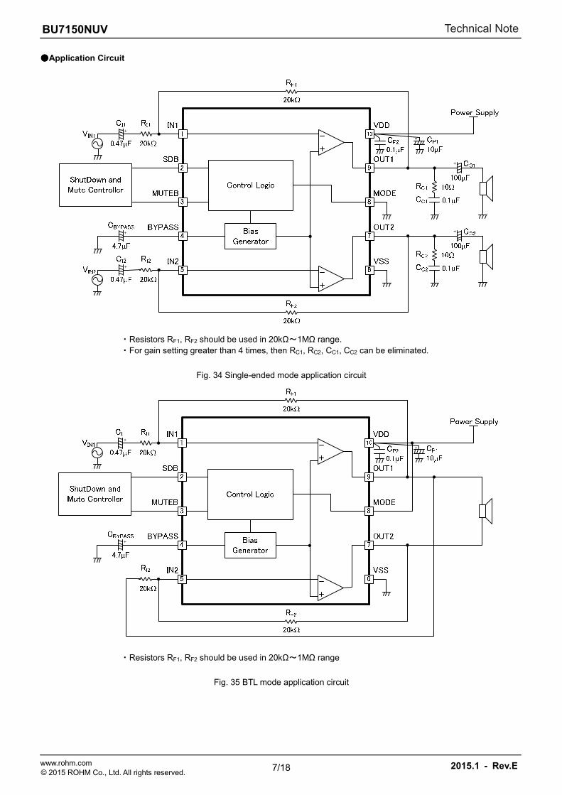
Application Circuit
・Resistors RF1, RF2 should be used in 20kΩ~1MΩ range.
・For gain setting greater than 4 times, then RC1, RC2, CC1, CC2 can be eliminated.
Fig. 34 Single-ended mode application circuit
・Resistors RF1, RF2 should be used in 20kΩ~1MΩ range
Fig. 35 BTL mode application circuit
+
++
++
++

Technical Note
8/18
BU7150NUV
www.rohm.com 2015.1 - Rev.E© 2015 ROHM Co., Ltd. All rights reserved.
Pin Configuration
Pin Description
No. Pin Name Function I/O equal circuit
1 IN1 Input Pin 1 A
2 SDB Shutdown Pin (OFF at L) C
3 MUTEB Mute Pin (Mute at L) C
4 BYPASS Bypass Pin D
5 IN2 Input Pin 2 A
6 VSS GND Pin -
7 OUT2 Output Pin 2 B
8 MODE Mode Select Pin (SE at VSS, BTL at VDD) A
9 OUT1 Output Pin 1 B
10 VDD Power Supply Pin -
IN1
BYPASS
MUTEB
VDD
MODE
OUT1SDB
IN2
OUT2
VSS
1
2
3
4
5
10
9
8
7
6
TOP VIEW
Thermal PAD
(Bottom)

Technical Note
9/18
BU7150NUV
www.rohm.com 2015.1 - Rev.E© 2015 ROHM Co., Ltd. All rights reserved.
I/O equal circuit (Fig. 36)
A B
C
D
Fig.36 I/O equal circuit
IN1IN2
MODE
VDD VDD
50Ω
VDDVDD
OUT1OUT2
SDBMUTEB
VDD
2kΩ
BYPASS
VDD
600kΩ 100kΩ
100kΩ
VDD
VDD

Technical Note
10/18
BU7150NUV
www.rohm.com 2015.1 - Rev.E© 2015 ROHM Co., Ltd. All rights reserved.
Functional descriptions
[Timing Chart]
BU7150NUV can control many mode states. “Active” is normal operation state for output signal. “Shutdown” is IC power down state for low power. “Mute” is Headphone amplifier power down state for low power and fast turn-on, because keeping BIAS voltage = VDD/2. “Turn on” and “Turn off” are sweep state.
Also, BU7150NUV has wait time for reduction of pop-sound at turn-on and turn-off. Turn-on wait time is 70msec from IN1 voltage = VDD/2. Turn-off wait time is 140msec from BYPASS voltage = 100mV. Please don't change SDB, MUTEB condition at 70msec and 140msec wait- time.
Fig. 38 Timing Chart (MODE = VDD: BTL- mode)
Fig. 37 Timing Chart (MODE = VSS: Single-ended mode)

Technical Note
11/18
BU7150NUV
www.rohm.com 2015.1 - Rev.E© 2015 ROHM Co., Ltd. All rights reserved.
[About Time until Signal Output]
BU7150NUV need wait-time for BIAS charge sweep time and pop-noise reduction. In the Fig. 37, Ts1 is BIAS charge sweep time from power on or SDB=H. Ts2 is time until signal output from power on or SDB=H. Also, in the Fig. 38, Tb1 is BIAS charge sweep time from power on. Tb2 is time until signal output from power on. Tb3 is BIAS charge sweep time from SDB=H. Tb4 is time until signal output from SDB=H. These values are decided equation (1) ~ (6). However, BIAS charge sweep time (Ts1, Tb1, Tb3) have uneven ±50%, and wait-time (70msec) is 40msec ~ 126msec for process parameter distribution. (Ta=25°C)
(1)[sec]102.5
CVDDTs1
6-
BYPASS ・・・ ×
×=
)2([sec]07.01Ts2Ts ・・・ +=
( )(3)[sec]
1027.5
C2VDDTb1
-6
BYPASS ・・・ ×
×+=
)4([sec]07.01Tb2Tb ・・・ +=
(5)[sec]1027.5
CVDDTb3
-6
BYPASS ・・・ ×
×=
)6([sec]07.03Tb4Tb ・・・ +=
In the Fig. 38, Tb1 and Tb3 is differ value, because BU7150NUV’s default is single-ended mode. BU7150NUV need BYPASS>100mV to recognize for BTL mode. Also, Td is delay time to CI1=VDD/2 from BYPASS=VDD/2. Td is decided by CI1, RI1, and RF1.
Fig. 39 Flow of Time until Signal Output

Technical Note
12/18
BU7150NUV
www.rohm.com 2015.1 - Rev.E© 2015 ROHM Co., Ltd. All rights reserved.
[Operation mode]
・Selecting operation mode
BU7150NUV has two OPAMP in the IC (Fig. 1). BU7150NUV is selected for BTL-mode for mono speaker and single-ended mode for stereo headphone operation. Mode is composed of external parts and internal control (Fig. 34, 35) BU7150NUV operates at single-ended mode when MODE pin (pin8) = 0V turn on. BTL mode is operated when MODE pin (pin8) = VDD turn on. BYPASS voltage = 100mV then operation mode is decided by internal comparator by detecting MODE voltage. The difference between Single-ended mode and BTL-mode is mentioned in the following table.
Parameter Single ended mode
MODE='VSS' BTL mode
MODE='VDD'
Mute function enable disenable
Bypass voltage turn on time [Ts1, Tb1, Tb3] (CBYPASS=4.7µF)
Ts1=2.82sec Tb1=598msec Tb3=256msec
Time until Signal Output [Ts2, Tb2, Tb4](CBYPASS=4.7µF)
Ts2=2.89sec Tb1=668msec Tb3=326msec
Maximum Output Power (THD=1%) 14mW 85mW
Total Harmonic Distortion + Noise 0.10% 0.20%
Power Supply Rejection Ratio 66dB 62dB
(Ta=25, VDD=1.5V, f=1kHz)

Technical Note
13/18
BU7150NUV
www.rohm.com 2015.1 - Rev.E© 2015 ROHM Co., Ltd. All rights reserved.
・Single-Ended mode
Single-ended mode can be use for stereo headphone amplifier using two internal amplifiers. BU7150NUV can select amplifier gain Av using external parts. (Fig. 34) Two amplifiers gain Av is decided by input resistance RI1, RI2 and feedback resistance RF1, RF2 aspect. Also, Please, use RF1, RF2 value in the range 20kΩ~1MΩ. Amplifier outputs (OUT1, OUT2) need coupling capacitors in single-ended mode operation. Coupling capacitors reduce DC-voltage at the output and to pass the audio signal. Single-ended mode has mute mode. Mute mode reduces pop noise and low power (typ. 15µA when MUTEB pin = Low. Rise time is high-speed though current consumption increases more than the state of the shutdown so that the state of the mute may keep the output level at the bias level. Mute level is decided by input resistance RI1, RI2 and feedback resistance RF1, RF2 and RL Mute level [dB] BU7150NUV needs phase-compensation circuit using external parts. (Fig. 34) But, for amplifier gain Av > 4 then phase compensation circuit may be eliminated.
・BTL mode
BTL mode can be used for mono speaker amplifier using two internal amplifiers. BU7150NUV can select amplifier gain Av using external parts. (Fig. 35) 1st stage gain is decided by selecting external parts. But 2nd stage gain = 1. 1st stage output signal and 2nd stage output signal are of same amplitude but phase difference of 180°. Amplifiers gain Av is decided by input resistance RI1 and feedback resistance RF1 aspect. Also, Please, use RF1, RF2 value in range of 20kΩ~1MΩ. BU7150NUV has no output pop noise at BTL mode operation, because output coupling capacitor is not charged. Therefore, BTL mode is faster by 11 times compared to single-ended mode. SDB pin and MUTEB pin are same function in BTL mode operation.
I
FV
R
RA −=
FI
L
RR
RLog20
+=
1I
1FV
R
R2A ∗=

Technical Note
14/18
BU7150NUV
www.rohm.com 2015.1 - Rev.E© 2015 ROHM Co., Ltd. All rights reserved.
[About Maximum Output Power]
Maximum output power of audio amplifier is reduced line impedance. Please, design to provide low impedance for the wiring between the power source and VDD pin of BU7150NUV. Also, please design to provide low impedance for the wiring between the GND and VSS pin of BU7150NUV.
VDD
Power source Impedance
GNDImpedance
SpeakerImpedance
Fig. 40 Line Impedance

Technical Note
15/18
BU7150NUV
www.rohm.com 2015.1 - Rev.E© 2015 ROHM Co., Ltd. All rights reserved.
[About a thermal PAD]
This product has a thermal PAD at the rear side of the package for heat dissipation and connecting it to GND plane will provide better heat dissipation. In the event that the IC will exceed its allowable heat dissipation, connect the thermal PAD to GND plane. Furthermore, heat dissipation properties can be improved by increasing the copper foil area of the printed board, which can also provide high allowable dissipation. Additionally, exceeding the allowable dissipation will lead to deterioration of the IC.
Please handle the thermal PAD according to the list shown below by a setting mode and supply voltage.
Note 3 Thermal PAD is not a GND terminal. Please give the GND electric potential from VSS terminal (6pin).
•
Figure 41. Power Dissipation vs Temperature
Figure 42. Handling of Thermal PAD Condition (BTL Mode)
Setting Allowable Dissipation Handling of Thermal PAD
SE mode (RL=16Ω ) I do not exceed it It is open or is connected to the GND pattern (Note 3)
SE mode
(RL=8Ω)
VDD < 2.9V
VDD ≥ 2.9V Exceed I am connected to the GND pattern (Note 3)
(I allow even opening by a condition. Reference Figure42)
Condition 1: When mounted on 1-layer 74.2 mm x 74.2 mm x 1.6 mm glass-epoxy PCB No copper foil (only mounting pattern)
Condition 2: When mounted on 4-layer 74.2 mm x 74.2 mm x 1.6 mm
glass-epoxy PCB6.28mm2 copper foil (back layer)
and 5,505mm2 copper foil (layers 2 & 3)
When mounted on 1-layer 74.2 mm x 74.2 mm x 1.6 mm glass-epoxy PCB No copper heat sink (only mounting pattern)
Operation Temperature : Topr [°C]
Po
we
r D
issip
atio
n :
Pd
[m
W]
Supply Voltage : VDD [V]
Ou
tpu
t P
ow
er
: P
o [m
W]

Technical Note
16/18
BU7150NUV
www.rohm.com 2015.1 - Rev.E© 2015 ROHM Co., Ltd. All rights reserved.
[How to select external parts for application]
・Power supply capacitor
Power supply capacitor is important for low noise and rejection of alternating current. Please use 10µF electrolytic or tantalum capacitor for low frequency and 0.1µF ceramic capacitor for high frequency nearer to BU7150NUV.
・BYPASS pin capacitor
BU7150NUV sweeps “Active” state after 70msec wait time after IN1 voltage = VDD/2. IN1 voltage are subordinated BYPASS voltage Ts. BYPASS voltage is subordinated BYPASS pin capacitor CBYPASS. Therefore, High speed turn on time is possible if CBYPASS is small value. But, pop noise may occur during turn on time. Therefore, CBYPASS need to be selected best value for application.

Technical Note
17/18
BU7150NUV
www.rohm.com 2015.1 - Rev.E© 2015 ROHM Co., Ltd. All rights reserved.
Notes for use
(1) Absolute Maximum Ratings An excess in the absolute maximum ratings, such as supply voltage, temperature range of operating conditions, etc., can break down devices, thus making impossible to identify breaking mode such as a short circuit or an open circuit. If any special mode exceeding the absolute maximum ratings is assumed, consideration should be given to take physical safety measures including the use of fuses, etc.
(2) Operating conditions These conditions represent a range within which characteristics can be provided approximately as expected. The electrical characteristics are guaranteed under the conditions of each parameter.
(3) Reverse connection of power supply connector The reverse connection of power supply connector can break down ICs. Take protective measures against the breakdown due to the reverse connection, such as mounting an external diode between the power supply and the IC’s power supply terminal.
(4) Power supply line Design PCB pattern to provide low impedance for the wiring between the power supply and the GND lines. In this regard, for the digital block power supply and the analog block power supply, even though these power supplies has the same level of potential, separate the power supply pattern for the digital block from that for the analog block, thus suppressing the diffraction of digital noises to the analog block power supply resulting from impedance common to the wiring patterns. For the GND line, give consideration to design the patterns in a similar manner. Furthermore, for all power supply terminals to ICs, mount a capacitor between the power supply and the GND terminal. At the same time, in order to use an electrolytic capacitor, thoroughly check to be sure the characteristics of the capacitor to be used present no problem including the occurrence of capacity dropout at a low temperature, thus determining the constant.
(5) GND voltage Make setting of the potential of the GND terminal so that it will be maintained at the minimum in any operating state. Furthermore, check to be sure no terminals are at a potential lower than the GND voltage including an actual electric transient.
(6) Short circuit between terminals and erroneous mounting In order to mount ICs on a set PCB, pay thorough attention to the direction and offset of the ICs. Erroneous mounting can break down the ICs. Furthermore, if a short circuit occurs due to foreign matters entering between terminals or between the terminal and the power supply or the GND terminal, the ICs can break down.
(7) Operation in strong electromagnetic field Be noted that using ICs in the strong electromagnetic field can malfunction them.
(8) Inspection with set PCB On the inspection with the set PCB, if a capacitor is connected to a low-impedance IC terminal, the IC can suffer stress. Therefore, be sure to discharge from the set PCB by each process. Furthermore, in order to mount or dismount the set PCB to/from the jig for the inspection process, be sure to turn OFF the power supply and then mount the set PCB to the jig. After the completion of the inspection, be sure to turn OFF the power supply and then dismount it from the jig. In addition, for protection against static electricity, establish a ground for the assembly process and pay thorough attention to the transportation and the storage of the set PCB.
(9) Input terminals In terms of the construction of IC, parasitic elements are inevitably formed in relation to potential. The operation of the parasitic element can cause interference with circuit operation, thus resulting in a malfunction and then breakdown of the input terminal. Therefore, pay thorough attention not to handle the input terminals, such as to apply to the input terminals a voltage lower than the GND respectively, so that any parasitic element will operate. Furthermore, do not apply a voltage to the input terminals when no power supply voltage is applied to the IC. In addition, even if the power supply voltage is applied, apply to the input terminals a voltage lower than the power supply voltage or within the guaranteed value of electrical characteristics.
(10) Ground wiring pattern If small-signal GND and large-current GND are provided, It will be recommended to separate the large-current GND pattern from the small-signal GND pattern and establish a single ground at the reference point of the set PCB so that resistance to the wiring pattern and voltage fluctuations due to a large current will cause no fluctuations in voltages of the small-signal GND. Pay attention not to cause fluctuations in the GND wiring pattern of external parts as well.
(11) External capacitor In order to use a ceramic capacitor as the external capacitor, determine the constant with consideration given to a degradation in the nominal capacitance due to DC bias and changes in the capacitance due to temperature, etc.
(12) About the rush current For ICs with more than one power supply, it is possible that rush current may flow instantaneously due to the internal powering sequence and delays. Therefore, give special consideration to power coupling capacitance, power wiring, width of GND wiring, and routing of wiring.
(13) Others In case of use this LSI, please peruse some other detail documents, we called ,Technical note, Functional description, Application note.

Technical Note
18/18
BU7150NUV
www.rohm.com 2015.1 - Rev.E© 2015 ROHM Co., Ltd. All rights reserved.
Ordering part number
B D 7 1 5 0 N U V - E 2
Part No. Part No.
Package
NUV : VSON010V3030
Packaging and forming specification
E2: Embossed tape and reel
(Unit : mm)
VSON010V3030
S
3.0±0.1
3.0
±0.1
1PIN MARK
1.0
MA
X
(0.2
2)
S0.08
0.0
2+
0.0
3
-0.0
2
610
51
0.4
±0.1
0.5
0.5
2.0±0.1
1.2
±0.1
0.25+0.05 -0.04
C0.25
∗ Order quantity needs to be multiple of the minimum quantity.
<Tape and Reel information>
Embossed carrier tapeTape
Quantity
Direction
of feed The direction is the 1pin of product is at the upper left when you hold
reel on the left hand and you pull out the tape on the right hand
3000pcs
E2
( )
Direction of feed
Reel1pin

DatasheetDatasheet
Notice-PGA-E Rev.001© 2015 ROHM Co., Ltd. All rights reserved.
Notice Precaution on using ROHM Products
1. Our Products are designed and manufactured for application in ordinary electronic equipments (such as AV equipment, OA equipment, telecommunication equipment, home electronic appliances, amusement equipment, etc.). If you intend to use our Products in devices requiring extremely high reliability (such as medical equipment (Note 1), transport equipment, traffic equipment, aircraft/spacecraft, nuclear power controllers, fuel controllers, car equipment including car accessories, safety devices, etc.) and whose malfunction or failure may cause loss of human life, bodily injury or serious damage to property (“Specific Applications”), please consult with the ROHM sales representative in advance. Unless otherwise agreed in writing by ROHM in advance, ROHM shall not be in any way responsible or liable for any damages, expenses or losses incurred by you or third parties arising from the use of any ROHM’s Products for Specific Applications.
(Note1) Medical Equipment Classification of the Specific Applications JAPAN USA EU CHINA
CLASSⅢ CLASSⅢ
CLASSⅡb CLASSⅢ
CLASSⅣ CLASSⅢ
2. ROHM designs and manufactures its Products subject to strict quality control system. However, semiconductor
products can fail or malfunction at a certain rate. Please be sure to implement, at your own responsibilities, adequate safety measures including but not limited to fail-safe design against the physical injury, damage to any property, which a failure or malfunction of our Products may cause. The following are examples of safety measures:
[a] Installation of protection circuits or other protective devices to improve system safety [b] Installation of redundant circuits to reduce the impact of single or multiple circuit failure
3. Our Products are designed and manufactured for use under standard conditions and not under any special or extraordinary environments or conditions, as exemplified below. Accordingly, ROHM shall not be in any way responsible or liable for any damages, expenses or losses arising from the use of any ROHM’s Products under any special or extraordinary environments or conditions. If you intend to use our Products under any special or extraordinary environments or conditions (as exemplified below), your independent verification and confirmation of product performance, reliability, etc, prior to use, must be necessary:
[a] Use of our Products in any types of liquid, including water, oils, chemicals, and organic solvents [b] Use of our Products outdoors or in places where the Products are exposed to direct sunlight or dust [c] Use of our Products in places where the Products are exposed to sea wind or corrosive gases, including Cl2,
H2S, NH3, SO2, and NO2
[d] Use of our Products in places where the Products are exposed to static electricity or electromagnetic waves [e] Use of our Products in proximity to heat-producing components, plastic cords, or other flammable items [f] Sealing or coating our Products with resin or other coating materials [g] Use of our Products without cleaning residue of flux (even if you use no-clean type fluxes, cleaning residue of
flux is recommended); or Washing our Products by using water or water-soluble cleaning agents for cleaning residue after soldering
[h] Use of the Products in places subject to dew condensation
4. The Products are not subject to radiation-proof design. 5. Please verify and confirm characteristics of the final or mounted products in using the Products. 6. In particular, if a transient load (a large amount of load applied in a short period of time, such as pulse. is applied,
confirmation of performance characteristics after on-board mounting is strongly recommended. Avoid applying power exceeding normal rated power; exceeding the power rating under steady-state loading condition may negatively affect product performance and reliability.
7. De-rate Power Dissipation (Pd) depending on Ambient temperature (Ta). When used in sealed area, confirm the actual
ambient temperature. 8. Confirm that operation temperature is within the specified range described in the product specification. 9. ROHM shall not be in any way responsible or liable for failure induced under deviant condition from what is defined in
this document.
Precaution for Mounting / Circuit board design 1. When a highly active halogenous (chlorine, bromine, etc.) flux is used, the residue of flux may negatively affect product
performance and reliability.
2. In principle, the reflow soldering method must be used on a surface-mount products, the flow soldering method must be used on a through hole mount products. If the flow soldering method is preferred on a surface-mount products, please consult with the ROHM representative in advance.
For details, please refer to ROHM Mounting specification

DatasheetDatasheet
Notice-PGA-E Rev.001© 2015 ROHM Co., Ltd. All rights reserved.
Precautions Regarding Application Examples and External Circuits 1. If change is made to the constant of an external circuit, please allow a sufficient margin considering variations of the
characteristics of the Products and external components, including transient characteristics, as well as static characteristics.
2. You agree that application notes, reference designs, and associated data and information contained in this document
are presented only as guidance for Products use. Therefore, in case you use such information, you are solely responsible for it and you must exercise your own independent verification and judgment in the use of such information contained in this document. ROHM shall not be in any way responsible or liable for any damages, expenses or losses incurred by you or third parties arising from the use of such information.
Precaution for Electrostatic
This Product is electrostatic sensitive product, which may be damaged due to electrostatic discharge. Please take proper caution in your manufacturing process and storage so that voltage exceeding the Products maximum rating will not be applied to Products. Please take special care under dry condition (e.g. Grounding of human body / equipment / solder iron, isolation from charged objects, setting of Ionizer, friction prevention and temperature / humidity control).
Precaution for Storage / Transportation 1. Product performance and soldered connections may deteriorate if the Products are stored in the places where:
[a] the Products are exposed to sea winds or corrosive gases, including Cl2, H2S, NH3, SO2, and NO2 [b] the temperature or humidity exceeds those recommended by ROHM [c] the Products are exposed to direct sunshine or condensation [d] the Products are exposed to high Electrostatic
2. Even under ROHM recommended storage condition, solderability of products out of recommended storage time period may be degraded. It is strongly recommended to confirm solderability before using Products of which storage time is exceeding the recommended storage time period.
3. Store / transport cartons in the correct direction, which is indicated on a carton with a symbol. Otherwise bent leads
may occur due to excessive stress applied when dropping of a carton. 4. Use Products within the specified time after opening a humidity barrier bag. Baking is required before using Products of
which storage time is exceeding the recommended storage time period.
Precaution for Product Label QR code printed on ROHM Products label is for ROHM’s internal use only.
Precaution for Disposition When disposing Products please dispose them properly using an authorized industry waste company.
Precaution for Foreign Exchange and Foreign Trade act Since concerned goods might be fallen under listed items of export control prescribed by Foreign exchange and Foreign trade act, please consult with ROHM in case of export.
Precaution Regarding Intellectual Property Rights 1. All information and data including but not limited to application example contained in this document is for reference
only. ROHM does not warrant that foregoing information or data will not infringe any intellectual property rights or any other rights of any third party regarding such information or data.
2. ROHM shall not have any obligations where the claims, actions or demands arising from the combination of the Products with other articles such as components, circuits, systems or external equipment (including software).
3. No license, expressly or implied, is granted hereby under any intellectual property rights or other rights of ROHM or any third parties with respect to the Products or the information contained in this document. Provided, however, that ROHM will not assert its intellectual property rights or other rights against you or your customers to the extent necessary to manufacture or sell products containing the Products, subject to the terms and conditions herein.
Other Precaution 1. This document may not be reprinted or reproduced, in whole or in part, without prior written consent of ROHM.
2. The Products may not be disassembled, converted, modified, reproduced or otherwise changed without prior written consent of ROHM.
3. In no event shall you use in any way whatsoever the Products and the related technical information contained in the Products or this document for any military purposes, including but not limited to, the development of mass-destruction weapons.
4. The proper names of companies or products described in this document are trademarks or registered trademarks of ROHM, its affiliated companies or third parties.

DatasheetDatasheet
Notice – WE Rev.001© 2015 ROHM Co., Ltd. All rights reserved.
General Precaution 1. Before you use our Pro ducts, you are requested to care fully read this document and fully understand its contents.
ROHM shall n ot be in an y way responsible or liabl e for fa ilure, malfunction or acci dent arising from the use of a ny ROHM’s Products against warning, caution or note contained in this document.
2. All information contained in this docume nt is current as of the issuing date and subj ect to change without any prior
notice. Before purchasing or using ROHM’s Products, please confirm the la test information with a ROHM sale s representative.
3. The information contained in this doc ument is provi ded on an “as is” basis and ROHM does not warrant that all
information contained in this document is accurate an d/or error-free. ROHM shall not be in an y way responsible or liable for any damages, expenses or losses incurred by you or third parties resulting from inaccuracy or errors of or concerning such information.