Embed Size (px)
Citation preview
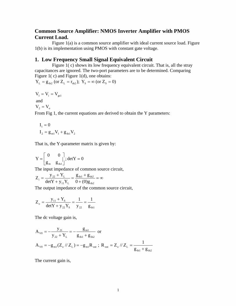
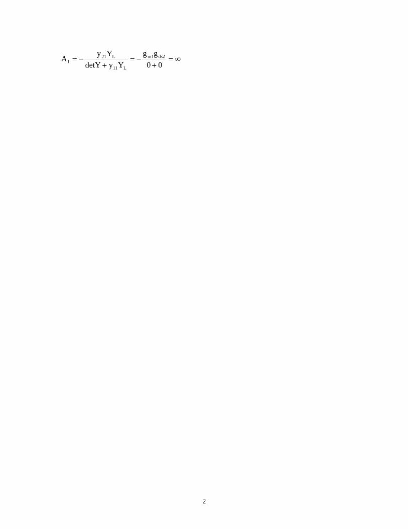
Common Source Amplifier: NMOS Inverter Amplifier with PMOS Current Load. Figure 1(a) is a common source amplifier with ideal current source load. Figure 1(b) is its implementation using PMOS with constant gate voltage. 1. Low Frequency Small Signal Equivalent Circuit Figure 1( c) shows its low frequency equivalent circuit. That is, all the stray capacitances are ignored. The two-port parameters are to be determined. Comparing
Figure 1( c) and Figure 1(d), one obtains:
From Fig 1, the current equations are derived to obtain the Y parameters:
ter matrix is given by:
on source circuit,
he output impedance of the common source circuit,
gs1i1 VVV ==
o2 V=
0
00 ⎤⎡
)0(or Z Y );r(or Z gY SSds2Lds2L =∞===
and V
1I =
2ds11m12 VgVgI += That is, the Y-parame
0detY ; gg
Yds1m
=⎥⎦
⎢⎣
=
The input impedance of comm
T
∞=+
+=
++
=ds2
ds2ds1
L11
L22i g)0(0
ggYydetY
YyZ
ds122S22
S11o g
1y1
YydetYYy
Z ==++
=
The dc voltage gain is,
The current gain is,
ds2ds1Looutoutm1Lom1V0 gg
1//ZR ; Rg)//Z(g
or gg
gYy
yA
+==−=−=
+−=
+−=
ZZ
ds2ds1
m1
L22
21V0
A
1
2
∞=+
−=+
−=00
ggYydetY
YyA ds2m1
L11
L21I
Vi
Vo
VDD
VG
VDD
Vo
ViM1 M1/MN
M2/MP
gm1vgs1 gds1 gds2Vo
Vi+
V1
-
+
V2
-
D1
S1
G1D2
S2
vgs1
(a) (b)
(c)
I1 I2
Y
+
V1
+
V2 YL
Zi Zo(d)
I1 I2
(2)
(1)
(4)
VSS
(5)
(3)
(9.6U/5.4U)
(25.8U/5.4U)
+
-
IP
IN
Figure 1. Common Source Amplifier: (a) ideal current source load, (b) PMOS current source load, ( c) low frequency small signal equivalent circuit, and (d) two-port representation.
3
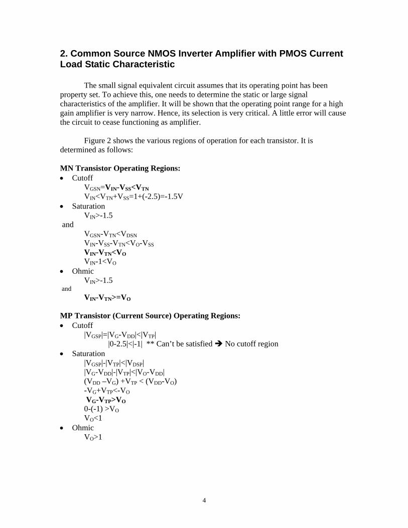
2. Common Source NMOS Inverter Amplifier with PMOS Current Load Static Characteristic The small signal equivalent circuit assumes that its operating point has been property set. To achieve this, one needs to determine the static or large signal characteristics of the amplifier. It will be shown that the operating point range for a high gain amplifier is very narrow. Hence, its selection is very critical. A little error will cause the circuit to cease functioning as amplifier.
Figure 2 shows the various regions of operation for each transistor. It is determined as follows:
MN Transistor Operating Regions: • Cutoff VGSN=VIN-VSS<VTN VIN<VTN+VSS=1+(-2.5)=-1.5V • Saturation VIN>-1.5 and VGSN-VTN<VDSN VIN-VSS-VTN<VO-VSS VIN-VTN<VO VIN-1<VO
• Ohmic VIN>-1.5 and VIN-VTN>=VO MP Transistor (Current Source) Operating Regions: • Cutoff |VGSP|=|VG-VDD|<|VTP| |0-2.5|<|-1| ** Can’t be satisfied No cutoff region • Saturation |VGSP|-|VTP|<|VDSP| |VG-VDD|-|VTP|<|VO-VDD| (VDD –VG) +VTP < (VDD-VO)
-VG+VTP<-VO VG-VTP>VO0-(-1) >VO
VO<1 • Ohmic VO>1
4
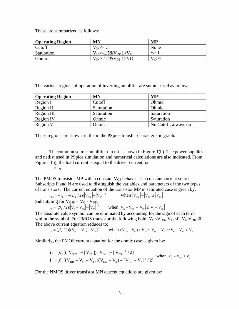
These are summarized as follows: Operating Region MN MP Cutoff VIN<-1.5 None Saturation VIN>-1.5&VIN-1<VO VO<1 Ohmic VIN>-1.5&VIN-1>VO VO>1 The various regions of operation of inverting amplifier are summarized as follows: Operating Region MN MP Region I Cutoff Ohmic Region II Saturation Ohmic Region III Saturation Saturation Region IV Ohmic Saturation Region V Ohmic No Cutoff, always on These regions are shown in the in the PSpice transfer characteristic graph. The common source amplifier circuit is shown in Figure 1(b). The power supplies and netlist used in PSpice simulation and numerical calculations are also indicated. From Figure 1(b), the load current is equal to the driver current, i.e. iP = iN The PMOS transistor MP with a constant VGS behaves as a constant current source. Subscripts P and N are used to distinguish the variables and parameters of the two types of transistors. The current equation of the transistor MP in saturated case is given by: i i V VDS P P GSP TP= − = − −( / )[ ]β 2 2 when V V VGSP TP DS− ≤ Substituting for VGSP = VG - VDD, i V VP P G DD TP= − −( / )[ ]β 2 2V when V V V V VG DD TP o DD− − ≤ − The absolute value symbol can be eliminated by accounting for the sign of each term within the symbol. For PMOS transistor the following hold: VG<VDD, VTP<0, Vo-VDD<0. The above current equation reduces to: when ( )i V VP P DD G TP= − +( / )[( ) ]β 2 2V V V V V V or V V VDD G TP DD o G TP o− + ≤ − − > Similarly, the PMOS current equation for the ohmic case is given by:
when V V ]2/)VV()VV)(VVV[(i
]2/|V||V||)V||V[(|i2
oDDoDDTPGDDPP
2DSDSTPGSPPP
−−−+−=
−−=
β
βVG TP− ≤ o
For the NMOS driver transistor MN current equations are given by:
5
i V VN N GSN TN= −( / )( )β 2 2 when V V VGSN TN DSN− ≤ , MN is saturated.
Substituting for VGSN = Vi - VSS, and VDSN=VO - VSS
i V V VN N SS TN
2= − −( / )( )β 2 i when V V V V V or V V VSS TN O SS TN Oi i− − ≤ − − ≤ , MN is saturated. Similarly, the NMOS current equation for the ohmic case is given by: i V V V V V V VN SS TN O SS O SS= − − − − −[( )( ) ( ) / ]i
2 2 when V V VTN Oi − > , MN is ohmic. The static characteristic is determined by equating the corresponding current equations at each voltage range: 1. Vi - VSS< VTN and VG-VTP=0-(-1)=1<Vo. The driver transistor MN is off, and MP is on (ohmic). Hence Vo = Vdd. 2. Vi - VSS > VTN , Vi-VTN <Vo, and (VG-VTP<Vo). The driver transistor MN is saturated, and the load transistor MP is ohmic.
]2/)VV()VV)(VVV[()VVV)(2/( 2ODDODDTPGDDP
2TNSSiN −−−+−=−− ββ
Solving for Vo, 2
TNSSiR2
TPGDDTPGO )VVV()VVV()VV(V −−−+−−−= β where PNR / βββ = 3. Vi - VSS > VTN , Vi -VTN <Vo, and VG-VTP>Vo. The driver transistor MN is saturated, and the load transistor MP is also saturated. 2
TPGDDP2
TNSSiN )VVV)(2/()VVV)(2/( +−=−− ββThis equation is independent of Vo, it is used to determine the operating point Vbias of the inverter. Solving for Vbias, RTPGDDTNSSbiasi /)VVV(VVVV β+−++== This value is only an approximation. The exact value is obtained from the PSpice simulation. The bias voltage corresponds to the input voltage Vi when the output voltage Vo=(VDD+ VSS )/2=(2.5-2.5)/2=0. 4. Vi - VSS > VTN, Vi -VTN > VO , and VG-VTP>Vo . The driver transistor MN is ohmic, and the load transistor MP is saturated. 2
TPGDDP2
SSOSSOTNSSiN )VVV)(2/(]2/)VV()VV)(VVV[( +−=−−−−− ββSolving for Vo,
R2
TPGDD2
TNSSiTNiO /)VVV()VVV()VV(V β+−−−−−−= 5. Vo= VSS , when the load transistor MP is off. It occurs when VGSP=VG-VDD>VTP. But for the given VG (=0) this can not happen. This is verified in the Pspice simulation. Figure 2 shows that VSS = -2.5 V can never be reached.
6
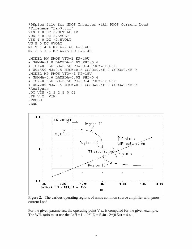
*PSpice file for NMOS Inverter with PMOS Current Load *Filename="Lab3.cir" VIN 1 0 DC 0VOLT AC 1V VDD 3 0 DC 2.5VOLT VSS 4 0 DC -2.5VOLT VG 5 0 DC 0VOLT M1 2 1 4 4 MN W=9.6U L=5.4U M2 2 5 3 3 MP W=25.8U L=5.4U .MODEL MN NMOS VTO=1 KP=40U + GAMMA=1.0 LAMBDA=0.02 PHI=0.6 + TOX=0.05U LD=0.5U CJ=5E-4 CJSW=10E-10 + U0=550 MJ=0.5 MJSW=0.5 CGSO=0.4E-9 CGDO=0.4E-9 .MODEL MP PMOS VTO=-1 KP=15U + GAMMA=0.6 LAMBDA=0.02 PHI=0.6 + TOX=0.05U LD=0.5U CJ=5E-4 CJSW=10E-10 + U0=200 MJ=0.5 MJSW=0.5 CGSO=0.4E-9 CGDO=0.4E-9 *Analysis .DC VIN -2.5 2.5 0.05 .TF V(2) VIN .PROBE .END
Figure 2. The various operating regions of nmos common source amplifier with pmos current l.oad For the given parameters, the operating point Vbias is computed for the given example. The W/L ratio must use the Leff = L - 2*LD = 5.4u - 2*(0.5u) = 4.4u.
7
16)-6/4.4E-6)(25.8E-(15E6)-6/4.4E-6)(9.6E-E40(
)L/W(K)L/(WK
PeffPeffP
NeffNNR ===β
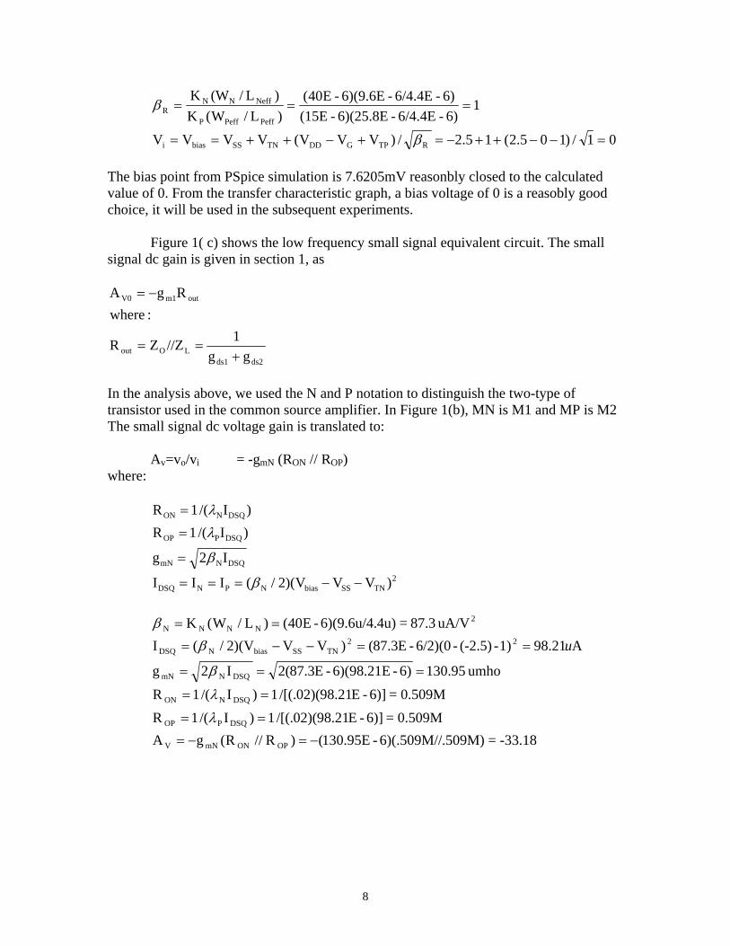
01/)105.2(15.2/)VVV(VVVV RTPGDDTNSSbiasi =−−++−=+−++== β The bias point from PSpice simulation is 7.6205mV reasonbly closed to the calculated value of 0. From the transfer characteristic graph, a bias voltage of 0 is a reasobly good choice, it will be used in the subsequent experiments. Figure 1( c) shows the low frequency small signal equivalent circuit. The small signal dc gain is given in section 1, as
e used the N and P notation to distinguish the two-type of
is M2
Av=vo/vi = -gmN (RON // ROP)
)
ds2ds1LOout
outm1V0
gg1//ZZR
:whereRgA
+==
−=
In the analysis above, wtransistor used in the common source amplifier. In Figure 1(b), MN is M1 and MP The small signal dc voltage gain is translated to: where: I/(1R DSQNON λ= )I/(1R DSQPOP λ=
DSQNmN I2g β=
( 2TNSSbiasNPNDSQ )VVV)(2/III −−=== β
2
NNNN uA/V 87.3=4u)6)(9.6u/4.-E40()L/W(K ==β A21.981)-(-2.5)-6/2)(0-E3.87()VVV)(2/(I 22
TNSSbiasNDSQ u==−−= β
umho 59.1306)-6)(98.21E-E3.87(2I2g DSQNmN === β
0.509M=6)]-E21.98)(02/[(.1)I/(1R0.509M=6)]-E21.98)(02/[(.1)I/(1R
DSQPOP
DSQNON
==
==
λ
λ
-33.18=.509M)6)(.509M//-E95.130()R//R(gA OPONmNV −=−=
8
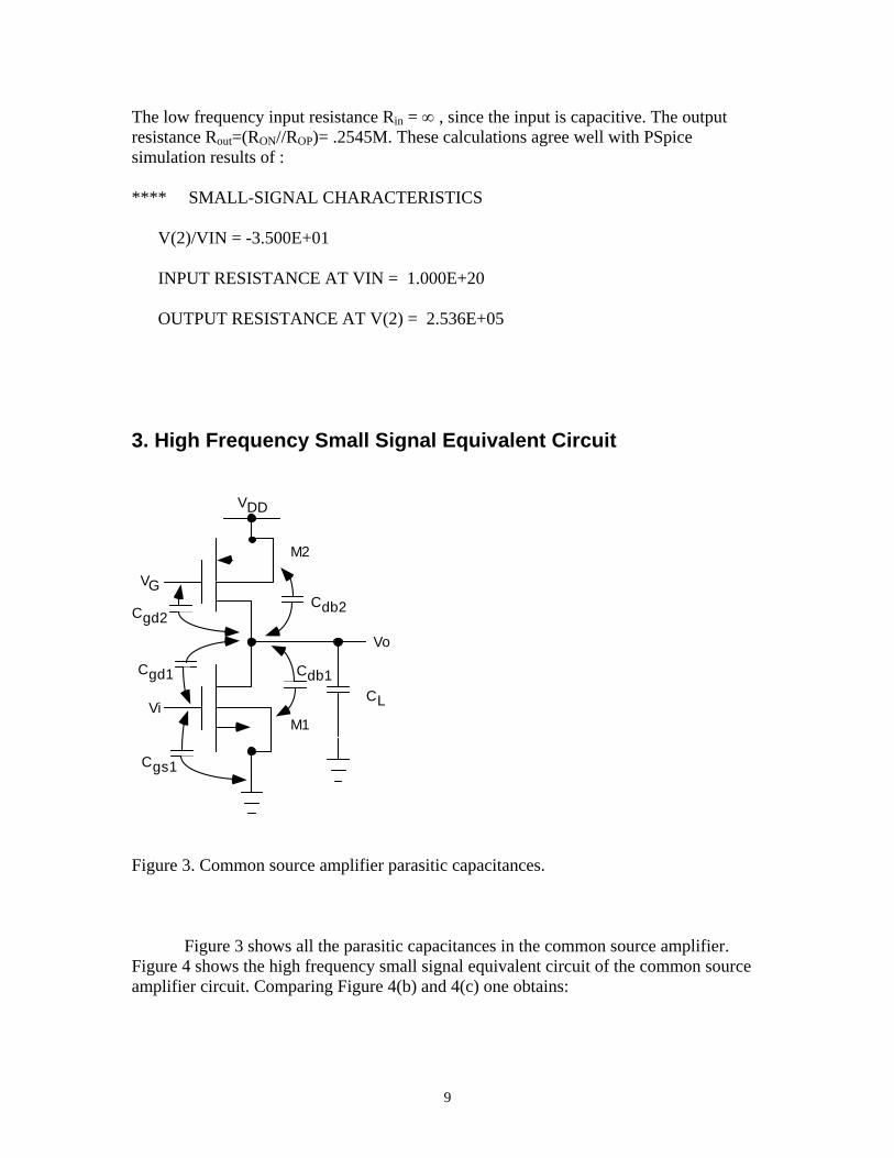
The low frequency input resistance Rin = ∞ , since the input is capacitive. The output resistance Rout=(RON//ROP)= .2545M. These calculations agree well with PSpice simulation results of : **** SMALL-SIGNAL CHARACTERISTICS V(2)/VIN = -3.500E+01 INPUT RESISTANCE AT VIN = 1.000E+20 OUTPUT RESISTANCE AT V(2) = 2.536E+05
3. High Frequency Small Signal Equivalent Circuit
VG
VDD
Vo
ViM1
M2
CL
Cdb2
Cgd1
Cgd2
Cdb1
Cgs1
Figure 3. Common source amplifier parasitic capacitances. Figure 3 shows all the parasitic capacitances in the common source amplifier. Figure 4 shows the high frequency small signal equivalent circuit of the common source amplifier circuit. Comparing Figure 4(b) and 4(c) one obtains:
9
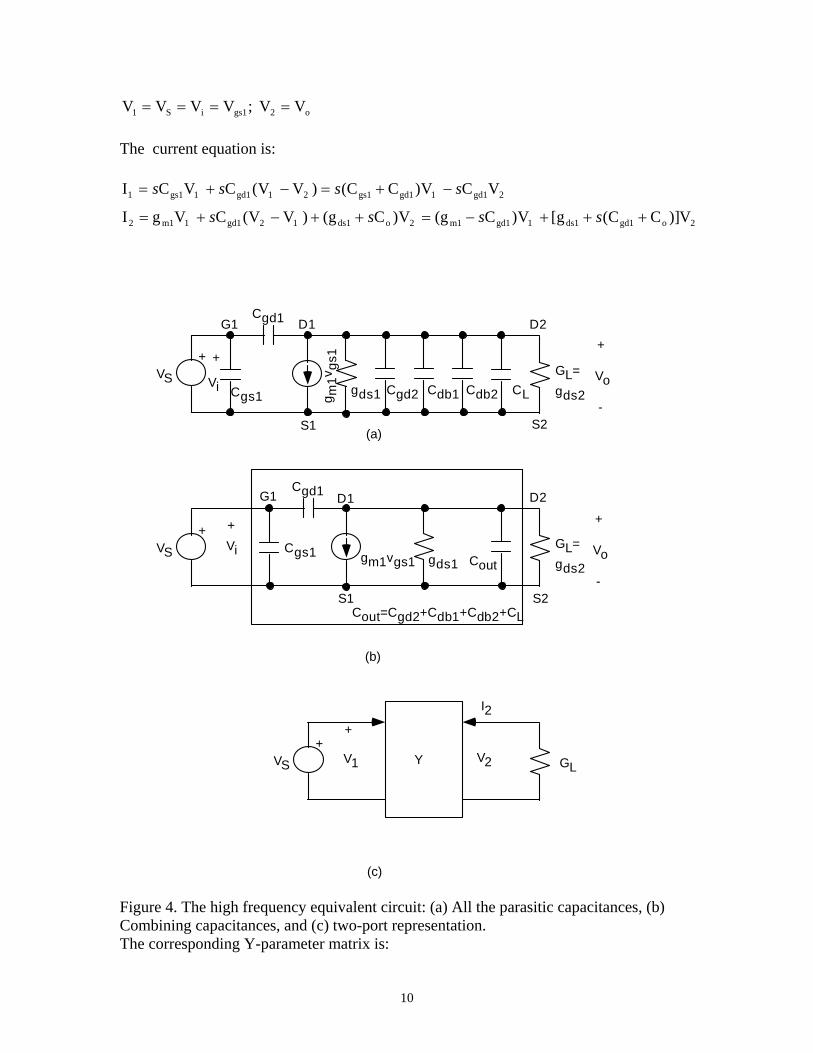
o2gs1iS1 VV ;VVVV ==== The current equation is:
2ogd1ds11gd1m12ods112gd11m12
2gd11gd1gs121gd11gs11
V)]CC(g[V)Cg(V)Cg()VV(CVgI
VCV)CC()VV(CVCI
+++−=++−+=
−+=−+=
ssss
ssss
Vi
Cgd1
Cgs1 gds1GL=gds2
gm1vgs1 Cout
G1 D1
S1
D2
S2Cout=Cgd2+Cdb1+Cdb2+CL
(b)
+
g m1v
gs1
Cgd1
Cgs1 gds1 Cdb1 Cdb2 CL
GL=gds2
G1 D1
S1
D2
S2
Y
(a)
V1
+
V2 GL
I2
(c)
+
Vi
+
-
Vo
+
-
Vo
Cgd2
+VS
+VS
+VS
igure 4. The high frequency equivalent circuit: (a) All the parasitic capacitances, (b) F
Combining capacitances, and (c) two-port representation. The corresponding Y-parameter matrix is:
10
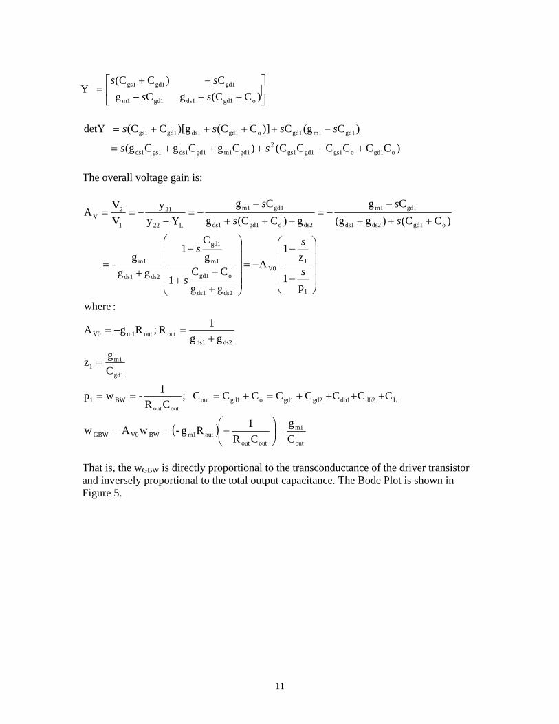
The overall voltage gain is:
nd inversely proportional to the total output capacitance. The Bode Plot is shown in igure 5.
⎥⎦
⎢⎣ ++−
=)CC(gCg
Yogd1ds1gd1m1
gd1gd1gs1
ss⎤⎡ −+ C)CC( ss
( )out
m1
outoutoutm1BWV0GBW
Ldb2db1gd2gd1ogd1outoutout
BW1
gd1
m11
ds2ds1outoutm1V0
1
1V0
ds2ds1
ogd1
m1
gd1
ds2ds1
m1
ogd1ds2ds1
gd1m1
ds2ogd1ds1
gd1m1
L22
21
1
2V
Cg
CR1Rg-wAw
CCCCCCCC ;CR
1-wp
Cgz
gg1R ;RgA
:where
p1
z1
A
ggCC
1
gC
1
ggg-
)CC()g(gCg
g)CC(gCg
Yyy
VVA
=⎟⎟⎠
⎞⎜⎜⎝
⎛−==
++++=+===
=
+=−=
⎟⎟⎟⎟
⎠
⎞
⎜⎜⎜⎜
⎝
⎛
−
−−=
⎟⎟⎟⎟⎟
⎠
⎞
⎜⎜⎜⎜⎜
⎝
⎛
+
++
−
+=
+++
−−=
+++
−−=
+−==
s
s
s
s
ss
ss
)CCCCCC()CgCgCg(
)Cg(C)]CC(g)[CC(detY
ogd1ogs1gd1gs12
gd1m1gd1ds1gs1ds1
gd1m1gd1ogd1ds1gd1gs1
+++++=
−++++=
ss
ssss
That is, the wGBW is directly proportional to the transconductance of the driver transistor aF
11
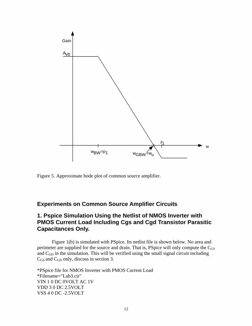
Figure 5. Approxim
xperiments on Common Source Amplifier Circuits
. Pspice Simulation Using the Netlist of NMOS Inverter with
his will be verified using the small signal circuit including
GS and CGD only, discuss in section 3.
DD 3 0 DC 2.5VOLT
wz1
Gain
AV0
wBW=p1 wGBW=wu
ate bode plot of common source amplifier.
E
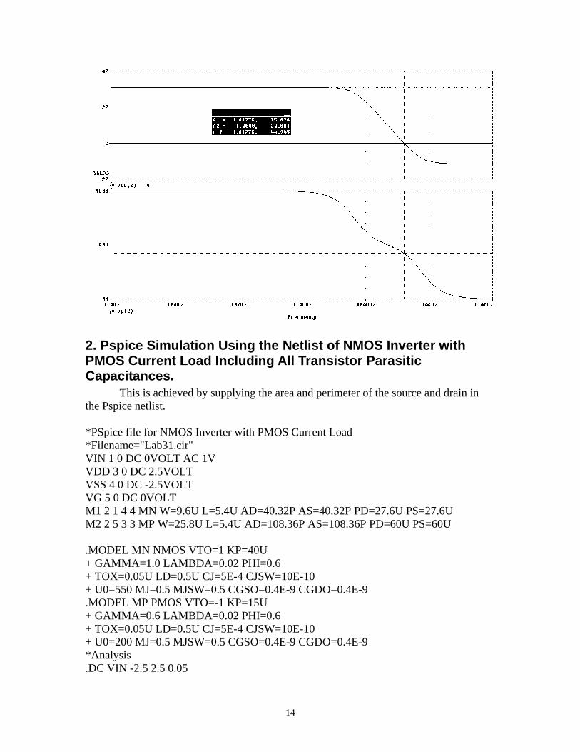
1PMOS Current Load Including Cgs and Cgd Transistor Parasitic Capacitances Only. Figure 1(b) is simulated with PSpice. Its netlist file is shown below. No area and perimeter are supplied for the source and drain. That is, PSpice will only compute the CGSand CGD in the simulation. TC *PSpice file for NMOS Inverter with PMOS Current Load *Filename="Lab3.cir" VIN 1 0 DC 0VOLT AC 1V VVSS 4 0 DC -2.5VOLT
12

VG 5 0 DC 0VOLT M1 2 1 4 4 MN W=9.6U L=5.4U
L=5.4U
VTO=1 KP=40U HI=0.6 CJSW=10E-10
U0=550 MJ=0.5 MJSW=0.5 CGSO=0.4E-9 CGDO=0.4E-9
ted parameters are:
o75.826PM
M218.44f 3-AA
GBWV
=
==
M2 2 5 3 3 MP W=25.8U .MODEL MN NMOS+ GAMMA=1.0 LAMBDA=0.02 P+ TOX=0.05U LD=0.5U CJ=5E-4 +.MODEL MP PMOS VTO=-1 KP=15U + GAMMA=0.6 LAMBDA=0.02 PHI=0.6 + TOX=0.05U LD=0.5U CJ=5E-4 CJSW=10E-10 + U0=200 MJ=0.5 MJSW=0.5 CGSO=0.4E-9 CGDO=0.4E-9 *Analysis .DC VIN -2.5 2.5 0.05 .TF V(2) VIN .AC DEC 100 1HZ 10GHZ .PROBE .END The extrac
G6127.1f db 0ABWV0V
==
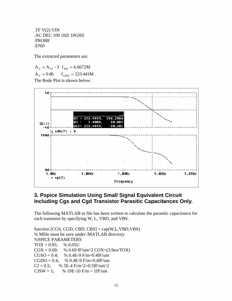
: The Bode Plot is shown below:
13
2. Pspice Simulation Using the Netlist of NMOS Inverter with PMOS Current Load Including All Transistor Parasitic Capacitances. This is achieved by supplying the area and perimeter of the source and drain in the Pspice netlist. *PSpice file for NMOS Inverter with PMOS Current Load *Filename="Lab31.cir" VIN 1 0 DC 0VOLT AC 1V VDD 3 0 DC 2.5VOLT VSS 4 0 DC -2.5VOLT VG 5 0 DC 0VOLT M1 2 1 4 4 MN W=9.6U L=5.4U AD=40.32P AS=40.32P PD=27.6U PS=27.6U M2 2 5 3 3 MP W=25.8U L=5.4U AD=108.36P AS=108.36P PD=60U PS=60U .MODEL MN NMOS VTO=1 KP=40U + GAMMA=1.0 LAMBDA=0.02 PHI=0.6 + TOX=0.05U LD=0.5U CJ=5E-4 CJSW=10E-10 + U0=550 MJ=0.5 MJSW=0.5 CGSO=0.4E-9 CGDO=0.4E-9 .MODEL MP PMOS VTO=-1 KP=15U + GAMMA=0.6 LAMBDA=0.02 PHI=0.6 + TOX=0.05U LD=0.5U CJ=5E-4 CJSW=10E-10 + U0=200 MJ=0.5 MJSW=0.5 CGSO=0.4E-9 CGDO=0.4E-9 *Analysis .DC VIN -2.5 2.5 0.05
14
.TF V(2) VIN
.AC DEC 100 1HZ 10GHZ
.PROBE
.END The extracted parameters are:
he Bode Plot is shown below: M441.223f db 0A
M6672.6f 3-AA
GBWV
BWV0V
====
T
3. Pspice Simulation Using Small Signal Equivalent Circuit nly.
he following MATLAB m file has been written to calculate the parasitic capacitance for
nction [CGS, CGD, CBD, CBS] = cap(W,L,VBD,VBS)
/um^2 COX=(3.9eo/TOX)
CJSW = 1; % 10E-10 F/m = 1fF/um
Including Cgs and Cgd Transistor Parasitic Capacitances O Teach transistor by specifying W, L, VBD, and VBS. fu% Mfile must be save under /MATLAB directory %SPICE PARAMETERS TOX = 0.05; % 0.05U COX = 0.69; % 0.69 fFCGSO = 0.4; % 0.4E-9 F/m=0.4fF/um CGDO = 0.4; % 0.4E-9 F/m=0.4fF/um CJ = 0.5; % 5E-4 F/m^2=0.5fF/um^2
15
LD = 0.5 % 0.5U MJ = 0.5; MJSW = 0.5; PHI=0.6; % 0.5 V
METERS END
u actual measurement from LAB3 layout * LEFF;
CGC;
N);
D/PHI)^MJ; VBD/PHI)^MJSW;
SW;
*W*LEFF; BSJ = CJ/(1 - VBS/PHI)^MJ;
S/PHI)^MJSW; W;
using the circuit for lab3.
cap (9.6, 5.4, -2.5, 0) GS = 23.2704 CGD = 3.8400 CBD = 21.0116 CBS = 61.8400
= cap (25.8, 5.4, -2.5, 0) GS = 62.5392 CGD = 10.3200 CBD = 50.2325 CBS = 152.0200
GSn = 23.2704 fF
lent circuit of NMOS inverter with PMOS CGS CGD are calculated
%SPICE PARALEFF=L-2*LD; LMIN = 4.2; % 7*(.6)=4.2; 4.5CGC = COX * WCGSOX = CGSO * W; CGDOX = CGDO * W; CGS = CGSOX + (2/3) *CGD = CGDOX; AD = W * LMIN; PD = 2*(W + LMIAS = W * LMIN; PS = 2*(W + LMIN); CBDJ = CJ/(1 - VBCBDJSW = CJSW/(1 -CBDO = AD*CBDJ + PD*CBDJCBD = CBDO; CBCJ = CJ; CBC = CBCJCCBSJSW = CJSW/(1 - VBCBSO = AS*CBSJ + PS*CBSJSCBS = CBSO + (2/3)* CBC; The following is a sample call For the NMOS transistor, [CGS, CGD, CBD, CBS] =C For the PMOS transistor, [CGS, CGD, CBD, CBS] C Co = CDBn + CDBp + CDGp = 21.0116 + 50.2325 + 10.32 = 81.5641 fFCCGDn = 3.8400 fF * Small signal equiva* Current load. Only* Filename=lab3eqn.cir"
16
Vin 1 0 AC 1V Rin 1 0 1E+20 Cgd 1 2 3.84fF Cgs 1 0 23.27fF
95u
Z 10GHZ
tracted parameters are:
G5493.1f db 0A GBWV ==
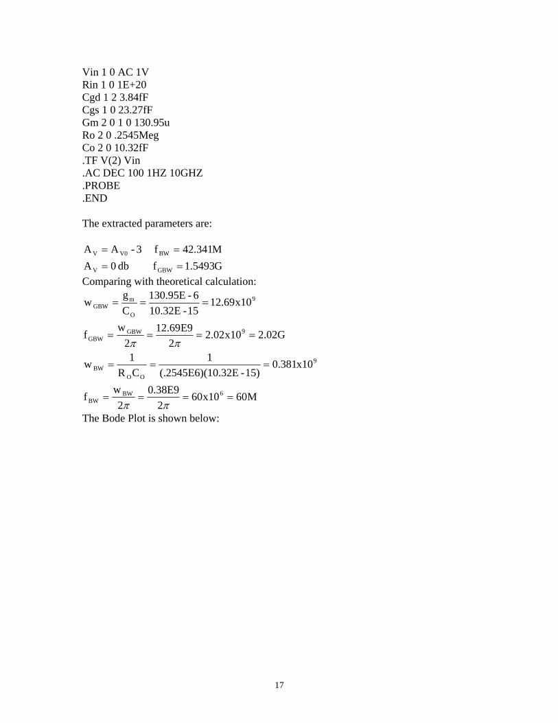
Gm 2 0 1 0 130.Ro 2 0 .2545MegCo 2 0 10.32fF .TF V(2) Vin .AC DEC 100 1H.PROBE .END The ex
M341.42f 3-AA BWV0V ==
Comparing with theoretical calculation:
M60x10602
E938.02
wf
x10381.015)-E6)(10.32E2545(.
1CR
1w
G02.2x1002.22
E969.122
wf
x1069.1215-E32.10
6-E95.130Cg
6BWBW
9
OOBW
9GBWGBW
9
O
mGBW
====
===
====
===
ππ
ππ
w
The Bode Plot is shown below:
17
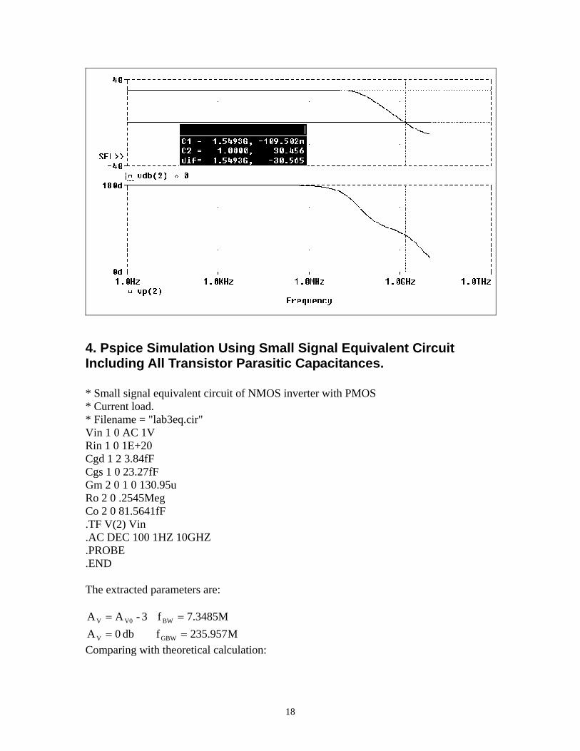
4. Pspice Simulation Using Small Signal Equivalent Circuit Including All Transistor Parasitic Capacitances. * Small signal equivalent circuit of NMOS inverter with PMOS * Current load. * Filename = "lab3eq.cir" Vin 1 0 AC 1V Rin 1 0 1E+20 Cgd 1 2 3.84fF Cgs 1 0 23.27fF Gm 2 0 1 0 130.95u Ro 2 0 .2545Meg Co 2 0 81.5641fF .TF V(2) Vin .AC DEC 100 1HZ 10GHZ .PROBE .END The extracted parameters are:
omparing with theoretical calculation: M957.235f db 0A
M3485.7f 3-AA
GBWV
BWV0V
====
C
18
M64.72
E9048.02
wf
G048.15)-E6)(81.56E2545(.
1CR
1w
M2562
E96054.12
wf
G6054.115-E5641.816-E95.130
Cgw
BWBW
OOBW
GBWGBW
O
mGBW
===
===
===
===
ππ
ππ
The Bode Plot is shown below:
Common Source Amplifier Design Procedure
Design Specif
mplifier with a gain of AV=50 and output impedance of o=1Meg.
//RR=
ssume RON=ROP, hence
=
ication
Design a common source aR OR OPON
A 2RRR OOPON == 2Meg
19
DSQP
OPDSQN
ON I1R
I1R
λλ===
Solving for IDSQ,
uA25E6)2)(02.0(
1R1
R1I =
OPPONN
===λλ
rom the gain equation the (W/L), can be obtained as follows:
DSQ
F
45
6)-6)(25E-E40(2E6)1/50(
I2K)/R(A
)/LW(
R)I/L(WK2RI2R-gA DSQNeffNNODSQNOmNV −=−== β 2
DSQN
2OV
NeffN
O
===
Using technology with λ=0.6u, the W, L are selected as follows:
NeffN
Neff
=+=+==== λ
3u5(0.6)5WN === λ
3.4u2(0.5u)u4.2LD2LL
u4.2)6.0(44L
The drawn length must be multiple of λ , hence LN=3.6u (=6λ), the nearest computed alue must be selected.
MOS are computed to achieve R=1, that is
v The W, L of the P β
u6.3LL
)13(7.8u select u;86)-E15(
6)(3u)-E40(K
WKW
LL since ; 1WK)/L(WKPeffNeff
PPPeffPPR ====β
WK)/L(WK
NP
P
NNP
NNNeffNN
==
==== λ
20
VG
VDD
Vo
Vi M1/MN1
M2/MP1
(2)
(1)
(4)
VSS
(5)
(3)
M3/MP2
VSS
(4)
Ibias
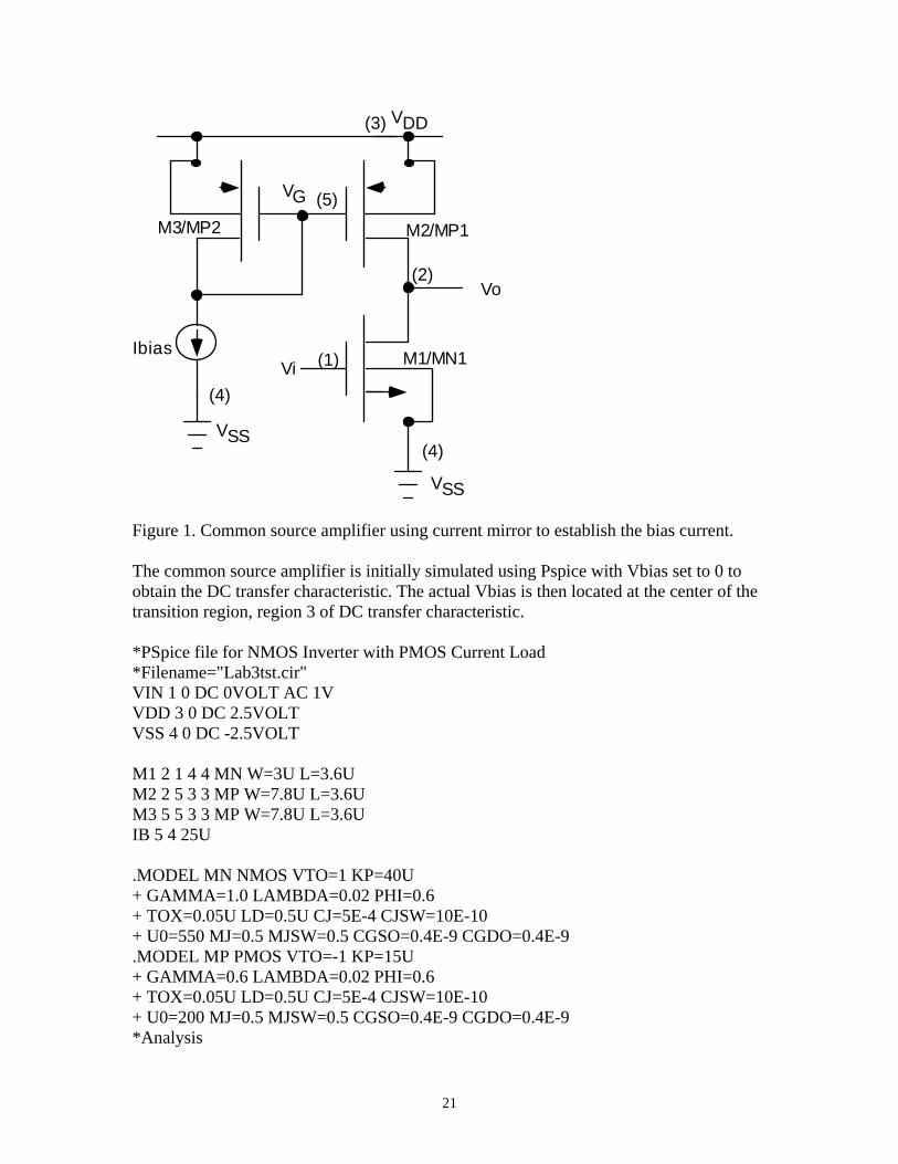
Figure 1. Common source amplifier using current mirror to establish the bias current. The common source amplifier is initially simulated using Pspice with Vbias set to 0 to obtain the DC transfer characteristic. The actual Vbias is then located at the center of the transition region, region 3 of DC transfer characteristic. *PSpice file for NMOS Inverter with PMOS Current Load *Filename="Lab3tst.cir" VIN 1 0 DC 0VOLT AC 1V VDD 3 0 DC 2.5VOLT VSS 4 0 DC -2.5VOLT M1 2 1 4 4 MN W=3U L=3.6U M2 2 5 3 3 MP W=7.8U L=3.6U M3 5 5 3 3 MP W=7.8U L=3.6U IB 5 4 25U .MODEL MN NMOS VTO=1 KP=40U + GAMMA=1.0 LAMBDA=0.02 PHI=0.6 + TOX=0.05U LD=0.5U CJ=5E-4 CJSW=10E-10 + U0=550 MJ=0.5 MJSW=0.5 CGSO=0.4E-9 CGDO=0.4E-9 .MODEL MP PMOS VTO=-1 KP=15U + GAMMA=0.6 LAMBDA=0.02 PHI=0.6 + TOX=0.05U LD=0.5U CJ=5E-4 CJSW=10E-10 + U0=200 MJ=0.5 MJSW=0.5 CGSO=0.4E-9 CGDO=0.4E-9 *Analysis
21
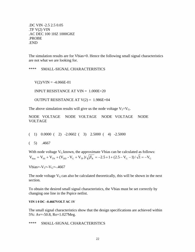
.DC VIN -2.5 2.5 0.05
.TF V(2) VIN
.AC DEC 100 1HZ 1000GHZ
.PROBE
.END The simulation results are for Vbias=0. Hence the following small signal characteristics are not what we are looking for. **** SMALL-SIGNAL CHARACTERISTICS V(2)/VIN = -4.066E-01 INPUT RESISTANCE AT VIN = 1.000E+20 OUTPUT RESISTANCE AT V(2) = 1.986E+04 The above simulation results will give us the node voltage V5=VG. NODE VOLTAGE NODE VOLTAGE NODE VOLTAGE NODE VOLTAGE ( 1) 0.0000 ( 2) -2.0602 ( 3) 2.5000 ( 4) -2.5000 ( 5) .4667 With node voltage VG known, the approximate Vbias can be calculated as follows:
GGRTPGDDTNSSbias V1/)1V5.2(15.2)/VV-(VVVV −=−−++−=+++= β Vbias=-V5=-VG=-.4667 The node voltage VG can also be calculated theoretically, this will be shown in the next section. To obtain the desired small signal characteristics, the Vbias must be set correctly by changing one line in the Pspice netlist. VIN 1 0 DC –0.4667VOLT AC 1V The small signal characteristics show that the design specifications are achieved within 5%: Av=-50.8, Ro=1.027Meg. **** SMALL-SIGNAL CHARACTERISTICS
22
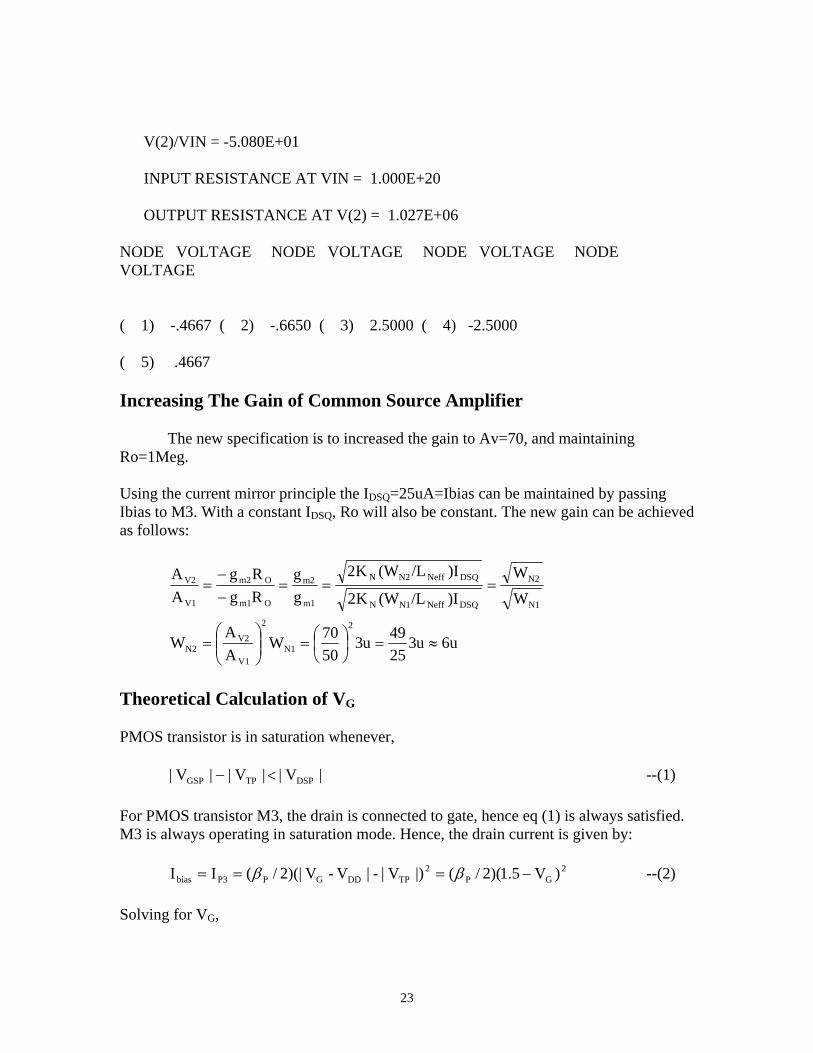
V(2)/VIN = -5.080E+01 INPUT RESISTANCE AT VIN = 1.000E+20 OUTPUT RESISTANCE AT V(2) = 1.027E+06 NODE VOLTAGE NODE VOLTAGE NODE VOLTAGE NODE VOLTAGE ( 1) -.4667 ( 2) -.6650 ( 3) 2.5000 ( 4) -2.5000 ( 5) .4667 Increasing The Gain of Common Source Amplifier The new specification is to increased the gain to Av=70, and maintaining Ro=1Meg. Using the current mirror principle the IDSQ=25uA=Ibias can be maintained by passing Ibias to M3. With a constant IDSQ, Ro will also be constant. The new gain can be achieved as follows:
6uu32549u3
5070W
AA
W
WW
)I/L(WK2
)I/L(WK2gg
RgRg
AA
2
N1
2
V1
V2N2
N1
N2
DSQNeffN1N
DSQNeffN2N
m1
m2
Om1
Om2
V1
V2
≈=⎟⎠⎞
⎜⎝⎛=⎟⎟
⎠
⎞⎜⎜⎝
⎛=
===−−
=
Theoretical Calculation of VG PMOS transistor is in saturation whenever, | --(1) V| |V||V| DSPTPGSP <− For PMOS transistor M3, the drain is connected to gate, hence eq (1) is always satisfied. M3 is always operating in saturation mode. Hence, the drain current is given by: --(2) 2
GP2
TPDDGPP3bias )V5.1)(2/(|)V|-|V-V)(|2/(II −=== ββ Solving for VG,
23
4459.0)6.2/8.7)(6E15(
6)-E25(25.1)/LW(K
I25.1
2I- 1.5V
PeffPP
bias
P
biasG =
−−=−==
β
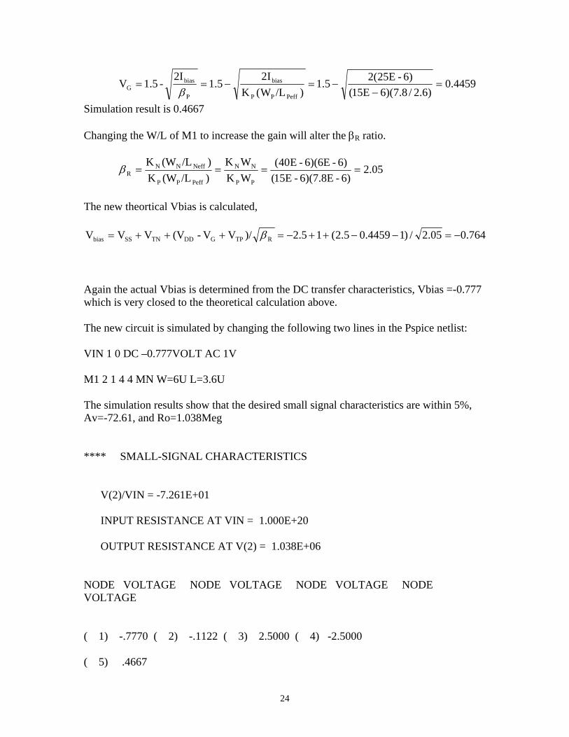
Simulation result is 0.4667 Changing the W/L of M1 to increase the gain will alter the βR ratio.
05.26)-6)(7.8E-E15(
6)-6)(6E-E40(WKWK
)/L(WK)/L(WK
PP
NN
PeffPP
NeffNNR ====β
The new theortical Vbias is calculated,
764.005.2/)14459.05.2(15.2)/VV-(VVVV RTPGDDTNSSbias −=−−++−=+++= β Again the actual Vbias is determined from the DC transfer characteristics, Vbias =-0.777 which is very closed to the theoretical calculation above. The new circuit is simulated by changing the following two lines in the Pspice netlist: VIN 1 0 DC –0.777VOLT AC 1V M1 2 1 4 4 MN W=6U L=3.6U The simulation results show that the desired small signal characteristics are within 5%, Av=-72.61, and Ro=1.038Meg **** SMALL-SIGNAL CHARACTERISTICS V(2)/VIN = -7.261E+01 INPUT RESISTANCE AT VIN = 1.000E+20 OUTPUT RESISTANCE AT V(2) = 1.038E+06 NODE VOLTAGE NODE VOLTAGE NODE VOLTAGE NODE VOLTAGE ( 1) -.7770 ( 2) -.1122 ( 3) 2.5000 ( 4) -2.5000 ( 5) .4667
24
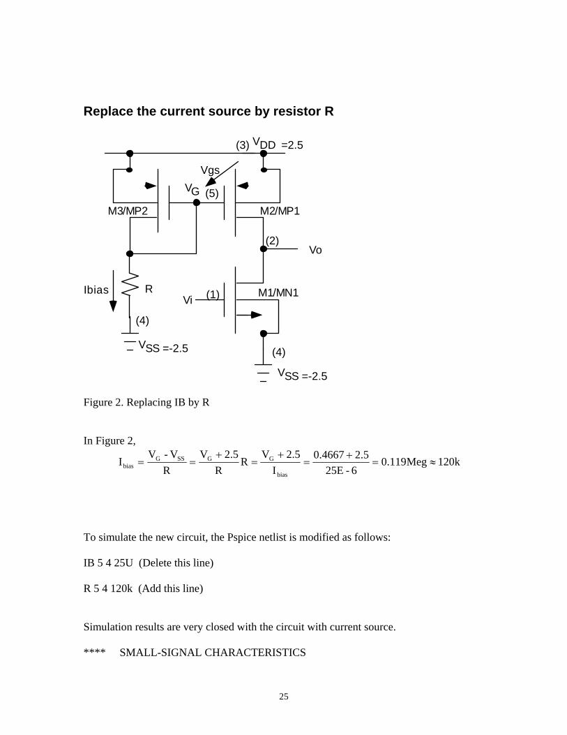
Replace the current source by resistor R
VG
VDD
Vo
Vi M1/MN1
M2/MP1
(2)
(1)
(4)
VSS
(5)
(3)
R
M3/MP2
VSS
(4)
=2.5
=-2.5
=-2.5
Vgs
Ibias
Figure 2. Replacing IB by R In Figure 2,
120kMeg119.06-E25
5.24667.0I
2.5VR
R2.5V
RV-V
Ibias
GGSSGbias ≈=
+=
+=
+==
To simulate the new circuit, the Pspice netlist is modified as follows: IB 5 4 25U (Delete this line) R 5 4 120k (Add this line) Simulation results are very closed with the circuit with current source. **** SMALL-SIGNAL CHARACTERISTICS
25
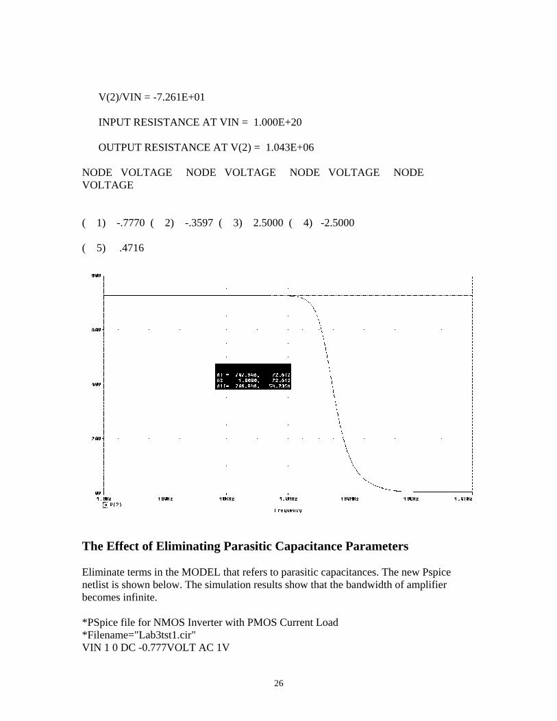
V(2)/VIN = -7.261E+01 INPUT RESISTANCE AT VIN = 1.000E+20 OUTPUT RESISTANCE AT V(2) = 1.043E+06 NODE VOLTAGE NODE VOLTAGE NODE VOLTAGE NODE VOLTAGE ( 1) -.7770 ( 2) -.3597 ( 3) 2.5000 ( 4) -2.5000 ( 5) .4716
The Effect of Eliminating Parasitic Capacitance Parameters Eliminate terms in the MODEL that refers to parasitic capacitances. The new Pspice netlist is shown below. The simulation results show that the bandwidth of amplifier becomes infinite. *PSpice file for NMOS Inverter with PMOS Current Load *Filename="Lab3tst1.cir" VIN 1 0 DC -0.777VOLT AC 1V
26
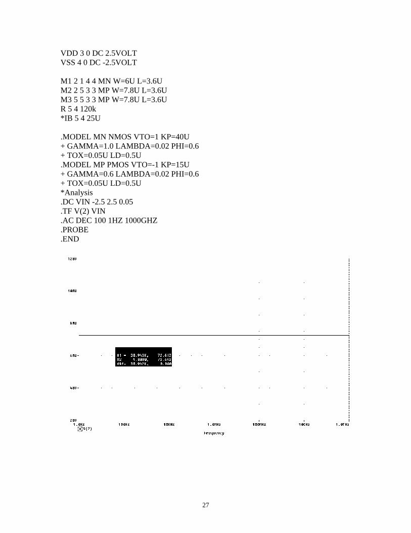
VDD 3 0 DC 2.5VOLT VSS 4 0 DC -2.5VOLT M1 2 1 4 4 MN W=6U L=3.6U M2 2 5 3 3 MP W=7.8U L=3.6U M3 5 5 3 3 MP W=7.8U L=3.6U R 5 4 120k *IB 5 4 25U .MODEL MN NMOS VTO=1 KP=40U + GAMMA=1.0 LAMBDA=0.02 PHI=0.6 + TOX=0.05U LD=0.5U .MODEL MP PMOS VTO=-1 KP=15U + GAMMA=0.6 LAMBDA=0.02 PHI=0.6 + TOX=0.05U LD=0.5U *Analysis .DC VIN -2.5 2.5 0.05 .TF V(2) VIN .AC DEC 100 1HZ 1000GHZ .PROBE .END
27