Embed Size (px)
Citation preview
1
Common myths, fallacies and misconceptions in Electromagnetic Compatibility and their correction.
D. A. Weston EMC Consulting Inc 15-3-2013
1) First topic an introduction
These are some of the commonly held beliefs about EMC which are either a mistake in reasoning, untrue,
only partially true (i.e. with many exceptions), without foundation, or based on misunderstanding.
EMC is indeed a complex issue in which all aspects of an EMI or EMC engineering situation must be
considered in order to arrive at the correct solution. The goal of this article is to help clarify some of these
situations.
Over a period of 32 years of EMC experience, and particularly during the presentation of seminars, these
are the myths and fallacies which I hear over and over again. This article is intended primarily for the
practicing electronic engineer or technician, who is not a specialist in the field of EMC/EMI or someone
starting out in EMC. It is presented in the hope that the explanations and clarifications may be of practical
use to the reader.
EMC/EMI is black magic.
Based on my experience, this is the most common comment made about EMC.
We often use the term magic when describing an unexpected or unusual result.
The term magic is used to describe astonishing results as at a magic show, when sound engineering is
often the basis of the magic trick. This may also be applied to some aspects of EMC.
Often the results of an EMI test, after inclusion of EMI mitigation or EMC engineering components, is
contrary to what is expected, and sometimes counter intuitive.
For example shielding against magnetic fields using thin materials with a relative permeability of 1 seems
like magic but has a simple explanation as described in references 1, 3, 4, and 5.
The major reason EMC is seen as magic is a lack of understanding of the underlying principles. Also the
coupling mechanism in an EMI problem may not have been identified or a number of coupling mechanisms
apply. Often the paths that RF currents take are not always obvious and parasitic components in a circuit
have been ignored.
Often many sources of emissions exist and when one has been minimized a second predominates. This
often means that a fix is less effective than expected.
Minor changes in PCB layout, component type or even make, lead length, location, and mechanical
assembly can lead to dramatic RF changes.
2) Cable shields must be connected to ground at one end only.
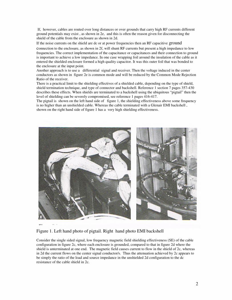
When a shielded cable is connected between two or more pieces of equipment contained in conductive
enclosures the shield should be thought of as an extension of the enclosures as shown in 2a. Therefore the
most effective grounding is as shown in 2a or 2b, where one or both enclosures are isolated from chassis.
This is often impractical and for safety and grounding philosophy reasons the enclosures are often
grounded at both ends as shown in 2c.
The common mistake is to assume that one end of the shield should be isolated from the enclosure as
shown in 2d and not the enclosure from ground. This results in only E field shielding, limited shielding of
plane waves when the cable is many wavelengths long, and no appreciable magnetic field shielding.
The most common reason given is to avoid ground loops. However other techniques are available and a
well thought out grounding philosophy, backed up by a power and grounding diagram , should be used.
High power and RF current should be routed on return conductors which are isolated from chassis at one
end and do not use the shield as a return path.
2
If, however, cables are routed over long distances or over grounds that carry high RF currents different
ground potentials may exist , as shown in 2e, and this is often the reason given for disconnecting the
shield of the cable from the enclosure as shown in 2d.
If the noise currents on the shield are dc or at power frequencies then an RF capacitive ground
connection to the enclosure, as shown in 2f, will shunt RF currents but present a high impedance to low
frequencies. The correct implementation of the capacitance or capacitances and their connection to ground
is important to achieve a low impedance. In one case wrapping foil around the insulation of the cable as it
entered the shielded enclosure formed a high quality capacitor. It was this outer foil that was bonded to
the enclosure at the input point.
Another approach is to use a differential signal and receiver. Then the voltage induced in the center
conductors as shown in figure 2e is common mode and will be reduced by the Common Mode Rejection
Ratio of the receiver.
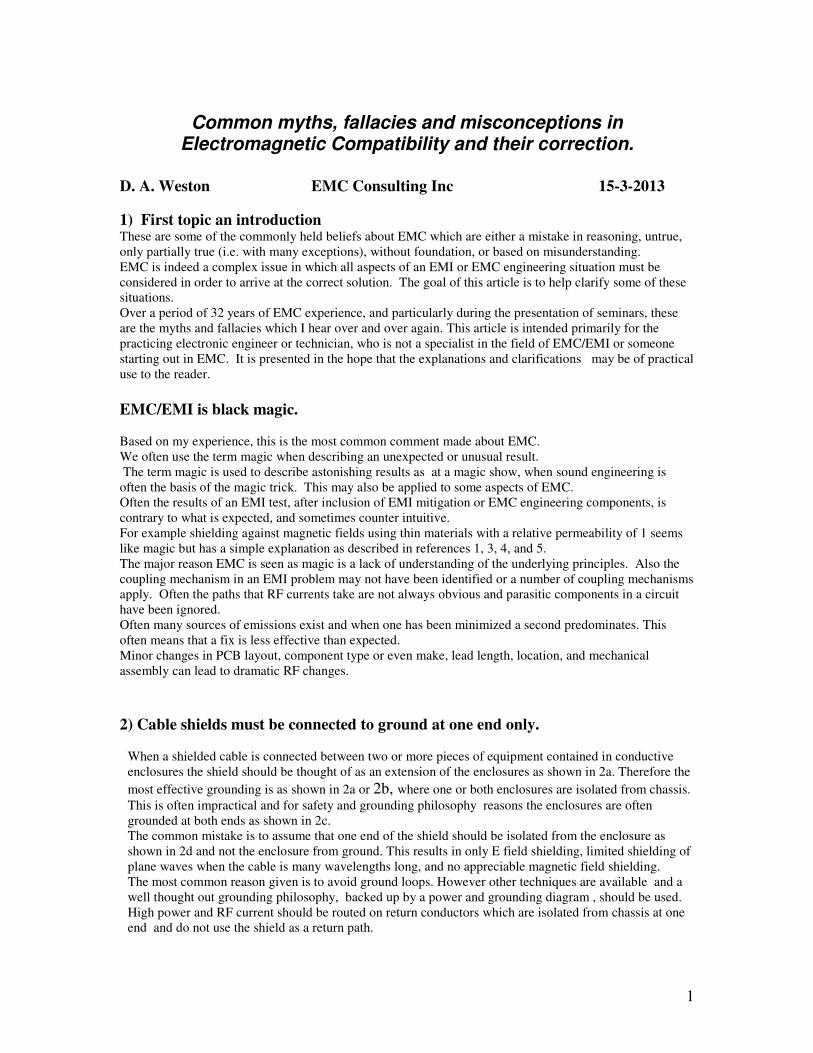
There is a practical limit to the shielding effectives of a shielded cable, depending on the type of shield,
shield termination technique, and type of connector and backshell. Reference 1 section 7 pages 357-430
describes these effects. When shields are terminated to a backshell using the ubiquitous “pigtail” then the
level of shielding can be severely compromised, see reference 1 pages 416-417.
The pigtail is shown on the left hand side of figure 1, the shielding effectiveness above some frequency
is no higher than an unshielded cable. Whereas the cable terminated with a Glenair EMI backshell ,
shown on the right hand side of figure 1 has a very high shielding effectiveness.
Figure 1. Left hand photo of pigtail. Right hand photo EMI backshell
Consider the single sided signal, low frequency magnetic field shielding effectiveness (SE) of the cable
configuration in figure 2c, where each enclosure is grounded, compared to that in figure 2d where the
shield is unterminated at one end. The magnetic field causes current to flow in the shield of 2c, whereas
in 2d the current flows on the center signal conductor/s. Thus the attenuation achieved by 2c appears to
be simply the ratio of the load and source impedance in the unshielded 2d configuration to the dc
resistance of the cable shield in 2c.
3
However the current induced in the cable shield by the incident magnetic field is much higher in figure 2c
than in the center conductor signal wire in figure 2d. This means that up to about 1kHz the shielded cable
shielding effectiveness is approximately zero. Above 1kHz the current induced into the shield of the cable
decreases and the voltage drop in the shield is a function of its transfer impedance. Transfer impedance is
defined as the voltage developed between the inside of the shield and the center conductor/s divided by
the shield current.
For a typical shielded cable/conduit the magnetic field SE is 16dB (numeric 6.3) at 100kHz and 36dB (numeric 63)at 1MHz. Reference 2 describes this further
2a
2bground
ground
ground
2c
2d
ground
2eground
2f
V
Figures 2a to 2f
4
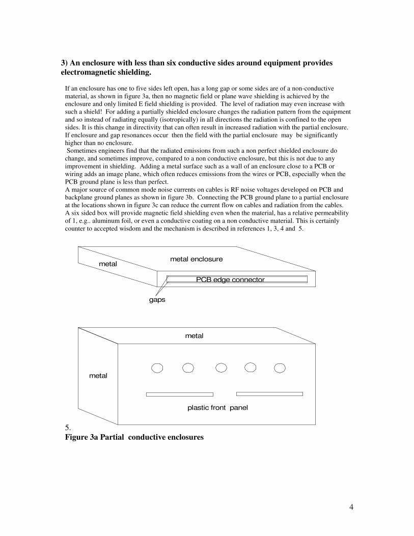
3) An enclosure with less than six conductive sides around equipment provides
electromagnetic shielding.
If an enclosure has one to five sides left open, has a long gap or some sides are of a non-conductive
material, as shown in figure 3a, then no magnetic field or plane wave shielding is achieved by the
enclosure and only limited E field shielding is provided. The level of radiation may even increase with
such a shield! For adding a partially shielded enclosure changes the radiation pattern from the equipment
and so instead of radiating equally (isotropically) in all directions the radiation is confined to the open
sides. It is this change in directivity that can often result in increased radiation with the partial enclosure.
If enclosure and gap resonances occur then the field with the partial enclosure may be significantly
higher than no enclosure.
Sometimes engineers find that the radiated emissions from such a non perfect shielded enclosure do
change, and sometimes improve, compared to a non conductive enclosure, but this is not due to any
improvement in shielding. Adding a metal surface such as a wall of an enclosure close to a PCB or
wiring adds an image plane, which often reduces emissions from the wires or PCB, especially when the
PCB ground plane is less than perfect.
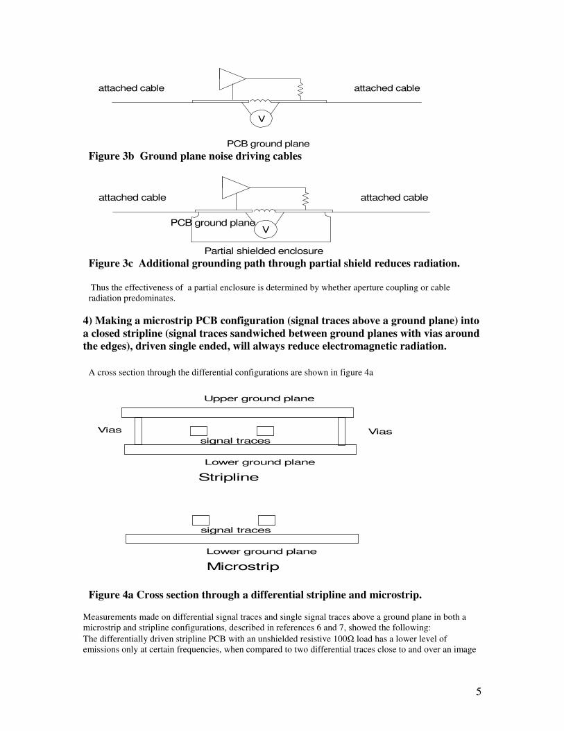
A major source of common mode noise currents on cables is RF noise voltages developed on PCB and
backplane ground planes as shown in figure 3b. Connecting the PCB ground plane to a partial enclosure
at the locations shown in figure 3c can reduce the current flow on cables and radiation from the cables.
A six sided box will provide magnetic field shielding even when the material, has a relative permeability
of 1, e.g.. aluminum foil, or even a conductive coating on a non conductive material. This is certainly
counter to accepted wisdom and the mechanism is described in references 1, 3, 4 and 5.
5.
PCB edge connector
gaps
metal enclosure
metal
metal
plastic front panel
metal
Figure 3a Partial conductive enclosures
5
PCB ground plane
attached cable attached cable
V
Figure 3b Ground plane noise driving cables
Partial shielded enclosure
PCB ground plane
attached cable attached cable
V
Figure 3c Additional grounding path through partial shield reduces radiation. Thus the effectiveness of a partial enclosure is determined by whether aperture coupling or cable
radiation predominates.
4) Making a microstrip PCB configuration (signal traces above a ground plane) into
a closed stripline (signal traces sandwiched between ground planes with vias around
the edges), driven single ended, will always reduce electromagnetic radiation.
A cross section through the differential configurations are shown in figure 4a
Stripline
Lower ground plane
Upper ground plane
ViasVias
signal traces
Lower ground plane
signal traces
Microstrip
Figure 4a Cross section through a differential stripline and microstrip.
Measurements made on differential signal traces and single signal traces above a ground plane in both a
microstrip and stripline configurations, described in references 6 and 7, showed the following:
The differentially driven stripline PCB with an unshielded resistive 100Ω load has a lower level of
emissions only at certain frequencies, when compared to two differential traces close to and over an image
6
plane (the lower ground plane). At high frequencies the level of emissions is similar. This configuration
with unshielded components more accurately represents the real world. Other comparisons in the same
reports between differential stripline and differential traces with image plane and unshielded loads on
different PCB configurations clearly show that the stripline radiates at a lower level.
In the stripline PCB configuration that has a fully shielded load and connector, the emissions are extremely
low. As the emissions from the stripline are so low, emissions from connectors, short lengths of unshielded
traces outside of the stripline and ICs will predominate and the distance between the vias tacking the upper
and lower ground planes has little effect on the level of radiation as the PCB is no longer the prime source.
Measurements were also made with only one trace used as the signal and the signal return connected to the
ground plane in either the stripline or microstrip PCBs. We refer to this as a single sided measurement. The
measurements showed that the single sided stripline with unshielded load is on average only 6dB lower
than the single sided microstrip over the 50MHz to 1100MHz frequency range and from 1100MHz to
1350MHz it is up to 10dB higher!
When the major source of radiation is the PCB and not components observation of numerous PCB layouts
has shown that the radiation from a PCB with full upper and lower ground planes tied together with a
number of vias is invariably lower than a PCB with a single ground plane. Also a PCB with an overall
ground plane and an incomplete second ground plane with small islands, is only more effective than the
PCB with a single ground plane when the islands are connected to the overall ground plane using a number
of vias.
It is very important when signals transit from the far side of a PCB ground plane to the far side of a second
PCB ground plane to ensure that vias connect the ground planes together as shown with a VCC plane in
figure 3c. The reasons for this are many and are included in references 6 and 7.
Layer 1 Ground plane
Layer 2 Signal
Layer 3 VCC
Layer 4 Signal
Layer 5 Ground Plane
Ground vias surrounding signal via
Transition
Figure 3.c Vias connecting the ground planes together close to a signal transition.
A solid ground plane on a PCB or backplane used as a current return path will have
an impedance in the µOhms
When a ground plane is quoted as having an impedance in the µ Ohms this refers to its dc intrinsic or metal
impedance. This is the impedance seen by an incident electromagnetic wave. However when the ground
plane forms a path for RF currents, due to its inductance, the impedance will be much higher. For example
from reference 1, the impedance of a 12.6cm x 10cm copper 1oz ground is 0.64Ω at 2MHz when the signal
conductor is 1cm above the ground plane and 0.045Ω when the signal conductor is 1mm above it.
7
5) If equipment is contained in a six sided conductive box (enclosure) it will meet
all EMI requirements.
This common fallacy ignores the radiation from cables entering and exiting the enclosure and the weak
link in an enclosure, namely seams and apertures.
When PCBs are contained in an enclosure the fields generated by the PCBs set up RF currents on the
inside walls of the enclosure. The fields also couple back to the PCB and set up common mode RF
currents in the PCB ground and traces. Connecting signal returns multipoint to the chassis also injects
noise currents into the chassis.
Often the shield of a cable is brought through the enclosure and terminated to the inside of the enclosure.
The RF current flowing on this surface then flow out on the shield. When the shield is terminated on the
outside of the enclosure radiation from the shield commonly reduces significantly.
Any unshielded cable, or cable with a shield terminated on the noisy PCB ground, which exits the
enclosure without filtering may have cable currents higher than with an unshielded enclosure. The reason
is that the radiation from the PCB sets up currents in the inside of the enclosure which in turn generates
fields impinging on the PCB. At the least the frequency of maximum radiation may change with the
shielded enclosure versus unshielded.
The shield should be terminated around 360 degrees to an EMI backshell , preferably solid metal and not
conductively coated plastic as shown in the right hand side of figure 1. To meet low level radiated
emission limits with a braided shielded cable signal return currents on the shield should be avoided
where possible or limited in magnitude. Common mode currents on the inside of the shield can be
reduced using the techniques shown in figures 10b, 10c and 10d.
In many enclosures the fasteners are too far apart. Often in a thick milled enclosure gaps may appear
between fasteners when the sides of the enclosure are not of the same height, see reference 1 section 6.4
page 304. For magnetic fields the size of the gap between two mating surfaces is not important. It is the
length of the gap, the dc resistance and the frequency dependent contact resistance which limits the
enclosures shielding effectiveness, reference 1 section 6.4.3 page 316 and reference 8.
6) A power line filter, which is effective when tested alone, will remain effective
when mounted on a PCB which contains noise sources such as a switching power
supply or digital components.
A power line filter which is unshielded with unshielded input power lines can have RF coupled to both the
components and the input connections to the filter. This is most likely when the filter components are
mounted on a PCB containing noise sources, such as switching power supplies or digital logic. The
problem may be exacerbated when the input power is routed down a backplane, which is also used for
digital data.
If the noisy power line is run close to the filtered power line then the resultant cross talk can either reduce
the filter attenuation or even negate it completely.
Very often an effective filter capable of meeting all EMI requirements will fail conducted emission tests
when unshielded and PCB mounted. If the input power lines to the equipment enclosure are unshielded a
PCB mounted filter may also result in a failure in radiated emission measurements.
Ideally the power line filter will be shielded and mounted on the equipment enclosure wall with the input
power connector mounted to the filter enclosure. All of the power line filters in figure 2 are shielded but
may still suffer coupling between the input and output wiring. The filter in the center of the photo, with the
connector, is mounted inside the enclosure with the connector on the outside and this configuration shows
minimal coupling. If this is not feasible then the shielded filter should be mounted as close to the input
power connector with shielded wires used to connect between the connector and the filter. A compromise,
which may work, is to have the low frequency filtering components mounted on the PCB and additional
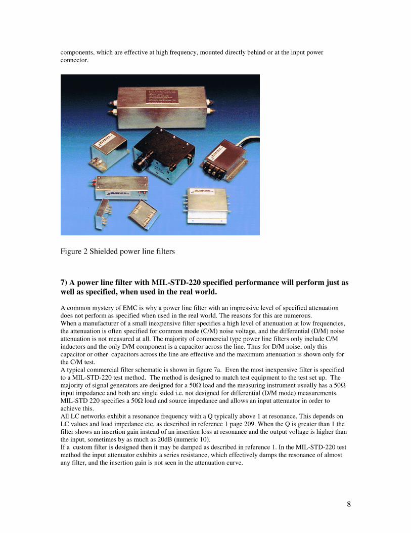
8
components, which are effective at high frequency, mounted directly behind or at the input power
connector.
Figure 2 Shielded power line filters
7) A power line filter with MIL-STD-220 specified performance will perform just as
well as specified, when used in the real world.
A common mystery of EMC is why a power line filter with an impressive level of specified attenuation
does not perform as specified when used in the real world. The reasons for this are numerous.
When a manufacturer of a small inexpensive filter specifies a high level of attenuation at low frequencies,
the attenuation is often specified for common mode (C/M) noise voltage, and the differential (D/M) noise
attenuation is not measured at all. The majority of commercial type power line filters only include C/M
inductors and the only D/M component is a capacitor across the line. Thus for D/M noise, only this
capacitor or other capacitors across the line are effective and the maximum attenuation is shown only for
the C/M test.
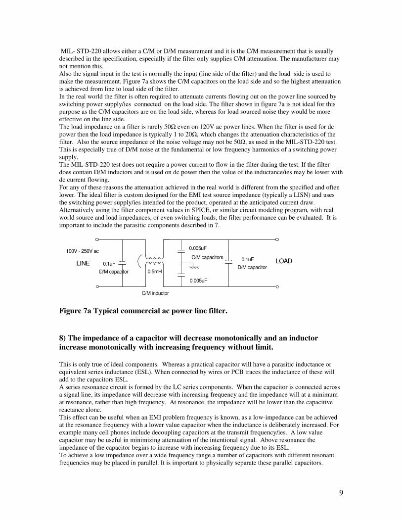
A typical commercial filter schematic is shown in figure 7a. Even the most inexpensive filter is specified
to a MIL-STD-220 test method. The method is designed to match test equipment to the test set up. The
majority of signal generators are designed for a 50Ω load and the measuring instrument usually has a 50Ω
input impedance and both are single sided i.e. not designed for differential (D/M mode) measurements.
MIL-STD 220 specifies a 50Ω load and source impedance and allows an input attenuator in order to
achieve this.
All LC networks exhibit a resonance frequency with a Q typically above 1 at resonance. This depends on
LC values and load impedance etc, as described in reference 1 page 209. When the Q is greater than 1 the
filter shows an insertion gain instead of an insertion loss at resonance and the output voltage is higher than
the input, sometimes by as much as 20dB (numeric 10).
If a custom filter is designed then it may be damped as described in reference 1. In the MIL-STD-220 test
method the input attenuator exhibits a series resistance, which effectively damps the resonance of almost
any filter, and the insertion gain is not seen in the attenuation curve.
9
MIL- STD-220 allows either a C/M or D/M measurement and it is the C/M measurement that is usually
described in the specification, especially if the filter only supplies C/M attenuation. The manufacturer may
not mention this.
Also the signal input in the test is normally the input (line side of the filter) and the load side is used to
make the measurement. Figure 7a shows the C/M capacitors on the load side and so the highest attenuation
is achieved from line to load side of the filter.
In the real world the filter is often required to attenuate currents flowing out on the power line sourced by
switching power supply/ies connected on the load side. The filter shown in figure 7a is not ideal for this
purpose as the C/M capacitors are on the load side, whereas for load sourced noise they would be more
effective on the line side.
The load impedance on a filter is rarely 50Ω even on 120V ac power lines. When the filter is used for dc
power then the load impedance is typically 1 to 20Ω, which changes the attenuation characteristics of the
filter. Also the source impedance of the noise voltage may not be 50Ω, as used in the MIL-STD-220 test.
This is especially true of D/M noise at the fundamental or low frequency harmonics of a switching power
supply.
The MIL-STD-220 test does not require a power current to flow in the filter during the test. If the filter
does contain D/M inductors and is used on dc power then the value of the inductance/ies may be lower with
dc current flowing.
For any of these reasons the attenuation achieved in the real world is different from the specified and often
lower. The ideal filter is custom designed for the EMI test source impedance (typically a LISN) and uses
the switching power supply/ies intended for the product, operated at the anticipated current draw.
Alternatively using the filter component values in SPICE, or similar circuit modeling program, with real
world source and load impedances, or even switching loads, the filter performance can be evaluated. It is
important to include the parasitic components described in 7.
0.5mH
0.1uF
C/M inductor
D/M capacitor
C/M capacitors
0.005uF
0.005uF
0.1uF
D/M capacitor
100V - 250V ac
LINE LOAD
Figure 7a Typical commercial ac power line filter.
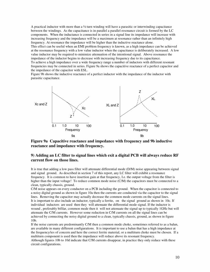
8) The impedance of a capacitor will decrease monotonically and an inductor
increase monotonically with increasing frequency without limit.
This is only true of ideal components. Whereas a practical capacitor will have a parasitic inductance or
equivalent series inductance (ESL). When connected by wires or PCB traces the inductance of these will
add to the capacitors ESL.
A series resonance circuit is formed by the LC series components. When the capacitor is connected across
a signal line, its impedance will decrease with increasing frequency and the impedance will at a minimum
at resonance, rather than high frequency. At resonance, the impedance will be lower than the capacitive
reactance alone.
This effect can be useful when an EMI problem frequency is known, as a low-impedance can be achieved
at the resonance frequency with a lower value capacitor when the inductance is deliberately increased. For
example many cell phones include decoupling capacitors at the transmit frequency/ies. A low value
capacitor may be useful in minimizing attenuation of the intentional signal. Above resonance the
impedance of the capacitor begins to increase with increasing frequency due to its ESL.
To achieve a low impedance over a wide frequency range a number of capacitors with different resonant
frequencies may be placed in parallel. It is important to physically separate these parallel capacitors.
10
A practical inductor with more than a ½ turn winding will have a parasitic or interwinding capacitance
between the windings. As the capacitance is in parallel a parallel resonance circuit is formed by the LC
components. When the inductance is connected in series in a signal line its impedance will increase with
increasing frequency and the impedance will be a maximum at resonance rather than an infinitely high
frequency. At resonance the impedance will be higher than the inductive reactance alone.
This effect can be useful when an EMI problem frequency is known, as a high impedance can be achieved
at the resonance frequency with a low value inductor when the capacitance is deliberately increased. A low
value inductor may be required to minimize attenuation of the intentional signal. Above resonance the
impedance of the inductor begins to decrease with increasing frequency due to its capacitance.
To achieve a high impedance over a wide frequency range a number of inductors with different resonant
frequencies may be connected in series. Figure 9a shows the capacitive reactance of a perfect capacitor and
the impedance of the capacitor with ESL.
Figure 9b shows the inductive reactance of a perfect inductor with the impedance of the inductor with
parasitic capacitance.
Xc and Z
Frequency
0.1 1.0 10 100Frequency
0.1 1.0 10 100
Z
XcXL and Z
Z
XL
9a 9b Figure 9a Capacitive reactance and impedance with frequency and 9b inductive
reactance and impedance with frequency.
9) Adding an LC filter to signal lines which exit a digital PCB will always reduce RF
current flow on those lines.
It is true that adding a low pass filter will attenuate differential mode (D/M) noise appearing between signal
and signal ground. As described in section 7 of this report, any LC filter will exhibit a resonance
frequency. It is common to have insertion gain at that frequency, I.e. the output voltage from the filter is
higher than the input voltage! To reduce common mode noise (C/M) the capacitors must be connected to a
clean, typically chassis, ground.
C/M noise appears on every conductor on a PCB including the ground. When the capacitor is connected to
a noisy digital ground as shown in figure 10a then the currents are conducted via the capacitor to the signal
lines. Removing the capacitor may actually decrease the common mode currents on the signal lines.
It is important to also include an inductor, typically a ferrite, on the signal ground as shown in 10c. If
individual inductors are used then they will attenuate the differential mode signal. If the inductor is
wound , preferably bifilar, common mode then it will not attenuate the signal up to typically 1GHz but will
attenuate the C/M currents. However some reduction in C/M currents on all the signal lines can be
achieved by connecting the noisy digital ground to a clean, typically chassis, ground, as shown in figure
10b.
If the noise currents are predominantly C/M then a common mode choke, sometimes referred to as a balun,
are available in many different configurations. It is important to use a balun that has a high impedance at
the frequency/ies of concern and here the correct ferrite material, or a multiturn choke must be chosen. If a
multiturn component is used then the impedance will reduce above its resonant frequency.
Although figures 10b to 10d indicate that C/M currents disappear, in practice they only reduce with these
circuit configurations.
11
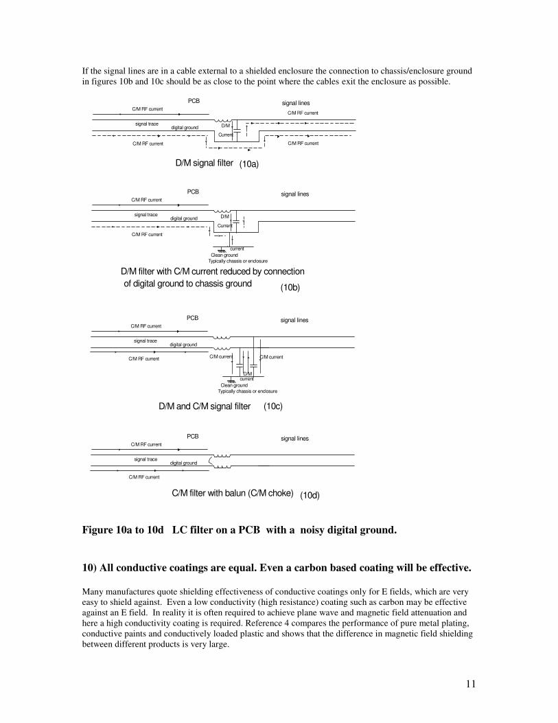
If the signal lines are in a cable external to a shielded enclosure the connection to chassis/enclosure ground
in figures 10b and 10c should be as close to the point where the cables exit the enclosure as possible.
PCB
digital groundsignal trace
signal lines
C/M RF currentC/M RF current
C/M RF currentC/M RF current
D/M signal filter
PCB
digital groundsignal trace
signal lines
C/M RF current
C/M RF current
D/M
Current
Clean ground
Typically chassis or enclosure
D/M and C/M signal filter
PCB
digital groundsignal trace
signal lines
C/M RF current
C/M RF current
C/M filter with balun (C/M choke)
C/M currentC/M current
D/M
current
(10a)
(10c)
(10d)
PCB
digital groundsignal trace
signal lines
C/M RF current
C/M RF current
D/M
Current
(10b)
Clean ground
Typically chassis or enclosure
current
D/M filter with C/M current reduced by connection
of digital ground to chassis ground
Figure 10a to 10d LC filter on a PCB with a noisy digital ground.
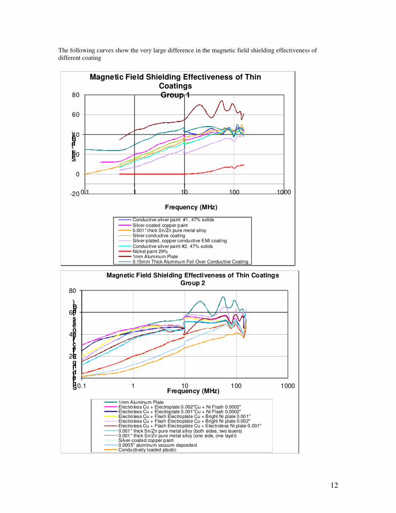
10) All conductive coatings are equal. Even a carbon based coating will be effective.
Many manufactures quote shielding effectiveness of conductive coatings only for E fields, which are very
easy to shield against. Even a low conductivity (high resistance) coating such as carbon may be effective
against an E field. In reality it is often required to achieve plane wave and magnetic field attenuation and
here a high conductivity coating is required. Reference 4 compares the performance of pure metal plating,
conductive paints and conductively loaded plastic and shows that the difference in magnetic field shielding
between different products is very large.
12
The following curves show the very large difference in the magnetic field shielding effectiveness of
different coating
-20
0
20
40
60
80
0.1 1 10 100 1000
S.E. (dB)
Frequency (MHz)
Magnetic Field Shielding Effectiveness of Thin CoatingsGroup 1
Conductive silver paint #1, 47% solidsSilver-coated copper paint0.001" thick Sn/Zn pure metal alloySilver conductive coatingSilver-plated, copper conductive EMI coatingConductive silver paint #2, 47% solidsNickel paint 29%1mm Aluminum Plate0.15mm Thick Aluminum Foil Over Conductive Coating
0
20
40
60
80
0.1 1 10 100 1000Shielding Effectiveness (dB)
Frequency (MHz)
Magnetic Field Shielding Effectiveness of Thin CoatingsGroup 2
1mm Aluminum PlateElectroless Cu + Electroplate 0.002"Cu + Ni Flash 0.0002"Electroless Cu + Electroplate 0.001"Cu + Ni Flash 0.0002"Electroless Cu + Flash Electroplate Cu + Bright Ni plate 0.001"Electroless Cu + Flash Electroplate Cu + Bright Ni plate 0.002"Electroless Cu + Flash Electroplate Cu + Electroless Ni plate 0.001"0.001" thick Sn/Zn pure metal alloy (both sides, two layers)0.001" thick Sn/Zn pure metal alloy (one side, one layer)Silver-coated copper paint0.0005" aluminum vacuum depositedConductively loaded plastic
13
11) Adding a ferrite toroid or bead (balun) to a cable will always reduce any RF current flowing on
the cable.
If no current probe is available adding a ferrite on a cable is often used as a diagnostic tool to determine if
RF current is flowing as well in EMI mitigation to reduce the current.
If a cable is electrically long ( greater than ½ wavelength) then the current on the cable is maximum at
some location and zero at another. The high current location has a low impedance and the low current a
high impedance. If a ferrite balun is placed on the low impedance section then any RF current within the
frequency range of the ferrite will be reduced due to the impedance of the ferrite. However when placed at
a high impedance section the current will not be reduced. Therefore move a ferrite up and down the cable
to ensure that a low impedance section is found.
If the RF frequency is 50 MHz to 250MHz then a #28 material ferrite presents the highest impedance. If
between 8MHz and 50MHz a #33 and for 200MHz and above a #25 Material.
Some ferrites are effective in the 1-2GHz range. For frequencies below 5MHz and especially around
100kHz a high permeability material such as a W material, which has a relative permeability of 100,000
may be useful.
A ferrite on a cable or wire also acts as an effective receiving antenna. If a ferrite is located on a PCB close
to a source of high level RF , such as a clock oscillator, switching power supply or digital Ics the fields
generated by these devices may couple to the ferrite and inject current into the cable and wire and then
adding the ferrite is counterproductive.
If C/M RF current flows on a number of wires or cables in close proximity to each other then baluns are
required either on each conductor, including signal and power grounds or overall. A common mistake is to
put the dc power through one balun and the return through another. The resultant D/M current can saturate
the ferrite. When signal and returns are placed through the same aperture in the ferrite the balun will not
attenuate D/M signals up to 1GHz. However when the signal is routed through one hole in a two hole balun
and the signal return through another attenuation of the signal is seen at much lower frequencies.
REFERENCES
1) Electromagnetic Compatibility: Principles and Applications. D. A. Weston.
Published by Marcel Dekker. 2001.
2) 150Hz to 1MHz magnetic field coupling to a typical shielded cable above a
ground plane configuration. Report on www.emcconsultinginc.com
3) An explanation of the “magic” low frequency magnetic field shielding
effectiveness of conductive foil with a permeability of 1. Report on
www.emcconsultinginc.com
4) Comparative magnetic field shielding effectiveness of thin conductive coatings.
Report on www.emcconsultinginc.com
5) Electromagnetic Compatibility Handbook . K.L. Kaiser CRC Press 2005. Section
23.1 page 23.1.
6) PCB Electromagnetic radiation due to high speed logic from different layouts.
Report on www.emcconsultinginc.com.
7) How much better is a practical stripline PCB layout than a microstrip?
Paper presented at the Asia Pacific EMC Symposium May 2008
8) Seams as the weak link in E field and plane wave shielding effectiveness . Report
on www.emcconsultinginc.com.