Embed Size (px)
DESCRIPTION
coils on pcb
Citation preview

Nat.Lab. Technical Note 2001/218
Date of issue: 06/01
Technical Note
Coils on PCB
Michel de Clercq and Tarik Saric(Hogeschool Eindhoven)
Company Restricted Koninklijke Philips Electronics N.V. 2001
ii Koninklijke Philips Electronics N.V. 2001
2001/218 Company Restricted
Authors’ address data: Currently working outside Philips.
Koninklijke Philips Electronics N.V. 2001All rights are reserved. Reproduction in whole or in part is
prohibited without the written consent of the copyright owner.
Company Restricted 2001/218
Koninklijke Philips Electronics N.V. 2001 iii
Technical Note: 2001/218
Title: Coils on PCB
Author(s): Michel de Clercq and Tarik Saric
Part of project: Integration TV-tuner
Customer:
Keywords: ADS, Pstar, PCB coil, coil parameters effects, mesh, implementa-tion PCB coils.
Abstract: GeneralIn order to increase the integration level of the TV-tuner, it is necessary
to replace the existing air-coil by coils on the Printed Circuit Board (PCB).The simulations of coils on PCB are done with the Fasterix simulationtool. Fasterix is developed by the Electronic Design & Tools (ED&T)Philips department, and makes it possible to simulate the coil behavior.Possible simulations of the coil parameters such as inductance value andquality factor, as well as measurements are done.Problem definition
Is it possible to reach the needed quality factor and inductance value byusing the coils on PCB?
How accurate are the Fasterix simulations with regard to the inductancevalue and quality factor?Tasks
Learn to work with simulation tools and designing coils on PCB in asimulation tools. Determine the quality factor and inductance value ofdifferent coil shapes on different kind of PCB material. Create a design forcorrect measurements, in order to confirm the simulated results withmeasurement results.
Making of coils on PCB (for measurements). Measure the designedcoils and give feedback for these designs. Report the taken steps in orderto make the used method reproducible.Written and oral representation to a principal.Objective
The objective is to design different kind of coils on PCB with the helpof simulation tools.A comparison of simulation with measurement results will be done.Designing of coils for a possible integration in the TV-tuner circuit.
2001/218 Company Restricted
iv Koninklijke Philips Electronics N.V. 2001
ResultsInfluence of the coil shape and PCB material on inductance value is
defined by Fasterix simulations and measurements. The needed inductancevalue is reached and by changing PCB coil dimensions other values can becreated. Simulation results of Fasterix correspond with measurementresults. Quality factor of a single coil is rather high (Q > 100).
Implementation of the two coils in the tracking filter is done. The con-ditions of the tracking filter are almost feasible.
Conclusions: ConclusionsBy changing the coil shape/size the needed inductance value can be
reached. Simulations confirm this as well as the measurements. Deviationbetween simulated and measured inductance value is negligible. For asingle coil the quality factor is high, but implementing a coil in a circuitresults in a lower quality factor. Because the quality factor is easily influ-enced by the skin effect and other losses the simulation results are notcorresponding for high frequencies (f > 600MHz) with the measurementresults. Still Fasterix simulation tool provides an approximation of thequality factor behaviour.
It is possible to implement the coils on PCB in the trackingfilter. Thesuppression of image frequency with –50dB is feasible. The dimensions ofthe layout are satisfying. By fine tuning the coils and the layout it ispossible to realise the frequency range of 400MHz to 800MHz and arelation of wanted and image frequency of 5/3RF.RecommendationsIn order to higher the quality factor several ideas are existing. Main idea isto optimise the PCB design, meaning that the parasitic capacitance is aslow as possible. Also by removing the groundplane underneath the coil canresult in higher quality factor. Possibility of two parallel coils on PCB andits influence on the quality factor has to be examined. For all these possi-bilices the Fasterix simulation tool can be used, whereby the full frequencyrange (all losses included) is necessary for a realistic approximation ofquality factor.
Company Restricted 2001/218
Koninklijke Philips Electronics N.V. 2001 v
Contents1 Introduction 1
1.1 Problem 11.2 Idea 11.3 Tasks 21.4 Aim 21.5 Method of research 2
2 Theoretical background 32.1 Coil basics 3
2.1.1 DC-behavior 32.1.2 AC-behavior 42.1.3 Non-ideal coil 42.1.4 Quality factor 52.1.5 Skin effect 6
2.2 Coils on PCB 72.3 Tracking filter 82.4 Microstrip 101.5 Simulation tools 11
1.5.1 Advanced Design System 121.5.2 Fasterix 131.5.3 Momentum 14
3 PCB-coil Simulation 163.1 Analog simulation 163.2 Layout processor 173.3 Equivalent circuit generation 17
3.3.1 High frequency range 173.3.2 Full frequency range 183.3.3 Low frequency range 193.3.4 DC frequency range 19
3.4 Mesh generation 193.4.1 Fasterix versus Momentum 19
3.5 Simulation remarks 213.5.1 Coil dimensions 213.5.2 Mesh influence 233.5.3 Fasterix versus Momentum 243.5.4 Simulation remarks conclusion 25
2001/218 Company Restricted
vi Koninklijke Philips Electronics N.V. 2001
4 Designed coils 274.1 LCR-meter measurement 284.2 Layout design One 29
1.1.1 Results ‘Layout design One’ 301.1.2 Fasterix and Momentum comparison 31
1.3 Layout design Two 311.1.1 Results ‘Layout design Two’ 32
1.4 Designed coils conclusion 34
5 Circuit implementation 355.1 Simulation 355.2 Measurements 365.3 Circuit implementation conclusion 38
References 41
A Appendix 42
Distribution 67
Company Restricted 2001/218
Koninklijke Philips Electronics N.V. 2001 1
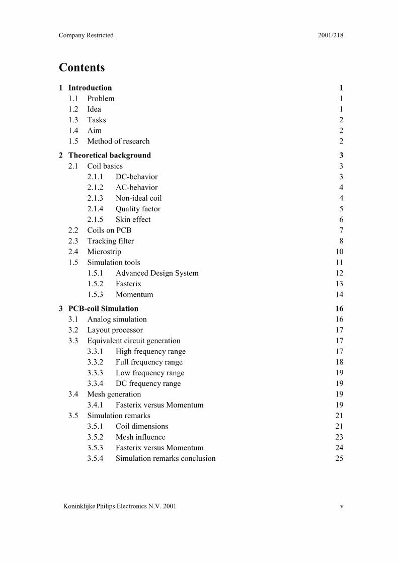
1 IntroductionIn the Integrated Transceivers department (reference [I1]) of Philips Research a new TV-tuner concept hasbeen defined. A TV-tuner adjusts the received signal (coming from air or antenna) for further demodula-tion. Today’s TV-tuners contain about thirty air-coils, which are mostly used for an analog filter-circuit.These air-coils are mostly manually aligned, which leads to an expensive TV-tuner. Within the projectgroup a new concept of receiving the TV-signal has been developed, which makes it possible to reduce thesize of a TV-tuner or even integrate it and make it adjustment-free.Figure 1-1 shows one of the first TV-tuners (at the back), followed by the current versions (front left andright) and the possible future version of the TV-tuner in chip-form (front middle).
1.1 ProblemOne of the problems of the new TV-tuner concept is that the integrated TV-tuner still contains air-coils.To replace the air-coils by planar coils, several parameters must be studied. For example, to see whether ahigh quality factor (20 or more), of the coil on PCB can be achieved. A coil has non-idealities like resistorand parasitic capacitance that disturb the coil behavior in a certain frequency range. To make sure that thecoils behave inductive, the limitations must be investigated and reported.
1.2 IdeaStudy whether it is possible that the simulation tools can simulate the inductance value and quality factorof a coil on PCB.Design and simulate the behavior of coils on PCB with the simulation tool Fastrix (figure1-2). Fasterix is developed by ED&T (reference [I2]) , for IC-design as well as PCB design for analog andmixed applications. Fasterix will help to comprehend the coil behavior and find out the advantages anddisadvantages of coils on the PCB. Both the quality factor and the inductance value will be simulated. Theaccuracy of the simulation can be evaluated by the measurements.
Figure 1-1 Past, present days and possible future TV-tuners.
Figure 1-2 Air-coil and PCB coil.
2001/218 Company Restricted
2 Koninklijke Philips Electronics N.V. 2001
1.3 TasksResearchStudy of the existing documentation about coils on PCB as well as study of the basic coil theory theirbehavior. Study of different simulation tools (Fasterix, Momentum, ADS-Schematics and Pstar).The measurement environment and the possibility of making a PCB-layout have to be inquired.
SimulationCalculation and simulation of the PCB coils behavior can be done with the EM simulation programFasterix. Fasterix calculates the electromagnetic field of a designed coil by solving the Maxwell equations.This makes it possible to simulate the inductance value and the quality factor of a coil. Simulation results,simulation methods and the considerations that have been made must be critically evaluated.
MeasurementThe accuracy of the simulation results will be confirmed by measurements of the designed PCB coils.The measurement environment is used as a reference for the simulation, to make sure that the results arecompatible.
Evaluation & ReportThe procedure and recommendations will be clearly documented. The simulation tools have to be evalu-ated. Simulation and measurement results must be compared and the possible difference reported. Positiveresults about the quality factor and behavior of the coil will lead to an integration of the designed coils intoa TV-tuner circuit. One of the important tasks is writing the report. The report will contain a short repre-sentation of the steps that have been done during the accomplishing of the assignment.
1.4 AimStudy the influences of different coils-shapes (on PCB) on the inductance value and quality factor bysimulations with Fasterix and ADS-Schematics. Study the possibility of achieving the wanted inductancevalue and quality factor using simulation tools as well as confirming the simulation results by measure-ment. Implementation of designed coils into the TV-tuner circuit.
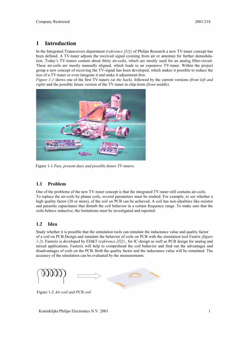
1.5 Method of researchThe method of research is similar to a BOTTOM-UP method as shown in figure 1-3. Studying the coilbehavior starts from the basics. This includes getting familiar with the simulation tools, deriving possibleequations for the inductance value and build other theoretical knowledge.The simulation and measurement results will be compared and reported. The evaluation of the interfacebetween simulation tools, Fasterix and ADS, is also necessary.
At the end of the assignment, the necessary conclusions and recommendations will be reported. Possibilityof integration of designed coils into the TV-tuner circuits will also be investigated and possible implemen-tation of the coils into a TV-circuit will be done.
Figure 1-3 BOTTOM-UP research method.
Research Simulation
Evaluation
Measurement Circuit Implementation
Company Restricted 2001/218
Koninklijke Philips Electronics N.V. 2001
UI bΖ
2 Theoretical backgroundCoils are used in a number of different applications and like capacitors (Appendix A.3) and resistors arepassive components. Different kind of coils exists for different applications. In energy techniques coils areused as transformers and current limited elements. RF coils are used in filters, resonance and tunablecircuits. Air-coils in a TV-tuner circuit are mainly used in filter or tuner circuits. The several coil parame-ters have a great influence on the quality factor and inductance value. To understand the behavior of a PCBcoil, first the general basics of coils are studied. The behavior of the tracking filter with coils on PCB mustbe the same as with air-coils in order to replace the air-coils with coils on PCB. Therefore the behavior ofthe tracking filter is studied. The properties of a microstrip are also studied, because they are needed whenmeasuring the coils. Different simulation tools such as ADS, Momentum and Fasterix are used to simulatethe coils on PCB.
2.1 Coil basicsTo understand the behavior of coils in general, documentation has been studied (reference [B7]). In thissection the basic coil theory will be represented, as following:- DC-behavior - Quality Factor- AC-behavior - Skin effect- Non-ideal coil
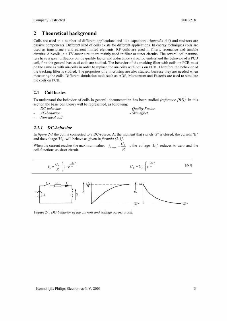
2.1.1 DC-behaviorIn figure 2-1 the coil is connected to a DC-source. At the moment that switch ‘S’ is closed, the current ‘IL‘and the voltage ‘UL’ will behave as given in for ula [2-1].
When the current reaches the maximum value, , the voltage ‘UL‘ reduces to zero and thecoil functions as short-circuit.
����
�ς�φ
Ο
LtR
bL e
RU
I 1
Figure 2-1 DC-behavior of the current and vol
m
3
RL max,
����
��φ
Ο
LtR
bL eUU [2-1]
tage across a coil.
2001/218 Company Restricted
4 Koninklijke Philips Electronics N.V. 2001
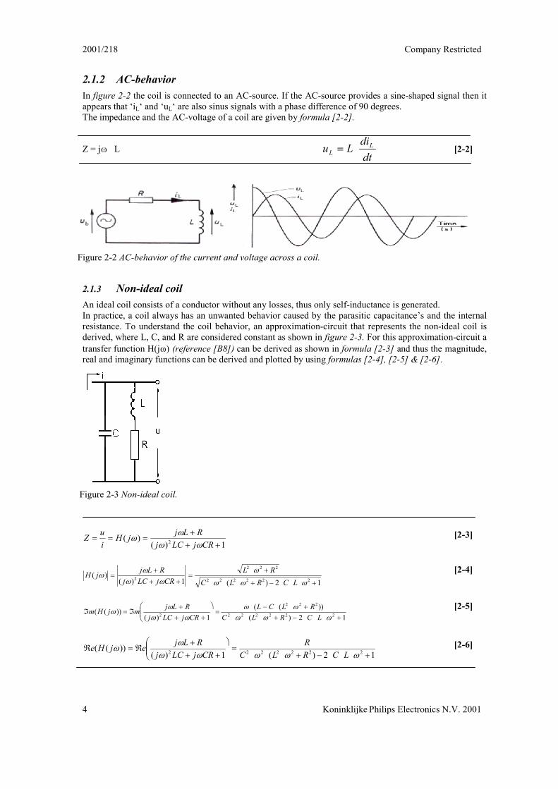
2.1.2 AC-behaviorIn figure 2-2 the coil is connected to an AC-source. If the AC-source provides a sine-shaped signal then itappears that ‘iL‘ and ‘uL‘ are also sinus signals with a phase difference of 90 degrees.The impedance and the AC-voltage of a coil are given by formula [2-2].
Z = j∂ L dtdiLu L
L _ [2-2]
2.1.3 Non-ideal coilAn ideal coil consists of a conductor without any losses, thus only self-inductance is generated.In practice, a coil always has an unwanted behavior caused by the parasitic capacitance’s and the internalresistance. To understand the coil behavior, an approximation-circuit that represents the non-ideal coil isderived, where L, C, and R are considered constant as shown in figure 2-3. For this approximation-circuit atransfer function H(j∂) (reference [B8]) can be derived as shown in formula [2-3] and thus the magnitude,real and imaginary functions can be derived and plotted by using formulas [2-4], [2-5] & [2-6].
1)()( 2
ΗΗ
ΗΖΖΖ
CRjLCjRLjjH
iuZ
∂∂
∂
∂[2-3]
12)(1)()(
222222
222
2ΗΟΗ
Η
_
ΗΗ
Η
_
∂∂∂
∂
∂∂
∂
∂
LCRLCRL
CRjLCjRLjjH [2-4]
12)())((
1)())(( 222222
222
2 ΗΟΗ
ΗΟ_
����
�
ΗΗ
Η�_�
∂∂∂
∂∂
∂∂
∂
∂
LCRLCRLCL
CRjLCjRLjmjHm [2-5]
12)(1)())(( 2222222 ΗΟΗ
_�
���
�
ΗΗ
Η�_�
∂∂∂∂∂
∂
∂
LCRLCR
CRjLCjRLjejHe [2-6]
Figure 2-2 AC-behavior of the current and voltage across a coil.
Figure 2-3 Non-ideal coil.
Company Restricted 2001/218
Koninklijke Philips Electronics N.V. 2001 5
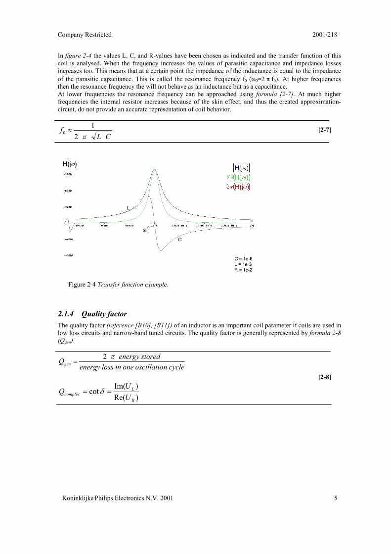
In figure 2-4 the values L, C, and R-values have been chosen as indicated and the transfer function of thiscoil is analysed. When the frequency increases the values of parasitic capacitance and impedance lossesincreases too. This means that at a certain point the impedance of the inductance is equal to the impedanceof the parasitic capacitance. This is called the resonance frequency f0 (∂0=2 × f0). At higher frequenciesthen the resonance frequency the will not behave as an inductance but as a capacitance.At lower frequencies the resonance frequency can be approached using formula [2-7]. At much higherfrequencies the internal resistor increases because of the skin effect, and thus the created approximation-circuit, do not provide an accurate representation of coil behavior.
CLf �
↓21
0 [2-7]
2.1.4 Quality factorThe quality factor (reference [B10], [B11]) of an inductor is an important coil parameter if coils are used inlow loss circuits and narrow-band tuned circuits. The quality factor is generally represented by formula 2-8(Qgen).
cyclenoscillatiooneinlossenergystoredenergyQgen _
↓2
[2-8]
)Re()Im(
cotR
Lcomplex U
UQ ΖΖ ≤
Figure 2-4 Transfer function example.
2001/218 Company Restricted
6 Koninklijke Philips Electronics N.V. 2001
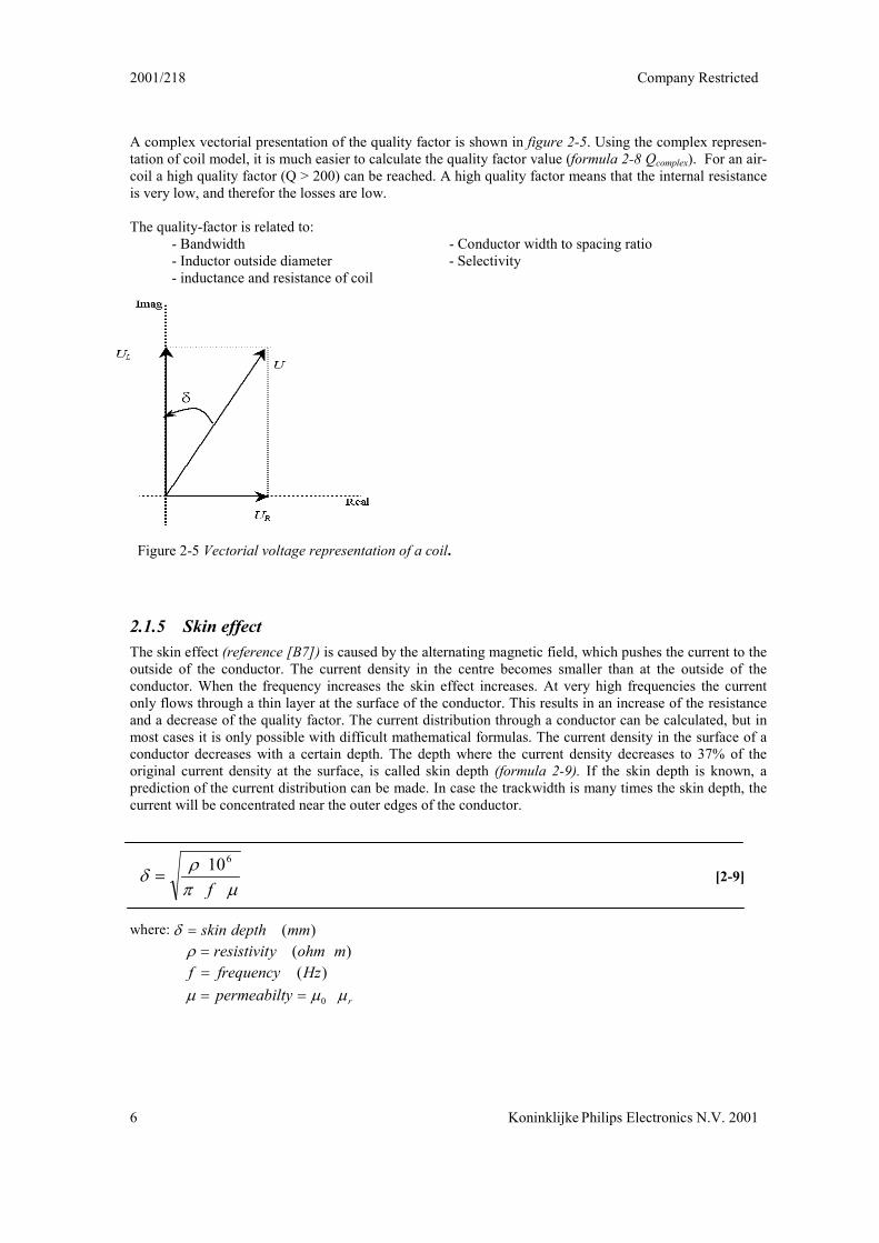
A complex vectorial presentation of the quality factor is shown in figure 2-5. Using the complex represen-tation of coil model, it is much easier to calculate the quality factor value (formula 2-8 Qcomplex). For an air-coil a high quality factor (Q > 200) can be reached. A high quality factor means that the internal resistanceis very low, and therefor the losses are low.
The quality-factor is related to:- Bandwidth - Conductor width to spacing ratio- Inductor outside diameter - Selectivity- inductance and resistance of coil
2.1.5 Skin effectThe skin effect (reference [B7]) is caused by the alternating magnetic field, which pushes the current to theoutside of the conductor. The current density in the centre becomes smaller than at the outside of theconductor. When the frequency increases the skin effect increases. At very high frequencies the currentonly flows through a thin layer at the surface of the conductor. This results in an increase of the resistanceand a decrease of the quality factor. The current distribution through a conductor can be calculated, but inmost cases it is only possible with difficult mathematical formulas. The current density in the surface of aconductor decreases with a certain depth. The depth where the current density decreases to 37% of theoriginal current density at the surface, is called skin depth (formula 2-9). If the skin depth is known, aprediction of the current distribution can be made. In case the trackwidth is many times the skin depth, thecurrent will be concentrated near the outer edges of the conductor.
←↓
±≤ _
f
610[2-9]
where: )(mmdepthskinΖ≤
)( mohmyresistivit_±
)(Hzfrequencyf Ζ
rypermeabilt ←←← __ 0
Figure 2-5 Vectorial voltage representation of a coil.
Company Restricted 2001/218
Koninklijke Philips Electronics N.V. 2001 7
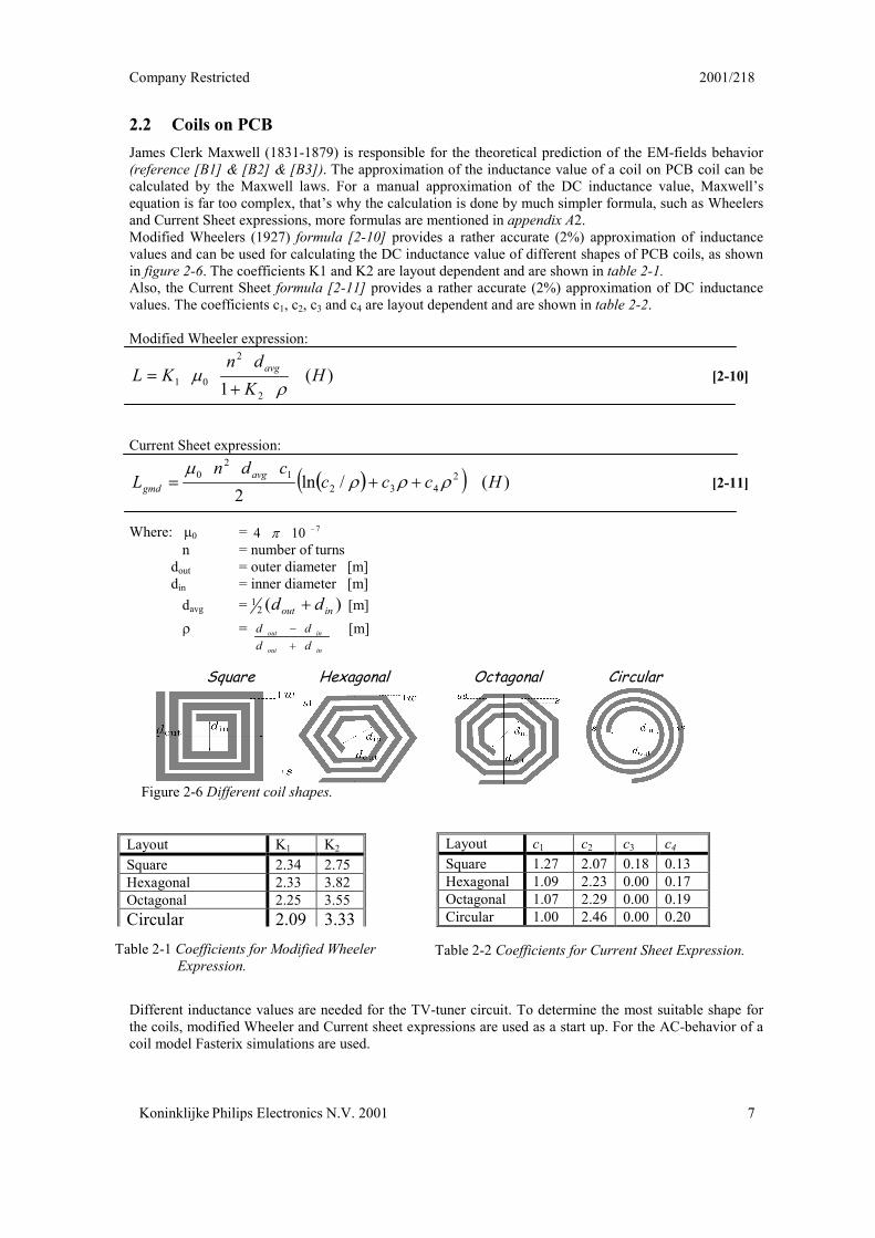
2.2 Coils on PCBJames Clerk Maxwell (1831-1879) is responsible for the theoretical prediction of the EM-fields behavior(reference [B1] & [B2] & [B3]). The approximation of the inductance value of a coil on PCB coil can becalculated by the Maxwell laws. For a manual approximation of the DC inductance value, Maxwell’sequation is far too complex, that’s why the calculation is done by much simpler formula, such as Wheelersand Current Sheet expressions, more formulas are mentioned in appendix A2.Modified Wheelers (1927) formula [2-10] provides a rather accurate (2%) approximation of inductancevalues and can be used for calculating the DC inductance value of different shapes of PCB coils, as shownin figure 2-6. The coefficients K1 and K2 are layout dependent and are shown in table 2-1.Also, the Current Sheet formula [2-11] provides a rather accurate (2%) approximation of DC inductancevalues. The coefficients c1, c2, c3 and c4 are layout dependent and are shown in table 2-2.
Modified Wheeler expression:
)(1 2
2
01 HK
dnKL avg
±←
Μ
_ [2-10]
Current Sheet expression:
Ε ΦΕ Φ )(/ln2
2432
12
0 Hccccdn
L avggmd ±±±
←ΗΗ_ [2-11]
Where: ←0 = 7104 ϑ
↓
n = number of turnsdout = outer diameter [m]din = inner diameter [m]
davg = )(21
inout dd Η [m]± =
inout
inout
dddd
Η
ϑ [m]
Different inductance values are needed for the TV-tuner circuit. To determine the most suitable shape forthe coils, modified Wheeler and Current sheet expressions are used as a start up. For the AC-behavior of acoil model Fasterix simulations are used.
Square Hexagonal Octagonal Circular
Figure 2-6 Different coil shapes.
Table 2-1 Coefficients for Modified WheelerExpression.
Table 2-2 Coefficients for Current Sheet Expression.
Layout K1 K2
Square 2.34 2.75Hexagonal 2.33 3.82Octagonal 2.25 3.55Circular 2.09 3.33
Layout c1 c2 c3 c4
Square 1.27 2.07 0.18 0.13Hexagonal 1.09 2.23 0.00 0.17Octagonal 1.07 2.29 0.00 0.19Circular 1.00 2.46 0.00 0.20
2001/218 Company Restricted
8 Koninklijke Philips Electronics N.V. 2001
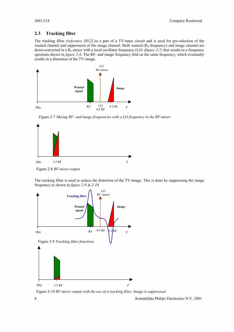
2.3 Tracking filterThe tracking filter (reference [B12],)is a part of a TV-tuner circuit and is used for pre-selection of thewanted channel and suppression of the image channel. Both wanted (RF-frequency) and image channel aredown-converted in a RF-mixer with a local oscillator frequency (LO) (figure 2-7) that results in a frequencyspectrum shown in figure 2-8. The RF- and image frequency fold on the same frequency, which eventuallyresults in a distortion of the TV-image.
The tracking filter is used to reduce the distortion of the TV-image. This is done by suppressing the imagefrequency as shown in figure 2-9 & 2-10.
Figure 2-7 Mixing RF- and image frequencies with a LO frequency in the RF-mixer.
Figure 2-8 RF-mixer output.
Figure 2-9 Tracking filter functions.
Figure 2-10 RF-mixer output with the use of a tracking filter. Image is suppressed.f0Hz 1/3 RF
ImageWantedsignal
f0Hz RF 5/3 RF
LORF mixer
4/3 RF
Tracking filter
f0Hz 1/3 RF
f0Hz RF 5/3 RF
LO RF-mixer
LO4/3 RF
ImageWantedsignal
Company Restricted 2001/218
Koninklijke Philips Electronics N.V. 2001 9
Vtune
Varicap
Couplinginductor
B
A
SignalIn
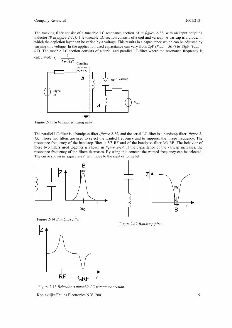
The tracking filter consist of a tuneable LC resonance section (A in figure 2-11) with an input couplinginductor (B in figure 2-11). The tuneable LC section consists of a coil and varicap. A varicap is a diode, inwhich the depletion layer can be varied by a voltage. This results in a capacitance which can be adjusted byvarying this voltage. In the application used capacitance can vary from 2pF (Vtune = 30V) to 18pF (Vtune =0V). The tunable LC section consists of a serial and parallel LC-filter where the resonance frequency iscalculated:
LCf
↓21
0 Ζ.
The parallel LC-filter is a bandpass filter (figure 2-12) and the serial LC-filter is a bandstop filter (figure 2-13). These two filters are used to select the wanted frequency and to suppress the image frequency. Theresonance frequency of the bandstop filter is 5/3 RF and of the bandpass filter 3/3 RF. The behavior ofthese two filters used together is shown in figure 2-14. If the capacitance of the varicap increases, theresonance frequency of the filters decreases. By using this concept the wanted frequency can be selected.The curve shown in figure 2-14 will move to the right or to the left.
Figure 2-11 Schematic tracking filter.
Figure 2-12 Bandstop filter.
Figure 2-13 Behavior a tuneable LC resonance section.
Figure 2-14 Bandpass filter.
f
Z
∂0
B
f
Z
∂0
B
f
Z
RF 5/3RF
2001/218 Company Restricted
10 Koninklijke Philips Electronics N.V. 2001
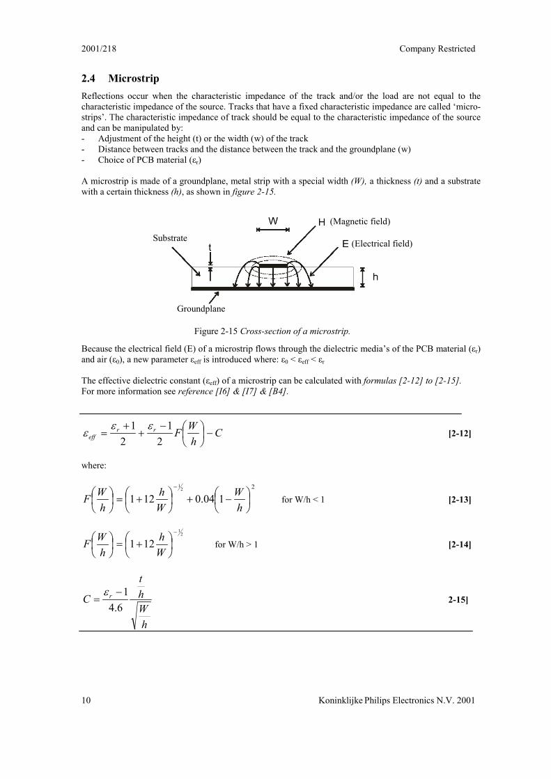
2.4 MicrostripReflections occur when the characteristic impedance of the track and/or the load are not equal to thecharacteristic impedance of the source. Tracks that have a fixed characteristic impedance are called ‘micro-strips’. The characteristic impedance of track should be equal to the characteristic impedance of the sourceand can be manipulated by:- Adjustment of the height (t) or the width (w) of the track- Distance between tracks and the distance between the track and the groundplane (w)- Choice of PCB material (εr)
A microstrip is made of a groundplane, metal strip with a special width (W), a thickness (t) and a substratewith a certain thickness (h), as shown in figure 2-15.
Because the electrical field (E) of a microstrip flows through the dielectric media’s of the PCB material (εr)and air (ε0), a new parameter εeff is introduced where: ε0 < εeff < εr
The effective dielectric constant (εeff) of a microstrip can be calculated with formulas [2-12] to [2-15].For more information see reference [I6] & [I7] & [B4].
Ch
WFrreff }�
�
���
�}{
{↓
21
21 ⋅⋅
⋅ [2-12]
where:
2
104.01212
1
��
���
�}{�
�
���
�{↓�
�
���
�}
hW
Wh
hWF for W/h < 1 [2-13]
21
121}
��
���
�{↓�
�
���
�
Wh
hWF for W/h > 1 [2-14]
hWht
C r
6.41}
↓
⋅
2-15]
Figure 2-15 Cross-section of a microstrip.
Substrate
Groundplane
(Magnetic field)
(Electrical field)
Company Restricted 2001/218
� Koninklijke Philips Electronics N.V. 2001 11
The microstrip that is needed for the measurement must have a characteristic impedance of 50ohm, be-cause the LCR-meter has an impedance of 50ohm. When these two are not equal reflections are introduced,which have a negative influence on the measurements. The characteristic impedance (Z0) of a microstip,with known dimensions and PCB material, can be calculated by formula [2-16], (reference [I6] & [I7])
���
�
���
�
�
{��{{�
�
{�
↓
)44.1(ln667.0393.11120
48ln60
0
hWhW
hW
Wh
Z
eff
eff
⋅
⋅
[2-16]
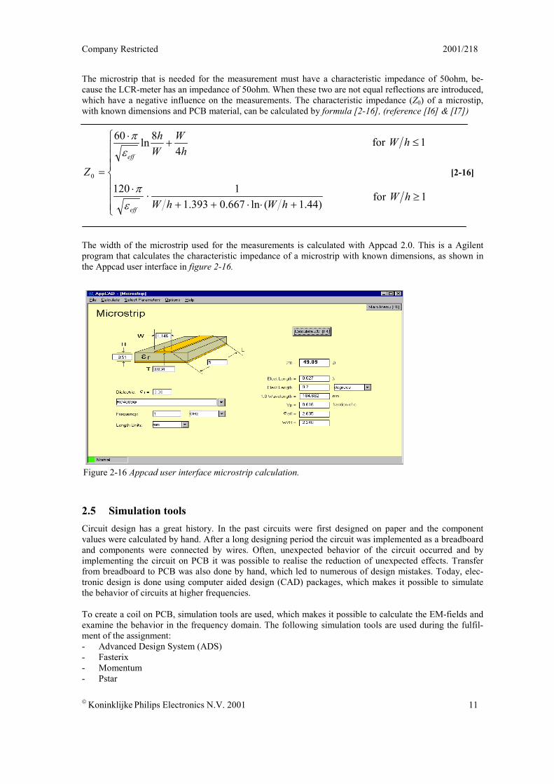
The width of the microstrip used for the measurements is calculated with Appcad 2.0. This is a Agilentprogram that calculates the characteristic impedance of a microstrip with known dimensions, as shown inthe Appcad user interface in figure 2-16.
2.5 Simulation toolsCircuit design has a great history. In the past circuits were first designed on paper and the componentvalues were calculated by hand. After a long designing period the circuit was implemented as a breadboardand components were connected by wires. Often, unexpected behavior of the circuit occurred and byimplementing the circuit on PCB it was possible to realise the reduction of unexpected effects. Transferfrom breadboard to PCB was also done by hand, which led to numerous of design mistakes. Today, elec-tronic design is done using computer aided design (CAD) packages, which makes it possible to simulatethe behavior of circuits at higher frequencies.
To create a coil on PCB, simulation tools are used, which makes it possible to calculate the EM-fields andexamine the behavior in the frequency domain. The following simulation tools are used during the fulfil-ment of the assignment:- Advanced Design System (ADS)- Fasterix- Momentum- Pstar
Figure 2-16 Appcad user interface microstrip calculation.
for 1�hW
for 1�hW
2001/218 Company Restricted
12 �Koninklijke Philips Electronics N.V. 2001
To simulate PCB design behavior, the following substrate and metallization parameters has to be specified:
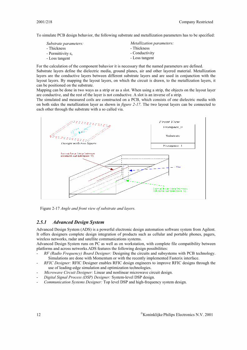
For the calculation of the component bahavior it is necessary that the named parameters are defined.Substrate layers define the dielectric media, ground planes, air and other layered material. Metallizationlayers are the conductive layers between different substrate layers and are used in conjunction with thelayout layers. By mapping the layout layers, on which the circuit is drawn, to the metallization layers, itcan be positioned on the substrate.Mapping can be done in two ways as a strip or as a slot. When using a strip, the objects on the layout layerare conductive, and the rest of the layer is not conductive. A slot is an inverse of a strip.The simulated and measured coils are constructed on a PCB, which consists of one dielectric media withon both sides the metallization layer as shown in figure 2-17. The two layout layers can be connected toeach other through the substrate with a so called via.
2.5.1 Advanced Design SystemAdvanced Design System (ADS) is a powerful electronic design automation software system from Agilent.It offers designers complete design integration of products such as cellular and portable phones, pagers,wireless networks, radar and satellite communications systems.Advanced Design System runs on PC as well as on workstation, with complete file compatibility betweenplatforms and across networks.ADS features the following design possibilities:- RF (Radio Frequency) Board Designer: Designing the circuits and subsystems with PCB technology.
Simulations are done with Momentum or with the recently implemented Fasterix interface.- RFIC Designer: RFIC Designer enables RFIC design engineers to improve RFIC designs through the
use of leading-edge simulation and optimization technologies.- Microwave Circuit Designer: Linear and nonlinear microwave circuit design.- Digital Signal Process (DSP) Designer: System-level DSP design.- Communication Systems Designer: Top level DSP and high-frequency system design.
Figure 2-17 Angle and front view of substrate and layers.
Substrate parameters: - Thickness- Permittivity ⁄r- Loss tangent
Metallization parameters: - Thickness- Conductivity- Loss tangent
Company Restricted 2001/218
� Koninklijke Philips Electronics N.V. 2001 13
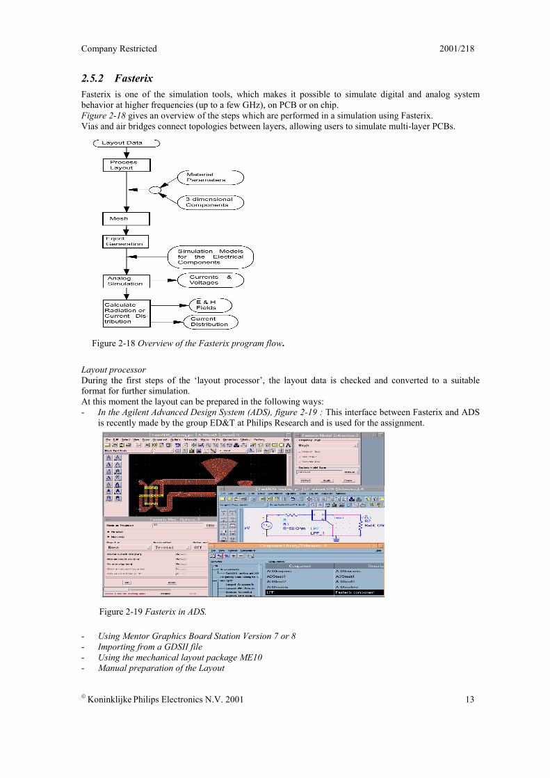
2.5.2 FasterixFasterix is one of the simulation tools, which makes it possible to simulate digital and analog systembehavior at higher frequencies (up to a few GHz), on PCB or on chip.Figure 2-18 gives an overview of the steps which are performed in a simulation using Fasterix.Vias and air bridges connect topologies between layers, allowing users to simulate multi-layer PCBs.
Layout processorDuring the first steps of the ‘layout processor’, the layout data is checked and converted to a suitableformat for further simulation.At this moment the layout can be prepared in the following ways:- In the Agilent Advanced Design System (ADS), figure 2-19 : This interface between Fasterix and ADS
is recently made by the group ED&T at Philips Research and is used for the assignment.
- Using Mentor Graphics Board Station Version 7 or 8- Importing from a GDSII file- Using the mechanical layout package ME10- Manual preparation of the Layout
Figure 2-18 Overview of the Fasterix program flow.
Figure 2-19 Fasterix in ADS.
2001/218 Company Restricted
14 �Koninklijke Philips Electronics N.V. 2001
If the layout process is completed successfully, the data of the following parameters are provided:- Material (dielectric constants, conductivity)- Dimensional component (screen, wires and cables)
Mesh GeneratorThe mesh generator divides the layout into a number of elements (as shown in chapter 3.4). The number ofelements determines the accuracy of the calculated parasitic (R, L, C) parameters of the layout. The num-ber of elements is determined by defined maximum frequency for which the generated equivalent circuitmodel of the layout must be valid.
Equivalent circuit generatorThe equivalent circuit generator’ calculates the values of the parasitic components R, L, C between parts ofthe layout. The results of this operation are an equivalent circuit model as shown in figure 2-20. In theADS-Schematic window it is now possible to connect the defined pins to a source.
Analog simulationThe analog simulation can be done in the ADS schematic environment as well as in Pstar. Using theequivalent circuit model made by Fasterix, the usual procedure of simulating a circuit can be done in theADS-Schematic window. For more information about Fasterix see the references site I3, I4 and I5.
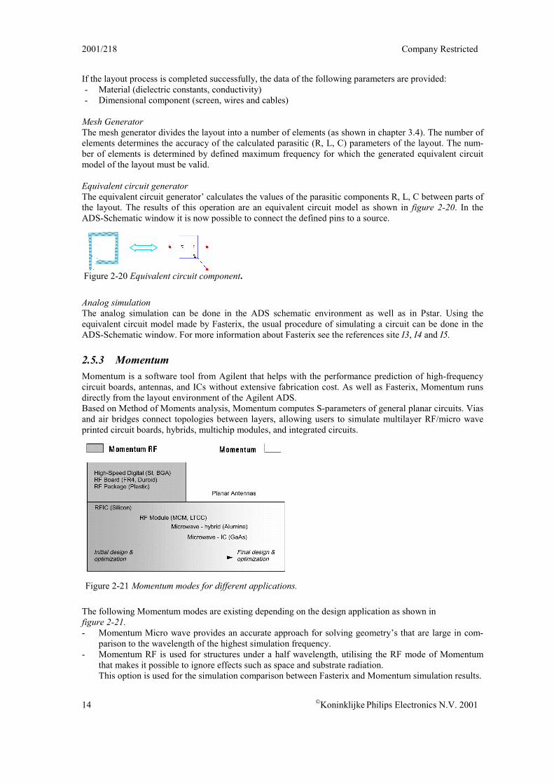
2.5.3 MomentumMomentum is a software tool from Agilent that helps with the performance prediction of high-frequencycircuit boards, antennas, and ICs without extensive fabrication cost. As well as Fasterix, Momentum runsdirectly from the layout environment of the Agilent ADS.Based on Method of Moments analysis, Momentum computes S-parameters of general planar circuits. Viasand air bridges connect topologies between layers, allowing users to simulate multilayer RF/micro waveprinted circuit boards, hybrids, multichip modules, and integrated circuits.
The following Momentum modes are existing depending on the design application as shown infigure 2-21.- Momentum Micro wave provides an accurate approach for solving geometry’s that are large in com-
parison to the wavelength of the highest simulation frequency.- Momentum RF is used for structures under a half wavelength, utilising the RF mode of Momentum
that makes it possible to ignore effects such as space and substrate radiation.This option is used for the simulation comparison between Fasterix and Momentum simulation results.
Figure 2-20 Equivalent circuit component.
Figure 2-21 Momentum modes for different applications.
Company Restricted 2001/218
� Koninklijke Philips Electronics N.V. 2001 15
Layout processorThe layout data is prepared in the Agilent ADS or is imported from another design tool. ADS can importfiles in a variety of formats.
Mesh GeneratorSame function as Fasterix mesh, only the different algorithm for generation of mesh is used and thus thedifference in the simulation time is introduced.
Output formatOutput chart formats include Cartesian and Smith charts, tabular listings that differ from the Fasterix‘equivalent circuit’ output file.
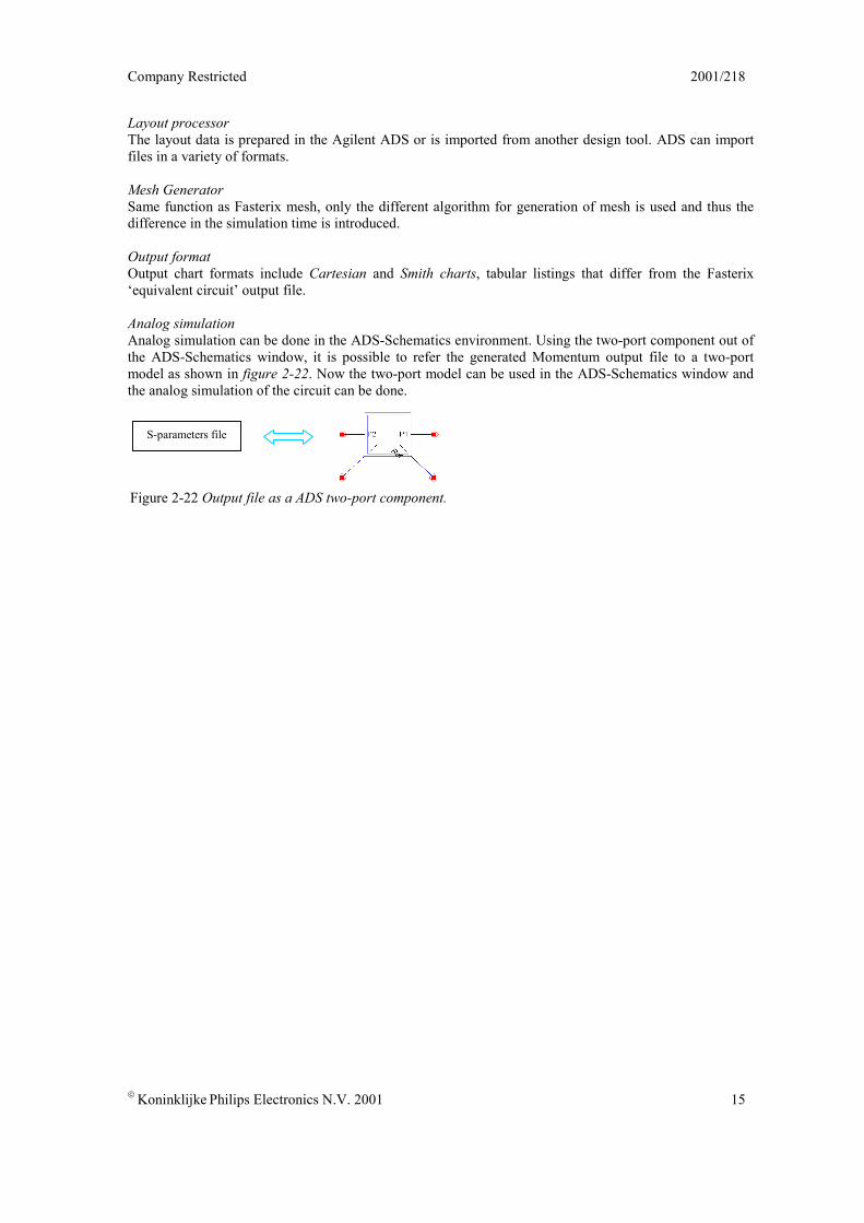
Analog simulationAnalog simulation can be done in the ADS-Schematics environment. Using the two-port component out ofthe ADS-Schematics window, it is possible to refer the generated Momentum output file to a two-portmodel as shown in figure 2-22. Now the two-port model can be used in the ADS-Schematics window andthe analog simulation of the circuit can be done.
Figure 2-22 Output file as a ADS two-port component.
S-parameters file
2001/218 Company Restricted
16 �Koninklijke Philips Electronics N.V. 2001
UL
(Imag )
Ur (Real)
U (Mag)
3 PCB-coil Simulation
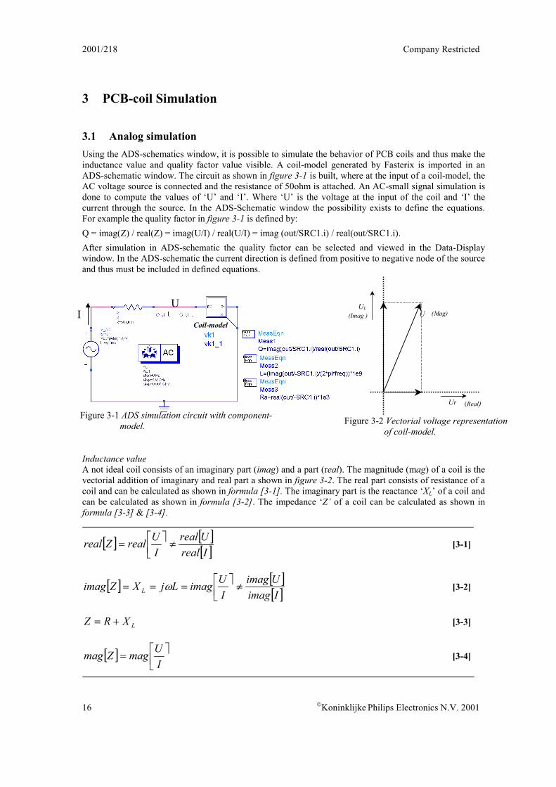
3.1 Analog simulationUsing the ADS-schematics window, it is possible to simulate the behavior of PCB coils and thus make theinductance value and quality factor value visible. A coil-model generated by Fasterix is imported in anADS-schematic window. The circuit as shown in figure 3-1 is built, where at the input of a coil-model, theAC voltage source is connected and the resistance of 50ohm is attached. An AC-small signal simulation isdone to compute the values of ‘U’ and ‘I’. Where ‘U’ is the voltage at the input of the coil and ‘I’ thecurrent through the source. In the ADS-Schematic window the possibility exists to define the equations.For example the quality factor in figure 3-1 is defined by:Q = imag(Z) / real(Z) = imag(U/I) / real(U/I) = imag (out/SRC1.i) / real(out/SRC1.i).After simulation in ADS-schematic the quality factor can be selected and viewed in the Data-Displaywindow. In the ADS-schematic the current direction is defined from positive to negative node of the sourceand thus must be included in defined equations.
Inductance valueA not ideal coil consists of an imaginary part (imag) and a part (real). The magnitude (mag) of a coil is thevectorial addition of imaginary and real part a shown in figure 3-2. The real part consists of resistance of acoil and can be calculated as shown in formula [3-1]. The imaginary part is the reactance ‘XL’ of a coil andcan be calculated as shown in formula [3-2]. The impedance ‘Z’ of a coil can be calculated as shown informula [3-3] & [3-4].
ξ ζξ ζξ ζIrealUreal
IUrealZreal �
��
�γ [3-1]
ξ ζξ ζξ ζIimagUimag
IUimagLjXZimag L �
��
�γγγ ∂ [3-2]
LXRZ ΗΖ [3-3]
ξ ζ ���
�γ
IUmagZmag [3-4]
Figure 3-1 ADS simulation circuit with component-model. Figure 3-2 Vectorial voltage representation
of coil-model.
Coil-modelI
U
Company Restricted 2001/218
� Koninklijke Philips Electronics N.V. 2001 17
The imaginary part of a coil-model represents the inductance value and is defined as shown informula [3-5].
Ε ΦfI
UimagL ���
�γ ↓2 [3-5]
The quality factorThe quality factor of the Fasterix coil-model can be calculated by dividing the imaginary and real part ofthe coil-model, according to formula 3-6.
ξ ζ ξ ζ ���
���
��
�γγγ
IUreal
IUimagZrealZimagR
XQ L [3-6]
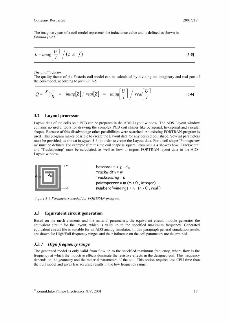
3.2 Layout processorLayout data of the coils on a PCB can be prepared in the ADS-Layout window. The ADS-Layout windowcontains no useful tools for drawing the complex PCB coil shapes like octagonal, hexagonal and circularshapes. Because of this disadvantage other possibilities were searched. An existing FORTRAN-program isused. This program makes possible to create the Layout data for any desired coil shape. Several parametersmust be provided, as shown in figure 3-3, in order to create the Layout data. For a coil shape ‘Pointsperrevm’ must be defined. For example if m = 4 the coil shape is square. Appendix A.4 showns how ‘Trackwidth’and ‘Trackspacing’ must be calculated, as well as how to import FORTRAN layout data in the ADS-Layout window.
3.3 Equivalent circuit generationBased on the mesh elements and the material parameters, the equivalent circuit module generates theequivalent circuit for the layout, which is valid up to the specified maximum frequency. Generatedequivalent circuit file is suitable for an ADS analog simulator. In this paragraph general simulation resultsare shown for High/Full frequency ranges and their influence on the coil parameters are determined.
3.3.1 High frequency rangeThe generated model is only valid from flow up to the specified maximum frequency, where flow is thefrequency at which the inductive effects dominate the resistive effects in the designed coil. This frequencydepends on the geometry and the material parameters of the coil. This option requires less CPU time thanthe Full model and gives less accurate results in the low frequency range.
Figure 3-3 Parameters needed for FORTRAN-program.
baseradius = ½ � din
trackwidth = w trackspacing = s pointsperrev = m (m > 0 , integer) numberofwindings = n (n > 0 , real )
2001/218 Company Restricted
18 �Koninklijke Philips Electronics N.V. 2001
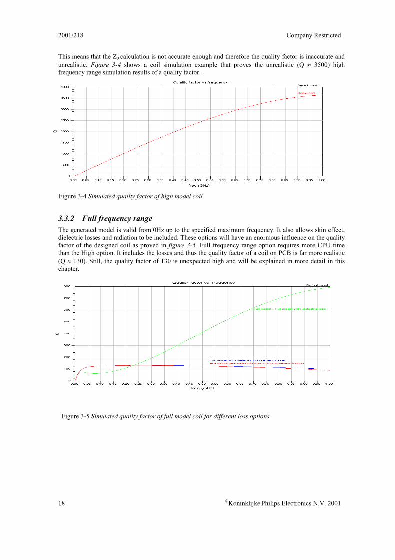
This means that the Z0 calculation is not accurate enough and therefore the quality factor is inaccurate andunrealistic. Figure 3-4 shows a coil simulation example that proves the unrealistic (Q � 3500) highfrequency range simulation results of a quality factor.
3.3.2 Full frequency rangeThe generated model is valid from 0Hz up to the specified maximum frequency. It also allows skin effect,dielectric losses and radiation to be included. These options will have an enormous influence on the qualityfactor of the designed coil as proved in figure 3-5. Full frequency range option requires more CPU timethan the High option. It includes the losses and thus the quality factor of a coil on PCB is far more realistic(Q � 130). Still, the quality factor of 130 is unexpected high and will be explained in more detail in thischapter.
Figure 3-4 Simulated quality factor of high model coil.
Figure 3-5 Simulated quality factor of full model coil for different loss options.
Company Restricted 2001/218
� Koninklijke Philips Electronics N.V. 2001 19
3.3.3 Low frequency rangeThis model is only valid for low frequencies, which cannot be used for an accurate simulation in frequencydomain. This option is not suitable for the use of assignment because of the inaccurate results.
3.3.4 DC frequency rangeThe generated model is only valid for zero frequencies and only contains the parasitic resistor. This optionis not suitable for the use of assignment because of the inaccurate results.
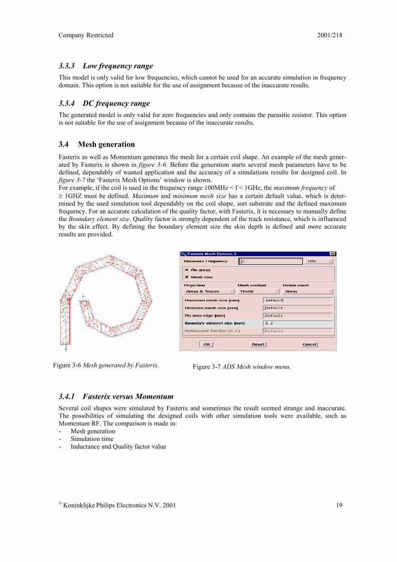
3.4 Mesh generationFasterix as well as Momentum generates the mesh for a certain coil shape. An example of the mesh gener-ated by Fasterix is shown in figure 3-6. Before the generation starts several mesh parameters have to bedefined, dependably of wanted application and the accuracy of a simulations results for designed coil. Infigure 3-7 the ‘Fasterix Mesh Options’ window is shown.For example, if the coil is used in the frequency range 100MHz < f < 1GHz, the maximum frequency of� 1GHZ must be defined. Maximum and minimum mesh size has a certain default value, which is deter-mined by the used simulation tool dependably on the coil shape, sort substrate and the defined maximumfrequency. For an accurate calculation of the quality factor, with Fasterix, it is necessary to manually definethe Boundary element size. Quality factor is strongly dependent of the track resistance, which is influencedby the skin effect. By defining the boundary element size the skin depth is defined and more accurateresults are provided.
3.4.1 Fasterix versus MomentumSeveral coil shapes were simulated by Fasterix and sometimes the result seemed strange and inaccurate.The possibilities of simulating the designed coils with other simulation tools were available, such asMomentum RF. The comparison is made in:- Mesh generation- Simulation time- Inductance and Quality factor value
Figure 3-6 Mesh generated by Fasterix. Figure 3-7 ADS Mesh window menu.
2001/218 Company Restricted
20 �Koninklijke Philips Electronics N.V. 2001
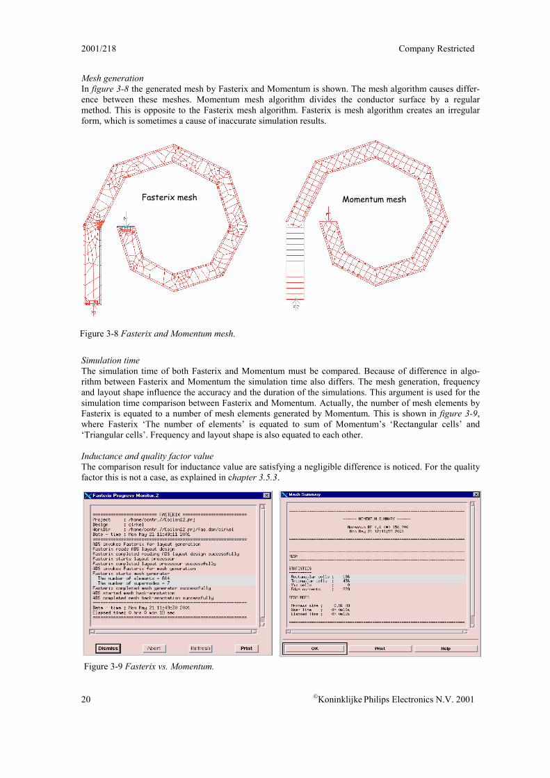
Fasterix mesh Momentum mesh
Mesh generationIn figure 3-8 the generated mesh by Fasterix and Momentum is shown. The mesh algorithm causes differ-ence between these meshes. Momentum mesh algorithm divides the conductor surface by a regularmethod. This is opposite to the Fasterix mesh algorithm. Fasterix is mesh algorithm creates an irregularform, which is sometimes a cause of inaccurate simulation results.
Simulation timeThe simulation time of both Fasterix and Momentum must be compared. Because of difference in algo-rithm between Fasterix and Momentum the simulation time also differs. The mesh generation, frequencyand layout shape influence the accuracy and the duration of the simulations. This argument is used for thesimulation time comparison between Fasterix and Momentum. Actually, the number of mesh elements byFasterix is equated to a number of mesh elements generated by Momentum. This is shown in figure 3-9,where Fasterix ‘The number of elements’ is equated to sum of Momentum’s ‘Rectangular cells’ and‘Triangular cells’. Frequency and layout shape is also equated to each other.
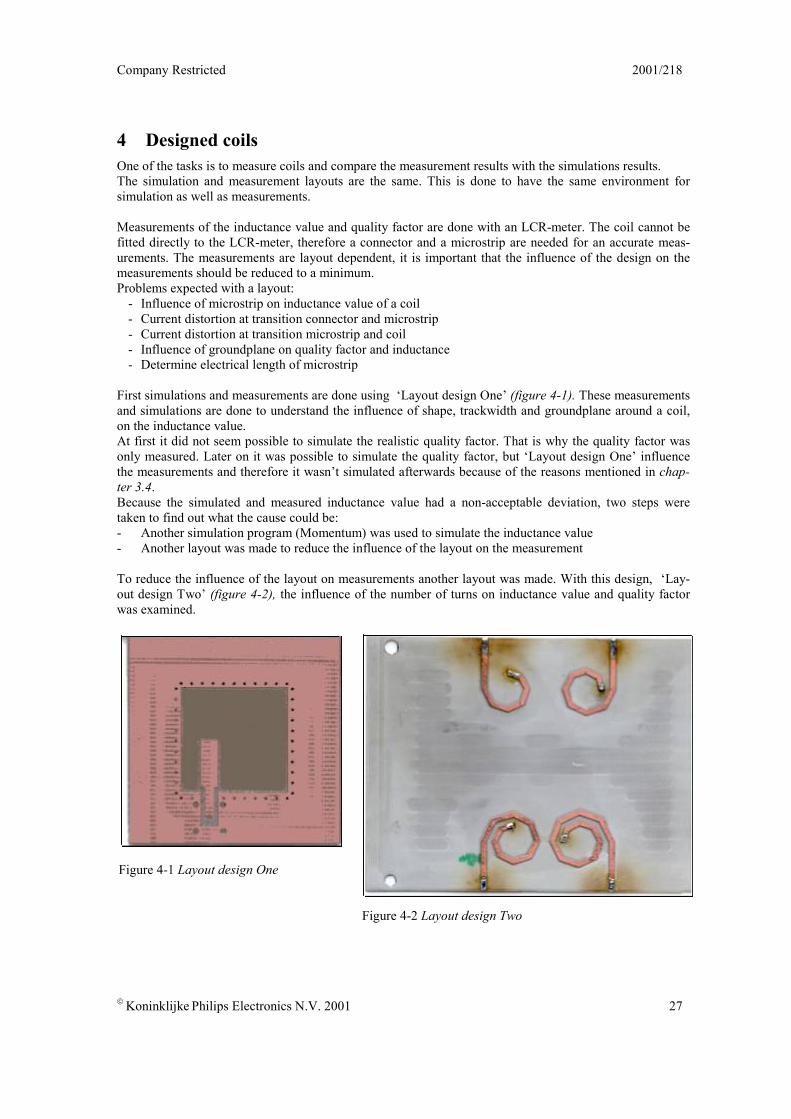
Inductance and quality factor valueThe comparison result for inductance value are satisfying a negligible difference is noticed. For the qualityfactor this is not a case, as explained in chapter 3.5.3.
Figure 3-8 Fasterix and Momentum mesh.
Figure 3-9 Fasterix vs. Momentum.
Company Restricted 2001/218
� Koninklijke Philips Electronics N.V. 2001 21
3.5 Simulation remarksThis paragraph provides several remarks on the simulation tools and coil dimensions. Remarks are mainlymade on the inductance and quality factor simulation values. Influences of changing the simulation pa-rameters and the coil dimensions on these values are examined. Especially the mesh ‘Boundary elementsize’ causes the difficulties for an accurate Fasterix simulation of quality factor.
The following parameters/simulation tools have been changed:- Coil dimensions
- Number of turns- Variation in baseradius, trackwidth and trackspacing- Dielectric media- Vias
- Mesh variation- Fasterix versus Momentum
3.5.1 Coil dimensionsIn this paragraph the influence of coil shape parameters on the inductance and quality factors are shownand explained by means of examples and graphics. Hexagonal, octagonal, square and circular coil shapesare used.
Number of turnsThe influence of the varying dimension parameters (of the coil on PCB) on the inductance and qualityfactor are simulated. Hexagonal, octagonal, square and circular coil shapes are used.The trackwidth and trackspacing are equal to 1mm. The base radius is equal to 2.5mm. The number of turn’n’ is changed from n = 1 to n = 2.
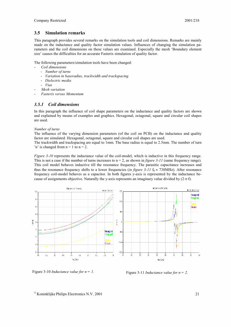
Figure 3-10 represents the inductance value of the coil-model, which is inductive in this frequency range.This is not a case if the number of turns increases to n = 2, as shown in figure 3-11 (same frequency range).This coil model behaves inductive till the resonance frequency. The parasitic capacitance increases andthus the resonance frequency shifts to a lower frequencies (in figure 3-11 f0 � 730MHz). After resonancefrequency coil-model behaves as a capacitor. In both figures y-axis is represented by the inductance be-cause of assignments objective. Naturally the y-axis represents an imaginary value divided by (2�∨�f).
Figure 3-10 Inductance value for n = 1. Figure 3-11 Inductance value for n = 2.
2001/218 Company Restricted
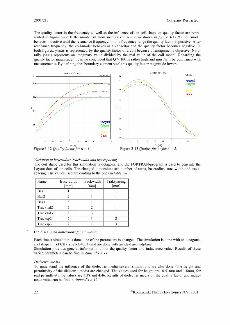
The quality factor in the frequency as well as the influence of the coil shape on quality factor are repre-sented in figure 3-12. If the number of turns increases to n = 2, as shown in figure 3-13 the coil modelbehaves inductive until the resonance frequency. In this frequency range the quality factor is positive. Afterresonance frequency, the coil-model behaves as a capacitor and the quality factor becomes negative. Inboth figures, y-axis is represented by the quality factor of a coil because of assignments objective. Natu-rally y-axis represents an imaginary value divided by the real value of the coil model. Regarding thequality factor magnitude, it can be concluded that Q > 100 is rather high and must/will be confirmed withmeasurements. By defining the ‘boundary element size’ this quality factor magnitude lowers.
Variation in baseradius, trackwidth and trackspacingThe coil shape used for this simulation is octagonal and the FORTRAN-program is used to generate theLayout data of the coils. The changed dimensions are number of turns, baseradius. trackwidth and track-
Figure 3-12 Quality factor for n = 1. Figure 3-13 Quality factor for n = 2.
Name Baseradius[mm]
Trackwidth[mm]
Trakspacing[mm]
Bas1 1 1 1Bas2 2 1 1Bas3 3 1 1Trackwd2 2 2 1Trackwd3 2 3 1Tracksp2 2 1 2Tracksp3 2 1 3
.
spacing. The values used are cording to the ones in table 3-1.
22 �Koninklijke Philips Electronics N.V. 2001
Each time a simulation is done, one of the parameters is changed. The simulation is done with an octagonalcoil shape on a PCB (type RO4003) and are done with an ideal groundplane.Simulation provides general information about the quality factor and inductance value. Results of thesevaried parameters can be find in Appendix A.11.
Dielectric mediaTo understand the influence of the dielectric media several simulations are also done. The height andpermittivity of the dielectric media are changed. The values used for height are 0.51mm and 1.8mm, forreal permittivity the values are 3.38 and 4.46. Results of dielectric media on the quality factor and induc-tance value can be find in Appendix A.12.
Table 3-1 Used dimensions for simulation.
Company Restricted 2001/218
� Koninklijke Philips Electronics N.V. 2001 23
baseradius = 2.5mm trackwidth = 1mm trackspacing = 1mm pointsperrev = 30, circular
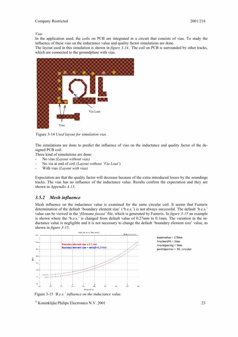
ViasIn the application used, the coils on PCB are integrated in a circuit that consists of vias. To study theinfluence of these vias on the inductance value and quality factor simulations are done.The layout used in this simulation is shown in figure 3.14. The coil on PCB is surrounded by other tracks,which are connected to the groundplane with vias.
The simulations are done to predict the influence of vias on the inductance and quality factor of the de-signed PCB coil.Three kind of simulations are done:- No vias (Layout without vias)- No via at end of coil (Layout without ‘Via Lout’)- With vias (Layout with vias)
Expectation are that the quality factor will decrease because of the extra introduced losses by the soundingstracks. The vias has no influence of the inductance value. Results confirm the expectation and they areshown in Appendix A.13.
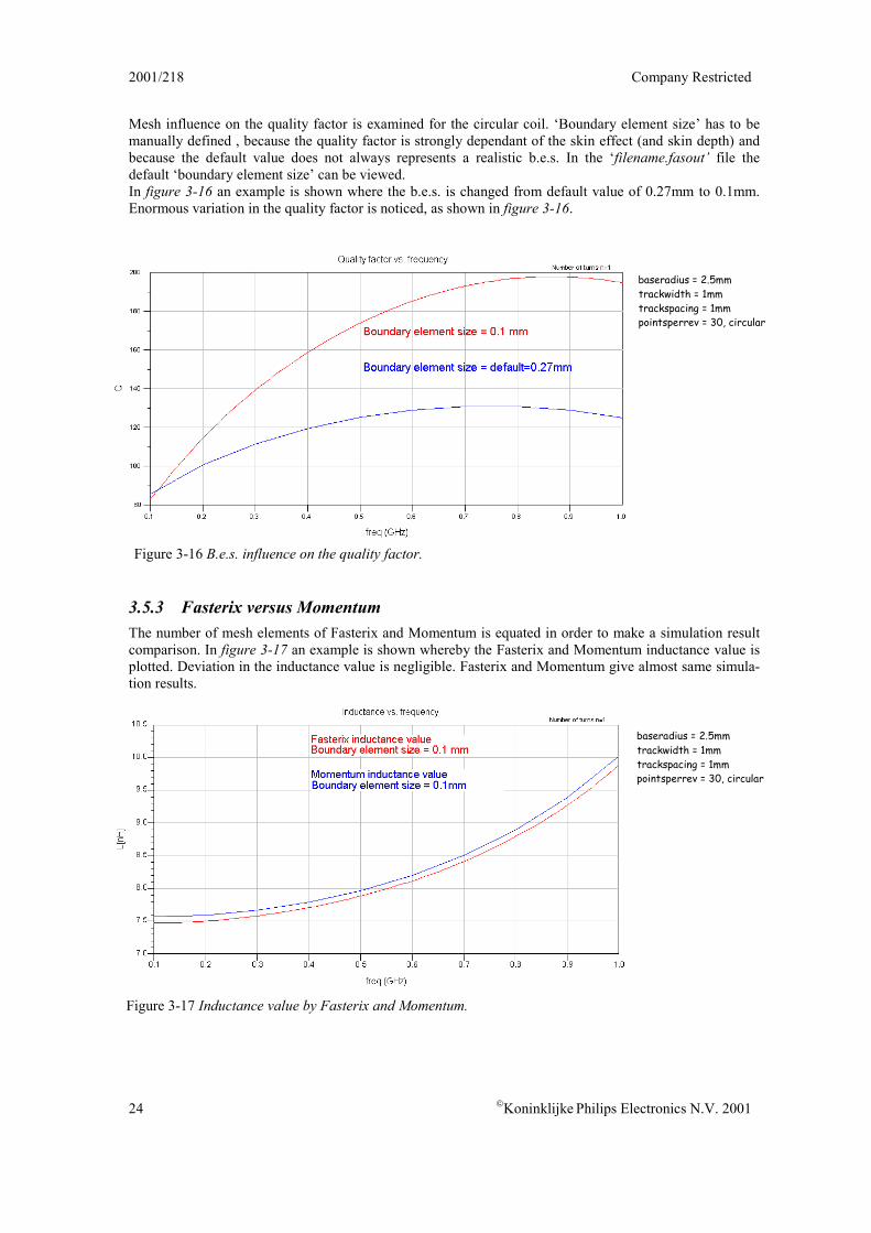
3.5.2 Mesh influenceMesh influence on the inductance value is examined for the same circular coil. It seems that Fasterixdetermination of the default ‘boundary element size’ (‘b.e.s.’) is not always successful. The default ‘b.e.s.’value can be viewed in the ‘filename.fasout’ file, which is generated by Fasterix. In figure 3-15 an exampleis shown where the ‘b.e.s.’ is changed from default value of 0.27mm to 0.1mm. The variation in the in-ductance value is negligible and it is not necessary to change the default ‘boundary element size’ value, asshown in figure 3-15.
Figure 3-14 Used layout for simulation vias.
Figure 3-15 ‘B.e.s.’ influence on the inductance value.
Via Lout
Vias
2001/218 Company Restricted
24 �Koninklijke Philips Electronics N.V. 2001
baseradius = 2.5mm trackwidth = 1mm trackspacing = 1mm pointsperrev = 30, circular
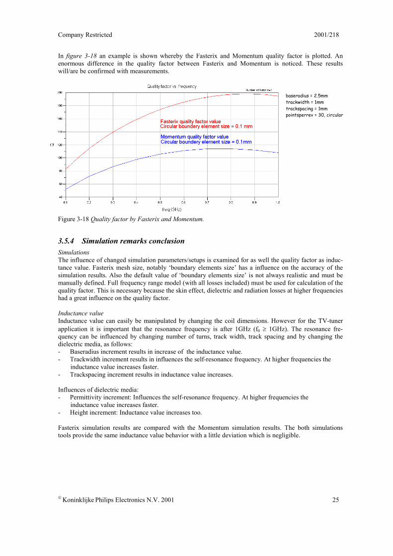
baseradius = 2.5mm trackwidth = 1mm trackspacing = 1mm pointsperrev = 30, circular
Mesh influence on the quality factor is examined for the circular coil. ‘Boundary element size’ has to bemanually defined , because the quality factor is strongly dependant of the skin effect (and skin depth) andbecause the default value does not always represents a realistic b.e.s. In the ‘filename.fasout’ file thedefault ‘boundary element size’ can be viewed.In figure 3-16 an example is shown where the b.e.s. is changed from default value of 0.27mm to 0.1mm.Enormous variation in the quality factor is noticed, as shown in figure 3-16.
3.5.3 Fasterix versus MomentumThe number of mesh elements of Fasterix and Momentum is equated in order to make a simulation resultcomparison. In figure 3-17 an example is shown whereby the Fasterix and Momentum inductance value isplotted. Deviation in the inductance value is negligible. Fasterix and Momentum give almost same simula-tion results.
Figure 3-16 B.e.s. influence on the quality factor.
Figure 3-17 Inductance value by Fasterix and Momentum.
Company Restricted 2001/218
� Koninklijke Philips Electronics N.V. 2001 25
baseradius = 2.5mm trackwidth = 1mm trackspacing = 1mm pointsperrev = 30, circular
In figure 3-18 an example is shown whereby the Fasterix and Momentum quality factor is plotted. Anenormous difference in the quality factor between Fasterix and Momentum is noticed. These resultswill/are be confirmed with measurements.
3.5.4 Simulation remarks conclusionSimulationsThe influence of changed simulation parameters/setups is examined for as well the quality factor as induc-tance value. Fasterix mesh size, notably ‘boundary elements size’ has a influence on the accuracy of thesimulation results. Also the default value of ‘boundary elements size’ is not always realistic and must bemanually defined. Full frequency range model (with all losses included) must be used for calculation of thequality factor. This is necessary because the skin effect, dielectric and radiation losses at higher frequencieshad a great influence on the quality factor.
Inductance valueInductance value can easily be manipulated by changing the coil dimensions. However for the TV-tunerapplication it is important that the resonance frequency is after 1GHz (f0 � 1GHz). The resonance fre-quency can be influenced by changing number of turns, track width, track spacing and by changing thedielectric media, as follows:- Baseradius increment results in increase of the inductance value.- Trackwidth increment results in influences the self-resonance frequency. At higher frequencies the
inductance value increases faster.- Trackspacing increment results in inductance value increases.
Influences of dielectric media:- Permittivity increment: Influences the self-resonance frequency. At higher frequencies the
inductance value increases faster.- Height increment: Inductance value increases too.
Fasterix simulation results are compared with the Momentum simulation results. The both simulationstools provide the same inductance value behavior with a little deviation which is negligible.
Figure 3-18 Quality factor by Fasterix and Momentum.

2001/218 Company Restricted
26 �Koninklijke Philips Electronics N.V. 2001
Quality factorFirst simulations of the quality factor provided an unrealistic values (Q>3000) beacause the High fre-quency range model is used. Full model makes posible to include losses and the more realistic values aresimulated (Q>100). The influences of changed coil dimentions on the quality factor are also examined andare as follow:- Baseradius increment results in more curved line and a little changes in value.- Trackwidth results in a little influence on the quality factor.- Trackspacing increment results in qualtity factor decrease, at higher frequencies .
Influences of dielectric media:- Permittivity increment results in quality factor decrease.- Height increment results in quality factor decrease.
Influence of vias:- Decrease of quality factor when vias are used- ‘Via Lout’ has no influence
Fasterix simulation results are compared with the Momentum simulation results. The results are not corre-sponding which is probably caused by difference in the mesh algorithm. However a curve behaviors aresimilar to each other and an approximation of the quality factor behavior is achieved.
Company Restricted 2001/218
� Koninklijke Philips Electronics N.V. 2001 27
4 Designed coilsOne of the tasks is to measure coils and compare the measurement results with the simulations results.The simulation and measurement layouts are the same. This is done to have the same environment forsimulation as well as measurements.
Measurements of the inductance value and quality factor are done with an LCR-meter. The coil cannot befitted directly to the LCR-meter, therefore a connector and a microstrip are needed for an accurate meas-urements. The measurements are layout dependent, it is important that the influence of the design on themeasurements should be reduced to a minimum.Problems expected with a layout:
- Influence of microstrip on inductance value of a coil- Current distortion at transition connector and microstrip- Current distortion at transition microstrip and coil- Influence of groundplane on quality factor and inductance- Determine electrical length of microstrip
First simulations and measurements are done using ‘Layout design One’ (figure 4-1). These measurementsand simulations are done to understand the influence of shape, trackwidth and groundplane around a coil,on the inductance value.At first it did not seem possible to simulate the realistic quality factor. That is why the quality factor wasonly measured. Later on it was possible to simulate the quality factor, but ‘Layout design One’ influencethe measurements and therefore it wasn’t simulated afterwards because of the reasons mentioned in chap-ter 3.4.Because the simulated and measured inductance value had a non-acceptable deviation, two steps weretaken to find out what the cause could be:- Another simulation program (Momentum) was used to simulate the inductance value- Another layout was made to reduce the influence of the layout on the measurement
To reduce the influence of the layout on measurements another layout was made. With this design, ‘Lay-out design Two’ (figure 4-2), the influence of the number of turns on inductance value and quality factorwas examined.
Figure 4-1 Layout design One
Figure 4-2 Layout design Two
2001/218 Company Restricted
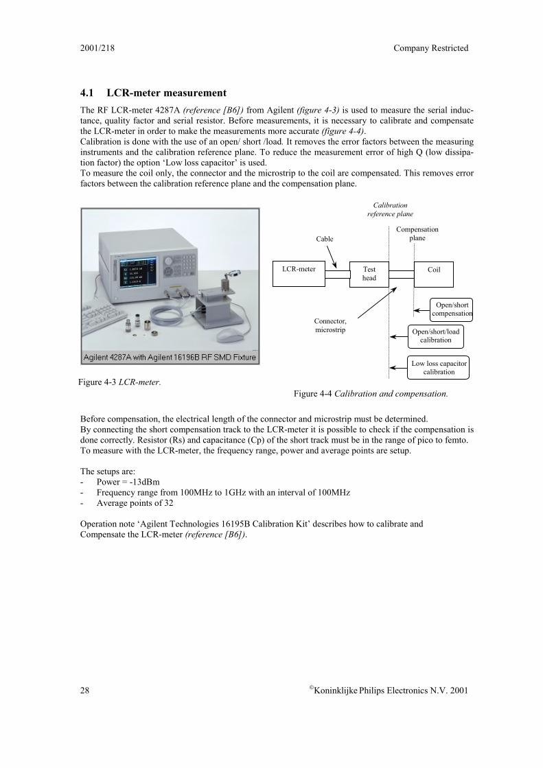
4.1 LCR-meter measurementThe RF LCR-meter 4287A (reference [B6]) from Agilent (figure 4-3) is used to measure the serial induc-tance, quality factor and serial resistor. Before measurements, it is necessary to calibrate and compensatethe LCR-meter in order to make the measurements more accurate (figure 4-4).Calibration is done with the use of an open/ short /load. It removes the error factors between the measuringinstruments and the calibration reference plane. To reduce the measurement error of high Q (low dissipa-tion factor) the option ‘Low loss capacitor’ is used.To measure the coil only, the connector and the microstrip to the coil are compensated. This removes errorfactors between the calibration reference plane and the compensation plane.
Calibrationreference plane
28 �Koninklijke Philips Electronics N.V. 2001
Before compensation, the electrical length of the connector and microstrip must be determined.By connecting the short compensation track to the LCR-meter it is possible to check if the compensation isdone correctly. Resistor (Rs) and capacitance (Cp) of the short track must be in the range of pico to femto.To measure with the LCR-meter, the frequency range, power and average points are setup.
The setups are:- Power = -13dBm- Frequency range from 100MHz to 1GHz with an interval of 100MHz- Average points of 32
Operation note ‘Agilent Technologies 16195B Calibration Kit’ describes how to calibrate andCompensate the LCR-meter (reference [B6]).
Figure 4-3 LCR-meter.Figure 4-4 Calibration and compensation.
LCR-meter Testhead
Coil
Cable
Connector,microstrip
Compensationplane
Open/shortcompensation
Open/short/loadcalibration
Low loss capacitorcalibration
Company Restricted 2001/218
� Koninklijke Philips Electronics N.V. 2001 29
Name Shape coil Remarks L[nH]
Baseradius(mm)
Trackwidth(mm)
Trackspacing(mm)
Number ofturns
Sample 1 Rectangular Drawn withoutFortan program
6 0 1 0.4 1
Sample 2 Octagonal 6 1 0.6 0.5 0.92Sample 3 Octagonal 5 2 1 1 .5Sample 4 Octagonal No groundplane
around coil5 2 1 1 .5
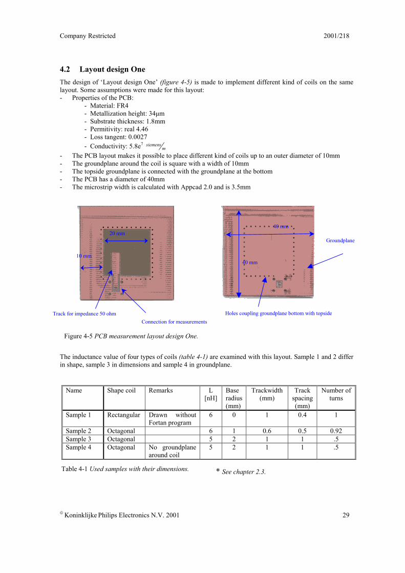
4.2 Layout design OneThe design of ‘Layout design One’ (figure 4-5) is made to implement different kind of coils on the samelayout. Some assumptions were made for this layout:- Properties of the PCB:
- Material: FR4- Metallization height: 34µm- Substrate thickness: 1.8mm- Permitivity: real 4.46- Loss tangent: 0.0027- Conductivity: 5.8e7 m
siemens
- The PCB layout makes it possible to place different kind of coils up to an outer diameter of 10mm- The groundplane around the coil is square with a width of 10mm- The topside groundplane is connected with the groundplane at the bottom- The PCB has a diameter of 40mm- The microstrip width is calculated with Appcad 2.0 and is 3.5mm
The inductance value of four types of coils (table 4-1) are examined with this layout. Sample 1 and 2 differin shape, sample 3 in dimensions and sample 4 in groundplane.
Figure 4-5 PCB measurement layout design One.
Table 4-1 Used samples with their dimensions.
Groundplane
Track for impedance 50 ohmConnection for measurements
20 mm
10 mm
Holes coupling groundplane bottom with topside
40 mm
40 mm
* See chapter 2.3.
2001/218 Company Restricted
30 �Koninklijke Philips Electronics N.V. 2001
5.00
6.00
7.00
8.00
9.00
10.00
11.00
100 200 300 400 500 600 700 800 900 1000freq [MHz]
L [n
H]
sample 1 (meas) sample 2 (meas) sample 1 (sim)sample 2 (sim)
4.00
4.50
5.00
5.50
6.00
6.50
7.00
100 200 300 400 500 600 700 800 900 1000
freq [MHz]
L [n
H]
sample 3 (meas) sample 4 (meas) sample 3 (sim)sample 4 (sim)
0
100
200
300
400
500
600
1 10 100 200 300 400 500 600 700 800 900 1000freq [MHz]
Q
sample 1 (meas) sample 2 (meas) sample 3 (meas) sample 4 (meas)
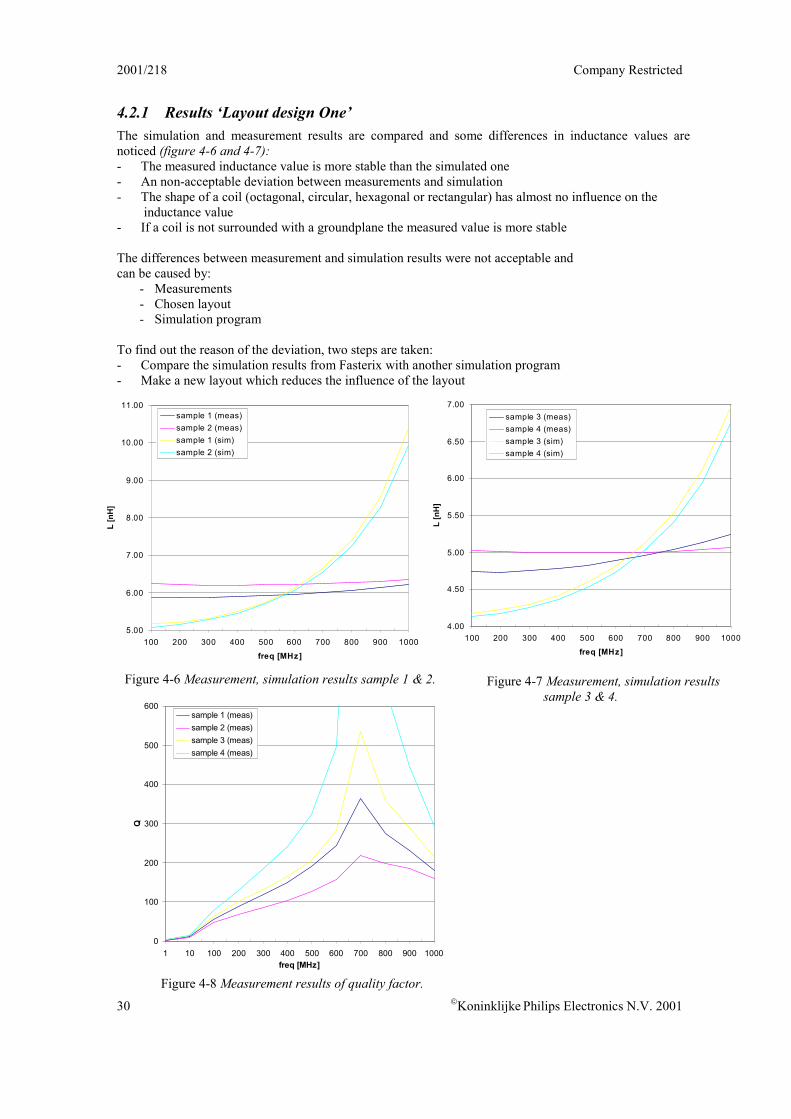
4.2.1 Results ‘Layout design One’The simulation and measurement results are compared and some differences in inductance values arenoticed (figure 4-6 and 4-7):- The measured inductance value is more stable than the simulated one- An non-acceptable deviation between measurements and simulation- The shape of a coil (octagonal, circular, hexagonal or rectangular) has almost no influence on the inductance value- If a coil is not surrounded with a groundplane the measured value is more stable
The differences between measurement and simulation results were not acceptable andcan be caused by:
- Measurements- Chosen layout- Simulation program
To find out the reason of the deviation, two steps are taken:- Compare the simulation results from Fasterix with another simulation program- Make a new layout which reduces the influence of the layout
Figure 4-6 Measurement, simulation results sample 1 & 2. Figure 4-7 Measurement, simulation resultssample 3 & 4.
Figure 4-8 Measurement results of quality factor.
Company Restricted 2001/218
� Koninklijke Philips Electronics N.V. 2001 31
4.00
4.50
5.00
5.50
6.00
6.50
7.00
7.50
100 200 300 400 500 600 700 800 900 1000
freq [MHz]
L [n
H]
fasterixmomentummeasurement
4.2.2 Fasterix and Momentum comparisonMomentum is another simulation tool used to set up and perform electromagnetic simulations on passive,planar circuits. Because the deviation between measurement and Fasterix simulation results of ‘Layoutdesign One’ was not acceptable, a simulation comparison between Momentum and Fasterix is done. Theresults of inductance values in Momentum complied with those from Fasterix (figure 4-9).
With this knowledge, it can be concluded Fasterix does not cause the difference between measurement andsimulation.
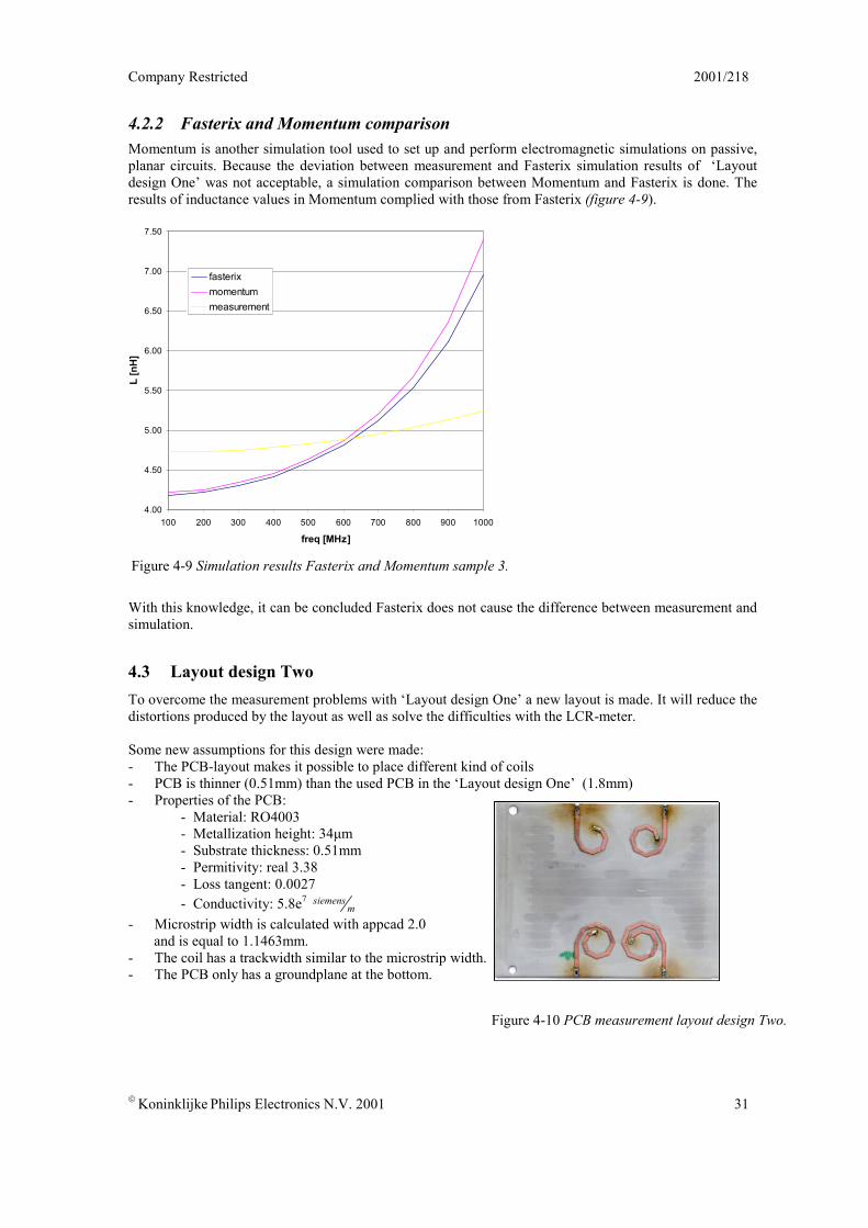
4.3 Layout design TwoTo overcome the measurement problems with ‘Layout design One’ a new layout is made. It will reduce thedistortions produced by the layout as well as solve the difficulties with the LCR-meter.
Some new assumptions for this design were made:- The PCB-layout makes it possible to place different kind of coils- PCB is thinner (0.51mm) than the used PCB in the ‘Layout design One’ (1.8mm)- Properties of the PCB:
- Material: RO4003- Metallization height: 34µm- Substrate thickness: 0.51mm- Permitivity: real 3.38- Loss tangent: 0.0027- Conductivity: 5.8e7 m
siemens
- Microstrip width is calculated with appcad 2.0 and is equal to 1.1463mm.- The coil has a trackwidth similar to the microstrip width.- The PCB only has a groundplane at the bottom.
Figure 4-9 Simulation results Fasterix and Momentum sample 3.
Figure 4-10 PCB measurement layout design Two.
2001/218 Company Restricted
32 �Koninklijke Philips Electronics N.V. 2001
-350
-300
-250
-200
-150
-100
-50
0
50
100
100 200 300 400 500 600 700 800 900 1000
f [MHz]
L[nH
]
0.75 Turn 1.00 Turn 1.25 Turn 1.50 Turn 0
5
10
15
20
25
30
100 300 500 700 900f [MHz]
L [n
H]
0.75 Turn1.00 Turn1.25 Turn
0
50
100
150
200
250
100 300 500 700 900f [MHz]
Q
0,75 Turn1.00 Turn1.25 Turn1.50 Turn
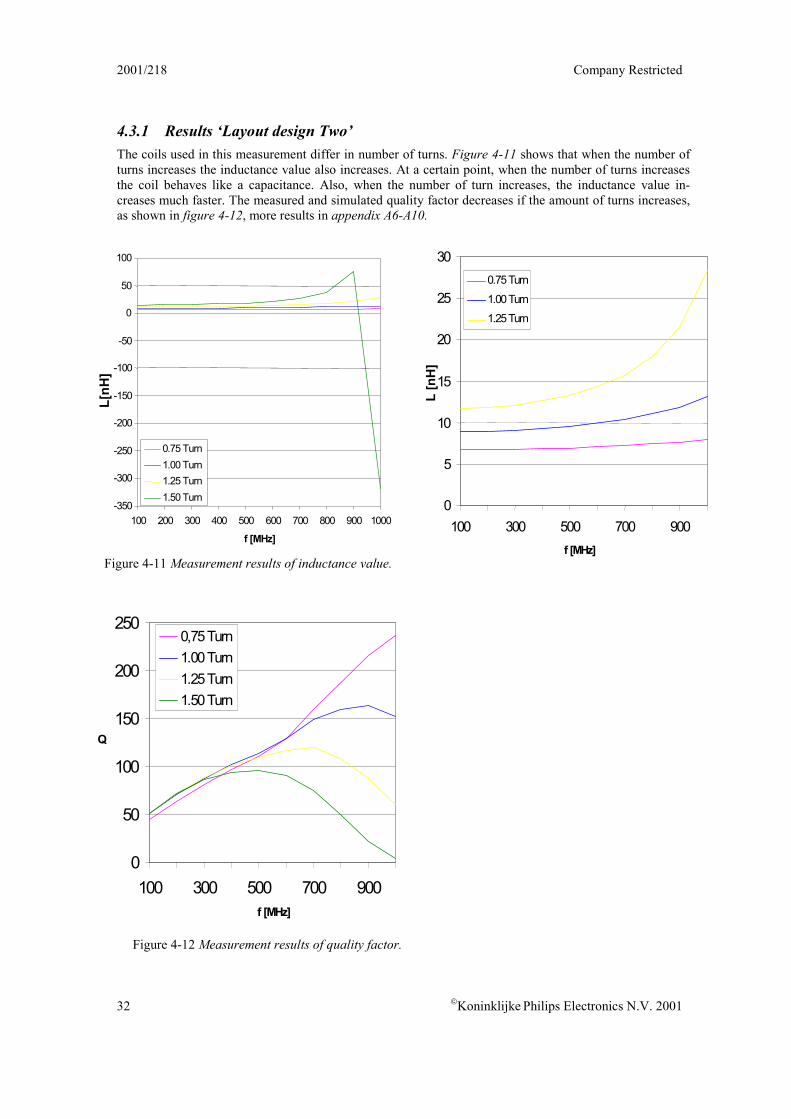
4.3.1 Results ‘Layout design Two’The coils used in this measurement differ in number of turns. Figure 4-11 shows that when the number ofturns increases the inductance value also increases. At a certain point, when the number of turns increasesthe coil behaves like a capacitance. Also, when the number of turn increases, the inductance value in-creases much faster. The measured and simulated quality factor decreases if the amount of turns increases,as shown in figure 4-12, more results in appendix A6-A10.
Figure 4-11 Measurement results of inductance value.
Figure 4-12 Measurement results of quality factor.
Company Restricted 2001/218
� Koninklijke Philips Electronics N.V. 2001 33
0
2
4
6
8
10
12
14
16
100 200 300 400 500 600 700 800 900 100f [MHz]
L [n
H]
MeasureSimulate
0
0.1
0.2
0.3
0.4
0.5
0.6
0.7
0.8
0.9
100 200 300 400 500 600 700 800 900 100f [MHz]
Rs
[ohm
]
MeasureSimulate
0
20
40
60
80
100 120
140
160
180
100 200 300 400 500 600 700 800 900 1000
f [MHz]
Q
MeasuredSimulated
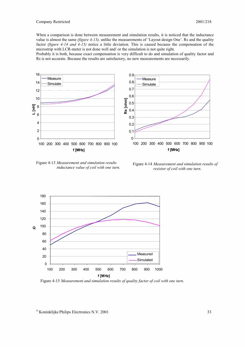
When a comparison is done between measurement and simulation results, it is noticed that the inductancevalue is almost the same (figure 4-13), unlike the measurements of ‘Layout design One’. Rs and the qualityfactor (figure 4-14 and 4-15) notice a little deviation. This is caused because the compensation of themicrostrip with LCR-meter is not done well and/ or the simulation is not quite right.Probably it is both, because exact compensation is very difficult to do and simulation of quality factor andRs is not accurate. Because the results are satisfactory, no new measurements are necessarily.
Figure 4-13 Measurement and simulation resultsinductance value of coil with one turn.
Figure 4-14 Measurement and simulation results ofresistor of coil with one turn.
Figure 4-15 Measurement and simulation results of quality factor of coil with one turn.
2001/218 Company Restricted
34 �Koninklijke Philips Electronics N.V. 2001
4.4 Designed coils conclusionIf a coil is measured, it is important to use a layout that has almost no influence on the measurements.‘Layout design One’ has an influence on the measurements.This is caused by:ϑ Current distortion at end of microstrip because microstrip width is wider than coilwidthϑ Microstrip is near coil. This can influence the induction of the coil.ϑ Connection of LCR-meter is vertical on PCB. This give reflection on the transition
These problems are solved when using ‘Layout design Two’. Measurements and simulations results has anacceptable deviation.If the number of turns increases, the inductance value increases too. At a certain point the coil behaves likea capacitance. This is due to the self-resonance frequency of the coil, which is a unwanted behavior. Whendesigning coils, take the frequency range used for the coil into consideration.
The spiral shape has almost no influence on the inductance value. The groundplane surrounding the coil onboth top- and bottomside has almost no influence on the inductance value, but it will influence the qualityfactor of a coil. This is because a groundplane or other tracks nearby the coil will create a parasitic capaci-tance, which has a negative effect on the quality factor.
The simulation tool Fasterix can be used to simulate coils, it gives a good representation of the behavior ofa PCB coil.
Company Restricted 2001/218
� Koninklijke Philips Electronics N.V. 2001 35
5 Circuit implementationThe simulation and measurements of single coil did correspond. This conclusion is necessary for thefurther simulations with Fasterix. The air-coils that are used in the tracking filter circuit have to be replacedwith coils on PCB. Implementing a coil in a circuit will have a great influence on the quality factor. Thequality factor will lower because of the extra introduced losses. This is caused by other layer materialsituated nearby the coil, which increase the parasitic capacitance of the inductor.
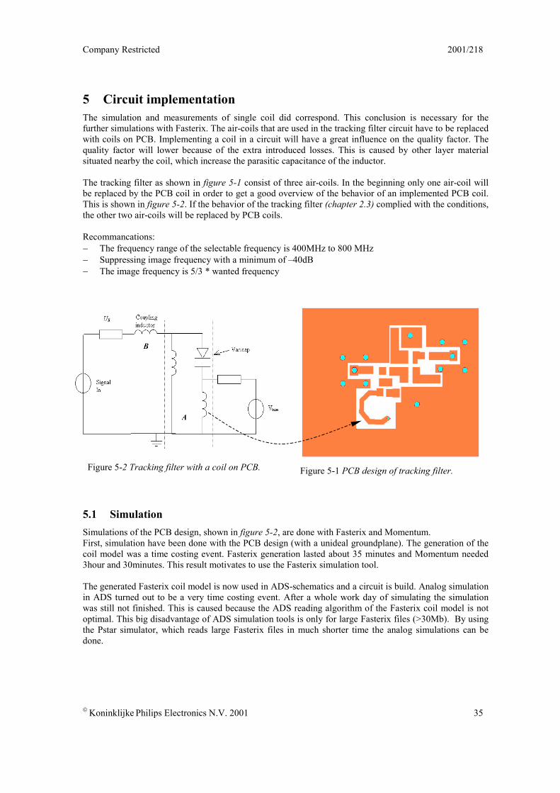
The tracking filter as shown in figure 5-1 consist of three air-coils. In the beginning only one air-coil willbe replaced by the PCB coil in order to get a good overview of the behavior of an implemented PCB coil.This is shown in figure 5-2. If the behavior of the tracking filter (chapter 2.3) complied with the conditions,the other two air-coils will be replaced by PCB coils.
Recommancations:ϑ The frequency range of the selectable frequency is 400MHz to 800 MHzϑ Suppressing image frequency with a minimum of –40dBϑ The image frequency is 5/3 * wanted frequency
5.1 SimulationSimulations of the PCB design, shown in figure 5-2, are done with Fasterix and Momentum.First, simulation have been done with the PCB design (with a unideal groundplane). The generation of thecoil model was a time costing event. Fasterix generation lasted about 35 minutes and Momentum needed3hour and 30minutes. This result motivates to use the Fasterix simulation tool.
The generated Fasterix coil model is now used in ADS-schematics and a circuit is build. Analog simulationin ADS turned out to be a very time costing event. After a whole work day of simulating the simulationwas still not finished. This is caused because the ADS reading algorithm of the Fasterix coil model is notoptimal. This big disadvantage of ADS simulation tools is only for large Fasterix files (>30Mb). By usingthe Pstar simulator, which reads large Fasterix files in much shorter time the analog simulations can bedone.
Figure 5-1 PCB design of tracking filter.Figure 5-2 Tracking filter with a coil on PCB.
2001/218 Company Restricted
36 �Koninklijke Philips Electronics N.V. 2001
Normal layout Coil milled Coil and ground-
plane
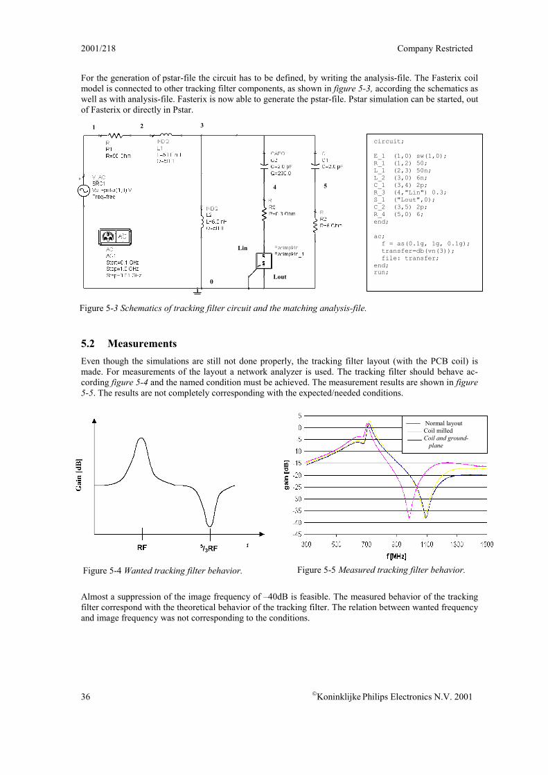
For the generation of pstar-file the circuit has to be defined, by writing the analysis-file. The Fasterix coilmodel is connected to other tracking filter components, as shown in figure 5-3, according the schematics aswell as with analysis-file. Fasterix is now able to generate the pstar-file. Pstar simulation can be started, outof Fasterix or directly in Pstar.
5.2 MeasurementsEven though the simulations are still not done properly, the tracking filter layout (with the PCB coil) ismade. For measurements of the layout a network analyzer is used. The tracking filter should behave ac-cording figure 5-4 and the named condition must be achieved. The measurement results are shown in figure5-5. The results are not completely corresponding with the expected/needed conditions.
Almost a suppression of the image frequency of –40dB is feasible. The measured behavior of the trackingfilter correspond with the theoretical behavior of the tracking filter. The relation between wanted frequencyand image frequency was not corresponding to the conditions.
Figure 5-3 Schematics of tracking filter circuit and the matching analysis-file.
Figure 5-4 Wanted tracking filter behavior. Figure 5-5 Measured tracking filter behavior.
circuit;
E_1 (1,0) sw(1,0);R_1 (1,2) 50;L_1 (2,3) 50n;L_2 (3,0) 6n;C_1 (3,4) 2p;R_3 (4,"Lin") 0.3;S_1 ("Lout",0);C_2 (3,5) 2p;R_4 (5,0) 6;end;
ac; f = as(0.1g, 1g, 0.1g); transfer=db(vn(3)); file: transfer;end;run;
Lin
1 2 3
4
Lout
5
0
Company Restricted 2001/218
� Koninklijke Philips Electronics N.V. 2001 37
-60
-50
-40
-30
-20
-10
0
10
300 500 700 900 1100 1300 1500
f [MHz]
gain
[dB
]
-60
-50
-40
-30
-20
-10
0
10
300 500 700 900 1100 1300 1500
f [MHz]
gain
[dB
]
Vtune = 5V
Vtune = 10V
Vtune = 15V
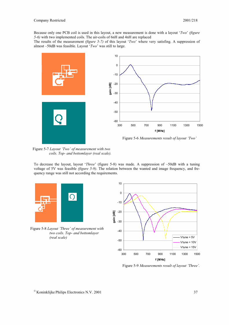
Because only one PCB coil is used in this layout, a new measurement is done with a layout ‘Two’ (figure5-6) with two implemented coils. The air-coils of 6nH and 4nH are replacedThe results of the measurement (figure 5-7) of this layout ‘Two’ where very satisfing. A suppression ofalmost –50dB was feasible. Layout ‘Two’ was still to large.
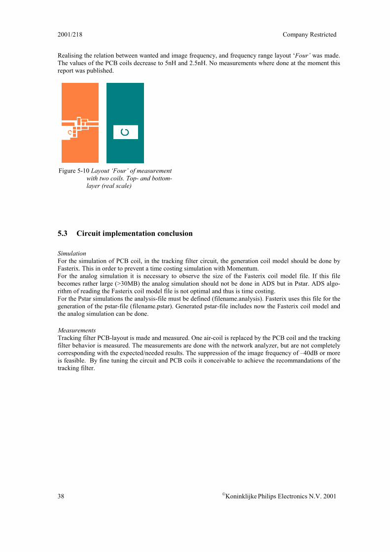
To decrease the layout, layout ‘Three’ (figure 5-8) was made. A suppression of –50dB with a tuningvoltage of 5V was feasible (figure 5-9). The relation between the wanted and image frequency, and fre-quency range was still not according the requirements.
Figure 5-6 Measurements result of layout ‘Two’
Figure 5-7 Layout ‘Two’ of measurement with twocoils. Top- and bottomlayer (real scale).
Figure 5-8 Layout ’Three’ of measurement withtwo coils. Top- and bottomlayer(real scale)
Figure 5-9 Measurements result of layout ‘Three’.
2001/218 Company Restricted
38 �Koninklijke Philips Electronics N.V. 2001
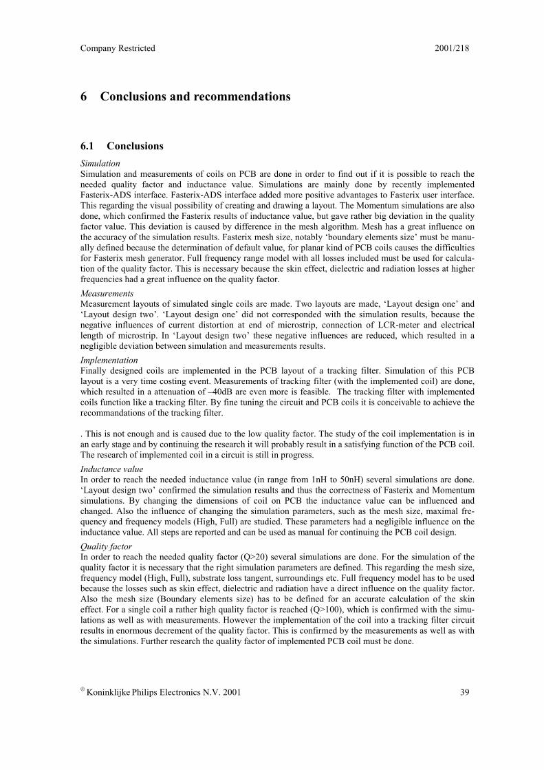
Realising the relation between wanted and image frequency, and frequency range layout ‘Four’ was made.The values of the PCB coils decrease to 5nH and 2.5nH. No measurements where done at the moment thisreport was published.
5.3 Circuit implementation conclusion
SimulationFor the simulation of PCB coil, in the tracking filter circuit, the generation coil model should be done byFasterix. This in order to prevent a time costing simulation with Momentum.For the analog simulation it is necessary to observe the size of the Fasterix coil model file. If this filebecomes rather large (>30MB) the analog simulation should not be done in ADS but in Pstar. ADS algo-rithm of reading the Fasterix coil model file is not optimal and thus is time costing.For the Pstar simulations the analysis-file must be defined (filename.analysis). Fasterix uses this file for thegeneration of the pstar-file (filename.pstar). Generated pstar-file includes now the Fasterix coil model andthe analog simulation can be done.
MeasurementsTracking filter PCB-layout is made and measured. One air-coil is replaced by the PCB coil and the trackingfilter behavior is measured. The measurements are done with the network analyzer, but are not completelycorresponding with the expected/needed results. The suppression of the image frequency of –40dB or moreis feasible. By fine tuning the circuit and PCB coils it conceivable to achieve the recommandations of thetracking filter.
Figure 5-10 Layout ‘Four’ of measurementwith two coils. Top- and bottom-layer (real scale)
Company Restricted 2001/218
� Koninklijke Philips Electronics N.V. 2001 39
6 Conclusions and recommendations
6.1 ConclusionsSimulationSimulation and measurements of coils on PCB are done in order to find out if it is possible to reach theneeded quality factor and inductance value. Simulations are mainly done by recently implementedFasterix-ADS interface. Fasterix-ADS interface added more positive advantages to Fasterix user interface.This regarding the visual possibility of creating and drawing a layout. The Momentum simulations are alsodone, which confirmed the Fasterix results of inductance value, but gave rather big deviation in the qualityfactor value. This deviation is caused by difference in the mesh algorithm. Mesh has a great influence onthe accuracy of the simulation results. Fasterix mesh size, notably ‘boundary elements size’ must be manu-ally defined because the determination of default value, for planar kind of PCB coils causes the difficultiesfor Fasterix mesh generator. Full frequency range model with all losses included must be used for calcula-tion of the quality factor. This is necessary because the skin effect, dielectric and radiation losses at higherfrequencies had a great influence on the quality factor.MeasurementsMeasurement layouts of simulated single coils are made. Two layouts are made, ‘Layout design one’ and‘Layout design two’. ‘Layout design one’ did not corresponded with the simulation results, because thenegative influences of current distortion at end of microstrip, connection of LCR-meter and electricallength of microstrip. In ‘Layout design two’ these negative influences are reduced, which resulted in anegligible deviation between simulation and measurements results.ImplementationFinally designed coils are implemented in the PCB layout of a tracking filter. Simulation of this PCBlayout is a very time costing event. Measurements of tracking filter (with the implemented coil) are done,which resulted in a attenuation of –40dB are even more is feasible. The tracking filter with implementedcoils function like a tracking filter. By fine tuning the circuit and PCB coils it is conceivable to achieve therecommandations of the tracking filter.
. This is not enough and is caused due to the low quality factor. The study of the coil implementation is inan early stage and by continuing the research it will probably result in a satisfying function of the PCB coil.The research of implemented coil in a circuit is still in progress.Inductance valueIn order to reach the needed inductance value (in range from 1nH to 50nH) several simulations are done.‘Layout design two’ confirmed the simulation results and thus the correctness of Fasterix and Momentumsimulations. By changing the dimensions of coil on PCB the inductance value can be influenced andchanged. Also the influence of changing the simulation parameters, such as the mesh size, maximal fre-quency and frequency models (High, Full) are studied. These parameters had a negligible influence on theinductance value. All steps are reported and can be used as manual for continuing the PCB coil design.Quality factorIn order to reach the needed quality factor (Q>20) several simulations are done. For the simulation of thequality factor it is necessary that the right simulation parameters are defined. This regarding the mesh size,frequency model (High, Full), substrate loss tangent, surroundings etc. Full frequency model has to be usedbecause the losses such as skin effect, dielectric and radiation have a direct influence on the quality factor.Also the mesh size (Boundary elements size) has to be defined for an accurate calculation of the skineffect. For a single coil a rather high quality factor is reached (Q>100), which is confirmed with the simu-lations as well as with measurements. However the implementation of the coil into a tracking filter circuitresults in enormous decrement of the quality factor. This is confirmed by the measurements as well as withthe simulations. Further research the quality factor of implemented PCB coil must be done.
2001/218 Company Restricted
40 �Koninklijke Philips Electronics N.V. 2001
6.2 Recommendations
SimulationSimulation of PCB coil can be time costing if the setups are not done properly. This documents representsall necessary setups that will lead to accurate Fasterix simulation results.Preparation of the layout data in the ADS-Layout window is limited considering the spiral coils shapes.This is a reason that for a design of the layout data the Fortran program must be used. This program allowsthe user to crate a complex coil shape in short time.Considering the simulations of designed coil it is important that the Full frequency range model is usedbecause of the possibility of including the losses. Also an important simulation parameters is the mesh.Fasterix mesh algorithm is not always optimal for irregular coil shapes and if not observed can lead tosystem crash. Thus the number of mesh elements must be observed and if it exceeds the expected value thecoil layout has to be redrawn or rotated. Determination of default value of ‘boundary elements size’ mustbe manually defined. ‘Boundary elements size’ defines the skin depth and thus the accuracy of the qualityfactor value. However if this value is equated to the skin depth it will possibly lead to system crash.‘Boundary element size’ should have the value of one tenth of the track width which will prevent theunwanted Fasterix behavior or possible system crash. Changes in the Fasterix mesh algorithm will proba-bly solve this problem.Momentum simulation tool can be useful for the comparison of the Fasterix simulation results. However ifthe layout size increases Momentum needs more simulation time then Fasterix. In case of implementationof PCB coil in tracking filter layout Fasterix generated a large files (filesize > 30Mb). Because of nonoptimal ADS-Schematic algorithm for reading the Fasterix file, it costs to much time to simulate the analogbehavior of the coil model. In this cases the analog simulation of the Fasterix coil model should be done inPstar.MeasurementsFor the corresponding simulation and measurements results the correct layout design is necessary. Thewidth of the impedance track should be equal to the width of the coil track. This will prevent unwantedcurrent distortion. Also the correct calibration of the LCR-meter is necessary.ImplementationLayout design should be as optimal as possible. This regarding the parasitic capacitance and other losses.This can be achieved by solid connection to the groundplane and small distance between component/tracksand the groundplane.Inductance valueInductance value can easily be realized. This document provides the insight into the inductance valuebehavior versus the changing of coil dimensions.Quality factorImplemented coil results in a lower quality factor. Main idea is to optimise the PCD design, meaning thatthe parasitic capacitance is as low as possible. In order to increase quality factor the other possibilities mustbe studied. For example, removing the groundplane underneath the coil can result in higher quality factor.Possibility of two parallel coils on PCB and its influence on the quality factor has to be examined. For allthese possibility the Fasterix simulation tool can be used, whereby the Full frequency range (all lossesincluded) is necessary for a realistic approximation of quality factor.
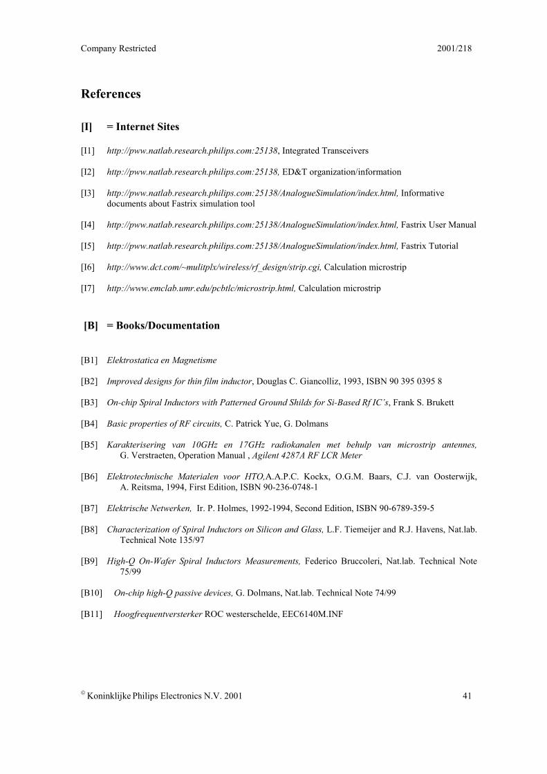
Company Restricted 2001/218
� Koninklijke Philips Electronics N.V. 2001 41
References
[I] = Internet Sites
[I1] http://pww.natlab.research.philips.com:25138, Integrated Transceivers
[I2] http://pww.natlab.research.philips.com:25138, ED&T organization/information
[I3] http://pww.natlab.research.philips.com:25138/AnalogueSimulation/index.html, Informativedocuments about Fastrix simulation tool
[I4] http://pww.natlab.research.philips.com:25138/AnalogueSimulation/index.html, Fastrix User Manual
[I5] http://pww.natlab.research.philips.com:25138/AnalogueSimulation/index.html, Fastrix Tutorial
[I6] http://www.dct.com/~mulitplx/wireless/rf_design/strip.cgi, Calculation microstrip
[I7] http://www.emclab.umr.edu/pcbtlc/microstrip.html, Calculation microstrip
[B] = Books/Documentation
[B1] Elektrostatica en Magnetisme
[B2] Improved designs for thin film inductor, Douglas C. Giancolliz, 1993, ISBN 90 395 0395 8
[B3] On-chip Spiral Inductors with Patterned Ground Shilds for Si-Based Rf IC’s, Frank S. Brukett
[B4] Basic properties of RF circuits, C. Patrick Yue, G. Dolmans
[B5] Karakterisering van 10GHz en 17GHz radiokanalen met behulp van microstrip antennes,G. Verstraeten, Operation Manual , Agilent 4287A RF LCR Meter
[B6] Elektrotechnische Materialen voor HTO,A.A.P.C. Kockx, O.G.M. Baars, C.J. van Oosterwijk,A. Reitsma, 1994, First Edition, ISBN 90-236-0748-1
[B7] Elektrische Netwerken, Ir. P. Holmes, 1992-1994, Second Edition, ISBN 90-6789-359-5
[B8] Characterization of Spiral Inductors on Silicon and Glass, L.F. Tiemeijer and R.J. Havens, Nat.lab.Technical Note 135/97
[B9] High-Q On-Wafer Spiral Inductors Measurements, Federico Bruccoleri, Nat.lab. Technical Note75/99
[B10] On-chip high-Q passive devices, G. Dolmans, Nat.lab. Technical Note 74/99
[B11] Hoogfrequentversterker ROC westerschelde, EEC6140M.INF
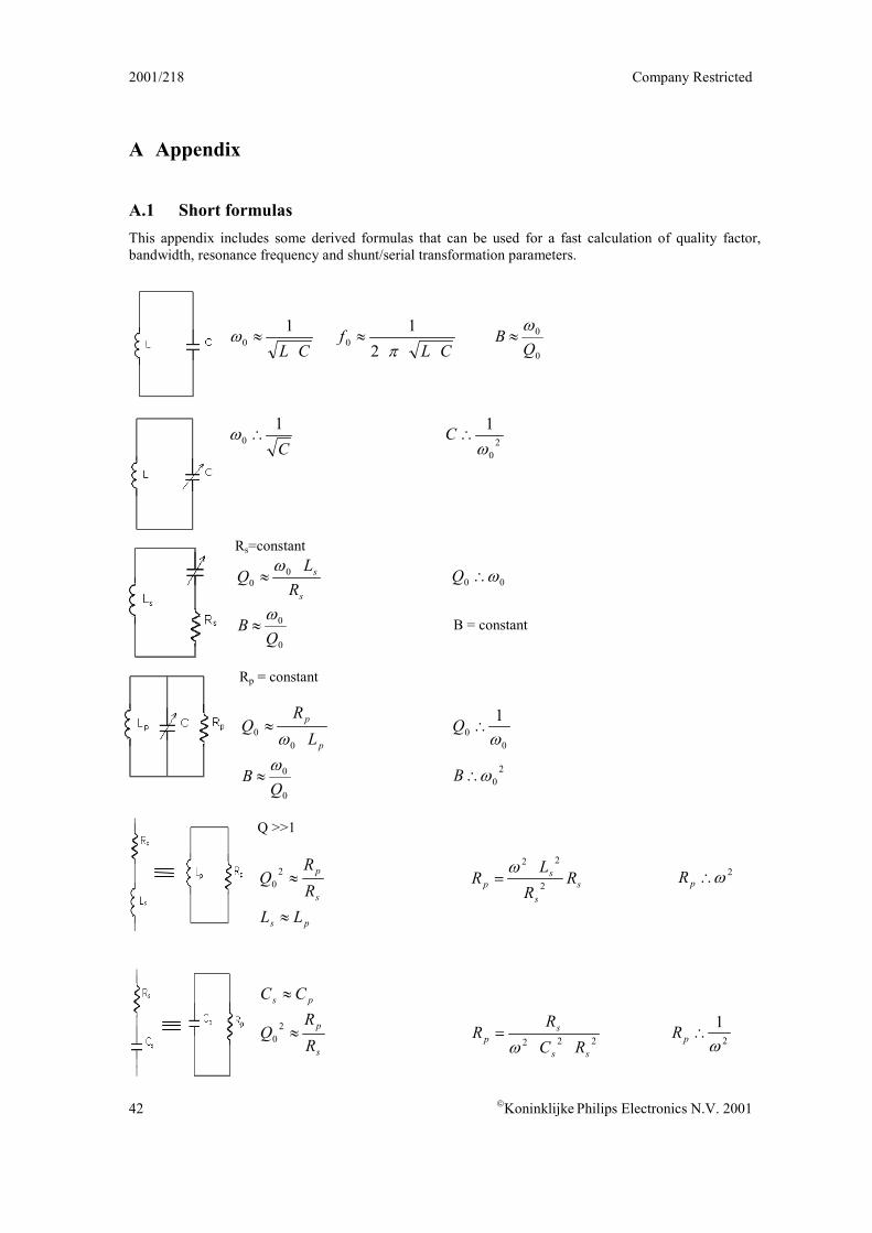
2001/218 Company Restricted
42 �Koninklijke Philips Electronics N.V. 2001
A Appendix
A.1 Short formulasThis appendix includes some derived formulas that can be used for a fast calculation of quality factor,bandwidth, resonance frequency and shunt/serial transformation parameters.
CL�
10∂
CLf �
↓21
00
0
QB
∂
C1
0 ψ∂ 2
0
1∂
ψC
Rs=constant
s
s
RL
Q �0
0∂
00 ∂ψQ
0
0
QB
∂
B = constant
Rp = constant
p
p
LR
Q �
00
∂ 00
1∂
ψQ
0
0
QB
∂
20∂ψB
Q >>1
s
p
RR
Q 2
0 ss
sp R
RL
R 2
22
_
∂
2∂ψpR
ps LL
ps CC
s
p
RR
Q 2
0 222
ss
sp RC
RR _
∂
2
1∂
ψpR
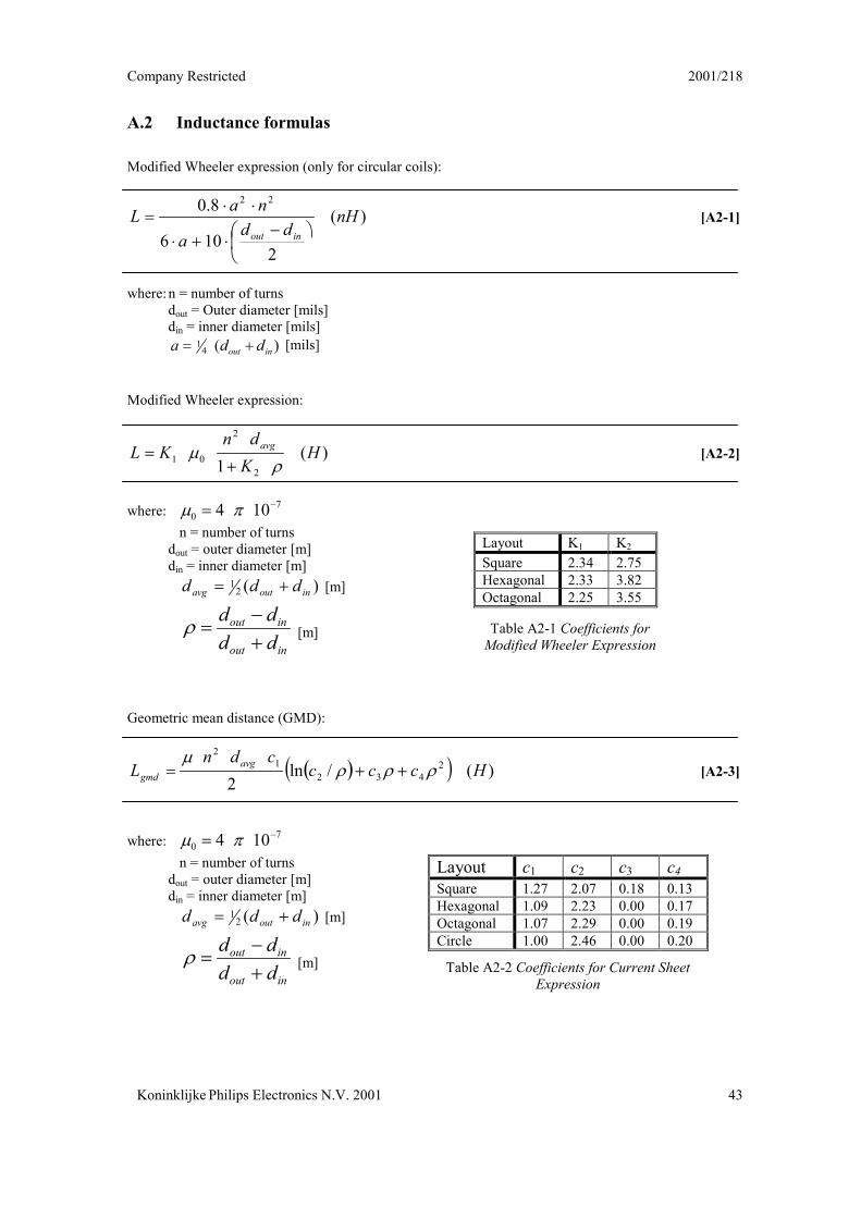
Company Restricted 2001/218
Koninklijke Philips Electronics N.V. 2001
A.2 Inductance formulas
Modified Wheeler expression (only for circular coils):
)(
2106
8.0 22
nHdda
naLinout �
��
� ς�Τ�
��φ [A2-1]
where:n = number of turnsdout = Outer diameter [mils]din = inner diameter [mils]
)(41
inout dda Η_ [mils]
Modified Wheeler expression:
)(1 2
2
01 HK
dnKL avg
±←
Μ
_ [A2-2]
where: 70 104 ϑ
_ ↓←
n = number of turnsdout = outer diameter [m]din = inner diameter [m]
)(21
inoutavg ddd ΗΖ [m]
inout
inout
dddd
Η
ϑΖ± [m]
Geometric mean distance (GMD):
Ε ΦΕ Φ )(/ln2
2432
12
Hccccdn
L avggmd ±±±
←ΗΗ_ [A2-3]
where: 70 104 ϑ
_ ↓←
n = number of turnsdout = outer diameter [m]din = inner diameter [m]
)(21
inoutavg ddd ΗΖ [m]
inout
inout
dddd
Η
ϑΖ± [m]
Table A2-1 Coefficients forModified Wheeler Expression
Layout K1 K2
Square 2.34 2.75Hexagonal 2.33 3.82Octagonal 2.25 3.55
Layout c1 c2 c3 c4Square 1.27 2.07 0.18 0.13Hexagonal 1.09 2.23 0.00 0.17Octagonal 1.07 2.29 0.00 0.19Circle 1.00 2.46 0.00 0.20
43
Table A2-2 Coefficients for Current SheetExpression
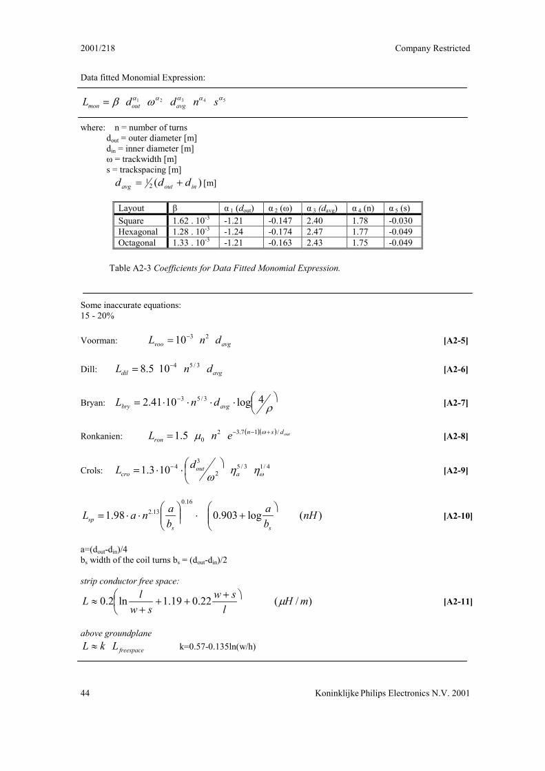
2001/218 Company Restricted
44
Data fitted Monomial Expression:
54321 ∼∼∼∼∼
∂ϒ snddL avgoutmon _
where: n = number of turnsdout = outer diameter [m]din = inner diameter [m]ω = trackwidth [m]s = trackspacing [m]
)(21
inoutavg ddd ΗΖ [m]
Some ina15 - 20%
Voorman
Dill:
Bryan:
Ronkanie
Crols:
.1Lsp φ
a=(dout-dbs width
strip con
2.0L �
above grkL �
T
Layout β α 1 (dout) α 2 (ω) α 3 (davg) α 4 (n) α 5 (s)Square 1.62 . 10-3 -1.21 -0.147 2.40 1.78 -0.030Hexagonal 1.28 . 10-3 -1.24 -0.174 2.47 1.77 -0.049Octagonal 1.33 . 10-3 -1.21 -0.163 2.43 1.75 -0.049
Koninklijke Philips Electronics N.V. 2001
ccurate equations:
: avgvoo dnL _ϑ 2310 [A2-5]
avgdil dnL _ϑ 3/54105.8 [A2-6]
��������φ ϑ
±4log1041.2 3/53
avgbry dnL [A2-7]
n: Ε ΦΕ Φ outdsnron enL /17.32
05.1 Ηϑϑ
_∂
← [A2-8]
4/13/52
34103.1
∂♣♣
∂
���
���φ ϑ
aout
crodL [A2-9]
)(log903.09816.0
13.2 nHba
bana
ss
����
����
����
��� [A2-10]
in)/4of the coil turns bs = (dout-din)/2
ductor free space:
)/(22.019.1ln mHl
swsw
l←
���
� ΤΤΤ
Τ[A2-11]
oundplane
freespaceL k=0.57-0.135ln(w/h)
able A2-3 Coefficients for Data Fitted Monomial Expression.
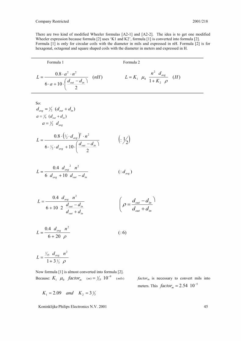
Company Restricted 2001/218
Koninklijke Philips Electronics N.V. 2001
There are two kind of modified Wheeler formulas [A2-1] and [A2-2]. The idea is to get one modifiedWheeler expression because formula [2] uses ‘K1 and K2’, formula [1] is converted into formula [2].Formula [1] is only for circular coils with the diameter in mils and expressed in nH. Formula [2] is forhexagonal, octagonal and square shaped coils with the diameter in meters and expressed in H.
Formula 1 Formula 2
)(
2106
8.0 22
nHdda
naLinout �
��
� ς�Τ�
��φ )(
1 2
2
01 HK
dnKL avg
±←
Μ
_
So:)(2
1inoutavg ddd Η_
)(41
inout dda Η_
avgda _ 21
Ε Φ ΦΕ 21:
2106
8.0
21
222
1
���
� ς�Τ��
���φ
inoutavg
avg
ddd
ndL
):(106
4.0 22
avginoutavg
avg dddd
ndL
ϑΜ
_
inout
inout
avg
dddd
ndL
Μ
ϑ
Μ
_
2106
4.0 2
2064.0 2
±Μ
_
ndL avg
±Μ
_
31
215
1
31nd
L avg
Now formula [1] is almost converted into formulaBecause: )(
915
101 10mmfactorK ϑ
_←
31
21 309.2 ΖΖ KandK
�
45
)6:(
[2].)(mils factorm is necessary to convert mils into
meters. This 51054.2 ϑ
_mfactor
���
�
Τ
ςφ
inout
inout
dddd
±
2001/218 Company Restricted
46 Koninklijke Philips Electronics N.V. 2001
A.3 Something about capacitors
A.3.1 DC-behaviorIn the schematics below is the capacitor connected to a DC-source. At the moment that the switch S isclosed the current IC and the voltage UC behave as given in formula [A5-1].
At the moment when current reaches the maximum value R
UI b
C Ζmax, the voltage UL drops down to a
zero and the coil functions as a shortcut as shown in figure3-1.
����
�ς�φ
Ο
CRt
bC eUU 1�
���
��φ
Ο
CRt
bC e
RUI [A3-1]
A.3.2 AC-behavior
In the schematics below is the capacitor connected to a AC-source. If the AC-source a sinus is then itappears that the iC and uC are also sinus signals with the phase difference of 90 degrees (see figure A3-2).
CZ _
∂
1
dtduCi C
C _ [A3-2]
Figure A3-1 DC-behavior of the currant and voltage across a capacitor.
Figure A5-2 AC-behavior of the current and voltage across a capacitor.
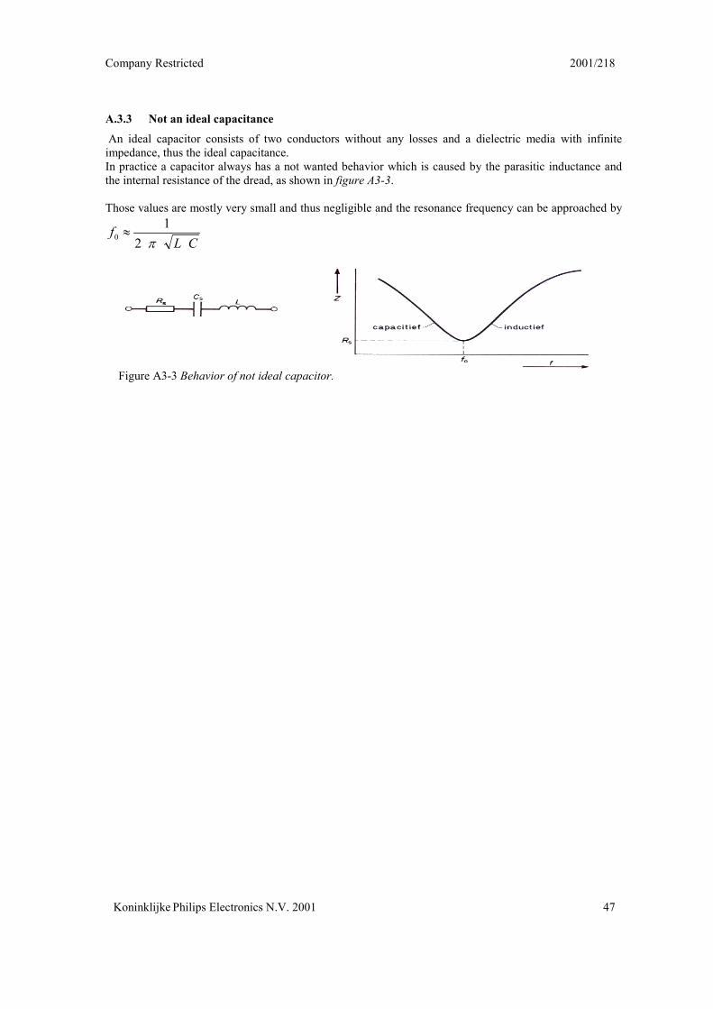
Company Restricted 2001/218
Koninklijke Philips Electronics N.V. 2001 47
A.3.3 Not an ideal capacitance An ideal capacitor consists of two conductors without any losses and a dielectric media with infiniteimpedance, thus the ideal capacitance.In practice a capacitor always has a not wanted behavior which is caused by the parasitic inductance andthe internal resistance of the dread, as shown in figure A3-3.
Those values are mostly very small and thus negligible and the resonance frequency can be approached by
CLf �
↓21
0
Figure A3-3 Behavior of not ideal capacitor.
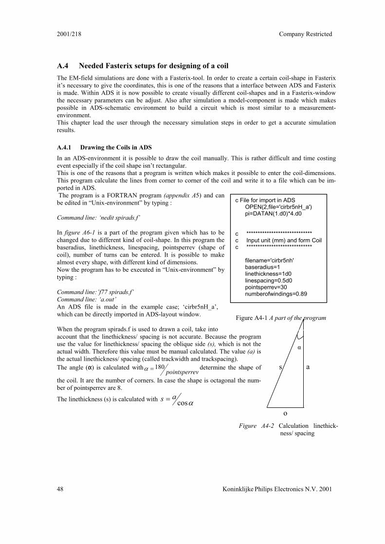
2001/218 Company Restricted
48 Kon
A.4 Needed Fasterix setups for designing of a coilThe EM-field simulations are done with a Fasterix-tool. In order to create a certain coil-shape in Fasterixit’s necessary to give the coordinates, this is one of the reasons that a interface between ADS and Fasterixis made. Within ADS it is now possible to create visually different coil-shapes and in a Fasterix-windowthe necessary parameters can be adjust. Also after simulation a model-component is made which makespossible in ADS-schematic environment to build a circuit which is most similar to a measurement-environment.This chapter lead the user through the necessary simulation steps in order to get a accurate simulationresults.
A.4.1 Drawing the Coils in ADS
In an ADS-environment it is possible to draw the coil manually. This is rather difficult and time costingevent especially if the coil shape isn’t rectangular.This is one of the reasons that a program is written which makes it possible to enter the coil-dimensions.This program calculate the lines from corner to corner of the coil and write it to a file which can be im-ported in ADS. The program is a FORTRAN program (appendix A5) and canbe edited in “Unix-environment” by typing :
Command line: ‘nedit spirads.f’
In figure A6-1 is a part of the program given which has to bechanged due to different kind of coil-shape. In this program thebaseradius, linethickness, linespacing, pointsperrev (shape ofcoil), number of turns can be entered. It is possible to makealmost every shape, with different kind of dimensions.Now the program has to be executed in “Unix-environment” bytyping :
Command line:’f77 spirads.f’Command line: ‘a.out’An ADS file is made in the example case; ‘cirbr5nH_a’,which can be directly imported in ADS-layout window.
When the program spirads.f is used to drawn a coil, take intoaccount that the linethickness/ spacing is not accurate. Because thuse the value for linethickness/ spacing the oblique side (s), whichactual width. Therefore this value must be manual calculated. The the actual linethickness/ spacing (called trackwidth and trackspacinThe angle (α) is calculated with
evpointsperr180
Ζ∼ determine th
the coil. It are the number of corners. In case the shape is octagonaber of pointsperrev are 8.
The linethickness (s) is calculated with ∼cos
as Ζ
c File for import in ADS OPEN(2,file='cirbr5nH_a') pi=DATAN(1.d0)*4.d0
c *****************************c Input unit (mm) and form Coilc *****************************
filename='cirbr5nh' baseradius=1 linethickness=1d0 linespacing=0.5d0 pointsperrev=30 numberofwindings=0.89
inklijke Philips Electronics N.V. 2001
α
a
o
s
e program is not the
value (a) isg).e shape of
l the num-
Figure A4-1 A part of the program
Figure A4-2 Calculation linethick-ness/ spacing
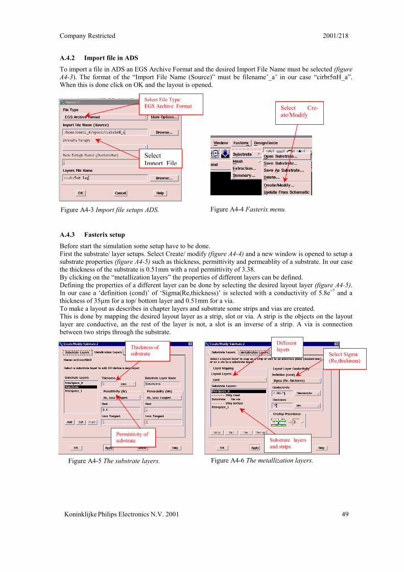
Company Restricted 2001/218
Koninklijke Philips Electronics N.V. 2001 49
Thickness ofsubstrate
Permittivity ofsubstrate
A.4.2 Import file in ADS
To import a file in ADS an EGS Archive Format and the desired Import File Name must be selected (figureA4-3). The format of the “Import File Name (Source)” must be filename’_a’ in our case “cirbr5nH_a”.When this is done click on OK and the layout is opened.
A.4.3 Fasterix setup
Before start the simulation some setup have to be done.First the substrate/ layer setups. Select Create/ modify (figure A4-4) and a new window is opened to setup asubstrate properties (figure A4-5) such as thickness, permittivity and permeablity of a substrate. In our casethe thickness of the substrate is 0.51mm with a real permittivity of 3.38.By clicking on the “metallization layers” the properties of different layers can be defined.Defining the properties of a different layer can be done by selecting the desired layout layer (figure A4-5).In our case a ‘definition (cond)’ of ‘Sigma(Re,thickness)’ is selected with a conductivity of 5.8e+7 and athickness of 35µm for a top/ bottom layer and 0.51mm for a via.To make a layout as describes in chapter layers and substrate some strips and vias are created.This is done by mapping the desired layout layer as a strip, slot or via. A strip is the objects on the layoutlayer are conductive, an the rest of the layer is not, a slot is an inverse of a strip. A via is connectionbetween two strips through the substrate.
Figure A4-3 Import file setups ADS. Figure A4-4 Fasterix menu.
Figure A4-5 The substrate layers. Figure A4-6 The metallization layers.
Select Cre-ate/Modify
Select Sigma(Re,thickness)
Differentlayers
Substrate layersand strips
SelectImport File
Select File Type:EGS Archive Format
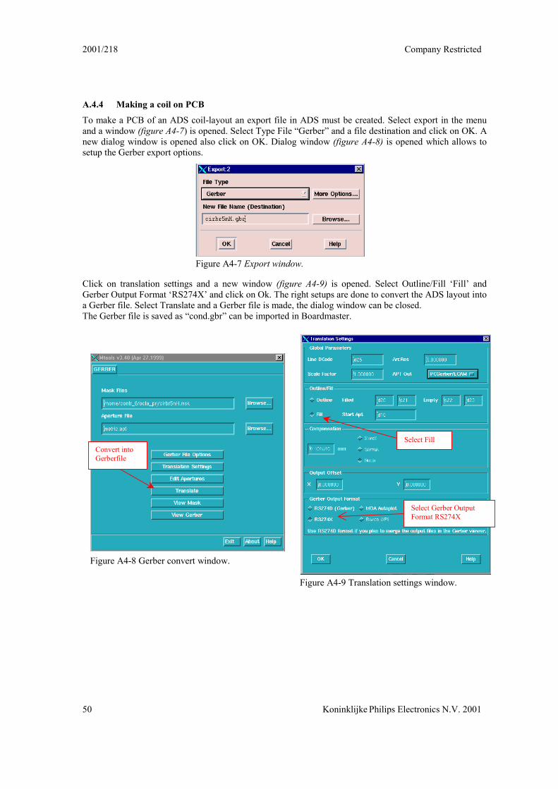
2001/218 Company Restricted
50 Koninklijke Philips Electronics N.V. 2001
Convert intoGerberfile
Select Gerber OutputFormat RS274X
Select Fill
A.4.4 Making a coil on PCB
To make a PCB of an ADS coil-layout an export file in ADS must be created. Select export in the menuand a window (figure A4-7) is opened. Select Type File “Gerber” and a file destination and click on OK. Anew dialog window is opened also click on OK. Dialog window (figure A4-8) is opened which allows tosetup the Gerber export options.
Click on translation settings and a new window (figure A4-9) is opened. Select Outline/Fill ‘Fill’ andGerber Output Format ‘RS274X’ and click on Ok. The right setups are done to convert the ADS layout intoa Gerber file. Select Translate and a Gerber file is made, the dialog window can be closed.The Gerber file is saved as “cond.gbr” can be imported in Boardmaster.
Figure A4-7 Export window.
Figure A4-8 Gerber convert window.
Figure A4-9 Translation settings window.
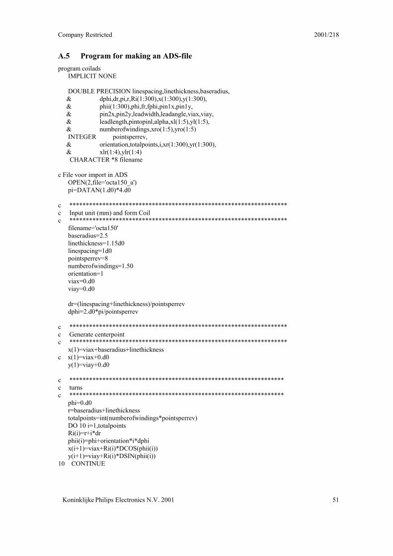
Company Restricted 2001/218
Koninklijke Philips Electronics N.V. 2001 51
A.5 Program for making an ADS-fileprogram coilads IMPLICIT NONE
DOUBLE PRECISION linespacing,linethickness,baseradius, & dphi,dr,pi,r,Ri(1:300),x(1:300),y(1:300), & phii(1:300),phi,fr,fphi,pin1x,pin1y, & pin2x,pin2y,leadwidth,leadangle,viax,viay, & leadlength,pintopinl,alpha,xl(1:5),yl(1:5), & numberofwindings,xro(1:5),yro(1:5) INTEGER pointsperrev, & orientation,totalpoints,i,xr(1:300),yr(1:300), & xlr(1:4),ylr(1:4) CHARACTER *8 filename
c File voor import in ADS OPEN(2,file='octa150_a') pi=DATAN(1.d0)*4.d0
c ******************************************************************c Input unit (mm) and form Coilc ****************************************************************** filename='octa150' baseradius=2.5 linethickness=1.15d0 linespacing=1d0 pointsperrev=8 numberofwindings=1.50 orientation=1 viax=0.d0 viay=0.d0
dr=(linespacing+linethickness)/pointsperrev dphi=2.d0*pi/pointsperrev
c ******************************************************************c Generate centerpointc ****************************************************************** x(1)=viax+baseradius+linethicknessc x(1)=viax+0.d0 y(1)=viay+0.d0
c *****************************************************************c turnsc ***************************************************************** phi=0.d0 r=baseradius+linethickness totalpoints=int(numberofwindings*pointsperrev) DO 10 i=1,totalpoints Ri(i)=r+i*dr phii(i)=phi+orientation*i*dphi x(i+1)=viax+Ri(i)*DCOS(phii(i)) y(i+1)=viay+Ri(i)*DSIN(phii(i))10 CONTINUE
2001/218 Company Restricted
52 Koninklijke Philips Electronics N.V. 2001
c *****************************************************************c Calculate endpoints of coil, fr=finalrc ***************************************************************** fr=r+numberofwindings*(linespacing+linethickness) fphi=orientation*(numberofwindings-int(numberofwindings))*2.d0*pi x(totalpoints+2)=viax+fr*dcos(fphi) y(totalpoints+2)=viay+fr*dsin(fphi) fr=fr-linethickness x(totalpoints+3)=viax+fr*dcos(fphi) y(totalpoints+3)=viay+fr*dsin(fphi) fr=fr+0.5d0*linethickness pin2x=viax+fr*dcos(fphi) pin2y=viay+fr*dsin(fphi)
c ******************************************************************c Calculate the point back towards the centerc ****************************************************************** r=baseradius DO 40 i=totalpoints,0,-1 Ri(i+1)=r+i*dr phii(i+1)=phi+orientation*i*dphi x(2*totalpoints+4-i)=viax+Ri(i+1)*DCOS(phii(i+1)) y(2*totalpoints+4-i)=viay+Ri(i+1)*DSIN(phii(i+1))40 CONTINUE
c ******************************************************************c close loopc ****************************************************************** x(2*totalpoints+5)=x(1) y(2*totalpoints+5)=y(1)
c *****************************************************************c Generate the leadwirec ***************************************************************** leadwidth=linethicknessc alpha=DATAN(baseradius/fr)c leadangle=fphi+orientation*alpha leadangle=pi/4.d0 pintopinl=DSQRT(baseradius+fr*fr) leadlength=pintopinl+leadwidth xl(1)=-0.5d0*leadwidth yl(1)=-0.5d0*leadwidth xl(2)=-0.5d0*leadwidth yl(2)=0.5d0*leadwidth xl(3)=-0.5d0*leadwidth+leadlength yl(3)=0.5d0*leadwidth xl(4)=-0.5d0*leadwidth+leadlength yl(4)=-0.5d0*leadwidth xl(5)=pintopinl yl(5)=0.d0
Company Restricted 2001/218
Koninklijke Philips Electronics N.V. 2001 53
c ******************************************************************c Rotatec ****************************************************************** xro(1)=dcos(leadangle)*xl(1)-dsin(leadangle)*yl(1) & +baseradius+0.5d0*linethickness yro(1)=dsin(leadangle)*xl(1)+dcos(leadangle)*yl(1) xro(2)=dcos(leadangle)*xl(2)-dsin(leadangle)*yl(2)+baseradius & +0.5d0*linethickness yro(2)=dsin(leadangle)*xl(2)+dcos(leadangle)*yl(2) xro(3)=dcos(leadangle)*xl(3)-dsin(leadangle)*yl(3) & +baseradius+0.5d0*linethickness yro(3)=dsin(leadangle)*xl(3)+dcos(leadangle)*yl(3) xro(4)=dcos(leadangle)*xl(4)-dsin(leadangle)*yl(4)+baseradius & +0.5d0*linethickness yro(4)=dsin(leadangle)*xl(4)+dcos(leadangle)*yl(4) xro(5)=dcos(leadangle)*xl(5)-dsin(leadangle)*yl(5)+baseradius & +0.5d0*linethickness yro(5)=dsin(leadangle)*xl(5)+dcos(leadangle)*yl(5)
write(2,*) '$$ filename',' = ',filename write(2,*) '$$ baseradius',' = ',baseradius write(2,*) '$$ linethickness',' = ',linethickness write(2,*) '$$ linespacing',' = ',linespacing write(2,*) '$$ pointsperrev',' = ',pointsperrev write(2,*) '$$ numberofwindings',' = ',numberofwindings write(2,*) write(2,*) write(2,*) 'UNITS UM,10000;' write(2,*) 'GRID 0.1000,2 0.0000,0.0000;' write(2,*) 'LOCK 0.0000;' write(2,*) 'TSLANT 0.0000;' write(2,*) 'RESOLUTION 0.0000;' write(2,*) '$$' write(2,*) '$$ layer line' write(2,*) '$$ label type type color pen layer' write(2,*) '$$' write(2,*) write(2,*) 'EQU ','cond',' :D',' :L1',' :C15',' :P1',' 1;' write(2,*) 'EXIT;' write(2,*)c aanpassen van filenaam write(2,*) '$FILES ',filename,'$;' write(2,*) write(2,*) 'EDIT;' write(2,*) 'EDIT;' write(2,*) write(2,*) 'EDIT ',filename,';' write(2,*) 'GRID 0.0001,1 0.0000,0.0000;' write(2,*) 'ADD P1 :W0.0000'
DO 30 i=1,2*totalpoints+5 IF ((x(i)).GE.0.d0) THEN xr(i)=INT(1000.d0*x(i)+0.5d0) ELSE xr(i)=INT(1000.d0*x(i)-0.5d0) ENDIF IF ((y(i)).GE.0.d0) THEN
2001/218 Company Restricted
54 Koninklijke Philips Electronics N.V. 2001
yr(i)=INT(1000.d0*y(i)+0.5d0) ELSE yr(i)=INT(1000.d0*y(i)-0.5d0) ENDIF write(2,*) xr(i),', ',yr(i)
30 CONTINUE write(2,*)c write(2,*) 'ARE ',' ''NET_0'' ',' ''signal_2'' ',' SOLID ',c & '4'
DO 50 i=1,4 IF ((xro(i)).GE.0.d0) THEN xlr(i)=INT(1000.d0*xro(i)+0.5d0) ELSE xlr(i)=INT(1000.d0*xro(i)-0.5d0) ENDIF IF ((yro(i)).GE.0.d0) THEN ylr(i)=INT(1000.d0*yro(i)+0.5d0) ELSE ylr(i)=INT(1000.d0*yro(i)-0.5d0) ENDIFc write(2,*) ' ',xlr(i),',',c & ylr(i)50 CONTINUE write(2,*) ';' write(2,*) 'Grid 0.1000,1 0.0000,0.0000;' write(2,*) 'SAVE;' write(6,*) 'Pin 1: ',xro(5),',',yro(5) write(6,*) 'Pin 2: ', pin2x,',',pin2y write(6,*) 'viax ',viax+baseradius+0.5d0*linethickness write(6,*) 'viay ',viay CLOSE(2) END
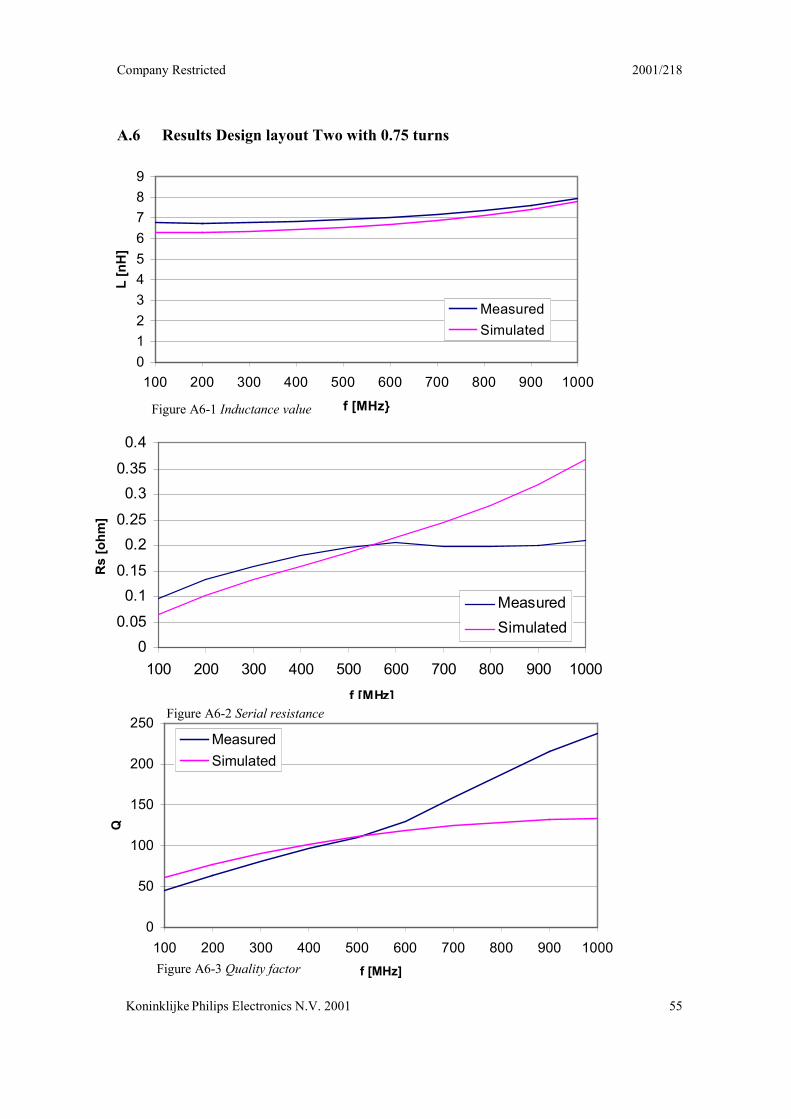
Company Restricted 2001/218
Koninklijke Philips Electronics N.V. 2001 55
00.050.1
0.150.2
0.250.3
0.350.4
100 200 300 400 500 600 700 800 900 1000f [MHz]
Rs
[ohm
]
MeasuredSimulated
0
50
100
150
200
250
100 200 300 400 500 600 700 800 900 1000f [MHz]
Q
MeasuredSimulated
0123456789
100 200 300 400 500 600 700 800 900 1000f [MHz}
L [n
H]
MeasuredSimulated
A.6 Results Design layout Two with 0.75 turns
Figure A6-1 Inductance value
Figure A6-3 Quality factor
Figure A6-2 Serial resistance
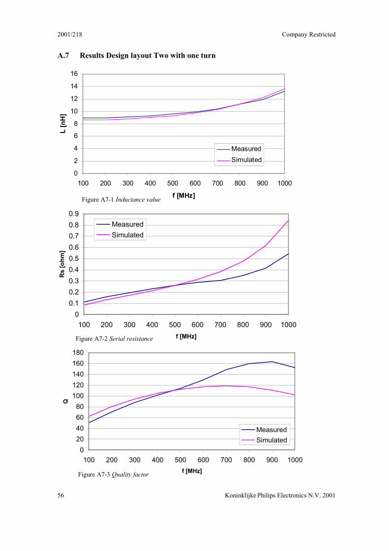
2001/218 Company Restricted
56 Koninklijke Philips Electronics N.V. 2001
00.10.20.30.40.50.60.70.80.9
100 200 300 400 500 600 700 800 900 1000f [MHz]
Rs
[ohm
]
MeasuredSimulated
020406080
100120140160180
100 200 300 400 500 600 700 800 900 1000f [MHz]
Q
MeasuredSimulated
0
2
4
6
8
10
12
14
16
100 200 300 400 500 600 700 800 900 1000
f [MHz]
L [n
H]
MeasuredSimulated
A.7 Results Design layout Two with one turn
Figure A7-1 Inductance value
Figure A7-2 Serial resistance
Figure A7-3 Quality factor
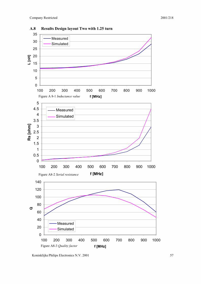
Company Restricted 2001/218
Koninklijke Philips Electronics N.V. 2001 57
00.5
11.5
22.5
33.5
44.5
5
100 200 300 400 500 600 700 800 900 1000
f [MHz]
Rs
[ohm
]
MeasuredSimulated
0
5
10
15
20
25
30
35
100 200 300 400 500 600 700 800 900 1000f [MHz]
L [n
H]
MeasuredSimulated
0
20
40
60
80
100
120
140
100 200 300 400 500 600 700 800 900 1000f [MHz]
Q
MeasuredSimulated
A.8 Results Design layout Two with 1.25 turn
Figure A 8-1 Inductance value
Figure A8-2 Serial resistance
Figure A8-3 Quality factor
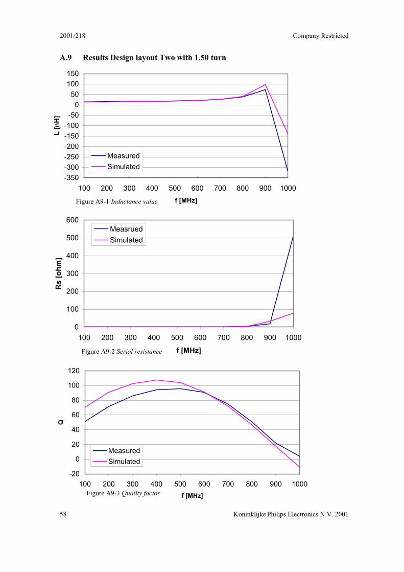
2001/218 Company Restricted
58 Koninklijke Philips Electronics N.V. 2001
0
100
200
300
400
500
600
100 200 300 400 500 600 700 800 900 1000
f [MHz]
Rs
[ohm
]
MeasruedSimulated
-20
0
20
40
60
80
100
120
100 200 300 400 500 600 700 800 900 1000f [MHz]
Q
MeasuredSimulated
-350-300-250-200-150-100-50
050
100150
100 200 300 400 500 600 700 800 900 1000f [MHz]
L [n
H]
MeasuredSimulated
A.9 Results Design layout Two with 1.50 turn
Figure A9-1 Inductance value
Figure A9-3 Quality factor
Figure A9-2 Serial resistance
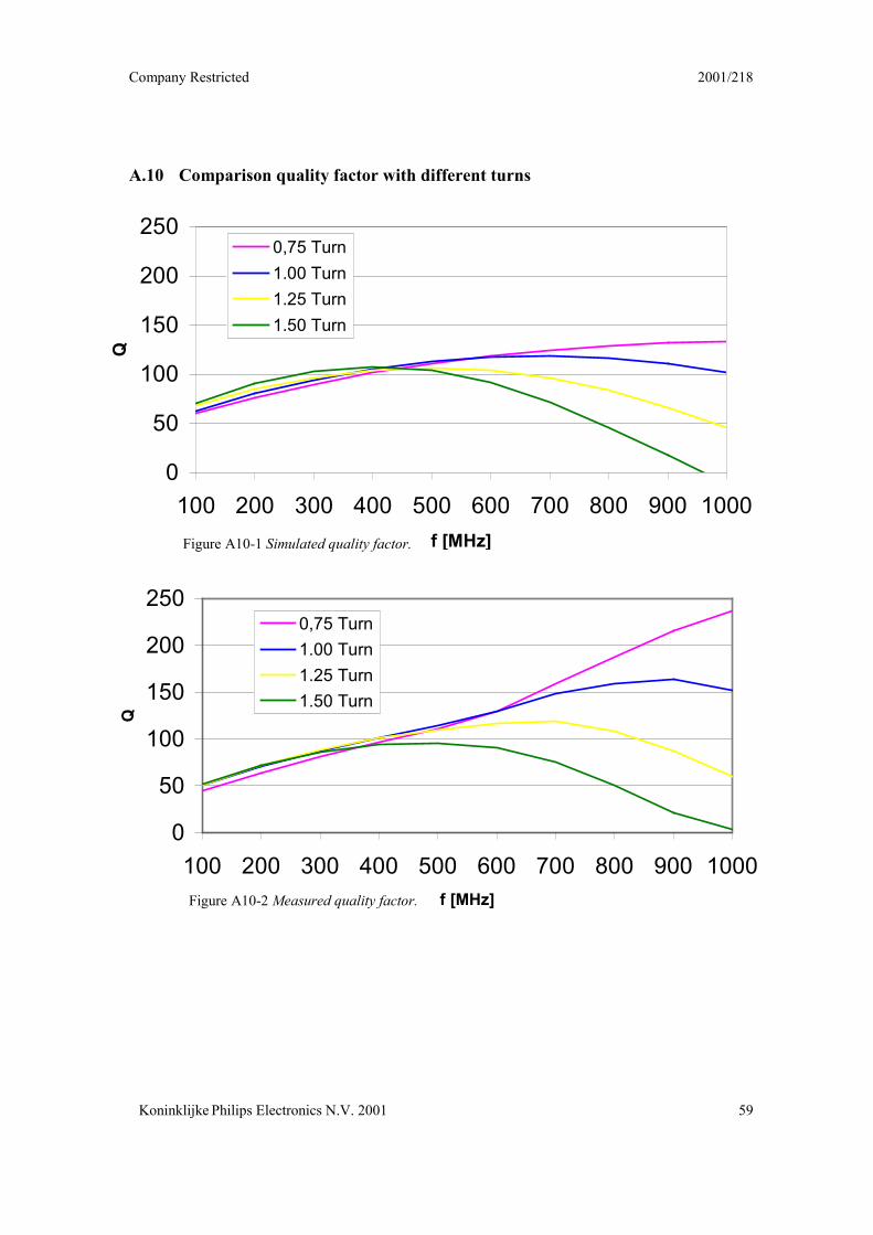
Company Restricted 2001/218
Koninklijke Philips Electronics N.V. 2001 59
0
50
100
150
200
250
100 200 300 400 500 600 700 800 900 1000f [MHz]
Q
0,75 Turn1.00 Turn1.25 Turn1.50 Turn
0
50
100
150
200
250
100 200 300 400 500 600 700 800 900 1000f [MHz]
Q
0,75 Turn1.00 Turn1.25 Turn1.50 Turn
A.10 Comparison quality factor with different turns
Figure A10-1 Simulated quality factor.
Figure A10-2 Measured quality factor.
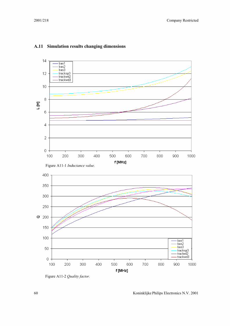
2001/218 Company Restricted
60 Koninklijke Philips Electronics N.V. 2001
A.11 Simulation results changing dimensions
Figure A11-1 Inductance value.
Figure A11-2 Quality factor.
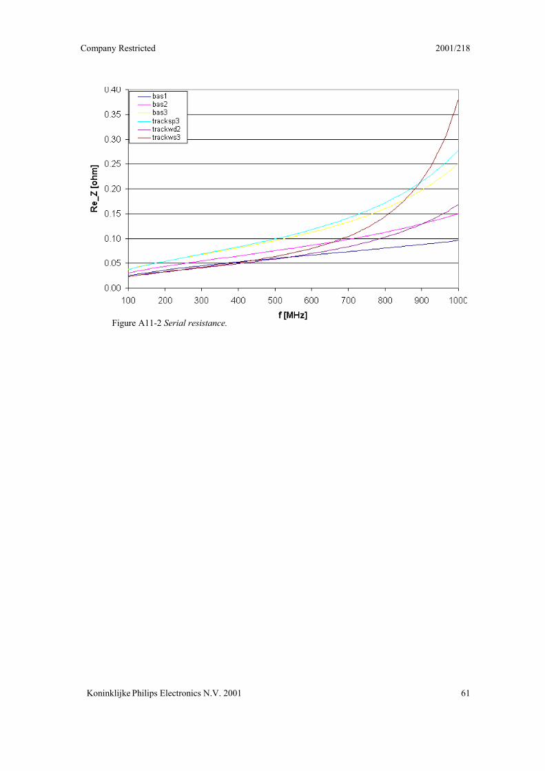
Company Restricted 2001/218
Koninklijke Philips Electronics N.V. 2001 61
Figure A11-2 Serial resistance.
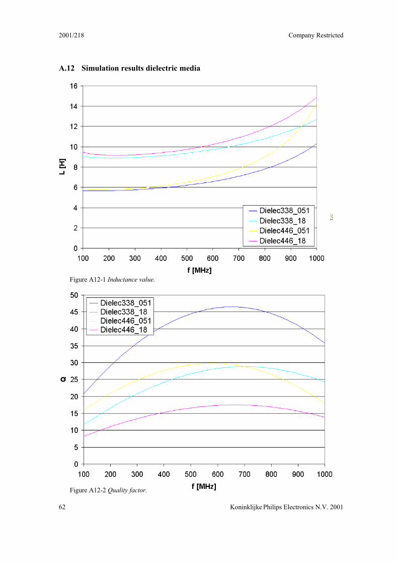
2001/218 Company Restricted
62 Koninklijke Philips Electronics N.V. 2001
A.12 Simulation results dielectric media
Figure A12-2 Quality factor.
Figure A12-1 Inductance value.
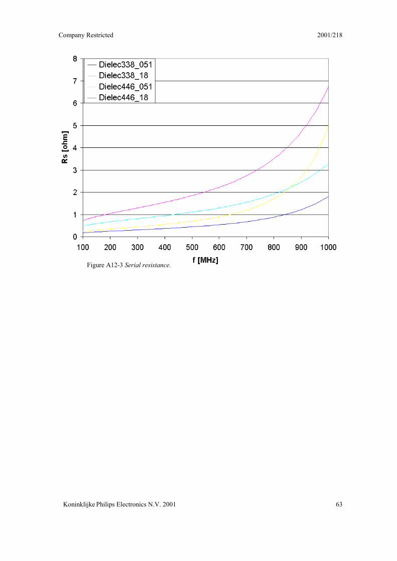
Company Restricted 2001/218
Koninklijke Philips Electronics N.V. 2001 63
Figure A12-3 Serial resistance.
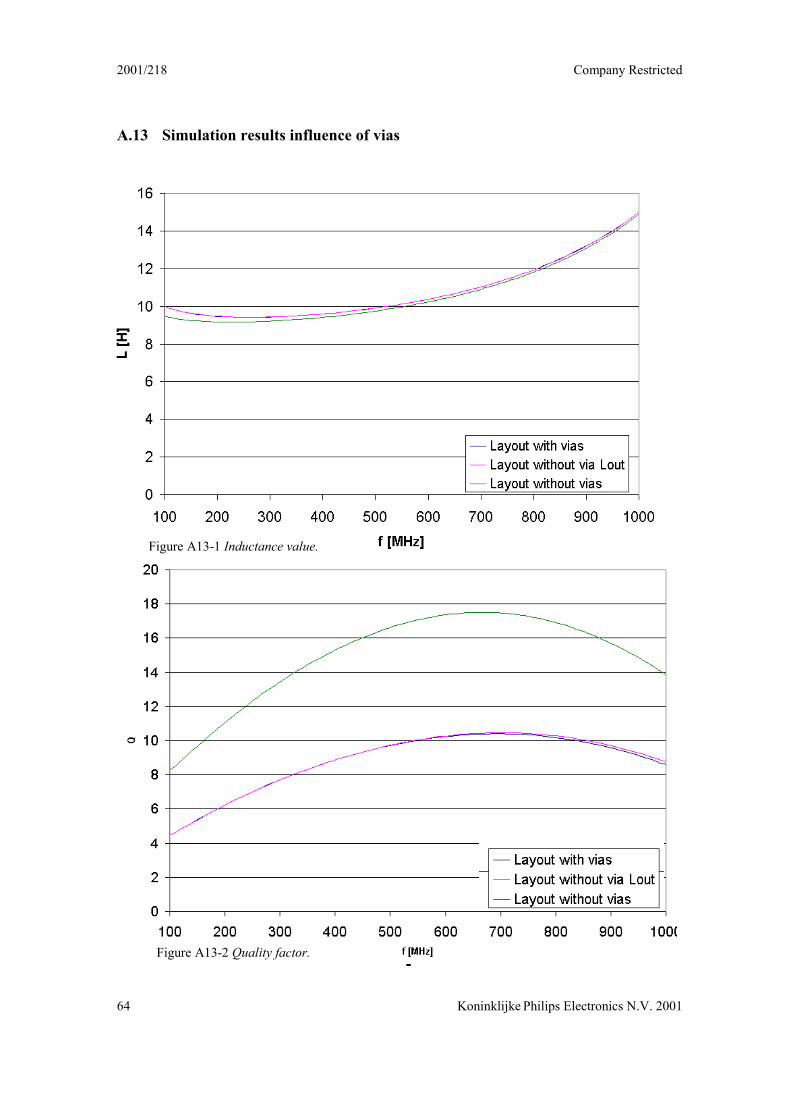
2001/218 Company Restricted
64 Koninklijke Philips Electronics N.V. 2001
A.13 Simulation results influence of vias
Figure A13-1 Inductance value.
Figure A13-2 Quality factor.
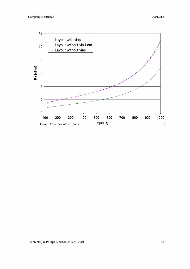
Company Restricted 2001/218
Koninklijke Philips Electronics N.V. 2001 65
Figure A13-3 Serial resistance.

Company Restricted 2001/218
Koninklijke Philips Electronics N.V. 2001 67
Author(s): Michel de Clercq and Tarik Saric
Title: Coils on PCB
Distribution
Nat.Lab./PI WB-5PRL Redhill, UKPRB Briarcliff Manor, USALEP Limeil-Brévannes, FrancePFL Aachen, GermanyCP&T WAH
Director: Ir. G.G.M. Beenker WAY-52Department Head Ir. A. Jongepier WAY-31Department Head Dr. ir. P.W. Hooijmans WAY-52
Abstract
Paul Bachrach Nat.Lab. WAY-31Henk v.d. Donk Nat.Lab. WAY-31Els van Duren Nat.Lab. WAY-31Dick Eekel Nat.Lab. WAY-31Barbara Collette Nat.Lab. WAY-31Jos Dohmen Nat.Lab. WAY-31Marian Driessen Nat.Lab. WAY-31Maria Floren Nat.Lab. WAY-31Jaap Fijnvandraat Nat.Lab. WAY-31Marcel Hanssen Nat.Lab. WAY-31Roland Hermans Nat.Lab. WAY-31Remco de Jager Nat.Lab. WAY-31Marinus Kluitmans Nat.Lab. WAY-31Linda Lengowski Nat.Lab. WAY-31John van Neerven Nat.Lab. WAY-31Jos Peters Nat.Lab. WAY-31Marcel Sevat Nat.Lab. WAY-31Jan Symons Nat.Lab. WAY-31Ron Vennix Nat.Lab. WAY-31Geert Warrink Nat.Lab. WAY-31

2001/218 Company Restricted
68 Koninklijke Philips Electronics N.V. 2001
Full reportJan van Gerwen Nat.Lab. WAY-31Rick Janssen Nat.Lab. WAY-31Marq Kole Nat.Lab. WAY-31Achie Lin Nat.Lab. WAY-31Jan ter Maten Nat.Lab. WAY-31Jan Niehof Nat.Lab. WAY-31Eduardo Alarcon Rivero Nat.Lab. WAY-31Tony Strachan Nat.Lab. WAY-31R.P. Aditham Nat.Lab. WAY-51M.Apostolidou Nat.Lab. WAY-51H. Brekelmans Nat.Lab. WAY-51M. Collados Nat.Lab WAY-51J. Dekkers Nat.Lab. WAY-51D. Delas Nat.Lab. WAY-51G. Dolmans Nat.Lab. WAY-51E. Dugast Nat.Lab. WAY-51D. van Goor Nat.Lab. WAY-51G. Grillo Nat.Lab. WAY-51F. Hurkx Nat.Lab. WAY-51E. van der Heijden Nat.Lab. WAY-51D. Jeurissen Nat.Lab. WAY-51G. de Jong Nat.Lab. WAY-51D. Leenaerts Nat.Lab. WAY-51L. Leyten Nat.Lab. WAY-51P. Mattheijssen Nat.Lab. WAY-51M. Notten Nat.Lab. WAY-51N. Pavlovic Nat.Lab. WAY-51M. Sanduleanu Nat.Lab. WAY-51J. van Sinderen Nat.Lab. WAY-51E. Stikvoort Nat.Lab. WAY-51A. Tombeur Nat.Lab. WAY-51B. Vandewiele Nat.Lab. WAY-51C. Vaucher Nat.Lab. WAY-51H. Veenstra Nat.Lab. WAY-51P. van de Ven Nat.Lab. WAY-51P. de Vreede Nat.Lab. WAY-51J. Vromans Nat.Lab. WAY-51G. Wetzker Nat.Lab. WAY-51H. v/d Wijst KrefeldM. Barnasconi RF-Modules

Company Restricted 2001/218
Koninklijke Philips Electronics N.V. 2001 69