Embed Size (px)
Citation preview

1
CMOS VLSI IC Design
A decent understanding of all tasks required to design and fabricate a chip takes years of experience

2
Commonly used keywords
• INTEGRATED CIRCUIT (IC)many transistors on one chip
VERY LARGE SCALE INTEGRATION (VLSI)very many transistors (> 10000 gates) on one chip
COMPLEMENTARY METAL OXIDE SEMICONDUCTOR (CMOS) TECHNOLOGYcheap, high integration density, low power

3
Integrated Circuits

4
The Silicon Wafer

5
Packaging the Chip

6
Common Packages

7
Impact of ICs industry
Integrated Circuits enabled today’s way of life1018 transistors manufactured in 2003
(100 million for every human on the planet)

8
Moore's Law In 1963 Gordon Moore predicted that as a result
of continuous miniaturization transistor count would double every 18 months
53% compound annual growth rate over 45 years (No other technology has grown so fast so long)
Transistors have become: - smaller - faster - consume less power - cheaper to manufacture

9
Challenges
• The greatest challenge in modern VLSI design is managing system complexity
• Strategies used to cope with Complexity
– Abstraction – Structured Design Approach– Design Flow

10
Design Abstractions
1970 1980 1990 2000+
Ab
stra
ctio
n
Transistor Level
Gate Level
RTL
Register Transfer Level
(HDL)
RTL SW
System Level

11
Examples of design abstractions (1)A
B
Z
S
0
1
Z = A S' + B S
Logic Level
Truth Table
MSI Building Block
Gate Level
Switch Level
Module Level

12
Examples of design abstractions (2)
Structural Level VHDL
Register Transfer Level VHDLMOS transistors Level

13
Structured Design• Hierarchy
– Divide and Conquer paradigm
• Modularity
– Well-defined interfaces allow modules to be treated as black boxes
• Regularity
– It makes easier to reuse blocks
• Standard cell libraries are a very good example of modularity and regularity

14
IC Design Hierarchy

15
Standard cells

16
Simplified IC Design Flows

17
Another Simplified IC Design Flow
Implementation:• Translation (merge all design files into a single netlist)• Device mapping• P&R
Device Programming:• Generation conf. file • Download conf. file into device

18
RTL code (Verilog)
assign cout = (a&b) | (a&c) | (b&c);

19
Gate level netlist (Verilog)
module carry(input a, b, c, output cout)
wire x, y, z;
and g1(x, a, b);and g2(y, a, c);and g3(z, b, c);or g4(cout, x, y, z);
endmodule
ab
ac
bc
cout
x
y
z
g1
g2
g3
g4

20
Transistor level netlist (Verilog)
a b
c
c
a b
b
a
a
b
coutcn
n1 n2
n3
n4
n5 n6
p6p5
p4
p3
p2p1
i1
i3
i2
i4
module carry(input a, b, c, output cout)
wire i1, i2, i3, i4, cn;
tranif1 n1(i1, 0, a);tranif1 n2(i1, 0, b);tranif1 n3(cn, i1, c);tranif1 n4(i2, 0, b);tranif1 n5(cn, i2, a);tranif0 p1(i3, 1, a);tranif0 p2(i3, 1, b);tranif0 p3(cn, i3, c);tranif0 p4(i4, 1, b);tranif0 p5(cn, i4, a);tranif1 n6(cout, 0, cn);tranif0 p6(cout, 1, cn);
endmodule

21
SPICE netlist.SUBCKT CARRY A B C COUT VDD GNDMN1 I1 A GND GND NMOS W=1U L=0.18U AD=0.3P AS=0.5PMN2 I1 B GND GND NMOS W=1U L=0.18U AD=0.3P AS=0.5PMN3 CN C I1 GND NMOS W=1U L=0.18U AD=0.5P AS=0.5PMN4 I2 B GND GND NMOS W=1U L=0.18U AD=0.15P AS=0.5PMN5 CN A I2 GND NMOS W=1U L=0.18U AD=0.5P AS=0.15PMP1 I3 A VDD VDD PMOS W=2U L=0.18U AD=0.6P AS=1 PMP2 I3 B VDD VDD PMOS W=2U L=0.18U AD=0.6P AS=1PMP3 CN C I3 VDD PMOS W=2U L=0.18U AD=1P AS=1PMP4 I4 B VDD VDD PMOS W=2U L=0.18U AD=0.3P AS=1PMP5 CN A I4 VDD PMOS W=2U L=0.18U AD=1P AS=0.3PMN6 COUT CN GND GND NMOS W=2U L=0.18U AD=1P AS=1PMP6 COUT CN VDD VDD PMOS W=4U L=0.18U AD=2P AS=2PCI1 I1 GND 2FFCI3 I3 GND 3FFCA A GND 4FFCB B GND 4FFCC C GND 2FFCCN CN GND 4FFCCOUT COUT GND 2FF.ENDS

22
Types of ICs• ASSP• ASIC
Full-custom Semi-custom
Cell Based Gate Arrays
Programmable CPLD and
FPGA
Use
Design Style

23
Standard Cells
Rows of standardcells with routing channels between them
Memory array

24
Gate Arrays

25
Field Programmable Gate Array
(CLB)

26
Internal Structure of a CLB

27
Various on chip structures
• Random logic
• Data paths
• Arrays
• Analog
• Input/output (I/O)

28
Example of random Logic
• Synthesized MIPS controller

29
Another example of random logic
• Synthesized MIPS

30
Example of data path
• Hand-Crafted MIPS datapath
31
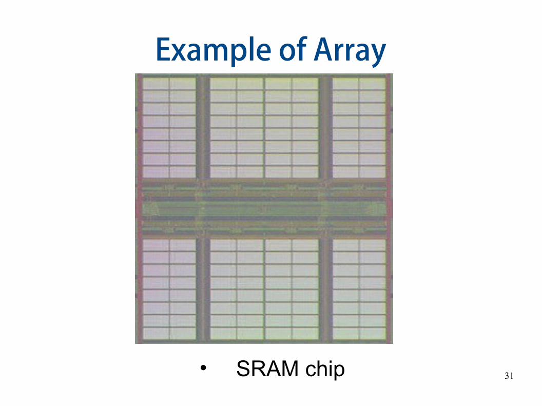
Example of Array
• SRAM chip

32
Example of Analog structure
• Charge Pump Phase-Locked Loop

33
Example of I/O

34
Bidirectional I/O PAD circuit
5

35
Physical Design
• Floorplanning and area estimation
• Standard Cell Based Layout – Place and Route
– Parasitic Extraction
– Post Layout Verification
• Data-path Based Layout– Slice Planning
– Parasitic Extraction
– Post Layout Verification

36
Floorplanning
• Does the design fit the chip area budgeted ?
• Estimates area of major units and defines their relative placement
• Estimate wire lengths
• Estimate wiring congestion

37
Area Estimation
• Some cell library vendor specify cell layout densities in Kgates/mm2
• Compare to another block you already designed or estimate from transistor counts
• Budget room for large wiring tracks

38
Example of Layout

39
CAD Tools Designers rely increasingly on design automation software tools to
seek productivity gains and to cope with increased complexity
• Design Entry• Schematic capture• Hardware Description Languages
• Logic Synthesis• Pre layout verification
• Functional simulation• Formal methods• Timing Analysis
• Floorplanning• Placement• Routing• Extraction• Post layout verification
Logic
Design
Physical
Design
Typical Design Flow

40
Verification• Fabrication is slow & expensive
• MOSIS 0.6 µm masks: $1000, 3 months
• State of art masks (130nm): $1M, 1 month
• Debugging chips is very hard
• Limited visibility into operation
• Prove design is right before building!
• System simulation & performance Assessment (C/C++)
• Logic Simulation / formal verification / STA
• Circuit simulation
• Layout vs. schematic comparison (LVS)
• Design & electrical rule checks (DRC, ERC)
• Verification is > 50% of effort on most chips !

41
Fabrication
• Tapeout final layout
– Formats for mask descriptions: CIF (academia) and GDS II (industry)
• Fabrication
– 6, 8, 12” wafers (bare wafer costs $1000-$5000)
– Optimized for throughput, not latency (turnaround times up to 10 weeks !)
– Cut into individual dice
• Fabs cost billions of dollars and become obsolete in a few years
– Fabless semiconductor companies
– Manufacturing Companies: TSMS, UMC, IBM

42
Testing
• Test that chip operates as expected– Design errors
– Manufacturing errors
• A single dust particle or wafer defect kills a die– Yields from 90% to < 10%
– Depends on die size, maturity of process
– Test each part before shipping to customer

43
Summary
• Chip Design requires a fundamental understanding of circuit and physical design
• This is true even if many chip designers spend much of their time specifying circuits with HDL and seldom look at the actual transistors
• The best way to learn VLSI design is by doing it !

44
MOS Transistors (POS to be picky)
TRANS-ISTOR (=TRANSFER-RESISTOR) Four terminals: gate, source, drain, body (= bulk)

45
Our first CMOS circuit