Embed Size (px)
Citation preview

CMOS VLSI For Computer Engineering
Lecture 4 – Logical Effort
Prof. Luke Theogarajan
parts adapted form Harris – www.cmosvlsi.com and Rabaey-
http://bwrc.eecs.berkeley.edu/icbook/slides.htm
CMOS VLSI for Computer Engineering
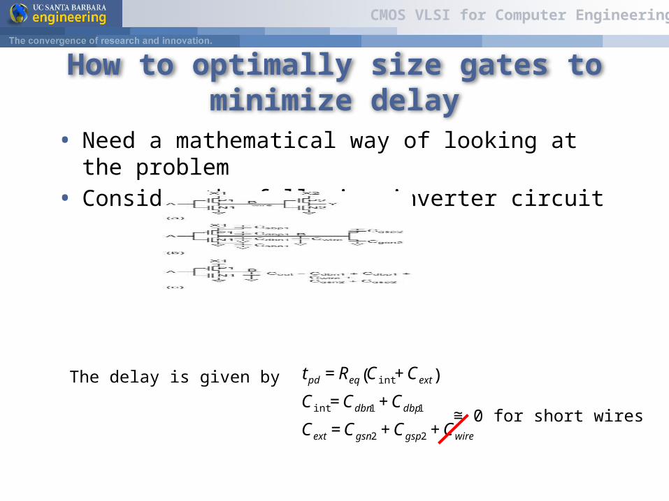
How to optimally size gates to minimize delay
• Need a mathematical way of looking at the problem
• Consider the following inverter circuit
The delay is given by
€
tpd = Req Cint +Cext( )
Cint =Cdbn1 +Cdbp1
Cext =Cgsn2 +Cgsp2 +Cwire
≅ 0 for short wires
CMOS VLSI for Computer Engineering
€
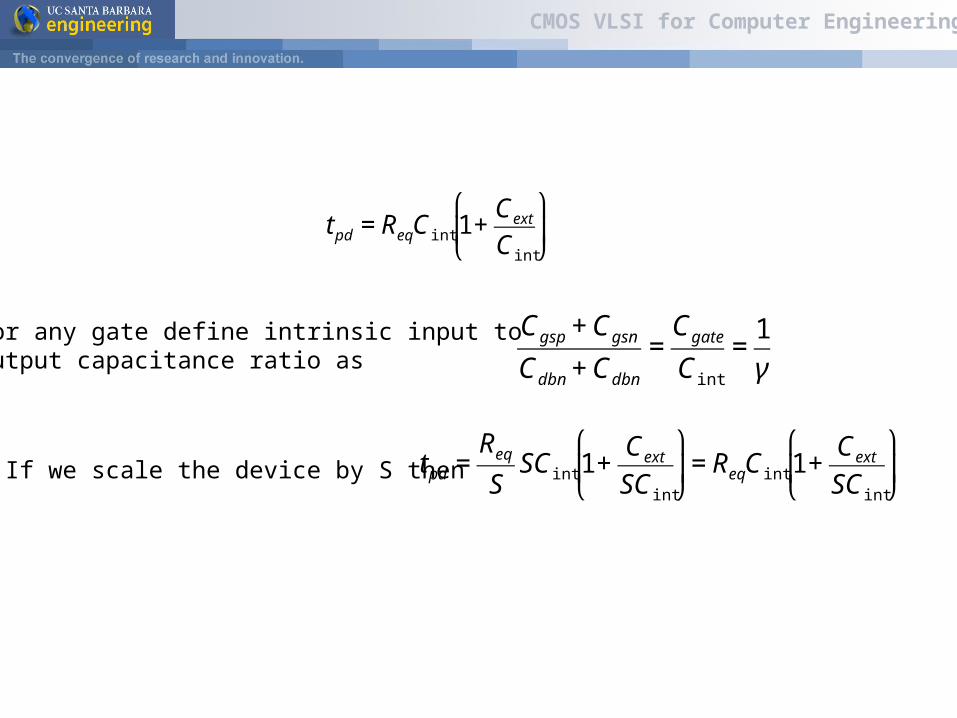
tpd = ReqCint 1+Cext
Cint
⎛
⎝ ⎜
⎞
⎠ ⎟
€
Cgsp +Cgsn
Cdbn +Cdbn
=Cgate
Cint
=1
γFor any gate define intrinsic input to output capacitance ratio as
If we scale the device by S then
€
tpd =Req
SSCint 1+
Cext
SCint
⎛
⎝ ⎜
⎞
⎠ ⎟= ReqCint 1+
Cext
SCint
⎛
⎝ ⎜
⎞
⎠ ⎟

CMOS VLSI for Computer Engineering
Delay as a function of S
S
Delay
So there must be an optimum
Delay of driver goes up!

CMOS VLSI for Computer Engineering
Path delay
Need to look at overall path if delay optimization is desired, consider N inverters,The delay of any inverter i is given by:
€
tpdi = ReqCeq 1+Cgate,i+1
Cint,i
⎛
⎝ ⎜
⎞
⎠ ⎟= ReqCeq 1+
Cgate,i+1
γCgate,i
⎛
⎝ ⎜ ⎜
⎞
⎠ ⎟ ⎟
N1
CL
Also CN+1 = CL
CMOS VLSI for Computer Engineering
Optimal delay
€
∂t pd∂Ci
= 0For optimal delay set
Collect terms due to Ci and differentiate
€
tpd = t p0 1+Ci+1
γCi
⎛
⎝ ⎜
⎞
⎠ ⎟
1
N
∑
tp0 = ReqCint
Total path delay with CN+1 = CL
€
∂∂Ci
Ci
γCi−1
+Ci+1
γCi
⎛
⎝ ⎜
⎞
⎠ ⎟= 0
€
1
γCi−1
−Ci+1
γCi2
= 0

CMOS VLSI for Computer Engineering
Optimal Delay
€
Ci = Ci+1Ci−1
Optimal delay occurs when the size is the geometric mean of the neighbors!
The above equation can be satisfied when each gate is sized h times its driversince
€
Ci+1
Ci
=Ci
Ci−1
= h
h is called the fanout of the gate

CMOS VLSI for Computer Engineering
Optimal Delay for a chain of inverters
€
tpd = t p0 1+h
γ
⎛
⎝ ⎜
⎞
⎠ ⎟
1
N
∑ = Nt p0 1+h
γ
⎛
⎝ ⎜
⎞
⎠ ⎟
If we want to size purely based on final load then define
€
H =CL
Cgate1
€
h = HN
tpd = Nt p0 1+HN
γ
⎛
⎝ ⎜
⎞
⎠ ⎟

CMOS VLSI for Computer Engineering
6: Logical Effort 9
How to design any path?
• Chip designers face a bewildering array of choices What is the best circuit topology for a function? How many stages of logic give least delay? How wide should the transistors be?
• Logical effort is a method to make these decisions Uses a simple model of delay Allows back-of-the-envelope calculations Helps make rapid comparisons between alternatives Emphasizes remarkable symmetries
? ? ?

CMOS VLSI for Computer Engineering
6: Logical Effort 10
Example
• Ben Bitdiddle is the memory designer for the Motoroil 68W86, an embedded automotive processor. Help Ben design the decoder for a register file.
• Decoder specifications: 16 word register file Each word is 32 bits wide Each bit presents load of 3 unit-sized transistors True and complementary address inputs A[3:0] Each input may drive 10 unit-sized transistors
• Ben needs to decide: How many stages to use? How large should each gate be? How fast can decoder operate?
A[3:0] A[3:0]
16
32 bits
16 words
4:16 D
ecoder
Register File

CMOS VLSI for Computer Engineering
6: Logical Effort 11
Delay in a Logic Gate
• Express delays in process-independent unit• Delay has two components: d = f + p• f: effort delay = gh (a.k.a. stage effort)
Again has two components• g: logical effort
Measures relative ability of gate to deliver current g 1 for inverter
• h: electrical effort = Cout / Cin
Ratio of output to input capacitance Sometimes called fanout
• p: parasitic delay Represents delay of gate driving no load Set by internal parasitic capacitance
absdd
=t 3RC
3 ps in 65 nm process
60 ps in 0.6 mm process
CMOS VLSI for Computer Engineering
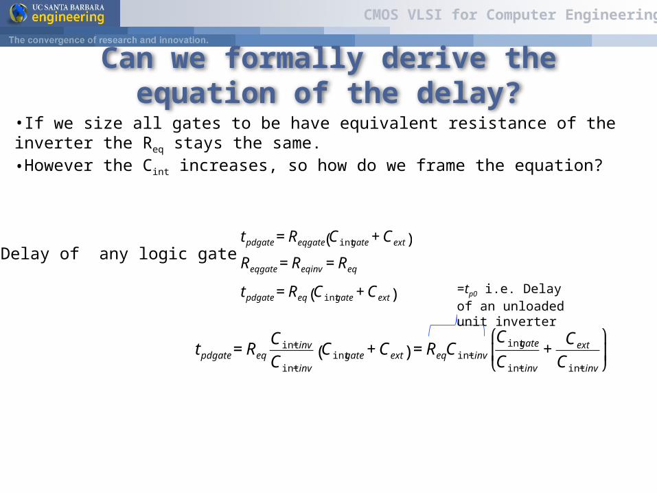
Can we formally derive the equation of the delay?
•If we size all gates to be have equivalent resistance of the inverter the Req stays the same.•However the Cint increases, so how do we frame the equation?
Delay of any logic gate
€
tpdgate = Reqgate Cint gate +Cext( )
Reqgate = Reqinv = Req
tpdgate = Req Cint gate +Cext( )
€
tpdgate = Req
Cint−inv
Cint−inv
Cint gate +Cext( ) = ReqCint−inv
Cint gate
Cint−inv
+Cext
Cint−inv
⎛
⎝ ⎜
⎞
⎠ ⎟
=tp0 i.e. Delay of an unloaded unit inverter
CMOS VLSI for Computer Engineering
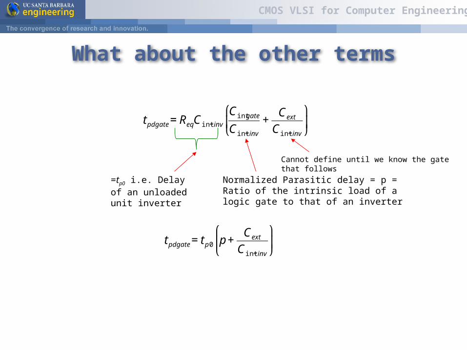
What about the other terms
€
tpdgate = ReqCint−inv
Cint gate
Cint−inv
+Cext
Cint−inv
⎛
⎝ ⎜
⎞
⎠ ⎟
=tp0 i.e. Delay of an unloaded unit inverter
Normalized Parasitic delay = p = Ratio of the intrinsic load of a logic gate to that of an inverter
Cannot define until we know the gate that follows
€
tpdgate = t p0 p+Cext
Cint−inv
⎛
⎝ ⎜
⎞
⎠ ⎟

CMOS VLSI for Computer Engineering
Optimizing the delay of a logic path
Consider a generic logic path
What is the total delay of the path?

CMOS VLSI for Computer Engineering
€
tdelay = tp0 pi +C i+1
gate
Cint−inv
⎛
⎝ ⎜
⎞
⎠ ⎟
i=1
N
∑
If we assume all gates are sized to have the same effective resistance as the inverter for which tp0 is calculated then we have:
Need a more tractable form, see if we can manipulate the equation to give us the fanout
€
tdelay = tp0 pi +C i+1
gate
Cint−inv
C igate
C igate
⎛
⎝ ⎜
⎞
⎠ ⎟
i=1
N
∑ = t p0 pi +C i+1
gate
C igate
C igate
Cint−inv
⎛
⎝ ⎜
⎞
⎠ ⎟
i=1
N
∑
CMOS VLSI for Computer Engineering
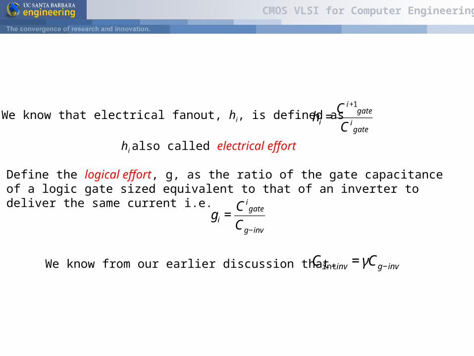
We know that electrical fanout, hi, is defined as
€
hi =C i+1
gate
C igate
Define the logical effort, g, as the ratio of the gate capacitance of a logic gate sized equivalent to that of an inverter to deliver the same current i.e.
€
gi =C i
gate
Cg−inv
We know from our earlier discussion that
€
Cint−inv = γCg−inv
hi also called electrical effort

CMOS VLSI for Computer Engineering
Almost there
€
tdelay = tp0 pi +gihi
γ
⎛
⎝ ⎜
⎞
⎠ ⎟
i=1
N
∑Combining, we get
Define fi = gihi, where f is know as the stage effort
€
tdelay = tp0 pi +f iγ
⎛
⎝ ⎜
⎞
⎠ ⎟
i=1
N
∑
€
tdelay = tp0 pi
i=1
N
∑ +f iγi=1
N
∑ ⎛
⎝ ⎜
⎞
⎠ ⎟= t p0 P + DF( )
P = pi
i=1
N
∑
DF =f iγi=1
N
∑

CMOS VLSI for Computer Engineering
6: Logical Effort 18
Normalized Notation Multistage Delays
• Path Effort Delay
• Path Parasitic Delay
• Path Delay
F iD fiP pi FD d D P

CMOS VLSI for Computer Engineering
6: Logical Effort 19
Electrical Effort:h = Cout / Cin
Nor
mal
ized
Del
ay: d
Inverter2-inputNAND
g = 1p = 1d = h + 1
g = 4/3p = 2d = (4/3)h + 2
Effort Delay: f
Parasitic Delay: p
0 1 2 3 4 5
0
1
2
3
4
5
6
Electrical Effort:h = Cout / Cin
Nor
mal
ized
Del
ay: d
Inverter2-inputNAND
g = p = d =
g = p = d =
0 1 2 3 4 5
0
1
2
3
4
5
6
Delay Plots
d = f + p
= gh + p
• What about
NOR2?

CMOS VLSI for Computer Engineering
6: Logical Effort 20
Computing Logical Effort
• DEF: Logical effort is the ratio of the input capacitance of a gate to the input capacitance of an inverter delivering the same output current.
• Measure from delay vs. fanout plots
• Or estimate by counting transistor widths
A YA
B
YA
BY
1
2
1 1
2 2
2
2
4
4
Cin = 3g = 3/3
Cin = 4g = 4/3
Cin = 5g = 5/3

CMOS VLSI for Computer Engineering
6: Logical Effort 21
Catalog of Gates
Gate type Number of inputs
1 2 3 4 n
Inverter 1
NAND 4/3 5/3 6/3 (n+2)/3
NOR 5/3 7/3 9/3 (2n+1)/3
Tristate / mux 2 2 2 2 2
XOR, XNOR 4, 4 6, 12, 6 8, 16, 16, 8
• Logical effort of common gates

CMOS VLSI for Computer Engineering
6: Logical Effort 22
Catalog of Gates
Gate type Number of inputs
1 2 3 4 n
Inverter 1
NAND 2 3 4 n
NOR 2 3 4 n
Tristate / mux 2 4 6 8 2n
XOR, XNOR 4 6 8
• Parasitic delay of common gates In multiples of pinv (1)
CMOS VLSI for Computer Engineering
6: Logical Effort 23
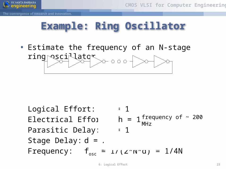
Example: Ring Oscillator
• Estimate the frequency of an N-stage ring oscillator
Logical Effort: g = 1
Electrical Effort: h = 1
Parasitic Delay: p = 1
Stage Delay: d = 2
Frequency: fosc = 1/(2*N*d) = 1/4N
31 stage ring oscillator in 0.6 mm process has frequency of ~ 200 MHz

CMOS VLSI for Computer Engineering
6: Logical Effort 24
Example: FO4 Inverter
• Estimate the delay of a fanout-of-4 (FO4) inverter
Logical Effort: g = 1
Electrical Effort: h = 4
Parasitic Delay: p = 1
Stage Delay: d = 5
d
The FO4 delay is about
300 ps in 0.6 mm process
15 ps in a 65 nm process

CMOS VLSI for Computer Engineering
Optimal Delay
The optimum delay is obtained when
€
∂tdelay∂C i
gate
= 0
Collect terms due to C igate and differentiate
€
∂∂C i
gate
gi−1Cgatei
γCgatei−1
+giCgate
i+1
γCgatei
⎛
⎝ ⎜ ⎜
⎞
⎠ ⎟ ⎟= 0
€
tdelay = tp0 pi +C i+1
gate
C igate
C igate
Cint−inv
⎛
⎝ ⎜
⎞
⎠ ⎟
i=1
N
∑
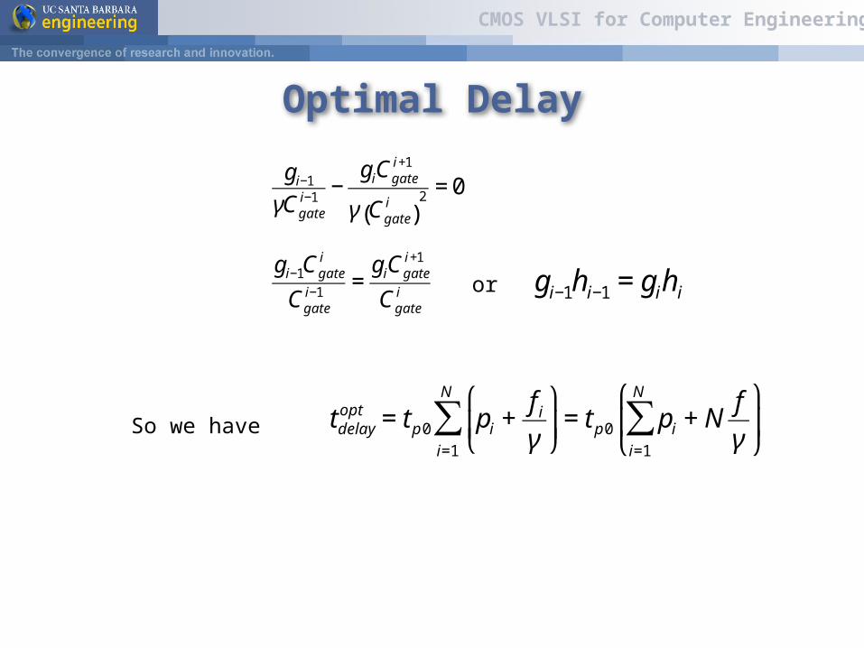
CMOS VLSI for Computer Engineering
€
gi−1
γCgatei−1
−giCgate
i+1
γ Cgatei
( )2 = 0
€
gi−1Cgatei
Cgatei−1
=giCgate
i+1
Cgatei or
€
gi−1hi−1 = gihi
So we have
€
tdelayopt = tp0 pi +
f iγ
⎛
⎝ ⎜
⎞
⎠ ⎟
i=1
N
∑ = t p0 pi + Nf
γi=1
N
∑ ⎛
⎝ ⎜
⎞
⎠ ⎟
Optimal Delay

CMOS VLSI for Computer Engineering
6: Logical Effort 27
If γ=1
Designing Fast Circuits
• Delay is smallest when each stage bears same effort
• Thus minimum delay of N stage path is
• This is a key result of logical effort Find fastest possible delay Doesn’t require calculating gate sizes
i FD d D P
1ˆ Ni if g h F
1ND NF P

CMOS VLSI for Computer Engineering
6: Logical Effort 28
Gate Sizes
• How wide should the gates be for least delay?
• Working backward, apply capacitance transformation to find input capacitance of each gate given load it drives.
• Check work by verifying input cap spec is met.
ˆ
ˆ
out
in
i
i
CC
i outin
f gh g
g CC
f

CMOS VLSI for Computer Engineering
6: Logical Effort 29
Multistage Logic Networks
• Logical effort generalizes to multistage networks
• Path Logical Effort
• Path Electrical Effort
• Path Effort
iG gout-path
in-path
CH
C
i i iF f g h 10
x y z20
g1 = 1h
1 = x/10
g2 = 5/3h
2 = y/x
g3 = 4/3h
3 = z/y
g4 = 1h
4 = 20/z

CMOS VLSI for Computer Engineering
6: Logical Effort 30
Multistage Logic Networks
• Logical effort generalizes to multistage networks
• Path Logical Effort
• Path Electrical Effort
• Path Effort
• Can we write F = GH?
iG gout path
in path
CH
C
i i iF f g h
CMOS VLSI for Computer Engineering
6: Logical Effort 31
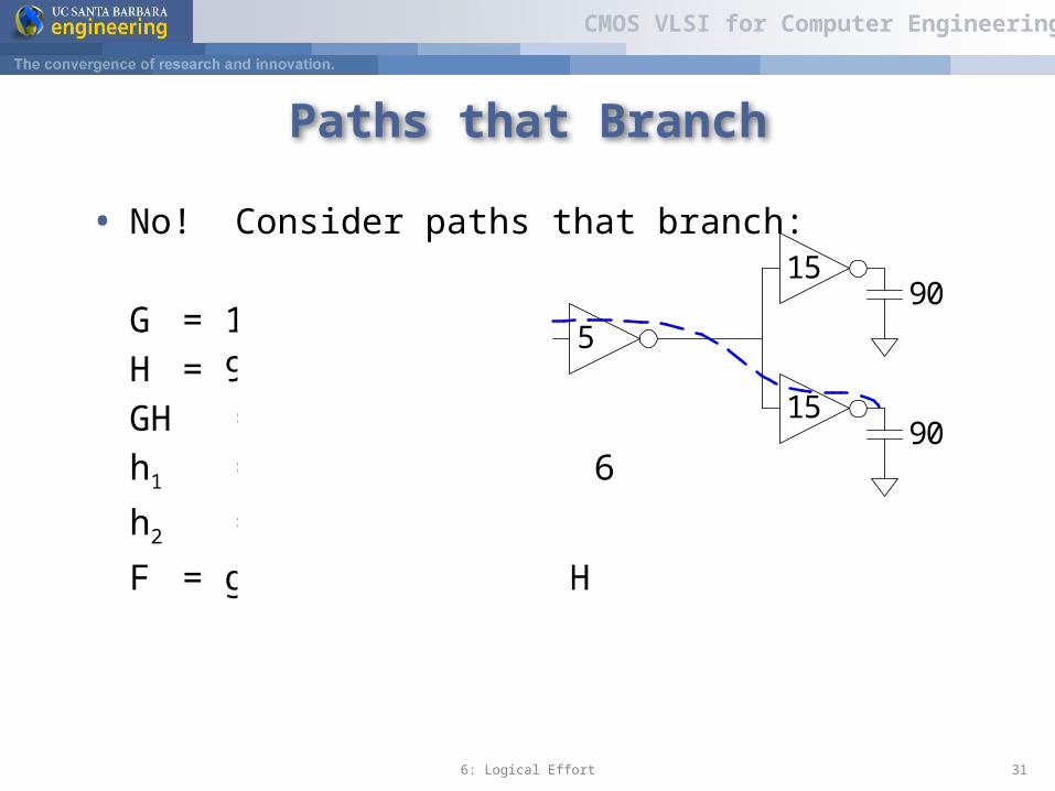
Paths that Branch
• No! Consider paths that branch:
G = 1
H = 90 / 5 = 18
GH = 18
h1 = (15 +15) / 5 = 6
h2 = 90 / 15 = 6
F = g1g2h1h2 = 36 = 2GH
5
15
1590
90
CMOS VLSI for Computer Engineering
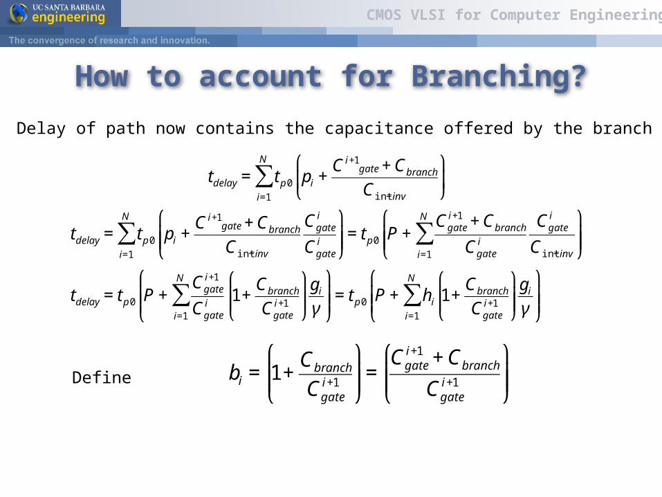
How to account for Branching?
€
tdelay = tp0 pi +C i+1
gate +Cbranch
Cint−inv
⎛
⎝ ⎜
⎞
⎠ ⎟
i=1
N
∑
Delay of path now contains the capacitance offered by the branch
€
tdelay = tp0 pi +C i+1
gate +Cbranch
Cint−inv
Cgatei
Cgatei
⎛
⎝ ⎜ ⎜
⎞
⎠ ⎟ ⎟
i=1
N
∑ = t p0 P +Cgate
i+1 +Cbranch
Cgatei
Cgatei
Cint−invi=1
N
∑ ⎛
⎝ ⎜ ⎜
⎞
⎠ ⎟ ⎟
tdelay = tp0 P +Cgate
i+1
Cgatei
1+Cbranch
Cgatei+1
⎛
⎝ ⎜ ⎜
⎞
⎠ ⎟ ⎟gi
γi=1
N
∑ ⎛
⎝ ⎜ ⎜
⎞
⎠ ⎟ ⎟= t p0 P + hi 1+
Cbranch
Cgatei+1
⎛
⎝ ⎜ ⎜
⎞
⎠ ⎟ ⎟gi
γi=1
N
∑ ⎛
⎝ ⎜ ⎜
⎞
⎠ ⎟ ⎟
Define
€
bi = 1+Cbranch
Cgatei+1
⎛
⎝ ⎜ ⎜
⎞
⎠ ⎟ ⎟=
Cgatei+1 +Cbranch
Cgatei+1
⎛
⎝ ⎜ ⎜
⎞
⎠ ⎟ ⎟

CMOS VLSI for Computer Engineering
Branching effort
€
tdelay = tp0 P + gibihi
i=1
N
∑ ⎛
⎝ ⎜
⎞
⎠ ⎟

CMOS VLSI for Computer Engineering
6: Logical Effort 34
Branching Effort
• Introduce branching effort Accounts for branching between stages in path
• Now we compute the path effort F = GBH
on path off path
on path
C Cb
C
iB bih BH
Note:

CMOS VLSI for Computer Engineering
6: Logical Effort 35
Example: 3-stage path
• Select gate sizes x and y for least delay from A to B
8 x
x
x
y
y
45
45
A
B

CMOS VLSI for Computer Engineering
6: Logical Effort 36
Example: 3-stage path
Logical Effort G = (4/3)*(5/3)*(5/3) = 100/27
Electrical Effort H = 45/8
Branching Effort B = 3 * 2 = 6
Path Effort F = GBH = 125
Best Stage Effort
Parasitic Delay P = 2 + 3 + 2 = 7
Delay D = 3*5 + 7 = 22 = 4.4 FO4
8 x
x
x
y
y
45
45
A
B
3ˆ 5f F

CMOS VLSI for Computer Engineering
6: Logical Effort 37
Example: 3-stage path
• Work backward for sizes
y = 45 * (5/3) / 5 = 15
x = (15*2) * (5/3) / 5 = 10
P: 4N: 4
45
45
A
BP: 4N: 6
P: 12N: 3
8 x
x
x
y
y
45
45
A
B

CMOS VLSI for Computer Engineering
6: Logical Effort 38
Best Number of Stages
• How many stages should a path use? Minimizing number of stages is not always fastest
• Example: drive 64-bit datapath with unit inverter
D = NF1/N + P
= N(64)1/N + N
1 1 1 1
8 4
16 8
2.8
23
64 64 64 64
Initial Driver
Datapath Load
N:f:D:
16465
2818
3415
42.815.3
Fastest

CMOS VLSI for Computer Engineering
6: Logical Effort 39
Derivation
• Consider adding inverters to end of path How many give least delay?
• Define best stage effort
N - n1 Extra Inverters
Logic Block:n
1 Stages
Path Effort F 11
11
N
n
i invi
D NF p N n p
1 1 1
ln 0N N Ninv
DF F F p
N
1 ln 0invp
1NF

CMOS VLSI for Computer Engineering
6: Logical Effort 40
Best Stage Effort
• has no closed-form solution
• Neglecting parasitics (pinv = 0), we find r = 2.718 (e)
• For pinv = 1, solve numerically for r = 3.59
1 ln 0invp

CMOS VLSI for Computer Engineering
6: Logical Effort 41
Sensitivity Analysis
• How sensitive is delay to using exactly the best number of stages?
• 2.4 < r < 6 gives delay within 15% of optimal We can be sloppy! I like r = 4
1.0
1.2
1.4
1.6
1.0 2.00.5 1.40.7
N / N
1.151.26
1.51
( =2.4)(=6)
D(N
) /D
(N)
0.0
CMOS VLSI for Computer Engineering
6: Logical Effort 42
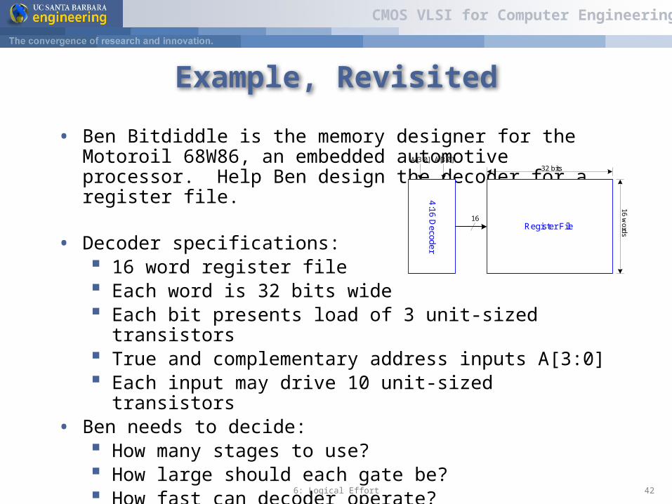
Example, Revisited
• Ben Bitdiddle is the memory designer for the Motoroil 68W86, an embedded automotive processor. Help Ben design the decoder for a register file.
• Decoder specifications: 16 word register file Each word is 32 bits wide Each bit presents load of 3 unit-sized transistors True and complementary address inputs A[3:0] Each input may drive 10 unit-sized transistors
• Ben needs to decide: How many stages to use? How large should each gate be? How fast can decoder operate?
A[3:0] A[3:0]
16
32 bits
16 wo
rds
4:16 Decoder
Register File
CMOS VLSI for Computer Engineering
6: Logical Effort 43
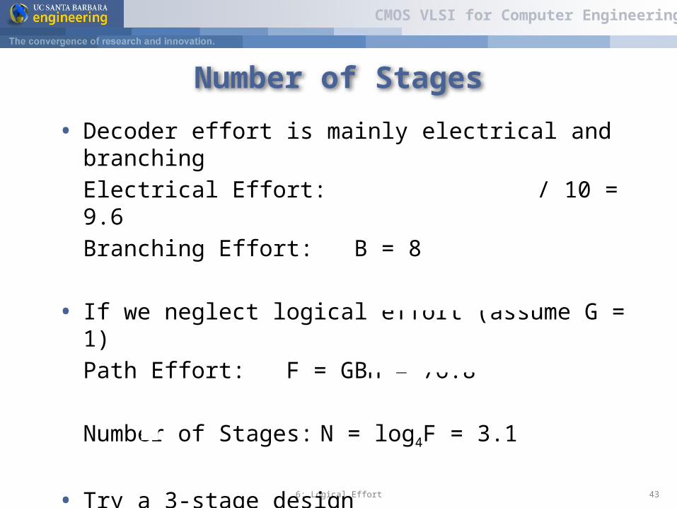
Number of Stages
• Decoder effort is mainly electrical and branching
Electrical Effort: H = (32*3) / 10 = 9.6
Branching Effort: B = 8
• If we neglect logical effort (assume G = 1)
Path Effort: F = GBH = 76.8
Number of Stages: N = log4F = 3.1
• Try a 3-stage design

CMOS VLSI for Computer Engineering
6: Logical Effort 44
Gate Sizes & Delay
Logical Effort: G = 1 * 6/3 * 1 = 2
Path Effort: F = GBH = 154
Stage Effort:
Path Delay:
Gate sizes: z = 96*1/5.36 = 18 y = 18*2/5.36 = 6.7A[3] A[3] A[2] A[2] A[1] A[1] A[0] A[0]
word[0]
word[15]
96 units of wordline capacitance
10 10 10 10 10 10 10 10
y z
y z
1/3ˆ 5.36f F ˆ3 1 4 1 22.1D f
CMOS VLSI for Computer Engineering
6: Logical Effort 45
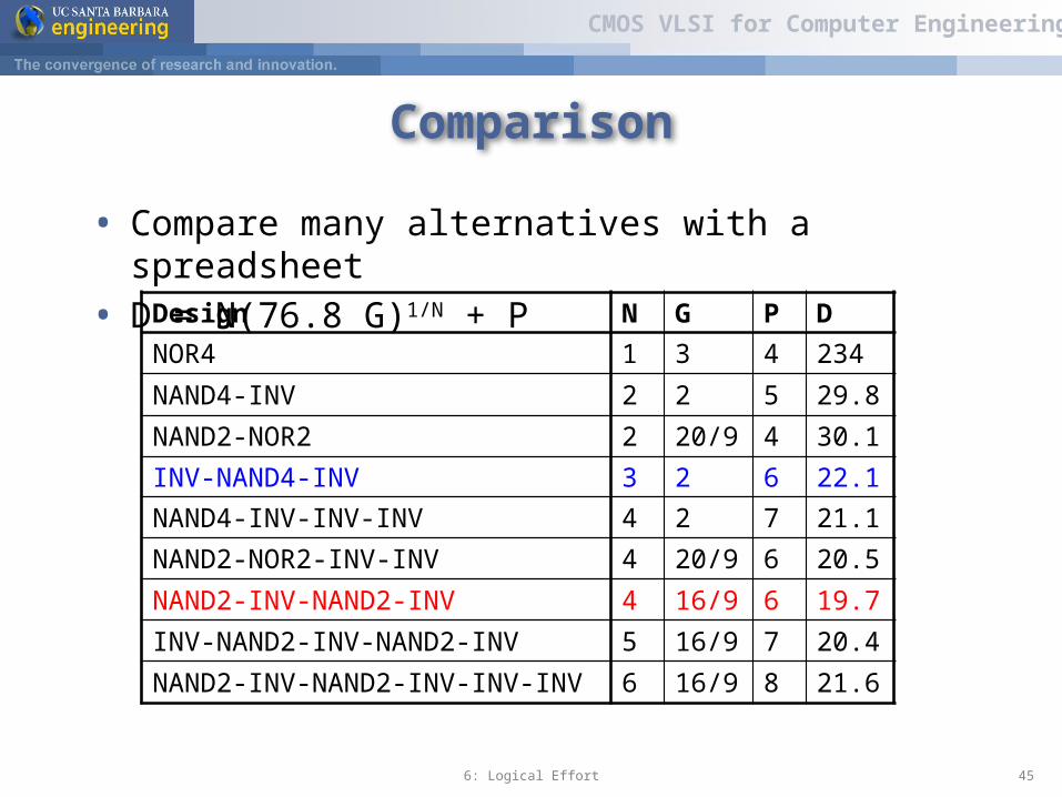
Comparison
• Compare many alternatives with a spreadsheet
• D = N(76.8 G)1/N + PDesign N G P DNOR4 1 3 4 234
NAND4-INV 2 2 5 29.8
NAND2-NOR2 2 20/9 4 30.1
INV-NAND4-INV 3 2 6 22.1NAND4-INV-INV-INV 4 2 7 21.1
NAND2-NOR2-INV-INV 4 20/9 6 20.5
NAND2-INV-NAND2-INV 4 16/9 6 19.7
INV-NAND2-INV-NAND2-INV 5 16/9 7 20.4
NAND2-INV-NAND2-INV-INV-INV 6 16/9 8 21.6

CMOS VLSI for Computer Engineering
6: Logical Effort 46
Review of Definitions
Term Stage Path
number of stages
logical effort
electrical effort
branching effort
effort
effort delay
parasitic delay
delay
iG g out-path
in-path
C
CH
N
iB b F GBH
F iD f
iP p i FD d D P
out
in
CCh
on-path off-path
on-path
C C
Cb
f gh
f
p
d f p
g
1

CMOS VLSI for Computer Engineering
6: Logical Effort 47
Method of Logical Effort
1) Compute path effort
2) Estimate best number of stages
3) Sketch path with N stages
4) Estimate least delay
5) Determine best stage effort
6) Find gate sizes
F GBH
4logN F
1ND NF P
1ˆ Nf F
ˆi
i
i outin
g CC
f

CMOS VLSI for Computer Engineering
6: Logical Effort 48
Limits of Logical Effort
• Chicken and egg problem Need path to compute G But don’t know number of stages without G
• Simplistic delay model Neglects input rise time effects
• Interconnect Iteration required in designs with wire
• Maximum speed only Not minimum area/power for constrained delay

CMOS VLSI for Computer Engineering
6: Logical Effort 49
Summary
• Logical effort is useful for thinking of delay in circuits Numeric logical effort characterizes gates NANDs are faster than NORs in CMOS Paths are fastest when effort delays are ~4 Path delay is weakly sensitive to stages, sizes But using fewer stages doesn’t mean faster paths Delay of path is about log4F FO4 inverter delays
Inverters and NAND2 best for driving large caps
• Provides language for discussing fast circuits But requires practice to master


![EE415 VLSI Design THE INVERTER [Adapted from Rabaey’s Digital Integrated Circuits, ©2002, J. Rabaey et al.]](https://img.dokumen.tips/doc/110x75/56649ea35503460f94ba7dea/ee415-vlsi-design-the-inverter-adapted-from-rabaeys-digital-integrated.jpg)

![EE415 VLSI Design DYNAMIC LOGIC [Adapted from Rabaey’s Digital Integrated Circuits, ©2002, J. Rabaey et al.]](https://img.dokumen.tips/doc/110x75/56649e665503460f94b61057/ee415-vlsi-design-dynamic-logic-adapted-from-rabaeys-digital-integrated.jpg)


![EE415 VLSI Design The Devices: Diode [Adapted from Rabaey’s Digital Integrated Circuits, ©2002, J. Rabaey et al.]](https://img.dokumen.tips/doc/110x75/56649dca5503460f94ac0749/ee415-vlsi-design-the-devices-diode-adapted-from-rabaeys-digital-integrated.jpg)
![EE414 VLSI Design Introduction Introduction to VLSI Design [Adapted from Rabaey’s Digital Integrated Circuits, ©2002, J. Rabaey et al.]](https://img.dokumen.tips/doc/110x75/56649db25503460f94aa0d37/ee414-vlsi-design-introduction-introduction-to-vlsi-design-adapted-from-rabaeys.jpg)
![EE415 VLSI Design COMBINATIONAL LOGIC [Adapted from Rabaeys Digital Integrated Circuits, ©2002, J. Rabaey et al.]](https://img.dokumen.tips/doc/110x75/5519b7875503465b578b4854/ee415-vlsi-design-combinational-logic-adapted-from-rabaeys-digital-integrated-circuits-2002-j-rabaey-et-al.jpg)


