Embed Size (px)
Citation preview

CMOS Analog Design Using All-Region MOSFET Modeling
1
CMOS Analog Design Using All-Region MOSFET Modeling
Chapter 2
Advanced MOS transistor modeling

CMOS Analog Design Using All-Region MOSFET Modeling
2
Semiconductors Four types of charge are present inside a
semiconductor: the fixed positive charge of ionized donors, the fixed negative charge of ionized acceptors, the positive mobile charge of holes, and the negative mobile charge of electrons.
We consider all donors and acceptors ionized
On this basis, the net positive charge density ρ is
and D D A AN N N N
( )D Aq N N p n
CMOS Analog Design Using All-Region MOSFET Modeling
3
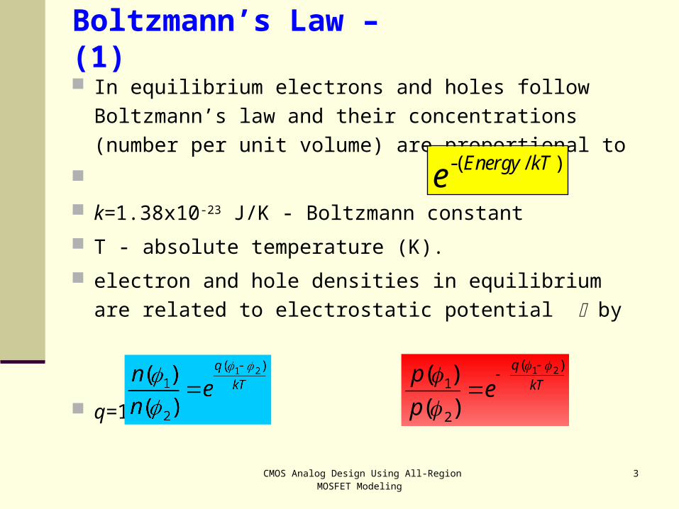
Boltzmann’s Law – (1)
In equilibrium electrons and holes follow Boltzmann’s
law and their concentrations (number per unit
volume) are proportional to
k=1.38x10⁻²³ J/K - Boltzmann constant
T - absolute temperature (K).
electron and hole densities in equilibrium are related
to electrostatic potential by
q=1.6x10⁻¹⁹ C
-( / )Energy kTe
1 2( )1
2
( )
( )
q
kTp
ep
CMOS Analog Design Using All-Region MOSFET Modeling
4
n0 and p0 - equilibrium electron and hole concentrations
in the neutral bulk (=0 )
- normalized electrostatic potential
- thermal voltage
the mass-action law is
ni - concentration of electrons (and holes) in the intrinsic
semiconductor
2inp n
0 0
qukTp p e p e
0 0
qukTn n e n e
/ tu /t kT q
Boltzmann’s Law – (2)

CMOS Analog Design Using All-Region MOSFET Modeling
5
Example: Calculate the built-in potential for a Si p-n junction with NA = 1017 atoms/cm3 and ND = 1018 atoms/cm3 ,T=300K
In equilibrium, if we choose the potential origin = 0 where the
semiconductor is intrinsic (i.e., where p0=n0=ni), then/
0t
ip n e /0
tin n e
Far from the junction in the n-side
Far from the junction in the p-side
/0
n region t
D in N n e /
0p region t
A ip N n e
The built-in potential is given by
2ln ln lnD A D A
bi n region p region t t ti i i
N N N N
n n n
1526 ln 10 900 mVbi
CMOS Analog Design Using All-Region MOSFET Modeling
6
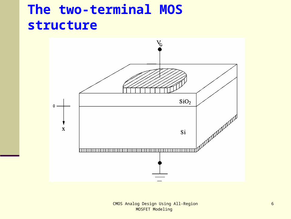
The two-terminal MOS structure

CMOS Analog Design Using All-Region MOSFET Modeling
7
The ideal two-terminal MOS structure (VFB=0)
CG s
ox
QV
C
oxox
ox
AC
t
; G ox oxG ox
ox
Q CQ C
A A t
A - capacitor area,
tox - oxide thickness
ox - permittivity of oxide
M
O
S+
s
_
GG s
ox
QV
C
CQ
GQ
0G CQ Q
GV

CMOS Analog Design Using All-Region MOSFET Modeling
8
Example: oxide capacitance
(a) Calculate the oxide capacitance per unit area for tox= 5
and 20 nm assuming ox = 3.90, where 0= 8.85·10-14
F/cm is the permittivity of free space. (b) Determine the
area of a 1pF metal-oxide-metal capacitor for the two
oxide thicknesses given in (a).
Answer: (a) =690 nF/cm2 = 6.9 fF/m2 for tox=5 nm and =
172 nF/cm2= 1.7 fF/m2 for tox= 20 nm. The capacitor
areas are 145 and 580 m2 for oxide thicknesses of 5
and 20 nm, respectively.
CMOS Analog Design Using All-Region MOSFET Modeling
9
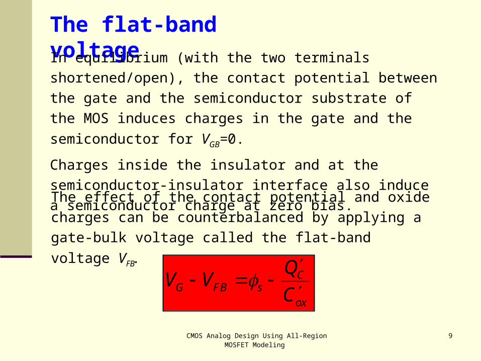
The flat-band voltage
In equilibrium (with the two terminals shortened/open), the
contact potential between the gate and the semiconductor
substrate of the MOS induces charges in the gate and the
semiconductor for VGB=0.
Charges inside the insulator and at the semiconductor-insulator
interface also induce a semiconductor charge at zero bias.
The effect of the contact potential and oxide charges can be
counterbalanced by applying a gate-bulk voltage called the
flat-band voltage VFB.
CG FB s
ox
QV V
C
CMOS Analog Design Using All-Region MOSFET Modeling
10
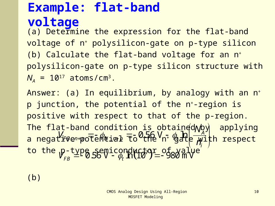
Example: flat-band voltage(a) Determine the expression for the flat-band voltage of n+
polysilicon-gate on p-type silicon (b) Calculate the flat-band voltage
for an n+ polysilicon-gate on p-type silicon structure with NA = 1017
atoms/cm3.
Answer: (a) In equilibrium, by analogy with an n+ p junction, the
potential of the n+-region is positive with respect to that of the p-
region. The flat-band condition is obtained by applying a negative
potential to the n+ gate with respect to the p-type semiconductor of
value
(b)
_ _ 0.56 V ln AFB n p bi n p t
i
NV
n
70.56 V ln 10 980 mVFB tV

CMOS Analog Design Using All-Region MOSFET Modeling
11
Regions of operation of the MOSFET:
Accumulation (p-substrate)
Holes + accumulate in the p-type semiconductor surface
0
0
GB FB
C
s
V V
Q
+ + + + + + + + + + + + + +VGB
G
B
- - - - - - - - - - -
+ + + +Qo
QG
QC

CMOS Analog Design Using All-Region MOSFET Modeling
12
VGB
G
B
+ + + + + + + + +
+ + + +Qo
QG
-- - -- -- -
-QC- -- --
F = Fermi potential ( to be defined)
0
0
GB FB
C
s F
V V
Q
Holes evacuate from the P
semiconductor surface and
acceptor ion charges
become uncovered-
Regions of operation of the MOSFET:
Depletion (p-substrate)

CMOS Analog Design Using All-Region MOSFET Modeling
13
VGB
G
B
+ + + + + + + + +
+ + + +Qo
QG
-- - -- -- --
QC- -- ---- - - - - -
--
0GB FB
C
s F
V V
Q
electrons approach the surface!
Regions of operation of the MOSFET:
Inversion (p-substrate)

CMOS Analog Design Using All-Region MOSFET Modeling
14
Inversion for p-type substrate
Volume charge density inside the semiconductor:
Depletion of holes prevails over electron charge when
or, equivalently
0 0 0 0( )u uq p e n e n p
0 0u up e n e
0
0
ln( )2
t p
n
For >F the concentration of minority carriers (n)
becomes higher than that of majority carriers (p); the
semiconductor operates in the inversion region
20 02
ln( ) ln( )2
tt F
i i
p p
n n
mass-action law
CMOS Analog Design Using All-Region MOSFET Modeling
15
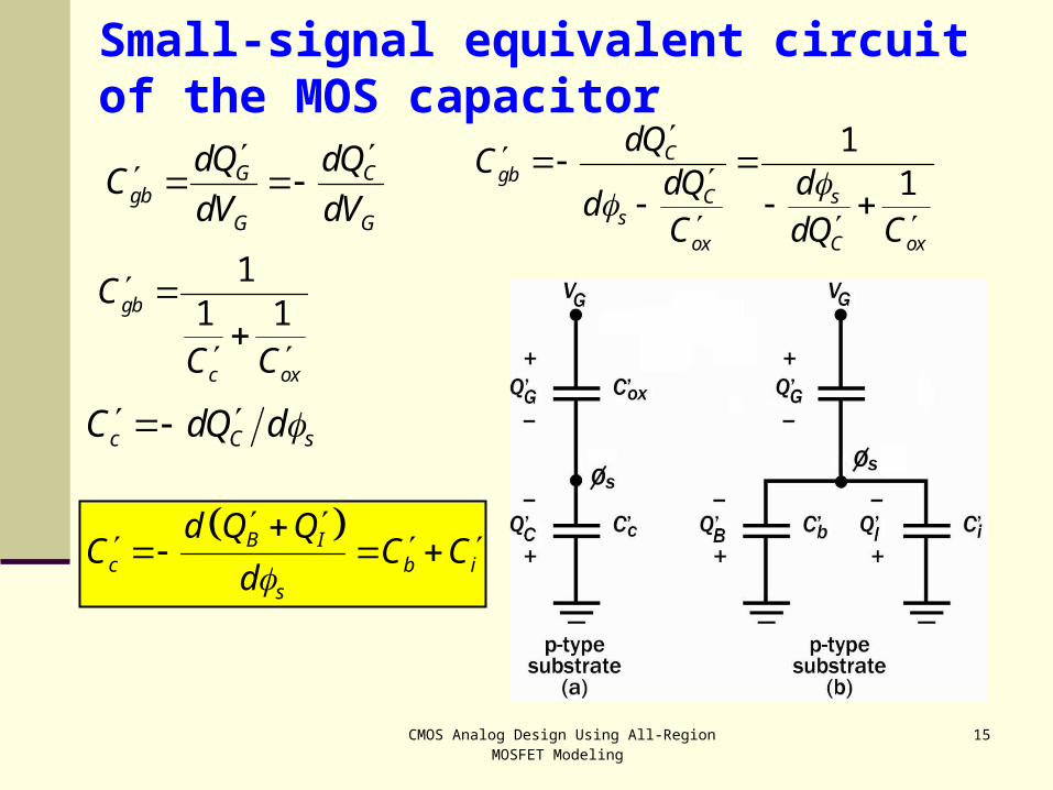
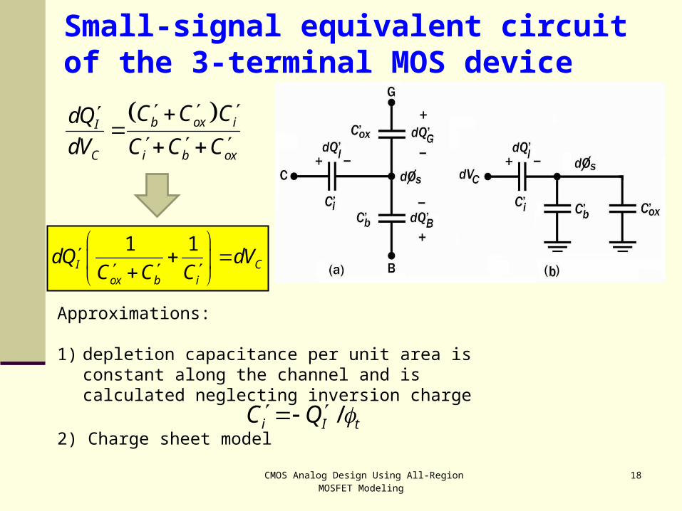
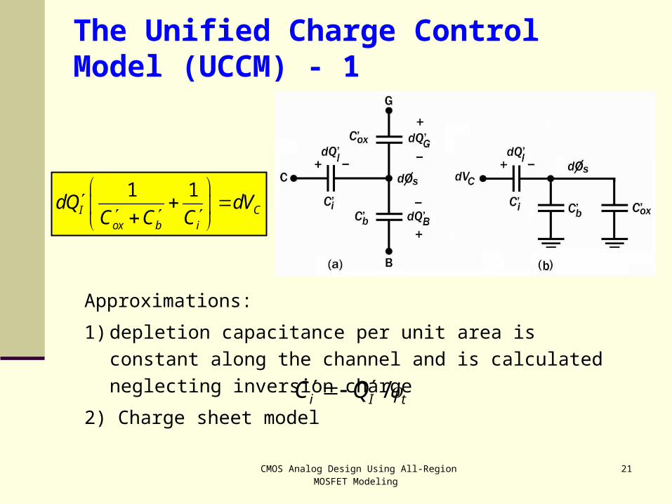
Small-signal equivalent circuit of the MOS capacitor
G Cgb
G G
dQ dQC
dV dV
11
Cgb
C ss
ox C ox
dQC
dQ dd
C dQ C
11 1gb
c ox
C
C C
c C sC dQ d
B Ic b i
s
d Q QC C C
d
CMOS Analog Design Using All-Region MOSFET Modeling
16
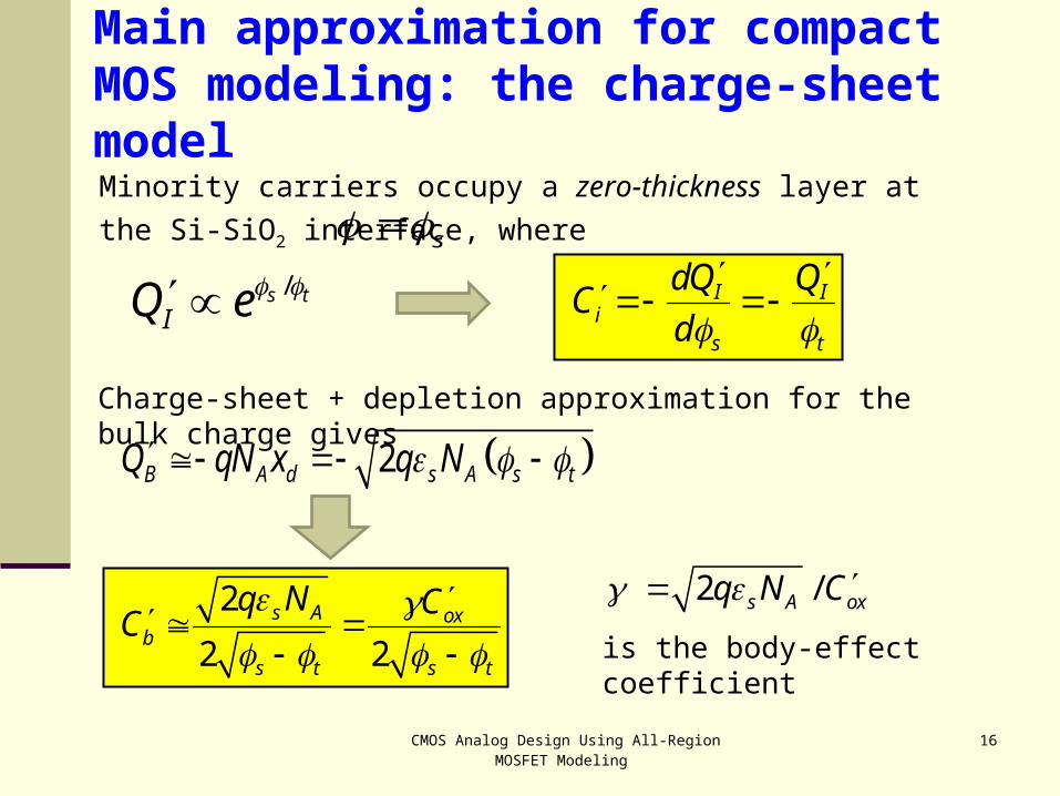
Main approximation for compact MOS modeling: the charge-sheet model
Minority carriers occupy a zero-thickness layer at the Si-SiO2
interface, where
/s tIQ e
s
I Ii
s t
dQ QC
d
Charge-sheet + depletion approximation for the bulk charge gives
2 B A d s A s tQ qN x q N
2
2 2s A ox
b
s t s t
q N CC
2 /s A oxq N C
is the body-effect coefficient

CMOS Analog Design Using All-Region MOSFET Modeling
17
The three-terminal MOS structure
The origin of potential is taken deep in the bulk
n+ p
VGVC Carrier concentrations in Si
substrate follow Boltzmann’s
law:
n, p exp(-Energy/kT)
( )
0 0 0 0; C
C
q Vqu uukT kTp p e p e n n e n e
/2 2C C tu Vi ipn n e n e
electrons are no longer in equilibrium with holes due to the bias of
the source-bulk junction VC
CMOS Analog Design Using All-Region MOSFET Modeling
18
b ox iI
C i b ox
C C CdQ
dV C C C
1 1I C
ox b i
dQ dVC C C
Approximations:
1) depletion capacitance per unit area is constant along the channel and is calculated neglecting inversion charge
2) Charge sheet model /i I tC Q
Small-signal equivalent circuit of the 3-terminal MOS device
CMOS Analog Design Using All-Region MOSFET Modeling
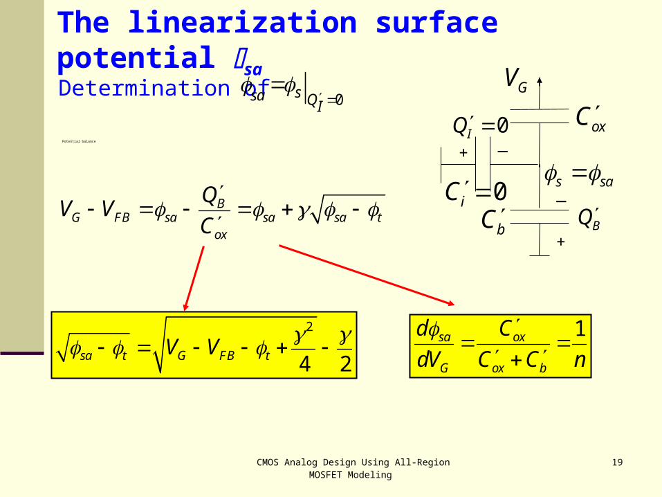
19
Determination of
Potential balance
0ssa QI
1sa ox
G ox b
d C
dV C C n
2
4 2sa t G FB tV V
The linearization surface potential sa
BG FB sa sa sa t
ox
QV V
C
GV
s sa
BQ
+ _
bC+
_
0IQ
0iC
oxC

CMOS Analog Design Using All-Region MOSFET Modeling
20
Example: slope factor
For tox = 5 nm and 20 nm determine the minimum doping NA for
which the slope factor n < 1.25 at sa = 2F.
Answer: For sa=2F
Thus, for n=1.25
where F is a weak (logarithmic) function of NA. Using 2F = 0.8 V
for the first calculation, we obtain after two iterations that NA>
4.9x10¹⁵ atoms/cm3 for tox=5nm, and NA > 2.3·1014 atoms/cm3 for
tox=20 nm.
2 2 =1+ 1 1
2 2 2s A s Ab
ox ox sa ox F
q N q NCn
C C C
2 20.25 2 4 =
2F ox
As
CN
q
CMOS Analog Design Using All-Region MOSFET Modeling
21
The Unified Charge Control Model (UCCM) - 1
1 1I C
ox b i
dQ dVC C C
Approximations:
1) depletion capacitance per unit area is constant along the
channel and is calculated neglecting inversion charge
2) Charge sheet model /i I tC Q

CMOS Analog Design Using All-Region MOSFET Modeling
22
The Unified Charge Control Model (UCCM) - 2
1 1I C
ox b i
dQ dVC C C
/i I tC Q
1 tI C
ox I
dQ dVnC Q
1 bGB
ox
Cn n V
C
where
Integrating from an arbitrary channel potential VC to a reference
potential VP yields the unified charge control model (UCCM)
lnIP I IP C t
ox t IP
Q Q QV V
nC Q
C P
IP I V VQ Q
CMOS Analog Design Using All-Region MOSFET Modeling
23
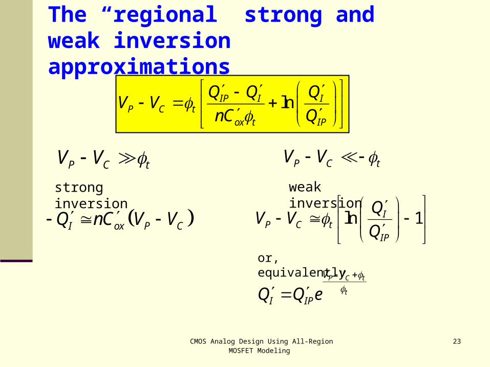
The “regional” strong and weak inversion approximations
lnIP I IP C t
ox t IP
Q Q QV V
nC Q
I ox P CQ nC V V
P C tV V P C tV V
ln 1IP C t
IP
QV V
Q
or, equivalently
P C t
t
V V
I IPQ Q e
strong inversion weak inversion
CMOS Analog Design Using All-Region MOSFET Modeling
24
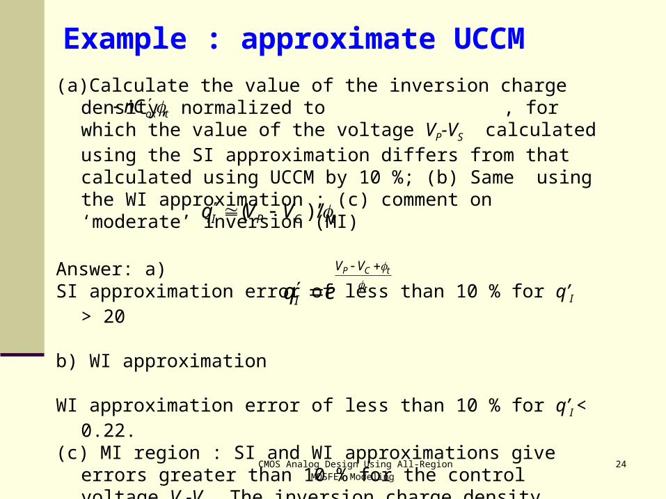
Example : approximate UCCM
(a)Calculate the value of the inversion charge density, normalized to , for which the value of the voltage VP-VS calculated using the SI approximation differs from that calculated using UCCM by 10 %; (b) Same using the WI approximation ; (c) comment on ‘moderate’ inversion (MI)
Answer: a) SI approximation error of less than 10 % for q’I > 20
b) WI approximation WI approximation error of less than 10 % for q’I < 0.22.(c) MI region : SI and WI approximations give errors greater than
10 % for the control voltage VP-VS. The inversion charge density variation from the lower to the upper limit of the MI region is approximately two orders of magnitude (20/0.22).
ox tnC
( ) /I P C tq V V
P C t
t
V V
Iq e
CMOS Analog Design Using All-Region MOSFET Modeling
25
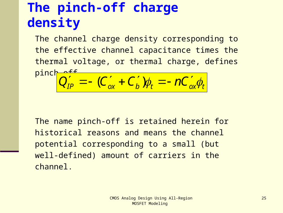
The pinch-off charge density
The channel charge density corresponding to the effective
channel capacitance times the thermal voltage, or thermal
charge, defines pinch-off
( )IP ox b t ox tQ C C nC
The name pinch-off is retained herein for historical reasons
and means the channel potential corresponding to a small
(but well-defined) amount of carriers in the channel.

CMOS Analog Design Using All-Region MOSFET Modeling
26
The pinch-off voltage VP
The channel-to-substrate voltage (VC) for which the channel
charge density equals is called the pinch-off voltage VP.
UCCM is
asymptotically correct
in weak inversion if
in weak
inversion
2 / 2 /( 1)sa F C t sa F C tV VI b t ox tQ C e C n e
2P sa FV
2 1 ln1P sa F t
nV
n

CMOS Analog Design Using All-Region MOSFET Modeling
27
Threshold voltage
Equilibrium threshold voltage VT0, for VC=0:
Gate voltage for which
or
Gate voltage for which VP=0
2P sa FV
G FB sa ox sa tV V C Recalling that
0 2 2 T FB F FV V it follows that
I IP ox tQ Q nC

CMOS Analog Design Using All-Region MOSFET Modeling
28
Example: threshold voltage
Estimate VT0 for an n-channel transistor with n+ polysilicon gate,
NA=1017 atoms/cm3 and tox=5 nm.
Answer: The flat-band voltage (slide 10) is -0.98 V; F=0.419; C’ox=
690 nF/cm2. The body-effect factor is
For this low value of the threshold voltage, the off-current (for VGS=0)
is too high for digital circuits.
Solution to control the magnitude of the threshold voltage without an
exaggerated increase in the slope factor a non-uniform
high-low channel doping.
2 / 0.264 Vs A oxq N C
0 2 2 = 0.98 0.838 0.264 0.838= 0.1VT FB F FV V

CMOS Analog Design Using All-Region MOSFET Modeling
29
nVV
V 0TGBP
Pinch-off voltage vs. gate voltage
Useful approximation:
-1.00E+00
0.00E+00
1.00E+00
2.00E+00
3.00E+00
4.00E+00
0.00E+00 1.00E+00 2.00E+00 3.00E+00 4.00E+00 5.00E+00 6.00E+00
pin
ch-off v
oltage
0
0.5
1
1.5
2
slo
pe fa
cto
r
4.0
3.0
2.0
1.0
0
-1.0
0 1.0 2.0 3.0 4.0 5.0
2.0
1.5
1.0
0.5
0
VG (V)
VP
VT0 (equilibrium threshold voltage)
1sa oxP
G G b ox
d CdV
dV dV C C n
CMOS Analog Design Using All-Region MOSFET Modeling
30
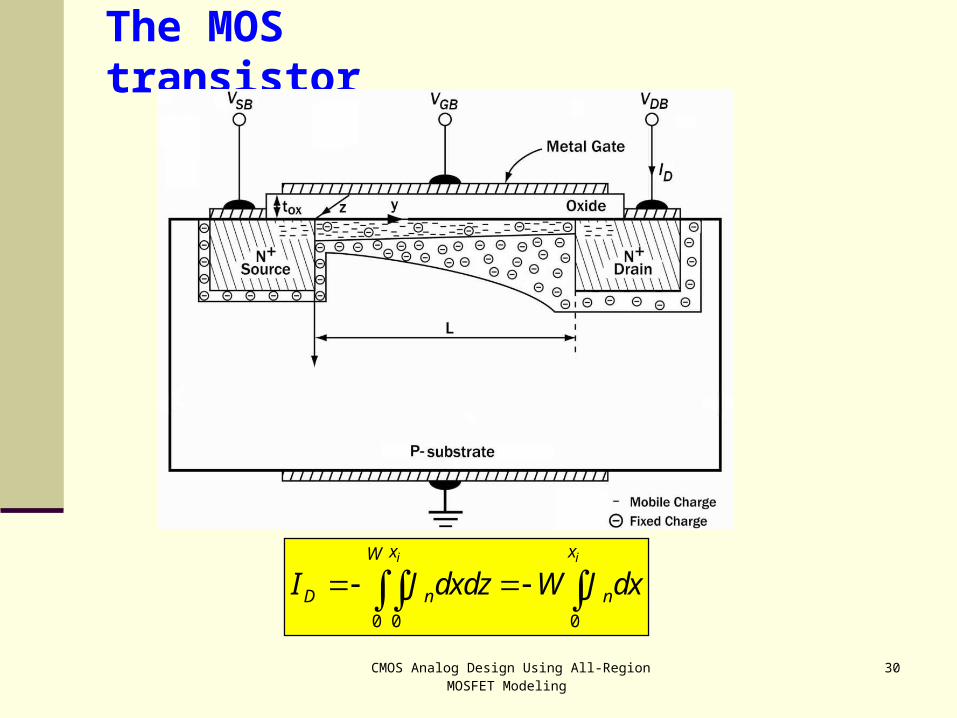
The MOS transistor
0 0 0
i ix xW
D n nI J dxdz W J dx
CMOS Analog Design Using All-Region MOSFET Modeling
31
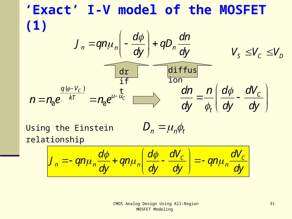
‘Exact’ I-V model of the MOSFET (1)
n nn
d dnJ qn qD
dy dy
( )
0 0
C
C
q Vu ukTn n e n e
C
t
dVdn n d
dy dy dy
Using the Einstein relationship n n tD
C Cn n n n
dV dVd dJ qn qn qn
dy dy dy dy
S C DV V V
drift diffusion
CMOS Analog Design Using All-Region MOSFET Modeling
32
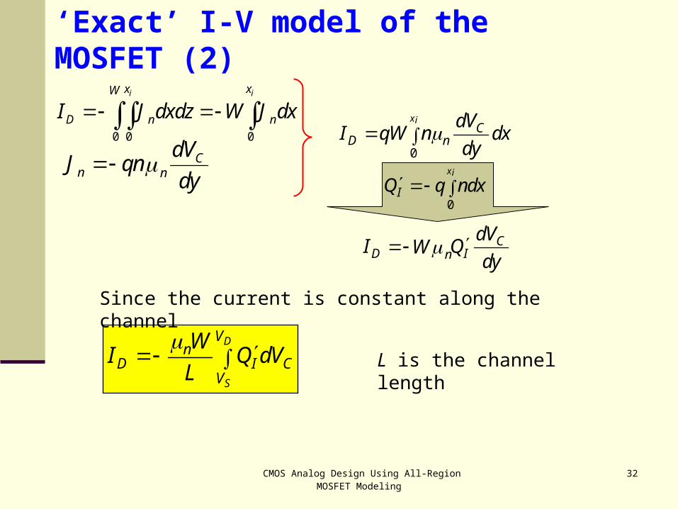
0 0 0
i ix xW
D n nI J dxdz W J dx 0
xiC
D ndV
I qW n dxdy
C
n n
dVJ qn
dy
0
xi
IQ q ndx
D
S
Vn
D I CV
WI Q dV
L
L is the channel length
Since the current is constant along the channel
‘Exact’ I-V model of the MOSFET (2)
CD In
dVI QW
dy

CMOS Analog Design Using All-Region MOSFET Modeling
33
IC s t
I
dQdV d
Q
I i C sdQ C dV d
CdVsd
GVI
it
QC
IdQ+ _
Charge-sheet formula for the current
s ID drift diff n I n t
d dQI I I WQ W
dy dy
Cn n
dVJ qn
dy

CMOS Analog Design Using All-Region MOSFET Modeling
34
Charge control compact model (1)
sd
BdQ
+ _
GV
bC +
_
IdQ
iC
oxCCdV ( )I ox b s ox sdQ C C d nC d
s ID n I n t
d dQI WQ W
dy dy
( )n ID I t ox
ox
W dQI Q nC
nC dy
Integrating along the channel yields
2 2
2n IS ID
D t IS IDox
W Q QI Q Q
L nC

CMOS Analog Design Using All-Region MOSFET Modeling
35
2 2
2 2n IS ID IS ID IS ID
D t IS ID ox tnox ox
W Q Q Q Q Q QI Q Q W nC
L nC nC L
drift + diffusion
0
2IS ID s sL
D ox tn
Q QI W nC
L
average charge density
average electric field
“virtual” charge
Charge control compact model (2)
I ox sdQ nC d
CMOS Analog Design Using All-Region MOSFET Modeling
36
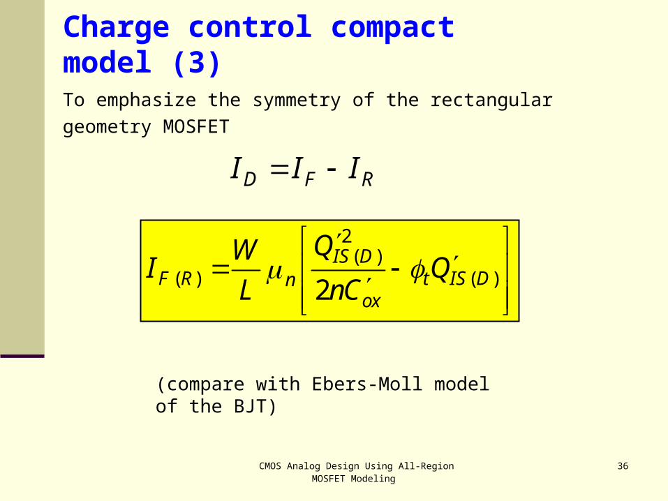
To emphasize the symmetry of the rectangular geometry
MOSFET
D F RI I I
2( )
( ) ( )2IS D
F R t IS Dnox
QWI Q
L nC
(compare with Ebers-Moll model of the BJT)
Charge control compact model (3)

CMOS Analog Design Using All-Region MOSFET Modeling
37
Drain current vs. gate-to-bulk voltage

CMOS Analog Design Using All-Region MOSFET Modeling
38
Comparing UCCM and the surface potential model with exact numerical solution of Poisson equation
CMOS Analog Design Using All-Region MOSFET Modeling
39
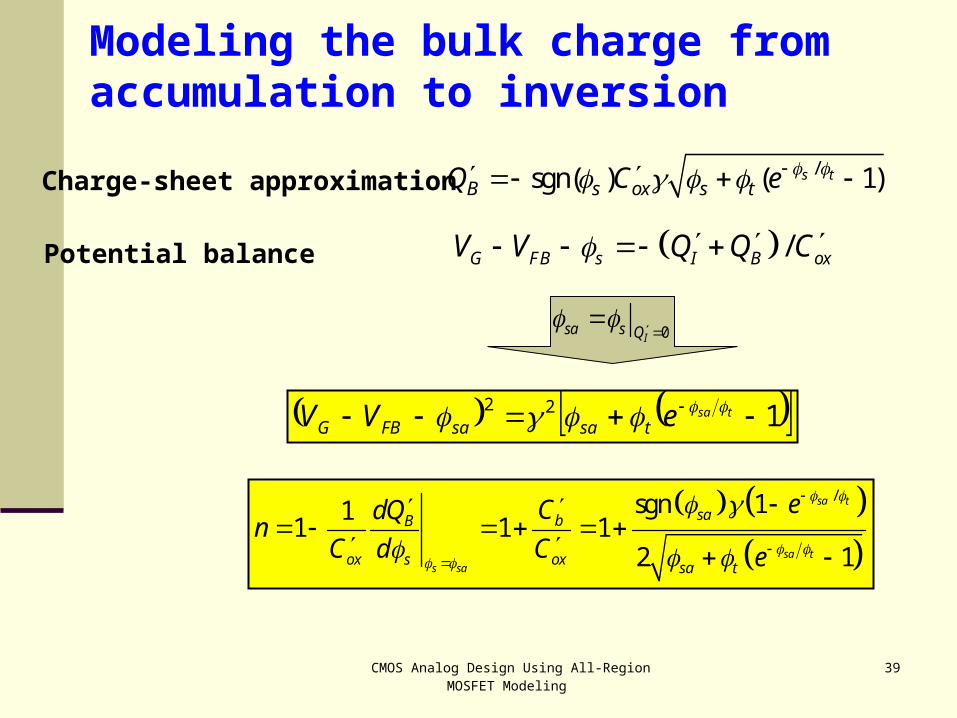
Modeling the bulk charge from accumulation to inversion
/sgn( ) ( 1)s tB s ox s tQ C e
/sgn 111 1 1
2 1
sa t
sa ts sa
sabB
ox s ox sa t
eCdQn
C d C e
/G FB s I B oxV V Q Q C
Charge-sheet approximation
122 tsaeVV tsasaFBG
0Isa s Q
Potential balance

CMOS Analog Design Using All-Region MOSFET Modeling
40
Modeling from accumulation to inversion: Surface potential and pinch-off voltage (VP)

CMOS Analog Design Using All-Region MOSFET Modeling
41
Transistor symmetry
, ,D D G S DI I V V V
Voltages referenced to local substrate:
VG VGB VS VSB VD VDB
VG
VDVS
B ID
1.
2. Symmetry
1 2 2 1, , , ,D G D GI V V V I V V V
VG
V2V1
B
ID
CMOS Analog Design Using All-Region MOSFET Modeling
42
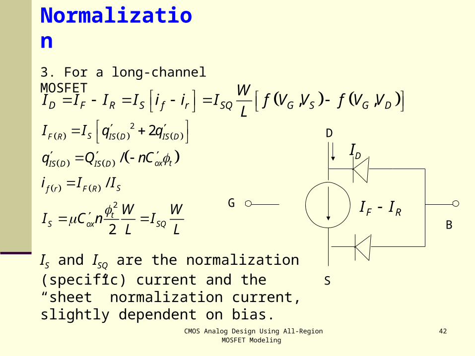
, ,D F R S f r SQ G S G DW
I I I I i i I f V V f V VL
2
2
2
/
/
2
SF R IS D IS D
ox tIS D IS D
Sf r F R
tS ox SQ
I I q q
q Q nC
i I I
W WI C n I
L L
3. For a long-channel MOSFET
IS and ISQ are the normalization (specific) current and the “sheet” normalization current, slightly dependent on bias.
Normalization
D
S
B
ID
F RI IG
CMOS Analog Design Using All-Region MOSFET Modeling
43
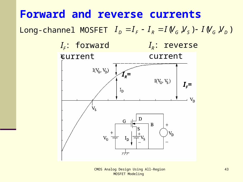
Long-channel MOSFET ),(),( DGSGRFD VVIVVIIII
IF: forward current IR: reverse current
IF=
IR=
Forward and reverse currents

CMOS Analog Design Using All-Region MOSFET Modeling
44
The specific (normalization) current2
2t
S ox SQ
W WI C n I
L L
ISQ : process parameter slightly dependent on VG and T
ISQ 25 nA (p-channel)
ISQ 75 nA (n-channel)
in 0.35 m CMOS
Specific current

CMOS Analog Design Using All-Region MOSFET Modeling
45
22
0 2 22 2P G T F FV V V
( ) ( ) ( )1 lnP S D t IS D IS DV V q q ( ) ( )1 1IS D f rq i UCCM &
VT0
VP
VG
Slope =1 Slope =1/n
VG0
VP0
Linearization:
0
00
G GP P
G
V VV V
n V
0
0
12 2
G
P F
n VV
In particular:
0
0
G TP
T
V VV
n V
0 12 2
T
F
n V
Pinch-off voltage and slope factor (1)

CMOS Analog Design Using All-Region MOSFET Modeling
46
Determination of the pinch-off voltage and the slope factor as functions of VG. NMOS transistor W=20 m, L=2 m, 0.18 m CMOS technology.
Pinch-off voltage and slope factor (2)

CMOS Analog Design Using All-Region MOSFET Modeling
47
Common-source characteristics
1,00E-09
1,00E-08
1,00E-07
1,00E-06
1,00E-05
1,00E-04
1,00E-03
0,00E+00 5,00E-01 1,00E+00 1,50E+00 2,00E+00 2,50E+00 3,00E+00 3,50E+00 4,00E+00 4,50E+00
10-3
10-6
10-9
VS = 0 V
3.0
2.5
2.01.5
0.5 1.0
0 1 2 3 4 VG (V)
ID (A) VD = VG
1 2 ln 1 1P S t f fV V i i
VD
ID
VGVS
The I-V relationship (1)

CMOS Analog Design Using All-Region MOSFET Modeling
48
VG = 4.8 V
ID (A) VD = VG
10-3
10-6
10-9
0 1 2 3 VS (V)
0.8 V
Common-gate characteristics VG=0.8, 1.2, 1.6, 2.0, 2.4, 3.0, 3.6, 4.2, and 4.8 V
VD
ID
VS
VG
( )1 2 ln 1 1P S t f f rV V i i
The I-V relationship (2)

CMOS Analog Design Using All-Region MOSFET Modeling
49
0( ) ( ) ( )1 2 ln 1 1G T
S D t f r f r
V VV i i
n
Weak inversion
if(r)<1
-1 if(r)/20 /
/0 1
G TS t
DS t
V VV
VnDI I e e
2 11
0 2ox Sn t
WI nC I ee
L
Weak inversion model

CMOS Analog Design Using All-Region MOSFET Modeling
50
0( ) ( ) ( )1 2 ln 1 1G T
S D t f r f r
V VV i i
n
Strong inversion
if(r)>>10
( ) ( ) ( )G T
S D t f r t F R S
V VV i I I
n
2 20 02D F R ox G T S G T Dn
WI I I C V V nV V V nV
nL
Moderate inversion 1<if(r) <100 Both sqrt(.) and ln(.) terms are important
Strong inversion model (1)
CMOS Analog Design Using All-Region MOSFET Modeling
51
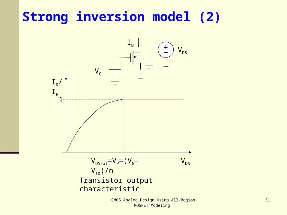
ID/IF
1
VDSsat=VP=(VG-VT0)/n VDS
VDS
ID
VG
Transistor output characteristic
Strong inversion model (2)
CMOS Analog Design Using All-Region MOSFET Modeling
52
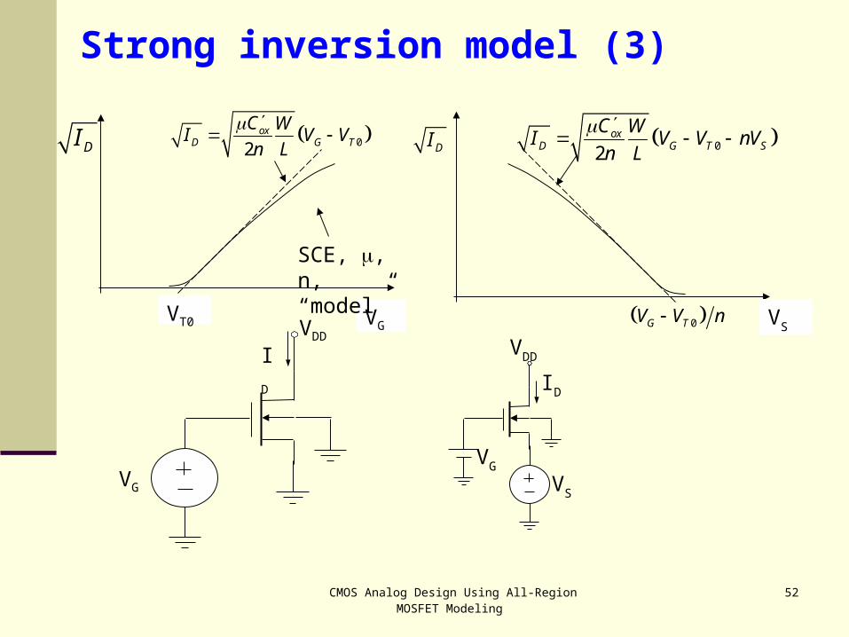
VDD
ID
VG
VGVT0
DI 02ox
D G T
C WI V V
n L
SCE, , n, “model”
0G TV V n
02ox
D G T S
C WI V V nV
n L
DI
VS
VDD
ID
VS
VG
Strong inversion model (3)

CMOS Analog Design Using All-Region MOSFET Modeling
53
1 1ln 1 1 ln
1 1
fDS ISIS ID f r
t ID r
iV qq q i i
q i
(a) if= 4.5x 10⁻² (VG=0.7 V); (b) if= 65(VG= 1.2 V); (c) if= 9.5x10² (VG= 2.0 V); (d) if= 3.1x 10³ (VG= 2.8 V); (e) if= 6.8x 10³ (VG= 3.6 V); (f) if= 1.2x 10⁴ (VG= 4.4 V).
Universal output characteristics
(o): measured (—): model
CMOS Analog Design Using All-Region MOSFET Modeling
54
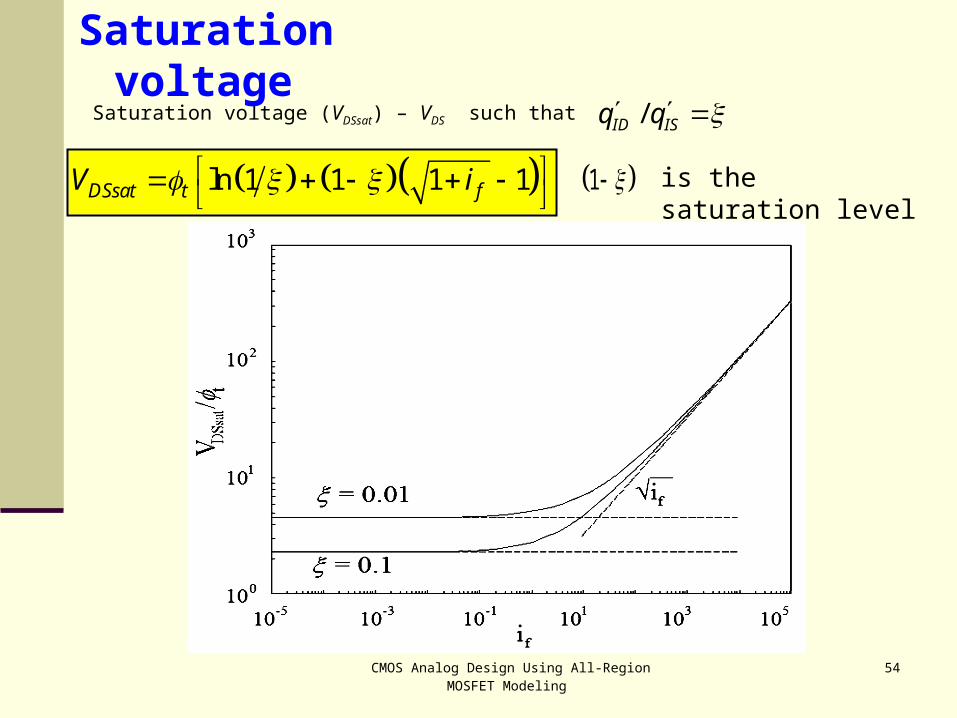
Saturation voltage (VDSsat) – VDS such that /ID ISq q
ln 1 1 1 1DSsat t fV i 1 is the saturation level
Saturation voltage
CMOS Analog Design Using All-Region MOSFET Modeling
55
r r
G D
i i
V n V
F R Fms IS
S S
I I I Wg Q
V V L
BmbDmdSmsGmgD VgVgVgVgI
B
Dmb
D
Dmd
S
Dms
G
Dmg V
Ig
V
Ig
V
Ig
V
Ig
,,,
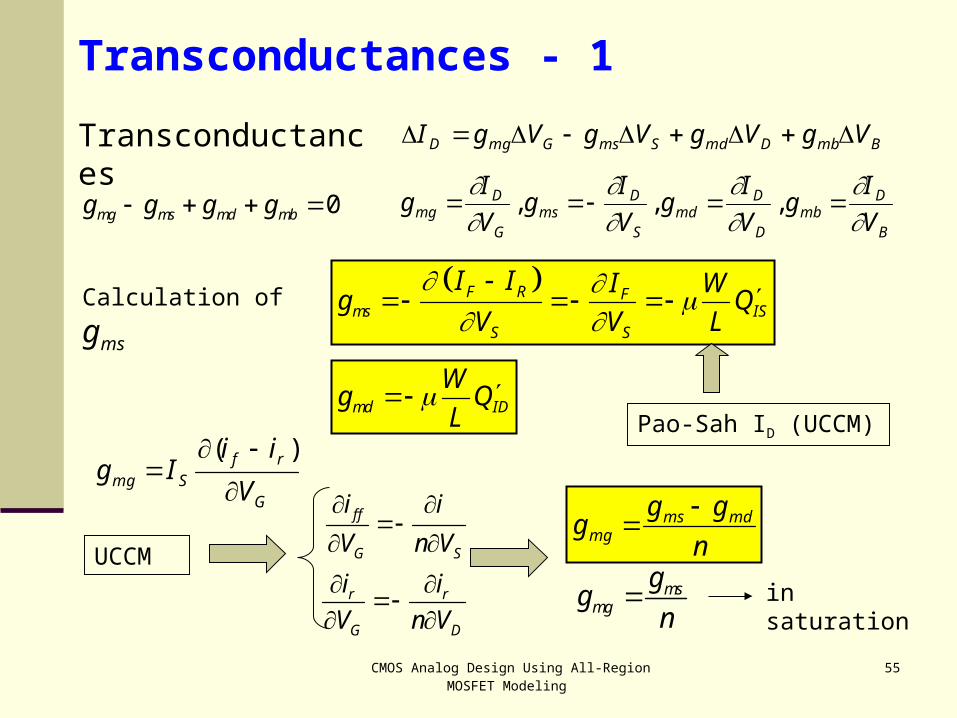
Transconductances
Calculation of gms
Pao-Sah ID (UCCM)md ID
Wg Q
L
G
rfSmg V
iiIg
)(
UCCM
f f
G S
i i
V n V
n
ggg mdms
mg
msmg
gg
n in saturation
Transconductances - 1
0mg ms md mbg g g g

CMOS Analog Design Using All-Region MOSFET Modeling
56
Source transconductance VG= 0.8, 1.2, 1.6, 2.0, 2.4, 3.0, 3.6, 4.2, and 4.8 V (W=L=25 m, tox=280 Å)
VDD
ID
VS
VG
Transconductances - 2

CMOS Analog Design Using All-Region MOSFET Modeling
57
Gate transconductance VS= 0, 0.5, 1.0,1.5, 2.0, 2.5, and 3.0 V . W=L=25 m, tox=280 Å
VDD
ID
VGVS
Transconductances - 3
CMOS Analog Design Using All-Region MOSFET Modeling
58
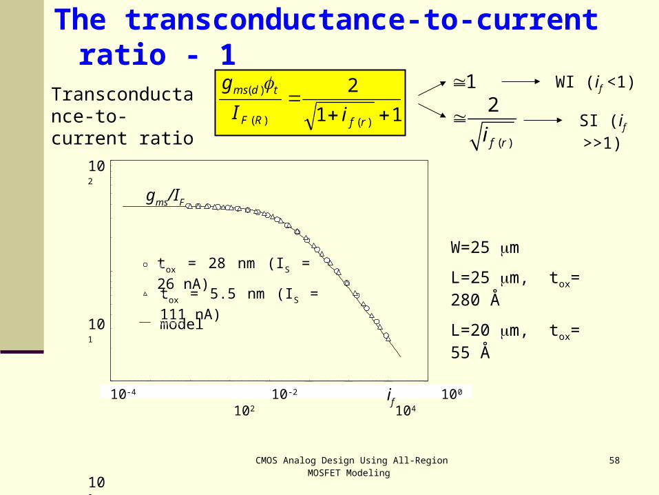
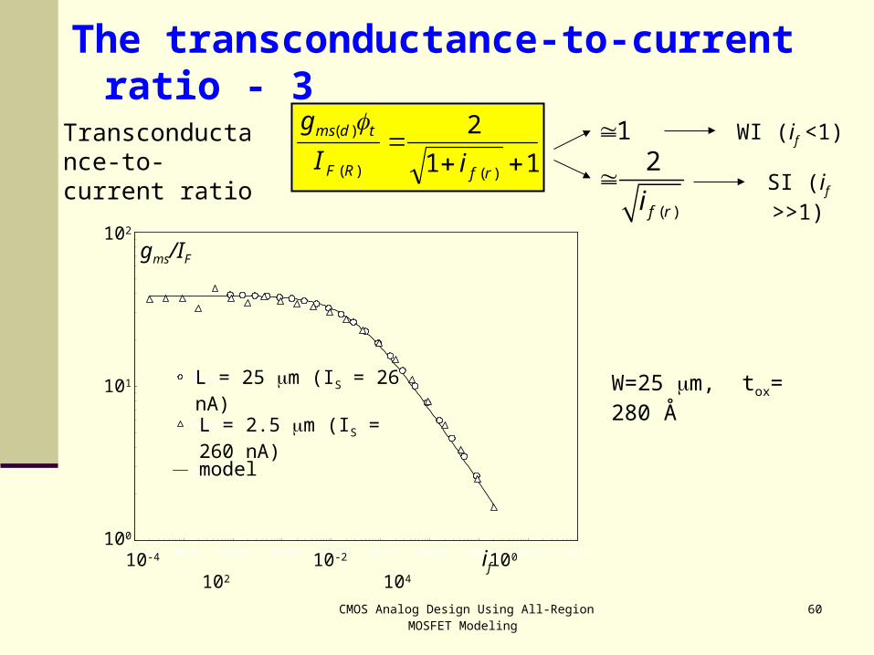
Transconductance-to-current ratio 11
2
)()(
)(
rfRF
tdms
iI
g 1
( )
2
f ri
WI (if <1)
SI (if >>1)
W=25 m
L=25 m, tox= 280 Å
L=20 m, tox= 55 Å
The transconductance-to-current ratio - 1
10-4 10-2 100 102 104if
tox = 28 nm (IS = 26 nA)
model
102
101
100
gms/IF
tox = 5.5 nm (IS = 111 nA)
1,00E-03 1,00E-01
Seqüência1
Seqüência2
Seqüência3

CMOS Analog Design Using All-Region MOSFET Modeling
59
Transconductance-to-current ratio 11
2
)()(
)(
rfRF
tdms
iI
g 1
( )
2
f ri
WI (if <1)
SI (if >>1)
W=L=25 m, tox= 280 Å
1,00E+00
1,00E+01
1,00E+02
1,00E-04 1,00E-03 1,00E-02 1,00E-01 1,00E+00 1,00E+01 1,00E+02 1,00E+03 1,00E+04
Seqüência1
Seqüência2
Seqüência3
Seqüência4
10-4 10-2 100 102 104
VGB = 2.0 V (IS = 26 nA)
VGB = 1.0 V (IS = 33 nA)
VGB = 3.0 V (IS = 24 nA)
model
if
102
101
100
gms/IF
The transconductance-to-current ratio - 2
CMOS Analog Design Using All-Region MOSFET Modeling
60
Transconductance-to-current ratio 11
2
)()(
)(
rfRF
tdms
iI
g 1
( )
2
f ri
WI (if <1)
SI (if >>1)
W=25 m, tox= 280 Å
1
10
100
1,00E-04 1,00E-03 1,00E-02 1,00E-01 1,00E+00 1,00E+01 1,00E+02 1,00E+03 1,00E+04 1,00E+05
Seqüência1
Seqüência2
Seqüência3
L = 25 m (IS = 26 nA)
model
10-4 10-2 100 102 104if
102
101
100
gms/IF
L = 2.5 m (IS = 260 nA)
The transconductance-to-current ratio - 3

CMOS Analog Design Using All-Region MOSFET Modeling
61
G
B
S D
id
dmd vg
bmbvg
smsvg
gmgvg
The low-frequency small-signal model
CMOS Analog Design Using All-Region MOSFET Modeling
62
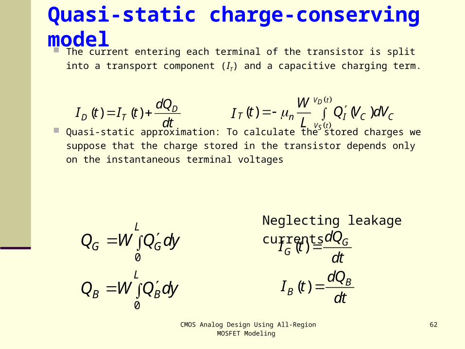
Quasi-static charge-conserving model The current entering each terminal of the transistor is split into a transport
component (IT) and a capacitive charging term.
Quasi-static approximation: To calculate the stored charges we suppose
that the charge stored in the transistor depends only on the instantaneous
terminal voltages
( ) ( ) DD T
dQI t I t
dt
0
0
L
G G
L
B B
Q W Q dy
Q W Q dy
( ) GG
dQI t
dt
( ) BB
dQI t
dt
( ) ( )
V tD
V tS
T n I C CW
t Q V dVIL
Neglecting leakage currents

CMOS Analog Design Using All-Region MOSFET Modeling
63
Ward-Dutton partition of the channel charge
As expected
is the total inversion charge stored
in the channel0
L
I IQ W Q dy
0
L
D Iy
Q W Q dyL
( ) ( ) SD ID S
dQdQ dQI t I t
dt dt dt
0(1 )
L
S Iy
Q W Q dyL
( ) ( ) SS T
dQI t I t
dt ( ) ( ) D
D TdQ
I t I tdt

CMOS Analog Design Using All-Region MOSFET Modeling
64
Calculation of stored charge - 1
It is convenient to define
D drift diff
s II tn n
I I I
d dQWQ W
dy dy
I ox sdQ nC d '
nI ox t I
ox D
Wdy Q nC dQ
nC I
It I ox tQ Q nC
'n
It Itox D
Wdy Q dQ
nC I

CMOS Analog Design Using All-Region MOSFET Modeling
65
'n
It Itox D
Wdy Q dQ
nC I
2F
R
Qn
I It ox t It ItQD ox
WQ Q nC Q dQ
I nC
0
L
I IQ W Q dy
2 3 3 2 2
3 2n R F R F
I ox tox D
W Q Q Q QQ nC
nC I
2 22
3F F R R
ox tIF R
Q Q Q QWL nCQ
Q Q
2 22 3( ) ( )
2IS IS ID ID ox t IS ID
IIS ID ox t
Q Q Q Q nC Q QQ WL
Q Q nC
2 3I ISQ WLQ
( )
2IS ID
IQ Q
Q WL
In weak inversion
In strong inversion & saturation
or
( ) ( )F R IS D ox tQ Q nC
Using we find that
Calculation of stored charge - 2
2 2
2
( / )
2n t
D F R
ox t
W LI Q Q
nC

CMOS Analog Design Using All-Region MOSFET Modeling
66
Total inversion, source and drain charges
Channel linearity coefficient
ID ox tR
F IS ox t
Q nCQ
Q Q nC
=1 in WI
=1 in SI for VDS=0
0 in SI sat
22 1( )
3 1I IS ox t ox tQ WL Q nC nC
2 3
2
6 12 8 4( )
215 1S IS ox t ox t
nQ WL Q nC C
2 3
2
4 8 12 6( )
215 1D IS ox t ox t
nQ WL Q nC C
CMOS Analog Design Using All-Region MOSFET Modeling
67
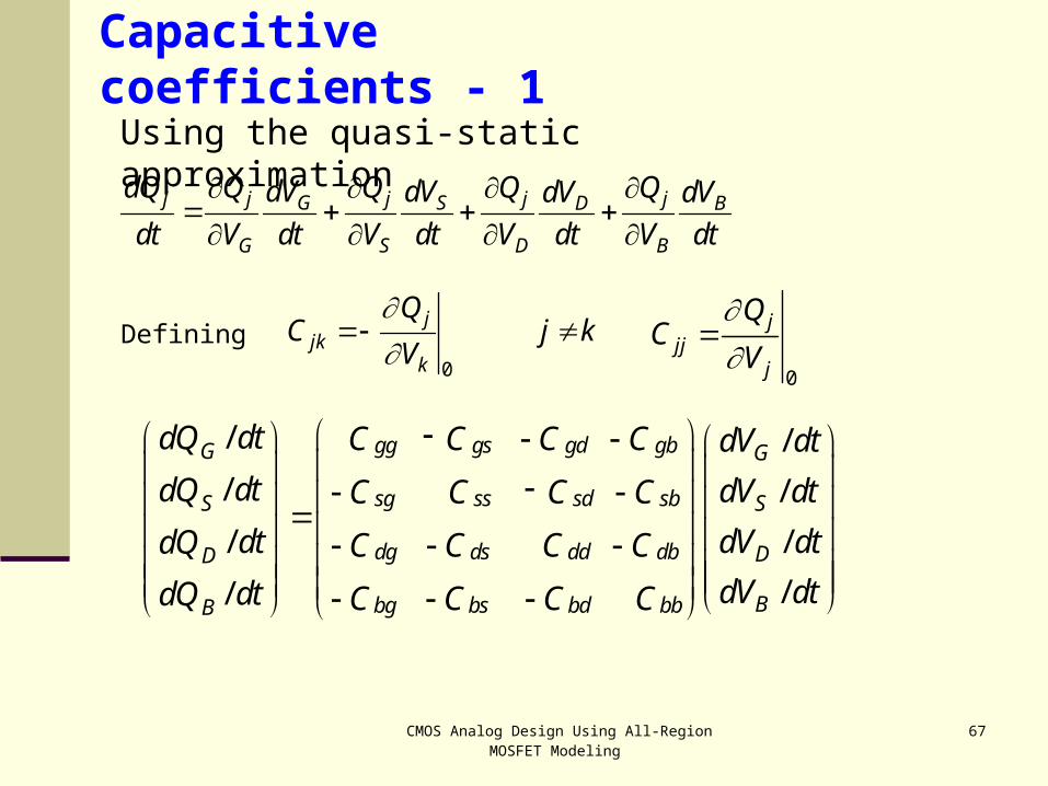
Capacitive coefficients - 1
j j j j jG S D B
G S D B
dQ Q Q Q QdV dV dV dV
dt V dt V dt V dt V dt
0
jjk
k
QC j k
V
0
jjj
j
QC
V
/ /
/ /
/ /
//
gg gs gd gbG G
sg ss sd sbS S
dg ds dd db DD
Bbg bs bd bbB
dtdQ C C C C dV dt
dtdQ dV dtC C C C
dt dV dtdQ C C C C
dV dtdtdQ C C C C
Using the quasi-static approximation
Defining
CMOS Analog Design Using All-Region MOSFET Modeling
68
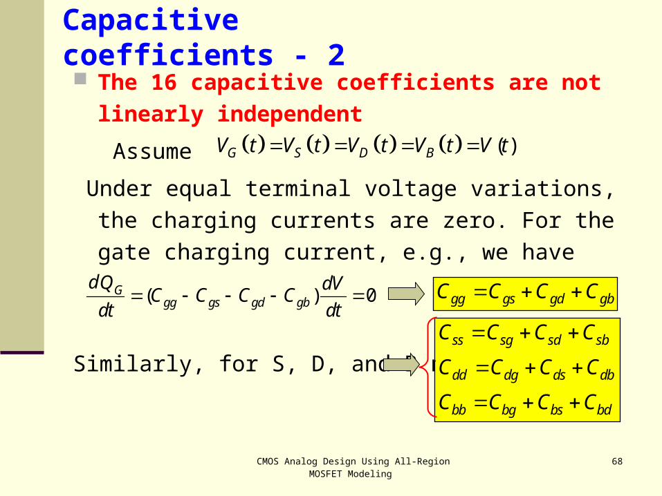
The 16 capacitive coefficients are not linearly
independent
Assume
Under equal terminal voltage variations, the charging
currents are zero. For the gate charging current, e.g.,
we have
Similarly, for S, D, and B nodes
( )G S D BV t V t V t V t V t
( ) 0Ggg gs gd gb
dQ dVC C C C
dt dt gg gs gd gbC C C C
ss sg sd sb
dd dg ds db
bb bg bs bd
C C C C
C C C C
C C C C
Capacitive coefficients - 2
CMOS Analog Design Using All-Region MOSFET Modeling
69
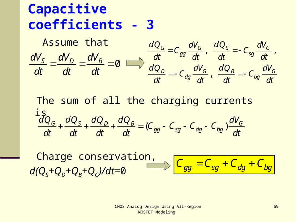
Assume that
The sum of all the charging currents is
Charge conservation,
d(QS+QD+QB+QG)/dt=0
0S D BdV dV dV
dt dt dt
, ,
,
G G S Ggg sg
G GD Bdg bg
d dQ QdV dVC C
dt dt dt dtd dQ QdV dV
C Cdt dt dt dt
( )G S GD Bgg sg dg bg
d d d dQ Q Q Q dVC C C C
dt dt dt dt dt
gg sg dg bgC C C C
Capacitive coefficients - 3

CMOS Analog Design Using All-Region MOSFET Modeling
70
Linear relationships between capacitive coefficients
Only nine out of the sixteen capacitive coefficients are linearly independent
gg gs gd gb sg dg bg
ss sg sd sb gs ds bs
dd dg ds db gd sd bd
bb bg bs bd gb sb db
C C C C C C C
C C C C C C C
C C C C C C C
C C C C C C C
Capacitive coefficients - 4
CMOS Analog Design Using All-Region MOSFET Modeling
71
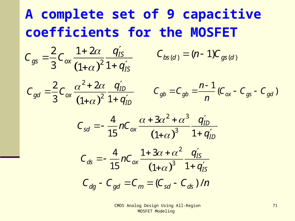
A complete set of 9 capacitive coefficients for the MOSFET
2
2 1 2
3 11IS
gs oxIS
qC C
q
2
2
2 2
3 11ID
gd oxID
qC C
q
( ) ( )( 1)bs d gs dC n C
1( )gb gb ox gs gd
nC C C C C
n
2 3
3
4 3
15 11ID
sd oxID
qC nC
q
2
3
4 1 3
15 11IS
ds oxIS
qC nC
q
( ) / dg gd m sd dsC C C C C n
CMOS Analog Design Using All-Region MOSFET Modeling
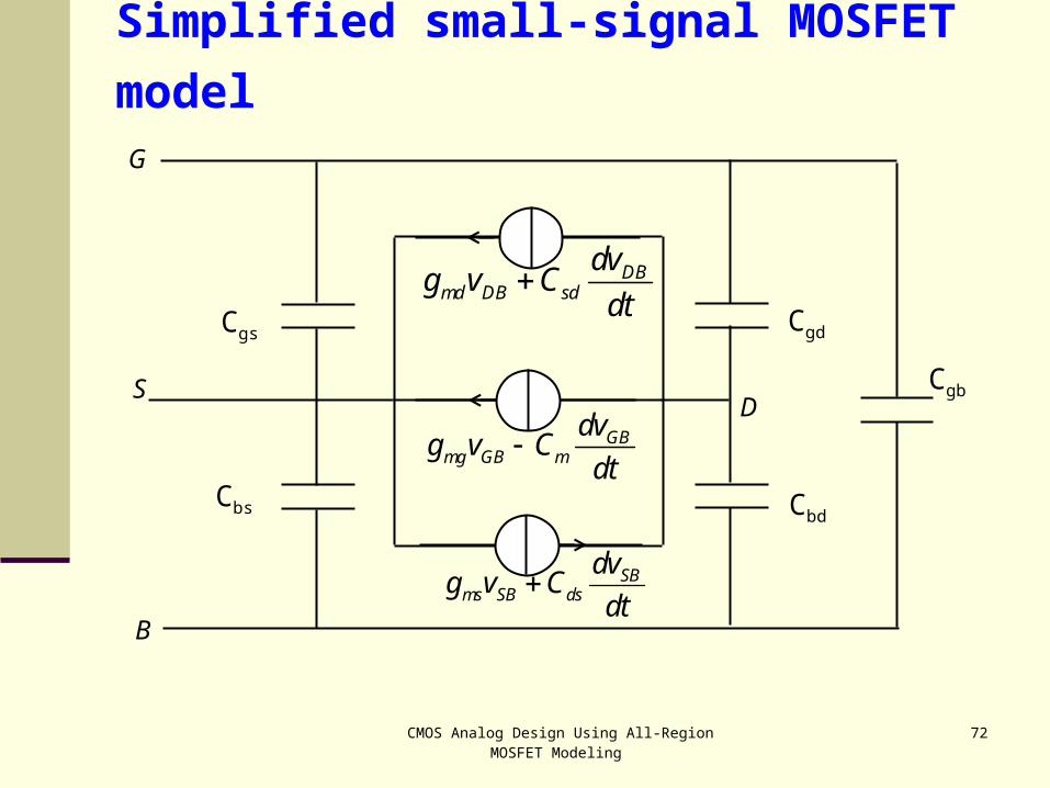
72
Simplified small-signal MOSFET model
G
DS
B
DBmd DB sd
dvg v C
dt
GBmg GB m
dvg v C
dt
SBms SB ds
dvg v C
dt
Cgs
Cbs
Cgd
Cbd
Cgb

CMOS Analog Design Using All-Region MOSFET Modeling
73
The five capacitances of the simplified model
Intrinsic capacitances simulated from (___) the charge-based and (o) from the S- model (NMOS transistor, tox= 250Å, NA=2x1016 cm-3, and VT0=0.7V.
CMOS Analog Design Using All-Region MOSFET Modeling
74
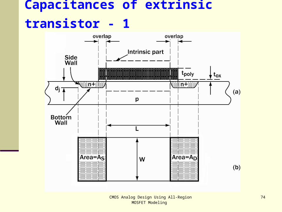
Capacitances of extrinsic transistor - 1
CMOS Analog Design Using All-Region MOSFET Modeling
75
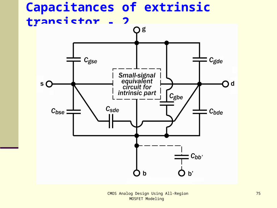
Capacitances of extrinsic transistor - 2

CMOS Analog Design Using All-Region MOSFET Modeling
76
Non-quasi-static (NQS) small-signal
model Channel segmentation: representation of the MOSFET
as a series combination of short transistors

CMOS Analog Design Using All-Region MOSFET Modeling
77
Simplified high-frequency MOSFET model
1 21gsC
j
1 21bsC
j
11md dg v
j
11mg gg v
j
11ms sg v
j
1 31gdC
j
1 41gb
gb
CC
j
1 31bdC
j
G
DS
B

CMOS Analog Design Using All-Region MOSFET Modeling
78
Time constants of the NQS MOSFET model
2
1 3
4 1 3
1 15 1ISq
2
2 2
1 2 8 5
1 15 (1 ) (1 2 )ISq
2
3 2
1 5 8 2
1 15 (1 (2 ))ISq
2
t
L

CMOS Analog Design Using All-Region MOSFET Modeling
79
Quasi-static small-signal model
1<<1 2(3)<<1 non-quasi-static model reduces to the five-capacitor model
B
G
DS
md DBg v
mg GBg v
ms SBg v
gsC
bsC
gdC
bdC
gbC
CMOS Analog Design Using All-Region MOSFET Modeling
80
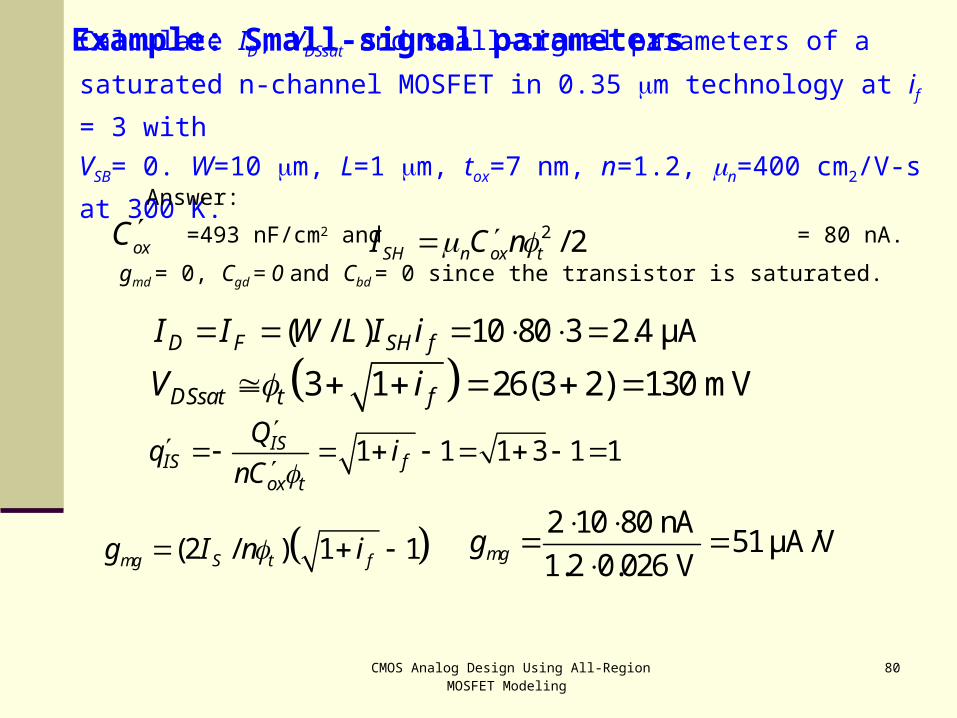
Calculate ID, VDSsat and small-signal parameters of a saturated n-
channel MOSFET in 0.35 m technology at if = 3 with
VSB= 0. W=10 m, L=1 m, tox=7 nm, n=1.2, n=400 cm2/V-s at 300 K. Answer:
=493 nF/cm2 and = 80 nA.
gmd = 0, Cgd = 0 and Cbd = 0 since the transistor is saturated.
oxC 2 / 2SH n ox tI C n
( / ) 10 80 3 2.4 μAD F SH fI I W L I i
3 1 26(3 2) 130 mVDSsat t fV i
(2 / ) 1 1mg S t fg I n i
1 1 1 3 1 1ISIS f
ox t
Qq i
nC
2 10 80 nA51 μA/V
1.2 0.026 Vmgg
Example: Small-signal parameters

CMOS Analog Design Using All-Region MOSFET Modeling
81
=1/(1+1)=0.5
2
2 1 2
3 11IS
gs oxIS
qC C
q
1
( )gb ox gs gdn
C C C Cn
49 fFox oxC WLC
1 1
1 1ID
IS IS
q
q q
22 1 1 1
49 14.5 fF3 1 11 0.5
gsC
0.2(49 14.5 0) 5.75 fF
1.2gbC
Example: Small-signal parameters (continued)

CMOS Analog Design Using All-Region MOSFET Modeling
82
Intrinsic transition frequency
2 2mg ms
Tgs gb gs gb
g gf
C C n C C
22 1 1
2t
T ff iL
CMOS Analog Design Using All-Region MOSFET Modeling
83
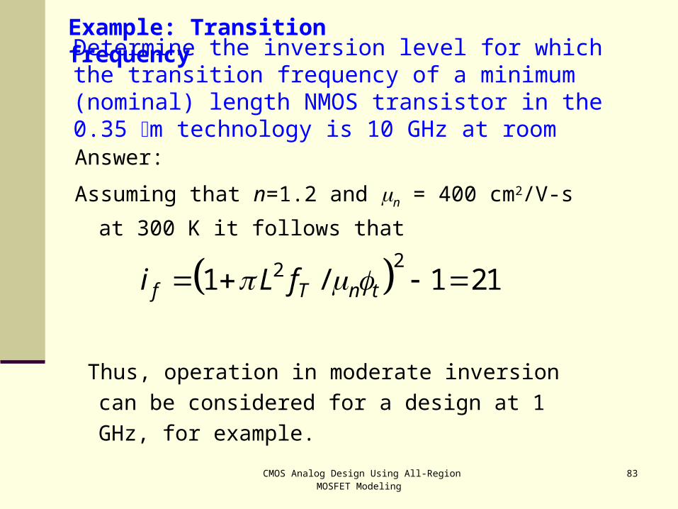
Determine the inversion level for which the transition frequency of a minimum (nominal) length NMOS transistor in the 0.35 m technology is 10 GHz at room
Answer:
Assuming that n=1.2 and n = 400 cm2/V-s at 300 K it
follows that
Thus, operation in moderate inversion can be
considered for a design at 1 GHz, for example.
221 / 1 21f T n ti L f
Example: Transition frequency
CMOS Analog Design Using All-Region MOSFET Modeling
84
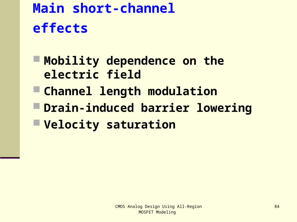
Main short-channel effects
Mobility dependence on the electric field Channel length modulation Drain-induced barrier lowering Velocity saturation
CMOS Analog Design Using All-Region MOSFET Modeling
85
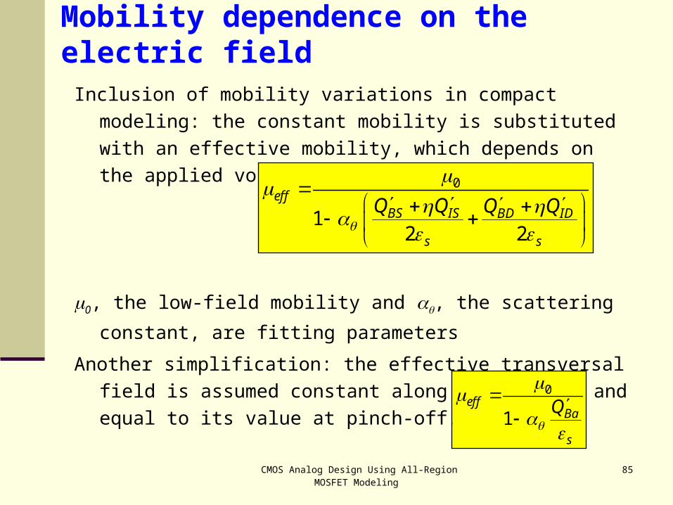
Mobility dependence on the electric field
Inclusion of mobility variations in compact modeling: the constant
mobility is substituted with an effective mobility, which depends
on the applied voltages.
0, the low-field mobility and , the scattering constant, are fitting
parameters
Another simplification: the effective transversal field is assumed
constant along the channel and equal to its value at pinch-off.
0
12 2
effBS IS BD ID
s s
Q Q Q Q
0
1eff
Ba
s
Q
CMOS Analog Design Using All-Region MOSFET Modeling
86
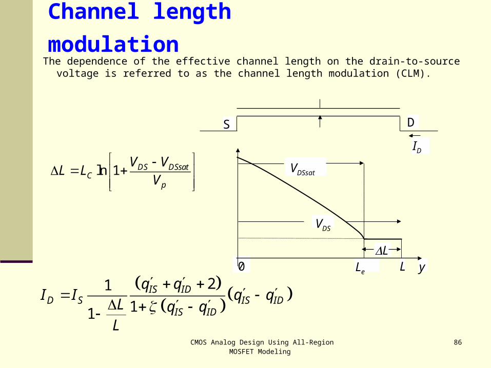
Channel length modulation The dependence of the effective channel length on the drain-to-source
voltage is referred to as the channel length modulation (CLM).
ln 1 DS DSsatC
p
V VL L
V
21
11
IS IDD S IS ID
IS ID
q qI I q q
L q qL
y
S
0
ID
VDSsat
Le L
VDS
L
D

CMOS Analog Design Using All-Region MOSFET Modeling
87
Drain-induced barrier lowering (DIBL) An increase in the drain voltage produces an increase in the
surface potential in the channel and, consequently, a reduction in the potential barrier seen by the electrons at the source ( DIBL).
The inclusion of the DIBL effect in MOSFET models is generally through the threshold voltage.
11, 4
exp26
d
LVV
d
tVV DSBSbi
oxlcTT
,T DBSBT lc bi biV V V V
CMOS Analog Design Using All-Region MOSFET Modeling
88
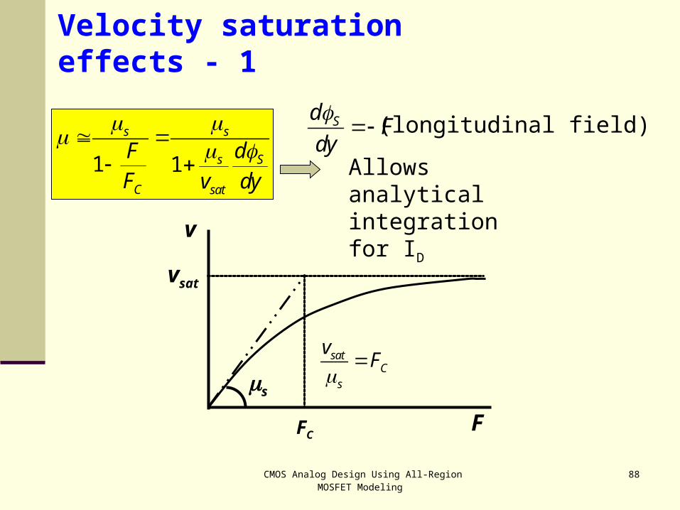
1 1
s s
s S
C sat
F dF v dy
satC
s
vF
SdF
dy
(longitudinal field)
vsat
v
F
s
FC
Velocity saturation effects - 1
Allows analytical integration for ID
CMOS Analog Design Using All-Region MOSFET Modeling
89
1
s
s I
ox sat
dQ
nC v dy
Velocity saturation effects - 2
I ox sdQ nC d
CD I
dVI WQ
dy 1 t CI
ox I
dVdQ
dy nC Q dy
11
1
s I tID
I ox I
ox C
WQ dQI
dQ dy nC QnC F dy
1
21
ID ISsD IP ID IS
ID ISox
C ox
Q QWI Q Q Q
Q QnC LLF nC
CMOS Analog Design Using All-Region MOSFET Modeling
90
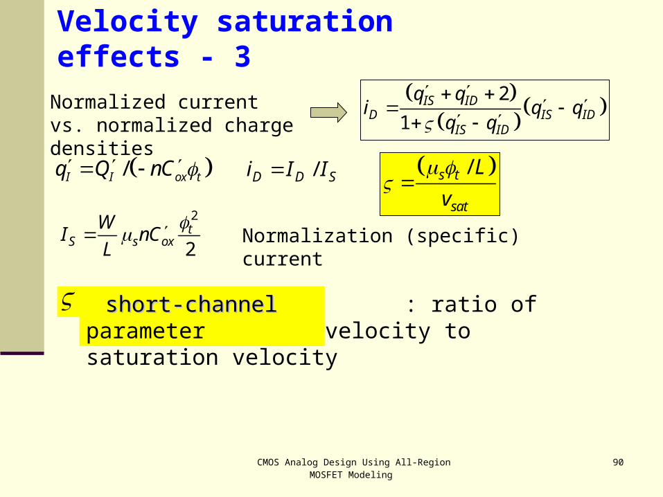
Velocity saturation effects - 3
2
2t
S s oxW
I nCL
2
1IS ID
D IS IDIS ID
q qi q q
q q
/I I ox tq Q nC
Normalized current vs. normalized charge densities
/D D Si I I
Normalization (specific) current
: ratio of diffusion-related velocity to saturation velocity
/s t
sat
L
v
short-channel short-channel parameter
CMOS Analog Design Using All-Region MOSFET Modeling
91
0
SD
ID
VDS
IDQ
IDSATQ
ISQ IQ
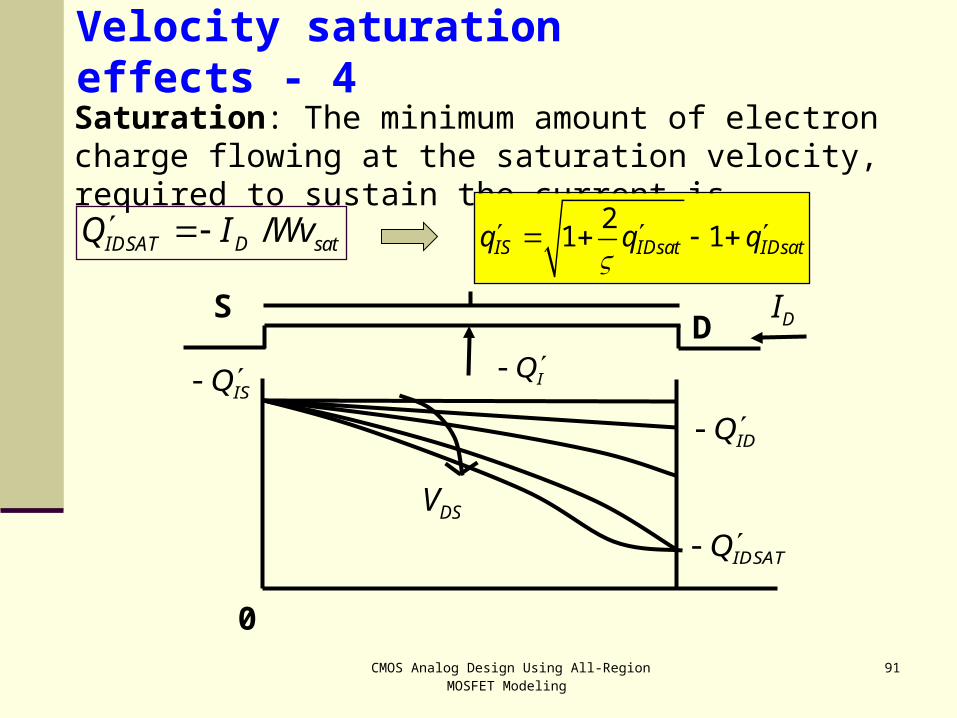
Saturation: The minimum amount of electron charge flowing at the saturation velocity, required to sustain the current is
/IDSAT D satQ I Wv
Velocity saturation effects - 4
21 1IS IDsat IDsatq q q

CMOS Analog Design Using All-Region MOSFET Modeling
92
Velocity saturation effects - 5
21 1IS IDsat IDsatq q q
10-2 100 102 104
1
weak inversion
strong inversion
toxIS CnQ
ISIDSAT QQ
s t
sat
L
v
Short channel
Long channel
CMOS Analog Design Using All-Region MOSFET Modeling
93
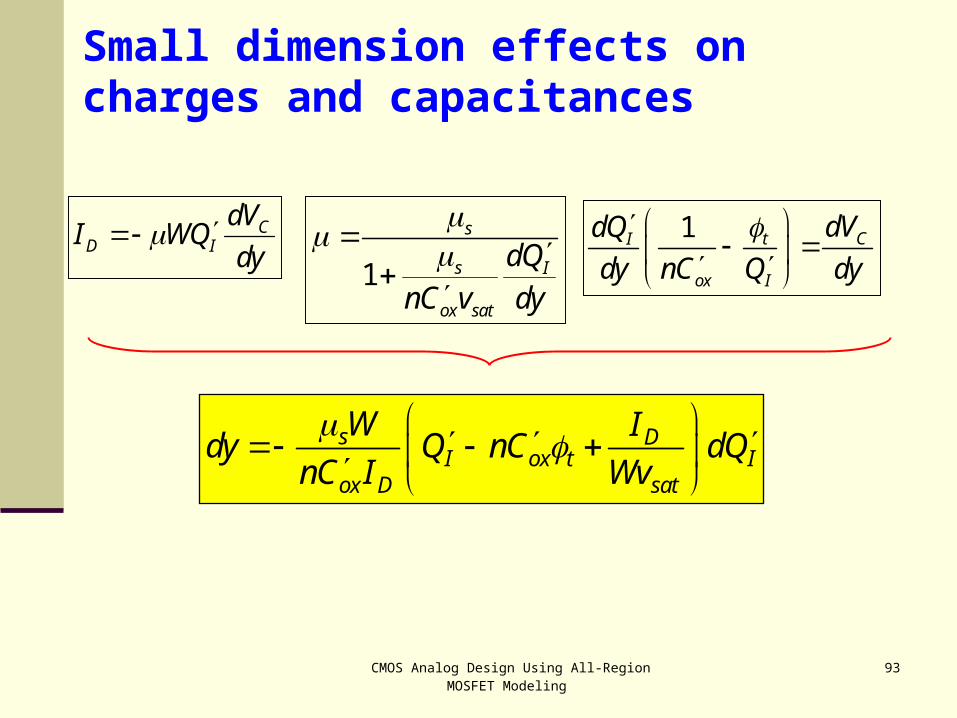
Small dimension effects on charges and capacitances
s DI ox t I
ox D sat
W Idy Q nC dQ
nC I Wv
1
s
s I
ox sat
dQ
nC v dy
CD I
dVI WQ
dy 1 t CI
ox I
dVdQ
dy nC Q dy

CMOS Analog Design Using All-Region MOSFET Modeling
94
Virtual inversion charge density
inversion +pinch off -saturation charge densities
Along the channel
DV I ox t
sat
IQ Q nC
Wv
V IdQ dQ
s sDI ox t I V V
ox D sat ox D
W WIdy Q nC dQ Q dQ
nC I Wv nC I
Virtual charge formalism - 1
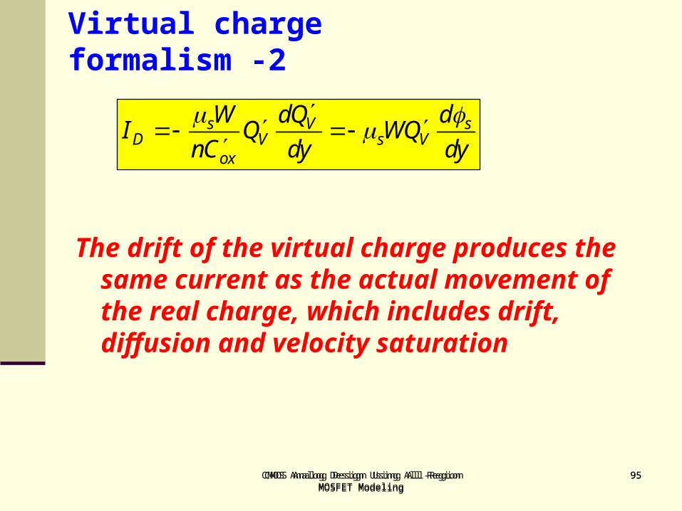
CMOS Analog Design Using All-Region MOSFET Modeling
95CMOS Analog Design Using All Region MOSFET Modeling
95
The drift of the virtual charge produces the same current as the actual movement of the real charge, which includes drift, diffusion and velocity saturation
s V sD V s V
ox
W dQ dI Q WQ
nC dy dy
Virtual charge formalism -2
CMOS Analog Design Using All-Region MOSFET Modeling
96
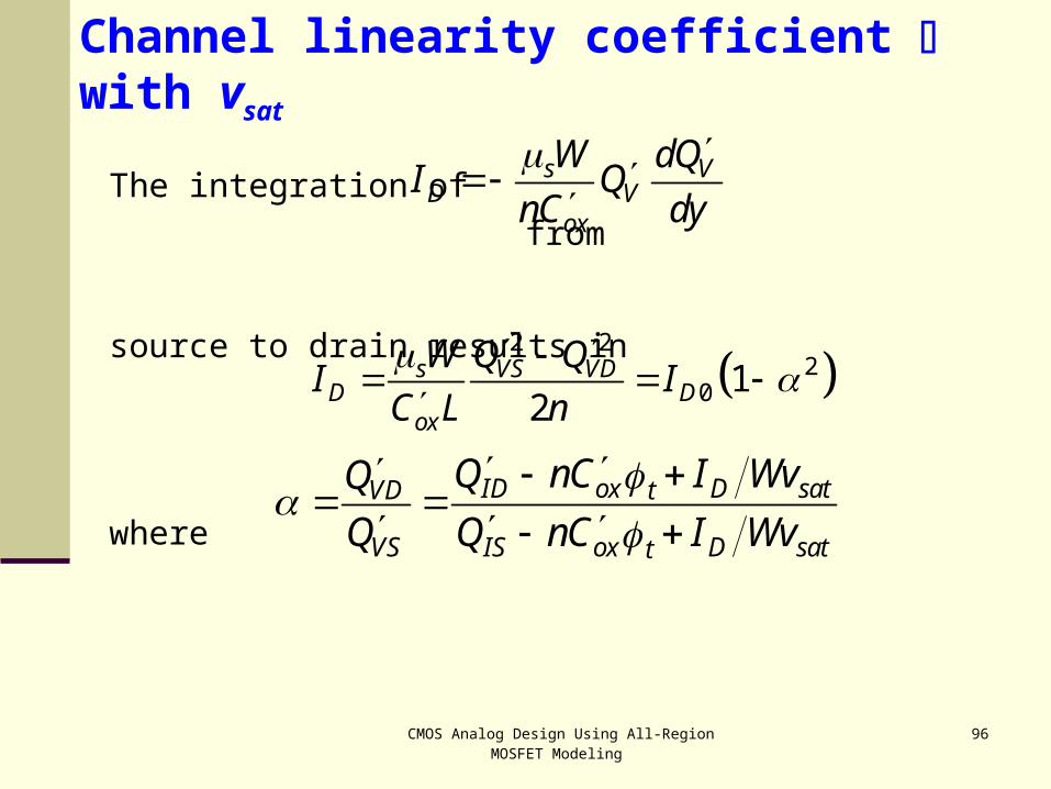
Channel linearity coefficient with vsat
The integration of from
source to drain results in
where
s VD V
ox
W dQI Q
nC dy
2 2
20 1
2s VS VD
D Dox
W Q QI I
C L n
ID ox D satVD t
VS IS ox D satt
Q nC I WvQ
Q Q nC I Wv

CMOS Analog Design Using All-Region MOSFET Modeling
97
Stored charges including vsat
The stored charge
is calculated changing the integration variable
from y to
resulting in
0L L
I I IDsatQ W Q dy W LQ
sV V
ox D
Wdy Q dQ
nC I
22 1( )
3 1D
VS ox tIsat
LIW L L Q nCQ
v
VQ

CMOS Analog Design Using All-Region MOSFET Modeling
98
Source and drain charges including vsat

CMOS Analog Design Using All-Region MOSFET Modeling
99
Capacitive coefficients including vsat - 1
2
2 2
12 1 2
3 1 3(1 ) 1IS e ms
gs e oxIS sat
q L gC WL C
q nv
22
2 2
12 2
3 1 3(1 ) 1e mdID
gd e oxID sat
L gqC WL C
q nv
( ) ( )1bs d gs dC n C
2
2
11
3 1
e mggb bg ox gso gdo
sat
L gnC C C C C
n v
22 22
3 3
3 7 14 1 3 1
15 1 301 1
ee IS msds ox
IS sat
gq LLC nC WL q v L
22 3 22
3 3
3 7 14 3 1
15 1 301 1
ee mdIDsd ox
ID sat
gq LLC nC WL q v L
/dg gd sd dsC C C C n

CMOS Analog Design Using All-Region MOSFET Modeling
100
Normalized capacitances versus drain-source voltage
Capacitive coefficients including vsat - 1
CMOS Analog Design Using All-Region MOSFET Modeling
101
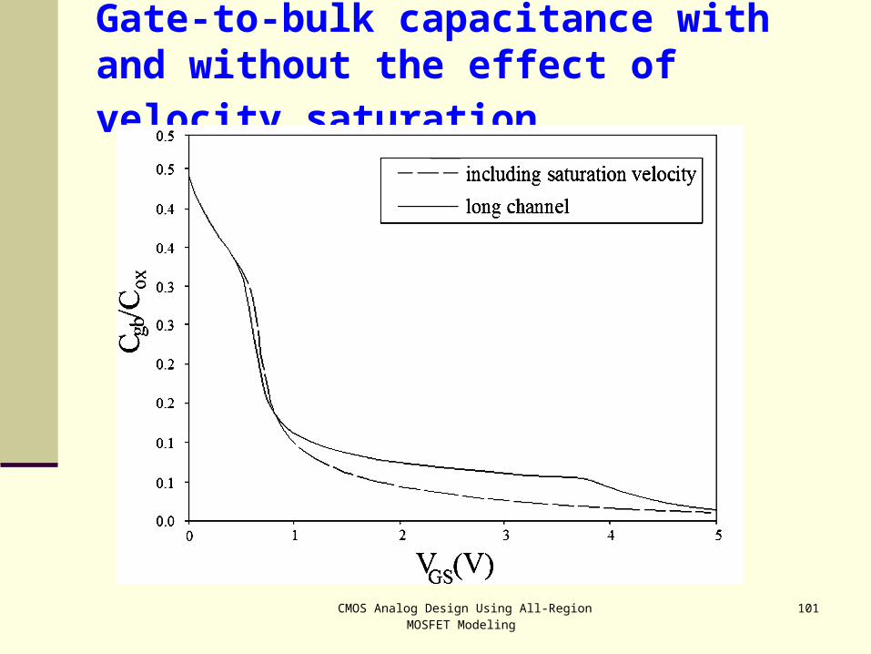
Gate-to-bulk capacitance with and without the effect of velocity saturation