Embed Size (px)
Citation preview
IEEE JOURNAL OF SOLID-STATE CIRCUITS, VOL. 32, NO. 2, FEBRUARY 1997 187
CMOS Active Pixel Image Sensors forHighly Integrated Imaging Systems
Sunetra K. Mendis,Member, IEEE,Sabrina E. Kemeny,Member, IEEE,Russell C. Gee,Member, IEEE,Bedabrata Pain,Member, IEEE,Craig O. Staller, Quiesup Kim,Member, IEEE,
and Eric R. Fossum,Senior Member, IEEE
Abstract—A family of CMOS-based active pixel image sensors(APS’s) that are inherently compatible with the integration of on-chip signal processing circuitry is reported. The image sensorswere fabricated using commercially available 2-�m CMOS pro-cesses and both p-well and n-well implementations were explored.The arrays feature random access, 5-V operation and transistor-transistor logic (TTL) compatible control signals. Methods ofon-chip suppression of fixed pattern noise to less than 0.1%saturation are demonstrated. The baseline design achieved a pixelsize of 40�m� 40 �m with 26% fill-factor. Array sizes of 28 �28 elements and 128� 128 elements have been fabricated andcharacterized. Typical output conversion gain is 3.7�V/e� for thep-well devices and 6.5�V/e� for the n-well devices. Input referredread noise of 28 e� rms corresponding to a dynamic rangeof 76 dB was achieved. Characterization of various photogatepixel designs and a photodiode design is reported. Photoresponsevariations for different pixel designs are discussed.
Index Terms—Active pixel sensor, cameras, CMOS image sen-sor.
I. INTRODUCTION
I N many imaging systems, integration of the image sensorwith circuitry for both driving the image sensor and per-
forming on-chip signal processing is becoming increasinglyimportant. A high degree of electronics integration on thefocal-plane can enable miniaturization of instrument systemsand simplify system interfaces. In addition to good imagingperformance with low noise, no lag, no smear, and goodblooming control, it is desirable to have random access, simpleclocks, and fast readout rates. The development of a CMOS-compatible image sensor technology is an important step forhighly integrated imaging systems since CMOS is well suitedfor implementing on-chip signal processing circuits. CMOS isalso a widely accessible and well-understood technology.
Manuscript received June 20, 1994; revised August 20, 1996. This work wassupported by the JPL Director’s Discretionary Fund, the Advanced ResearchProjects Agency, and the National Aeronautics and Space Administration,Office of Advanced Concepts and Technology.
S. K. Mendis was with the Jet Propulsion Laboratory, California Instituteof Technology, Pasadena, CA 91109 USA. She is now with Hewlett Packard,Palo Alto, CA 94304 USA.
S. E. Kemeny and E. R. Fossum were with Jet Propulsion Laboratory,California Institute of Technology, Pasadena, CA 91109 USA. They are nowwith Photobit, La Crescenta, CA 91214 USA.
R. C. Gee was with Jet Propulsion Laboratory, California Institute ofTechnology, Pasadena, CA 91109 USA. He is now with Intel, Santa Clara,CA 95052 USA.
B. Pain, C. O. Staller, and Q. Kim are with the Jet Propulsion Laboratory,California Institute of Technology, Pasadena, CA 91109 USA.
Publisher Item Identifier S 0018-9200(97)01349-8.
Charge-coupled devices (CCD’s) are currently the dominanttechnology for image sensors. CCD arrays with high fill-factor,small pixel sizes, and large formats have been achieved andsome signal processing operations have been demonstratedwith charge-domain circuits [1]–[3]. However, CCD’s cannotbe easily integrated with CMOS circuits due to additionalfabrication complexity and increased cost. Also, CCD’s arehigh capacitance devices so that on-chip CMOS drive electron-ics would dissipate prohibitively high power levels for largearea arrays (2–3 W). Furthermore, CCD’s need many differentvoltage levels to ensure high charge transfer efficiency. Thereadout rate is limited due to the inherent sequential read out ofCCD’s and the need to achieve nearly perfect charge transferefficiency to maintain signal fidelity. CCD’s also suffer fromsmear and susceptibility to radiation damage.
An active pixel image sensor is defined as an image sensortechnology that has one or more active transistors within thepixel unit cell [4]. This is in contrast to a “passive pixel”approach that uses a simple switch to connect the pixelsignal charge to the column bus capacitance [5]. Active pixelsensors promise lower noise readout, improved scalability tolarge array formats, and higher speed readout compared topassive pixel sensors. Previously demonstrated active pixelsensor (APS) technologies include the amplified MOS imager(AMI) [6], charge modulation device (CMD) [7], bulk chargemodulated device (BCMD) [8], base stored image sensor(BASIS) [9], and the static induction transistor (SIT) [10].Although AMI’s are both CMOS-compatible and amenable tointegration with on-chip circuitry, noise levels and lag can be aproblem due to the uncorrelated reset operation [11]. CMD’s,BCMD’s, and BASIS are also amenable to integration with on-chip circuitry, but can be made CMOS-compatible only withadditional fabrication steps. SIT’s are difficult to integrate withon-chip circuitry and are not CMOS-compatible.
The CMOS active pixel sensors described in this paper areinherently CMOS-compatible. Each pixel unit cell contains animaging element and three transistors for readout, selection,and reset. The imager is read out a row at a time using acolumn parallel readout architecture. The major innovationreported in this paper is the use of intrapixel charge transferto allow correlated-double-sampling (CDS) and on-chip fixedpattern noise (FPN) suppression circuitry located in eachcolumn. These innovations will allow, for the first time,a CMOS image sensor to achieve low noise performancecomparable to a CCD. In all the designs, random access is
0018–9200/97$10.00 1997 IEEE
188 IEEE JOURNAL OF SOLID-STATE CIRCUITS, VOL. 32, NO. 2, FEBRUARY 1997
(a)
(b)
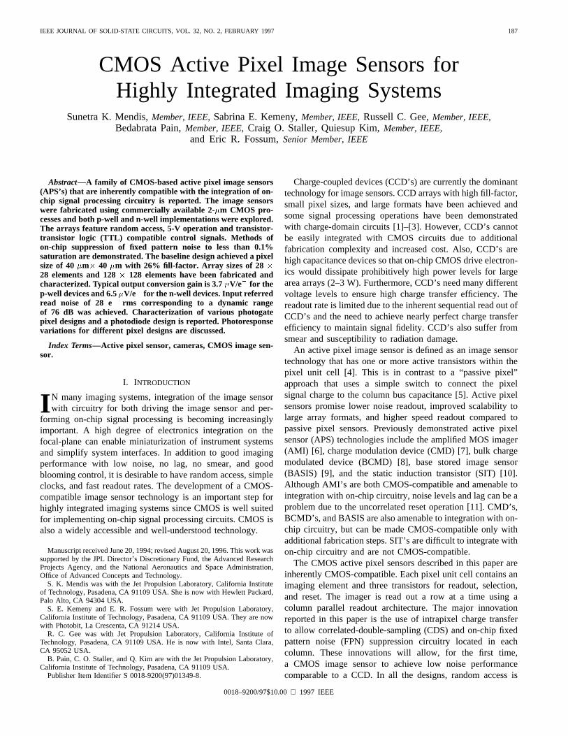
Fig. 1. (a) Schematic of readout circuit and (b) timing for CMOS APS readout.
possible, allowing selective readout of windows of interest.The image sensors are operated with transistor-transistor logic(TTL) clocks and at most two other dc voltages. Theseimage sensors achieve lateral blooming control through properbiasing of the reset transistor. No lag or smear is evident. Thereset and signal levels are read out differentially, allowingCDS to suppress kTC noise, noise, and fixed patternnoise from the pixel. Low noise and high dynamic rangeare achieved. The use of a radiation hard CMOS processto implement the sensor is also a possibility. The CMOSactive pixel image sensors reported here have performancesuitable for many applications including robotics and machinevision, guidance and navigation, automotive applications, andconsumer electronics such as video phones, computer inputs,and home surveillance devices. Future development will leadto scientific sensors suitable for highly integrated imagingsystems for NASA deep space and planetary spacecraft.
This paper presents the design and performance of a familyof CMOS active pixel image sensors. Section II describes thebaseline design, its operation, and noise analysis. Section IIIpresents two fixed pattern noise suppression methods that wereinvestigated. The experimental results of the baseline design
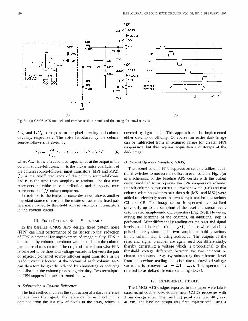
TABLE ITRANSISTOR AND CAPACITOR SIZES
and FPN suppression schemes are presented in Section IV.Section V describes the different pixel unit cell designs ex-plored and compares their performance with the baselinedesign.
II. THE BASELINE CMOS APS
A. Design
A schematic of the baseline pixel design and readout circuitused in the CMOS APS arrays is shown in Fig. 1(a). Thepixel unit cell is shown within the dotted outline. The imagingstructure consists of a photogate (PG) with a floating diffusionoutput (FD) separated by a transfer gate (TX). In essence, asmall surface-channel CCD has been fabricated within eachpixel. The pixel unit cell also contains a reset transistor (MR),the input transistor of the in-pixel source-follower (MIN), anda row selection transistor (MX).
The readout circuit, which is common to an entire columnof pixels, includes the load transistor of the first source-follower (MLN) and two sample-and-hold circuits for storingthe signal level and the reset level. Sampling both the resetand signal levels permits correlated double sampling (CDS)which suppresses reset noise from the floating diffusion nodeof the pixel, and noise and threshold variations fromthe source-follower transistor within the pixel [12]–[14]. Eachsample-and-hold circuit consists of a sample-and-hold switch(MSHS or MSHR) and capacitor (CS or CR) and a columnsource-follower (MP1 or MP2) and column selection transistor(MY1 or MY2) to buffer the capacitor voltages and to drive thehigh capacitance horizontal bus at higher readout speeds. Theload transistors of the column source-followers (MLP1 andMLP2) are common to the entire array of pixels. P-channelsource-followers are used in the column circuit to compensatefor the level shifting of the signal due to the n-channel source-followers within the pixels. The transistor and capacitor sizesare summarized in Table I.
MENDIS et al.: CMOS ACTIVE PIXEL IMAGE SENSORS FOR HIGHLY INTEGRATED IMAGING SYSTEMS 189
(a)
(b)
(c)
(d)
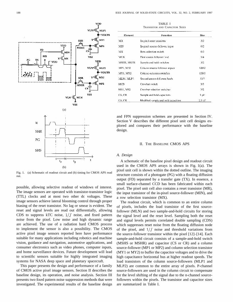
Fig. 2. Operation of CMOS APS (a) signal integration, (b) reset, (c) signalcharge transfer, and (d) signal readout.
B. Operation
The operation of this image sensor is illustrated inFig. 2(a)–(d). The rail voltages VDD and VSS are set at5 V and 0 V, respectively, and the transfer gate TX isbiased at 2.5 V. The load transistors of the in-pixel source-follower and the column source-followers [MLN, MLP1,and MLP2 in Fig. 1(a)] are dc biased at 1.5 V and 2.5 V,respectively. During the signal integration period [Fig. 2(a)],photo-generated electrons are collected under the surface-channel photogate PG biased at 5 V. The reset transistor MR isbiased at 2.5 V to act as a lateral antiblooming drain, allowingexcess signal charge to flow to the reset drain. The row-selection transistor MX is biased off at 0 V. Following signalintegration, an entire row of pixels are read out simultaneously.First, the pixels in the row to be read out are addressed byenabling row selection switch MX. Then the floating diffusionoutput node of the pixel (FD) is reset by briefly pulsing thereset gate of MR to 5 V. This resets FD to approximately 3.5 V
[Fig. 2(b)]. The output of the first source-follower is sampledonto capacitor CR at the bottom of the column by enablingsample-and-hold switch MSHR. Then, PG is pulsed low to0 V, transferring the signal charge to FD [Fig. 2(c)]. Thenew output voltage is sampled onto capacitor CS by enablingsample and hold switch MSHS [Fig. 2(d)]. The stored resetand signal levels are sequentially scanned out through thesecond set of source-followers by enabling column addressswitches MY1 and MY2. This timing sequence is shown inFig. 1(b).
C. Noise Analysis
The main noise sources associated with this system are resetnoise on the floating diffusion node, noise from the inputtransistor of the in-pixel source-follower, dark current shotnoise, reset noise on the sample-and-hold capacitors, and whitenoise and noise from the second source-follower.
The column CDS operation suppresses reset noise on thefloating diffusion node within the pixel. Considering the fre-quency response of the in-pixel source-follower, the outputreferred post-CDS reset noise power can be expressed as
(1)
where and are, respectively, the gains of the in-pixeland column source-followers, is the capacitance of thefloating diffusion node, and are as shown in Fig. 1(b), and
is the cutoff frequency of the in-pixel source-follower. Theoutput referred noise power associated with the in-pixelsource-follower can be expressed as
(2)
where is the flicker noise coefficient of the in-pixel source-follower input transistor (MIN) [15]. Dark current shot noisefrom each pixel can be expressed in output referred noisepower as
(3)
where is the pixel dark current and is the integrationtime. Output referred photon shot noise power can be writtenas
(4)
where represents the input signal.The reset noise on each sample-and-hold capacitor is due to
the white noise in the in-pixel source-follower and the sample-and-hold switches within the bandwidth defined by reset andsignal sampling. The output referred reset noise power is givenby
(5)
where and are, respectively, the sample-and-hold ca-pacitance and the column output bus capacitance. The prefac-tor of two represents noise contribution from the two sample-and-hold branches. The terms within parenthesis,
190 IEEE JOURNAL OF SOLID-STATE CIRCUITS, VOL. 32, NO. 2, FEBRUARY 1997
(a) (b)
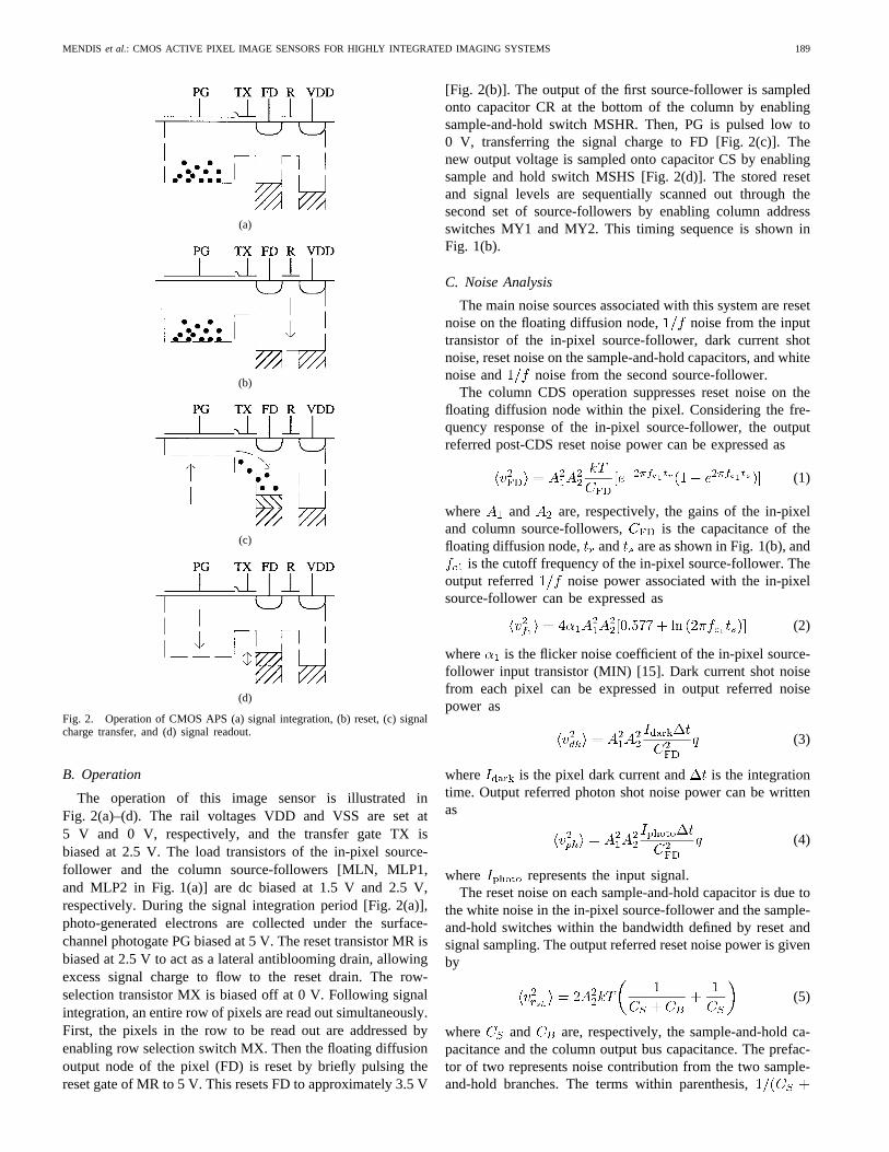
Fig. 3. (a) CMOS APS unit cell and crowbar readout circuit and (b) timing for crowbar readout.
and correspond to the pixel circuitry and columncircuitry, respectively. The noise introduced by the columnsource-followers is given by
(6)
where is the effective load capacitance at the output of thecolumn source-followers, is the flicker noise coefficient ofthe column source-follower input transistors (MP1 and MP2),
is the cutoff frequency of the column source-follower,and is the time from sampling to readout. The first termrepresents the white noise contribution, and the second termrepresents the noise component.
In addition to the temporal noise described above, anotherimportant source of noise in the image sensor is the fixed pat-tern noise caused by threshold voltage variations in transistorsin the readout circuit.
III. FIXED PATTERN NOISE SUPPRESSION
In the baseline CMOS APS design, fixed pattern noise(FPN) can limit performance of the sensor so that reductionof FPN is essential for improvement of image quality. FPN isdominated by column-to-column variations due to the columnparallel readout structure. The origin of the column-wise FPNis believed to be threshold voltage variations between the pairof adjacent p-channel source-follower input transistors in thereadout circuits located at the bottom of each column. FPNcan therefore be greatly reduced by eliminating or reducingthe offsets in the column processing circuitry. Two techniquesof FPN suppression are presented below.
A. Subtracting a Column Reference
The first method involves the subtraction of a dark referencevoltage from the signal. The reference for each column isobtained from the last row of pixels in the array, which is
covered by light shield. This approach can be implementedeither on-chip or off-chip. Of course, an entire dark imagecan be subtracted from an acquired image for greater FPNsuppression, but this requires acquisition and storage of thedark image.
B. Delta-Difference Sampling (DDS)
The second column-FPN suppression scheme utilizes addi-tional switches to measure the offset in each column. Fig. 3(a)is a schematic of the baseline APS design with the outputcircuit modified to incorporate the FPN suppression scheme.In each column output circuit, a crowbar switch (CB) and twocolumn selection switches on either side (MS1 and MS2) wereadded to selectively short the two sample-and-hold capacitorsCS and CR. The image sensor is operated as describedpreviously up to the sampling of the reset and signal levelsonto the two sample-and-hold capacitors [Fig. 3(b)]. However,during the scanning of the columns, an additional step isperformed. After differentially reading out the reset and signallevels stored in each column the crowbar switch ispulsed, thereby shorting the two sample-and-hold capacitorsin the column that is being addressed. The outputs of thereset and signal branches are again read out differentially,thereby generating a voltage which is proportional to thethreshold voltage difference between the two adjacent p-channel transistors By subtracting this reference levelfrom the previous reading, the offset due to threshold voltagevariations is removed This operation isreferred to as delta-difference sampling (DDS).
IV. EXPERIMENTAL RESULTS
The CMOS APS designs reported in this paper were fabri-cated using double-poly, double-metal CMOS processes with2 m design rules. The resulting pixel size was 40m40 m. The baseline design was first implemented using a
MENDIS et al.: CMOS ACTIVE PIXEL IMAGE SENSORS FOR HIGHLY INTEGRATED IMAGING SYSTEMS 191
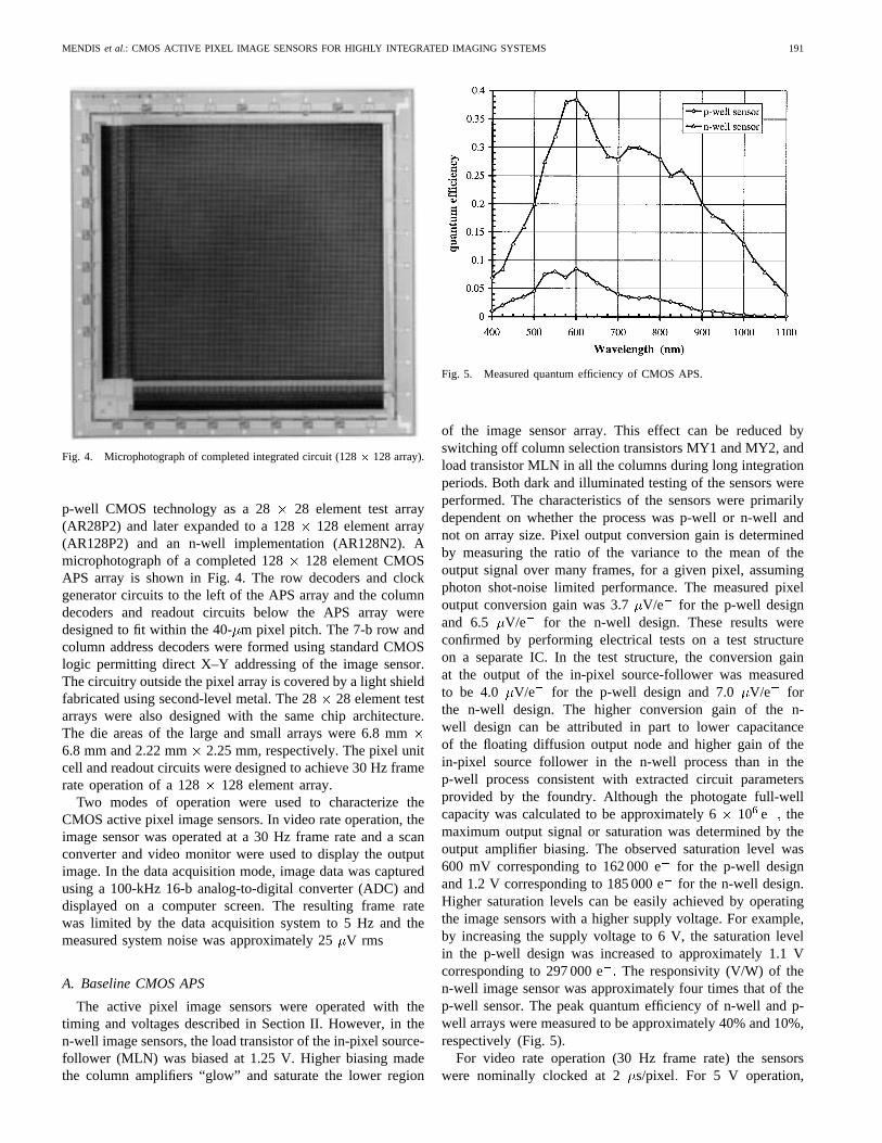
Fig. 4. Microphotograph of completed integrated circuit (128� 128 array).
p-well CMOS technology as a 28 28 element test array(AR28P2) and later expanded to a 128128 element array(AR128P2) and an n-well implementation (AR128N2). Amicrophotograph of a completed 128 128 element CMOSAPS array is shown in Fig. 4. The row decoders and clockgenerator circuits to the left of the APS array and the columndecoders and readout circuits below the APS array weredesigned to fit within the 40-m pixel pitch. The 7-b row andcolumn address decoders were formed using standard CMOSlogic permitting direct X–Y addressing of the image sensor.The circuitry outside the pixel array is covered by a light shieldfabricated using second-level metal. The 2828 element testarrays were also designed with the same chip architecture.The die areas of the large and small arrays were 6.8 mm6.8 mm and 2.22 mm 2.25 mm, respectively. The pixel unitcell and readout circuits were designed to achieve 30 Hz framerate operation of a 128 128 element array.
Two modes of operation were used to characterize theCMOS active pixel image sensors. In video rate operation, theimage sensor was operated at a 30 Hz frame rate and a scanconverter and video monitor were used to display the outputimage. In the data acquisition mode, image data was capturedusing a 100-kHz 16-b analog-to-digital converter (ADC) anddisplayed on a computer screen. The resulting frame ratewas limited by the data acquisition system to 5 Hz and themeasured system noise was approximately 25V rms
A. Baseline CMOS APS
The active pixel image sensors were operated with thetiming and voltages described in Section II. However, in then-well image sensors, the load transistor of the in-pixel source-follower (MLN) was biased at 1.25 V. Higher biasing madethe column amplifiers “glow” and saturate the lower region
Fig. 5. Measured quantum efficiency of CMOS APS.
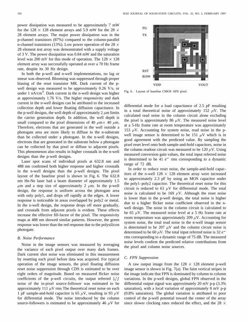
of the image sensor array. This effect can be reduced byswitching off column selection transistors MY1 and MY2, andload transistor MLN in all the columns during long integrationperiods. Both dark and illuminated testing of the sensors wereperformed. The characteristics of the sensors were primarilydependent on whether the process was p-well or n-well andnot on array size. Pixel output conversion gain is determinedby measuring the ratio of the variance to the mean of theoutput signal over many frames, for a given pixel, assumingphoton shot-noise limited performance. The measured pixeloutput conversion gain was 3.7V/e for the p-well designand 6.5 V/e for the n-well design. These results wereconfirmed by performing electrical tests on a test structureon a separate IC. In the test structure, the conversion gainat the output of the in-pixel source-follower was measuredto be 4.0 V/e for the p-well design and 7.0 V/e forthe n-well design. The higher conversion gain of the n-well design can be attributed in part to lower capacitanceof the floating diffusion output node and higher gain of thein-pixel source follower in the n-well process than in thep-well process consistent with extracted circuit parametersprovided by the foundry. Although the photogate full-wellcapacity was calculated to be approximately 610 e themaximum output signal or saturation was determined by theoutput amplifier biasing. The observed saturation level was600 mV corresponding to 162 000 efor the p-well designand 1.2 V corresponding to 185 000 efor the n-well design.Higher saturation levels can be easily achieved by operatingthe image sensors with a higher supply voltage. For example,by increasing the supply voltage to 6 V, the saturation levelin the p-well design was increased to approximately 1.1 Vcorresponding to 297 000 e The responsivity (V/W) of then-well image sensor was approximately four times that of thep-well sensor. The peak quantum efficiency of n-well and p-well arrays were measured to be approximately 40% and 10%,respectively (Fig. 5).
For video rate operation (30 Hz frame rate) the sensorswere nominally clocked at 2 s/pixel For 5 V operation,
192 IEEE JOURNAL OF SOLID-STATE CIRCUITS, VOL. 32, NO. 2, FEBRUARY 1997
power dissipation was measured to be approximately 7 mWfor the 128 128 element arrays and 5.9 mW for the 2828 element arrays. The major power dissipation was in thep-channel transistors (87%) compared to the column-paralleln-channel transistors (13%). Low power operation of the 2828 element test array was demonstrated with a supply voltageof 3 V. The power dissipation was 0.84 mW and the saturationlevel was 200 mV for this mode of operation. The 128128element array was successfully operated at over a 70 Hz framerate, despite its 30 Hz design.
In both the p-well and n-well implementations, no lag orsmear was observed. Blooming was suppressed through properbiasing of the reset transistor MR. Dark current of the p-well design was measured to be approximately 0.26 V/s, orunder 1 nA/cm Dark current in the n-well design was higherat approximately 1.76 V/s. The higher responsivity and darkcurrent in the n-well designs can be attributed to the increasedcollection depth and lower floating diffusion capacitance. Inthe p-well designs, the well depth of approximately 2m limitsthe carrier generation depth. In addition, the well depth issmall compared to the pixel dimensions of 40m 40 m.Therefore, electrons that are generated in the well outside aphotogate area are more likely to diffuse to the n-substratethan be collected under a photogate. In the n-well designs,electrons that are generated in the substrate below a photogatecan be collected by that pixel or diffuse to adjacent pixels.This phenomenon also results in higher crosstalk in the n-welldesigns than the p-well designs.
Laser spot scans of individual pixels at 632.8 nm and488 nm confirmed both higher response and higher crosstalkin the n-well designs than the p-well designs. The pixellayout of the baseline pixel is shown in Fig. 6. The 632.8nm He-Ne laser had a beam diameter of approximately 1.5
m and a step size of approximately 2m. In the p-welldesign, the response is uniform across the photogate areawith only poly1, and drops off rapidly at the edges. A lowerresponse is noticeable in areas overlapped by poly2 or metal.In the n-well design, the response drops off more gradually,and crosstalk from adjacent pixels is evident. These effectsincrease the effective fill-factor of the pixel. The responsivitymaps at 488 nm showed similar patterns. However, the greenresponse was lower than the red response due to the polysiliconphotogate.
B. Noise Performance
Noise in the image sensors was measured by averagingthe variance of each pixel output over many dark frames.Dark current shot noise was eliminated in this measurementby resetting each pixel before data was acquired. For typicaloperation of the image sensors, the pixel floating diffusionreset noise suppression through CDS is estimated to be overeight orders of magnitude. Based on measured flicker noisecoefficients of the p-well circuits, the output referrednoise of the in-pixel source-follower was estimated to beapproximately 111 V rms The theoretical reset noise on each1 pF sample-and-hold capacitor is 65V, resulting in 93 Vfor differential mode. The noise introduced by the columnsource-followers is estimated to be approximately 46V for
Fig. 6. Layout of baseline CMOS APS pixel.
differential mode for a load capacitance of 2.5 pF resultingin a total theoretical noise of approximately 152V. Thecalculated read noise in the column circuit alone excludingthe pixel is approximately 86 V. The measured noise levelat a 5-Hz frame rate at room temperature was approximately153 V. Accounting for system noise, read noise in the p-well image sensor is determined to be 151V which is ingood agreement with the predicted value. By sampling thepixel reset level onto both sample-and-hold capacitors, noise inthe column readout circuit was measured to be 120V. Usingmeasured conversion gain values, the total input referred noiseis determined to be 41 erms corresponding to a dynamicrange of 72 dB.
In order to reduce reset noise, the sample-and-hold capac-itors of the n-well 128 128 element array were increasedto approximately 2.3 pF by using an MOS capacitor underthe poly1–poly2 capacitor. The theoretical reset noise for thiscircuit is reduced to 63 V for differential mode. The totalnoise is calculated to be 169V. Although the reset noiseis lower than in the p-well design, the total noise is higherdue to a higher flicker noise coefficient observed in the n-well design. The noise in the column circuit is calculated tobe 65 V. The measured noise level at a 5 Hz frame rate atroom temperature was approximately 209V. Accounting forsystem noise, the total read noise in the n-well image sensoris determined to be 207V and the column circuit noise isdetermined to be 60V. The total input referred noise is 32 erms corresponding to a dynamic range of 75 dB. The measurednoise levels confirm the predicted relative contributions fromthe pixel and column noise sources.
C. FPN Suppression
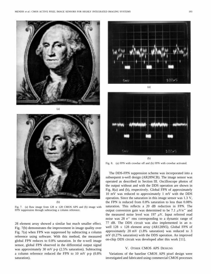
A raw output image from the 128 128 element p-wellimage sensor is shown in Fig. 7(a). The faint vertical stripes inthe image indicate that FPN is dominated by column to columnvariations. In the p-well designs, global FPN observed in thedifferential output signal was approximately 20 mV p-p (3.3%saturation), with a local variation of approximately 8 mV p-p(0.8% saturation). The global variation is attributed to poorcontrol of the p-well potential toward the center of the arraysince slower clocking rates reduced the effect, and the 28
MENDIS et al.: CMOS ACTIVE PIXEL IMAGE SENSORS FOR HIGHLY INTEGRATED IMAGING SYSTEMS 193
(a)
(b)
Fig. 7. (a) Raw image from 128� 128 CMOS APS and (b) image withFPN suppression through subtracting a column reference.
28 element array showed a similar but much smaller effect.Fig. 7(b) demonstrates the improvement in image quality overFig. 7(a) when FPN was suppressed by subtracting a columnreference using software. With this method, the measuredglobal FPN reduces to 0.8% saturation. In the n-well imagesensor, global FPN observed in the differential output signalwas approximately 30 mV p-p (2.5% saturation). Subtractinga column reference reduced the FPN to 10 mV p-p (0.8%saturation).
(a)
(b)
Fig. 8. (a) FPN with crowbar off and (b) FPN with crowbar activated.
The DDS-FPN suppression scheme was incorporated into asubsequent n-well design (AR28NCB). The image sensor wasoperated as described in Section III. Oscilloscope photos ofthe output without and with the DDS operation are shown inFig. 8(a) and (b), respectively. Global FPN of approximately10 mV was reduced to approximately 1 mV with the DDSoperation. Since the saturation in this image sensor was 1.3 V,the FPN is reduced from 0.8% saturation to less than 0.08%saturation. This reflects a 20 dB reduction in FPN. Theoutput conversion gain was determined to be 7.1V/e andthe measured noise level was 197V. Input referred readnoise was 28 e rms corresponding to a dynamic range of77 dB. The DDS circuit was also implemented in an n-well 128 128 element array (AR128N5). Global FPN ofapproximately 20 mV (1.8% saturation) was reduced to 3mV (0.27% saturation) with the DDS operation. An improvedon-chip DDS circuit was developed after this work [11].
V. OTHER CMOS APS DESIGNS
Variations of the baseline CMOS APS pixel design wereinvestigated and fabricated using commercial CMOS processes
194 IEEE JOURNAL OF SOLID-STATE CIRCUITS, VOL. 32, NO. 2, FEBRUARY 1997
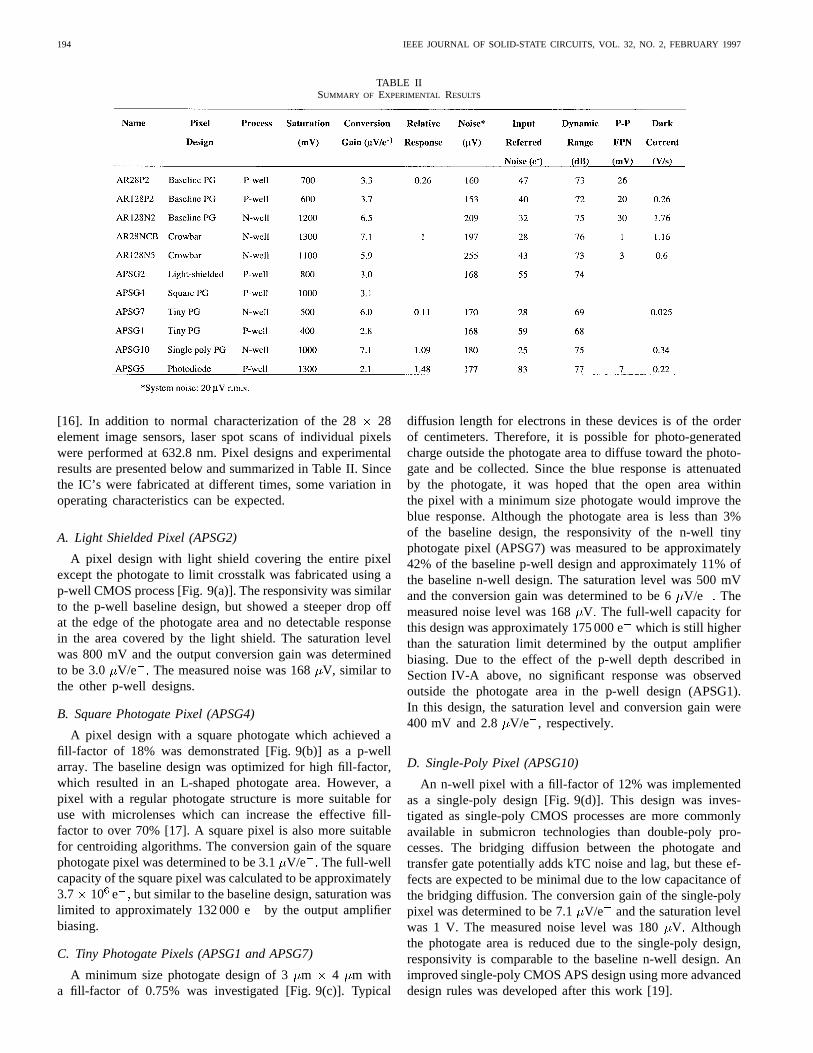
TABLE IISUMMARY OF EXPERIMENTAL RESULTS
[16]. In addition to normal characterization of the 28 28element image sensors, laser spot scans of individual pixelswere performed at 632.8 nm. Pixel designs and experimentalresults are presented below and summarized in Table II. Sincethe IC’s were fabricated at different times, some variation inoperating characteristics can be expected.
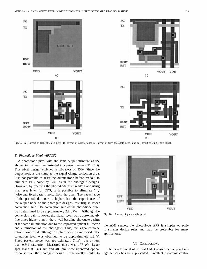
A. Light Shielded Pixel (APSG2)
A pixel design with light shield covering the entire pixelexcept the photogate to limit crosstalk was fabricated using ap-well CMOS process [Fig. 9(a)]. The responsivity was similarto the p-well baseline design, but showed a steeper drop offat the edge of the photogate area and no detectable responsein the area covered by the light shield. The saturation levelwas 800 mV and the output conversion gain was determinedto be 3.0 V/e The measured noise was 168V, similar tothe other p-well designs.
B. Square Photogate Pixel (APSG4)
A pixel design with a square photogate which achieved afill-factor of 18% was demonstrated [Fig. 9(b)] as a p-wellarray. The baseline design was optimized for high fill-factor,which resulted in an L-shaped photogate area. However, apixel with a regular photogate structure is more suitable foruse with microlenses which can increase the effective fill-factor to over 70% [17]. A square pixel is also more suitablefor centroiding algorithms. The conversion gain of the squarephotogate pixel was determined to be 3.1V/e The full-wellcapacity of the square pixel was calculated to be approximately3.7 10 e but similar to the baseline design, saturation waslimited to approximately 132 000 eby the output amplifierbiasing.
C. Tiny Photogate Pixels (APSG1 and APSG7)
A minimum size photogate design of 3m 4 m witha fill-factor of 0.75% was investigated [Fig. 9(c)]. Typical
diffusion length for electrons in these devices is of the orderof centimeters. Therefore, it is possible for photo-generatedcharge outside the photogate area to diffuse toward the photo-gate and be collected. Since the blue response is attenuatedby the photogate, it was hoped that the open area withinthe pixel with a minimum size photogate would improve theblue response. Although the photogate area is less than 3%of the baseline design, the responsivity of the n-well tinyphotogate pixel (APSG7) was measured to be approximately42% of the baseline p-well design and approximately 11% ofthe baseline n-well design. The saturation level was 500 mVand the conversion gain was determined to be 6V/e Themeasured noise level was 168V The full-well capacity forthis design was approximately 175 000 ewhich is still higherthan the saturation limit determined by the output amplifierbiasing. Due to the effect of the p-well depth described inSection IV-A above, no significant response was observedoutside the photogate area in the p-well design (APSG1).In this design, the saturation level and conversion gain were400 mV and 2.8 V/e , respectively.
D. Single-Poly Pixel (APSG10)
An n-well pixel with a fill-factor of 12% was implementedas a single-poly design [Fig. 9(d)]. This design was inves-tigated as single-poly CMOS processes are more commonlyavailable in submicron technologies than double-poly pro-cesses. The bridging diffusion between the photogate andtransfer gate potentially adds kTC noise and lag, but these ef-fects are expected to be minimal due to the low capacitance ofthe bridging diffusion. The conversion gain of the single-polypixel was determined to be 7.1V/e and the saturation levelwas 1 V. The measured noise level was 180V Althoughthe photogate area is reduced due to the single-poly design,responsivity is comparable to the baseline n-well design. Animproved single-poly CMOS APS design using more advanceddesign rules was developed after this work [19].
MENDIS et al.: CMOS ACTIVE PIXEL IMAGE SENSORS FOR HIGHLY INTEGRATED IMAGING SYSTEMS 195
(a) (b)
(c) (d)
Fig. 9. (a) Layout of light-shielded pixel, (b) layout of square pixel, (c) layout of tiny photogate pixel, and (d) layout of single poly pixel.
E. Photodiode Pixel (APSG5)
A photodiode pixel with the same output structure as theabove circuits was demonstrated in a p-well process (Fig. 10).This pixel design achieved a fill-factor of 35%. Since theoutput node is the same as the signal charge collection area,it is not possible to reset the output node before readout toeliminate kTC noise by CDS as in the photogate designs.However, by resetting the photodiode after readout and usingthat reset level for CDS, it is possible to eliminatenoise and fixed pattern noise from the pixel. The capacitanceof the photodiode node is higher than the capacitance ofthe output node of the photogate designs, resulting in lowerconversion gain. The conversion gain of the photodiode pixelwas determined to be approximately 2.1V/e Although theconversion gain is lower, the signal level was approximatelyfive times higher than in the p-well baseline photogate designat the same illumination due to the improved optical fill-factorand elimination of the photogate. Thus, the signal-to-noiseratio is improved although absolute noise is increased. Thesaturation level was observed to be approximately 1.3 V.Fixed pattern noise was approximately 7 mV p-p or lessthan 0.6% saturation. Measured noise was 177V Laserspot scans at 632.8 nm and 488 nm show improved opticalresponse over the photogate designs. Functionally similar to
Fig. 10. Layout of photodiode pixel.
the AMI sensor, the photodiode APS is simpler to scaleto smaller design rules and may be preferable for manyapplications.
VI. CONCLUSIONS
The development of several CMOS-based active pixel im-age sensors has been presented. Excellent blooming control
196 IEEE JOURNAL OF SOLID-STATE CIRCUITS, VOL. 32, NO. 2, FEBRUARY 1997
was achieved and no lag or smear was observed. Both on-chipand off-chip column-FPN reduction schemes were explored.Global FPN was reduced to less than 0.1% using the on-chip DDS circuit. In general, n-well designs showed higherconversion gain and saturation levels than p-well designswhich can be attributed in part to lower capacitance of thefloating diffusion output node and higher gain of the in-pixel source-follower in the n-well process than in the p-wellprocess. P-well designs showed lower responsivity but nocrosstalk between pixels due to the well depth. N-well designsshowed higher responsivity but also showed some crosstalk.Since the noise levels were also higher in the n-well designs,dynamic range was comparable to the p-well designs. Variouspixel designs optimized for limiting crosstalk, integration withmicrolenses, improving optical response, and use of standardsingle-poly CMOS processes without any additional masklevels have been investigated.
Improved readout schemes and methods to further reduceFPN are currently being investigated. Integration of on-chipanalog-to-digital conversion is being explored [18]. Use of0.8- m and 1.2- m CMOS technology can result in higherfill-factor or smaller pixel sizes. The use of microlenses canlikely improve the effective fill-factor. Larger formats canbe implemented with no significant modifications [19]. Highframe rate imaging is also possible with modified transistorsizing and multiport readout. This ongoing research workpaves the way for the development of more complex pixelstructures and the integration of more sophisticated on-chipelectronics in the future.
ACKNOWLEDGMENT
The authors would like to thank M. Ortiz for writingthe image acquisition and display software that was usedin this research. The authors appreciate useful conversationsand encouragement from our colleagues at JPL, especiallyC. Stevens, J. Nakamura, and B. Nixon. The support of V.Sarohia of JPL and G. Johnston of NASA Headquarters isgratefully acknowledged. The research described in this paperwas carried out by the Center for Space MicroelectronicsTechnology, Jet Propulsion Laboratory, California Institute ofTechnology.
Reference herein to any specific commercial product,process, or service by trade name, trademark, manufacturer orotherwise, does not constitute or imply endorsement by theUnited States Government or the Jet Propulsion Laboratory,California Institute of Technology.
REFERENCES
[1] E. R. Fossum, “Architectures for focal-plane image processing,”Opt.Eng., vol. 28, no. 8, pp. 865–871, Aug. 1989.
[2] S. E. Kemeny, E.-S. Eid, S. Mendis, and E. R. Fossum, “Update onfocal-plane image processing research,” inCharge-Coupled Devices andSolid-State Optical Sensors II, Proc. SPIE, vol. 1447, Feb. 1991, pp.243–250.
[3] A. M. Chiang and B. E. Burke, “A high speed digitally programmableCCD transversal filter,”IEEE J. Solid-State Circuits, vol. 18, pp. 745–13,Sept. 1983.
[4] E. R. Fossum, “Active pixel sensors—are CCD’s dinosaurs?,” inCharge-Coupled Devices and Solid-State Optical Sensors III, Proc.SPIE, vol. 1900, Feb. 1993, pp. 2–14.
[5] D. Renshaw, P. Denyer, G. Wang, and M. Lu, “ASIC vision,” inProc.IEEE Custom Integrated Circuits Conf., 1990, pp. 7.3.1–7.3.4.
[6] F. Andohet al., “A 250,000-pixel image sensor with FET amplificationat each pixel for high-speed television cameras,” inISSCC Dig. Tech.Papers, Feb. 1990, pp. 212–213.
[7] M. Ogata, T. Nakamura, K. Matsumoto, R. Ohta, and R. Hyuga, “Asmall pixel CMD image sensor,”IEEE Trans. Electron Devices, vol. 37,pp. 964–971, Apr. 1990.
[8] J. Hynecek, “BCMD—An improved photosite structure for high densityimage sensors,”IEEE Trans. Electron Devices, vol. 38, pp. 1011–1020,May 1991.
[9] N. Tanaka, T. Ohmi, and Y. Nakamura, “A novel bipolar imaging devicewith self-noise reduction capability,”IEEE Trans. Electron Devices, vol.36, pp. 31–37, Jan. 1989.
[10] J. Nisizawa, T. Tamamushi, and T. Ohmi, “Static induction transistor im-age sensor,”IEEE Trans. Electron Devices, vol. ED-26, pp. 1970–1977,Dec. 1979.
[11] R. Nixon, S. Kemeny, C. Staller, and E. Fossum, “128� 128 CMOSphotodiode-type active pixel sensor with on-chip timing, control andsignal chain electronics,” inCharge-Coupled Devices and Solid-StateOptical Sensors V, Proc. SPIE, vol. 2415, Feb. 1995, paper no. 34.
[12] M. White, D. Lampe, F. Blaha, and I. Mack, “Characterization of surfacechannel CCD image arrays at low light levels,”IEEE J. Solid-StateCircuits, vol. SC-9, pp. 1–13, Sept. 1974.
[13] J. Hynecek, “A new device architecture suitable for high-resolution andhigh performance image sensors,”IEEE Trans. Electron Devices, vol.35, no. 5, May 1988.
[14] N. Tanakaet al. “A 310 k Pixel Bipolar Imager (BASIS),” inISSCCDig. Tech. Papers, Feb. 1989, pp. 96–97.
[15] H. Wey and W. Guggenbuhl, “An improved correlated double samplingcircuit for low noise charge-coupled devices,”IEEE Trans. Circuits Syst.,vol. 37, pp. 1559–1565, Dec. 1990.
[16] S. Mendis, S. Kemeny, R. Gee, B. Pain, Q. Kim, and E. Fossum,“Progress in CMOS active pixel image sensors,” inProc. SPIE, vol.2172, Feb. 1994, pp. 19–29.
[17] Y. Sano, T. Nomura, H. Aoki, S. Terakawa, H. Kodama, T. Aoki, andY. Hiroshima, “Submicron spaced lens array process technology for ahigh photosensitivity CCD image sensor,” inIEEE Int. Electron DeviceMeeting Tech. Dig., Dec. 1990, pp. 283–286.
[18] S. Mendis, B. Pain, R. Nixon, and E. Fossum, “Design of a low-light-level image sensor with on-chip sigma-delta analog-to-digital conver-sion,” in Charge-Coupled Devices and Solid-State Optical Sensors III,Proc. SPIE, vol. 1900, Feb. 1993, pp. 15–26.
[19] A. Dickinson, B. Ackland, E.-S. Eid, D. Inglis, and E. Fossum, “A256� 256 CMOS active pixel image sensor with motion detection,” inISSCC Dig. Tech. Papers, Feb. 1995, pp. 226–227.
Sunetra K. Mendis (S’91–M’95) was born in SriLanka. She received the B.S. degree in electricalengineering from Lafayette College, Easton, PA,in 1988 and the M.S. and Ph.D. degrees also inelectrical engineering from Columbia University,New York, NY, in 1990 and 1995, respectively.
From 1991 to 1994 she conducted her doctoralresearch on CMOS active pixel image sensorswith on-chip analog-to-digital conversion at the JetPropulsion Laboratory. From 1994 to 1995 she wasa Member of Technical Staff at AT&T Bell Labs
working on CMOS imagers and capacitive fingerprint sensors. Since 1995 shehas been with the ULSI Research Lab of Hewlett Packard, Palo Alto, CA. Hercurrent research effort is on imaging devices in advanced CMOS processes.
Dr. Mendis is a member of Eta Kappa Nu, Tau Beta Pi, and Phi Beta Kappa.
MENDIS et al.: CMOS ACTIVE PIXEL IMAGE SENSORS FOR HIGHLY INTEGRATED IMAGING SYSTEMS 197
Sabrina E. Kemeny(S’84–M’91) received the A.S.degree from The University of Vermont, Burlington,in 1977. She received the BSEE and MSEE degreesin 1986 and 1987 and the Ph.D. degree in 1991, allin electrical engineering from Columbia University,New York, NY.
She began her professional career as a registerednurse. As a Ph.D. student, her work centered onthe design and implementation of charge-coupleddevice (CCD) image sensors and on-chip imageprocessing using charge domain circuits. In the
summer of 1988, she worked for the Ford Aerospace and CommunicationsCorporation and designed the linear CCD image sensor flown on the MarsObserver Mission. In 1991, she joined the NASA Jet Propulsion Laboratory(JPL) as a Member of the Technical Staff in the Microdevices TechnologySection. At JPL, she worked on VLSI implementation of neural networkcircuits and flew a successful experiment aboard the DoD STRV1 satellitemission. She developed a massively parallel single-chip VLSI processor foroptimal path planning for battlefield management and civilian rescue units.She co-invented the APS technology and became a member of the APS R&DTeam. In 1995 she left JPL to form Photobit and serves as Chief ExecutiveOfficer. She has published more than 26 technical papers and holds threepatents with several patents pending.
While an undergraduate at Columbia, Dr. Kemeny received the HelenRubenstein Outstanding Women of Science Scholarship Award. She wasawarded the JPL/TAP Exceptional Service Award in 1994 for the massivelyparallel single-chip VLSI processor. She also received a NASA Space ActMonetary Award in 1995 while a member of the APS R&D Team.
Russell C. Gee(S’88–M’92) received the B.S. degree in electrical engineeringfrom the University of California, Los Angeles, in 1990. He received the M.S.degree in electrical engineering from the University of California, San Diego,in 1993. His thesis was on the fabrication and characterization of carbon-doped InP/ InGaAs HBT’s.
He was a Member of the Technical Staff at the Jet Propulsion Laboratoryfrom 1992 to 1995 working on the development of CMOS and III-V activepixel sensor technology for visible and IR imaging applications. In 1995, hejoined Intel Corporation in Santa Clara, CA, as a CAD engineer. His currentinterests are in the areas of device physics, CMOS compact modeling, andcompact model parameter extraction methodologies.
Bedabrata Pain (M’95) received the Bachelor of Technology degree in 1986from the Indian Institute of Technology, Kharagpur, India, and the Masters andPh.D. degrees in electrical engineering at Columbia University, New York,NY, in 1989 and 1993, respectively.
In 1993 he joined the Jet Propulsion Laboratory (JPL) as a post-doctoralResearch Associate. Since 1994, he has been a member of technical staffat JPL. Currently, he heads the advanced imager and focal-plane technologygroup at JPL and is involved in research and development of CMOS activepixel sensors, infrared sensors, and integrated charged particle detectors. Hiscurrent research interests include low-noise, low-power mixed analog/digitalVLSI, and integrated sensor technology.
Dr. Pain is the recipient of two NASA achievement awards for his contri-bution to the active pixel sensor technology and the airborne visible/infraredimaging spectrometer.
Craig O. Staller received the B.S. degree in physicsfrom Widener University, Chester, PA, in 1982 andthe M.S. degree, also in physics, from RensselearPolytechnique Institute, Troy, NY, in 1984.
In 1984, he joined General Dynamics Pomona Di-vision working with infrared detectors and infraredtransmitting glass fibers. Since 1985, he has beenwith the Jet Propulsion Laboratory, Pasadena, CA,testing and evaluating infrared, visible, ultravioletand low energy particle detectors and focal planearrays.
Quiesup Kim (M’86) received the B.S., M.S., andPh.D. degrees in physics from the Seoul NationalUniversity, Seoul, Korea, University of Oregon,Eugene, and Oklahoma State University, in 1965,1970, and 1974, respectively.
Since 1980 he has been a Research Scientistat the Jet Propulsion Laboratory, Pasadena, CA.He has been appointed as a Research Advisor forthe National Research Council of the JPL/NASAin 1983. He has published more than 50 papersin lattice dynamics, IR sensors, dielectric materi-
als, pyroelectronics, photoluminescence, Raman and Fourier transformationinfrared spectroscopy, ellipsometry, scanning electron microscopy, and elec-tronic part failure analysis. Recently, he has developed a tool of nondestructivemultipurpose microelectronic advanced laser scanner (MEALS) to applymicron-size laser beams to characterize imaging sensors for improvements inthe design and fabrication. His current research interests include developmentof multispectral monolithic active pixel sensors, noncontact microchanneldevice assessment, and solar power sources for Mars surface applications.
Eric R. Fossum (S’80–M’84–SM’91) received theB.S. in physics and engineering from Trinity Col-lege in 1979 and the Ph.D. in electrical engineeringfrom Yale University, New Haven, CT, in 1984.
He was a member of Columbia University’s Elec-trical Engineering faculty from 1984–1990. At Co-lumbia, he and his students performed researchon CCD focal-plane image processing and highspeed III-V CCD’s. In 1990, he joined the JetPropulsion Laboratory (JPL), California Institute ofTechnology, Pasadena, to manage image sensor and
focal-plane technology research and advanced development. At JPL, he ledthe development of CMOS active pixel sensors and in 1994 was named aSenior Research Scientist. In 1996, he joined Photobit as Chief Scientist, acompany he helped found in 1995. He also serves as Adjunct Professor ofElectrical Engineering at the University of California, Los Angeles. He haspublished over 160 technical papers.
Dr. Fossum has received several awards including the Yale Becton Prizein 1984, the IBM Faculty Development Award in 1984, the National ScienceFoundation Presidential Young Investigator Award in 1986, the JPL Lew AllenAward for Excellence in 1992, and the NASA Exceptional Achievement Medalin 1996. He has organized several conferences including the IEEE Workshopson CCD’s and Advanced Solid-State Image Sensors and the SPIE Conferenceson Infrared Readout Electronics.