Embed Size (px)
Citation preview

October 1998 ! NREL/SR-520-25713
CIS Photovoltaic Technology
Final Technical Report12 January 1997 - 15 April 1998
A.E. Delahoy, J.S. Britt, and Z.J. KissEnergy Photovoltaics, Inc.Lawrenceville, New Jersey
National Renewable Energy Laboratory1617 Cole BoulevardGolden, Colorado 80401-3393A national laboratory of the U.S. Department of EnergyManaged by Midwest Research Institutefor the U.S. Department of Energyunder contract No. DE-AC36-83CH10093

NREL/SR-520-25713
CIS Photovoltaic Technology
Final Technical Report12 January 1997 - 15 April 1998
A.E. Delahoy, J.S. Britt, and Z.J. KissEnergy Photovoltaics, Inc.Lawrenceville, New Jersey
NREL technical monitor: H.S. Ullal
National Renewable Energy Laboratory1617 Cole BoulevardGolden, Colorado 80401-3393A national laboratory of the U.S. Department of EnergyManaged by Midwest Research Institutefor the U.S. Department of Energyunder contract No. DE-AC36-83CH10093
Prepared under Subcontract No. ZAF-5-14142-04
October 1998

This publication was reproduced from the best available copySubmitted by the subcontractor and received no editorial review at NREL
NOTICE
This report was prepared as an account of work sponsored by an agency of the United Statesgovernment. Neither the United States government nor any agency thereof, nor any of their employees,makes any warranty, express or implied, or assumes any legal liability or responsibility for the accuracy,completeness, or usefulness of any information, apparatus, product, or process disclosed, or representsthat its use would not infringe privately owned rights. Reference herein to any specific commercialproduct, process, or service by trade name, trademark, manufacturer, or otherwise does not necessarilyconstitute or imply its endorsement, recommendation, or favoring by the United States government or anyagency thereof. The views and opinions of authors expressed herein do not necessarily state or reflectthose of the United States government or any agency thereof.
Available to DOE and DOE contractors from:Office of Scientific and Technical Information (OSTI)P.O. Box 62Oak Ridge, TN 37831
Prices available by calling (423) 576-8401
Available to the public from:National Technical Information Service (NTIS)U.S. Department of Commerce5285 Port Royal RoadSpringfield, VA 22161(703) 605-6000 or (800) 553-6847orDOE Information Bridgehttp://www.doe.gov/bridge/home.html
Printed on paper containing at least 50% wastepaper, including 10% postconsumer waste

i
Preface
This report describes work performed during the third phase (January 12, 1997 - April 15,1998) of a three-phase, cost-shared subcontract with NREL entitled “CIS PhotovoltaicTechnology”. The subcontract is one component of the NREL Thin Film PartnershipProgram. Remarkably high conversion efficiencies (15 - 17.6%) have beendemonstrated for small area Cu(In,Ga)Se2 devices in the U.S., Europe, and Japan. Amajor objective of this subcontract has been to demonstrate the preparation of highquality CIGS material over large areas (0.43 m2) using novel equipment and processesthat are adaptable to high throughput manufacturing. Using this material, glass-glasslaminated CIGS PV modules have been produced in a pilot line. Research resultsgenerated by other components of the Thin Film Partnership Program and working groupshave been incorporated as needed.
Needless to say, the results described here could not have been achieved without thediligent efforts of the EPV research, engineering and support staff. Other institutions andindividuals have also contributed significantly. At NREL we would like to thank S.Asher, H. Field, A. Franz, R. Matson, A. Mason, and A. Swartzlander for invaluablematerial and device characterization, T. Coutts, T. McMahon, and J. Tuttle for helpfultechnical discussions, and especially R. Noufi for his consistent help to industry toadvance CIGS technology. On the program side, we are indebted to H. Ullal and K.Zweibel for their unflagging interest and support. We have benefited also throughinteraction with the Institute of Energy Conversion/University of Delaware, and throughparticipation in the substrate/Mo/Na working group in collaboration with Colorado StateUniversity, the University of Illinois, International Solar Electric Technology, andLockheed Martin Astronautics.

ii
Summary
Energy Photovoltaics, Inc. has explored novel sequential formation recipes for CIGS thatcan be implemented on a unique pilot line constructed to coat low cost, glass substrates4300 cm2 in area. One particular feature of this line is the use of proprietary linearsources capable of downwards evaporation.
Implementation of a particular CIGS recipe on the pilot line enabled large area modulesto be prepared with efficiencies up to 7.6%. In this recipe, InxGaySez is formed on thesubstrate, followed by metal deposition to supply the Cu, and the resulting precursor isselenized and terminated with additional In and Ga.
Electrical resistance monitoring of the film was shown capable of indicating thetemperature of compound formation and detecting termination. Both IGS and CIGS filmswere analyzed by X-ray diffraction; no binary phases were detected in the CIGS, whilepeaks attributed to CIGS and CGS were observed, as well as CIS. The diffusion andreaction of Ga was studied by deposition of Ga at different temperatures onto Ga-freeprecursors followed by selenization and Auger depth profiling.
The substrate/Mo/Na working group (EPV, ISET, LMA, UI, CSU, NREL) studied Na inMo, and the effect of Na on devices, finding it beneficial except at concentrationsexceeding 0.4%. SIMS profiles suggested segregation of Na towards the Mo interface.
Properties of large area, magnetron sputtered ZnO:Al were: sheet resistance 24 Ω/sq.,transmission 82%, conductivity 440 S cm-1. Preheating of the glass was found to increasethe conductivity.
Devices prepared using a baseline CIGS process averaged 11.7% in efficiency.Considerable efforts were expended studying dark aging effects, light-induced recovery,and cyclic effects in devices utilizing this process, and the effect of moisture on CIGSprior to device fabrication. Later it was discovered that a new CIGS process developed atEPV yielded devices that did not suffer from dark aging effects. This promising processwas termed the FORNAX process. It remains to be implemented on the pilot line.
Modules and minimodules were prepared using a diode-laser-pumped YAG laser for theMo patterning, and mechanical scribing for the subsequent cuts. A 9.7% minimodule wasdemonstrated.
Large area CIGS formation involves the use of linear sources, and thickness profiles werepresented for simple and optimized linear sources. An unencapsulated module producing25 watts (7.65% aperture area efficiency) was produced.
Using a new diagnostic technique, the fill factor of a CIGS module was decomposed intocontributions from the intrinsic device fill factor and ZnO sheet resistance.

iii
Table of Contents
Preface . . . . . . . . . . iSummary . . . . . . . . . . iiTable of Contents . . . . . . . . . iiiList of Figures . . . . . . . . . ivList of Tables . . . . . . . . . . v
Introduction . . . . . . . . . . 11.0 CIGS Deposition and Analysis . . . . . . 2
1.1 Review of General Principles for forming Device-quality CIS or CIGS films . . . . . . . 21.2 Review of General Categories of Absorber Processes . . 31.3 Absorber Formation . . . . . . 4
1.31 Review of EPV’s CIGS formation processes . . 41.32 Resistance monitoring . . . . . 51.33 Effect of the evolution of compound source material . 6
1.4 Structure, Composition and Profiling . . . . 71.41 XRD of CIGS films . . . . . 71.42 Ga composition profiles. . . . . 9
1.5 Findings of the Substrate/Mo/Na Working Group . . 102.0 Zinc Oxide . . . . . . . . . 12
2.1 Deposition and Properties . . . . . 122.2 Doping and Impurities . . . . . . 132.3 Substrate Heating . . . . . . . 13
3.0 Device Studies . . . . . . . . 143.1 Baseline Process . . . . . . . 143.2 Aging and Light-soaking Effects . . . . . 14
3.21 Dark aging . . . . . . 143.22 Recovery via light soaking . . . . 163.23 Cyclic dark aging/light soaking . . . . 193.24 Effect of moisture after CIGS formation . . 203.25 Stability of CIGS prepared by new FORNAX process . 21
4.0 Minimodule Fabrication . . . . . . . 224.1 Purpose and Methods . . . . . . 224.2 Results . . . . . . . . 22
5.0 Module Fabrication and Performance . . . . . 235.1 Processing Steps . . . . . . . 235.2 Linear Source Evaporation . . . . . 245.3 Patterning . . . . . . . . 245.4 Encapssulation . . . . . . . 255.5 Module Performance . . . . . . 275.6 Module Diagnostics . . . . . . 28
References . . . . . . . . . . 29

iv
List of Figures
1.1. Sheet resistance during the formation of CIGS films with and without a termination step.1.2. Auger depth profiles of Ga/(Ga+In) in CIGS films with identical amounts of Ga deposited at various substrate temperatures.1.3. SIMS profile for EPV CIGS on Mo-coated soda-lime glass.2.1. ZnO film characteristics before and after changing the Ar cylinder3.1. Effect of aging on average device efficiency for selenized CIGS films3.2. Device degradation after 75 days storage as a function of the initial Voc x FF.3.3. Average efficiency of runs after 1 hr. light-soaking vs. the average efficiency prior to light-soaking, both normalized to the initial efficiency.3.4. J-V characteristics as a function of light-soaking time.3.5. Experimental diode quality factor and series resistance as a function of light-soaking time.3.6. The improvement of devices upon light-soaking as a function of their Voc, FF product prior to light-soaking.3.7. The improvement of devices upon 1 hr. light-soaking as a function of the amount of degradation in the Voc, FF product after 75 days.3.8. Normalized efficiency of devices from H1725 over the course of time.3.9. Effect of CIGS storage under various conditions prior to CdS/ZnO deposition.3.10. Change in Voc x FF for three sets of FORNAX devices as a function of time. Devices were stored in lab ambient between measurements.4.1. I-V curves of a set of minimodules from run 1724.5.1. Thickness profiles obtained for simple and optimized linear evaporation sources5.2. Monolithically integrated CIGS module showing interconnect scheme and metal foil busbars at module edges.5.3. Layout of CIGS plate prior to lamination.5.4. I-V curve measured by NREL for a 19.7 watt, 3156 cm2 glass-glass gure encapsulated CIGS module.5.5. I-V curve measured in sunlight at EPV for a 25 watt, 7.65% CIGS module.

v
List of Tables
1.1. Effect of the termination step on device characteristics as a function of the fraction of source material remaining.1.2. InGaSe phases observed by XRD.1.3. CIGS phases observed by XRD.1.4. EPMA (20kV) of CIGS films with identical amounts of Ga deposited at various substrate temperatures.1.5. Effect of sodium on CIGS device performance2.1. Properties of ZnO prepared on unheated and pre-heated glass3.1. Average device characteristics for the baseline selenization process.3.2. Ratios of Voc, FF, and Voc x FF after1 hr. light-soaking at AM1.5 relative to their initial values.3.3. Device parameters as a function of light-soaking time.4.1. Photovoltaic parameters of the set of minimodules.5.1 Quality Control Procedures for CIGS Module Fabrication5.2. Comparison of predicted module fill factor (based on diagnostic data) and measured module fill factor for seven CIGS modules

1
Introduction
Thin film photovoltaic modules based on Cu(In,Ga)Se2 have been shown to possessattributes that should enable them to compete effectively with silicon-based modules, andthat should ultimately allow realization of a lower $/Wp cost figure. These attributes arestability, high efficiency, and low materials cost. In addition,
The following guiding principles have been observed by Energy Photovoltaics, Inc. in itsdevelopment of CIS and CIGS technology. Firstly, for safety reasons, solid elementalselenium is used, and not hydrogen selenide; secondly, an all-vacuum process is used toensure even, defect-free coating and impurity control; thirdly, scaleable deposition methodsare used (and where needed, developed); and lastly, the substrate is glass, the flattest,lowest cost substrate available offering structural support and high temperature capability.
2
1.0 CIGS Deposition and Analysis
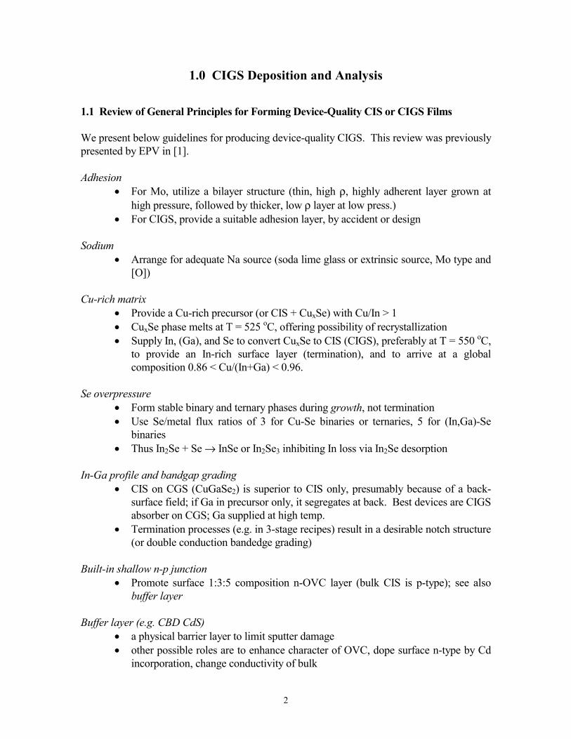
1.1 Review of General Principles for Forming Device-Quality CIS or CIGS Films
We present below guidelines for producing device-quality CIGS. This review was previouslypresented by EPV in [1].
Adhesion• For Mo, utilize a bilayer structure (thin, high ρ, highly adherent layer grown at
high pressure, followed by thicker, low ρ layer at low press.)• For CIGS, provide a suitable adhesion layer, by accident or design
Sodium• Arrange for adequate Na source (soda lime glass or extrinsic source, Mo type and
[O])
Cu-rich matrix• Provide a Cu-rich precursor (or CIS + CuxSe) with Cu/In > 1• CuxSe phase melts at T = 525 oC, offering possibility of recrystallization• Supply In, (Ga), and Se to convert CuxSe to CIS (CIGS), preferably at T = 550 oC,
to provide an In-rich surface layer (termination), and to arrive at a globalcomposition 0.86 < Cu/(In+Ga) < 0.96.
Se overpressure• Form stable binary and ternary phases during growth, not termination• Use Se/metal flux ratios of 3 for Cu-Se binaries or ternaries, 5 for (In,Ga)-Se
binaries• Thus In2Se + Se → InSe or In2Se3 inhibiting In loss via In2Se desorption
In-Ga profile and bandgap grading• CIS on CGS (CuGaSe2) is superior to CIS only, presumably because of a back-
surface field; if Ga in precursor only, it segregates at back. Best devices are CIGSabsorber on CGS; Ga supplied at high temp.
• Termination processes (e.g. in 3-stage recipes) result in a desirable notch structure(or double conduction bandedge grading)
Built-in shallow n-p junction• Promote surface 1:3:5 composition n-OVC layer (bulk CIS is p-type); see also
buffer layer
Buffer layer (e.g. CBD CdS)• a physical barrier layer to limit sputter damage• other possible roles are to enhance character of OVC, dope surface n-type by Cd
incorporation, change conductivity of bulk

3
Compatible transparent conductor• ZnO (0.05 µm i-ZnO + 0.5 µm-ZnO:Al) + optional AR coating
1.2 Review of General Categories of Absorber Formation Processes (for CIS and CIGS)
This section reviews and describes the main categories of absorber formation recipesappearing in the literature. The review was originally presented in [1].
(1) One-stage (coevaporation of all elements at all times)
variations: constant or variable rates (Boeing bilayer; in-line processing)
• at 450 C, Cu + In + Ga + Se → CIGS/CuxSe• at 550 C, with Cu flux↓ CIGS/CuxSe + Cu + In + Ga + Se → CIGS
In↑, Ga↓ = normal gradingditto, then inverse = double grading
cool to 350 C in 20 min. in Se.
(2) Two-stage (coevaporation/termination)
• at 500 C, Cu + In + Ga + Se → CIGS/CuxSe• at 550 C, CIGS/CuxSe + In + Ga + Se → CIGS (no Cu in 2nd stage) overall time
30 min.
(3) Three-stage (sequential delivery of metals with Se/termination)
• at 260 - 300 C, In + Ga + Se → (In,Ga)Sex hexagonal• at 550 C, (In,Ga)Sex + Cu + Se → CIGS/CuxSe (Se prevents In loss)• at 550 C, CIGS/CuxSe + In + Ga + Se → CIGS (10-15% In,Ga added) overall
time 50 min., typically 2.7 µm film, cool to 350 C in 20 min. in Se
Simplifies in situ process controlRadius of In atom < Ga; strain lowered by outdiffusion of In leaving Ga at back. Gaplaced at surface in termination step.
(4) Selenization (sequential delivery of metals without Se/compound formation in Sevapor)
• at low T, (Cu,In) + (Cu,Ga) → CuxIn + CuyGa + Cu + In• + Se during temperature ramp → CuxSe + (In,Ga)ySe• at 450 C, + Se → CIGS
Separates deposition processes from thermal/chemical processesEither H2Se or elemental Se vapor is usedComplex reactions

4
(5) Sequential process with compound source (Se-containing precursor/selenization)
• at low T, precursor formation• at high T, compound formation
Examples:
• 200 C, evaporated InSex (amorphous) + Cu• selenize → CIS (bilayer)
• Cu + InSex
• selenize → CIS (poor adhesion)
Cu front moves through film, CuxSe promotes recrystallizationUse few nm of GaSex to promote adhesion
• (thin adhesion layer) + Cu + InSex + GaSex → CIGS (by XRD)
• GaSex + Cu + InSex → CIS + CIGS (by XRD)
(6) Sequential process with compound source and termination
(7) Stacked elemental layers with selenization
• at RT, metal stack + a-Se (30% excess)• RTP to avoid dewetting of Se at 100 - 200 C; some In loss
At 300 C, Cu4In InSe CuSe CIS 400 C, CuSe CIS 500 C, CIS 550 C, CIS CIGSNa promotes presence of CuSe at higher temperatures
• Other variable gap structures• at 500 C, Cu + Ga + Se → CGS + CuxSe (CGS is small-grained)• at 550 C, + In + Se → CIGS (by XRD) If Ga and In are interchanged, the product is CGS + CIS
1.3. Absorber Formation
1.31 Review of EPV’s CIGS formation processes
Prior to the end of this subcontract, EPV progressed to the third of its absorber formationprocesses. The first process was vacuum selenization of metal precursors. The secondprocess can be described as a sequential process with compound source and termination[2,3]. It is the process by which EPV’s best large area modules have been made, andunless otherwise indicated, it is the subject of most of the work reported here. EPV’s third

5
process has been designated the FORNAX process. It differs in the substrate temperatureduring Cu delivery (among other matters), and results in higher open-circuit voltages andsuperior cell stability.
1.32 Resistance monitoring
Differences in carrier concentration can be used to distinguish between Cu-rich and Cu-poor CIS films, thereby avoiding the continuous monitoring and rate integration of theevaporant fluxes with sophisticated instrumentation. Stoichiometric or Cu-poor CIS filmshave hole concentrations less than 1016 cm-3, while the presence of the Cu2-xSe phase inCu-rich CIS films abruptly raises the hole concentration to 1019 - 1020 cm-3 with profoundeffects on emissivity and electrical conductivity [4]. The former property has beenexploited by Matsushita to develop a temperature monitoring technique to identify thecompositional transition under conditions of constant thermal radiation [5]. In-situconductivity measurements have been performed previously to study the reaction kineticsof CIS and CGS films deposited by a sequential process directly on glass [6]. We haveinvestigated the continuous monitoring of the electrical conductivity during the depositionprocess for its utility in identifying the Cu-rich to Cu-poor transition.
Instead of a specially patterned Mo, the laser-scribed Mo typically employed for modulefabrication was used as the back contact to the CIGS film. Precursors were deposited inthe pilot line on the laser-scribed Mo. Electrical connection to the Mo was made at thesample ends with pressure point contacts. The total electrical resistance is then the sum ofthe resistances of the Mo film and the forming CIGS film across each laser scribe. Thecontribution to the total resistance from the glass was found to be less than 1% at alltemperatures explored, although evidence for sodium ion migration in the glass wasobserved when alternating bias polarity, particularly at temperatures above 400°C.Because the sheet resistance of the Mo film is low (~2 Ω/ ), its contribution to the totalelectrical resistance could also be neglected under most conditions. Resistance wasmonitored directly in a two-wire configuration. An ohmic contact was verified after eachexperiment with a 10V IV measurement.
Two precursors were prepared, one designed to yield only slightly Cu-rich CIGS (A), theother more Cu-rich CIGS (B). Two adjacent samples from precursor A and one samplefrom precursor B were selenized independently from 225°-530°C under a continuous fluxof Se. One of the samples from precursor A was terminated with 500 In while thesubstrate was at 530°C to convert it from Cu-rich to Cu-poor. After selenization, EPMAwas performed at 20 kV on all three samples to determine Cu/(In+Ga). The sheetresistance of the three films, calculated from the scribe dimensions, and the substratetemperature profile are plotted in Figure 1.1 as a function of the selenization time.

6
0 10 20 30 40
0
5
10
15
20
25
30
0
200
400
600
800
1000
1200close shutter
open shutter
temperature (C)
pre. A, term. pre. A, no term. pre. B, no term. substrate temperature
R sh
(kΩ
/sq.)
time (minutes)
Figure 1.1. Sheet resistance during the formation of CIGS films with and without atermination step.
In all cases, there was little change in the sheet resistance up to a temperature of about375°C at which point it increased rapidly until reaching a peak at about 475°C. This isconsistent with reports that CIS forms by the two step process at about 450°C [7]. Thesheet resistance of the CIGS made from the more Cu-rich precursor B (Cu/(In+Ga) = 1.21)was found to increase steadily during the soak at the terminal temperature of 530°C, whilethe sheet resistance of CIGS from precursor A (no termination, Cu/(In+Ga) = 1.07) reachedan equilibrium after 5” at 530°C. This result may be explained by a more defective grainstructure or grain boundaries in Cu-rich CIGS films. It is likely that phase segregationrelated to precursor preparation could lead to similar behavior in Cu-poor CIGS films.
Upon initiating the termination process for precursor A, the sheet resistance rose quicklyand then stabilized before the In source was shuttered. After the shutter was closed, thesheet resistance re-stabilized at a value 1.2x that of the non-terminated film. After cooling to475°C, the sheet resistance of the Cu-poor film was greater than 2x that of the Cu-rich film.Upon cooling to room temperature, the sheet resistances of the terminated (Cu-poor) andnon-terminated (Cu-rich) CIGS films were 5.3 x 10⁷ and 3.0 x 10⁴ Ω/ , respectively. Theterminated film was found to have Cu/(In+Ga) = 0.91. The relatively small difference insheet resistance between Cu-rich and Cu-poor films at high temperature is evidence that thecarrier concentrations are in the intrinsic range.
1.33 Effect of the evolution of compound source material on termination
A proprietary source material deposited by evaporation is used at EPV to form CIGS films.Evolution of the source material has been observed by Auger depth profiling of filmsdeposited by completely evaporating a charge of the source onto cold substrates. Theevolution occurs primarily during the deposition of the last 50% of the charge. The effect

7
of this evolution on device properties has been explored. A charge sufficient for severalterminations was loaded into an evaporation boat. Approximately ½ the charge wasevaporated off before starting this set of experiments. Thus, these experiments representthe last 50% of the source lifetime.
Identical precursor material was selenized and terminated in three successive depositionsand the device properties of the resulting CIGS was evaluated. The termination step wasconducted according to a recipe currently optimized for device efficiency. The best devicecharacteristics from each deposition are listed in the table below. Evaluation of threedevices on each sample show a small improvement in Voc and a larger improvement in fillfactor with successive depositions. It is encouraging that the magnitude of theimprovement in efficiency is relatively small.
Table 1.1. Effect of the termination step on device characteristics as a function of thefraction of source material remaining.
sample # source life%
VocmV
JscmA/cm2
FF%
Eff.%
814B-3H3 33-50 510 34.5 64.5 11.3814B-3H2 17-33 519 33.2 66.1 11.4814B-3H1 0-17 519 35.0 69.6 12.6
1.4 Structure, Composition, and Profiling
1.41 XRD of InGaSe and CIGS films
Two InGaSe films on Mo were analyzed by XRD (see Table 1.2). The first one, 811B, wasa film deposited in the pilot system. The nominal substrate temperature during depositionwas 300°C. The second film, 860-1, was deposited in the R&D reactor at a substratetemperature of 300°C and is about 1200 thick. No additional Se was present during eitherdeposition.
The concentration of In, Ga, and Se in these two films is given at the bottom of Table 1.2.The concentration of 860-1 had to be measured by XPS because of the thinness of the film.The ratio Ga/(Ga+In) as well as Se/(Ga+In+Se) is considerably higher for 811B than 860-1.The only significant peak in sample 811B is attributed to Ga2Se3 (200). Sample 860-1 isessentially amorphous. We believe film 811B can be explained by an evolution of thesource towards more Ga- and Se-rich compounds as the more volatile Se-poor selenides ofIn and Ga (resp.) leave. Whether a base layer with these characteristics is necessary ordesirable for reliable and efficient devices remains to be seen.
8
Table 1.2. InGaSe phases observed by XRD.
comp. 811B 860-1% d rel. int. d rel. int. desig. mat. desig. d
4.1449 2 4.160 2 InSe (004) 4.17003.1553 12 - - Ga2Se3 (200) 3.15002.2265 100 2.2276 100 Mo (110) 2.22471.2962 2 1.2947 2 - -1.2856 2 1.2865 2 Mo (211) 1.28471.2811 2 1.2835 2 - -1.2729 2 1.2796 2 - -1.1135 4 1.1135 4 Mo (220) 1.11291.1105 4 1.1057 2 - -
In 17.6 EPMA 33.2 XPSGa 26.1 EPMA 27.1 XPSSe 56.3 EPMA 39.7 XPS
Two CIGS films were submitted for XRD analysis (see Table 1.3 below). The first one,740B2, was formed entirely within the pilot line and was cut from the module submitted toNREL before encapsulation. This plate had a thin termination with InGaSe (approximately5% of the total In+Ga). The second sample 743b-1r1, was a pilot line precursor cut up andselenized in the R&D reactor with no terminating step. Also included in Table 1.3 is XRDdata from a CIS film (no Ga) selenized in the R&D reactor (H1a) that was taken severalyears ago.
Table 1.3. CIGS phases observed by XRD.
740B2 743b-1r1 H1ad rel.
int.d rel.
int.d rel.
int.desig. mat. desig. d
present - 5.1811 4 5.1945 2 CIS (101) 5.17003.3385 100 3.3434 100 3.3491 100 CIS (112) 3.35103.2501 20 3.2454 15 - - CuIn0.3Ga0.7Se2
(112)3.2500
3.2224 15 - - 3.2227 3 CIS (111) 3.2200present - 2.5225 4 2.5268 2 CIS (211) 2.52802.2308 250 2.2318 104 2.2328 20 Mo (110) 2.22472.0456 45 2.0465 31 2.0496 16 CIS (220) 2.04601.9880 7 1.9870 5 - - CGS (220) 1.98701.7453 20 1.7459 13 1.7467 8 CIS (312) 1.74501.7264 8 1.7233 4 - - CuIn0.7Ga0.3Se2
(312)1.7280
1.4487 5 present - 1.4469 2 CIS (400) 1.44601.3278 5 1.3278 4 1.3296 3 CIS (332) 1.32501.2880 5 1.2874 4 - - Mo (211) 1.28471.1824 5 1.1815 4 1.1842 2 CIS (424) 1.18201.1151 15 1.1159 6 - CIS (512) 1.1130- - 1.1123 4 1.1144 2 Mo (220) 1.1129

9
The first observation is that all the films have a preferred (112) orientation. The samplemade entirely within the pilot line is less oriented than the sample selenized in the R&Dreactor. Neither of these first two Ga-containing samples have as strong a preferredorientation as the CIS film. No discernible peaks were found that can be attributed tobinary phases in any of the films. There are three peaks of significant amplitude found inthe two films with Ga that are not found in the Ga-free CIS film. The three peaks can beattributed to phases of CIGS and CGS. The strongest CGS peak (112. d-3.2100) was notfound but may be buried within the CIS (111) peak at d-3.2200. The CGS (220) peak at d-1.9870 was identified. The peak attributed to CuIn0.7Ga0.3Se2 (312) was identified directlyfrom the JCPDS-ICDD file for that compound. The d- value for CuIn0.3Ga0.7Se2 wasidentified by interpolating between experimental data taken from bulk CIGS samples. Thepresence of a number of phases with various Ga concentrations is not surprising, given thelarge gradients of Ga through these films as detected by Auger. What is surprising is thatany phase exists with a high enough concentration to be identified as a single peak, insteadof appearing as a broad peak with small amplitude, a result of “smearing”.
1.42 Ga composition profiles
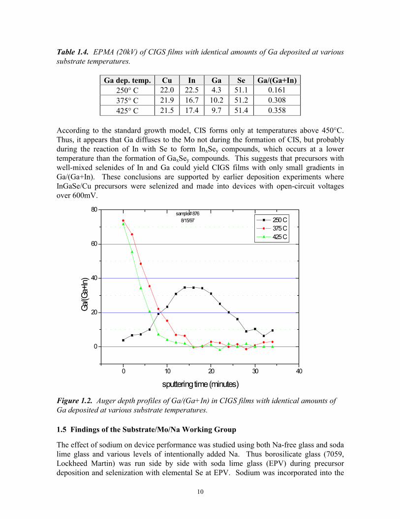
It is generally difficult to incorporate an appreciable amount of Ga in the active region of aCIGS film formed by the simple selenization of metallic precursors. Regardless of itslocation in the precursor stack, Ga has been observed to segregate to the back of the filmand the resulting film is phase-separated with CGS near the Mo electrode and CIS at thefilm surface for Ga/(Ga+In) < 0.6 [8]. This segregation has been thought to occur becauseof the lower temperatures required to form CIS compared to CGS. An experiment wasconducted to test this hypothesis.
A Ga-free precursor was prepared by evaporating 300 In2Se3 onto a 1 ft2 Mo-coatedsubstrate, followed by the sequential evaporation of Cu and In, such that the Cu/In in theprecursor was about 1.20. In2Se3 was used to improve the adhesion of the CIS film to theMo. The plate was cut into smaller sections and the individual pieces were selenized from180°-520°C and in three separate experiments identical amounts of elemental Ga wereevaporated (3 /sec.) while soaking at different temperatures. The amount of Ga evaporatedwas chosen to make the final film slightly Cu-poor. The three soak temperatures examinedwere 250°, 375°, and 425°C. After selenization, a section from each CIGS film wassubmitted for EPMA and Auger depth analysis. The sample that had Ga deposited at250°C had poor adhesion as determined by tape test while the other two samples had goodadhesion.
The EPMA done at 20kV for each of the samples is shown in Table 1.4. The ratios ofGa/(Ga+In) as calculated from the Auger data is shown in Figure 1.2. Based on the Augerdata, the EPMA samples the atomic constituents at about 0.6µm from the surface. The Gaprofile in the sample with Ga deposited at 250°C has a gaussian profile centered in themiddle of the film, while the profiles of the films with Ga deposited at 375° and 425°Cshow the Ga is found primarily at the film surfaces with the concentration decreasingrapidly away from the surface. This implies that the Ga stops diffusing to the back (or In tothe surface) long before the film reaches 450°C.
10
Table 1.4. EPMA (20kV) of CIGS films with identical amounts of Ga deposited at varioussubstrate temperatures.
Ga dep. temp. Cu In Ga Se Ga/(Ga+In)250° C 22.0 22.5 4.3 51.1 0.161375° C 21.9 16.7 10.2 51.2 0.308425° C 21.5 17.4 9.7 51.4 0.358
According to the standard growth model, CIS forms only at temperatures above 450°C.Thus, it appears that Ga diffuses to the Mo not during the formation of CIS, but probablyduring the reaction of In with Se to form InxSey compounds, which occurs at a lowertemperature than the formation of GaxSey compounds. This suggests that precursors withwell-mixed selenides of In and Ga could yield CIGS films with only small gradients inGa/(Ga+In). These conclusions are supported by earlier deposition experiments whereInGaSe/Cu precursors were selenized and made into devices with open-circuit voltagesover 600mV.
0 10 20 30 40
0
20
40
60
808/15/97
sample# 876 250 C 375 C 425 C
Ga/(G
a+In)
sputtering time (minutes)
Figure 1.2. Auger depth profiles of Ga/(Ga+In) in CIGS films with identical amounts ofGa deposited at various substrate temperatures.
1.5 Findings of the Substrate/Mo/Na Working Group
The effect of sodium on device performance was studied using both Na-free glass and sodalime glass and various levels of intentionally added Na. Thus borosilicate glass (7059,Lockheed Martin) was run side by side with soda lime glass (EPV) during precursordeposition and selenization with elemental Se at EPV. Sodium was incorporated into the

11
films by evaporation of Na2S, the atomic % being estimated from the mass evaporated.Devices were fabricated and characterized at EPV, and the films were analyzed by EPMA(A. Swartzlander), SEM (R. Matson), SIMS (A. Rockett), and GIXRD (J. Ryker).
CIGS films on 7059 glass with no extrinsic Na appeared to be small-grained and buckled,with large gaps between the Mo and CIGS. The addition of Na, up to a concentration of0.4%, led to significantly larger grains and less delamination. At 3% Na, the crystallinityhad degraded, the film was small-grained, and delamination was observed.
Device results are summarized in Table 1.5 below. For devices on 7059 glass the fill factorincreased with increasing Na up to 0.4%, while Voc only improved at 3% Na. For deviceson soda lime glass, the low-Na efficiency was higher, and the efficiency declined steadilywith increasing Na.
Table 1.5. Effect of sodium on CIGS device performance
Sample Cu/(In+Ga) Na(atom. %)
Voc(mV)
Jsc(mA/cm2)
FF(%)
Eff.(%)
MM6b1 0.88 0 396 35.8 57.9 8.2MM1a2/EPV2b 0.90/0.89 0.06 404/475 39.1/39.6 65.1/70.5 10.3/13.2MM2a1/EPV3a 0.88/0.88 0.4 398/433 32.7/35.1 67.7/67.4 8.8/10.2MM2a2/EPV2a 0.92/0.90 3.0 454/350 33.1/34.1 57.4/49.3 8.6/5.9
Work elsewhere has shown that Na is easily incorporated at the grain boundaries ofsputtered Mo films, while in CIS, Na decreases the activation energy for electricalconductivity. SIMS analysis (University of Illinois) of Mo sputtered by EPV, ISET, andLMA revealed significant quantities of Na and O, with Na/O relatively constant withineach film. The source of the O is believed to be residual gas in the sputtering system.Annealed (450 °C, 20 mins) Mo/glass substrates yielded ten times more Na. Attemptedselenization of Mo on glass yielded significant selenization depths with H2Se and littleselenization with elemental Se. After H2Se selenization an increase in Na similar to thatresulting from annealing was found.
To study Na in CIS, CIS was coated on Mo/Slglass at EPV and ISET. The EPV samplesexhibited almost an order of magnitude less Na near the outer surface, enhanced Na nearthe Mo interface, and a larger sample-to-sample variation. Possible explanations aredifferent selenization chemistry, or thermal exposure. A typical SIMS profile of EPVCIGS on Mo-coated soda-lime glass is shown in Figure 1.3. The profiles are consistentwith segregation of Na toward the Mo interface, perhaps controlled by CIS microstructure.

12
1
10
100
1000
104
105
106
107
0 500 1000 1500 2000 2500 3000
EP2B2P1.
23 Na63 Cu69 Ga80 Se98 Mo113 InCsO
SIM
S C
ount
s
Sputtering Time (sec)
Figure 1.3. SIMS profile for EPV CIGS on Mo-coated soda-lime glass.
2.0 Zinc Oxide
2.1 Deposition and Properties
The transparent conducting ZnO applied as the final layer in the thin film coating of themodule is magnetron sputtered from ceramic targets of ZnO:Al2O3 in a pulsed, bipolarmode. The sputtering gas is mostly argon, to which a small but carefully controlledconcentration of oxygen is added. The optimal amount of oxygen is a function ofdeposition rate. Film properties obtained on unheated glass substrates (4300 cm2 in area)are: sheet resistance 24 Ω/square, transmission 82% (for films about 0.95 µm inthickness), and conductivity 440 S cm-1. The optimal thickness for use in CIGS modules isfound by plotting properties on iso-efficiency contours for modules [1,3]. If ZnO of qualityequivalent to that produced at EPV by RF sputtering in an R&D machine could beproduced on the large substrates, then a 10% improvement in module fill factor and a 5%improvement in module current could be obtained [9]. A likely route to film improvementwould seem to be substrate heating (see section 2.3 below).
Currently, a sputtering power of 1150 W is used, corresponding to a power density of 28.75W/linear inch of racetrack. The thermal limit of these ceramic targets is not known, but

13
needs to be explored in order to minimize the number of ZnO cathodes used for highvolume manufacturing.
2.2 Doping and Impurities
For large area zinc oxide deposition, sputtering targets containing 1.3%, 1.7% and 2%Al2O3 as the Al dopant source have been utilized. The zinc oxide conductivity increasedfrom 410 S cm-1 to 440 S cm-1 after raising the Al2O3 concentration from 1.3% to 1.7%.
A puzzle related to unusual and inferior quality of RF sputtered ZnO was solved byreplacement of the argon gas cylinder. The sheet resistance and weighted transmission offilms deposited on glass using the new and old gas cylinders are shown in Figure 2.1. At agiven sheet resistance, the new cylinder resulted in superior IR transmission. Impurities inthe old cylinder were almost certainly to blame for the problems. It is believed that watervapor was probably the culprit.
8 10 12 14 16 18 20 22 24 26 280.77
0.78
0.79
0.80
0.81
0.82
0.83
0.84
0.85
0.86
0.87
0.88
0.89
0.90
before cylinder is replaced after cylinder is replaced
Tran
smis
sion
(%)
Rs h( /sq.)
Figure 2.1. ZnO film characteristics before and after changing the Ar cylinder
2.3 Substrate Heating
Although the in-line sputtering system does not contain a substrate heater, nevertheless asuggestive result of the effect of substrate heating was obtained by pre-heating the glasssubstrate in an oven before insertion into the load lock. Experiments were conducted withboth a single piece of glass, and a double stack for improved heat retention. Two scanswere made under the cathode for each substrate, giving a film thickness of about 0.3 µm.A summary of the resulting ZnO film properties is given in Table 2.1 below.

14
Table 2.1. Properties of ZnO prepared on unheated and pre-heated glass
Deposition Rsqohms/sq.
TIR%
conductivity(ohm cm)-1
standard 86 87.6 440pre-heated (single) 67 88.5 500pre-heated (double) 61 89.3 529
Both conductivity and transmission of the ZnO were improved by preheating the glass.Substrate heaters have been designed for a larger in-line sputtering system recentlyconstructed and brought into operation at EPV. It is anticipated that these heaters will beinstalled in the near future.
3.0 Device Studies
3.1 Baseline Process
A substantial amount of effort has been placed on achieving a reproducible process formaking high efficiency CIGS in the R&D reactor by a selenization process that follows theone used in the pilot system as close as possible. Unfortunately, evolution of our standardsource material makes its use in such a process undesirable, so a more reproducible way ofdepositing the base layer has been implemented. Very satisfactory results have beenobtained with the codeposition of Ga and Se. This approach has the advantage high Ga atthe Mo interface, documented in previous reports to be helpful to device fill factor andopen-circuit voltage, as well as excellent reproducibility. The table below summarizes theaverage characteristics of 22 devices evenly distributed over the substrate surface made bythis approach.
Table 3.1. Average device characteristics for the baseline selenization process.
Voc (mV) Jsc (mA/cm2) FF (%) Eff. (%)459 37.0 69.1 11.7
3.2 Aging and Light-soaking Effects
3.21 Dark aging
Longer term stability testing of devices formed by our pilot line process (or slightvariations of) is underway. The vast majority of devices tested thus far suffer from “light-inhibited” degradation. Devices are stored in lab ambient between testings. A number ofruns have been followed for up to 75 days at which time the samples were exposed to a onehour light-soak under approximately AM1.5 illumination in the same setup used for a-Si.After cooling, the devices were re-measured. The results of the first seven runs up to thepoint just before light-soaking are shown in Figure 3.1. Each run consists of about 24devices whose characteristics are averaged. Average efficiencies range from 9-12%.

15
Generally, only the Voc and FF are followed as changes in Jsc have not been observed.After 75 days, efficiencies have dropped to between 83-97% of their initial value. Thechange observed after one week is a good indicator of the potential longer termdegradation.
0 20 40 60 800.80
0.85
0.90
0.95
1.00
1.05
1705 1707 1709 1710 1711 1712 1713
effici
ency
(nor
mali
zed)
days from initial fabricationFigure 3.1. Effect of aging on average device efficiency for selenized CIGS films
Devices with intermediate initial Voc, FF products appear to degrade more than deviceswith greater or smaller products (Fig. 3.2), although there standard deviation for this data isquite large (not shown in the plot). It is possible that the devices with smaller productssuffer from other problems that mask the effect under study.
22 24 26 28 30 32 34 360
5
10
15
20
% d
eg. in
Voc
X F
F (a
fter 7
5 da
ys)
initial Voc x FF
Figure 3.2. Device degradation after 75 days storage as a function of the initial Voc x FF.

16
3.22 Recovery via light soaking
The dark aging effect is reversible upon light-soaking, however the resurrection is notalways complete. Table 3.2 below shows the fraction of the initial Voc, FF and Voc x FF thedevices attained after light-soaking. Three of the seven runs achieved higher averagevalues than those initially measured. It appears that the lower the devices fall, the moredifficult it is to return them to their initial values (Fig. 3.3). In the case of run 1711, nosignificant difference in characteristics was observed between 1 hour and 40 hours of light-soaking. This implies that the degradation is occasionally irreversible. For devices that donot return to their original efficiency after light-soaking, the cause is almost always due to alower Voc. In almost all cases, these devices are the closest to being Cu-rich.
Table 3.2. Ratios of Voc, FF, and Voc x FF after1 hr. light-soaking at AM1.5 relative totheir initial values.
run # Voc FF (VocxFF)
1705 1.005 1.009 1.0141707 0.988 0.969 0.9591709 1.003 1.016 1.0201710 1.018 1.029 1.0481711 0.949 0.987 0.9371712 0.974 0.986 0.9601713 0.969 0.994 0.964
0.80 0.85 0.90 0.95 1.000.90
0.92
0.94
0.96
0.98
1.00
1.02
1.04
1.06
eff.
afte
r lig
ht-s
oaki
ng (n
orm
. to
initi
al e
ff.)
eff. before light-soaking (norm. to initial eff.)
Figure 3.3. Average efficiency of runs after 1 hr. light-soaking vs. the average efficiencyprior to light-soaking, both normalized to the initial efficiency.
17
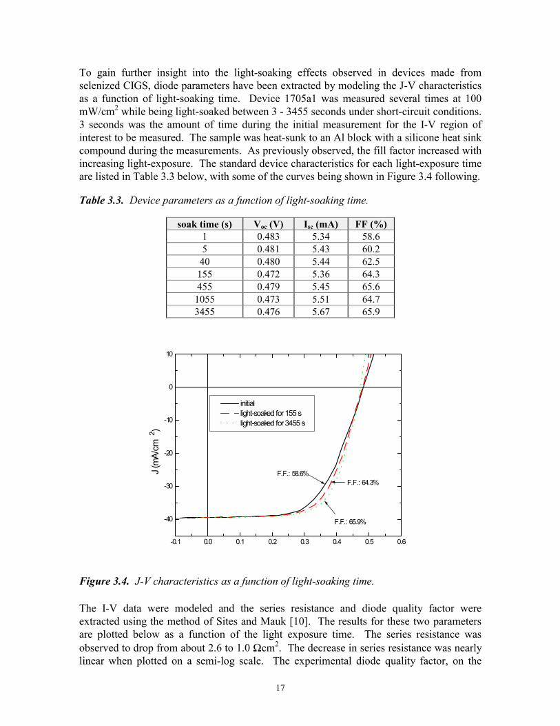
To gain further insight into the light-soaking effects observed in devices made fromselenized CIGS, diode parameters have been extracted by modeling the J-V characteristicsas a function of light-soaking time. Device 1705a1 was measured several times at 100mW/cm2 while being light-soaked between 3 - 3455 seconds under short-circuit conditions.3 seconds was the amount of time during the initial measurement for the I-V region ofinterest to be measured. The sample was heat-sunk to an Al block with a silicone heat sinkcompound during the measurements. As previously observed, the fill factor increased withincreasing light-exposure. The standard device characteristics for each light-exposure timeare listed in Table 3.3 below, with some of the curves being shown in Figure 3.4 following.
Table 3.3. Device parameters as a function of light-soaking time.
soak time (s) Voc (V) Isc (mA) FF (%)1 0.483 5.34 58.65 0.481 5.43 60.240 0.480 5.44 62.5
155 0.472 5.36 64.3455 0.479 5.45 65.61055 0.473 5.51 64.73455 0.476 5.67 65.9
-0.1 0.0 0.1 0.2 0.3 0.4 0.5 0.6
-40
-30
-20
-10
0
10
F.F.: 65.9%
F.F.: 64.3%F.F.: 58.6%
initial light-soaked for 155 s light-soaked for 3455 s
J (m
A/cm
2 )
Figure 3.4. J-V characteristics as a function of light-soaking time.
The I-V data were modeled and the series resistance and diode quality factor wereextracted using the method of Sites and Mauk [10]. The results for these two parametersare plotted below as a function of the light exposure time. The series resistance wasobserved to drop from about 2.6 to 1.0 Ωcm2. The decrease in series resistance was nearlylinear when plotted on a semi-log scale. The experimental diode quality factor, on the

18
other hand, remained nearly constant within experimental error over the measurementinterval.
1 10 100 1000 100000.8
1.0
1.2
1.4
1.6
1.8
2.0
2.2
2.4
2.6
2.8
Rs A
A, R
s (
-cm
2 )
time (s)
Figure 3.5. Experimental diode quality factor and series resistance as a function of light-soaking time.
20 25 30 35-10
0
10
20
30
40
50
60
% im
prov
emen
t
VocxFF prior to light-soaking
Figure 3.6. The improvement of devices upon light-soaking as a function of their Voc, FFproduct prior to light-soaking.
19
-10 0 10 20 30 40-10
0
10
20
30
40
50
60
imp.
in V
ocxF
F af
ter l
ight
-soa
king
(%)
degradation in VocxFF (75 days, %)
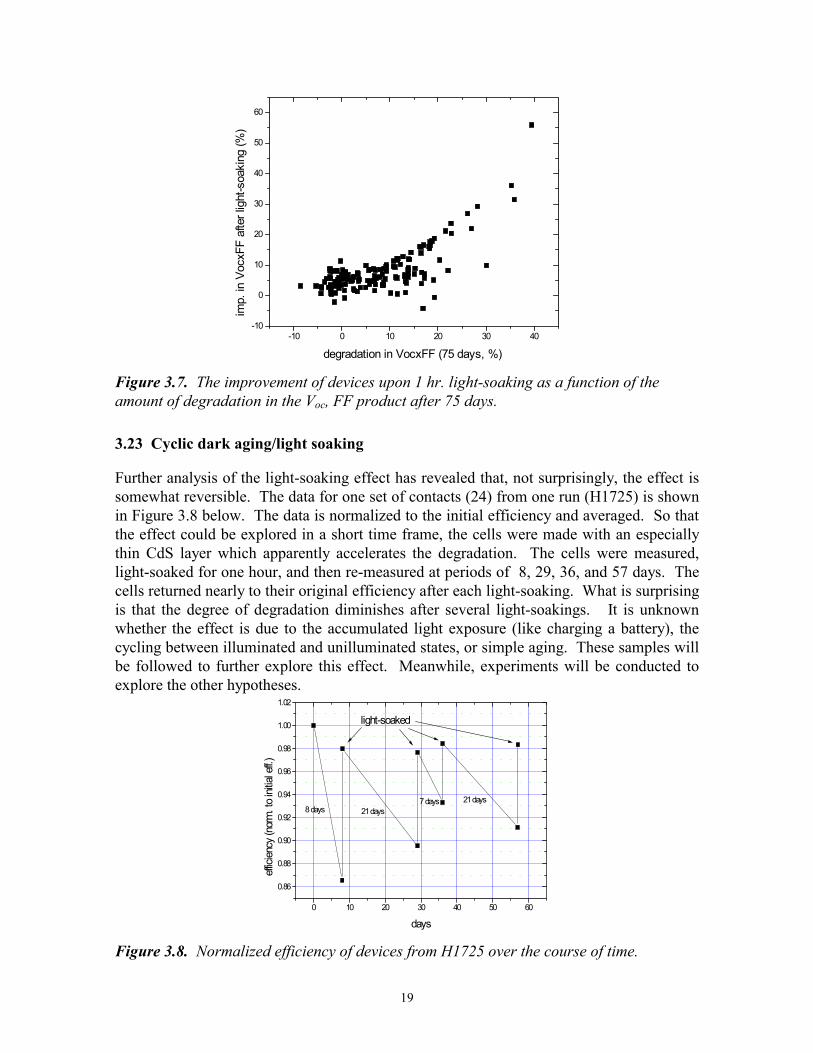
Figure 3.7. The improvement of devices upon 1 hr. light-soaking as a function of theamount of degradation in the Voc, FF product after 75 days.
3.23 Cyclic dark aging/light soaking
Further analysis of the light-soaking effect has revealed that, not surprisingly, the effect issomewhat reversible. The data for one set of contacts (24) from one run (H1725) is shownin Figure 3.8 below. The data is normalized to the initial efficiency and averaged. So thatthe effect could be explored in a short time frame, the cells were made with an especiallythin CdS layer which apparently accelerates the degradation. The cells were measured,light-soaked for one hour, and then re-measured at periods of 8, 29, 36, and 57 days. Thecells returned nearly to their original efficiency after each light-soaking. What is surprisingis that the degree of degradation diminishes after several light-soakings. It is unknownwhether the effect is due to the accumulated light exposure (like charging a battery), thecycling between illuminated and unilluminated states, or simple aging. These samples willbe followed to further explore this effect. Meanwhile, experiments will be conducted toexplore the other hypotheses.
0 10 20 30 40 50 60
0.86
0.88
0.90
0.92
0.94
0.96
0.98
1.00
1.02
21 days7 days21 days8 days
light-soaked
effici
ency
(nor
m. t
o ini
tial e
ff.)
days
Figure 3.8. Normalized efficiency of devices from H1725 over the course of time.

20
Other process parameters that influence the light-inhibited degradation besides the Cu/Inratio (Se flux, temperatures, termination, CdS thickness, etc.) are being examined. In thisregard, cells near the center of the sample area are generally of higher quality than thosearound the perimeter. Another parameter with some apparent control over the change inVoc x FF after a one week period is the CdS thickness. One possibility is that a thicker CdSfilm leads to a higher roomlight Voc (this is fact) sufficient to effect a degree of light-soaking.
3.24 Effect of moisture after CIGS formation
The effect of moisture between the formation of CIGS and further window layer processinghas been explored. CIGS was formed by selenizing and terminating a pilot line precursorin the R&D reactor. The CIGS was cut into pieces and stored for 15 hours under variousconditions before CBD CdS and ZnO were deposited. The four conditions were:
1) stored with desiccant in a sealed container2) stored in room air3) stored at 100% humidity at 20°C in a sealed container4) stored in DI water at room temperature
An adjacent piece of each sample was stored in vacuum during this interval as a controland all pieces were processed together for CdS and ZnO. Devices were made and testedthe same day. The results are shown in Figure 3.9. There was no discernible degradationobserved for the sample stored in desiccant. The other 3 samples showed significantdegradation in the order: room air, 100% humidity, DI water. It may be concluded that theprimary cause of degradation of the devices is related to moisture, not oxygen alone, and isprobably associated with the diffusion of sodium from the glass.
400
420
440
460
480
500
520
540
DI waterstored in
humidity (20C)stored at 100%
room airstored in
dessicantstored with
control
control
control
control
open
-circu
it volt
age (
mV)

21
20
30
40
50
60
70
80
DI waterstored in
humidity (20C)stored at 100%
room airstored in
dessicantstored with
control
controlcontrol
control
fill fa
ctor (
%)
Figure 3.9. Effect of CIGS storage under various conditions prior to CdS/ZnO deposition.
3.25 Stability of CIGS prepared by the new FORNAX process
Three sets of devices from runs H1751, H1754, and H1761 have been tracked to determine thestability of device characteristics. All three CIGS depositions were made by the FORNAXtechnique and window layers were deposited in the standard fashion (CBD CdS, sputteredZnO). Average total area device efficiencies for all three sets were 10-11%. Each datapoint in Figure 3.10 represents the average of 24 devices or slightly fewer (some were damagedduring testing), normalized to their initial Voc x FF. No intentional light-soaking wasemployed. Samples were stored in lab ambient between measurements. Thus far, all threedevice sets have changed less than 2% in Voc x FF during the course of this study, probablywell within the measurement error. Most devices made from selenized CIGS had degradedconsiderably more during a similar period stored in the same location (up to 13%). Thismonitoring will be continued to more fully verify the device stability.
0 10 20 30 40 500.80
0.85
0.90
0.95
1.00
1.05
1751 1754 1761
V oc
x FF
(norm
.)
time (days)
Figure 3.10. Change in Voc x FF for three sets of FORNAX devices as a function of time.Devices were stored in lab ambient between measurements.

22
4.0 Minimodule Fabrication
4.1 Purpose and Methods
To qualify the CIGS process for module manufacture, and to determine the moduleefficiency that can be expected if all films were uniform, minimodules are fabricated.Laser scribing was used for the Mo (see section 5.3), while the 2nd and 3rd scribes (P2 andP3) were performed mechanically on a small x-y table. Modifications were made to themechanical scribing of P2 to expose a wider area by making two scribes offset by 50 µm.The total width of P2 is now about 150µm. This action was taken based on evidence thatseries resistance is introduced if the width of P2 is too narrow (< ~ 60 µm).
4.2 Results
Four test interconnects were made from the CIGS samples of run 1724. The I-Vcharacteristics of the four interconnects are shown in the I-V plot (Figure 4.1) and table(Table 4.1) below.
-2 -1 0 1 2 3 4 5 6 7 8-35
-30
-25
-20
-15
-10
-5
0
5
1724a 1724b 1724c 1724d
J sc
(mA/
cm2 )
volts
Figure 4.1. I-V curves of a set of minimodules from run 1724.
Table 4.1. Photovoltaic parameters of the set of minimodules.
sample areacm2
cells Vocvolts
IscmA
FF%
Pmax
WEff.%
1724a 32.8 16 7.55 63.8 66.0 0.318 9.71724b 33.0 15 6.94 68.1 62.1 0.293 8.91724c 33.6 16 7.33 67.6 61.9 0.307 9.11724d 33.0 15 6.95 68.7 61.2 0.292 8.9

23
Samples 1724b and 1724d were less Cu-poor (and close to Cu-rich at one end) than theother two samples and have slightly lower Voc’s as a result. The higher fill factor of 1724ais at least partly due to higher quality CIGS, but may also be a result of an accident duringZnO deposition (one end of the sample slipped from the mounting plate during depositionand became very hot). The sheet resistance of ZnO films deposited on glass under thesame conditions was 10-12 Ω/sq. Because the sheet resistance of ZnO deposited onCIGS/CdS is typically 20-30% higher, the sheet resistance of ZnO on the interconnects isprobably 12-16 Ω/sq. The effective total area Jsc on all four samples is 31 - 32 mA/cm2
while the Jsc on test devices made in identical runs (with Rsh of 16-18 Ω/sq.) is 37 -38mA/cm2. Allowing for a 10% interconnect area loss, 2-3 mA/cm2 remain to be accountedfor. At least some of this loss may be due to absorption in the slightly thicker ZnO. It waslater discovered that the sputtering gas contained impurities (probably water) that degradedthe optical qualities of the ZnO. This problem was eliminated by replacing the gascylinder. An aperture area efficiency of 9.7% was achieved in this series of samples.
5.0 Module Fabrication and Performance
5.1 Processing Steps
The major processing steps involved in module fabrication are listed in Table 5.1. Some ofthese steps consist of several distinct operations. For example, precursor depositioninvolves multiple depositions of different materials (by sputtering and linear sourceevaporation), and preparation for lamination involves edge isolation, bus bar attachment,hole drilling for lead out, and layout of the EVA film. Also shown in this table are qualitycontrol procedures and characterization methods applicable to each step.
Table 5.1 Quality Control Procedures for CIGS Module Fabrication
Operation QC/Characterization
1. Select glass Determine tin side2. Wash glass Inspection3. Sputter Mo Contactless sheet resistance;
thickness; mechanical stress4. Laser scribe (P1) Check isolation5. Deposit precursor Thickness; mass6. CIGS compound formation Resistance; composition; thickness7. CBD CdS Color; transmission8. Sputter initial ZnO Sheet resistance; diagnostic Voc, Isc
9. Mechanical scribe (P2) Exposure of Mo10. Sputter final ZnO Sheet resistance; thickness; transmission11. Mechanical scribe (P3) Module I-V; diagnostic cell I-V;
QE; thermal imaging; contact res.12. Prepare for lamination Inspection13. Vacuum laminate Module I-V; inspection14. Attach boot and wires Inspection15. Cure Module I-V; label

24
5.2 Linear Source Evaporation
The ability of appropriate linear source designs to deposit a substantially uniform thin filmacross a substrate moving in a direction perpendicular to the axis of the source has beenverified by modeling [1]. For each full pass of the substrate under a source with constantemission strength, the relative thickness distribution in the x direction (x parallel to thesource, and the source extending from x1 to x2) is
t(x) ∝∝∝∝ (x2 - x)/sqrth2 + (x2 - x)2 - (x1 - x)/sqrth2 + (x1 - x)2
where h is the height of the source above the substrate. In Figure 5.1 we show thethickness distribution obtained for a simple 20” source spaced at 2,3,4,5, and 6” from thesubstrate, and the distribution obtained for an optimized source at an appropriate spacing.For the latter 20” source a uniform coating width of about 16” can be obtained. Scaling tolonger sources is straightforward.
EPV linear source design20 inch source, spaced 2 - 6 inches from substrate
0.1
0.3
0.5
0.7
0.9
-13 -11 -9 -7 -5 -3 -1 1 3 5 7 9 11 13
width (inches)
2 " 3" 4" 5" 6" opt. design
Figure 5.1. Thickness profiles obtained for simple and optimized linear evaporationsources
5.3 Patterning
The function of the first patterning step is to separate the Mo into isolated strips. This stepcan be accomplished by laser scribing using the green beam (532 nm) of a frequency-doubled YAG laser. The Mo-coated plate is mounted on an x-y table and translated underthe stationary laser beam. The controlling software is written by EPV. Currently, a fibercoupled, laser diode pumped, Q-switched laser operating in TEM00 mode is employed. An

25
LBO crystal is used for doubling, and an acousto-optic Pockels cell for Q-switching.Verification of electrical isolation between the Mo strips is performed as part of qualitycontrol.
The second and third patterning steps are performed to expose the Mo and to sever theZnO. These steps can be accomplished by mechanical scribing of the CIGS using a bladeshape chosen to minimize the width of the cut. During Phase III, various upgrades weremade to the system so that the scribing operation is now semi-automated. These upgradesincluded addition of a computer system and user-interface software, closed-loop servomotor indexing of position, and addition of safety limit switches for over travel protection.The improvements allow for more accurate positioning of the knives (≈10µm/step), higherthroughput, and better plate-plate repeatability.
5.4 Encapsulation
Preparation of the patterned CIGS plate for lamination includes removal of films aroundthe periphery of the substrate, attachment of Al foil bus bars by ultrasonic welding, anddrilling of the substrate for lead out. The interconnect scheme and foil location is shown inFigure 5.2.
Figure 5.2. Monolithically integrated CIGS module showing interconnect scheme andmetal foil busbars at module edges.
The layout of the monolithically-interconnected plate prior to lamination is shown inFigure 5.3. The standard plate area is 4294 cm2. Lamination is performed in a vacuumlaminator using fast cure EVA in sheet form. Electrical connections to the module aremade via two strain-relieved, insulated wires that are connected to the foils under a siliconeboot for environmental protection. The module is frameless, and is mounted via four Alextrusions glued to the back of the substrate glass. This encapsulation scheme is similar tothe one used by EPV in its fabrication of tandem junction a-Si modules.

26
Layout of CIGS Plate before Encapsulation
Figure 5.3. Layout of CIGS plate prior to lamination.
27
5.5 Module Performance
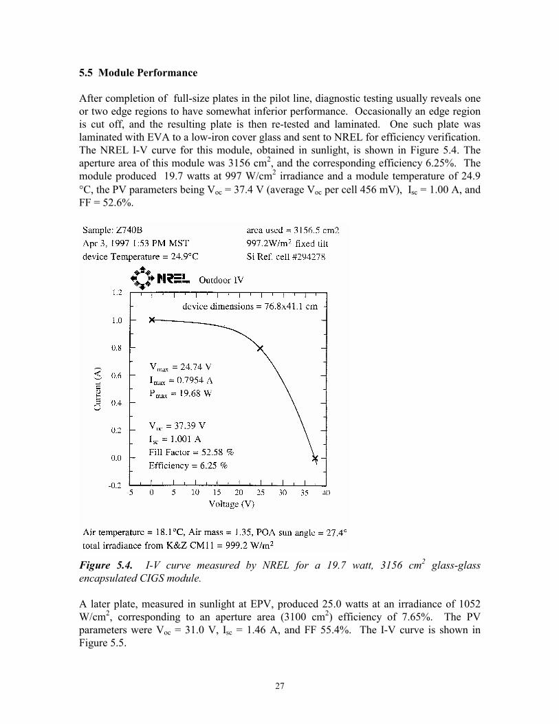
After completion of full-size plates in the pilot line, diagnostic testing usually reveals oneor two edge regions to have somewhat inferior performance. Occasionally an edge regionis cut off, and the resulting plate is then re-tested and laminated. One such plate waslaminated with EVA to a low-iron cover glass and sent to NREL for efficiency verification.The NREL I-V curve for this module, obtained in sunlight, is shown in Figure 5.4. Theaperture area of this module was 3156 cm2, and the corresponding efficiency 6.25%. Themodule produced 19.7 watts at 997 W/cm2 irradiance and a module temperature of 24.9°C, the PV parameters being Voc = 37.4 V (average Voc per cell 456 mV), Isc = 1.00 A, andFF = 52.6%.
Figure 5.4. I-V curve measured by NREL for a 19.7 watt, 3156 cm2 glass-glassencapsulated CIGS module.
A later plate, measured in sunlight at EPV, produced 25.0 watts at an irradiance of 1052W/cm2, corresponding to an aperture area (3100 cm2) efficiency of 7.65%. The PVparameters were Voc = 31.0 V, Isc = 1.46 A, and FF 55.4%. The I-V curve is shown inFigure 5.5.

28
0 5 1 0 1 5 2 0 2 5 3 0 3 50
5 0 0
1 0 0 0
1 5 0 0
s u n l i g h t 1 0 5 2 W / m 2V o c = 3 0 . 9 5 VI s c = 1 4 5 8 m AF F = 5 5 . 4 %P m a x = 2 5 . 0 WA p . a r e a = 3 1 0 0 c m 2E f f . = 7 . 6 5 %
C I G S m o d u le Z C 7 0 9 7C
ur
re
nt
(m
A)
V o l t a g e ( V )
Figure 5.5. I-V curve measured in sunlight at EPV for a 25 watt, 7.65% CIGS module.
5.6 Module Diagnostics
A new diagnostic technique was developed at EPV in order to be able to map the quality ofthe CIGS device across a large monolithic plate in a non-destructive manner [1-3]. Themethod is illustrated in Figure 5.6. The entire module is illuminated and driven through itsI-V curve by a computer-controlled bipolar supply, while three probes pick up voltagesfrom which local cell current and voltage values can be inferred. The positioning of theprobes is shown in the inset to the figure. The intrinsic I-V curve of the cell on which the2nd and 3rd probes are placed is obtained by plotting V23 = V2 - V3 (proportional to cellcurrent) versus V12 = V1 - V2 (cell voltage). The fill factor of the cell is then calculated inthe usual way. Prior to invention of this technique, determination of the fill factor at agiven location on a plate required destructive scribing of the films to isolate a smalldiagnostic cell. If, as a reasonable first approximation, it is assumed that the module short-circuit current distributes evenly across the plate, then the local sheet resistance of the zincoxide can be calculated from the measured V23 as Rsq = 2V23 /[Jsc(x3
2-x22)], where x3 and
x2 are the distances of probes 3 and 2 from the edge of the cell.
The technique has been used to map Voc and FF across the surface of large area, patternedCIGS plates and has been instrumental in detecting gradients in performance [2]. Thetechnique has also been applied to decompose the measured fill factor of a CIGS moduleinto the intrinsic device fill factor and the effect of ZnO sheet resistance. Existingdiagnostic data concerning the local device fill factor for seven CIGS modules wereaveraged across each plate (see Table 5.2). Next, from computer modeling of module fillfactor (at 1000 W/m2) versus ZnO sheet resistance, fill factor reduction factors (defined asFF( Rsq )/FF( Rsq = 0 ), where Rsq is the ZnO sheet resistance) were calculated. Thepredicted module fill factor was then calculated as diagnostic fill factor times fill factorreduction factor. From Table 5.2 it can be seen that this calculation, using the average

29
diagnostic fill factor and diagnostic ZnO sheet resistance determined by the newtechniques, indeed closely predicted the actual measured module fill factor. This confirmsour ability to quantify the relative contributions of intrinsic device fill factor and ZnO sheetresistance in determining the fill factor of a module. This understanding is an importanttool for further module optimization.
Table 5.2. Comparison of predicted module fill factor (based on diagnostic data) andmeasured module fill factor for seven CIGS modules
Averagediagnostic FF
(%)
diagnosticZnO Rsq
(ohms/sq.)
FF reductionfactor
predictedmodule FF
(%)
measuredmodule FF
(%)62.0 27 0.83 51.4 54.563.5 36 0.77 49.0 50.858.0 30 0.81 47.2 46.657.3 38 0.76 43.8 46.560.8 51 0.70 42.6 41.950.2 33 0.79 39.8 40.443.4 54 0.68 29.4 31.1
References
1. Delahoy, A.E. and Meyers, P.V., “Thin-Film PV Modules: Manufacturing Technology andIssues,” Tutorial III, 26th IEEE Photovoltaic Specialists Conference, September 29, 1997.
2. Britt, J.S., Delahoy, A.E., and Kiss, Z.J., “Pilot Production of CIGS Photovoltaic Modules,” Proceedings of the 26th IEEE Photovoltaic Specialists Conference, Anaheim (IEEE, 1997) pp. 335-338.3. Britt, J.S., Delahoy, A.E., and Kiss, Z.J., “Large Area Coating of CIGS and ZnO for Photovoltaics,” Proceedings of the 14th European Photovoltaic Solar Energy Conference, Barcelona (H.S. Stephens, 1997) pp. 1287-1290.4. Noufi, R., Axton, R., Herrinton, C., and Deb, S., Appl. Phys. Lett. 45 (1984), 668.5. Kohara, N., Negami, T., Nishitani, M., and Wada, T., Jpn. J. Appl. Phys. 34, 2 (1995) L1141.6. Zwiegart, S., Schock, H.W., and Powalla, M., Proceedings of the 14th European Photovoltaic Solar Energy Conference, Barcelona, Spain, (H.S. Stephens, 1997) pp.1254-1257.7. Yamanaka, S., McCandless, B. E., Birkmire, R. W., Proceedings of the 23rd IEEE Photovoltaic Specialists Conference, 1993, 607.8. Marudachalam, M., Birkmire, R., Schultz, J., and Yokimcus, T., 1st World Conference on Photovoltaic Energy Conversion (1994) 234.9. Delahoy, A.E., Britt, J.S., Kiss, Z.J. (1997) “CIS Photovoltaic Technology.” Annual Technical Progress Report, NREL/SR-520-23194. 38pp. Available NTIS: Order No. DE 97050822.10. Sites, J.R., and Mauk, P.H., Solar Cells, 27 (1989) 411-417.

REPORT DOCUMENTATION PAGE Form ApprovedOMB NO. 0704-0188
Public reporting burden for this collection of information is estimated to average 1 hour per response, including the time for reviewing instructions, searching existing data sources,gathering and maintaining the data needed, and completing and reviewing the collection of information. Send comments regarding this burden estimate or any other aspect of thiscollection of information, including suggestions for reducing this burden, to Washington Headquarters Services, Directorate for Information Operations and Reports, 1215 JeffersonDavis Highway, Suite 1204, Arlington, VA 22202-4302, and to the Office of Management and Budget, Paperwork Reduction Project (0704-0188), Washington, DC 20503.
1. AGENCY USE ONLY (Leave blank) 2. REPORT DATEOctober 1998
3. REPORT TYPE AND DATES COVEREDFinal Technical Report
4. TITLE AND SUBTITLECIS Photovoltaic Technology; Final Technical Report
6. AUTHOR(S)A.E. Delahoy, J.S. Britt, and Z.J. Kiss
5. FUNDING NUMBERS
C: ZAF-5-14142-04TA: PV905001
7. PERFORMING ORGANIZATION NAME(S) AND ADDRESS(ES)Energy Photovoltaics, Inc.276 Bakers Basin RoadLawrenceville, NJ 08648
8. PERFORMING ORGANIZATIONREPORT NUMBER
9. SPONSORING/MONITORING AGENCY NAME(S) AND ADDRESS(ES)National Renewable Energy Laboratory1617 Cole Blvd.Golden, CO 80401-3393
10. SPONSORING/MONITORINGAGENCY REPORT NUMBER
SR-520-25713
11. SUPPLEMENTARY NOTES
NREL Technical Monitor: H.S. Ullal12a. DISTRIBUTION/AVAILABILITY STATEMENT
National Technical Information ServiceU.S. Department of Commerce5285 Port Royal RoadSpringfield, VA 22161
12b. DISTRIBUTION CODE
13. ABSTRACT (Maximum 200 words)This report describes work performed by Energy Photovoltaics, Inc. (EPV) during the third phase of a three-phase, cost-sharedsubcontract. Researchers at EPV explored novel sequential formation recipes for CIGS that can be implemented on a unique pilot lineconstructed to coat low-cost, glass substrates 4300 cm2 in area; implemented a particular CIGS recipe on the pilot line that enabledlarge-area modules to be prepared with efficiencies up to 7.6%; and performed electrical resistance monitoring of the film that provedcapable of indicating the temperature of compound formation and detecting termination. The substrate/Mo/Na working group (whichincluded EPV, NREL, and others) studied Na in Mo and the effect of Na on devices, and found it beneficial except at concentrationsexceeding 0.4%. Researchers determined the following properties of large-area, magnetron-sputtered ZnO:Al: sheet resistance 24Ω/sq., transmission 82%, conductivity 440 S cm-1; and preheating the glass increases the conductivity. Devices prepared using abaseline CIGS process averaged 11.7% in efficiency. Modules and minimodules were prepared using a diode-laser-pumped yttrium-aluminum-garnet laser for the Mo patterning and mechanical scribing for the cuts. Large-area CIGS formation involves the use oflinear sources, and thickness profiles were presented for simple and optimized linear sources. An unencapsulated module producing25 watts (7.65% aperture-area efficiency) was produced. Using a new diagnostic technique, the fill factor of a CIGS module wasdecomposed into contributions from the intrinsic device fill factor and ZnO sheet resistance.
15. NUMBER OF PAGES39
14. SUBJECT TERMS
photovoltaics ; Thin Film PV Partnership Program ; Cu(In,Ga)Se2 ; CIGS ; module fabrication ;module performance ; sodium
16. PRICE CODE
17. SECURITY CLASSIFICATIONOF REPORTUnclassified
18. SECURITY CLASSIFICATIONOF THIS PAGEUnclassified
19. SECURITY CLASSIFICATIONOF ABSTRACTUnclassified
20. LIMITATION OF ABSTRACT
UL
NSN 7540-01-280-5500 Standard Form 298 (Rev. 2-89)Prescribed by ANSI Std. Z39-18
298-102


![Miranda J. Delahoy - sgp.org.pe · • greater risk of injury, disease, and death due to more intense heat waves and fires [very high confidence] • increased risk of under-nutrition](https://img.dokumen.tips/doc/110x75/600a588b5e8d9b1915137b13/miranda-j-delahoy-sgporgpe-a-greater-risk-of-injury-disease-and-death-due.jpg)


![On Optimization Design of College Mathematics ... · School Party Construction and ideological Education [J] .2010364. [5] Z.J. Zhang and Z.Y. Nie. The application practice and thinking](https://img.dokumen.tips/doc/110x75/5f80e432e5f4d31c3c7cc7d3/on-optimization-design-of-college-mathematics-school-party-construction-and.jpg)