Embed Size (px)
Citation preview
© 2012-2019 NXP B.V.
NXP SemiconductorsChip Errata
This document details the silicon errata known at the time of publication for the i.MX 6Solo/6DualLite multimedia applications processors.For details on part marking and silicon revision level identification and comparison, see the “Ordering Information” section of the i.MX 6Solo/6DualLite Applications Processor Data Sheet for your device.
For details on the ARM® configuration used on this chip (including ARM module revisions), please see the “Platform configuration” section of the “ARM Cortex®-A9 MPCore Platform” chapter of the i.MX 6Solo/6DualLite Applications Processor Reference Manual.
IMX6SDLCERev. 7, 03/2019
Chip Errata forthe i.MX 6Solo/6DualLite
Chip Errata for the i.MX 6Solo/6DualLite, Rev. 7, 03/2019
2 NXP Semiconductors
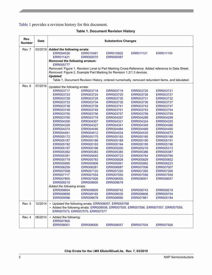
Table 1 provides a revision history for this document.Table 1. Document Revision History
Rev.Number Date Substantive Changes
Rev. 7 03/2019 Added the following errata:ERR004536 ERR010481 ERR010822 ERR011121 ERR011100ERR011421 ERR050070 ERR050087
Removed the following erratum:ERR005777
Removed: Figure 1, Revision Level to Part Marking Cross-Reference. Added reference to Data Sheet.Removed: Figure 2, Example Part Marking for Revision 1.2/1.3 devices.Updated:
Table 1, Document Revision History, ordered numerically, removed redundant items, and tabulated.
Rev. 6 07/2016 Updated the following errata:ERR003717 ERR003718 ERR003719 ERR003720 ERR003721ERR003723 ERR003724 ERR003725 ERR003726 ERR003727ERR003728 ERR003729 ERR003730 ERR003731 ERR003732ERR003733 ERR003734 ERR003735 ERR003736 ERR003737ERR003738 ERR003739 ERR003741 ERR003743 ERR003747ERR003748 ERR003749 ERR003751 ERR003753 ERR003754ERR003755 ERR003756 ERR003757 ERR003758 ERR003759ERR003760 ERR003778 ERR004297 ERR004298 ERR004299ERR004300 ERR004307 ERR004321 ERR004324 ERR004325ERR004326 ERR004327 ERR004341 ERR004349 ERR004366ERR004374 ERR004446 ERR004484 ERR004489 ERR004490ERR004491 ERR004512 ERR004534 ERR004535 ERR004573ERR005172 ERR005175 ERR005183 ERR005185 ERR005186ERR005187 ERR005188 ERR005189 ERR005190 ERR005191ERR005192 ERR005193 ERR005194 ERR005195 ERR005196ERR005197 ERR005198 ERR005200 ERR005216 ERR005313ERR005382 ERR005383 ERR005385 ERR005386 ERR005387ERR005391 ERR005645 ERR005723 ERR005764 ERR005766ERR005778 ERR005783 ERR005828 ERR005829 ERR005852ERR005895 ERR005908 ERR005991 ERR005992 ERR006223ERR006259 ERR006281 ERR006687 ERR007006 ERR007007ERR007008 ERR007122 ERR007220 ERR007265 ERR007266ERR007117 ERR007554 ERR007555 ERR007556 ERR007559ERR007805 ERR007926 ERR008000 ERR008001 ERR008057ERR009219 ERR009605 ERR009678
Added the following errata:ERR009604 ERR009605 ERR009742 ERR009743 ERR009219ERR009858 ERR009165 ERR009535 ERR009606 ERR009704ERR009596 ERR009678 ERR008990 ERR007881 ERR005184
Rev. 5 12/2014 • Updated the following errata: ERR008057, ERR005768 • Added the following errata: ERR008506, ERR007555, ERR007556, ERR007557, ERR007559,
ERR007573, ERR007575, ERR007577
Rev. 4 06/2014 • Added the following:ERR007805ERR008001 ERR008000 ERR008057 ERR007554 ERR007926
Chip Errata for the i.MX 6Solo/6DualLite, Rev. 7, 03/2019
NXP Semiconductors 3
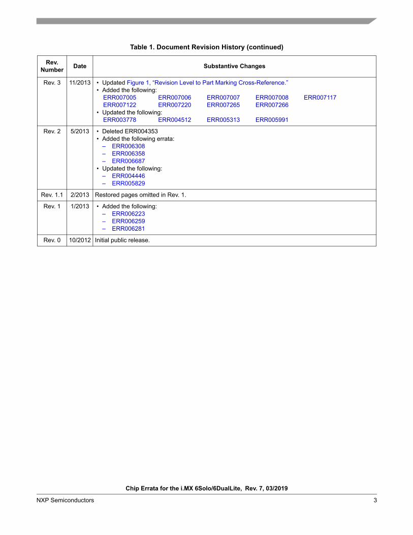
Rev. 3 11/2013 • Updated Figure 1, “Revision Level to Part Marking Cross-Reference.” • Added the following:
ERR007005 ERR007006 ERR007007 ERR007008 ERR007117ERR007122 ERR007220 ERR007265 ERR007266
• Updated the following:ERR003778 ERR004512 ERR005313 ERR005991
Rev. 2 5/2013 • Deleted ERR004353 • Added the following errata:
– ERR006308– ERR006358– ERR006687
• Updated the following:– ERR004446– ERR005829
Rev. 1.1 2/2013 Restored pages omitted in Rev. 1.
Rev. 1 1/2013 • Added the following: – ERR006223– ERR006259– ERR006281
Rev. 0 10/2012 Initial public release.
Table 1. Document Revision History (continued)
Rev.Number Date Substantive Changes
Chip Errata for the i.MX 6Solo/6DualLite, Rev. 7, 03/2019
4 NXP Semiconductors
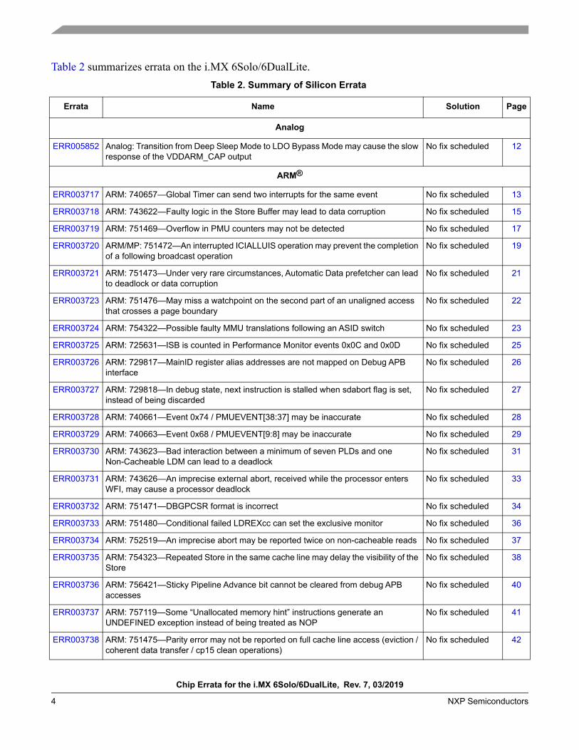
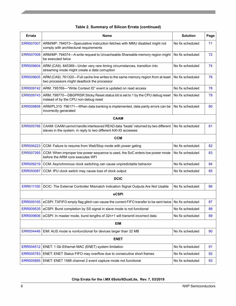
Table 2 summarizes errata on the i.MX 6Solo/6DualLite.Table 2. Summary of Silicon Errata
Errata Name Solution Page
Analog
ERR005852 Analog: Transition from Deep Sleep Mode to LDO Bypass Mode may cause the slow response of the VDDARM_CAP output
No fix scheduled 12
ARM®
ERR003717 ARM: 740657—Global Timer can send two interrupts for the same event No fix scheduled 13
ERR003718 ARM: 743622—Faulty logic in the Store Buffer may lead to data corruption No fix scheduled 15
ERR003719 ARM: 751469—Overflow in PMU counters may not be detected No fix scheduled 17
ERR003720 ARM/MP: 751472—An interrupted ICIALLUIS operation may prevent the completion of a following broadcast operation
No fix scheduled 19
ERR003721 ARM: 751473—Under very rare circumstances, Automatic Data prefetcher can lead to deadlock or data corruption
No fix scheduled 21
ERR003723 ARM: 751476—May miss a watchpoint on the second part of an unaligned access that crosses a page boundary
No fix scheduled 22
ERR003724 ARM: 754322—Possible faulty MMU translations following an ASID switch No fix scheduled 23
ERR003725 ARM: 725631—ISB is counted in Performance Monitor events 0x0C and 0x0D No fix scheduled 25
ERR003726 ARM: 729817—MainID register alias addresses are not mapped on Debug APB interface
No fix scheduled 26
ERR003727 ARM: 729818—In debug state, next instruction is stalled when sdabort flag is set, instead of being discarded
No fix scheduled 27
ERR003728 ARM: 740661—Event 0x74 / PMUEVENT[38:37] may be inaccurate No fix scheduled 28
ERR003729 ARM: 740663—Event 0x68 / PMUEVENT[9:8] may be inaccurate No fix scheduled 29
ERR003730 ARM: 743623—Bad interaction between a minimum of seven PLDs and one Non-Cacheable LDM can lead to a deadlock
No fix scheduled 31
ERR003731 ARM: 743626—An imprecise external abort, received while the processor enters WFI, may cause a processor deadlock
No fix scheduled 33
ERR003732 ARM: 751471—DBGPCSR format is incorrect No fix scheduled 34
ERR003733 ARM: 751480—Conditional failed LDREXcc can set the exclusive monitor No fix scheduled 36
ERR003734 ARM: 752519—An imprecise abort may be reported twice on non-cacheable reads No fix scheduled 37
ERR003735 ARM: 754323—Repeated Store in the same cache line may delay the visibility of the Store
No fix scheduled 38
ERR003736 ARM: 756421—Sticky Pipeline Advance bit cannot be cleared from debug APB accesses
No fix scheduled 40
ERR003737 ARM: 757119—Some “Unallocated memory hint” instructions generate an UNDEFINED exception instead of being treated as NOP
No fix scheduled 41
ERR003738 ARM: 751475—Parity error may not be reported on full cache line access (eviction / coherent data transfer / cp15 clean operations)
No fix scheduled 42
Chip Errata for the i.MX 6Solo/6DualLite, Rev. 7, 03/2019
NXP Semiconductors 5
ERR003739 ARM: 751470—Imprecise abort on the last data of a cache linefill may not be detected
No fix scheduled 43
ERR003741 ARM/PL310: 729815—The “High Priority for SO and Dev reads” feature can cause Quality of Service issues to cacheable read transactions
No fix scheduled 44
ERR003743 ARM/PL310: 754670—A continuous write flow can stall a read targeting the same memory area
No fix scheduled 45
ERR004324 ARM/MP: 761319—Ordering of read accesses to the same memory location may not be ensured
No fix scheduled 46
ERR004325 ARM/MP: 764369—Data or unified cache line maintenance operation by MVA may not succeed on an Inner Shareable memory region
No fix scheduled 47
ERR004326 ARM/MP: 761321—MRC and MCR are not counted in event 0x68 No fix scheduled 49
ERR004327 ARM/MP: 764319—Read accesses to DBGPRSR and DBGOSLSR may generate an unexpected UNDEF
No fix scheduled 50
ERR005175 ARM/MP: 771221—PLD instructions may allocate data in the Data Cache regardless of the Cache Enable bit value
No fix scheduled 51
ERR005183 ARM/MP: 771224—Visibility of Debug Enable access rights to enable/disable tracing is not ensured by an ISB
No fix scheduled 52
ERR005185 ARM/MP: 771225—Speculative cacheable reads to aborting memory region clear the internal exclusive monitor, may lead to livelock
No fix scheduled 53
ERR005187 ARM/MP: 771223—Parity errors on BTAC and GHB are reported on PARITYFAIL[7:6], regardless of the Parity Enable bit value
No fix scheduled 55
ERR005198 ARM/PL310: 780370—DATAERR, TAGERR, and Tag parity errors are incorrectly sampled by the eviction buffer, leading to data corruption
No fix scheduled 56
ERR005200 ARM/MP: 765569—Prefetcher can cross 4 KB boundary if offset is programmed with value 23
No fix scheduled 59
ERR005382 ARM/MP: 775419—PMU event 0x0A (exception return) might count twice the LDM PC ^ instructions with base address register write-back
No fix scheduled 60
ERR005383 ARM/MP: 775420—A data cache maintenance operation that aborts, followed by an ISB and without any DSB in-between, might lead to deadlock
No fix scheduled 61
ERR005385 ARM/MP: 782772—A speculative execution of a Load-Exclusive or Store-Exclusive instruction after a write to Strongly Ordered memory might deadlock the processor
No fix scheduled 62
ERR005386 ARM/MP: 782773—Updating a translation entry to move a page mapping might erroneously cause an unexpected translation fault
No fix scheduled 64
ERR005387 ARM/MP: 782774—A spurious event 0x63, “STREX passed,” can be reported on an LDREX that is preceded by a write to Strongly Ordered memory region
No fix scheduled 66
ERR005391 ARM: Debug CTI interrupt can cause a system deadlock when power gating the core No fix scheduled 67
ERR006259 ARM: Debug/trace functions (PMU, PTM and ETB) are disabled with absence of JTAG_TCK clock after POR
No fix scheduled 68
ERR007006 ARM/MP:794072-- Short loop including a DMB instruction might cause a denial of service
No fix scheduled 69
Table 2. Summary of Silicon Errata (continued)
Errata Name Solution Page
Chip Errata for the i.MX 6Solo/6DualLite, Rev. 7, 03/2019
6 NXP Semiconductors
ERR007007 ARM/MP: 794073—Speculative instruction fetches with MMU disabled might not comply with architectural requirements
No fix scheduled 71
ERR007008 ARM/MP: 794074—A write request to Uncacheable Shareable memory region might be executed twice
No fix scheduled 72
ERR009604 ARM (CA9): 845369—Under very rare timing circumstances, transition into streaming mode might create a data corruption
No fix scheduled 74
ERR009605 ARM (CA9): 761320—Full cache line writes to the same memory region from at least two processors might deadlock the processor
No fix scheduled 76
ERR009742 ARM: 795769—“Write Context ID” event is updated on read access No fix scheduled 78
ERR009743 ARM: 799770—DBGPRSR Sticky Reset status bit is set to 1 by the CPU debug reset instead of by the CPU non-debug reset
No fix scheduled 79
ERR009858 ARM/PL310: 796171—When data banking is implemented, data parity errors can be incorrectly generated
No fix scheduled 80
CAAM
ERR005766 CAAM: CAAM cannot handle interleaved READ data “beats” returned by two different slaves in the system, in reply to two different AXI-ID accesses
No fix scheduled 81
CCM
ERR006223 CCM: Failure to resume from Wait/Stop mode with power gating No fix scheduled 82
ERR007265 CCM: When improper low-power sequence is used, the SoC enters low power mode before the ARM core executes WFI
No fix scheduled 83
ERR009219 CCM: Asynchronous clock switching can cause unpredictable behavior No fix scheduled 84
ERR050087 CCM: IPU clock switch may cause loss of clock output No fix scheduled 85
DCIC
ERR011100 DCIC: The External Controller Mismatch Indication Signal Outputs Are Not Usable No fix scheduled 86
eCSPI
ERR009165 eCSPI: TXFIFO empty flag glitch can cause the current FIFO transfer to be sent twice No fix scheduled 87
ERR009535 eCSPI: Burst completion by SS signal in slave mode is not functional No fix scheduled 88
ERR009606 eCSPI: In master mode, burst lengths of 32n+1 will transmit incorrect data No fix scheduled 89
EIM
ERR004446 EIM: AUS mode is nonfunctional for devices larger than 32 MB No fix scheduled 90
ENET
ERR004512 ENET: 1 Gb Ethernet MAC (ENET) system limitation No fix scheduled 91
ERR005783 ENET: ENET Status FIFO may overflow due to consecutive short frames No fix scheduled 92
ERR005895 ENET: ENET 1588 channel 2 event capture mode not functional No fix scheduled 93
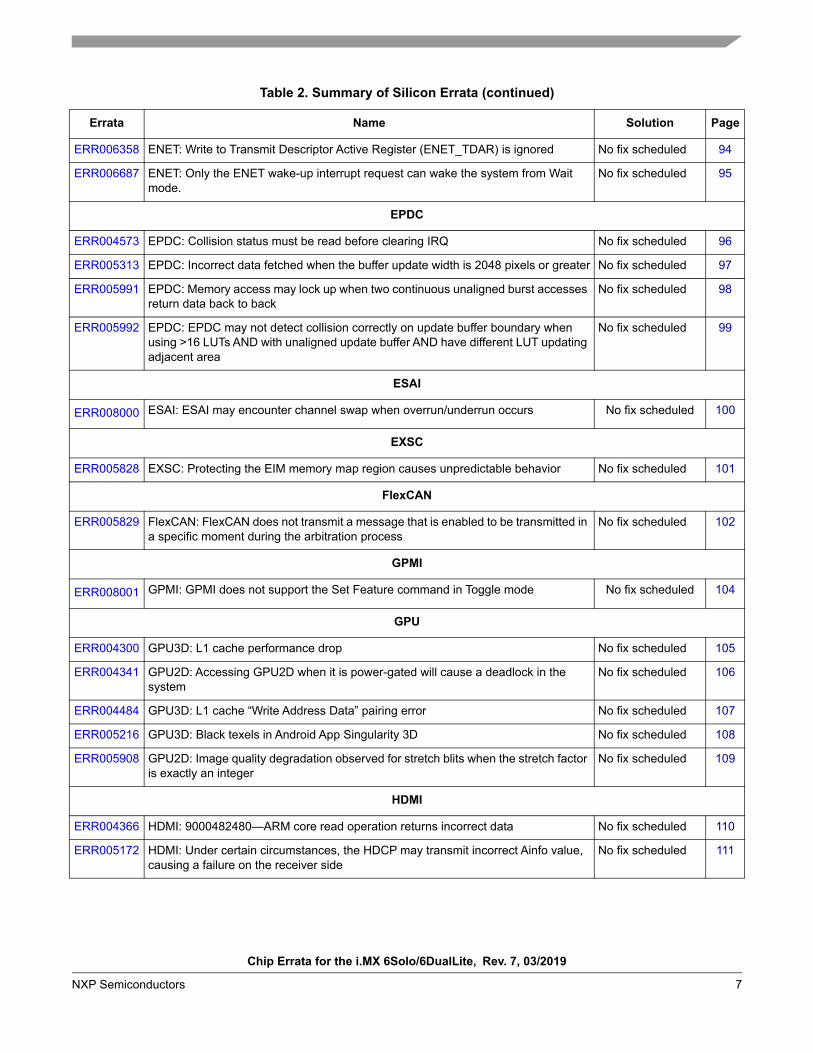
Table 2. Summary of Silicon Errata (continued)
Errata Name Solution Page
Chip Errata for the i.MX 6Solo/6DualLite, Rev. 7, 03/2019
NXP Semiconductors 7
ERR006358 ENET: Write to Transmit Descriptor Active Register (ENET_TDAR) is ignored No fix scheduled 94
ERR006687 ENET: Only the ENET wake-up interrupt request can wake the system from Wait mode.
No fix scheduled 95
EPDC
ERR004573 EPDC: Collision status must be read before clearing IRQ No fix scheduled 96
ERR005313 EPDC: Incorrect data fetched when the buffer update width is 2048 pixels or greater No fix scheduled 97
ERR005991 EPDC: Memory access may lock up when two continuous unaligned burst accesses return data back to back
No fix scheduled 98
ERR005992 EPDC: EPDC may not detect collision correctly on update buffer boundary when using >16 LUTs AND with unaligned update buffer AND have different LUT updating adjacent area
No fix scheduled 99
ESAI
ERR008000 ESAI: ESAI may encounter channel swap when overrun/underrun occurs No fix scheduled 100
EXSC
ERR005828 EXSC: Protecting the EIM memory map region causes unpredictable behavior No fix scheduled 101
FlexCAN
ERR005829 FlexCAN: FlexCAN does not transmit a message that is enabled to be transmitted in a specific moment during the arbitration process
No fix scheduled 102
GPMI
ERR008001 GPMI: GPMI does not support the Set Feature command in Toggle mode No fix scheduled 104
GPU
ERR004300 GPU3D: L1 cache performance drop No fix scheduled 105
ERR004341 GPU2D: Accessing GPU2D when it is power-gated will cause a deadlock in the system
No fix scheduled 106
ERR004484 GPU3D: L1 cache “Write Address Data” pairing error No fix scheduled 107
ERR005216 GPU3D: Black texels in Android App Singularity 3D No fix scheduled 108
ERR005908 GPU2D: Image quality degradation observed for stretch blits when the stretch factor is exactly an integer
No fix scheduled 109
HDMI
ERR004366 HDMI: 9000482480—ARM core read operation returns incorrect data No fix scheduled 110
ERR005172 HDMI: Under certain circumstances, the HDCP may transmit incorrect Ainfo value, causing a failure on the receiver side
No fix scheduled 111
Table 2. Summary of Silicon Errata (continued)
Errata Name Solution Page
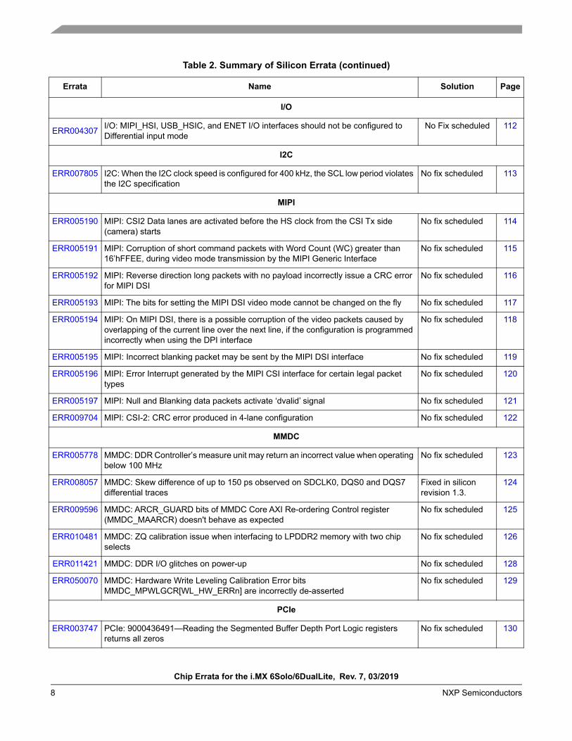
Chip Errata for the i.MX 6Solo/6DualLite, Rev. 7, 03/2019
8 NXP Semiconductors
I/O
ERR004307 I/O: MIPI_HSI, USB_HSIC, and ENET I/O interfaces should not be configured to Differential input mode
No Fix scheduled 112
I2C
ERR007805 I2C: When the I2C clock speed is configured for 400 kHz, the SCL low period violates the I2C specification
No fix scheduled 113
MIPI
ERR005190 MIPI: CSI2 Data lanes are activated before the HS clock from the CSI Tx side (camera) starts
No fix scheduled 114
ERR005191 MIPI: Corruption of short command packets with Word Count (WC) greater than 16’hFFEE, during video mode transmission by the MIPI Generic Interface
No fix scheduled 115
ERR005192 MIPI: Reverse direction long packets with no payload incorrectly issue a CRC error for MIPI DSI
No fix scheduled 116
ERR005193 MIPI: The bits for setting the MIPI DSI video mode cannot be changed on the fly No fix scheduled 117
ERR005194 MIPI: On MIPI DSI, there is a possible corruption of the video packets caused by overlapping of the current line over the next line, if the configuration is programmed incorrectly when using the DPI interface
No fix scheduled 118
ERR005195 MIPI: Incorrect blanking packet may be sent by the MIPI DSI interface No fix scheduled 119
ERR005196 MIPI: Error Interrupt generated by the MIPI CSI interface for certain legal packet types
No fix scheduled 120
ERR005197 MIPI: Null and Blanking data packets activate ‘dvalid’ signal No fix scheduled 121
ERR009704 MIPI: CSI-2: CRC error produced in 4-lane configuration No fix scheduled 122
MMDC
ERR005778 MMDC: DDR Controller’s measure unit may return an incorrect value when operating below 100 MHz
No fix scheduled 123
ERR008057 MMDC: Skew difference of up to 150 ps observed on SDCLK0, DQS0 and DQS7 differential traces
Fixed in silicon revision 1.3.
124
ERR009596 MMDC: ARCR_GUARD bits of MMDC Core AXI Re-ordering Control register (MMDC_MAARCR) doesn't behave as expected
No fix scheduled 125
ERR010481 MMDC: ZQ calibration issue when interfacing to LPDDR2 memory with two chip selects
No fix scheduled 126
ERR011421 MMDC: DDR I/O glitches on power-up No fix scheduled 128
ERR050070 MMDC: Hardware Write Leveling Calibration Error bits MMDC_MPWLGCR[WL_HW_ERRn] are incorrectly de-asserted
No fix scheduled 129
PCIe
ERR003747 PCIe: 9000436491—Reading the Segmented Buffer Depth Port Logic registers returns all zeros
No fix scheduled 130
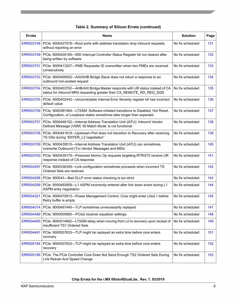
Table 2. Summary of Silicon Errata (continued)
Errata Name Solution Page
Chip Errata for the i.MX 6Solo/6DualLite, Rev. 7, 03/2019
NXP Semiconductors 9
ERR003748 PCIe: 9000427578—Root ports with address translation drop inbound requests, without reporting an error
No fix scheduled 131
ERR003749 PCIe: 9000426180—MSI Interrupt Controller Status Register bit not cleared after being written by software
No fix scheduled 132
ERR003751 PCIe: 9000413207—PME Requester ID overwritten when two PMEs are received consecutively
No fix scheduled 133
ERR003753 PCIe: 9000405932—AXI/AHB Bridge Slave does not return a response to an outbound non-posted request
No fix scheduled 134
ERR003754 PCIe: 9000403702—AHB/AXI Bridge Master responds with UR status instead of CA status for inbound MRd requesting greater than CX_REMOTE_RD_REQ_SIZE
No fix scheduled 135
ERR003755 PCIe: 9000402443—Uncorrectable Internal Error Severity register bit has incorrect default value
No fix scheduled 136
ERR003756 PCIe: 9000387484—LTSSM: Software-initiated transitions to Disabled, Hot Reset, Configuration, or Loopback states sometimes take longer than expected
No fix scheduled 137
ERR003757 PCIe: 9000448152—Internal Address Translation Unit (iATU): Inbound Vendor Defined Message (VDM) ‘ID Match Mode’ is not functional
No fix scheduled 138
ERR003758 PCIe: 9000441819—Upstream Port does not transition to Recovery after receiving TS OSs during “ENTER_L2 negotiation”
No fix scheduled 139
ERR003759 PCIe: 9000439510—Internal Address Translation Unit (iATU) can sometimes overwrite Outbound (Tx) Vendor Messages and MSIs
No fix scheduled 140
ERR003760 PCIe: 9000439175—Poisoned Atomic Op requests targeting RTRGT0 receive UR response instead of CA response
No fix scheduled 141
ERR004297 PCIe: 9000336356—Link configuration sometimes proceeds when incorrect TS Ordered Sets are received
No fix scheduled 142
ERR004298 PCIe: 900043—Bad DLLP error status checking is too strict No fix scheduled 143
ERR004299 PCIe: 9000493959—L1 ASPM incorrectly entered after link down event during L1 ASPM entry negotiation
No fix scheduled 144
ERR004321 PCIe: 9000470913—Power Management Control: Core might enter L0s/L1 before Retry buffer is empty
No fix scheduled 145
ERR004374 PCIe: 9000487440—TLP sometimes unnecessarily replayed No fix scheduled 147
ERR004489 PCIe: 9000505660—PCIe2 receiver equalizer settings No fix scheduled 148
ERR004490 PCIe: 9000514662—LTSSM delay when moving from L0 to recovery upon receipt of insufficient TS1 Ordered Sets
No fix scheduled 149
ERR004491 PCIe: 9000507633—TLP might be replayed an extra time before core enters recovery
No fix scheduled 151
ERR005184 PCIe: 9000507633—TLP might be replayed an extra time before core enters recovery
No fix scheduled 152
ERR005186 PCIe: The PCIe Controller Core Does Not Send Enough TS2 Ordered Sets During Link Retrain And Speed Change
No fix scheduled 153
Table 2. Summary of Silicon Errata (continued)
Errata Name Solution Page
Chip Errata for the i.MX 6Solo/6DualLite, Rev. 7, 03/2019
10 NXP Semiconductors
ERR005188 PCIe: The PCIe Controller cannot exit successfully L1 state of LTSSM when the Core Clock is removed
No fix scheduled 154
ERR005189 PCIe: PCIe Gen2/Gen3 Hardware Autonomous Speed Disable Bit In Configuration Register is not sticky
No fix scheduled 155
ERR005723 PCIe: PCIe does not support L2 power down No fix scheduled 156
ERR007554 PCIe: MSI Mask Register Reserved Bits not read-only No fix scheduled. 157
ERR007555 PCIe: iATU—Optional programmable CFG Shift feature for ECAM is not correctly updating address (9000642041)
No fix scheduled 158
ERR007556 PCIe: Core Delays Transition From L0 To Recovery After Receiving Two TS OS And Erroneous Data
No fix scheduled 159
ERR007557 PCIe: Extra FTS sent when Extended Synch bit is set No fix scheduled 160
ERR007559 PCIe: Core sends TS1 with non-PAD lane number too early in Configuration.Linkwidth.Accept State
No fix scheduled 161
ERR007573 PCIe: Link and lane number-match not checked in recovery No fix scheduled 162
ERR007575 PCIe: LTSSM delay when moving from L0 to recovery upon receipt of insufficient TS1 Ordered Sets
No fix scheduled 163
ERR007577 PCIe: DLLP/TLP can be missed on RX path when immediately followed by EIOS No fix scheduled 164
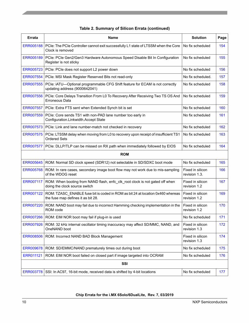
ROM
ERR005645 ROM: Normal SD clock speed (SDR12) not selectable in SD/SDXC boot mode No fix scheduled 165
ERR005768 ROM: In rare cases, secondary image boot flow may not work due to mis-sampling of the WDOG reset
Fixed in silicon revision 1.3.
166
ERR007117 ROM: When booting from NAND flash, enfc_clk_root clock is not gated off when doing the clock source switch
Fixed in silicon revision 1.2
167
ERR007122 ROM: TZASC_ENABLE fuse bit is coded in ROM as bit 24 at location 0x460 whereas the fuse map defines it as bit 28.
Fixed in silicon revision 1.2
169
ERR007220 ROM: NAND boot may fail due to incorrect Hamming checking implementation in the ROM code
Fixed in silicon revision 1.2
170
ERR007266 ROM: EIM NOR boot may fail if plug-in is used No fix scheduled 171
ERR007926 ROM: 32 kHz internal oscillator timing inaccuracy may affect SD/MMC, NAND, and OneNAND boot
Fixed in silicon revision 1.3
172
ERR008506 ROM: Incorrect NAND BAD Block Management Fixed in silicon revision 1.3
174
ERR009678 ROM: SD/EMMC/NAND prematurely times out during boot No fix scheduled 175
ERR011121 ROM: EIM NOR boot failed on closed part if image targeted into OCRAM No fix scheduled 176
SSI
ERR003778 SSI: In AC97, 16-bit mode, received data is shifted by 4-bit locations No fix scheduled 177
Table 2. Summary of Silicon Errata (continued)
Errata Name Solution Page
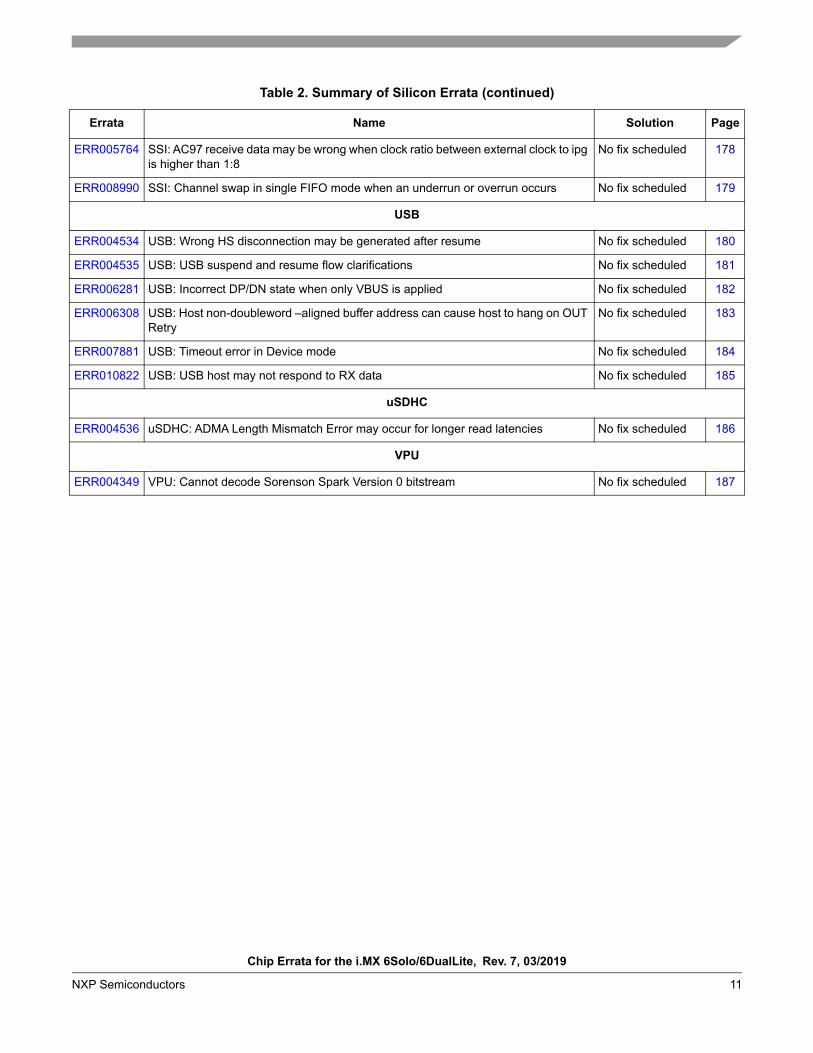
Chip Errata for the i.MX 6Solo/6DualLite, Rev. 7, 03/2019
NXP Semiconductors 11
ERR005764 SSI: AC97 receive data may be wrong when clock ratio between external clock to ipg is higher than 1:8
No fix scheduled 178
ERR008990 SSI: Channel swap in single FIFO mode when an underrun or overrun occurs No fix scheduled 179
USB
ERR004534 USB: Wrong HS disconnection may be generated after resume No fix scheduled 180
ERR004535 USB: USB suspend and resume flow clarifications No fix scheduled 181
ERR006281 USB: Incorrect DP/DN state when only VBUS is applied No fix scheduled 182
ERR006308 USB: Host non-doubleword –aligned buffer address can cause host to hang on OUT Retry
No fix scheduled 183
ERR007881 USB: Timeout error in Device mode No fix scheduled 184
ERR010822 USB: USB host may not respond to RX data No fix scheduled 185
uSDHC
ERR004536 uSDHC: ADMA Length Mismatch Error may occur for longer read latencies No fix scheduled 186
VPU
ERR004349 VPU: Cannot decode Sorenson Spark Version 0 bitstream No fix scheduled 187
Table 2. Summary of Silicon Errata (continued)
Errata Name Solution Page
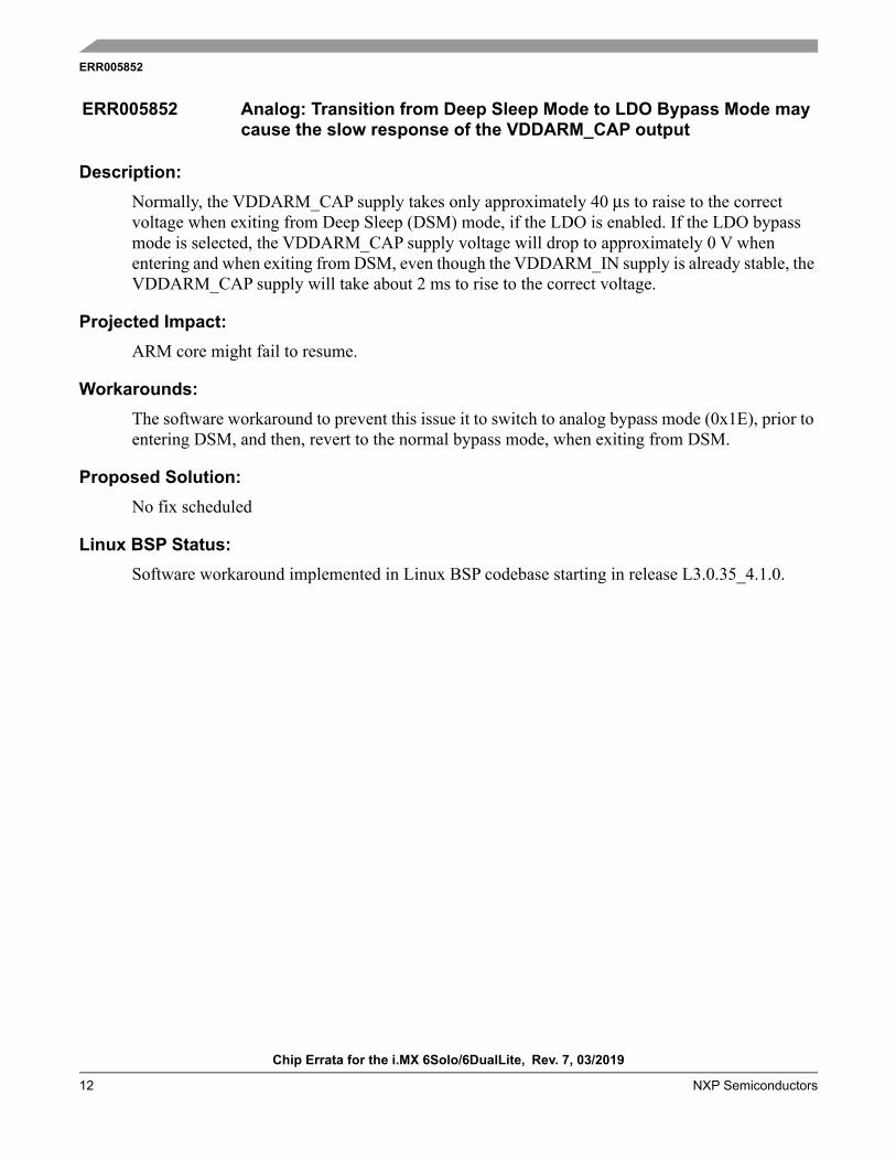
ERR005852
Chip Errata for the i.MX 6Solo/6DualLite, Rev. 7, 03/2019
12 NXP Semiconductors
Description:Normally, the VDDARM_CAP supply takes only approximately 40 μs to raise to the correct voltage when exiting from Deep Sleep (DSM) mode, if the LDO is enabled. If the LDO bypass mode is selected, the VDDARM_CAP supply voltage will drop to approximately 0 V when entering and when exiting from DSM, even though the VDDARM_IN supply is already stable, the VDDARM_CAP supply will take about 2 ms to rise to the correct voltage.
Projected Impact:ARM core might fail to resume.
Workarounds:The software workaround to prevent this issue it to switch to analog bypass mode (0x1E), prior to entering DSM, and then, revert to the normal bypass mode, when exiting from DSM.
Proposed Solution:No fix scheduled
Linux BSP Status:Software workaround implemented in Linux BSP codebase starting in release L3.0.35_4.1.0.
ERR005852 Analog: Transition from Deep Sleep Mode to LDO Bypass Mode may cause the slow response of the VDDARM_CAP output
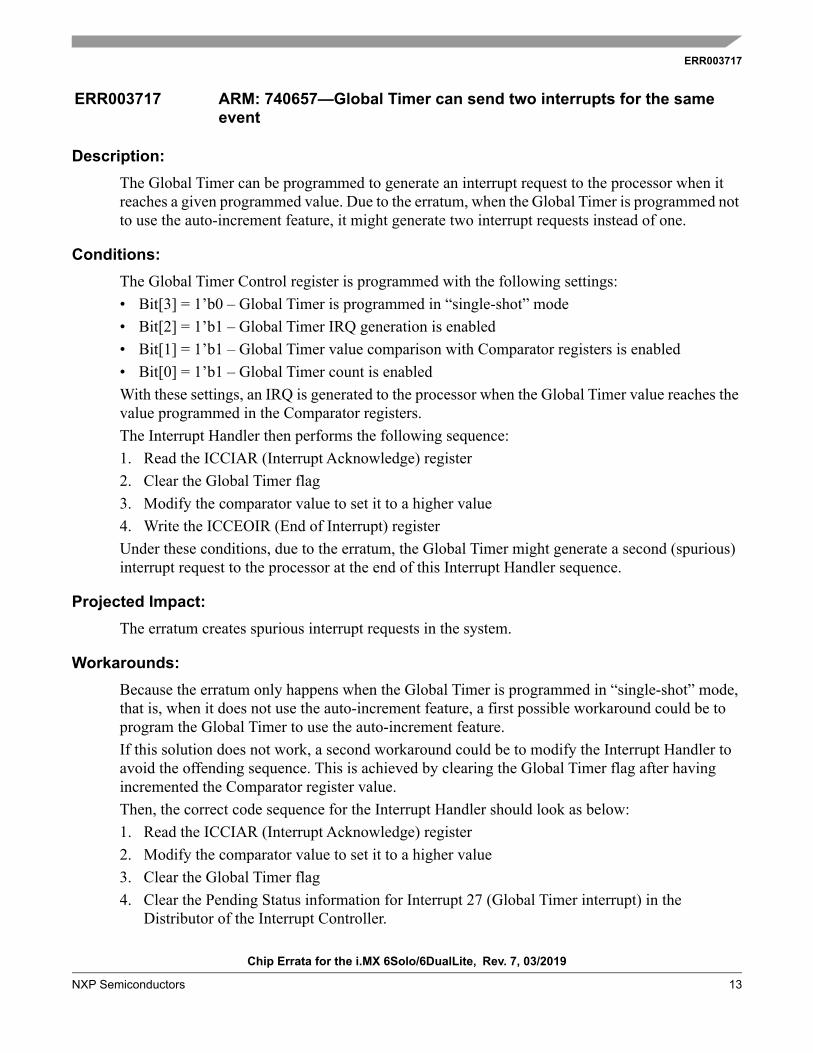
ERR003717
Chip Errata for the i.MX 6Solo/6DualLite, Rev. 7, 03/2019
NXP Semiconductors 13
Description:The Global Timer can be programmed to generate an interrupt request to the processor when it reaches a given programmed value. Due to the erratum, when the Global Timer is programmed not to use the auto-increment feature, it might generate two interrupt requests instead of one.
Conditions:The Global Timer Control register is programmed with the following settings:• Bit[3] = 1’b0 – Global Timer is programmed in “single-shot” mode• Bit[2] = 1’b1 – Global Timer IRQ generation is enabled• Bit[1] = 1’b1 – Global Timer value comparison with Comparator registers is enabled• Bit[0] = 1’b1 – Global Timer count is enabledWith these settings, an IRQ is generated to the processor when the Global Timer value reaches the value programmed in the Comparator registers. The Interrupt Handler then performs the following sequence:1. Read the ICCIAR (Interrupt Acknowledge) register2. Clear the Global Timer flag3. Modify the comparator value to set it to a higher value4. Write the ICCEOIR (End of Interrupt) registerUnder these conditions, due to the erratum, the Global Timer might generate a second (spurious) interrupt request to the processor at the end of this Interrupt Handler sequence.
Projected Impact:The erratum creates spurious interrupt requests in the system.
Workarounds:Because the erratum only happens when the Global Timer is programmed in “single-shot” mode, that is, when it does not use the auto-increment feature, a first possible workaround could be to program the Global Timer to use the auto-increment feature.If this solution does not work, a second workaround could be to modify the Interrupt Handler to avoid the offending sequence. This is achieved by clearing the Global Timer flag after having incremented the Comparator register value. Then, the correct code sequence for the Interrupt Handler should look as below:1. Read the ICCIAR (Interrupt Acknowledge) register2. Modify the comparator value to set it to a higher value3. Clear the Global Timer flag4. Clear the Pending Status information for Interrupt 27 (Global Timer interrupt) in the
Distributor of the Interrupt Controller.
ERR003717 ARM: 740657—Global Timer can send two interrupts for the same event
ERR003717
Chip Errata for the i.MX 6Solo/6DualLite, Rev. 7, 03/2019
14 NXP Semiconductors
5. Write the ICCEOIR (End of Interrupt) register
Proposed Solution:No fix scheduled
Linux BSP Status:Software workaround not implemented in the BSP. Functionality or mode of operation in which theerratum may manifest itself is not used. The BSP does not use ARM global timer. Theconfiguration and logic of the kernel does not make use of the Global Timer. If the Global timer isused, the workaround documented by ARM should be followed. Due to limitations of this timerspecifically in low power mode operation we do not recommend the use of this ARM Global timer.
ERR003718
Chip Errata for the i.MX 6Solo/6DualLite, Rev. 7, 03/2019
NXP Semiconductors 15
Description:Under very rare conditions, a faulty optimization in the Cortex®-A9 store buffer might lead to data corruption.
Conditions:The code sequence which exhibits the failure requires at least five cacheable writes in 64-bit data chunk:• Three of the writes must be in the same cache line• Another write must be in a different cache line• All of the above four writes hit in the L1 data cache• A fifth write is required in any of the above two cache lines that fully writes a 64-bit data chunkWith the above code sequence, under very rare circumstances, this fifth write might get corrupted, with the written data either being lost, or being written in another cache line.The conditions under which the erratum can occur are extremely rare, and require the coincidence of multiple events and states in the Cortex-A9 micro-architecture.As an example: let’s assume A, A’, A’’, and A’’’ are all in the same cache line—B and B’ are in another cache line. The following code sequence might trigger the erratum:
STR ASTR A’STR A’’STR BSTR A’’’ (or STR B’)
At the time where the first four STR are in the Cortex-A9 store buffer, and the fifth STR arrives at a very precise cycle in the Store Buffer input stage, then the fifth STR might not see its cache line dependency on the previous STR instructions. Because of this, in cases when the cache line A or B gets invalidated due to a coherent request from another CPU, the fifth STR might write in a faulty cache line, causing data corruption.An alternative version of the erratum might happen even without a coherent request — In the case when the fifth STR is a 64-bit write in the same location as one of A, A’, A’’, then the erratum might also be exhibited. Note that this is a quite uncommon scenario because it requires a first write to a memory location that is immediately and fully overwritten.
Projected Impact:When it occurs, this erratum creates a data corruption.
Workarounds:A software workaround is available for this erratum that requires setting bit[6] in the undocumented Diagnostic Control register, placed in CP15 c15 0 c0 1.The bit can be written in Secure state only, with the following Read/Modify/Write code sequence:
ERR003718 ARM: 743622—Faulty logic in the Store Buffer may lead to data corruption
ERR003718
Chip Errata for the i.MX 6Solo/6DualLite, Rev. 7, 03/2019
16 NXP Semiconductors
MRC p15,0,rt,c15,c0,1ORR rt,rt,#0x40MCR p15,0,rt,c15,c0,1
When this bit is set, the “fast lookup” optimization in the Store Buffer is disabled, which will prevent the failure to happen.Setting this bit has no visible impact on the overall performance or power consumption of the processor.
Proposed Solution:No fix scheduled
Linux BSP Status:Software workaround implemented in Linux BSP codebase (UBOOT) starting in releaseL3.0.35_4.1.0.
ERR003719
Chip Errata for the i.MX 6Solo/6DualLite, Rev. 7, 03/2019
NXP Semiconductors 17
Description:Overflow detection logic in the Performance Monitor Counters is faulty, and under certain timingconditions, the overflow may remain undetected. In this case, the Overflow Flag Status register(PMOVSR) is not updated as it should, and no interrupt is reported on the corresponding PMUIRQline.It is important to notice that the Cycle counter is not affected by this erratum.
Projected Impact:PMU overflow detection is not reliable.
Workarounds:The main workaround for this erratum is to poll the performance counter. The maximum incrementin a single cycle for a given event is 2. Therefore, polling can be infrequent as no counter canincrement by more than 2^32 in fewer than 2 billion cycles.If the main usage model for performance counters is collecting values over a long period, thenpolling can be used to collect values (and reset the counter) rather than waiting for an overflow tooccur. Polling can be done infrequently and overflow avoided.If the main usage model for performance counters relies on presetting the counter to some valueand waiting for an overflow to occur, then polling can be used to detect when an overflow eventhas been missed. An overflow can be determined to have been missed if the unsigned value in thecounter is less than the value preset into the counter. Again, polling can be done infrequentlybecause of the number of cycles it would need for this check to fail. In the case that the erratumwas triggered and an overflow event was missed, that counter sample can be thrown away or thetrue value can be reconstructed.An alternative workaround is to configure two counters to be triggered by the same event,staggering their initial count values by 1. This will result in the rollover being triggered by at leastcounter.This alternative workaround works for all Cortex-A9 events but the three following ones, due tothe fact these three events can increment by 2 in a single cycle:- 0x68 - Instructions coming out of the core renaming stage- 0x73 - Floating-point instructions- 0x74 - NEON instructionsFor these 3 events, only the first workaround is applicable to fix the defect.
Proposed Solution:No fix scheduled
ERR003719 ARM: 751469—Overflow in PMU counters may not be detected
ERR003719
Chip Errata for the i.MX 6Solo/6DualLite, Rev. 7, 03/2019
18 NXP Semiconductors
Linux BSP Status:Software workaround is not implemented because this erratum will not be encountered in normal device operation. The Linux BSP does not support this optional profiling feature. Users may add support for this profiling feature as required, but should ensure the multiple errata impacting theARM PMU are considered especially for multi-core usage.
ERR003720
Chip Errata for the i.MX 6Solo/6DualLite, Rev. 7, 03/2019
NXP Semiconductors 19
Description:In an MPCore configuration with two or more processors working in SMP mode with maintenance operation broadcast enabled, if a processor is interrupted while executing an ICIALLUIS operation, and performs another broadcast maintenance operation during its Interrupt Service Routine, then this second operation might not be executed on other processors in the cluster.
Conditions:The erratum requires an MPCore configuration with two or more CPUs working in SMP mode. One processor has interrupts enabled, and Cache and TLB maintenance broadcast enabled too (ACTLR.FW=1’b1). This processor executes an ICIALLUIS (invalidates all instruction caches Inner Shareable to Point of Unification). This instruction is executed on the processor, and also broadcast to other processors in the MPCore cluster. The processor then receives an interrupt (IRQ or FIQ), which interrupts the ICIALLUIS operation.During the Interrupt Service Routine, the processor executes any other Cache or TLB maintenance operation which is also broadcast to other processors in the MPCore cluster. If the other processors in the cluster receive this second maintenance operation before having completed the first ICIALLUIS operation, then the erratum occurs, as the other processors will not execute the second maintenance operation. This is because there is no “stacking” mechanism for acknowledge answers between the processors, so that the acknowledge request sent to signify the completion of the ICIALLUIS will be interpreted by the originating processor as an acknowledge for the second maintenance operation.
Projected Impact:Due to the erratum, the processor might end up with corrupted entries in the Cache or in the TLB, leading to possible failures in the system.
Workarounds:A software workaround is available for this erratum that involves setting bit[11] in the undocumented Diagnostic Control register, placed in CP15 c15 0 c0 1.This bit can be written in Secure state only, with the following Read/Modify/Write code sequence:
MRC p15,0,rt,c15,c0,1ORR rt,rt,#0x800MCR p15,0,rt,c15,c0,1
When it is set, this bit prevents CP15 maintenance operations to be interrupted.Using this software workaround is not expected to cause any visible impact on the system.
Proposed Solution:No fix scheduled
ERR003720 ARM/MP: 751472—An interrupted ICIALLUIS operation may prevent the completion of a following broadcast operation
ERR003720
Chip Errata for the i.MX 6Solo/6DualLite, Rev. 7, 03/2019
20 NXP Semiconductors
Linux BSP Status:Software workaround implemented in Linux BSP codebase (UBOOT) starting in release L3.0.35_4.1.0.
ERR003721
Chip Errata for the i.MX 6Solo/6DualLite, Rev. 7, 03/2019
NXP Semiconductors 21
Description:Under very rare timing circumstances, the automatic Data prefetcher might cause address hazard issues, possibly leading to a data corruption or a deadlock of the processor.
Conditions:The erratum can only happen when the Data Cache and MMU are enabled in the following cases:• On all memory regions marked as Write-Back Non-Shared, when the Data Prefetcher in L1 is
enabled (ACTLR[2]=1’b1), regardless of the ACTLR.SMP bit.• On all memory regions marked as Write-Back Shared, when the Data Prefetch Hint in L2 is
enabled (ACTLR[1]=1’b1), and when the processor is in SMP mode (ACTLR.SMP=1’b1).
Projected Impact:When the bug happens, a data corruption or a processor deadlock can happen.
Workarounds:The workaround for this erratum requires not enabling the automatic Data Prefetcher by keeping ACTRL[2:1]=2’b00, which is the default value on exit from reset.Although this feature might show significant performance gain on a few synthetic benchmarks, it usually has no impact on real systems. It means, this workaround is not expected to cause any visible impact on final products.
Proposed Solution:No fix scheduled
Linux BSP Status:Software workaround not implemented in the BSP. Functionality or mode of operation in which theerratum may manifest itself is not used. Linux BSP keeps ACTRL[2:1]=2’b00.
ERR003721 ARM: 751473—Under very rare circumstances, Automatic Data prefetcher can lead to deadlock or data corruption
ERR003723
Chip Errata for the i.MX 6Solo/6DualLite, Rev. 7, 03/2019
22 NXP Semiconductors
Description:Under rare conditions, a watchpoint on the second part of an unaligned access that crosses a 4 KB page boundary and that is missed in the micro-TLB for the second part of its request might be undetected.The erratum requires a previous conditional instruction that accesses the second 4 KB memory region (= where the watchpoint is set), is missed in the micro-TLB, and is condition failed. The erratum also requires that no other micro-TLB miss occurs between this conditional failed instruction and the unaligned access. This implies that the unaligned access must hit in the micro-TLB for the first part of its request.
Projected Impact:A valid watchpoint trigger is missed.
Workarounds:In case, a watchpoint is set on any of the first 3 bytes of a 4 KB memory region, and unaligned accesses are not being faulted, then the erratum might happen.The workaround then requires setting a guard watchpoint on the last byte of the previous page, and dealing with any “false positive” matches as and when they occur.
Proposed Solution:No fix scheduled
Linux BSP Status:A software workaround is not implemented because this erratum will not be encountered in normal device operation. The Linux BSP does not use this debug feature—the ARM workaround should be followed.
ERR003723 ARM: 751476—May miss a watchpoint on the second part of an unaligned access that crosses a page boundary
ERR003724
Chip Errata for the i.MX 6Solo/6DualLite, Rev. 7, 03/2019
NXP Semiconductors 23
Description:A microTLB entry might be corrupted following an ASID switch, possibly corrupting subsequentMMU translations.The erratum requires execution of an explicit memory access, which might be speculative. Thismemory access misses in the TLB and cause a translation table walk. The erratum occurs when thetranslation table walk starts before the ASID switch code sequence, but completes after the ASIDswitch code sequence. In this case, a new entry is allocated in the microTLB for the TLB entry forthis translation table walk, but corresponding to the old ASID. Because the microTLB does notrecord the ASID value, the new MMU translation, which should happen with the new ASIDfollowing the ASID switch, might hit this stale microTLB entry and become corrupted.Note that there is no Trustzone Security risk because the Security state of the access is held in themicroTLB, and cannot be corrupted.
Projected Impact:The errata might cause MMU translation corruptions.
Workarounds:The workaround for this erratum involves adding a DSB in the ASID switch code sequence. The ARM architecture only mandates ISB before and after the ASID switch. Adding a DSB prior to the ASID switch ensures that the Page Table Walk completes prior to the ASID change, so that no stale entry can be allocated in the micro-TLB.The examples in the ARM Architecture Reference Manual for synchronizing the change in the ASID and TTBR need to be changed as follows:The sequence:
Change ASID to 0ISBChange Translation Table Base RegisterISBChange ASID to new value
becomesDSBChange ASID to 0ISBChange Translation Table Base RegisterISBDSBChange ASID to new value
the sequence:Change Translation Table Base Register to the global-only mappings
ERR003724 ARM: 754322—Possible faulty MMU translations following an ASID switch
ERR003724
Chip Errata for the i.MX 6Solo/6DualLite, Rev. 7, 03/2019
24 NXP Semiconductors
ISBChange ASID to new valueISBChange Translation Table Base Register to new value
becomesChange Translation Table Base Register to the global-only mappingsISBDSBChange ASID to new valueISBChange Translation Table Base Register to new value
and the sequence:Set TTBCR.PD0 = 1ISBChange ASID to new valueChange Translation Table Base Register to new valueISBSet TTBCR.PD0 = 0
becomesSet TTBCR.PD0 = 1ISBDSBChange ASID to new valueChange Translation Table Base Register to new valueISBSet TTBCR.PD0 = 0
Proposed Solution:No fix scheduled
Linux BSP Status:Software workaround implemented in Linux BSP codebase starting in release L3.0.35_4.1.0.
ERR003725
Chip Errata for the i.MX 6Solo/6DualLite, Rev. 7, 03/2019
NXP Semiconductors 25
Description:The ISB is implemented as a branch in the Cortex-A9 micro-architecture. This implies that events 0x0C (software change of PC) and 0x0D (immediate branch) are asserted when an ISB occurs. This is not compliant with the ARM architecture.
Projected Impact:The count of events 0x0C and 0x0D are not 100% precise when using the Performance Monitor counters, due to the ISB being counted in addition to the real software changes to PC (for 0x0C) and immediate branches (0x0D).The erratum also causes the corresponding PMUEVENT bits to toggle in case an ISB is executed.• PMUEVENT[13] relates to event 0x0C• PMUEVENT[14] relates to event 0x0D
Workarounds:Count ISB instructions along with event 0x90. The user should subtract this ISB count from the results obtained in events 0x0C and 0x0D, to obtain the precise count of software change of PC (0x0C) and immediate branches (0x0D).
Proposed Solution:No fix scheduled
Linux BSP Status:Software workaround is not implemented because this erratum will not be encountered in normal device operation.The Linux BSP does not support this optional profiling feature. Users may addsupport for this profiling feature as required, but should ensure the multiple errata impacting theARM PMU are considered especially for multi-core usage.
ERR003725 ARM: 725631—ISB is counted in Performance Monitor events 0x0C and 0x0D
ERR003726
Chip Errata for the i.MX 6Solo/6DualLite, Rev. 7, 03/2019
26 NXP Semiconductors
Description:The ARM Debug Architecture specifies registers 838 and 839 as “Alias of the MainID register”. They should be accessible through the APB Debug interface at addresses 0xD18 and 0xD1C.In Cortex-A9, the two alias addresses are not implemented. A read access at any of these two addresses returns 0, instead of the MIDR value.Note that read accesses to these two registers through the internal CP14 interface are trapped to UNDEF, which is compliant with the ARM Debug architecture. So, the erratum only applies to the alias addresses through the external Debug APB interface.
Projected Impact:If the debugger or any other external agent tries to read the MIDR register using the alias addresses, it will get a faulty answer (0x0), which can cause all sorts of malfunction in the debugger afterwards.
Workarounds:The workaround for this erratum requires always accessing the MIDR at its original address, 0xD00, and not at any of its alias addresses.
Proposed Solution:No fix scheduled
Linux BSP Status:Software workaround is not implemented because this erratum will not be encountered in normal device operation.
ERR003726 ARM: 729817—MainID register alias addresses are not mapped on Debug APB interface
ERR003727
Chip Errata for the i.MX 6Solo/6DualLite, Rev. 7, 03/2019
NXP Semiconductors 27
Description:When the processor is in debug state, an instruction written to the ITR after a Load/Store instruction that aborts gets executed on clearing the SDABORT_l, instead of being discarded.
Projected Impact:Different failures can happen due to the instruction being executed when it should not. In most cases, it is expected that the failure will not cause any significant problem.
Workarounds:There are a selection of workarounds with increasing complexity and decreasing impact. In each case, the impact is a loss of performance when debugging:• Do not use stall mode• Do not use stall mode when doing load/store operations• Always check for a sticky abort after issuing a load/store operation in stall mode (the cost of this
probably means the above second workaround is a preferred alternative)• Always check for a sticky abort after issuing a load/store operation in stall mode, before issuing
any further instructions that might corrupt important target state (such as, further load/store instructions, instructions that write to “live” registers [VFP, CP15, etc.])
Proposed Solution:No fix scheduled
Linux BSP Status:Software workaround is not implemented because this erratum will not be encountered in normal device operation.
ERR003727 ARM: 729818—In debug state, next instruction is stalled when sdabort flag is set, instead of being discarded
ERR003728
Chip Errata for the i.MX 6Solo/6DualLite, Rev. 7, 03/2019
28 NXP Semiconductors
Description:Event 0x74 counts the total number of Neon instructions passing through the register rename pipeline stage. Due to the erratum, the “stall” information is not taken into account. So, one Neon instruction that remains for n cycles in the register rename stage is counted as n Neon instructions. As a consequence, the count of event 0x74 might be corrupted, and cannot be relied upon. The event is also reported externally on PMUEVENT[38:37], which suffers from the same inaccuracy.
Projected Impact:The implication of this erratum is that Neon instructions cannot be counted reliably in the versions of the product that are affected by this erratum.
Workarounds:No workaround is possible to achieve the required functionality of counting how many Neon instructions are executed (or renamed) in the processor.
Proposed Solution:No fix scheduled
Linux BSP Status:Software workaround is not implemented because this erratum will not be encountered in normal device operation. The Linux BSP does not support this optional profiling feature. Users may addsupport for this profiling feature as required, but should ensure the multiple errata impacting theARM PMU (Performance Monitoring Unit) are considered especially for multi-core usage.
ERR003728 ARM: 740661—Event 0x74 / PMUEVENT[38:37] may be inaccurate
ERR003729
Chip Errata for the i.MX 6Solo/6DualLite, Rev. 7, 03/2019
NXP Semiconductors 29
Description:Event 0x68 counts the total number of instructions passing through the register rename pipeline stage. Under certain conditions, some branch-related instructions might pass through this pipeline stage without being counted. As a consequence, event 0x68 might be inaccurate, lower than expected. The event is also reported externally on PMUEVENT[9:8], which suffers from the same inaccuracy.
Conditions:The erratum occurs when the following conditions are met:• Events are enabled• One of the PMU counters is programmed to count event 0x68 — number of instructions passing
through the register rename stage. Alternatively, an external component counts, or relies on, PMUEVENT[9:8].
• A program, containing the following instructions, is executed:— A Branch immediate, without Link— An ISB instruction— An HB instruction, without Link and without parameter, in Thumb2EE state— An ENTERX or LEAVEX instruction, in Thumb2 or Thumb2EE state
• The program executed is causing some stalls in the processor pipelineUnder certain timing conditions specific to the Cortex-A9 micro-architecture, a cycle stall in the processor pipeline might “hide” the instructions mentioned above, thus ending with a corrupted count for event 0x68, or a corrupted value on PMUEVENT[9:8] during this given cycle. If the “hidden” instruction appears in a loop, the count difference can be significant.As an example, let’s consider the following loop:
loop mcr 15, 0, r2, cr9, cr12, {4}adds r3, #1cmp.w r3, #loop_numberbne.n loop
The loop contains four instructions; so, the final instruction count should (approximately) be four times the number of executed loops. In practice, the MCR is causing a pipeline stall that “hides” the branch instruction (bne.n); so, only three instructions are counted per loop, and the final count appears as three times the number of executed loops.
Projected Impact:The implication of this erratum is that the values of event 0x68 and PMUEVENT[9:8] are imprecise, and cannot be relied upon.
Workarounds:No workaround is possible to achieve the required functionality of counting how many instructions are precisely passing through the register rename pipeline stage.
ERR003729 ARM: 740663—Event 0x68 / PMUEVENT[9:8] may be inaccurate
ERR003729
Chip Errata for the i.MX 6Solo/6DualLite, Rev. 7, 03/2019
30 NXP Semiconductors
Proposed Solution:No fix scheduled
Linux BSP Status:Software workaround is not implemented because this erratum will never be encountered in normaldevice operation.The Linux BSP does not support this optional profiling feature. Users may add support for this profiling feature as required, but should ensure the multiple errata impacting the ARM PMU (Performance Monitoring Unit) are considered especially for multi-core usage.
ERR003730
Chip Errata for the i.MX 6Solo/6DualLite, Rev. 7, 03/2019
NXP Semiconductors 31
Description:Under very rare circumstances, a deadlock can happen in the processor when it is handling a minimum of seven PLD instructions, shortly followed by one LDM to an uncacheable memory location.The LDM is treated as uncacheable in the following cases:• The LDM is performed while the Data Cache is OFF• The LDM is targeting a memory region marked as Strongly Ordered, Device, Normal Memory
Non-Cacheable, or Normal Memory Write-Through• The LDM is targeting a memory region marked as Shareable Normal Memory Write-Back, and
the CPU is in AMP mode.
Conditions:The code sequence that exhibits this erratum requires at least seven PLDs, shortly followed by one LDM, to an uncacheable memory region. The erratum happens when the LDM appears on the AXI bus before any of the seven PLDs. This can possibly happen if the first PLD is a miss in the micro-TLB; in that case, it needs to perform a TLB request which might not be serviced immediately because the mainTLB is already performing a Page Table Walk for another resource (for example, instruction side), or because the PLD request itself to the mainTLB is missing and causing a Page Table Walk.Also note that the above conditions are not sufficient to recreate the failure, as additional rare conditions on the internal state of the processor are necessary to exhibit the errata.
Projected Impact:The erratum might create a processor deadlock. However, the conditions that are required for this to occur are extremely unlikely to occur in real code sequences.
Workarounds:The primary workaround might be to avoid the offending code sequence, that is, not to use uncacheable LDM when making intensive use of PLD instructions.In case the above workaround cannot be done, another workaround for this erratum can be to set bit[20] in the undocumented Control register, which is placed in CP15 c15 0 c0 1.This bit needs to be written with the following Read/Modify/Write code sequence:
MRC p15,0,r0,c15,c0,1ORR r0,r0,#0x00100000MCR p15,0,r0,c15,c0,1
Setting this bit causes all PLD instructions to be treated as NOPs, with the consequence that code sequences usually using the PLDs, such as the memcpy() routine, might suffer from a visible performance drop.
ERR003730 ARM: 743623—Bad interaction between a minimum of seven PLDs and one Non-Cacheable LDM can lead to a deadlock
ERR003730
Chip Errata for the i.MX 6Solo/6DualLite, Rev. 7, 03/2019
32 NXP Semiconductors
Proposed Solution:No fix scheduled
Linux BSP Status:Software workaround not implemented in the BSP. Functionality or mode of operation in which theerratum may manifest itself is not used. Users should check their custom OS and either avoid the code sequence or apply the ARM recommended workaround. The ARM recommended workaround does have a performance impact.
ERR003731
Chip Errata for the i.MX 6Solo/6DualLite, Rev. 7, 03/2019
NXP Semiconductors 33
Description:An imprecise external abort received while the processor is ready to enter into WFI state might cause a processor deadlock.Explicit memory transactions can be completed by inserting a DSB before the WFI instruction. However, this does not prevent memory accesses generated by previously issued PLD instructions page table walks associated with previously issued PLD instructions or as a result of the PLE engine.If an external abort is returned as a result of one of these memory accesses after executing a WFI instruction, the processor can cause a deadlock.
Projected Impact:In case, the non-explicit memory request receives an external imprecise abort response while the processor is ready to enter into WFI state, the processor might cause a deadlock.In practical systems, it is not expected that these memory transactions will generate an external abort, as external aborts are usually a sign of significant corruption in the system.
Workarounds:A possible workaround for this erratum is to protect all memory regions that can return an imprecise external abort with the correct MMU settings, to prevent any external aborts.
Proposed Solution:No fix scheduled
Linux BSP Status:The BSP uses correct MMU settings and does not present conditions that can cause an impreciseexternal abort. BSP has exception handlers for such aborts.
ERR003731 ARM: 743626—An imprecise external abort, received while the processor enters WFI, may cause a processor deadlock
ERR003732
Chip Errata for the i.MX 6Solo/6DualLite, Rev. 7, 03/2019
34 NXP Semiconductors
Description:About the DBGPCSR register, the ARM architecture specifies that:• DBGPCSR[31:2] contains sampled value of bits [31:2] of the PC.
The sampled value is an instruction address plus an offset that depends on the processor instruction set state.
• DBGPCSR[1:0] contains the meaning of PC sample value, with the following permitted values:— 0b00 ((DBGPCSR[31:2] << 2) - 8) references an ARM state instruction— 0bx1 ((DBGPCSR[31:1] << 1) - 4) references a Thumb or ThumbEE state instruction— 0b10 IMPLEMENTATION DEFINED
This field encodes the processor instruction set state, so that the profiling tool can calculate the true instruction address by subtracting the appropriate offset from the value sampled in bits [31:2] of the register.In Cortex-A9, the DBGPCSR samples the target address of executed branches (but possibly still speculative to data aborts), with the following encodings:• DBGPCSR[31:2] contains the address of the target branch instruction, with no offset• DBGPCSR[1:0] contains the execution state of the target branch instruction:
— 0xb00 for an ARM state instruction— 0xb01 for a Thumb2 state instruction— 0xb10 for a Jazelle state instruction— 0xb11 for a Thumb2EE state instruction
Projected Impact:The implication of this erratum is that the debugger tools neither rely on the architected description for the value of DBGPCSR[1:0], nor remove any offset from DBGPCSR[31:2], to obtain the expected PC value.Subtracting 4 or 8 to the DBGPCSR[31:2] value would lead to an area of code that is unlikely to have been recently executed, or that could even not contain any executable code.The same might be true for Thumb instructions at half-word boundaries, in which case PC[1]=1 but DBGPCSR[1]=0, or ThumbEE instructions at word boundaries, with PC[1]=0 and DBGPCSR[1]=1.In Cortex-A9, because the DBGPCSR is always a branch target (= start of a basic block to the tool), the debugger should be able to spot many of these cases and attribute the sample to the right basic block.
Workarounds:The debugger tools can find the expected PC value and instruction state by reading the DBGPCSR register, and consider it as described in the Description section.
ERR003732 ARM: 751471—DBGPCSR format is incorrect
ERR003732
Chip Errata for the i.MX 6Solo/6DualLite, Rev. 7, 03/2019
NXP Semiconductors 35
Proposed Solution:No fix scheduled
Linux BSP Status:Software workaround is not implemented because this erratum will never be encountered in normaldevice operation. Software workaround not applicable to the BSP since it is a debug feature. Usersshould use the ARM recommended workaround if using this debug feature in their application.
ERR003733
Chip Errata for the i.MX 6Solo/6DualLite, Rev. 7, 03/2019
36 NXP Semiconductors
Description:A conditional LDREX might set the internal exclusive monitor of the Cortex-A9 even when its condition fails. So, any subsequent STREX that depends on this LDREXcc might succeed when it should not.
Projected Impact:The implication of the erratum is that a subsequent STREX might succeed when it should not. So, the memory region protected by the exclusive mechanism can be corrupted if another agent is accessing it at the same time.
Workarounds:The workaround for this erratum can be not to use conditional LDREX along with non-conditional STREX.• If no conditional LDREX is used, the erratum cannot be triggered.• If conditional LDREX is used, the associated STREX should be conditional too with the same
condition, so that even if the exclusive monitor is set by the condition failed LDREX, the following STREX will not be executed because it will be condition failed too. For most situations this will naturally be the case anyway.
Proposed Solution:No fix scheduled
Linux BSP Status:Software workaround not implemented in the BSP. Functionality or mode of operation in which the erratum may manifest itself is not used.The BSP does not use conditional LDREX.
ERR003733 ARM: 751480—Conditional failed LDREXcc can set the exclusive monitor
ERR003734
Chip Errata for the i.MX 6Solo/6DualLite, Rev. 7, 03/2019
NXP Semiconductors 37
Description:When two outstanding read memory requests to device or non-cacheable normal memory regions are issued by the Cortex-A9, and the first one receives an imprecise external abort, then the second access might falsely report an imprecise external abort.
Conditions:The erratum can only happen in systems which can generate imprecise external aborts on device or non-cacheable normal memory regions accesses.
Projected Impact:When the erratum occurs, a second, spurious imprecise abort might be reported to the core when it should not.In practice, the failure is not expected to cause any significant issues to the system because imprecise aborts are usually unrecoverable failures. Because the spurious abort can only happen following a first imprecise abort—either the first abort is ignored and the spurious abort is then ignored too, or it is acknowledged and probably generates a critical failure in the system.
Workarounds:There is no practical software workaround for the failure.
Proposed Solution:No fix scheduled
Linux BSP Status:Software workaround cannot be implemented to mask or workaround this SoC issue. This erratumwill result in impacted or reduced functionality as described above. Users should evaluate their specific use case and apply the recommended workaround to prevent the occurrence of this erratum. Please contact your support channel if you have any questions or concerns.
ERR003734 ARM: 752519—An imprecise abort may be reported twice on non-cacheable reads
ERR003735
Chip Errata for the i.MX 6Solo/6DualLite, Rev. 7, 03/2019
38 NXP Semiconductors
Description:The Cortex-A9 implements a small counter that ensures the external visibility of all stores in a finite amount of time, causing an eventual drain of the merging store buffer. This is to avoid an earlier issue, where written data could potentially remain indefinitely in the Store Buffer.This store buffer has merging capabilities, and will continue merging data as long as the write accesses are performed in the same cache line. The issue that causes this erratum is that the draining counter is reset each time a new data merging is performed.When a code sequence is looping, and keeps on writing data in the same cache line, then the external visibility of the written data might not be ensured.A livelock situation might consequently occur in case any external agent is relying on the visibility of the written data, and that the writing processor cannot be interrupted while doing its writing loop.
Conditions:The erratum can only happen on normal memory regions.Two example scenario, which might trigger the erratum, are described below:• The processor keeps on incrementing a counter: writing the same word at the same address. The
external agent (possibly another processor) is polling on this address, waiting for any update of the counter value to proceed.The store buffer will keep on merging the updated value of the counter in its cache line, so that the external agent will never see any updated value, possibly leading to livelock.
• The processor writes a value in a given word to indicate completion of its task, then keeps on writing data in an adjacent word in the same cache line.The external agent keeps on polling the first word memory location to check when the processor has completed its task. The situation is the same as above, as the cache line might remain indefinitely in the merging store buffer, creating a possible livelock in the system.
Projected Impact:This erratum might create performance issues, or worst case livelock scenario, in case the external agent relies on the automatic visibility of the written data in a finite amount of time.
Workarounds:The recommended workaround for this erratum involves inserting a DMB operation after the faulty write operation in code sequences that might be affected by this erratum. This ensures visibility of the written data by any external agent.
Proposed Solution:No fix scheduled
ERR003735 ARM: 754323—Repeated Store in the same cache line may delay the visibility of the Store
ERR003735
Chip Errata for the i.MX 6Solo/6DualLite, Rev. 7, 03/2019
NXP Semiconductors 39
Linux BSP Status:Software workaround is not implemented because this erratum will not be encountered in normal device operation. However, the ARM Linux kernel common code has added the necessary DMB in places to ensure the visibility of the written data to any external agent.The workaround for this erratum is to insert a DMB operation after the faulty write operation in code sequences that this erratum might affect, to ensure the visibility of the written data to any external agent. The BSP does use DMBs however the specific condition or scenario is not seen in kernel code.
ERR003736
Chip Errata for the i.MX 6Solo/6DualLite, Rev. 7, 03/2019
40 NXP Semiconductors
Description:The Sticky Pipeline Advance bit is bit[25] of the DBGDSCR register. This bit enables the debugger to detect whether the processor is idle. This bit is set to 1 every time the processor pipeline retires one instruction.A write to DBGDRCR[3] clears this bit.The erratum is that the Cortex-A9 does not implement any debug APB access to DBGDRCR[3].
Projected Impact:Due to the erratum, the Sticky Pipeline Advance bit in the DBGDSCR cannot be cleared by the external debugger. In practice, this makes the Sticky Pipeline Advance bit concept unusable on Cortex-A9 processors.
Workarounds:There is no practical workaround for this erratum. The only possible way to reset the Sticky Pipeline Advance bit is to assert the nDBGRESET input pin on the processor. This obviously has the side effect to reset all debug resources in the concerned processor, and any other additional Coresight components nDBGRESET is connected to.
Proposed Solution:No fix scheduled
Linux BSP Status:Software workaround is not implemented because this erratum will never be encountered in normaldevice operation.
ERR003736 ARM: 756421—Sticky Pipeline Advance bit cannot be cleared from debug APB accesses
ERR003737
Chip Errata for the i.MX 6Solo/6DualLite, Rev. 7, 03/2019
NXP Semiconductors 41
Description:The ARM architecture specifies that ARM opcodes of the form 11110 100x001 xxxx xxxx xxxx xxxx xxxx are “Unallocated memory hint (treat as NOP)” if the core supports the MP extensions, as the Cortex-A9 does.The errata is that the Cortex-A9 generates an UNDEFINED exception when bits [15:12] of the instruction encoding are different from 4’b1111, instead of treating the instruction as a NOP.
Projected Impact:Due to the erratum, an unexpected UNDEFINED exception might be generated. In practice, this erratum is not expected to cause any significant issue, as such instruction encodings are not supposed to be generated by any compiler, nor used by any handcrafted program.
Workarounds:A possible workaround for this erratum is to modify the instruction encoding with bits[15:12]=4.b1111, so that the instruction is truly treated as a NOP by the Cortex-A9.If the instruction encoding cannot be modified, the UNDEFINED exception handler has to cope with this case, and emulate the expected behavior of the instruction, that is, do nothing (NOP), before returning to normal program execution.
Proposed Solution:No fix scheduled
Linux BSP Status:Software workaround not implemented in Linux BSP. Functionality or mode of operation in whichthe erratum may manifest itself is not used. Software workaround not applicable to the BSP asinstruction encodings are not generated by compiler.
ERR003737 ARM: 757119—Some “Unallocated memory hint” instructions generate an UNDEFINED exception instead of being treated as NOP
ERR003738
Chip Errata for the i.MX 6Solo/6DualLite, Rev. 7, 03/2019
42 NXP Semiconductors
Description:In the Data Cache, parity error detection is faulty. Parity error might not be detected when the line exits from the Data Cache, due to a line replacement, or due to a coherent request from another processor or from the ACP, or because of a CP15 cache clean operation.
Projected Impact:Due to the erratum, a corrupted line might be evicted or transferred from the processor without the parity error being detected and reported.
Workarounds:There is no workaround for this erratum.
Proposed Solution:No fix scheduled
Linux BSP Status:Software workaround not implemented in Linux BSP. Functionality or mode of operation in which the erratum may manifest itself is not used. Parity is not supported on i.MX 6 series. See erratumERR005187 regarding the BSP interaction with the parity interrupt.
ERR003738 ARM: 751475—Parity error may not be reported on full cache line access (eviction / coherent data transfer / cp15 clean operations)
ERR003739
Chip Errata for the i.MX 6Solo/6DualLite, Rev. 7, 03/2019
NXP Semiconductors 43
Description:Data linefills are returned as 4-beat bursts of 64-bit data on the AXI bus. When the first three beat of data are valid, and the fourth one aborts, then the abort is not detected by the processor logic and no abort exception is taken. The processor then behaves as if no abort is reported on the line. It can allocate the line in its Data Cache, and use the aborted data during its program flow.
Conditions:The processor needs to work with Data Cache enabled, and access some cacheable memory regions (Write Back, either Shared or Non-Shared).The memory system underneath the processor needs to be able to generate aborts in this memory region, and must be able to generate aborts with a granularity smaller than the cache line.
Projected Impact:When the erratum triggers, the processor does not detect the abort, so it might use some invalid (aborted) data without entering the Data Abort exception handler as it should normally do.
Workarounds:None
Proposed Solution:No fix scheduled
Linux BSP Status:A software workaround is possible but it hasn’t been implemented in the Linux BSP yet. BSP functionality may be affected in some configurations and use cases as described above. Users should evaluate their specific use case and apply the recommended workaround to prevent the occurrence of this erratum. Please contact your support channel if you have any questions or concerns.
ERR003739 ARM: 751470—Imprecise abort on the last data of a cache linefill may not be detected
ERR003741
Chip Errata for the i.MX 6Solo/6DualLite, Rev. 7, 03/2019
44 NXP Semiconductors
Description:The “High Priority for SO and Dev reads” feature can be enabled by setting the bit[10] of the PL310 Auxiliary Control Register to 1. When enabled, it gives priority to Strongly Ordered and Device reads over cacheable reads in the PL310 AXI master interfaces. When PL310 receives a continuous flow of SO or Device reads, this can prevent cacheable reads, which are misses in the L2 cache, from being issued to the L3 memory system.
Conditions:The erratum occurs when the following conditions are met:• The bit[10] “High Priority for SO and Dev reads enable” of the PL310 Auxiliary Control
Register is set to 1• PL310 receives a cacheable read that is a miss in the L2 cache• PL310 receives a continuous flow of SO or Device reads that take all address slots in the master
interface
Projected Impact:When the above conditions are met, the linefill resulting from the L2 cache miss is not issued till the flow of SO/Device reads stops. Note that each PL310 master interface has four address slots, so that the Quality of Service issue only appears on the cacheable read, if the L1 is able to issue at least four outstanding SO/Device reads.
Workarounds:A workaround is only necessary in systems that are able to issue a continuous flow of SO or Device reads. In such a case, the workaround is to disable the “High Priority for SO and Dev reads” feature. This is the behavior by default.
Proposed Solution:No fix scheduled
Linux BSP Status:Software workaround not implemented in Linux BSP. Functionality or mode of operation in whichthe erratum may manifest itself is not used. The bit[10] “High Priority for SO and Dev readsenable” of the PL310 Auxiliary Control Register is not enabled in the BSP.
ERR003741 ARM/PL310: 729815—The “High Priority for SO and Dev reads” feature can cause Quality of Service issues to cacheable read transactions
ERR003743
Chip Errata for the i.MX 6Solo/6DualLite, Rev. 7, 03/2019
NXP Semiconductors 45
Description:In the ARM L2 cache controller, PL310, hazard checking is done on bits [31:5] of the address.When a read with Normal Memory (cacheable or not) attributes is received by PL310, hazard checking is performed with the active writes of the store buffer. If an address matching is detected, the read is stalled till the write completes.Due to this erratum, a continuous flow of writes can stall a read targeting the same memory area.
Conditions:The erratum occurs when the following conditions are met:• PL310 receives a continuous write traffic targeting the same address marked with Normal
Memory attributes• While treating this flow, PL310 receives a read targeting the same 32-byte memory area
Projected Impact:When the conditions above are met, the read might be stalled till the write flow stops.Note that this erratum does not lead to any data corruption.Note also that normal software code is not expected to contain long write sequence like the one causing this erratum to occur.
Workarounds:There is no workaround for this erratum. A workaround is not expected to be necessary for this erratum either.
Proposed Solution:No fix scheduled
Linux BSP Status:Software workaround not implemented in Linux BSP. Functionality or mode of operation in whichthe erratum may manifest itself is not used.
ERR003743 ARM/PL310: 754670—A continuous write flow can stall a read targeting the same memory area
ERR004324
Chip Errata for the i.MX 6Solo/6DualLite, Rev. 7, 03/2019
46 NXP Semiconductors
Description:The ARM architecture, and general rules of coherency, requires reads to the same memory location to be observed in order.Due to some internal replay path mechanisms, the Cortex-A9 can see a read access bypassed by a following read access to the same memory location, thus not observing the values in program order.
Conditions:It can only happen on memory regions marked as Normal Memory Write-Back Shared.
Projected Impact:The erratum leads to data coherency failure.
Workarounds:The vast majority of multi-processing code is not written in a style which exposes the erratum. So, the erratum is expected to affect very specific areas of code which rely on this read ordering behavior.A first workaround for this erratum consists in using LDREX instead of standard LDR in volatile memory places where a strict read ordering is required.An alternative solution consists in inserting a DMB between the affected LDR which requires this strict ordering rule. This is the recommended workaround for tool chains integration.
Proposed Solution:No fix scheduled
Linux BSP Status:Software workaround is not implemented because this erratum will never be encountered in normaldevice operation. Users should ensure their tool chain has the recommended workaround. For moreinformation about integrating the workaround inside tool chains, please refer to the ProgrammerAdvice Notice related to this erratum, ARM UAN 0004A.(http://infocenter.arm.com/help/topic/com.arm.doc.uan0004a/UAN0004A_a9_read_read.pdf)
ERR004324 ARM/MP: 761319—Ordering of read accesses to the same memory location may not be ensured
ERR004325
Chip Errata for the i.MX 6Solo/6DualLite, Rev. 7, 03/2019
NXP Semiconductors 47
Description:Under certain timing circumstances, a data or unified cache line maintenance operation by MVA targeting an Inner Shareable memory region might fail to proceed up to either the Point of Coherency or to the Point of Unification of the system. This is likely to affect self modifying code.
Conditions:The erratum requires a Cortex-A9 MPCore configuration with two processors or more, working in SMP mode, with the broadcasting of CP15 maintenance operations enabled.The following scenario illustrates how the erratum can happen:• One CPU performs a data or unified cache line maintenance operation by MVA targeting a
memory region that is locally dirty.• A second CPU issues a memory request targeting this same memory location within the same
time frame.A race condition might occur, resulting in the cache operation not being performed up to the specified Point, either Coherency or Unification.The following maintenance operations are affected:• DCIMVAC: Invalidate data or unified cache line by MVA to PoC• DCCMVAC: Clean data or unified cache line by MVA to PoC• DCCMVAU: Clean data or unified cache line by MVA to PoU• DCCIMVAC: Clean and invalidate data or unified cache line by MVA to PoCThe erratum might arise when the second CPU is performing either of:• A read request resulting from any Load instruction; the Load can be a speculative one.• A write request resulting from any Store instruction.• A data prefetch resulting from a PLD instruction; the PLD might be a speculative one.
Projected Impact:Since the cache maintenance operation is not ensured to be executed to either the Point of Unification or the Point of Coherence, stale data might remain in the data cache, and not become visible to other cache agents who should have gained visibility on it.As such, self modifying code might fail, the new code sequence written into the Data Cache not having been made visible to the Instruction Cache.Note that the data remains coherent on the L1 Data side. Any data read from another processor in the Cortex-A9 MPCore cluster, or from the ACP, would see the correct data. Identically, any write from another processor in the Cortex-A9 MPCore cluster, or from the ACP, on the same cache line, will not cause a data corruption resulting from a loss of either data.Note that false sharing on a memory region used for self modifying code is extremely unlikely to exist. As such, the write operation targeting the same cache line than the cache operation occurring
ERR004325 ARM/MP: 764369—Data or unified cache line maintenance operation by MVA may not succeed on an Inner Shareable memory region
ERR004325
Chip Errata for the i.MX 6Solo/6DualLite, Rev. 7, 03/2019
48 NXP Semiconductors
within the timing window, required to trigger this erratum, might not represent a real case. So, the erratum trigger in the case of self modifying code is probably restricted to read operations, being the consequence of either a speculative load, or a “blind” PLD instruction.In addition, production of data to an agent external from the coherency domain might fail; particularly, the data target of the cache maintenance operation might not have been made visible to an external DMA engine when it completes. Again, false sharing on a memory region also accessed by an external agent, like a DMA engine, is extremely unlikely to exist. As such, the erratum trigger, when producing data for an external DMA agent, is probably restricted to read operations, being the consequence of either a speculative load, or a “blind” PLD instruction.
Workarounds:To work around this erratum, ARM recommends to:• Ensure there is no false sharing (on a cache line size alignment) for both self modifying code
and data to be cleaned to an external agent, like a DMA engine.• Set bit[0] in the undocumented SCU diagnostic control register located at offset 0x30 from the
PERIPHBASE address. Setting this bit disables the “migratory bit” feature. This forces a dirty cache line to be evicted to the lower memory subsystem—which is both the point of coherency and the point of unification—when it is being read by another processor.
• Insert a DSB instruction in front of the cache maintenance operation. Note that if the cache maintenance operation is executed within a loop with no other memory operations, ARM only recommends adding a DSB prior to entering the loop.
Note that the atomicity between the DSB and the cache maintenance operation might not be ensured because an interrupt may still be taken between the two instructions. However, setting the “disable migratory line” bit and inserting the DSB in front of the cache maintenance operation will very significantly decrease the probability to trigger the erratum when false sharing for writes to either self-modifying code memory regions or DMA regions, on a cache line granularity, which is likely to be the case.With these workarounds, the likely occurrence of this erratum is sufficiently low that the erratum does not limit or severely impair the intended use of specified features.
Proposed Solution:No fix scheduled
Linux BSP Status:Software workaround implemented in Linux BSP codebase starting in release L3.0.35_4.1.0.
ERR004326
Chip Errata for the i.MX 6Solo/6DualLite, Rev. 7, 03/2019
NXP Semiconductors 49
Description:Event 0x68 counts the total number of instructions passing through the Register rename pipeline stage. The erratum is that MRC and MCR instructions are not counted in this event.The event is also reported externally on PMUEVENT[9:8], which suffers from the same defect.
Projected Impact:The implication of this erratum is that the values of event 0x68 and PMUEVENT[9:8] are imprecise, omitting the number of MCR and MRC instructions. The inaccuracy of the total count depends on the rate of MRC and MCR instructions in the code.
Workarounds:No workaround is possible to achieve the required functionality of counting how many instructions are precisely passing through the register rename pipeline stage, when the code contains some MRC or MCR instructions.
Proposed Solution:No fix scheduled
Linux BSP Status:Software workaround not implemented in Linux BSP. Functionality or mode of operation in whichthe erratum may manifest itself is not used.The Linux BSP does not support this optionalprofiling feature. Users may add support for this profiling feature as required, but should ensurethe multiple errata impacting the ARM PMU (Performance Monitoring Unit) are consideredespecially for multi-core usage.
ERR004326 ARM/MP: 761321—MRC and MCR are not counted in event 0x68
ERR004327
Chip Errata for the i.MX 6Solo/6DualLite, Rev. 7, 03/2019
50 NXP Semiconductors
Description:CP14 read accesses to the DBGPRSR and DBGOSLSR registers generate an unexpected UNDEFINED exception when the DBGSWENABLE external pin is set to 0, even when the CP14 accesses are performed from a privileged mode.
Projected Impact:Due to the erratum, the DBGPRSR and DBGOSLSR registers are not accessible when DBGSWENABLE=0.This is, however, not expected to cause any significant issue in Cortex-A9 based systems because these accesses are mainly intended to be used as part of debug over power-down sequences, which is not a feature supported by the Cortex-A9.
Workarounds:The workaround for this erratum consists in temporarily setting the DBGSWENABLE bit to 1 so that the DBGPRSR and DBGOSLSR registers can be accessed as expected.There is no other workaround for this erratum.
Proposed Solution:No fix scheduled
Linux BSP Status:Software workaround is not implemented because this erratum will never be encountered in normaldevice operation. Users that require this debug feature should implement the recommended ARMworkaround.
ERR004327 ARM/MP: 764319—Read accesses to DBGPRSR and DBGOSLSR may generate an unexpected UNDEF
ERR005175
Chip Errata for the i.MX 6Solo/6DualLite, Rev. 7, 03/2019
NXP Semiconductors 51
Description:Preload Data (PLD) instructions prefetch and allocate any data marked as Write-Back (either Write-Allocate or Non-Write-Allocate, Shared or Non-Shared), regardless of the processor configuration settings, including the Data Cache Enable bit value.
Projected Impact:Due to this erratum, unexpected memory cacheability aliasing is created which might result in various data consistency issues.In practice, this erratum is not expected to cause any significant issue. The Data Cache is expected to be enabled as soon as possible in most systems, and not dynamically modified. So, only boot-up code would possibly be impacted by this erratum, but such code is usually carefully controlled and not expected to contain any PLD instruction while Data Cache is not enabled.
Workarounds:In the case where a system is impacted by this erratum, a software workaround is available which consists in setting bit [20] in the undocumented Control register, which is placed in CP15 c15 0 c0 1.This bit needs to be written with the following Read/Modify/Write code sequence:MRC p15,0,r0,c15,c0,1ORR r0,r0,#0x00100000MCR p15,0,r0,c15,c0,1Setting this bit causes all PLD instructions to be treated as NOPs, with the consequence that code sequences usually using the PLDs, such as the memcpy() routine, might suffer from a visible performance drop. So, if this workaround is applied, ARM strongly recommends restricting its usage to periods of time where the Data Cache is disabled.
Proposed Solution:No fix scheduled
Linux BSP Status:Software workaround not implemented in Linux BSP. Functionality or mode of operation in whichthe erratum may manifest itself is not used. The BSP does not dynamically enable/disable datacache during run-time and thus avoids the PLD instruction with the data cache off.
ERR005175 ARM/MP: 771221—PLD instructions may allocate data in the Data Cache regardless of the Cache Enable bit value
ERR005183
Chip Errata for the i.MX 6Solo/6DualLite, Rev. 7, 03/2019
52 NXP Semiconductors
Description:According to the ARM architecture, any change in the Authentication Status Register should be made visible to the processor after an exception entry or return, or an ISB.Although this is correctly achieved for all debug-related features, the ISB is not sufficient to make the changes visible to the trace flow. As a consequence, the WPTTRACEPROHIBITEDn signal(s) remain stuck to their old value up to the next exception entry or return, or to the next serial branch, even when an ISB is executed.A serial branch is one of the following:• Data processing to PC with the S bit set (for example, MOVS pc, r14)• LDM pc ^
Projected Impact:Due to the erratum, the trace flow might not start or stop, as expected by the program.
Workarounds:To work around the erratum, the ISB must be replaced by one of the events causing the change to be visible. In particular, replacing the ISB by a MOVS PC to the next instruction will achieve the correct functionality.
Proposed Solution:No fix scheduled
Linux BSP Status:Software workaround is not implemented because this erratum will never be encountered in normaldevice operation. Users should use ARM recommended workaround if using this debug tracefeature.
ERR005183 ARM/MP: 771224—Visibility of Debug Enable access rights to enable/disable tracing is not ensured by an ISB
ERR005185
Chip Errata for the i.MX 6Solo/6DualLite, Rev. 7, 03/2019
NXP Semiconductors 53
Description:On Cortex-A9, when a cacheable read receives an external abort, the aborted line is allocated as invalid in the Data Cache, and any allocation in the Data Cache clears the internal exclusive monitor.So, if a program executes a LDREX/STREX loop which keeps on receiving an abort answer in the middle of the LDREX/STREX sequence, then the LDREX/STREX sequence never succeeds, leading to a possible processor livelock.As an example, the following code sequence might exhibit the erratum:loop LDREX...DSBSTREXCMPBNE loop....LDR (into aborting region)The LDREX/STREX does not succeed on the first pass of the loop, and the BNE is mispredicted, so, the LDR afterwards is speculatively executed.So, the processor keeps on executing:LDR to aborting region (this speculative LDR now appears “before” the LDREX and DSB)LDREXDSBSTREXThe LDR misses in L1, and never gets allocated as valid because it is abortingThe LDREX is executed, and sets the exclusive monitorThe DSB is executed. It waits for the LDR to complete, which aborts, causing an allocation (as invalid) in the Data Cache, which clears the exclusive monitorThe STREX is executed, but the exclusive monitor is now cleared, so the STREX failsThe BNE might be mispredicted again, so the LDR is speculatively executed again, and the code loops back on the same failing LDREX/STREX sequence.
Conditions:The erratum happens in systems which might generate external aborts in answer to cacheable memory requests.
ERR005185 ARM/MP: 771225—Speculative cacheable reads to aborting memory region clear the internal exclusive monitor, may lead to livelock
ERR005185
Chip Errata for the i.MX 6Solo/6DualLite, Rev. 7, 03/2019
54 NXP Semiconductors
Projected Impact:If the program reaches a stable state where the internal exclusive monitor keeps on being cleared in the middle of the LDREX/STREX sequence, then the processor might encounter a livelock situation.In practice, this scenario seems very unlikely to happen because several conditions might prevent the erratum from happening:• Usual LDREX/STREX code sequences do not contain any DSB, so that it is very unlikely that
the system would return the abort answer precisely in the middle of the LDREX/STREX sequence on each iteration.
• Some external irritators (for example, interrupts) might happen and cause timing changes which might exit the processor from its livelock situation.
• Branch prediction is very usually enabled, so the final branch in the loop will usually be correctly predicted after a few iterations of the loop, preventing the speculative LDR to be issued, so that the next iteration of the LDREX/STREX sequence will succeed.
Workarounds:The following two workarounds are available for this erratum:• Turn on the branch prediction.• Remove the DSB in the middle of the LDREX/STREX sequence. If a DSB is truly required, it
is strongly recommended to place it before the LDREX/STREX sequence, and implement the LDREX/STREX sequence as recommended by the ARM architecture.
Proposed Solution:No fix scheduled
Linux BSP Status:Software workaround implemented in Linux BSP codebase in all releases. Software workaroundis to enable branch prediction which is enabled by default in the BSP GA release.
ERR005187
Chip Errata for the i.MX 6Solo/6DualLite, Rev. 7, 03/2019
NXP Semiconductors 55
Description:PARITYFAIL signal bits [7] and [6] are expected to report parity errors occurring on the BTAC and GHB RAMs, when the parity error detection logic is enabled (ACTLR[9]=1’b1).The erratum is that the Parity Enable bit, ACTLR[9], is not taken into account by the logic driving PARITYFAIL[7:6]. As a consequence, any parity error on the BTAC or GHB RAM will be reported on PARITYFAIL[7] or [6], even when parity error detection is not enabled.
Conditions:The erratum happens on all configurations that have implemented parity support on the BTAC or GHB RAMs when dynamic branch prediction is enabled (SCTLR[11]=1’b1).
Projected Impact:Due to the erratum, unexpected parity errors might be reported when parity is not enabled, if any parity error happens on the BTAC or GHB RAMs.Note that implementing parity error detection is not mandatory on the BTAC and GHB RAMs because such errors might cause a branch mispredict, but no functional failure.In systems which are implementing parity error detection on the BTAC and GHB RAMs, the erratum is not expected to cause any significant issue because parity is likely to be enabled very soon in the boot process.
Workarounds:Because parity errors on the BTAC and GHB RAMs are not reported when the dynamic branch prediction is not enabled, the workaround consists in enabling parity error detection (ACTLR[9]), prior to enabling dynamic branch prediction (SCTLR[11]).In systems where branch prediction is enabled while parity error detection remains disabled, the workaround consists in ignoring any assertion on the PARITYFAIL[7:6] bits.
Proposed Solution:No fix scheduled
Linux BSP Status:Software workaround not implemented in the BSP. Functionality or mode of operation in which theerratum may manifest itself is not used. BSP ignores any assertion on the PARITYFAIL[7:6] bitsby masking the ARM -GIC parity interrupt 125.Please note that the i.MX6 does not support the parity feature and hence should not be enabled.
ERR005187 ARM/MP: 771223—Parity errors on BTAC and GHB are reported on PARITYFAIL[7:6], regardless of the Parity Enable bit value
ERR005198
Chip Errata for the i.MX 6Solo/6DualLite, Rev. 7, 03/2019
56 NXP Semiconductors
Description:The PL310 L2 cache controller implements error logic to indicate errors have occurred when accessing the L2 cache RAM array. The following error information is available when accessing the RAM array:• DATAERR (or DATAERR[3:0] if data banking is implemented) from Data RAM• TAGERR[7:0] (or TAGERR[15:0] if 16 ways are implemented) from Tag RAM• Parity error on Tag or Data RAM if parity is implementedThis information is associated with each individual RAM access, and is only meant to be sampled by the PL310 internal access requestor at precise cycles, depending on the programmable latencies of the accessed RAM (see Technical Reference Manual (TRM) for more information on RAM latencies).More specifically, when an eviction is handled by the PL310 eviction buffer, both Tag and Data RAMs are accessed to get the whole eviction information. When either DATAERR or TAGERR is asserted high, or a tag parity error is detected during that process, the error information is captured by the eviction buffer, which cancels the corresponding eviction as a result.Due to this erratum, the eviction buffer can incorrectly sample error information. As a result, an eviction can be wrongly cancelled and dirty data can be lost, leading to data corruption.Note that data parity error is not part of this erratum. The reason is that this type of error information is not taken into account by the eviction buffer. This means that an eviction is always sent to the L3 memory system, regardless of whether a Data parity error has been detected or not, when accessing its data in the L2 cache.
Conditions:The erratum occurs when the following conditions are met:• The L2 cache contains dirty cache lines• The eviction buffer accesses Tag and Data RAMs to get dirty cache line information before
replacement• While the eviction buffer accesses the RAMs, a tag parity error is detected, or DATAERR or
TAGERR are asserted HIGH, but this error information is not meant to be captured by the eviction buffer (it may be directed to another PL310 block or DATAERR may be transiently asserted high before the end of the Data RAM latency period)
• The eviction buffer incorrectly samples the error information and cancels the corresponding eviction
Projected Impact:When the above conditions are met, dirty data can be lost, leading to data corruption.
ERR005198 ARM/PL310: 780370—DATAERR, TAGERR, and Tag parity errors are incorrectly sampled by the eviction buffer, leading to data corruption
ERR005198
Chip Errata for the i.MX 6Solo/6DualLite, Rev. 7, 03/2019
NXP Semiconductors 57
The implications of this data corruption depend on the error information and the PL310 configuration. All cases listed below need to be carefully assessed to know the exact impact of the erratum on a particular system.DATAERRIn a system where DATAERR is tied low, this erratum does not apply as far as DATAERR is concerned.In a system not implementing banking on the Data RAM and not driving DATAERR constantly low, the eviction buffer can sample transient and unstable high values of DATAERR, even if there is actually no expected error reported to PL310. This case is the most serious consequence of this erratum because it leads to a silent data corruption without any actual data error.In a system using DATAERR for indicating Data RAM error and implementing banking on the Data RAM, the eviction buffer can only sample a true error coming from the Data RAM. However, this error may actually target another PL310 sub-block or another eviction slot. The erratum can thus still lead to data corruption, but the latter must be put in perspective relative to the true data error the overall system is facing. This is up to the system to assess how serious the data corruption is compared to the RAM error.TAGERRIn a system where TAGERR is tied low, this erratum does not apply as far as TAGERR is concerned.In a system using TAGERR for indicating Tag RAM error, the eviction buffer can only sample a true error coming from the Tag RAM. However, this error may actually target another PL310 sub-block or another eviction slot. The erratum can thus still lead to data corruption, but the latter must be put in perspective relative to the true tag error the overall system is facing. This is up to the system to assess how serious the data corruption is compared to the RAM error.Tag parity errorIn a system not implementing parity configuration in PL310, this erratum does not apply as far as the tag parity error is concerned.In a system implementing parity, the eviction buffer can only sample a true tag parity error detected by the PL310 parity logic. However, this error may actually target another PL310 sub-block or another eviction slot. The erratum can thus still lead to a data corruption, but the latter must be put in perspective relative to the true parity error the overall system is facing. This is up to the system to assess how serious the data corruption is compared to the error.
Workarounds:The following two software workarounds are available for systems affected by this erratum:• Use write-through memory attributes for all cacheable accesses targeting PL310.• Disable the logic responsible for generating RAM errors. This can imply disabling parity in
PL310 and/or disabling DATAERR and TAGERR generation in the RAM array, depending on the implementation.
Proposed Solution:No fix scheduled
ERR005198
Chip Errata for the i.MX 6Solo/6DualLite, Rev. 7, 03/2019
58 NXP Semiconductors
Linux BSP Status:Software workaround not implemented in Linux BSP. Functionality or mode of operation in whichthe erratum may manifest itself is not used. The erratum only affects configurations which implement the parity support option. i.MX6 parity is not supported. In the Linux implementation, the parity error detection is disabled and GIC parity interrupt 125, is masked in the BSP. The parity feature is disabled by default and should not be enabled.
ERR005200
Chip Errata for the i.MX 6Solo/6DualLite, Rev. 7, 03/2019
NXP Semiconductors 59
Description:When prefetch feature is enabled (bits [29:28] of the Auxiliary or Prefetch Control Register set HIGH), the prefetch offset bits of the Prefetch Control Register (bits [4:0]) permits to configure the advance taken by the prefetcher compared to the current cache line. Refer to the TRM for more information. One requirement for the prefetcher is not to go beyond a 4 KB boundary. If the prefetch offset is set to 23 (5'b10111), this requirement is not fulfilled and the prefetcher can cross a 4 KB boundary.This problem occurs when the following conditions are met:1. One of the Prefetch Enable bits (bits [29:28] of the Auxiliary or Prefetch Control Register) is
set HIGH. 2. The prefetch offset bits are programmed with value 23 (5'b10111).
Projected Impact:When the conditions above are met, the prefetcher can issue linefills beyond a 4 KB boundary compared to original transaction. This can cause system issues because those linefills can target a new 4 KB page of memory space, regardless of page attribute settings in L1 MMU.
Workarounds:A workaround for this erratum is to program the prefetch offset with any value except 23.
Proposed Solution:No fix scheduled
Linux BSP Status:Software workaround integrated in Linux BSP codebase starting in release imx_3.0.35_4.1.0. BSP software workaround sets prefetch offset to 0 or 15 to avoid this erratum.
ERR005200 ARM/MP: 765569—Prefetcher can cross 4 KB boundary if offset is programmed with value 23
ERR005382
Chip Errata for the i.MX 6Solo/6DualLite, Rev. 7, 03/2019
60 NXP Semiconductors
Description:The LDM PC ^ instructions with base address register write-back might be counted twice in the PMU event 0x0A, which is counting the number of exception returns.The associated PMUEVENT[11] signal is also affected by this erratum, and might be asserted twice by a single LDM PC ^ instruction with base address register write-back.
Projected Impact:Due to the erratum, the count of exception returns is imprecise. The error rate depends on the ratio between exception returns of the form LDM PC ^ with base address register write-back and the total number of exceptions returns.
Workarounds:There is no workaround to this erratum.
Proposed Solution:No fix scheduled
Linux BSP Status:Software workaround not implemented in Linux BSP. Functionality or mode of operation in whichthe erratum may manifest itself is not used.The Linux BSP does not support this optionalprofiling feature. Users may add support for this profiling feature as required, but should ensurethe multiple errata impacting the ARM PMU (Performance Monitoring Unit) are consideredespecially for multi-core usage.
ERR005382 ARM/MP: 775419—PMU event 0x0A (exception return) might count twice the LDM PC ^ instructions with base address register write-back
ERR005383
Chip Errata for the i.MX 6Solo/6DualLite, Rev. 7, 03/2019
NXP Semiconductors 61
Description:Under certain micro-architectural circumstances, a data cache maintenance operation that aborts, followed by an ISB and with no DSB occurring between these events, might lead to processor deadlock.
Conditions:The erratum occurs when the following conditions are met:• Some write operations are handled by the processor, and take a long time to complete. The
typical situation is when the write operation (STR, STM, …) has missed in the L1 Data Cache.• No memory barrier (DMB or DSB) is inserted between the write operation and the data cache
maintenance operation mentioned in condition 3.• A data cache maintenance operation is performed, which aborts due to its MMU settings.• No memory barrier (DMB or DSB) is inserted between the data cache maintenance operation
in previous condition and the ISB in next condition. Any other kind of code can be executed here, starting with the abort exception handler, following the aborted cache maintenance operation.
• An ISB instruction is executed by the processor.• No memory barrier (DMB or DSB) is inserted between the ISB in previous condition and the
read or write operation in next condition.• A read or write operation is executed.With the above conditions, an internal “Data Side drain request” signal might remain sticky, causing the ISB to wait for the Data Side to be empty, which never happens because the last read or write operation waits for the ISB to complete.
Projected Impact:The erratum can lead to processor deadlock.
Workarounds:A simple workaround for this erratum is to add a DSB at the beginning of the abort exception handler.
Proposed Solution:No fix scheduled
Linux BSP Status:Software workaround, adding a DSB at the beginning of the abort exception handler) is implemented in Linux BSP codebase starting in release L3.0.35_4.1.0.
ERR005383 ARM/MP: 775420—A data cache maintenance operation that aborts, followed by an ISB and without any DSB in-between, might lead to deadlock
ERR005385
Chip Errata for the i.MX 6Solo/6DualLite, Rev. 7, 03/2019
62 NXP Semiconductors
Description:Under certain timing circumstances, a processor might deadlock when the execution of a write toa Strongly Ordered memory region is followed by the speculative execution of a Load-Exclusiveor a Store-Exclusive instruction that is mis-speculated.The mis-speculation can be due to either the Load-Exclusive or Store-Exclusive instruction beingconditional, and failing its condition code check, or to the Load-Exclusive or Store-Exclusiveinstruction being speculatively executed in the shadow of a mispredicted branch.
Conditions:The erratum also requires additional timing conditions to reach the point of failure, which are specific to the Cortex-A9 micro-architecture and cannot directly be controlled by software.The erratum requires the following conditions:— The processor executes a write instruction to a Strongly Ordered memory region— The processor speculatively executes a Load-Exclusive or Store-Exclusive instruction thatis either:a) A conditional instructionb) An instruction in the shadow of a conditional branch.— The Load-Exclusive or Store-Exclusive instruction is cancelled because the speculationwas incorrect, because either:a) The conditional Load-Exclusive or Store-Exclusive instruction failed its condition-codecheckb) The conditional branch was mispredicted, so that all subsequent instructions speculativelyexecuted must be flushed, including the Load-Exclusive or Store-Exclusive.The erratum also requires additional timing conditions to be met. These are specific to eachplatform, and are not controllable by software. These timing conditions includes the fact that theresponse to the Strongly Ordered write from the external memory system must be received at thesame time as the mis-speculation is identified in the processor.
Projected Impact:The erratum causes processor deadlock.
Workarounds:The recommended workaround is to place a DMB instruction before each Load-Exclusive /Store-Exclusive loop sequence, to ensure that no pending write request can interfere with the
ERR005385 ARM/MP: 782772—A speculative execution of a Load-Exclusive or Store-Exclusive instruction after a write to Strongly Ordered memory might deadlock the processor
ERR005385
Chip Errata for the i.MX 6Solo/6DualLite, Rev. 7, 03/2019
NXP Semiconductors 63
execution of the Load-Exclusive or Store-Exclusive instructions. The implementation of thisworkaround can be restricted to code regions which have access to Strongly Ordered memory.
Proposed Solution:No fix scheduled
Linux BSP Status:Software workaround not implemented in Linux BSP. Functionality or mode of operation in whichthe erratum may manifest itself is not used. There are some cases where Linux ends up withStrongly Ordered memory (MT_UNCACHED or pgprot_noncached). NXP has checked thatthese are not used in the BSP. Users should check their application and OS to see if errataconditions met and apply recommended ARM work around if applicable.
ERR005386
Chip Errata for the i.MX 6Solo/6DualLite, Rev. 7, 03/2019
64 NXP Semiconductors
Description:Under certain conditions specific to the Cortex-A9 micro-architecture, a write operation that updates a Cacheable translation table entry might cause both the old and the new translation entry to be temporarily invisible to translation table walks, thus erroneously causing a translation fault.
Conditions:The erratum occurs when the following conditions are met:• The processor has its Data Cache and MMU enabled.• The TTB registers are set to work on Cacheable descriptors memory regions.• The processor is updating an existing Cacheable translation table entry, and this write operation
hits in the L1 Data Cache.• A hardware translation table walk is attempted. The hardware translation table walk can be
either due to an Instruction fetch, or due to any other instruction execution that requires an address translation, including any load or store operation. This hardware translation walk must attempt to access the entry being updated in condition 2, and that access must hit in the L1 Data Cache.
In practice, this scenario can happen when an operating system (OS) is changing the mapping of a physical page. The OS might have an existing mapping to a physical page (the old mapping), but wants to move the mapping to a new page (the new mapping). To do this, the OS might:1. Write a new translation entry, without cancelling the old one. At this point the physical page is
accessible using either the old mapping or the new mapping.2. Execute a DSB instruction followed by an ISB instruction pair, to ensure that the new
translation entry is fully visible.3. Remove the old entry.Due to the erratum, this sequence might fail because it can happen that neither the new mapping, nor the old mapping, is visible after the new entry is written, causing a Translation fault.
Projected Impact:The erratum causes a Translation fault.
Workarounds:The recommended workaround is to perform a clean and invalidate operation on the cache line that contains the translation entry before updating the entry, to ensure that the write operation misses in the Data Cache. This workaround prevents the micro-architectural conditions for the erratum from happening. Interrupts must be temporarily disabled so that no interrupt can be taken between the maintenance operation and the translation entry update. This avoids the possibility of the interrupt service routine bringing the cache line back in the cache.
ERR005386 ARM/MP: 782773—Updating a translation entry to move a page mapping might erroneously cause an unexpected translation fault
ERR005386
Chip Errata for the i.MX 6Solo/6DualLite, Rev. 7, 03/2019
NXP Semiconductors 65
Another possible workaround is to place the translation table entries in Non-Cacheable memory areas, but this workaround is likely to have a noticeable performance penalty.Note that inserting a DSB instruction immediately after writing the new translation table entry significantly reduces the probability of hitting the erratum, but it is not a complete workaround.
Proposed Solution:No fix scheduled
Linux BSP Status:A software workaround is possible but it has not been implemented in the Linux BSP yet. BSP functionality may be affected in some configurations and use cases as described above. Users should evaluate their specific use case and apply the recommended workaround to prevent the occurrence of this erratum. Please contact your support channel if you have any questions or concerns.
ERR005387
Chip Errata for the i.MX 6Solo/6DualLite, Rev. 7, 03/2019
66 NXP Semiconductors
Description:A write to Strongly Ordered memory region, followed by the execution of an LDREX instruction, can cause the “STREX passed” event to be signaled even if no STREX instruction is executed.As a result, the event 0x63 count might be faulty, reporting too many “STREX passed” events.This erratum also affects the associated PMUEVENT[27] signal. This signal will report the same spurious events.
Conditions:The erratum occurs when the following conditions are met:• The processor executes a write instruction to a Strongly Ordered memory region.• The processor executes an LDREX instruction.• No DSB instruction is executed, and there is no exception call or exception return, between the
write and the STREX instructions.Under these conditions, if the write instruction to Strongly Ordered memory region receives its acknowledge (BRESP response on AXI) while the LDREX is being executed, the erratum can happen.
Projected Impact:The erratum leads to a faulty count of event 0x63, or incorrect signaling of PMUEVENT[27].
Workarounds:The workaround for this erratum is to insert a DMB or DSB instruction between the write to Strongly Ordered memory region and the LDREX instruction.
Proposed Solution:No fix scheduled
Linux BSP Status:Software workaround not implemented in Linux BSP. Functionality or mode of operation in whichthe erratum may manifest itself is not used. There are some cases where Linux ends up withStrongly Ordered memory (MT_UNCACHED or pgprot_noncached). NXP has checked thatthese are not used in the BSP. Users should check their application and OS to see if errataconditions met and apply recommended ARM work around if applicable.
ERR005387 ARM/MP: 782774—A spurious event 0x63, “STREX passed,” can be reported on an LDREX that is preceded by a write to Strongly Ordered memory region
ERR005391
Chip Errata for the i.MX 6Solo/6DualLite, Rev. 7, 03/2019
NXP Semiconductors 67
Description:The Cross Trigger Interface (CTI) provides an interface for trigger inputs and outputs to the device-wide cross triggering system through the cross trigger matrix (CTM). The triggers are coupled to debug-centric signals associated with the ARM platform and are mapped to a CTI interrupt. Due to an issue with the implementation logic, using this CTI interrupt when power gating the core can cause a system deadlock.
Projected Impact:System deadlock if the CTI interrupt is enabled when power gating the core.
Workarounds:To prevent this issue from occurring, software should mask the CTI interrupt before power gating the core.
Proposed Solution:No fix scheduled
Linux BSP Status:Software workaround not implemented in the BSP. Functionality or mode of operation in which the erratum may manifest itself is not used.
ERR005391 ARM: Debug CTI interrupt can cause a system deadlock when power gating the core
ERR006259
Chip Errata for the i.MX 6Solo/6DualLite, Rev. 7, 03/2019
68 NXP Semiconductors
Description:When JTAG_TCK is not toggling after power-on reset (POR), the ARM PMU, PTM, and ETB stay in their disabled states so various debug and trace functions are not available.
Projected Impact:Limited debug/trace capability
Workarounds:Provide at least 4 JTAG_TCK clock cycles following POR if the PMU, PTM and ETB functions will be used. A free-running JTAG_TCK can also be used.
Proposed Solution:No fix scheduled
Linux BSP Status:Software workaround not implemented in Linux BSP. Functionality or mode of operation in whichthe erratum may manifest itself is not used. The Linux BSP does not support this optional profiling and debug feature. Users may add support for this profiling feature as required, but should ensure the multiple errata impacting the ARM PMU (Performance Monitoring Unit) are consideredespecially for multi-core usage.
ERR006259 ARM: Debug/trace functions (PMU, PTM and ETB) are disabled with absence of JTAG_TCK clock after POR
ERR007006
Chip Errata for the i.MX 6Solo/6DualLite, Rev. 7, 03/2019
NXP Semiconductors 69
Description:A processor which continuously executes a short loop containing a DMB instruction might prevent a CP15 operation broadcast by another processor from making further progress, thus causing a denial of service.The erratum requires the following conditions:• Two or more processors are working in SMP mode (ACTLR.SMP=1)• One of the processors continuously executes a short loop containing at least one DMB
instruction.• Another processor executes a CP15 maintenance operation that is broadcast. This requires that
this processor has enabled the broadcasting of CP15 operations (ACTLR.FW=1)For the erratum to occur, the short loop containing the DMB instruction must meet all of the following additional conditions:• No more than 10 instructions other than the DMB are executed between each DMB• No nonconditional Load or Store, or conditional Load or Store which pass the condition code
check, are executed between each DMBWhen all the conditions for the erratum are met, the short loop creates a continuous stream of DMB instructions. This might cause a denial of service, by preventing the processor executing the short loop from executing the received broadcast CP15 operation. As a result, the processor that originally executed the broadcast CP15 operation is stalled until the execution of the loop is interrupted.Note that because the process issuing the CP15 broadcast operation cannot complete operation, it cannot enter any debug mode, and cannot take any interrupt. If the processor executing the short loop also cannot be interrupted—for example if it has disabled its interrupts—or if no interrupts are routed to this processor, this erratum might cause a system livelock.
Projected Impact:The erratum might create performance issues, or in the worst case it might cause a system livelock, if the processor executing the DMB is in an infinite loop that cannot be interrupted.
Workarounds:This erratum can be worked around by setting bit[4] of the undocumented Diagnostic Control register to 1. This register is encoded as CP15 c15 0 c0 1.This bit can be written in Secure state only, with the following Read/Modify/Write code sequence:
MRC p15,0,rt,c15,c0,1ORR rt,rt,#0x10MCR p15,0,rt,c15,c0,1
When it is set, this bit causes the DMB instruction to be decoded and executed like a DSB.Using this software workaround is not expected to have any impact on the overall performance of the processor on a typical code base.
ERR007006 ARM/MP:794072-- Short loop including a DMB instruction might cause a denial of service
ERR007006
Chip Errata for the i.MX 6Solo/6DualLite, Rev. 7, 03/2019
70 NXP Semiconductors
Other workarounds are also available for this erratum, to either prevent or interrupt the continuous stream of DMB instructions that causes the deadlock. For example:- Inserting a nonconditional Load or Store instruction in the loop between each DMB- Inserting additional instructions in the loop, such as NOPs, to prevent the processor from seeing back-to-back DMB instructions.- Making the processor executing the short loop take regular interrupts.
Proposed Solution:No fix scheduled
Linux BSP Status:Software workaround implemented in Linux BSP codebase starting in release L3.0.35_4.1.0.
ERR007007
Chip Errata for the i.MX 6Solo/6DualLite, Rev. 7, 03/2019
NXP Semiconductors 71
Description:When the MMU is disabled, the ARM processor must follow some architectural rules regarding speculative fetches and the addresses to which these can be initiated. These rules avoid potential read accesses to read-sensitive areas. For more information about these rules, see the description of “Behavior of instruction fetches when all associated MMUs are disabled” in the ARM Architecture Reference Manual, ARMv7-A and ARMv7-R edition.A Cortex-A9 processor usually operates with both the MMU and branch prediction enabled. If the processor operates in this condition for any significant amount of time, the BTAC (branch target address cache) will contain branch predictions. If the MMU is then disabled, but branch prediction remains enabled, these stale BTAC entries can cause the processor to violate the rules for speculative fetches.The erratum can occur only if the following sequence of conditions is met:1. MMU and branch prediction are enabled.2. Branches are executed.3. MMU is disabled, and branch prediction remains enabled.
Projected Impact:If the above conditions occur, it is possible that, after the MMU is disabled, speculative instruction fetches might occur to read-sensitive locations.
Workarounds:The recommended workaround is to invalidate all entries in the BTAC, by executing a BPIALL operation (invalidate entire branch prediction array) followed by a DSB, before disabling the MMU.Another possible workaround is to disable branch prediction when disabling the MMU, and keep branch prediction disabled until the MMU is re-enabled.
Proposed Solution:No fix scheduled
Linux BSP Status:Software workaround not implemented in the BSP. Functionality or mode of operation in which theerratum may manifest itself is not used. The BSP has the MMU enabled when it performs BTACflush in LPM entry. When the kernel is running, the MMU is kept enabled until DSM is entered andthe ARM core power is gated.
ERR007007 ARM/MP: 794073—Speculative instruction fetches with MMU disabled might not comply with architectural requirements
ERR007008
Chip Errata for the i.MX 6Solo/6DualLite, Rev. 7, 03/2019
72 NXP Semiconductors
Description:Under certain timing circumstances specific to the Cortex-A9 microarchitecture, a write request to an Uncacheable, Shareable, Normal memory region might be executed twice, causing the write request to be sent twice on the AXI bus. This might happen when the write request is followed by another write into the same naturally aligned doubleword memory region, without a DMB between the two writes.The repetition of the write usually has no impact on the overall behavior of the system, unless the repeated write is used for synchronization purposes.The erratum requires the following conditions:• A write request is performed to an Uncacheable, Shareable, Normal memory region.• Another write request is performed into the same naturally doubleword-aligned memory region.
This second write request must not be performed to the exact same bytes as the first store.A write request to Normal memory region is treated as Uncacheable in the following cases:1. The write request occurs while the data cache is disabled.2. The write request is targeting a memory region marked as Normal Memory Non-Cacheable or
Cacheable Write-Through.3. The write request is targeting a memory region marked as Normal Memory Cacheable
Write-Back and Shareable, and the CPU is in AMP mode.
Projected Impact:This erratum might have implications in a multimaster system where control information is passed between several processing elements in memory using a communication variable, for example a semaphore. In such a system, it is common for communication variables to be claimed using a Load-Exclusive/Store-Exclusive, but for the communication variable to be cleared using a non-Exclusive store. This erratum means that the clearing of such a communication variable might occur twice. This might lead to two masters apparently claiming a communication variable, and therefore might cause data corruption to shared data.Here is a scenario in which this might happen:
MOV r1,#0x40 ; address is double-word aligned, mapped in normal noncacheable shareable memory
Loop: LDREX r5, [r1,#0x0] ; read the communication variableCMP r5, #0 ; check if 0STREXEQ r5, r0, [r1] ; attempt to store new valueCMPEQ r5, #0 ; test if store succeededBNE Loop ; retry if notDMB ; ensures that all subsequent accesses are observed when gaining
of the communication variable has been observed ; loads and stores in the critical region can now be performed
MOV r2,#0MOV r0, #0
ERR007008 ARM/MP: 794074—A write request to Uncacheable Shareable memory region might be executed twice
ERR007008
Chip Errata for the i.MX 6Solo/6DualLite, Rev. 7, 03/2019
NXP Semiconductors 73
DMB ; ensure all previous accesses are observed before the communication variable is cleared
STR r0,[r1] ; clear the communication variable with normal storeSTR r2, [r1,#0x4] ; previous STR might merge and be sent again, which might cause
undesired release of the communication variable.
This scenario is valid when the communication variable is a byte, a half-word, or a word.
Workarounds:There are several possible workarounds:1. Add a DMB after clearing a communication variable:
STR r0, [r1] ; clear the communication variableDMB ; ensure the previous STR is completeAlso, any IRQ or FIQ handler must execute a DMB at the start to ensure the clearing of any communication variable is complete.
2. Ensure there is no other data using the same naturally aligned 64-bit memory location as the communication variable:ALIGN 64communication_variable DCD 0unused_data DCD 0LDR r1,= communication_variable
3. Use a Store-Exclusive to clear the communication variable, rather than a non-Exclusive store.
Proposed Solution:No fix scheduled
Linux BSP Status:Software workaround not implemented in Linux BSP. Functionality or mode of operation in whichthe erratum may manifest itself is not used. Users should confirm if the conditions apply in theirspecific OS and apply the ARM recommended workaround if necessary.
ERR009604
Chip Errata for the i.MX 6Solo/6DualLite, Rev. 7, 03/2019
74 NXP Semiconductors
Description:Under very rare timing circumstances, a data corruption might occur on a dirty cache line that is evicted from the L1 Data Cache due to another cache line being entirely written.The erratum requires the following conditions: • The CPU contains a dirty line in its data cache. • The CPU performs at least four full cache line writes, one of which is causing the eviction of
the dirty line. • Another CPU, or the ACP, is performing a read or write operation on the dirty line. The defect requires very rare timing conditions to reach the point of failure. These timing conditions depend on the CPU micro-architecture, and are not controllable in software: • The CPU must be in a transitional mode that might be triggered by the detection of the first two
full cache line writes. • The evicted line must remain stalled in the eviction buffer, which is likely to be caused by a
congested write traffic. • The other coherent agent, either another CPU in the cluster or the ACP, must perform its
coherency request on the evicted line while it is in the eviction buffer. This erratum only occurs when two or more processors are enabled.
Projected Impact:The erratum might lead to data corruption.
Workarounds:This erratum can be worked round by setting bit[22] of the undocumented Diagnostic Control Register to 1. This register is encoded as CP15 c15 0 c0 1.The bit can be written in Secure state only, with the following Read/Modify/Write code sequence:MRC p15,0,rt,c15,c0,1ORR rt,rt,#0x00400000MCR p15,0,rt,c15,c0,1When this bit is set, the processor is unable to switch into Read-Allocate (streaming) mode, which means this erratum cannot occur. Setting this bit could possibly result in a visible drop in performance for routines that perform intensive memory accesses, such as memset() or memcpy(). However, the workaround is not expected to create any significant performance degradation in most standard applications.
Proposed Solution:No fix scheduled
ERR009604 ARM (CA9): 845369—Under very rare timing circumstances, transition into streaming mode might create a data corruption
ERR009604
Chip Errata for the i.MX 6Solo/6DualLite, Rev. 7, 03/2019
NXP Semiconductors 75
Linux BSP Status:Software workaround implemented in Linux BSP codebase starting in release L3.14.38_6qp_ga.i.MX 6Solo has a single core hence is not impacted by this erratum and a software workaround is not required when in this single core configuration.
ERR009605
Chip Errata for the i.MX 6Solo/6DualLite, Rev. 7, 03/2019
76 NXP Semiconductors
Description:Under very rare circumstances, full cache line writes from (at least) 2 processors on cache lines in hazard with other requests may cause arbitration issues in the SCU, leading to processor deadlock.To trigger the erratum, at least three agents need to be working in SMP mode, and accessing coherent memory regions. Two or more processors need to perform full cache line writes, to cache lines which are in hazard with other access requests in the SCU. The hazard in the SCU happens when another processor, or the ACP, is performing a read or a write of the same cache line. The following example describes one scenario that might cause this deadlock:
- CPU0 performs a full cache line write to address A, then a full cache line write to address B - CPU1 performs a full cache line write to address B, then a full cache line write to address A - CPU2 performs read accesses to addresses A and B
Under certain rare timing circumstances, the requests might create a loop of dependencies, causing a processor deadlock.
Projected Impact:When the erratum happens, it leads to system deadlock.It is important to note that any scenario leading to this deadlock situation is uncommon. It requires two (or more) processors writing full cache lines to a coherent memory region, without taking any semaphore, with another processor or the ACP accessing the same lines at the same time, meaning that these latter accesses are not deterministic. This, combined with the extremely rare microarchitectural timing conditions under which the defect can happen, explains why the erratum is not expected to cause any significant malfunction in real systems.
Workarounds:This erratum can be worked around by setting bit[21] of the undocumented Diagnostic Control Register to 1. This register is encoded as CP15 c15 0 c0 1. The bit can be written in Secure state only, with the following Read/Modify/Write code sequence:
MRC p15,0,rt,c15,c0,1 ORR rt,rt,#0x200000
When this bit is set, the “direct eviction” optimization in the Bus Interface Unit is disabled, which means this erratum cannot occur. Setting this bit might prevent the Cortex-A9 from utilizing the full bandwidth when performing intensive full cache line writes, and therefore a slight performance drop might be visible. In addition, this erratum cannot occur if at least one of the following bits in the Diagnostic Control Register is set to 1:
ERR009605 ARM (CA9): 761320—Full cache line writes to the same memory region from at least two processors might deadlock the processor
ERR009605
Chip Errata for the i.MX 6Solo/6DualLite, Rev. 7, 03/2019
NXP Semiconductors 77
- bit [23] – Disable Read-Allocate mode - bit [22] – Disable Write Allocate Wait mode
Proposed Solution:No fix scheduled
Linux BSP Status:Software workaround implemented in Linux BSP codebase starting in release L3.10.53_1.1.0_ga.i.MX 6Solo has a single core hence is not impacted by this erratum and a software workaround is not required when in this single core configuration.
ERR009742
Chip Errata for the i.MX 6Solo/6DualLite, Rev. 7, 03/2019
78 NXP Semiconductors
Description:When selected, the Write Context ID event (event 0x0B) of the Performance Monitoring Unit (PMU) increments a counter whenever an instruction that writes to the Context ID register, CONTEXTIDR, is architecturally executed. However this erratum means that an instruction that reads the Context ID register also updates this counter.The erratum can happen under the following conditions:1. A PMU counter is enabled, by setting the PMCNTENSET.Px bit to 1 (x identifies a single event counter, and takes a value from 0 to 7).2. The “Write Context ID” event is mapped to this selected PMU counter:a. The chosen PMU counter is selected, by setting PMSELR.SEL to x (the same value as in condition 1).b. The “Write Context ID” event is mapped to this selected PMU, by setting PMXEVTYPER.evtCount to 0x0B.3. The PMU is enabled, by setting the PMCR.E bit to 1.4. A read access occurs to the CONTEXTIDR.In this situation the PMU updates the counter when it should not.
Projected Impact:The erratum affects the accuracy of the “Write Context ID” event, and its associated PMUEVENT[12] output signal.
Workarounds:There is no workaround for this erratum. The Linux BSP does not enable this optional profiling feature by default. Users may add support for this profiling feature as required, but should ensure the multiple ARM errata impacting the ARM PMU are considered.
Proposed Solution:No fix scheduled
Linux BSP Status:Software workaround is not implemented because this erratum will never be encountered in normal device operation.The Linux BSP does not support this optional profiling feature.
ERR009742 ARM: 795769—“Write Context ID” event is updated on read access
ERR009743
Chip Errata for the i.MX 6Solo/6DualLite, Rev. 7, 03/2019
NXP Semiconductors 79
Description:DBGPRSR.SR, bit [3], is the Sticky Reset status bit. The ARM architecture specifies that the processor sets this bit to 1 when the non-debug logic of the processor is in reset state.Because of this erratum, the Cortex-A9 processor sets this bit to 1 when the debug logic of the processor is in reset state, instead of when the non-debug logic of the processor is in reset state.
Projected Impact:- DBGPRSR.SR might not be set to 1 when it should, when the non-debug logic of the processor is in reset state.- DBGPRSR.SR might be set to 1 when it should not, when the debug logic of the processor is in reset state.In both cases, the DBGPRSR.SR bit value might be corrupted, which might prevent the debug logic from correctly detecting when the non-debug logic of the processor has been reset.
Workarounds:No software workaround available as this erratum is related to a debug feature. Users should not rely on the DBGPRSR.SR bit during the debug session.
Proposed Solution:No fix scheduled
Linux BSP Status:Software workaround is not implemented because this erratum will never be encountered in normal device operation, as this erratum is related to a debug feature.
ERR009743 ARM: 799770—DBGPRSR Sticky Reset status bit is set to 1 by the CPU debug reset instead of by the CPU non-debug reset
ERR009858
Chip Errata for the i.MX 6Solo/6DualLite, Rev. 7, 03/2019
80 NXP Semiconductors
Description:When parity is implemented and enabled in the PL310 Level-2 Cache Controller, for each read from the Data RAM, parity of the read data DATARD[255:0] is compared with stored parity bits in dedicated RAMs present on DATAPRD[31:0]. If the comparison does not match, the error is reported using an interrupt mechanism consisting of dedicated registers (Raw and Masked Interrupt registers).This erratum occurs when the following conditions exist:1) Parity is enabled (bit[21] of the Auxiliary Control Register is set to 1)2) Read access latency on Data RAM is programmed with a value > 0x0 (bits [6:4] of the Data RAM LatencyRegister)When the conditions above are met, parity checking between DATARD and DATAPRD occurs during a two cycle window, including one cycle earlier than expected. If, in the early cycle, DATARD and DATAPRD are not stable yet, parity comparison might fail. In this case, an error is reported by the Interrupt registers, where no actual error exists.
Projected Impact:Because of this erratum, false data parity errors might be reported by the PL310 Level-2 Cache Controller and can cause system instability.
Workarounds:The following software workarounds can be used to avoid this erratum:1) Disable parity by setting bit [21] of the Auxiliary Control Register to 0 (this is the default condition).2) Program the read access latency of the Data RAM to the minimum value acceptable for the implementation plus one (bits [6:4] of the Data RAM Latency Control Register). Note that this workaround can affect performance.
Proposed Solution:No fix scheduled
Linux BSP Status:Software workaround not implemented in Linux BSP. Functionality or mode of operation in which the erratum may manifest itself is not used.The Linux BSP does not enable this Parity feature and is disabled by default in all BSP releases. The BSP also ignores any assertion on the PARITYFAIL [7:6] bits by masking the ARM-GIC parity interrupt 125. Please note that the i.MX6 does not support the parity feature (disabled by default) and hence should not be enabled by users.
ERR009858 ARM/PL310: 796171—When data banking is implemented, data parity errors can be incorrectly generated
ERR005766
Chip Errata for the i.MX 6Solo/6DualLite, Rev. 7, 03/2019
NXP Semiconductors 81
Description:The CAAM can issue several transactions with different AXI-IDs but its AXI master port does not handle interleaved data properly. The faulty behavior is expected to occur when working in DDR interleaving mode. For example, one access with ID X is directed to DDR0, while almost simultaneously, another access with different AXI-ID is passed to the second DDR controller. This way the data “beats” of the two AXI-IDs may be replied interleaved.CAAM has two sources of transactions—first, the Job Queue controller, which fetches jobs and prepares descriptors to be run, and second, the DECO, which executes the descriptors. With a single DECO, there are less chances of the Job Queue controller and DECO to overlap while performing AXI read requests.
Projected Impact:CAAM might read wrong data.
Workarounds:There are two workarounds for this issue. They both prevent CAAM from issuing multiple AXI read transactions with different AXI-IDs. The workarounds are as follows:• Workaround 1: The first workaround is to only issue a single descriptor to CAAM at a time.
CAAM will not pre-fetch a second descriptor, as there is no second descriptor. HAB uses this approach. HAB in i.MX 6 Series only issues one descriptor at a time.
• Workaround 2: The second workaround is for cases where multiple descriptors will be issued to CAAM, (for example, a Linux device driver). In this case, CAAM can be configured to only issue one AXI transaction at a time by setting the CAAM AXI pipeline depth to 1. This will prevent multiple outstanding transactions, and thus multiple transactions with different AXI-IDs. This is done by setting the AXIPIPE field of the CAAM Master Configuration Register (MCFGR) to 1. The workaround seems to have minimal impact on the performance.
Proposed Solution:No fix scheduled
Linux BSP Status:Software workaround not implemented in the BSP. Functionality or mode of operation in which theerratum may manifest itself is not used.
ERR005766 CAAM: CAAM cannot handle interleaved READ data “beats” returned by two different slaves in the system, in reply to two different AXI-ID accesses
ERR006223
Chip Errata for the i.MX 6Solo/6DualLite, Rev. 7, 03/2019
82 NXP Semiconductors
Description:When entering Wait/Stop mode with power gating of the ARM core(s), if an interrupt arrives during the power-down sequence, the system could enter an unexpected state and fail to resume.
Projected Impact:Device might fail to resume from low-power state.
Workarounds:Use REG_BYPASS_COUNTER (RBC) to hold off interrupts when the PGC unit is in the middle of the power-down sequence. The counter needs to be set/cleared only when there are no interrupts pending. The counter needs to be enabled as close to the WFI (Wait For Interrupt) state as possible.The following equation can be used to aid determination of the RBC counter value:RBC_COUNT × (1/32K RTC Frequency) ≥ (25 + PDNSCR_SW2ISO) × (1/IPG_CLK Frequency)PDNSCR_ISO2SW = PDNSCR_ISO = 1 (counts in IPG_CLK clock domain)
Proposed Solution:No fix scheduled.
Linux BSP Status:Software workaround implemented in Linux BSP codebase starting in release GA L3.0.35_3.0.0
ERR006223 CCM: Failure to resume from Wait/Stop mode with power gating
ERR007265
Chip Errata for the i.MX 6Solo/6DualLite, Rev. 7, 03/2019
NXP Semiconductors 83
Description:When software tries to enter Low-Power mode with the following sequence, the SoC enters Low-Power mode before the ARM core executes the WFI instruction:1. Set CCM_CLPCR[1:0] to 2’b002. ARM core enters WFI3. ARM core wakeup from an interrupt event, which is masked by GPC or not visible to GPC,
such as an interrupt from a local timer4. Set CCM_CLPCR[1:0] to 2’b01 or 2’b105. ARM core executes WFIBefore the last step, the SoC enters WAIT mode if CCM_CLPCR[1:0] is set to 2’b01, or STOP mode if CCM_CLPCR[1:0] is set to 2’b10.
Projected Impact:This issue can lead to errors ranging from module underrun errors to system hangs, depending on the specific use case.
Workarounds:Software workaround:1) Software should trigger IRQ #32 (IOMUX) to be always pending by setting IOMUX_GPR1_GINT2) Software should then unmask IRQ #32 in GPC before setting CCM Low-Power mode3) Software should mask IRQ #32 right after CCM Low-Power mode is set (set bits 0–1 of CCM_CLPCR)
Proposed Solution:No fix scheduled
Linux BSP Status:Software workaround implemented in Linux BSP codebase starting in releases v3.10.9 and v3.0.35.
ERR007265 CCM: When improper low-power sequence is used, the SoC enters low power mode before the ARM core executes WFI
ERR009219
Chip Errata for the i.MX 6Solo/6DualLite, Rev. 7, 03/2019
84 NXP Semiconductors
Description:Certain applications require the source clock of the LVDS Display Bridge (LDB) to be modified to accommodate various display clock frequency requirements. The clock source can be modified by programming an asynchronous clock multiplexer (CCM_CS2CDR[LDB_DIx_CLK_SEL]) in software.Asynchronous multiplexers or glitchy multiplexers, enable the clock to switch immediately after the multiplexer select is changed. Because both clock sources to the multiplexer are asynchronous, switching the clocks from lone source to the other can cause a glitch to be generated, regardless of the input clock source. This immediate switch of two asynchronous clock domains can cause the output clock to glitch. If the input and output clocks are not gated, this clock glitch can propagate to the logic that follows the clock multiplexer, causing the logic to behave unpredictably.A clock gate has not been implemented after the asynchronous clock multiplexer for the LDB_DI0_IPU clock and LDB_DI1_IPU clocks. Due to the absence of this clock gate on this LDB_DIx_IPU clock path, a glitch generated when the clock source is switched, can lock up the LDB divider causing a loss of the LDB_DIx_IPU clock under certain conditions.
Projected Impact:Switching LDB clock sources on an asynchronous clock multiplexer without gating the input and output clock can cause clock glitches to propagate to the logic that follows the clock multiplexers, causing the logic to behave unpredictably. With an ungated input clock, under certain conditions the clock divider in the LDB_DIx_IPU clock path can incorrectly lock up. This can therefore cause a loss of the LDB_DIx_IPU clock which can result in a blank LVDS display screen in the user application.
Workarounds:The input and output clocks to the asynchronous clock multiplexer are required to be gated prior to switching the source clock. The recommended software workaround is to shut down the clocks to the asynchronous clock multiplexor (CS2CDR: LDB_DIx_CLK_SEL) by disabling the respective PLLs and PFDs prior to performing the clock switch. After the clock switch is performed the input and output clocks of the multiplexer are re-enabled. Users must ensure that the PFDs are reset after the respective PLLs are locked. It is recommended to perform the LDB clock switch early in the boot process to minimize the clocking impact.Refer to Engineering Bulletin EB821: LDB Clock Switch Procedure and i.MX6 Asynchronous Clock Switching Guidelines for details on the issue and recommended software workaround.
Proposed Solution:No fix scheduled
Linux BSP Status:Software workaround implemented in Linux BSP codebase starting in release L3.0.35_4.1.0.
ERR009219 CCM: Asynchronous clock switching can cause unpredictable behavior
ERR050087
Chip Errata for the i.MX 6Solo/6DualLite, Rev. 7, 03/2019
NXP Semiconductors 85
Description:Certain applications require the source clock of the IPU HSP to be modified to accommodate various display clock frequency requirements. The clock source can be modified by programming a clock multiplexer (CCM_CSCDR3[ipu1_hsp_clk_sel]). The clock multiplexer enables the clock to switch immediately after the multiplexer configuration is changed. Switching clocks from one source to the other can cause a glitch to be generated. If the input and output clocks are not gated, the clock glitch can propagate to the logic that follows the clock multiplexer, causing the logic following the multiplexer to behave unpredictably.A clock gate is (CCM_CCGR3[CG0]) implemented after the multiplexer, however the gate always passes the clock through regardless of its configuration. If a clock glitch is generated by the multiplexer, the glitch would also be passed through to the downstream IPU clock divider. The clock glitch can cause the IPU clock divider to lock up resulting in the loss of the IPU HSP clock.
Workarounds:Software must follow the following procedure to change the IPU HSP clock configuration:1. Gate off the ipu1_hsp_clk from the multiplexer:
a. Gate off ipu1_hsp_clk to the IPU by setting CCGR3[CG0] (ipu1_ipu_clk_enable) to 2’b00b. Gate off ipu1_hsp_clk to dcic1 by setting CCGR0[CG12] (dcic1_clk_enable) to 2’b00c. Gate off ipu1_hsp_clk to dcic2 by setting CCGR0[CG13] (dcic2_clk_enable) to 2’b00
2. Delay 10 IPG clock cycles (10*IPG_CLKs = ~0.15us) to allow the clock gating to complete3. Set CSCDR3[IPU1_HSP_PODF] = 3’b0004. Delay 30 IPG clock cycles (30*IPG_CLKs = ~0.5us) to allow the divider internal logic to stabilize5. Disable the destination clock (PLL3 PFD1) by setting CCM_ANALOG_PFD_480n[PFD1_CLKGATE]
to 16. Switch the clock source to PLL3 PFD1. Even if a glitch is generated, the divider is not affected because
its internal logic remains stable.7. Set CSCDR3[IPU1_HSP_PODF] back to expected value8. Enable destination clock (PLL3 PFD1)9. Reset the IPU module10. Enable the clocks to the ipu1_hsp_clk clock tree:
a. Enable ipu1_hsp_clk to IPU by setting CCGR3[CG0] (ipu1_ipu_clk_enable) to 2’b11.b. Enable ipu1_hsp_clk to dcic1, set CCGR0[CG12] (dcic1_clk_enable) to 2’b11 (if required by application)c. Enable ipu1_hsp_clk to dcic2, set CCGR0[CG13](dcic2_clk_enable) to 2’b11 (if required by application)
Proposed Solution:No fix scheduled
Linux BSP Status:Workaround implemented in the BSP starting in release rel_imx_4.9.x_1.0.0_ga
ERR050087 CCM: IPU clock switch may cause loss of clock output
ERR011100
Chip Errata for the i.MX 6Solo/6DualLite, Rev. 7, 03/2019
86 NXP Semiconductors
Description:The external controller mismatch indication signal is a digital signal intended to switch at the main clock (hsp clock) divided by 4 or divided by 16. Both external controller mismatch indication signal outputs of the DCIC were routed through IOMUX pads that do not support high frequency operation. Because of this, all the possible ALT mode outputs for DCIC1_OUT and DCIC2_OUT cannot switch at the required frequencies making it impossible for an external device to detect match vs. mismatch conditions in any Region of Interest (ROI).
Workarounds:No hardware workaround possible. Application code should capture and handle the interrupt generated by a mismatch condition. If an indication is needed off-chip, the interrupt handler can signal via a GPIO pin.
Proposed Solution:No fix scheduled.
Linux BSP Status:This issue is not applicable to the BSP. Functionality of DCIC output is not used.
ERR011100 DCIC: The External Controller Mismatch Indication Signal Outputs Are Not Usable
ERR009165
Chip Errata for the i.MX 6Solo/6DualLite, Rev. 7, 03/2019
NXP Semiconductors 87
Description:When using DMA to transfer data to the TXFIFO, if the data is written to the TXFIFO during an active eCSPI data exchange, this can cause a glitch in the TXFIFO empty signal, resulting in the TXFIFO read pointer (TXCNT) not updating correctly, which in turn results in the current transfer getting resent a second time.
Projected Impact:Incorrect data transfer when using DMA to transfer data to the eCSPI TXFIFO.
Workarounds:This errata is only seen when the SMC (Start Mode Control) bit is set. A modified SDMA script with TX_THRESHOLD = 0 and using only the XCH (SPI Exchange) bit to initiate transfers prevents this errata from occurring. There is an associated performance impact with this workaround. Testing transfers to a SPI-NOR flash showed approximately a 5% drop in write data rates and a 25% drop in read data rates.
Proposed Solution:No fix scheduled.
Linux BSP Status:Software workaround implemented in Linux BSP codebase starting in release L3.14.38_6qp_ga.
ERR009165 eCSPI: TXFIFO empty flag glitch can cause the current FIFO transfer to be sent twice
ERR009535
Chip Errata for the i.MX 6Solo/6DualLite, Rev. 7, 03/2019
88 NXP Semiconductors
Description:According to the eCSPI specifications, when eCSPI is set to operate in the Slave mode (CHANNEL_MODE[x] = 0), the SS_CTL[x] bit controls the behavior of burst completion.In the Slave mode, the SS_CTL bit should control the behavior of SPI burst completion as follows:• 0—SPI burst completed when (BURST_LENGTH + 1) bits are received• 1—SPI burst completed when the SS input is negatedAlso, in BURST_LENGTH definition, it is stated “In the Slave mode, this field takes effect in SPI transfer only when SS_CTL is cleared.”However, the mode SS_CTL[x] = 1 is not functional in Slave mode. Currently, BURST_LENGTH always defines the burst length.
According to the SPI protocol, negation of SSB always causes completion of the burst. However, due to the above issue, the data is not sampled correctly in RxFIFO when {BURST_LENGTH+1}mod32 is not equal to {actual burst length}mod32.Therefore, setting the BURST_LENGTH parameter to a value greater than the actual burst does not resolve the issue.
Projected Impact:Slave mode with unspecified burst length cannot be supported due to this issue. The burst length should always be specified with the BURST_LENGTH parameter and the SS_CTL[x] should be set to zero.
Workarounds:There is no workaround except for not using the SS_CTL[x] = 1 option in the Slave mode. The accurate burst length should always be specified using the BURST_LENGTH parameter.
Proposed Solution:No fix scheduled.
Linux BSP Status:Software workaround not implemented in Linux BSP. Functionality or mode of operation in which the erratum may manifest itself is not used.
ERR009535 eCSPI: Burst completion by SS signal in slave mode is not functional
ERR009606
Chip Errata for the i.MX 6Solo/6DualLite, Rev. 7, 03/2019
NXP Semiconductors 89
Description:When the ECSPI is configured in master mode and the burst length is configured to a value 32n+1 (where n=0,1, 2,…), the ECSPI will transmit the portions of the first word in the FIFO twice.For example, if the transmit FIFO is loaded with:[0] 0x00000001[1] 0xAAAAAAAAAnd the burst length is configured for 33 bits (ECSPIx_CONREG[BURST_LENGTH]=0x020), the ECSPI will transmit the first bit of word [0] followed by the entire word [0], then transmit the data as expected.The transmitted sequence in this example will be:[0] 0x00000001[1] 0x00000001[2] 0x00000000[3] 0xAAAAAAAA
Projected Impact:Incorrect data transmission.
Workarounds:Do not use burst lengths of 32n+1 (where n=0,1, 2,…).
Proposed Solution:No fix scheduled.
Linux BSP Status:Software workaround not implemented in Linux BSP. Functionality or mode of operation in which the erratum may manifest itself is not used. The driver limits the burst length up to 32 bits.
ERR009606 eCSPI: In master mode, burst lengths of 32n+1 will transmit incorrect data
ERR004446
Chip Errata for the i.MX 6Solo/6DualLite, Rev. 7, 03/2019
90 NXP Semiconductors
Description:When the AUS bit is set, the address lines of the EIM are unshifted. By default, the AUS bit is cleared and address lines are shifted according to port size (8, 16 or 32 bits). Due to an error, the address bits 27:24 are shifted when AUS=1. For example, CPU address 0xBD00_0000 ([A27:20]=1101 0000 becomes 0xB600_0000 ([A27:20]=0110 0000) on the EIM bus, because A[27:25] is shifted to [A26:24] and A[23:0] is not shifted. As a result A[24] is missed.
Projected Impact:If the memory used does not exceed 32 MB, there is no impact.This mode is related to a unique memory configuration that is not often used. Most systems can work in the default mode (AUS=0). Board designers should connect the EIM address bus without a shift (for example, A0→A0 and A1→A1), while working in AUS=0 mode.
Workarounds:• Use the AUS = 0 mode (default) while connecting the address signals without a shift (for
example, A0→A0 and A1→A1).• For AUS=1, for devices larger than 32 MB, it is necessary to build a memory map that takes this
shifting into consideration and does not include A[24] line.
Proposed Solution:No fix scheduled
Linux BSP Status:Software workaround not implemented in Linux BSP. Functionality or mode of operation in whichthe erratum may manifest itself is not used.
ERR004446 EIM: AUS mode is nonfunctional for devices larger than 32 MB
ERR004512
Chip Errata for the i.MX 6Solo/6DualLite, Rev. 7, 03/2019
NXP Semiconductors 91
Description:The theoretical maximum performance of 1 Gbps ENET is limited to 470 Mbps (total for Tx and Rx). The actual measured performance in an optimized environment is up to 400 Mbps.
Projected Impact:Minor. Limitation of ENET throughput to around 400 Mbps. ENET remains fully compatible to 1Gb standard in terms of protocol and physical signaling. If the TX and RX peak data rate is higher than 400 Mbps, there is a risk of ENET RX FIFO overrun.
Workarounds:There is no workaround for the throughput limitation. To prevent overrun of the ENET RX FIFO, enable pause frame.
Proposed Solution:No fix scheduled
Linux BSP Status:Software workaround cannot be implemented to mask or work around this SoC issue. This erratum will result in impacted or reduced functionality as described above.
ERR004512 ENET: 1 Gb Ethernet MAC (ENET) system limitation
ERR005783
Chip Errata for the i.MX 6Solo/6DualLite, Rev. 7, 03/2019
92 NXP Semiconductors
Description:When the MAC receives shorter frames (size 64 bytes) at a rate exceeding the average line-rate burst traffic of 400 Mbps the DMA is able to absorb, the receiver might drop incoming frames before a Pause frame is issued.
Projected Impact:No malfunction will result aside from the frame drops.
Workarounds:The application might want to implement some flow control to ensure the line-rate burst traffic is below 400 Mbps if it only uses consecutive small frames with minimal (96 bit times) or short Inter-frame gap (IFG) time following large frames at such a high rate. The limit does not exist for frames of size larger than 800 bytes.
Proposed Solution:No fix scheduled
Linux BSP Status:A software workaround is possible but it has not been implemented in the Linux BSP yet. BSP functionality may be affected in some configurations and use cases as described above. Users should evaluate their specific use case and apply the recommended workaround to prevent the occurrence of this erratum. Please contact your support channel if you have any questions or concerns.
ERR005783 ENET: ENET Status FIFO may overflow due to consecutive short frames
ERR005895
Chip Errata for the i.MX 6Solo/6DualLite, Rev. 7, 03/2019
NXP Semiconductors 93
Description:The ENET module provides a 4-channel IEEE 1588 compliant timer that supports event input capture and output compare mode. The capture/compare feature requires the ENET 1588 clock to latch in the correct IEEE 1588 counter value to the Timer Compare Capture Register (ENET_TCCRn). Due to an integration issue, the ENET 1588 clock and Channel 2 event capture/compare signal are both connected to the same GPIO16 pin.
Projected Impact:ENET 1588 channel 2 event capture/compare mode cannot be used.
Workarounds:None. Channels 1, 3, and 4 can be used for the event capture instead.
Proposed Solution:No fix scheduled
Linux BSP Status:Software workaround cannot be implemented to mask or work around this SoC issue. This erratum will result in impacted or reduced functionality as described above.
ERR005895 ENET: ENET 1588 channel 2 event capture mode not functional
ERR006358
Chip Errata for the i.MX 6Solo/6DualLite, Rev. 7, 03/2019
94 NXP Semiconductors
Description:If the ready bit in the transmit buffer descriptor (TxBD[R]) is previously detected as not set during a prior frame transmission, then the ENET_TDAR[TDAR] bit is cleared at a later time, even if additional TxBDs were added to the ring and the ENET_TDAR[TDAR] bit is set. This results in frames not being transmitted until there is a 0-to-1 transition on ENET_TDAR[TDAR].
Projected Impact:Reduced ENET performance due to delayed servicing of interrupts.
Workarounds:Code can use the transmit frame interrupt flag (ENET_EIR[TXF]) as a method to detect whether the ENET has completed transmission and the ENET_TDAR[TDAR] has been cleared. If ENET_TDAR[TDAR] is detected as cleared when packets are queued and waiting for transmit, then a write to the TDAR bit will restart TxBD processing.
Proposed Solution:No fix scheduled
Linux BSP Status:Software workaround implemented in Linux BSP release L3.0.35_4.0.0
ERR006358 ENET: Write to Transmit Descriptor Active Register (ENET_TDAR) is ignored
ERR006687
Chip Errata for the i.MX 6Solo/6DualLite, Rev. 7, 03/2019
NXP Semiconductors 95
Description:The ENET block generates many interrupts. Only one of these interrupt lines is connected to the General Power Controller (GPC) block, but a logical OR of all of the ENET interrupts is connected to the General Interrupt Controller (GIC). When the system enters Wait mode, a normal RX Done or TX Done does not wake up the system because the GPC cannot see this interrupt. This impacts performance of the ENET block because its interrupts are serviced only when the chip exits Wait mode due to an interrupt from some other wake-up source.
Projected Impact:Reduced ENET performance due to delayed servicing of interrupts.
Workarounds:All of the interrupts can be selected by MUX and output to pad GPIO6. If GPIO6 is selected to output ENET interrupts and GPIO6 SION is set, the resulting GPIO interrupt will wake the system from Wait mode.
Proposed Solution:No fix scheduled
Linux BSP Status:Software workaround implemented in Linux BSP codebase starting in release L3.0.35_4.0.0
ERR006687 ENET: Only the ENET wake-up interrupt request can wake the system from Wait mode.
ERR004573
Chip Errata for the i.MX 6Solo/6DualLite, Rev. 7, 03/2019
96 NXP Semiconductors
Description:When an interrupt event occurs, the appropriate bit within the EPDC_IRQ register is set by the EPDC. Once the interrupt has been handled, software clears the interrupt source by writing to the CLEAR address. However, when the EPDC interrupt is cleared, the Look Up Table (LUT) status of LUTs, 16–63, will be cleared and lost before software can capture it.
Projected Impact:Collision status of LUTs, 16–63, gets cleared incorrectly, when EPDC interrupt is cleared.
Workarounds:When handling an interrupt, the software must capture the LUT status by reading the EPDC_STATUS_LUTS1 and EPDC_STATUS_LUTS2 registers, before clearing the interrupt.
Proposed Solution:No fix scheduled
Linux BSP Status:Software workaround implemented in Linux BSP codebase starting in release 3.0.35_4.0.0 GA.
ERR004573 EPDC: Collision status must be read before clearing IRQ
ERR005313
Chip Errata for the i.MX 6Solo/6DualLite, Rev. 7, 03/2019
NXP Semiconductors 97
Description:When sending an image update to a high resolution panel with an image buffer width ≥ 2048 pixels, the EPDC module fetches incorrect data because an internal address register is incorrectly truncated.
Projected Impact:EPDC might fetch incorrect data. The INIT update with FIXNP is not affected by this issue.
Workarounds:Split the update down to < 2048 pixels. If group updates are supported, send updates in a group, so all of them get scanned together exactly like a single update.If the group update feature is not available, send updates sequentially (one after another immediately after Working Buffer (WB) is done, no need to wait for FRAME scan to complete). One frame difference on scan time is the theoretical worst case; however, this was not visually observed during testing by NXP.
Proposed Solution:No fix scheduled
Linux BSP Status:Software workaround implemented in Linux BSP codebase starting in release GA L3.0.35_4.0.0.
ERR005313 EPDC: Incorrect data fetched when the buffer update width is 2048 pixels or greater
ERR005991
Chip Errata for the i.MX 6Solo/6DualLite, Rev. 7, 03/2019
98 NXP Semiconductors
Description:Due to a logic issue, the EPDC module can potentially miss one cycle of data when two continuous unaligned burst accesses return data back to back. The bus data counter keeps indefinitely waiting for the missed data and can, therefore, hang up the module.
Projected Impact:If you set update buffer to unaligned address, it might hang up bus for this corner case. Note here that unaligned access is not allowed in previous products.
Workarounds:To prevent the issue, software should ensure that only aligned burst accesses are made to the EPDC memory.
Proposed Solution:No fix scheduled
Linux BSP Status:Software workaround not implemented in the BSP. Functionality or mode of operation in which the erratum may manifest itself is not used. Linux BSP always uses aligned access.
ERR005991 EPDC: Memory access may lock up when two continuous unaligned burst accesses return data back to back
ERR005992
Chip Errata for the i.MX 6Solo/6DualLite, Rev. 7, 03/2019
NXP Semiconductors 99
Description:EPDC reads Look Up Table (LUT) number from Working Buffer (WB) and determines its status for collision calculation, but in this corner case, the LUT number from WB is incorrect.
Projected Impact:EPDC might generate incorrect collision status for boundary pixels. However, this issue was not observed during NXP testing.
Workarounds:To prevent the issue, use <16 LUTs.
Proposed Solution:No fix scheduled
Linux BSP Status:Software workaround implemented in Linux BSP codebase starting in release 3.0.35_4.0.0 GA.
ERR005992 EPDC: EPDC may not detect collision correctly on update buffer boundary when using >16 LUTs AND with unaligned update buffer AND have different LUT updating adjacent area
ERR008000
Chip Errata for the i.MX 6Solo/6DualLite, Rev. 7, 03/2019
100 NXP Semiconductors
Description:While using ESAI transmit or receive and an underrun/overrun happens, channel swap may occur. The only recovery mechanism is to reset the ESAI.
Projected Impact:Underrun/overrun may cause audio channel swap.
Workarounds:Underrun/overrun in the ESAI should be prevented at the system level. If channel swap occurs, the ESAI must be reset according to the reset procedure documented in the reference manual.
Proposed Solution:No fix scheduled
Linux BSP Status:Software workaround cannot be implemented to mask or work around this SoC issue. This erratum will result in impacted or reduced functionality as described above.
ERR008000 ESAI: ESAI may encounter channel swap when overrun/underrun occurs
ERR005828
Chip Errata for the i.MX 6Solo/6DualLite, Rev. 7, 03/2019
NXP Semiconductors 101
Description:If a write access to the EIM address region is denied due to the CSU access control policy, then, all subsequent write accesses to the EIM region will write unintended data.
Projected Impact:Blocking write accesses to the EIM region through Trustzone is not supported.
Workarounds:To prevent unpredictable behavior, prior to accessing the EIM region, set all bits in the EIM CSU_CSL field to 1 so that all accesses are allowed. Specifically:
EIM: CSU_CSL31[23:16] = 0xff
Proposed Solution:No fix scheduled
Linux BSP Status:Software workaround not implemented in the BSP. Functionality or mode of operation in which the erratum may manifest itself is not used.The BSP does not use CSU.
ERR005828 EXSC: Protecting the EIM memory map region causes unpredictable behavior
ERR005829
Chip Errata for the i.MX 6Solo/6DualLite, Rev. 7, 03/2019
102 NXP Semiconductors
Description:FlexCAN does not transmit a message that is enabled to be transmitted in a specific moment during the arbitration process. The following conditions are necessary for the issue to occur:
• Only one message buffer is configured to be transmitted• The write which enables the message buffer to be transmitted (write on Control/Status word)
happens during a specific clock during the arbitration process.• After this arbitration process occurs, the bus goes to the Idle state and no new message is
received on the bus.For example:
1. Message buffer 13 is deactivated on RxIntermission (write 0x0 to the CODE field from the Control/Status word) [First write to CODE]
2. Reconfigure the ID and data fields3. Enable the message buffer 13 to be transmitted on BusIdle (write 0xC on CODE field)
[Second write to CODE]4. CAN bus keeps in Idle state5. No write on the Control/Status from any message buffer happens.
During the second write to CODE (step 3), the write must happen one clock before the current message buffer 13 to be scanned by arbitration process. In this case, it does not detect the new code (0xC) and no new arbitration is scheduled.The problem can be detected only if the message traffic ceases and the CAN bus enters into Idle state after the described sequence of events.There is no issue if any of the conditions below holds:
• Any message buffer (either Tx or Rx) is reconfigured (by writing to its CS field) just after the Intermission field.
• There are other configured message buffers to be transmitted• A new incoming message sent by any external node starts just after the Intermission field.
Projected Impact:FlexCAN does not transmit a message that is enabled to be transmitted in a specific moment.
Workarounds:To transmit a CAN frame, the CPU must prepare a message buffer for transmission by executing the following standard 5-step procedure:
1. Check if the respective interrupt bit is set and clear it.2. If the message buffer is active (transmission pending), write the ABORT code (0b1001) to
the CODE field of the Control/Status word to request an abortion of the transmission. Wait for the corresponding IFLAG to be asserted by polling the IFLAG register or by the
ERR005829 FlexCAN: FlexCAN does not transmit a message that is enabled to be transmitted in a specific moment during the arbitration process
ERR005829
Chip Errata for the i.MX 6Solo/6DualLite, Rev. 7, 03/2019
NXP Semiconductors 103
interrupt request if enabled by the respective IMASK. Then read back the CODE field to check if the transmission was aborted or transmitted. If backwards compatibility is desired (MCR[AEN] bit negated), just write the INACTIVE code (0b1000) to the CODE field to inactivate the message buffer, but then the pending frame might be transmitted without notification.
3. Write the ID word.4. Write the data bytes.5. Write the DLC, Control and CODE fields of the Control/Status word to activate the
message buffer.6. The workaround consists of executing two extra steps:7. Reserve the first valid mailbox as an inactive mailbox (CODE=0b1000). If RX FIFO is
disabled, this mailbox must be message buffer 0. Otherwise, the first valid mailbox can be found using the “RX FIFO filters” table in the FlexCAN chapter of the chip reference manual.
8. Write twice INACTIVE code (0b1000) into the first valid mailbox.
NOTEThe first mailbox cannot be used for reception or transmission process.
Proposed Solution:No fix scheduled
Linux BSP Status:A software workaround is possible but it has not been implemented in the Linux BSP yet. BSP functionality may be affected in some configurations and use cases as described above. Users should evaluate their specific use case and apply the recommended workaround to prevent the occurrence of this erratum. Please contact your support channel if you have any questions or concerns.
ERR008001
Chip Errata for the i.MX 6Solo/6DualLite, Rev. 7, 03/2019
104 NXP Semiconductors
Description:The NANDF_DQS output is only enabled in program operation for Toggle mode, but the Set Feature command also needs to use the NANDF_DQS signal to write data to the Toggle NAND flash. So the Set Feature command in Toggle mode is not supported.
Projected Impact:The Set Feature command cannot be used in Toggle mode.
Workarounds:None
Proposed Solution:No fix scheduled
Linux BSP Status:Software workaround cannot be implemented to mask or work around this SoC issue. This erratum will result in impacted or reduced functionality as described above.
ERR008001 GPMI: GPMI does not support the Set Feature command in Toggle mode
ERR004300
Chip Errata for the i.MX 6Solo/6DualLite, Rev. 7, 03/2019
NXP Semiconductors 105
Description:The GPU3D L1 cache assumes that all memory requests are 16 bytes. If a request is 16 bytes, there are no issues since the data boundary lines up evenly. If a request is not aligned to 16 bytes, the memory controller will split those unaligned requests into two requests, doubling the number of requests processed internally in L1 cache.
Projected Impact:Application performance is reduced when L1 cache is present and data requests are unaligned to 16 bytes.
Workarounds:Tune applications to access L1 cache and memory requests at 16 byte boundaries to prevent this issue (slight performance impact).
Proposed Solution:No fix scheduled
Linux BSP Status:Software workaround not implemented in Linux BSP. Functionality or mode of operation in whichthe erratum may manifest itself is not used.
ERR004300 GPU3D: L1 cache performance drop
ERR004341
Chip Errata for the i.MX 6Solo/6DualLite, Rev. 7, 03/2019
106 NXP Semiconductors
Description:Accessing GPU2D when it is power-gated will cause a deadlock in the system.
Projected Impact:Deadlock in the system.
Workarounds:GPU2D should not be mistakenly accessed by software when power-gated.
Proposed Solution:No fix scheduled
Linux BSP Status:Software workaround is not implemented because this erratum will never be encountered in normaldevice operation. Linux BSP always ensures GPU2D is not power gated before accessing the module.
ERR004341 GPU2D: Accessing GPU2D when it is power-gated will cause a deadlock in the system
ERR004484
Chip Errata for the i.MX 6Solo/6DualLite, Rev. 7, 03/2019
NXP Semiconductors 107
Description:This issue causes a data alignment error under the following two corner case conditions: • The last 16 bytes of the cache line are being sent to the memory controller when it is not ready • The memory controller’s “Ready” signal is asserted for one cycle. It then reads 8 bytes of data
and then the “Ready” signal becomes de-asserted again. In the design, the memory controller uses the address of the last 8 bytes as the address of the entire cache line. When either of these conditions happens, the last 8 bytes of data are paired with the address of the subsequent cache line, and the entire cache line gets written to the wrong location. The likelihood of hitting this corner case is significantly reduced if the GPU3D core and shader clocks run at the same frequency.
Projected Impact:This issue only affects OpenCL applications by causing data corruption (incorrect data calculations). This will not cause a system hang or screen corruption in 3D applications.
Workarounds:None
Proposed Solution:No fix scheduled
Linux BSP Status:A software workaround is possible but it hasn’t been implemented in the Linux BSP yet. BSP functionality may be affected in some configurations and use cases as described above. Users should evaluate their specific use case and apply the recommended workaround to prevent the occurrence of this erratum. Please contact your support channel if you have any questions or concerns.
ERR004484 GPU3D: L1 cache “Write Address Data” pairing error
ERR005216
Chip Errata for the i.MX 6Solo/6DualLite, Rev. 7, 03/2019
108 NXP Semiconductors
Description:Texture attributes might be incorrectly reported by the Setup Engine, when the maximum X and/or Y vertex is very large (X or Y vertex greater than 8 million pixels), and consequently the Texture Engine might sample black texels.
Projected Impact:Visual impact will vary depending on whether the application texture is clamped or wrapped.
Workarounds:No workaround at this time.
Proposed Solution:No fix scheduled
Linux BSP Status:A software workaround is possible but it hasn’t been implemented in the Linux BSP yet. BSP functionality may be affected in some configurations and use cases as described above. Users should evaluate their specific use case and apply the recommended workaround to prevent the occurrence of this erratum. Please contact your support channel if you have any questions or concerns.
ERR005216 GPU3D: Black texels in Android App Singularity 3D
ERR005908
Chip Errata for the i.MX 6Solo/6DualLite, Rev. 7, 03/2019
NXP Semiconductors 109
Description:GPU2D supports BLIT acceleration by using the Graphics Device Interface (GDI) API. When using the stretch blit GDI API, if the stretch factor is exactly an integer, the resulting image has rendering errors.
Projected Impact:Minor visual impact in image quality when using the stretch blit for hardware acceleration. The rendering result using the BLIT hardware acceleration will not be the same as the software rendered image.
Workarounds:There are no software workarounds that completely resolve the issue. The filter blit API can be used instead of the stretch blit for BLIT acceleration; however, there will be a performance impact and might not be suitable for all applications. The issue is not observed when the stretch blit for BLIT acceleration is not used.
Proposed Solution:No fix scheduled
Linux BSP Status:Software workaround cannot be implemented to mask or workaround this SoC issue. This erratumwill result in impacted or reduced functionality as described above.
ERR005908 GPU2D: Image quality degradation observed for stretch blits when the stretch factor is exactly an integer
ERR004366
Chip Errata for the i.MX 6Solo/6DualLite, Rev. 7, 03/2019
110 NXP Semiconductors
Description:When an AHB slave performs a read access operation on the register bank, the data is sampled oneSFR clock cycle earlier than required, consequently the data returned may be invalid. The AHB Slave read operation returns incorrect data when SRM/revocation memory read accesses through software registers in the address range 0x00125020 - 0x0012671F.Note this issue only affects the registers associated with HDCP functions. Other HDMI functions are not affected.
Projected Impact:Invalid data will be read by the ARM core.
Workarounds:For reliable read operations, use the ARM core read command twice targeting the same address, discard the first data read value, and use the second read value.
Proposed Solution:No fix scheduled
Linux BSP Status:Software workaround implemented in Linux BSP codebase starting in release L3.0.35_4.1.0.Software workaround has been implemented with HDMI driver enabled.
ERR004366 HDMI: 9000482480—ARM core read operation returns incorrect data
ERR005172
Chip Errata for the i.MX 6Solo/6DualLite, Rev. 7, 03/2019
NXP Semiconductors 111
Description:The HDCP specification requires that a feature support search procedure be performed to enable an HDCP link with Features 1.1 active. The HDCP transmitter has to read the HDCP receiver BCAPS to check if it supports Features 1.1, and if this is the case and the HDCP transmitter desires to use Features 1.1, it must enable them on the HDCP receiver by writing 0x02 in the HDCP I2C Ainfo register. It has been found that the HDCP transmitter is using the local configuration register (A_HDCPCFG0.en11 feature bit field register) and sending that data on the Ainfo register, ignoring that the remote HDCP Features 1.1 support has been indicated on the I2S BCAPS register.
Projected Impact:HDCP might transmit incorrect Ainfo value, causing a failure on the receiver side. A failure can only occur if the HDCP receiver indicates that it does not support Features 1.1 in the I2C BCAPS register, and then acts upon the incorrect Ainfo information.
Workarounds:To avoid this problem, the software should previously check BCAPS by reading A_HDCPOBS3.FEATURES_1_1 to ensure whether the receiver can support features 1.1 or not. If it does not support, then it should not set A_HDCPCFG0.en11 feature.
Proposed Solution:No fix scheduled
Linux BSP Status:Software workaround not implemented in Linux BSP. Functionality or mode of operation in whichthe erratum may manifest itself is not used.
ERR005172 HDMI: Under certain circumstances, the HDCP may transmit incorrect Ainfo value, causing a failure on the receiver side
ERR004307
Chip Errata for the i.MX 6Solo/6DualLite, Rev. 7, 03/2019
112 NXP Semiconductors
Description:DDR3, LPDDR2, MIPI_HSI, USB_HSIC, and ENET I/O interfaces are of the DDR I/O type, thus having the option to work in DDR input mode. This mode requires setting the DRAM_VREF to half the I/O voltage. This reference pad is used in all DDR type I/O interfaces. Since all I/O interfaces do not have a common voltage, configuring more than two I/O interfaces to DDR input mode might not work.
Conditions:De-assertion of POR_B when the SoC is powered-up.
Projected Impact:DDR3, LPDDR2, MIPI_HSI, USB_HSIC, and ENET I/O interfaces might not work together.
Workarounds:Configure the DDR_INPUT bit in IOMUXC for MIPI_HSI, USB_HSIC, and ENET to “0,” that is, CMOS input type.
Proposed Solution:No fix scheduled
Linux BSP Status:Software workaround not implemented in the BSP. Functionality or mode of operation in which the erratum may manifest itself is not used.The BSP ensures that the DDR_INPUT bit is set to CMOS input type.
ERR004307 I/O: MIPI_HSI, USB_HSIC, and ENET I/O interfaces should not be configured to Differential input mode
ERR007805
Chip Errata for the i.MX 6Solo/6DualLite, Rev. 7, 03/2019
NXP Semiconductors 113
Description:When the I2C module is programmed to operate at the maximum clock speed of 400 kHz (as defined by the I2C spec), the SCL clock low period violates the I2C spec of 1.3 uS min. The user needs to reduce the clock speed to get the SCL low time to meet the 1.3us I2C minimum required. This behavior means the SoC is not compliant to the I2C spec at 400 kHz.
Projected Impact:No failures have been observed when operating at 400 kHz. This erratum only represents a violation of the I2C specification for the SCL low period.
Workarounds:In order to exactly meet the clock low period requirement at fast speed mode, SCL must be configured to 384 KHz or less.The following clock configuration meets the I2C specification requirements for SCL low for i.MX 6 products:• I2C parent clock PERCLK_ROOT = 24 M OSC• perclk_podf = 1• PERCLK_ROOT = 24M OSC/perclk_podf = 24 MHz• I2C_IFDR = 0x2A• I2C clock frequency = 24 MHz/64 = 375 kHz
Proposed Solution:No fix scheduled
Linux BSP Status:Software workaround not implemented in the BSP. Functionality or mode of operation in which the erratum may manifest itself is not used. The BSP configures the I2C frequency to 375 kHz by default.
ERR007805 I2C: When the I2C clock speed is configured for 400 kHz, the SCL low period violates the I2C specification
ERR005190
Chip Errata for the i.MX 6Solo/6DualLite, Rev. 7, 03/2019
114 NXP Semiconductors
Description:The MIPI CSI2 circuit is enabled by default with all the D-PHY data lanes active and will only disable the lanes that are not required when HS clock is available.
Projected Impact:Affects the non-active data lanes status register value and adds some minor power consumption (1–2 mA); however, there will not be any packet loss. Once the HS clock is detected, the data lanes will be disabled.
Workarounds:None.
Proposed Solution:No fix scheduled
Linux BSP Status:Software workaround cannot be implemented to mask or work around this SoC issue. This erratum will result in impacted or reduced functionality as described above.
ERR005190 MIPI: CSI2 Data lanes are activated before the HS clock from the CSI Tx side (camera) starts
ERR005191
Chip Errata for the i.MX 6Solo/6DualLite, Rev. 7, 03/2019
NXP Semiconductors 115
Description:On short packets, the WC[15:0] header field delivers the actual data payload of the packet. However, In long packets, the same field is used to indicate the size of the packet’s payload. Video Mode packet scheduler prevents Generic long packets to be generated with a size higher than 16’hFFEE. This size limit is imposed by the video mode packet scheduler since the maximum line size is 16’hFFFF minus additional security margins. The core is incorrectly filtering the short packets with WC field higher than 16’hFFEE since the size protection is applied without considering that this field now contains data and not packet size. Short packet commands are erroneously transmitted in DSI link with WC field equal to 16’hFFEE when this value is higher than 16’hFFEE.
Projected Impact:Error in transmitting the package.
Workarounds:If a generic short packet with packet data (WC fields) higher that 16’hFFEE is required, the application should disable the video mode transmission and use command mode transmission to issue the command.
Proposed Solution:No fix scheduled
Linux BSP Status: A software workaround is possible but it hasn’t been implemented in the Linux BSP yet. BSP functionality may be affected in some configurations and use cases as described above. Users should evaluate their specific use case and apply the recommended workaround to prevent the occurrence of this erratum. Please contact your support channel if you have any questions or concerns.
ERR005191 MIPI: Corruption of short command packets with Word Count (WC) greater than 16’hFFEE, during video mode transmission by the MIPI Generic Interface
ERR005192
Chip Errata for the i.MX 6Solo/6DualLite, Rev. 7, 03/2019
116 NXP Semiconductors
Description:
The issue appears when a DSI device, which is in reverse mode, sends a long packet with no payload. When receiving this packet, the DSI host controller checks the 16-bit CRC field of the packet and incorrectly issues an error. Although there is no apparent reason for a device to send a long packet with no payload, there is no restriction in the DSI specification that forbids this. Also, there is no data loss resulting from this bug, since a long packet with no payload carries no data. The only inconvenience is that a CRC error is asserted in the bit crc_err of the register ERROR_ST1.
Projected Impact:The CRC error is asserted in the bit crc_err of the register ERROR_ST1, when DSI received a long packet with no payload. This errata does not affect the correct functionality.
Workarounds:To avoid the assertion of the CRC error, disable verification of CRC reception errors in bit en_CRC_rx of the register PCKHDL_CFG. When disabling the CRC verification on the receive path, users should be aware that the CRC verification will be disabled for all reverse packets and not limited just to the long packets with no payload.
Proposed Solution:No fix scheduled
Linux BSP Status:A software workaround is possible but it has not been implemented in the Linux BSP yet. BSP functionality may be affected in some configurations and use cases as described above. Users should evaluate their specific use case and apply the recommended workaround to prevent the occurrence of this erratum. Please contact your support channel if you have any questions or concerns.
ERR005192 MIPI: Reverse direction long packets with no payload incorrectly issue a CRC error for MIPI DSI
ERR005193
Chip Errata for the i.MX 6Solo/6DualLite, Rev. 7, 03/2019
NXP Semiconductors 117
Description:The bits for setting video mode and command mode are assumed to be static during use and have no synchronization mechanism. These correspond to bit 0 of VID_MODE_CFG (address 0x1C) and bit 0 of register CMD_MODE_CFG register (address 0x24). these bits should only be changed while the digital core is in reset.
Projected Impact:Will lead to corrupted video display or fail the command send.
Workarounds:Setting PWR_UP register (address 0x04) to 0x00 keeps the controller under reset so that en_video_mode and en_cmd_mode can be changed free of any timing violations resulting from Clock-Domain Crossing. After those changes, PWR_UP can be set to 0x01 again, leading the controller to start working with the new configuration.
Proposed Solution:No fix scheduled
Linux BSP Status:Software workaround implemented in Linux BSP codebase starting in release 3.0.35_1.1.0 GA. The software workaround was implemented in the first version of the MIPI DSI driver.
ERR005193 MIPI: The bits for setting the MIPI DSI video mode cannot be changed on the fly
ERR005194
Chip Errata for the i.MX 6Solo/6DualLite, Rev. 7, 03/2019
118 NXP Semiconductors
Description:For an incorrectly programmed configuration that enables the Null Packets and disables the Multiple Packets, the delay calculation is incorrectly done. Calculation of the delay time applied to the synchronization events when the Null Packets are enabled does not consider that the delay should only be applied when Multiple Packets are also enabled. This inaccuracy in the delay time might lead to an eventual overlap of current line with next line transmission resulting in the corruption of the packets.
Projected Impact:It will lead to the overlapping of two adjacent lines display data.
Workarounds:This problem only occurs when an incorrect configuration is applied to the controller. The problem can be avoided only by activating the Null Packets, if Multiple Packets are also enabled.
Proposed Solution:No fix scheduled
Linux BSP Status:Software workaround not implemented in Linux BSP. Functionality or mode of operation in whichthe erratum may manifest itself is not used.
ERR005194 MIPI: On MIPI DSI, there is a possible corruption of the video packets caused by overlapping of the current line over the next line, if the configuration is programmed incorrectly when using the DPI interface
ERR005195
Chip Errata for the i.MX 6Solo/6DualLite, Rev. 7, 03/2019
NXP Semiconductors 119
Description:When the HBP programmed timing is shorter than the time required to transmit the smallest blanking packet (6 bytes long packet), the controller incorrectly sends a blanking packet. This incorrect behavior models the HBP for a longer period than expected while the core should decide not to send any blanking packet. The transmission of blanking packet under these conditions can only be observed in Video Synchronous Mode with pulses.
Projected Impact:Incorrect video stream in some conditions.
Workarounds:HSA and HBP should be programmed with values higher than 10 lane byte cycles. The 10 lane byte clock corresponds to the transmission of a Horizontal Sync Start packet (4 bytes) followed by the smallest blanking packet (6 bytes).
Proposed Solution:No fix scheduled
Linux BSP Status:Software workaround not implemented in Linux BSP. Functionality or mode of operation in whichthe erratum may manifest itself is not used.
ERR005195 MIPI: Incorrect blanking packet may be sent by the MIPI DSI interface
ERR005196
Chip Errata for the i.MX 6Solo/6DualLite, Rev. 7, 03/2019
120 NXP Semiconductors
Description:Data types from 0x13 to 0x17 are reserved but not considered invalid in the CSI-2 specification. However, the MIPI CSI controller raises an interrupt due to an err_id* being flagged when a packet with one of these data types is received. Data types from 0x13 to 0x17 should be processed without an error notification of this kind.
Projected Impact:Erroneously generated error interrupt.
Workarounds:To avoid the interrupt, err_id* can be masked by setting the bits 12 to 15 of the MASK2 register. Bits 12 to 15 of the ERR2 register also should be ignored when reading. But, this procedure hides the occurrence of an err_id* error caused by the reception of other unidentified or unimplemented data type.
Proposed Solution:No fix scheduled
Linux BSP Status:Software workaround not implemented in Linux BSP. Functionality or mode of operation in whichthe erratum may manifest itself is not used. The BSP does not support data types from 0x13 to 0x17.
ERR005196 MIPI: Error Interrupt generated by the MIPI CSI interface for certain legal packet types
ERR005197
Chip Errata for the i.MX 6Solo/6DualLite, Rev. 7, 03/2019
NXP Semiconductors 121
Description:The databook mentions that the data sent through Null or Blanking data packets do not activate ‘dvalid’ signal. CSI-2 Host controller implementation currently activates ‘dvalid’ for payload of any kind of long packet. The IP should match what is described in the databook and ‘dvalid’ should not be activated by Null and Blanking data.
Projected Impact:None.
Workarounds:The ‘dvalid’ signal can be filtered by configuring the following IPU data type registers:• IPU_CSI0_DI__CSI0_MIPI_DI1• IPU_CSI0_DI__CSI0_MIPI_DI2• IPU_CSI0_DI__CSI0_MIPI_DI3
Proposed Solution:No fix scheduled
Linux BSP Status:A software workaround is possible but it has not been implemented in the Linux BSP yet. BSP functionality may be affected in some configurations and use cases as described above. Users should evaluate their specific use case and apply the recommended workaround to prevent the occurrence of this erratum. Please contact your support channel if you have any questions or concerns.
ERR005197 MIPI: Null and Blanking data packets activate ‘dvalid’ signal
ERR009704
Chip Errata for the i.MX 6Solo/6DualLite, Rev. 7, 03/2019
122 NXP Semiconductors
Description:CRC errors can occur in the MIPI CSI-2 4-lane configuration. These errors occur during an inactive phase of the bus.When using the 4-lane configuration with long data packet video, an internal counter indicating the number of received payload data continues counting even after the long data packet ends until the next packet comes in. This will cause a count overflow producing a CRC error for the last received packet.The CRC error only occurs when all of the following conditions are met:1) MIPI CSI-2 is configured to use 4 data lanes. 2) Vertical blanking before the frame end (FE) is >=0x40000/CSI_CLK0 period.3) No line start and line end short packets occur during the frame. The functionality of the receive data is not impacted; only the CRC is in error.
Projected Impact:CRC error will occur even though the received data is correct.
Workarounds:Implement any of the following: 1) Adjust the CSI transmit output timing to make sure the vertical blanking before the frame (FE) is <0x40000/CSI_CLK0 period.2) Make sure each line has both a line start (LS) and line end (LE).3) Ignore the CRC error if you confirm the CRC error is due to the operating conditions described above in the Description.
Proposed Solution:No fix scheduled
Linux BSP Status:A software workaround is possible but it hasn’t been implemented in the Linux BSP yet. BSP functionality may be affected in some configurations and use cases as described above. Users should evaluate their specific use case and apply the recommended workaround to prevent the occurrence of this erratum. Please contact your support channel if you have any questions or concerns.
ERR009704 MIPI: CSI-2: CRC error produced in 4-lane configuration
ERR005778
Chip Errata for the i.MX 6Solo/6DualLite, Rev. 7, 03/2019
NXP Semiconductors 123
Description:The measure unit counts cycles of an internal ring oscillator. The measure unit readout is used to fine tune the delay lines for temperature/voltage changes for both DDR3 and LPDDR2 interfaces. When operating at low frequencies (below 100 MHz), the measure unit counter might overflow due to an issue in the overflow protection logic. As a result, an incorrect measure value will be read.
Projected Impact:This might cause a rare issue if the measure unit counter stops within a small range of values that translate to a delay that tunes the system incorrectly. This issue might not manifest in the application because it is dependent on a combination of DDR frequencies coupled with specific Process, Voltage, and Temperature conditions.
Workarounds:To workaround this issue, following steps should be performed by software:1. Prior to reducing the DDR frequency (400 MHz), read the measure unit count bits
(MU_UNIT_DEL_NUM).2. Bypass the automatic measure unit when below 100 MHz, by setting the measure unit bypass
enable bit (MU_BYP_EN).3. Double the measure unit count value read in step 1 and program it in the measure unit bypass
bit (MU_BYP_VAL) of the MMDC PHY Measure Unit Register, for the reduced frequency operation below 100 MHz.
Software should re-enable the measure unit when operating at the higher frequencies, by clearing the measure unit bypass enable bit (MU_BYP_EN). This code should be executed out of internal RAM or a non-DDR based external memory.
Proposed Solution:No fix scheduled
Linux BSP Status:Software workaround implemented in Linux BSP codebase starting in release L3.0.35_4.1.0.
ERR005778 MMDC: DDR Controller’s measure unit may return an incorrect value when operating below 100 MHz
ERR008057
Chip Errata for the i.MX 6Solo/6DualLite, Rev. 7, 03/2019
124 NXP Semiconductors
Description:A skew difference of up to 150 ps has been seen between the normal and inverted traces of the MMDC_SDCLK0, MMDC_DQS0, and MMDC_DQS7 differential pairs. This skew difference can cause the single ended trace cross-point (VIX) to be out of specification with the JEDEC standards if single-ended signal slew rates are too high.
Projected Impact:No data integrity issues have been observed due to this issue. This issue results in a JEDEC VIX specification violation only.
Workarounds:None
Proposed Solution:Fixed in silicon revision 1.3.
Linux BSP Status:Software workaround cannot be implemented to mask or work around this SoC issue. Thiserratum will result in impacted or reduced functionality as described above.
ERR008057 MMDC: Skew difference of up to 150 ps observed on SDCLK0, DQS0 and DQS7 differential traces
ERR009596
Chip Errata for the i.MX 6Solo/6DualLite, Rev. 7, 03/2019
NXP Semiconductors 125
Description:The ARCR_GUARD bits of MMDC Core AXI Re-ordering Control register (MMDC_MAARCR) are used to ensure better DDR utilization while preventing starvation of lower priority transactions. After reordering is performed on previous read/write DDR transactions, the specific outstanding transaction will first obtain the maximum score in “dynamic score mode” and then wait for additional ARCR_GUARD count before achieving the highest priority. Due to a design issue, the ARCR_GUARD counter doesn't count up to the pre-defined value in the ARCR_GUARD bit field as expected. Therefore, the aging scheme optimizes the transaction reordering only up to the default aging level (15) and assigns a highest priority tag to the outstanding transaction.
Projected Impact:The aging scheme optimizes the transaction reordering only up to the default aging level (15). No functional issues have been observed with an incorrect setting.
Workarounds:Software should always program the ARCR_GUARD bits as 4'b0000. That means the accesses which have gained the maximum dynamic score will always become the highest priority after achieving the default highest aging level (15).
Proposed Solution:No fix scheduled
Linux BSP Status:Software workaround not implemented in Linux BSP. Functionality or mode of operation in which the erratum may manifest itself is not used.The Linux BSP releases leave the ARCR_GUARD bits at the default value of 4'b0000.
ERR009596 MMDC: ARCR_GUARD bits of MMDC Core AXI Re-ordering Control register (MMDC_MAARCR) doesn't behave as expected
ERR010481
Chip Errata for the i.MX 6Solo/6DualLite, Rev. 7, 03/2019
126 NXP Semiconductors
Description:This issue is relevant to processors using the MMDC DDR controller, when attempting to connect to LPDDR2 memories that are either single channel (x32)/dual die, or two channel (x64)/quad die. When using these memory devices, the drive strengths of the READ DQS and DQ pins coming from the LPDDR2 devices becomes degraded after a short period of time, resulting in corrupted READ operations. The degraded drive strengths that result from the MMDC issuing the ZQ calibration commands to both Chip Selects (CS) of the LPDDR2 occur nearly simultaneously, which causes a shared ZQ calibration resistor to give incorrect results.• This issue can cause data read by the MMDC DDR controller from the DRAM memory to be corrupted due to the incorrect drive strengths.• This issue only impacts certain LPDDR2 memory configurations using multiple chip selects and one ZQ resistor. It does not impact devices with a single CS.• This issue can impact both single channel and dual channel devices if they have two chip selects (ranks).• This issue does not impact DDR3/DDR3L memories.Memory vendors connect the ZQ calibration pin for two dies internally to their parts (for higher densities) forcing the two memory dies to share a single calibration resistor. This is allowed by JEDEC standards, with a caveat that the DDR controller never attempts to issue ZQ command requests to the two memory die at the same time for ZQ calibration. The affected MMDC does the calibration in parallel (at the same time) which causes the calibration to be incorrect. The affected MMDC does not support a mode to run the calibrations serially (one after the other).Please note that having two ZQ resistors connected on the memory is not sufficient because the memory vendor can have them configured such that both CS/multiple dies can still access the same ZQ resistor at the same time (resulting in the degraded drive strength).
Workarounds:1) Connect the ZQ calibration pin to a fixed supply: The JEDEC standards for LPDDR2 give the option to remove the ZQ calibration resistor and simply connect the ZQ calibration resistor pin(s) to VDDCA. The JEDEC specification also specifies the allowed drive strengths of the LPDDR2 device must be achieved over the entire operating temperature range. NXP recommends programming the LPDDR2 memory device to the maximum drive strength in conjunction with the connection of the ZQ calibration resistor pin(s) to the VDDCA on the customer board.2) Use ZQ SW Calibration: Users can disable the default automatic ZQ calibrations, both long (ZQCL) and short (ZQCS) calibration, and implement a software patch that triggers ZQCL and ZQCS commands to be sent at staggered times to either chip select. This requires the software to momentarily block memory access to the DRAM before issuing a ZQ calibration command. After the command is issued, the
ERR010481 MMDC: ZQ calibration issue when interfacing to LPDDR2 memory with two chip selects
ERR010481
Chip Errata for the i.MX 6Solo/6DualLite, Rev. 7, 03/2019
NXP Semiconductors 127
MMDC will prevent data from being passed to/from the LPDDR2 until the required time interval has passed.3) Use Single CS (RANK) devices: To completely avoid this issue, customers can use LPDDR2 devices that have a single CS, or are compatible with the MMDC. To achieve higher densities customers can use multiple single-CS (RANK) LPDDR2 devices, however this requires additional board space and routing.
Proposed Solution:No fix scheduled.
Linux BSP Status:Software workaround option of manually performing ZQ calibration to each CS will be integrated in a future Linux BSP codebase.
ERR011421
Chip Errata for the i.MX 6Solo/6DualLite, Rev. 7, 03/2019
128 NXP Semiconductors
Description:During power-up, glitches have been observed on SDCKE and other DDR I/O signals. Glitches on critical DDR I/O may cause issues during DDR initialization. SDCKE specifically must remain low during power-up per the LPDDR2 JEDEC specifications. A glitch on SDCKE during power-up can incorrectly move LPDDR2 into a non-idle state and can impact issuing MRW commends to the LPDDR2 memory.
This issue occurs when the DDR I/O power supply (NVDD_DRAM) is powered up before the internal logic supply to the DDR I/Os (VDD_SOC_CAP).
This issue does not impact DDR3.
Workarounds:Either the hardware workaround or the software workaround below can be used. Hardware workaround:
Ensure that VDD_SOC_IN is powered on and VDD_SOC_CAP is stable before powering on NVDD_DRAM.Software Workaround:
During the DDR initialization script, issue a PRECHARGE ALL command prior to issuing any MRW commands. The PRECHARGE ALL command must be issued to both chip selects if two chip selects are used.
An example of the PRECHARGE ALL command in the DDR initialization script is shown below:
######################################################################### Precharge all command per JEDEC:# The memory controller may optionally issue a Precharge-All command # prior to the MRW Reset command.# This is strongly recommended to ensure a robust DRAM initialization########################################################################memory set 0x021b001c 32 0x00008010# PRECHARGE ALL command CS0
# If 2 chip selects are used, issue another PRECHARGE ALL to CS1# memory set 0x021b001c 32 0x00008018 # PRECHARGE ALL command CS1
Proposed Solution:No fix scheduled.
Linux BSP Status:The DDR Register Programming Aids for all i.MX6 products have been updated to include the software workaround in the initialization script.
ERR011421 MMDC: DDR I/O glitches on power-up
ERR050070
Chip Errata for the i.MX 6Solo/6DualLite, Rev. 7, 03/2019
NXP Semiconductors 129
Description:During Auto Hardware Write Leveling, the error status bits (MMDC_MPWLGCR[WL_HW_ERRn]) should be set if an error occurs. These bits are set when an error occurs but then are cleared automatically before software can capture the status. Consequently, the error status bits are not a reliable indication whether a hardware write leveling error has occurred.
Workarounds:If the hardware write leveling was successful, the MMDC PHY Write Leveling HW Error Register (MMDC_MPWLHWERR) will contain non-zero values for each byte lane used. A zero value for an active byte lane indicates that a hardware write leveling error occurred. Software should use MMDC_MPWLHWERR as the error indication instead of MMDC_MPWLGCR.
Proposed Solution:No fix scheduled.
Linux BSP Status:This issue is not applicable to the BSP.
ERR050070 MMDC: Hardware Write Leveling Calibration Error bits MMDC_MPWLGCR[WL_HW_ERRn] are incorrectly de-asserted
ERR003747
Chip Errata for the i.MX 6Solo/6DualLite, Rev. 7, 03/2019
130 NXP Semiconductors
Description:When disabling the Dynamic Q Depth Adjustment, DBI reads to the Segmented Buffer Depth Port Logic registers return all zeros versus returning the hardwired default value. Internally the DBI read access clears these registers, overwriting the default value with all zeros. Clearing these registers results in all zeros being returned for subsequent PCIe Cfg reads. Following is an example scenario for this erratum: 1. Issue a PCIe Cfg read to any Port Logic Segmented Buffer Depth register.
The read data value returned to the requester is the hardwired default value. 2. Issue a DBI read to same Port Logic Segmented Buffer Depth register.
The read data value returned to the requester is all zeros. 3. Issue a PCIe Cfg read to same Port Logic Segmented Buffer Depth register.
The read data value returned to the requester is all zeros.
Projected Impact:The default Segmented Buffer Depth register values cannot be read when a DBI read access is performed with CX_DYNAMIC_SEG_SIZE = 0.
Workarounds:PCIe Cfg, instead of DBI, should be used for reading the Segmented Buffer Depth Port Logic registers.
Proposed Solution:No fix scheduled
Linux BSP Status:Software workaround not implemented in Linux BSP. Functionality or mode of operation in whichthe erratum may manifest itself is not used.
ERR003747 PCIe: 9000436491—Reading the Segmented Buffer Depth Port Logic registers returns all zeros
ERR003748
Chip Errata for the i.MX 6Solo/6DualLite, Rev. 7, 03/2019
NXP Semiconductors 131
Description:Root ports which have address bus widths < 64 drop inbound memory requests, when the address of the request is greater than the implemented address bus width. This feature is to prevent address aliasing when requests with addresses above 4 GB are received. When this feature is used in conjunction with address translation (iATU or xATU), inbound memory TLPs that violate this address check rule are dropped but no error is reported.
Conditions: Issue an inbound memory TLP that has an address larger than the AMBA or RTRGT1 address bus width.
Projected Impact:When the requirements specified in the Conditions section are met, the inbound TLP is dropped but no error is reported on the port. In case of MemRd TLPs, a completion with UR status is issued, but no error bits will be set on the root port.
Workarounds:None
Proposed Solution:No fix scheduled
Linux BSP Status:Software workaround cannot be implemented to mask or work around this SoC issue. This erratum will result in impacted or reduced functionality as described above.
ERR003748 PCIe: 9000427578—Root ports with address translation drop inbound requests, without reporting an error
ERR003749
Chip Errata for the i.MX 6Solo/6DualLite, Rev. 7, 03/2019
132 NXP Semiconductors
Description:Each Interrupt Status Register contains 32-bit status bits, allowing for the status of 32 individual interrupt vectors to be reported. The status bits are RW1C bits and are set when an MSI Interrupt vector is received, and are cleared by software writing a 1 to the bit.The setting of a status bit takes precedence over the clearing of a status bit. The precedence given to setting of the status bits resulted in the setting of a single status bit in the register, preventing any other status bits from being cleared at the same time. As a result, if an MSI interrupt is being logged in a status bit, and during the same clock cycle, software also attempts to clear another status bit in the same Status Register, then the status bit corresponding to the MSI interrupt is set but the status bit being written by software is not cleared and remains set. As a result, even though software has written a 1 to the status bit, the status bits remains set, reporting that an MSI interrupt has been received, even though software has serviced the Interrupt Request.This issue only occurs if the setting of a status bit and the clearing of another status bit within the same Interrupt Status Register happens during the same clock cycle.
Projected Impact:A Status bit that has been cleared by Software remains set.
Workarounds:Read and clear status bit until it is read as cleared.
Proposed Solution:No fix scheduled
Linux BSP Status:Software workaround not implemented in Linux BSP. Functionality or mode of operation in whichthe erratum may manifest itself is not used.
ERR003749 PCIe: 9000426180—MSI Interrupt Controller Status Register bit not cleared after being written by software
ERR003751
Chip Errata for the i.MX 6Solo/6DualLite, Rev. 7, 03/2019
NXP Semiconductors 133
Description:When multiple PM_PME TLPs are received by an RC, the PME Requester ID of the first received PM_PME is overwritten with the Requester ID of the subsequent PM_PME in the PME Requester ID field of the Root Status register. The correct operation is to store the Requester ID of the initial PM_PME and only update the PME Requester ID field, once software has cleared the PME Status bit to acknowledge the receipt of the initial PM_PME TLP. Following is an example scenario for this erratum:1. Send two PM_PME TLPs with different Requester IDs upstream to the core. 2. Read back the contents of the Root Status Register. The PME Status and PME Pending bits
should both be set to 1. The Requester ID in the PME Requester ID field corresponds to the second PM_PME and not the initial PM_PME received by the core.
Projected Impact:The Requester ID of the initial PM_PME is lost and not correctly stored in the Root Status register.
Workarounds:If multiple devices requested a power mode state change, possibly some of them would not get served if the requester ID is overwritten. However, according to Section 5.3.3.3 of PCIe Specification, all agents that are capable of generating PM_PME must implement a PME Service Timeout mechanism to ensure that their PME requests are serviced within a reasonable amount of time.If there is a time-out, the PM_PME TLP should be re-sent. So, this should not be an issue.
Proposed Solution:No fix scheduled
Linux BSP Status:Software workaround not implemented in Linux BSP. Functionality or mode of operation in whichthe erratum may manifest itself is not used.
ERR003751 PCIe: 9000413207—PME Requester ID overwritten when two PMEs are received consecutively
ERR003753
Chip Errata for the i.MX 6Solo/6DualLite, Rev. 7, 03/2019
134 NXP Semiconductors
Description:The completion timeout mechanism defined in Section 2.8 of PCIe Base Specification version 2.1 describes a method to allow a requester to recover from a scenario where it does not receive all completions to a non-posted request. In the AXI or AHB bridge module, this triggers an error response to the original request on the slave interface.There is a separate completion timeout interface that passes information about the request that has been timed out from the PCIe Core to the AXI or AHB Bridge. The Bridge cannot process valid completions and completion timeouts in parallel and so, if a completion timeout is received at the same time as a valid completion is passed into the bridge, it must be stored and processed later.There is only a single storage element available for a completion timeout in the bridge. If a second completion timeout is passed into the bridge before it processes the first, the second timeout will overwrite the first completion timeout in the storage element. This results in the information associated with the first timeout being lost and no response is returned on the AHB or AXI slave interface for the original request.Following is an example scenario for this erratum:1. Issue a continuous stream of outbound MemRd requests targeting the AXI or AHB Slave
interface.2. Correctly return completions back to back for all but two of these requests.3. Wait for the timeout mechanism to trigger for the two requests that do not receive completions.
Projected Impact:If all the steps of the example scenario, given in the Description section, are performed, then there will be no response on the AHB or AXI slave interface for the first non-posted request that triggers a completion timeout. The second request to trigger a completion timeout will correctly receive an ERROR response on the AXI or AHB slave interface.
Workarounds:None
Proposed Solution:No fix scheduled
Linux BSP Status:Software workaround cannot be implemented to mask or workaround this erratum. This erratumwill result in impacted or reduced functionality as described above.
ERR003753 PCIe: 9000405932—AXI/AHB Bridge Slave does not return a response to an outbound non-posted request
ERR003754
Chip Errata for the i.MX 6Solo/6DualLite, Rev. 7, 03/2019
NXP Semiconductors 135
Description:The AHB/AXI Bridge RAM is sized at configuration time to support inbound read requests with a maximum size of CX_REMOTE_RD_REQ_SIZE. When this limit is violated the core responds with UR status, when it should respond with CA status.
Projected Impact:Software gets the wrong status.
Workarounds:None.
Proposed Solution:No fix scheduled
Linux BSP Status:Software workaround cannot be implemented to mask or workaround this SoC issue. This erratumwill result in impacted or reduced functionality as described above.
ERR003754 PCIe: 9000403702—AHB/AXI Bridge Master responds with UR status instead of CA status for inbound MRd requesting greater than CX_REMOTE_RD_REQ_SIZE
ERR003755
Chip Errata for the i.MX 6Solo/6DualLite, Rev. 7, 03/2019
136 NXP Semiconductors
Description:The PCI Express AER Capability register ‘Uncorrectable Error Severity’ (at offset 0x0C) has the wrong default value for the ‘Uncorrectable Internal Error’ bit. It should be 1’b1.Uncorrectable Internal Error is an optional feature that the PCI Express block does not support, but it must default to 1’b1 anyway.
Projected Impact:If user chooses to implement Uncorrectable Error, it is not supported and is not compliant.
Workarounds:None.
Proposed Solution:No fix scheduled
Linux BSP Status:Software workaround cannot be implemented to mask or workaround this SoC issue. This erratumwill result in impacted or reduced functionality as described above.
ERR003755 PCIe: 9000402443—Uncorrectable Internal Error Severity register bit has incorrect default value
ERR003756
Chip Errata for the i.MX 6Solo/6DualLite, Rev. 7, 03/2019
NXP Semiconductors 137
Description:The PCI Express Specification is unclear regarding the transmission of Idle Symbols when a directed state transition occurs in the Recovery.Idle state. This can sometimes result in temporary loss of synchronization between link partners when transitioning from L0 to Detect, through the Disabled, Hot Reset, Configuration, or Loopback states. Section 4.2.6.4.4 of the PCI Express Specification states that Recovery.Idle Transmitter sends Idle data on all configured Lanes. Note: If directed to other states, Idle Symbols do not have to be sent before transitioning to the other states (that is, Disable, Hot Reset, Configuration, or Loopback). The PCI Express block chooses to send Idle symbols, as the specification does not prohibit the sending of Idle symbols.
Projected Impact:The device that initiates the state transition moves from Recovery.Idle through the requested state and back to Detect. The remote partner moves from Recovery.Idle back to L0 state, without going through the required state transition. The link partners lose synchronization. After a timeout period, the link partner moves through the correct state transition, and the link resynchronizes. The probability of occurrence of this issue depends on the link latency.
Workarounds:None.
Proposed Solution:No fix scheduled
Linux BSP Status:Software workaround cannot be implemented to mask or workaround this SoC issue. This erratumwill result in impacted or reduced functionality as described above.
ERR003756 PCIe: 9000387484—LTSSM: Software-initiated transitions to Disabled, Hot Reset, Configuration, or Loopback states sometimes take longer than expected
ERR003757
Chip Errata for the i.MX 6Solo/6DualLite, Rev. 7, 03/2019
138 NXP Semiconductors
Description:The VDM ‘ID Match Mode’ of the iATU allows inbound ID-routed VDMs to be translated without explicit knowledge of the Bus, Device, or Function number of the target function. ID-routed VDMs contain the destination ID in bits [31:16] of Header DWORD3.This mode is not functional and the iATU requires the actual ID of the destination Bus, Device, and function to be known and programmed as bits [63:48] of the iATU region Base Address.Following is an example scenario for this erratum:1. Setup an inbound iATU region with the type field set to match messages and the vendor ID
match mode bit set to 1.2. Send a message that matches the bits [47:ATU_REG_WD] of the region base, but that does not
match bits [63:48]. The message will not be translated.
Projected Impact:Message will not be translated.
Workarounds:Program the required destination ID in bits [31:16] of the region Upper Base Address Register.
Proposed Solution:No fix scheduled
Linux BSP Status:Software workaround not implemented in Linux BSP. Functionality or mode of operation in whichthe erratum may manifest itself is not used.
ERR003757 PCIe: 9000448152—Internal Address Translation Unit (iATU): Inbound Vendor Defined Message (VDM) ‘ID Match Mode’ is not functional
ERR003758
Chip Errata for the i.MX 6Solo/6DualLite, Rev. 7, 03/2019
NXP Semiconductors 139
Description:Following is an example scenario for this erratum: 1. Downstream Port sends PME_Turn_Off message, Upstream Port sends PM_Enter_L23
DLLPs. 2. Downstream Port sends PM_Request_Ack DLLPs and does not move to Electrical Idle. 3. Upstream Port moves into Transmitter Electrical Idle and is waiting for Receiver Electrical
Idle. 4. Downstream Port moves to Recovery and sends TS OSs.
Projected Impact:Upstream Port receives TS OSs and transitions to L2_IDLE state. This causes Upstream Port to lose synchronization with Downstream Port. This is not a problem for the Downstream Port because the Downstream Port experiences a Fundamental Reset after entering L2_IDLE state, according to PCIe_CARD_ELECTROMECHANICAL specification.
Workarounds:None
Proposed Solution:No fix scheduled
Linux BSP Status:Software workaround cannot be implemented to mask or workaround this SoC issue. This erratumwill result in impacted or reduced functionality as described above.
ERR003758 PCIe: 9000441819—Upstream Port does not transition to Recovery after receiving TS OSs during “ENTER_L2 negotiation”
ERR003759
Chip Errata for the i.MX 6Solo/6DualLite, Rev. 7, 03/2019
140 NXP Semiconductors
Description:Outbound TLPs created at the vendor message interface (VMI) or the MSI interface are always subject to translation by the iATU. In PCI Express block configurations with an AHB/AXI interface and a 32-bit slave address bus width, the iATU incorrectly only considers the lower 32 bits of the 64-bit VMI or MSI address, when determining whether to translate the outbound TLP or not.The VMI always uses 64 bits of the vend_msg_data input. These 64 bits of data are placed in DW3 and DW4 of the message TLP header and are treated by the iATU as an address.When the lower 32 bits on vend_msg_data match an enabled iATU region, then the resulting TLP is incorrectly translated, regardless of the upper 32 bits. All of the 64-bits should have been checked in the iATU. Following is an example scenario for this erratum with respect to VMI interface:1. Setup any outbound iATU region (any type, any target address)2. Send a message using VMI where the lower 32 bits of the message match the iATU region3. The resulting Vendor Message TLP will be translated by the iATU regardless of the value of
the upper 32 bits on vend_msg_dataFollowing is an example scenario for this erratum with respect to MSI interface:1. Setup any outbound iATU region of any type where the lower 32 bits of the base address of the
region match the lower 32 bits of the MSI address for any function within the device2. Stimulate a MSI request3. The resulting TLP will match the iATU region target specification and not the MSI address of
the function
Projected Impact:Messages are overwritten
Workarounds:Program an iATU region to generate the MSI and then write to that region to generate the message.
Proposed Solution:No fix scheduled
Linux BSP Status:Software workaround not implemented in Linux BSP. Functionality or mode of operation in whichthe erratum may manifest itself is not used.
ERR003759 PCIe: 9000439510—Internal Address Translation Unit (iATU) can sometimes overwrite Outbound (Tx) Vendor Messages and MSIs
ERR003760
Chip Errata for the i.MX 6Solo/6DualLite, Rev. 7, 03/2019
NXP Semiconductors 141
Description:The core does not support Atomic Ops that are targeted towards the RTRGT0, because RTRGT0 can only process one DWORD requests. Therefore, any Atomic Op request targeting the RTRGT0 interface should receive a CPL with CA completion status.There is an issue when the core receives an Atomic Op request that is poisoned (EP bit is set to 1) and the request is targeting the RTRGT0 interface. The core correctly disregards the poisoned status as the CA response is a high priority error. However, the poisoned bit causes the internal filter to treat the request as UR instead of CA.
Projected Impact:The core interprets the request as an unsupported request (UR), and updates the UR status register, instead of the CA status register.
Workarounds:None.
Proposed Solution:No fix scheduled
Linux BSP Status:Software workaround cannot be implemented to mask or workaround this erratum. This erratumwill result in impacted or reduced functionality as described above.
ERR003760 PCIe: 9000439175—Poisoned Atomic Op requests targeting RTRGT0 receive UR response instead of CA response
ERR004297
Chip Errata for the i.MX 6Solo/6DualLite, Rev. 7, 03/2019
142 NXP Semiconductors
Description:The core moves ahead even when it does not receive the same non-PAD lane number in two consecutive TS Ordered Sets (OS) in the Link configuration process. Scenario Setup: • The link is in the link training phase. • Remote partner sends TS OS without the same non-PAD lane number in any two consecutive
TS OS on any active lane. • The core moves ahead regardless of the non-PAD lane number not being the same in two
consecutive TS OS.
Projected Impact:This violates PCIe Base Specification “two consecutive TS Ordered Sets are received”. The core moves ahead without robustness to the Link configuration process.
Workarounds:None. This issue will not lead to any compliance failures.
Proposed Solution:No fix scheduled
Linux BSP Status:Software workaround cannot be implemented to mask or workaround this SoC issue. This erratumwill result in impacted or reduced functionality as described above.
ERR004297 PCIe: 9000336356—Link configuration sometimes proceeds when incorrect TS Ordered Sets are received
ERR004298
Chip Errata for the i.MX 6Solo/6DualLite, Rev. 7, 03/2019
NXP Semiconductors 143
Description:Figure 3-15 in Section 3.5.2.2. “Handling of Received DLLPs” of the PCI Express base Specification 3.0, indicates when a bad DLLP error should be reported. It should occur when the calculated CRC is not equal to the received value. The core correctly reports a bad DLLP error under this scenario. However, it also sets it if the Physical Layer reports a packet error during reception of the DLLP or if the DLLP ends with an ENDB symbol and not an END symbol. These extra conditions should not result in the reporting of a bad DLLP error.
Projected Impact:A bad DLLP error is reported when it should not be. However, in this scenario, the core has received a bad DLLP. There are no adverse side effects.
Workarounds:None required, there are no adverse side effects.
Proposed Solution:No fix scheduled
Linux BSP Status:Software workaround cannot be implemented to mask or workaround this SoC issue. This erratumwill result in impacted or reduced functionality as described above.
ERR004298 PCIe: 900043—Bad DLLP error status checking is too strict
ERR004299
Chip Errata for the i.MX 6Solo/6DualLite, Rev. 7, 03/2019
144 NXP Semiconductors
Description:Upstream ports are responsible for initiating entry into the L1 low-power state. The core implements an idle timer mechanism to trigger entry into the L1 state when L1 ASPM is enabled. If this timer has triggered but the port has not yet negotiated entry into the L1 low power state, and a link down event occurs, then the port will attempt to enter L1 again as soon as the link has resumed operation. This attempted L1 entry occurs, even though L1 ASPM is no longer enabled for the link (because of the link down reset).
Conditions:Scenario setup: • After link-up, enable L1 ASPM.• Allow the link to go idle. Eventually, the port begins to request L1 entry by sending
PM_Active_State_Request_L1 TLPs.• Do not acknowledge the PM_Active_State_Request_L1 TLPs, but bring the link down by
forcing the remote partner into the detect state. • Allow the link to retrain to L0.• After the link has retrained, the port will again attempt entry into the L1 ASPM state, even
though L1 ASPM is now disabled.
Projected Impact:As the remote partner is required to process the request, there should be no adverse affects. It cannot assume the state of the ASPM enable on the other side of the link. It should acknowledge the request either positively or negatively and normal operation can resume.
Workarounds:None, but a graceful resumption of normal operation is expected.
Proposed Solution:No fix scheduled
Linux BSP Status:Software workaround cannot be implemented to mask or workaround this SoC issue. This erratumwill result in impacted or reduced functionality as described above.
ERR004299 PCIe: 9000493959—L1 ASPM incorrectly entered after link down event during L1 ASPM entry negotiation
ERR004321
Chip Errata for the i.MX 6Solo/6DualLite, Rev. 7, 03/2019
NXP Semiconductors 145
Description:The PCIe base specification states that before the L1 state can be entered, the Retry buffer must be empty.
For PM Directed L1 Entry
5.3.2.1. Entry into the L1 State
The Downstream component then waits until it receives a Link Layer acknowledgment for the PMCSR Write Completion, and any other TLPs it had previously sent. The component must retransmit a TLP out of its Data Link Layer Retry buffer if required to do so by Data Link Layer 15 rules.
For ASPM L1 Entry
5.4.1.2.1. Entry into the L1 State
The Downstream component must wait until it receives a Link Layer acknowledgment for the last TLP it had previously sent (the retry buffer is empty). The component must retransmit 30 a TLP out of its Data Link Layer Retry buffer if required by the Data Link Layer rules.
In Addition For Entry into The L0s State
5.4.1.1.1. Entry into the L0s State
No TLP is pending to transmit over the Link, or no FC credits are available to transmit any TLPs.
This can be interpreted as meaning the retry buffer should be empty. This is because it might be necessary to retransmit a TLP over the link, until a TLP has been acknowledged. The core does not wait for the retry buffer to be empty before commencing L0s or L1 entry.
Conditions:Scenario Setup:1. Transmit a TLP from the DWC_pcie core2. Suppress Ack/Nak transmission from the Link Partner.3. Initiate PM directed L1, ASPM L0s or ASPM L1 entry.4. The core will enter the appropriate low power state, even though it still has TLPs in the retry
buffer.
Projected Impact:Low power states are entered inappropriately.
ERR004321 PCIe: 9000470913—Power Management Control: Core might enter L0s/L1 before Retry buffer is empty
ERR004321
Chip Errata for the i.MX 6Solo/6DualLite, Rev. 7, 03/2019
146 NXP Semiconductors
Workarounds:This defect has no adverse side effects, rather a strict interpretation of the specification. The only consequence is that L0S (PCI Express Link Power State) will be exited prematurely if this condition is hit however will re-enter if the condition to enter prevails. So, just an early exit out of L0S but not functional problems or data corruption or compliance failure.
Proposed Solution:No fix scheduled
Linux BSP Status:Software workaround not implemented in Linux BSP. Functionality or mode of operation in whichthe erratum may manifest itself is not used.
ERR004374
Chip Errata for the i.MX 6Solo/6DualLite, Rev. 7, 03/2019
NXP Semiconductors 147
Description:A DLLP Ack can be missed by the core on the receive path when it is immediately followed by EIOS.
Conditions:After the Ack, two EIOS are seen on the PIPE interface. In this scenario, the Ack is missed by the RX logic, causing the corresponding TLP to be re-transmitted from the Tx replay buffer. Eventually, the link recovers from this event, as the receiver on the other side drops the re-transmitted TLP as a duplicate TLP. If the missed frame is a TLP, no ACK will be sent to the link partner, resulting in re-transmission of the TLP from the link partner.
Projected Impact:Unnecessary re-transmission of a TLP. This is not a fatal error.
Workarounds:No workaround. Also should not cause any compliance issues.
Proposed Solution:No fix scheduled
Linux BSP Status:Software workaround cannot be implemented to mask or workaround this SoC issue. This erratumwill result in impacted or reduced functionality as described above.
ERR004374 PCIe: 9000487440—TLP sometimes unnecessarily replayed
ERR004489
Chip Errata for the i.MX 6Solo/6DualLite, Rev. 7, 03/2019
148 NXP Semiconductors
Description:In the PCIe2 PHY, the rx0_eq[2:0] pins are controlled by the PCS, which currently drives these to a fixed value of 3’b000. This removes the capability to change RX equalization if any compliance issues are encountered.
Projected Impact:RX equalization cannot be modified.
Workarounds:The workaround is to override the RX_EQ settings, accordingly, using control registers inside the PHY:
RX_OVRD_IN_HI - 0x100610:8 - RX_EQ[2:0]11 - RX_EQ_OVRD
Proposed Solution:No fix scheduled
Linux BSP Status:Software workaround not implemented in Linux BSP. Functionality or mode of operation in whichthe erratum may manifest itself is not used.
ERR004489 PCIe: 9000505660—PCIe2 receiver equalizer settings
ERR004490
Chip Errata for the i.MX 6Solo/6DualLite, Rev. 7, 03/2019
NXP Semiconductors 149
Description:When the remote link partner enters Recovery.rcvrlock from the L0 state and transmits only two TS1 Ordered Sets (OS), the core can sometimes miss the second TS1 OS and therefore, delay its entry into Recovery.rcvrlock.
Conditions:Scenario Setup: • The remote link partner enters Recovery.rcvrlock from the L0 state and transmits only two TS1
OSs • The remote link partner then unusually moves to ElecIdle and de-asserts the PIPE signal rxvalid
in Recovery.RcvrLock • The expected response from the core is that it will transition to Recovery.rcvrlock on receipt of
the two TS1 OSs • The core receives a SKP OS or EIEOS that was inserted between the two TS1 Ordered Sets.
Projected Impact:Consequences: • The core might miss the second TS1 OS • Because the remote partner only sent two TS1 OSs, the core will not receive a second TS1 OS
and therefore, stays in L0 • The PHY detects a decode error and passes it the to core • The core sends the error message to the remote link partner • The core does not get a response from the remote partner and replays the message three times • The replay timer rolls over (caused by unacknowledged ERR_CORR messages) and a link
retrain is requested. • The core moves to recovery.
Workarounds:None. This is an unusual verification setup, and in a real system the remote partner must keep sending TS1 OSs in Recovery.RcvrLock and then the core moves to Recovery after receiving 2 TS1 OSs.
Proposed Solution:No fix scheduled
ERR004490 PCIe: 9000514662—LTSSM delay when moving from L0 to recovery upon receipt of insufficient TS1 Ordered Sets
ERR004490
Chip Errata for the i.MX 6Solo/6DualLite, Rev. 7, 03/2019
150 NXP Semiconductors
Linux BSP Status:Software workaround cannot be implemented to mask. This results in impacted or reduced functionality as described above.
ERR004491
Chip Errata for the i.MX 6Solo/6DualLite, Rev. 7, 03/2019
NXP Semiconductors 151
Description:The PCI Express base specification states in section 3.5.2.1 “If REPLAY_NUM rolls over from 11b to 00b, the Transmitter signals the Physical Layer to retrain the Link, and waits for the completion of retraining before proceeding with the replay.”In the core, there are scenarios where the first TLP to be replayed might be replayed a fourth time before the link is retrained. This happens because the replay buffer logic requests the link to retrain at the same time that it begins a replay. If the link does not begin to retrain quickly enough, the first TLP of the replay might be transmitted again prior to link retraining.
Conditions:Scenario Setup: 1. Transmit a series of TLPs from the core.2. Send a Nak DLLP for the first TLP to initiate a replay.3. Wait for the replay to begin. 4. Send a Nak DLLP for the first TLP to again initiate a replay.5. Repeat steps (3) and (4) two more times.6. After sending the fourth NAK, in some circumstances the first replayed TLP might be seen
before the link begins to retrain.
Projected Impact:A TLP is replayed before link retraining begins. However, the link recovers gracefully. After retraining, the TLP will be replayed again as necessary, until successful transmission is achieved.
Workarounds:None, the link recovers gracefully.
Proposed Solution:No fix scheduled
Linux BSP Status:Software workaround cannot be implemented to mask or workaround this SoC issue. This erratumwill result in impacted or reduced functionality as described above.
ERR004491 PCIe: 9000507633—TLP might be replayed an extra time before core enters recovery
ERR005184
Chip Errata for the i.MX 6Solo/6DualLite, Rev. 7, 03/2019
152 NXP Semiconductors
Description:The PCI Express base specification states in section 3.5.2.1 “If REPLAY_NUM rolls over from11b to 00b, the Transmitter signals the Physical Layer to retrain the Link, and waits for thecompletion of retraining before proceeding with the replay.”In the core, there are scenarios where the first TLP to be replayed might be replayed a fourth timebefore the link is retrained. This happens because the replay buffer logic requests the link to retrainat the same time that it begins a replay. If the link does not begin to retrain quickly enough, the firstTLP of the replay might be transmitted again prior to link retraining.
Conditions:Scenario Setup:1. Transmit a series of TLPs from the core.2. Send a Nak DLLP for the first TLP to initiate a replay.3. Wait for the replay to begin.4. Send a Nak DLLP for the first TLP to again initiate a replay.5. Repeat steps (3) and (4) two more times.6. After sending the fourth NAK, in some circumstances the first replayed TLP might be seenbefore the link begins to retrain.
Projected Impact:A TLP is replayed before link retraining begins. However, the link recovers gracefully. Afterretraining, the TLP will be replayed again as necessary, until successful transmission is achieved.
Workarounds:None, the link recovers gracefully.
Proposed Solution:No fix scheduled
Linux BSP Status:Software workaround cannot be implemented to mask or workaround this SoC issue. This erratumwill result in impacted or reduced functionality as described above.
ERR005184 PCIe: 9000507633—TLP might be replayed an extra time before core enters recovery
ERR005186
Chip Errata for the i.MX 6Solo/6DualLite, Rev. 7, 03/2019
NXP Semiconductors 153
Description:The PCIe core might send less than 32 TS2 ordered sets during link retraining and speed changing if the remote partner sends more TS1 ordered sets than expected. This occurs when the “Extended Synch” bit cleared in PCIe and set at the remote partner.Scenario Setup: • Link partners agree to do speed change negotiation and move to Recovery. • The remote partner stays in Recovery.RcvrLock longer and sends more TS1s (for example,
Extended Synch bit is set). • In Recovery.RcvrCfg state core will send less than 32 TS2s before transition to Recovery.Speed
Projected Impact:The speed change negotiation might fail.
Workarounds:In current PCIe core, there is no signal indicating that remote partner has “Extended Synch” bit set per PCIe base spec. The workaround is to know in advance if the link partner has the “Extended Synch” bit set and in that case set that bit in the PCIe also. The “Extended Synch” is intended for a logic analyzer. It may be used if there are repeaters on the link.
Proposed Solution:No fix scheduled
Linux BSP Status:Software workaround is not implemented because this erratum will never be encountered in normaldevice operation.
ERR005186 PCIe: The PCIe Controller Core Does Not Send Enough TS2 Ordered Sets During Link Retrain And Speed Change
ERR005188
Chip Errata for the i.MX 6Solo/6DualLite, Rev. 7, 03/2019
154 NXP Semiconductors
Description:Under the condition where the core enters L1 and is then directed to immediately exit due to a pending TLP transmission, the LTSSM misses the PhyStatus pulse because of the gated core_clk in clk_rst.v.
Scenario Setup:• LTSSM enters L1 and indicates to the PHY to change Powerdown to P1. • Core immediately gets a wake-up event and wants to exit from L1. To make the transition into
Recovery, the core needs to receive PhyStatus back from the PHY • The PHY changes Powerdown to P1 and asserts PhyStatus back to Core. • LTSSM moves to Recovery state and indicates to the PHY to change Powerdown to P0 • core_clk is gated off immediately after LTSSM enters Recovery. This can happen as a result of
the logic in the clk_rst module that is performing glitch-less clock switch on aux_clk • The PHY changes Powerdown to P0 and asserts PhyStatus back to core. • LTSSM misses the PhyStatus because core_clk is still gated off by the clk_rst module.
Projected Impact:The core’s LTSSM does not proceed to exit from Recovery and is awaiting a Powerdown indication from the PHY. The LTSSM will eventually timeout and move to Detect state and resume operation by initiating receiver detection.
Workarounds:Increase the programming of the “Low Power Entrance Count” field of the “Port Force Link Register” (maximum is 255). This delays the entry into L1 and prevents the problem from occurring. The “Low Power Entrance Count” field is for Power Management state to wait for these many clock cycles for the associated completion of a configuration write to D-state register to go low power. The longer delay is to ensure that the completion TLP can be sent by the core to avoid immediate waking-up after entering L1.
Proposed Solution:No fix scheduled
Linux BSP Status:Software workaround not implemented in Linux BSP. Functionality or mode of operation in whichthe erratum may manifest itself is not used.
ERR005188 PCIe: The PCIe Controller cannot exit successfully L1 state of LTSSM when the Core Clock is removed
ERR005189
Chip Errata for the i.MX 6Solo/6DualLite, Rev. 7, 03/2019
NXP Semiconductors 155
Description:Hardware Autonomous Speed Disable bit Attributes in PCIe Base Specification Rev 2.0 were RW/RsvdP. In Rev 3.0 it is changed to RWS/RsvdP. Scenario Setup:• “No soft reset” bit is programmed to 0 on any function. • “Hardware Autonomous Speed Disable” bit is programmed to 1, if the component does not want
to adjust the Link speed autonomously. • Train the Link to Hot Reset. • Core will have a Link down reset which causes non-sticky reset.
Projected Impact:The component is permitted to autonomously adjust the Link speed.
Workarounds:No workaround, no effect on software but non compliance with standard.
Proposed Solution:No fix scheduled
Linux BSP Status:Software workaround cannot be implemented to mask or workaround this erratum. This erratumwill not result in impacted or reduced functionality as described above.
ERR005189 PCIe: PCIe Gen2/Gen3 Hardware Autonomous Speed Disable Bit In Configuration Register is not sticky
ERR005723
Chip Errata for the i.MX 6Solo/6DualLite, Rev. 7, 03/2019
156 NXP Semiconductors
Description:When PCIe works as Root Complex, it can exit L2 mode only through reset. Since PCIe does not have a dedicated reset control bit, it cannot exit L2 mode.
Projected Impact:PCIe does not support L2 power down.
Workarounds:The PCIe can be put into PDDQ mode to save PCIe PHY power and wake up only by the OOB (Out of Band) wakeup signal (since wakeup by a beacon from link partner is not supported) driven from the link partner (End Point). This signal could be used as a GPIO interrupt to exit this mode.The limitation of this workaround is that the link partner cannot be put into L2 mode.
Proposed Solution:No fix scheduled
Linux BSP Status:Software workaround cannot be implemented to mask or workaround this erratum. This erratumwill result in impacted or reduced functionality as described above.
ERR005723 PCIe: PCIe does not support L2 power down
ERR007554
Chip Errata for the i.MX 6Solo/6DualLite, Rev. 7, 03/2019
NXP Semiconductors 157
Description:Per the PCI Specification, unimplemented mask register bits in the MSI capability should bereserved. All mask bits in the core are implemented with read-write attribute, regardless of thenumber of MSI vectors requested. The PCI-SIG compliance test CFG 4.0.1 expectsthe reserved bits to be read-only and consequently fails if less than the maximum number of MSIvectors are requested by the core.
Projected Impact:Low.
Workarounds:Request maximum number of MSI vectors by writing the Multiple Message Capable field of theMSI Control Register with a value of 0x5 via the DBI register. Apply a mask on the writable maskbits in accordance with the value of cfg_multi_msi_cap.
Proposed Solution:No fix scheduled.
Linux BSP Status:A software workaround is possible but it hasn’t been implemented in the Linux BSP yet. BSP functionality may be affected in some configurations and use cases as described above. Users should evaluate their specific use case and apply the recommended workaround to prevent the occurrence of this erratum. Please contact your support channel if you have any questions or concerns.
ERR007554 PCIe: MSI Mask Register Reserved Bits not read-only
ERR007555
Chip Errata for the i.MX 6Solo/6DualLite, Rev. 7, 03/2019
158 NXP Semiconductors
Description:iATU Enabled (CX_INTERNAL_ATU_ENABLE =1) bit 28 (CFG_SHIFT_MODE) is enabled in the IATU_REGION_CTRL_2_OFF_OUTBOUND_0 register. The implementation of the Enhanced Configuration Address Mapping (ECAM) feature violates the PCIe specification requirement that all reserved fields should always be 0. The basic idea is that the Bus/Device/Function (BDF) address is shifted 4 bits down so that the entire Cfg space can be mapped into a 256 MB region, rather than requiring multiple address translation tables, or a 4GB translation space. The BDF is then supposed to be shifted back up from bits 27:12 to 31:16 in the outgoing TLP (actually Bytes 8 and 9 in the Cfg TLP). The core does not do this translation correctly when the CFG Shift bit is set in an iATU entry.
Projected Impact:The reserved bits 15:0 are not all 0 as required by the PCIe specification.
Workarounds:None.
Proposed Solution:No fix scheduled
Linux BSP Status:Software workaround cannot be implemented to mask or workaround this erratum. This erratum will result in impacted or reduced functionality as described above.
ERR007555 PCIe: iATU—Optional programmable CFG Shift feature for ECAM is not correctly updating address (9000642041)
ERR007556
Chip Errata for the i.MX 6Solo/6DualLite, Rev. 7, 03/2019
NXP Semiconductors 159
Description:When the core is in L0 and receives two TS ordered sets followed by erroneous data, the core does not transition to Recovery immediately. The core will wait for the 128 us timeout and then move to Recovery if the core continuously receives erroneous data.Scenario Setup:Linkup to L0Send two TS ordered sets to the coreSend some erroneous data to the core immediatelyContinue sending erroneous data to the core for 128 us
Projected Impact:Core delays transition to Recovery
Workarounds:None
Proposed Solution:No fix scheduled
Linux BSP Status:Software workaround cannot be implemented to mask or workaround this erratum. This erratum will result in impacted or reduced functionality as described above.
ERR007556 PCIe: Core Delays Transition From L0 To Recovery After Receiving Two TS OS And Erroneous Data
ERR007557
Chip Errata for the i.MX 6Solo/6DualLite, Rev. 7, 03/2019
160 NXP Semiconductors
Description:16-bit, 32-bit, or 64-bit PIPE I/F (CX_NB >= 2)Gen1/Gen2 Mode (CX_GEN3_MODE = 2)When running at Gen1 or Gen2 speed, if the valid core data width on a lane is 2s (two symbols) or higher and the Extended Synch bit is set in the Link Control Register, then the core sends one extra FTS (4097 instead of 4096) when exiting L0s.Scenario Setup:1. Set the Extended Synch bit in the Link Control Register.2. Enable L0s ASPM by setting Link Control Register bit 0 to 1.3. Bring the link to L0 at Gen1 or Gen2 speed and leave the link idle.4. The controller goes to L0s after an L0s entry latency timeout.5. Initiate a TLP transmission.6. The controller wakes up and sends 4097 FTS.
Projected Impact:There is no impact on a link in normal operating mode because the Extended Synch bit is used for external Link monitoring tools. It is not used in an operational PCIe Link.When the core transmits FTS, the remote partner is in Rx_L0s.FTS. The next state for the remote partner is L0 if a SKP is received. If the Extended Synch bit is set, the core will transmit at least 12 separate SKP Ordered Sets during the 4096 FTSs transmitted. The PCIe Specification says that when the extended synch bit is set, the Receiver N_FTS timeout must be adjusted to no shorter than 40* [2048] * UI (2048 FTSs) and no longer than 40* [4096] * UI (4096 FTSs). The fact that the core sends 4097 FTSs instead of 4096 will not matter, because according to the requirement above, the remote partner will timeout before the extra FTS is sent.
Workarounds:None
Proposed Solution:No fix scheduled
Linux BSP Status:Software workaround cannot be implemented to mask or workaround this erratum. This erratumwill result in impacted or reduced functionality as described above.
ERR007557 PCIe: Extra FTS sent when Extended Synch bit is set
ERR007559
Chip Errata for the i.MX 6Solo/6DualLite, Rev. 7, 03/2019
NXP Semiconductors 161
Description:When the DSP core enters Configuration.Linkwidth.Accept, it immediately starts sending TS1 with non-PAD lane number.
Projected Impact:This might confuse the remote partner and lead to the formation of a narrower link.
Workarounds:None
Proposed Solution:No fix scheduled
Linux BSP Status:Software workaround cannot be implemented to mask or workaround this erratum. This erratumwill result in impacted or reduced functionality as described above.
ERR007559 PCIe: Core sends TS1 with non-PAD lane number too early in Configuration.Linkwidth.Accept State
ERR007573
Chip Errata for the i.MX 6Solo/6DualLite, Rev. 7, 03/2019
162 NXP Semiconductors
Description:When the core's LTSSM is in Recovery.RcvLock or Recovery.RcvCfg, and it receives TS Ordered sets, it does not check whether the link and lane numbers of the received TS Ordered Sets match what is being transmitted on those same lanes.Scenario Setup:Core is in link state “Recovery.RcvLock” or “Recovery.RcvCfg” and receives TS Ordered Sets with link and lane number not matching what is being transmitted on those same Lanes.The absence of link and lane number match checks in Recovery.RcvrLock and Recovery.RcvrCfg states only affects single lane configurations (CX_NL = 1). All configurations are not affect, as stated in the Impacted Configurations section above.
Projected Impact:The core moves from Recovery.RcvLock to Recovery.RcvCfg or from Recovery.RcvCfg to Recovery.Idle and LTSSM misses the condition of link and lane number match and moves to the next state without robustness.
Workarounds:None
Proposed Solution:No fix scheduled
Linux BSP Status:Software workaround cannot be implemented to mask or workaround this SoC issue. This erratum will result in impacted or reduced functionality as described above.
ERR007573 PCIe: Link and lane number-match not checked in recovery
ERR007575
Chip Errata for the i.MX 6Solo/6DualLite, Rev. 7, 03/2019
NXP Semiconductors 163
Description:When the remote link partner enters Recovery.rcvrlock from the L0 state and transmits only two TS1 Ordered Sets (OS), the core can sometimes miss the second TS1 OS and therefore delay its entry into Recovery.rcvrlock.Scenario Setup:The remote link partner enters Recovery.rcvrlock from the L0 state and transmits only two TS1 OS'sThe remote link partner then unusually moves to ElecIdle and de-asserts the PIPE signal rxvalid in Recovery.RcvrLockThe expected response from the core is that it will transition to Recovery.rcvrlock on receipt of the two TS1 OS'sThe core receives a SKP OS or EIEOS that was inserted between the two TS1 Ordered Sets.Note: This is an unusual verification setup, and in a real system the remote partner must keep sending TS1s in Recovery.RcvrLock and then core will move to Recovery after receiving 2 TS1s.
Projected Impact:The core might miss the second TS1 OS because the remote partner only sent two TS1 OS's, the core will not receive a second TS1 OS and therefore stays in L0.The PHY detects a decode error and passes it to the core.The core sends the error message to the remote link partner.The core does not get a response from the remote partner and replays the message three times.The replay timer rolls over (caused by unacknowledged ERR_CORR messages) and a link retrain is requested.The core moves to recovery.
Workarounds:None
Proposed Solution:No fix scheduled
Linux BSP Status:Software workaround cannot be implemented to mask or workaround this SoC issue. This erratumwill result in impacted or reduced functionality as described above.
ERR007575 PCIe: LTSSM delay when moving from L0 to recovery upon receipt of insufficient TS1 Ordered Sets
ERR007577
Chip Errata for the i.MX 6Solo/6DualLite, Rev. 7, 03/2019
164 NXP Semiconductors
Description:DLLP ACK frame is missed on the RX path. After the ACK, two EIOS are seen on the pipe interface. In this scenario, the ACK is missed by the RX logic, causing to the corresponding TLP to be re-transmitted from the TX replay buffer. Eventually, the link recovers from this event, as the receiver on the other side drops the re-transmitted TLP as a duplicate TLP. If the missed frame is a TLP, no ACK will be sent to the link partner, resulting in re-transmission of the TLP from the link partner.
Projected Impact:Unnecessary re-transmission of a TLP.
Workarounds:None
Proposed Solution:No fix scheduled
Linux BSP Status:Software workaround cannot be implemented to mask or workaround this SoC issue. This erratumwill result in impacted or reduced functionality as described above.
ERR007577 PCIe: DLLP/TLP can be missed on RX path when immediately followed by EIOS
ERR005645
Chip Errata for the i.MX 6Solo/6DualLite, Rev. 7, 03/2019
NXP Semiconductors 165
Description: When booting in SD/SDXC boot mode, users cannot set the SD clock speed to Normal mode (SDR12). Selecting the SDR12 boot switch setting for BOOT_CFG1[3:2] in the fuse table will default to the High Speed mode (SDR25) due to an incorrect mapping in the boot ROM.
Projected Impact:Due to this mapping issue, the user cannot select Normal SD clock speed at boot time; however, this will not cause any issues. For an older SD device that does not support high-speed mode, ROM will first attempt high speed mode and when this mode fails will automatically switch to normal speed and continue normally with the boot process. This mapping issue does not impact MMC boot.
Workarounds:None. The minimum SD clock speed supported is high-speed mode (SDR25) for initial booting in SD/SDXC boot mode. When booting with an SD card that only supports SD clock speed in Normal mode (SDR12), users need to be aware of the revised SD/SDXC boot mode switch settings for BOOT_CFG1[3:2] given in Table 3. The automatic switch from high speed to normal speed is transparent to the user.
Proposed Solution:No fix scheduled
Linux BSP Status:Software workaround not implemented in Linux BSP. Functionality or mode of operation in whichthe erratum may manifest itself is not used.
ERR005645 ROM: Normal SD clock speed (SDR12) not selectable in SD/SDXC boot mode
Table 3. Revised SD/SDXC Boot Mode Switch Settings for BOOT_CFG1[3:2]
BOOT_CFG1[3:2] SD/SDXC Boot Speed
0x SDR25
10 SDR50
11 SDR104
ERR005768
Chip Errata for the i.MX 6Solo/6DualLite, Rev. 7, 03/2019
166 NXP Semiconductors
Description: In case the primary image authentication fails, ROM will try to perform a WDOG reset and boot with the secondary image. However ROM does not set the SRE bit of watchdog control register which might cause a WDOG reset failure occasionally and result in ROM staying in an endless loop.
Projected Impact:The secondary boot might not work in the first attempt.
Workarounds:There are no software workarounds for this issue, instead the user will need to reboot the IC, which will force a second iteration of the secondary boot.
Proposed Solution:Fixed in silicon revision 1.3.
Linux BSP Status:Software workaround cannot be implemented to mask or workaround this SoC issue. This erratumwill result in impacted or reduced functionality as described above.
ERR005768 ROM: In rare cases, secondary image boot flow may not work due to mis-sampling of the WDOG reset
ERR007117
Chip Errata for the i.MX 6Solo/6DualLite, Rev. 7, 03/2019
NXP Semiconductors 167
Description:For raw NAND boot, ROM switches the source of enfc_clk_root from PLL2_PFD2 to PLL3. The root clock is required to be gated before switching the source clock. If the root clock is not gated, clock glitches might be passed to the divider that follows the clock mux, and the divider might behave unpredictably. This can cause the clock generation to fail and the chip will not boot successfully.This problem can also occur elsewhere in application code if the root clock is not properly gated when the clock configuration is changed.
Projected Impact:The chip might not successfully boot from a NAND flash device. If the application code changes the enfc_clk_root configuration without gating the clocks appropriately (described in the workaround), accesses to a NAND device might fail.
Workarounds:For the ROM NAND boot, there is no software workaround for this issue.For a hardware workaround, implement an external watchdog or other reset watch (such as via a PMIC). On a successful boot, the processor toggles the external watchdog through an I/O mechanism (for example, a GPIO) which prevents the watchdog from detecting a timeout. If a boot failure occurs, the external watchdog times out, thus resetting the processor.For other occurrences in application code, the following procedure should be followed to change the clock configuration for the enfc_clk_root:1. Gate (disable) the GPMI/BCH clocks in register CCM_CCGR4.2. Gate (disable) the enfc_clk_root before changing the enfc_clk_root source or dividers by
clearing CCM_CCGR2[CG7] to 2’b00. This disables the iomux_ipt_clk_io_clk.3. Configure CCM_CS2CDR for the new clock source configuration.4. Enable enfc_clk_root by setting CCM_CCGR2[CG7] to 2’b11. This enables the
iomux_ipt_clk_io_clk.5. Enable the GPMI/BCH clocks in register CCM_CCGR4
Proposed Solution:ROM boot fixed in silicon revision 1.2
Linux BSP Status:A software workaround is possible but it hasn’t been implemented in the Linux BSP yet. BSP functionality may be affected in some configurations and use cases as described above. Users should evaluate their specific use case and apply the recommended workaround to prevent the
ERR007117 ROM: When booting from NAND flash, enfc_clk_root clock is not gated off when doing the clock source switch
ERR007117
Chip Errata for the i.MX 6Solo/6DualLite, Rev. 7, 03/2019
168 NXP Semiconductors
occurrence of this erratum. Please contact your support channel if you have any questions or concerns.
ERR007122
Chip Errata for the i.MX 6Solo/6DualLite, Rev. 7, 03/2019
NXP Semiconductors 169
Description:The chip has hardware support for TrustZone which includes the use of TrustZone Address Space controllers (TZASC) in the DDR memory path. By default, the TZASCs (ARM TZC-380) are disabled.The fuse bit TZASC_ENABLE is coded in ROM as bit 24 at location OCOTP_CFG5, whereas the fuse map defines it as bit 28. Setting the bit-28 fuse for this function does not enable the trust zone address space controller.
Projected Impact:TZASCs are not enabled without software intervention.
Workarounds:For secure systems using TruztZone (TZ), TZASCs must be enabled to provide protected memory regions for use by TZ software. Instead of relying on the ROM code to configure the TZASCs, the configuration should be done in a later software stage (such as the secure world bootloader).Enabling TZASC without the use of the associated fuse, is possible but not trivial, because it has to be done while traffic to DDR is guaranteed to be stopped. A typical way of achieving this is by:• Ensuring no other master can issue accesses to DDR• Protecting against program flow change to DDR space (disable interrupts, and so on)• Running the switching code from internal RAMThe code to enable the TZASCs must perform the following procedure:1. Configure the data path bypass mux control by setting bits IOMUXC_GPR9[TZASC1_BYP]
and IOMUXC_GPR9[TZASC2_BYP]. The TZASC1_BYP and TZASC2_BYP bits preserve their values until the next power-up cycle (“sticky bits”) to protect against an unauthorized disable operation.
2. Enable the TZASC1 clocks by setting CCM_CCGR2[CG11]3. Enable the TZASC2 clocks by setting CCM_CCGR2[CG12]4. Configure locking (if desired) via IOMUXC_GPR3[TZASC1_BOOT_LOCK] and
IOMUXC_GPR3[TZASC1_BOOT_LOCK]
Proposed Solution:Fixed in silicon revision 1.2.
Linux BSP Status:Software workaround cannot be implemented to mask or work around this SoC issue. This erratum will result in impacted or reduced functionality as described above.
ERR007122 ROM: TZASC_ENABLE fuse bit is coded in ROM as bit 24 at location 0x460 whereas the fuse map defines it as bit 28.
ERR007220
Chip Errata for the i.MX 6Solo/6DualLite, Rev. 7, 03/2019
170 NXP Semiconductors
Description:For a NAND boot, the ROM code verifies the Firmware Configuration Block (FCB) using Hamming checking. For every single byte within FCB, there is an associated parity byte. Only the least significant 5 bits of the parity byte are valid. However, the ROM code uses the whole 8 bits of the parity bytes for the Hamming checking. Thus, if a bit flip occurs on any of the most significant 3 bits (bits 7/6/5) of any parity bytes, the Hamming checking fails. The MSB 3 bits of the parity byte should not be considered in the checking process. So the ROM code might interpret a valid FCB as an invalid one.
Projected Impact:NAND boot might fail due to incorrect Hamming checking implementation in the ROM code.
Workarounds:Burn more FCB copies(4–8) into the NAND chip to increase the possibility that ROM can find a valid one.
Proposed Solution:Fixed in silicon revision 1.2.
Linux BSP Status:Software workaround cannot be implemented to mask or work around this SoC issue. This erratum will result in impacted or reduced functionality as described above.
ERR007220 ROM: NAND boot may fail due to incorrect Hamming checking implementation in the ROM code
ERR007266
Chip Errata for the i.MX 6Solo/6DualLite, Rev. 7, 03/2019
NXP Semiconductors 171
Description:The issue occurs when the two conditions below are both met:• EIM NOR boot with plug-in is used, and• Plug-in was specified running in the on-chip RAM (OCRAM).The ROM sets 0x907000 as the initial address of the source image (0x8000000 was expected) after pu_irom_hwcnfg_setup is called. The problem occurs when the plug-in calls this function again.
Projected Impact:EIM NOR boot might fail if the workaround is not applied.
Workarounds:There are two workarounds for this issue:• Modify the initial address to 0x8000000 (EIM nor base address) in the plug-in before
pu_irom_hwcnfg_setup is called, or• Specify the plug-in runs in EIM NOR directly instead of in internal RAM
Proposed Solution:No fix scheduled.
Linux BSP Status:Software workaround implemented in Linux BSP codebase starting in u-boot v2013.04 and in L3.10.9_1.0.0_alpha release.
ERR007266 ROM: EIM NOR boot may fail if plug-in is used
ERR007926
Chip Errata for the i.MX 6Solo/6DualLite, Rev. 7, 03/2019
172 NXP Semiconductors
Description:The internal boot ROM uses the general-purpose timer (GPT) as a timing reference for event and timeout measurement during the boot process. The ROM uses the 32 kHz clock as the clock source for the GPT. There will be a short period during device power-up when the SoC will be using the internal ring oscillator until the crystal oscillator is running. Once the crystal oscillator is running, the SoC will automatically switch from the internal oscillator to the crystal oscillator. Consequently, there will be a period of time when the SoC will be booting and using the internal ring oscillator as its reference clock and the ROM code will be dependent on that clock.The internal ring oscillator is less accurate than a crystal oscillator and may be up to two times faster than a 32 kHz external crystal oscillator. The ROM code assumes the reference clock is 32 kHz, so in the presence of a faster reference clock some delays or timeout configurations in the ROM code will be shorter than expected and may affect SD/MMC boot, NAND boot, and One NAND boot.NOR and SPI-NOR boot modes are not affected by this issue because these modes do not use timeouts. The potential effects are:1. The SD/MMC card specification may be violated if the SD/MMC card Nac parameter is larger
than 50 ms, or if its initialization time is greater than 500 ms.2. According to the SD 3.0 specification, the controller should wait a minimum of 5 ms after
disabling SDCLK before re-enabling SDCLK when voltage switching. In the worst case, the ROM code may only wait 2.5 ms.
3. According to the SD 3.0 specification, the timeout for a CMD6 data transaction response is 100 ms. In the worst case, the ROM code may timeout after 50 ms and therefore not conform to the specification.
4. One NAND boot may fail if the One NAND memory tRD1 is greater than 1.5 ms.5. NAND boot may fail if the NAND memory tRST parameter is greater than 11 ms or if its tR
parameter is greater than 1 ms.
Projected Impact:To date, this failure has not been observed on any system. The description and workarounds presented here are based on analysis of the timings in the ROM boot sequence and indicates the possibility that SD/MMC boot, NAND boot, or OneNAND boot may be affected. SD/MMC card specifications may not be met during boot.
Workarounds:SDMMC boot:
1. SD/MMC: Choose an SD/MMC card for which the Nac parameter is to be specified less than 50 ms and its initialization time is less than 500 ms.
ERR007926 ROM: 32 kHz internal oscillator timing inaccuracy may affect SD/MMC, NAND, and OneNAND boot
ERR007926
Chip Errata for the i.MX 6Solo/6DualLite, Rev. 7, 03/2019
NXP Semiconductors 173
2. Choose the “SD/SDXC Speed” SDR12/SDR25 fuse configuration instead of SDR50/SDR104 when booting from an SD 3.0 card. SDR12/SDR25 is the default configuration. See i.MX6 device reference manual Fuse Map chapter for details on these fuses. If SD Card operation at a higher speed is desired, the SD/MMC can be reconfigured after ROM boot. Note that these fuses are also affected by ERR005645.
3. Boot from SPI-NOR initially then switch to SD/MMC, or One NAND once the external 32 kHz clock is stable.
4. Extend the assertion of POR_B until the 32 kHz crystal oscillator is running and stable.5. Provide an external stable 32 kHz clock input prior to de-assertion of POR_B.
OneNAND boot:1. OneNAND: Choose a OneNAND memory with tRD1 less than 1.5 ms.2. Boot from SPI-NOR initially then switch to SD/MMC, or One NAND once the external 32 kHz
clock is stable.3. Extend the assertion of POR_B until the 32 kHz crystal oscillator is running and stable.4. Provide an external stable 32 kHz clock input prior to de-assertion of POR_B.
NAND boot:1. NAND: Choose a NAND memory with tRST less than 11 ms and tR less than 1 ms. Blow the
i.MX6 “Reset Time” fuse if the NAND device tRST is less than 6 ms. See i.MX6 device reference manual Fuse Map chapter for details on this fuse.
2. Boot from SPI-NOR initially then switch to SD/MMC, NAND or One NAND once the external 32 kHz clock is stable.
3. Extend the assertion of POR_B until the 32 kHz crystal oscillator is running and stable.4. Provide an external stable 32 kHz clock input prior to de-assertion of POR_B.
Proposed Solution:Fixed in silicon revision 1.3
Linux BSP Status:A software workaround is possible but it hasn’t been implemented in the Linux BSP yet. BSP functionality may be affected in some configurations and use cases as described above. Users should evaluate their specific use case and apply the recommended workaround to prevent the occurrence of this erratum. Please contact your support channel if you have any questions or concerns.
ERR008506
Chip Errata for the i.MX 6Solo/6DualLite, Rev. 7, 03/2019
174 NXP Semiconductors
Description: This issue occurs only when the first block in the firmware area (not FCB) is bad.If the first block of firmware area is bad, then ROM will skip to the next block to get the first 4KB data. After reading the next data block, ROM returns to the first block (which was the bad block) and ECC checking fails. Afterward, ROM will go to secondary boot because it is a NAND boot device which supports secondary boot. So firmware2 will work in this case if a secondary boot image has been burned into NAND.When the first block of the firmware area is bad, and the NAND page size is 4K or lower, this condition will occur. A bad block which is not the first one in firmware area will not cause this condition.
Projected Impact: If the first block of the firmware area is bad, ECC checking of the NAND image may fail.
Workarounds: 1) Burn the correct firmware address in FCB to ensure the first block of firmware is not bad.2) Burn firmware2 into NAND. The possibility of both the first block of firmware1 and the first block of firmware2 being bad is highly unlikely.
Proposed Solution: Fixed in silicon revision 1.3
ERR008506 ROM: Incorrect NAND BAD Block Management
ERR009678
Chip Errata for the i.MX 6Solo/6DualLite, Rev. 7, 03/2019
NXP Semiconductors 175
Description:RTC_XTALI picks up noise during crystal start up, during power up, and the boot sequence. Once the RTC crystal is stable and running, no noise interference is observed. The noise causes the RTC oscillator to output noise to an automatic multiplexer where the internal ring oscillator and the RTC oscillator are connected. If the noise contains frequency components higher than approximately 500 kHz, the output of the automatic multiplexer sends high frequency signals which causes General Purpose Timer (GPT) to count at a significantly faster rate than 32 kHz and causing a premature GPT timeout interrupt. The premature interrupt results in the boot ROM being redirected to USB serial download mode.
Projected Impact:
System boot failure can be observed with SD card, eMMC, and NAND primary boot.
Workaround:1. Connect RTC_XTALI to an external 32 kHz clock source. The external clock source should be
stable before POR_B is de-asserted. 2. Remove the 32 kHz crystal and connect RTC_XTALI to GND. This will use internal ring
oscillator. This workaround is not recommended for designs requiring an accurate 32 kHz clock.
3. Delay POR_B de-assertion until after the 32 kHz crystal is stable (approximately 300 ms to 500 ms from VDD_SNVS_IN ramp timing; this timing is dependent on the crystal start up timing characteristics).
Proposed Solution:No fix scheduled.
Linux BSP Status:Software workaround cannot be implemented to mask or workaround this SoC issue. This erratum will result in impacted or reduced functionality as described above.
ERR009678 ROM: SD/EMMC/NAND prematurely times out during boot
ERR011121
Chip Errata for the i.MX 6Solo/6DualLite, Rev. 7, 03/2019
176 NXP Semiconductors
Description:A boot image corruption can result in a boot failure for an EIM NOR boot devices under specific conditions as described below. The boot failure only occurs if all conditions below are satisfied.The following i.MX products are affected:i.MX 6Solo/6DualLite silicon revision 1.4Conditions:There are four specific conditions that result in this boot failure.1) i.MX device with the silicon revision listed above. Earlier silicon revisions are not affected.2) An EIM NOR boot device is used.3) The device is a security enabled configuration (SEC_CONFIG[1] eFUSE is programmed).4) The boot image start address (specified in boot data) targets internal memory on-chip RAM
(OCRAM) space.This issue can result in EIM NOR boot failure and possible entry into Serial Downloader mode.
Projected Impact:NOR boot fail.
Workarounds:Because the boot failure only occurs when the boot image start address targets OCRAM space, the recommended workarounds are for users to ensure the NOR boot image runs from DDR or executes in place (XIP).
Proposed Solution:No fix scheduled.
Linux BSP Status:Workaround not implemented in BSP. Functionality where the erratum may manifest itself is not used. Users must apply the proposed workaround when creating the boot image.
ERR011121 ROM: EIM NOR boot failed on closed part if image targeted into OCRAM
ERR003778
Chip Errata for the i.MX 6Solo/6DualLite, Rev. 7, 03/2019
NXP Semiconductors 177
Description:When the SSI is configured in AC97, 16-bit mode, the Rx data is received in bits [19:4] of the RxFIFO, instead of [15:0] bits.
Projected Impact:The SDMA script should be updated accordingly to perform the shift to the right location on the fly during data transfer. If the data register is accessed directly by software, it should account for the shifted data and perform shifting to the right location.
Workarounds:The data should be shifted to the right location by the SDMA script or by the software in case of direct access to the register.
Proposed Solution:No fix scheduled
Linux BSP Status:Software workaround not implemented in Linux BSP. Functionality or mode of operation in whichthe erratum may manifest itself is not used.
ERR003778 SSI: In AC97, 16-bit mode, received data is shifted by 4-bit locations
ERR005764
Chip Errata for the i.MX 6Solo/6DualLite, Rev. 7, 03/2019
178 NXP Semiconductors
Description:The data in SSI gets corrupted in the following configuration:• SSI is configured to AC_97 mode• Transmitter and receiver are enabled• The IPG_CLK and external clock ratio is higher than 1:8The internal “ignore_time_slot” signal might deassert for 1 cycle between frames. This might result in ambiguous behavior where the synchronization and identification of “ignore_time_slot” requires 4 ipg_clk cycles to fit in a half cycle of the external clock.
Projected Impact:Data corruption in the specific configuration.
Workarounds:Do not use the following configuration:• SSI is configured to AC_97 mode• Transmitter and receiver are enabled• The IPG_CLK and external clock ratio is higher than 1:8
Proposed Solution:No fix scheduled
Linux BSP Status:Software workaround not implemented in Linux BSP. Functionality or mode of operation in whichthe erratum may manifest itself is not used.
ERR005764 SSI: AC97 receive data may be wrong when clock ratio between external clock to ipg is higher than 1:8
ERR008990
Chip Errata for the i.MX 6Solo/6DualLite, Rev. 7, 03/2019
NXP Semiconductors 179
Description:In I2S mode, with one FIFO in use, data is in the format left channel, right channel, left channel, right channel. If an under-run occurs, then the left and right channels will transmit the same previous data until new data is written to the FIFO. If the new data is valid as the right channel starts to transmit, a channel swap occurs. Likewise when receiving data, if an overrun occurs and the FIFO is emptied as the right channel data is being received, a channel swap occurs.
Projected Impact:When using SSI in I2S mode, operation is limited to two-channel mode.
Workarounds:Use SSI in two-channel mode (TCH_EN = 1) with two FIFOs enabled (TFEN1=1, TFEN0=1). With two FIFOs in use, left channel transmit data is from FIFO0, right channel transmit data is from FIFO1. When an under-run occurs, the left channel will transmit the previous data in FIFO0, while the right channel will transmit the previous data in FIFO1. When new data is written into FIFO0/FIFO1, the left channel data is always from FIFO0, and right channel data is always from FIFO1, preventing channel swapping from occurring. Likewise when receiving data, left channel data is always stored in FIFO0 and right channel data is always stored in FIFO1.
Proposed Solution:No fix scheduled.
Linux BSP Status:Software workaround implemented in Linux BSP codebase starting in release L3.10.53_1.1.0_ga.
ERR008990 SSI: Channel swap in single FIFO mode when an underrun or overrun occurs
ERR004534
Chip Errata for the i.MX 6Solo/6DualLite, Rev. 7, 03/2019
180 NXP Semiconductors
Description:When the IC works as a USB host and one High Speed device is connected, software can put it into Suspend mode and it can wake up by a Host Resume or a remote wakeup.The UTM block drives FS-K during resume and drives SE0 as the end of the resume. Meanwhile UTM bypasses the DP/DN lines to USB controller. Once the controller detects the SE0, it will switches to High Speed. Once UTM detects it switches to High Speed, it will stop driving SE0. After that, the controller starts to send SOF through UTM.If the controller sends the SOF too fast, while the external device might still be in Full Speed mode, the SOF signal level will be 800mV which will be recognized as a High Speed disconnection.The USB controller may send the SOF packet during that period, but according to USB2.0 spec, DP/DN should keep in IDLE (SE0 state) for 1.333 μs after resume to avoid this issue (the device must switch to High Speed in 1.333 μs).
Projected Impact:HS disconnection after resume with some devices.
Workarounds:The UTM block has a configurable bit (HW_USBPHY_CTRL.ENHOSTDISCONDETECT) to enable/disable the High Speed disconnection detection circuit. This bit should be used to disable this in Suspend, and enable after resume.
Proposed Solution:No fix scheduled
Linux BSP Solution:Software workaround implemented in Linux BSP codebase starting in release L3.0.35_4.1.0.
ERR004534 USB: Wrong HS disconnection may be generated after resume
ERR004535
Chip Errata for the i.MX 6Solo/6DualLite, Rev. 7, 03/2019
NXP Semiconductors 181
Description:In device mode, The PHY can be put into Low Power Suspend when the device is not running or the host has signaled suspend. The PHY Low power suspend bit (PORTSC1.PHCD) will be cleared automatically when the host initials resume. Before forcing a resume from the device, the device controller driver must clear this bit. In host mode, the PHY can be put into Low Power Suspend when the downstream device has been placed into suspend mode (PORTSC1.SUSP) or when no downstream device is connected. Low power suspend is completely under the control of software.To place the PHY into Low power mode, software needs to set PORTSC1.PHCD bit, set all bits in USBPHY_PWD register and set the USBPHY_CTRL.CLKGATE bit.When a remote wakeup occurs after the Suspend (SUSP) bit is set while the PHY Low power suspend bit (PHCD) is cleared, a USB interrupt (USBSTS.PCI) will be generated. In this case, the PHCD bit will NOT be set because of the interrupt. However, if a remote wakeup occurs after the PHCD bit is set while the USB PHY Power-Down Register (USBPHY_PWD) and the UTMI clock gate (USBPHY_CTRL.CLKGATE) bit is cleared, a remote wakeup interrupt will be generated. In this case, all the bits in the HW_USBPHY_PWD register and the USBPHY_CTRL.CLKGATE bit will be set, even after the remote wakeup interrupt is generated, which is incorrect.
Projected Impact:Resume error, if the correct flow is not adhered to.
Workarounds:To place the USB PHY into low power suspend mode, the following sequence should be performed in an atomic operation (interrupts should be disabled during these three steps):1. Set the PORTSC1.PHCD bit2. Set all bits in the USBPHY_PWD register3. Set the USBPHY_CTRL.CLKGATE bit
Proposed Solution:No fix scheduled
Linux BSP Status:Software workaround implemented in Linux BSP codebase starting in release L3.0.35_4.1.0.
ERR004535 USB: USB suspend and resume flow clarifications
ERR006281
Chip Errata for the i.MX 6Solo/6DualLite, Rev. 7, 03/2019
182 NXP Semiconductors
Description:When VBUS is applied without any other supplies, incorrect communication states are possible on the data (DP/DN) signals. If VDDHIGH_IN is supplied, the problem is removed.
Projected Impact:This issue primarily impacts applications using charger detection to signal power modes to a PMIC in an undercharged battery scenario where the standard USB current allotment is not sufficient to boot the system.
Workarounds:Apply VDDHIGH_IN if battery charge detection is needed. Otherwise, disable charger detection by setting the EN_B bit in USB_ANALOG_USBx_CHRG_DETECTn to 1.
Proposed Solution:No fix scheduled
Linux BSP Status:Software workaround not implemented in Linux BSP. Functionality or mode of operation in whichthe erratum may manifest itself is not used.
ERR006281 USB: Incorrect DP/DN state when only VBUS is applied
ERR006308
Chip Errata for the i.MX 6Solo/6DualLite, Rev. 7, 03/2019
NXP Semiconductors 183
Description:The USB host core operating in streaming mode might underrun while sending the data packet of an OUT transaction. The host then retries the OUT transaction according to the USB specification.This issue occurs during the OUT retry. The USB host might hang on OUT retry if the data buffer start address is not 4-byte aligned.This applies to both the host controller and the OTG controller in host mode.
Projected Impact:Host controller only transmits SOF packets. All other traffic is blocked.
Workarounds:• Set the host TXFIFO threshold to a large value (TXFIFOTHRES in the TXFILLTUNING
register). This increases the tolerance to bus latency and avoids a FIFO underrun.• Set the Stream Disable bit (SDIS) to 1 in the USBMODE register. This forces the controller to
load an entire packet in the FIFO before starting to transmit on the USB bus. Hence, the FIFO never underruns. This somewhat reduces the maximum bandwidth of the USB, because there is idle time when the controller waits for the entire packet to be loaded.
Proposed Solution:No fix scheduled.
Linux BSP Status:Software workaround implemented in Linux BSP version L3.0.35_4.0.0
ERR006308 USB: Host non-doubleword –aligned buffer address can cause host to hang on OUT Retry
ERR007881
Chip Errata for the i.MX 6Solo/6DualLite, Rev. 7, 03/2019
184 NXP Semiconductors
Description:If a receive FIFO overrun occurs (due to a busy condition on the system bus) when the USB controller is in Device mode, the controller may stop responding to host tokens, causing current transactions to time out. This situation will be recovered after FIFO is not overrun.
Projected Impact:Implementing the workaround shown will prevent receive FIFO overruns, but cause a 10%-30% impact to USB performance.
Workarounds:Set Stream Disable mode (USB_nUSBMODE[SDIS]=1) to prevent receive FIFO overruns.
Proposed Solution:No fix scheduled
Linux BSP Status:Software workaround implemented in Linux BSP codebase starting in L3.10.53_1.1.0_ga.
ERR007881 USB: Timeout error in Device mode
ERR010822
Chip Errata for the i.MX 6Solo/6DualLite, Rev. 7, 03/2019
NXP Semiconductors 185
Description:Under rare conditions, the USB controller operating in host mode may fail to respond to an incoming packet from a device when two or more hubs are between the USB host and device. This configuration causes extra bits in the data stream after the EOP. The issue does not occur without a hub connection because there are no additional bits after EOP.The issue occurs under the following conditions:1. The TX clock from the device is faster than the RX clock at the host, and2. Extra bits are present in the received data stream after EOP.When the issue occurs, the USB controller will not respond to the current RX packet (neither ACK nor NAK) and the packet is discarded. For a non-ISO transfer, the TX side should resend the packet (per the USB specification requirements). For an ISO transfer, the packet will be lost.Condition 1) above can cause occurrences where the USB controller will see two bit transitions within one 480 MHz cycle. The USB specification requires clock accuracy of 500 ppm, so the maximum difference between the TX and RX sides is 1000 ppm, or 1/1000 bits. The issue is rare since two bit transitions within one clock cycle must also coincide with the EOP. The occurrence of the issue is further reduced with shorter packet lengths, but there is no known maximum packet length that avoids the issue entirely.When this issue happens, a UTMI_RXERROR is generated.
Workarounds:For a non-ISO transfer, the device will retransmit the packet per the USB specification requirements so the system can handle this case automatically.For a non-ISO transfer, the host will discard the packet and the data is lost. There is no known software workaround for this case.
Proposed Solution:No fix scheduled.
Linux BSP Status:No software workaround implemented in the Linux BSP.
ERR010822 USB: USB host may not respond to RX data
ERR004536
Chip Errata for the i.MX 6Solo/6DualLite, Rev. 7, 03/2019
186 NXP Semiconductors
Description:When a multi-block read command is triggered, the controller starts to send read commands and receives data from the card. After one block of data is received, the expected block count number will be updated (minus 1). Meanwhile the DMA engine starts to fetch the ADMA descriptors through the AHB bus. The descriptor contains two AHB SINGLE bus accesses for ADMA2 and one AHB SINGLE bus access for ADMA1. The DMA engine then loads the expected block count. If the total latency of these AHB SINGLE bus accesses is longer than the latency for one block to be read from the card, an incorrect block count is loaded by the DMA engine.
Projected Impact:If the total latency of these AHB SINGLE bus accesses is longer than the latency of one block being read from the card in ADMA mode, the incorrect block count will be loaded by the DMA engine.
Workarounds:Use SDMA (or ADMA1) in case the AHB latency is larger than the “minimal time for one block”.
Proposed Solution:No fix scheduled
Linux BSP Status:A software workaround is possible but it hasn't been implemented in the Linux BSP yet. BSP functionality may be affected in some configurations and use cases as described above. Users should evaluate their specific use case and apply the recommended workaround to prevent the occurrence of this erratum. Please contact your support channel if you have any questions or concerns.
ERR004536 uSDHC: ADMA Length Mismatch Error may occur for longer read latencies
ERR004349
Chip Errata for the i.MX 6Solo/6DualLite, Rev. 7, 03/2019
NXP Semiconductors 187
Description:The bitstream of Sorenson Spark codec has two versions: Version 0 and Version 1. This issue causes the VPU to fail to decode Version 0 bitstream (sequence initialization error) because the VPU cannot find the start code and returns the SEQ_INIT error for decoding a Version 0 bitstream. The VPU can decode a Version 1 bitstream.
Projected Impact:Version 0 of Sorenson Spark bitstream cannot be decoded.
Workarounds:No software workaround.
Proposed Solution:No fix scheduled
Linux BSP Status:Software workaround cannot be implemented to mask or workaround this SoC issue. This erratum will result in impacted or reduced functionality as described above.
ERR004349 VPU: Cannot decode Sorenson Spark Version 0 bitstream
Document Number: IMX6SDLCERev. 7
03/2019
Information in this document is provided solely to enable system and software implementers to
use NXP products. There are no express or implied copyright licenses granted hereunder to
design or fabricate any integrated circuits based on the information in this document. NXP
reserves the right to make changes without further notice to any products herein.
NXP makes no warranty, representation, or guarantee regarding the suitability of its products for
any particular purpose, nor does NXP assume any liability arising out of the application or use
of any product or circuit, and specifically disclaims any and all liability, including without limitation
consequential or incidental damages. “Typical” parameters that may be provided in NXP data
sheets and/or specifications can and do vary in different applications, and actual performance
may vary over time. All operating parameters, including “typicals,” must be validated for each
customer application by customer’s technical experts. NXP does not convey any license under
its patent rights nor the rights of others. NXP sells products pursuant to standard terms and
conditions of sale, which can be found at the following address:
nxp.com/SalesTermsandConditions.
While NXP has implemented advanced security features, all products may be subject to
unidentified vulnerabilities. Customers are responsible for the design and operation of their
applications and products to reduce the effect of these vulnerabilities on customer’s applications
and products, and NXP accepts no liability for any vulnerability that is discovered. Customers
should implement appropriate design and operating safeguards to minimize the risks associated
with their applications and products.
NXP, the NXP logo, NXP SECURE CONNECTIONS FOR A SMARTER WORLD, COOLFLUX,
EMBRACE, GREENCHIP, HITAG, I2C BUS, ICODE, JCOP, LIFE VIBES, MIFARE, MIFARE
CLASSIC, MIFARE DESFire, MIFARE PLUS, MIFARE FLEX, MANTIS, MIFARE ULTRALIGHT,
MIFARE4MOBILE, MIGLO, NTAG, ROADLINK, SMARTLX, SMARTMX, STARPLUG, TOPFET,
TRENCHMOS, UCODE, Freescale, the Freescale logo, AltiVec, C?5, CodeTEST, CodeWarrior,
ColdFire, ColdFire+, C?Ware, the Energy Efficient Solutions logo, Kinetis, Layerscape, MagniV,
mobileGT, PEG, PowerQUICC, Processor Expert, QorIQ, QorIQ Qonverge, Ready Play,
SafeAssure, the SafeAssure logo, StarCore, Symphony, VortiQa, Vybrid, Airfast, BeeKit,
BeeStack, CoreNet, Flexis, MXC, Platform in a Package, QUICC Engine, SMARTMOS, Tower,
TurboLink, and UMEMS are trademarks of NXP B.V. All other product or service names are the
property of their respective owners. Arm, AMBA, Artisan, Cortex, Jazelle, Keil, SecurCore,
Thumb, TrustZone, and µVision are registered trademarks of Arm Limited (or its subsidiaries) in
the EU and/or elsewhere. Arm7, Arm9, Arm11, big.LITTLE, CoreLink, CoreSight, DesignStart,
Mali, Mbed, NEON, POP, Sensinode, Socrates, ULINK and Versatile are trademarks of Arm
Limited (or its subsidiaries) in the EU and/or elsewhere. All rights reserved. Oracle and Java are
registered trademarks of Oracle and/or its affiliates. The Power Architecture and Power.org word
marks and the Power and Power.org logos and related marks are trademarks and service marks
licensed by Power.org.
© 2012-2019 NXP B.V.
How to Reach Us:
Home Page: nxp.com
Web Support: nxp.com/support