Embed Size (px)
Citation preview
This content has been downloaded from IOPscience. Please scroll down to see the full text.
Download details:
IP Address: 131.113.58.246
This content was downloaded on 26/06/2015 at 09:03
Please note that terms and conditions apply.
Characterization of microparticles and oxide layers generated by laser irradiation of diamond-
machined silicon wafers
View the table of contents for this issue, or go to the journal homepage for more
2011 Semicond. Sci. Technol. 26 025006
(http://iopscience.iop.org/0268-1242/26/2/025006)
Home Search Collections Journals About Contact us My IOPscience
IOP PUBLISHING SEMICONDUCTOR SCIENCE AND TECHNOLOGY
Semicond. Sci. Technol. 26 (2011) 025006 (7pp) doi:10.1088/0268-1242/26/2/025006
Characterization of microparticles andoxide layers generated by laser irradiationof diamond-machined silicon wafersJiwang Yan1, Shin Sakai2, Hiromichi Isogai2 and Koji Izunome2
1 Department of Nanomechanics, Graduate School of Engineering, Tohoku University,Aramaki Aoba 6-6-01, Aoba-ku, Sendai 980-8579, Japan2 Covalent Materials Corporation, 6-861-5 Higashiku, Seirou-machi, Kitakanbara-gun,Niigata 957-0197, Japan
E-mail: [email protected]
Received 13 July 2010, in final form 8 September 2010Published 17 December 2010Online at stacks.iop.org/SST/26/025006
AbstractNanosecond-pulsed laser irradiation is a potential method for removing machining-inducedsubsurface damage from silicon wafers. In this study, the material compositions andmicrostructures of microparticles and oxide layers generated during laser irradiation wereinvestigated by atomic force microscopy, energy-dispersive x-ray spectroscopy, cross-sectionaltransmission electron microscopy, electron energy-loss spectroscopy and Auger electronspectroscopy. The oxide layer was found to be approximately 5 nm thick, which issignificantly thicker than the native oxide layer of silicon at room temperature in air (∼1 nm).The microparticles have a low-density amorphous structure and are mainly composed ofsilicon oxide, while a few particles contain silicon. The particles are attached to the substrate,but are distinct from it. The results indicate that silicon boiled during the laser pulse and thatthe particles are recondensed and oxidized liquid silicon boiled away from the wafer surface.The microparticles can be completely removed from the wafer surface by hydrofluoric acidetching.
(Some figures in this article are in colour only in the electronic version)
1. Introduction
Abrasive machining processes, such as slicing, grinding,lapping and polishing, are widely employed in silicon waferproduction. These machining processes generate subsurfacedamage, such as microstructural changes and dislocations,in silicon substrates [1–5]. It is essential to completelyremove this damage to produce high-quality wafers. Chemicaletching and chemo-mechanical polishing are currently usedby the semiconductor industry to remove wafer damage. Analternative method that is currently being considered is laserirradiation. Yan et al [6] demonstrated the feasibility ofrecovering the lattice structure of a diamond-cut silicon waferusing nanosecond-pulsed Nd:YAG laser. This method has alsobeen used to process silicon wafers machined by ultraprecisionductile-mode grinding [7]. It was confirmed that the grindingdamage is completely removed and that grinding marks on
the wafer surface are smoothed to a nanometer level. Aslaser irradiation is more rapid, cleaner, and less costly thanconventional chemo-mechanical processes, it has considerablepotential as an innovative post-machining process to improvethe subsurface integrity of silicon wafers.
As shown in the previous paper [7], to achieve acompletely subsurface damage-free wafer, the laser energydensity must be increased to >0.72 J cm−2, otherwisesubsurface damage recovery will be incomplete. However,at high laser energy density (>1.04 J cm−2), submicronparticles appeared on the wafer surface after irradiation, whichgreatly increased the surface roughness. Therefore, particlegeneration at high laser power is a major obstacle to industrialapplication of the laser recovery technology.
Reasons for particle generation may includeenvironmental contamination, contamination from thegrinding process (i.e. from diamond abrasives or bonding
0268-1242/11/025006+07$33.00 1 © 2011 IOP Publishing Ltd Printed in the UK & the USA
Semicond. Sci. Technol. 26 (2011) 025006 J Yan et al
materials), recondensation of silicon boiled away fromthe wafer surface and material growth from the substrateduring laser irradiation. To find possible solutions to preventmicroparticle generation, it is critical to determine the particlegeneration mechanism.
Another aspect that should be clarified is the thickness ofthe oxide layer generated on silicon wafers by laser irradiation.Silicon wafers have native oxide layers that are ∼1 nm thickat room temperature and in air [8]. During laser irradiation,very high instantaneous temperatures (higher than the meltingpoint of silicon, which is 1412 ◦C) are generated. Thus, a thicksilicon oxide layer may form on the wafer surface after laserirradiation. However, no studies have investigated this aspect.
In this study, we employed several characterizationmethods to perform a detailed investigation of the materialcompositions and microstructures of the microparticles andthe oxide layer. Based on the results, we discuss the particlegeneration mechanism and propose methods for eliminatingparticles.
2. Experimental procedures
Boron-doped p-type device-grade single-crystal silicon (1 0 0)wafers prepared by diamond grinding were used as samples.Grinding was performed using an ultraprecision grinderequipped with vitrified grinding wheels with diamondabrasives. The abrasive grains had an average size ofapproximately 2 μm. The machined samples were thenirradiated with a Nd:YAG laser (QuikLaze-50, New WaveResearch, Inc., Fremont, US). Details regarding the lasercan be found in [6] and [7]. Single pulses with a pulsewidth of 3–4 ns were used. Two laser pulse energies wereused, 4.16 and 5.76 μJ, which gave energy intensities of1.04 and 1.44 J cm−2, respectively. Microparticles shouldbe generated on wafer surfaces under these conditions [7].After laser irradiation, the surface topographies of the sampleswere examined by atomic force microscopy (AFM; Veeco,Nanoscope IIIa). AFM measurements were performed in a3 × 3 μm2 area in tapping mode.
Accurate characterization of the microstructures andcompositions of microparticles is technologically difficultfor any single characterization method due to the sensinglimits and uncertainty. In this study, to obtain reliableresults, we used multi-approach characterization. Firstly,energy-dispersive x-ray spectroscopy (EDX) analysis wasperformed using a Seiko SDI 4000 EDX system attachedto a scanning electron microscope (SEM). The accelerationvoltage of the SEM and EDX was 15 kV. The spot size of theelectron beam used in the EDX analysis was 4 nm. Cross-sectional transmission electron microscopy (XTEM; Hitachi,H-9000UHRII; acceleration voltage: 300 kV) was used tomeasure the thicknesses of the oxide layers and to examinethe structure of the interface between the microparticlesand the substrate. The XTEM samples were thinned toapproximately 100 nm using a dual-beam focused ion beam(FIB) system (FEI, Strata 400S). A thin layer of platinum (Pt)was deposited on the sample surface to mark the FIB position.A carbon (C) coating was deposited to protect the sample from
possible damage during FIB sampling. Using the XTEMsystem, electron energy-loss spectroscopy (EELS) analysiswas performed, where the nominal spot size of the electronbeam was 0.7 nm. Finally, Auger electron spectroscopy(AES) analysis was performed by scanning Auger microscopy(Ulvac-Phi, 670; acceleration voltage: 10 kV; beam spotdiameter: 50 nm). AES analysis was initially performed fromthe sample surface and subsequently from an interior regionin the sample by removing a thin layer of material (thickness∼10 nm) from the sample surface by argon (Ar) ion etchingprior to performing AES analysis.
3. Results and discussion
3.1. AFM, SEM and EDX analyses
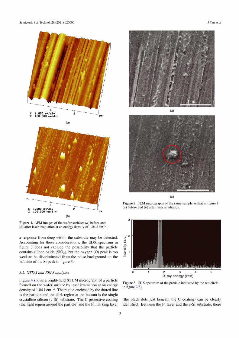
Figures 1(a) and (b) show AFM images of the wafer surfacebefore and after laser irradiation at an energy density of1.04 J cm−2, respectively. Before laser irradiation, numerousparallel microgrooves are visible on the surface (figure 1(a)).The microgrooves are a few tens of nanometers highand several hundreds of nanometers wide, giving anarithmetic average surface roughness of 10 nmRa, whilethe maximum height of the surface profile was 117 nmRy.These microgrooves were formed through scratching bydiamond abrasive grains during ductile-mode grinding. Themicrogrooves were significantly flattened after laser irradiation(figure 1(b)), although there were a few sharp protrusionson the surface. The protrusions range from a few tens ofnanometers to several hundreds of nanometers in size. Theseprotrusions caused the maximum height of the surface profileto increase to 121 nmRy, whereas the arithmetic averagesurface roughness decreased to 4 nmRa, which is considerablysmaller than that in figure 1(a).
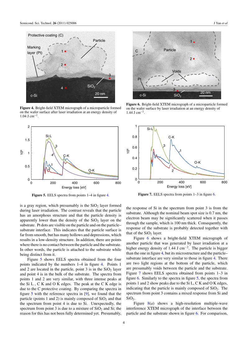
Figure 2 shows SEM micrographs of the same samples asthose in figure 1. Microgrooves are clearly observable on thesurface in figure 2(a). There are extremely small burrs andpile-ups of material on the sides of the grooves, indicating thatthe wafer surface was machined in a completely ductile mode(i.e. microscopic plastic flow of material dominated in thegrinding process). The microgrooves disappeared after laserirradiation (figure 2(b)) and irregular-shaped microparticles ofdifferent sizes appeared on the surface. The largest particle(indicated by the red circle in figure 2(b)) is approximately400 nm wide.
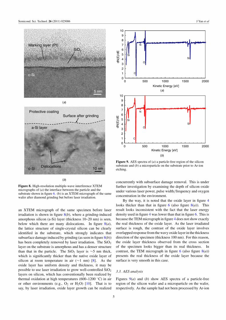
Figure 3 shows an EDX spectrum of the particle indicatedby the red circle in figure 2(b). A very intense peak due tosilicon (Si) is shown, whereas the peaks for other elementsare negligible. As no other elements were detected, it ispresumable that the particles are not contaminations fromthe environment or from the grinding process (i.e. fromthe diamond abrasive grains). It should be noted that thespectrum in figure 3 may contain a response from the substrate.Although the electron beam spot size was nominally 4 nm,the electron beam will be scattered considerably when itpasses through the particle. The spatial resolution of EDX isestimated to be 1 μm or larger. Moreover, as an electron beamcan penetrate to a depth of approximately 500 nm in silicon,
2
Semicond. Sci. Technol. 26 (2011) 025006 J Yan et al
(a)
(b)
Figure 1. AFM images of the wafer surface: (a) before and(b) after laser irradiation at an energy density of 1.04 J cm−2.
a response from deep within the substrate may be detected.Accounting for these considerations, the EDX spectrum infigure 3 does not exclude the possibility that the particlecontains silicon oxide (SiO2), but the oxygen (O) peak is tooweak to be discriminated from the noise background on theleft side of the Si peak in figure 3.
3.2. XTEM and EELS analyses
Figure 4 shows a bright-field XTEM micrograph of a particleformed on the wafer surface by laser irradiation at an energydensity of 1.04 J cm−2. The region enclosed by the dotted lineis the particle and the dark region at the bottom is the singlecrystalline silicon (c-Si) substrate. The C protective coating(the light region around the particle) and the Pt marking layer
1µm
(a)
1µm
(b)
Figure 2. SEM micrographs of the same sample as that in figure 1(a) before and (b) after laser irradiation.
X-ray energy (keV)
Inte
nsity
(a.
u.)
1
2
3
50 1 2 3 4
Figure 3. EDX spectrum of the particle indicated by the red circlein figure 2(b).
(the black dots just beneath the C coating) can be clearlyidentified. Between the Pt layer and the c-Si substrate, there
3
Semicond. Sci. Technol. 26 (2011) 025006 J Yan et al
20 nm
Protective coating (C)Particle
c-Si
SiO2
1
2
4
3
Marking
layer (Pt)
Figure 4. Bright-field XTEM micrograph of a microparticle formedon the wafer surface after laser irradiation at an energy density of1.04 J cm−2.
0
0.5
1
1.5
2
0 200 400 600 800Energy loss [eV]
×10
6
12
4
3
O-K
C-K
Si-L
Figure 5. EELS spectra from points 1–4 in figure 4.
is a gray region, which presumably is the SiO2 layer formedduring laser irradiation. The contrast reveals that the particlehas an amorphous structure and that the particle density isapparently lower than the density of the SiO2 layer on thesubstrate. Pt dots are visible on the particle and on the particle–substrate interface. This indicates that the particle surface isfar from smooth, but has many hollows and depressions, whichresults in a low-density structure. In addition, there are pointswhere there is no contact between the particle and the substrate.In other words, the particle is attached to the substrate whilebeing distinct from it.
Figure 5 shows EELS spectra obtained from the fourpoints indicated by the numbers 1–4 in figure 4. Points 1and 2 are located in the particle, point 3 is in the SiO2 layerand point 4 is in the bulk of the substrate. The spectra frompoints 1 and 2 are very similar, with three intense peaks atthe Si L , C K and O K edges. The peak at the C K edge isdue to the C protective coating. By comparing the spectra infigure 5 with the reference spectra in [9], we found that theparticle (points 1 and 2) is mainly composed of SiO2 and thatthe spectrum from point 4 is due to Si. Unexpectedly, thespectrum from point 3 is due to a mixture of SiO2 and Si; thereason for this has not been fully determined yet. Presumably,
20 nm
Particle
Pt
c-Si SiO2
1
2
3
Voids
C
Figure 6. Bright-field XTEM micrograph of a microparticle formedon the wafer surface by laser irradiation at an energy density of1.44 J cm−2.
0
0.2
0.4
0.6
0.8
1
0 200 400 600 800Energy loss [eV]
×10
6 1
2
3
O-K
C-K
Si-L
Figure 7. EELS spectra from points 1–3 in figure 6.
the response of Si in the spectrum from point 3 is from thesubstrate. Although the nominal beam spot size is 0.7 nm, theelectron beam may be significantly scattered when it passesthrough the sample, which is 100 nm thick. Consequently, theresponse of the substrate is probably detected together withthat of the SiO2 layer.
Figure 6 shows a bright-field XTEM micrograph ofanother particle that was generated by laser irradiation at ahigher energy density of 1.44 J cm−2. The particle is biggerthan the one in figure 4, but its microstructure and the particle–substrate interface are very similar to those in figure 4. Thereare two light regions at the bottom of the particle, whichare presumably voids between the particle and the substrate.Figure 7 shows EELS spectra obtained from points 1–3 infigure 6. Similarly to the spectra in figure 5, the spectra frompoints 1 and 2 show peaks due to the Si L, C K and O K edges,indicating that the particle is mainly composed of SiO2. Thespectrum from point 3 contains a mixed response from Si andSiO2.
Figure 8(a) shows a high-resolution multiple-waveinterference XTEM micrograph of the interface between theparticle and the substrate shown in figure 6. For comparison,
4
Semicond. Sci. Technol. 26 (2011) 025006 J Yan et al
5 nm
Marking layer (Pt)
c-Si
SiO2
(a)
10 nmDislocations
a-Si layer
Protective coatingSurface after grinding
c-Si
(b)
Figure 8. High-resolution multiple-wave interference XTEMmicrographs of (a) the interface between the particle and thesubstrate shown in figure 6. (b) is an XTEM micrograph of the samewafer after diamond grinding but before laser irradiation.
an XTEM micrograph of the same specimen before laserirradiation is shown in figure 8(b), where a grinding-inducedamorphous silicon (a-Si) layer (thickness 10–20 nm) is seen,below which there are many dislocations. In figure 8(a),the lattice structure of single-crystal silicon can be clearlyidentified in the substrate, which strongly indicates thatsubsurface damage induced by grinding (as seen in figure 8(b))has been completely removed by laser irradiation. The SiO2
layer on the substrate is amorphous and has a denser structurethan that in the particle. The SiO2 layer is ∼5 nm thick,which is significantly thicker than the native oxide layer ofsilicon at room temperature in air (∼1 nm) [8]. As theoxide layer has uniform density and thickness, it may bepossible to use laser irradiation to grow well-controlled SiO2
layers on silicon, which has conventionally been realized bythermal oxidation at high temperatures (600–1200 ◦C) in airor other environments (e.g., O2 or H2O) [10]. That is tosay, by laser irradiation, oxide layer growth can be realized
0
1
2
3
4
5
6
7
8
9
10
0 500 1000 1500 2000
dN(E
)/dE
Kinetic Energy [eV]
Si
O
N
C
Si
(a)
0
1
2
3
4
5
6
7
8
9
10
0 500 1000 1500 2000
dN(E
)/dE
Kinetic Energy [eV]
Si
O
N
C
Si
(b)
Figure 9. AES spectra of (a) a particle-free region of the siliconsubstrate and (b) a microparticle on the substrate prior to Ar-ionetching.
concurrently with subsurface damage removal. This is underfurther investigation by examining the depth of silicon oxideunder various laser power, pulse width/frequency and oxygenconcentration in the environment.
By the way, it is noted that the oxide layer in figure 4looks thicker than that in figure 6 (also figure 8(a)). Thisresult looks inconsistent with the fact that the laser energydensity used in figure 4 was lower than that in figure 6. This isbecause the TEM micrograph in figure 4 does not show exactlythe real thickness of the oxide layer. As the laser irradiatedsurface is rough, the contrast of the oxide layer involvesoverlapped response from the wavy oxide layer in the thicknessdirection of the specimen (thickness 100 nm). For this reason,the oxide layer thickness observed from the cross sectionof the specimen looks bigger than its real thickness. Incontrast, the TEM micrograph in figure 6 (also figure 8(a))presents the real thickness of the oxide layer because thesurface is very smooth in this case.
3.3. AES analysis
Figures 9(a) and (b) show AES spectra of a particle-freeregion of the silicon wafer and a microparticle on the wafer,respectively. As the sample had not been processed by Ar-ion
5
Semicond. Sci. Technol. 26 (2011) 025006 J Yan et al
0
1
2
3
4
5
6
7
8
9
10
0 500 1000 1500 2000
dN(E
)/dE
Kinetic Energy [eV]
Si
O
Si
Ar SiC
(a)
0
1
2
3
4
5
6
7
8
9
10
0 500 1000 1500 2000
dN(E
)/dE
Kinetic Energy [eV]
SiO
Si
C
Ar
Si
(b)
Figure 10. AES spectra of the same sample as that in figure 9 after ithad been processed by Ar-ion etching: (a) substrate and (b) particle.
etching, the spectra in figure 9 are the responses mainly fromthe surfaces of the substrate and the particle. The two spectraare very similar, both showing strong responses at typicalkinetic energies of Si, O and C [11]. These results indicatethat both the particle and the wafer surface consist of SiO2,though the composition ratio between Si and O obtained fromthe AES spectra shown in figure 9 is 1:1.2, higher than thestoicheiometric composition of SiO2 (1:2). The particle has aloose structure, thus the Auger electrons are generated not onlyfrom particle surface (mainly SiO2), but also from the dottedsilicon grains in the particle, and from the silicon substratebelow the particle. The peaks of C are due to the protectivecoating, and the peaks of nitrogen (N) in these spectra maybe due to organic contamination from the environment priorto depositing C and Pt. Another possible reason of the Npeaks might be nitridation of silicon during laser irradiation.As the laser irradiation tests were performed in air, the hightemperature might have caused slight nitridation of silicon.
Figure 10 shows AES spectra of the same sample as that infigure 9 except that the sample had been processed by Ar-ionetching prior to AES analysis. In this case, the AES spectrawere obtained mainly from within the substrate and particle.The response from the residual particle surface might alsobe detected because the Ar-ion etching could not removecompletely the entire surface layer of a particle with irregular
Low-densitySiO2
a-Si
SiO2
c-Si
Low-densitySiO2
Figure 11. Schematic model of the laser-induced microparticles andoxide layer.
shape. In both figures 10(a) and (b), the Si peak is more intensethan in figure 9, whereas the O peak intensity is considerablysmaller. In particular, the O peak in figure 10(a) is almostnonexistent. This result demonstrates that the particle containsSi in the interior region and SiO2 in the outside region.
3.4. Particle formation mechanism
The calculation in [7] revealed that the wafer surfacetemperature increases with increasing laser energy density.When the laser energy density is 0.96 J cm−2, the wafer surfacetemperature is 3028 ◦C, which is higher than the boiling pointof silicon (2878 ◦C) [12]. The results obtained in this studyprovide new evidence for silicon boiling. That is, silicon at thesurface boils and forms small droplets. After the laser pulsefinishes, these droplets resolidify and reattach to the surface.At the same time, both the substrate and particles are oxidized.As the droplets are recondensed and oxidized in free space,the resulting particles have a less dense structure than the SiO2
film that forms on the substrate. In addition, oxidization maybe incomplete in a few droplets, especially the bigger ones. Inthis case, silicon grains with amorphous structures may remainin the resulting particles. Figure 11 schematically depicts astructural model of the particles and oxide layer.
3.5. Particle removal
Particle generation can be prevented using a lower laser energydensity (<0.96 J cm−2) [7]. When this is done, silicon meltswithout boiling so that the subsurface damage is removedwithout forming unwanted particles. However, particles willbe generated when high laser energy densities are required(e.g., to process wafers with deep damage and rough surfaces)and they must be removed by employing subsequent processes.
In this study, hydrofluoric (HF) acid etching wasperformed on samples with laser-generated particles. Theetchant used was 1 wt% HF. The etching time was set to 20 min,which was estimated based on the etching rate (∼0.1 nm s−1)of thermally formed SiO2 [8]. After etching, the sampleswere washed in flowing pure water for 5 min before SEMobservations. Figures 12(a) and (b) show SEM micrographs
6
Semicond. Sci. Technol. 26 (2011) 025006 J Yan et al
1µm
(a)
1µm
(b)
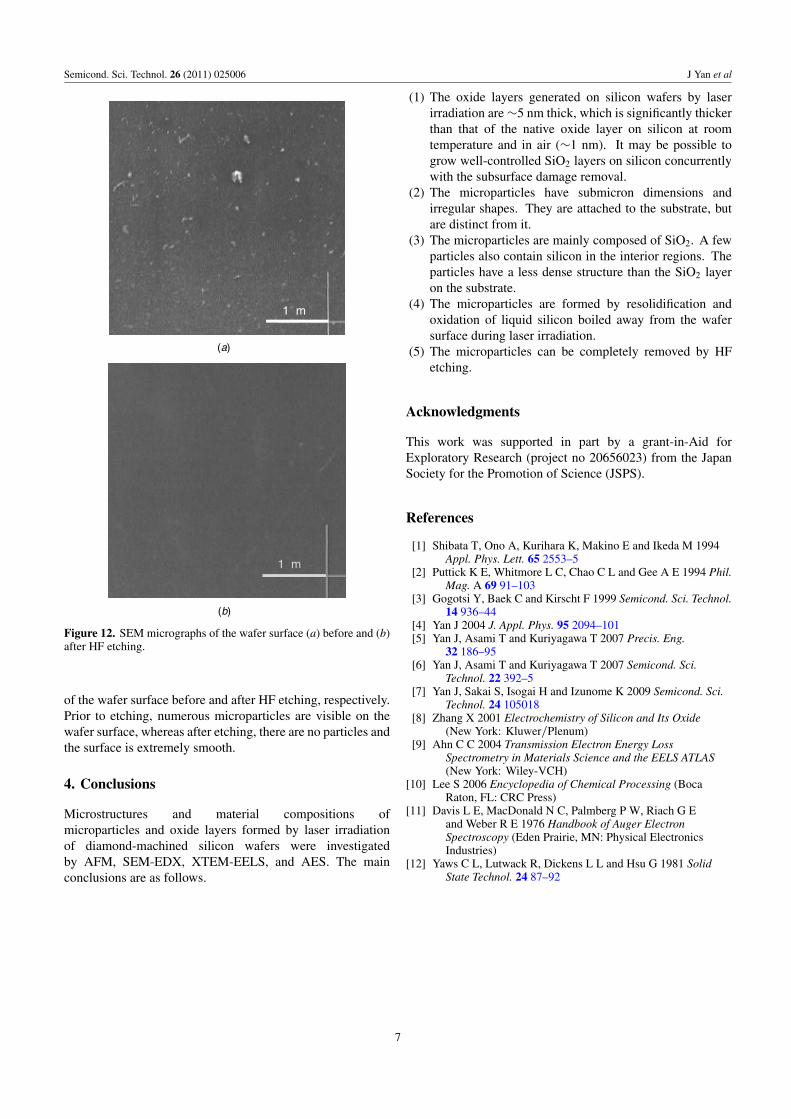
Figure 12. SEM micrographs of the wafer surface (a) before and (b)after HF etching.
of the wafer surface before and after HF etching, respectively.Prior to etching, numerous microparticles are visible on thewafer surface, whereas after etching, there are no particles andthe surface is extremely smooth.
4. Conclusions
Microstructures and material compositions ofmicroparticles and oxide layers formed by laser irradiationof diamond-machined silicon wafers were investigatedby AFM, SEM-EDX, XTEM-EELS, and AES. The mainconclusions are as follows.
(1) The oxide layers generated on silicon wafers by laserirradiation are ∼5 nm thick, which is significantly thickerthan that of the native oxide layer on silicon at roomtemperature and in air (∼1 nm). It may be possible togrow well-controlled SiO2 layers on silicon concurrentlywith the subsurface damage removal.
(2) The microparticles have submicron dimensions andirregular shapes. They are attached to the substrate, butare distinct from it.
(3) The microparticles are mainly composed of SiO2. A fewparticles also contain silicon in the interior regions. Theparticles have a less dense structure than the SiO2 layeron the substrate.
(4) The microparticles are formed by resolidification andoxidation of liquid silicon boiled away from the wafersurface during laser irradiation.
(5) The microparticles can be completely removed by HFetching.
Acknowledgments
This work was supported in part by a grant-in-Aid forExploratory Research (project no 20656023) from the JapanSociety for the Promotion of Science (JSPS).
References
[1] Shibata T, Ono A, Kurihara K, Makino E and Ikeda M 1994Appl. Phys. Lett. 65 2553–5
[2] Puttick K E, Whitmore L C, Chao C L and Gee A E 1994 Phil.Mag. A 69 91–103
[3] Gogotsi Y, Baek C and Kirscht F 1999 Semicond. Sci. Technol.14 936–44
[4] Yan J 2004 J. Appl. Phys. 95 2094–101[5] Yan J, Asami T and Kuriyagawa T 2007 Precis. Eng.
32 186–95[6] Yan J, Asami T and Kuriyagawa T 2007 Semicond. Sci.
Technol. 22 392–5[7] Yan J, Sakai S, Isogai H and Izunome K 2009 Semicond. Sci.
Technol. 24 105018[8] Zhang X 2001 Electrochemistry of Silicon and Its Oxide
(New York: Kluwer/Plenum)[9] Ahn C C 2004 Transmission Electron Energy Loss
Spectrometry in Materials Science and the EELS ATLAS(New York: Wiley-VCH)
[10] Lee S 2006 Encyclopedia of Chemical Processing (BocaRaton, FL: CRC Press)
[11] Davis L E, MacDonald N C, Palmberg P W, Riach G Eand Weber R E 1976 Handbook of Auger ElectronSpectroscopy (Eden Prairie, MN: Physical ElectronicsIndustries)
[12] Yaws C L, Lutwack R, Dickens L L and Hsu G 1981 SolidState Technol. 24 87–92
7


![Research Article Preparation and Characterization of ...of cubic -Fe 2 O 3 (hematite) microparticles via a simple one-step hydrothermal reaction [ ]. Iron and iron oxide nanoparticles](https://img.dokumen.tips/doc/110x75/60f74baac7869246ca625f4e/research-article-preparation-and-characterization-of-of-cubic-fe-2-o-3-hematite.jpg)