Embed Size (px)
Citation preview

Introduction Power Semiconductor ApplicationsPhilips Semiconductors
CHAPTER 1
Introduction to Power Semiconductors
1.1 General
1.2 Power MOSFETS
1.3 High Voltage Bipolar Transistors
1


Introduction Power Semiconductor ApplicationsPhilips Semiconductors
General
3

Introduction Power Semiconductor ApplicationsPhilips Semiconductors
1.1.1 An Introduction To Power Devices
Today’s mains-fed switching applications make use of awide variety of active power semiconductor switches. Thischapter considers the range of power devices on the markettoday, making comparisons both in terms of their operationand their general areas of application. The P-N diode willbe considered first since this is the basis of all activeswitches. This will be followed by a look at both 3 layer and4 layer switches.
Before looking at the switches let’s briefly consider thevarious applications in which they are used. Virtually allmains fed power applications switch a current through aninductive load. This is the case even for resonant systemswhere the operating point is usually on the "inductive" sideof the resonance curve. The voltage that the switch isnormally required to block is, in the majority of cases, oneor two times the maximum rectified input voltage dependingon the configuration used. Resonant applications are theexception to this rule with higher voltages being generatedby the circuit. For 110-240 V mains, the required voltageratings for the switch can vary from 200 V to 1600 V.
Under normal operating conditions the off-state losses inthe switch are practically zero. For square wave systems,the on-state losses (occurring during the on-time), areprimarily determined by the on-state resistance which givesrise to an on-state voltage drop, VON. The (static) on-statelosses may be calculated from:
At the end of the "ON" time the switch is turned off. Theturn-off current is normally high which gives rise to a lossdependent on the turn-off properties of the switch. Theprocess of turn-on will also involve a degree of power lossso it is important not to neglect the turn-on properties either.Most applications either involve a high turn-on current orthe current reaching its final value very quickly (high dI/dt).The total dynamic power loss is proportional to both thefrequency and to the turn-on and turn-off energies.
The total losses are the sum of the on-state and dynamiclosses.
The balance of these losses is primarily determined by theswitch used. If the on-state loss dominates, operatingfrequency will have little influence and the maximumfrequency of the device is limited only by its total delay time(the sum of all its switching times). At the other extreme adevice whose on-state loss is negligible compared with theswitching loss, will be limited in frequency due to theincreasing dynamic losses.
Fig.1 Cross section of a silicon P-N diode
High frequency switching When considering frequencylimitation it is important to realise that the real issue is notjust the frequency, but also the minimum on-time required.For example, an SMPS working at 100 kHz with an almostconstant output power, will have a pulse on-time tP of about2-5 µs. This can be compared with a high performance UPSworking at 10 kHz with low distortion which also requires aminimum on-time of 2 µs. Since the 10 kHz and 100 kHzapplications considered here, require similar shorton-times, both may be considered high frequencyapplications.
Resonant systems have the advantage of relaxing turn-onor turn-off or both. This however tends to be at the expenseof V-A product of the switch. The relaxed switchingconditions imply that in resonant systems switches can beused at higher frequencies than in non resonant systems.When evaluating switches this should be taken intoaccount.
P
N
CATHODE
ANODE
PSTATIC= δ.VON.ION (1)
PDYNAMIC = f .(EON + EOFF) (2)
PTOT = δ.VON.ION + f .(EON + EOFF) (3)
5

Introduction Power Semiconductor ApplicationsPhilips Semiconductors
Fig.2 Field distribution in the N- layer
E
HIGH RESISTIVITY
Thickness
E
Thickness
LOW RESITIVITY
E
INTERMEDIATE CASE
Thickness
Case 1 Case 2 Case 3
At higher values of throughput power, the physical size ofcircuits increases and as a consequence, the strayinductances will also tend to increase. Since the requiredcurrents are higher, the energy stored in the strayinductances rises significantly, which in turn means theinduced peak voltages also rise. As a result suchapplications force the use of longer pulse times, to keeplosses down, and protection networks to limit overshoot ornetworks to slow down switching speeds. In addition theuse of larger switches will also have consequences in termsof increasing the energy required to turn them on and offand drive energy is very important.
So, apart from the voltage and current capabilities ofdevices, it is necessary to consider static and dynamiclosses, drive energy, dV/dt, dI/dt and Safe Operating Areas.
The silicon diodeSilicon is the semiconductor material used for all powerswitching devices. Lightly doped N- silicon is usually takenas the starting material. The resistance of this materialdepends upon its resistivity, thickness and total area.
A resistor as such does not constitute an active switch, thisrequires an extra step which is the addition of a P-layer.The result is a diode of which a cross section is drawn inFig.1
The blocking diodeSince all active devices contain a diode it is worthconsidering its structure in a little more detail. To achievethe high blocking voltages required for active powerswitches necessitates the presence of a thick N- layer. Towithstand a given voltage the N- layer must have the right
combination of thickness and resistivity. Some flexibilityexists as to what that combination is allowed to be, theeffects of varying the combination are described below.
Case 1: Wide N- layer and low resistivity
Figure 2 gives the field profile in the N- layer, assuming thejunction formed with the P layer is at the left. The maximumfield at the P-N junction is limited to 22 kV/cm by thebreakdown properties of the silicon. The field at the otherend is zero. The slope of the line is determined by theresistivity. The total voltage across the N- layer is equal tothe area underneath the curve. Please note that increasingthe thickness of the device would not contribute to itsvoltage capability in this instance. This is the normal fieldprofile when there is another P-layer at the back as in 4layer devices (described later).
Case 2: Intermediate balance
In this case the higher resistivity material reduces the slopeof the profile. The field at the junction is the same so thesame blocking voltage capability (area under the profile)can be achieved with a thinner device.The very steep profile at the right hand side of the profileindicates the presence of an N+ layer which often requiredto ensure a good electrical contact
Case 3: High resistivity material
With sufficiently high resistivity material a near horizontalslope to the electric field is obtained. It is this scenario whichwill give rise to the thinnest possible devices for the samerequired breakdown voltage. Again an N+ layer is requiredat the back.
An optimum thickness and resistivity exists which will givethe lowest possible resistance for a given voltagecapability.Both case 1 (very thick device) and case 3 (high resistivity)give high resistances, the table below shows the thicknessand resistivity combinations possible for a 1000 V diode.
R = ρ.lA
(4)
6

Introduction Power Semiconductor ApplicationsPhilips Semiconductors
The column named RA gives the resistance area product.(A device thickness of less than 50 µm will never yield1000 V and the same goes for a resistivity of less than26 Ωcm.) The first specification is for the thinnest devicepossible and the last one is for the thickest device, (requiredwhen a P layer is present at the back). It can be seen thatthe lowest resistance is obtained with an intermediate valueof resistivity and material thickness.
Thickness Resistivity RA Comments
(µm) (Ωcm) Ωcm2
50 80 0.400 case 3
60 34 0.204
65 30 0.195
70 27 0.189 min. R
75 26 0.195
80 26 0.208
90 26 0.234
100 26 0.260 case 1
To summarise, a designer of high voltage devices has onlya limited choice of material resistivity and thickness withwhich to work. The lowest series resistance is obtained fora material thickness and resistivity intermediate betweenthe possible extremes. This solution is the optimum for allmajority carrier devices such as the PowerMOSFET andthe J-FET where the on-resistance is uniquely defined bythe series resistance. Other devices make use of chargestorage effects to lower their on-state voltage.Consequently to optimise switching performance in thesedevices the best choice will be the thinnest layer such thatthe volume of stored charge is kept to a minimum. Finallyas mentioned earlier, the design of a 4 layer device requiresthe thickest, low resistivity solution.
The forward biased diodeWhen a diode is forward biased, a forward current will flow.Internally this current will have two components: an electroncurrent which flows from the N layer to the P layer and ahole current in the other direction. Both currents willgenerate a charge in the opposite layer (indicated with QP
and QN in Fig.3). The highest doped region will deliver mostof the current and generate most of the charge. Thus in aP+ N- diode the current will primarily be made up of holesflowing from P to N and there will be a significant volumeof hole charge in the N- layer. This point is important whendiscussing active devices: whenever a diode is forwardbiased (such as a base-emitter diode) there will be a chargestored in the lowest doped region.
Fig. 3 Diode in forward conduction
The exact volume of charge that will result is dependentamongst other things on the minority carrier lifetime, τ.Using platinum or gold doping or by irradiation techniquesthe value of τ can be decreased. This has the effect ofreducing the volume of stored charge and causing it todisappear more quickly at turn-off. A side effect is that theresistivity will increase slightly.
Three Layer devices
The three basic designs, which form the basis for all derived3 layer devices, are given in Fig.4. It should be emphasisedhere that the discussion is restricted to high voltage devicesonly as indicated in the first section. This means that allrelevantdevices will have a vertical structure, characterisedby a wide N--layer.
The figure shows how a three layer device can be formedby adding an N type layer to the P-N diode structure. Twoback to back P-N diodes thus form the basis of the device,where the P layer provides a means to control the currentwhen the device is in the on-state.
There are three ways to use this P-layer as a controlterminal. The first is to feed current into the terminal itself.The current through the main terminals is now proportionalto the drive current. This device is called a High VoltageTransistor or HVT.
The second one is to have openings in the P-layer andpermit the main current to flow between them. Whenreverse biasing the gate-source, a field is generated whichblocks the opening and pinches off the main current. Thisdevice is known as the J-FET (junction FET) or SIT (StaticInduction Transistor).
P
CATHODE
ANODE
Ip IN
QP
QN
N
N
-
+
7

Introduction Power Semiconductor ApplicationsPhilips Semiconductors
Fig.4 The three basic three layer devices
P
N
EMITTER
COLLECTOR
-
N
BASE
P
N
SOURCE
DRAIN
-
N
GATE
P
N
SOURCE
DRAIN
-
N
GATE
BIPOLAR TRANSISTOR J-FET (SIT) MOS
N N N
The third version has an electrode (gate) placed very closeto the P-layer. The voltage on this gate pushes away theholes in the P-area and attracts electrons to the surfacebeneath the gate. A channel is thus formed between themain terminals so current can flow. The well known namefor this device is MOS transistor.
In practice however, devices bear little resemblance to theconstructions of Fig.4. In virtually all cases a planarconstruction is chosen i.e. the construction is such that onemain terminal (emitter or source) and the drive contact areon the surface of the device. Each of the devices will nowbe considered in some more detail.
The High Voltage Transistor (HVT)The High Voltage Transistor uses a positive base currentto control the main collector current. The relation is:IC = HFE * IB. Thebase drive forward biases the base emitterP-N junction and charge (holes and electrons) will passthrough it. Now the base of a transistor is so thin that themost of the electrons do not flow to the base but into thecollector - giving rise to a collector current. As explainedpreviously, the ratio between the holes and electronsdepend on the doping. So by correctly doping the baseemitter junction, the electron current can be made muchlarger than the hole current, which means that IC can bemuch larger than IB.
When enough base drive is provided it is possible to forwardbias the base-collector P-N junction also. This has asignificant impact on the resistance of the N- layer; holesnow injected from the P type base constitute stored chargecausing a substantial reduction in on-state resistance,much lower than predicted by equation 4. Under theseconditions the collector is an effective extension of the base.Unfortunately the base current required to maintain this
Fig.5 The HVT
condition causes the current gain to drop. For this reasonone cannot use a HVT at a very high current densitybecause then the gain would become impractically low.
The on-state voltage of an HVT will be considerably lowerthan for a MOS or J-FET. This is its main advantage, butthe resulting charge stored in the N- layer has to bedelivered and also to be removed. This takes time and thespeed of a bipolar transistor is therefore not optimal. Toimprove speed requires optimisation of a fine emitterstructure in the form of fingers or cells.
Both at turn-on and turn-off considerable losses may occurunless care is taken to optimise drive conditions. At turn-ona short peak base current is normally required. At turn-offa negative base current is required and negative drive hasto be provided.
P
COLLECTOR
B B BE E
N
N
-
+
N+ N+
IB
Electrons
8
Introduction Power Semiconductor ApplicationsPhilips Semiconductors
A serious limitation of the HVT is the occurrence of secondbreakdown during switch off. The current contracts towardsthe middle of the emitter fingers and the current density canbecome very high. The RBSOAR (Reverse Bias SafeOperating Area) graph specifies where the device can beused safely. Device damage may result if the device is notproperly used and one normally needs a snubber (dV/dtnetwork) to protect the device. The price of such a snubberis normally in the order of the price of the transistor itself.In resonant applications it is possible to use the resonantproperties of the circuit to have a slow dV/dt.
So, the bipolar transistor has the advantage of a very lowforward voltage drop, at the cost of lower speed, aconsiderable energy is required to drive it and there arealso limitations in the RBSOAR.
The J-FET.
The J-FET (Junction Field Effect Transistor) has a directresistance between the Source and the Drain via theopening in the P-layer. When the gate-source voltage iszero the device is on. Its on-resistance is determined by theresistance of the silicon and no charge is present to makethe resistance lower as in the case of the bipolar transistor.When a negative voltage is applied between Gate andSource, a depletion layer is formed which pinches off thecurrent path. So, the current through the switch isdetermined by the voltage on the gate. The drive energy islow, it consists mainly of the charging and discharging ofthe gate-source diode capacitance. This sort of device isnormally very fast.
Fig.6 The J-FET
Its main difficulty is the opening in the P-layer. In order tospeed up performance and increase current density, it isnecessary to make a number of openings and this impliesfine geometries which are difficult to manufacture. Asolution exists in having the P-layer effectively on thesurface, basically a diffused grid as shown in Fig.6.Unfortunately the voltages now required to turn the deviceoff may be very large: it is not uncommon that a voltage of25 V negative is needed. This is a major disadvantagewhich, when combined with its "normally-on" property andthe difficulty to manufacture, means that this type of deviceis not in mass production.
The MOS transistor.The MOS (Metal Oxide Semiconductor) transistor isnormally off: a positive voltage is required to induce achannel in the P-layer. When a positive voltage is appliedto the gate, electrons are attracted to the surface beneaththe gate area. In this way an "inverted" N-type layer isforced in the P-material providing a current path betweendrain and source.
Fig.7 The MOS transistor
Modern technology allows a planar structure with verynarrow cells as shown in Fig.7. The properties are quitelike the J-FET with the exception that the charge is nowacross the (normally very thin) gate oxide. Charging anddischarging the gate oxide capacitance requires drivecurrents when turning on and off. Switching speeds canbe controlled by controlling the amount of drive chargeduring the switching interval. Unlike the J-FET it does notrequire a negative voltage although a negative voltage mayhelp switch the device off quicker.
The MOSFET is the preferred device for higher frequencyswitching since it combines fast speed, easy drive and widecommercial availability.
DRAIN
S G
N
N
-
+
S
N+ N+P P
DRAIN
G G GS S
P PPN+ N+
N
N
-
+
9
Introduction Power Semiconductor ApplicationsPhilips Semiconductors
Refinements to the basic structureA number of techniques are possible to improve uponbehaviour of the basic device.
First, the use of finer geometries can give lower on-statevoltages, speed up devices and extend their energyhandling capabilities. This has led to improved"Generation 3" devices for bipolars and to lower RDS(ON) forPowerMOS. Secondly, killing the lifetime τ in the devicecan also yield improvements. For bipolar devices, thispositively effects the switching times. The gain, however,will drop, and this sets a maximum to the amount of lifetimekilling. For MOS a lower value for τ yields the so-calledFREDFETs, with an intrinsic diode fast enough for manyhalf bridge applications such as in AC Motor Controllers.The penalty here is that RDS(ON) is adversely effected(slightly). Total losses, however, are decreasedconsiderably.
Four layer devicesThe three basic designs from the previous section can beextended with a P+-layer at the back, thereby generatingthree basic Four Layer Devices. The addition of this extralayer creates a PNP transistor from the P+-N--P-layers. Inall cases the 3 layer NPN device will now deliver an electroncurrent into the back P+-layer which acts as an emitter. ThePNP transistor will thus become active which results in ahole current flowing from the P+-layer into the high resistiveregion. This in its turn will lead to a hole charge in the highresistive region which lowers the on-state voltageconsiderably, as outlined above for High VoltageTransistors. Again, the penalty is in the switching timeswhich will increase.
All the devices with an added P+-layer at the back will injectholes into the N--layer. Since the P+-layer is much heavierdoped than the N--layer, this hole current will be the majorcontributor to the main current. This means that the chargein the N--layer, especially near the N--P+-junction, will belarge. Under normal operation the hole current will be largeenough to influence the injection of electrons from the topN+-layer. This results in extra electron current beinginjected from the top, leading to extra hole current from theback etc. This situation is represented in the schematic ofFig.8.
An important point is latching. This happens when theinternal currents are such that we are not able to turn offthe device using the control electrode. The only way to turnit off is by externally removing the current from the device.
The switching behaviour of all these devices is affected bythe behaviour of the PNP: as long as a current is flowingthrough the device, the back will inject holes into theN--layer. This leads to switching tails which contributeheavily to switching losses. The tail is strongly affected bythe lifetime τ and by the application of negative drive current
when possible. As previously explained, adjustment of thelifetime affects the on-state voltage. Carefully adjusting thelifetime τ will balance the on-state losses with the switchinglosses.
All four layer devices show this trade-off between switchinglosses and on-state losses. When minimising switchinglosses, the devices are optimised for high frequencyapplications. When the on-state losses are lowest thecurrent density is normally highest, but the device is onlyuseful at low frequencies. So two variants of the four layerdevice generally exist. In some cases intermediate speedsare also useful as in the case of very high power GTOs.
The Thyristor
A thyristor (or SCR, Silicon Controlled Rectifier) isessentially an HVT with an added P+-layer. The resultingP--N--P+ transistor is on when the whole device is on andprovides enough base current to the N+-P-N- transistor tostay on. So after an initial kick-on, no further drive energyis required.
Fig.8 Thyristor
The classical thyristor is thus a latching device. Itsconstruction is normally not very fine and as a result thegate contact is too far away from the centre of the activearea to be able to switch it off. Also the current density ismuchhigher than ina bipolar transistor. The switching timeshowever are very long. Its turn-on is hampered by itsstructure since it takes quite a while for the whole crystalto become active. This seriously limits its dI/dt.
Once a thyristor is on it will only turn-off after having zerocurrent for a few microseconds. This is done by temporarilyforcing the current via a so-called commutation circuit.
P
ANODE
G GC
P+
N-
N+
Ip2
Ip1
10

Introduction Power Semiconductor ApplicationsPhilips Semiconductors
The charge in the device originates from two sources: Thestandard NPN transistor structure injects holes in theN--layer (IP1 in Fig.8) and the PNP transistor injects a chargefrom the back (IP2 in Fig.8). Therefore the total charge is bigand switching performance is very poor. Due to its slowswitching a normal thyristor is only suitable up to a few kHz.
A major variation on the thyristor is the GTO (Gate Turn OffThyristor). This is a thyristor where the structure has beentailored to give better speed by techniques suchas accuratelifetime killing, fine finger or cell structures and "anodeshorts" (short circuiting P+ and N- at the back in order todecrease the current gain of the PNP transistor).As a result,the product of the gain of both NPN and PNP is just sufficientto keep the GTO conductive. A negative gate current isenough to sink the hole current from the PNP and turn thedevice off.
Fig.9 The GTO
A GTO shows much improved switching behaviour but stillhas the tail as described above. Lower power applications,especially resonant systems, are particularly attractive forthe GTO because the turn-off losses are virtually zero.
The SIThThe SITh (Static Induction Thyristor) sometimes alsoreferred to as FCT (Field Controlled Thyristor) is essentiallya J-FET with an added P+ back layer. In contrast to thestandard thyristor, charge is normally only injected from theback, so the total amount of charge is limited. However, apositive gate drive is possible which will reduce on-stateresistance.
Active extraction of charge via the gate contact is possibleand switching speeds may be reduced considerably byapplying an appropriate negative drive as in the case of anHVT. As for the SIT the technological complexity is a severe
Fig.10 The SITh
drawback, as is its negative drive requirements.Consequently mass production of this device is notavailable yet.
The IGBT
An IGBT (Insulated Gate Bipolar Transistor) is an MOStransistor with P+ at the back. Charge is injected from theback only, which limits the total amount of charge. Activecharge extraction is not possible, so the carrier lifetime τshould be chosen carefully, since that determines theswitching losses. Again two ranges are available with bothfast and slow IGBTs.
Fig.11 The IGBT
ANODE
G G GC C
P PPN+ N+
N
P
-
+
P
ANODE
G G GC C
N
P
-
+
N+ N+
N+ N+
COLLECTOR
E G
N-
E
N+ N+P P
P+
11

Introduction Power Semiconductor ApplicationsPhilips Semiconductors
The speed of the fast IGBT is somewhat better than that ofa GTO because a similar technology is used to optimisethe IGBT but only the back P+-layer is responsible for thecharge.
The IGBT is gaining rapidly in popularity since itsmanufacturing is similar to producing PowerMOS and anincreasing market availability exists. Although the latchingof IGBTswas seen as aproblem,modern optimised devicesdon’t suffer from latch-up in practical conditions.
Refinements to the basic structure
The refinements outlined for 3 layer devices also apply to4 layer structures. In addition to these, an N+-layer may beinserted between the P+ and N--layer. Without such a layerthe designer is limited in choice of starting material to Case3 as explained in the diode section. Adding the extraN+-layer allows another combination of resistivity andthickness to be used, improving device performance. Anexample of this is the ASCR, the Asymmetric SCR, whichis much faster than normal thyristors. The reverse blockingcapability, however, is now reduced to a value of 10-20 V.
Comparison of the Basic Devices.It is important to consider the properties of devicesmentioned when choosing the optimum switch for aparticular application. Table 2 gives a survey of theessential device properties of devices capable ofwithstanding 1000 V. IGBTs have been classed in termsof fast and slow devices, however only the fast GTO andslow thyristor are represented. The fast devices areoptimised for speed, the slow devices are optimised for Onvoltage.
Comments
This table is valid for1000 V devices. Lowervoltagedeviceswill always perform better, higher voltage devices areworse.
A dot means an average value in between "+" and "-"
The "(--)" for a thyristor means a "--" in cases where forcedcommutation is used; in case of natural commutation it is"+"
Most figures are for reference only: in exceptional casesbetter performance has been achieved, but the figuresquoted represent the state of the art.
HVT J-FET MOS THY GTO IGBT IGBT Unitslow fast
V(ON) 1 10 5 1.5 3 2 4 V
Positive Drive Requirement - + + + + + + + = Simple toimplement
Turn-Off requirement - - + (--) - + + + = Simple toimplement
Drive circuit complexity - . + (-) . + + - = complex
Technology Complexity + . . + - - - - = complex
Device Protection - . + + - - - + = Simple toimplement
Delay time (ts, tq) 2 0.1 0.1 5 1 2 0.5 µs
Switching Losses . ++ ++ -- - - . + = good
Current Density 50 12 20 200 100 50 50 A/cm2
Max dv/dt (Vin = 0) 3 20 10 0.5 1.5 3 10 V/ns
dI/dt 1 10 10 1 0.3 10 10 A/ns
Vmax 1500 1000 1000 5000 4000 1000 1000 V
Imax 1000 10 100 5000 3000 400 400 A
Over Current factor 5 3 5 15 10 3 3
12
Introduction Power Semiconductor ApplicationsPhilips Semiconductors
Merged devicesMerged devices are the class of devices composed of twoor more of the above mentioned basic types. They don’toffer any breakthrough in device performance. This isunderstandable since the basic properties of the discusseddevices are not or are hardly effected. They may bebeneficial for the user though, primarily because they mayresult in lower positive and/or negative drive requirements.
Darlingtons and BiMOSA darlington consists of two bipolar transistors. The emittercurrent of the first (the driver) forms the base current of theoutput transistor. The advantages of darlingtons may besummarised as follows. A darlington has a higher gain thana single transistor. It also switches faster because the inputtransistor desaturates the output transistor and lowerswitching losses are the result. However, the resultingVCE(sat) is higher. The main issue, especially for higherpowers is the savings in drive energy. This means thatdarlingtons can be used at considerably higher outputpowers than standard transistors. Modern darlingtons inhigh power packages can be used in 20 kHz motor drivesand power supplies.
A BiMOS consists of a MOS driver and a bipolar outputtransistor. The positive drive is the same as MOS butturn-off is generally not so good. Adding a "speed-up" diodecoupled with some negative drive improves things.
Fig.12 The MCT
MCTMCT stands for MOS Controlled Thyristor. This device iseffectively a GTO with narrow tolerances, plus a P-MOStransistor between gate and source (P+-N-P MOS, the lefthand gate in Fig.12) and an extra N-MOS to turn it on, theN-P-N--MOS shown underneath the right hand gate.
Where the GTO would like to be switched off with a negativegate, the internal GTO in an MCT can turn off by shortcircuiting its gate-cathode, due to its fine structure. Its drivetherefore is like a MOS transistor and its behaviour similarto a GTO. Looking closely at the device it is obvious thata GTO using similar fine geometries with a suitable externaldrive can always perform better, at the cost of some drivecircuitry. The only plus point seems to be its ease of drive.
Application areas of the various devices
The following section gives an indication of where thevarious devices are best placed in terms of applications. Itis possible for circuit designers to use various tricks tointegrate devices and systems in innovative manners,applying devices far outside their ’normal’ operatingconditions. As an example, it is generally agreed that above100 kHz bipolars are too difficult to use. However, a450 kHz converter using bipolars has been alreadydescribed in the literature.
As far as the maximum frequency is concerned a numberof arguments must be taken into account.
First the delay times, either occurring at turn-on or atturn-off, will limit the maximum operating frequency. Areasonable rule of thumb for this is fMAX = 3 / tDELAY. (Thereis a danger here for confusion: switching times tend todepend heavily on circuit conditions, drive of the device andon current density. This may lead to a very optimistic orpessimistic expectation and care should be taken toconsider reasonable conditions.)
Another factor is the switching losseswhich areproportionalto the frequency. These power losses may be influencedby optimising the drive or by the addition of external circuitssuch as dV/dt or dI/dt networks. Alternatively the heatsinksize may be increased or one may choose to operatedevices at a lower current density in order to decreasepower losses. It isclear that thisargument isvery subjective.
A third point is manufacturability. The use of fine structuresfor example, which improves switching performance, ispossible only for small silicon chip sizes: larger chips withvery fine MOS-like structures will suffer from unacceptablelow factory yields. Therefore high power systems requiringlarge chip areas are bound to be made with less finestructures and will consequently be slower.
The operating current density of the device will influenceits physical size. A low current density device aimed at highpower systems would need a large outline which tends tobeexpensive. Large outlines also increase the physical sizeof the circuit, which leads to bigger parasitic inductancesand associated problems.
ANODE
N
P
-
+
N
G C G
P+P+N N+
P
13
Introduction Power Semiconductor ApplicationsPhilips Semiconductors
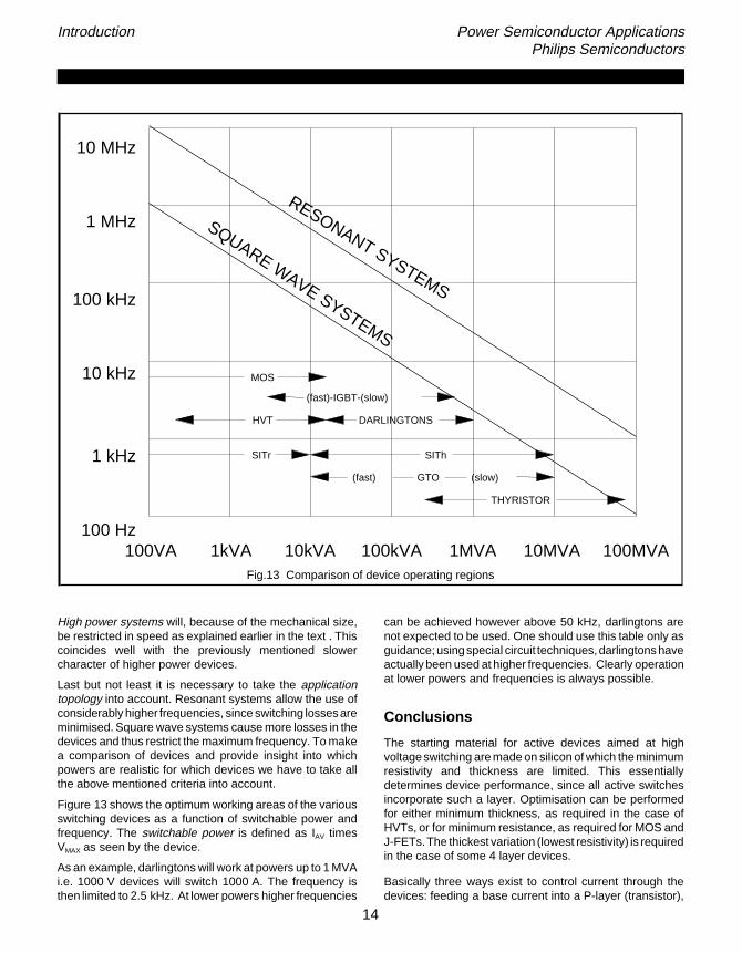
Fig.13 Comparison of device operating regions
10 MHz
1 MHz
100 kHz
10 kHz
1 kHz
100 Hz100VA 1kVA 10kVA 100kVA 1MVA 10MVA 100MVA
DARLINGTONSHVT
RESONANT SYSTEMS
SQUARE WAVE SYSTEMS
THYRISTOR
(fast)
(fast)-IGBT-(slow)
SITr SITh
MOS
GTO (slow)
High power systems will, because of the mechanical size,be restricted in speed as explained earlier in the text . Thiscoincides well with the previously mentioned slowercharacter of higher power devices.
Last but not least it is necessary to take the applicationtopology into account. Resonant systems allow the use ofconsiderably higher frequencies, since switching lossesareminimised. Square wave systems cause more losses in thedevices and thus restrict the maximum frequency. To makea comparison of devices and provide insight into whichpowers are realistic for which devices we have to take allthe above mentioned criteria into account.
Figure 13 shows the optimum working areas of the variousswitching devices as a function of switchable power andfrequency. The switchable power is defined as IAV timesVMAX as seen by the device.
As an example, darlingtons will work at powers up to 1 MVAi.e. 1000 V devices will switch 1000 A. The frequency isthen limited to 2.5 kHz. At lower powers higher frequencies
can be achieved however above 50 kHz, darlingtons arenot expected to be used. One should use this table only asguidance;usingspecial circuit techniques,darlingtons haveactually been used at higher frequencies. Clearly operationat lower powers and frequencies is always possible.
Conclusions
The starting material for active devices aimed at highvoltageswitching are made on silicon of which the minimumresistivity and thickness are limited. This essentiallydetermines device performance, since all active switchesincorporate such a layer. Optimisation can be performedfor either minimum thickness, as required in the case ofHVTs, or for minimum resistance, as required for MOS andJ-FETs.The thickest variation (lowest resistivity) is requiredin the case of some 4 layer devices.
Basically three ways exist to control current through thedevices: feeding a base current into a P-layer (transistor),
14
Introduction Power Semiconductor ApplicationsPhilips Semiconductors
using a voltage to pinch-off the current through openingsin the P-layer (J-FET) and by applying a voltage onto a gatewhich inverts the underlying P-layer (MOS).
The HVT is severely limited in operating frequency due toits stored hole charge, but this at the same time allows agreater current density and a lower on-state voltage. It alsorequires more drive energy than both MOS and J-FET.
When we add a P+-layer at the back of the three basic threelayer devices we make three basic four layer devices. TheP+-layer produces a PNP transistor at the back whichexhibits hole storage. This leads to much improved currentdensities and lower on-state losses, at the cost of switchingspeed. The four layer devices can be optimised for lowon-state losses, in which case the switching will be poor,or for fast switching, in which case the on-state voltage will
be high.
The properties of all six derived basic devices aredetermined to a large extent by the design of the highresistive area and can be optimised by applyingtechnological features in the devices such as lifetime killingand fine geometries.
Resonant systems allow devices to be used at much higherfrequencies due to the lower switching losses and theminimum on-times which may be longer, compared tosquare wave switching systems. Figure 13 gives theexpected maximum frequency and switching power for thediscussed devices. Thedifference for square wavesystemsand resonant systems is about a factor of 10.
15


Introduction Power Semiconductor ApplicationsPhilips Semiconductors
Power MOSFET
17


Introduction Power Semiconductor ApplicationsPhilips Semiconductors
1.2.1 PowerMOS Introduction
Device structure and fabricationThe idea of a vertical channel MOSFET has been knownsince the 1930s but it was not until the mid 1970s that thetechnology of diffusion, ion implantation and materialtreatment had reached the level necessary to produceDMOS on a commercial scale. The vertical diffusiontechnique uses technology more commonly associatedwith the manufacture of large scale integrated circuits thanwith traditional power devices. Figure 1(a) shows thevertical double implanted (DIMOS) channel structure whichis the basis for all Philips power MOSFET devices.
An N-channel PowerMOS transistor is fabricated on anN+substrate with a drain metallization applied to its’underside. Above the N+substrate is an N- epi layer, thethickness and resistivity of which depends on the requireddrain-source breakdown voltage. The channel structure,formed from a double implant in to the surface epi material,is laid down in a cellular pattern such that many thousandsof cells go to make a single transistor. The N+polysilicongate which is embedded in an isolating silicon dioxide layer,is a single structure which runs between the cells acrossthe entire active region of the device. The sourcemetallization also covers the entire structure and thus
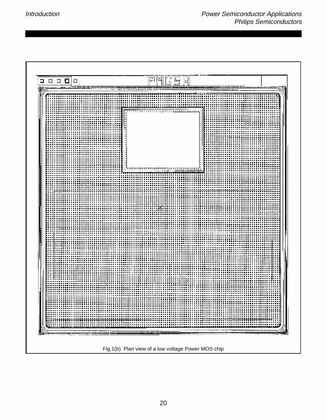
parallels all the individual transistor cells on the chip. Thelayout of a typical low voltage chip is shown in Fig.1(b). Thepolysilicon gate is contacted by bonding to the defined padarea while the source wires are bonded directly to thealuminium over the cell array. The back of the chip ismetallized with a triple layer of titanium/nickel/silver and thisenables the drain connection to be formed using a standardalloy bond process.
The active part of the device consists of many cellsconnected in parallel to give a high current handlingcapability where the current flow is vertical through the chip.Cell density is determined by photolithographic tolerancerequirements in defining windows in the polysilicon andgate-source oxide and also by the width of the polysilicontrack between adjacent cells. The optimum value forpolysilicon track width and hence cell density varies as afunction of device drain-source voltage rating, this isexplained in more detail further in the section. Typical celldensitiesare 1.6 million cells per square inch for low voltagetypes and 350,000 cells per square inch for high voltagetypes. The cell array is surrounded by an edge terminationstructure to control the surface electric field distribution inthe device off-state.
Fig.1(a) Power MOSFET cell structure.
19
Introduction Power Semiconductor ApplicationsPhilips Semiconductors
Fig.1(b) Plan view of a low voltage Power MOS chip
20

Introduction Power Semiconductor ApplicationsPhilips Semiconductors
A cross-section through a single cell of the array is shownin Fig.2. The channel length is approximately 1.5 micronsand is defined by the difference in the sideways diffusionof the N+ source and the P-body. Both these diffusions areauto-aligned to the edge of the polysilicon gate during thefabrication process. All diffusions are formed by ionimplantation followed by high temperature anneal/drive-into give good parameter reproducibility. The gate iselectrically isolated from the silicon by an 800 Angstromlayer of gate oxide (for standard types, 500 Angstrom forLogic level and from the overlying aluminium by a thick layerof phosphorus doped oxide. Windows are defined in thelatter oxide layer to enable the aluminium layer to contactthe N+ source and the P+ diffusion in the centre of each cell.The P+ diffusion provides a low resistance connectionbetween the P- body and ground potential, thus inhibitingturn-on of the inherent parasitic NPN bipolar structure.
Fig.2 Cross-section of a single cell.
Device operationCurrent flow in an enhancement mode power MOSFET iscontrolled by the voltage applied between the gate andsource terminals. The P- body isolates the source and drainregions and forms two P-N junctions connectedback-to-back. With both the gate and source at zero voltsthere is no source-drain current flow and the drain sits atthe positive supply voltage. The only current which can flowfrom source to drain is the reverse leakage current.
As the gate voltage is gradually made more positive withrespect to the source, holes are repelled and a depletedregion of silicon is formed in the P- body below thesilicon-gate oxide interface. The silicon is now in a’depleted’ state, but there is still no significant current flowbetween the source and drain.
When the gate voltage is further increased a very thin layerof electrons is formed at the interface between the P- bodyand the gate oxide. This conductive N-type channelenhanced by the positive gate-source voltage, now permitscurrent to flow from drain to source. The silicon in the P-
body is referred to as being in an ’inverted’ state. A slightincrease in gate voltage will result in a very significantincrease in drain current and a corresponding rapiddecrease in drain voltage, assuming a normal resistive loadis present.
Eventually the drain current will be limited by the combinedresistances of the load resistor and the RDS(ON) of theMOSFET. The MOSFET resistance reaches a minimumwhen VGS = +10 volts (assuming a standard type).Subsequently reducing the gate voltage to zero voltsreverses the above sequence of events. There are nostored charge effects since power MOSFETS are majoritycarrier devices.
Power MOSFET parameters
Threshold voltageThe threshold voltage is normally measured by connectingthe gate to the drain and then determining the voltage whichmust be applied across the devices to achieve a draincurrent of 1.0 mA. This method is simple to implement andprovides a ready indication of the point at which channelinversion occurs in the device.
The P- body is formed by the implantation of boron throughthe tapered edge of the polysilicon followed by an annealand drive-in. The main factors controlling threshold voltageare gate oxide thickness and peak surface concentrationin the channel, which is determined by the P-body implantdose. To allow for slight process variation a window isusually defined which is 2.1 to 4.0 volts for standard typesand 1.0 to 2.0 volts for logic level types.
Positive charges in the gate oxide, for example due tosodium, can cause the threshold voltage to drift. Tominimise this effect it is essential that the gate oxide isgrown under ultra clean conditions. In addition thepolysilicon gate and phosphorus doped oxide layer providea good barrier to mobile ions such as sodium and thus helpto ensure good threshold voltage stability.
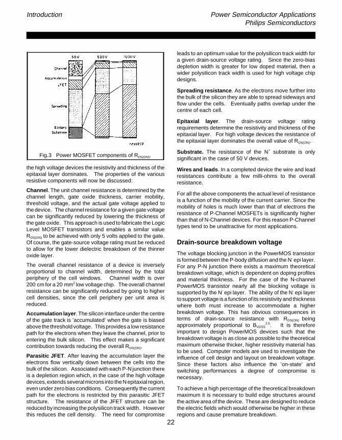
Drain-source on-state resistanceThe overall drain-source resistance, RDS(ON), of a powerMOSFET is composed of several elements, as shown inFig.3.
The relative contribution from each of the elements varieswith the drain-source voltage rating. For low voltagedevices the channel resistance is very important while for
N- EPI Layer
N+ Substrate
DRAIN
SOURCE
P- P-P+
N+ N+
GATE
20 um
21
Introduction Power Semiconductor ApplicationsPhilips Semiconductors
Fig.3 Power MOSFET components of RDS(ON).
the high voltage devices the resistivity and thickness of theepitaxial layer dominates. The properties of the variousresistive components will now be discussed:
Channel . The unit channel resistance is determined by thechannel length, gate oxide thickness, carrier mobility,threshold voltage, and the actual gate voltage applied tothe device. The channel resistance for a given gate voltagecan be significantly reduced by lowering the thickness ofthe gate oxide. This approach is used to fabricate the LogicLevel MOSFET transistors and enables a similar valueRDS(ON) to be achieved with only 5 volts applied to the gate.Of course, the gate-source voltage rating must be reducedto allow for the lower dielectric breakdown of the thinneroxide layer.
The overall channel resistance of a device is inverselyproportional to channel width, determined by the totalperiphery of the cell windows. Channel width is over200 cm for a 20 mm2 low voltage chip. The overall channelresistance can be significantly reduced by going to highercell densities, since the cell periphery per unit area isreduced.
Accumulation layer . The silicon interface under the centreof the gate track is ’accumulated’ when the gate is biasedabove the threshold voltage. Thisprovides a low resistancepath for the electrons when they leave the channel, prior toentering the bulk silicon. This effect makes a significantcontribution towards reducing the overall RDS(ON).
Parasitic JFET . After leaving the accumulation layer theelectrons flow vertically down between the cells into thebulk of the silicon. Associated with each P-N junction thereis a depletion region which, in the case of the high voltagedevices,extends severalmicrons into the N epitaxial region,even under zero bias conditions. Consequently the currentpath for the electrons is restricted by this parasitic JFETstructure. The resistance of the JFET structure can bereduced by increasing the polysilicon track width. Howeverthis reduces the cell density. The need for compromise
leads to an optimum value for the polysilicon track width fora given drain-source voltage rating. Since the zero-biasdepletion width is greater for low doped material, then awider polysilicon track width is used for high voltage chipdesigns.
Spreading resistance . As the electrons move further intothe bulk of the silicon they are able to spread sideways andflow under the cells. Eventually paths overlap under thecentre of each cell.
Epitaxial layer . The drain-source voltage ratingrequirements determine the resistivity and thickness of theepitaxial layer. For high voltage devices the resistance ofthe epitaxial layer dominates the overall value of RDS(ON).
Substrate. The resistance of the N+ substrate is onlysignificant in the case of 50 V devices.
Wires and leads . In a completed device the wire and leadresistances contribute a few milli-ohms to the overallresistance.
For all the above components the actual level of resistanceis a function of the mobility of the current carrier. Since themobility of holes is much lower than that of electrons theresistance of P-Channel MOSFETs is significantly higherthan that of N-Channel devices. For this reason P-Channeltypes tend to be unattractive for most applications.
Drain-source breakdown voltage
The voltage blocking junction in the PowerMOS transistoris formed between the P-body diffusion and the N- epi layer.For any P-N junction there exists a maximum theoreticalbreakdown voltage, which is dependent on doping profilesand material thickness. For the case of the N-channelPowerMOS transistor nearly all the blocking voltage issupported by the N- epi layer. The ability of the N- epi layertosupport voltage is a function of its resistivity and thicknesswhere both must increase to accommodate a higherbreakdown voltage. This has obvious consequences interms of drain-source resistance with RDS(ON) beingapproximately proportional to BVDSS
2.5. It is thereforeimportant to design PowerMOS devices such that thebreakdown voltage is as close as possible to the theoreticalmaximum otherwise thicker, higher resistivity material hasto be used. Computer models are used to investigate theinfluence of cell design and layout on breakdown voltage.Since these factors also influence the ’on-state’ andswitching performances a degree of compromise isnecessary.
To achieve a high percentage of the theoretical breakdownmaximum it is necessary to build edge structures aroundthe active area of the device. These are designed to reducethe electric fields which would otherwise be higher in theseregions and cause premature breakdown.
22

Introduction Power Semiconductor ApplicationsPhilips Semiconductors
For low voltage devices this structure consists of a fieldplate design, Fig.4. The plates reduce the electric fieldintensity at the corner of the P+ guard ring which surroundsthe active cell area, and spread the field laterally along thesurface of the device. The polysilicon gate is extended toform the first field plate, whilst the aluminium sourcemetallization forms the second plate. The polysilicontermination plate which is shorted to the drain in the cornersof the chip (not shown on the diagram) operates as achannel stopper. This prevents any accumulation ofpositive charge at the surface of the epi layer and thusimproves stability. Aluminium overlaps the terminationplate and provides a complete electrostatic screen againstany external ionic charges, hence ensuring good stabilityof blocking performance.
Fig.4 Field plate structure for low voltage devices.
For high voltage devices a set of floating P+ rings, see Fig.5,is used to control the electric field distribution around thedevice periphery. The number of rings in the structuredepends on the voltage rating of the device, eight rings areused for a 1000 volt type such as the BUK456-1000A. Athree dimensional computer model enables the optimumringspacing to be determined so that each ring experiencesa similar field intensity as the structure approachesavalanche breakdown. The rings are passivated withpolydox which acts as an electrostatic screen and preventsexternal ionic charges inverting the lightly doped N-
interface to form P- channels between the rings. Thepolydox is coated with layers of silicon nitride andphosphorus doped oxide.
All types have a final passivation layer of plasma nitride,which acts as a further barrier to mobile charge and alsogives anti-scratch protection to the top surface.
Fig.5 Ring structure for high voltage devices.
Electrical characteristics
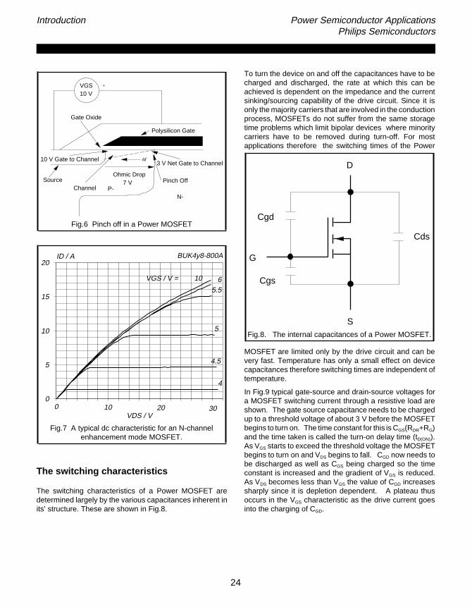
The DC characteristicIf a dc voltage source is connected across the drain andsource terminals of an N channel enhancement modeMOSFET, with the positive terminal connected to the drain,the following characteristics can be observed. With the gateto source voltage held below the threshold level negligiblecurrent will flow when sweeping the drain source voltagepositive from zero. If the gate to source voltage is takenabove the threshold level, increasing the drain to sourcevoltage will cause current to flow in the drain. This currentwill increase as the drain-source voltage is increased up toa point known as the pinch off voltage. Increasing thedrain-source terminal voltage above this value will notproduce any significant increase in drain current.
The pinch off voltage arises from a rapid increase inresistance which for any particular MOSFET will dependon the combination of gate voltage and drain current. In itssimplest form, pinch off will occur when the ohmic dropacross the channel region directly beneath the gatebecomes comparable to the gate to source voltage. Anyfurther increase in drain current would now reduce the netvoltage across the gate oxide to a level which is no longersufficient to induce a channel. The channel is thus pinchedoff at its edge furthest from the source N+ (see Fig.6).
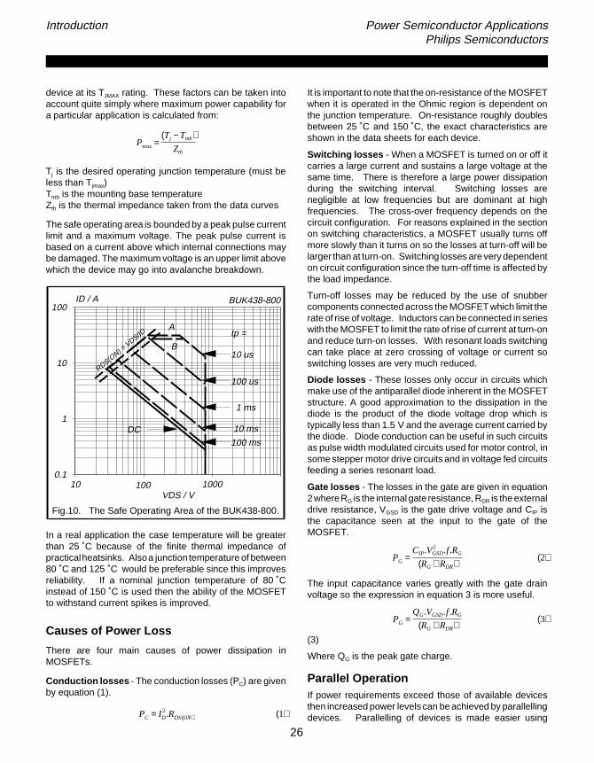
A typical set of output characteristics is shown in Fig.7. Thetwo regions of operation either side of the pinch off voltagecan be seen clearly. The region at voltages lower than thepinch off value is usually known as the ohmic region.Saturation region is the term used to describe that part ofthe characteristic above the pinch-off voltage. (NB Thisdefinition of saturation is different to that used for bipolardevices.)
N- EPI Layer
P+
N+
P-
LOPOX
LPCVD NITRIDE
POLYDOX
P+P+P+P+
SourceGuardRing
Floating Guard Rings
N- EPI Layer
N+ Substrate
P+
P-
N+
Guard Ring
Polysilicon
SourceMetallization
Gate RingSource RingPolysiliconTerminationPlate
(Source)
23
Introduction Power Semiconductor ApplicationsPhilips Semiconductors
Fig.6 Pinch off in a Power MOSFET
Fig.7 A typical dc characteristic for an N-channelenhancement mode MOSFET.
The switching characteristics
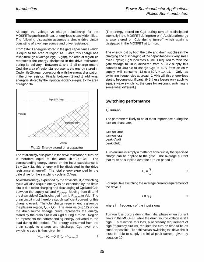
The switching characteristics of a Power MOSFET aredetermined largely by the various capacitances inherent inits’ structure. These are shown in Fig.8.
To turn the device on and off the capacitances have to becharged and discharged, the rate at which this can beachieved is dependent on the impedance and the currentsinking/sourcing capability of the drive circuit. Since it isonly the majority carriers that are involved in the conductionprocess, MOSFETs do not suffer from the same storagetime problems which limit bipolar devices where minoritycarriers have to be removed during turn-off. For mostapplications therefore the switching times of the Power
Fig.8. The internal capacitances of a Power MOSFET.
MOSFET are limited only by the drive circuit and can bevery fast. Temperature has only a small effect on devicecapacitances therefore switching times are independent oftemperature.
In Fig.9 typical gate-source and drain-source voltages fora MOSFET switching current through a resistive load areshown. The gate source capacitance needs to be chargedup to a threshold voltage of about 3 V before the MOSFETbegins to turn on. The time constant for this is CGS(RDR+RG)and the time taken is called the turn-on delay time (tD(ON)).As VGS starts to exceed the threshold voltage the MOSFETbegins to turn on and VDS begins to fall. CGD now needs tobe discharged as well as CGS being charged so the timeconstant is increased and the gradient of VGS is reduced.As VDS becomes less than VGS the value of CGD increasessharply since it is depletion dependent. A plateau thusoccurs in the VGS characteristic as the drive current goesinto the charging of CGD.
VGS10 V
Ohmic Drop7 V
3 V Net Gate to Channel10 V Gate to Channel
Polysilicon Gate
Gate Oxide
P-Source
ChannelN-
Pinch Off
Id
+
D
S
G
Cgs
Cgd
Cds
0VDS / V
ID / A BUK4y8-800A20
15
10
5
0
4
5
6
4.5
5.5
10
10 20 30
VGS / V =
24

Introduction Power Semiconductor ApplicationsPhilips Semiconductors
Fig.9. The switching waveforms for a MOSFET.
0 0.2 0.4 0.6 0.8 1 1.2
50
40
30
20
10
0
Time (Microseconds)
Vol
tage
(V
olts
)
Drain-Source Voltage
Gate-Source Voltage
Turn-on Turn-off
When VDS has collapsed VGS continues to rise as overdriveis applied. Gate overdrive is necessary to reduce theon-resistance of the MOSFET and thereby keep power lossto a minimum.
To turn the MOSFET off the overdrive has first to beremoved. The charging path for CGD and CDS now containsthe load resistor (RL) and so the turn-off time will begenerally longer than the turn-on time.
The Safe Operating AreaUnlike bipolar devices Power MOSFETs do not suffer fromsecond breakdown phenomena when operated within theirvoltage rating. Essentially therefore the safe operating areaof a Power MOSFET is determined only by the power
necessary to raise its junction temperature to the ratedmaximum of 150 ˚C or 175 ˚C (which TJMAX depends onpackage and voltage rating). Whether a MOSFET is beingoperated safely with respect to thermal stress can thus bedetermined directly from knowledge of the power functionapplied and the thermal impedance characteristics.
Asafe operating areacalculated assumingamounting basetemperature of 25 ˚C is shown in Fig.10 for a BUK438-800device. This plot shows the constant power curves for avariety of pulse durations ranging from dc to 10 µs. Thesecurves represent the power levels which will raise Tj up tothe maximum rating. Clearly for mounting basetemperatures higher than 25 ˚C the safe operating area issmaller. In addition it is not usually desirable to operate the
25
Introduction Power Semiconductor ApplicationsPhilips Semiconductors
device at its TJMAX rating. These factors can be taken intoaccount quite simply where maximum power capability fora particular application is calculated from:
Tj is the desired operating junction temperature (must beless than Tjmax)Tmb is the mounting base temperatureZth is the thermal impedance taken from the data curves
The safe operating area is bounded by a peak pulse currentlimit and a maximum voltage. The peak pulse current isbased on a current above which internal connections maybe damaged. The maximum voltage is an upper limit abovewhich the device may go into avalanche breakdown.
Fig.10. The Safe Operating Area of the BUK438-800.
In a real application the case temperature will be greaterthan 25 ˚C because of the finite thermal impedance ofpracticalheatsinks. Alsoa junction temperature of between80 ˚C and 125 ˚C would be preferable since this improvesreliability. If a nominal junction temperature of 80 ˚Cinstead of 150 ˚C is used then the ability of the MOSFETto withstand current spikes is improved.
Causes of Power Loss
There are four main causes of power dissipation inMOSFETs.
Conduction losses - The conduction losses (PC) are givenby equation (1).
It is important to note that the on-resistance of the MOSFETwhen it is operated in the Ohmic region is dependent onthe junction temperature. On-resistance roughly doublesbetween 25 ˚C and 150 ˚C, the exact characteristics areshown in the data sheets for each device.
Switching losses - When a MOSFET is turned on or off itcarries a large current and sustains a large voltage at thesame time. There is therefore a large power dissipationduring the switching interval. Switching losses arenegligible at low frequencies but are dominant at highfrequencies. The cross-over frequency depends on thecircuit configuration. For reasons explained in the sectionon switching characteristics, a MOSFET usually turns offmore slowly than it turns on so the losses at turn-off will belarger than at turn-on. Switching losses are very dependenton circuit configuration since the turn-off time is affected bythe load impedance.
Turn-off losses may be reduced by the use of snubbercomponents connected across the MOSFET which limit therate of rise of voltage. Inductors can be connected in serieswith the MOSFET to limit the rate of rise of current at turn-onand reduce turn-on losses. With resonant loads switchingcan take place at zero crossing of voltage or current soswitching losses are very much reduced.
Diode losses - These losses only occur in circuits whichmake use of the antiparallel diode inherent in the MOSFETstructure. A good approximation to the dissipation in thediode is the product of the diode voltage drop which istypically less than 1.5 V and the average current carried bythe diode. Diode conduction can be useful in such circuitsas pulse width modulated circuits used for motor control, insome stepper motor drive circuits and in voltage fed circuitsfeeding a series resonant load.
Gate losses - The losses in the gate are given in equation2whereRG is the internal gate resistance, RDR is the externaldrive resistance, VGSD is the gate drive voltage and CIP isthe capacitance seen at the input to the gate of theMOSFET.
The input capacitance varies greatly with the gate drainvoltage so the expression in equation 3 is more useful.
(3)
Where QG is the peak gate charge.
Parallel OperationIf power requirements exceed those of available devicesthen increased power levels can be achieved by parallellingdevices. Parallelling of devices is made easier using
Pmax =(Tj − Tmb)
Zth
10 1000VDS / V
ID / A100
10
1
0.1
100 us
1 ms
10 ms
RDS(ON) =
VDS/ID
100 ms DC
10 us
tp =
BUK438-800
100
A
B
PG =CIP.VGSD
2 .f .RG
(RG + RDR)(2)
PG =QG.VGSD.f .RG
(RG + RDR)(3)
PC = ID2.RDS(ON) (1)
26

Introduction Power Semiconductor ApplicationsPhilips Semiconductors
MOSFETs because they have a positive temperaturecoefficient of resistance. If one parallelled MOSFET carriesmore current than the others it becomes hotter. Thiscauses the on-resistance of that particular device tobecome greater than that of the others and so the currentin it reduces. This mechanism opposes thermal runawayin one of the devices. The positive temperature coefficientalso helps to prevent hot spots within the MOSFET itself.
Applications of Power MOSFETsPower MOSFETs are ideally suited for use in manyapplications, some of which are listed below. Furtherinformation on the major applications is presented in
subsequent chapters.
Chapter 2: Switched mode power supplies (SMPS)
Chapter 3: Variable speed motor control.
Chapter 5: Automotive switching applications.
ConclusionsIt can be seen that the operation of the Power MOSFET isrelatively easy to understand. The advantages of fastswitching times, ease of parallelling and low drive powerrequirements make the device attractive for use in manyapplications.
27


Introduction Power Semiconductor ApplicationsPhilips Semiconductors
1.2.2 Understanding Power MOSFET Switching Behaviour
Power MOSFETs are well known for their ease of drive andfast switching behaviour. Being majority carrier devicesmeans they are free of the charge storage effects whichinhibit the switching performance of bipolar products. Howfast a Power MOSFET will switch is determined by thespeed at which its internal capacitances can be chargedand discharged by the drive circuit. MOSFET switchingtimes are often quoted as part of the device data howeveras an indication as to the true switching capability of thedevice, these figures are largely irrelevant. The quotedvalues are only a snapshot showing what will be achievedunder the stated conditions.
This report sets out to explain the switching characteristicsof Power MOSFETs. It will consider the main features ofthe switching cycle distinguishing between what is devicedeterminant and what can be controlled by the drive circuit.The requirements for the drive circuit are discussed in termsof the energy that it must supply as well as the currents itis required to deliver. Finally, how the drive circuitinfluences switching performance, in terms of switchingtimes, dV/dt and dI/dt will be reviewed.
Voltage dependent capacitanceThe switching characteristics of the Power MOSFET aredetermined by its capacitances. These capacitances arenot fixed but are a function of the relative voltages betweeneach of the terminals. To fully appreciate Power MOSFETswitching, it is necessary to understand what gives rise tothis voltage dependency.
Parallel plate capacitance is expressed by the well knownequation
where ’a’ is the area of the plates, d is the separatingdistance and Ε is the permittivity of the insulating materialbetween them. For a parallel plate capacitor, the plates aresurfaces on which charge accumulation / depletion occursin response to a change in the voltage applied across them.In a semiconductor, static charge accumulation / depletioncan occur either across a PN junction or at semiconductorinterfaces either side of a separating oxide layer.
i) P-N junction capacitanceThe voltage supporting capability of most powersemiconductors is provided by a reverse biased P-Njunction. The voltage is supported either side of the junctionby a region of charge which is exposed by the appliedvoltage. (Usually referred to as the depletion regionbecause it is depleted of majority carriers.) Fig.1 showshow the electric field varies across a typical P-N- junction
for a fixed dc voltage. The shaded area beneath the curvemust be equal to the applied voltage. The electric fieldgradient is fixed, independent of the applied voltage,according to the concentration of exposed charge. (This isequal to the background doping concentration used duringdevice manufacture.) A slight increase in voltage abovethis dc level will require an extensionof the depletion region,and hence more charge to be exposed at its edges, this isillustrated in Fig.1. Conversely a slight reduction in voltagewill cause the depletion region to contract with a removalof exposed charge at its edge. Superimposing a small acsignal on the dc voltage thus causes charge to be addedand subtracted at either side of the depletion region of widthd1. The effective capacitance per unit area is
Since the depletion region width is voltage dependent it canbe seen from Fig.1 that if the dc bias is raised to say V2,the junction capacitance becomes
Junction capacitance is thus dependent on applied voltagewith an inverse relationship.
Fig.1 Voltage dependence of a PN junctioncapacitance
ii) Oxide capacitanceFig.2 shows two semiconductor layers separated by aninsulating oxide. In this case the surface layer is polysilicon(representative of the PowerMOS gate structure) and thelower layer is a P-type substrate. Applying a negativevoltage to the upper layer with respect to the lower will causepositive charge accumulation at the surface of the P-doped
C1 =Εd1
2
C2 =Εd2
3
E
xd1d2
V1
V2
N type siliconP type silicon
C = Εad
1
29

Introduction Power Semiconductor ApplicationsPhilips Semiconductors
material (positively charged holes of the P material areattracted by the negative voltage). Any changes in thisapplied voltage will cause a corresponding change in theaccumulation layer charge. The capacitance per unit areais thus
where t = oxide thickness
Applying a positive voltage to the gate will cause a depletionlayer to form beneath the oxide, (ie the positively chargedholes of the P-material are repelled by the positive voltage).The capacitance will now decrease with increasing positivegate voltage as a result of widening of the depletion layer.Increasing the voltage beyond a certain point results in aprocess known as inversion; electrons pulled into theconduction band by the electric field accumulate at thesurface of the P-type semiconductor. (The voltage at whichthis occurs is the threshold voltage of the power MOSFET.)Once the inversion layer forms, the depletion layer widthwill not increase with additional dc bias and the capacitanceis thus at its minimum value. (NB the electron chargeaccumulation at the inversion layer cannot follow a highfrequency ac signal in the structure of Fig.2, so highfrequency capacitance is still determined by the depletionlayer width.) The solid line of Fig.3 represents thecapacitance-voltage characteristic of an MOS capacitor.
Fig.2 Oxide capacitance
In a power MOSFET the solid line is not actually observed;the formation of the inversion layer in the P-type materialallows electrons to move from the neighbouring N+-source,the inversion layer can therefore respond to a highfrequency gate signal and the capacitance returns to itsmaximum value, dashed line of Fig.3.
Fig.3 C-V plot for MOS capacitance
Power MOSFET capacitances
Fig.4 Parasitic capacitance model
The circuit model of Fig.4 illustrates the parasiticcapacitances of the Power MOSFET. Most PowerMOSdata sheets do not refer to these components but to inputcapacitance Ciss, output capacitance Coss and feedbackcapacitance Crss. The data sheet capacitances relate tothe primary parasitic capacitances of Fig.4 as follows:
Ciss: Parallel combination of Cgs and CgdCoss: Parallel combination of Cds and CgdCrss: Equivalent to Cgd
Fig.5 shows the cross section of a power MOSFET cellindicatingwhere the parasiticcapacitances occur internally.
Cox
C
Bias Voltage
(Polysilicon to P-type silicon)
Cox =Εt
4
Cgd
Cds
Cgs
G
S
D
toxide
P type silicon
Polysilicon
30

Introduction Power Semiconductor ApplicationsPhilips Semiconductors
Fig.5 Cross section of a single PowerMOS cell showinginternal capacitance
Thecapacitancebetween drain andsource is aP-N junctioncapacitance, varying in accordance with the width of thedepletion layer, which in turn depends on the voltage beingsupported by the device. The gate source capacitanceconsists of the three components, CgsN+, CgsP and CgsM.Of these CgsP is across the oxide which will vary accordingto the applied gate source voltage as described above.
Of particular interest is the feedback capacitance Cgd. Itis this capacitance which plays a dominant role duringswitching and which is also the most voltage dependent.Cgd is essentially two capacitors in series such that
CgsN+
CgsM OxidePolysilicon
N+P-
P
N-
N+
MetalizationSource
Drain
Gate
Cgdbulk
CgdoxCgsP
Cds Depletion Layer
1Cgd
=1
Cgdox+
1Cgdbulk
5
Fig.6 How Cgd is affected by voltage
OxidePolysilicon
N+P-
P
N-
N+
Metalization
Source
Drain
Gate
Depletion Layer Widths
Area of Oxide Capacitance Exposedfor Voltages V1 & V2
For Three Applied Voltages
Width for Cgdbulk
at Voltage V3
V3
V2V1
31

Introduction Power Semiconductor ApplicationsPhilips Semiconductors
Fig.6 illustrateshow this capacitance is affected by the drainto gate voltage. With a large voltage drain to gate, Cgdbulkis very small due to the wide depletion region and thusmaintains Cgd at a low value. As the voltage is reducedthe depletion region shrinks until eventually the oxidesemiconductor interface is exposed. This occurs as Vdgapproaches 0 V. Cgdox now dominates Cgd. As Vdg isfurther reduced the drain will become negative with respectto the gate (normal on-state condition) an increasing areaof the oxide-semiconductor interface is exposed and anaccumulation layer forms at the semiconductor surface.Thenow large area of exposed oxide results in a large valuefor Cgdox and hence Cgd. Fig.7 shows Cgd plotted as afunction of drain to gate voltage. This illustrates the almoststep increase in capacitance at the point where Vgs = Vgd.
Fig.7 How Cgd varies with drain to gate voltage
Charging cycle - The Gate ChargeOscillogramThe switching cycle of a power MOSFET can be clearlyobserved by applying a constant current to the gate andusing a constant current source as the load, Fig.8. In thiscircuit the MOSFET is turned on by feeding a constantcurrent of 1 mA on to the gate, conversely the device isturned off by extracting a constant current of 1 mA from thegate. The gate and drain voltages with respect to sourcecan be monitored on an oscilloscope as a function of time.Since Q = it, a 1 µsec period equates to 1 nc of chargeapplied to the gate. The gate source voltage can thus beplotted as a function of charge on the gate. Fig.9 showssuch a plot for the turn-on of a BUK555-100A, also shownis the drain to source voltage. This gate voltage plot showsthe characteristic shape which results from charging of thepower MOSFETs input capacitance. This shape arises asfollows: (NB the following analysis uses the two circuitmodels of Fig.10 to represent a MOSFET operating in theactive region (a) and the ohmic region (b). In the active
region the MOSFET is a constant current source where thecurrent is a function of the gate-source voltage. In the ohmicregion the MOSFET is in effect just a resistance.)
Fig.8 Gate charge circuit
At time, t0 (Fig.9), the gate drive is activated. Current flowsinto the gate as indicated in Fig.11(a), charging both Cgsand Cgd. After a short period the threshold voltage isreached and current begins to rise in the MOSFET. Theequivalent circuit is now as shown in Fig.11(b). The drainsource voltage remains at the supply level as long as id < I0and the free wheeling diode D is conducting.
Fig.9 Gate charge plot for a BUK555-100A (Logic LevelFET)
Vdd
Vdg0
Cdg
0 10 20 30 40
26
24
22
20
18
16
14
12
10
8
6
4
2
0
(V)
(us)(1us = 1 nc for Vgs plot)
Vds
Vgs
BUK555-100A(@ Id = 25 A)
t0 t1 t2
32

Introduction Power Semiconductor ApplicationsPhilips Semiconductors
The current in the MOSFET continues to rise until id = I0,since the device is still in its active region, the gate voltagebecomes clamped at this point, (t1). The entire gate currentnow flows through Cgd causing the drain-source voltage todrop as Cgd is discharged, Fig.11(c). The rate at whichVds falls is given by:
As Vdg approaches zero, Cgd starts to increasedramatically, reaching its maximum as Vdg becomesnegative. dVds/dt is now greatly reduced giving rise to thevoltage tail.
Once the drain-source voltage has completed its drop tothe on-state value of I0.RDS(ON), (point t2), the gate sourcevoltage becomes unclamped and continues to rise,Fig.11(d). (NB dVgs/dQ in regions 1 and 3 indicates the
input capacitance values.)
Fig.10 Equivalent circuits for a Power MOSFET duringswitching
G
D
S
Cgd
Cgs
id = f(Vgs)
G
D
S
Cgd
Cgs
Rds(on)
(a) (b)
dVdsdt
=dVdg
dt=
igCgd
6
Fig.11 Charging the parasitic capacitance during turn-on
Vdd
Cgd
Cgs
Io
(a) Vdd
Cgd
Cgs
id = f(Vgs)
Io
(b)
Vdd
Cgd
Cgs
id = f(Vgs)
Io
(c) Vdd
Cgd
Cgs
Rds(on)
Io
(d)
33

Introduction Power Semiconductor ApplicationsPhilips Semiconductors
The gate charge oscillogram can be found in the data forall Philips PowerMOS devices. This plot can be used todetermine the required average gate drive current for aparticular switching speed. The speed is set by how fastthe charge is supplied to the MOSFET.
Energy consumed by the switching eventIn the majority of applications the power MOSFET will bedriven not from a constant current source but via a fixed
gate drive impedance from a voltage source. Fig.13 showsthe voltageon avoltage independentcapacitor as a functionof charge. The area beneath the charge vs voltage curveequals the stored energy (E = Q.V/2). The area above thecharge vs voltage curve (bounded by the supply voltage)is the amount of energy dissipated during the charging cyclefrom a fixed voltage source. The total energy delivered bythe supply is therefore Q.V, where 1/2 Q.V is stored on thecapacitor to be dissipated during the discharge phase.
Fig.12 Gate charging cycle
t0 t1 t2 t3 t4 t5 t6
1a 2a 3a
1b 2b3b
4a
4b
Vgg
Vdd
Out
put C
apac
itanc
e
34
Introduction Power Semiconductor ApplicationsPhilips Semiconductors
Although the voltage vs charge relationship for theMOSFETs gate is not linear, energy loss is easily identified.The following discussion assumes a simple drive circuitconsisting of a voltage source and drive resistance.
From t0 to t1 energy is stored in the gate capacitance whichis equal to the area of region 1a. Since this charge hasfallen through a voltage Vgg - Vgs(t), the area of region 1brepresents the energy dissipated in the drive resistanceduring its delivery. Between t1 and t2 all charge entersCgd, the area of region 2a represents the energy stored inCgd while 2b again corresponds with the energy dissipationin the drive resistor. Finally, between t2 and t3 additionalenergy is stored by the input capacitance equal to the areaof region 3a.
Fig.13 Energy stored on a capacitor
The total energy dissipated in the drive resistance at turn-onis therefore equal to the area 1b + 2b + 3b. Thecorresponding energy stored on the input capacitance is1a + 2a + 3a, this energy will be dissipated in the driveresistance at turn-off. The total energy expended by thegate drive for the switching cycle is Q.Vgg.
As well as energy expended by the drive circuit, a switchingcycle will also require energy to be expended by the draincircuit due to the charging and discharging of Cgd and Cdsbetween the supply rail and VDS(ON). Moving from t5 to t6the drain side of Cgd is charged from Io.RDS(ON) to Vdd. Thedrain circuit must therefore supply sufficient current for thischarging event. The total charge requirement is given bythe plateau region, Q6 - Q5. The area 4a (Fig.12) underthe drain-source voltage curve represents the energystored by the drain circuit on Cgd during turn-on. Region4b represents the corresponding energy delivered to theload during this period. The energy consumed from thedrain supply to charge and discharge Cgd over oneswitching cycle is thus given by:
(The energy stored on Cgd during turn-off is dissipatedinternally in the MOSFET during turn-on.) Additional energyis also stored on Cds during turn-off which again isdissipated in the MOSFET at turn-on.
The energy lost by both the gate and drain supplies in thecharging and discharging of the capacitances is very smallover 1 cycle; Fig.9 indicates 40 nc is required to raise thegate voltage to 10 V, delivered from a 10 V supply thisequates to 400 nJ; to charge Cgd to 80 V from an 80 Vsupply will consume 12 nc x 80 V = 1.4 µJ. Only asswitching frequencies approach 1 MHz will this energy lossstart to become significant. (NB these losses only apply tosquare wave switching, the case for resonant switching issome-what different.)
Switching performance
1) Turn-on
The parameters likely to be of most importance during theturn-on phase are,
turn-on timeturn-on losspeak dV/dtpeak dI/dt.
Turn-on time is simply a matter of how quickly the specifiedcharge can be applied to the gate. The average currentthat must be supplied over the turn-on period is
For repetitive switching the average current requirement ofthe drive is
where f = frequency of the input signal
Turn-on loss occurs during the initial phase when currentflows in the MOSFET while the drain source voltage is stillhigh. To minimise this loss, a necessary requirement ofhigh frequency circuits, requires the turn-on time to be assmall as possible. To achieve fast switching the drive circuitmust be able to supply the initial peak current, given byequation 10.
Voltage
Charge
Stored Energy
Supply Voltage
Ion =Qton
8
I = Q.f 9
WDD = (Q6 − Q5).(VDD − VDS(ON)) 7
35
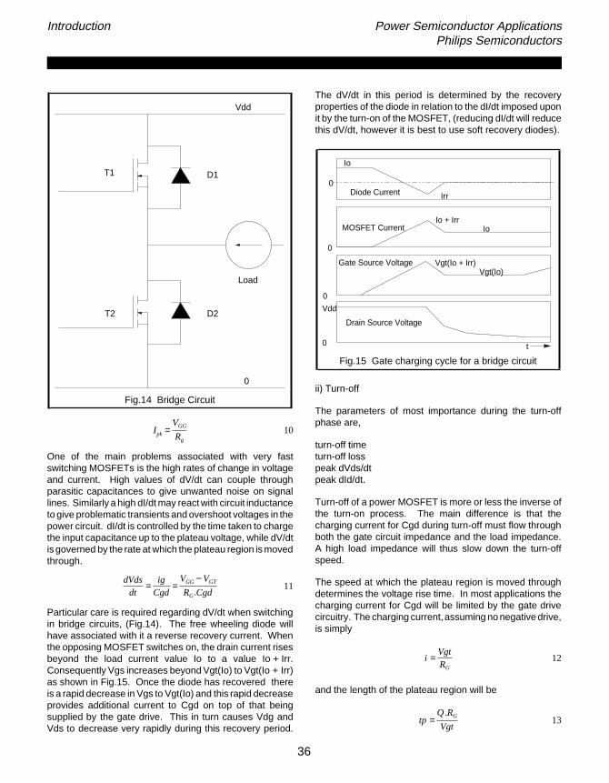
Introduction Power Semiconductor ApplicationsPhilips Semiconductors
Fig.14 Bridge Circuit
One of the main problems associated with very fastswitching MOSFETs is the high rates of change in voltageand current. High values of dV/dt can couple throughparasitic capacitances to give unwanted noise on signallines. Similarly a high dI/dt may react with circuit inductanceto give problematic transients and overshoot voltages in thepower circuit. dI/dt is controlled by the time taken to chargethe input capacitance up to the plateau voltage, while dV/dtis governed by the rate at which the plateau region is movedthrough.
Particular care is required regarding dV/dt when switchingin bridge circuits, (Fig.14). The free wheeling diode willhave associated with it a reverse recovery current. Whenthe opposing MOSFET switches on, the drain current risesbeyond the load current value Io to a value Io + Irr.Consequently Vgs increases beyond Vgt(Io) to Vgt(Io + Irr)as shown in Fig.15. Once the diode has recovered thereis a rapid decrease in Vgs to Vgt(Io) and this rapid decreaseprovides additional current to Cgd on top of that beingsupplied by the gate drive. This in turn causes Vdg andVds to decrease very rapidly during this recovery period.
The dV/dt in this period is determined by the recoveryproperties of the diode in relation to the dI/dt imposed uponit by the turn-on of the MOSFET, (reducing dI/dt will reducethis dV/dt, however it is best to use soft recovery diodes).
Fig.15 Gate charging cycle for a bridge circuit
ii) Turn-off
The parameters of most importance during the turn-offphase are,
turn-off timeturn-off losspeak dVds/dtpeak dId/dt.
Turn-off of a power MOSFET is more or less the inverse ofthe turn-on process. The main difference is that thecharging current for Cgd during turn-off must flow throughboth the gate circuit impedance and the load impedance.A high load impedance will thus slow down the turn-offspeed.
The speed at which the plateau region is moved throughdetermines the voltage rise time. In most applications thecharging current for Cgd will be limited by the gate drivecircuitry. The charging current,assuming no negative drive,is simply
and the length of the plateau region will be
T1
T2
D1
D2
Load
Vdd
0
Vdd
0
0
Vgt(Io)Vgt(Io + Irr)Gate Source Voltage
Drain Source Voltage
MOSFET Current
0
IoIo + Irr
Diode Current0
Io
Irr
t
Ipk =VGG
Rg
10
dVdsdt
=ig
Cgd=
VGG − VGT
RG.Cgd11
i =VgtRG
12
tp =Q.RG
Vgt13
36

Introduction Power Semiconductor ApplicationsPhilips Semiconductors
The implications for low threshold (Logic Level) MOSFETsare clear from the above equations. The lower value of Vgtwill mean a slower turn-off for a given gate impedance whencompared to an equivalent standard threshold device.Equivalent switching therefore requires a lower driveimpedance to be used.
ConclusionsIn theory the speed of a power MOSFET is limited only bythe parasitic inductances of its internal bond wires. The
speed is essentially determined by how fast the internalcapacitances can be charged and discharged by the drivecircuit. Switching speeds quoted in data should be treatedwith caution since they only reflect performance for oneparticular drive condition. The gate charge plot is a moreuseful way of looking at switching capability since itindicates how much charge needs to be supplied by thedrive to turn the device on. How fast that charge should beapplied depends on the application and circuit performancerequirements.
37


Introduction Power Semiconductor ApplicationsPhilips Semiconductors
1.2.3 Power MOSFET Drive Circuits
MOSFETs are being increasingly used in many switchingapplications because of their fast switching times and lowdrive power requirements. The fast switching times caneasily be realised by driving MOSFETs with relativelysimple drive circuits. The following paragraphs outline therequirementsof MOSFET drive circuits and present variouscircuit examples. A look at the special requirements of veryfast switching circuits is also presented, this can be foundin the latter part of this article.
The requirements of the drive circuit
The switching of a MOSFET involves the charging anddischarging of the capacitance between the gate andsource terminals. This capacitance is related to the size ofthe MOSFET chip used typically about 1-2 nF. Agate-source voltage of 6V is usually sufficient to turn astandard MOSFET fully on. However further increases ingate-to-source voltage are usually employed to reduce theMOSFETs on-resistance. Therefore for switching times ofabout 50 ns, applying a 10 V gate drive voltage to aMOSFET with a 2 nF gate-source capacitance wouldrequire the drive circuit to sink and source peak currents ofabout 0.5 A. However it is only necessary to carry thiscurrent during the switching intervals.
The gate drive power requirements are given in equation(1)
where QG is the peak gate charge, VGS is the peak gatesource voltage and f is the switching frequency.
In circuits which use a bridge configuration, the gateterminals of the MOSFETs in the circuit need to float relativeto each other. The gate drive circuitry then needs toincorporatesome isolation.The impedance of the gatedrivecircuit should not be so large that there is a possibility ofdV/dt turn on. dV/dt turn on can be caused by rapid changesof drain to source voltage. The charging current for thegate-drain capacitance CGD flows through the gate drivecircuit. This charging current can cause a voltage dropacross the gate drive impedance large enough to turn theMOSFET on.
Non-isolated drive circuitsMOSFETs can be driven directly from a CMOS logic IC asshown in Fig.1.
Fig.1 A very simple drive circuit utilizing a standardCMOS IC
Faster switching speeds can be achieved by parallellingCMOS hex inverting (4049) or non-inverting (4050) buffersas shown in Fig.2.
Fig.2 Driving Philips PowerMOS with 6 parallelledbuffered inverters.
A push pull circuit can also be used as shown in Fig.3.
Theconnections between the drive circuit and the MOSFETshould be kept as short as possible and twisted together ifthe shortest switching times are required. If both the drivecircuit and the terminals of the MOSFET are on the samePCB, then the inductance of tracks, between the drivetransistors and the terminals of the MOSFETs, should bekept as small as possible. This is necessary to reduce theimpedance of the drive circuit in order to reduce theswitching times and lessen the susceptibility of the circuit
4011
4049
0 V
15 V
PG = QG.VGS.f 1
39

Introduction Power Semiconductor ApplicationsPhilips Semiconductors
Fig.3 A drive circuit using a two transistor push pullcircuit.
to dV/dt turn-on of the MOSFET. Attention to layout alsoimproves the immunity to spurious switching byinterference.
One of the advantages of MOSFETs is that their switchingtimes can be easily controlled. For example it may berequired to limit the rate of change of drain current to reduceovershoot on the drain source voltage waveform. Theovershoot may be caused by switching current in parasiticlead or transformer leakage inductance. The slowerswitching can be achieved by increasing the value of thegate drive resistor.
The supply rails should be decoupled near to fast switchingelements such as the push-pull transistors in Fig.3. Anelectrolytic capacitor in parallel with a ceramic capacitor arerecommended since the electrolytic capacitor will not be alow enough impedance to the fast edges of the MOSFETdrive pulse.
Isolated drive circuitsSome circuits demand that the gate and source terminalsof MOSFETs are floating with respect to those of otherMOSFETs in the circuit. Isolated drive to these MOSFETscan be provided in the following way:
(a) Opto-isolators.
A drive circuit using an opto-isolator is shown in Fig.4.
A diode in the primary side of the opto-isolator emitsphotons when it is forward biased. These photons impingeon the base region of a transistor in the secondary side.This causes photogeneration of carriers sufficient to satisfythe base requirement for turn-on. In this way theopto-isolator provides isolation between the primary andsecondary of the opto-isolator. An isolated supply isrequired for the circuitry on the secondary side of theopto-isolator. This supply can be derived, in some cases,from the drain-to-source voltage across the MOSFET beingdriven as shown in Fig.5. This is made possible by the lowdrive power requirements of MOSFETs.
Fig.4. An isolated drive circuit using an opto-isolator.
4049
0 V
15 V
Opto-Isolator
5 V
40
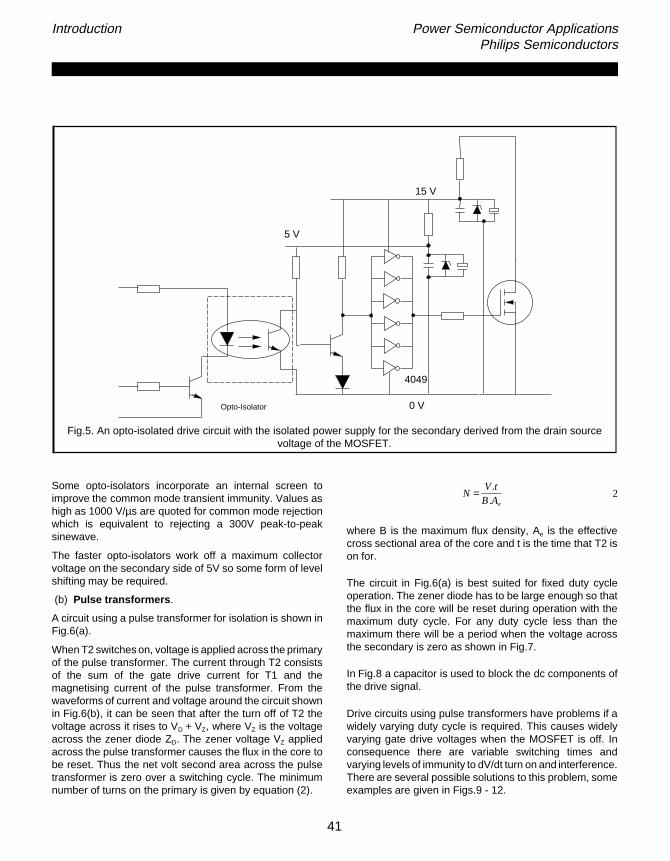
Introduction Power Semiconductor ApplicationsPhilips Semiconductors
Fig.5. An opto-isolated drive circuit with the isolated power supply for the secondary derived from the drain sourcevoltage of the MOSFET.
4049
0 V
15 V
Opto-Isolator
5 V
Some opto-isolators incorporate an internal screen toimprove the common mode transient immunity. Values ashigh as 1000 V/µs are quoted for common mode rejectionwhich is equivalent to rejecting a 300V peak-to-peaksinewave.
The faster opto-isolators work off a maximum collectorvoltage on the secondary side of 5V so some form of levelshifting may be required.
(b) Pulse transformers .
A circuit using a pulse transformer for isolation is shown inFig.6(a).
When T2 switches on, voltage is applied across the primaryof the pulse transformer. The current through T2 consistsof the sum of the gate drive current for T1 and themagnetising current of the pulse transformer. From thewaveforms of current and voltage around the circuit shownin Fig.6(b), it can be seen that after the turn off of T2 thevoltage across it rises to VD + VZ, where VZ is the voltageacross the zener diode ZD. The zener voltage VZ appliedacross the pulse transformer causes the flux in the core tobe reset. Thus the net volt second area across the pulsetransformer is zero over a switching cycle. The minimumnumber of turns on the primary is given by equation (2).
where B is the maximum flux density, Ae is the effectivecross sectional area of the core and t is the time that T2 ison for.
The circuit in Fig.6(a) is best suited for fixed duty cycleoperation. The zener diode has to be large enough so thatthe flux in the core will be reset during operation with themaximum duty cycle. For any duty cycle less than themaximum there will be a period when the voltage acrossthe secondary is zero as shown in Fig.7.
In Fig.8 a capacitor is used to block the dc components ofthe drive signal.
Drive circuits using pulse transformers have problems if awidely varying duty cycle is required. This causes widelyvarying gate drive voltages when the MOSFET is off. Inconsequence there are variable switching times andvarying levels of immunity to dV/dt turn on and interference.There are several possible solutions to this problem, someexamples are given in Figs.9 - 12.
N =V.tB.Ae
2
41

Introduction Power Semiconductor ApplicationsPhilips Semiconductors
Fig.6(a) A circuit using a pulse transformer for isolation.
Fig.6(b) Waveforms associated with pulse transformer.
Fig.7. The voltage waveforms associated with the circuitin Fig.6(a) with varying duty cycles.
In the circuit shown in Fig.9 when A is positive with respectto B the input capacitance of T1 is charged through theparasitic diode of T2. The voltage across the secondary ofthe pulse transformer can then fall to zero and the inputcapacitance of T1 will remain charged. (It is sometimesnecessary to raise the effective input capacitance with anexternal capacitor as indicated by the dashed lines.) WhenB becomes positive with respect to A T2 will turn on andthe input capacitance of T2 will be discharged. The noiseimmunity of the circuit can be increased by using anotherMOSFET as shown in Fig.10.
Fig.8. A drive circuit using a capacitor to block the dccomponent of the drive waveforms.
Fig.9. A drive circuit that uses a pulse transformer forisolation which copes well with widely varying duty
cycles.
Fig.10. An isolated drive circuit with good performancewith varying duty cycles and increased noise immunity.
In Fig.10 the potential at A relative to B has to be sufficientto charge the input capacitance of T3 and so turn T3 onbefore T1 can begin to turn on.
T1
T2
ZD
Vd
0 V
T1
PrimaryVoltage
VoltageAcross T2
time
time
T1
A
B
T2
time
time
HighDutyCycle
LowDutyCycle
SecondaryVoltage
T1
A
B
T2
T3
42
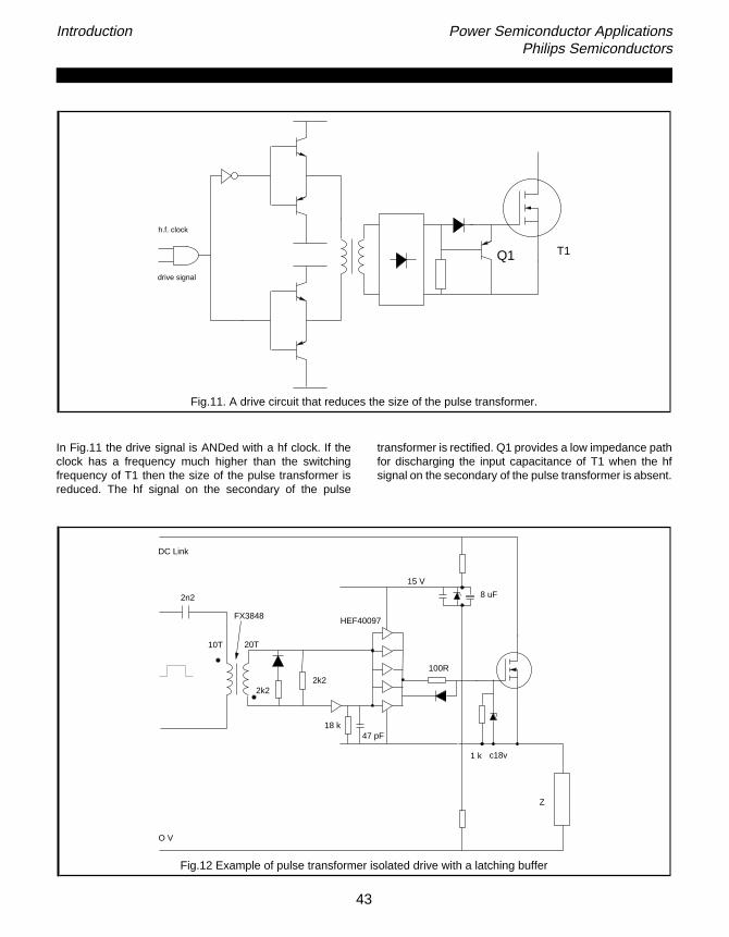
Introduction Power Semiconductor ApplicationsPhilips Semiconductors
Fig.11. A drive circuit that reduces the size of the pulse transformer.
T1Q1
h.f. clock
drive signal
In Fig.11 the drive signal is ANDed with a hf clock. If theclock has a frequency much higher than the switchingfrequency of T1 then the size of the pulse transformer isreduced. The hf signal on the secondary of the pulse
transformer is rectified. Q1 provides a low impedance pathfor discharging the input capacitance of T1 when the hfsignal on the secondary of the pulse transformer is absent.
Fig.12 Example of pulse transformer isolated drive with a latching buffer
15 V
Z
HEF40097
2k22k2
10T 20T
47 pF18 k
1 k c18v
DC Link
O V
100R
FX3848
8 uF2n2
43
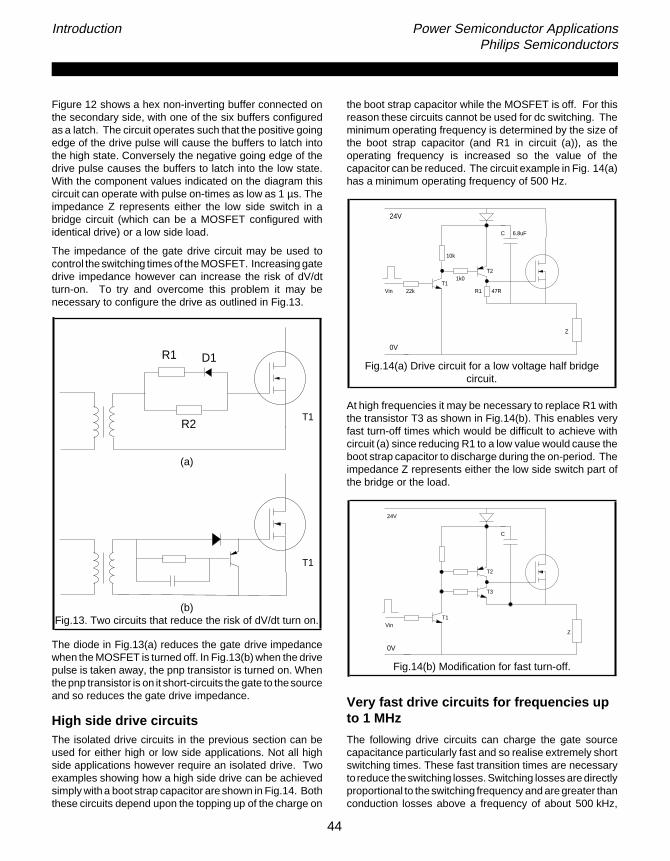
Introduction Power Semiconductor ApplicationsPhilips Semiconductors
Figure 12 shows a hex non-inverting buffer connected onthe secondary side, with one of the six buffers configuredas a latch. The circuit operates such that the positive goingedge of the drive pulse will cause the buffers to latch intothe high state. Conversely the negative going edge of thedrive pulse causes the buffers to latch into the low state.With the component values indicated on the diagram thiscircuit can operate with pulse on-times as low as 1 µs. Theimpedance Z represents either the low side switch in abridge circuit (which can be a MOSFET configured withidentical drive) or a low side load.
The impedance of the gate drive circuit may be used tocontrol the switching times of the MOSFET. Increasing gatedrive impedance however can increase the risk of dV/dtturn-on. To try and overcome this problem it may benecessary to configure the drive as outlined in Fig.13.
(a)
(b)Fig.13. Two circuits that reduce the risk of dV/dt turn on.
The diode in Fig.13(a) reduces the gate drive impedancewhen the MOSFET is turned off. In Fig.13(b) when the drivepulse is taken away, the pnp transistor is turned on. Whenthe pnp transistor is on it short-circuits the gate to the sourceand so reduces the gate drive impedance.
High side drive circuitsThe isolated drive circuits in the previous section can beused for either high or low side applications. Not all highside applications however require an isolated drive. Twoexamples showing how a high side drive can be achievedsimply with a boot strap capacitor are shown in Fig.14. Boththese circuits depend upon the topping up of the charge on
the boot strap capacitor while the MOSFET is off. For thisreason these circuits cannot be used for dc switching. Theminimum operating frequency is determined by the size ofthe boot strap capacitor (and R1 in circuit (a)), as theoperating frequency is increased so the value of thecapacitor can be reduced. The circuit example in Fig. 14(a)has a minimum operating frequency of 500 Hz.
Fig.14(a) Drive circuit for a low voltage half bridgecircuit.
At high frequencies it may be necessary to replace R1 withthe transistor T3 as shown in Fig.14(b). This enables veryfast turn-off times which would be difficult to achieve withcircuit (a) since reducing R1 to a low value would cause theboot strap capacitor to discharge during the on-period. Theimpedance Z represents either the low side switch part ofthe bridge or the load.
Fig.14(b) Modification for fast turn-off.
Very fast drive circuits for frequencies upto 1 MHz
The following drive circuits can charge the gate sourcecapacitance particularly fast and so realise extremely shortswitching times. These fast transition times are necessaryto reduce the switching losses. Switching losses are directlyproportional to the switching frequency and are greater thanconduction losses above a frequency of about 500 kHz,
VinT1
T2
C 6.8uF
R1 47R
10k
22k
1k0
Z
24V
0V
T1
D1R1
R2
T1
24V
VinT1
T2
C
T3
Z
0V
44

Introduction Power Semiconductor ApplicationsPhilips Semiconductors
although this crossover frequency is dependent on circuitconfiguration. Thus for operation above 500 kHz it isimportant to have fast transition times.
At frequencies below 500 kHz the circuit in Fig.15 is oftenused. Above 500 kHz the use of the DS0026 instead of the4049 is recommended. The DS0026 has a high currentsinking and sourcing capability of 2.5 A. It is a NationalSemiconductor device and is capable of charging acapacitance of 100 pF in as short a time as 25 ns.
Fig.15 A MOSFET drive circuit using a hex CMOSbuffered inverter IC
In Fig.16 the value of capacitor C1 is made approximatelyequal to the input capacitance of the driven MOSFET. Thusthe RC time constant for the charging circuit isapproximately halved. The disadvantage of thisarrangement is that a drive voltage of 30V instead of 15Vis needed because of the potential divider action of C1 andthe input capacitance of the driven MOSFET. A small valueof C1 would be ideal for a fast turn on time and a large valueof C1 would produce a fast turn off. The circuit in Fig.17replaces C1 by two capacitors and enables fast turn on andfast turn off.
Fig.16 A simple drive circuit with reduced effectiveinput capacitance
For the circuit in Fig.17 when MOSFET T1 is turned on thedriven MOSFET T3 is driven initially by a voltage VDD
feeding three capacitors in series, namely C1, C2 and theinput capacitance of T3. Since the capacitors are in seriestheir equivalent capacitance will be low and so the RC timeconstant of the charging circuit will be low. C1 is made lowto make the turn on time very fast.
Fig.17 A drive circuit with reduced effective inputcapacitance and prolonged reverse bias at turn off.
The voltage across C2 will then settle down to(VDD - VZD1) R2/(R1 + R2). Therefore the inclusion ofresistors R1 and R2 means that C2 can be made largerthan C1 and still have a large voltage across it before theturn off of T3. Thus C2 can sustain a reverse voltage acrossthe gate source of T3 for the whole of the turn off time. Theinitial discharging current will be given by Equation 3,
Making VDD large will make turn on and turn off times verysmall.
Fast switching speeds can be achieved with the push pullcircuit of Fig.19. A further improvement can be made byreplacing the bipolar devices by MOSFETs as shown inFig.20. The positions of the P and N channel MOSFETsmay be interchanged and connected in the alternativearrangement of Fig.21. However it is likely that oneMOSFET will turn on faster than the other turns off and sothe circuit in Fig.21 may cause a current spike during theswitching interval. The peak to average current rating ofMOSFETs is excellent so this current spike is not usuallya problem. In the circuit of Fig.20 the input capacitance ofthe driven MOSFET is charged up to VDD - VT, where VT isthe threshold voltage, at which point the MOSFET T1 turnsoff. Therefore when T2 turns on there is no current spike.
Vdd
T1
T2
T3
ZD1
C2R1 C1
ZD2
R2
4049
0 V
15 V
I =VZD1 +
R2.(VDD − VZD1)
(R1 + R2)
RSTRAY+ RDS(ON)T2
3
30 V
0 V
C1 = 2 nF
45

Introduction Power Semiconductor ApplicationsPhilips Semiconductors
Fig.18 A comparison of the switching times forMOSFETs driven from a constant current source and a
constant voltage source.
Fig.19 A push-pull drive circuit using bipolar transistors
There may well be some advantages in charging the inputcapacitance of the MOSFET from a constant current sourcerather than a constant voltage source. For a given drainsource voltage a fixed amount of charge has to betransferred to the input capacitance of a MOSFET to turnit on. As illustrated in Fig.18 this charge can be transferredmore quickly with a constant current of magnitude equal tothe peak current from a constant voltage source.
A few other points are worthy of note when discussing veryfast drive circuits.
(1) SMPS working in the 1 - 15 MHz range sometimes useresonant drive circuits. These SMPS are typically QRC(Quasi Resonant Circuits). The resonant drive circuits donot achieve faster switching by the fact that they areresonant. But by being resonant, they recoup some of thedrive energy and reduce the gate drive power. There aretwo main types of QRC - zero voltage and zero currentswitching circuits. In one of these types, fall times are notcritical and in the other, rise times are not critical. On the
critical switching edge, a normal, fast switching edge isprovided by using a circuit similar to those given above. Forthe non-critical edge there is a resonant transfer of energy.Thus drive losses of QG.VGS.f become 0.5.QG.VGS.f.
Fig.20 A push-pull drive circuit using MOSFETs in thecommon drain connection.
Fig.21 A push-pull drive circuit using MOSFETs in thecommon source connection
(2) It is usual toprovide overdrive of the gatesource voltage.This means charging the input capacitance to a voltagewhich is more than sufficient to turn the MOSFET fully on.This has advantages in achieving lower on-resistance andincreasing noise immunity. The gate power requirementsare however increased when overdrive is applied. It maywell be a good idea therefore to drive the gate with only12 V say instead of 15 V.
(3) It is recommended that a zener diode be connectedacross the gate source terminals of a MOSFET to protectagainst over voltage. This zener can have a capacitancewhich is not insignificant compared to the input capacitanceof small MOSFETs. The zener can thus affect switchingtimes.
Constant
Current
Constant
Voltage
A1
A2
A1 = A2T1
T2
time
time
I
I
Vdd
T1
T2
Vdd
T1
T2
46

Introduction Power Semiconductor ApplicationsPhilips Semiconductors
Parallel operation
Power MOSFETs lend themselves readily to operation inparallel since their positive temperature coefficient ofresistance opposes thermal runaway. Since MOSFETshave low gate drive power requirements it is not normallynecessary to increase the rating of drive circuit componentsif more MOSFETs are connected in parallel. It is howeverrecommended that differential resistors are used in thedrive circuits as shown in Fig.22.
Fig.22. A drive circuit suitable for successful parallellingof Philips MOSFETs incorporating differential resistors.
These differential resistors (RD) damp down possibleoscillations between reactive components in the device andin connections around the MOSFETs, with the MOSFETsthemselves, which have a high gain even up to 200 MHz.
Protection against gate-sourceovervoltagesIt is recommended that zener diodes are connected acrossthe gate-source terminals of the MOSFET to protect againstvoltage spikes. One zener diode or two back-to-back zenerdiodes are necessary dependent on whether thegate-source is unipolar or bipolar, as shown in Fig.23.
The zener diodes should be connected close to theterminals of the MOSFET to reduce the inductance of theconnecting leads. If the inductance of the connecting leadsis too large it can support sufficient voltage to cause anovervoltage across the gate-source oxide.
In conclusion the low drive power requirement of PhilipsPowerMOS make provision of gate drive circuitry arelatively straightforward process as long as the fewguide-lines outlined in this note are heeded.
RdRd
Fig.23. Zener diodes used to suppress voltage spikes across the gate-source terminals of the MOSFET.
T1
4011
47


Introduction Power Semiconductor ApplicationsPhilips Semiconductors
1.2.4 Parallel Operation of Power MOSFETs
This section is intended as a guide to the successfulparallelling of Power MOSFETs in switching circuits.
Advantages of operating devices inparallel
Increased power handling capabilityIf power requirements exceed those of available devicesthen increased power levels can be achieved by parallellingdevices. The alternative means of meeting the powerrequirements would be to increase the area of die. Theprocessing of the larger die would have a lower yield andso the relative cost of the die would be increased. The largerdie may also require a more expensive package.
StandardisationParallelling devices can mean that only one package, saythe TO220 package, needs to be used. This can result inreduced production costs.
Increased operating frequencyPackages are commercially available which contain uptofive die connected in parallel. The switching capabilities ofthese packages are typically greater than 10 kVA. Theparasitic inductances of connections to the parallelled diesare different for each die. This means that the current ratingof the package has to be derated at high frequencies toallow for unequal current sharing. The voltage rating of themultiple die package has to be derated for higher switchingspeeds. This is because the relatively large inductances ofconnections within the package sustain appreciablevoltages during the switching intervals. This means that thevoltages at the drain connections to the dice will beappreciably greater than voltages at the terminals of thepackage. By parallelling discrete devices these problemscan be overcome.
Faster switching speeds are achieved using parallelleddevices than using a multiple die package. This is becauseswitching times are adversely affected by the impedanceof the gate drive circuit. When devices are parallelled theseimpedances are parallelled and so their effect is reduced.Hence faster switching times and so reduced switchinglosses can be achieved.
Faster switching speeds improve parallelling. Duringswitching intervals one MOSFET may carry more currentthan other MOSFETs in parallel with it. This is caused bydifferences in electrical parameters between the parallelledMOSFETs themselves or between their drive circuits. Theincreased power dissipation in the MOSFET which carriesmore current will be minimised if switching speeds are
increased. The inevitable inductance in the sourceconnection, caused by leads within the package, causes anegative feedback effect during switching. If the rate of riseof current in one parallelled MOSFET is greater than in theothers then the voltage drop across inductances in its drainand source terminals will be greater. This will oppose thebuild up of current in this MOSFET and so have a balancingeffect. This balancing effect will be greater if switchingspeeds are faster. This negative feedback effect reducesthe deleterious effect of unequal impedances of drive circuitconnections to parallelled MOSFETs. The faster theswitching speeds then the greater will be the balancingeffect of the negative feedback. Parallelling devicesenables higher operating frequencies to be achieved thanusing multiple die packages. The faster switching speedspossible by parallelling at the device level promote bettercurrent sharing during switching intervals.
Increased power dissipation capability
If two devices, each rated for half the total required current,are parallelled then the sum of their individual powerdissipationcapabilities will be more than the possible powerdissipation in a single device rated for the total requiredcurrent. This is especially useful for circuits operating above100 kHz where switching losses predominate.
Fig.1. A typical graph of on resistance versustemperature for a Power MOSFET
-60 -20 20 60 100 140 180
2
1.9
1.8
1.7
1.6
1.5
1.4
1.3
1.2
1.1
1
0.9
0.8
0.7
0.6
0.5
0.4
0.3
0.2
0.1
0
Nor
mal
ised
Res
ista
nce
Junction Temperature ( C)
49

Introduction Power Semiconductor ApplicationsPhilips Semiconductors
Advantages of power MOSFETs forparallel operation
Reduced likelihood of thermal runawayIf one of the parallelled devices carries more current thenthe power dissipation in this device will be greater and itsjunction temperature will increase. The temperaturecoefficient of RDS(ON) for Power MOSFETs is positive asshown in Fig.1. Therefore there will be a rise in RDS(ON) forthe device carrying more current. This mechanism willoppose thermal runaway in parallelled devices and also inparallelled cells in the device.
Low Drive Power RequirementsThe low drive power requirements of power MOSFETsmean that many devices can be driven from the same gatedrive that would be used for one MOSFET.
Very good tolerance of dynamicunbalanceThe peak to average current carrying capability of powerMOSFETs is very good. A device rated at 8A continuousdrain current can typically withstand a peak current of about30A. Therefore, for the case of three 8A devices in parallel,if one of the devices switches on slightly before the othersno damage will result since it will be able to carry the fullload current for a short time.
Design points
DeratingSince there is a spread in on-resistance between devicesfrom different batches it is necessary to derate thecontinuous current rating of parallelled devices by about20%.
LayoutThere are two aspects to successful parallelling which arestatic and dynamic balance. Static balance refers to equalsharing of current between parallelled devices when theyhave been turned on. Dynamic balance means equalsharing of current between parallelled transistors duringswitching intervals.
Unsymmetrical layout of the circuit causes static imbalance.If the connections between individual MOSFETs and therest of the power circuit have different impedances thenthere will be static imbalance. The connections need to bekept as short as possible to keep their inductance as smallas possible. Symmetrical layout is particularly important inresonant circuits where MOSFETs carry a sinusoidalcurrent e.g. in a voltage fed inverter feeding a seriesresonant circuit. In a current fed inverter, where switchingin the inversion stage causes a rectangular wave of current
to be passed through a parallel resonant tank circuit, thevoltage sustained by MOSFETs when they are off will behalf sinusoid. A component of the current carried byMOSFETs will be a charging current for snubber capacitorswhich will be sinusoidal so again symmetrical layout will beimportant.
Fig.2. The waveforms of current through two parallelledBUK453-50A MOSFETs with symmetrical layout.
Fig.3. The waveforms of current through two parallelledBUK453-50A MOSFETS with 50 nH connected in the
source connection on one MOSFET.
Unsymmetrical layout of the gate drive circuitry causesdynamic imbalance. Connections between the gate drivecircuitry and the MOSFETs need to be kept short andtwisted together to reduce their inductance. Further to this
-500 -300 -100 100 300 500
50
40
30
20
10
0
-10
time (ns)
Cur
rent
(A
)
-500 -300 -100 100 300 500
50
40
30
20
10
0
-10
time (ns)
Cur
rent
(A
)
50

Introduction Power Semiconductor ApplicationsPhilips Semiconductors
the connections between the gate drive circuit andparallelled MOSFETs need to be approximately the samelength.
Figures 2 and 3 illustrate the effect of unsymmetrical layouton the current sharing of two parallelled MOSFETs. Thepresence of 50 nH in the source connection of one of thetwo parallelled BUK453-50A MOSFETs causes noticeableimbalance. A square shaped loop of 1 mm diameter wireand side dimension only 25 mm is sufficient to produce aninductance of 50 nH.
Symmetrical layout becomes more important if moreMOSFETs are parallelled, e.g. if a MOSFET with an RDS(ON)
of 0.7 Ohm was connected in parallel with a MOSFET withan RDS(ON) of 1 Ohm then the MOSFET with the lower RDS(ON)
would carry 18% more current that if both MOSFETs hadan RDS(ON) of 1 ohm. If the MOSFET with an RDS(ON) of 0.7ohm was connected in parallel with a hundred MOSFETswith RDS(ON) of 1 ohm it would carry 42% more current thanif all the MOSFETs had an RDS(ON) 1 Ohm.
Good Thermal Coupling
There should be good thermal coupling between parallelledMOSFETs. This is achieved by mounting parallelledMOSFETs on the same heatsink or on separate heatsinkswhich are in good thermal contact with each other.
If poor thermal coupling existed between parallelledMOSFETs and the positive temperature coefficient ofresistance was relied on to promote static balance, then thetotal current carried by the MOSFETs would be less thanwith good thermal coupling. Some MOSFETs would alsohave relatively high junction temperatures and so theirreliability would be reduced. The temperature coefficient ofMOSFETs is not large enough to make poor thermalcoupling tolerable.
The Suppression of Parasitic Oscillations
Parasitic oscillations can occur. MOSFETs have transitionfrequencies typically in excess of 200 MHz and parasiticreactances are present both in the MOSFET package andcircuit connections, so the necessary feedback conditionsfor parasitic oscillations exist. These oscillations typicallyoccur at frequencies above 100 MHz so a high bandwidthoscilloscope is necessary to investigate them. Thelikelihood of these parasitic oscillations occurring is verymuch reduced if small differential resistors are connectedin the leads to each parallelled MOSFET. A common gatedrive resistor of between 10 and 100 Ohms with differentialresistors of about 10 Ohm are recommended as shown inFig.4.
Fig.4. Differential gate drive resistors
The suppression of parasitic oscillations betweenparallelled MOSFETs can also be aided by passing theconnections from the gate drive circuit through ferritebeads. The effect of these beads below 1 MHz is negligible.The ferrite beads however damp the parasitic oscillationswhich occur at frequencies typically above 100 MHz. Anexample of parasitic oscillations is shown in Fig.5.
Fig.5. Parasitic oscillations on the voltage waveforms ofa MOSFET
If separate drive circuits with closely decoupled powersupplies are used for each parallelled device then parasiticoscillations will be prevented. This condition could besatisfied by driving each parallelled MOSFET from 3 buffersin a CMOS Hex buffer ic.
To take this one stage further, separate push pull transistordrivers could be used for each MOSFET. (A separate baseresistor is needed for each push-pull driver to avoid aMOSFET with a low threshold voltage clamping the drivevoltage to all the push pull drivers). This arrangement alsohas the advantage that the drive circuits can be positionedvery close to the terminals of each MOSFET. Theimpedance of connections from the drive circuits to theMOSFETs will be minimised and so there will be a reduced
10 Ohm10 Ohm
50 Ohm
0
5
10
15
0
10
20
30
40
Vds
(V
)V
gs (
V)
0 400 800 1200 1600 2000time (ns)
51

Introduction Power Semiconductor ApplicationsPhilips Semiconductors
likelihood of spurious turn on. Spurious turn on can occurwhen there is a fast change in the drain to source voltage.Thechargingcurrent for the gate drain capacitance inherentin the MOSFET structure can cause a voltage drop acrossthe gate drive impedance large enough to turn the MOSFETon. The gate drive impedance needs to be kept as low aspossible to reduce the likelihood of spurious turn on.
Resonant power suppliesIf a resonant circuit is used then there will be reducedinterference and switching losses. The reducedinterference is achieved because sinusoidal waveforms arepresent in resonant circuits rather than rectangularwaveforms. Rectangular waveforms have large highfrequency harmonic components.
MOSFETs are able to switch at a zero crossing of eitherthe voltage or the current waveform and so switching lossesare ideally zero. For example, in the case of a current fedinverter feeding a parallel resonant load switching can takeplace at a zero crossing of voltage so switching losses arenegligible. In this case the sinusoidal drain source voltagesustained by MOSFETs reduces the likelihood of spuriousdv/dt turn on. This is because the peak charging current forthe internal gate to drain capacitance of the MOSFET isreduced.
The current fed approachSwitch mode power supplies using the current fed topologyhave a d.c. link which contains a choke to smooth thecurrent in the link. Thus a high impedance supply ispresented to the inversion stage. Switching in the inversionstage causes a rectangular wave of current to be passedthrough the load. The current fed approach has manyadvantages for switch mode power supplies. It causesreduced stress on devices caused by the slow reverserecovery time of the parasitic diode inherent in the structureof MOSFETs.
Thecurrent fed approach canalso reduce problems causedby dynamic imbalance. If more than three MOSFETs areparallelled then it is advantageous to use more than onechoke in the d.c. link rather than wind a single choke out ofthicker gauge wire. One of the connections to each choke
is connected to the output of the rectification stage. Theother connection of each choke is connected to a group ofthree MOSFETs. This means that if one MOSFET switcheson before the others it will carry a current less than its peakpulse value even when many MOSFETs are parallelled.
The parallel operation of MOSFETs in thelinear mode
The problems of parallelling MOSFETs which are beingused in the linear mode are listed below.
(a) The parallelled devices have different thresholdvoltages and transconductances. This leads to poorsharing.
(b) MOSFETs have a positive temperature coefficient ofgain at low values of gate to source voltage. This can leadto thermal runaway.
The imbalance caused by differences in threshold voltageand transconductance can be reduced by connectingresistors (RS) in the source connections. These resistorsare in the gate drive circuit and so provide negativefeedback. The negative feedback reduces the effect ofdifferent values of VT and gm. The effectivetransconductance gm of the MOSFET is given inEquation 1.
RS must be large compared to 1/gm to reduce the effects ofdifferences in gm. Values of 1/gm typically vary between 0.1and 1.0 Ohm. Therefore values of RS between 1 ohm and10 ohm are recommended.
Differential heating usually has a detrimental effect onsharing and so good thermal coupling is advisable.
Conclusions
Power MOSFETs can successfully be parallelled to realisehigher power handling capability if a few guidelines arefollowed.
gm =1
Rs + 1
gm
1
52
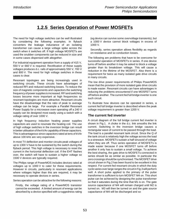
Introduction Power Semiconductor ApplicationsPhilips Semiconductors
1.2.5 Series Operation of Power MOSFETs
The need for high voltage switches can be well illustratedby considering the following examples. In flybackconverters the leakage inductance of an isolatingtransformer can cause a large voltage spike across theswitch when it switches off. If high voltage MOSFETs areused the snubber components can be reduced in size andin some cases dispensed with altogether.
For industrial equipment operation from a supply of 415 V,550 V or 660 V is required. Rectification of these supplyvoltages produces d.c. rails of approximately 550 V, 700 Vand 800 V. The need for high voltage switches in thesecases is clear.
Resonant topologies are being increasingly used inswitching circuits. These circuits have advantages ofreduced RFI and reduced switching losses. To reduce thesize of magnetic components and capacitors the switchingfrequency ofpower supplies is increased. RFIandswitchinglosses become more important at high frequencies soresonant topologies are more attractive. Resonant circuitshave the disadvantage that the ratio of peak to averagevoltage can be large. For example a Parallel ResonantPower Supply for a microwave oven operating off a 240 Vsupply can be designed most easily using a switch with avoltage rating of over 1000 V.
In high frequency induction heating power suppliescapacitors are used to resonate the heating coil. The useof high voltage switches in the inversion bridge can resultinbetter utilisation of the kVAr capabilityof thesecapacitors.This is advantageous since capacitors rated at tens of kVArabove 100 kHz are very expensive.
In most TV deflection and monitor circuits peak voltages ofup to 1300 V have to be sustained by the switch during theflyback period. This high voltage is necessary to reset thecurrent in the horizontal deflection coil. If the EHT flashesover, the switch will have to sustain a higher voltage so1500 V devices are typically required.
The Philips range of PowerMOS includes devices rated atvoltages up to 1000 V to cater for these requirements.However in circuits, particularly in resonant applicationswhere voltages higher than this are required, it may benecessary to operate devices in series.
Series operation can be attractive for the following reasons:
Firstly, the voltage rating of a PowerMOS transistorcannot be exceeded. A limited amount of energy can beabsorbed by a device specified with a ruggedness rating
(eg device can survive some overvoltage transients), buta 1000 V device cannot block voltages in excess of1000 V.
Secondly, series operation allows flexibility as regardson-resistance and so conduction losses.
The following are problems that have to be overcome forsuccessful operation of MOSFETs in series. If one deviceturns off before another it may be asked to block a voltagegreater than its breakdown voltage. This will cause areduction in the lifetime of the MOSFET. Also there is arequirement for twice as many isolated gate drive circuitsin many circuits.
The low drive power requirements of Philips PowerMOSmean that the provision of more isolated gate drive circuitsis made easier. Resonant circuits can have advantages inreducing the problems encountered if one MOSFET turnsoff before another. The current fed full bridge inverter is onesuch circuit.
To illustrate how devices can be operated in series, acurrent fed full bridge inverter is described where the peakvoltage requirement is greater than 1200 V.
The current fed inverterA circuit diagram of the full bridge current fed inverter isshown in Fig.1. A choke in the d.c. link smooths the linkcurrent. Switching in the inversion bridge causes arectangular wave of current to be passed through the load.The load is a parallel resonant tank circuit. Since the Q ofthe tank circuit is relatively high the voltage across the loadis a sinewave. MOSFETs sustain a half sinusoid of voltagewhen they are off. Thus series operation of MOSFETs ismade easier because if one MOSFET turns off beforeanother it only has to sustain a small voltage. To achievethe best sharing, the gate drive to MOSFETs connected inseries should be as similar as possible. In particular thezerocrossings should be synchronised.The MOSFETdrivecircuit shown in Fig.2 has been found to be excellent in thisrespect. For current fed resonant circuits in which the dutycyclevaries over large ranges the circuit in Fig.3 will performwell. A short pulse applied to the primary of the pulsetransformer is sufficient to turn MOSFET M4 on. This shortpulse can be achieved by designing the pulse transformerso that it saturates during the time that M1 is on. The gatesource capacitance of M4 will remain charged until M2 isturned on. M3 will then be turned on and the gate sourcecapacitance of M4 will be discharged and so
53
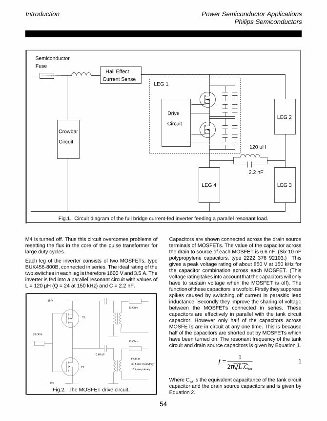
Introduction Power Semiconductor ApplicationsPhilips Semiconductors
Fig.1. Circuit diagram of the full bridge current-fed inverter feeding a parallel resonant load.
LEG 1
LEG 2
LEG 3LEG 4
Drive
Circuit
Crowbar
Circuit
Hall Effect
Current Sense
Semiconductor
Fuse
120 uH
2.2 nF
M4 is turned off. Thus this circuit overcomes problems ofresetting the flux in the core of the pulse transformer forlarge duty cycles.
Each leg of the inverter consists of two MOSFETs, typeBUK456-800B, connected in series. The ideal rating of thetwo switches in each leg is therefore 1600 V and 3.5 A. Theinverter is fed into a parallel resonant circuit with values ofL = 120 µH (Q = 24 at 150 kHz) and C = 2.2 nF.
Fig.2. The MOSFET drive circuit.
Capacitors are shown connected across the drain sourceterminals of MOSFETs. The value of the capacitor acrossthe drain to source of each MOSFET is 6.6 nF. (Six 10 nFpolypropylene capacitors, type 2222 376 92103.) Thisgives a peak voltage rating of about 850 V at 150 kHz forthe capacitor combination across each MOSFET. (Thisvoltage rating takes into account that the capacitors will onlyhave to sustain voltage when the MOSFET is off). Thefunction of these capacitors is twofold. Firstly they suppressspikes caused by switching off current in parasitic leadinductance. Secondly they improve the sharing of voltagebetween the MOSFETs connected in series. Thesecapacitors are effectively in parallel with the tank circuitcapacitor. However only half of the capacitors acrossMOSFETs are in circuit at any one time. This is becausehalf of the capacitors are shorted out by MOSFETs whichhave been turned on. The resonant frequency of the tankcircuit and drain source capacitors is given by Equation 1.
Where Ctot is the equivalent capacitance of the tank circuitcapacitor and the drain source capacitors and is given byEquation 2.
T1
T2
15 V
0 V
0.68 uF
FX3434
30 turns secondary
15 turns primary
33 Ohm
33 Ohm
33 Ohm
f =1
2π√L .Ctot
1
54
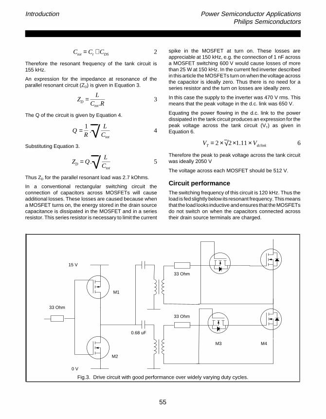
Introduction Power Semiconductor ApplicationsPhilips Semiconductors
Therefore the resonant frequency of the tank circuit is155 kHz.
An expression for the impedance at resonance of theparallel resonant circuit (ZD) is given in Equation 3.
The Q of the circuit is given by Equation 4.
Substituting Equation 3.
Thus ZD for the parallel resonant load was 2.7 kOhms.
In a conventional rectangular switching circuit theconnection of capacitors across MOSFETs will causeadditional losses. These losses are caused because whena MOSFET turns on, the energy stored in the drain sourcecapacitance is dissipated in the MOSFET and in a seriesresistor. This series resistor is necessary to limit the current
spike in the MOSFET at turn on. These losses areappreciable at 150 kHz, e.g. the connection of 1 nF acrossa MOSFET switching 600 V would cause losses of morethan 25 W at 150 kHz. In the current fed inverter describedin this article the MOSFETs turn on when the voltage acrossthe capacitor is ideally zero. Thus there is no need for aseries resistor and the turn on losses are ideally zero.
In this case the supply to the inverter was 470 V rms. Thismeans that the peak voltage in the d.c. link was 650 V.
Equating the power flowing in the d.c. link to the powerdissipated in the tank circuit produces an expression for thepeak voltage across the tank circuit (VT) as given inEquation 6.
Therefore the peak to peak voltage across the tank circuitwas ideally 2050 V
The voltage across each MOSFET should be 512 V.
Circuit performanceThe switching frequency of this circuit is 120 kHz. Thus theload is fed slightly below its resonant frequency. This meansthat the load looks inductive andensures that the MOSFETsdo not switch on when the capacitors connected acrosstheir drain source terminals are charged.
Ctot = Ct + CDS 2
ZD =L
Ctot.R3
Q =1R
.√ LCtot
4
VT = 2× √2×1.11× Vdclink 6
ZD = Q.√ LCtot
5
Fig.3. Drive circuit with good performance over widely varying duty cycles.
15 V
0 V
0.68 uF
33 Ohm
33 Ohm
33 Ohm
M1
M2
M3 M4
55

Introduction Power Semiconductor ApplicationsPhilips Semiconductors
The waveforms of the voltage across two MOSFETs inseries in a leg of the inversion bridge are shown in Fig.4. Itcan be seen that the sharing is excellent. The peak voltageacross each MOSFET is 600 V. This is higher than 512 Vbecause of ringing between parasitic lead inductance andthe drain source capacitance of MOSFETs when theyswitch off.
The MOSFETs carry two components of current. The firstcomponent is the d.c. link current. The second componentis a fraction of the circulating current of the tank circuit. Thesize of the second component is dependent on the relativesizes of the drain source capacitance connected acrossMOSFETs and the tank circuit capacitor.
In this circuit the peak value of charging current for drainsource capacitors, which is carried by the MOSFET, is 4 A.The on-resistance of the BUK456-800B is about 5 Ohmsat 80 ˚C. This explains the rise in VDS(ON) of about 20 V seenin Fig.4 just above the turn off of the MOSFETs.
The sharing of Philips PowerMOS in this configuration isso good that the value of drain source capacitance is notdetermined by its beneficial effect on sharing. Therefore,the value can be selected solely on the need to controlringing which in turn is dependent on power output andlayout. (The increased current level associated withincreased power output makes the ringing worse).
In any given configuration there is a maximum output powerthat single MOSFETs can handle and there will be a valueof drain source capacitance associated with it. This value
Fig.4. The drain-source voltage waveforms for twoMOSFETs connected in series in a leg of the inversion
bridge.
can be used as the ’capacitance per MOSFET’ in higherpower circuits where it becomes necessary to useMOSFETs connected in parallel. A value of between 5 and10 nF is probably sufficient given a sensible layout.
ConclusionsIt has been shown that MOSFETs can be connected inseries to realise a switch that is as high as 90% of the sumof the voltage sustaining capabilities of the individualtransistors.
0 13 26 39 52 65 78 91 104 117 1300
80
160
240
320
400
480
560
640
Dra
in-S
ourc
e V
olta
ge (
V)
time (us)
56

Introduction Power Semiconductor ApplicationsPhilips Semiconductors
1.2.6 Logic Level FETS
Standard Power MOSFETs require a gate-source voltageof 10 V to be fully ON. With Logic Level FETs (L2FETs)however, the same level of conduction is possible with agate-source voltage of only 5 V. They can, therefore, bedriven directly from 5 V TTL/CMOS ICs without the needfor the level shifting stages required for standardMOSFETs, see Fig.1. This makes them ideal for today’ssophisticated electrical systems, where microprocessorsare used to drive switching circuits.
Fig.1 Drive circuit for a standard MOSFET and anL2FET
This characteristic of L2FETs is achieved by reducing thegate oxide thickness from - 800 Angstroms to - 500Angstroms, which reduces the threshold voltage of thedevice from the standard 2.1-4.0 V to 1.0-2.0 V. Howeverthe result is a reduction in gate-source voltage ratings,from ±30 V for a standard MOSFET to ±15 V for the L2FET.The ±15 V rating is an improvement over the ’industrystandard’ of ±10 V, and permits Philips L2FETs to be usedin demanding applications such as automotive.
Although a 5 V gate-drive is ideal for L2FETs, they can beused in circuits with gate-drive voltages of up to 10 V. Using
a 10 V gate-drive results in a reduced RDS(ON) (see Fig.2)but the turn-off delay time is increased. This is due toexcessive charging of the L2FET’s input capacitance.
Fig.2 RDS(ON) as a function of VGS for a standardBUK453-100B MOSFET and a BUK553-100B L2FET. Tj
= 25 ˚C; VGS = 10 V
Capacitances, Transconductance andGate Charge
Figure3 shows the parasitic capacitances areas of a typicalPower MOSFET cell. Both the gate-source capacitanceCgs and the gate-drain capacitance Cgd increase due to thereduction in gate oxide thickness, although the increasein Cgd is only significant at low values of VDS, when thedepletion layer is narrow. Increases of the order of 25% ininput capacitance Ciss, output capacitance Coss and reversetransfer capacitance Crss result for the L2FET, comparedwith a similar standard type, at VDS = 0 V. However at thestandard measurement condition of VDS = 25 V thedifferences are virtually negligible.
Forward transconductance gfs is a function of the oxidethickness so the gfs of an L2FET is typically 40% - 50%higher than a standard MOSFET. This increase in gfs morethan offsets the increase in capacitance of an L2FET, sothe turn on charge requirement of the L2FET is lower thanthe standard type see Fig.4. For example, the standardBUK453-100B MOSFET requires about 17 nC to be fullyswitched on (at a gate voltage of 10 V) while theBUK553-100B L2FET only needs about 12 nC (at a gatesource voltage of 5 V).
input
TTL / CMOS
+10 V
VDD
StandardMOSFET
Standard MOSFET drive
input
TTL / CMOS
VDD
L FET drive2
L FET2
+5 V
57

Introduction Power Semiconductor ApplicationsPhilips Semiconductors
Fig.3 Parasitic capacitances of a typical PowerMOSFET cell
Fig.4 Turn-on gate charge curves of a standardBUK453-100B and a BUK553-100B L2FET. VDD = 20 V;
ID = 12 A
Switching speed.
Figure5 compares the turn-on performance of the standardBUK453-100B MOSFET and the BUK553-100B L2FET,under identical drive conditions of 5 V from a 50 Ωgenerator using identical loads. Thanks to its lower gatethreshold voltage VGST, the L2FET can be seen to turn onin a much shorter time from the low level drive.
Figure 6 shows the turn-off performance of the standardBUK453-100B MOSFET and the BUK553-100B L2FET,again with the same drive. This time the L2FET is slowerto switch. The turn-off times are determined mainly by thetime required for Cgd to discharge. The Cgd is higher for theL2FET at low VDS, and the lower value of VGST leads to alower discharging current. The net result is an increasein turn off time.
Fig.5 Comparison of (a) gate-source voltage and (b)drain-source voltage waveforms during turn-on of a
standard BUK453-100B MOSFET and a BUK553-100BL2FET. VGS is 5 V, ID is 3 A and VDD is 30 V.
Fast switching in many applications, for exampleautomotive circuits, is not important. In areas where it isimportant however the drive conditions should beexamined. For example, for a given drive power, a 10 Vdrive with a 50 Ω source impedance is equivalent to a 5 Vdrive with a source impedance of only 12 Ω. This results infaster switching for the L2FET compared with standardMOSFETs.
Ruggedness and reliabilityMOSFETs are frequently required to be able to withstandthe energy of an unclamped inductive load turn-off. Sincethis energy is dissipated in the bulk of the silicon, stressis avoided in the gate oxide. This means that theruggedness performance of L2FETs is comparable withthat of standard MOSFETs. The use of thinner gate oxidein no way compromises reliability. Good control of keyprocess parameters such as pinhole density, mobile ioncontent, interface state density ensures good oxide quality.The projected MTBF is 2070 years at 90˚C, at a 60%confidence level.
58

Introduction Power Semiconductor ApplicationsPhilips Semiconductors
Fig.6 Comparison of (a) gate-source voltage and (b)drain-source voltage waveforms during turn-off of a
standard BUK453-100B MOSFET and a BUK553-100BL2FET. VGS is 5 V, ID is 3 A and VDD is 30 V.
The VGS rating of an L2FET is about half that of a standardMOSFET,but thisdoes not affect the VDS rating. In principle,an L2FET version of any standard MOSFET is feasible.
Temperature stabilityIn general threshold voltage decreases with increasingtemperature. Although the threshold voltage of L2FETs islower than that of standard MOSFETs, so is theirtemperature coefficient of threshold voltage (about half infact), so their temperature stability compares favourablywith standard MOSFETs. Philips low voltage L2FETs(≤200v) in TO220 all feature Tjmax of 175˚C, rather thanthe industry standard of 150˚C.
ApplicationsThe Philips Components range of rugged Logic LevelMOSFETs enable cost effective drive circuit designwithout compromising ruggedness or reliability. Since theyenable power loads to be driven directly from ICs they maybe considered to be the first step towards intelligent powerswitching. Thanks to their good reliability and 175˚C Tjmax
temperature rating, they are displacing mechanical relaysin automotive body electrical functions and are beingdesigned in to such safety critical areas as ABS.
59


Introduction Power Semiconductor ApplicationsPhilips Semiconductors
1.2.7 Avalanche Ruggedness
Recent advances in power MOS processing technologynow enables power MOS transistors to dissipate energywhile operating in the avalanche mode. This feature resultsin transistors able to survive in-circuit momentaryovervoltage conditions, presenting circuit designers withincreased flexibility when choosing device voltage gradeagainst required safety margins.
This paper considers the avalanche characteristics of’rugged’ power MOSFETs and presents results frominvestigations into the physical constraints which ultimatelylimit avalanche energy dissipation in the VDMOS structure.Results suggest that the maximum sustainable energy is afunction of the applied power density waveform,independent of device voltage grade and chip size.
The ability of a rugged device to operate reliably in a circuitsubject to extreme interference is also demonstrated.
Introduction.Susceptibility to secondary breakdown is a phenomenonwhich limits the power handling capability of a bipolartransistor to below its full potential. For a power MOSFET,power handling capability is a simple function of thermalresistance and operating temperature since the device isnot vulnerable to a second breakdown mechanism. Theprevious statement holds true provided the device isoperated at or below its breakdown voltage rating (BVDSS)and not subject to overvoltage. Should the transistor beforced into avalanche by a voltage surge the structure ofthe device permits possible activation of a parasitic bipolartransistor which may then suffer the consequences ofsecond breakdown. In the past this mechanism was typicalof failure in circuits where the device became exposed toovervoltage. To reduce the risk of device failure duringmomentaryoverloads improvements have been introducedto the Power MOS design which enable it to dissipateenergy while operating in the avalanche condition. The termcommonly used to describe this ability is ’Ruggedness’,however before discussing in further detail the merits of arugged Power MOSFET it is worth considering the failuremechanism of non-rugged devices.
Failure mechanism of a non-rugged PowerMOS.A power MOS transistor is made up of many thousands ofcells, identical in structure. The cross section of a typicalcell is shown in Fig. 1. When in the off-state or operating insaturation, voltage is supported across the p-n junction asshown by the shaded region. If the device is subjected toover-voltage (greater than the avalanche value of the
device), the peak electric field, located at the p-n junction,rises to the critical value (approx. 200 kV / cm ) at whichavalanche multiplication commences.
Computer modelling has shown that the maximum electricfield occurs at the corners of the P diffusions. Theelectron-hole plasma generated by the avalanche processin these regions gives rise to a source of electrons, whichare swept across the drain, and a source of holes, whichflow through the P- and P regions towards the source metalcontact.
Fig. 1 Cross section of a typical Power MOS cell.
Clearly the P- region constitutes a resistance which will giverise to a potential drop beneath the n+. If this resistance istoo large the p-n junction may become forward biased forrelatively low avalanche currents.
Also if the manufacturing process does not yield a uniformcell structure across the device or if defects are present inthe silicon then multiplication may be a local event withinthe crystal. This would give rise to a high avalanche currentdensity flowing beneath the source n+ and cause arelatively large potential drop sufficient to forward bias thep-n junction and hence activate the parasitic npn bipolartransistor inherent in the MOSFET structure. Due to thepositive temperature coefficient associated with a forwardbiased p-n junction, current crowding will rapidly ensue withthe likely result of second breakdown and eventual devicedestruction.
N+ Substrate
N- Layer
P
P-P-
N+ N+
Source Contact Metal
Polysilicon Gate
Drain
SourceParasitic
Bipolar
Transistor
61

Introduction Power Semiconductor ApplicationsPhilips Semiconductors
In order that a power MOS transistor may survive transitoryexcursions into avalanche it is necessary to manufacture adevice with uniform cell structure, free from defectsthroughout the crystal and that within the cell the resistancebeneath the n+ should be kept to a minimum. In this way aforward biasing potential across the p-n junction is avoided.
Definition of ruggedness.The term ’Ruggedness’ when applied to a power MOStransistor, describes the ability of that device to dissipateenergy while operating in the avalanche condition. To testruggedness of a device it is usual to use the method ofunclamped inductive load turn-off using the circuit drawn inFig. 2.
Fig. 2 Unclamped inductive load test circuit forruggedness evaluation.
Fig. 3 Typical waveforms taken from the unclampedinductive load test circuit.
Circuit operation:-
A pulse is applied to the gate such that the transistor turnson and load current ramps up according to the inductorvalue, L and drain supply voltage, VDD. At the end of thegate pulse, channel current in the power MOS begins to fallwhile voltage on the drain terminal rises rapidly inaccordance with equation 1.
The voltage on the drain terminal is clamped by theavalanche voltage of the Power MOS for a duration equalto that necessary for dissipation of all energy stored in theinductor. Typical waveforms showing drain voltage andsource current for a device undergoing successful test areshown in Fig. 3.
The energy stored in the inductor is given by equation 2where ID is the peak load current at the point of turn-off ofthe transistor.
All this energy is dissipated by the Power MOS while thedevice is in avalanche.
Provided the supply rail is kept below 50 % of the avalanchevoltage, equation 2 approximates closely to the total energydissipation by the device during turn-off. However a moreexact expression which takes account of additional energydelivered from the power supply is given by equation 3.
Clearly the energy dissipated is a function of both theinductor value and the load current ID, the latter being setby the duration of the gate pulse. The 50 Ohm resistorbetween gate and source is necessary to ensure a fastturn-off such that the device is forced into avalanche.
The performance of a non-rugged device in response to theavalanche test is shown in Fig. 4. The drain voltage risesto the avalanche value followed by an immediate collapseto approximately 30 V. This voltage is typical of thesustaining voltage during Second Breakdown of a bipolartransistor, [1]. The subsequent collapse to zero volts after12 µS signifies failure of the device. The transistor shownhere was only able to dissipate a few micro joules at a verylow current if a failure of this type was to be avoided.
dvdt
= Ld2I
dt2(1)
L
T.U.T.
VDD
RGSR 01
VDS
-ID/100
+
-
shunt
VGS
0 WDSS= 0.5LID2 (2)
WDSS=BVDSS
BVDSS− VDD
0.5LID2 (3)
62

Introduction Power Semiconductor ApplicationsPhilips Semiconductors
Fig. 4 Failure waveforms of a non rugged Power MOStransistor.
Fig. 5 Power and energy waveforms prior to failure for atypical BUK627-500B
Characteristics of a rugged Power MOS.
i) The energy limitation of a rugged deviceThe power waveform for a BUK627-500B (500 V, 0.8 Ohm)tested at a peak current of 15 A is presented in Fig. 5.
The area within the triangle represents the maximumenergy that this particular device type may sustain withoutfailure at the above current. Figure 6 shows the junctiontemperature variation in response to the power pulse,calculated from the convolution integral as shown inequation 4.
where transient thermal impedance.
Fig. 6 Junction temperature during the power pulse forthe avalanche ruggedness test on a Philips
BUK627-500B.
Equation 4 predicts that the junction temperature will passthrough a maximum of 325 ˚C during the test. Thecalculation of Zth(t) assumes that the power dissipation isuniform across the active area of the device. When thedevice operates in the avalanche mode the power will bedissipated more locally in the region of the p-n junctionwhere the multiplication takes place. Consequently a localtemperature above that predicted by equation 4 is likely tobe present within the device.
Work on bipolar transistors [2] has shown that at atemperature of the order of 400 ˚C, the voltage supportingp-n region becomes effectively intrinsic as a result ofthermal multiplication, resulting in a rapid collapse in theterminal voltage. It is probable that a similar mechanism isresponsible for failure of the Power MOS with a localtemperature approaching 400 ˚C resulting in a device shortcircuit. A subsequent rapid rise in internal temperature willresult in eventual device destruction.
Clearly the rise in Tj is a function of the applied powerwaveform which is in turn related to circuit current,avalanche voltage of the device and duration of the energypulse.Thus the energy required to bringabout device failurewill vary as a function of each of these parameters. Theruggedness of Power MOSFETS of varying crystal size andvoltage specification together with dependence on circuitcurrent is considered below.
ii) Sustainable avalanche energy as afunction of current.The typical avalanche energy required to cause devicefailure is plotted as a function of peak current in Fig. 7 fora BUK553-60A (60 V, 0.085 Ohm Logic Level device). Thisresult was obtained through destructive device testingusing the circuit of Fig. 2 and a variety of inductor values.
Tj(t) = ⌠⌡τ = 0
τ = t
P(t − τ)Zth(τ)dτ (4)
Zth(τ) =
63
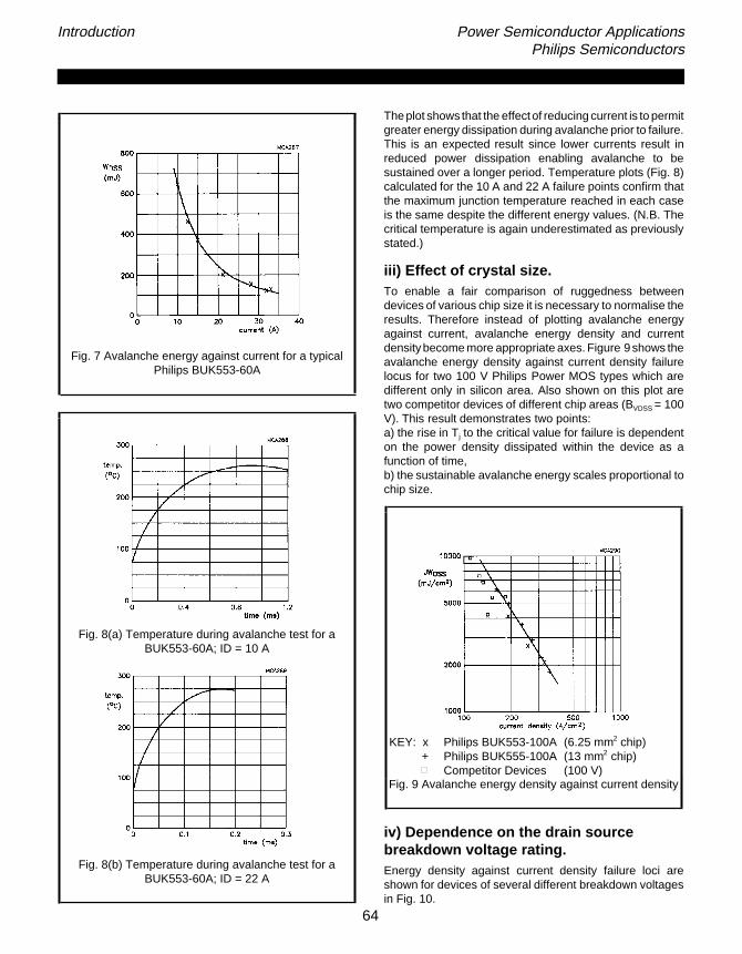
Introduction Power Semiconductor ApplicationsPhilips Semiconductors
Fig. 7 Avalanche energy against current for a typicalPhilips BUK553-60A
Fig. 8(a) Temperature during avalanche test for aBUK553-60A; ID = 10 A
Fig. 8(b) Temperature during avalanche test for aBUK553-60A; ID = 22 A
Theplot shows that the effectof reducing current is to permitgreater energy dissipation during avalanche prior to failure.This is an expected result since lower currents result inreduced power dissipation enabling avalanche to besustained over a longer period. Temperature plots (Fig. 8)calculated for the 10 A and 22 A failure points confirm thatthe maximum junction temperature reached in each caseis the same despite the different energy values. (N.B. Thecritical temperature is again underestimated as previouslystated.)
iii) Effect of crystal size.To enable a fair comparison of ruggedness betweendevices of various chip size it is necessary to normalise theresults. Therefore instead of plotting avalanche energyagainst current, avalanche energy density and currentdensitybecome more appropriate axes. Figure 9 shows theavalanche energy density against current density failurelocus for two 100 V Philips Power MOS types which aredifferent only in silicon area. Also shown on this plot aretwo competitor devices of different chip areas (BVDSS = 100V). This result demonstrates two points:a) the rise in Tj to the critical value for failure is dependenton the power density dissipated within the device as afunction of time,b) the sustainable avalanche energy scales proportional tochip size.
KEY: x Philips BUK553-100A (6.25 mm2 chip)+ Philips BUK555-100A (13 mm2 chip)
Competitor Devices (100 V)Fig. 9 Avalanche energy density against current density
iv) Dependence on the drain sourcebreakdown voltage rating.Energy density against current density failure loci areshown for devices of several different breakdown voltagesin Fig. 10.
64

Introduction Power Semiconductor ApplicationsPhilips Semiconductors
KEY: x Philips BUK553-60A+ Philips BUK555-100A
Philips BUK627-500BFig. 10 Avalanche energy density against current
density
Presented in this form it is difficult to assess the relativeruggedness of each device since the current density isreduced for increasing voltage. If instead of peak currentdensity, peak power density is used for the x-axis thencomparison is made very simple. The data of Fig. 10 hasbeen replotted in Fig. 11 in the above manner. Representedin this fashion the ruggedness of each chip appears verysimilar highlighting that the maximum energy dissipation ofa device while in avalanche is dependent only on the powerdensity function.
KEY: x Philips BUK553-60A+ Philips BUK555-100A
Philips BUK627-500BFig. 11 Avalanche energy density against peak power
density
Ruggedness ratings.
It should be stressed that the avalanche energiespresentedin the previous section result in a rise of the junctiontemperature far in excessof the device rating and in practiceenergies should be kept within the specification.Ruggedness is specified in data for each device in termsof an unclamped inductive load test maximum condition;recommended energy dissipation at a particular current(usually the rated current of the device).
DEVICE RDSON VDS ID WDSS
TYPE (Ω) (V) (A) (mJ)
BUK552-60A 0.15 60 14 30
BUK552-100A 0.28 100 10 30
BUK553-60A 0.085 60 20 45
BUK553-100A 0.18 100 13 70
Table 1 Ruggedness Ratings
The ruggedness rating is chosen to protect against a risein Tj above the maximum rating. Examples of ruggednessratings for asmall selection ofdevices are shown in Table 1.
Fig. 12 Normalised temperature derating curve
This data is applicable for Tj = 25 C. For higher operatingtemperatures the permissible rise in junction temperatureduring the energy test is reduced. Consequentlyruggedness needs to be derated with increasing operatingtemperature. A normalised derating curve for devices withTj max 175 ˚C is presented in Fig. 12.
20 40 60 80 100 120 140 160 180Tmb / C
120
110
100
90
80
70
60
50
40
30
20
10
0
WDSS%
65

Introduction Power Semiconductor ApplicationsPhilips Semiconductors
Fig. 13(a) Test circuit
Fig. 13(b) Output from transient generator.
Performance of a rugged Power MOSdevice.The ability of a rugged Power MOS transistor to survivemomentary power surges results in excellent devicereliability. The response of a BUK553-60A to interferencespikes while switching a load is presented below. The test
circuit is shown in Fig. 13(a) together with the profile of theinterference spike in Fig. 13(b).
The interference generator produces pulses asynchronousto the switching frequency of the Power MOS. Figure 14shows the drain voltage and load current response at fourinstances in the switching cycle. Devices were subjectedto 5000 interference spikes at a frequency of 5 Hz. Nodegradation in device performance was recorded.
Conclusions.The ability of power MOS devices to dissipate energy in theavalanche mode has been made possible by processoptimisation to remove the possibility of turn-on of theparasitic bipolar structure. The failure mechanism of arugged device is one of excessive junction temperatureinitiating a collapse in the terminal voltage as the junctionarea becomes intrinsic. The rise in junction temperature isdictated by the power density dissipation which is a functionof crystal size, breakdown voltage and circuit current.
Ruggedness ratings for Philips PowerMOS are chosen toensure that the specified maximum junction temperature ofthe device is not exceeded.
References.1. DUNN and NUTTALL, An investigation of the voltage
sustained by epitaxial bipolar transistors in currentmode second breakdown. Int.J.Electronics, 1978,vol.45, no.4, 353-372
2. DOW and NUTTALL, A study of the current distributionestablished in npn epitaxial transistors during currentmode second breakdown. Int.J.Electronics, 1981,vol.50, no.2, 93-108
T.U.T.
50 R
VDS
7.5 V
014 V DC
SOURCE
TRANSIENT
GENERATOR
14 V38 WLAMP
20 R
100 Hz - 1 kHz
50 % DUTY CYCLE
SQUARE WAVE
t1 = point of turn-on of PowerMOSt2 = point of turn-off of PowerMOS
Fig. 14 VDS and ID waveforms for the circuit in Fig. 13(a)
66
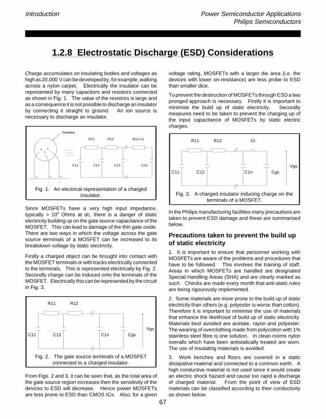
Introduction Power Semiconductor ApplicationsPhilips Semiconductors
1.2.8 Electrostatic Discharge (ESD) Considerations
Charge accumulates on insulating bodies and voltages ashighas 20,000 Vcan be developedby, forexample, walkingacross a nylon carpet. Electrically the insulator can berepresented by many capacitors and resistors connectedas shown in Fig. 1. The value of the resistors is large andas a consequence it is not possible to dischargean insulatorby connecting it straight to ground. An ion source isnecessary to discharge an insulator.
Fig. 1. An electrical representation of a chargedinsulator.
Since MOSFETs have a very high input impedance,typically > 109 Ohms at dc, there is a danger of staticelectricity building up on the gate source capacitance of theMOSFET. This can lead to damage of the thin gate oxide.There are two ways in which the voltage across the gatesource terminals of a MOSFET can be increased to itsbreakdown voltage by static electricity.
Firstly a charged object can be brought into contact withthe MOSFET terminals or with tracks electrically connectedto the terminals. This is represented electrically by Fig. 2.Secondly charge can be induced onto the terminals of theMOSFET. Electrically this can be represented by the circuitin Fig. 3.
Fig. 2. The gate source terminals of a MOSFETconnected to a charged insulator.
From Figs. 2 and 3, it can be seen that, as the total area ofthe gate source region increases then the sensitivity of thedevices to ESD will decrease. Hence power MOSFETsare less prone to ESD than CMOS ICs. Also, for a given
voltage rating, MOSFETs with a larger die area (i.e. thedevices with lower on-resistance) are less probe to ESDthan smaller dice.
To prevent the destruction of MOSFETs through ESD a twopronged approach is necessary. Firstly it is important tominimise the build up of static electricity. Secondlymeasures need to be taken to prevent the charging up ofthe input capacitance of MOSFETs by static electriccharges.
Fig. 3. A charged insulator inducing charge on theterminals of a MOSFET.
In the Philips manufacturing facilities many precautions aretaken to prevent ESD damage and these are summarisedbelow.
Precautions taken to prevent the build upof static electricity1. It is important to ensure that personnel working withMOSFETs are aware of the problems and procedures thathave to be followed. This involves the training of staff.Areas in which MOSFETs are handled are designatedSpecial Handling Areas (SHA) and are clearly marked assuch. Checks are made every month that anti-static rulesare being rigourously implemented.
2. Some materials are more prone to the build up of staticelectricity than others (e.g. polyester is worse than cotton).Therefore it is important to minimise the use of materialsthat enhance the likelihood of build up of static electricity.Materials best avoided are acetate, rayon and polyester.The wearing of overclothing made from polycotton with 1%stainless steel fibre is one solution. In clean rooms nylonoveralls which have been antistatically treated are worn.The use of insulating materials is avoided.
3. Work benches and floors are covered in a staticdissipative material and connected to a common earth. Ahigh conductive material is not used since it would createan electric shock hazard and cause too rapid a dischargeof charged material. From the point of view of ESDmaterials can be classified according to their conductivityas shown below.
Insulator
++
+
- - -
C11 C12 C13 C1n
R11 R12 R(1n-1)
C11 C12
R11 R12
C1n CgsVgs
Ct
C11 C12
R11 R12
C1n CgsVgs
67

Introduction Power Semiconductor ApplicationsPhilips Semiconductors
insulator (>1014 ohm/square)
antistatic (109 - 1014 Ohm/square)
static dissipative (105 - 109 Ohm/square)
conductor (<105 Ohm/square).
4. Conducting straps are used to electrically connectpersonnel to the point of common earthing. This preventsthe build up of static charge on staff. The connection isstatic dissipative to prevent an electric shock hazard.
5. Air plays an important part in the build up of staticelectricity.
This is particularly troublesome in a dry atmosphere.
Many of the techniques mentioned above are referred to inBS5783.
Precautions taken to prevent damage toMOSFETs by electrostatic build up ofcharge1. When MOSFETs are being transported or stored they
should be in antistatic containers. These containers shouldbe totally enclosed to prevent charges being induced ontothe terminals of devices.
2. If MOSFETs have to be left out on the bench, e.g. duringa test sequence, they should be in sockets which have thegate and source pins electrically connected together.
The precautions that should be taken at the customers’premises are the sameas above. It should be rememberedthat whenever a MOSFET is touched by someone there isa danger of damage. The precautions should be taken inevery area in which MOSFETs are tested or handled. Inaddition where devices are soldered into circuits with asoldering iron an earthed bit should always be used.
The probability of device destruction caused by ESD is loweven if only the most rudimentary precautions are taken.However without such precautions and with large numbersof PowerMOS devices now being designed into equipmenta few failures would be inevitable. The adoption of theprecautions outlined will mean that ESD will no longer bea problem.
68
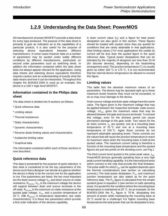
Introduction Power Semiconductor ApplicationsPhilips Semiconductors
1.2.9 Understanding the Data Sheet: PowerMOS
All manufacturers of power MOSFETs provide a data sheetfor every type produced. The purpose of the data sheet isprimarily to give an indication as to the capabilities of aparticular product. It is also useful for the purpose ofselecting device equivalents between differentmanufacturers. In some cases however data on a numberof parameters may be quoted under subtly differentconditions by different manufacturers, particularly onsecond order parameters such as switching times. Inaddition the information contained within the data sheetdoes not always appear relevant for the application. Usingdata sheets and selecting device equivalents thereforerequires caution and an understanding of exactly what thedata means and how it can be interpreted. Throughout thischapter the BUK553-100A is used as an example, thisdevice is a 100 V logic level MOSFET.
Information contained in the Philips datasheet
The data sheet is divided into 8 sections as follows:
* Quick reference data
* Limiting values
* Thermal resistances
* Static characteristics
* Dynamic characteristics
* Reverse diode limiting values and characteristics
* Avalanche limiting value
* Graphical data
The information contained within each of these sections isnow described.
Quick reference data
This data is presented for the purpose of quick selection. Itlists what is considered to be the key parameters of thedevice such that a designer can decide at a glance whetherthe device is likely to be the correct one for the applicationor not. Five parameters are listed, the two most importantare the drain-source voltage VDS and drain-source on-stateresistance, RDS(ON). VDS is the maximum voltage the devicewill support between drain and source terminals in theoff-state. RDS(ON) is the maximum on-state resistance at thequoted gate voltage, VGS, and a junction temperature of25 ˚C. (NB RDS(ON) is temperature dependent, see staticcharacteristics). It is these two parameters which providea first order indication of the devices capability.
A drain current value (ID) and a figure for total powerdissipation are also given in this section. These figuresshould be treated with caution since they are quoted forconditions that are rarely attainable in real applications.(See limiting values.) For most applications the usable dccurrent will be less than the quoted figure in the quickreference data. Typical power dissipations that can betolerated by the majority of designers are less than 20 W(for discrete devices), depending on the heatsinkingarrangement used. The junction temperature (TJ) is usuallygiven as either 150 ˚C or 175 ˚C. It is not recommendedthat the internal device temperature be allowed to exceedthis figure.
Limiting valuesThis table lists the absolute maximum values of sixparameters. The device may be operated right up to thesemaximum levels however they must not be exceeded, todo so may incur damage to the device.
Drain-source voltageand drain-gate voltage have the samevalue. The figure given is the maximum voltage that maybe applied between the respective terminals. Gate-sourcevoltage, ±VGS, gives the maximum value that may beallowed between the gate and source terminals. To exceedthis voltage, even for the shortest period can causepermanent damage to the gate oxide. Two values for thedc drain current, ID, are quoted, one at a mounting basetemperature of 25 ˚C and one at a mounting basetemperature of 100 ˚C. Again these currents do notrepresent attainable operating levels. These currents arethe values that will cause the junction temperature to reachits maximum value when the mounting base is held at thequoted value. The maximum current rating is therefore afunction of the mounting base temperature and the quotedfigures are just two points on the derating curve ,see Fig.1.
The third current level quoted is the pulse peak value, IDM.PowerMOS devices generally speaking have a very highpeak current handling capability. It is the internal bond wireswhich connect to the chip that provide the final limitation.The pulse width for which IDM can be applied depends uponthe thermal considerations (see section on calculatingcurrents.) The total power dissipation, Ptot, and maximumjunction temperature are also stated as for the quickreference data. The Ptot figure is calculated from the simplequotient given in equation 1 (see section on safe operatingarea). It is quoted for the conditionwhere the mounting basetemperature is maintained at 25 ˚C. As an example, for theBUK553-100A the Ptot figure is 75 W, dissipating thisamount of power while maintaining the mounting base at25 ˚C would be a challenge! For higher mounting basetemperatures the total power that can be dissipated is less.
69

Introduction Power Semiconductor ApplicationsPhilips Semiconductors
Fig.1 Normalised continuous drain current.ID% = 100 . ID/ID25 ˚C = f(Tmb); conditions: VGS ≥ 5 V
Obviously if the mounting base temperature was madeequal to the max permitted junction temperature, then nopower could be dissipated internally. A derating curve isgiven as part of the graphical data, an example is shown inFig.2 for a device with a limiting Tj of 175 ˚C.
Fig.2 Normalised power dissipation.PD% = 100 PD/PD 25 ˚C = f(Tmb)
Storage temperature limits are also quoted, usuallybetween -40 /-55 ˚C and +150 /+175 ˚C. Both the storagetemperature limits and the junction temperature limit arefigures at which extensive reliability work is performed byour Quality department. To exceed these figures will causea reduction in long-term reliability.
Thermal resistance.For non-isolated packages two thermal resistance valuesare given. The value from junction to mounting base (Rthj-mb)indicates how much the junction temperature will be raisedabove the temperature of the mounting base whendissipating a given power. Eg a BUK553-100A has a Rthj-mb
of 2 K/W, dissipating 10 W, the junction temperature will be20 ˚C above the temperature of its mounting base. Theother figure quoted is from junction to ambient. This is amuch larger figure and indicates how the junctiontemperature will rise if the device is NOT mounted on aheatsink but operated in free air. Eg for a BUK553-100A,Rthj-a = 60 K/W, dissipating 1 W while mounted in free airwill produce a junction temperature 60 ˚C above theambient air temperature.
For isolated packages, (F-packs) the mounting base (themetal plate upon which the silicon chip is mounted) is fullyencapsulated in plastic. Therefore it is not possible to givea thermal resistance figure junction to mounting base.Instead a figure is quoted from junction to heatsink, Rthj-hs,which assumes the use of heatsink compound. Care shouldbe taken when comparing thermal resistances of isolatedand non-isolated types. Consider the following example:
The non-isolated BUK553-100A has a Rthj-mb of 2 K/W. Theisolated BUK543-100A has a Rthj-hs of 5 K/W. These deviceshave identical crystals but mounted in different packages.At first glance the non-isolated type might be expected tooffer much higher power (and hence current) handlingcapability. However for the BUK553-100A the thermalresistance junction to heatsink has to be calculated, thisinvolves adding the extra thermal resistance betweenmounting base and heatsink. For most applications someisolation is used, such as a mica washer. The thermalresistance mounting base to heatsink is then of the order2 K/W. The total thermal resistance junction to heatsink istherefore
Rthj-hs (non isolated type) = Rthj-mb + Rthmb-hs = 4 K/W
It can be seen that the real performance difference betweenthe isolated and non isolated types will not be significant.
Static CharacteristicsThe parameters in this section characterise breakdownvoltage, threshold voltage, leakage currents andon-resistance.
A drain-source breakdown voltage is specified as greaterthan the limiting value of drain-source voltage. It can bemeasured on a curve tracer, with gate terminal shorted tothe source terminal, it is the voltage at which a drain currentof 250 µA is observed. Gate threshold voltage, VGS(TO),indicates the voltage required on the gate (with respect tothe source) to bring the device into its conducting state. Forlogic level devices this is usually between 1.0 and 2.0 Vand for standard devices between 2.1 and 4 V.
0 20 40 60 80 100 120 140 160 180Tmb / C
ID% Normalised Current Derating120
110
100
90
80
70
60
50
40
30
20
10
0
0 20 40 60 80 100 120 140 160 180Tmb / C
PD% Normalised Power Derating120
110
100
90
80
70
60
50
40
30
20
10
0
70

Introduction Power Semiconductor ApplicationsPhilips Semiconductors
Fig.3 Typical transfer characteristics.ID = f(VGS); conditions: VDS = 25 V; parameter Tj
Useful plots in the graphical data are the typical transfercharacteristics (Fig.3) showing drain current as a functionof VGS and the gate threshold voltage variation with junctiontemperature (Fig.4). An additional plot also provided is thesub-threshold conduction, showing how the drain currentvaries with gate-source voltage below the threshold level(Fig.5).
Off-state leakage currents are specified for both thedrain-source and gate-source under their respectivemaximum voltage conditions. Note, although gate-sourceleakage current is specified in nano-amps, values aretypically of the order of a few pico-amps.
Fig.4 Gate threshold voltage.VGS(TO) = f(Tj); conditions: ID = 1 mA; VDS = VGS
Fig.5 Sub-threshold drain current.ID = f(VGS); conditions: Tj = 25 ˚C; VDS = VGS
Fig.6 Typical output characteristics, Tj = 25 ˚C.ID = f(VDS); parameter VGS
The drain-source on-resistance is very important. It isspecifiedat a gate-source voltage of 5 V for logic level FETsand 10 V for a standard device. The on-resistance for astandard MOSFET cannot be reduced significantly byincreasing the gate source voltage above 10 V. Reducingthe gate voltage will however increase the on-resistance.For the logic level FET, the on-resistance is given for a gatevoltage of 5 V, a further reduction is possible however atgate voltages up to 10 V, this is demonstrated by the outputcharacteristics, Fig.6 and on-resistance characteristics,Fig.7 for a BUK553-100A. .
0 2 4 6 8
BUK543-100A
VGS / V
15
10
5
0
ID / A
Tj / C = 25 150
0 0.4 0.8 1.2 1.6 2 2.4VGS / V
ID / A1E-01
1E-02
1E-03
1E-04
1E-05
1E-06
SUB-THRESHOLD CONDUCTION
2 % typ 98 %
0 2 4 6 8 10
BUK553-100A
VDS / V
24
20
16
12
8
4
0 2
3
4
57
10ID / A
VGS / V =
-60 -20 20 60 100 140 180Tj / C
VGS(TO) / V
2
1
0
max.
typ.
min.
71
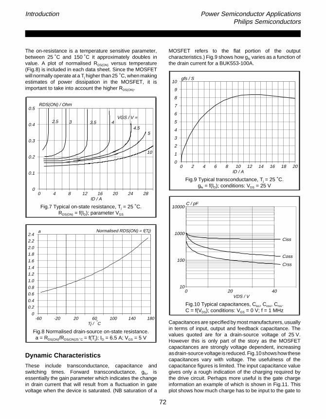
Introduction Power Semiconductor ApplicationsPhilips Semiconductors
The on-resistance is a temperature sensitive parameter,between 25 ˚C and 150 ˚C it approximately doubles invalue. A plot of normalised RDS(ON) versus temperature(Fig.8) is included in each data sheet. Since the MOSFETwill normally operate at a Tj higher than 25 ˚C, when makingestimates of power dissipation in the MOSFET, it isimportant to take into account the higher RDS(ON).
Fig.7 Typical on-state resistance, Tj = 25 ˚C.RDS(ON) = f(ID); parameter VGS
Fig.8 Normalised drain-source on-state resistance.a = RDS(ON)/RDS(ON)25 ˚C = f(Tj); ID = 6.5 A; VGS = 5 V
Dynamic Characteristics
These include transconductance, capacitance andswitching times. Forward transconductance, gfs, isessentially the gain parameter which indicates the changein drain current that will result from a fluctuation in gatevoltage when the device is saturated. (NB saturation of a
MOSFET refers to the flat portion of the outputcharacteristics.) Fig.9 shows how gfs varies as a function ofthe drain current for a BUK553-100A.
Fig.9 Typical transconductance, Tj = 25 ˚C.gfs = f(ID); conditions: VDS = 25 V
Fig.10 Typical capacitances, Ciss, Coss, Crss.C = f(VDS); conditions: VGS = 0 V; f = 1 MHz
Capacitances are specified by most manufacturers, usuallyin terms of input, output and feedback capacitance. Thevalues quoted are for a drain-source voltage of 25 V.However this is only part of the story as the MOSFETcapacitances are strongly voltage dependent, increasingasdrain-source voltage is reduced. Fig.10showshow thesecapacitances vary with voltage. The usefulness of thecapacitance figures is limited. The input capacitance valuegives only a rough indication of the charging required bythe drive circuit. Perhaps more useful is the gate chargeinformation an example of which is shown in Fig.11. Thisplot shows how much charge has to be input to the gate to
0 2 4 6 8 10 12 14 16 18 20
BUK543-100A
ID / A
gfs / S10
9
8
7
6
5
4
3
2
1
0
0 4 8 12 16 20 24 28
BUK553-100A
ID / A
0.5
0.4
0.3
0.2
0.1
0
2.5 3 3.5 44.5
5
10
RDS(ON) / Ohm
VGS / V =
0 20 40VDS / V
C / pF
Ciss
Coss
Crss
10
100
1000
10000BUK5y3-100
-60 -20 20 60 100 140 180Tj / C
Normalised RDS(ON) = f(Tj)2.4
2.2
2.0
1.8
1.6
1.4
1.2
1.0
0.8
0.6
0.4
0.2
0
a
72
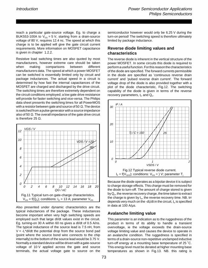
Introduction Power Semiconductor ApplicationsPhilips Semiconductors
reach a particular gate-source voltage. Eg. to charge aBUK553-100A to VGS = 5 V, starting from a drain-sourcevoltage of 80 V, requires 12.4 nc. The speed at which thischarge is to be applied will give the gate circuit currentrequirements. More information on MOSFET capacitanceis given in chapter 1.2.2.
Resistive load switching times are also quoted by mostmanufacturers, however extreme care should be takenwhen making comparisons between differentmanufacturers data. The speed at which a power MOSFETcan be switched is essentially limited only by circuit andpackage inductances. The actual speed in a circuit isdetermined by how fast the internal capacitances of theMOSFET are charged and discharged by the drive circuit.The switching times are therefore extremely dependent onthe circuit conditions employed; a low gate drive resistancewill provide for faster switching and vice-versa. The Philipsdata sheet presents the switching times for all PowerMOSwith a resistor between gate and source of 50 Ω. The deviceis switched from apulse generator with a source impedancealso of 50 Ω. The overall impedance of the gate drive circuitis therefore 25 Ω.
Fig.11 Typical turn-on gate-charge characteristics.VGS = f(QG); conditions: ID = 13 A; parameter VDS
Also presented under dynamic characteristics are thetypical inductances of the package. These inductancesbecome important when very high switching speeds areemployed such that large dI/dt values exist in the circuit.Eg. turning-on 30 A within 60 ns gives a dI/dt of 0.5 A/ns.The typical inductance of the source lead is 7.5 nH, fromV = -L*dI/dt the potential drop from the source bond pad(point where the source bond wire connects to the chipinternally) to the bottom of the source lead would be 3.75 V.Normallya standarddevice will be driven with agate-sourcevoltage of 10 V applied across the gate and sourceterminals, the actual voltage gate to source on the
semiconductor however would only be 6.25 V during theturn-on period! The switching speed is therefore ultimatelylimited by package inductance.
Reverse diode limiting values andcharacteristicsThe reverse diode is inherent in the vertical structure of thepower MOSFET. In some circuits this diode is required toperformauseful function. For this reasonthe characteristicsof the diode are specified. The forward currents permissiblein the diode are specified as ’continuous reverse draincurrent’ and ’pulsed reverse drain current’. The forwardvoltage drop of the diode is also provided together with aplot of the diode characteristic, Fig.12. The switchingcapability of the diode is given in terms of the reverserecovery parameters, trr and Qrr.
Fig.12 Typical reverse diode current.IF = f(VSDS); conditions: VGS = ) V; parameter Tj
Because the diode operates as a bipolar device it is subjectto charge storage effects. This charge must be removed forthe diode to turn-off. The amount of charge stored is givenby Qrr, the reverse recovery charge, the time taken to extractthe charge is given by trr, the reverse recovery time. NB. trrdepends very much on the -dIf/dt in the circuit, trr is specifiedin data at 100 A/µs.
Avalanche limiting valueThis parameter is an indication as to the ruggedness of theproduct in terms of its ability to handle a transientovervoltage, ie the voltage exceeds the drain-sourcevoltage limiting value and causes the device to operate inan avalanche condition. The ruggedness is specified interms of a drain-source non-repetitive unclamped inductiveturn-off energy at a mounting base temperature of 25 ˚C.This energy level must be derated at higher mounting basetemperatures as shown in Fig.13. NB. this rating is
0 1 2
BUK553-100A
VSDS / V
30
20
10
0
IF / A
Tj / C = 150 25
0 2 4 6 8 10 12 14 16 18 20QG / nC
VGS / V12
10
8
6
4
2
0
VDS / V =20
80
BUK553-100
73

Introduction Power Semiconductor ApplicationsPhilips Semiconductors
non-repetitive which means the circuit should not bedesigned to force the PowerMOS repeatedly intoavalanche. This rating is only to permit the device to surviveif exceptional circuit conditions arise such that a transientovervoltage occurs.
The new generation of Philips Medium Voltage MOSFETsalso feature a repetitive ruggedness rating. This rating isspecified in terms of a drain-source repetitive unclampedinductive turn-off energy at a mounting base temperatureof25 ˚C, and indicates that the devices are able to withstandrepeated momentary excursions into avalanchebreakdown provided the maximum junction temperature isnot exceeded. (A more detailed explanation of Ruggednessis given in chapter 1.2.7.)
Fig.13. Normalised avalanche energy rating.WDSS% = f(Tmb); conditions: ID = 13 A
Safe Operating AreaA plot of the safe operating area is presented for everyPowerMOS type. Unlike bipolar transistors a PowerMOSexhibits no second breakdown mechanism. The safeoperating area is therefore simply defined from the powerdissipation that will cause the junction temperature to reachthe maximum permitted value.
Fig.14 shows the SOA for a BUK553-100. The area isbounded by the limiting drain source voltage, limitingcurrent values and a set of constant power curves forvarious pulse durations. The plots in data are all for amounting base temperature of 25 ˚C. The constant powercurves therefore represent the power that raises thejunction temperature by an amount Tjmax - Tmb, ie. 150 ˚Cfor a device with a limiting Tj of 175 ˚C and 125 ˚C for adevice with a limiting Tj of 150 ˚C. . Clearly in mostapplications the mounting base temperature will be higherthan 25 ˚C, the SOA would therefore need to be reduced.The maximum power curves are calculated very simply.
Fig.14 Safe operating area. Tmb = 25 ˚CID & IDM = f(VDS); IDM single pulse; parameter tp
The dc curve is based upon the thermal resistance junctiontomounting base (junction to heatsink in the caseof isolatedpackages), which is substituted into equation 1. The curvesforpulsed operation assumea single shot pulseand insteadof thermal resistance, a value for transient thermalimpedance is used. Transient thermal impedance issupplied as graphical data for each type, an example isshown in Fig.15. For calculation of the single shot powerdissipation capability, a value at the required pulse width isread from the D = 0 curve and substituted in to equation 2.(A more detailed explanation of transient thermalimpedance and how to use the curves can be found inchapter 7.)
Examples of how to calculate the maximum powerdissipation for a 1 ms pulse are shown below. Example 1calculates the maximum power assuming a Tj of 175 ˚C andTmb of 25 ˚C. This power equates to the 1 ms curve on theSOA plot of Fig.14. Example 2 illustrates how the powercapability is reduced if Tmb is greater than 25 ˚C.
Example 1: 1 ms pulse at 25 ˚C for a BUK553-100A
Zth = 0.32 K/W, Tjmax = 175 ˚C, Tmb = 25 ˚C
1 100VDS / V
ID / A100
10
1
0.1
10 us
100 us
1 ms
10 ms
RDS(ON) =
VDS/ID
100 ms DC
tp =
BUK553-100
10
B
A
20 40 60 80 100 120 140 160 180Tmb / C
120
110
100
90
80
70
60
50
40
30
20
10
0
WDSS%
Ptot (dc) =Tjmax − Tmb
Rthj − mb
1
Ptot (pulse) =Tjmax − Tmb
Zthj − mb
2
74

Introduction Power Semiconductor ApplicationsPhilips Semiconductors
Fig.15 Transient thermal impedance.Zthj-mb = f(t); parameter D = tp/T
The 469 W line is observed on Fig.13, (4.69 A @ 100 V and15.6 A @ 30 V etc)
Example 2: 1 ms pulse at 75 ˚C for a BUK553-100A
Zth = 0.32 K/W, Tjmax = 175 ˚C, Tmb = 75 ˚C
Therefore with a mounting base temperature of 75 ˚C themaximum permissible power dissipation is reduced by onethird compared with the 25 ˚C value on the SOA plot.
Calculating CurrentsThe current ratings quoted in the data sheet are deriveddirectly from the maximum power dissipation.
substituting for Ptot from equation 1
To calculate a more realistic current it is necessary toreplace Tjmax in equation 4 with the desired operatingjunction temperature and Tmb with a realistic working value.It is generally recommended that devices are not operatedcontinuously at Tjmax. For reasons of long term reliability,125 ˚C is a more suitable junction operating temperature.A value of Tmb between 75 ˚C and 110 ˚C is also a moretypical figure.
As an example a BUK553-100A is quoted as having a dccurrent rating of 13 A. Assuming a Tmb of 100 ˚C andoperating Tj of 125 ˚C the device current is calculated asfollows:
From Fig.8
Rthj-mb = 2 K/W, using equation 4
The device could therefore conduct 6.3 A under theseconditions which equates to a 12.5 W power dissipation.
Conclusions
The most important information presented in the data sheetis the on-resistance and the maximum voltagedrain-source. Current values and maximum powerdissipation values should be viewed carefully since theyare only achievable if the mounting base temperature isheld to 25 ˚C. Switching times are applicable only for thespecific conditions described in the data sheet, whenmaking comparisons between devices from differentmanufacturers, particular attention should be paid to theseconditions.
ID(@Tmb) =
Tjmax − Tmb
Rthj − mb ⋅ RDS(ON)(@Tjmax)
1
2
4
1E-07 1E-05 1E-03 1E-01 1E+01t / s
Zth j-mb / (K/W)1E+01
1E+00
1E-01
1E-02
1E-03
0
0.5
0.20.1
0.05
0.02
BUKx53-lv
D = tp tp
T
TP
t
D
D =
RDS(ON)(@125oC) = 1.75⋅ RDS(ON)(@25oC) = 1.75⋅ 0.18= 0.315ΩPmax(1ms pulse) =
175− 250.32
= 469W
ID =
252 ⋅ 0.315
1
2
= 6.3A
Pmax(1ms pulse) =175− 75
0.32= 312W
ID(@Tmb)2 ⋅ RDS(ON)(@Tjmax) = Ptot 3
75

Introduction Power Semiconductor ApplicationsPhilips Semiconductors
High Voltage Bipolar Transistor
77

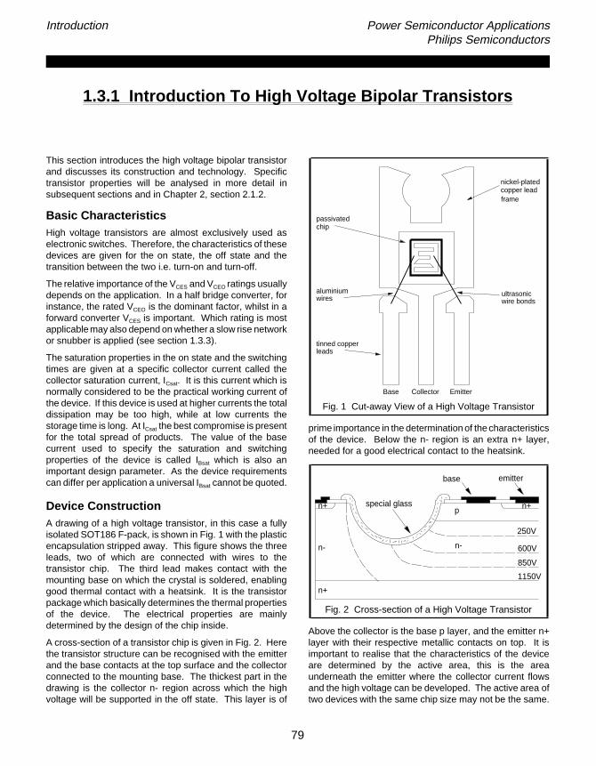
Introduction Power Semiconductor ApplicationsPhilips Semiconductors
1.3.1 Introduction To High Voltage Bipolar Transistors
This section introduces the high voltage bipolar transistorand discusses its construction and technology. Specifictransistor properties will be analysed in more detail insubsequent sections and in Chapter 2, section 2.1.2.
Basic CharacteristicsHigh voltage transistors are almost exclusively used aselectronic switches. Therefore, the characteristics of thesedevices are given for the on state, the off state and thetransition between the two i.e. turn-on and turn-off.
The relative importance of the VCES and VCEO ratings usuallydepends on the application. In a half bridge converter, forinstance, the rated VCEO is the dominant factor, whilst in aforward converter VCES is important. Which rating is mostapplicable may also depend on whether a slow rise networkor snubber is applied (see section 1.3.3).
The saturation properties in the on state and the switchingtimes are given at a specific collector current called thecollector saturation current, ICsat. It is this current which isnormally considered to be the practical working current ofthe device. If this device is used at higher currents the totaldissipation may be too high, while at low currents thestorage time is long. At ICsat the best compromise is presentfor the total spread of products. The value of the basecurrent used to specify the saturation and switchingproperties of the device is called IBsat which is also animportant design parameter. As the device requirementscan differ per application a universal IBsat cannot be quoted.
Device ConstructionA drawing of a high voltage transistor, in this case a fullyisolated SOT186 F-pack, is shown in Fig. 1 with the plasticencapsulation stripped away. This figure shows the threeleads, two of which are connected with wires to thetransistor chip. The third lead makes contact with themounting base on which the crystal is soldered, enablinggood thermal contact with a heatsink. It is the transistorpackage which basically determines the thermal propertiesof the device. The electrical properties are mainlydetermined by the design of the chip inside.
A cross-section of a transistor chip is given in Fig. 2. Herethe transistor structure can be recognised with the emitterand the base contacts at the top surface and the collectorconnected to the mounting base. The thickest part in thedrawing is the collector n- region across which the highvoltage will be supported in the off state. This layer is of
Fig. 1 Cut-away View of a High Voltage Transistor
prime importance in the determination of the characteristicsof the device. Below the n- region is an extra n+ layer,needed for a good electrical contact to the heatsink.
Fig. 2 Cross-section of a High Voltage Transistor
Above the collector is the base p layer, and the emitter n+layer with their respective metallic contacts on top. It isimportant to realise that the characteristics of the deviceare determined by the active area, this is the areaunderneath the emitter where the collector current flowsand the high voltage can be developed. The active area oftwo devices with the same chip size may not be the same.
nickel-platedcopper leadframe
passivatedchip
aluminiumwires
tinned copperleads
ultrasonicwire bonds
Base Collector Emitter
base emitter
250V
600V
850V
1150V
n-
n+
n+ p n+
n-
special glass
79
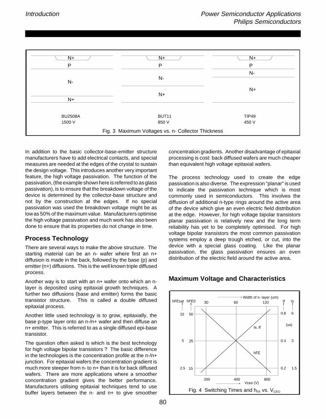
Introduction Power Semiconductor ApplicationsPhilips Semiconductors
Fig. 3 Maximum Voltages vs. n- Collector Thickness
N+
P
N-
N+
N+
P
N-
N+
N+
P
N-
N+
TIP49450 V
BUT11850 V
BU2508A1500 V
In addition to the basic collector-base-emitter structuremanufacturers have to add electrical contacts, and specialmeasures are needed at the edges of the crystal to sustainthe design voltage. This introduces another very importantfeature, the high voltage passivation. The function of thepassivation, (theexample shown here is referred to as glasspassivation), is to ensure that the breakdown voltage of thedevice is determined by the collector-base structure andnot by the construction at the edges. If no specialpassivation was used the breakdown voltage might be aslow as 50% of the maximum value. Manufacturers optimisethe high voltage passivation and much work has also beendone to ensure that its properties do not change in time.
Process TechnologyThere are several ways to make the above structure. Thestarting material can be an n- wafer where first an n+diffusion is made in the back, followed by the base (p) andemitter (n+) diffusions. This is the well known triple diffusedprocess.
Another way is to start with an n+ wafer onto which an n-layer is deposited using epitaxial growth techniques. Afurther two diffusions (base and emitter) forms the basictransistor structure. This is called a double diffusedepitaxial process.
Another little used technology is to grow, epitaxially, thebase p-type layer onto an n-/n+ wafer and then diffuse ann+ emitter. This is referred to as a single diffused epi-basetransistor.
The question often asked is which is the best technologyfor high voltage bipolar transistors ? The basic differencein the technologies is the concentration profile at the n-/n+junction. For epitaxial wafers the concentration gradient ismuch more steeper from n- to n+ than it is for back diffusedwafers. There are more applications where a smootherconcentration gradient gives the better performance.Manufacturers utilising epitaxial techniques tend to usebuffer layers between the n- and n+ to give smoother
concentration gradients. Another disadvantage of epitaxialprocessing is cost: back diffused wafers are much cheaperthan equivalent high voltage epitaxial wafers.
The process technology used to create the edgepassivation is also diverse. The expression "planar" is usedto indicate the passivation technique which is mostcommonly used in semiconductors. This involves thediffusion of additional n-type rings around the active areaof the device which give an even electric field distributionat the edge. However, for high voltage bipolar transistorsplanar passivation is relatively new and the long termreliability has yet to be completely optimised. For highvoltage bipolar transistors the most common passivationsystems employ a deep trough etched, or cut, into thedevice with a special glass coating. Like the planarpassivation, the glass passivation ensures an evendistribution of the electric field around the active area.
Maximum Voltage and Characteristics
Fig. 4 Switching Times and hFE vs. VCEO
200 400 800
15
25
5010
5
2.5
30 60 120hFEsat hFE0Width of n- layer (um)
0.8
0.4
0.2 1.5
3
6
tf ts
Vceo (V)
(us)
hFE
ts, tf
80

Introduction Power Semiconductor ApplicationsPhilips Semiconductors
High voltage and low voltage transistors differ primarily inthe thickness and resistivity of the n- layer. As the thicknessand resistivity of this layer is increased, the breakdownvoltage goes up. The difference over the range of Philipshigh voltage transistors of different voltages is illustrated inFig. 3. The TIP49 has a VCBO = 450 V, the BUT11 has aVCES = 850 V, while the BU2508A can be used up tovoltages of 1500 V.
The penalty for increasing the n- layer is a decrease in highcurrent hFE and an in switching times. The graph in Fig. 4points this out by giving both switching times and hFE as afunctionof the breakdown voltage. The values given shouldbe used as a guide to illustrate the effect. The effect canbe compensated for by having a bigger chip.
Applications of High Voltage TransistorsHigh voltage transistors are mainly used as the powerswitch in energy conversion systems. What is common to
all thesesystems, is thatacurrent flows through an inductor,thus storing energy in its core. When the current isinterrupted by turning off the power switch, the energy mustbe transferred one way or another. Very often the energyis converted into an electrical output e.g. in switched modepower supplies and battery chargers.
Two special applications are electronic fluorescent lampballasts and horizontal deflection of the electron beam inTV’sand monitors. In the ballast,an ac voltage is generatedto deliver energy to a fluorescent lamp. In the TV andmonitor a sawtooth current in the deflection coil sweeps thebeam across the screen from left to right and back again ina much shorter blanking, or flyback, period
Other ways to transfer the energy are ac and dc motorcontrol where the output is delivered as movement, orinduction heating where the output is delivered in the formof heat.
81


Introduction Power Semiconductor ApplicationsPhilips Semiconductors
1.3.2 Effects of Base Drive on Switching Times
Introduction
The switching processes that take place within a highvoltage transistor are quite different from those in a smallsignal transistor. This section describes, figuratively, whathappens within high voltage transistors under various basedrive conditions. After an analysis of the charges that arepresent in a high voltage transistor, the switch-off processis described. Then comparisons are made of switching forvarious forward and reverse base drive conditions. Afundamental knowledge of basic semiconductor physics isassumed.
Charge distribution within a transistor
An off-state transistor has no excess charge, but to enabletransistor conduction in the on-state excess charge buildup within the device takes place. There are three distinctcharge distributions to consider that control the currentthrough the device, see Fig. 1. These charge distributionsare influenced by the level of collector-emitter bias, VCE,and collector current, IC, as shown in Fig. 2.
Forward biasing the base-emitter (BE) junction causes adepletion layer to form across the junction. As the biasexceeds the potential energy barrier (work function) for thatjunction, current will flow. Electrons will flow out of theemitter into the base and out of the base contact. For highvoltage transistors the level of BE bias is much in excessof the forward bias for a small signal transistor. The biasgenerates free electron-hole pairs in the base-emitterleading to a concentration of electrons in the base in excessof the residualhole concentration. This produces an excesscharge in the base, Qb, concentrated underneath theemitter.
Fig. 1. On-state Charge Flow
Not only is there an excess charge in the base near theemitter junction but the injection and base width ensure thatthis excess charge is also present at the collector junction.Applying a load in series with the collector and a dc supplybetween load and emitter will trigger some sort of collectorcurrent, IC. The level of IC is dependent on the base current,IB, the load and supply voltage. For a certain IB, low voltagesupply and high impedance load there will be a small IC. Asthe supply voltage rises and/or the load impedance falls soIC will rise. As IC rises so the collector-emitter voltage, VCE,falls. The IC is composed mainly of the excess emitterelectrons that reach the base-collector junction (BC). Thiselectron concentration will continue into the collectorinducing an excess charge in the collector, Qc.
The concentration of electrons decreases only slightly fromthe emitter-base junction to some way into the collector. Ineffect, the base width extends into the collector. DecreasingVCE below VBE causes the BC junction to become forwardbiased throughout. This creates a path for electrons fromthe collector to be driven back into the base and out of thebase contact. This electron flow is in direct opposition tothe established IC. With no change in base drive, theultimate effect is a reduction in IC. This is the classical‘saturation’ region of transistor operation. As VCE falls sothe BC forward bias increases leading to an excess ofelectrons at the depletion layer edge in the collectorbeneath the base contact. This concentration of electronsleads to an excess charge, Qd.
The charge flows and excess charges Qb, Qc and Qd areshown in Fig. 1. An example of the excess chargedistributions for fixed IC and IB are shown in Fig. 2.
Fig. 2. On-state Charge Distribution (example)
The switching process of a transistorRemoving the bias voltage, VBE, will cause the electron-holepairs to recombine and the excess charge regions todisappear. Allowing this to happen just by removing VBE
QQd
Qc
Qb
Vce (V)
Ic = 5 A
Ib = 1 A
B E B
Qd Qc
QbP
N+
N-
N+
C
83

Introduction Power Semiconductor ApplicationsPhilips Semiconductors
takes a long time so usually turn-off is assisted in someway. It is common practice to apply a negative bias(typically 5V) to the base, via a resistor and/or inductor,inducing a negative current that draws the charge out ofthe transistor. In the sequence that follows, four phases ofturn-off can be distinguished (see Fig. 3).
1. First the applied negative bias tries to force a negativebias across the BC junction. The BC electron flow nowstops and the charge Qd dissipates as the bias now causesthe base holes out through the base contact and thecollector electrons back into the bulk collector. When theBC was forward biased this current had the effect ofreducing the total collector current, so now the negative VBE
can cause the total collector current to increase (this alsodependson the load). Although the base hasbeen switchedoff the load current is maintained by the stored chargeeffects; this is called the transistor storage time, ts.
During this stage the applied negative bias appears as apositive VBE at the device terminals as the internal chargedistributions create an effective battery voltage. Depletingthe charge, of course, lowers this effective battery voltage.
2. The next phase produces a reduction in both Qb, Qcand, consequently, IC. The BC junction is no longer forwardbiased and Qd has dissipated to provide the negative basecurrent. The inductance in series in the base path requiresacontinuation in the base current. The injection of electronsinto the base opposes the established electron flow fromemitter to collector via the base. At first the opposingelectron flows cancel at the edge of the emitter nearest thebase contacts. This reduces both Qb and Qc in this region.Qband Qc become concentrated in the centre of the emitterarea. The decrease in IC is called the fall time, tf.
3. Now there is an extra resistance to the negative basecurrent as the electrons flow through the base under theemitter area. This increase in resistance limits the increasein amplitude of the negative base current. As Qb and Qcreduce further so the resistance increases and the negativebase current reaches its maximum value.
As Qb and Qc tend to zero the series inductance ensuresthat negative base current must be continued by othermeans. The actual mechanism is by avalanche breakdownof the base-emitter junction. This now induces a negativeVBE which is larger than the bias resulting in a reverse inpolarity of the voltage across the inductance. This in turntriggers a positive rate of change in base current. Thenegative base current now quickly rises to zero while thebase-emitter junction is in avalanche breakdown.Avalanche breakdown ceases when the base current tendsto zero and the VBE becomes equal to the bias voltage. Fig. 3. Phases during turn-off
B E B
Qd Qc
QbP
N+
N-
N+
C
B E B
Qc
QbP
N+
N-
N+
C
B E B
P
N+
N-
N+
C
0Qb
Qc 0
B E B
P
N+
N-
N+
C
Qr
84

Introduction Power Semiconductor ApplicationsPhilips Semiconductors
4. If a very small series base inductor is used with the 5Vreverse bias then the base current will have a very fast rateof change. This will speed up the phases 1 to 3 and,therefore, the switching times of the transistor. However,there is a point when reducing the inductor furtherintroduces another phase to the turn-off process. Highreverse base currents will draw the charges out closest tothe base contact and leave a residual charge trapped deepin the collector regions furthest away from the base. Thischarge, Qr, must be removed before the transistor returnsfully to the off-state. This is detected as a tail to IC at theend of turn-off with a corresponding tail to the base currentas it tends to zero.
The switching waveforms for a BUT11 in a forwardconverter are given in Fig. 4 where the four phases caneasily be recognised. (Because of the small base coil usedboth phases in the fall time appear clearly!).
1 - Removal of Qd until t ≈ 0.7 µs ts
2 - Qc and Qb decrease until t ≈ 1.7 µs ts
3 - Removal of Qb and Qc until t ≈ 1.75 µs tf
4 - Removal of Qr until t ≈ 1.85 µs tf
Note the course of VBE: first the decrease in voltage due tothe base resistance during current contraction and second(because a base coil has been used) the value of VBE isclamped by the emitter-base breakdown voltage of thetransistor. It should be remembered that becausebreakdown takes place near the surface and not in theactive region no harm comes to the transistor.
Fig. 4. BUT11 waveforms at turn-off
The influence of forward drive on storedchargeFig. 5 shows how, for a transistor in the on-state, at a fixedvalue of IC and IB the three charges Qb, Qc and Qd dependupon VCE. The base charge, Qb, is independent of VCE, itprimarily depends upon VBE. For normal base drive
conditions, a satisfactory value for VCEsat is obtained,indicated by N in Fig. 5, and moderate values for Qc andQd result.
Fig. 5. Charges as a function of VCE
With the transistor operating in the active region, forVCE ≥ 1V, there will be a charge Qc but no charge Qd. Thisis indicated by D in Fig. 5. At the other extreme, with thetransistoroperating in the saturation region Qcwill be higherand Qd will be higher than Qc. This is indicated by O inFig. 5. In this condition there are more excess electron-holepairs to recombine at switch off.
Increasing IB causes Qb to increase. Also, for a given IC,Qc and Qd will be higher as VCE reduces. Therefore, for agiven IC, the storedcharge in the transistor can be controlledby the level of IB. If the IB is too low the VCE will be high withlow Qc and zero Qd, as D in Fig. 5. This condition is calledunderdrive . If the IB is too high the VCE will be low with highQc and Qd, as O in Fig. 5. This condition is calledoverdrive . The overdrive condition (high forward drive)gives high stored charge and the underdrive condition (lowforward drive) gives low stored charge.
Deep-hole storage
As the high free electron concentration extends into thebase and collector regions ther must be an equivalent holeconcentration. Fig. 6 shows results obtained from acomputer model which illustrates charge storage as afunction of VCE. Here the hole density, p(x), is given as afunction of depth inside the active area; the doping profileis also indicated. It can be seen that overdrive, O, causesholes to be stored deep in the collector at the collector -substrate junction known as "deep-hole storage", this is themain reason for the increase in residual charge, Qr.
QQd
Qc
Qb
0.2 0.5 1.0 Vce (V)
O N D
Ic
Vce
Ib Vbe
1 A/div
1 A/div
200 V/div
5 V/div
0.5 us/div
85

Introduction Power Semiconductor ApplicationsPhilips Semiconductors
During overdrive not only Qd becomes very big but alsoholes are stored far away from the junction: this thus leadsnot only to a longer storage time, but also to a large Qrresulting in tails in the turn-off current.
Fig. 6. Deep hole storage in the collector region
Desaturation networksA desaturation network, as shown in Fig. 7, limits the storedcharge in the transistor and, hence, aids switching. Theseries base diode, D1 means that the applied drive voltagenow has to be VBE plus the VF of D1. The anti-parallel diode,D2 is necessary for the negative IB at turn-off. As VCE
reduces below VBE + VF so the external BC diode, D3,becomes forward biased. D3 now conducts any furtherincrease in drive current away from the base and into thecollector. Transistor saturation is avoided.
With a desaturation network the charge Qd equals zero andthe charge Qc is minimised. When examining thedistribution of the charge in the collector region (see Fig. 6)it can be seen that deep hole storage does not appear.Desaturation networks are a common technique forreducing switching times.
It should be realised that there is a drawback attached tooperating out of saturation: increased dissipation during theon-state. Base drive design often requires a trade-offbetween switching and on-state losses.
Fig. 7. Desaturation network(Baker clamp)
Breakdown voltage vs. switching times
For a higher breakdown voltage transistor the n- layer (seeFig. 1) will be thicker and of higher resistivity (ie a lowerdonor atom concentration). This means that whencomparing identical devices the values for Qd and Qc willbe higher, for a given IC, in the device with the higherbreakdown voltage.
In general:
- the higher BVCEO the larger Qd and Qc will be;
- during overdrive Qd is very high and there is a chargelocated deep in the collector region (deep hole storage);
- when desaturated Qd equals zero and there is no deephole storage: Qc is minimised for the IC.
Turn-off conditions
Various ways of turning off a high voltage transistor areused but the base should always be switched to a negativesupply via an appropriate impedance. If this is not done,(ie turn-off is attempted by simply interrupting the basecurrent), very long storage times result and the collectorvoltage increases, while the collector current falls onlyslowly. A very high dissipation and thus a short lifetime ofthe transistor are the result. The charges must be removedusing a negative base current.
a) Hard turn-off
The technique widely used, especially for low voltagetransistors, is to switch directly to a negative voltage, (seeFig. 8a). In the absence of a negative supply, this can beachieved with an appropriate R-C network (Fig. 8b). Alsoapplying an "emitter-drive" (Fig. 8c) with a large basecapacitor in fact is identical to hard-turn-off.
The main drawback for high voltage transistors is that thebase charge Qb is removed too quickly, leaving a highresidual charge. This leads to current tails (long fall times)and high dissipation. It depends upon what state thetransistor is in (overdriven or desaturated),whether this wayof turn-off is best. It also depends upon the kind of transistorthat must be switched off. If it is a lower voltage transistor(BVCEO ≤ 200V) then this will work very well because thecharges Qc and Qd will be rather low. For transistors witha higher breakdown voltage, hard turn-off will yield theshortest storage time at the cost, however, of higher turn-offdissipation (longer tf).
b) Smooth turn-off
To properly turn-off a high voltage transistor a storage timetominimiseQd andQc is required,and thena large negativebase current to give a short fall time.
0 80 1604020 60 120100 140
20
10
12
14
16
18
10
10
10
10
10
10
Vce = 1 V 0.5 V 0.2 V
p(x) at J = 140 A / cm2
p(x)
x (um)
E BC
D N O
B
C
E
D3
D1
D2
86
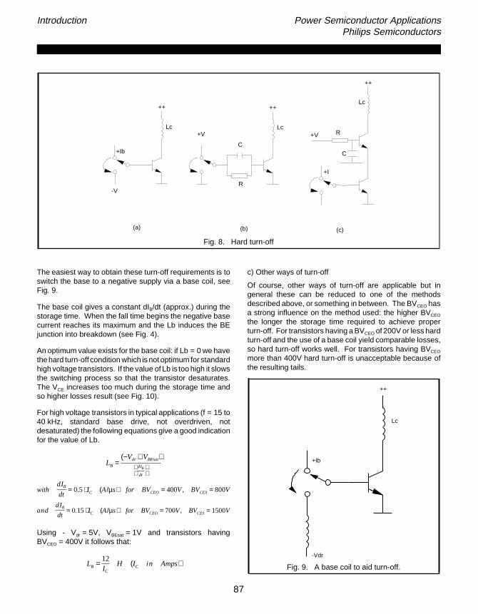
Introduction Power Semiconductor ApplicationsPhilips Semiconductors
Fig. 8. Hard turn-off
-V
+Ib
++
Lc
++
Lc+V
C
R
++
Lc
+V
+I
R
C
(a) (b) (c)
The easiest way to obtain these turn-off requirements is toswitch the base to a negative supply via a base coil, seeFig. 9.
The base coil gives a constant dIB/dt (approx.) during thestorage time. When the fall time begins the negative basecurrent reaches its maximum and the Lb induces the BEjunction into breakdown (see Fig. 4).
An optimum value exists for the base coil: if Lb = 0 we havethe hard turn-off condition which is not optimum for standardhigh voltage transistors. If the value of Lb is too high it slowsthe switching process so that the transistor desaturates.The VCE increases too much during the storage time andso higher losses result (see Fig. 10).
For high voltage transistors in typical applications (f = 15 to40 kHz, standard base drive, not overdriven, notdesaturated) the following equations give a good indicationfor the value of Lb.
Using - Vdr = 5V, VBEsat = 1V and transistors havingBVCEO = 400V it follows that:
c) Other ways of turn-off
Of course, other ways of turn-off are applicable but ingeneral these can be reduced to one of the methodsdescribed above, or something in between. The BVCEO hasa strong influence on the method used: the higher BVCEO
the longer the storage time required to achieve properturn-off. For transistors having a BVCEO of 200V or less hardturn-off and the use of a base coil yield comparable losses,so hard turn-off works well. For transistors having BVCEO
more than 400V hard turn-off is unacceptable because ofthe resulting tails.
Fig. 9. A base coil to aid turn-off.
+Ib
++
Lc
-Vdr
LB =(−Vdr + VBEsat)
dIB
dt
withdIBdt
≈ 0.5⋅ IC (A/µs) for BVCEO = 400V, BVCES = 800V
anddIBdt
≈ 0.15⋅ IC (A/µs) for BVCEO = 700V, BVCES = 1500V
LB =12IC
H (IC in Amps)
87

Introduction Power Semiconductor ApplicationsPhilips Semiconductors
Fig. 10. Variations of Lb on IC and VCE waveforms at turn-off
Ic Vce Ic Vce IcVce
Lb = 0 Lb = opt Lb > Lb opt
Turn-off for various forward driveconditionsUsing the BUT11 as an example, turn-off characteristicsare discussed for optimum drive, underdrive and overdrivewith hard and smooth turn-off.
a) Optimum driveThe optimum IB and Lb for a range of IC is given in Fig. 11for the BUT11. The IB referred to is IBend which is the valueof IB at the end of the on-state of the applied base drivesignal. In most applications during the on-state the IB willnot be constant, hence the term IBend rather than IBon. Foroptimumdrive the level of IBend increases with IC. For smoothturn-off the level of Lb decreases with increasing IC.
Fig. 11. IBend and Lb for the BUT11
Deviations from Fig. 11 will generally lead to higher powerdissipation. If a short storage time is a must in a certainapplication then Lb can be reduced but this will lead tolonger fall times and current tails.
With hard turn-off IB reaches its peak negative value as allthe charge is removed from the base. For continuity thiscurrentmust be sourced fromelsewhere. It hasbeen shownthat the BE junction now avalanches, giving instantaneouscontinuity followed by a positive dIB/dt. However, for hardturn-off the current is sourced by the residual collectorcharge without BE avalanche, see Fig. 12. The smallnegative VBE ensures a long tail to IC and IB.
b) Underdrive (Desaturated drive)As has been indicated previously, desaturating, orunderdriving, a transistor results in less internal charge. Qdwill be zero and Qc is low and located near the junction.
If the application requires such a drive then steps shouldbe taken to optimise the characteristics. One simple wayof obtaining underdrive is to increase the series baseresistance with smooth turn-off. The same effect can beachieved with optimum IBend and a base coil having half thevalue used for optimum drive, ie hard turn-off. Bothmethods give shorter ts and tf. For 400V BVCEO devices (likethe Philips BUT range) such a harder turn-off can lead toreasonable results.
Fig. 13 compares the use of the optimum base coil withhard turn-off for an undriven BUT11. For underdrive thefinal IC is less and hence the collector charge is less.Therefore, underdrive and hard turn-off gives less of a tailthan for a higher IBend. Underdrive with smooth turn-off giveslonger ts but reduced losses.
c) OverdriveWhen a transistor is severely overdriven the BC charge,Qd, becomes so large that a considerable tail will resulteven with smooth turn-off. In general, deliberatelydesigning a drive circuit to overdrive a transistor is not done:it has no real value. However, most circuits do have variablecollector loads which can result in extreme conditions whenthe circuit is required to operate with the transistor inoverdrive.
88
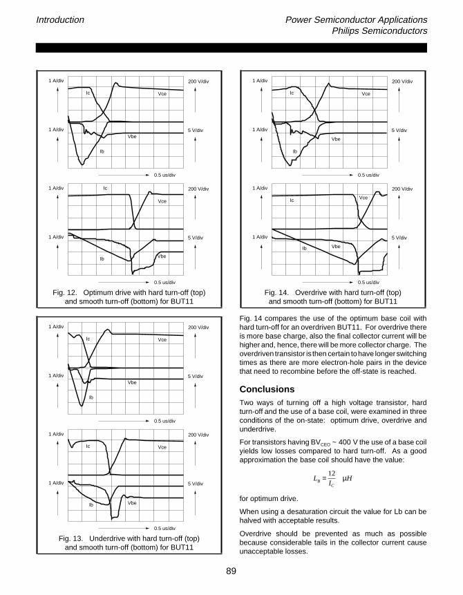
Introduction Power Semiconductor ApplicationsPhilips Semiconductors
Fig. 12. Optimum drive with hard turn-off (top)and smooth turn-off (bottom) for BUT11
Fig. 13. Underdrive with hard turn-off (top)and smooth turn-off (bottom) for BUT11
Fig. 14. Overdrive with hard turn-off (top)and smooth turn-off (bottom) for BUT11
Fig. 14 compares the use of the optimum base coil withhard turn-off for an overdriven BUT11. For overdrive thereis more base charge, also the final collector current will behigher and, hence, there will be more collector charge. Theoverdriven transistor is then certain tohave longerswitchingtimes as there are more electron-hole pairs in the devicethat need to recombine before the off-state is reached.
ConclusionsTwo ways of turning off a high voltage transistor, hardturn-off and the use of a base coil, were examined in threeconditions of the on-state: optimum drive, overdrive andunderdrive.
For transistors having BVCEO ~ 400 V the use of a base coilyields low losses compared to hard turn-off. As a goodapproximation the base coil should have the value:
for optimum drive.
When using a desaturation circuit the value for Lb can behalved with acceptable results.
Overdrive should be prevented as much as possiblebecause considerable tails in the collector current causeunacceptable losses.
Ic Vce
Ib
Vbe
1 A/div
1 A/div
200 V/div
5 V/div
0.5 us/div
Ic Vce
Ib
Vbe
1 A/div
1 A/div
200 V/div
5 V/div
0.5 us/div
Ic
Vce
Ib Vbe
1 A/div
1 A/div
200 V/div
5 V/div
0.5 us/div
Ic Vce
Ib Vbe
1 A/div
1 A/div
200 V/div
5 V/div
0.5 us/div
Ic Vce
Ib
Vbe
1 A/div
1 A/div
200 V/div
5 V/div
0.5 us/div
Ic Vce
Ib Vbe
1 A/div
1 A/div
200 V/div
5 V/div
0.5 us/div
LB =12IC
µH
89

Introduction Power Semiconductor ApplicationsPhilips Semiconductors
1.3.3 Using High Voltage Bipolar Transistors
This section looks at some aspects of using high voltagebipolar transistors in switching circuits. It highlights pointssuchas switching, both turn-on and turn-off, Safe OperatingAreas and the need for snubber circuits. Base drive designcurves for the BUT11, BUW12 and BUW13 are discussedunder ’Application Information’ at the end of this section.
Transistor switching: turn-on
To make optimum use of today’s high voltage transistors,one should carefully choose the correct value for both thepositive base current when the transistor is on and thenegative base current when the device is switched off (seeApplication Information section).
When a transistor is in the off-state, there are no carriersin the thick n- collector, effectively there is a resistor with arelatively high value in the collector. To obtain a lowon-state voltage, a base current is applied such that thecollector area is quickly filled with electron - hole pairscausing the collector resistance to decrease. In thetransition time, the so called turn-on time, the voltage andcurrent may both be high, especially in forward converters,and high turn-on losses may result. Initially, all the carriersin the collector will be delivered via the base contact and,therefore, the base current waveform should have a peakat the beginning. In this way the carriers quickly fill thecollector area so the voltage is lower and the lossesdecrease.
In flyback converters the current to be turned on is normallylow, but in forward converters this current is normally high.Thecollector current, IC, reaches its on-state value in ashorttime which is normally determined by the leakageinductance of the transformer.
Fig. 1 Turn-on of a high voltage bipolar transistor
In Fig. 1 the characteristic ‘hump’ which often occurs atturn-on in forward converters due to the effect of thecollector series resistance is observed.
The turn-on losses are strongly dependent on the value ofthe leakage inductance and the applied base drive. It isgenerally advised to apply a high initial +IB for a short timein order to minimise turn on losses.
A deeper analysis can be found in sections 1.3.2, 2.1.2 and2.1.3. Turn on losses are generally low for flybackconverters but are the most important factor in forwardconverter types.
Turn-off of high voltage transistorsAll charge stored in the collector when the transistor is onshould be removed again at turn-off. To ensure a quickturn-offa negative base current is applied. The time neededto remove the base - collector charge is called the storagetime. A short storage time is needed to minimise problemswithin the control loop in SMPS and deflection applications.
Fig. 2 Effects of -IB on turn-off
Care is needed to implement the optimum drive. Firstoverdriveshould be prevented by keeping+IB to aminimum.Overdrive results in current tails and long storage times.But, decreasing IB too much results in high on-state losses.
Second, the negative base current should be chosencarefully. A small negative base current (-IB) will give a longstorage time and a high VCEsat at the end of the storage time,while the current is still high. As a consequence, the turn-offlosses will be high. If, however, a large negative basecurrent is used, the danger exists that tails will occur in thecollector current, again resulting in high losses. There isan optimum as shown in Fig. 2.
A circuit which is worth considering, especially for higherfrequencies, is the Baker Clamp or desaturation circuit.This circuit prevents saturation of the transistor and, hence,faster switching times are achieved.
Ic Vce Ic Vce IcVce
-Ib is too high -Ib is optimum -Ib is too low
Ic
Vce
Ic = 1 A/div
Vce = 50 V/div
91

Introduction Power Semiconductor ApplicationsPhilips Semiconductors
The total losses depend on the base drive and the collectorcurrent. In Fig.3 the total losses are shown for a BUW133as a function of the positive base current, for both thesaturated and the desaturated case. Note that whendifferent conditions are being used the picture will change.The application defines the acceptable storage time whichthen determines the base drive requirements.
Fig. 3 BUW133 losses versus base drive
The total number of variables is too large to give uniquebase drive advice for each application. As a first hint thedevice data sheets give IC and IB values for VCEsat, VBEsat andswitching. However, it is more important to appreciate theways to influence base drive and the consequences of anon-optimised circuit.
For a flyback converter the best value of IBend to start withis about 2/3 of the IB value given in data for VCEsat and VBEsat.In this application the forward base current is proportionalto the collector current (triangular shaped waveforms) andthis IBend value will give low on-state losses and fastswitching.
The best turn-off base current depends on the breakdownvoltage of the transistor. As a guide, Table 1 givesreasonable values for the target storage time and may beused to begin optimising the base drive:
f (kHz) tp (µs) target ts (µs)
25 20 2.0
150 10 1.5
100 5 1.0
Table 1 Target ts for varying frequency and pulse width
The above table holds for transistors with a VCEOmax ratingof 400-450V and VCESmax between 850-1000V. Transistorswith higher voltages require longer storage times, eg.
transistors with VCEOmax = 700V and VCESmax = 1500V needa storage time which is approximately double the value inthe table.
A recommended way to control the storage time is byswitching the base to a negative voltage rail via a base coil.The leakage inductance of a driver transformer may serveas an excellent base coil. As a guide, the base coil shouldbe chosen such that the peak value of the negative basecurrent equals half the value of the collector current.
Specific problems and solutionsA high voltage transistor needs protection circuits to ensurethat the device will survive all the currents and voltages itwill see during its life in an application.
a) Over Current
Exceeding current ratings normally does not lead toimmediate transistor failure. In the case of a short circuit,the protection is normally fast enough for problems to beavoided. Most devices are capable of carrying very highcurrents for short periods of time. High currents will raisethe junction temperature and if Tjmax is exceeded thereliability of the device may be weakened.
b) Over Voltage
In contrast with over current, it is NOT allowed to exceedthe published voltage ratings for VCEO and VCES (or VCBO).In switching applications it is common for the base - emitterjunction to be taken into avalanche, this does not harm thedevice. For this reason VEBO limits are not given in data.
Exceeding VCEO and VCES causes high currents to flow invery small areas of the device. These currents may causeimmediate damage to the device in very short times(nanoseconds). So, even for very short times it is notallowed to have voltages above data for the device.
In reality VCEO and VCES are unlikely to occur in a circuit. IfVBE = 0V the there will probably still be a path between thebase and the emitter. In fact the situation is VCEX where Xis the impedance of this path. To cover for all values of X,the limit is X=∞, ie VCEO. For all VBE < 0V, ie VCEV, the limitcase is VBE = 0V, ie VCES.
If voltage transients that exceed the voltage limits aredetected then a snubber circuit may limit the voltage to asafe value. If the over voltage states last greater than afew µs a higher voltage device is required.
c) Forward Bias Safe Operating Areas (FBSOA)
The FBSOA is valid for positive values of VBE. There is atime limit to VCE - IC operating points beyond which devicefailure becomes a risk. At certain values of VCE and IC thereis a risk of secondary breakdown; this is likely to lead to theimmediate failure of the device. The FBSOA curve shouldonly be considered during drastic change sequences; forexample, start-up, s/c or o/c load.
With Baker Clamp
Saturated
100
200
300
400
500
600
700
Etot (uJ)
1 2 3 4
Ib (A)
Forward Converter
Ic = 10 A
92

Introduction Power Semiconductor ApplicationsPhilips Semiconductors
d) Reverse Bias Safe Operating Area (RBSOA)
The RBSOA is valid for negative values of VBE. Duringturn-off with an inductive load the VCE will rise as the IC falls.For each device type there is a VCE - IC boundary which, ifexceeded, will lead to the immediate failure of the device.To limit the VCE - IC path at turn-off snubber circuits are used,see Fig. 4.
Fig. 4 HVT with inductive load and typical snubber
At turn-off, as the VCE rises the diode starts conductingcharging the capacitor. The additional diode current meansthat the total load current does not decrease so fast atturn-off. This slower current tail in turn ensures a slowerVCE rise. The slower VCE rise takes the transistor througha safer VCE - IC path away from the limit, see Fig. 5.
As a handy guide, the snubber capacitor in a 20-40 kHzconverter is about 1nF for each 100W of throughput power(this is the power which is being transferred via thetransformer). This value may be reduced empirically asrequired.
Fig. 5 BUW13A RBSOA limitVCE - IC path with and without snubber
The following table may serve as a guide to the value ofdVCE/dt for some switching frequencies
f (kHz) 25 50 100
dVCE/dt 1 2 4(kV/µs)
Thesnubber resistor should be chosen so that the capacitorwill be discharged in the shortest occurring on-time of theswitch.
In some cases the losses in the snubber may beconsiderable. Clever designs exist to feed the energystored in the capacitor back into the supply capacitor, butthis is beyond the scope of this report.
5
10
15
20
200 400 600 800 1000
BUW13A
Ic
Vce
Without Snubber
With Snubber
Vs
Fig. 6 Transistor with maximum protection networks in SMPS circuit
R5C5 C4
D4
D5
D6
R4TR1
L6R6
D3 D1
D2
Lo
Co Vo
Vi
93

Introduction Power Semiconductor ApplicationsPhilips Semiconductors
d) Other protection networks
In Fig. 6 a "maximum protection" diagram is shown withvarious networks connected. R4, C4, and D4 form thesnubber to limit the rate of rise of VCE. The network withD5, R5 and C5 forms a "peak detector" to limit the peakVCE.
The inductor L6 serves to limit the rate of rise of IC whichmay be very high for some transformer designs. The slowerdIC/dt leads to considerably lower turn-on losses. Addedto L6 is a diode D6 and resistor R6, with values chosen sothat L6 loses its energy during the off-time of the powerswitch.
While the snubber is present in almost all SMPS circuitswhere transistors are used above VCEOmax, the dIC/dt limiteris only needed when the transformer leakage inductanceis extremely low. The peak detector is applied in circuitswhich have bad coupling between primary and secondarywindings.
Application InformationImportant design factors of SMPS circuits are the maximumpower losses, heatsink requirements and base driveconditions of the switching transistor. The power lossesare very dependent on the operating frequency, the
maximum collector current amplitude and shape.
The operating frequency is usually between 15 and 50 kHz.The collector current shape varies from rectangular in aforward converter to sawtooth in a flyback converter.
Examples of base drive and losses are given in Appendix 1for the BUT11, BUW12 and BUW13. In these figures ICM
represents the maximum repetitive peak collector current,which occurs during overload. The information is derivedfrom limit-case transistors at a mounting base temperatureof 100 ˚C under the following conditions (see also Fig. 7):
- collector current shape IC1 / ICM = 0.9- duty factor (tp / T) = 0.45- rate of rise of IC during turn-on = 4 A/µs- rate of rise VCE during turn-off = 1 kV/µs- reverse drive voltage during turn-off = 5 V- base current shape IB1 / IBe = 1.5
The required thermal resistance of the heatsink can becalculated from
To ensure thermal stability a maximum value of the ambienttemperature, Tamb, is assumed: Tamb ≤ 40˚C.
Rth(mb− amb) <100− Tamb
Ptot
K/W
Fig. 7 Relevant waveforms of the switching transistor in a forward SMPS.
Ic
Ic1
Icm
Vce
Ib
Vbe
Ib1Ib(end)
-Vdrive
T
tp
dIc/dt
0.9 Icm
0.1 Icm
t1 = 0.5 us
Vce(t1)
ts
tf
Turn-on Turn-off
94

Introduction Power Semiconductor ApplicationsPhilips Semiconductors
As a base coil is normally advised and a negative drivevoltage of -5V is rather common, the value for the base coil,LB, is given for these conditions. For other values of -Vdrive
(-3 to -7 volt) the base coil follows from:
Where LBnom is the value given in Appendix 1.
It should be noted, that this advice yields acceptable powerlosses for the whole spread in the product. It is not just fortypical products as is sometimes thought ! This isdemonstrated in Fig. 8, where limit and typical devices arecompared (worst-case saturation and worst-caseswitching).
It appears that the worst-case fall time devices have lossesP0 for IBend = (Ib adv) + 20%, while the saturationworst-casedevices have the same lossesat (Ib adv) - 20%.A typical device now has losses P1 at Ib adv, while theoptimum IBend for the typical case might yield losses P2 atan approximately 15% lower IBend (NB: this is not a rule, itis an example).
Fig. 8 Losses as a function of IBend
ConclusionTo avoid exceeding the RBSOA of an HVT, snubbers area requirement for most circuits. To minimise both switchingand on-state losses, particular attention should be given tothe design of the base drive circuit. It is generally advisedthat a high initial base current is applied for a short time tominimise turn-on loss. As a guide-line for turn-off, a basecoil should be chosen such that the peak value of thenegative base current equals half the value of the collectorcurrent.
-20% Ib adv +20% Ibe
w.c. (tf) typ. w.c. (sat)
P0
P1
P2
Ploss
LB = LBnom⋅(−Vdrive + 1)
6
95
Introduction Power Semiconductor ApplicationsPhilips Semiconductors
Appendix 1 Base Drive Design Graphs
BUT11 Base Drive Design Information
BUW12 Base Drive Design Information
BUW13 Base Drive Design Information
96

Introduction Power Semiconductor ApplicationsPhilips Semiconductors
1.3.4 Understanding The Data Sheet: High Voltage Transistors
Introduction
Being one of the most important switching devices inpresent day switched mode power supplies and other fastswitching applications, the high voltage transistor is acomponent with many aspects that designersdo not alwaysfully understand. In spite of its "age" and the variety ofpapersand publications by manufacturers andusers of highvoltage transistors, data sheets are somewhat limited in theinformation they give. This section deals with the datasheets of high voltage transistors and the background totheir properties. A more detailed look at the background totransistor specifications can be found in chapter 2.1.2.
Fig. 1 shows the cross section of a high voltage transistor.The active part of the transistor is highlighted (the areaunderneath the emitter) and it is this part of the silicon thatdetermines the primary properties of the device:breakdown voltages, hFE, switching times. All the addedparts can only make these properties worse: a badpassivation scheme can yield a much lower collector-basebreakdown voltage, too thin wires may seriously decreasethe current capability, a bad die bond (solder layer) leadsto a high thermal resistance leading to poor thermal fatiguebehaviour.
Fig. 1 Simplified cross section of an HVT
The Data Sheet
The data sheet of a high voltage transistor can specify -
* Limiting Values / Ratings: the maximum allowablecurrents through and voltages across terminals, as well astemperatures that must not be exceeded.
* Characteristics: describing properties in the on and offstate (static) as well as dynamic, both in words and infigures.
* SOA: Safe Operating Area both in forward and reversebiased conditions.
Data sheets are intended to be a means of presenting theessentials of a device and, at the same time, to give anoverview of the guaranteed specification points. This datais checked as a final measurement of the device andcustomers may wish to use it for their incoming inspection.For this reason the data is such that it can be inspectedrather easily in relatively simple test circuits. Thissomewhat application unfriendly way of presenting data isunavoidable if cheap devices are a must, and they are !
Each of the above mentioned items will now be discussedin more detail, in some instances parts of the data for aBUT11 will be used as an example. The BUT11 is intendedfor 3A applications and has a maximum VCES of 850V.
Limiting Values / Maximum RatingsThere is a significant difference between current andvoltage ratings. Exceeding voltage ratings can lead tobreakdown phenomena which are possibly destructivewithin fractions of a second. The avalanche effectsnormally take place within a very small volume and,therefore, only a little energy can be absorbed. Surgevoltages, that are sometimes allowed for othercomponents, are out of the question for high voltagetransistors.
There is, however, no reason to have a derating onvoltages: using the device up to its full voltage ratings - inworst case situations - is allowed. The life tests, carried outin Philips quality laboratories, clearly show that no voltagedegradation takes place and excellent reliability ismaintained.
From the above, it should be clear that the habit of deratingis not a good one. If, in a particular application, thecollector-emitter voltage never exceeds, say 800V, therequired device should be an 850V device not a 1500Vdevice. Higher voltage devices not only have lower hFE, butalso slower switching speeds and higher dissipation.
The rating for the emitter-base voltage is a special case:to allow a base coil to be used, the base-emitter diode maybe brought into breakdown; in some cases a -IBav is givento prevent excessive base-emitter dissipation. The onlyeffect of long term repetitive base-emitter avalanchebreakdown that has been observed is a slight decrease inhFE at very low values of collector current (approximately10% at ≤ 5mA); at higher currents the effects can beneglected completely.
N
P
N
mounting base = collector
bonding wire
glass passivation
active area solder
97

Introduction Power Semiconductor ApplicationsPhilips Semiconductors
The maximum value for VCEO is important if no snubber isapplied; it sets a firm boundary in applications with a veryfast rising collector voltage and a normal base drive (seealso section on SOA).
Currents above a certain value may be destructive if theylast long enough: bonding wires fuse due to excessiveheating. Therefore, short peak currents are allowed wellabove the rated ICsat with values up to five times this valuebeing published for ICM. Exceeding the published maximumtemperatures is not immediately destructive, but mayseriously affect the useful life of the device. It is well known,that the useful life of a semiconductor device doubles foreach 10K decrease in working junction temperature.Another factor that should be kept in mind is the thermalfatigue behaviour, which strongly depends on thedie-bonding technology used. Philips high voltage devicesare capable of 10,000 cycles with a temperature rise of 90Kwithout any degradation in performance.
This kind of consideration leads to the following advice:under worst case conditions the maximumcase-temperature should not exceed 115 ˚C for reliableoperation. This advice is valid regardless of the maximumtemperature being specified. Of course, for storage thepublished values remain valid.
The maximum total power dissipation Ptot is an industrystandard, but not very useful, parameter. It is the quotientof Tjmax - Tmb and Rth(j-mb) (Rth(j-mb) is the thermal resistancefrom junction to mounting base and Tmb is assumed to be25˚C). This implies a rather impractical infinite heatsink,kept at 25˚C !
Electrical CharacteristicsStatic parameters characterise leakage currents, hFE,saturation voltages; dynamic parameters and switchingtimes, but also include transition frequency and collectorcapacitance.
To start: ICsat, the collector saturation current, is that valueof the collector current where both saturation and switchingproperties of the devices are specified. ICsat is not acharacteristic that can be measured, but it is used as anindicationof the of the peak workingcurrent allowedthrougha device.
In the off-state various leakage currents are specified,however, these are of little use as they indicate the low levelof dissipation in the off state. Also a VCEOsust is specified,usually being equal to the max. VCEO. For switchingpurposes it is the RBSOA that is important (see nextsection).
In the on state the saturation voltages VCEsat and, to a lesserextent, VBEsat are important. VCEsat is an indication of thesaturation losses and VBEsat normally influences base drive.Sometimes worst case VCEsat is given as a function of bothIC and IB. It is not possible to precisely relate these curves
to a real circuit; in practice, currents and voltages will varyover the switching cycle. The dynamic performance isdifferent to the static performance. However, a reasonableindication can be obtained from these curves.
Both the transition frequency (fT) and the collectorcapacitance (Cc or Cob) are minor parameters relating to thedesign and processing technology used.
Switching times may be given in circuits with an inductiveor a resistive collector load. See Figs. 2a-b for simplifiedtest circuits and Figs. 3a-b for waveforms.
Fig. 2a Test circuit for resistive load
Fig. 2b Test circuit for inductive load
When comparing similar devices from differentmanufacturers one is confrontedwith a great variety of basedrive conditions. The positive base current (+IB) may bethe same as the one used in the VCEsat spec. but also lowervalues (up to 40% lower) or desaturation networks may beused, yielding better ts and tf values. The negative basedrive, -IB, may equal +IB or it may be twice this value, yieldinga shorter ts, and sometimes it is determined by switchingthe base to a negative voltage, possibly via a base coil.Altogether it is quite confusing and when comparingswitching times one should be well aware of all thedifferences!
tp
T
VCC
RL
RBT.U.T.0
VIM
LBIBon
-VBB
LC
T.U.T.
VCC
98
Introduction Power Semiconductor ApplicationsPhilips Semiconductors
Fig. 3a Waveforms for Resistive Switching.
Fig. 3b Waveforms for Inductive Switching.
As an example a BUT11 has been measured at IC = 3A ina resistive test circuit varying both +IB and -IB. The resultsin Table 1 show that it is possible to turn a normal transistorinto a super device by simple specmanship!
IC = 3 A ts (µs) tf (ns)
+IB = 0.6 A; -IB = 0.6 A 2.5 260(normal case)
+IB = 0.36 A; -IB = 0.72 A 1.6 210(underdriven)
+IB = 0.36 A; -VBE = -5 V 0.8 50(underdriven, hard turn-off)
Table 1 Switching times and base drive for the BUT11
The effect of base drive variations on storage and fall timesis given in Table 2. The reference is the condition that both+IB as well as -IB equals the value for IB given for the VCEsat
specification in the data sheet.
ts tf comments
+IB = ref. normal normal reference
+IB = 40% less ↓ ↓
Desaturated ↓ ↓
-IB = ref. normal normal reference
-IB = 2 x +IB ↓ ↓
Directly to -5 V ↓ ↑ with normalbase drive!
Directly to -5 V ↓ ↓ if underdriven
Via L to -5 V ↓ ↓
Table 2 Switching times and base drive variations.
The turn-on time is a parameter which only partiallycorrelates with dissipation as it is usually the behaviourdirectly after the turn-on time which appears to be mostsignificant. Both inductive and resistive load test circuitsare only partially useful, as resistive loads are seldom usedand very often some form of slow-rise network is used withinductive loads. Both circuits provide easy lab.measurements and the results can be guaranteed. Thealternative of testing the devices in a real switched modepower supply would be too costly!
Safe Operating AreaThe difference between forward bias safe operating area(FBSOA) and reverse bias safe operating area (RBSOA)is in the device VBE: if VBE > 0V it is FBSOA and if VBE < 0Vit is RBSOA. Chapter 2.1.3 deals with both subjects in moredetail, a few of the main points are covered below.
FBSOA gives boundaries for dc or pulsed operation. Inswitching applications, where the transistor is "on" or "off",normally the excursion in the IC-VCE plane is fast enough toallow the designer to use the whole plane, with theboundaries ICmax and VCEO, as given in the ratings. This isuseful for snubberless applications and for overload, faultconditions or at switch-on of the power supply
Fig. 4 gives the FBSOA of the BUT11 with the boundariesof ICmax, ICMmax and VCEO, all as given in the ratings. Thereis a Ptotmax (1) and ISB boundary (2), that both shift at higherlevels of IC when shorter pulses are used. Note that in theupper right hand corner pulse times of 20µs are permittedleading to a square switching SOA. For overload, faultcondition or power supply switch-on an extra area is added(area III). All these conditions are for VBE ≥ 0V.
IC
IB
10 %
10 %
90 %90 %
tontoff
tstf
IBon
-IBoff
ICon
IC
IB
ICon
IBon
-IBoff
t
tts tf
toff
10 %
90 %
99
Introduction Power Semiconductor ApplicationsPhilips Semiconductors
(1) Ptotmax and Ptotpeak max. lines(2) Second breakdown limits (independent oftemperature).I Region of permissible dc operation.II Permissible extension for repetitive pulseoperationIII Area of permissible operation during turn-onin single transistor converters, providedRBE ≤ 100 Ω and tp ≤ 0.6 µs.IV Repetitive pulse operation in this region ispermissible provided VBE ≤ 0 V and tp ≤ 5 ms.Fig. 4 Safe Operating Area of BUT11.
Area IV is only valid for VBE ≤ 0V, so this is an RBSOAextension to the SOA curve. This is not the full picture forRBSOA, area IV is only for continuous pulsed operation.For single cycle and short burst fault conditions see theseparate RBSOA curve.
The RBSOA curve is valid when a negative voltage isapplied to the base-emiiter terminals during turn-off. Thiscurve should be used for fault condition analysis only;continuous operation close to the limit will result in 100’s Wof dissipation ! Due to localised current contraction within
the chip at turn-off, damage will occur if the limit isexceeded. In nearly all cases, the damage will result in theimmediate failure of the device to short circuit.
Emitter switching applications force different mechanismsfor carrier recombination in the device which allow a‘square’ RBSOA. A typical example is shown in Fig. 5,where for both base and emitter drive the RBSOA of theBUT11 is given.
Fig. 5 RBSOA of BUT11 for Base and Emitter Drive.
It is striking that for emitter drive the whole IC-VCES planemay be used so no snubber is necessary, however, a smallsnubber may prevent overshoot. The base drive RBSOAnormally depends on base drive conditions, butunfortunately there is no uniform trend in this behaviour.Therefore, the RBSOA curve in the data gives the worstcase behaviour of the worst case devices. Other datasheets may give RBSOA curves that at first sight look betterthan the Philips equivalent, but beware, these curves mighthold for only a limited base drive range.
SummaryVoltage limiting values / ratings as given in the data mustnever be exceeded, as they may lead to immediate devicefailure. Surge voltages, as sometimes given for othercomponents, are not allowed for high voltage transistors.Current limiting values / ratings are less strict as they aretime-dependent and should be used in conjunction with theFBSOA.
Static characteristics are useful for comparisons but offerlittle in describing the performance in an application. Thedynamic characteristics may be defined for a simple testcircuit but the values give a good indication of the switchingperformance in an application.
RBSOA is, for all switching applications, of primeimportance. Philips give in their data sheets a curve forworst case devices under worst case conditions. Forsnubber design a value of 1 nF per 100W of throughput
200 400 600 800 1000
Ic (A)
Vce (V)
0
1
2
3
4
5
6
7
8
base drive
emitter drive
Vcesm
100

Introduction Power Semiconductor ApplicationsPhilips Semiconductors
power is advised as a starter value; afterwards, the IC-VCE
locus must be checked to see if it stays within the publishedRBSOA curve.
For characteristics both saturation and switching propertiesare given at ICsat. Most figures are of limited use as theygive static conditions, where in a practical situationproperties are time-dependent. Switching times are given
in relatively simple circuits that may be replicated rathereasily e.g. for incoming inspection.
Switching times depend strongly on drive conditions. Byaltering them a normal device can be turned into a superdevice. Beware of specmanship, this may disguise poortolerance to variations in base drive.
101

Preface Power Semiconductor ApplicationsPhilips Semiconductors
Acknowledgments
We are grateful for all the contributions from our colleagues within Philips and to the Application Laboratories in Eindhovenand Hamburg.
We would also like to thank Dr.P.H.Mellor of the University of Sheffield for contributing the application note of section 3.1.5.
The authors thank Mrs.R.Hayes for her considerable help in the preparation of this book.
The authors also thank Mr.D.F.Haslam for his assistance in the formatting and printing of the manuscripts.
Contributing Authors
N.Bennett
M.Bennion
D.Brown
C.Buethker
L.Burley
G.M.Fry
R.P.Gant
J.Gilliam
D.Grant
N.J.Ham
C.J.Hammerton
D.J.Harper
W.Hettersheid
J.v.d.Hooff
J.Houldsworth
M.J.Humphreys
P.H.Mellor
R.Miller
H.Misdom
P.Moody
S.A.Mulder
E.B.G. Nijhof
J.Oosterling
N.Pichowicz
W.B.Rosink
D.C. de Ruiter
D.Sharples
H.Simons
T.Stork
D.Tebb
H.Verhees
F.A.Woodworth
T.van de Wouw
This book was originally prepared by the Power Semiconductor Applications Laboratory, of the Philips Semiconductorsproduct division, Hazel Grove:
M.J.Humphreys
C.J.Hammerton
D.Brown
R.Miller
L.Burley
It was revised and updated, in 1994, by:
N.J.Ham C.J.Hammerton D.Sharples

Preface Power Semiconductor ApplicationsPhilips Semiconductors
Preface
This book was prepared by the Power Semiconductor Applications Laboratory of the Philips Semiconductors productdivision, Hazel Grove. The book is intended as a guide to using power semiconductors both efficiently and reliably in powerconversion applications. It is made up of eight main chapters each of which contains a number of application notes aimedat making it easier to select and use power semiconductors.
CHAPTER 1 forms an introduction to power semiconductors concentrating particularly on the two major power transistortechnologies, Power MOSFETs and High Voltage Bipolar Transistors.
CHAPTER 2 is devoted to Switched Mode Power Supplies. It begins with a basic description of the most commonly usedtopologies and discusses the major issues surrounding the use of power semiconductors including rectifiers. Specificdesign examples are given as well as a look at designing the magnetic components. The end of this chapter describesresonant power supply technology.
CHAPTER 3 describes motion control in terms of ac, dc and stepper motor operation and control. This chapter looks onlyat transistor controls, phase control using thyristors and triacs is discussed separately in chapter 6.
CHAPTER 4 looks at television and monitor applications. A description of the operation of horizontal deflection circuits isgiven followed by transistor selection guides for both deflection and power supply applications. Deflection and power supplycircuitexamples arealso given basedon circuitsdesigned by the Product Concept andApplication Laboratories (Eindhoven).
CHAPTER 5 concentrates on automotive electronics looking in detail at the requirements for the electronic switches takinginto consideration the harsh environment in which they must operate.
CHAPTER 6 reviews thyristor and triac applications from the basics of device technology and operation to the simple designrules which should be followed to achieve maximum reliability. Specific examples are given in this chapter for a numberof the common applications.
CHAPTER 7 looks at the thermal considerations for power semiconductors in terms of power dissipation and junctiontemperature limits. Part of this chapter is devoted to worked examples showing how junction temperatures can be calculatedto ensure the limits are not exceeded. Heatsink requirements and designs are also discussed in the second half of thischapter.
CHAPTER 8 is an introduction to the use of high voltage bipolar transistors in electronic lighting ballasts. Many of thepossible topologies are described.

Contents Power Semiconductor ApplicationsPhilips Semiconductors
Table of Contents
CHAPTER 1 Introduction to Power Semiconductors 1
General 3
1.1.1 An Introduction To Power Devices ............................................................ 5
Power MOSFET 17
1.2.1 PowerMOS Introduction ............................................................................. 19
1.2.2 Understanding Power MOSFET Switching Behaviour ............................... 29
1.2.3 Power MOSFET Drive Circuits .................................................................. 39
1.2.4 Parallel Operation of Power MOSFETs ..................................................... 49
1.2.5 Series Operation of Power MOSFETs ....................................................... 53
1.2.6 Logic Level FETS ...................................................................................... 57
1.2.7 Avalanche Ruggedness ............................................................................. 61
1.2.8 Electrostatic Discharge (ESD) Considerations .......................................... 67
1.2.9 Understanding the Data Sheet: PowerMOS .............................................. 69
High Voltage Bipolar Transistor 77
1.3.1 Introduction To High Voltage Bipolar Transistors ...................................... 79
1.3.2 Effects of Base Drive on Switching Times ................................................. 83
1.3.3 Using High Voltage Bipolar Transistors ..................................................... 91
1.3.4 Understanding The Data Sheet: High Voltage Transistors ....................... 97
CHAPTER 2 Switched Mode Power Supplies 103
Using Power Semiconductors in Switched Mode Topologies 105
2.1.1 An Introduction to Switched Mode Power Supply Topologies ................... 107
2.1.2 The Power Supply Designer’s Guide to High Voltage Transistors ............ 129
2.1.3 Base Circuit Design for High Voltage Bipolar Transistors in PowerConverters ........................................................................................................... 141
2.1.4 Isolated Power Semiconductors for High Frequency Power SupplyApplications ......................................................................................................... 153
Output Rectification 159
2.2.1 Fast Recovery Epitaxial Diodes for use in High Frequency Rectification 161
2.2.2 Schottky Diodes from Philips Semiconductors .......................................... 173
2.2.3 An Introduction to Synchronous Rectifier Circuits using PowerMOSTransistors ........................................................................................................... 179
i

Contents Power Semiconductor ApplicationsPhilips Semiconductors
Design Examples 185
2.3.1 Mains Input 100 W Forward Converter SMPS: MOSFET and BipolarTransistor Solutions featuring ETD Cores ........................................................... 187
2.3.2 Flexible, Low Cost, Self-Oscillating Power Supply using an ETD34Two-Part Coil Former and 3C85 Ferrite .............................................................. 199
Magnetics Design 205
2.4.1 Improved Ferrite Materials and Core Outlines for High Frequency PowerSupplies ............................................................................................................... 207
Resonant Power Supplies 217
2.5.1. An Introduction To Resonant Power Supplies .......................................... 219
2.5.2. Resonant Power Supply Converters - The Solution For Mains PollutionProblems .............................................................................................................. 225
CHAPTER 3 Motor Control 241
AC Motor Control 243
3.1.1 Noiseless A.C. Motor Control: Introduction to a 20 kHz System ............... 245
3.1.2 The Effect of a MOSFET’s Peak to Average Current Rating on InvertorEfficiency ............................................................................................................. 251
3.1.3 MOSFETs and FREDFETs for Motor Drive Equipment ............................. 253
3.1.4 A Designers Guide to PowerMOS Devices for Motor Control ................... 259
3.1.5 A 300V, 40A High Frequency Inverter Pole Using Paralleled FREDFETModules ............................................................................................................... 273
DC Motor Control 283
3.2.1 Chopper circuits for DC motor control ....................................................... 285
3.2.2 A switched-mode controller for DC motors ................................................ 293
3.2.3 Brushless DC Motor Systems .................................................................... 301
Stepper Motor Control 307
3.3.1 Stepper Motor Control ............................................................................... 309
CHAPTER 4 Televisions and Monitors 317
Power Devices in TV & Monitor Applications (including selectionguides) 319
4.1.1 An Introduction to Horizontal Deflection .................................................... 321
4.1.2 The BU25XXA/D Range of Deflection Transistors .................................... 331ii
Contents Power Semiconductor ApplicationsPhilips Semiconductors
4.1.3 Philips HVT’s for TV & Monitor Applications .............................................. 339
4.1.4 TV and Monitor Damper Diodes ................................................................ 345
TV Deflection Circuit Examples 349
4.2.1 Application Information for the 16 kHz Black Line Picture Tubes .............. 351
4.2.2 32 kHz / 100 Hz Deflection Circuits for the 66FS Black Line Picture Tube 361
SMPS Circuit Examples 377
4.3.1 A 70W Full Performance TV SMPS Using The TDA8380 ......................... 379
4.3.2 A Synchronous 200W SMPS for 16 and 32 kHz TV .................................. 389
Monitor Deflection Circuit Example 397
4.4.1 A Versatile 30 - 64 kHz Autosync Monitor ................................................. 399
CHAPTER 5 Automotive Power Electronics 421
Automotive Motor Control (including selection guides) 423
5.1.1 Automotive Motor Control With Philips MOSFETS .................................... 425
Automotive Lamp Control (including selection guides) 433
5.2.1 Automotive Lamp Control With Philips MOSFETS .................................... 435
The TOPFET 443
5.3.1 An Introduction to the 3 pin TOPFET ......................................................... 445
5.3.2 An Introduction to the 5 pin TOPFET ......................................................... 447
5.3.3 BUK101-50DL - a Microcontroller compatible TOPFET ............................ 449
5.3.4 Protection with 5 pin TOPFETs ................................................................. 451
5.3.5 Driving TOPFETs ....................................................................................... 453
5.3.6 High Side PWM Lamp Dimmer using TOPFET ......................................... 455
5.3.7 Linear Control with TOPFET ...................................................................... 457
5.3.8 PWM Control with TOPFET ....................................................................... 459
5.3.9 Isolated Drive for TOPFET ........................................................................ 461
5.3.10 3 pin and 5 pin TOPFET Leadforms ........................................................ 463
5.3.11 TOPFET Input Voltage ............................................................................ 465
5.3.12 Negative Input and TOPFET ................................................................... 467
5.3.13 Switching Inductive Loads with TOPFET ................................................. 469
5.3.14 Driving DC Motors with TOPFET ............................................................. 471
5.3.15 An Introduction to the High Side TOPFET ............................................... 473
5.3.16 High Side Linear Drive with TOPFET ...................................................... 475iii

Contents Power Semiconductor ApplicationsPhilips Semiconductors
Automotive Ignition 477
5.4.1 An Introduction to Electronic Automotive Ignition ...................................... 479
5.4.2 IGBTs for Automotive Ignition .................................................................... 481
5.4.3 Electronic Switches for Automotive Ignition ............................................... 483
CHAPTER 6 Power Control with Thyristors and Triacs 485
Using Thyristors and Triacs 487
6.1.1 Introduction to Thyristors and Triacs ......................................................... 489
6.1.2 Using Thyristors and Triacs ....................................................................... 497
6.1.3 The Peak Current Handling Capability of Thyristors .................................. 505
6.1.4 Understanding Thyristor and Triac Data .................................................... 509
Thyristor and Triac Applications 521
6.2.1 Triac Control of DC Inductive Loads .......................................................... 523
6.2.2 Domestic Power Control with Triacs and Thyristors .................................. 527
6.2.3 Design of a Time Proportional Temperature Controller ............................. 537
Hi-Com Triacs 547
6.3.1 Understanding Hi-Com Triacs ................................................................... 549
6.3.2 Using Hi-Com Triacs .................................................................................. 551
CHAPTER 7 Thermal Management 553
Thermal Considerations 555
7.1.1 Thermal Considerations for Power Semiconductors ................................. 557
7.1.2 Heat Dissipation ......................................................................................... 567
CHAPTER 8 Lighting 575
Fluorescent Lamp Control 577
8.1.1 Efficient Fluorescent Lighting using Electronic Ballasts ............................. 579
8.1.2 Electronic Ballasts - Philips Transistor Selection Guide ............................ 587
8.1.3 An Electronic Ballast - Base Drive Optimisation ........................................ 589
iv

Index Power Semiconductor ApplicationsPhilips Semiconductors
Index
Airgap, transformer core, 111, 113Anti saturation diode, 590Asynchronous, 497Automotive
fanssee motor control
IGBT, 481, 483ignition, 479, 481, 483lamps, 435, 455motor control, 425, 457, 459, 471, 475resistive loads, 442reverse battery, 452, 473, 479screen heater, 442seat heater, 442solenoids, 469TOPFET, 473
Avalanche, 61Avalanche breakdown
thyristor, 490Avalanche multiplication, 134
Baker clamp, 138, 187, 190Ballast
electronic, 580fluorescent lamp, 579switchstart, 579
Base drive, 136base inductor, 147base inductor, diode assisted, 148base resistor, 146drive transformer, 145drive transformer leakage inductance, 149electronic ballast, 589forward converter, 187power converters, 141speed-up capacitor, 143
Base inductor, 144, 147Base inductor, diode assisted, 148Boost converter, 109
continuous mode, 109discontinuous mode, 109output ripple, 109
Bootstrap, 303Breakback voltage
diac, 492Breakdown voltage, 70Breakover current
diac, 492Breakover voltage
diac, 492, 592thyristor, 490
Bridge circuitssee Motor Control - AC
Brushless motor, 301, 303Buck-boost converter, 110Buck converter, 108 - 109Burst firing, 537Burst pulses, 564
Capacitancejunction, 29
Capacitormains dropper, 544
CENELEC, 537Charge carriers, 133
triac commutation, 549Choke
fluorescent lamp, 580Choppers, 285Clamp diode, 117Clamp winding, 113Commutation
diode, 164Hi-Com triac, 551thyristor, 492triac, 494, 523, 529
Compact fluorescent lamp, 585Continuous mode
see Switched Mode Power SuppliesContinuous operation, 557Converter (dc-dc)
switched mode power supply, 107Cookers, 537Cooling
forced, 572natural, 570
Crest factor, 529Critical electric field, 134Cross regulation, 114, 117Current fed resonant inverter, 589Current Mode Control, 120Current tail, 138, 143
Damper Diodes, 345, 367forward recovery, 328, 348losses, 347outlines, 345picture distortion, 328, 348selection guide, 345
Darlington, 13Data Sheets
High Voltage Bipolar Transistor, 92,97,331MOSFET, 69
i

Index Power Semiconductor ApplicationsPhilips Semiconductors
dc-dc converter, 119Depletion region, 133Desaturation networks, 86
Baker clamp, 91, 138dI/dt
triac, 531Diac, 492, 500, 527, 530, 591Diode, 6
double diffused, 162epitaxial, 161schottky, 173structure, 161
Diode Modulator, 327, 367Disc drives, 302Discontinuous mode
see Switched Mode Power SuppliesDomestic Appliances, 527Dropper
capacitive, 544resistive, 544, 545
Duty cycle, 561
EFD coresee magnetics
Efficiency Diodessee Damper Diodes
Electric drill, 531Electronic ballast, 580
base drive optimisation, 589current fed half bridge, 584, 587, 589current fed push pull, 583, 587flyback, 582transistor selection guide, 587voltage fed half bridge, 584, 588voltage fed push pull, 583, 587
EMC, 260, 455see RFI, ESDTOPFET, 473
Emitter shortingtriac, 549
Epitaxial diode, 161characteristics, 163dI/dt, 164forward recovery, 168lifetime control, 162operating frequency, 165passivation, 162reverse leakage, 169reverse recovery, 162, 164reverse recovery softness, 167selection guide, 171snap-off, 167softness factor, 167stored charge, 162technology, 162
ESD, 67see Protection, ESDprecautions, 67
ETD coresee magnetics
F-packsee isolated package
Fall time, 143, 144Fast Recovery Epitaxial Diode (FRED)
see epitaxial diodeFBSOA, 134Ferrites
see magneticsFlicker
fluorescent lamp, 580Fluorescent lamp, 579
colour rendering, 579colour temperature, 579efficacy, 579, 580triphosphor, 579
Flyback converter, 110, 111, 113advantages, 114clamp winding, 113continuous mode, 114coupled inductor, 113cross regulation, 114diodes, 115disadvantages, 114discontinuous mode, 114electronic ballast, 582leakage inductance, 113magnetics, 213operation, 113rectifier circuit, 180self oscillating power supply, 199synchronous rectifier, 156, 181transformer core airgap, 111, 113transistors, 115
Flyback converter (two transistor), 111, 114Food mixer, 531Forward converter, 111, 116
advantages, 116clamp diode, 117conduction loss, 197continuous mode, 116core loss, 116core saturation, 117cross regulation, 117diodes, 118disadvantages, 117duty ratio, 117ferrite cores, 116magnetics, 213magnetisation energy, 116, 117
ii

Index Power Semiconductor ApplicationsPhilips Semiconductors
operation, 116output diodes, 117output ripple, 116rectifier circuit, 180reset winding, 117switched mode power supply, 187switching frequency, 195switching losses, 196synchronous rectifier, 157, 181transistors, 118
Forward converter (two transistor), 111, 117Forward recovery, 168FREDFET, 250, 253, 305
bridge circuit, 255charge, 254diode, 254drive, 262loss, 256reverse recovery, 254
FREDFETsmotor control, 259
Full bridge converter, 111, 125advantages, 125diodes, 126disadvantages, 125operation, 125transistors, 126
Gatetriac, 538
Gate driveforward converter, 195
Gold doping, 162, 169GTO, 11Guard ring
schottky diode, 174
Half bridge, 253Half bridge circuits
see also Motor Control - ACHalf bridge converter, 111, 122
advantages, 122clamp diodes, 122cross conduction, 122diodes, 124disadvantages, 122electronic ballast, 584, 587, 589flux symmetry, 122magnetics, 214operation, 122synchronous rectifier, 157transistor voltage, 122transistors, 124voltage doubling, 122
Heat dissipation, 567
Heat sink compound, 567Heater controller, 544Heaters, 537Heatsink, 569Heatsink compound, 514Hi-Com triac, 519, 549, 551
commutation, 551dIcom/dt, 552gate trigger current, 552inductive load control, 551
High side switchMOSFET, 44, 436TOPFET, 430, 473
High Voltage Bipolar Transistor, 8, 79, 91,141, 341
‘bathtub’ curves, 333avalanche breakdown, 131avalanche multiplication, 134Baker clamp, 91, 138base-emitter breakdown, 144base drive, 83, 92, 96, 136, 336, 385base drive circuit, 145base inductor, 138, 144, 147base inductor, diode assisted, 148base resistor, 146breakdown voltage, 79, 86, 92carrier concentration, 151carrier injection, 150conductivity modulation, 135, 150critical electric field, 134current crowding, 135, 136current limiting values, 132current tail, 138, 143current tails, 86, 91d-type, 346data sheet, 92, 97, 331depletion region, 133desaturation, 86, 88, 91device construction, 79dI/dt, 139drive transformer, 145drive transformer leakage inductance, 149dV/dt, 139electric field, 133electronic ballast, 581, 585, 587, 589Fact Sheets, 334fall time, 86, 99, 143, 144FBSOA, 92, 99, 134hard turn-off, 86horizontal deflection, 321, 331, 341leakage current, 98limiting values, 97losses, 92, 333, 342Miller capacitance, 139operation, 150
iii

Index Power Semiconductor ApplicationsPhilips Semiconductors
optimum drive, 88outlines, 332, 346over current, 92, 98over voltage, 92, 97overdrive, 85, 88, 137, 138passivation, 131power limiting value, 132process technology, 80ratings, 97RBSOA, 93, 99, 135, 138, 139RC network, 148reverse recovery, 143, 151safe operating area, 99, 134saturation, 150saturation current, 79, 98, 341secondary breakdown, 92, 133smooth turn-off, 86SMPS, 94, 339, 383snubber, 139space charge, 133speed-up capacitor, 143storage time, 86, 91, 92, 99, 138, 144, 342sub emitter resistance, 135switching, 80, 83, 86, 91, 98, 342technology, 129, 149thermal breakdown, 134thermal runaway, 152turn-off, 91, 92, 138, 142, 146, 151turn-on, 91, 136, 141, 149, 150underdrive, 85, 88voltage limiting values, 130
Horizontal Deflection, 321, 367base drive, 336control ic, 401d-type transistors, 346damper diodes, 345, 367diode modulator, 327, 347, 352, 367drive circuit, 352, 365, 406east-west correction, 325, 352, 367line output transformer, 354linearity correction, 323operating cycle, 321, 332, 347s-correction, 323, 352, 404TDA2595, 364, 368TDA4851, 400TDA8433, 363, 369test circuit, 321transistors, 331, 341, 408waveforms, 322
IGBT, 11, 305automotive, 481, 483clamped, 482, 484ignition, 481, 483
Ignitionautomotive, 479, 481, 483darlington, 483
Induction heating, 53Induction motor
see Motor Control - ACInductive load
see SolenoidInrush current, 528, 530Intrinsic silicon, 133Inverter, 260, 273
see motor control accurrent fed, 52, 53switched mode power supply, 107
Irons, electric, 537Isolated package, 154
stray capacitance, 154, 155thermal resistance, 154
Isolation, 153
J-FET, 9Junction temperature, 470, 557, 561
burst pulses, 564non-rectangular pulse, 565rectangular pulse, composite, 562rectangular pulse, periodic, 561rectangular pulse, single shot, 561
Lamp dimmer, 530Lamps, 435
dI/dt, 438inrush current, 438MOSFET, 435PWM control, 455switch rate, 438TOPFET, 455
Latching currentthyristor, 490
Leakage inductance, 113, 200, 523Lifetime control, 162Lighting
fluorescent, 579phase control, 530
Logic Level FETmotor control, 432
Logic level MOSFET, 436
Magnetics, 207100W 100kHz forward converter, 197100W 50kHz forward converter, 19150W flyback converter, 199core losses, 208core materials, 207EFD core, 210ETD core, 199, 207
iv

Index Power Semiconductor ApplicationsPhilips Semiconductors
flyback converter, 213forward converter, 213half bridge converter, 214power density, 211push-pull converter, 213switched mode power supply, 187switching frequency, 215transformer construction, 215
Mains Flicker, 537Mains pollution, 225
pre-converter, 225Mains transient, 544Mesa glass, 162Metal Oxide Varistor (MOV), 503Miller capacitance, 139Modelling, 236, 265MOS Controlled Thyristor, 13MOSFET, 9, 19, 153, 253
bootstrap, 303breakdown voltage, 22, 70capacitance, 30, 57, 72, 155, 156capacitances, 24characteristics, 23, 70 - 72charge, 32, 57data sheet, 69dI/dt, 36diode, 253drive, 262, 264drive circuit loss, 156driving, 39, 250dV/dt, 36, 39, 264ESD, 67gate-source protection, 264gate charge, 195gate drive, 195gate resistor, 156high side, 436high side drive, 44inductive load, 62lamps, 435leakage current, 71linear mode, parallelling, 52logic level, 37, 57, 305loss, 26, 34maximum current, 69motor control, 259, 429modelling, 265on-resistance, 21, 71package inductance, 49, 73parallel operation, 26, 47, 49, 265parasitic oscillations, 51peak current rating, 251Resonant supply, 53reverse diode, 73ruggedness, 61, 73
safe operating area, 25, 74series operation, 53SMPS, 339, 384solenoid, 62structure, 19switching, 24, 29, 58, 73, 194, 262switching loss, 196synchronous rectifier, 179thermal impedance, 74thermal resistance, 70threshold voltage, 21, 70transconductance, 57, 72turn-off, 34, 36turn-on, 32, 34, 35, 155, 256
Motor, universalback EMF, 531starting, 528
Motor Control - AC, 245, 273anti-parallel diode, 253antiparallel diode, 250carrier frequency, 245control, 248current rating, 262dc link, 249diode, 261diode recovery, 250duty ratio, 246efficiency, 262EMC, 260filter, 250FREDFET, 250, 259, 276gate drives, 249half bridge, 245inverter, 250, 260, 273line voltage, 262loss, 267MOSFET, 259Parallel MOSFETs, 276peak current, 251phase voltage, 262power factor, 262pulse width modulation, 245, 260ripple, 246short circuit, 251signal isolation, 250snubber, 276speed control, 248switching frequency, 246three phase bridge, 246underlap, 248
Motor Control - DC, 285, 293, 425braking, 285, 299brushless, 301control, 290, 295, 303current rating, 288
v

Index Power Semiconductor ApplicationsPhilips Semiconductors
drive, 303duty cycle, 286efficiency, 293FREDFET, 287freewheel diode, 286full bridge, 287half bridge, 287high side switch, 429IGBT, 305inrush, 430inverter, 302linear, 457, 475logic level FET, 432loss, 288MOSFET, 287, 429motor current, 295overload, 430permanent magnet, 293, 301permanent magnet motor, 285PWM, 286, 293, 459, 471servo, 298short circuit, 431stall, 431TOPFET, 430, 457, 459, 475topologies, 286torque, 285, 294triac, 525voltage rating, 288
Motor Control - Stepper, 309bipolar, 310chopper, 314drive, 313hybrid, 312permanent magnet, 309reluctance, 311step angle, 309unipolar, 310
Mounting, transistor, 154Mounting base temperature, 557Mounting torque, 514
Parasitic oscillation, 149Passivation, 131, 162PCB Design, 368, 419Phase angle, 500Phase control, 546
thyristors and triacs, 498triac, 523
Phase voltagesee motor control - ac
Power dissipation, 557see High Voltage Bipolar Transistor loss,MOSFET loss
Power factor correction, 580active, boost converted, 581
Power MOSFETsee MOSFET
Proportional control, 537Protection
ESD, 446, 448, 482overvoltage, 446, 448, 469reverse battery, 452, 473, 479short circuit, 251, 446, 448temperature, 446, 447, 471TOPFET, 445, 447, 451
Pulse operation, 558Pulse Width Modulation (PWM), 108Push-pull converter, 111, 119
advantages, 119clamp diodes, 119cross conduction, 119current mode control, 120diodes, 121disadvantages, 119duty ratio, 119electronic ballast, 582, 587flux symmetry, 119, 120magnetics, 213multiple outputs, 119operation, 119output filter, 119output ripple, 119rectifier circuit, 180switching frequency, 119transformer, 119transistor voltage, 119transistors, 121
Qs (stored charge), 162
RBSOA, 93, 99, 135, 138, 139Rectification, synchronous, 179Reset winding, 117Resistor
mains dropper, 544, 545Resonant power supply, 219, 225
modelling, 236MOSFET, 52, 53pre-converter, 225
Reverse leakage, 169Reverse recovery, 143, 162RFI, 154, 158, 167, 393, 396, 497, 529, 530,537Ruggedness
MOSFET, 62, 73schottky diode, 173
Safe Operating Area (SOA), 25, 74, 134, 557forward biased, 92, 99, 134reverse biased, 93, 99, 135, 138, 139
vi

Index Power Semiconductor ApplicationsPhilips Semiconductors
Saturable choketriac, 523
Schottky diode, 173bulk leakage, 174edge leakage, 174guard ring, 174reverse leakage, 174ruggedness, 173selection guide, 176technology, 173
SCRsee Thyristor
Secondary breakdown, 133Selection Guides
BU25XXA, 331BU25XXD, 331damper diodes, 345EPI diodes, 171horizontal deflection, 343MOSFETs driving heaters, 442MOSFETs driving lamps, 441MOSFETs driving motors, 426Schottky diodes, 176SMPS, 339
Self Oscillating Power Supply (SOPS)50W microcomputer flyback converter, 199ETD transformer, 199
Servo, 298Single ended push-pull
see half bridge converterSnap-off, 167Snubber, 93, 139, 495, 502, 523, 529, 549
active, 279Softness factor, 167Solenoid
TOPFET, 469, 473turn off, 469, 473
Solid state relay, 501SOT186, 154SOT186A, 154SOT199, 154Space charge, 133Speed-up capacitor, 143Speed control
thyristor, 531triac, 527
Starterfluorescent lamp, 580
Startup circuitelectronic ballast, 591self oscillating power supply, 201
Static Induction Thyristor, 11Stepdown converter, 109Stepper motor, 309Stepup converter, 109
Storage time, 144Stored charge, 162Suppression
mains transient, 544Switched Mode Power Supply (SMPS)
see also self oscillating power supply100W 100kHz MOSFET forward converter,192100W 500kHz half bridge converter, 153100W 50kHz bipolar forward converter, 18716 & 32 kHz TV, 389asymmetrical, 111, 113base circuit design, 149boost converter, 109buck-boost converter, 110buck converter, 108ceramic output filter, 153continuous mode, 109, 379control ic, 391control loop, 108core excitation, 113core loss, 167current mode control, 120dc-dc converter, 119diode loss, 166diode reverse recovery effects, 166diode reverse recovery softness, 167diodes, 115, 118, 121, 124, 126discontinuous mode, 109, 379epitaxial diodes, 112, 161flux swing, 111flyback converter, 92, 111, 113, 123forward converter, 111, 116, 379full bridge converter, 111, 125half bridge converter, 111, 122high voltage bipolar transistor, 94, 112, 115,118, 121, 124, 126, 129, 339, 383, 392isolated, 113isolated packages, 153isolation, 108, 111magnetics design, 191, 197magnetisation energy, 113mains filter, 380mains input, 390MOSFET, 112, 153, 33, 384multiple output, 111, 156non-isolated, 108opto-coupler, 392output rectifiers, 163parasitic oscillation, 149power-down, 136power-up, 136, 137, 139power MOSFET, 153, 339, 384pulse width modulation, 108push-pull converter, 111, 119
vii

Index Power Semiconductor ApplicationsPhilips Semiconductors
RBSOA failure, 139rectification, 381, 392rectification efficiency, 163rectifier selection, 112regulation, 108reliability, 139resonant
see resonant power supplyRFI, 154, 158, 167schottky diode, 112, 154, 173snubber, 93, 139, 383soft start, 138standby, 382standby supply, 392start-up, 391stepdown, 109stepup, 109symmetrical, 111, 119, 122synchronisation, 382synchronous rectification, 156, 179TDA8380, 381, 391topologies, 107topology output powers, 111transformer, 111transformer saturation, 138transformers, 391transistor current limiting value, 112transistor mounting, 154transistor selection, 112transistor turn-off, 138transistor turn-on, 136transistor voltage limiting value, 112transistors, 115, 118, 121, 124, 126turns ratio, 111TV & Monitors, 339, 379, 399two transistor flyback, 111, 114two transistor forward, 111, 117
Switching loss, 230Synchronous, 497Synchronous rectification, 156, 179
self driven, 181transformer driven, 180
Temperature control, 537Thermal
continuous operation, 557, 568intermittent operation, 568non-rectangular pulse, 565pulse operation, 558rectangular pulse, composite, 562rectangular pulse, periodic, 561rectangular pulse, single shot, 561single shot operation, 561
Thermal capacity, 558, 568
Thermal characteristicspower semiconductors, 557
Thermal impedance, 74, 568Thermal resistance, 70, 154, 557Thermal time constant, 568Thyristor, 10, 497, 509
’two transistor’ model, 490applications, 527asynchronous control, 497avalanche breakdown, 490breakover voltage, 490, 509cascading, 501commutation, 492control, 497current rating, 511dI/dt, 490dIf/dt, 491dV/dt, 490energy handling, 505external commutation, 493full wave control, 499fusing I2t, 503, 512gate cathode resistor, 500gate circuits, 500gate current, 490gate power, 492gate requirements, 492gate specifications, 512gate triggering, 490half wave control, 499holding current, 490, 509inductive loads, 500inrush current, 503latching current, 490, 509leakage current, 490load line, 492mounting, 514operation, 490overcurrent, 503peak current, 505phase angle, 500phase control, 498, 527pulsed gate, 500resistive loads, 498resonant circuit, 493reverse characteristic, 489reverse recovery, 493RFI, 497self commutation, 493series choke, 502snubber, 502speed controller, 531static switching, 497structure, 489switching, 489
viii

Index Power Semiconductor ApplicationsPhilips Semiconductors
switching characteristics, 517synchronous control, 497temperature rating, 512thermal specifications, 512time proportional control, 497transient protection, 502trigger angle, 500turn-off time, 494turn-on, 490, 509turn-on dI/dt, 502varistor, 503voltage rating, 510
Thyristor data, 509Time proportional control, 537TOPFET
3 pin, 445, 449, 4615 pin, 447, 451, 457, 459, 463driving, 449, 453, 461, 465, 467, 475high side, 473, 475lamps, 455leadforms, 463linear control, 451, 457motor control, 430, 457, 459negative input, 456, 465, 467protection, 445, 447, 451, 469, 473PWM control, 451, 455, 459solenoids, 469
Transformertriac controlled, 523
Transformer core airgap, 111, 113Transformers
see magneticsTransient thermal impedance, 559Transient thermal response, 154Triac, 497, 510, 518
400Hz operation, 489, 518applications, 527, 537asynchronous control, 497breakover voltage, 510charge carriers, 549commutating dI/dt, 494commutating dV/dt, 494commutation, 494, 518, 523, 529, 549control, 497dc inductive load, 523dc motor control, 525dI/dt, 531, 549dIcom/dt, 523dV/dt, 523, 549emitter shorting, 549full wave control, 499fusing I2t, 503, 512gate cathode resistor, 500gate circuits, 500gate current, 491
gate requirements, 492gate resistor, 540, 545gate sensitivity, 491gate triggering, 538holding current, 491, 510Hi-Com, 549, 551inductive loads, 500inrush current, 503isolated trigger, 501latching current, 491, 510operation, 491overcurrent, 503phase angle, 500phase control, 498, 527, 546protection, 544pulse triggering, 492pulsed gate, 500quadrants, 491, 510resistive loads, 498RFI, 497saturable choke, 523series choke, 502snubber, 495, 502, 523, 529, 549speed controller, 527static switching, 497structure, 489switching, 489synchronous control, 497transformer load, 523transient protection, 502trigger angle, 492, 500triggering, 550turn-on dI/dt, 502varistor, 503zero crossing, 537
Trigger angle, 500TV & Monitors
16 kHz black line, 35130-64 kHz autosync, 39932 kHz black line, 361damper diodes, 345, 367diode modulator, 327, 367EHT, 352 - 354, 368, 409, 410high voltage bipolar transistor, 339, 341horizontal deflection, 341picture distortion, 348power MOSFET, 339SMPS, 339, 354, 379, 389, 399vertical deflection, 358, 364, 402
Two transistor flyback converter, 111, 114Two transistor forward converter, 111, 117
Universal motorback EMF, 531
ix

Index Power Semiconductor ApplicationsPhilips Semiconductors
starting, 528
Vacuum cleaner, 527Varistor, 503Vertical Deflection, 358, 364, 402Voltage doubling, 122
Water heaters, 537
Zero crossing, 537Zero voltage switching, 537
x