Embed Size (px)
Citation preview
Capacitores e Indutores

• Um capacitor é um dispositivo que é capaz de armazenar e distribuir carga elétrica em um circuito.
• A capacitância (C) é a grandeza física associada a esta capacidade de armazenamento da carga elétrica pelo capacitor.
• Quanto maior a capacitância, maior a quantidade de carga armazenada entre as placas de um capacitor para uma mesma tensão.
C =Q
V
1Farad =1Coulomb
1V olt
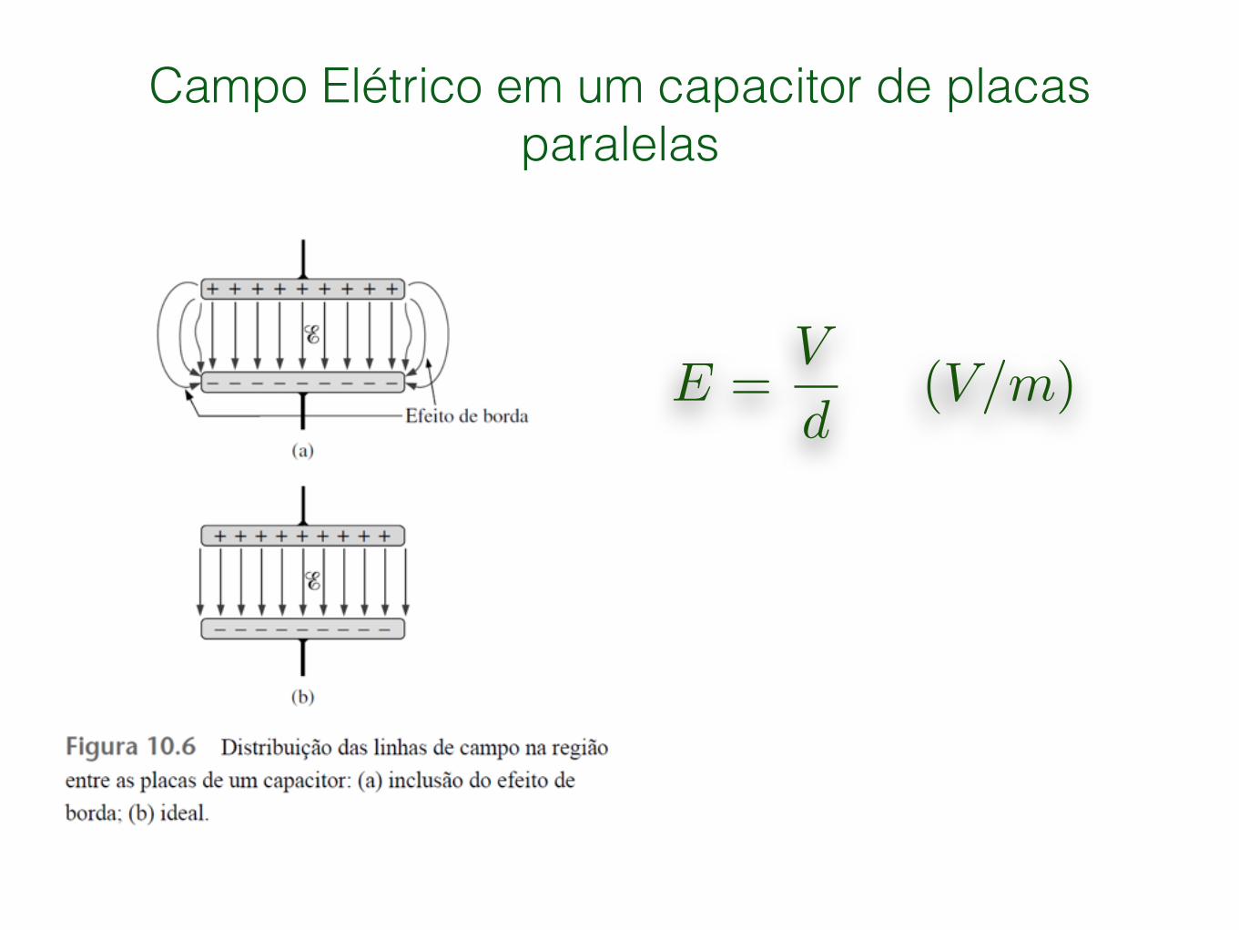
Campo Elétrico em um capacitor de placas paralelas
E =V
d(V/m)
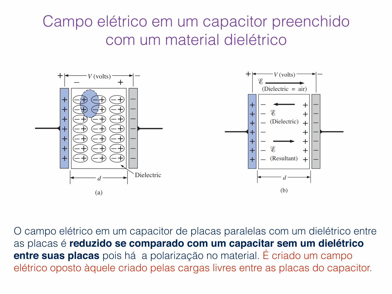
Campo elétrico em um capacitor preenchido com um material dielétrico
O campo elétrico em um capacitor de placas paralelas com um dielétrico entre as placas é reduzido se comparado com um capacitar sem um dielétrico entre suas placas pois há a polarização no material. É criado um campo elétrico oposto àquele criado pelas cargas livres entre as placas do capacitor.
unit area (D) between the two plates is quite uniform. At the edges, theflux lines extend outside the common surface area of the plates, pro-ducing an effect known as fringing. This effect, which reduces thecapacitance somewhat, can be neglected for most practical applications.For the analysis to follow, we will assume that all the flux lines leavingthe positive plate will pass directly to the negative plate within the com-mon surface area of the plates [Fig. 10.5(b)].
If a potential difference of V volts is applied across the two platesseparated by a distance of d, the electric field strength between theplates is determined by
(volts/meter, V/m) (10.6)
The uniformity of the flux distribution in Fig. 10.5(b) also indicatesthat the electric field strength is the same at any point between the twoplates.
Many values of capacitance can be obtained for the same set of par-allel plates by the addition of certain insulating materials between theplates. In Fig. 10.6(a), an insulating material has been placed between aset of parallel plates having a potential difference of V volts acrossthem.
Since the material is an insulator, the electrons within the insulatorare unable to leave the parent atom and travel to the positive plate. Thepositive components (protons) and negative components (electrons) ofeach atom do shift, however [as shown in Fig. 10.6(a)], to form dipoles.
When the dipoles align themselves as shown in Fig. 10.6(a), the mate-rial is polarized. A close examination within this polarized material willindicate that the positive and negative components of adjoining dipolesare neutralizing the effects of each other [note the dashed area in Fig.10.6(a)]. The layer of positive charge on one surface and the negativecharge on the other are not neutralized, however, resulting in the estab-lishment of an electric field within the insulator [!dielectric; Fig. 10.6(b)].The net electric field between the plates (!resultant ! !air " !dielectric)would therefore be reduced due to the insertion of the dielectric.
The purpose of the dielectric, therefore, is to create an electric fieldto oppose the electric field set up by free charges on the parallel plates.For this reason, the insulating material is referred to as a dielectric, difor “opposing” and electric for “electric field.”
In either case—with or without the dielectric—if the potential acrossthe plates is kept constant and the distance between the plates is fixed,the net electric field within the plates must remain the same, as deter-mined by the equation ! ! V/d. We just ascertained, however, that thenet electric field between the plates would decrease with insertion of thedielectric for a fixed amount of free charge on the plates. To compensateand keep the net electric field equal to the value determined by V and d,more charge must be deposited on the plates. [Look ahead to Eq.(10.11).] This additional charge for the same potential across the platesincreases the capacitance, as determined by the following equation:
C D !
For different dielectric materials between the same two parallelplates, different amounts of charge will be deposited on the plates. But
QD#V
! ! #Vd
#
378 C APACITO RS
(a)
!
(b)
++
++
++
+ ––
––
–––
+–
+–
+–
+–
+–
+–
+–
+–
+–
+–
+–
+–
+–
+–
+–
+–
+–
+–
+–
+–
+–
++
++
++
+ ––
––
–––
+– V (volts)+ –
Dielectricd
V (volts)+ –(Dielectric = air)
++
++
++
+––
––
–––
!
!
(Dielectric)
(Resultant)
d
FIG. 10.6Effect of a dielectric on the field distribution
between the plates of a capacitor: (a) alignment of dipoles in the dielectric; (b) electric field components between the
plates of a capacitor with a dielectric present.
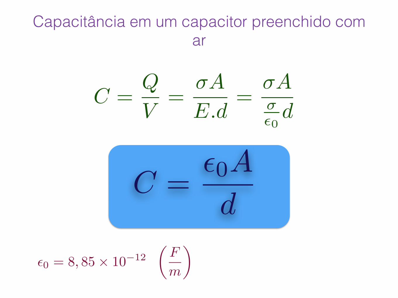
Capacitância em um capacitor preenchido com ar
C =Q
V=
�A
E.d=
�A�✏0d
C =✏0A
d
✏0 = 8, 85⇥ 10�12
✓F
m
◆
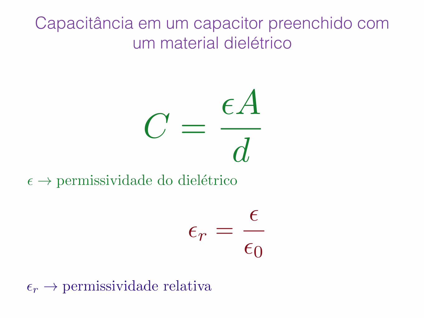
Capacitância em um capacitor preenchido com um material dielétrico
C =✏A
d✏ ! permissividade do dieletrico
✏r =✏
✏0
✏r ! permissividade relativa
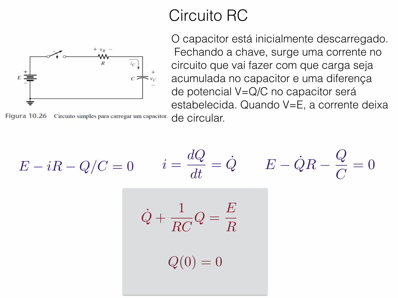
Circuito RC
E � iR�Q/C = 0 i =dQ
dt= Q E � QR� Q
C= 0
Q+1
RCQ =
E
R
Q(0) = 0
O capacitor está inicialmente descarregado. Fechando a chave, surge uma corrente no circuito que vai fazer com que carga seja acumulada no capacitor e uma diferença de potencial V=Q/C no capacitor será estabelecida. Quando V=E, a corrente deixa de circular.
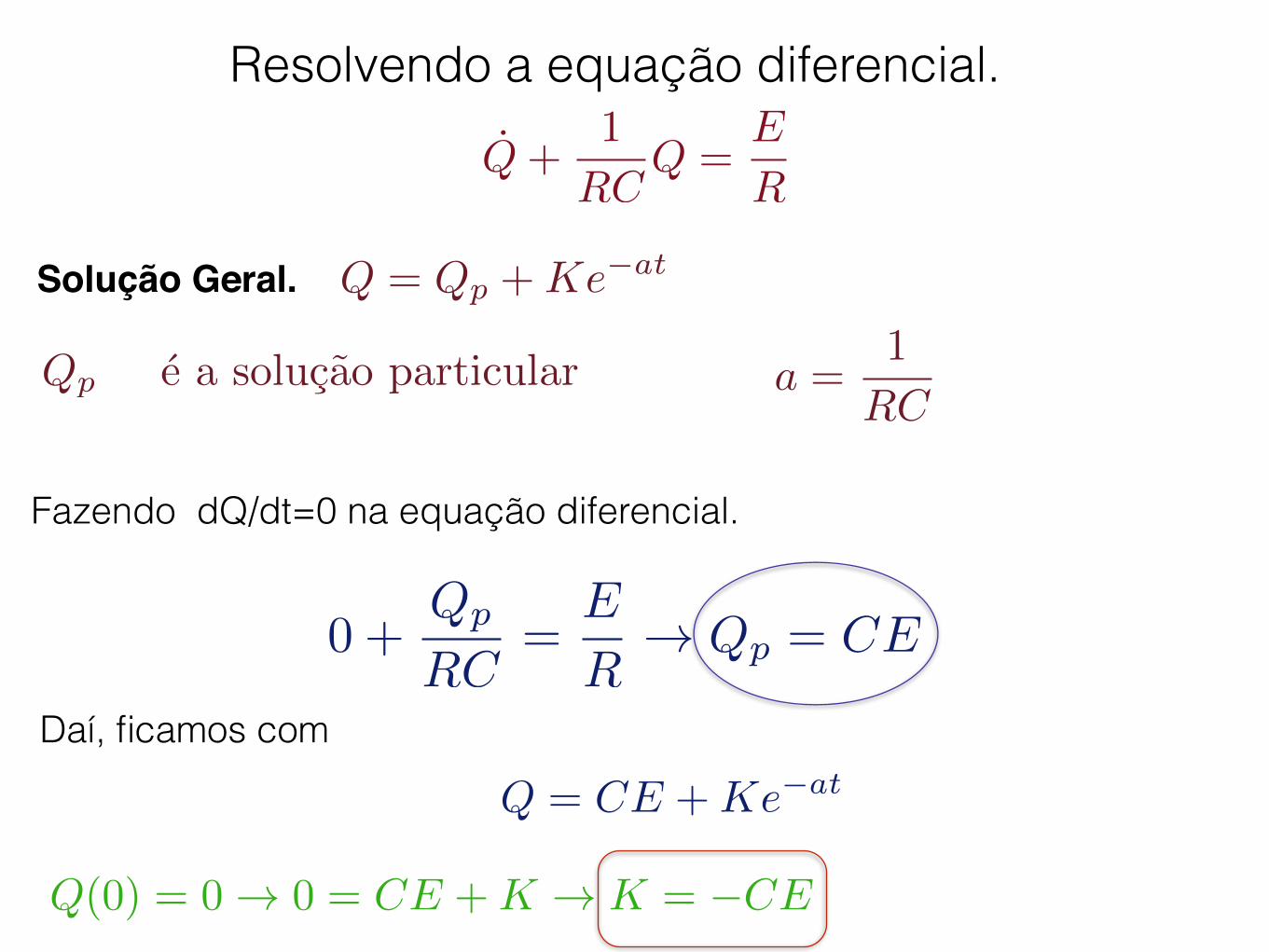
Resolvendo a equação diferencial.
Solução Geral. Q = Qp +Ke�at
Qp e a solucao particular a =1
RC
Fazendo dQ/dt=0 na equação diferencial.
Q+1
RCQ =
E
R
Q = CE +Ke�at
Daí, ficamos com
Q(0) = 0 ! 0 = CE +K ! K = �CE
0 +Qp
RC=
E
R! Qp = CE
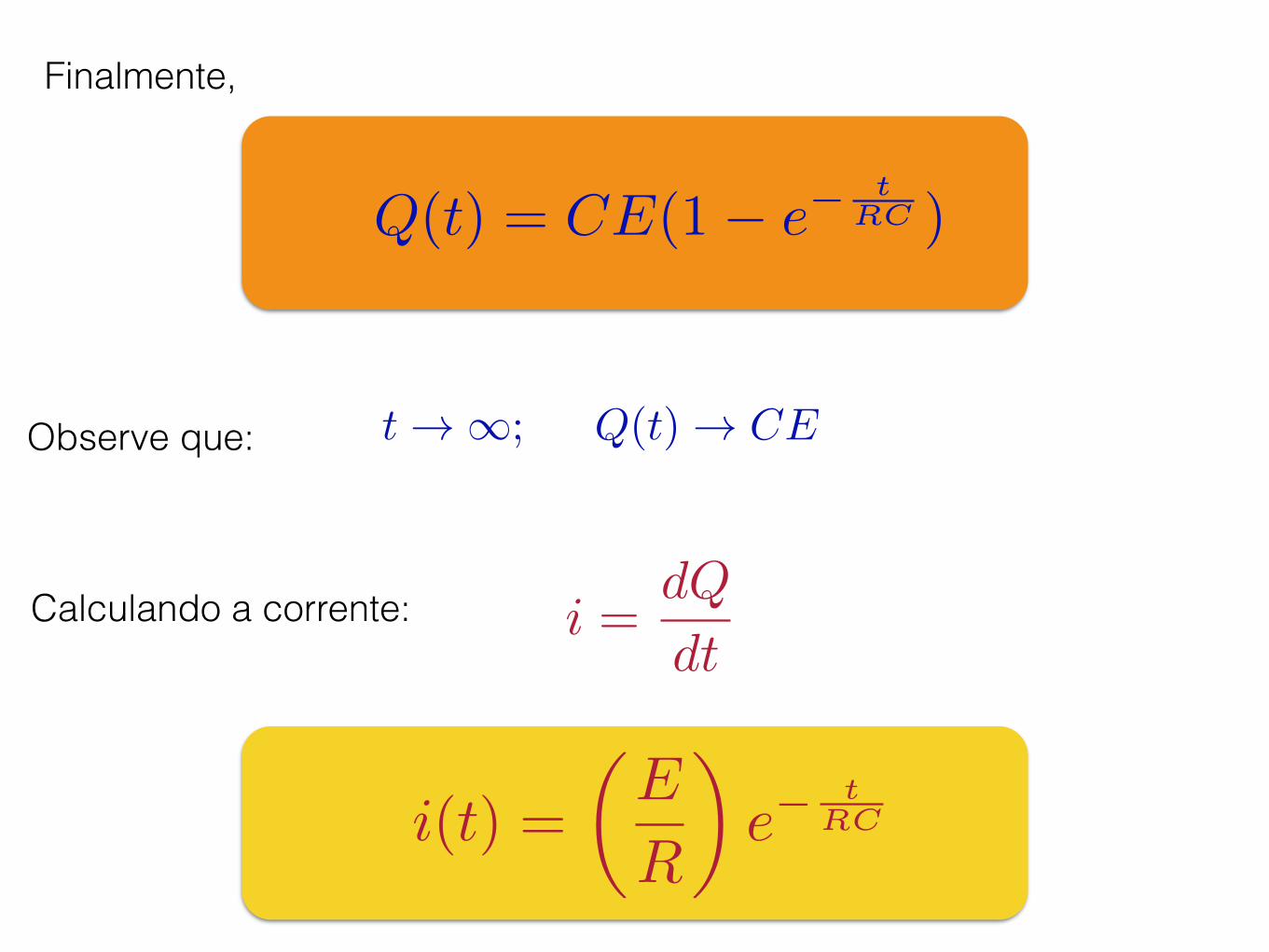
Finalmente,
Q(t) = CE(1� e�t
RC )
Observe que: t ! 1; Q(t) ! CE
Calculando a corrente: i =dQ
dt
i(t) =
✓E
R
◆e�
tRC
392 CAPACITORS
Returning to Eq. (10.13), we find that the multiplying factor E/R isthe maximum value that the current iC can attain, as shown in Fig.10.25. Substituting t ! 0 s into Eq. (10.13) yields
iC ! e"t/RC ! #ER
#e"0 ! #ER
#
verifying our earlier conclusion.For increasing values of t, the magnitude of e"t/t, and therefore the
value of iC, will decrease, as shown in Fig. 10.31. Since the magnitudeof iC is less than 1% of its maximum after five time constants, we willassume the following for future analysis:
The current iC of a capacitive network is essentially zero after fivetime constants of the charging phase have passed in a dc network.
Since C is usually found in microfarads or picofarads, the time con-stant t ! RC will never be greater than a few seconds unless R is verylarge.
Let us now turn our attention to the charging voltage across thecapacitor. Through further mathematical analysis, the following equa-tion for the voltage across the capacitor can be determined:
(10.15)
Note the presence of the same factor e"t/RC and the function (1 "e"t/RC) appearing in Fig. 10.30. Since e"t/t is a decaying function, thefactor (1 " e"t/t) will grow toward a maximum value of 1 with time, asshown in Fig. 10.30. In addition, since E is the multiplying factor, wecan conclude that, for all practical purposes, the voltage vC is E volts
vC ! E(1 " e"t/RC)
E#R
36.8%
13.5%5% 1.8%
0 1 2 3 4 5 t
iC =
0.67%
ER e–t/
ER
iC
! ! ! ! !
!
FIG. 10.31iC versus t during the charging phase.
0 1! 2! 3! 4! 5! 6!
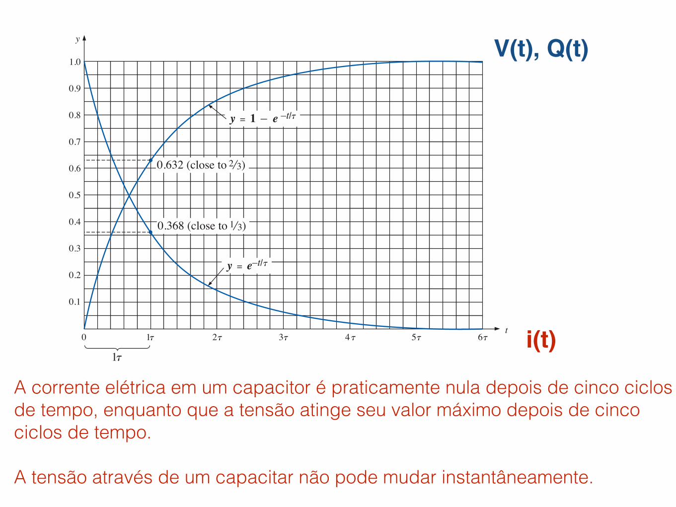
1.0
y
0.9
0.8
0.7
0.6
0.5
0.4
0.3
0.2
0.1
1!
y = e–t/!
y = 1 – e –t/!
0.368 (close to )1 3
0.632 (close to )2 3
t
!
! ! ! ! ! !
!
!
FIG. 10.30Universal time constant chart.
V(t), Q(t)
i(t)
A corrente elétrica em um capacitor é praticamente nula depois de cinco ciclos de tempo, enquanto que a tensão atinge seu valor máximo depois de cinco ciclos de tempo.
A tensão através de um capacitar não pode mudar instantâneamente.
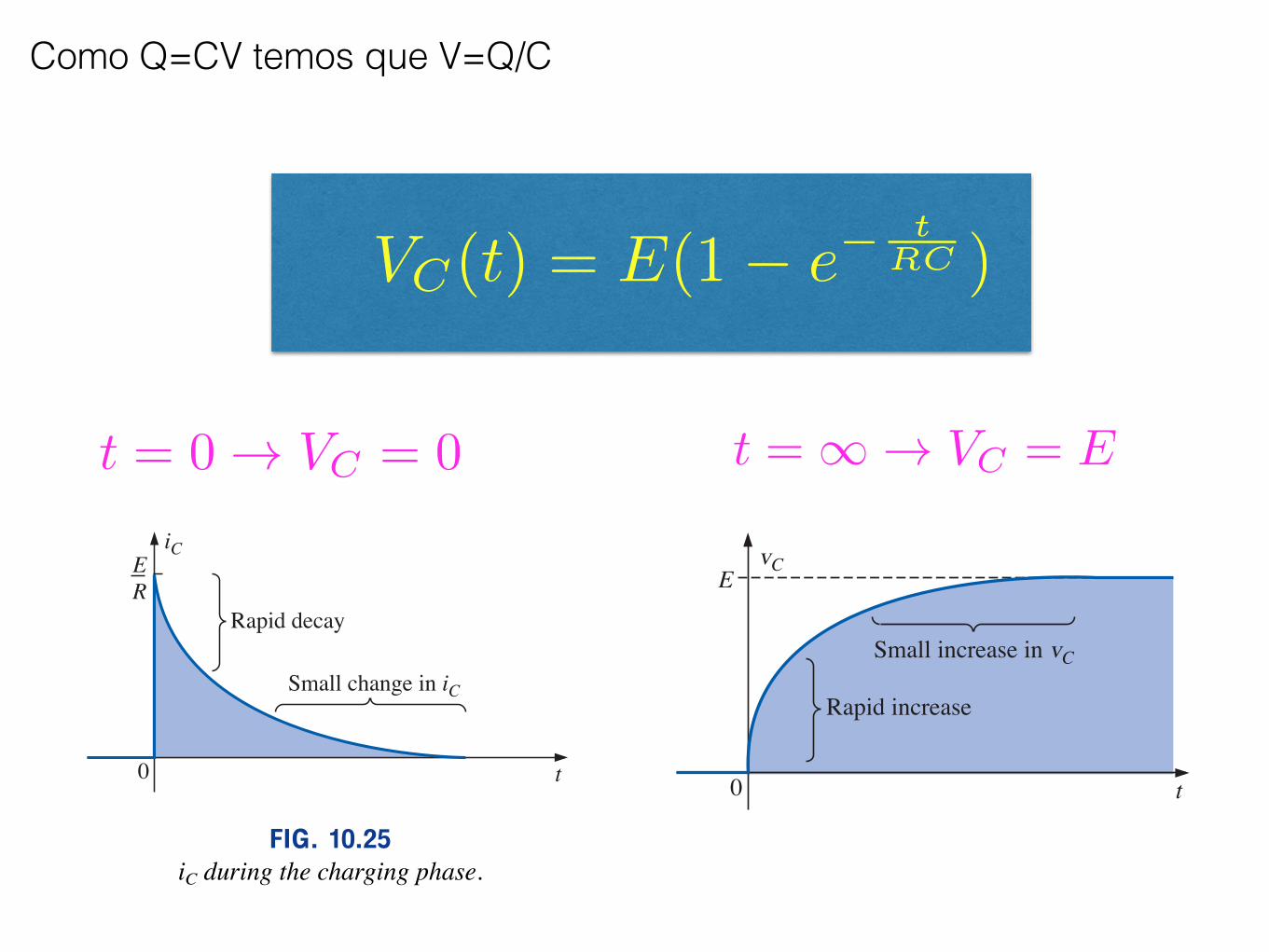
Como Q=CV temos que V=Q/C
VC(t) = E(1� e�t
RC )
t = 1 ! VC = Et = 0 ! VC = 0
390 CAPACITORS
gest the multiplier level. The J represents a !5% tolerance level. Forcapacitors such as appearing in Fig. 10.23(c), the first two numbers areactual digits of the value, while the third number is the power of a mul-tiplier (or number of zeros to be added). The F represents a !1% toler-ance level. Multipliers of 0.01 use an 8, while 9 is used for 0.1 as shownfor the capacitor of Fig. 10.23(d) where the M represents a !20% tol-erance level.
10.7 TRANSIENTS IN CAPACITIVE NETWORKS:CHARGING PHASESection 10.3 described how a capacitor acquires its charge. Let us nowextend this discussion to include the potentials and current developedwithin the network of Fig. 10.24 following the closing of the switch (toposition 1).
You will recall that the instant the switch is closed, electrons aredrawn from the top plate and deposited on the bottom plate by the bat-tery, resulting in a net positive charge on the top plate and a negativecharge on the bottom plate. The transfer of electrons is very rapid atfirst, slowing down as the potential across the capacitor approaches theapplied voltage of the battery. When the voltage across the capacitorequals the battery voltage, the transfer of electrons will cease and theplates will have a net charge determined by Q " CVC " CE.
Plots of the changing current and voltage appear in Figs. 10.25 and10.26, respectively. When the switch is closed at t " 0 s, the currentjumps to a value limited only by the resistance of the network and thendecays to zero as the plates are charged. Note the rapid decay in currentlevel, revealing that the amount of charge deposited on the plates perunit time is rapidly decaying also. Since the voltage across the plates isdirectly related to the charge on the plates by vC " q/C, the rapid ratewith which charge is initially deposited on the plates will result in arapid increase in vC. Obviously, as the rate of flow of charge (I)decreases, the rate of change in voltage will follow suit. Eventually, theflow of charge will stop, the current I will be zero, and the voltage willcease to change in magnitude—the charging phase has passed. At thispoint the capacitor takes on the characteristics of an open circuit: a volt-age drop across the plates without a flow of charge “between” theplates. As demonstrated in Fig. 10.27, the voltage across the capacitoris the source voltage since i " iC " iR " 0 A and vR " iRR " (0)R "0 V. For all future analysis:
A capacitor can be replaced by an open-circuit equivalent once thecharging phase in a dc network has passed.
Looking back at the instant the switch is closed, we can also surmisethat a capacitor behaves as a short circuit the moment the switch isclosed in a dc charging network, as shown in Fig. 10.28. The currenti " iC " iR " E/R, and the voltage vC " E # vR " E # iRR "E # (E/R)R " E # E " 0 V at t " 0 s.
Through the use of calculus, the following mathematical equationfor the charging current iC can be obtained:
(10.13)iC " $ER
$e#t/RC
R
+E
–
+ –vR = 0 V
VC = E
+
–
iC = 0 A
FIG. 10.27Open-circuit equivalent for a capacitor
following the charging phase.
R
+E
–
+ –vR = E
vC = 0 V
+
–
iC = iR = ER
FIG. 10.28Short-circuit equivalent for a capacitor
(switch closed, t " 0).
FIG. 10.24Basic charging network.
+ vR –
2R
+
–vC
1
iC
C
e
E+
–
Rapid decay
Small change in iC
RE
iC
0 t
FIG. 10.25iC during the charging phase.
Small increase in vC
EvC
0 t
Rapid increase
FIG. 10.26vC during the charging phase.
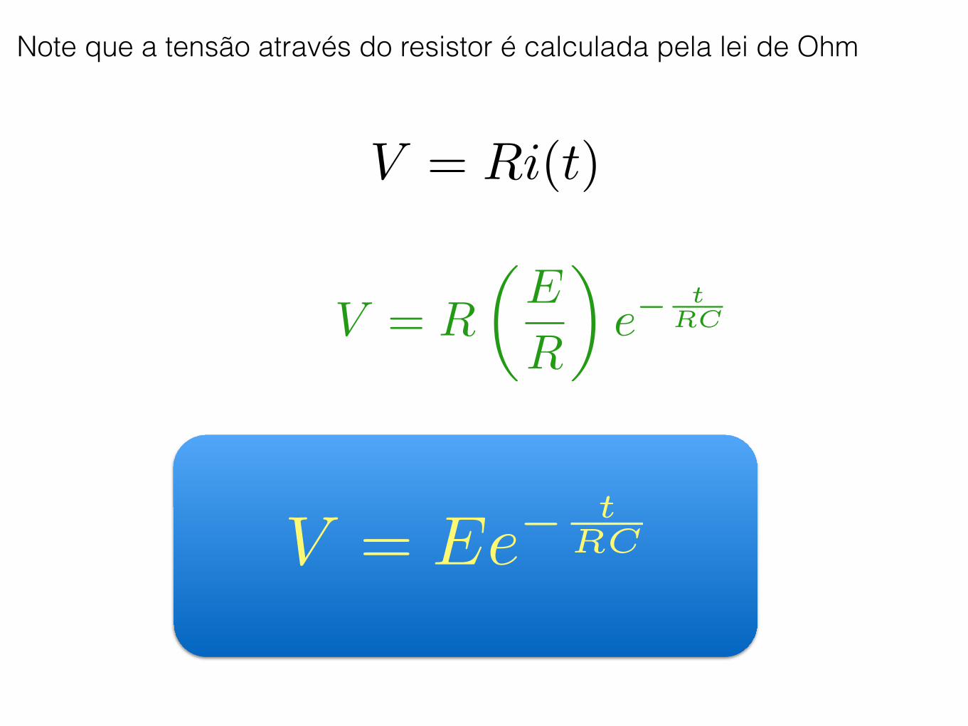
Note que a tensão através do resistor é calculada pela lei de Ohm
V = Ri(t)
V = R
✓E
R
◆e�
tRC
V = Ee�t
RC

Descarga do Capacitor
• Abrindo-se novamente a chave do circuito quando o capacitor está totalmente carregado (Vc=E), ele começa a descarregar-se.
• Como variam a carga, a corrente e a tensão em função do tempo nesta etapa?
• Com a chave aberta a fonte não fornece tensão ao circuito, portanto E=0
• Utilizando Kirchhoff, obtemos a equação diferencial.
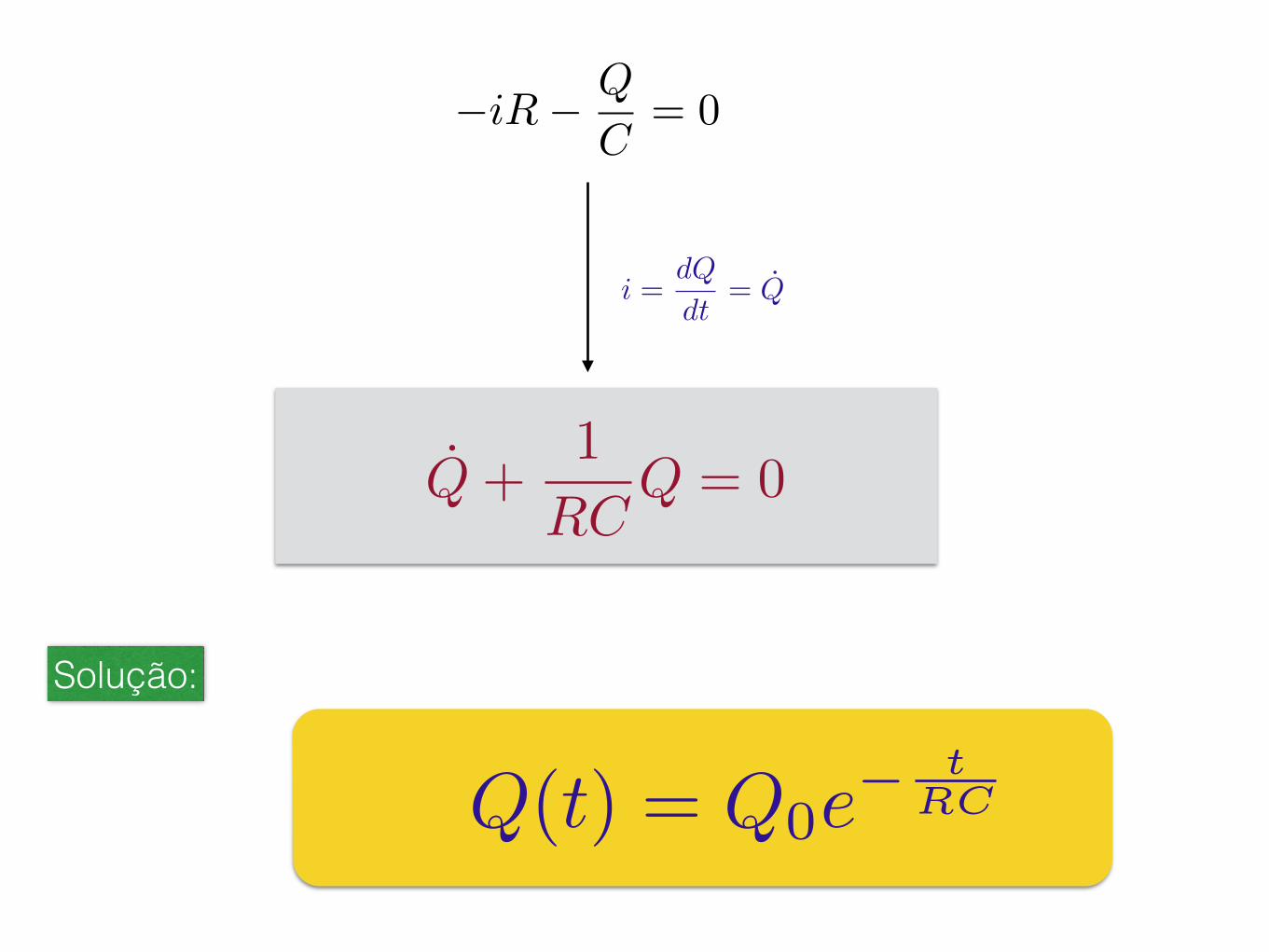
�iR� Q
C= 0
i =dQ
dt= Q
Q+1
RCQ = 0
Solução:
Q(t) = Q0e� t
RC

Quando t=RC
Q(t) = 0, 37Q0
Calculando a corrente i(t) e a tensão V(t), respectivamente.
com
O sinal de (-) somente indica que a partir do desligamento da chave a corrente no capacitor vai diminuir
i(t) = � Q0
RCe�
tRC
VC(t) =Q0
Ce�
tRC com V0 =
Q0
C
i0 =Q0
RC=
E
R
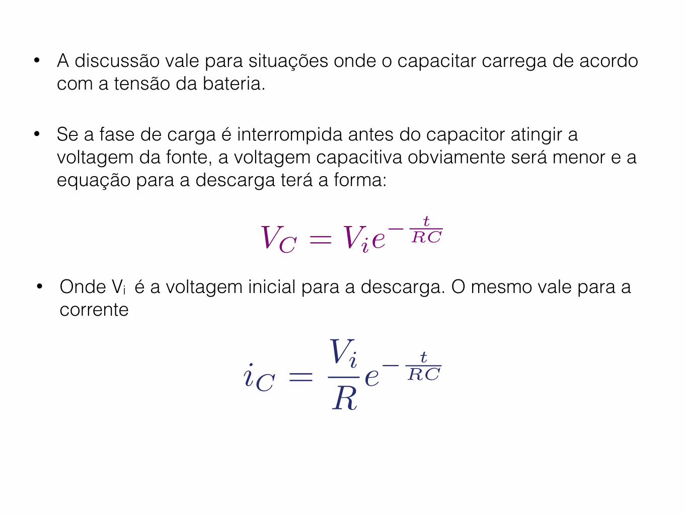
• A discussão vale para situações onde o capacitar carrega de acordo com a tensão da bateria.
• Se a fase de carga é interrompida antes do capacitor atingir a voltagem da fonte, a voltagem capacitiva obviamente será menor e a equação para a descarga terá a forma:
VC = Vie� t
RC
• Onde Vi é a voltagem inicial para a descarga. O mesmo vale para a corrente
iC =Vi
Re�
tRC
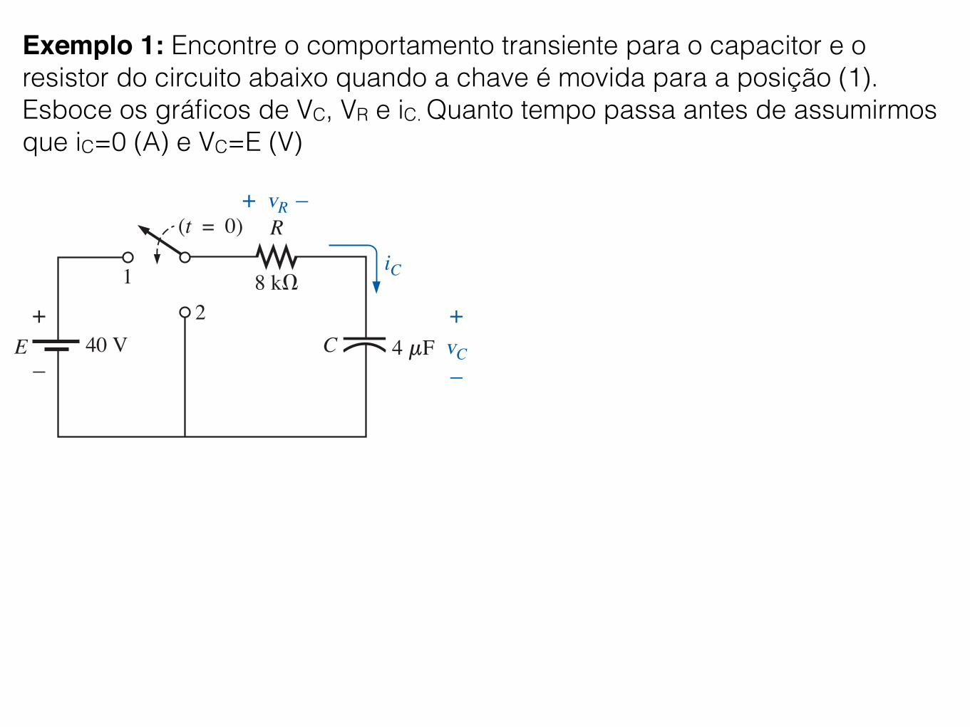
Exemplo 1: Encontre o comportamento transiente para o capacitor e o resistor do circuito abaixo quando a chave é movida para a posição (1). Esboce os gráficos de VC, VR e iC. Quanto tempo passa antes de assumirmos que iC=0 (A) e VC=E (V)
TRANSIENTS IN CAPACITIVE NETWORKS: CHARGING PHASE 393
after five time constants of the charging phase. A plot of vC versus t isprovided in Fig. 10.32.
If we keep R constant and reduce C, the product RC will decrease,and the rise time of five time constants will decrease. The change intransient behavior of the voltage vC is plotted in Fig. 10.33 for variousvalues of C. The product RC will always have some numerical value,even though it may be very small in some cases. For this reason:
The voltage across a capacitor cannot change instantaneously.
In fact, the capacitance of a network is also a measure of how much itwill oppose a change in voltage across the network. The larger thecapacitance, the larger the time constant, and the longer it takes tocharge up to its final value (curve of C3 in Fig. 10.33). A lesser capaci-tance would permit the voltage to build up more quickly since the timeconstant is less (curve of C1 in Fig. 10.33).
The rate at which charge is deposited on the plates during the charg-ing phase can be found by substituting the following for vC in Eq.(10.15):
vC !
and charging (10.16)
indicating that the charging rate is very high during the first few timeconstants and less than 1% after five time constants.
The voltage across the resistor is determined by Ohm’s law:
vR ! iRR ! RiC ! R"ER
"e#t/t
or (10.17)
A plot of vR appears in Fig. 10.34.Applying Kirchhoff’s voltage law to the circuit of Fig. 10.24 will
result in
vC ! E # vR
Substituting Eq. (10.17):
vC ! E # Ee#t/t
Factoring gives vC ! E(1 # e#t/t), as obtained earlier.
EXAMPLE 10.5a. Find the mathematical expressions for the transient behavior of vC,
iC, and vR for the circuit of Fig. 10.35 when the switch is moved toposition 1. Plot the curves of vC, iC, and vR.
b. How much time must pass before it can be assumed, for all practicalpurposes, that iC ! 0 A and vC ! E volts?
Solutions:a. t ! RC ! (8 $ 103 %)(4 $ 10#6 F) ! 32 $ 10#3 s ! 32 ms
By Eq. (10.15),
vC ! E(1 # e#t/t) ! 40(1 ! e!t/(32"10!3))
vR ! Ee#t/t
q ! CvC ! CE(1 # e#t/t)
q"C
vC = E(1 – e–t/
EvC
0 t1 2 3 4 5
63.2%
86.5%95% 98.2% 99.3%
! ! ! ! !
!)
FIG. 10.32vC versus t during the charging phase.
FIG. 10.33Effect of C on the charging phase.
EvC
0 t
C1 C2
C3
C3 > C2 > C1,R fixed
vR = Ee–t/t
EvR
0 t1t 2t 3t 4t 5t
36.8%
13.5%5% 1.8% 0.67%
FIG. 10.34vR versus t during the charging phase.
R
8 k"
C 4 mF vC
+
–
+ vR –(t = 0)
12
E+
–40 V
iC
FIG. 10.35Example 10.5.
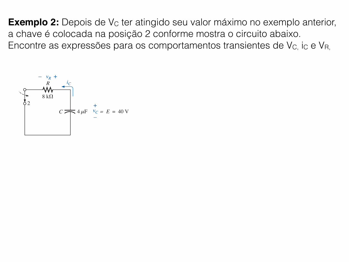
Exemplo 2: Depois de VC ter atingido seu valor máximo no exemplo anterior, a chave é colocada na posição 2 conforme mostra o circuito abaixo. Encontre as expressões para os comportamentos transientes de VC, iC e VR,
DISCHARGE PHASE 395
which employs the function e!x and the same time constant used above.The resulting curve will have the same shape as the curve for iC and vRin the last section. During the discharge phase, the current iC will alsodecrease with time, as defined by the following equation:
discharging(10.19)
The voltage vR " vC, and
discharging (10.20)
The complete discharge will occur, for all practical purposes, in fivetime constants. If the switch is moved between terminals 1 and 2 everyfive time constants, the wave shapes of Fig. 10.39 will result for vC, iC,and vR. For each curve, the current direction and voltage polarities weredefined by Fig. 10.24. Since the polarity of vC is the same for both thecharging and the discharging phases, the entire curve lies above theaxis. The current iC reverses direction during the charging and dis-charging phases, producing a negative pulse for both the current and thevoltage vR. Note that the voltage vC never changes magnitude instanta-neously but that the current iC has the ability to change instantaneously,as demonstrated by its vertical rises and drops to maximum values.
vR " Ee!t/RC
iC " #ER
#e!t/RC
EvC
0 tPos. 1 15tPos. 2 Pos. 1 Pos. 2
E iC
0 tPos. 1
Pos. 2
Pos. 1
Pos. 2
R
EvR
0 tPos. 1
Pos. 2
Pos. 1
Pos. 2
ER
10t5t
Charging Discharging
5t 15t
5t 15t
– E
–
10t
10t
FIG. 10.39The charging and discharging cycles for the
network of Fig. 10.24.8 k!
2
– vR +
+
– vC
R
= E = 40 V
iC
C 4 F"
FIG. 10.40Example 10.6.
EXAMPLE 10.6 After vC in Example 10.5 has reached its final valueof 40 V, the switch is thrown into position 2, as shown in Fig. 10.40.Find the mathematical expressions for the transient behavior of vC, iC,
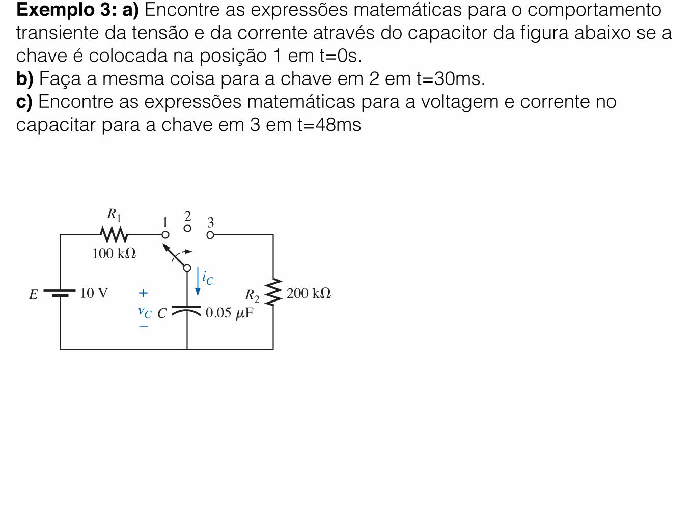
Exemplo 3: a) Encontre as expressões matemáticas para o comportamento transiente da tensão e da corrente através do capacitor da figura abaixo se a chave é colocada na posição 1 em t=0s. b) Faça a mesma coisa para a chave em 2 em t=30ms. c) Encontre as expressões matemáticas para a voltagem e corrente no capacitar para a chave em 3 em t=48ms
396 CAPACITORS
and vR after the closing of the switch. Plot the curves for vC, iC, and vRusing the defined directions and polarities of Fig. 10.35. Assume thatt ! 0 when the switch is moved to position 2.
Solution:
t ! 32 ms
By Eq. (10.18),
vC ! Ee"t/t ! 40e!t/(32"10!3)
By Eq. (10.19),
iC ! "#ER
#e"t/t ! !(5 " 10!3)e!t/(32"10!3)
By Eq. (10.20),
vR ! "Ee"t/t ! !40e!t/(32"10!3)
The curves appear in Fig. 10.41.
The preceding discussion and examples apply to situations in whichthe capacitor charges to the battery voltage. If the charging phase is dis-rupted before reaching the supply voltage, the capacitive voltage will beless, and the equation for the discharging voltage vC will take on theform
(10.21)
where Vi is the starting or initial voltage for the discharge phase. Theequation for the decaying current is also modified by simply substitut-ing Vi for E; that is,
(10.22)
Use of the above equations will be demonstrated in Examples 10.7 and10.8.
EXAMPLE 10.7a. Find the mathematical expression for the transient behavior of the
voltage across the capacitor of Fig. 10.42 if the switch is thrown intoposition 1 at t ! 0 s.
b. Repeat part (a) for iC.c. Find the mathematical expressions for the response of vC and iC if
the switch is thrown into position 2 at 30 ms (assuming that theleakage resistance of the capacitor is infinite ohms).
d. Find the mathematical expressions for the voltage vC and current iCif the switch is thrown into position 3 at t ! 48 ms.
e. Plot the waveforms obtained in parts (a) through (d) on the sametime axis for the voltage vC and the current iC using the definedpolarity and current direction of Fig. 10.42.
iC ! #VR
i#e"t/t ! Iie"t/t
vC ! Vie"t/RC
R2 200 k!
R1
100 k!
E 10 VC 0.05 mF
21 3
iC
vC
+
–
FIG. 10.42Example 10.7.
40vC (V)
0 t1t 2t 3t 4t 5t
t = 32 ms
40
vR (V)
t1t 4t 5t
0iC (mA)
5.0
t = 32 ms
t1t 4t 5t
0
t = 32 ms
2t 3t
2t 3t
FIG. 10.41The waveforms for the network of Fig. 10.40.


![5. Capacitância (baseado no Halliday, 4a edição)hpc.ct.utfpr.edu.br/~rincoski/alunos/Engenharia/FisicaIII/Cap05.pdf · [Cristóvão R M Rincoski] p. 006 5. Capacitância Capítulo](https://img.dokumen.tips/doc/110x75/5be6f00209d3f23a558b5730/5-capacitancia-baseado-no-halliday-4a-edicaohpcctutfpredubrrincoskialunosengenhariafisicaiiicap05pdf.jpg)


![Curso: Ciências da computação Disciplina: Física aplicada ... · Equação 01 – Equação da capacitância de um capacitor de placas planas paralelas [2] Na equação acima](https://img.dokumen.tips/doc/110x75/5b537ed37f8b9a0d398bda85/curso-ciencias-da-computacao-disciplina-fisica-aplicada-equacao.jpg)