Embed Size (px)
Citation preview

PIONEER CORPORATION 4-1, Meguro 1-chomePIONEER ELECTRONICS (USA) INC. P.O. Box 1760, LoPIONEER EUROPE NV Haven 1087, Keetberglaan 1, 912PIONEER ELECTRONICS ASIACENTRE PTE. LTD. 253
PIONEER CORPORATION 2009
DEH-4250SD/XNES
, Meguro-ku, Tokyo 153-8654, Japanng Beach, CA 90801-1760, U.S.A.0 Melsele, Belgium Alexandra Road, #04-01, Singapore 159936
ORDER NO.
CRT4505
CD RECEIVER
DEH-4250SD/XNES
DEH-4250SD/XNES1
DEH-4290SD/XNID
DEH-3200UB/XNUC
This service manual should be used together with the following manual(s):
Model No. Order No. Mech. Module Remarks
CX-3269 CRT4488 S11STD-DOUT CD Mech. Module : Circuit Descriptions, Mech. Descriptions, Disassembly
For details, refer to "Important Check Points for Good Servicing".
K-ZZZ NOV. 2009 Printed in Japan

C
D
F
A
B
E
1 2 3 4
SAFETY INFORMATION
CAUTION
Where in a manufacturer’s service documentation, for example in circuit diagrams or listsof components, a symbol is used to indicate that a specific component shall be replaced onlyby the component specified in that documentation for safety reasons, the following symbol shallbe used:
This service manual is intended for qualified service technicians; it is not meant for the casual do-it-yourselfer.Qualified technicians have the necessary test equipment and tools, and have been trained to properly and safely repaircomplex products such as those covered by this manual.Improperly performed repairs can adversely affect the safety and reliability of the product and may void the warranty.If you are not qualified to perform the repair of this product properly and safely, you should not risk trying to do soand refer the repair to a qualified service technician.
CAUTION:USE OF CONTROLS OR ADJUSTMENTS OR PERFORMANCE OF PROCEDURES OTHER THAN THOSE SPECIFIED HEREIN MAY RESULT IN HAZARDOUS RADIATION EXPOSURE.
- Safety Precautions for those who Service this Unit. When checking or adjusting the emitting power of the laser diode exercise caution in order to get safe, reliable results.
Caution: 1. During repair or tests, minimum distance of 13 cm from the focus lens must be kept.
CAUTIONCLASS 1M INVISIBLE LASER RADIATION WHEN OPEN. DO NOT VIEW DIRECTLY WITH OPTICAL INSTRUMENTS
2. During repair or tests, do not view laser beam for 10 seconds or longer.
WARNING
This product may contain a chemical known to the State of California to cause cancer, or birth defects or other reproductive harm.Health & Safety Code Section 25249.6 - Proposition 65
WARNING!The AEL (accessible emission level )of the laser power output is less than CLASS 1 but the laser component is capable of emitting radiation exceeding the limit for CLASS 1.A specially instructed person should do servicing operation of the apparatus.
Laser diode characteristicsWave length : 785 nm to 814 nm
Maximum output : 1 190 µW(Emitting period : unlimited)
Additional Laser Caution
Transistors Q101 in PCB drive the laser diodes.When Q101 is shorted between their terminals, the laser diodes will radiate beam.If the top cover is removed with no disc loaded while such short-circuit is continued, the naked eyes may be exposed to the laser beam.
DEH-4250SD/XNES21 2 3 4

C
D
F
A
B
E
5 6 7 8
[Important Check Points for Good Servicing]In this manual, procedures that must be performed during repairs are marked with the below symbol.Please be sure to confirm and follow these procedures.
1. Product safety
Please conform to product regulations (such as safety and radiation regulations), and maintain a safe servicing environment by following the safety instructions described in this manual.
1 Use specified parts for repair.
Use genuine parts. Be sure to use important parts for safety.
2 Do not perform modifications without proper instructions.
Please follow the specified safety methods when modification(addition/change of parts) is required due to interferences such as radio/TV interference and foreign noise.
3 Make sure the soldering of repaired locations is properly performed.
When you solder while repairing, please be sure that there are no cold solder and other debris.Soldering should be finished with the proper quantity. (Refer to the example)
4 Make sure the screws are tightly fastened.
Please be sure that all screws are fastened, and that there are no loose screws.
5 Make sure each connectors are correctly inserted.
Please be sure that all connectors are inserted, and that there are no imperfect insertion.
6 Make sure the wiring cables are set to their original state.
Please replace the wiring and cables to the original state after repairs.In addition, be sure that there are no pinched wires, etc.
7 Make sure screws and soldering scraps do not remain inside the product.
Please check that neither solder debris nor screws remain inside the product.
8 There should be no semi-broken wires, scratches, melting, etc. on the coating of the power cord.
Damaged power cords may lead to fire accidents, so please be sure that there are no damages.If you find a damaged power cord, please exchange it with a suitable one.
9 There should be no spark traces or similar marks on the power plug.
When spark traces or similar marks are found on the power supply plug, please check the connection and advise on secure connections and suitable usage. Please exchange the power cord if necessary.
a Safe environment should be secured during servicing.
When you perform repairs, please pay attention to static electricity, furniture, household articles, etc. in order to prevent injuries. Please pay attention to your surroundings and repair safely.
2. Adjustments
To keep the original performance of the products, optimum adjustments and confirmation of characteristics within specification.Adjustments should be performed in accordance with the procedures/instructions described in this manual.
4. Cleaning
For parts that require cleaning, such as optical pickups, tape deck heads, lenses and mirrors used in projection monitors, proper cleaning should be performed to restore their performances.
3. Lubricants, Glues, and Replacement parts
Use grease and adhesives that are equal to the specified substance. Make sure the proper amount is applied.
5. Shipping mode and Shipping screws
To protect products from damages or failures during transit, the shipping mode should be set or the shipping screws should be installed before shipment. Please be sure to follow this method especially if it is specified in this manual.
DEH-4250SD/XNES 35 6 7 8

C
D
F
A
B
E
1 2 3 4
CONTENTS SAFETY INFORMATION..................................................................................................................................... 21. SERVICE PRECAUTIONS ............................................................................................................................... 5
1.1 SERVICE PRECAUTIONS......................................................................................................................... 51.2 NOTES ON SOLDERING .......................................................................................................................... 6
2. SPECIFICATIONS ............................................................................................................................................ 72.1 SPECIFICATIONS...................................................................................................................................... 72.2 DISC/CONTENT FORMAT ........................................................................................................................ 92.3 PANEL FACILITIES.................................................................................................................................. 102.4 CONNECTION DIAGRAM ....................................................................................................................... 12
3. BASIC ITEMS FOR SERVICE........................................................................................................................ 173.1 CHECK POINTS AFTER SERVICING..................................................................................................... 173.2 PCB LOCATIONS .................................................................................................................................... 183.3 JIGS LIST ................................................................................................................................................ 193.4 CLEANING............................................................................................................................................... 19
4. BLOCK DIAGRAM.......................................................................................................................................... 205. DIAGNOSIS.................................................................................................................................................... 23
5.1 OPERATIONAL FLOWCHART ................................................................................................................ 235.2 ERROR CODE LIST ................................................................................................................................ 245.3 CONNECTOR FUNCTION DESCRIPTION............................................................................................. 25
6. SERVICE MODE ............................................................................................................................................ 266.1 DISPLAY TEST MODE ............................................................................................................................ 266.2 CD TEST MODE...................................................................................................................................... 27
7. DISASSEMBLY............................................................................................................................................... 288. EACH SETTING AND ADJUSTMENT ........................................................................................................... 35
8.1 CD ADJUSTMENT................................................................................................................................... 358.2 CHECKING THE GRATING AFTER CHANGING THE PICKUP UNIT.................................................... 36
9. EXPLODED VIEWS AND PARTS LIST.......................................................................................................... 389.1 PACKING ................................................................................................................................................. 389.2 EXTERIOR(1) .......................................................................................................................................... 409.3 EXTERIOR(2) .......................................................................................................................................... 429.4 CD MECHANISM MODULE..................................................................................................................... 44
10. SCHEMATIC DIAGRAM ............................................................................................................................... 4610.1 TUNER AMP UNIT 1/2 [MAIN] (GUIDE PAGE) ..................................................................................... 4610.2 TUNER AMP UNIT 2/2 [MEDIA Ucom] (GUIDE PAGE) ........................................................................ 5210.3 KEYBOARD UNIT.................................................................................................................................. 5810.4 CD CORE UNIT(S11STD-DOUT).......................................................................................................... 6010.5 SD UNIT................................................................................................................................................. 6210.6 WAVEFORMS........................................................................................................................................ 63
11. PCB CONNECTION DIAGRAM ................................................................................................................... 6611.1 TUNER AMP UNIT................................................................................................................................. 6611.2 KEYBOARD UNIT.................................................................................................................................. 7011.3 CD CORE UNIT(S11STD-DOUT).......................................................................................................... 7211.4 SD UNIT................................................................................................................................................. 74
12. ELECTRICAL PARTS LIST .......................................................................................................................... 75
DEH-4250SD/XNES41 2 3 4

C
D
F
A
B
E
5 6 7 8
1. SERVICE PRECAUTIONS1.1 SERVICE PRECAUTIONS
1. You should conform to the regulations governing the product (safety, radio and noise, and other regulations), and should keep the safety during servicing by following the safety instructions described in this manual.2. Before disassembling the unit, be sure to turn off the power. Unplugging and plugging the connectors during power-on mode may damage the ICs inside the unit.3. To protect the pickup unit from electrostatic discharge during servicing, take an appropriate treatment (shorting-solder) by referring to "the DISASSEMBLY".4. After replacing the pickup unit, be sure to check the grating.5. Be careful in handling ICs. Some ICs such as MOS type are so fragile that they can be damaged by electrostatic induction.6. On CD Core Unit, actual cable colors and silk print are different.
7. When a CD-DA (regular music CD) is played in the CD test mode, its sound quality will be temporarily deteriorated. The CD will then repeat normal, deteriorated, normal… playback. This is due to the difference in the playback modes between the normal operation mode and the CD test mode, and the interval of generating deteriorated mode and the time taken to return to the normal mode depend on the error of each clock. The time taken to turn to the deteriorated mode is at a minimum around 20 seconds while the time to return to the normal mode is maximum 40 seconds approximately. Make sure to check the sound quality in the normal operation mode.
Green Red White Black
8. area and a heat sink becomes hot areas. Be careful not to burn yourself.
DEH-4250SD/XNES 55 6 7 8

C
D
F
A
B
E
1 2 3 4
1.2 NOTES ON SOLDERING
For environmental protection, lead-free solder is used on the printed circuit boards mounted in this unit. Be sure to use lead-free solder and a soldering iron that can meet specifications for use with lead-free solders for repairs accompanied by reworking of soldering.
Compared with conventional eutectic solders, lead-free solders have higher melting points, by approximately 40 C. Therefore, for lead-free soldering, the tip temperature of a soldering iron must be set to around 373 C in general, although the temperature depends on the heat capacity of the PC board on which reworking is required and the weight of the tip of the soldering iron.
Compared with eutectic solders, lead-free solders have higher bond strengths but slower wetting times and higher melting temperatures (hard to melt/easy to harden).
The following lead-free solders are available as service parts: Parts numbers of lead-free solder: GYP1006 1.0 in dia. GYP1007 0.6 in dia. GYP1008 0.3 in dia.
DEH-4250SD/XNES61 2 3 4

C
D
F
A
B
E
5 6 7 8
2. SPECIFICATIONS2.1 SPECIFICATIONS
Continuous power output .. 22 W × 4 (50 Hz to 15 000Hz, 5 % THD, 4 ohmload,both channels driven)
Load impedance ................... 4 ohm to 8 ohm × 44 ohm to 8 ohm × 2 + 2 ohm × 1
Preout maximum output level............................................... 2.2 V
Equalizer (5-Band Graphic Equalizer):Frequency.......................100/315/1.25k/3.15k/8k HzGain .................................. ±6 dB
HPF:Frequency...................... 50/63/80/100/125 HzSlope............................... –12 dB/oct
Subwoofer (mono):Frequency...................... 50/63/80/100/125 HzSlope............................... –18 dB/octGain .................................. +6 dB to –24 dBPhase ..............................Normal/Reverse
Bass boost:Gain ................................. +6 dB to 0 dB
CD playerSystem.....................................Compact disc audio systemUsable discs .......................... Compact discSignal-to-noise ratio.............. 94 dB (1 kHz) (IEC-A net-
work)Number of channels ............ 2 (stereo)MP3 decoding format ..........MPEG-1 & 2 Audio Layer 3WMA decoding format ....... Ver. 7, 7.1, 8, 9, 10, 11 (2ch
audio)(Windows Media Player)
AAC decoding format.......... MPEG-4 AAC (iTunes en-coded only) (.m4a)(Ver. 8.2 and earlier)
WAV signal format ................Linear PCM & MS ADPCM(Non-compressed)
SDCompatible physical format
.............................................. Version 2.00Maximum memory capacity
............................................. 32 GB (for SD and SDHC)File system.............................. FAT12, FAT16, FAT32MP3 decoding format ..........MPEG-1 & 2 Audio Layer 3WMA decoding format ....... Ver. 7, 7.1, 8, 9, 10, 11 (2ch
audio)(Windows Media Player)
AAC decoding format.......... MPEG-4 AAC (iTunes en-coded only) (.m4a)(Ver. 8.2 and earlier)
WAV signal format ................Linear PCM & MS ADPCM(Non-compressed)
FM tunerFrequency range................... 87.5 MHz to 108.0 MHzUsable sensitivity................... 9 dBf(0.8 μV/75 ohm, mono,
S/N: 30 dB)Signal-to-noise ratio............. 72 dB (IEC-A network)
AM tunerFrequency range................... 531 kHz to 1 602 kHz (9 kHz)
530 kHz to 1 640 kHz (10kHz)
Usable sensitivity.................. 25 μV(S/N: 20 dB)Signal-to-noise ratio............. 62 dB (IEC-A network)
Infrared remote controlWavelength............................. 940 nm ± 50 nmOutput ......................................typ; 12 mw/sr per Infrared
LED
Note
Specifications and the design are subject to mod-ifications without notice.
GeneralRated power source..............14.4 V DC
(allowable voltage range:10.8 V to 15.1 V DC)
Grounding system.................Negative typeMaximum current consumption
...............................................10.0 A
Dimensions (W × H × D):DIN
Chassis.................. 178 mm × 50 mm × 162mm
Nose....................... 188 mm × 58 mm × 24 mmD
Chassis.................. 178 mm × 50 mm × 162mm
Nose........................ 170 mm × 46 mm × 24 mmWeight ...................................... 1.3 kg
AudioMaximum power output ...... 50 W × 4
50 W × 2/4 ohm + 70 W × 1/2ohm (for subwoofer)
Backup current ..................... 5.0 mA or less
USBUSB standard specification
.............................................. USB 2.0 full speedMaximum current supply ... 500 mAUSB Class.............................. MSC (Mass Storage Class)File system............................. FAT12, FAT16, FAT32MP3 decoding format ..........MPEG-1 & 2 Audio Layer 3WMA decoding format ....... Ver. 7, 7.1, 8, 9, 10, 11 (2ch
audio)(Windows Media Player)
AAC decoding format...........MPEG-4 AAC (iTunes en-coded only) (.m4a)(Ver. 8.2 and earlier)
WAV signal format ................Linear PCM & MS ADPCM(Non-compressed)
ES, ES1
DEH-4250SD/XNES, DEH-4250SD/XNES1, DEH-4290SD/XNID
DEH-4250SD/XNES 75 6 7 8

C
D
F
A
B
E
1 2 3 4
Signal-to-noise ratio............. 72 dB (IHF-A network)
AM tunerFrequency range................... 530 kHz to 1 710 kHzUsable sensitivity.................. 25 μV(S/N: 20 dB)Signal-to-noise ratio............. 62 dB (IHF-A network)
CEA2006 Specifications
Power output ......................... 14 W RMS × 4 Channels (4ohm and 1 % THD+N)
S/N ratio .................................. 91 dBA (reference: 1 W into4 ohm)
Note
Specifications and the design are subject to mod-ifications without notice.
GeneralPower source..........................14.4 V DC (10.8 V to 15.1 V DC
allowable)Grounding system.................Negative typeMaximum current consumption
...............................................10.0 A
Dimensions (W × H × D):DIN
Chassis.................. 178 mm × 50 mm × 162mm(7 in. × 2 in. × 6-1/2 in.)
Nose....................... 188 mm × 58 mm × 24 mm(7-3/8 in.× 2-1/4 in.× 1 in.)
DChassis.................. 178 mm × 50 mm × 162
mm(7 in.× 2 in.× 6-1/2 in.)
Nose....................... 170 mm × 46 mm × 24 mm(6-3/4 in.× 1-7/8 in.× 1 in.)
Weight ..................................... 1.3 kg(2.9 lbs)
AudioMaximum power output ....... 50 W × 4
50 W × 2/4 ohm + 70 W × 1/2ohm (for subwoofer)
Continuous power output ... 22 W × 4 (50 Hz to 15 000Hz, 5 % THD, 4 ohm load,both channels driven)
Load impedance ................... 4 ohm to 8 ohm × 44 ohm to 8 ohm × 2 + 2 ohm × 1
Preout maximum output level............................................... 2.2 V
Equalizer (5-Band Graphic Equalizer):Frequency.......................100/315/1.25k/3.15k/8k HzGain ................................. ±12 dB
HPF:Frequency...................... 50/63/80/100/125 HzSlope................................–12 dB/oct
Subwoofer (mono):Frequency.......................50/63/80/100/125 HzSlope................................–18 dB/octGain ................................. +6 dB to –24 dBPhase ..............................Normal/Reverse
Bass boost:Gain ................................. +12 dB to 0 dB
CD playerSystem.....................................Compact disc audio systemUsable discs ...........................Compact discSignal-to-noise ratio............. 94 dB (1 kHz) (IHF-A net-
work)Number of channels ............ 2 (stereo)MP3 decoding format ......... MPEG-1 & 2 Audio Layer 3WMA decoding format ....... Ver. 7, 7.1, 8, 9, 10, 11 (2ch
audio)(Windows Media Player)
AAC decoding format.......... MPEG-4 AAC (iTunes en-coded only) (.m4a)(Ver. 8.2 and earlier)
WAV signal format ............... Linear PCM & MS ADPCM(Non-compressed)
USBUSB standard specification
............................................... USB 2.0 full speedMaximum current supply .... 500 mAUSB Class............................... MSC(Mass Storage Class)File system.............................. FAT12, FAT16, FAT32MP3 decoding format ..........MPEG-1 & 2 Audio Layer 3WMA decoding format ....... Ver. 7, 7.1, 8, 9, 10, 11 (2ch
audio)(Windows Media Player)
AAC decoding format.......... MPEG-4 AAC (iTunes en-coded only) (.m4a)(Ver. 8.2 and earlier)
WAV signal format ................Linear PCM & MS ADPCM(Non-compressed)
FM tunerFrequency range................... 87.9 MHz to 107.9 MHzUsable sensitivity.................. 9 dBf (0.8 μV/75 ohm, mono,
S/N: 30 dB)
Backup current ...................... 5.0 mA or less
DEH-3200UB/XNUC
DEH-4250SD/XNES81 2 3 4

C
D
F
A
B
E
5 6 7 8
2.2 DISC/CONTENT FORMAT
DEH-4200SD
DEH-4250SD/XNES 95 6 7 8

C
D
F
A
B
E
1 2 3 4
2.3 PANEL FACILITIES
Head unit111 7222333
444555 666
de c abbbfgh 9
8
i
traPtraP
1 SRC/ OFF a 6 / PAUSE
2 S.Rtrv b 1 to 6
3 (list) c 3 /
4MULTI-CONTROL(M.C.)
d 2 /
5 Disc loading slot e 1/iPod
6 (eject) f / DISP/SCRL .
7 USB port g CLK / DISP OFF
8AUX input jack (3.5mm stereo jack)
h BAND / ESC
9 Detach button i
SD memory card slot
You can see the SDmemory card slot ifyou remove thefront panel.
CAUTIONUse an optional Pioneer USB cable (CD-U51E) toconnect the USB audio player/USB memory tothe USB port. Since the USB audio player/USBmemory is projected forward from the unit, it isdangerous to connect directly.Do not use the unauthorized product.
Remote control
Part Operation
j VOLUMEPress to increase or decrease vo-lume.
k MUTEPress to mute. Press again to un-mute.
l / / /
Press to perform manual seektuning, fast forward, reverse andtrack search controls. Also usedfor controlling functions.
m AUDIO Press to select an audio function.
n DISP/SCRLPress to select different displays.Press and hold to scroll throughthe text information.
o Press to pause or resume.
p FUNCTION
Press to select functions.Press and hold to recall the initialsetting menu when the sourcesare off.
qLIST /ENTER
Press to display the list dependingon the source.While in the operating menu,press to control functions.
Only for ES, ES1, ID .
DEH-4250SD/XNES101 2 3 4
C
D
F
A
B
E
5 6 7 8
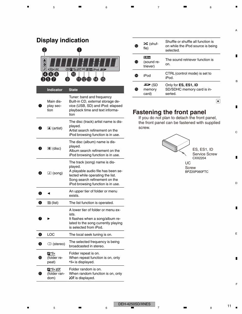
Display indication
12
57 9 bc e f468 a
d3
Indicator State
1Main dis-play sec-tion
Tuner: band and frequencyBuilt-in CD, external storage de-vice (USB, SD) and iPod: elapsedplayback time and text informa-tion
2 (artist)
The disc (track) artist name is dis-played.Artist search refinement on theiPod browsing function is in use.
3 (disc)
The disc (album) name is dis-played.Album search refinement on theiPod browsing function is in use.
4 (song)
The track (song) name is dis-played.A playable audio file has been se-lected while operating the list.Song search refinement on theiPod browsing function is in use.
5An upper tier of folder or menuexists.
6 (list) The list function is operated.
7
A lower tier of folder or menu ex-ists.It flashes when a song/album re-lated to the song currently playingis selected from iPod.
8 LOC The local seek tuning is on.
9 (stereo)The selected frequency is beingbroadcasted in stereo.
a (folder re-peat)
Folder repeat is on.When repeat function is on, only
is displayed.
b (folder ran-dom)
Folder random is on.When random function is on, only
is displayed.
c(shuf-
fle)
Shuffle or shuffle all function ison while the iPod source is beingselected.
d (sound re-triever)
The sound retriever function ison.
e iPodCTRL(control mode) is set toiPod.
f(SD
memorycard)
Only for ES, ES1, IDSD/SDHC memory card is in-serted.
Fastening the front panelIf you do not plan to detach the front panel, the front panel can be fastened with supplied screw.
UCScrewBPZ20P060FTC
ES, ES1, IDService ScrewCXX2204
DEH-4250SD/XNES 115 6 7 8

C
D
F
A
B
E
1 2 3 4
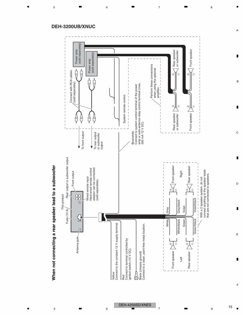
2.4 CONNECTION DIAGRAM
1. T
his
prod
uct
3. F
ront
out
put
5. F
use
(10
A)
2. R
ear
outp
ut o
rsu
bwoo
fer
outp
ut
4.W
ired
rem
ote
inpu
t H
ard-
wire
dre
mot
e co
ntro
lad
apto
r ca
n be
con
nect
ed
(sol
d se
para
tely
).
6. A
nten
na ja
ck
7.Ye
llow
Con
nect
to th
e co
nsta
nt 1
2 V
sup
ply
term
inal
.
8.R
edC
onne
ct to
term
inal
con
trol
led
by
igni
tion
switc
h (1
2 V
DC
).
9.B
lack
(ch
assi
s gr
ound
)C
onne
ct to
a c
lean
, pai
nt-f
ree
met
al lo
catio
n.
th
giR.61
tfeL.51
22.W
ith a
2 s
peak
er s
yste
m, d
o no
t con
nect
anyt
hing
to th
e sp
eake
r le
ads
that
are
not c
onne
cted
to s
peak
ers.
14. F
ront
spe
aker
21. R
ear
spea
ker
10. W
hite
12. G
ray
13. G
ray/
blac
k11
. W
hite
/bla
ck
17. G
reen
19.V
iole
t
18. G
reen
/bla
ck20
.Vio
let/b
lack
14. F
ront
spe
aker
21. R
ear
spea
ker
23.T
ore
ar o
utpu
t or
subw
oofe
r ou
tput
26.P
ower
am
p (s
old
sepa
rate
ly)
25.C
onne
ct w
ith R
CA
cab
les
(sol
d se
para
tely
)
24.T
o fr
ont o
utpu
t
26.P
ower
am
p (s
old
sepa
rate
ly)
29.P
erfo
rm th
ese
conn
ectio
nsw
hen
usin
g th
e op
tiona
lam
plifi
er.
28. S
yste
m r
emot
e co
ntro
l
27.B
lue/
whi
teC
onne
ct to
sys
tem
con
trol
term
inal
of t
hepo
wer
am
p or
aut
o-an
tenn
a re
lay
cont
rol
term
inal
(m
ax. 3
00 m
A 1
2 V
DC
).
rekaepstnorF.41
rekaepstnorF.41 30
. Rea
r sp
eake
ror
sub
woo
fer
30. R
ear
spea
ker
or s
ubw
oofe
r
DEH-4250SD/XNES, DEH-4250SD/XNES1
DEH-4250SD/XNES121 2 3 4

C
D
F
A
B
E
5 6 7 8
)
31.N
ote
Cha
nge
the
initi
al s
ettin
g of
this
uni
t. T
he s
ubw
oofe
r ou
tput
of t
his
unit
is m
onau
ral.
7.Ye
llow
Con
nect
to th
e co
nsta
nt 1
2 V
sup
ply
term
inal
.
8.R
edC
onne
ct to
term
inal
con
trol
led
by
igni
tion
switc
h (1
2 V
DC
).
9.B
lack
(ch
assi
s gr
ound
)C
onne
ct to
a c
lean
, pai
nt-f
ree
met
al lo
catio
n.
1. T
his
prod
uct
3. F
ront
out
put
5. F
use
(10
A)
2. R
ear
outp
ut o
rsu
bwoo
fer
outp
ut
4.W
ired
rem
ote
inpu
t H
ard-
wire
dre
mot
e co
ntro
lad
apto
r ca
n be
con
nect
ed(s
old
sepa
rate
ly).
6. A
nten
na ja
ck
32. S
ubw
oofe
r (4
)
33.W
hen
usin
g a
subw
oofe
r of
70
W (
2 ),
be
sure
to c
onne
ctw
ithV
iole
t and
Vio
let/b
lack
lead
s of
this
uni
t. D
o no
t con
nect
any
thin
g w
ith G
reen
and
Gre
en/b
lack
lead
s.
35.S
ubw
oofe
r(4
) 2
34. N
ot u
sed.
15.L
eft
16. R
ight
14. F
ront
spe
aker
10. W
hite
12. G
ray
13. G
ray/
blac
k11
. W
hite
/bla
ck
17. G
reen
19.V
iole
t
18. G
reen
/bla
ck20
.Vio
let/b
lack
14. F
ront
spe
aker
27.B
lue/
whi
teC
onne
ct to
sys
tem
con
trol
term
inal
of t
he p
ower
am
p or
au
to-a
nten
nare
lay
cont
rol
term
inal
(m
ax. 3
00 m
A 1
2 V
DC
).
32. S
ubw
oofe
r (4
17. G
reen
19.V
iole
t
18. G
reen
/bla
ck20
.Vio
let/b
lack
DEH-4250SD/XNES 135 6 7 8

C
D
F
A
B
E
1 2 3 4
Connect with RCA cables(sold separately)
Rear output orsubwoofer output
This product
Antenna jack
Fuse (10 A)
Blue/whiteConnect to system control terminal of thepower amp or aut o-antenna relay controlterminal (max. 300 mA 12 V DC).
YellowConnect to the constant 12 Vsupply terminal.
RedConnect to terminal controlled by ignition switch (12 V DC).
Black (chassis ground) Connect to a clean, paint-freemetal location.
System remote control
Left Right
Perform these connections when usingthe optional amplifier.
White/black
Violet/black
Violet
With a 2 speaker system, do not connect anything to the speaker leads that are not connected to speakers.
Front speaker
White
Gray/black
Gray
Green/black
Green
Rear speaker
Wired remote input Hard-wired remote control adaptor can be connected (sold separately).
Front output
Power amp(sold separately)
Power amp(sold separately)
Front speaker
Rear speaker
Front speaker
Rear speaker
Front speaker
Rear speaker
DEH-4290SD/XNID
DEH-4250SD/XNES141 2 3 4
C
D
F
A
B
E
5 6 7 8
Wh
en n
ot
con
nec
tin
g a
rea
r sp
eake
r le
ad t
o a
su
bw
oo
fer
Yello
wC
onne
ct to
the
cons
tant
12
V s
uppl
y te
rmin
al.
Red
Con
nect
to te
rmin
al c
ontr
olle
d by
ig
nitio
n sw
itch
(12
V D
C).
Bla
ck (
chas
sis
grou
nd)
Con
nect
to a
cle
an, p
aint
-fre
e m
etal
loca
tion.
Thi
s pr
oduc
t
Fro
nt o
utpu
t
Rig
htLe
ft
With
a 2
spe
aker
sys
tem
, do
not
conn
ect a
nyth
ing
to th
e sp
eake
r le
ads
that
are
not
con
nect
ed to
spe
aker
s.
Fro
nt s
peak
er
Rea
r sp
eake
r
Whi
teG
ray
Gra
y/bl
ack
Whi
te/b
lack
Gre
enV
iole
t
Gre
en/b
lack
Vio
let/b
lack
Rea
r ou
tput
or
subw
oofe
r ou
tput
Ant
enna
jack
Wire
dre
mot
e in
put
Har
d-w
ired
rem
ote
cont
rol
adap
tor
can
be c
onne
cted
(s
old
sepa
rate
ly).
Fus
e (1
0 A
)
Fro
nt s
peak
er
Rea
r sp
eake
r
Con
nect
with
RC
A c
able
s (s
old
sepa
rate
ly)
Per
form
thes
e co
nnec
tions
w
hen
usin
g th
e op
tiona
l am
plifi
er.
Sys
tem
rem
ote
cont
rol
Blu
e/w
hite
Con
nect
to s
yste
m c
ontr
ol te
rmin
al o
f the
pow
er
amp
or a
uto-
ante
nna
rela
y co
ntro
l ter
min
al (
max
. 30
0 m
A 1
2 V
DC
).
Pow
er a
mp
(sol
d se
para
tely
)
Fro
nt s
peak
er
Pow
er a
mp
(sol
d se
para
tely
)To
rear
out
put
or s
ubw
oofe
r ou
tput
To fr
ont o
utpu
t Fro
nt s
peak
er
Rea
r sp
eake
r or
sub
woo
fer
Rea
r sp
eake
r or
sub
woo
fer
DEH-3200UB/XNUC
DEH-4250SD/XNES 155 6 7 8

C
D
F
A
B
E
1 2 3 4
Wh
en u
sin
g a
su
bw
oo
fer
wit
ho
ut
usi
ng
th
e o
pti
on
al a
mp
lifie
r
Not
eC
hang
e th
e in
itial
set
ting
of th
is u
nit.
The
sub
woo
fer
outp
ut o
f thi
s un
it is
mon
aura
l.
Yello
wC
onne
ct to
the
cons
tant
12
V s
uppl
y te
rmin
al.
Red
Con
nect
to te
rmin
al c
ontr
olle
d by
igni
tion
switc
h (1
2 V
DC
).
Bla
ck (
chas
sis
grou
nd)
Con
nect
to a
cle
an, p
aint
-fre
e m
etal
loca
tion.
Thi
s pr
oduc
t
Fro
nt o
utpu
t
Rea
r ou
tput
or
subw
oofe
r ou
tput
Ant
enna
jack
Wire
dre
mot
e in
put
Har
d-w
ired
rem
ote
cont
rol
adap
tor
can
be c
onne
cted
(s
old
sepa
rate
ly).
Fus
e (1
0 A
)
Left
Rig
ht
Fro
nt s
peak
erF
ront
spe
aker
Whi
teG
ray
Gra
y/bl
ack
Whi
te/b
lack
Gre
enV
iole
t
Gre
en/b
lack
Vio
let/b
lack
Gre
enV
iole
t
Gre
en/b
lack
Vio
let/b
lack
Sub
woo
fer
(4
4(S
ubw
oofe
r)
)
Whe
n us
ing
a su
bwoo
fer
of 7
0 W
(2
), b
e su
re to
con
nect
w
ithV
iole
t and
Vio
let/b
lack
lead
s of
this
uni
t. D
o no
t con
nect
any
thin
g w
ith G
reen
and
Gre
en/b
lack
lead
s.
Sub
woo
fer
(4)
x 2
Not
use
d.
Blu
e/w
hite
Con
nect
to s
yste
m c
ontr
olte
rmin
al o
f the
pow
er a
mp
or
auto
-ant
enna
rela
y co
ntro
lte
rmin
al (
max
. 300
mA
12
V D
C).
DEH-4250SD/XNES161 2 3 4

C
D
F
A
B
E
5 6 7 8
3. BASIC ITEMS FOR SERVICE3.1 CHECK POINTS AFTER SERVICING
To keep the product quality after servicing, please confirm following check points.
demrifnocebotmetIserudecorP.oN1 Confirm whether the customer complain has
been solved.If the customer complain occurs with thespecific media, use it for the operation check.
The customer complain must not bereappeared.Display, audio and operations must benormal.
2 CD Play back a CD.(Track search)
No malfunction on display, audio andoperation.
3 FM/AM tuner Check FM/AM tuner action.(Seek, Preset)Switch band to check both FM and AM.
Display, audio and operations must benormal.
4 Check whether no disc is inside the product. The media used for the operating check mustbe ejected.
retfaecnaraeppastinotridrosehctarcsoNkcehcecnaraeppA5receiving it for service.
See the table below for the items to be checked regarding audio:
Item to be checked regarding audioDistortionNoiseVolume too lowVolume too highVolume fluctuatingSound interrupted
DEH-4250SD/XNES 175 6 7 8

C
D
F
A
B
E
1 2 3 4
3.2 PCB LOCATIONS
A
B Keyboard Unit
D SD Unit
CD Core Unit (S11 STD-DOUT)C
Tuner Amp Unit
(DEH-4250SD/XNES)(DEH-4250SD/XNES1)(DEH-4290SD/XNID)
A:DEH-4250SD/XNES
B:DEH-4250SD/XNES1
C:DEH-4290SD/XNID
D:DEH-3200UB/XNUC
Unit Number : CWN4805(A,B,C)
Unit Number : CWN5219(D)
Unit Name : Tuner Amp Unit
Unit Number : CWN4813(A,B,C)
Unit Name : Keyboard Unit
Unit Number : CWN5220(D)
Unit Name : Keyboard Unit
Unit Number : CWX3774
Unit Name : CD Core Unit(S11STD-DOUT)
Unit Number : CWN4816(A,B,C)
Unit Name : SD Unit
DEH-4250SD/XNES181 2 3 4

C
D
F
A
B
E
5 6 7 8
3.3 JIGS LIST
3.4 CLEANING
- Jigs List NameTest DiscL.P.F.
Jig No.TCD-782
RemarksChecking the gratingChecking the grating (Two pieces)
Name Jig No. Remarks
- Grease List NameGreaseGrease
Grease No.GEM1024GEM1045
RemarksCD Mechanism ModuleCD Mechanism Module
Name Grease No. Remarks
Before shipping out the product, be sure to clean the following portions by using the prescribed cleaning tools:
Portions to be cleaned Cleaning tools
CD pickup lenses Cleaning liquid : GEM1004
Cleaning paper : GED-008
DEH-4250SD/XNES 195 6 7 8

C
D
F
A
B
E
D
_RX
_TX
MUTE
STBY
T
CE1
CE2
CK
DI
DO
TL
LG
L
RST
IC60COMPU
PEG640
YSTEM M
WM876IC18DAC
LRCIN
DIN
BCKIN
DEEMPH
MCLK
Q591
ONT
1 2 3 4
4. BLOCK DIAGRAM
JA401
JA661
ANTENNA
SL
FM/A
M TU
NER
UN
IT
VCC
FMANTAMANT
13
5CE2
6CE1
8CK
9DI
10DO
14
4 SYS8V
TUNER AMP UNITA
ROM_VDD13 VDD3.3
VDD_3.317
Lch TUNL23
SYS8V3 1
NJM2885DL1-33IC431
TUNER3V REG.
USB5V DD5V5 4
R5523N001BIC151
USB5V REG.
VOUT VIN1
EN3
FLG
DD5V BUP2 1
BD9781HFPIC161
DD5V REG.
SW VIN
7EN
VDD3.3
3292
KEYA
34MED
33MED
43MED
41MED
KEYD
63
95SL
10RESE
64TUNP
TUNP
65TUNP
66TUNP
67TUNP
36USBC
23USBF
24
80SDCT
SYNC
12S-80827CNNB-B8M
IC651RESET
VDD3.3
S651
R5S7262ZD144FPUIC501
CN701
MEDIA uCOM
114SD_CD
113CDRST
RESET
16
15
8
9
VDD
63SYS_TXD
61
59
58BRST
MEDIAMUTE
SYS_RXD
71
70DM
DP
WIRED REMOTE
2,3
1
KEYADKEYD
231 GND
VDD3.3 VDD51 5
S-1132B33-U5IC901
VDD3.3V REG.
VOUT VIN4
SW
SD_DATA0 - SD_DATA3, SD_CLK, SD_CMD
CN781
SW33V
SD_CD
4
9
DAT0 - DAT3, CLK, CMD
CN1203 CN1202
VDD
CD
VDD
CD
4
12
7
2
MED3.3V
Q781
Q783Q782
SD UNITD
SD3.3V REG.
CPICKUP UNIT(P10.5)(SERVICE)
CD CORE UNIT(S11STD-DOUT)
LD
MD
LD-
MD
HOLOGRAM UNIT
LD+
FOCUS ACT.TRACKING ACT.
FOP
TOP
VREF
FOM
TOM
VCCVCC
15
5
14
15
5
2
1
2
1
14
88
33
44
1212
RF AMP, CD DECODER, MP3&WMA DECODERDIGITAL SERVO/DATA•PROCESSOR
CPU, USB HOST CONTROLLER
PE5706AIC201
Q101
IC301BA5839FP
ACTUATOR/MOTOR DRIVER
CN101
TD,FD
AC,BD,E,F
1
2
VDD
TOP
FOP
REFO93
FOM
TOM
PD
REFO
V+3A
LD+
GND
SPINDLEMOTOR
LOADING/CARRIAGEMOTOR
21
9
SD,MD
40
39
22 4115 VO3+16 VO3-17 VO4+18 VO4-
11 VO1-14 VO2+
12 VO1+
13 VO2-SOMSOP
LCOMLCOP
CNT
MUTE
LOIN
S903 S901S905DSCSNS HOME8SNS
35
3738
LD
PD
CONT
CLCONT
HOME
8SNSDSCSNS
RESET
REFOUT
LOEJ
PUENCN701
2VD
1
Q102
54
V+3A VDD
CD DATA (CDSRQ,CDSTBY,SKIP,
29 RESET
SCL,SDA,DATA,BCLK,LRCK,WAIT)
9
8
VDD
CD DATA (CDSRQ,CDSTBY,SKIP,SCL,SDA,DATA,BCLK,LRCK,WAIT)
M
M
MED21
CWW1967IC571
FLASH ROM 16Mbit
12RESET
43RESET
S
138DACLRCK
137DACDATA
139
105
136DACCLK
DACDATA1
DACSCK
1
2
3
12
14
148CP_SDA
149CP_SCL
112CPRST
111CPPWR
MED3.3V
A B
:DEH-4250SD/XNES:DEH-4250SD/XNES1
A
:DEH-4290SD/XNID:DEH-3200UB/XNUCC
B
VDVD
85VDSENS
BUP
Q751
Q752
MECHA VD
19 VDC
DEH-4250SD/XNES201 2 3 4

C
D
F
A
B
E
3292
34
33
43
41
63
95
10
64
65
66
67
36
23
24
80
21
MED3.3V
19
5 6 7 8
17 DSENS
DSENS
CN801
SOURCE
SW3.3V
KYDT
DPDT
ROT1ROT0
3
8
11
16
19
4
6
10
1214
D+
D-15
13
VBUSUSB5V
AUXL
OEL+B
SYS8V BUP2 1
NJM2388F84IC911
SYS8V REG.
VOUT VIN
4CONTROL
BUP
PM9012AIC201E.VOL
25OUTFL
26
FL
RLOUTRL
36TUNL
35CDLS5B+L
27 SWLOUTPL
39AUXLS1Q+L
S4B-L
21
22CLK
STB
23DATA
PA2030AIC351AMP
9OUT1(+)
7 FL2OUT1(-)
12RL
11FLIN1
FL
5 RL1OUT2(+)
3 RL2OUT2(-)
25 BRE1H-SW/VDS-DET
IN2
22MUTE
4STBY
48MUTE
46SYSPW
KEYAD
16
18
40TELIN
MED_RX
MED_TX
MEDMUTE
MEDSTBY
KEYD
SL
ASENS
RESET
BSENS
TUNPCE1
TUNPCE2
TUNPCK
TUNPDI
TUNPDO
55VST
54VCK
53VDT
USBCTL
USBFLG
SDCTL
SYNC
JA301
JA981FL1
1
3
5
7
18
14
ACC113
TEL19
6FL
5SWLSWL
Q303
Q301
Q361
Q381
Q382
VDD5
BUP
BUP
Q363
RC
A OU
T
MED3.3V
DD5V1 6
S-1172B33-E6IC581
MED3.3V REG.
VOUT VIN3
ON/OFFMED1.2V
4 3
BH12PB3WHFVIC583
MED1.2V REG.
VOUT VIN1
STBY
MEDRST
IC601COMPUTER
PEG640A8
SYSTEM MICRO
BUP
Q831
Q832
BUP VDD5
Q901
Q902
45DALMON
50OELPW
VDD5V REG.
OEL+B
OEL+B
90 SOURCE
30KYDT
SSENS
29
VDD3.3
Q841
Q842
BUP
Q821
Q822
47SWVDD
49ILMPW
DPDT
1ROT1
2ROT0
ILM+B
SWVDD
ILM+B
51
NJM2872F05IC182
DAC5V REG.
SYS8V
WM8761GEDIC181DAC
9VOUTL
CDL1
LRCIN2
DIN3
BCKIN12
DEEMPH14
MCLK8
VDDVIN
3CONT
VOUT
Q591
341S2162IC591
iPod CP
13I2C_SDA/SPI_SOMI
12I2C_SCL/SPI_SIMO
4nRESET
5VCC
2MODE1/SPI_nSS
Q921
BSENS
ASENS
SOUR
CE
CO
NNE
CTOR
C
TELMUTEQ951
3
16
KEYBOARD UNITBCN1801
JA1801
19 AUXL
4SOURCE
SW3.3V
CN1802
4D+
3D-
2US5V
SW3.3V
6KYDT
10DPDT
ROT014
15D+
13D-
S1801
ILLUMI
13 KYDT12 DPDT
MCLKR-ILM
14
19
XREST 11
XCMD 20
DCLK 1
DOUT 2
ADKEY117
REM 10
ADKEY215
CN1921
10XI
7XCS
6XRES
5XCMD
4SCL
3SI_RX
KEY MATRIX
1 3GP1UXC14RK
IC1891
S1811ROTARY COMMANDER
ROT112 Phase_A
Phase_B 18 ADKEY0
ILM+B
IC1901COMPUTER
PEG642A8
MICRO
CONTROL SENSORREMOTE
FRO
NT
AUX
AUXLAUXR
AUXG
32
1
USB
OEL
MO
DULE
8
11
OEL+B
VBUS(US5V)
SW3.3V
12VAH
13
8VDD
VKH
VDCONT
20 20DSEN
DSENS
B.UP
FUSE10 A
1517
DEH-4250SD/XNES 215 6 7 8

C
D
F
A
B
E
1 2 3 4
FM/AM TUNER UNIT
FMRF
ANT adjRF adj
FM ANT
T51 CF52
RFG
ND
OS
CG
ND
DG
ND
AU
DIOG
ND
NC
VC
C
VD
D_3
.3
3.3V 2.5VIC4
2.5VIC2
NC
CE
2
RO
M_V
DD SL DI
CK
CE
1
NC
DO
NC
NC
NC
NC
7 6 13 5 10 9 8 11 14 18 19 20 21
1
3
2 12 15 22 16 4 17
IC13.3V
AM ANT FMRFATT
LPFOSC
IC3EEPROM 5.0V
IC5
ATT
MIXER, IF AMP
DET, FM MPX 23Lch AA
A
A
3.3V→2.5V
5V→3.3V
DEH-4250SD/XNES221 2 3 4
C
D
F
A
B
E
5 6 7 8
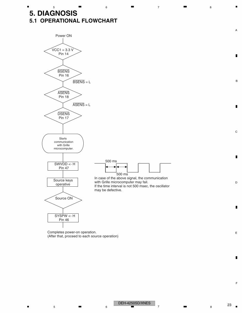
5. DIAGNOSIS5.1 OPERATIONAL FLOWCHART
VCC1 = 3.3 VPin 14
BSENSPin 16
ASENSPin 18
BSENS = L
Startscommunication
with Grillemicrocomputer.
SWVDD <- HPin 47
Source keysoperative
Source ON
SYSPW <- HPin 46
500 ms
500 ms
Completes power-on operation.(After that, proceed to each source operation)
In case of the above signal, the communicationwith Grille microcomputer may fail.If the time interval is not 500 msec, the oscillatormay be defective.
Power ON
ASENS = L
DSENSPin 17
DEH-4250SD/XNES 235 6 7 8
C
D
F
A
B
E
1 2 3 4
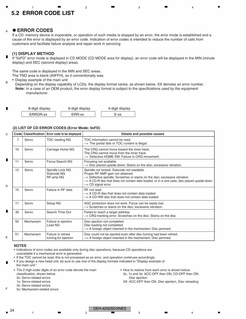
5.2 ERROR CODE LIST
8-digit display 6-digit display 4-digit display
ERROR-xx ERR-xx E-xx
(2) LIST OF CD ERROR CODES (Error Mode: 0xFD)
Code Classification Error code to be displayed Details and possible causes
10 Servo Carriage Home NG The CRG cannot move toward the inner track.The CRG cannot move from the inner track.--> Defective HOME SW; Failure in CRG movement.
7 Servo TOC reading NG TOC information cannot be read. --> The partial disk or TOC content is illegal.
11 Servo Focus Search NG Focusing not available--> Disc placed upside-down; Stains on the disc; excessive vibration.
17 Servo Setup NG AGC protection does not work. Focus can be easily lost.--> Scratches or stains on the disc; excessive vibration.
15 Servo Failure in RF data RF not read--> A CD-R disc that does not contain data loaded--> A CD-RW disc that does not contain data loaded
12 Servo Spindle Lock NGSubcode NGRF-amp NG
Spindle not locked. Subcode not readable.Proper RF AMP gain not obtained.--> Defective spindle; Scratches or stains on the disc; excessive vibration.--> A CD-R disc that does not contain data loaded, or in a rare case, disc placed upside-down.--> CD signal error.
30 Servo Search Time Out Failed to reach a target address--> CRG tracking error; Scratches on the disc; Stains on the disc
50 Mechanism Failure in ejectionLoad NG
Disc ejection not completedDisc loading not completed--> A foreign object inserted in the mechanism; Disc jammed.
51 Mechanism Failure in retriedturning for ejection
Disc could not be ejected even after disc turning had been retried.--> A foreign object inserted in the mechanism; Disc jammed.
NOTES• Indications of error codes are available only during disc operations, because CD operations are unavailable if a mechanical error is generated.• If the TOC cannot be read, this is not processed as an error, and operation continues accordingly.• If you design a new head unit, be sure to use one of the display formats indicated in “Display example of the main unit.”
ERROR CODES
(1) DISPLAY METHODIf “0xFD” error mode is displayed in CD MODE (CD MODE area for display), an error code will be displayed in the MIN (minute display) and SEC (second display) areas.
The same code is displayed in the MIN and SEC areas.The TNO area is blank (#0FFH), as it conventionally was.• Display example of the main unit Depending on the display capability of LCDs, the display format varies, as shown below. XX denotes an error number. Note: In a case of an OEM product, the error display format is subject to the specifications used by the equipment manufacturer.
If a CD memory device is inoperable, or operation of such media is stopped by an error, the error mode is established and a cause of the error is displayed by an error code. Indication of error codes is intended to reduce the number of calls from customers and facilitate failure analysis and repair work in servicing.
• The 2 high-order digits of an error code denote the main classification, shown below. 0x: Servo-related errors 1x: Servo-related errors 3x: Servo-related errors 5x: Mechanism-related errors
• How to restore from each error is shown below. 0x, 1x and 3x: ACC-OFF then ON, CD-OFF then ON, Disc ejection 5X: ACC-OFF then ON, Disc ejection, Disc reloading
DEH-4250SD/XNES241 2 3 4

C
D
F
A
B
E
5 6 7 8
5.3 CONNECTOR FUNCTION DESCRIPTION
R/SW, FOUTPUT
ANTENNA
1 FL+2 FR+3 FL-4 FR-5 RL+6 RR+7 RL-8 RR-
9 NC10 NC11 NC12 NC13 ACC14 B.REM15 B.UP16 GND
16 14 12 10 8 6 4 2
15 13 11 9 7 5 3 1
WIRED REMOTE CONTROL
DEH-4250SD/XNES 255 6 7 8

C
D
F
A
B
E
1 2 3 4
6. SERVICE MODE6.1 DISPLAY TEST MODE
The information such as the system version is checked and the lighting of every segment on the display is checked.
[Operation key]
[Test item]
Test mode is started
System Version information is displayed
S $ $ $ $ # # #
$ PEG number For PEG123A, "123A" is displayed# System microcomputer version For Ver.7.01, "701" is displayed
Unit number information is displayed
U % % % % % % %
% System unit number For CWW1234, "CWW1234" is displayed
Display Version information is displayed(Both of Sys. and Disp.) Ver. 2.01 or later
D $ $ $ $ # # #
$ PEG number For PEG123A, "123A" is displayed# Display microcomputer version For Ver.7.01, "701" is displayed
(Both of Sys. and Disp.) less than Ver. 2.01D I S P $ $ $ $ # # #
$ PEG number For PEG123A, "123A" is displayed# Display microcomputer version For Ver.7.01, "701" is displayed
Media microcomputer Version information is displayed
M V $ $ # #
$ Major version# Minor version
Manufacture_ID information is displayed
M I D $ $ $ $ $ $ $ $
$ Manufacture ID
Display is normally updated
Usual product operation is implemented to outward appearances.
Display update is stopped
The screen gets still when entering this item.
Every segment lights up
Every segment including icons lights up.
Every segment goes out
Every segment including icons goes out.
Only /UC model (excluding DEH-3200UB/XNUC)
Corresponding key Processing Remarks
CLK/DISP OFF + LIST Switching to next test display Also used as an entry key
DEH-4250SD/XNES261 2 3 4

C
D
F
A
B
E
5 6 7 8
6.2 CD TEST MODE
[Key]
Contents
Display
[BAND]
Power On(T.Offset is adjusted)TRK MIN SEC00 00 00
[2]
RF AMPGain switching
GG GG GG
*1
[3]
Focus CloseS curve check
TRK MIN SEC91 91 91
[6]
Focus Mode switching
0X 0X 0X
*2
[1]
Tracking ServoClose
00 00 00or 99 99 99
[<]
CRG +
[2]
Self-adjustingswitching
TRK MIN SEC?? ?? ??
*3*8
[>]
CRG -*8
[BAND]
Power Off
TRK MIN SEC
[BAND]
Power Off
TRK MIN SEC
[BAND]
Power Off
TRK MIN SEC
[BAND]
Power Off
TRK MIN SEC
[1]T.Close & AGC
Applicable servomechanism
TRK MIN SEC?tr ?min ?sec
[3]
RF AGC /RF AGC coefficient display
[<]
CRG +
8X 8X 8Xor 9X 9X 9X
[2]
T.Balance adjustment /T.BAL coefficient display
TRK MIN SEC?? ?? ??
[>]
CRG -
?? ?? ??
[1]
F,T,RF AGCF.Bias display switchingTRK MIN SEC
TRK MIN SEC
TRK MIN SEC
[3] [<]
CRG/TR Jump +
[2]
Tracking Open
[>]
CRG/TR Jump -
?tr ?min ?sec
TRK MIN SEC
TRK MIN SEC
00 00 00or 99 99 99
TRK MIN SEC?tr ?min ?sec
8X 8X 8Xor 9X 9X 9X
8X 8X 8Xor 9X 9X 9X
00 00 00or 99 99 99
TRK MIN SEC?tr ?min ?sec?? ?? ??
*7 F,T AGC / F.BiasRF AGC
8X 8X 8Xor 9X 9X 9X
[2]
Tracking Open
*6
*4 *4
Operation[Key] Test Mode
[BAND] Power On/Off[<] CRG + / TR Jump +
(Direction of the external surface)[>] CRG - / TR Jump -
(Direction of the internal surface)[1] T. CLS & AGC & Applicable servomechanism /
AGC,AGC display setting[2] RF Gain switching / Offset adjustment display /
T.Balance adjustment / T. Open[3] F. Close,S. Curve / Rough Servo and RF AGC /
F,T,RF AGC[6] F. Mode switching / Tracking Close
After the [EJECT] key is pressed keys other than the [EJECT] key should not be pressed, until disc ejection is complete.When the key [2] or [3] is pressed during the Focus Search, the power supply should be immediately turned off (otherwise the lens sticks to Wall, causing the actuator to be damaged).100TR Jump, the mechanism shall be set to the Tracking Close mode when the key is released.When the power is turned on/off the gain of the RFAMP is reset to 0 dB. At the same time all the self-adjusting values shall return to the default setting.Do not do Tracking Servo Close before doing Focus Servo Close. (Because the overcurrent flows)
- Flow Chart[CD] or [SOURCE]
Source ON
TRK MIN
[3] + [DISP] -> Reset
Test Mode IN
NOTEWhen a CD-DA (regular music CD) is played in the CD test mode, its sound quality will be temporarily deteriorated. The CD will then repeat normal, deteriorated, normal… playback. This is due to the difference in the playback modes between the normal operation mode and the CD test mode, and the interval of generating deteriorated mode and the time taken to return to the normal mode depend on the error of each clock.The time taken to turn to the deteriorated mode is at a minimum around 20 seconds while the time to return to the normal mode is maximum 40 seconds approximately.Make sure to check the sound quality in the normal operation mode.
*1) TYP t + 6 dB t + 12 dB TRK MIN SEC TRK06MIN06SEC06 TRK12MIN12SEC12
*2) Focus Close t S. Curve t F EQ measurement setting TRK00MIN00SEC00
TRK01MIN01SEC01 TRK02MIN02SEC02 (TRK99MIN99SEC99)
*3) F.Offset Display t T.Offset Display t Switch to the order of the original display
*4) 100TR Jump
*7) TRK/MIN/SEC t F.AGC t T.AGC Gain t F.Bias t RF AGC
*8) CRG motor voltage = 2 [V]
*9) TYP (1X) t 2X t 1X TRK MIN SEC
TRK22MIN22SEC22 TRK11MIN11SEC11*10) OFF(TYP) t FORCUS t TRACKING TRK MIN SEC
TRK70MIN70SEC70 TRK71MIN71SEC71
DEH-4250SD/XNES 275 6 7 8
C
D
F
A
B
E
1 2 3 4
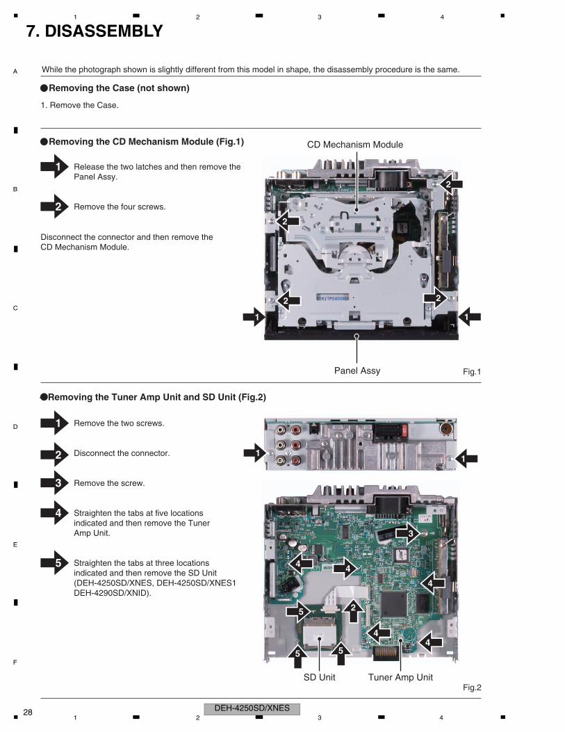
7. DISASSEMBLY
2
1
2
3
4
5
Fig.1
Fig.2
- Removing the CD Mechanism Module (Fig.1) CD Mechanism Module
- Removing the Tuner Amp Unit and SD Unit (Fig.2)
1. Remove the Case.
Remove the two screws.
Disconnect the connector.
Remove the screw.
Straighten the tabs at five locationsindicated and then remove the TunerAmp Unit.
Straighten the tabs at three locationsindicated and then remove the SD Unit(DEH-4250SD/XNES, DEH-4250SD/XNES1DEH-4290SD/XNID).
1
1
2
1
4
4
44
2
2
2
3
4
5 2
55
Disconnect the connector and then remove theCD Mechanism Module.
Tuner Amp UnitSD Unit
1 Release the two latches and then remove thePanel Assy.
Remove the four screws.
- Removing the Case (not shown)
Panel Assy
1
While the photograph shown is slightly different from this model in shape, the disassembly procedure is the same.
DEH-4250SD/XNES281 2 3 4

C
D
F
A
B
E
5 6 7 8
1. The seesaw button has ten hooks as shown in the figure below.
Front view
Oblique perspective figure2. Disconnect eight hools shown in the figure below and pull the seesaw button.
3. Pull the seesaw button forward.
Note: When you want to assemble the seesaw button in the grille by contraries, take care not to break the hook.
4.The seesaw button is disconnected from the grille.
- Removing the Grille Unit
DEH-4250SD/XNES 295 6 7 8

C
D
F
A
B
E
1 2 3 4
1. Hold the Upper and Lower Frames at the specified parts (circled with broken blue lines in the photo below).2. You can hold the tabs of the Lower Frame (circled with broken green lines in the photo below) if you do so only while lifting the Mechanism Unit from the table. Keeping the Mechanism Unit lifted by holding these tabs with your fingers may result in deformation.3. Be careful NOT to hold the front part of the Upper Frame or the CRG Mechanism and NOT to insert foreign objects into these mechanisms. Doing so may result in deformation.
Proper handling
Improper handling
How to Hold the Mechanism Unit
DEH-4250SD/XNES301 2 3 4
C
D
F
A
B
E
5 6 7 8
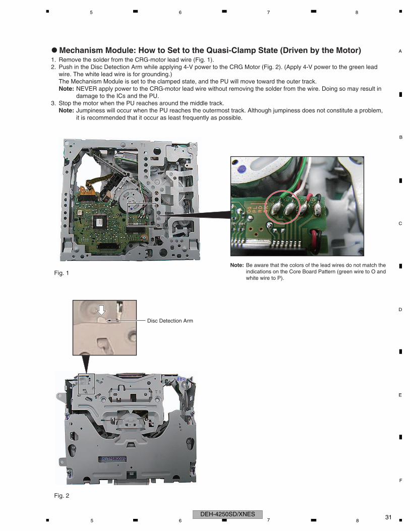
1. Remove the solder from the CRG-motor lead wire (Fig. 1).2. Push in the Disc Detection Arm while applying 4-V power to the CRG Motor (Fig. 2). (Apply 4-V power to the green lead wire. The white lead wire is for grounding.) The Mechanism Module is set to the clamped state, and the PU will move toward the outer track. Note: NEVER apply power to the CRG-motor lead wire without removing the solder from the wire. Doing so may result in damage to the ICs and the PU.3. Stop the motor when the PU reaches around the middle track. Note: Jumpiness will occur when the PU reaches the outermost track. Although jumpiness does not constitute a problem, it is recommended that it occur as least frequently as possible.
Fig. 1Note: Be aware that the colors of the lead wires do not match the indications on the Core Board Pattern (green wire to O and white wire to P).
Fig. 2
Disc Detection Arm
Mechanism Module: How to Set to the Quasi-Clamp State (Driven by the Motor)
DEH-4250SD/XNES 315 6 7 8

C
D
F
A
B
E
1 2 3 4
How to Remove the PU Unit
How to Move the PU toward the Outer Track
1. Set the unit to the quasi-clamp state, following the procedures described in “Mechanism Module: How to Set to the Quasi- Clamp State (Driven by the Motor).”2. Temporarily change the engagement position of the bias spring of the feed screw (Fig. 2b). Be careful not to cut yourself on the tip of the spring.3. Hold the PU unit by parts A in Fig. 1 then slide it toward the inner track.4. Remove the backend of the feed screw from the outer holder, by first sliding it, as shown in Fig. 3, then lifting it.5. Remove the PU unit, by lifting it. Lifting the PU unit will disengage the PU unit from the part B of the chassis.Note: When reassembling the PU unit, be sure to securely engage the PU unit with the part B of the chassis, as shown in Fig. 4. Also, be sure to change the engagement position of the bias spring of the feed screw to its original position (Fig. 2a). After reassembling, perform the PU adjustment, following the description in the service manual.
1. Set the unit to the quasi-clamp state, following the procedures described in “Mechanism Module: How to Set to the Quasi- Clamp State (Driven by the Motor).”2. Move the PU unit toward the outer track, by applying 1.5-V power to the CRG motor.Note: After moving the PU toward the outer track and taking the necessary measures, be sure to solder the lead wires.
Fig. 4
Fig. 3
Fig. 1
Fig. 2a Original engagement position
Fig. 2b Temporary engagement position
Slide toward the inner track.
One end of the spring is engaged beneath the resin flange and plate bend.
Outer holderBackend of the feed screw
Properly assembled state[Improper assembly]The chassis is not properly pinched by the PU case and PU rack.
A
B
DEH-4250SD/XNES321 2 3 4
C
D
F
A
B
E
5 6 7 8
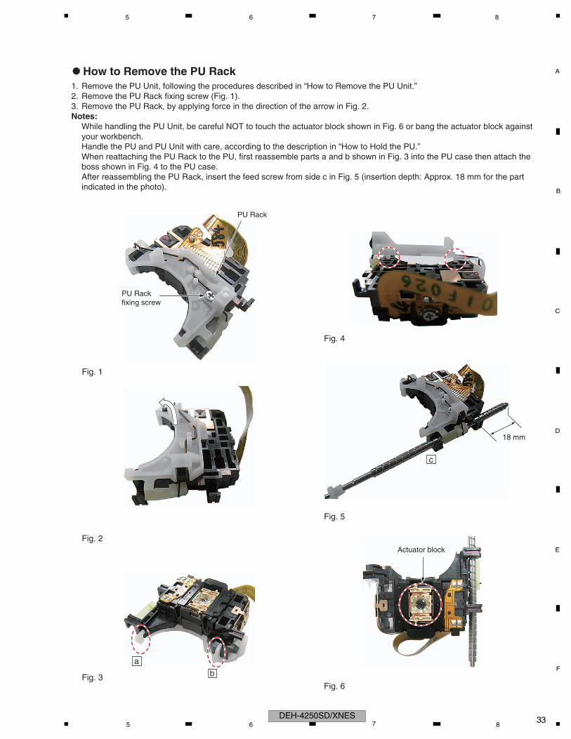
How to Remove the PU Rack1. Remove the PU Unit, following the procedures described in “How to Remove the PU Unit.”2. Remove the PU Rack fixing screw (Fig. 1).3. Remove the PU Rack, by applying force in the direction of the arrow in Fig. 2.Notes: While handling the PU Unit, be careful NOT to touch the actuator block shown in Fig. 6 or bang the actuator block against your workbench. Handle the PU and PU Unit with care, according to the description in “How to Hold the PU.” When reattaching the PU Rack to the PU, first reassemble parts a and b shown in Fig. 3 into the PU case then attach the boss shown in Fig. 4 to the PU case. After reassembling the PU Rack, insert the feed screw from side c in Fig. 5 (insertion depth: Approx. 18 mm for the part indicated in the photo).
Fig. 1
Fig. 2
Fig. 3
Fig. 4
Fig. 5
Fig. 6
PU Rack
PU Rack fixing screw
Actuator block
18 mm
b
c
a
DEH-4250SD/XNES 335 6 7 8

C
D
F
A
B
E
1 2 3 4
How to Hold the PU1. Be sure to hold the PU at the positions shown in “Proper handling.” NEVER hold it as shown in “Improper handling.”
Do not touch the object lens and ACT.
Do not touch the VR.
Do not touch the Hologram.
Do not pull the FPC.
Proper handling Improper handling
DEH-4250SD/XNES341 2 3 4

C
D
F
A
B
E
5 6 7 8
8. EACH SETTING AND ADJUSTMENT8.1 CD ADJUSTMENT
1) Cautions on adjustments In this product the single voltage (3.3 V) is used for the regulator. The reference voltage is the REFO1 (1.65 V) instead of the GND.If you should mistakenly short the REFO1 with the GND during adjustment, accurate voltage will not be obtained, and the servo’s misoperation will apply excessive shock to the pickup. To avoid such problems:a. Do not mix up the REFO1 with the GND when connecting the (-) probe of measuring instruments. Especially on an oscilloscope, avoid connecting the (-) probe for CH1 to the GND. b. In many cases, measuring instruments have the same potential as that for the (-) probe. Be sure to set the measuring instruments to the floating state.c. If you have mistakenly connected the REFO1 to the GND, turn off the regulator or the power immediately.
Before mounting and removing filters or leads for adjustment, be sure to turn off the regulator.
For stable circuit operation, keep the mechanism operating for about one minute or more after the regulator is turned on.
In the test mode, any software protections will not work. Avoid applying any mechanical or electrical shock to the mechanism during adjustment.
The RFAGC and RFO signals with a wide frequency range are easy to oscillate. When observing the signals, insert a resistor of 1k ohms in series.
The load and eject operation is not guarantied with the mechanism upside down. If the mechanism is blocked due to mistaken eject operation, reset the product or turn off and on the ACC to restore it.
2) Test modeThis mode is used to adjust the CD mechanism module. To enter the test mode.[3] + [DISP] -> Reset
To exit from the test mode.Turn off the ACC and back up.
Notes:a. During ejection, do not press any other keys than the EJECT key until the loaded disc is ejected.b. If you have pressed the (→) key or (←) key during focus search, turn off the power immediately to protect the actuator from damage caused by the lens stuck.c. For the TR jump modes except 100TR, the track jump operation will continue even if the key is released.d. For the CRG move and 100TR jump modes, the tracking loop will be closed at the same time when the key is released.e. When the power is turned off and on, the jump mode is reset to the single TR (91), the RF amp gain is set to 0 dB, and the auto-adjustment values are reset to the default settings.
When a CD-DA (regular music CD) is played in the CD test mode, its sound quality will be temporarily deteriorated. The CD will then repeat normal, deteriorated, normal… playback. This is due to the difference in the playback modes between the normal operation mode and the CD test mode, and the interval of generating deteriorated mode and the time taken to return to the normal mode depend on the error of each clock.The time taken to turn to the deteriorated mode is at a minimum around 20 seconds while the time to return to the normal mode is maximum 40 seconds approximately.Make sure to check the sound quality in the normal operation mode.
DEH-4250SD/XNES 355 6 7 8

C
D
F
A
B
E
1 2 3 4
8.2 CHECKING THE GRATING AFTER CHANGING THE PICKUP UNIT
FE
REFO1
CD CORE UNIT
Note :The grating angle of the PU unit cannot be adjusted after the PU unit is changed. The PU unit in the CD mechanism module is adjusted on the production line to match the CD mechanism module and is thus the best adjusted PU unit for the CD mechanism module. Changing the PU unit is thus best considered as a last resort. However, if the PU unit must be changed, the grating should be checked using the procedure below.
Purpose :To check that the grating is within an acceptable range when the PU unit is changed.
Symptoms of Mal-adjustment :If the grating is off by a large amount symptoms such as being unable to close tracking, being unable to perform track search operations, or taking a long time for track searching.
Method : Measuring Equipment Measuring Points
Oscilloscope, Two L.P.F. E, F, REFO1
Disc TCD-782 Mode TEST MODE
Checking Procedure1. In test mode, load the disc and switch the 3 V regulator on.2. Using the right and left buttons, move the PU unit to the innermost track.3. Press key 3 to close focus, the display should read "91". Press key 2 to implement the tracking balance adjustment the display should now read "81". Press key 3. The display will change, returning to "81" on the fourth press.4. As shown in the diagram above, monitor the LPF outputs using the oscilloscope and check that the phase difference is within 75 . Refer to the photographs supplied to determine the phase angle.5. If the phase difference is determined to be greater than 75 try changing the PU unit to see if there is any improvement. If, after trying this a number of times, the grating angle does not become less than 75 then the mechanism should be judged to be at fault. NoteBecause of eccentricity in the disc and a slight misalignment of the clamping center the grating waveform may be seen to "wobble" ( the phase difference changes as the disc rotates). The angle specified above indicates the average angle.
HintReloading the disc changes the clamp position and may decrease the "wobble".
100 kohm
390 pF
100 kohm
390 pF
E
VREF
F
VREF
Xch Ych
L.P.F.
L.P.F.
Oscilloscope
DEH-4250SD/XNES361 2 3 4

C
D
F
A
B
E
5 6 7 8
Grating waveform
45 degrees
0 degrees
75 degrees
60 degrees
30 degrees
90 degrees
Ech -> Xch 20 mV/div, ACFch -> Ych 20 mV/div, AC
DEH-4250SD/XNES 375 6 7 8

C
D
F
A
B
E
1 2 3 4
9. EXPLODED VIEWS AND PARTS LIST
9.1 PACKING
NOTES : Parts marked by " * " are generally unavailable because they are not in our Master Spare Parts List. The > mark found on some component parts indicates the importance of the safety factor of the part. Therefore, when replacing, be sure to use parts of identical designation. Screw adjacent to mark on the product are used for disassembly. For the applying amount of lubricants or glue, follow the instructions in this manual. (In the case of no amount instructions,apply as you think it appropriate.)
""
DEH-4250SD/XNES1
DEH-3200UB/XNUC
DEH-4250SD/XNES381 2 3 4

C
D
F
A
B
E
5 6 7 8
PACKING SECTION PARTS LIST
(2) CONTRAST TABLEDEH-4250SD/XNES, DEH-4250SD/XNES1, DEH-4290SD/XNID and DEH-3200UB/XNUC are constructed the same except for the following:
Owner's Manual,Installation Manual
Mark No. Description Part No.
1 Unit Box See Contrast table (2)
2 Contain Box See Contrast table (2)
3 Protector See Contrast table (2)
4 Protector See Contrast table (2)
5 Polyethylene Bag See Contrast table (2)
6 Cord Assy YDP5039
7 Accessory Assy See Contrast table (2)
8 Polyethylene Bag CEG1160
9 Handle CND3707
10 Screw See Contrast table (2)
11 Screw Assy See Contrast table (2)
* 12 Polyethylene Bag CEG-127
13 Screw TRZ50P080FTC
14 Screw See Contrast table (2)
15 Case Assy See Contrast table (2)
16 Remote Control Unit CXE2758
17-1 Owner's Manual See Contrast table (2)
17-2 Installation Manual See Contrast table (2)
* 17-3 Warranty Card See Contrast table (2)
* 17-4 Service Network See Contrast table (2)
* 18 Service Network See Contrast table (2)
Mark No. Description Part No.
Mark No. Description DEH-4250SD/XNES DEH-4250SD/XNES1 DEH-4290SD/XNID DEH-3200UB/XNUC 1 Unit Box CHG7062 CHG7063 CHG7064 CHG7118 2 Contain Box CHL7062 CHL7063 CHL7064 CHL7118 3 Protector CHP3931 CHP3931 CHP3931 CHP3941 4 Protector CHP3932 CHP3932 CHP3932 CHP3942 5 Polyethylene Bag QEG3001 QEG3001 QEG3001 CEG1173
7 Accessory Assy YEA5084 YEA5084 YEA5084 *YEA5071 10 Screw Not Used Not Used Not Used BPZ20P060FTC 11 Screw Assy YEA5082 YEA5082 YEA5082 YEA5072 14 Screw Not Used Not Used Not Used CRZ50P090FTC 15 Case Assy YXB5009 YXB5009 YXB5009 Not Used
17-1 Owner's Manual CRD4434 CRD4434 CRB3094 CRD4457 17-2 Installation Manual CRD4437 CRD4437 Not Used CRD4458* 17-3 Warranty Card Not Used CRY1250 CRY1304 CRY1276* 17-4 Service Network Not Used Not Used CRY1305 Not Used* 18 Service Network Not Used CRY1251 Not Used Not Used
Part No. Language
CRD4434 English, Spanish(Espanol), Portuguese(B), Traditional Chinese, Arabic
CRD4437 English, Spanish(Espanol), Portuguese(B), Traditional Chinese, Arabic
CRB3094 English
CRD4457 English, French, Spanish(Espanol)
CRD4458 English, French, Spanish(Espanol)
DEH-4250SD/XNES 395 6 7 8
C
D
F
A
B
E
1 2 3 4
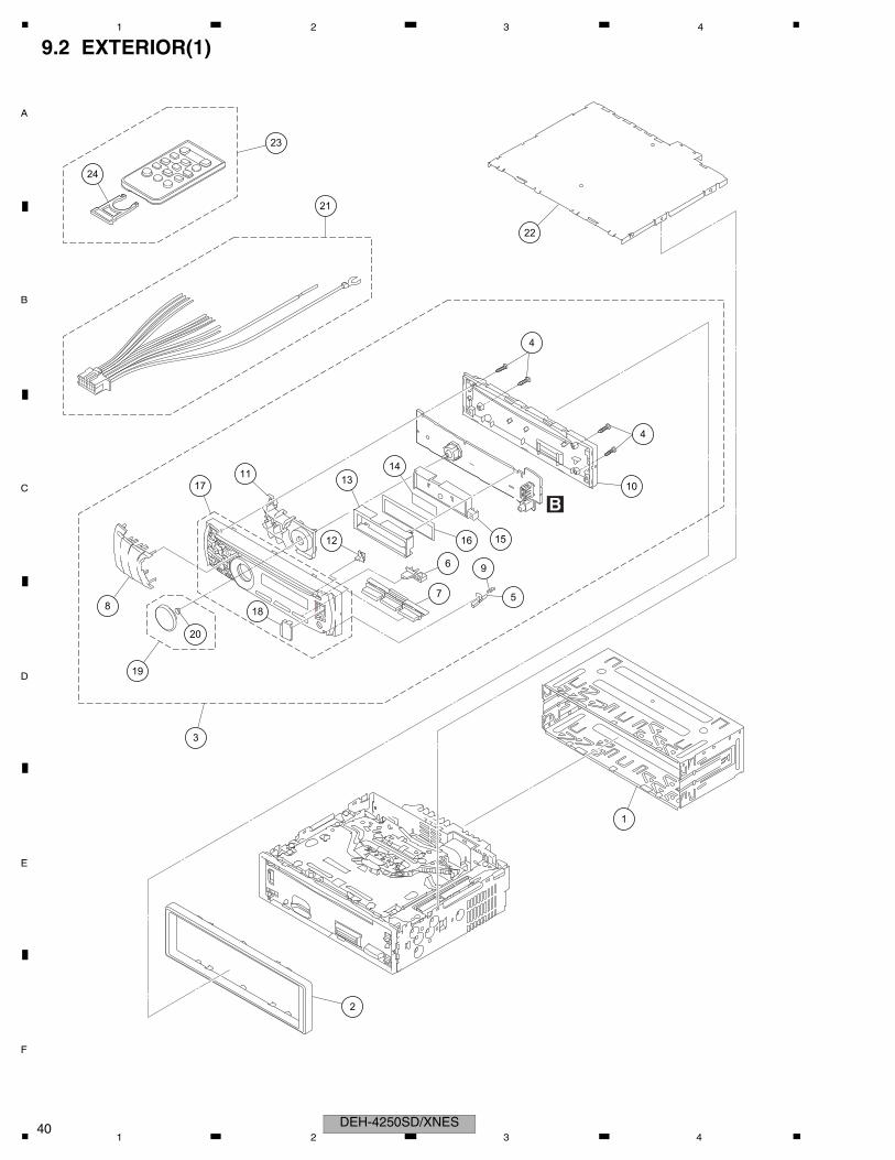
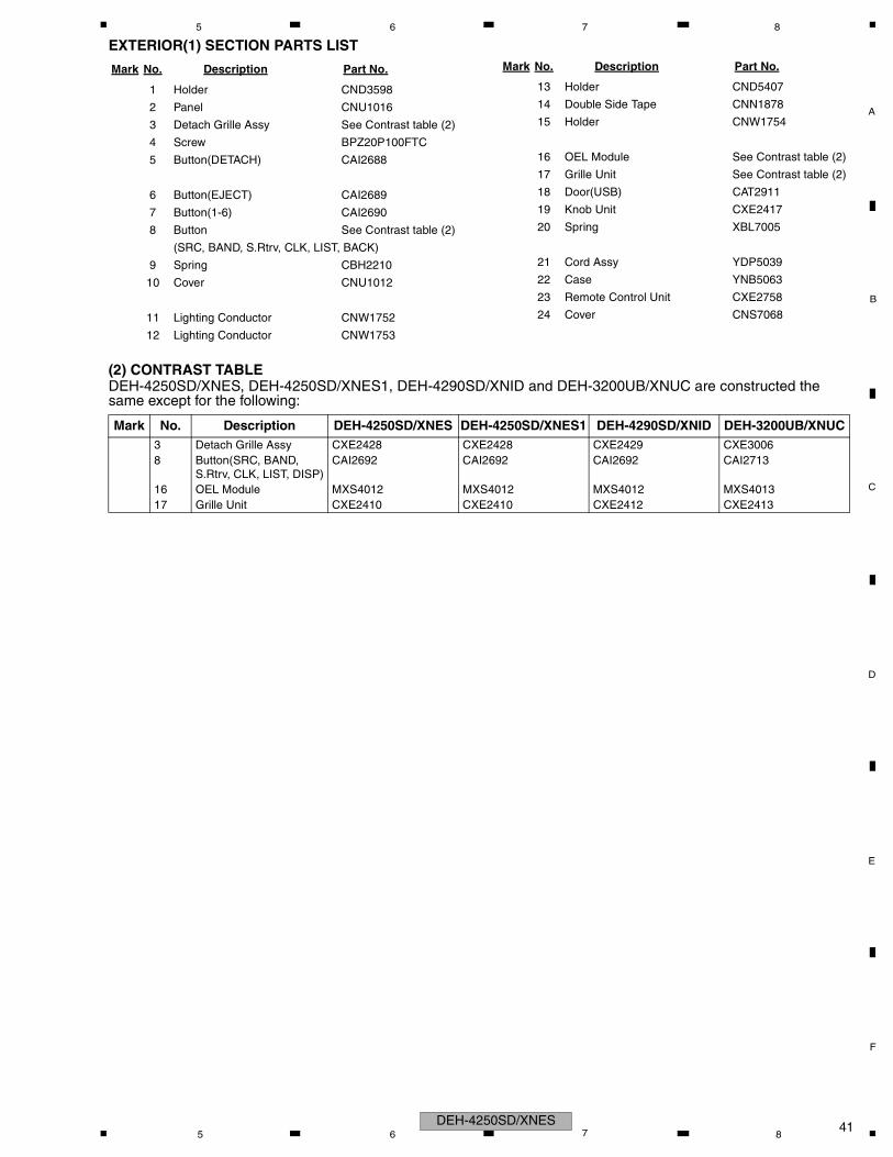
9.2 EXTERIOR(1)
B
DEH-4250SD/XNES401 2 3 4
C
D
F
A
B
E
5 6 7 8
EXTERIOR(1) SECTION PARTS LIST
(2) CONTRAST TABLEDEH-4250SD/XNES, DEH-4250SD/XNES1, DEH-4290SD/XNID and DEH-3200UB/XNUC are constructed the same except for the following:
Mark No. Description Part No.
1 Holder CND3598
2 Panel CNU1016
3 Detach Grille Assy See Contrast table (2)
4 Screw BPZ20P100FTC
5 Button(DETACH) CAI2688
6 Button(EJECT) CAI2689
7 Button(1-6) CAI2690
8 Button See Contrast table (2)
(SRC, BAND, S.Rtrv, CLK, LIST, BACK)
9 Spring CBH2210
10 Cover CNU1012
11 Lighting Conductor CNW1752
12 Lighting Conductor CNW1753
13 Holder CND5407
14 Double Side Tape CNN1878
15 Holder CNW1754
16 OEL Module See Contrast table (2)
17 Grille Unit See Contrast table (2)
18 Door(USB) CAT2911
19 Knob Unit CXE2417
20 Spring XBL7005
21 Cord Assy YDP5039
22 Case YNB5063
23 Remote Control Unit CXE2758
24 Cover CNS7068
Mark No. Description Part No.
Mark No. Description DEH-4250SD/XNES DEH-4250SD/XNES1 DEH-4290SD/XNID DEH-3200UB/XNUC 3 Detach Grille Assy CXE2428 CXE2428 CXE2429 CXE3006 8 Button(SRC, BAND,
S.Rtrv, CLK, LIST, DISP)CAI2692 CAI2692 CAI2692 CAI2713
16 OEL Module MXS4012 MXS4012 MXS4012 MXS4013 17 Grille Unit CXE2410 CXE2410 CXE2412 CXE2413
DEH-4250SD/XNES 415 6 7 8

C
D
F
A
B
E
1 2 3 4
9.3 EXTERIOR(2)
DEH-4250SD/XNESDEH-4250SD/XNES1DEH-4290SD/XNID
A
B
BA
AD
C
C
DEH-4250SD/XNES421 2 3 4

C
D
F
A
B
E
5 6 7 8
EXTERIOR(2) SECTION PARTS LIST
(2) CONTRAST TABLEDEH-4250SD/XNES, DEH-4250SD/XNES1, DEH-4290SD/XNID and DEH-3200UB/XNUC are constructed the same except for the following:
Mark No. Description Part No.
1 Screw ASZ26P050FTC
2 Screw BSZ26P060FTC
3 Screw BSZ26P100FTC
4 Cable CDE9106
5 Cable See Contrast table (2)
6 Chassis CNA3151
7 Earth Plate CNC8915
8 Cushion CNM8890
9 Insulator CNN3145
10 Tuner Amp Unit See Contrast table (2)
11 Screw BPZ26P080FTC
12 Screw BSZ26P060FTC
13 Screw BSZ26P160FTC
14 Holder CND5411
15 Holder CND5423
16 FM/AM Tuner Unit CWE2098
17 Holder CND4324
> 18 Fuse(10 A) YEK5001
19 Heat Sink YNR5139
20 SD Unit See Contrast table (2)
21 Holder See Contrast table (2)
22 Button CAC4836
23 Spring(Thin) CBH2961
24 Spring(Thick) CBH2962
25 Panel See Contrast table (2)
26 Arm CNV9312
27 Arm CNW1439
28 Spring YBH5012
29 Cover YNN5030
30 CD Mechanism Module(S11) CXK5800
31 Holder YND5048
Mark No. Description Part No.
Mark No. Description DEH-4250SD/XNES DEH-4250SD/XNES1 DEH-4290SD/XNID DEH-3200UB/XNUC 5 Cable CDE9107 CDE9107 CDE9107 Not Used 10 Tuner Amp Unit CWN4805 CWN4805 CWN4805 CWN5219 20 SD Unit CWN4816 CWN4816 CWN4816 Not Used 21 Holder CND5417 CND5417 CND5417 Not Used 25 Panel CNU1015 CNU1015 CNU1015 CNU1017
DEH-4250SD/XNES 435 6 7 8

C
D
F
A
B
E
1 2 3 4
9.4 CD MECHANISM MODULE
A
CD
C
A
B
B
C
D
(A) : GEM1045
(B) : GEM1038
(C) : GEM1024
(D) : GEM1043
(C)
(C)
(A)
(A)
(D)
(D)
(A)
(A)
(D)
(A) (A)
(A)
(A)
(A)
(C)
(C)
(C)
(C)
(B)
(C)
(C)
DEH-4250SD/XNES441 2 3 4

C
D
F
A
B
E
5 6 7 8
CD MECHANISM MODULE SECTION PARTS LIST
Mark No. Description Part No.
1 Screw BMZ20P020FTC
2 Screw BSZ20P040FTC
3 Screw(M2 x 4) CBA1835
4 Washer CBF1038
5 Spring CBH3010
6 Spring CBH2855
7 Spring CBH2856
8 Spring CBH2860
9 •••••
10 Spring CBH3011
11 Spring CBH3012
12 Spring CBH3014
13 Spring CBH3015
14 Spring CBH3016
15 Spring CBH3017
16 Spring CBH3018
17 Spring CBH3019
18 Spring CBH3020
19 Spring CBL1797
20 Pickup Unit(S10.5)(Service) CXX1942
21 Bracket CND4553
22 Arm CND4555
23 Frame CND4557
24 Frame CND5217
25 Lever CND5398
26 Sheet CNN2280
27 Rack CNV8342
28 Guide CNW1171
29 Roller CNW1172
30 Arm CNW1173
31 Arm CNW1174
32 Roller CNW1175
33 Lever CNW1176
34 Arm CNW1177
35 Arm CNW1178
36 Gear CNW1180
37 Gear CNW1181
38 Gear CNW1182
39 Gear CNW1183
40 Rack CNW1184
41 Gear CNW1185
42 Gear CNW1186
43 Gear CNW1187
44 Gear CNW1188
45 Clamper CNW1190
46 Arm CNW1192
47 Holder CNW1193
48 Holder CNW1194
49 Damper CNW1197
50 Damper CNW1198
51 Arm CNW1726
52 Motor Unit(M2)(LOAD/CRG) CXC4026
53 Screw Unit CXC8894
54 Arm Assy CXC8896
55 Washer CBF1037
56 Washer CBF1038
57 Arm CND4554
58 Collar CNV6906
59 Roller CNW1196
60 Gear Unit CXC8893
61 Washer YE15FTC
62 Chassis Unit CXE1946
63 Motor Unit(M1)(SPDL) CXE2273
64 Screw JFZ20P025FTC
65 Screw JGZ17P022FTC
66 Screw IMS20P030FTC
67 CD Core Unit (S11STD-DOUT) CWX3774
Mark No. Description Part No.
DEH-4250SD/XNES 455 6 7 8

C
D
F
A
B
E
SS
EN
S
DS
EN
ST
ELI
N
ME
DS
TB
Y
RO
T0
RO
T1
SYS8V
D602RB751S-40
601
37 38 39 40 41 42848586878889
R61
6
100k
R
100k
R60
810
0k
R624 47k
R61
7
R626 10k
EP
M
SO
R10
INF
R11
INR
R12
INP
R13
OU
TP
R14
OU
TR
R27
OU
TP
L
28IN
PL
29IN
RL
30IN
FL
31S
OL
MP
LC
219
1u/1
0
C22
1
NM
1u/1
0
C22
2
NM
ME
DS
TB
Y
NC
TE
LIN
PC
L
NC
.MICRO
AS
EN
BO
VDD
BUP
SYS
NC
NC
NC
NC
VDD
R6
100k
R627
1 2 3 4
10. SCHEMATIC DIAGRAM10.1 TUNER AMP UNIT 1/2 [MAIN] (GUIDE PAGE)
A-a A-b
A-a A-b
A-bA-a
Large sizeSCH diagram
Guide page
Detailed page
Note: When ordering service parts, be sure to refer to " EXPLODED VIEWS AND PARTS LIST" or "ELECTRICAL PARTS LIST".
1/2A
A-a 1/2
DI
ROT0
ROT1
PEE
PEE
DSENS
ASENS
BSENS
MEDRST
SY
Sto
SH
SL
SS
EN
S
KE
YA
D
SY
NC
FLG
uCOM_BUS
VDCONT
FLG
USBCTL
DP
DT
DP
DT
KY
DT
KY
DT
RW
CLK
SYNC
KEYD
KEYAD
POWER_BUS
DD5V
KE
YD
KE
YD
TUNR
TUNL
TUNL
CDL
TUNR
CDR
USB5V
DM
DP
AUXL
AUXR
RDSLK
RDS57K
RCK
RDT
SH
toS
YS
US
BC
TL
CE2
CE1
CK
DO
LDET
SYS8V
SL
BUP
RESET
RESET
RWCNVSS
VDD5V
VDD33
AUXR
AUXG
AUXL
AUXG
NMBZ601
11
22
JA661CKS4124
231
CKS6188-ACN801
1
2
3
4
5
6
7
8
9
10
11
12
13
14
15
16
17
18
19
20
220u
C16
1
CC
H18
04-A
C16
6
C610 0.1u/10
C606
0.1u/10
C15
1
0.1u
/10
C15
2
0.1u
/10
C60
7
NM
1u/10C211
1u/10C212
2.2u/10C203
1u/10C202
1u/10C201
C40
3 NMC
401
0.01
u/10
C40
5
0.01
u/10
C16
4
NM
C16
3
0.1u
/16
C16
7
220p
/50
C16
2
1u/1
6
C40
2
CC
G11
92-A
C40
6
NM
C43
14.
7u/6
.3
C40
4
NM
C43
2
0.01
u/50
C210 0.22u/16
C209 0.22u/16
D432
NM
D431
NM
D161
CRG03
D601
RB551V-30
D16
3
CM
S02
GND GND
GND
GND
GND
GND
GND
GND
GND
GND
GND
GND
GND
GND
GND
GND
NJM2885DL1-33IC431
1IN
2G
ND
3O
UT
BD9781HFPIC161
1V
IN2
SW
3R
T4
GN
D5
FB
6IN
V7
EN
IC151
R5523N001B
EN1
GND2
FLG3
VIN4
5VOUT
IC
1
2
3
4
5
BYTE6
CNVSS7
8
9
RESET10
XOUT11
VSS112
XIN13
VCC114
15
16
17
18
19
20
21
22
23
24
25
26 27 28 29 30 31 32 33 34 35 36909192939495
VR
EF
96A
VC
C97989910
0
M2R6TP_GNDKN401
L602
L151
NM
L161CTH1253-A
L401
BTH1100-A
L402 BTH1100-A
Q40
2
NM
1E
1
2B
13
C2
4E
2
5B
2
6C
1
Q40
1
NM
1E
1
2B
13
C2
4E
2
5B
2
6C
1
R409
NM
2
1
4
3 6
5
8
7
R809 1
R811
8.2
R810
8.2
R808 2.2kR408
1.5k
R406 680
R403 680
R402 NM
R407 680
R401 680
R405 680
R404 680
R804 2.2k
R801 2.2k
R805 2.2k
R802 2.2k
R16
5
100k
R613 100k
R16
8
470
R16
7
33k R
162
NM
R16
1
100k
R615
100k
R60
710
0k
R662 1k
R661 1k
R605 100k
R606
2.2k
R61
010
0k
R60
910
0k
R15
1
100k
R16
4
NM
R16
3
68k
R614 100k
R604
100
R60
3
1M
R601
NM
KEYD
KEYAD
DSENS
PC
L1
DP
VBUS
AUXL
OELG
SSENS
ROT0
DPDT
DM
ILMG
DGND
CNVSS
RESET
DP
DT
2
KY
DT
2
RW
CLK
KE
YD
2
AUXG
AUXR
SWVDD
KYDT
USB5V
VA
661
VR
105C
5R0A
AA
VA
662
VR
105C
5R0A
AA
USB5V
DD5V
ZN
R40
1
IMS
A-6
802-
01Y
900-
T
uCOM_BUS
POWER_BUS
D162
CRG03
D16
4
NM
R16
6
24k
C16
5
0.01
u/10
C43
3
4.7u
/10
R803 2.2k
C604
10p/50
C605
12p/50
IC20
1
S1Q
+R
1
S2A
-R2
S3A
+R
3
S4B
-R4 5
S5B
+R
6S
6R7
MN
R8
MP
R9
3233M
NL
34S
6L
35S
5B+
L
36S
4B-L
37S
3A+
L
38S
2A-L
39S
1Q+
L
40Q
CO
M
R20
5
NM
R20
6
NM GND
C22
0
USBG
ROT1
ILM+B
GND
OEL+B
R20
7
22k
R20
8
22k
R814100
R816 100
L801
CTF1713-A
1 2
34
GND
GND
DDIN
R62
7
100k
R62
8
100k
U40
1
1AMANT
2RFGND
3FMANT
4VCC
5SL
6CE2
7NC1
8CE1
9CK
10DI
11LDET
12OSCGND
13ROM_VDD
14DO
15DGND
16NC2
17VDD_3.3
18RDS_CK
19RDS_DATA
20RDS_LOCK
21RDS_HSLK
22AGND
23Lch
24Rch
L404
BTH1104-A
L403
NM
C40
7
0.01
u/10
C40
8
CC
G11
92-A
R16
9
120
TUN3V
X60
1C
SS
1795
-A
X1
1G
ND
12
GN
D2
4X
23
R602 4.7k
GND
VA
807
VR
105C
5R0A
AA
VA
808
VR
105C
5R0A
AA
VA
806
VR
105C
5R0A
AA
VA
801
VR
105C
5R0A
AA
VA
802
VR
105C
5R0A
AA
VA
803
VR
105C
5R0A
AA
GND
D80
1D
Z2S
068C
D80
2D
Z2S
068C
D80
3
DZ
2S06
8C
D80
4
DZ
2S06
8C
D80
5
DZ
2S06
8C
R202
330
VA811
NM
1
1
2
2
3
3
4
4
5
5
6
6
JA401CKX1070-A
12
3
C801
0.1u/16
R63
1
100k
R63
2
100k
C80
2
1u/1
6
TUNG
FM
/AM
TU
NE
R U
NIT
RF
TUNER
ILM
CW
E20
98-
X-2
026
ILM
GRILL
TUNER3V REG
E.VOL
NM
D
A
D
A
VD
D5
BU
P
KE
YD
NC
NC
ME
D_R
X
NC
MO
DE
L1SL
BSENS
US
BC
TL
NC
PEE
NC
ASENS
ROT0
SYNC
ROT1
NC
ME
D_T
X
USBFLG
NC
AANT
VDCONT
DP
DT
NC KY
DT
NC
SYS
SS
EN
S
20.0
00M
Hz
AV
SS
NC
NC
MEDRST
DSENS
KE
YA
D
VD
D3.
3
SY
S8V
VDD3.3
BUP
SYS8V
NC
DDCON
NC
D-
ROT1
KYDT
ILMG
DPDT
OELG
D+
USBG
USBG
ROT0
AUX R
DGND
AUX G
AUX L
VBUS
SOURCE
SW3.3V
OEL+B
ILM+B
DSENS
USB ILM
1608
(Black)
WIRED REMOTE
NC
MO
DE
L2
1608
1608
1608
TUNL
AUXG
CDL
CDR
TUNR
AUXR
AUXL
10U
/10
10U
/10
1608
1R0u
1R0u
BLM15AG102SN1
D
F
(15uH)
(150
u)
1608
VDD5
VD
D5
BU
P
VD
D3.
3
SY
S8V
SY
S8V
A
OEL
1608
VD
D3.
3
D
IC601
*
CWW1965-/PEG640A8
1608
*
5.13V
5.13V
3.29V
2/2A
BCN1801
A:DEH-4250SD/XNESB:DEH-4250SD/XNES1C:DEH-4290SD/XNIDD:DEH-3200UB/XNUC
FM(30%):-24.00 dBsAM(30%):-24.00 dBs
FM:-24.00 dBsAM:-24.00 dBs
AUX: +2.20 dBsCD/USB/SD: +3.04 dBs
DEH-4250SD/XNES461 2 3 4

C
D
F
A
B
E
SY
Sto
SH
SL
KE
YA
D
KY
DT
RW
CLK
KE
YD
SH
toS
YS
30 31 32 33 3492939495
VR
EF
96
R81
8.
R81
8.
R808 2.2k
R804 2.2k
R801 2.2k
R805 2.2k
R802 2.2k
RW
CLK
KE
YD
2
R803 2.2k
S S3A
+R
3
S4B
-R4 5
S5B
+R
6S
6R7
3435S
5B+
L
36S
4B-L
37S
3A+
L
38S
2A-L
S1Q
+L
L801
CTF1713-A
2
3
ND
OL
KE
YD
ME
D_R
X
MO
DE
L1SL
NC
ME
D_T
X
KY
DT
S
AV
SS
KE
YA
D
1608
16
1608
IC601
CWW1965-/PE
16
5 6 7 8
1/2A
A-b 1/2
RR2
RL2
RR1
RL1
FR2
FR1
FL1
FL2
RR2
RR1
FR2
FR1
FL1
FL2
RL1
RL2
TELIN
RESET
FR
FL
RR
RL
SWR
SWL
DALMON
CE1
CE2
LDET
DO
RDSLK
FR
RR
RL
FL
BSENS
ASENS
ISENS
SS
EN
S
DI
SW
VD
D
MU
TE
VC
K
DS
EN
ST
ELI
N
SS
EN
S
ISE
NS
VCK
VDT
VST
DP
DT
RW
CN
VS
S
RE
SE
T
KY
DT
DA
LMO
N
KE
YD
RW
CLK
ME
DS
TB
Y
ME
DM
UT
E
MUTE
SY
SP
W
SY
SP
W
SYSPW
KE
YD
VS
T
VD
T
DA
LMO
N
DA
LMO
N
KY
DT
SW
VD
D
ILM
PW
OE
LPW
FL
RL
SWL
FR
RR
SWR
RO
T0
RO
T1
DM
DP
OE
LPW
RCK
SYSPW
ILM
PW
DP
DT
SDCTL
US
BC
TL
RD
S57
K
RD
T
SYS8V
SG001528
CK
JA981CKM1586-A
1
2
3
4
5
6
7
8
9
10
11
12
14
15
16
17
18
13
CCH1486-A
C361
22u/
16
C38
1
220u
/10
C91
1
100u
/16
C91
3
1000
u/16
C90
1
C609
NM
C608 0.1u/10
C60
2
NM
C358 0.47u/16
C355 0.47u/16
C64
1
NM
C362
0.1u/16
C94
1
0.04
7u/1
6
C93
1
NM
C90
3
NM
C356 0.47u/16
C363
2.2u/10
C364
2.2u/10
C366
NM
C90
2
0.01
u/10
C357 0.47u/16C353 0.47u/10
C60
1
CC
G11
92-A
C302
CCG1192-A
C303
NM
C301
CCG1192-A
C304
NM
C306
CCG1192-A
C305
CCG1192-A
C65
1
1u/1
0
C352 0.47u/10
C36
7
CC
G11
92-A
C90
4
CC
G11
92-A
C351 0.47u/10
C31
1
NM
C21
4C
CG
1192
-A
C365
10u/35
C21
8
CC
G11
92-A
C21
3C
CG
1203
-A
C84
1
NM
C84
2
NM
C21
50.
1u/1
0
C91
2
NM
C951
NM
C31
2
NM
C30
7
NM
C30
9
NM
C30
8
NM
C31
0
NM
C90
6
NM
C354 0.47u/10
D931
NM
D901CRG03
D94
1C
RG
03
D98
1
CR
G03
D94
2
CR
G03
D98
2
CR
G03
D65
1
1SS
352-
TR
B
D383
1SS352
D602RB751S-40
D382
DAN202U
D951NM
D922
HZU7L(A1)
D381
UDZS8R2(B)
D921
HZU7L(C3)
GND
GND
GND
GND
GND
GND
GND
GND
GND
GND
GND
GND
GND
GND
GND
GND
GND
GND
GND
GND
GND
GND
GND
GND
GND
GND
GND
GND
IC651
S-80827CNNB-B8M
OUT1
VDD2
NC3
VSS4
IC641
CS1
SK2
DI3
DO4 5
GND
6TEST
7NC
8VCC
IC601
35 36 37 38 39 40 41 42 43 44 45 46 47 48 49 50
51
52
53
54
55
56
57
58
59
60
61
62
63
64
65
66
67
68
69
70
71
72
73
74
75
76777879808182838485868788899091
NJM2388F84IC911
1V
IN
2V
OU
T
3G
ND
4C
ON
TR
OL
JA301
1
2
3
4
5
6
7
8
9
10
L603
L601BTH1103-A
L841NM
L201
NM
L951
min
iSM
DC
075F
/24
P30
11
2
LTC114EUBQ361
NMQ931
RT3T22M
Q902
E1 1
B1 2
C2 3 E24
5 B2
6 C1
RT3T22M
Q382
E11
B12
C23E2 4
5B2
6C1
Q3812SC4081(RS)
Q9012SD2396(K)
NMQ951
R20
1
1k
21 436 58 7
R61
6
100k
R813
100k
R812
100k
R809 100k
1
2
0
2
R642
NM
R64
1
NM
R643
100k
R61
94.
7k
R384
47kR383
47k
R38
1
47k
R382
100k
R361
10kR
362
10k
R363
330
R911
1k
R91
2
47k
R313
NM
R31
4
NM
R316
0
R385
1k
R304
NM
R823
10k
R951
NM
R922
10k
R921
100k
R92
5
4.7k
R92
3
47k
R92
4
47k
R931
NM
R306
820
R60
810
0k
R65
1
100k
R652
1.5k
R844
10k
R84
3
1k
R84
2
4.7k
R301
820
R365
10k
R622
NM
R303
NM
R30
8
22k
R629
NM
R624 47k
R30
9
NM
R305
820
R31
1
22k
R31
2
22k
R30
7
22k
R31
0
NM
R621
NM
R61
7
100k
R61
810
0k
R620
100k
R623 100k
R821
1
R626 10k
R315
0
R302
820
R364
NM
R90
1
3.3k
R90
2
22k
R84
1
NM
CS
G10
20-A
S65
11
2
RESET2
VDD2
8VCNT
BUP1
GND2
BUP2
GND1
RR
RL
SWL
SWR
FL
FR
MUTE1
VDD33V
RCAG
BSEN1
VDD5VPC
L1
BSEN2
TEL1
ASENS
MUTE3
SYS+B
RL2
RR2
ILL1
FL1
EP
M
ME
DM
UT
E CE
ACC1
RR1
FR2
FL2
RL1
FR1
BRE1
TEST1
VDD33
SYS8V
BUP
VDD5V
R926
1k
R932
NM
C92
1
0.1u
/16
C93
2
NM
R954
NM
D90
2
UD
ZS
5R6(
B)
RT
3CLL
M(E
F)
Q92
1
E1
1 B1
2 C2
3E
245B
26C
1
C90
5
4.7u
/6.3
C90
7
4.7u
/6.3
C60
3C
CG
1201
-A
GND
NMQ362
R952
NM
NMCN601
12345678910
DA
LMO
N
GND
Q8312SD1664(R)
R833
1.2k
C83
1
0.04
7u/1
6
RT3T22M
Q832
E1 1
B1 2
C2 3 E24
5 B2
6 C1R83
1
10k
R832
1
D83
1
HZ
U10
(B1)
LTC114EUBQ842
LSA1576UBQ841
LTC114EUBQ822
R82
2
4.7k
2SA1036K(QR)Q821
BD
3733
FV
MN
R8
MP
R9
SO
R10
INF
R11
INR
R12
INP
R13
OU
TP
R14
OU
TR
R15
OU
TF
R16
GN
D17
VR
EF
18V
CC
L19
FIL
H20
VC
CH
21S
TB
22C
LK
23D
AT
A
24D
GN
D
25O
UT
FL
26O
UT
RL
27O
UT
PL
28IN
PL
29IN
RL
30IN
FL
31S
OL
32M
PL
33M
NL
S6L
R203
NM
C21
70.
1u/1
0
C21
6C
CG
1203
-A
C21
9
1u/1
0
C22
1
NM
C22
0
1u/1
0
C22
2
NM
RT3T22M
Q363
E11
B12
C23E2 4
5B2
6C1
R36
6
10k
VDD1
R834
NM
L981
D903
NMIC901
S-1132B33
VOUT1
VSS2
NC3
SW4
5VIN
C368NM
C369NM
IC351PA2030A
TAB1
PW-GND22
OUT2(-)3
STBY4
5OUT2(+)
6VCC2
7OUT1(-)
8PW-GND1
9OUT1(+)
10RIPPLE
11IN1
12IN2
15IN3
16AC-GND
17OUT3(+)
18PW-GND3
19OUT3(-)
20VCC1
21OUT4(+)
22MUTE
23OUT4(-)
24PW-GND4
25H-SW/VOS-DET
13PRE-GND
14IN4
TP70
TP69
R630
100k
C83
2
1000
p/50
NMQ302
E11
B12
C23
E24
5B2
6C1
UMH3NQ301
E11
B12
C23
E24
5B2
6C1
UMH3NQ303
E11
B12
C23
E24
5B2
6C1
REFERENCE AREA MAP sheet1
SWVDD
ROM COLECTIONTEL IN
VDD5 & VDD3.3
MECHA VD
SYS+B
ISENS
ILM+B
B.REMSYSTEM MICRO
SOURCE CONNECTOR
MECHA
RESET
ASENS&BSENS
GRILL
TUNER 3V REG
AUTO ANTENNA
A
ILM
NM
TUNER
IN3(FR)
IN1(FL)
IN4(RR)
IN2(RL)
RCAAMP
MED3.3V & MED1.2V
USB H.SW
MUTE
IP-BUS
3300/16105
10U
/10
D
FR
FL
SWVDD
ILM+B
TELMUTE
SYS+B
VDD5.0
MUTE
B.REM
AMP
ROM CORRECTION
RCA OUT
A
RR
RL
CONNECTORSOURCE
(2125)
BSENS&ASENS
RESET
BUP
NC
LDET
TUNPDI
VDT
ME
DS
TB
Y
SY
SP
W
ME
DM
UT
E
NC
ROMCS
DA
LMO
N
ILM
PW
VCK
US
BC
TL
ROMCK
VST
VCC
SW
VD
D
ROMDATA
TESTIN
TE
LIN
NC
TUNPDO
PC
L
NC
NC
TUNPCK
RDSLK
TUNPCE1
IPPW
RCK
RD
SD
T
YS.MICRO
SS
EN
S
AS
EN
BO
NC
VSS
NC
NC
OE
LPW
NC
NC
ISENS
VDD3.3
BUP
SYS8V
VD
D3.
3
SY
S8V
BUP
VDD5
SY
S8V
VD
D3.
3
SY
S8V
VDD3.3
VDD3.3
BUP
SYS8V
MU
TE
RD
S57
K
R632R631
No MOUNT
100K 1K
0.1u
E.VOL
MEDIA uCOMFLASH ROM
DAC & LPF
SD CONNECT
NC
TUNPCE2
NM
10U
/10
--
1608
NC
NC
NC
NC
ISE
NSN
C
NC
NC
NC
NC
NC
A
--
SWR
FR
SWL
FL
GND
GND
GND
GND
BU
P
VD
D3.
3
SVR
S-GND
SWITCH OUT
10U
/10
10U
/10
10U
/10
08
10uH
NM
10U/10
10U/10
10U/10
10U/10
10u/
10
ipod CP
BU
PB
UP
VDD3.3
VD
D5
VDD3.3
VDD5
D
VDD5
REFERENCE AREA MAP sheet2
WIRED REMOTE
ILM
BUP
OEL+B
10U
/10
DC-DC CONVERTOR OEL+B
NC
SD
CT
L
CCG1236-A
1608 16081608
*
100k -G640A8
08
NM
NM
NM
CTH1445
YKB5011-
R628
100k
R627
-
FUSE 10 A
600 uH
YE
K50
01
5.10V
3.30V
8.36V
9.17V
14.18V
3.24V
3.28V
>
TUNER AMP UNIT (MAIN)1/2AThe > mark found on some component parts indicatesthe importance of the safety factor of the part.Therefore, when replacing, be sure to use parts ofidentical designation.
Symbol indicates a resistor.No differentiation is made between chip resistors anddiscrete resistors.
NOTE :
Symbol indicates a capacitor.No differentiation is made between chip capacitors anddiscrete capacitors.
NM : No Mount
>
FM:+20.00 dBsAM:+20.00 dBs
AUX:+36.20 dBsCD/USB/SD:+36.04 dBs
FM: -6.00 dBsAM: -6.00 dBs
AUX:+10.20 dBsCD/USB/SD:+10.04 dBs
DEH-4250SD/XNES 475 6 7 8

C
D
F
A
B
E
CC
H14
86-A
C36
1
641
NM
C367
CCG1192-A
DA
N20
2U
D38
1
GN
D
GN
DG
ND
IC64
1
CS
1
SK
27
NC
8V
CC
575859
LTC
114E
UB
Q36
1
R38
4
47k
R38
3
47k
R38
2
R362
10k
MU
TE
1
24P
W-G
ND
425
H-S
W/V
OS
-DE
T33
00/1
610
5
10U/10
RO
MC
S
RO
MC
K
VC
C
NC
u
SW
ITC
H O
UT
NM
1 2 3 4
A-a
A-b
A-b
1/2
RR
2
RR
1
FR
2
FR
1
FL1
FL2
RL1
RL2
FR
FL
RR
RL
SW
R
SW
L
CE
1
CE
2
LDE
T DO
RD
SLK
FR
RR
RL
FL
DI
VCK
SSENS
ISENS
MU
TE
VST
VDT
FL
RL
SW
L
FR
RR
SW
R
RC
K
SY
SP
W
SD
CT
L
RDS57K
RDT
SG
0015
28
CK
22u/16
C381
C60
9
NM
C60
80.
1u/1
0
C602
NM
C35
80.
47u/
16
C35
50.
47u/
16
C36
2
0.1u
/16
C35
60.
47u/
16
C36
3
2.2u
/10
C36
4
2.2u
/10
C36
6
NM
C35
70.
47u/
16C
353
0.47
u/10
C601
CCG1192-A
C30
2
CC
G11
92-A
C30
3
NM C30
1
CC
G11
92-A
C30
4
NMC30
6
CC
G11
92-A
C30
5
CC
G11
92-A
C35
20.
47u/
10
C35
10.
47u/
10
C311
NM
C214CCG1192-A
C36
5
10u/
35
C218
CCG1192-A
C213CCG1203-A
C2150.1u/10
C312
NM
C307
NM
C309
NM
C308
NM
C310
NM
C35
40.
47u/
10
D38
3
1SS
352
D60
2R
B75
1S-4
0
D38
2
GN
D
GN
D
GN
D
GN
D
GN
D
IC60
1
60616263646566676869707172737475
76
77
78
79
80
81
82
83
84
85
86
87
88
89
90
91
JA30
1
1 2 3 4 5 6 7 8 9 10
L603
L601
BT
H11
03-A
L201 NM
miniSMDC075F/24
P30112
RT
3T22
M
Q38
2
E1
1
B1
2
C2
3E
24 5
B2
6C
1
R201
1k
2
1
4
3 6
5
8
7
R64
3
100k
R36
1
10k
R36
3
330
R31
3
NM
R314
NM
R31
6
0
R38
5
1k
R30
4
NM
R30
6
820
R30
1
820
R36
5
10k
R62
2
NM
R30
3
NM
R308
22k
R62
9
NM
R62
447
k
R309
NM
R30
5
820
R311
22k
R312
22k
R307
22k
R310
NM
R62
310
0k
R62
610
k
R31
5
0
R30
2
820
R36
4
NM
RR
RL
SW
L
SW
R
FL
FR
RC
AG
MU
TE
3
TE
ST
1
C603CCG1201-A
GN
D
BD3733FV
MNR8
MPR9
SOR10
INFR11
INRR12
INPR13
OUTPR14
OUTRR15
OUTFR16
GND17
VREF18
VCCL19
FILH20
VCCH21
STB
22CLK
23DATA
24DGND
25OUTFL
26OUTRL
27OUTPL
28INPL
29INRL
30INFL
31SOL
32MPL
33MNL
S6L
R20
3
NM
C2170.1u/10
C216CCG1203-A
C219
1u/10
C221
NM
C220
1u/10
C222
NM
RT
3T22
M
Q36
3
E1
1
B1
2
C2
3E
24 5
B2
6C
1
R366
10k
C36
8N
MC
369
NM
IC35
1P
A20
30A
TA
B1
PW
-GN
D2
2
OU
T2(
-)3
ST
BY
4 5O
UT
2(+)
6V
CC
27
OU
T1(
-)8
PW
-GN
D1
9O
UT
1(+)
10R
IPP
LE11
IN1
12IN
2
15IN
316
AC
-GN
D17
OU
T3(
+)18
PW
-GN
D3
19O
UT
3(-)
20V
CC
121
OU
T4(
+)22
MU
TE
23O
UT
4(-)
13P
RE
-GN
D14
IN4
TP
70 TP
69R63
0
100k
NMQ30
2
E11
B12
C23
E2
45 B2
6 C1
UM
H3N
Q30
1
E11
B12
C23
E2
45 B2
6 C1
UM
H3N
Q30
3
E11
B12
C23
E2
45 B2
6 C1
RE
FE
RE
NC
E A
RE
A M
AP
shee
t1
SW
VD
D
RO
M C
OLE
CT
ION
TE
L IN
VD
D5
& V
DD
3.3
ME
CH
A V
D
SY
S+B
ISE
NS
ILM
+B
B.R
EM
SY
ST
EM
MIC
RO
SO
UR
CE
CO
NN
EC
TO
R
ME
CH
A
RE
SE
T
AS
EN
S&
BS
EN
S
GR
ILL
TU
NE
R 3
V R
EG
AU
TO
AN
TE
NN
A
TU
NE
R
IN3(
FR
)
IN1(
FL)
IN4(
RR
)
IN2(
RL)
RC
AA
MP
ME
D3.
3V &
ME
D1.
2V
US
B H
.SW
MU
TE
IP-B
US
FR
FL
MU
TE
AM
P
RC
A O
UT
A
RR
RL
(212
5)
NC
LDE
T
TU
NP
DI
TE
ST
INNC
TU
NP
DO
NC
TU
NP
CK
RD
SLK
TU
NP
CE
1
RC
K
RDSDT
SY
S.M
ICR
O
SSENS
VS
S
NC
NC
VDD3.3
SYS8V
VD
D3.
3
RDS57K
R63
2R
631
E.V
OL
ME
DIA
uC
OM
FLA
SH
RO
M
DA
C &
LP
F
SD
CO
NN
EC
T
TU
NP
CE
2
--
1608
NC
NC
NCNC
ISENS
NC
NC
NC
NC
NC
NC
A
-- SW
R
FR
SW
L
FL
GN
D
GN
D
GN
D
GN
D
BUP
SV
R
S-G
ND
10U/10
10U/10
10U/10
10uH
10U
/10
10U
/10
10U
/10
10U
/10
10u/10ip
od C
PR
EF
ER
EN
CE
AR
EA
MA
Psh
eet2
WIR
ED
RE
MO
TE
10U/10
DC
-DC
CO
NV
ER
TO
RO
EL+
B
NC
SDCTL
CC
G12
36-A
1
*
100k
-E
G64
0A8
NM
YK
B50
11-
R62
8
100k
R62
7
-
3.28
V
>
TU
NE
R A
MP
UN
IT (
MA
IN)
1/2A
The
> m
ark
foun
d on
som
e co
mpo
nent
par
ts in
dica
tes
the
impo
rtan
ce o
f the
saf
ety
fact
or o
f the
par
t.T
here
fore
, whe
n re
plac
ing,
be
sure
to u
se p
arts
of
iden
tical
des
igna
tion.
FM
: -
6.00
dB
sA
M:
-6.
00 d
Bs
AU
X:+
10.2
0 dB
sC
D/U
SB
/SD
:+10
.04
dBs
DEH-4250SD/XNES481 2 3 4

C
D
F
A
B
E
FR
2C
E1
DI
CK
C36
2G
ND
IC60
1
63646566R
622
NM
C36
8N
MC
369
NM
OU
T3(
+)18
PW
-GN
D3
19O
UT
3(-)
20V
CC
1A
TU
NP
DI
TU
NP
CK
TU
NP
CE
1
*
5 6 7 8
A-a
A-b
A-b
1/2
RR
2
RL2
RR
1
RL1
FR
2
FR
1
FL1
FL2
RR
2
RR
1
TE
LIN
RE
SE
T
DA
LMO
N
CE
2
BS
EN
S
AS
EN
S
ISE
NS
SSENS
SWVDD
MUTE
DSENSTELIN
VC
K
VD
T
VS
T
DPDT
RWCNVSS
RESET
KYDT
DALMON
KEYD
RWCLK
MEDSTBY
MEDMUTEM
UT
E
SYSPW
SYSPW
SY
SP
W
KEYD
DALMON
DALMON
KYDT
SWVDD
ILMPW
OELPW
ROT0
ROT1
DM
DP
OELPW
ILMPW
DPDT
USBCTL
SY
S8V
JA98
1C
KM
1586
-A
1234567891011121415161718 13
CC
H14
86-A
C36
1
220u/10
C911
100u/16
C913
1000u/16
C901
C60
80.
1u/1
0
C641
NM
0.1u
/16
C941
0.047u/16
C931
NM
C903
NMC902
0.01u/10
C651
1u/10
C367
CCG1192-A
C904
CCG1192-A
C841
NM
C842
NM
C912
NM
C95
1
NM
C906
NM
D93
1
NM
D90
1C
RG
03
D941CRG03
D981
CRG03
D942
CRG03
D982
CRG03
D651
1SS352-TRB
D38
2
DA
N20
2U
D95
1N
MD92
2
HZ
U7L
(A1)
D38
1
UD
ZS
8R2(
B)
D92
1
HZ
U7L
(C3)
GN
D
GN
D
GN
D
GN
D
GN
D
GN
D
GN
D
GN
D
GN
D
GN
D
GN
D
GN
D
GN
D
GN
D
GN
D
GN
D
GN
D
GN
D
GN
D
GN
D
GN
D
GN
D
GN
D
IC65
1
S-8
0827
CN
NB
-B8M
OU
T1
VD
D2
NC
3VS
S4
IC64
1
CS
1
SK
2
DI
3
DO
45
GN
D
6T
ES
T
7N
C
8V
CC
35
36
37
38
39
40
41
42
43
44
45
46
47
48
49
50
515253545556575859606162
NJM
2388
F84
IC91
1
1VIN
2VOUT
3GND
4CONTROL
L603
L841 NM
L951
LTC
114E
UB
Q36
1
NM
Q93
1
RT
3T22
M
Q90
2
E1
1
B1
2
C2
3E
24 5
B2
6C
1
Q38
12S
C40
81(R
S)
Q90
12S
D23
96(K
)
NM
Q95
1
R616
100k
R81
3
100k
R81
2
100k
R80
910
0k
1 2 0 2
R64
2
NM
R641
NM
R64
3
100k
R6194.7k
R38
4
47k
R38
3
47k
R381
47kR38
2
100k
R36
1
10k
R362
10kR36
3
330
R91
1
1k
R912
47k
R82
3
10k
R95
1
NM
R92
2
10k
R92
1
100k
R925
4.7k
R923
47k
R924
47k
R93
1
NM
R608100k
R651
100k
R65
2
1.5k
R84
4
10k
R843
1k
R842
4.7k
R62
1
NM
R617
100k
R618100k
R62
0
100k
R62
310
0k
R82
1
1
R36
4
NM
R901
3.3k
R902
22k
R841
NM
CSG1020-A
S65112
RE
SE
T2
VD
D2
8VC
NT
BU
P1
GN
D2
BU
P2
GN
D1
MU
TE
1
VD
D33
V
BS
EN
1
VD
D5V
PCL1
BS
EN
2
TE
L1
AS
EN
S
MU
TE
3
SY
S+B
RL2
RR
2
ILL1 FL1
EPM
MEDMUTE
CE
AC
C1
RR
1
FR
2
FL2
RL1
FR
1
BR
E1
TE
ST
1
VD
D33
SY
S8V
BU
P
VD
D5V
R92
6
1k
R93
2
NM
C921
0.1u/16
C932
NM
R95
4
NM
D902
UDZS5R6(B)
RT3CLLM(EF)Q921
E11
B12
C23
E24
5B2
6C1
C905
4.7u/6.3
C907
4.7u/6.3
NM
Q36
2
R95
2
NM
NM
CN
601
1
2
3
4
5
6
7
8
9
10
DALMON
GN
D
Q83
12S
D16
64(R
)
R83
3
1.2k
C831
0.047u/16
RT
3T22
M
Q83
2
E1
1
B1
2
C2
3E
24 5
B2
6C
1
R831
10kR83
2
1
D831
HZU10(B1)
LTC
114E
UB
Q84
2
LSA
1576
UB
Q84
1
LTC
114E
UB
Q82
2
R822
4.7k
2SA
1036
K(Q
R)
Q82
1
VD
D1
R83
4
NM
L981
D90
3
NM
IC90
1S
-113
2B33
VO
UT1
VS
S2 NC3
SW45 VIN
21O
UT
4(+)
22M
UT
E23
OU
T4(
-)24
PW
-GN
D4
25H
-SW
/VO
S-D
ET
C832
1000p/50
A
ILM
NM
3300
/16
105
10U/10
D
SW
VD
D
ILM
+B
TE
LMU
TE
SY
S+B
VD
D5.
0
MU
TE
B.R
EM
RO
M C
OR
RE
CT
ION
CO
NN
EC
TO
RS
OU
RC
E
BS
EN
S&
AS
EN
S
RE
SE
T
BU
P
VD
T
MEDSTBY
SYSPW
MEDMUTE
NC
RO
MC
SDALMON
ILMPWV
CK
USBCTL
RO
MC
K
VS
T
VC
C
SWVDDR
OM
DA
TA
TE
ST
IN
TELIN
PCL
NC
IPP
W
ASENBO
NC
VS
S
NC
OELPW
NC
ISE
NS
VD
D3.
3
BU
P
SY
S8V
VDD3.3
SYS8V
BU
P
VD
D5
SYS8V
VD
D3.
3
BU
P
SY
S8V
MUTE
R63
2R
631
No
MO
UN
T
100K
1K
0.1u
NC
TU
NP
CE
2
NM
10U/10
VDD3.3
SW
ITC
H O
UT
08
NM
BUP BUP
VD
D3.
3
VDD5
VD
D3.
3
VD
D5
D
VD
D5
ILM
BU
P
OE
L+B
1608
1608
1608
1
100k
-E
G64
0A8
608
NM
NM
CT
H14
45
R62
8
100k
R62
7
-
FU
SE
10 A
600
uH
YEK5001
5.10
V
3.30
V
8.36
V
9.17
V
14.1
8V
3.24
V
Sym
bol i
ndic
ates
a r
esis
tor.
No
diffe
rent
iatio
n is
mad
e b
etw
een
chip
res
isto
rs a
nddi
scre
te r
esis
tors
.
NO
TE
: Sym
bol i
ndic
ates
a c
apac
itor.
No
diffe
rent
iatio
n is
mad
e b
etw
een
chip
cap
acito
rs a
nddi
scre
te c
apac
itors
.
NM
: N
o M
ount
>
FM
:+20
.00
dBs
AM
:+20
.00
dBs
AU
X:+
36.2
0 dB
sC
D/U
SB
/SD
:+36
.04
dBs
DEH-4250SD/XNES 495 6 7 8

C
D
F
A
B
E
DS
EN
S
AS
EN
S
VD
CO
NT
US
B5V
804-A
66
C164
NM
C163
u/16
167
p/50
63
S02
17 18 19
R161
100k
R16
NM
64
M
C165
u/10
VDD
BUP
BS
EN
S
AS
EN
S
VD
CO
NT
DS
EN
S
1608
D
F
u)
1608
VDD
SYS
1 2 3 4
A-b
A-a
A-a 1/2
A-b
1/2
RO
T0
RO
T1
PE
E
BS
EN
S
SL
SSENS
KEYAD
uCO
M_B
US
SY
NC
KE
YD
KE
YA
D
PO
WE
R_B
US
DD
5V
TU
NL
CD
L
TU
NR
CD
R
AU
XL
AU
XR
SY
S8V
BU
P
RE
SE
T
RE
SE
T
RW
CN
VS
S
VD
D5V
VD
D33
AU
XG
NM
BZ
6011
1
22
JA66
1C
KS
4124
2 3 1
220u
C161
C61
00.
1u/1
0
C60
6
0.1u
/10
1u/1
0C
211
1u/1
0C
212
2.2u
/10
C20
3
1u/1
0C
202
1u/1
0C
201
C162
1u/16
C21
00.
22u/
16
C20
90.
22u/
16
D16
1
CR
G03
D60
2R
B75
1S-4
0
GN
D
GN
D
GN
D
BD
9781
HF
PIC
161
1VIN
2SW
3RT
4GND
5FB
6INV
7EN
IC60
1
1 2 3 4 5
BY
TE
6
CN
VS
S7 8 9
RE
SE
T10
XO
UT
11
VS
S1
12
XIN
13
VC
C1
14 15 16
83
84
85
86
87
88
89
90
91
92
93
94
95VREF
96AVCC
97
98
99
100
L602
L161
CT
H12
53-A
R66
21k
R66
11k
R60
510
0k
R6
R62
447
k
4
R60
4
100
R603
1M
R62
610
k
R60
1
NM
KE
YD
KE
YA
D
CN
VS
S
RE
SE
T
US
B5V
VA661
VR105C5R0AAAVA662
VR105C5R0AAA
DD
5V
uCO
M_B
US
PO
WE
R_B
US
D16
2
CR
G03
C60
4
10p/
50
C60
5
12p/
50
IC201
S1Q+R1
S2A-R2
S3A+R3
S4B-R4
5S5B+R
6S6R
7MNR
8MPR
9SOR
10INFR
11INRR
12INPR
13OUTPR
14OUTRR
15OUTFR
1625
26OUTRL
27OUTPL
28INPL
29INRL
30INFL
31SOL
32MPL
33MNL
34S6L
35S5B+L
36S4B-L
37S3A+L
38S2A-L
39S1Q+L
40QCOM
R205
NM
R206
NM
GN
D
C219
1u/10
C221
NM
C220
1u/10
C222
NM
R207
22k
R208
22k
GN
D
DD
IN
R627
100k
R628
100k
X601CSS1795-A
X11
GND12
GND24X23
R60
24.
7k
GN
D
GN
D
R20
2 330
R631
100k
R632
100k
ILM
E.V
OL
5
NC
MODEL1
SL
NC
NC
RO
T0
RO
T1
NC
AA
NT
SY
S.M
ICR
O
SSENS
20.000MHz
AVSS
NC
KEYAD
NC
DD
CO
N
NC
(Bla
ck)
WIR
ED
RE
MO
TE
NC
NC
NC
NC
NC
NC
NCMODEL2
A
1608
1608
TU
NL
AU
XG
CD
L
CD
R
TU
NR
AU
XR
AU
XL
BLM
15A
G10
2SN
1
(15u
H)
3.3
8V
A
IC60
1
*
CW
W19
65-/
PE
G64
0A8
*
R62
8
100k
R62
7
-
5.13
V
2/2A
A:D
EH
-425
0SD
/XN
ES
B:D
EH
-425
0SD
/XN
ES
1C
:DE
H-4
290S
D/X
NID
D:D
EH
-320
0UB
/XN
UC
FM
:-24
.00
dBs
AM
:-24
.00
dBs
AU
X: +
2.20
dB
sC
D/U
SB
/SD
: +3.
04 d
Bs
DEH-4250SD/XNES501 2 3 4

C
D
F
A
B
E
SY
S8V
VD
D33
220u
C16
C16
1u/16
1VIN
2SW
3RT
4GND
5FB
6INV
7EN
IC60
1R
ES
ET
10
XO
UT
11
VS
S1
12 13
R60
4
100
R60
1M
DD
5V
D16
2
CR
G03
C60
5
X601CSS1795
X11
GND24
GN
D
20.000M
DD
CO
N*
5 6 7 8
A-b
A-a
A-a 1/2
A-b
1/2
DI
PE
E
SSENS
DS
EN
S
AS
EN
S
BS
EN
S
ME
DR
ST
DSENS
SYStoSH
TELIN
SYNC
FLG
VD
CO
NT
FLG
US
BC
TL
DPDT
DPDT
KYDT
KYDT
RWCLK
MEDSTBY
MEDMUTE
SY
NC
KEYD
KEYD
TU
NR
TU
NL
US
B5V
ROT0
ROT1
DM
DP
RD
SLK
RD
S57
K
RC
K
RD
T
SHtoSYS
USBCTL
CE
2
CE
1
CK
DO
LDE
T
SY
S8V
SL
AU
XR
AU
XG
AU
XL
CK
S61
88-A
CN
801
1 2 3 4 5 6 7 8 9 10 11 12 13 14 15 16 17 18 19 20
CCH1804-A
C166
C60
6
0.1u
/10
C151
0.1u/10
C152
0.1u/10
C607
NM
C403NM
C401
0.01u/10
C405
0.01u/10
C164
NM
C163
0.1u/16
C167
220p/50
C402
CCG1192-A
C406
NM
C4314.7u/6.3
C404
NM
C432
0.01u/50
D43
2
NM
D43
1
NM
D60
1
RB
551V
-30
D163
CMS02
GN
DG
ND
GN
D
GN
D
GN
D
GN
D
GN
D
GN
D
GN
D
GN
D
GN
D
GN
D
GN
D
GN
D
NJM
2885
DL1
-33
IC43
1
1IN
2GND
3OUT
IC15
1
R55
23N
001B
EN
1
GN
D2
FLG
3V
IN45
VO
UT
XIN
VC
C1
14 15 16 17 18 19 20 21 22 23 24 25
26
27
28
29
30
31
32
33
34
35
36
37
38
39
40
41
42
43
M2R
6TP
_GN
DK
N40
1
L602
L151
NM
L161
CT
H12
53-A
L401
BT
H11
00-AL4
02B
TH
1100
-A
Q402
NM
1 E1
2B1
3C2
4E2
5B2
6C1
Q401
NM1 E1
2B1
3C2
4E2
5B2
6C1
R40
9
NM
21 436 58 7
R616
100k
R81
3
100k
R81
2
100k
R80
910
0k
R81
1
8.2
R81
0
8.2
R80
82.
2kR
408
1.5k
R40
668
0
R40
368
0
R40
2N
M
R40
768
0
R40
168
0
R40
568
0
R40
468
0
R80
42.
2k
R80
12.
2k
R80
52.
2k
R80
22.
2k
R165
100k
R61
310
0k
R168
470
R167
33k
R162
NM
R161
100k
R61
5
100k
R607100k
R608100k
R60
510
0k
R60
6
2.2k
R610100k
R609100k
R151
100k
R164
NM
R163
68kR
614
100k
R617
100k
DS
EN
S
PCL1
DP
VB
US
AU
XL
OE
LG
SS
EN
S
RO
T0
DP
DT
DM
ILM
G
DG
ND
DPDT2
KYDT2
RWCLK
KEYD2
EPM
AU
XG
AU
XR
SW
VD
D
KY
DT
US
B5V U
SB
5V
ZNR401
IMSA-6802-01Y900-T
D164
NM
R166
24k
C165
0.01u/10
C433
4.7u/10
R80
32.
2k
12p/
50
US
BG
RO
T1
ILM
+B GN
D
OE
L+B
R81
410
0
R81
610
0
L801
CT
F17
13-A
123
4
GN
D
U401
1A
MA
NT
2R
FG
ND
3F
MA
NT
4V
CC
5S
L6
CE
27
NC
18
CE
19
CK
10D
I11
LDE
T12
OS
CG
ND
13R
OM
_VD
D14
DO
15D
GN
D16
NC
217
VD
D_3
.318
RD
S_C
K19
RD
S_D
AT
A20
RD
S_L
OC
K21
RD
S_H
SLK
22A
GN
D23
Lch
24R
ch
L404
BT
H11
04-A
L403 NM
C407
0.01u/10C408
CCG1192-A
R169
120
TU
N3V
VA807VR105C5R0AAA
VA808VR105C5R0AAA
VA806VR105C5R0AAA
VA801VR105C5R0AAA
VA802VR105C5R0AAA
VA803VR105C5R0AAA
D801DZ2S068C
D802DZ2S068C
D803
DZ2S068C
D804
DZ2S068C
D805
DZ2S068C
VA
811
NM
11 22 33
4
45
5
6
6
JA40
1C
KX
1070
-A
1 2
3
C80
1
0.1u
/16
C802
1u/16
TU
NG
FM/AM TUNER UNIT
RF
TU
NE
R
ILM
CWE2098- X-2026
GR
ILL
TU
NE
R3V
RE
G
NM
D
A
D
A
VDD5
BUP
KEYD
NC
MED_RX
MEDSTBY
MEDMUTE
NC
NC
BS
EN
S
USBCTL
PE
E
AS
EN
S
TELIN
SY
NC
NC
MED_TX
US
BF
LG
PCL
NC
NC
VD
CO
NT
DPDT
NC
KYDT
NC
ASENBO
NC
ME
DR
ST
DS
EN
S
VDD3.3
SYS8V
VD
D3.
3
BU
P
SY
S8V
VD
D3.
3
BU
P
SY
S8V
D-
RO
T1
KY
DT
ILM
G
DP
DT
OE
LG
D+
US
BG
US
BG
RO
T0
AU
X R
DG
ND
AU
X G
AU
X L
VB
US
SO
UR
CE
SW
3.3V
OE
L+B
ILM
+B
DS
EN
S
US
BIL
M
1608
1608
10U/10
10U/10
1608
1R0u
1R0u
BLM
15A
G10
2SN
1
D
F
(15u
H)
(150u)
1608
VD
D5
VD
D5
VDD5
BUP
VDD3.3
SYS8VSYS8V
OE
L
1608
VDD3.3
D
IC60
1
CW
W19
65-/
PE
G64
0A8
1608
R62
8
100k
R62
7
-
5.13
V 5.13
V
3.29
V
BC
N18
01
FM
(30%
):-2
4.00
dB
sA
M(3
0%):
-24.
00 d
Bs
DEH-4250SD/XNES 515 6 7 8

C
D
F
A
B
E
A16
A17
9
8
6
19
15
7
4
5
2
14
12
3
13
10
16
18
20
11
C51
2
0.1u
/10
0.1u
/10
1
2
3
4
5
6
7
8
9
10
11
12
13
14
15
16
17
18
19
20
21
22
23
24
A16
30
Vss
431
CK
IO32 33
A17
34R
AM
TE
ST
199
RA
M_T
ES
T2
100
NC
210
1(T
X)
102
(RX
)10
3
R52
247
k
R52
4
NM
RA
M_M
ON
TP1
1.2V
3.3V
PV
CC
US
BS
EL
NC
1
FLA
SPAN
1 2 3 4
10.2 TUNER AMP UNIT 2/2 [MEDIA Ucom] (GUIDE PAGE)
2/2A
A-a 2/2
CP_SDA
CP_SCL
A7
A6
A5
A4
A3
A1
A9
A10
A11
A12
A13
A14
A15
A8
CD_SCL
CDWAIT
CDSKIP
CD_SDA
CDSRQ
CDSTBY
CD
RS
T
CPPWR
DACDATA
DE
EM
PH
FO
RM
AT
RD
FLCS
PD13
PD5
PD7
WE0/DQML
VDSENS
A
A
A
A
WE0/DQML
A
A
A
A
A
A
A
A
A
A
A
A
A
A
CP
PW
R
CP
RS
T
SD
_CD
SD
_WP
SD
_DA
TA
1
SD
_DA
TA
0
SD
_CLK
SD
_CM
D
SD
_DA
TA
2
SD
_DA
TA
3
CP_SDA
CP_SCL
CD_SDA
CDRST
A2
CPRST
VDCONT
CDWAIT
CD_SCL
CDSTBY
CDSRQ
VDD33
CDSKIP
DACCLK
PD14
PD12
PD11
PD10
PD9
PD8
PD15
PD6
PD4
PD3
PD2
PD1
PD0
BUP
CDDATAIN
CDLRCKIN
CDSCKIN
MEDRST2
DA
CM
UT
E
CDDATAIN
CDSCKIN
CDLRCKIN
SD_DATA2
SD_DATA3
SD_CMD
SD_DATA1
SD_CD
SD_WP
SD_DATA0
DACLRCK
DACSCK
SDCTL
SD_CLK
NM
C75
2
C53
3
0.1u
/10
C53
4
0.1u
/10
C592
0.1u/10
C50
8
0.1u
/10
C50
7
0.1u
/10
C51
0
0.1u
/10
C50
9
0.1u
/10
C542
0.1u/10
C541
0.1u/10
C543
0.1u/10
C544
0.1u/10
C540
0.1u/10
C539
0.1u/10
C53
5
0.1u
/16
C57
4
0.01
u/10
C53
6
0.1u
/16
C53
70.
1u/1
0
C70
4
10p/
50
C70
3
22p/
50
C70
5
22p/
50
C51
1
C75
1
CC
G11
92-A
C75
40.
047u
/10
C53
8
0.1u
/10
C59
1
0.1u
/10
C75
3N
M
C70
2
NM
C70
1
NM
D75
1
HZ
U8R
2(B
1)
GND
GND
GND
GND
GND
GND
GND
GND
341S2162IC591
NC1
1
MO
DE1/
SPI_
nSS
2
NC2
3nR
ESET
4VC
C
5
NC3
6
NC47
NC58 NC69 NC7
10 VSS
11
I2C_
SCL/
SPI_
SIM
O
12
I2C_
SDA/
SPI_
SOM
I
13
MO
DE0/
SPI_
CLK
14
NC8
15
NC9
16
NC10
17
NC1118
NC1219NC13
20
R5S7262ZD144FPUIC501
RD
/WR
1
WE
0
2
DQ
MU
3
RA
S4
CA
S5
Vcc
16
CK
E7
Vss
18
CS
_SD
RA
M9
PV
cc1
10
A1
11
A2
12
A3
13
A4
14
A5
15
A6
16
A7
17
Vcc
218
A8
19
Vss
220
A9
21
PV
cc2
22
A10
23
A11
24
A12
25
A13
26
A14
27
A15
28 29D
AC
CLK
104
DA
CD
AT
A1
105
PV
cc7
106
DA
CC
S10
7V
ss10
108
(EJS
W)
109
Vcc
611
0C
PP
WR
111
CP
RS
T11
2
113
SD
_CD
114
SD
_WP
115
SD
_DA
TA
111
6S
D_D
AT
A0
117
PV
cc8
118
SD
_CLK
119
Vss
1112
0S
D_C
MD
121
Vcc
712
2S
D_D
AT
A3
123
SD
_DA
TA
212
4
AU
DIO
_XIN
125
AU
DIO
_XO
UT
126
127
PV
cc9
128
129
Vss
1213
0
131
Vcc
8
132
133
CDSRQ
134
CDSTBY
135
136
137
138
139
140
PVcc10141
142
Vss13143
144
145Vcc9
146CD_SDA
147CD_SCL
148CP_SDA
149CP_SCL
150CDWAIT
151CDSKIP
152PVcc11
153Vss14
154PD15
155PD14
156PD13
157PD12
158PD11
159PD10
160Vss15
161PVcc12
162PD9
163PD8
164PD7
165PD6
166PD5
167PD4
168PD3
169Vcc10
170PD2
171Vss16
172PD1
173PVcc13
174 PD0
175CS_FLASH
176
RD
L591
LCTC4R7K1608-T
L701NM
L781
NM
RT3T22M
Q752
E1 1
B1 2
C2 3 E24
5 B2
6 C1
Q7512SD2396(K)
LSA1576UBQ591
R75
4
10k
R52
9
3.3k
R53
0
NM
R75
3
47k
R52
5N
M
R52
7
NM
R52
622
0
R535 100
R534 100
R533 100
R532 220
R591
4.7k
R752
NM
R751
820
R70
2
47k
R70
4
4.7k
R70
3
4.7k
R71
6
100k
R71
5
100k
R713 150
R711 150
R712 150
R709 100
R707 100
R706 220
R705 220
R544 4.7k
R600
4.7k
R547 0
R594 100
R592 100
R595 10k
R593 10k
R599
2.7k
R59
6
47k
CPSDA
CPSCL
PGND
LRCK
CP
PW
R
VD2
VD1
CDSRQ
CDSTBY
SCL
SKIP
SDA
VDCONT
RST2
VDD4
DGND1
DATA
BCLK
WAIT
BUP
SD33V
VDD33
R59
7
NM
R59
8
NM
R79
247
k
21 436 58 7
R79
347
k
21 436 58 7
R70
1
4.7k
R708 220
R714
220
R710 1k
R71
7
100k
C70
6
0.01
u/10
R53
1
47k
C547
22p/50
C78
5
NM
GND
C78
6
NM
VKN1192-ACN701
1
2
3
4
5
6
7
8
9
10
11
12
13
14
15
16
VKN1186-ACN781
1
2
3
4
5
6
7
8
9
10
R788 220
R787 220
R786
220
R785 220
R784 220
R783 220
R781 220
SDDT1
SDDT0
SDCLK
SD33V
SDCMD
SDDT3
SDDT2
SDCD
2SB1689Q781
LTC114EUBQ782
R78
9
680
R79
0
10k
C78
1
NM
X503CSS1794-A
X11
GND12
GND24 X2 3 C
549
12p/
50
C54
8
12p/
50
CP
RS
T
R56
0
47k
R79
4
1k
R795
0
C552 NM
C553 NM
C554 NM
C555 NM
C556 NM
C557 NM
C558 NM
C559 NM
C560 NM
C561 NM
C562 NM
C563 NM
C564 NM
C565 NM
C567 NM
C568 NM
C551
NM
C550
22p/50
R796NM
C78
7
NM
GND
C788
1000p/50
GND
DTA123EUQ783
P
1608
D
DATA
LRCK
PGND
SCL
GND
CDSRQ
VDD
SKIP
GND
VD
VD
CDSTBY
SDA
RESET
BCLK
MECHA VD
MECHA
BUP
3.3V
1.2V
MEDIA uCOM
ipod CP
10U
/10
VC
C
WAIT
CD
RS
T
SD_CD
SW33V
SD_DATA2
SD_CLK
SD_CMD
GND
SD_DATA3
SD_DATA0
SD_DATA1
SD_WP
D
DACCLK
DACDATA
DACLRCK
DACSCK
16.93MHz
MIS
O0
MO
SI0
SS
L00RSPCK0
1608
MED3.3V
NM
CDDATAIN
CDLRCKIN
CDSCKIN*A,B,C
*D
7.63V
3.26V
CCN701
DCN1202
DEH-4250SD/XNES521 2 3 4

C
D
F
A
B
E
A10
A11
A12
A13
A14
FO
RM
AT
WE0/DQML
MEDRST2
C53
3
C53
4
0.1u
/10
0.1u
/10
C57
4
G
144FPU1
A10
23
A11
24
A12
25
A13
26
A14
27P
Vcc
710
6D
AC
CS
107
Vss
1010
8(E
JSW
)10
9V
cc6
110
R52
7
NM
COM
5 6 7 8
2/2A
A-b 2/2A
15
A16
A17
A18
A19
A20
DE
EM
PH
A9
A8
A6
A19
A15
A7
A4
A5
A2
A14
A12
A3
A13
FLCS
A10
A16 A17
A18
A20
RD
A11
VD
SE
NS
SYS8V
PO
WE
R_B
US
DD5V
A1
MEDRST2
USB5V
VDD5V
SYSPW
MEDMUTE
DP
PD6
PD14
PD7
PD15
PD13
PD5
PD12
PD4
PD11
PD3
PD10
PD2
PD9
PD1
PD8
PD0
SHtoSYS
SYStoSH
MEDSTBY
DM
MEDRST
DACLRCK
DACDATA
DACSCK
DACCLK
DEEMPH
FORMAT
DACMUTEDA
CM
UT
E
CDR
CDL
C572
0.1u/10
C522 0.1u/10
C50
4
CC
G11
92-A
C58
6
NM
C58
7
NM
C521
0.1u/10
C51
5
0.01
u/10
C58
4
NM
C58
2
NM
C58
3
CC
G11
92-A
C58
1
CC
G12
03-A
C53
2
0.1u
/10
C53
10.
1u/1
0
0.1u
/10
C18
9
NM
C52310p/50
C52410p/50
C19
2
1800
p/50
C19
1
1800
p/50
C194
NM
C51
2
0.1u
/10
C51
3
0.1u
/10
C51
4
0.1u
/10
C182
CCG1192-A
C519
0.1u/10
C525
0.1u/10
C527
0.1u/10
C528
0.1u/10
C526
0.1u/10
C530 0.1u/10
C529 0.1u/10C184
CCG1192-A
0.01
u/10
C57
1
CC
G11
92-A
C50
1
CC
G11
92-A
C50
3
CC
G11
92-A
C50
6
CC
G11
92-A
C58
5
CC
G11
92-A
C193
NM
C183
0.01u/16
C181
NM
C18
8
0.1u
/10
C51
1
0.1u
/10
C545
1u/6.3
C516
0.1u/10
C18
6
1u/1
0
C50
2
NM
C50
5
NM
C18
7
0.1u
/10
C18
5
NM
D581
1SS352
D582
CRG03
GND
GND
GND
GND
ND
GND
GND
GND
GND
IC182
NJM2872F05
VIN1
GND2
CONT3
NB4
5VOUT
IC571
CWW1967
A151
A142
A133
A124
5A11
6A10
7A9
8A8
9A19
10NC1
11/WE
12/RESET
13NC2
14NC3
15RY_/BY
16A18
17A17
18A7
19A6
20A5
21A4
22A3
23A2
24A1
25A0
26/CE
27Vss1
28/OE
29DQ0
30DQ8
31DQ1
32DQ9
33DQ2
34DQ10
35DQ3
36DQ11
37Vcc
38DQ4
39DQ12
40DQ5
41DQ13
42DQ6
43DQ14
44DQ7
45DQ15_A-1
46Vss2
47/BYTE
48A16
A15
28 29
A16
30
Vss
431
CK
IO32 33
A17
34
A18
35
A19
36
A20
37 38 39
Vcc
340
Vss
541
PV
cc3
42
RE
SE
T43 44
PLLVcc45MD_CLK046
PLLVss 47MD_CLK1 48
XIN49
XOUT50
MD_BOOT051
MD_BOOT152
Vss653
PVcc454
RTC_XIN55
RTC_XOUT56
Vss757
BRST58
59Vcc4
60
61Vss8
62
63PVcc5
64USBX1
65USBX2
66ASEMD
67USBDPVCC
68USBDVSS
69DM
70DP
71VBUS
72USBDVcc
73USBDVss
74REFRIN
75USBAPVCC
76USBAPVSS
77USBAVCC
78USBAVSS
79USBUVCC
80USBUVSS
81
82
83
84
85AVSS
86AVREF
87AVCC
88
TR
ST
89
AS
EB
RK
AK
/AS
EB
RK
90
TD
O91
TD
I92
TM
S93
TC
K94
PV
cc6
95V
ss9
96V
cc5
97R
AM
_TE
ST
098
RA
M_T
ES
T1
99R
AM
_TE
ST
210
0N
C2
101
(TX
)10
2(R
X)
103
DA
CC
LK10
4D
AC
DA
TA
110
5
L502
CTF1410-A
R52
147
k
R52
247
k
R518 100
R509 47k
R510 47k
R192
820
R191
820
R512 NM
R505 47k
R504
47k
R52
4
NM
R52
5N
M
R572
4.7k
R52
622
0
R57
3
NM
R574
4.7k
R513 1k
R581
NMR
182
NM
R181
0
R18
4
NM
R183
NM
R519
5.6k
RA
M_M
ON
VDSENS
VBUS2
DAC5V
ME
D33
IN
MED33
MED12
RE
SE
T3
MED33
DD5V
VDD5V
USB5V
SYS8V
MED12
uCO
M_B
US
PO
WE
R_B
US
IC581
S-1172B33-E6
VOUT1
VSS12
ON/OFF3
NC4
5VSS2
6VIN
GND
C58
8
CC
G11
92-A
R511 NM
WR_SW
C546
1000p/10
TC
K
TD
O
TM
S
AS
EB
RK
TD
I
TR
ST
ASEMD
R515 NM
R514 NM
R501
47k
C520
0.1u/10
R55
7N
M
R558 NM
NMQ181
NMQ182
NM
C19
5
R559 NM
WR_END
R551 NM
21 436 58 7
R575220
2
1
4
36
5
8
7
R576220
2
1
4
36
5
8
7
R577220
2
1
4
36
5
8
7
R578220
2
1
4
36
5
8
7
R553 NM
R552 NM
R554 47k
TP1
TP2
SYSTX
SYSRX
BRST
X50
1C
SS
1760
-AX
11
GN
D1
2
GN
D2
4X
23
TP3
D58
3
NM
NMIC582
1V
SS
2V
IN
3V
OU
T
IC583BH12PB3WHFV
STBY 1
GND 2
VIN 3VOUT4
5 SEL
L571
NM
L181
DT
L110
7-A
L501VTL1145-A
R502 100
IC18
1
WM
8761
GE
D
LRC
IN1
DIN
2
BC
KIN
3
NC
14 5
CA
P6
VO
UT
R7
GN
D8
VD
D
9V
OU
TL
10M
UT
E
11N
C2
12D
EE
MP
H
13F
OR
MA
T
14M
CLK
R185
NM
C190
1000p/10
GND GND
R561 10k
C196
680p/50
GND GND
1.2V
3.3V 3.3V
3.3V
1.2V
SYS8V
DAC
LPF
VC
C
PV
CC
NC
WR
_EN
D
1.2V
USB USBA A
RO
M
US
B_S
EL
NC
1
VDSENS
SYS_RXD
SYS_TXD
WR
_SW
MEDIAMUTE
FLASH ROM
SPANSION 16Mbit
10u/
10
10u/
10
10u/
10
10u/
10
10u/10
10u/10
5.1V
DAC5V
10u/
10
10u/
10
10u/
10
3.3V
1.2V
10u/
10
1608
1608
ROM COLECTION
ISENS
GRILL
AUTO ANTENNA
ipod CPREFERENCE AREA MAP sheet2
E.VOLOEL+B
SOURCE CONNECTOR
SD CONNECT
TUNER 3V REGTUNER
DAC & LPF
WIRED REMOTE
B.REM
ASENS&BSENS
MED3.3V & MED1.2V
RCASWVDD
MEDIA uCOMFLASH ROM
MUTE
REFERENCE AREA MAP sheet1
RESET
TEL IN
ILM+B
MECHA VD
SYS+B
IP-BUS
DC-DC CONVERTOR
VDD5 & VDD3.3
SYSTEM MICRO
AMP
USB H.SW
MECHA
3.28V
1.19V
1.20V
3.30V
5.01V
TUNER AMP UNIT (MEDIA uCOM)2/2A
1/2A
A:DEH-4250SD/XNESB:DEH-4250SD/XNES1C:DEH-4290SD/XNIDD:DEH-3200UB/XNUC
DEH-4250SD/XNES 535 6 7 8

C
D
F
A
B
E
C584
NM
C582
NM
C583
CCG1192-
C581
CCG1203-
XO
UT
50M
D_B
OO
T0
51M
D_B
OO
T1
52V
ss6
R50
947
k
R51
047
k
ME
D12
ME
D12
S-1
172B
33-E
6
VS
S1
ON
/OF
F3
NC
4V
SS
2
D583
NM
1VSS
2VIN
3VOUT
10u/10
10u/101
2V1.
20V
1 2 3 4
A-a
A-b
A-b
2/2 DEEMPH
FORMAT
VDSENS
CPPWR
SY
S8V
POWER_BUS
DD
5V
US
B5V
VD
D5V
SY
SP
W
ME
DM
UT
E
DP
SH
toS
YS
SY
Sto
SH
ME
DS
TB
YDM
DA
CLR
CK
DA
CD
AT
A
DA
CS
CK
DA
CC
LK
DE
EM
PH
FO
RM
AT
DA
CM
UT
E
DACMUTE
CD
R
CD
L
C52
20.
1u/1
0
C52
1
0.1u
/10
A
A
C532
0.1u/10
C5310.1u/10
C533
0.1u/10
C189
NM
C52
310
p/50
C52
410
p/50
C192
1800p/50
C534
0.1u/10
C191
1800p/50
C19
4
NM
C18
2
CC
G11
92-A
C51
9
0.1u
/10
C52
5
0.1u
/10
C52
7
0.1u
/10
C52
8
0.1u
/10
C52
6
0.1u
/10
C53
00.
1u/1
0
C52
90.
1u/1
0C
184
CC
G11
92-A
C501
CCG1192-A
C503
CCG1192-A
C19
3
NM
C18
3
0.01
u/16C18
1
NM
C188
0.1u/10
C54
5
1u/6
.3
C186
1u/10
C502
NM
C187
0.1u/10
C185
NMD
581
1SS
352
D58
2
CR
G03
GN
D
GN
D
GN
D
IC18
2
NJM
2872
F05V
IN1
GN
D2
CO
NT
3N
B45
VO
UT
D14
4FP
U50
1
53P
Vcc
454
RT
C_X
IN55
RT
C_X
OU
T56
Vss
757
BR
ST
5859V
cc4
6061V
ss8
6263P
Vcc
564
US
BX
165
US
BX
266
AS
EM
D67
US
BD
PV
CC
68U
SB
DV
SS
69D
M70
DP
71V
BU
S72
US
BD
Vcc
73U
SB
DV
ss74
RE
FR
IN75
US
BA
PV
CC
76U
SB
AP
VS
S77
US
BA
VC
C78
US
BA
VS
S79
US
BU
VC
C80
US
BU
VS
S8182838485
AV
SS
86A
VR
EF
87A
VC
C88
TRST
89
ASEBRKAK/ASEBRK90
TDO91TDI
92TMS
93TCK
94PVcc6
95Vss9
96Vcc5
97RAM_TEST0
98RAM_TEST1
99RAM_TEST2
100NC2
101(TX)
102(RX)
103DACCLK
104DACDATA1
105PVcc7
106DACCS
107Vss10
108(EJSW)
109Vcc6
110CPPWR
111
R52147k
R52247k
R51
810
0
R19
2
820
R19
1
820
R51
2N
M
R524
NM
R525NM
R527
NM
R526220
R51
31k
R58
1
NM
R182
NM
R18
1
0
R184
NM
R18
3
NM
R51
9
5.6k
CPPWR
RAM_MON
VD
SE
NS VB
US
2
DA
C5V
MED33IN
ME
D33
ME
D33
DD
5V
VD
D5V
US
B5V
SY
S8V
uCOM_BUS
POWER_BUS
IC58
1
VO
UT
1 256
VIN
R51
1N
M
C54
6
1000
p/10
TCK
TDO
TMS
ASEBRK
TDI
TRST
AS
EM
D
R51
5N
M
R51
4N
M
C52
0
0.1u
/10
R557NM
R55
8N
M
NM
Q18
1
NM
Q18
2
NM
C195
R55
9N
M
R55
1N
M
2
1
4
36
5
8
7
R55
3N
M
R55
2N
M
R55
447
k
TP
1
CPRST
SY
ST
X
SY
SR
X
BR
ST
X501CSS1760-AX1
1GND1
2
GND24X23
TP
3
NM
IC58
2
L181DTL1107-A
L501
VT
L114
5-A
IC181
WM8761GED
LRCIN 1
DIN 2
BCKIN 3
NC1 4
5CAP6VOUTR7GND8
VDD
9VOUTL
10MUTE
11NC2
12DEEMPH
13FORMAT
14MCLK
R18
5
NM
C19
0
1000
p/10
GN
DG
ND
R56
110
k
C19
6
680p
/50
GN
DG
ND
1.2V
3.3V
3.3V
SY
S8V
uCO
M
DA
C
LPF
1.2V
ROM
USB_SEL
NC1
VD
SE
NS
SY
S_R
XD
SY
S_T
XD
ME
DIA
MU
TE
10u/10
10u/10
10u/
10
10u/
10
5.1V
DA
C5V
3.3V
1608
1608
3.28
V
3.30
V
5.01
V
TU
NE
R A
MP
UN
IT (
ME
DIA
uC
OM
)2/2
A
1/2A
A:D
EH
-425
0SD
/XN
ES
B:D
EH
-425
0SD
/XN
ES
1C
:DE
H-4
290S
D/X
NID
D:D
EH
-320
0UB
/XN
UC
DEH-4250SD/XNES541 2 3 4

C
D
F
A
B
E
ME
DM
UT
E
ME
DS
TB
YD
581
Vss
757
BR
ST
5859R
512
NM
R58
1
D33IN
ME
D33
R51
1N
M
C54
6
BR
ST
ME
DIA
MU
TE
5 6 7 8
A-a
A-b
A-b
2/2
A10
A11
A12
A13
A14
A15
A16
A17
A18
A19
A20
A9
A8
A6
A19
WE
0/D
QM
L
A15
A7
A4
A5
A2
A14
A12
A3
A13
FLC
S
A10
A16
A17
A18
A20
RD
A11
DD
5V
A1
ME
DR
ST
2
PD
6
PD
14
PD
7
PD
15
PD
13
PD
5
PD
12
PD
4
PD
11
PD
3
PD
10
PD
2
PD
9
PD
1
PD
8
PD
0
ME
DR
ST
ME
DR
ST
2
C57
2
0.1u
/10
C504
CCG1192-A
C586
NM
C587
NM
C515
0.01u/10
C584
NM
C582
NM
C583
CCG1192-A
C581
CCG1203-A
0.1u/10
C512
0.1u/10
C513
0.1u/10C514
0.1u/10
C51
9
0.1u
/10
C574
0.01u/10
C571
CCG1192-A
C506
CCG1192-A
C585
CCG1192-A
C511
0.1u/10
C51
6
0.1u
/10
C505
NM
1SS
352
D58
2
CR
G03
GN
D
GN
D
GN
D
GN
D
GN
DG
ND
IC57
1
CW
W19
67
A15
1
A14
2
A13
3
A12
4 5A
116
A10
7A
98
A8
9A
1910
NC
111
/WE
12/R
ES
ET
13N
C2
14N
C3
15R
Y_/
BY
16A
1817
A17
18A
719
A6
20A
521
A4
22A
323
A2
24A
125
A0
26/C
E
27V
ss1
28/O
E
29D
Q0
30D
Q8
31D
Q1
32D
Q9
33D
Q2
34D
Q10
35D
Q3
36D
Q11
37V
cc
38D
Q4
39D
Q12
40D
Q5
41D
Q13
42D
Q6
43D
Q14
44D
Q7
45D
Q15
_A-1
46V
ss2
47/B
YT
E
48A
16
PVcc222
A1023
A1124
A1225
A1326
A1427
A1528
29
A1630
Vss431
CKIO32
33
A1734
A1835
A1936
A2037
38
39
Vcc340
Vss5 41
PVcc3 42
RESET43
44
PLL
Vcc
45MD
_CLK
046
PLL
Vss
47M
D_C
LK1
48X
IN49
XO
UT
50M
D_B
OO
T0
51M
D_B
OO
T1
52V
ss6
53P
Vcc
454
RT
C_X
IN55
RT
C_X
OU
T56
L502
CT
F14
10-A
R50
947
k
R51
047
k
R50
547
k
R50
4
47k
R57
2
4.7k
R573
NM
R57
4
4.7k
NM
ME
ME
D33
ME
D12
RESET3
DD
5V
ME
D12
IC58
1
S-1
172B
33-E
6
VO
UT
1
VS
S1
2
ON
/OF
F3
NC
45V
SS
2
6V
IN
GN
D
C588
CCG1192-A
WR
_SW
1000
p/10
R50
1
47k
WR
_EN
D
R57
522
0
2 14 365 87
R57
622
0
2 14 365 87
R57
722
0
2 14 365 87
R57
822
0
2 14 365 87
TP
2
D583
NM
NM
IC58
2
1VSS
2VIN
3VOUT
IC58
3B
H12
PB
3WH
FV
ST
BY
1
GN
D2
VIN
3V
OU
T4 5
SE
L
L571
NM
R50
210
0
3.3V
1.2V
VCC
PVCC
NC
WR_END
US
BU
SB
AA
WR_SW
FLA
SH
RO
M
SP
AN
SIO
N 1
6Mbi
t
10u/10
10u/10
10u/10
10u/10
10u/10
3.3V
1.2V
10u/10
RO
M C
OLE
CT
ION
ISE
NS
GR
ILL
AU
TO
AN
TE
NN
A
ipod
CP
RE
FE
RE
NC
E A
RE
A M
AP
shee
t2
E.V
OL
OE
L+B
SO
UR
CE
CO
NN
EC
TO
R
SD
CO
NN
EC
T
TU
NE
R 3
V R
EG
TU
NE
R
DA
C &
LP
F
WIR
ED
RE
MO
TE
B.R
EM
AS
EN
S&
BS
EN
S
ME
D3.
3V &
ME
D1.
2V
RC
AS
WV
DD
ME
DIA
uC
OM
FLA
SH
RO
M
MU
TE
RE
FE
RE
NC
E A
RE
A M
AP
shee
t1
RE
SE
T
TE
L IN
ILM
+B
ME
CH
A V
D
SY
S+B
IP-B
US
DC
-DC
CO
NV
ER
TO
R
VD
D5
& V
DD
3.3
SY
ST
EM
MIC
RO
AM
P
US
B H
.SW
ME
CH
A
1.19
V
1.20
V
3.30
V
DEH-4250SD/XNES 555 6 7 8

C
D
F
A
B
E
C54
3
0.1u
/10
PD
316
9V
cc10
170
PD
217
1V
ss16
C785
NM
C786
NM
C56
1N
M
C56
2N
M
C56
3N
M
C787
NM
C78
8
1 2 3 4
A-b
A-a
A-a 2/2
A-b
2/2
CD
_SC
L
CD
WA
IT
CD
SK
IP
CD
_SD
A
CD
SR
Q
CD
ST
BY
CDRST
DA
CD
AT
A
DEEMPH
FORMAT
PD
13
VD
SE
NS
CPPWR
CPRST
SD_CD
SD_WP
SD_DATA1
SD_DATA0
SD_CLK
SD_CMD
SD_DATA2
SD_DATA3
CP
_SD
A
CP
_SC
LCD
_SD
A
CD
RS
T
VD
CO
NT
CD
WA
IT
CD
_SC
L
CD
ST
BY
CD
SR
Q
VD
D33
CD
SK
IP
DA
CC
LK
PD
14
PD
12
PD
11
PD
10
PD
9
PD
8
PD
15
BU
P
CD
DA
TA
IN
CD
LRC
KIN
CD
SC
KIN
DACMUTE
CD
DA
TA
IN
CD
SC
KIN
CD
LRC
KIN
SD
_DA
TA
2
SD
_DA
TA
3
SD
_CM
D
SD
_DA
TA
1
SD
_CD
SD
_WP
SD
_DA
TA
0
DA
CLR
CK
DA
CS
CK
SD
CT
L
SD
_CLK
NM C752
C533
0.1u/10
C534
0.1u/10
C54
2
0.1u
/10
C54
1
0.1u
/10
C54
0
0.1u
/10
C53
9
0.1u
/10
C535
0.1u/16
C536
0.1u/16
C5370.1u/10
C704
10p/50
C703
22p/50
C705
22p/50
C751
CCG1192-A
C7540.047u/10
C538
0.1u/10
C753NM
C702
NM
C701
NM
D751
HZU8R2(B1)
GN
D
GN
D
GN
D
GN
D
R5S
7262
ZD
144F
PU
IC50
1
103DACCLK
104DACDATA1
105PVcc7
106DACCS
107Vss10
108(EJSW)
109Vcc6
110CPPWR
111CPRST
112
113SD_CD
114SD_WP
115SD_DATA1
116SD_DATA0
117PVcc8
118SD_CLK
119Vss11
120SD_CMD
121Vcc7
122SD_DATA3
123SD_DATA2
124
AUDIO_XIN125
AUDIO_XOUT
126
127PVcc9
128
129Vss12
130
131
Vcc8
132
133
CD
SR
Q
134
CD
ST
BY
135
136
137
138
139
140
PV
cc10
141
142
Vss
1314
3
144
145
Vcc
914
6C
D_S
DA
147
CD
_SC
L14
8C
P_S
DA
149
CP
_SC
L15
0C
DW
AIT
151
CD
SK
IP15
2P
Vcc
1115
3V
ss14
154
PD
1515
5P
D14
156
PD
1315
7P
D12
158
PD
1115
9P
D10
160
Vss
1516
1P
Vcc
1216
2P
D9
163
PD
816
4P
D7
165
PD
616
6P
D5
167
PD
416
8
L701
NM
L781 N
M
RT
3T22
M
Q75
2
E1
1
B1
2
C2
3E
24 5
B2
6C
1
Q75
12S
D23
96(K
)
R754
10k
R529
3.3k
R530
NM
R753
47k
R524
R525NM
R527
NM
R526220
R53
510
0
R53
410
0
R53
310
0
R53
222
0
R75
2
NM
R75
1
820
R702
47k
R704
4.7k
R703
4.7k
R716
100k
R715
100k
R71
315
0
R71
115
0
R71
215
0
R70
910
0
R70
710
0
R70
622
0
R70
522
0
CP
SD
A
CP
SC
L
PG
ND
LRC
K
CPPWR
VD
2
VD
1 CD
SR
Q
CD
ST
BY
SC
L
SK
IP
SD
A
VD
CO
NT
RS
T2
VD
D4
DG
ND
1
DA
TA
BC
LK
WA
IT
BU
P
SD
33V
VD
D33
R79247k
2
1
4
36
5
8
7
R79347k
2
1
4
36
5
8
7
R701
4.7k
R70
822
0
R71
4
220
R71
01k
R717
100k
C706
0.01u/10
R531
47k
C54
7
22p/
50
VK
N11
92-A
CN
701
12345678910111213141516
VK
N11
86-A
CN
781
1 2 3 4 5 6 7 8 9 10
R78
822
0
R78
722
0
R78
6
220
R78
522
0
R78
422
0
R78
322
0
R78
122
0
SD
DT
1
SD
DT
0
SD
CLK
SD
33V
SD
CM
D
SD
DT
3
SD
DT
2
SD
CD
2SB
1689
Q78
1
LTC
114E
UB
Q78
2
R789
680
R790
10k
C781
NM
X50
3C
SS
1794
-A
X1
1G
ND
12
GN
D2
4X
23
C549
12p/50
C548
12p/50
CPRST
R794
1k
R79
5
0
C55
2N
M
C55
3N
M
C55
4N
M
C55
5N
M
C55
6N
M
C55
7N
M
C55
8N
M
C55
9N
M
C56
0N
M
C55
1
NM
C55
0
22p/
50
R79
6N
M
DT
A12
3EU
Q78
3
P
1608
D
DA
TA
LRC
K
PG
ND
SC
L
GN
D
CD
SR
Q
VD
D
SK
IP
GN
D
VD
VD
CD
ST
BY
SD
A
RE
SE
T
BC
LK
ME
CH
A V
D
ME
CH
A
BU
P
3.3V
1.2V
ME
DIA
uC
OM
10U/10
WA
IT
CDRST
SD
_CD
SW
33V
SD
_DA
TA
2
SD
_CLK
SD
_CM
D
GN
D
SD
_DA
TA
3
SD
_DA
TA
0
SD
_DA
TA
1
SD
_WP
DA
CC
LK
DA
CD
AT
A
DA
CLR
CK
DA
CS
CK
16.9
3MH
z
MISO0
MOSI0SSL00
RS
PC
K0
1608
CD
DA
TA
IN
CD
LRC
KIN
CD
SC
KIN
*A,B
,C
*D
7.63
V
CC
N70
1 DC
N12
02
DEH-4250SD/XNES561 2 3 4
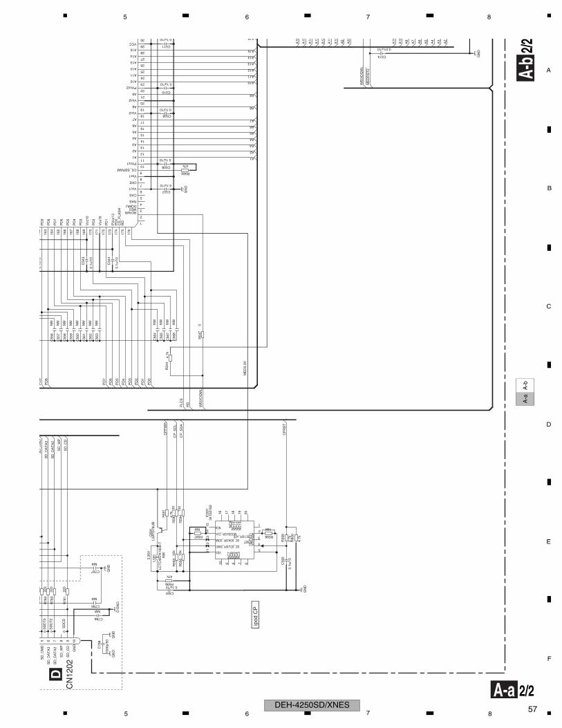
C
D
F
A
B
E
PD
9
PD
8
SD
_DA
TA
2
SD
_DA
TA
3
SD
_CM
D0.
1u/1
016
2P
D9
163
PD
816
4P
D7
165
5 6 7
R78
522
0
R78
422
0
R78
322
0
SD
DT
3
SD
DT
2C
556
NM
C55
7N
MS
D_D
AT
A2
SD
_CM
D
SD
_DA
TA
3
5 6 7 8
A-b
A-a
A-a 2/2
A-b
2/2
CP
_SD
A
CP
_SC
L
A7
A6
A5
A4
A3
A1
A9
A10
A11
A12
A13
A14
A15
A16
A8
CP
PW
R
RD
FLC
S
PD
5
PD
7
WE
0/D
QM
L
A9
A8
A6
A19
WE
0/D
QM
L
A15
A7
A4
A5
A2
A14
A12
A3
A13
A10
A16
A18
A20
A11
A2
CP
RS
T
PD
6
PD
4
PD
3
PD
2
PD
1
PD
0
ME
DR
ST
2
SD
_CD
SD
_WP
C59
2
0.1u
/10
C508
0.1u/10
C507
0.1u/10
C510
0.1u/10
C509
0.1u/10
C54
3
0.1u
/10
C54
4
0.1u
/10
C574
0.01u/10C511
0.1u/10
C591
0.1u/10
GN
D
GN
D
GN
D
GN
D
341S
2162
IC59
1
NC1
1
MODE1/SPI_nSS
2
NC2 3nRESET
4VCC
5
NC
3
6
NC
47
NC
58
NC
69
NC
7
10
VSS11
I2C_SCL/SPI_SIMO12
I2C_SDA/SPI_SOMI13
MODE0/SPI_CLK14
NC815 NC
9
16
NC
10
17
NC
1118
NC
1219
NC
13
20
RD/WR
1
WE0
2
DQMU3
RAS4
CAS5
Vcc16
CKE7
Vss18
CS_SDRAM9
PVcc110
A111
A212
A313
A414
A515
A616
A717
Vcc218
A819
Vss220
A921
PVcc222
A1023
A1124
A1225
A1326
A1427
A1528
29
30
PD
616
6P
D5
167
PD
416
8P
D3
169
Vcc
1017
0P
D2
171
Vss
1617
2P
D1
173
PV
cc13
174
PD
0
175
CS
_FLA
SH
176
RD
L591
LCT
C4R
7K16
08-T
LSA
1576
UB
Q59
1
R59
1
4.7k
R54
44.
7k
R60
0
4.7k
R54
70
R59
410
0
R59
210
0
R59
510
k
R59
310
k
R59
9
2.7k
R596
47k
R597
NM
R598
NM
C785
NM
GN
DC786
NM
8 9 10
R78
122
0S
DC
D
R560
47k
C55
8N
M
C55
9N
M
C56
0N
M
C56
1N
M
C56
2N
M
C56
3N
M
C56
4N
M
C56
5N
M
C56
7N
M
C56
8N
M
C787
NM
GN
D
C78
8
1000
p/50
GN
D
ipod
CP
VCC
SD
_CD
GN
D
SD
_WP
D
ME
D3.
3V
NM
3.26
V
DC
N12
02
DEH-4250SD/XNES 575 6 7 8

C
D
F
A
B
E
818
10k
1815
.8k
R18
54
10k
R18
58
NM
1120-A
1811
1
2
3
4
5
E1
652 1
C1
D1849-1
D o
1 2 3 4
10.3 KEYBOARD UNIT
B
DC
LK
DO
UT
RE
SE
T
XO
UT
VS
S
XIN
VC
C
MO
DE
RE
MX
RE
ST
DP
DT
KY
DT
MC
LK
AD
KE
Y2
VR
EF
AD
KE
Y1
AD
KE
Y0
XC
MD
OEL
R-IL
M
Grille MICRO
G_I
LM
C19
02
0.01
u/50
C18
9110
u/10
C19
01
0.1u
/16
C1921
1u/10
C19
23
1u/1
6
C1922
1u/10
D19
01
1SS
355
ILMGND
DGND
DGND
OELG
DGND
DGNDDGND
DGND
DGND
IC19
01P
EG
268-
A-K
1234567891011 12 13 14 15 16 17 18 19 20
IC18
91
GP
1UX
C14
RK
1R
EM
2G
ND
3V
CC
L190
1
NM
R19
24
100
21 436 58 7
R18
17
8.2k
R1
R1855
2.2k
R18
56
10k
R18
57
6.8k
R
1
R1904
47k
R1816
3.3k
R19
05
47k
R19
23
NM
R19
01
47k
R1891
120
R18
77
10k
R1893
2.2
R18
80
3.3k
R18
72
1.2k
R18
76
33k
R18
82
33k
R18
92
NM
R19
09
1k
R19
03
47k
R19
22
51k
R19
06
47k
R18
59 0
R19
08
10k
R19
07
47k
R18
71
10k
R18
78
1.2k
R19
02
150k
R18
79
1.8k
R18
81
8.2k
R18
74
3.3k
R18
75
8.2k
R18
73
1.8k
CSG1155-A
S1873
1
2
3
4
CSG1155-A
S1877
1
2
3
4
CSG1155-A
S1878
1
2
3
4
CSG1155-A
S1879
1
2
3
4
CSG1155-A
S1880
1
2
3
4
CSG1155-A
S1881
1
2
3
4
CSG1155-A
S1882
1
2
3
4
CSG1155-A
S1875
1
2
3
4
CSG1155-A
S1874
1
2
3
4
CSG1155-A
S1871
1
2
3
4
CSG1155-A
S1876
1
2
3
4
CSG1155-A
S1872
1
2
3
4
CSX
S
6GND
7C
8D
9Push
10Phase_B
DPDT
MO
DE
VC
C
VSS
RESET
KYDT
X1901CSS1577-A
11
22
33
CKS6036-ACN1921
123456789101112131415
R19
25
100
21 436 58 7
ILMGND
Q18
31IM
X9
B1
C2
4E
23
B2
LTC114EUBQ1832
R1867
5.6k
R19
10
47k
L192
1
NM
L1922
NM
R1894
NM
2
0.16 0.54BAND
over~under0.00 016
ADKEY1 SW(V)
DISP
1.00 1.590.54 1.00CLK
1.59 2.31
2.31 3.163.16 3.30
S.Rtrv
1
6
10.000MHz
(1.2
5MH
z)
YF
106
LIST345
EJECT
VS
SD
2
SO
_TX
SI_
RX
SC
L
XC
MD
XR
ES
XC
S
VD
D
VS
SD
1
XI
VS
SA
VA
H
VK
H
IRE
F
VS
SK
ADKEY2
RELEASE RELEASE
BAND
DISP
CLK
1
2
6
S.Rtrv
LIST
3
4
5
EJECT
REDGREEN
A,B,C
A:DEH-4250SD/XNESB:DEH-4250SD/XNES1C:DEH-4290SD/XNIDD:DEH-3200UB/XNUC
3.29V
9.06V
OEL MODULE
B KEYBOARD UNIT
DEH-4250SD/XNES581 2 3 4

C
D
F
A
B
E
ILMG
R1855
2.2k
1
6GND
7C
8D
9Push
10Phase_B
LMGND
Q18
31IM
X9
E2
B
EDGREEN
5 6 7 8
B
ROTARY COMMANDER
CKS6049-ACN1801
1
2
3
4
5
6
7
8
9
10
11
12
13
14
15
16
17
18
19
20
C18
46C
1845
C18
44C
1843
C18
42
C18
41C
1840
C18
39
C18
38C
1837
C18
36
C18
47 C18
34C
1833
C18
32
C18
48
NM
C1804
100p/50
C1805
1000p/50
C1806
1u/6.3
C18
03
4700
p/50
C18
02
4700
p/50
C18
35
C18
01
0.1u
/16
D18
36D
1837
D18
35
D18
39
D18
63
D18
54
D18
42
D18
45
D18
51D
1849
D18
50
D18
44
D18
33
D18
31
D18
41
D18
38
D18
43
D18
40
NM
D18
66
D18
47D
1846
D18
53
D18
61
D18
52
D18
62
D18
65
D18
60
D18
57
D18
59D
1858
D18
34
D18
56D
1855
D18
05
DA
P20
2U
D18
04
DA
N20
2U
D18
02
NM
D18
03
NM
OELG
DGNDND
DGND
DGND
ILMGND
DGND
JA1801YKN5006-A
21
3
L180
1
NM
11
22
33
44
NMQ1833
R18
49
R18
13
10k
R18
19
NM
R1818
10k
R1815
1.8k
R18
51
R18
40
R18
38
R18
37
R18
31
R1802
NM
R18
41
R18
43
R1801
NM
R18
54
10k
R18
44
R1812
1kR1811
1k
R18
61
NM
R18
14
1.2k
R18
60
NM
R18
42
R1804
2.2kR1805
2.2k
R18
58
NM
R18
03
NM
R18
39
CSG1155-A
S1801
1
2
3
4
CSX1120-A
S1811
Phase_A1
Enc_Com2
A3
B4
5 Com
VA
1802
NM
VA
1801
NM
R18
45
R18
35
R18
62
R18
63
R18
64
R18
65
R18
66C1807
NM
E1
6
B1
5
C2
43 2
B2
1C
1
DGND
DGND
CN1802YKS5036-A
1
2
3
4
5
6
C18
08
1u/6
.3
R19
41
R19
49
R19
48
R19
47
R19
42
R19
43
R19
44
R19
45
R19
46
SRC
DGND
ILMG
ILM+B
ROT1
DPDT
VBUS(US5V)
OEL+B
GREEN
AUXG
RED
D+
AUXR
SW3.3V
USBG
SOURCE
DSEN
USBG
AUXL
KYDT
D-
OELG
B(LEFT)A(UP)
D
RELEASE
PUSH
over~underJOYST(V)
C(DOWN)D(RIGHT)
PUSH
C
A
B
SW
ROT0
1801 1810
1811 1820
1831 1870
1871 1890
1891 1900
1901 1910
1921 1940
AUX & USB
ROTARY COMMANDER
LED
BUTTON
to REM
Grille MICRO
OEL
REFERENCE AREA MAP
0.16 0.54
1.59 2.312.31 3.163.16 3.30
1.00 1.590.54 1.00
0.00 0.16
RELEASE
D1831-1846 : CL-195SR-CDD1849-1862,1865 : CL-195PG-CD
1/4W
1/4W
1/4W
1/4W
1/4W
1/10
W
1/10
W
1/10
W
1/10
W
1/10
W
1/10
W
1/4W
1/4W
1/4W
1/4W
1/4W
1/4W
1/10
W
1/4W
1/4W
1/4W
1/10
W
1/10
W
1/10
W
1/10
W
1/10
W
1/10
W
1941 1949 LED
D only
270
560
NM
NM
NM
NM
NM
NM
NM
NM
NM
NM
NM
NM
NM
NM
NM
NM
NM
NM
150
330
NM
NMNM
NM
NM 33
0
330
330
220
470 15
0 150 15
0
470
470
470
470
18027
0
390
470
3.29V
14.16V
14.16V
CN801
1/2A
USB
AUXAUX:+2.20 dBs
DEH-4250SD/XNES 595 6 7 8

C
D
F
A
B
E
RE
SE
T
C21
5
RS
T
INT
Q
3C
VD
D4
5IC
EC
K6
SO
7S
CK
8S
I
15
9k
R21
4
10k
C21
3
3300
p/50
PD
2
/RS
T3
INT
Q(I
NT
1)4 5
71A
D.V
dd72
EF
M73
AS
Y74
1 2 3 4
10.4 CD CORE UNIT(S11STD-DOUT)
C
C101 C102 C110 C111C204 C207 C235 C239
C301 C307 C308
C701 C702 C703 C705 C707 C708D101
TH201Q201
C240 C281 C282 C283 C284
C601 C602
R106R297 R246R603 R604R710 R711
R281 R282 R283 R291 R292 R293 R299
R601 R602 R606
R225 R722
R242 R243 R707 R721 R723
C205 C206
CN702
FOP
FOM
TOM
TOP
TD
FD
SO
M
SO
P
LCO
M
LCO
P
LOE
J
TOM
FOM
FOP
TOP
E
BD
SD
CO
NT
SOM
SOP
LCOM
LCOP
HOME
8SNS
DSCSNS
MD
LD
PD
LD
CLC
ON
T
BD
F
E
AC
AC
PD
F
V+3A
REFO
PUEN
IC301BA5839FP
VR1
OPIN2+2
OPIN2-3
OPOUT24
5 OPIN1+
6 OPIN1-
7 OPOUT1
29FIN1
9MUTE
10 PowVcc1
11VO1-
12VO1+
13VO2-
14VO2+
8GND1
15VO3+
17VO4+
18VO4-
19PowVcc2
20GND2
21CNT
22LDIN
23OPOUTSL
24OPINSL
25OPOUT3
26OPIN3-
27OPIN3+
28PreVcc
16VO3-
30FIN2
SIN
CIN
TIN
FINCSN1067-A
S901
1
234
CSN1068-A
S905
1
234
HOME
8SNS
DSCSNS
BLK
RED
PL
OG
NMC
301
MDYMDX
LOEJ
CONT
D10
1
NM
TO
P
FO
P
TO
M
FO
M
R10
1
2.4
R10
2
2.4
R10
3
2.7
LD
LD1
C10
4
4.7u
/6.3
(212
5)
ADCIN
FE
TE
TEC
RFO
RFAGC
ATEST
V+3A
PD
CLCONT
M2 LOAD/CRG MOTORCXC4026
M1 SPDL MOTORCXE2273
FOCUS ACT1
TOP2
FOP3
FOM4
TOM5
MD6
A+C7
VR8
VREF9
P1+P610
GND11
P5+P1012
VCC13
B+D14
LD+15
LD-
VC
C
TRK ACTC
101
NM
C10
2
NM
C221
0.1u/10
C220
0.1u/10 C219
0.1u/10
C222
0.1u/10
C225
0.01u/16
C217
56p/50
C223
68p/50
C224
47p/50
C216
1800p/50
C30
4 4700p/25
C30
5 0.022u/16
R10
8
1M
R106
NM
R30
5
18k
R306
18k
R30
7
18k
R308
18k
R21
8
4.7k
R216
1.2k
R21
7
5.6k
2SA1577(QR)
Q101
EFBD
AC
ASY
EFM
CSN1068-A
S903
1
234
REFO1
REFO2
C307
NM(1608)
CN702CKS5766-A
1V
DD
2
C229
0.1u/10
C236
0.1u/10
C306
1u/10(1608)
C11
0
NM
C21
8
4p/5
0
C11
1
NM
V3R3
CKS4808-ACN101
1
2
3
4
5
6
7
8
9
10
11
12
13
14
15
R109
2.2k
C23
9
NM
NMC
308
UNR511MGQ102
C21
4
0.04
7u/1
0
R2
3
LD1
AT
ES
T75
A.Vdd176
A.GND177
RFI78
AGCO79
C3T80
AGCI81
RFO82
EQ283
EQ184
RF2-85
RF-86
A.GND287
A.Vdd288
A89
B90
F91
E92
REFOUT93
FE-94
FEO95
ADCIN96
TE-97
TEO98
TE299
TEC100
C228
27p/50
R229
470
E:P5+P10F:P1+P6
HOLOGRAM UNIT
PICKUP UNIT(P10.5)(SERVICE)CXX1942
F.ACT: Applying positive voltage to FOP, the lens approaches DISC.
T.ACT: Applying positive voltage to TOP, the lens moves outer circumference of DISC.
CLCONT
MOTOR DRIVER LOGIC TABLE
LOEJ
CONT
LOAD EJ PLAY OFF
HH L L
-
L
-
H
L
L
H
L
VDD
GND
PGND
VD
REFO
REFO
RE
FO
*
(1/1
0SR
,160
8)
*
*
**
*
* *
*
*
A
D
I
P
C209 C238 C240C306 C307
R243 R246R101 R102 R103
C104
1608:PARTS
2125:PARTS
R606
Parts with Polarity
IC201 IC301D101Q101 Q102 Q201
C205 C301 C308
*
D
A
I
P
*
CIRCUIT No.
(1/1
0W)
C708
Digital Out model only
Analog Out model only
IIC-BUS model only
P-BUS model only
HOME
8EJ
DSCSNS
SWITCHES:CD CORE UNIT S901:HOME SWITCH.........ON-OFF S903:DSCSNS SWITCH.....ON-OFF S905:8EJ SWITCH..............ON-OFF
The underlined indicates the switch position.
F
T
T
F
F
T
T
F
F
T
T
F
F
T
F
T
F
T
C
C
S
S
S
C
C
S
C
S
1
2
3
9
a
7
84
5
f
c
d
e
DEH-4250SD/XNES601 2 3 4

C
D
F
A
B
E
ATEST
ASY
EFM
CN70CKS5766-
NM
A.Vdd176
A.GND177
RFI78
AGCO79
C3T80
AGCI81
RFO82
EQ283
EQ184
RF2-85
RF-86
A.GND287
A.Vdd288
A89
B90
F91
E92
REFOU93
FE-94
FEO95
ADCIN96
TE-97
TEO98
TE299
TEC00
BLE
OFF
L
-
L
*
5 6 7 8
C
P
A A
A
D
I
P P
A
A
P
I
D
D
D
D
D
D
P
SCL
MD
SD
LOEJ
SK
IP
/CD
SR
Q
AD
EN
A
CLCONT
TE
MP
VD
SE
NS
CONT
RESET
ADENA
TEMP
/CDSTBY
/WAIT
VPP
ICECK
DSCSNS
8SNS
SC
K
ICE
CK
SC
K
FD
HOME
TD
BCLK
LRCK
DATA
SDA
VP
P
PU
EN
CVDD
CV
DD
SKIP
/CDSRQ
VDSENS
/CDSTBY
RE
SE
T
/WA
IT
LRCK
DATA
SCL
SDA
DATA
/WAIT
BCLK
LRCK
BCLK
RESET
VDD
VD
PGND
GN
D
CD
SR
Q
CD
ST
BY
SC
L
SK
IP
SD
A
RE
SE
T
LRC
K
BC
LK
DA
TA
X201CSS1603-A
1
2
3
PUEN
TESTIN
R24
6
NM
(160
8)
VDSENS
TEMP
C20
30.
1u/1
0
C207
NM
C210
0.1u/10
C211
0.1u/10
C21
2
0.1u
/10
C21
5
0.1u
/10
C206
NM
C23
5
NM
C71
010
00p/
50
C232
1000p/50
C231
1000p/50
R264
1k
R254
100k
R253
100k
R26
0
10k
R23
5
10k
R23
6
10k
R263
4.7k
R262
4.7k
NMTH201
NMQ201
RS
T
INT
Q A0
ST
B
SC
K
SO
SI
ICE
MD
VP
P
CV
DD
ICECK
C16
M
MO
NI0
MO
NI1
MO
NI2
VD
2
VD
1V
DD
1
GN
D1
GN
D2
GN
D3
R242
NM
R245 100k
C233
0.01u/16
R237
220
R240
47k
C70
5
NM
VD
D2
2A
1V
DD
2
3C
VD
D4
5IC
EC
K6
SO
7S
CK
8S
I
9V
PP
10G
ND
R29
6
0
C20
4N
M
C70
7
NM
C70
2
NM
C209
0.1u/16 (1608)
C23
8N
M(1
608)
C24
0N
M(1
608)
C70
8
NM
(160
8)
R283
0 C281
NM
C282
NM
NM
C205
R29
4
470
C70
1
NMC70
3
NM
WA
IT
C283
NM
C284
NM
R243
NM(1608)
PG
ND
1
PG
ND
2
ADENA
C29
9N
M
R706
220R702
100
R701
100
R297
NM
C601
NM
C602
NM
R723
NM
R721
NM
R70
7
NM
R606
NM (1608)
R722
0
R709
0
R708
0
R29
9
0
C21
4
0.04
7u/1
0
R215
39k
R21
4
10k
C21
3
3300
p/50
CKS6146-ACN701
1 VD
2 VD
3 /CDSRQ
4 /CDSTBY
5 SCL
6 SKIP
7 SDA
8 RESET
9 VDD
10 GND
11 DATA
12 BCLK
13 LRCK
14 GND
15 PGND
16 WAIT
AAGND1 AAGND2
R225
0
R292 0
R293
0
R71
0
NM
R71
1
NM
IC201
PE5706A
LD1
PD
2
/RS
T3
INT
Q(I
NT
1)4
A0
5
/ST
B6
/SC
K7
SO
8
SI
9
D.V
dd10
D.G
ND
11
RE
G16
12
RE
GS
13
DA
.Vdd
114
RO
UT
15
DA
.GN
D1
16
RE
GC
17
DA
.GN
D18
LOU
T19
DA
.Vdd
20
ICE
MD
21
X.V
dd22
/XT
AL
23
X.G
ND
24
XT
AL
25
Vpp26
C.Vdd27
C.GND28
RESET29
IO.GND130
IO.Vdd131
ICECK32
/CDSTBY33
34HOME
3512SNS
368SNS
37DSCSNS
38CONT
39CLCONT
40LOEJ
41PA7
42DOUT
43SCKO
44LRCK
45TX/EMPH
46/WAIT
47SCL
48SDA
49PC3
50
/TE
ST
IN51
/CD
SR
Q52
SK
IP5354
/AD
EN
A555657
TE
MP
58M
onito
r059
Mon
itor1
60M
onito
r261
Mon
itor3
62S
D2
63IO
.GN
D2
64IO
.Vdd
265
FD
66T
D67
SD
68M
D69
TE
ST
70A
D.G
ND
71A
D.V
dd72
EF
M73
AS
Y74
AT
ES
T75
T
R232
0
BS
CK
0
LRC
K0
EJSW
R60
1
NM
R60
2
NM
R603
NM
R604
NM
R281 56
R282
56
R291
56
NO MOUNT PARTS (NM)*
Land for manual soldering
GND
GND
GND
3.3V
7.5V
7.5V
I/O
VDD
GND
GND
EJSW
VD
CO
NT
VD
SE
NS
*
*
*
*
*
*
*
**
*
*
*
*
*
*
*
(RO
UT
)
(LO
UT
)
(AG
ND
)
*
**
R294MaskFlash
4700
MaskR232
Flash 10k0
PU
EN
* *
* *
*
Mask FlashR281R282R291
565656
22
2222
ACN701
C CD CORE UNIT(S11STD-DOUT)
FSIGNAL LINEFOCUS SERVO LINETRACKING SERVO LINECARRIAGE SERVO LINESPINDLE SERVO LINE
T
C
S
S T FC
6
i h g
b
DEH-4250SD/XNES 615 6 7 8

C
D
F
A
B
E
1 2 3 4
10.5 SD UNIT
D
VKN1302-ACN1202
1GND
2
3
4
5
6
7
8
9
10
CKS6180-A
CN1203
1C
D/D
AT
3
3V
SS
1
5C
LK
7D
AT
0
9D
AT
2
11G
ND
2
13CD/WP
14WP
12CD
10G
ND
1
8D
AT
1
6V
SS
2
4V
DD
2C
MD
15NC1
16NC2
17GND3
18GND4
19GND5
20GND6
SD_CD
SD_WP
SD_DATA2
SD_CMD
SD33V
SD_CLK
SD_DATA3
SD_DATA1
SD_DATA0
3.29V
D SD UNIT (A,B,C only)
CN781
2/2A
A:DEH-4250SD/XNESB:DEH-4250SD/XNES1C:DEH-4290SD/XNIDD:DEH-3200UB/XNUC
DEH-4250SD/XNES621 2 3 4

C
D
F
A
B
E
5 6 7 8
10.6 WAVEFORMS
- Waveforms Note : 1. The encircled numbers denote measuring points in the circuit diagram.2. Reference voltage REFO1(1.65 V)
500 ms/div5 V/div5 V/div5 V/div10 V/div
1DSCSNS5CLCONT4LOEJ6VD
5 V/div5 V/div5 V/div5 V/div
1DSCSNS28SNS4LOEJ3HOME
5 V/div5 V/div5 V/div5 V/div
500 ms/div1DSCSNS28SNS4LOEJ3HOME
500 mV/div500 mV/div
200 ms/divcTEdFE
200 mV/div2 V/div2 V/div
500 ms/divaFINbRFOK(MONI_3)7SIN
1 V/div500 mV/div500 mV/div
2 s/div
500 ms/div
7SIN8CIN9TIN
2 V/div500 mV/div
5 μs/diveMDX7SIN
2 V/div500 mV/div
50 ms/diveMDX7SIN
500 mV/div500 mV/div500 mV/div500 mV/div
20 ms/divdFEaFINcTE9TIN
1 V/div500 mV/div500 mV/div
500 μs/divfRFAGCcTE9TIN
500 mV/div500 mV/div
2 ms/div cTEfRFAGC
500 mV/div500 mV/div
200 ms/divaFINdFE
Source On setup operation12 cm CD-DA Source On setup operation
CD-DA Play operation Spindle waveform during play operation Spindle waveform during play operation(Wider)
Focus Search waveform Track Open waveform 100 Track Jump waveform (32 Track Jump x 3)
12 cm CD-DA setup operation after loading
12 cm CD Loading operation 12 cm CD Loading operation 8 cm CD Loading operation
Ref.:GND
Mode:Normal
Ref.:GND
Mode:Normal
Ref.:GND
Mode:Normal
Ref.:REFO
Mode:Normal
Ref.:REFO
Mode:Normal
Ref.:REFO
Mode:Normal
Ref.:REFO
Mode:TEST
Ref.:REFO
Mode:TEST
Ref.:REFO
Mode:TEST
Ref.:REFO
Mode:Normal
Ref.:REFO
Mode:Normal
Ref.:REFO
Mode:Normal
DEH-4250SD/XNES 635 6 7 8

C
D
F
A
B
E
1 2 3 4
2 V/div2 V/div2 V/div
10 μs/divgLRCKhBCLKiDATA
1 V/div1 V/div500 mV/div2 V/div
200 ms/divfRFAGCcTE8CIN7SIN
1 V/div500 mV/div500 mV/div
2 ms/divfRFAGCcTE9TIN
5 V/div5 V/div5 V/div5 V/div
500 ms/div1DSCSNS28SNS4LOEJ3HOME
5 V/div5 V/div5 V/div5 V/div
500 ms/div1DSCSNS28SNS4LOEJ3HOME
5 V/div5 V/div5 V/div
500 ms/div1DSCSNS5CLCONT4LOEJ
1 V/div1 V/div1 V/div1 V/div
500 μs/divfRFAGC9TINcTEaFIN
12 cm CD Eject operation8 cm CD Eject operation
Black Dot (800 μm) during play
12 cm CD Eject operation
32 Tracks Jump waveform (Zoom of 100 Track Jump waveform) Search operation(Outter to Inner) Digital Out waveform
Ref.:REFO
Mode:TEST
Ref.:GND
Mode:Normal
Ref.:REFO
Mode:Normal
Ref.:REFO
Mode:Normal
Ref.:REFO
Mode:Normal
Ref.:GND
Mode:Normal
Ref.:AGND
Mode:Normal
DEH-4250SD/XNES641 2 3 4

C
D
F
A
B
E
5 6 7 8
DEH-4250SD/XNES 655 6 7 8

C
D
F
A
B
E
1
5
10
15
2
0
1
5
1
C201
IC1
C202
C203
C201
C35
2C
356
C365
C368
R794
C188
781
R2
8
CN
FRO
C C
1 2 3 4
11. PCB CONNECTION DIAGRAM11.1 TUNER AMP UNIT
A
A TUNER AMP UNIT
CapacitorConnector
P.C.Board Chip PartSIDE B
SIDE A
NOTE FOR PCB DIAGRAMS1.The parts mounted on this PCB include all necessary parts for several destination. For further information for respective destinations, be sure to check with the schematic dia- gram.2.Viewpoint of PCB diagrams
1
15
2530
3540
1
E E 1
1
1
1
5
E
E
1
1
EE
1
15
10
1 1 1
IC151
D751
IC161
D383
D581
D583
P301
IC581
VA661
IC582
VA662
IC583
R661R662
JA661
Q301 Q302 Q303
I
Q901
Q902
L151
Q361
R301
Q362
R302
Q363R303 R304R305 R306
R307 R308
L161
Q751
R309
Q752
R310R311R312
R313
R314
R31
5 R31
6
JA301
Q382
R901
R902
R911
R912
Q781Q782
C301
C302C303
C304
C305
C306
C307 C308C309
C310C311
C312
R161R162
R163
R36
1
C901
R362
C902
R36
3
C903
R36
4
C904
R36
5R
366
R751R752
R753 R754
C911
C912
C913
C151
C152
R385
R581
C161 C162
C163
C164
C165
C166
R789
C36
7
C369
C751
C752
C753
R790
C754
C381
D902
C582
C583
C584
C585
C586C587
C588
C
D161
IC911
D162
D163D164
R201
R205
10 20 30 40 50 60 70X
150
140
130
120
110
100
90
80
70
60
50
40
30
20
10
0
Y
D
RCA
WIRED REMOTE
DEH-4250SD/XNES661 2 3 4

C
D
F
A
B
E
2530
3540
1
E
12
Q363
QQ782
R36
5R
366
R789
C36
R
R201
R205
70
5 6 7 8
A
SIDE A
1
1 10
15101520
25 30 35 40 45
1 5
10
15
20
1
5
10
15
2
0
1 510 15 20 25
30 35 40 45 50
55
60
6
5
70
7
5
80 85 90 95 100
1
E
E
1
5
E
1
1
5
10
15
2
0
25
3
0
35
40
45 50 55 60 65 70 75 80 85
90 95 100 105 110 115 120 125 130
135 140 145 150 155 160 165 170 175
E
E1
E
E 1
5
1
1
1
1
1
E
E
10
1
5
10
15
E
1551
10
15
1015
20
1 515
0201
1
1
1
10
1
5
1
510
52515
2010
1
1
D941
R401
D942
R402R403R404
VA811
R405R406R407R408
R409
R600
IC351
L841
R601
R60
3
R604
D951
R605R606
R607
R608
R609
R80
1
R80
2
R80
3
R610
R80
4
R80
5
R61
3R
614
R80
8
R61
5
JA401
R61
6
R61
7R
618
R61
9
R81
0
R81
1
CN601
R812R813
R81
4
R62
0
R62
1
R81
6
R622
R623
R62
4
IC181
C201
IC182
R626C202
R627
C203 R628
R62
9
CN801
R82
1
C209
IC571
R82
2
R823
R630
R63
1
C401
R63
2
C402
C403
C210
C404
D981
C405
D982
C406
C407
C408
C214
C215
C217
C218
R831
C601
R832
C602
R833
C603
R834
C604
R641
C605
R642
C606R643
C607
C608
C609
C610
X601
IC591
R841
R842R843
R84
4
R651R652
C831
C832
C641
C841
C842
C651
BZ601
D601
D602
IC201D
801
L501
D80
2
L502
D80
3D
804
D80
5
S651
L701
IC601
Q921
D831
Q931
D651
R50
1
R502
R50
4R
505
Q181
Q951
IC641
R50
9
Q182
R701
R702
R703
R51
0
R704
R51
1
R705
R51
2
R706
R51
3
R707
R708
R709
R518
IC651
R51
9
R710
L181
L951
R711R712R713
R714
U401
R521
R71
5
R522
R716
R717
R524
L571
CN701
R529
781Q783
R530
Q591
R151
R921
R922
R923
R924
R925
C501
KN401
R926
C502
C50
3
C504
L781
C505
C50
6
C507
R54
4
C508
L591
C509
R54
7
R93
1
C701
R932
C702
C703
C510
C704
L981
X501
C511
C705 C70
6
C512
X503
C513
C514
R551
C515
R55
2
C51
6
R55
3R554
C519R557
R55
8
R55
9
C520
C521
C522
C523 C524R561
C52
5
C526
C52
7
C52
8
C52
9
R181
R951
R182
R95
2
R18
3R
184
R95
4
C53
0
R185
C531
C532
C533C534
R57
2 R573
C537
R574
C538
R575
C539
C921
R576
R577
R38
3
R578
R191R192
C540
C541
C542C543
C544
C35
1
C545
C54
6
C35
2
C35
3
C548
C35
4
C549
C35
5
C93
1
C35
6
C932
C35
7
C35
8
R781
C55
2C
553
R783
C55
4
R784
C55
5
R591
R785
C361
C55
6
R592
R786
C55
7R59
3
R787
C36
3
C55
8
R594
R788
C36
4
C55
9
R595
C365
C941
Q401
R596
Q402
R597
C368
R598
9
R59
9
C56
0
790
C56
1
L201
C56
2
R79
2
C56
3
R793
C564
R794
C56
5
R795
R796
C56
7C
568
C181
C951
C182
C183
C184
CN781
C185
L401
C186
L402
L403
C187C188
C189
C57
1
C57
2
C574
C190
C19
1
L601
C192
L602
C193
L603
C194
JA981
C195
C196
IC501
L801
C781
C785
C591
Q821
C786
Q822
C592
C787
D921
D922Q832
D931
VA
801
R202
VA802
R203
VA
803
Q841
Q842
R206
VA
806
R20
7
VA
807
R20
8
VA
808
80 90 100 110 120 130 140 150 160 170
FUSE
D CN1202
FRONT
FM
/AM
TU
NE
R U
NIT
ANTENNA
CORD ASSY
B CN1801
RESET
C CN701
DEH-4250SD/XNES 675 6 7 8

C
D
F
A
B
E
90
E
Q831
1 2 3 4
A
A TUNER AMP UNIT
170 160 150 140 130 120 110 100
1
R602
R809
C801
C802
C431
C432
C433
ZNR401
D431
IC431
R514
R515
R525
R526
R527
R531
R532
R533
R534
R535R560
C535
C536
C547
C550
C551
C362C366
L404
C788
D432
1
10
1
1
1
1
DEH-4250SD/XNES681 2 3 4

C
D
F
A
B
E
100
C362
C788
1
1
5 6 7 8
A
SIDE B
90 80 70 60 50 40 30 X
150
140
130
120
110
100
90
80
70
60
50
40
30
20
10
0
Y
20 10
E
E
1
D381 D382
D582
C211
C212
C213
C216
C219
C220
C221C222
Q381
R164
R166
R167
R168
R169
C905C906
C907
R381R382
R384
C167
D901
D903
C581
IC901
Q831
R165
10
1
DEH-4250SD/XNES 695 6 7 8
C
D
F
A
B
E
1 2 3 4
11.2 KEYBOARD UNIT
B
SIDE AB KEYBOARD UNIT
E
1
1
1
1
1
1
1
1
1
1
1
1
1
1
1
5
10
1 5 10 15
15
1
CN
1921
C19
21
C19
22
R19
06R19
07
R19
22
R19
24
CN
1802
C18
32
C18
33
C18
34
C18
35
JA18
01C
1836
C18
37
Q18
33
C18
38
C1839
C1840
C18
41
C1842
C1843
C1844C
1845
C18
46
C18
47
C18
48
S18
01D
1831
D18
33
D18
34D
1835
73
81
D6
38
1D
D18
38
D1839
S18
11
D1840
D18
41
D1842
D1843
D1844
D18
45
D18
46
D18
47
D18
49
L192
2
D18
50
D18
51
D18
52D
1853
D18
54
D1855
D1856
D18
57
D1858
D1859
D1860
D18
61
D18
62
D18
63
R18
60
D18
65
R18
61
R18
71R
1872
R18
73R
1874
R18
75
R18
76
R18
77
R18
78R
1879
R18
80
R18
81R
1882
R18
94
S18
71S
1872
S18
73
S18
74
IC18
91
S18
75S
1876
S18
77S
1878
S18
79S
1880
S18
81
S18
82
D1866
1020
3040
5060
7080
9010
011
012
013
014
015
0X
40 30 20 10
0
Y
160
US
B
AU
X
EJE
CT
65
43
21
CLK
DIS
P
LIS
TR
OT
AR
Y C
OM
MA
ND
ER
S.R
trv
BA
ND
SR
CC
EL
MO
DU
LE
DEH-4250SD/XNES701 2 3 4

C
D
F
A
B
E
5 6 7 8
B
SIDE BB KEYBOARD UNIT
160150
140130
120110
10090
8070
6050
4030
20
X
403020100Y
10
5
1
E
1
5
10
1520
1
1
5 15
1
2010
C1901
C1902
C1923
D1901
R1901
R1902
R1903
R1904
R1905
R1908
R1909
IC1901
R1910
L1801
R1923
R1925
R1941
R1942
R1943
R1944
R1945
R1946
R1947
R1948
R1949
VA
1801
VA
1802
CN
1801
C1801
C1802
C1803
C1804C
1805
C1806
C1807
C1808
X1901
D1802
D1803
D1804
D1805
R1801
R1802
R1803
R1804
R1805
Q1831
Q1832
R1811
R1812
R1813
R1814
R1815
R1816
R1817
R1818
R1819
L1901
R1831
R1835
R1837
R1838
R1839
R1840
R1841
R1842
R1843
R1844
R1845
L1921
R1849
R1851
R1854
R1855
R1856
R1857
R1858
R1859
R1862
R1863
R1864
R1865
R1866
R1867
C1891
R1891
R1892
R1893
AC
N801
DEH-4250SD/XNES 715 6 7 8
C
D
F
A
B
E
1 2 3 4
11.3 CD CORE UNIT(S11STD-DOUT)
C
SIDE AC CD CORE UNIT (S11STD-DOUT)
1 510 15 20 25
30 35 40 45 50
55
60
6
5
70
75
80 85 90 95 100
1 5 10 15
1 5 10 15
1 5
10
1
0151
152025
29
30
1
R214
R215
R216
R21
7
R21
8
R225
R229
R232
R23
5
R23
6
C203
C204
TH201
C207
C209
R246
C210
X201
C211
C212
C213
C214
C215
C216C21
7
C21
8
C219 C221C222C223
C224
C225
R26
2
R26
3
C22
8
R264
C235
C238
C240
R281
R282
R294
IC201C299 R305
R306
R307
R308
CN101
R707
R708
R709
R710
C102
CN701
CN702
C304C305
C306
C307
C701
C702
S901
D101
IC301
10 20 30 40 50 60 70X
60
50
40
30
20
10
0
Y A CN701
PICKUP UNIT(P10.5)(SERVICE)
F
E REFO1 M1SPINDLEMOTOR
M2LOADING/CARRIAGE
MOTORHOME
DEH-4250SD/XNES721 2 3 4
C
D
F
A
B
E
5 6 7 8
C
SIDE BC CD CORE UNIT (S11STD-DOUT)
70 60 50 40 30 20 10X
60
50
40
30
20
10
0
Y
E
E
1
1
E
R601
R602
R603
R604R606
R237
R240
C205
C206
R242
R243
R245
R253R254
C601
C602
C220
R260
C229
C231
C232
C233
C236
C239
R283
R291R292
R293
Q101
Q102
R296
R297
R299
C281
C282
C283
C284
R101
R102
R103
R106
R108
R109
R701
R702
R706
R711
C101
C104
R721R722
R723
C301
C110C111
C308
C703 C705
C707
C708
C710
S903
S905
Q201
8EJ
DSCSNS
DEH-4250SD/XNES 735 6 7 8

C
D
F
A
B
E
1 2 3 4
11.4 SD UNIT
D
SIDE AD SD UNIT
SIDE BD SD UNIT
1 5 10
1 015
15
20
CN1202
CN1203
10 20 30 40X
40
30
20
10
0
Y
10 20 30 40X
10
20
30
40
0
Y
A CN781
DEH-4250SD/XNES741 2 3 4

C
D
F
A
B
E
5 6 7 8
12. ELECTRICAL PARTS LISTNOTE: Parts whose parts numbers are omitted are subject to being not supplied. The part numbers shown below indicate chip components. Chip Resistor RS1/_S___J,RS1/__S___J Chip Capacitor (except for CQS.....) CKS....., CCS....., CSZS..... The > mark found on some component parts indicates the importance of the safety factor of the part. Therefore, when replacing, be sure to use parts of identical designation. Meaning of the figures and others in the parentheses in the parts list. Example) IC 301 is on the point (face A, 91 of x-axis, and 111 of y-axis) of the corresponding PC board. IC 301 (A, 91, 111) IC NJM2068V
Circuit Symbol and No. Part No.
A:DEH-4250SD/XNES
B:DEH-4250SD/XNES1
C:DEH-4290SD/XNID
D:DEH-3200UB/XNUC
Unit Number : CWN4805(A,B,C)
Unit Number : CWN5219(D)
Unit Name : Tuner Amp Unit
Unit Number : CWN4813(A,B,C)
Unit Name : Keyboard Unit
Unit Number : CWN5220(D)
Unit Name : Keyboard Unit
Unit Number : CWX3774
Unit Name : CD Core Unit(S11STD-DOUT)
Unit Number : CWN4816(A,B,C)
Unit Name : SD Unit
AUnit Number : CWN4805(A,B,C)Unit Number : CWN5219(D)Unit Name : Tuner Amp Unit
MISCELLANEOUS
IC 151 (A,62,91) IC R5523N001BIC 161 (A,50,102) Regulator IC BD9781HFPIC 181 (A,108,75) IC WM8761GEDIC 182 (A,80,99) IC NJM2872F05IC 201 (A,75,118) IC PM9012A
IC 351 (A,83,142) IC PA2030AIC 431 (B,152,131) IC NJM2885DL1-33IC 501 (A,121,50) IC R5S7262ZD144FPUIC 571 (A,148,51) Software Unit CWW1967
IC 581 (A,24,80) IC S-1172B33-E6
IC 583 (A,24,89) IC BH12PB3WHFVIC 591 (A,102,23) IC 341S2162IC 601 (A,128,96) IC PEG640A8IC 651 (A,119,108) IC S-80827CNNB-B8MIC 901 (B,24,70) Regulator IC S-1132B33-U5
IC 911 (A,7,122) IC NJM2388F84Q 301 (A,14,126) Transistor UMH3NQ 303 (A,29,126) Transistor UMH3NQ 361 (A,57,131) Transistor LTC114EUBQ 363 (A,70,128) Transistor RT3T22M
Q 381 (B,55,131) Transistor 2SC4081Q 382 (A,45,129) Transistor RT3T22MQ 591 (A,108,25) Transistor LSA1576UBQ 751 (A,7,94) Transistor 2SD2396Q 752 (A,16,104) Transistor RT3T22M
Q 781 (A,72,92) Chip Transistor(A,B,C) 2SB1689Q 782 (A,70,92) Transistor(A,B,C) LTC114EUBQ 783 (A,106,95) Transistor(A,B,C) DTA123EUQ 821 (A,95,126) Transistor 2SA1036KQ 822 (A,96,121) Transistor LTC114EUB
Q 831 (B,93,118) Transistor 2SD1664Q 832 (A,91,122) Transistor RT3T22MQ 841 (A,94,16) Transistor LSA1576UBQ 842 (A,93,11) Transistor LTC114EUBQ 901 (A,7,71) Transistor 2SD2396
Q 902 (A,14,77) Transistor RT3T22MQ 921 (A,136,108) Transistor RT3CLLMD 161 (A,28,96) Diode CRG03D 162 (A,28,94) Diode CRG03
D 163 (A,36,94) Diode CMS02D 381 (B,61,131) Diode UDZS8R2(B)D 382 (B,47,126) Diode DAN202UD 383 (A,54,128) Diode 1SS352D 581 (A,19,79) Diode 1SS352
D 582 (B,23,80) Diode CRG03D 601 (A,122,85) Diode RB551V-30D 602 (A,128,107) Diode RB751S-40D 651 (A,118,105) Diode 1SS352D 751 (A,12,104) Diode HZU8R2(B1)
Circuit Symbol and No. Part No.
DEH-4250SD/XNES 755 6 7 8

C
D
F
A
B
E
1 2 3 4
D 801 (A,116,14) Diode DZ2S068CD 802 (A,119,14) Diode DZ2S068CD 803 (A,122,13) Diode DZ2S068CD 804 (A,123,13) Diode DZ2S068CD 805 (A,124,13) Diode DZ2S068C
D 831 (A,91,119) Diode HZU10(B1)D 901 (B,14,97) Diode CRG03D 902 (A,12,77) Diode UDZS5R6(B)D 921 (A,141,122) Diode HZU7L(C3)D 922 (A,139,122) Diode HZU7L(A1)
D 941 (A,100,129) Diode CRG03D 942 (A,105,125) Diode CRG03D 981 (A,139,130) Diode CRG03D 982 (A,139,128) Diode CRG03
ZNR401 (B,164,117) Surge Protector IMSA-6802-01Y900L 161 (A,44,92) Inductor CTH1253L 181 (A,102,80) Chip Ferrite Bead DTL1107L 401 (A,153,103) Chip Coil BTH1100L 402 (A,155,73) Chip Coil BTH1100
L 404 (B,167,103) Chip Coil BTH1104L 501 (A,98,74) Inductor VTL1145L 502 (A,98,79) Inductor CTF1410L 601 (A,109,89) Chip Coil BTH1103L 801 (A,117,17) Inductor CTF1713
L 981 (A,116,141) Choke Coil 600 uH CTH1445X 501 (A,124,69) Oscillator 48.000 MHz CSS1760X 503 (A,103,43) Oscillator 16.93 MHz CSS1794X 601 (A,114,97) Oscillator 20.000 MHz CSS1795
S 651 (A,134,10) Switch CSG1020P 301 (A,40,118) Poly Switch MINISMDC075F/24VA661 (A,53,135) Varistor VR105C5R0AAAVA662 (A,53,133) Varistor VR105C5R0AAAVA801 (A,106,15) Varistor VR105C5R0AAA
VA802 (A,115,16) Varistor VR105C5R0AAAVA803 (A,120,14) Varistor VR105C5R0AAAVA806 (A,110,15) Varistor VR105C5R0AAAVA807 (A,111,15) Varistor VR105C5R0AAAVA808 (A,127,14) Varistor VR105C5R0AAA
CN701 (A,96,39) Connector VKN1192CN781 (A,96,61) Connector(A,B,C) VKN1186CN801 (A,114,4) Connector CKS6188JA301 (A,25,138) Pin Jack YKB5011JA401 (A,169,129) Antenna Jack CKX1070
JA661 (A,47,139) Connector CKS4124JA981 (A,118,141) Plug CKM1586
FM/AM Tuner Unit CWE2098> Fuse(10 A) YEK5001
RESISTORS
R 151 (A,96,90) RS1/16SS104JR 161 (A,42,103) RS1/16SS1003FR 163 (A,42,98) RS1/16SS683JR 165 (B,48,97) RS1/10SR1003DR 166 (B,47,99) RS1/10SR2402D
R 167 (B,45,96) RS1/10SR333JR 168 (B,52,99) RS1/10SR471JR 169 (B,47,101) RS1/10SR121JR 181 (A,102,95) RS1/10SR0R0JR 191 (A,92,103) RS1/16SS821J
Circuit Symbol and No. Part No.R 192 (A,92,104) RS1/16SS821JR 201 (A,69,124) RAB4CQ102JR 202 (A,80,105) RS1/16SS331JR 207 (A,81,105) RS1/16SS223JR 208 (A,81,106) RS1/16SS223J
R 301 (A,12,128) RS1/16SS821JR 302 (A,18,126) RS1/16SS821JR 305 (A,27,128) RS1/16SS821JR 306 (A,32,128) RS1/16SS821JR 307 (A,12,129) RS1/16SS223J
R 308 (A,17,129) RS1/16SS223JR 311 (A,28,129) RS1/16SS223JR 312 (A,32,129) RS1/16SS223JR 315 (A,23,130) RS1/16SS0R0JR 316 (A,26,130) RS1/16SS0R0J
R 361 (A,59,132) RS1/16SS103JR 362 (A,57,129) RS1/16SS103JR 363 (A,60,132) RS1/16SS331JR 365 (A,69,131) RS1/16SS103JR 366 (A,70,131) RS1/16SS103J
R 381 (B,59,132) RS1/10SR473JR 382 (B,63,133) RS1/10SR104JR 383 (A,134,84) RS1/16SS473JR 384 (B,50,129) RS1/10SR473JR 385 (A,45,131) RS1/16SS102J
R 401 (A,156,92) RS1/16SS681JR 403 (A,156,94) RS1/16SS681JR 404 (A,156,95) RS1/16SS681JR 405 (A,156,96) RS1/16SS681JR 406 (A,156,97) RS1/16SS681J
R 407 (A,156,98) RS1/16SS681JR 408 (A,156,99) RS1/16SS152JR 501 (A,134,65) RS1/16SS473JR 502 (A,140,66) RS1/16SS101JR 504 (A,132,65) RS1/16SS473J
R 505 (A,131,65) RS1/16SS473JR 509 (A,130,65) RS1/16SS473JR 510 (A,129,65) RS1/16SS473JR 513 (A,122,65) RS1/16SS102JR 518 (A,96,71) RS1/16SS101J
R 519 (A,118,65) RS1/16SS5601FR 521 (A,106,55) RS1/16SS473JR 522 (A,106,54) RS1/16SS473JR 526 (B,114,63) RS1/10SR221JR 529 (A,106,43) RS1/16SS332J
R 530 (A,106,41) RS1/16SS473JR 531 (B,109,38) RS1/10SR473JR 532 (B,120,51) RS1/10SR221JR 533 (B,120,49) RS1/10SR101JR 534 (B,120,46) RS1/10SR101J
R 535 (B,120,42) RS1/10SR101JR 544 (A,137,40) RS1/16SS472JR 547 (A,136,40) RS1/16SS0R0JR 554 (A,112,67) RS1/16SS473JR 560 (B,135,43) RS1/10SR473J
R 561 (A,101,71) RS1/16SS103JR 572 (A,141,38) RS1/16SS472JR 574 (A,143,38) RS1/16SS472JR 575 (A,142,29) RAB4CQ221JR 576 (A,139,31) RAB4CQ221J
Circuit Symbol and No. Part No.
DEH-4250SD/XNES761 2 3 4

C
D
F
A
B
E
5 6 7 8
R 577 (A,142,33) RAB4CQ221JR 578 (A,138,35) RAB4CQ221JR 591 (A,111,24) RS1/16SS472JR 592 (A,108,28) RS1/16SS101JR 593 (A,102,28) RS1/16SS103J
R 594 (A,108,27) RS1/16SS101JR 595 (A,101,28) RS1/16SS103JR 596 (A,108,23) RS1/16SS473JR 599 (A,103,18) RS1/16SS272JR 600 (A,101,17) RS1/16SS472J
R 602 (B,121,98) RS1/10SR472JR 603 (A,116,97) RS1/16SS105JR 604 (A,117,98) RS1/16SS101JR 605 (A,116,92) RS1/16SS104JR 606 (A,117,91) RS1/16SS222J
R 607 (A,129,83) RS1/16SS104JR 608 (A,118,86) RS1/16SS104JR 609 (A,134,109) RS1/16SS104JR 610 (A,134,107) RS1/16SS104JR 613 (A,125,84) RS1/16SS104J
R 614 (A,126,84) RS1/16SS104JR 615 (A,124,84) RS1/16SS104JR 616 (A,127,84) RS1/16SS104JR 617 (A,129,84) RS1/16SS104JR 618 (A,130,84) RS1/16SS104J
R 619 (A,132,83) RS1/16SS472JR 620 (A,131,83) RS1/16SS104JR 623 (A,138,96) RS1/16SS104JR 624 (A,130,107) RS1/16SS473JR 626 (A,128,108) RS1/16SS103J
R 627 (A,125,109) RS1/16SS104JR 630 (A,142,105) RS1/16SS104JR 631 (A,122,107) (A,B,C) RS1/16SS104JR 632 (A,121,107) (D) RS1/16SS104JR 643 (A,147,93) RS1/16SS104JR 651 (A,117,104) RS1/16SS104J
R 652 (A,117,103) RS1/16SS152JR 661 (A,56,135) RS1/10SR102JR 662 (A,56,133) RS1/10SR102JR 701 (A,100,49) RS1/16SS472JR 702 (A,100,46) RS1/16SS473J
R 703 (A,106,29) RS1/16SS472JR 704 (A,106,30) RS1/16SS472JR 705 (A,101,47) RS1/16SS221JR 706 (A,103,39) RS1/16SS221JR 707 (A,110,35) RS1/16SS101J
R 708 (A,102,37) RS1/16SS221JR 709 (A,110,34) RS1/16SS101JR 710 (A,103,36) RS1/16SS102JR 711 (A,100,36) RS1/16SS151JR 712 (A,100,35) RS1/16SS151J
R 713 (A,100,34) RS1/16SS151JR 714 (A,100,32) RS1/16SS221JR 715 (A,119,31) RS1/16SS104JR 716 (A,101,32) RS1/16SS104JR 717 (A,100,37) RS1/16SS104J
R 751 (A,15,101) RS1/10SR821JR 753 (A,13,99) RS1/16SS473JR 754 (A,14,99) RS1/16SS103JR 781 (A,100,62) (A,B,C) RS1/16SS221JR 783 (A,100,61) (A,B,C) RS1/16SS221J
Circuit Symbol and No. Part No.
R 784 (A,100,60) (A,B,C) RS1/16SS221JR 785 (A,100,59) (A,B,C) RS1/16SS221JR 786 (A,100,58) (A,B,C) RS1/16SS221JR 787 (A,100,53) (A,B,C) RS1/16SS221JR 788 (A,100,54) (A,B,C) RS1/16SS221J
R 789 (A,70,90) (A,B,C) RS1/10SR681JR 790 (A,72,90) (A,B,C) RS1/10SR103JR 792 (A,104,54) RAB4CQ473JR 793 (A,103,58) RAB4CQ473JR 794 (A,76,91) (A,B,C) RS1/10SR102JR 795 (A,104,56) (D) RS1/10SS0R0J
R 801 (A,127,16) RS1/10SR222JR 802 (A,112,15) RS1/10SR222JR 803 (A,109,15) RS1/10SR222JR 804 (A,120,17) RS1/10SR222JR 805 (A,114,15) RS1/10SR222J
R 808 (A,108,15) RS1/10SR222JR 809 (B,134,21) RS1/10SR104JR 810 (A,118,20) RS1/10SR8R2JR 811 (A,117,20) RS1/10SR8R2JR 812 (A,126,24) RS1/16SS104J
R 813 (A,127,24) RS1/16SS104JR 814 (A,122,17) RS1/10SR101JR 816 (A,124,17) RS1/10SR101JR 821 (A,94,123) RS1/10SR1R0JR 822 (A,97,124) RS1/16SS472J
R 823 (A,95,129) RS1/16SS103JR 831 (A,90,115) RS1/10SR103JR 832 (A,87,117) RS1/16SS1R0JR 833 (A,91,126) RS1/10SR122JR 842 (A,96,12) RS1/16SS472J
R 843 (A,94,14) RS1/16SS102JR 844 (A,92,16) RS1/16SS103JR 901 (A,14,73) RS1/16SS332JR 902 (A,12,73) RS1/16SS223JR 911 (A,12,108) RS1/16SS102J
R 912 (A,12,111) RS1/16SS473JR 921 (A,139,106) RS1/16SS104JR 922 (A,139,109) RS1/16SS103JR 923 (A,140,106) RS1/16SS473JR 924 (A,140,108) RS1/16SS473J
R 925 (A,128,126) RS1/16SS472JR 926 (A,124,127) RS1/4SA102J
CAPACITORS
C 151 (A,60,92) CKSSYB104K10C 152 (A,59,90) CKSSYB104K10C 161 (A,35,104) Capacitor CEVW221M16C 162 (A,42,107) CKSRYB105K16C 163 (A,43,103) CKSSYB104K16
C 165 (A,42,100) CKSSYB103K10C 166 (A,54,93) 150 uF/6.3 V CCH1804(P25)C 167 (B,48,95) CCSRCH221J50C 182 (A,113,77) 10 uF CCG1192C 183 (A,105,80) CKSSYB103K16
C 184 (A,104,81) 10 uF CCG1192C 186 (A,99,81) CKSRYB105K10C 187 (A,82,98) CKSSYB104K10C 188 (A,77,99) CKSSYB104K10
Circuit Symbol and No. Part No.
DEH-4250SD/XNES 775 6 7 8

C
D
F
A
B
E
1 2 3 4
C 190 (A,119,74) CKSSYB102K10
C 191 (A,89,103) CCSRCH182J50C 192 (A,90,103) CCSRCH182J50C 196 (A,99,83) CKSSYB681K50C 201 (A,79,104) CKSRYB105K10C 202 (A,79,107) CKSRYB105K10
C 203 (A,77,105) CKSQYB225K10C 209 (A,88,109) CKSRYB224K16C 210 (A,88,108) CKSRYB224K16C 211 (B,70,113) CKSRYB105K10C 212 (B,72,113) CKSRYB105K10
C 213 (B,83,119) 10 uF CCG1203C 214 (A,84,121) 10 uF CCG1192C 215 (A,84,119) CKSSYB104K10C 216 (B,80,122) 10 uF CCG1203C 217 (A,85,126) CKSSYB104K10
C 218 (A,84,124) 10 uF CCG1192C 219 (B,72,118) CKSRYB105K10C 220 (B,79,117) CKSRYB105K10C 301 (A,28,119) 10 uF CCG1192C 302 (A,29,121) 10 uF CCG1192
C 305 (A,35,125) 10 uF CCG1192C 306 (A,39,127) 10 uF CCG1192C 351 (A,82,129) CKSRYB474K10C 352 (A,80,129) CKSRYB474K10C 353 (A,84,129) CKSRYB474K10
C 354 (A,86,129) CKSRYB474K10C 355 (A,82,132) CKSRYB474K16C 356 (A,80,132) CKSRYB474K16C 357 (A,84,132) CKSRYB474K16C 358 (A,86,132) CKSRYB474K16
C 361 (A,136,122) 3 300 uF/16 V CCH1486C 362 (B,98,143) CKSRYB104K16C 363 (A,88,126) CKSQYB225K10C 364 (A,88,130) CKSQYB225K10C 365 (A,76,130) 10 uF CCG1236
C 367 (A,62,132) 10 uF CCG1192C 381 (A,50,128) Capacitor CEVW220M16C 401 (A,154,105) CKSSYB103K10C 402 (A,156,104) 10 uF CCG1192C 405 (A,156,69) CKSSYB103K10
C 406 (A,155,70) 10 uF CCG1192C 407 (A,155,78) CKSSYB103K10C 431 (B,159,125) CKSQYB475K6R3C 432 (B,159,122) CKSRYB103K50C 433 (B,159,136) CKSQYB475K10
C 501 (A,98,75) 10 uF CCG1192C 503 (A,102,73) 10 uF CCG1192C 504 (A,98,77) 10 uF CCG1192C 506 (A,102,77) 10 uF CCG1192C 507 (A,136,42) CKSSYB104K10
C 508 (A,137,43) CKSSYB104K10C 509 (A,136,48) CKSSYB104K10C 510 (A,137,49) CKSSYB104K10C 511 (A,136,54) CKSSYB104K10C 512 (A,137,55) CKSSYB104K10
C 513 (A,136,59) CKSSYB104K10C 514 (A,137,59) CKSSYB104K10C 515 (A,136,61) CKSSYB103K10C 516 (A,133,65) CKSSYB104K10
Circuit Symbol and No. Part No.C 519 (A,127,65) CKSSYB104K10
C 520 (A,124,65) CKSSYB104K10C 521 (A,124,66) CKSSYB104K10C 522 (A,119,67) CKSSYB104K10C 523 (A,122,71) CCSSCH100D50C 524 (A,125,71) CCSSCH100D50
C 525 (A,119,66) CKSSYB104K10C 526 (A,116,67) CKSSYB104K10C 527 (A,116,66) CKSSYB104K10C 528 (A,115,65) CKSSYB104K10C 529 (A,111,65) CKSSYB104K10
C 530 (A,110,65) CKSSYB104K10C 531 (A,106,57) CKSSYB104K10C 532 (A,106,56) CKSSYB104K10C 533 (A,106,52) CKSSYB104K10C 534 (A,106,50) CKSSYB104K10
C 535 (B,109,45) CKSRYB104K16C 536 (B,109,43) CKSRYB104K16C 537 (A,106,40) CKSSYB104K10C 538 (A,106,38) CKSSYB104K10C 539 (A,115,34) CKSSYB104K10
C 540 (A,116,33) CKSSYB104K10C 541 (A,120,34) CKSSYB104K10C 542 (A,124,35) CKSSYB104K10C 543 (A,129,34) CKSSYB104K10C 544 (A,130,35) CKSSYB104K10
C 545 (A,100,71) CKSSYB105K6R3C 546 (A,137,70) CKSSYB102K10C 547 (B,120,53) CCSRCH220J50C 548 (A,101,42) CCSSCH120J50C 549 (A,101,44) CCSSCH120J50
C 550 (B,120,44) CCSRCH220J50C 571 (A,139,40) 10 uF CCG1192C 572 (A,140,39) CKSSYB104K10C 574 (A,148,62) CKSSYB103K10C 581 (B,22,77) 10 uF CCG1203
C 583 (A,30,81) 10 uF CCG1192C 585 (A,23,86) 10 uF CCG1192C 588 (A,34,85) 10 uF CCG1192C 591 (A,108,22) CKSSYB104K10C 592 (A,101,18) CKSSYB104K10
C 601 (A,106,90) 10 uF CCG1192C 603 (A,113,90) 4.7 uF CCG1201C 604 (A,111,98) CCSSCH100D50C 605 (A,111,96) CCSSCH120J50C 606 (A,117,95) CKSSYB104K10
C 608 (A,138,95) CKSSYB104K10C 610 (A,118,101) CKSSYB104K10C 651 (A,117,108) CKSRYB105K10C 703 (A,103,33) CCSSCH220J50C 704 (A,103,32) CCSSCH100D50
C 705 (A,103,31) CCSSCH220J50C 706 (A,118,31) CKSSYB103K10C 751 (A,14,96) 10 uF CCG1192C 754 (A,13,104) CKSSYB473K10C 788 (B,98,68) CKSRYB102K50
C 801 (B,104,17) CKSRYB104K16C 802 (B,128,22) CKSRYB105K16C 831 (A,91,118) CKSSYB473K16C 832 (A,89,115) CKSSYB102K50
Circuit Symbol and No. Part No.
DEH-4250SD/XNES781 2 3 4

C
D
F
A
B
E
5 6 7 8
C 901 (A,15,63) CEAT102M16
C 902 (A,14,79) CKSSYB103K10C 904 (A,16,72) 10 uF CCG1192C 905 (B,24,66) CKSQYB475K6R3C 907 (B,29,69) CKSQYB475K6R3C 911 (A,25,108) Capacitor CEVW221M10
C 913 (A,16,114) CEVW101M16C 921 (A,128,127) CKSSYB104K16C 941 (A,103,128) CKSSYB473K16
BUnit Number : CWN4813(A,B,C)Unit Name : Keyboard Unit
MISCELLANEOUS
IC 1891 (A,144,18) Remote IC GP1UXC14RKIC 1901 (B,87,23) IC PEG642A8D 1804 (B,87,14) Diode DAN202UD 1805 (B,91,15) Diode DAP202UD 1831 (A,152,39) LED CL-195SR-CD
D 1833 (A,7,29) LED CL-195SR-CDD 1834 (A,18,28) LED CL-195SR-CDD 1835 (A,30,27) LED CL-195SR-CDD 1836 (A,8,12) LED CL-195SR-CDD 1837 (A,19,12) LED CL-195SR-CD
D 1838 (A,30,13) LED CL-195SR-CDD 1839 (A,77,8) LED CL-195SR-CDD 1840 (A,87,8) LED CL-195SR-CDD 1841 (A,101,8) LED CL-195SR-CDD 1842 (A,111,8) LED CL-195SR-CD
D 1843 (A,125,8) LED CL-195SR-CDD 1844 (A,135,8) LED CL-195SR-CDD 1845 (A,43,24) LED CL-195SR-CDD 1846 (A,64,28) LED CL-195SR-CDD 1901 (B,97,31) Diode 1SS355
X 1901 (B,87,29) Radiator 10.0 MHz CSS1577S 1801 (A,5,36) Push Switch CSG1155S 1811 (A,55,20) Switch CSX1120S 1871 (A,11,6) Push Switch CSG1155S 1872 (A,22,6) Push Switch CSG1155
S 1873 (A,34,7) Push Switch CSG1155S 1874 (A,72,7) Push Switch CSG1155S 1875 (A,91,7) Push Switch CSG1155S 1876 (A,139,7) Push Switch CSG1155S 1877 (A,21,34) Push Switch CSG1155
S 1878 (A,33,33) Push Switch CSG1155S 1879 (A,95,7) Push Switch CSG1155S 1880 (A,115,7) Push Switch CSG1155S 1881 (A,120,7) Push Switch CSG1155S 1882 (A,149,42) Push Switch CSG1155
CN1801 (B,108,10) Connector CKS6049CN1802 (A,154,25) Connector YKS5036CN1921 (A,97,21) Connector CKS6036JA1801 (A,153,10) Jack YKN5006
OEL Module MXS4012
RESISTORS
R 1804 (B,88,12) RS1/10SR222JR 1805 (B,90,17) RS1/10SR222J
Circuit Symbol and No. Part No.R 1811 (B,68,16) RS1/10SR102JR 1812 (B,47,12) RS1/10SR102JR 1813 (B,49,13) RS1/10SR103J
R 1814 (B,61,12) RS1/10SR122JR 1815 (B,59,25) RS1/10SR182JR 1816 (B,48,28) RS1/10SR332JR 1817 (B,48,26) RS1/10SR822JR 1818 (B,42,27) RS1/10SR103J
R 1831 (B,150,37) RS1/4SA271JR 1835 (B,13,24) RS1/4SA331JR 1837 (B,15,10) RS1/4SA331JR 1838 (B,67,8) RS1/4SA331JR 1839 (B,120,23) RS1/4SA331J
R 1840 (B,31,26) RS1/4SA471JR 1859 (B,43,8) RS1/10SR0R0JR 1871 (A,6,7) RS1/10SR103JR 1872 (A,15,7) RS1/10SR122JR 1873 (A,30,7) RS1/10SR182J
R 1874 (A,39,8) RS1/10SR332JR 1875 (A,81,9) RS1/10SR822JR 1876 (A,119,22) RS1/10SR333JR 1877 (A,17,33) RS1/10SR103JR 1878 (A,26,32) RS1/10SR122J
R 1879 (A,38,32) RS1/10SR182JR 1880 (A,118,27) RS1/10SR332JR 1881 (A,122,19) RS1/10SR822JR 1882 (A,125,18) RS1/10SR333JR 1891 (B,131,24) RS1/10SR121J
R 1893 (B,140,17) RS1/10SR2R2JR 1901 (B,75,28) RS1/10SR473JR 1902 (B,94,32) RS1/10SR154JR 1903 (B,81,31) RS1/10SR473JR 1904 (B,98,19) RS1/10SR473J
R 1905 (B,99,21) RS1/10SR473JR 1906 (A,109,28) RS1/10SR473JR 1907 (A,110,30) RS1/10SR473JR 1908 (B,86,16) RS1/10SR103JR 1909 (B,71,21) RS1/10SR102J
R 1910 (B,75,24) RS1/10SR473JR 1922 (A,89,21) RS1/10SR5102DR 1924 (A,107,25) RAB4C101JR 1925 (B,95,22) RAB4C101JR 1941 (B,155,37) RS1/4SA561J
R 1942 (B,15,23) RS1/10SR151JR 1943 (B,13,20) RS1/10SR151JR 1944 (B,70,8) RS1/10SR151JR 1945 (B,122,21) RS1/10SR151JR 1946 (B,31,30) RS1/10SR221J
CAPACITORS
C 1801 (B,146,32) CKSRYB104K16C 1802 (B,157,17) CKSRYB472K50C 1803 (B,145,13) CKSRYB472K50C 1804 (B,145,27) CCSRCH101J50C 1805 (B,143,27) CKSRYB102K50
C 1806 (B,108,19) CKSRYB105K6R3C 1808 (B,135,7) CKSRYB105K6R3C 1891 (B,138,20) CKSYF106Z10C 1901 (B,99,29) CKSRYB104K16C 1902 (B,82,24) CKSRYB103K50
Circuit Symbol and No. Part No.
DEH-4250SD/XNES 795 6 7 8

C
D
F
A
B
E
1 2 3 4
C 1921 (A,89,25) CKSRYB105K10C 1922 (A,89,23) CKSRYB105K10C 1923 (B,99,22) CKSRYB105K10
BUnit Number : CWN5220(D)Unit Name : Keyboard Unit
MISCELLANEOUS
IC 1891 (A,144,18) Remote IC GP1UXC14RKIC 1901 (B,87,23) IC PEG642A8Q 1831 (B,40,8) Transistor IMX9Q 1832 (B,40,15) Transistor LTC114EUB
D 1804 (B,87,14) Diode DAN202UD 1805 (B,91,15) Diode DAP202UD 1831 (A,152,39) LED CL-195SR-CDD 1833 (A,7,29) LED CL-195SR-CDD 1834 (A,18,28) LED CL-195SR-CD
D 1835 (A,30,27) LED CL-195SR-CDD 1836 (A,8,12) LED CL-195SR-CDD 1837 (A,19,12) LED CL-195SR-CDD 1838 (A,30,13) LED CL-195SR-CDD 1839 (A,77,8) LED CL-195SR-CD
D 1840 (A,87,8) LED CL-195SR-CDD 1841 (A,101,8) LED CL-195SR-CDD 1842 (A,111,8) LED CL-195SR-CDD 1843 (A,125,8) LED CL-195SR-CDD 1844 (A,135,8) LED CL-195SR-CD
D 1845 (A,43,24) LED CL-195SR-CDD 1846 (A,64,28) LED CL-195SR-CDD 1849 (A,7,31) LED CL-195PG-CDD 1850 (A,18,30) LED CL-195PG-CDD 1851 (A,30,29) LED CL-195PG-CD
D 1852 (A,8,11) LED CL-195PG-CDD 1853 (A,19,11) LED CL-195PG-CDD 1854 (A,30,11) LED CL-195PG-CDD 1855 (A,76,8) LED CL-195PG-CDD 1856 (A,88,8) LED CL-195PG-CD
D 1857 (A,100,8) LED CL-195PG-CDD 1858 (A,112,8) LED CL-195PG-CDD 1859 (A,124,8) LED CL-195PG-CDD 1860 (A,136,8) LED CL-195PG-CDD 1861 (A,45,24) LED CL-195PG-CD
D 1862 (A,62,28) LED CL-195PG-CDD 1865 (A,150,39) LED CL-195PG-CDD 1901 (B,97,31) Diode 1SS355X 1901 (B,87,29) Radiator 10.0 MHz CSS1577S 1801 (A,5,36) Push Switch CSG1155
S 1811 (A,55,20) Switch CSX1120S 1871 (A,11,6) Push Switch CSG1155S 1872 (A,22,6) Push Switch CSG1155S 1873 (A,34,7) Push Switch CSG1155S 1874 (A,72,7) Push Switch CSG1155
S 1875 (A,91,7) Push Switch CSG1155S 1876 (A,139,7) Push Switch CSG1155S 1877 (A,21,34) Push Switch CSG1155S 1878 (A,33,33) Push Switch CSG1155S 1879 (A,95,7) Push Switch CSG1155
Circuit Symbol and No. Part No.S 1880 (A,115,7) Push Switch CSG1155S 1881 (A,120,7) Push Switch CSG1155S 1882 (A,149,42) Push Switch CSG1155CN1801 (B,108,10) Connector CKS6049CN1802 (A,154,25) Connector YKS5036
CN1921 (A,97,21) Connector CKS6036JA1801 (A,153,10) Jack YKN5006
OEL Module MXS4013
RESISTORS
R 1804 (B,88,12) RS1/10SR222JR 1805 (B,90,17) RS1/10SR222JR 1811 (B,68,16) RS1/10SR102JR 1812 (B,47,12) RS1/10SR102JR 1813 (B,49,13) RS1/10SR103J
R 1814 (B,61,12) RS1/10SR122JR 1815 (B,59,25) RS1/10SR182JR 1816 (B,48,28) RS1/10SR332JR 1817 (B,48,26) RS1/10SR822JR 1818 (B,42,27) RS1/10SR103J
R 1831 (B,150,37) RS1/4SA271JR 1835 (B,13,24) RS1/4SA331JR 1837 (B,15,10) RS1/4SA331JR 1838 (B,67,8) RS1/4SA331JR 1839 (B,120,23) RS1/4SA331J
R 1840 (B,31,26) RS1/4SA471JR 1841 (B,10,24) RS1/4SA471JR 1842 (B,12,10) RS1/4SA471JR 1843 (B,67,6) RS1/4SA471JR 1844 (B,117,23) RS1/4SA471J
R 1845 (B,33,26) RS1/4SA391JR 1849 (B,149,35) RS1/4SA271JR 1854 (B,41,12) RS1/10SR103JR 1855 (B,43,12) RS1/10SR222JR 1856 (B,35,14) RS1/10SR103J
R 1857 (B,35,16) RS1/10SR682JR 1867 (B,43,15) RS1/10SR562JR 1871 (A,6,7) RS1/10SR103JR 1872 (A,15,7) RS1/10SR122JR 1873 (A,30,7) RS1/10SR182J
R 1874 (A,39,8) RS1/10SR332JR 1875 (A,81,9) RS1/10SR822JR 1876 (A,119,22) RS1/10SR333JR 1877 (A,17,33) RS1/10SR103JR 1878 (A,26,32) RS1/10SR122J
R 1879 (A,38,32) RS1/10SR182JR 1880 (A,118,27) RS1/10SR332JR 1881 (A,122,19) RS1/10SR822JR 1882 (A,125,18) RS1/10SR333JR 1891 (B,131,24) RS1/10SR121J
R 1893 (B,140,17) RS1/10SR2R2JR 1901 (B,75,28) RS1/10SR473JR 1902 (B,94,32) RS1/10SR154JR 1903 (B,81,31) RS1/10SR473JR 1904 (B,98,19) RS1/10SR473J
R 1905 (B,99,21) RS1/10SR473JR 1906 (A,109,28) RS1/10SR473JR 1907 (A,110,30) RS1/10SR473JR 1908 (B,86,16) RS1/10SR103JR 1909 (B,71,21) RS1/10SR102J
Circuit Symbol and No. Part No.
DEH-4250SD/XNES801 2 3 4

C
D
F
A
B
E
5 6 7 8
R 1910 (B,75,24) RS1/10SR473JR 1922 (A,89,21) RS1/10SR5102DR 1924 (A,107,25) RAB4C101JR 1925 (B,95,22) RAB4C101JR 1941 (B,155,37) RS1/4SA561J
R 1942 (B,15,23) RS1/10SR151JR 1943 (B,13,20) RS1/10SR151JR 1944 (B,70,8) RS1/10SR151JR 1945 (B,122,21) RS1/10SR151JR 1946 (B,31,30) RS1/10SR221J
R 1947 (B,34,30) RS1/10SR181JR 1948 (B,155,35) RS1/4SA471J
CAPACITORS
C 1801 (B,146,32) CKSRYB104K16C 1802 (B,157,17) CKSRYB472K50C 1803 (B,145,13) CKSRYB472K50C 1804 (B,145,27) CCSRCH101J50C 1805 (B,143,27) CKSRYB102K50
C 1806 (B,108,19) CKSRYB105K6R3C 1808 (B,135,7) CKSRYB105K6R3C 1891 (B,138,20) CKSYF106Z10C 1901 (B,99,29) CKSRYB104K16C 1902 (B,82,24) CKSRYB103K50
C 1921 (A,89,25) CKSRYB105K10C 1922 (A,89,23) CKSRYB105K10C 1923 (B,99,22) CKSRYB105K10
CUnit Number : CWX3774Unit Name : CD Core Unit(S11STD-DOUT)
MISCELLANEOUS
IC 201 (A,28,33) IC PE5706AIC 301 (A,64,27) IC BA5839FPQ 101 (B,8,56) Transistor 2SA1577Q 102 (B,21,51) Digital TR(PNP) UNR511MGX 201 (A,15,27) Ceramic Resonator 16.934 MHz CSS1603
S 901 (A,42,53) Switch CSN1067S 903 (B,21,12) Switch CSN1068S 905 (B,11,25) Switch CSN1068CN101 (A,16,58) Connector CKS4808CN701 (A,37,10) Connector CKS6146
RESISTORS
R 101 (B,6,59) RS1/10SR2R4JR 102 (B,7,59) RS1/10SR2R4JR 103 (B,8,59) RS1/10SR2R7JR 108 (B,19,53) RS1/16SS105JR 109 (B,11,52) RS1/16SS222J
R 214 (A,38,41) RS1/16SS103JR 215 (A,38,40) RS1/16SS393JR 216 (A,30,44) RS1/16SS122JR 217 (A,33,46) RS1/16SS562JR 218 (A,30,46) RS1/16SS472J
R 225 (A,33,23) RS1/16SS0R0JR 229 (A,31,44) RS1/16SS471J
Circuit Symbol and No. Part No.R 232 (A,19,21) RS1/16SS0R0JR 235 (A,45,32) RS1/16SS103JR 236 (A,46,32) RS1/16SS103J
R 237 (B,24,25) RS1/16SS221JR 240 (B,26,30) RS1/16SS473JR 245 (B,28,30) RS1/16SS104JR 253 (B,27,30) RS1/16SS104JR 254 (B,29,30) RS1/16SS104J
R 260 (B,41,21) RS1/16SS103JR 262 (A,44,32) RS1/16SS472JR 263 (A,47,32) RS1/16SS472JR 264 (A,44,25) RS1/16SS102JR 281 (A,31,22) RS1/16SS560J
R 282 (A,30,22) RS1/16SS560JR 283 (B,32,18) RS1/16SS0R0JR 291 (B,31,17) RS1/16SS560JR 292 (B,32,16) RS1/16SS0R0JR 293 (B,32,11) RS1/16SS0R0J
R 294 (A,18,28) RS1/16SS471JR 296 (B,32,30) RS1/16SS0R0JR 299 (B,31,13) RS1/16SS0R0JR 305 (A,60,34) RS1/16SS183JR 306 (A,61,37) RS1/16SS183J
R 307 (A,58,34) RS1/16SS183JR 308 (A,58,36) RS1/16SS183JR 701 (B,37,21) RS1/16SS101JR 702 (B,38,20) RS1/16SS101JR 706 (B,43,11) RS1/16SS221J
R 708 (A,40,22) RS1/16SS0R0JR 709 (A,40,21) RS1/16SS0R0JR 722 (B,37,22) RS1/16SS0R0J
CAPACITORS
C 104 (B,11,55) CKSQYB475K6R3C 203 (A,18,35) CKSSYB104K10C 209 (A,17,28) CKSRYB104K16C 210 (A,21,21) CKSSYB104K10C 211 (A,24,23) CKSSYB104K10
C 212 (A,38,33) CKSSYB104K10C 213 (A,40,41) CKSSYB332K50C 214 (A,40,40) CKSSYB473K10C 215 (A,38,37) CKSSYB104K10C 216 (A,36,46) CKSSYB182K50
C 217 (A,31,46) CCSSCH560J50C 218 (A,29,46) CCSSCH4R0C50C 219 (A,32,43) CKSSYB104K10C 220 (B,32,41) CKSSYB104K10C 221 (A,35,43) CKSSYB104K10
C 222 (A,29,43) CKSSYB104K10C 223 (A,25,44) CCSSCH680J50C 224 (A,23,44) CCSSCH470J50C 225 (A,20,43) CKSSYB103K16C 228 (A,32,46) CCSSCH270J50
C 229 (B,28,40) CKSSYB104K10C 231 (B,44,28) CKSSYB102K50C 232 (B,45,28) CKSSYB102K50C 233 (B,25,25) CKSSYB103K16C 236 (B,26,41) CKSSYB104K10
C 238 (A,15,35) CKSRYB104K16
Circuit Symbol and No. Part No.
DEH-4250SD/XNES 815 6 7 8

C
D
F
A
B
E
1 2 3 4
C 299 (A,17,33) CKSSYB104K10C 304 (A,60,35) CKSSYB472K25C 305 (A,58,35) CKSSYB223K16C 306 (A,68,20) CKSRYB105K10
C 710 (B,43,10) CKSSYB102K50
DUnit Number : CWN4816(A,B,C)Unit Name : SD Unit
MISCELLANEOUS
CN1202 (A,33,43) VKN1302CN1203 (A,23,19) Connector CKS6180
Miscellaneous Parts List
Pickup Unit(S10.5)(Service) CXX1942M 1 Motor Unit(SPINDLE) CXE2273M 2 Motor Unit(LOADING/CARRIAGE) CXC4026
Circuit Symbol and No. Part No.
DEH-4250SD/XNES821 2 3 4