Embed Size (px)
Citation preview
BAT
VC5
VC4
VC3
VC2
VC1
VSS
SCL
SDA
CHG
DSG
REGSRC
REGOUT
SRN
SRP
VC0
CAP 1
TS 1
ALERTPUSH-BUTTON
FOR BOOT
PACK+
PACK–
VCC
ALERT
SDA
SCL
VSS
SMBD
SMBC
SMBD
SMBC
bq76920
PRES
LED1
LED2
LED3
LED4
LED5
KEYIN
BAT
VEN
COM
PWRM
GPIOA
SAFE
VAUX
SMBA
GPIOB ADREN
RBI
PRECHG
MRST
DISP
Product
Folder
Sample &Buy
Technical
Documents
Tools &
Software
Support &Community
bq78350SLUSB48 –JULY 2014
bq78350 CEDV Li-Ion Gas Gauge and Battery Management Controller Companion to thebq769x0 Battery Monitoring AFE
1
1 Features• Compensated End-of-Discharge Voltage (CEDV) 2 Applications
Gauging Algorithm • Light Electric Vehicles (LEVs): eBikes, eScooters,• Supports SMBus Host Communication Pedelec, and Pedal-Assist Bicycles• Flexible Configuration for 3- to 5-Series • Power and Gardening Tools
(bq76920), 6- to 10-Series (bq76930), and 9- to • Battery Backup and Uninterruptible Power Supply15-Series (bq76940) Li-Ion and LiFePO4 Batteries (UPS) Systems
• Supports Battery Configurations up to 320 Ahr • Wireless Base Station Backup Systems• Supports Charge and Discharge Current • Telecom Power Systems
Reporting up to 320 A• External NTC Thermistor Support from 3 Description
Companion AFE The Texas Instruments bq78350 Li-Ion and LiFePO4Battery Management Controller and companion to the• Full Array of Programmable Protection Featuresbq769x0 family of Analog Front End (AFE) protection– Voltagedevices provides a comprehensive set of Battery
– Current Management System (BMS) subsystems, helping to– Temperature accelerate product development for faster time-to-
market.– System Components• Lifetime Data Logging Device Information(1)
• Supports CC-CV Charging, Including Precharge, PART NUMBER PACKAGE BODY SIZE (NOM)Charge Inhibit, and Charge Suspend bq78350 TSSOP (30) 7.80 mm x 6.40 mm
• Offers an Optional Resistor Programmable(1) For all available packages, see the orderable addendum atSMBus Slave Address for up to Eight Different the end of the datasheet.
Bus Addresses• Drives up to a 5-Segment LED or LCD Display for
State-Of-Charge Indication• Provides SHA-1 Authentication
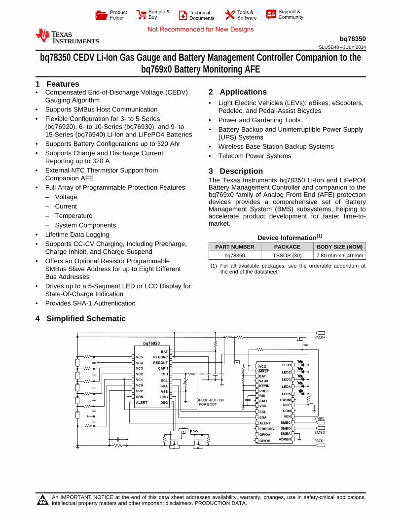
4 Simplified Schematic
1
An IMPORTANT NOTICE at the end of this data sheet addresses availability, warranty, changes, use in safety-critical applications,intellectual property matters and other important disclaimers. PRODUCTION DATA.
Not Recommended for New Designs
bq78350SLUSB48 –JULY 2014 www.ti.com
Table of Contents8.13 Typical Characteristics ......................................... 111 Features .................................................................. 1
9 Detailed Description ............................................ 122 Applications ........................................................... 19.1 Overview ................................................................. 123 Description ............................................................. 19.2 Functional Block Diagram ....................................... 124 Simplified Schematic............................................. 19.3 Feature Description................................................. 125 Revision History..................................................... 29.4 Device Functional Modes........................................ 146 Description (continued)......................................... 39.5 Programming........................................................... 157 Pin Configuration and Functions ......................... 4 10 Application and Implementation........................ 168 Specifications......................................................... 6 10.1 Application Information.......................................... 16
8.1 Absolute Maximum Ratings ...................................... 6 10.2 Typical Applications .............................................. 168.2 Handling Ratings....................................................... 6 11 Power Supply Recommendations ..................... 258.3 Recommended Operating Conditions....................... 6
12 Layout................................................................... 268.4 Thermal Information .................................................. 712.1 Layout Guidelines ................................................. 268.5 Electrical Characteristics: Supply Current................. 712.2 Layout Example .................................................... 278.6 Electrical Characteristics: I/O.................................... 7
13 Device and Documentation Support ................. 288.7 Electrical Characteristics: ADC ................................. 813.1 Related Documentation......................................... 288.8 Electrical Characteristics: Power-On Reset .............. 813.2 Trademarks ........................................................... 288.9 Electrical Characteristics: Oscillator......................... 813.3 Electrostatic Discharge Caution............................ 288.10 Electrical Characteristics: Data Flash Memory ....... 813.4 Glossary ................................................................ 288.11 Electrical Characteristics: Register Backup ............ 9
14 Mechanical, Packaging, and Orderable8.12 SMBus Timing Specifications ............................... 10Information ........................................................... 28
5 Revision History
DATE REVISION NOTESJuly 2014 * Initial Release
2 Submit Documentation Feedback Copyright © 2014, Texas Instruments Incorporated
Product Folder Links: bq78350
Not Recommended for New Designs
bq78350www.ti.com SLUSB48 –JULY 2014
6 Description (continued)The bq78350 controller and the bq769x0 AFE support from 3-series to 15-series cell applications. The bq78350provides an accurate fuel gauge and state-of-health (SoH) monitor, as well as cell balancing and a full range ofvoltage-, current-, and temperature-based protection features.
The bq78350 offers optional LED or LCD display configurations for the capacity reporting. It also makes dataavailable over its SMBus 1.1 interface. Battery history and diagnostic data is also kept within the device in non-volatile memory and is available over the same interface.
Copyright © 2014, Texas Instruments Incorporated Submit Documentation Feedback 3
Product Folder Links: bq78350
Not Recommended for New Designs
1
2
7
6
5
4
3
20
19
18
17
1615
14
SDA
SCL
PRES
PRECHG
COM
ALERT
SMBA
ADREN
VCC
VSS
MRST
VSS
VSS
SMBD
SAFE
8
13
9
10
12
11
PWRM
GPIO A
VEN
SMBC
VAUX
LED1
LED2
LED3
LED4
LED5
RBI
GPIO B
DISP
BAT
KEYIN
21
22
23
24
25
26
27
28
29
30
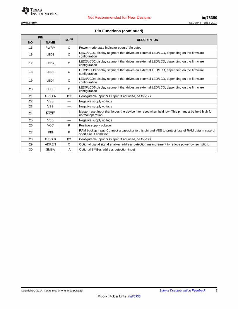
bq78350SLUSB48 –JULY 2014 www.ti.com
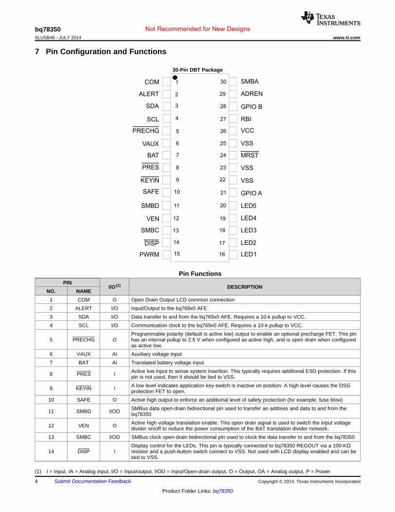
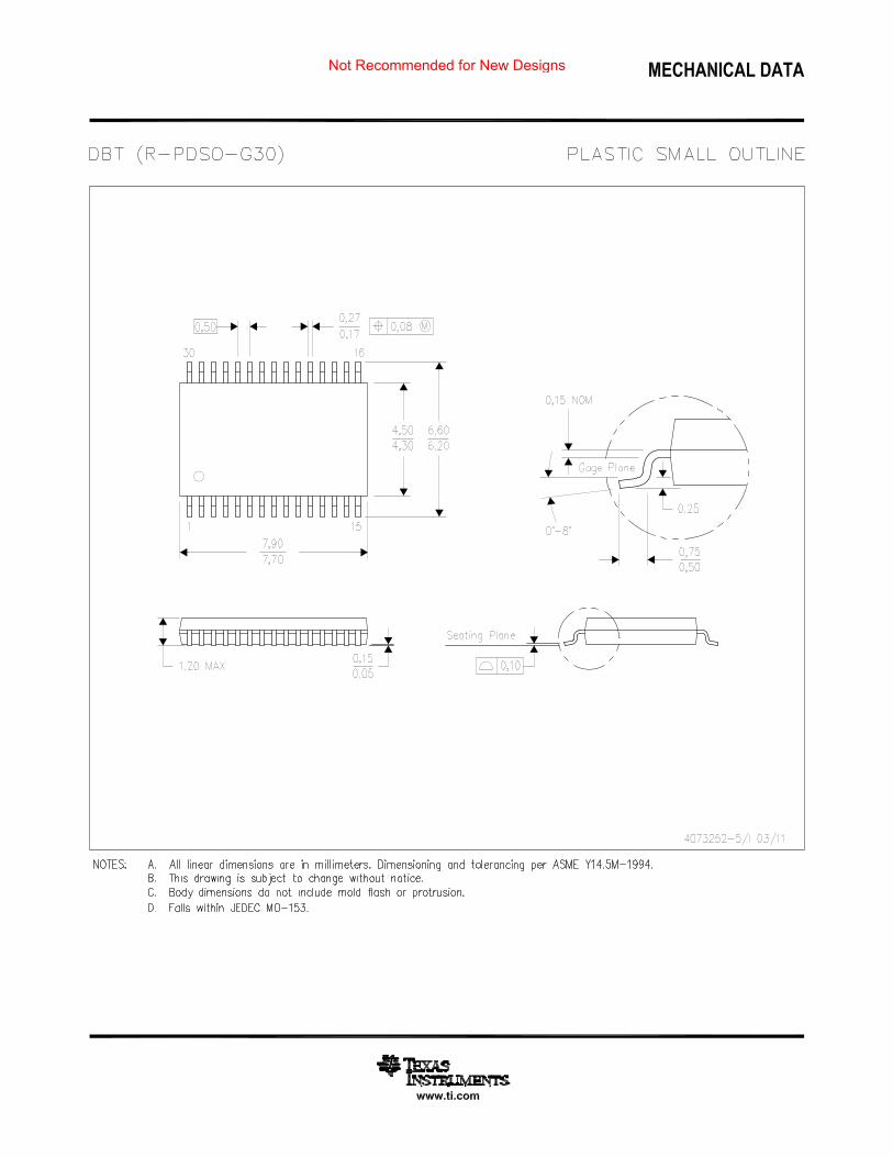
7 Pin Configuration and Functions
30-Pin DBT Package
Pin FunctionsPIN
I/O (1) DESCRIPTIONNO. NAME
1 COM O Open Drain Output LCD common connection2 ALERT I/O Input/Output to the bq769x0 AFE3 SDA I/O Data transfer to and from the bq769x0 AFE. Requires a 10-k pullup to VCC.4 SCL I/O Communication clock to the bq769x0 AFE. Requires a 10-k pullup to VCC.
Programmable polarity (default is active low) output to enable an optional precharge FET. This pin5 PRECHG O has an internal pullup to 2.5 V when configured as active high, and is open drain when configured
as active low.6 VAUX AI Auxiliary voltage input7 BAT AI Translated battery voltage input
Active low input to sense system insertion. This typically requires additional ESD protection. If this8 PRES I pin is not used, then it should be tied to VSS.A low level indicates application key-switch is inactive on position. A high level causes the DSG9 KEYIN I protection FET to open.
10 SAFE O Active high output to enforce an additional level of safety protection (for example, fuse blow)SMBus data open-drain bidirectional pin used to transfer an address and data to and from the11 SMBD I/OD bq78350Active high voltage translation enable. This open drain signal is used to switch the input voltage12 VEN O divider on/off to reduce the power consumption of the BAT translation divider network.
13 SMBC I/OD SMBus clock open-drain bidirectional pin used to clock the data transfer to and from the bq78350Display control for the LEDs. This pin is typically connected to bq78350 REGOUT via a 100-KΩ
14 DISP I resistor and a push-button switch connect to VSS. Not used with LCD display enabled and can betied to VSS.
(1) I = Input, IA = Analog input, I/O = Input/output, I/OD = Input/Open-drain output, O = Output, OA = Analog output, P = Power
4 Submit Documentation Feedback Copyright © 2014, Texas Instruments Incorporated
Product Folder Links: bq78350
Not Recommended for New Designs
bq78350www.ti.com SLUSB48 –JULY 2014
Pin Functions (continued)PIN
I/O (1) DESCRIPTIONNO. NAME15 PWRM O Power mode state indicator open drain output
LED1/LCD1 display segment that drives an external LED/LCD, depending on the firmware16 LED1 O configurationLED2/LCD2 display segment that drives an external LED/LCD, depending on the firmware17 LED2 O configurationLED3/LCD3 display segment that drives an external LED/LCD, depending on the firmware18 LED3 O configurationLED4/LCD4 display segment that drives an external LED/LCD, depending on the firmware19 LED4 O configurationLED5/LCD5 display segment that drives an external LED/LCD, depending on the firmware20 LED5 O configuration
21 GPIO A I/O Configurable Input or Output. If not used, tie to VSS.22 VSS — Negative supply voltage23 VSS — Negative supply voltage
Master reset input that forces the device into reset when held low. This pin must be held high for24 MRST I normal operation.25 VSS — Negative supply voltage26 VCC P Positive supply voltage
RAM backup input. Connect a capacitor to this pin and VSS to protect loss of RAM data in case of27 RBI P short circuit condition.28 GPIO B I/O Configurable Input or Output. If not used, tie to VSS.29 ADREN O Optional digital signal enables address detection measurement to reduce power consumption.30 SMBA IA Optional SMBus address detection input
Copyright © 2014, Texas Instruments Incorporated Submit Documentation Feedback 5
Product Folder Links: bq78350
Not Recommended for New Designs
bq78350SLUSB48 –JULY 2014 www.ti.com
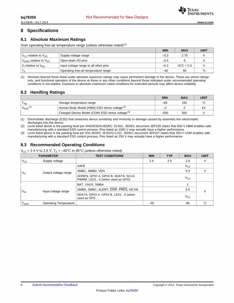
8 Specifications
8.1 Absolute Maximum RatingsOver operating free-air temperature range (unless otherwise noted) (1)
MIN MAX UNITVCC relative to VSS Supply voltage range –0.3 2.75 VV(IOD) relative to VSS Open-drain I/O pins –0.3 6 VVI relative to VSS Input voltage range to all other pins –0.3 VCC + 0.3 VTA Operating free-air temperature range –40 85 °C
(1) Stresses beyond those listed under absolute maximum ratings may cause permanent damage to the device. These are stress ratingsonly, and functional operation of the device at these or any other conditions beyond those indicated under recommended operatingconditions is not implied. Exposure to absolute–maximum–rated conditions for extended periods may affect device reliability.
8.2 Handling RatingsMIN MAX UNIT
Tstg Storage temperature range –65 150 °CVESD
(1) Human Body Model (HBM) ESD stress voltage (2) –2 2 kVCharged Device Model (CDM) ESD stress voltage (3) –500 500 V
(1) Electrostatic discharge (ESD) that measures device sensitivity and immunity to damage caused by assembly line electrostaticdischarges into the device.
(2) Level listed above is the passing level per ANSI/ESDA/JEDEC JS-001. JEDEC document JEP155 states that 500-V HBM enables safemanufacturing with a standard ESD control process. Pins listed as 1000 V may actually have a higher performance.
(3) Level listed above is the passing level per EIA-JEDEC JESD22-C101. JEDEC document JEP157 states that 250-V CDM enables safemanufacturing with a standard ESD control process. Pins listed as 250 V may actually have a higher performance.
8.3 Recommended Operating ConditionsVCC = 2.4 V to 2.6 V, TA = –40°C to 85°C (unless otherwise noted)
PARAMETER TEST CONDITIONS MIN TYP MAX UNITVCC Supply voltage 2.4 2.5 2.6 V
SAFE VCC
SMBC, SMBD, VEN 5.5 VVO Output voltage rangeADREN, GPIO A, GPIO B, SDATA, SCLK, VCCPWRM, LED1...5 (when used as GPO)BAT, VAUX, SMBA 1SMBD, SMBC, ALERT, DISP, PRES, KEYIN 5.5VIN Input voltage range VSDATA, GPIO A, GPIO B, LED1...5 (when VCCused as GPI)
TOPR Operating Temperature –40 85 °C
6 Submit Documentation Feedback Copyright © 2014, Texas Instruments Incorporated
Product Folder Links: bq78350
Not Recommended for New Designs

bq78350www.ti.com SLUSB48 –JULY 2014
8.4 Thermal Informationbq78350
THERMAL METRIC (1) TSSOP (DBT) QFN (RSM) UNIT30 PINS 32 PINS
RJA, High K Junction-to-ambient thermal resistance (2) 81.4 37.4RJC(top) Junction-to-case(top) thermal resistance (3) 16.2 30.6RJB Junction-to-board thermal resistance (4) 34.1 7.7
°C/WψJT Junction-to-top characterization parameter (5) 0.4 0.4ψJB Junction-to-board characterization parameter (6) 33.6 7.5RθJC(bottom) Junction-to-case(bottom) thermal resistance (7) n/a 2.6
(1) For more information about traditional and new thermal metrics, see the IC Package Thermal Metrics application report, SPRA953.(2) The junction-to-ambient thermal resistance under natural convection is obtained in a simulation on a JEDEC-standard, high-K board, as
specified in JESD51-7, in an environment described in JESD51-2a.(3) The junction-to-case (top) thermal resistance is obtained by simulating a cold plate test on the package top. No specific JEDEC-
standard test exists, but a close description can be found in the ANSI SEMI standard G30-88.(4) The junction-to-board thermal resistance is obtained by simulating in an environment with a ring cold plate fixture to control the PCB
temperature, as described in JESD51-8.(5) The junction-to-top characterization parameter, ψJT, estimates the junction temperature of a device in a real system and is extracted
from the simulation data for obtaining θJA, using a procedure described in JESD51-2a (sections 6 and 7).(6) The junction-to-board characterization parameter, ψJB, estimates the junction temperature of a device in a real system and is extracted
from the simulation data for obtaining θJA , using a procedure described in JESD51-2a (sections 6 and 7).(7) The junction-to-case (bottom) thermal resistance is obtained by simulating a cold plate test on the exposed (power) pad. No specific
JEDEC standard test exists, but a close description can be found in the ANSI SEMI standard G30-88.Spacer
8.5 Electrical Characteristics: Supply CurrentVCC = 2.4 V to 2.6 V, TA = –40°C to 85°C (unless otherwise noted)
PARAMETER TEST CONDITIONS MIN TYP MAX UNITICC Operating mode current No flash programming 650 (1) μAI(SLEEP) Low-power storage mode current SLEEP mode 300 (2) μAI(SHUTDOWN) Low-power SHUTDOWN mode current SHUTDOWN mode 0.1 1 μA
(1) The actual current consumption of this mode fluctuates during operation over a 1-s period. The value shown is an average using thedefault data flash configuration.
(2) The actual current consumption of this mode fluctuates during operation over a user-configurable period. The value shown is an averageusing the default data flash configuration.
8.6 Electrical Characteristics: I/OVCC = 2.4 V to 2.6 V, TA = –40°C to 85°C (unless otherwise noted)
PARAMETER TEST CONDITIONS MIN TYP MAX UNITOutput voltage low SMBC, SMBD,SDATA, SCLK, SAFE, ADREN, VEN, IOL = 0.5 mA 0.4 VGPIO A, GPIO B, PWRMVOLOutput voltage low LED1, LED2, LED3, IOL = 3 mA 0.4LED4, LED5Output voltage high SMBC, SMBD,
VOH SDATA, SCLK, SAFE, ADREN, VEN, IOH = –1 mA VCC – 0.5 VGPIO A, GPIO B, PWRMInput voltage low SMBC, SMBD, SDATA,
VIL SCLK, ALERT, DISP, SMBA, GPIO A, –0.3 0.8 VGPIO B, PRES, KEYINInput voltage high SMBC, SMBD,SDATA, SCLK, ALERT, SMBA, GPIO A, 2 6 V
VIH GPIO BInput voltage high DISP, PRES, KEYIN 2 VCC + 0.3 V
CIN Input capacitance 5 pFILKG Input leakage current 1 µA
Copyright © 2014, Texas Instruments Incorporated Submit Documentation Feedback 7
Product Folder Links: bq78350
Not Recommended for New Designs
bq78350SLUSB48 –JULY 2014 www.ti.com
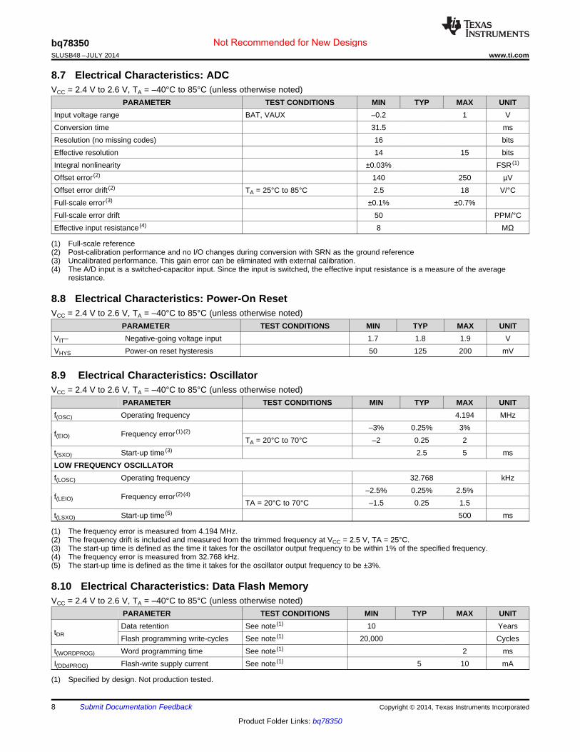
8.7 Electrical Characteristics: ADCVCC = 2.4 V to 2.6 V, TA = –40°C to 85°C (unless otherwise noted)
PARAMETER TEST CONDITIONS MIN TYP MAX UNITInput voltage range BAT, VAUX –0.2 1 VConversion time 31.5 msResolution (no missing codes) 16 bitsEffective resolution 14 15 bitsIntegral nonlinearity ±0.03% FSR (1)
Offset error (2) 140 250 µVOffset error drift (2) TA = 25°C to 85°C 2.5 18 V/°CFull-scale error (3) ±0.1% ±0.7%Full-scale error drift 50 PPM/°CEffective input resistance (4) 8 MΩ
(1) Full-scale reference(2) Post-calibration performance and no I/O changes during conversion with SRN as the ground reference(3) Uncalibrated performance. This gain error can be eliminated with external calibration.(4) The A/D input is a switched-capacitor input. Since the input is switched, the effective input resistance is a measure of the average
resistance.
8.8 Electrical Characteristics: Power-On ResetVCC = 2.4 V to 2.6 V, TA = –40°C to 85°C (unless otherwise noted)
PARAMETER TEST CONDITIONS MIN TYP MAX UNITVIT– Negative-going voltage input 1.7 1.8 1.9 VVHYS Power-on reset hysteresis 50 125 200 mV
8.9 Electrical Characteristics: OscillatorVCC = 2.4 V to 2.6 V, TA = –40°C to 85°C (unless otherwise noted)
PARAMETER TEST CONDITIONS MIN TYP MAX UNITf(OSC) Operating frequency 4.194 MHz
–3% 0.25% 3%f(EIO) Frequency error (1) (2)
TA = 20°C to 70°C –2 0.25 2t(SXO) Start-up time (3) 2.5 5 msLOW FREQUENCY OSCILLATORf(LOSC) Operating frequency 32.768 kHz
–2.5% 0.25% 2.5%f(LEIO) Frequency error (2) (4)
TA = 20°C to 70°C –1.5 0.25 1.5t(LSXO) Start-up time (5) 500 ms
(1) The frequency error is measured from 4.194 MHz.(2) The frequency drift is included and measured from the trimmed frequency at VCC = 2.5 V, TA = 25°C.(3) The start-up time is defined as the time it takes for the oscillator output frequency to be within 1% of the specified frequency.(4) The frequency error is measured from 32.768 kHz.(5) The start-up time is defined as the time it takes for the oscillator output frequency to be ±3%.
8.10 Electrical Characteristics: Data Flash MemoryVCC = 2.4 V to 2.6 V, TA = –40°C to 85°C (unless otherwise noted)
PARAMETER TEST CONDITIONS MIN TYP MAX UNITData retention See note (1) 10 Years
tDR Flash programming write-cycles See note (1) 20,000 Cyclest(WORDPROG) Word programming time See note (1) 2 msI(DDdPROG) Flash-write supply current See note (1) 5 10 mA
(1) Specified by design. Not production tested.
8 Submit Documentation Feedback Copyright © 2014, Texas Instruments Incorporated
Product Folder Links: bq78350
Not Recommended for New Designs
bq78350www.ti.com SLUSB48 –JULY 2014
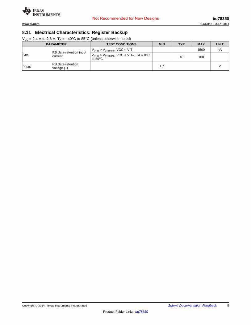
8.11 Electrical Characteristics: Register BackupVCC = 2.4 V to 2.6 V, TA = –40°C to 85°C (unless otherwise noted)
PARAMETER TEST CONDITIONS MIN TYP MAX UNITV(RB) > V(RBMIN), VCC < VIT– 1500 nA
RB data-retention inputI(RB) V(RB) > V(RBMIN), VCC < VIT–, TA = 0°Ccurrent 40 160to 50°CRB data-retentionV(RB) 1.7 Vvoltage (1)
Copyright © 2014, Texas Instruments Incorporated Submit Documentation Feedback 9
Product Folder Links: bq78350
Not Recommended for New Designs
bq78350SLUSB48 –JULY 2014 www.ti.com
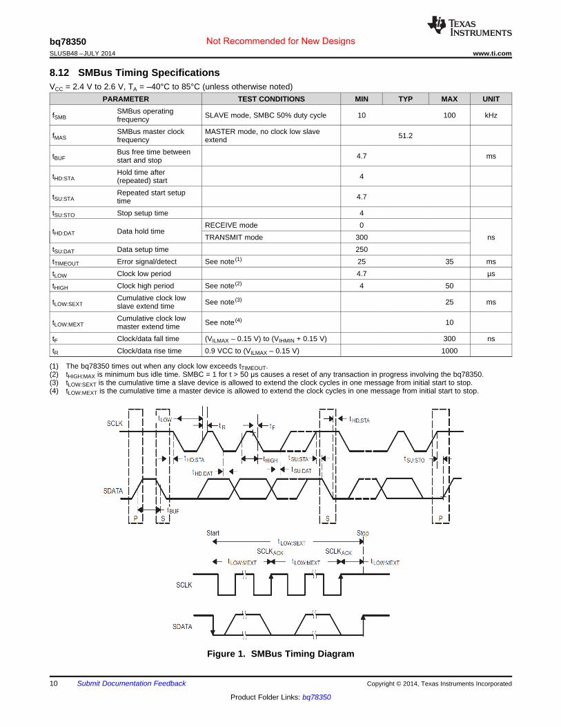
8.12 SMBus Timing SpecificationsVCC = 2.4 V to 2.6 V, TA = –40°C to 85°C (unless otherwise noted)
PARAMETER TEST CONDITIONS MIN TYP MAX UNITSMBus operatingfSMB SLAVE mode, SMBC 50% duty cycle 10 100 kHzfrequencySMBus master clock MASTER mode, no clock low slavefMAS 51.2frequency extendBus free time betweentBUF 4.7 msstart and stopHold time aftertHD:STA 4(repeated) startRepeated start setuptSU:STA 4.7time
tSU:STO Stop setup time 4RECEIVE mode 0
tHD:DAT Data hold timeTRANSMIT mode 300 ns
tSU:DAT Data setup time 250tTIMEOUT Error signal/detect See note (1) 25 35 mstLOW Clock low period 4.7 µstHIGH Clock high period See note (2) 4 50
Cumulative clock lowtLOW:SEXT See note (3) 25 msslave extend timeCumulative clock lowtLOW:MEXT See note (4) 10master extend time
tF Clock/data fall time (VILMAX – 0.15 V) to (VIHMIN + 0.15 V) 300 nstR Clock/data rise time 0.9 VCC to (VILMAX – 0.15 V) 1000
(1) The bq78350 times out when any clock low exceeds tTIMEOUT.(2) tHIGH:MAX is minimum bus idle time. SMBC = 1 for t > 50 μs causes a reset of any transaction in progress involving the bq78350.(3) tLOW:SEXT is the cumulative time a slave device is allowed to extend the clock cycles in one message from initial start to stop.(4) tLOW:MEXT is the cumulative time a master device is allowed to extend the clock cycles in one message from initial start to stop.
Figure 1. SMBus Timing Diagram
10 Submit Documentation Feedback Copyright © 2014, Texas Instruments Incorporated
Product Folder Links: bq78350
Not Recommended for New Designs
4.160
4.165
4.170
4.175
4.180
4.185
4.190
±40 ±20 0 20 40 60 80
HF
O
Fre
quen
cy (
MH
z)
Temperature (C) C005
2.55
2.60
2.65
2.70
2.75
2.80
2.85
2.90
2.95
3.00
3.05
±40 ±20 0 20 40 60 80
LED
Sin
k C
urre
nt (
mA
)
Temperature (C) C003
32.55
32.60
32.65
32.70
32.75
32.80
32.85
±40 ±20 0 20 40 60 80
LFO
F
requ
ency
(kH
z)
Temperature (C) C004
171.0
171.5
172.0
172.5
173.0
173.5
174.0
174.5
±40 ±20 0 20 40 60 80
AD
C O
ffset
Err
or (
V)
Temperature (C) C002
1.2230
1.2235
1.2240
1.2245
1.2250
1.2255
1.2260
1.2265
1.2270
1.2275
1.2280
±40 ±20 0 20 40 60 80
Inte
rnal
Vol
tage
Ref
eren
ce (
V)
Temperature (C) C001
bq78350www.ti.com SLUSB48 –JULY 2014
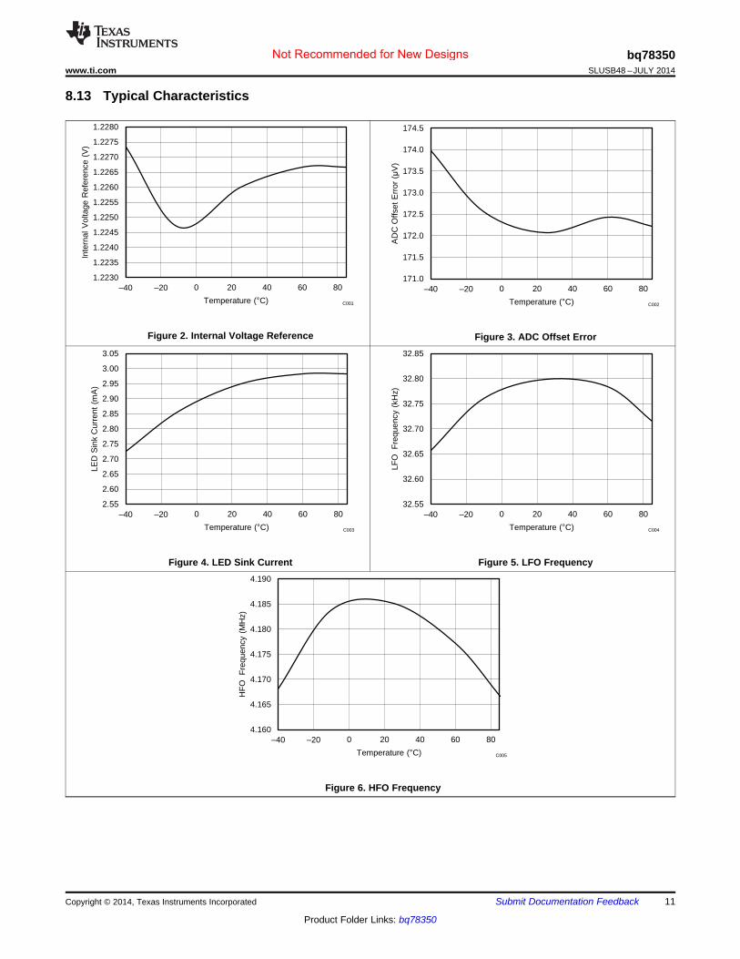
8.13 Typical Characteristics
Figure 2. Internal Voltage Reference Figure 3. ADC Offset Error
Figure 4. LED Sink Current Figure 5. LFO Frequency
Figure 6. HFO Frequency
Copyright © 2014, Texas Instruments Incorporated Submit Documentation Feedback 11
Product Folder Links: bq78350
Not Recommended for New Designs
Input/OutputOscillator
System Clock
Power
Regulation
ANDManagement
CoolRISC
CPU
Program Memory Data MemoryCommunications
SMBus
Peripheralsand
Timers
Interrupt
Controller
Analog Front EndDelta-Sigma ADC
AND
Integrating
Coulomb CounterDMAddr (16-bit)
Data (8-bit)
PMAddr
(15-bit)PMInst
(22-bit)
32 kHz
System ClocksReset*
2
1
8 88
Interrupt *
Event*
SRP
SRN
VCC
VSS
MRST
RBI
COM, ALERT,KEYIN, SAFE,
SMBD, SMBC,
VEN,DISP
GPIOA
GPIOB
LED1...5
PWRM
SMBA, ADREN,SDA, SCL,
PRECHG,VAUX,BAT, PRES
System I /O (13-bit)
Wake ComparatorEvent*
bq78350SLUSB48 –JULY 2014 www.ti.com
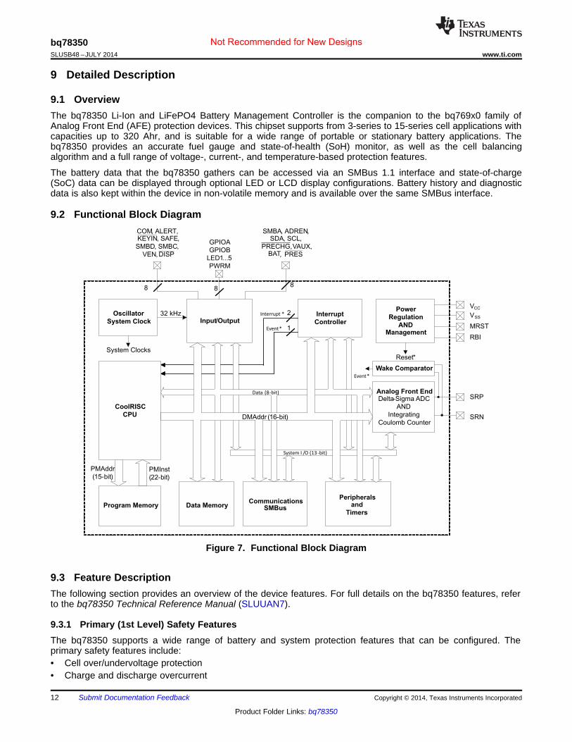
9 Detailed Description
9.1 OverviewThe bq78350 Li-Ion and LiFePO4 Battery Management Controller is the companion to the bq769x0 family ofAnalog Front End (AFE) protection devices. This chipset supports from 3-series to 15-series cell applications withcapacities up to 320 Ahr, and is suitable for a wide range of portable or stationary battery applications. Thebq78350 provides an accurate fuel gauge and state-of-health (SoH) monitor, as well as the cell balancingalgorithm and a full range of voltage-, current-, and temperature-based protection features.
The battery data that the bq78350 gathers can be accessed via an SMBus 1.1 interface and state-of-charge(SoC) data can be displayed through optional LED or LCD display configurations. Battery history and diagnosticdata is also kept within the device in non-volatile memory and is available over the same SMBus interface.
9.2 Functional Block Diagram
Figure 7. Functional Block Diagram
9.3 Feature DescriptionThe following section provides an overview of the device features. For full details on the bq78350 features, referto the bq78350 Technical Reference Manual (SLUUAN7).
9.3.1 Primary (1st Level) Safety FeaturesThe bq78350 supports a wide range of battery and system protection features that can be configured. Theprimary safety features include:• Cell over/undervoltage protection• Charge and discharge overcurrent
12 Submit Documentation Feedback Copyright © 2014, Texas Instruments Incorporated
Product Folder Links: bq78350
Not Recommended for New Designs
bq78350www.ti.com SLUSB48 –JULY 2014
Feature Description (continued)• Short circuit protection• Charge and discharge overtemperature with independent alarms and thresholds for each thermistor
9.3.2 Secondary (2nd Level) Safety FeaturesThe secondary safety features of the bq78350 can be used to indicate more serious faults via the SAFE pin. Thispin can be used to blow an in-line fuse to permanently disable the battery pack from charging or discharging. Thesecondary safety protection features include:• Safety overvoltage• Safety undervoltage• Safety overcurrent in charge and discharge• Safety overtemperature in charge and discharge• Charge FET and Precharge FET fault• Discharge FET fault• Cell imbalance detection• Open thermistor detection• AFE communication fault
9.3.3 Charge Control FeaturesThe bq78350 charge control features include:• Provides a range of options to configure the charging algorithm and its actions based on the application
requirements• Reports the appropriate charging current needed for constant current charging, and the appropriate charging
voltage needed for constant voltage charging• Supports pre-charging/0-volt charging• Supports charge inhibit and charge suspend if battery pack temperature is out of temperature range
9.3.4 Fuel GaugingThe bq78350 uses Compensated End-of-Discharge Voltage (CEDV) technology to measure and calculate theavailable charge in battery cells. The bq78350 accumulates a measure of charge and discharge currents andcompensates the charge current measurement for the temperature and state-of-charge of the battery. Thebq78350 estimates self-discharge of the battery and also adjusts the self-discharge estimation based ontemperature.
9.3.5 Lifetime Data LoggingThe bq78350 offers lifetime data logging, where important measurements are stored for warranty and analysispurposes. The data monitored includes:• Lifetime maximum temperature• Lifetime minimum temperature• Lifetime maximum battery cell voltage per cell• Lifetime minimum battery cell voltage per cell• Cycle count• Maximum charge current• Maximum discharge current• Safety events that trigger SafetyStatus() updates. (The 12 most common are tracked.)
9.3.6 AuthenticationThe bq78350 supports authentication by the host using SHA-1.
Copyright © 2014, Texas Instruments Incorporated Submit Documentation Feedback 13
Product Folder Links: bq78350
Not Recommended for New Designs
bq78350SLUSB48 –JULY 2014 www.ti.com
Feature Description (continued)9.3.7 Battery Parameter MeasurementsThe bq78350 digitally reads bq769x0 registers containing recent values from the integrating analog-to-digitalconverter (CC) for current measurement and a second delta-sigma ADC for individual cell and temperaturemeasurements.
9.3.7.1 Current and Coulomb CountingThe integrating delta-sigma ADC (CC) in the companion bq769x0 AFE measures the charge/discharge flow ofthe battery by measuring the voltage drop across a small-value sense resistor between the SRP and SRN pins.The 15-bit integrating ADC measures bipolar signals from –0.20 V to 0.20 V with 15-µV resolution. The AFEreports charge activity when VSR = V(SRP) – V(SRN) is positive, and discharge activity when VSR = V(SRP) – V(SRN)is negative. The bq78350 continuously monitors the measured current and integrates the digital signal from theAFE over time, using an internal counter.
To support large battery configurations, the current data can be scaled to ensure accurate reporting through theSMBus. The data reported is scaled based on the setting of the SpecificationInfo() command.
9.3.7.2 VoltageThe bq78350 updates the individual series cell voltages through the bq769x0 at 1-s intervals. The bq78350configures the bq769x0 to connect to the selected cells in sequence and uses this information for cell balancingand individual cell fault functions. The internal 14-bit ADC of the bq769x0 measures each cell voltage value,which is then communicated digitally to the bq78350 where they are scaled and translated into unit mV. Themaximum supported input range of the ADC is 6.075 V.
The bq78350 also separately measures the average cell voltage through an external translation circuit at theBAT pin. This value is specifically used for the fuel gauge algorithm. The external translation circuit is controlledvia the VEN pin so that the translation circuit is only enabled when required to reduce overall powerconsumption. For correct operation, VEN requires an external pull-up to VCC, typically 100 k.
In addition to the voltage measurements used by the bq78350 algorithms, there is an optional auxiliary voltagemeasurement capability via the VAUX pin. This feature measures the input on a 1-s update rate and provides theprogrammable scaled value through an SMBus command.
To support large battery configurations, the voltage data can be scaled to ensure accurate reporting through theSMBus. The data reported is scaled based on the setting of the SpecificationInfo() command.
9.3.7.3 TemperatureThe bq78350 receives temperature information from external or internal temperature sensors in the bq769x0AFE. Depending on the number of series cells supported, the AFE will provide one, two, or three externalthermistor measurements.
9.4 Device Functional ModesThe bq78350 supports three power modes to optimize the power consumption:• In NORMAL mode, the bq78350 performs measurements, calculations, protection decisions, and data
updates in 1-s intervals. Between these intervals, the bq78350 is in a reduced power mode.• In SLEEP mode, the bq78350 performs measurements, calculations, protection decisions, and data updates
in adjustable time intervals. Between these intervals, the bq78350 is in a reduced power mode.• In SHUTDOWN mode, the bq78350 is completely powered down.
The bq78350 indicates through the PWRM pin which power mode it is in. This enables other circuits to changebased on the power mode detection criteria of the bq78350.
14 Submit Documentation Feedback Copyright © 2014, Texas Instruments Incorporated
Product Folder Links: bq78350
Not Recommended for New Designs
bq78350www.ti.com SLUSB48 –JULY 2014
9.5 Programming
9.5.1 Physical InterfaceThe bq78350 uses SMBus 1.1 with packet error checking (PEC) as an option and is used as a slave only.
9.5.2 SMBus AddressThe bq78350 determines its SMBus 1.1 slave address through a voltage on SMBA, Pin 30. The voltage is setwith a pair of high value resistors if an alternate address is required and is measured either upon exit of POR orwhen system present is detected. ADREN, Pin 29, may be used to disable the voltage divider after use to reducepower consumption.
9.5.3 SMBus On and Off StateThe bq78350 detects an SMBus off state when SMBC and SMBD are logic-low for ≥ 2 seconds. Clearing thisstate requires either SMBC or SMBD to transition high. Within 1 ms, the communication bus is available.
Copyright © 2014, Texas Instruments Incorporated Submit Documentation Feedback 15
Product Folder Links: bq78350
Not Recommended for New Designs
bq78350SLUSB48 –JULY 2014 www.ti.com
10 Application and Implementation
10.1 Application InformationThe bq78350 Battery Management Controller companion to the bq769x0 family of battery monitoring AFEsenables many standard and enhanced battery management features in a 3-series to 15-series Li-Ion/Li Polymerbattery pack.
To design and implement a complete solution, users need the Battery Management Studio (bqSTUDIO) tool toconfigure a "golden image" set of parameters for a specific battery pack and application. The bqSTUDIO tool is agraphical user-interface tool installed on a PC during development. The firmware installed in the product hasdefault values, which are summarized in the bq78350 Technical Reference Manual (SLUUAN7). With thebqSTUDIO tool, users can change these default values to cater to specific application requirements. Once thesystem parameters are known (for example, fault trigger thresholds for protection, enable/disable of certainfeatures for operation, configuration of cells, among others), the data can be saved. This data is referred to asthe "golden image.”
10.2 Typical ApplicationsThe bq78350 can be used with the bq76920, bq76930, or bq76940 device, but as default it is setup for a 5-seriescell, 4400-mA battery application using the bq76920 AFE.
16 Submit Documentation Feedback Copyright © 2014, Texas Instruments Incorporated
Product Folder Links: bq78350
Not Recommended for New Designs
NC
1
AL
ER
T2
SD
A3
SC
L4
PR
EC
HG
5
VA
UX
6
BA
T7
PR
ES
8
KE
YIN
9
SA
FE
10
SM
BD
11
VE
N1
2
SM
BC
13
DIS
P1
4
PW
RM
15
LE
D1
16
LE
D2
17
LE
D3
18
LE
D4
19
LE
D5
20
VS
S2
1
VS
S2
2
VS
S2
3
MR
ST
24
VS
S2
5
VC
C2
6
RB
I2
7
NC
28
AD
RE
N2
9
SM
BA
30
U2
BQ
78
35
0D
BT
GN
DG
ND
0.1
µF
C2
4
100k
R55
221k
R57
GN
D
0.1
µF
C2
5
GN
D
300k
25
pp
m/C
R4
7
13
.7k
R4
8
Q9
CS
D1
73
81
F4
Q8
BS
S8
4-7
-F
100k
R5
0
100k
R49
GN
DG
ND
3300pF
C2
3
1.0
0M
eg
R5
1
BA
TT
+
PR
E
AL
ER
T
SD
A
SC
L
RE
GO
UT
100
R7
7
100
R72
100
R80
100
R70
41 2 3
J4
GN
D
E2
E4
1.0
0M
eg
R7
61
.00
Me
gR
73
GN
D
5.6
V
D3
2
5.6
V
D3
0
SM
B
SM
B is r
eq
uir
ed
for
gauge
se
tup
.S
ign
als
wo
uld
re
qu
ire
iso
latio
ncir
cu
it for
use
insyste
m
BA
TT-
bq78350www.ti.com SLUSB48 –JULY 2014
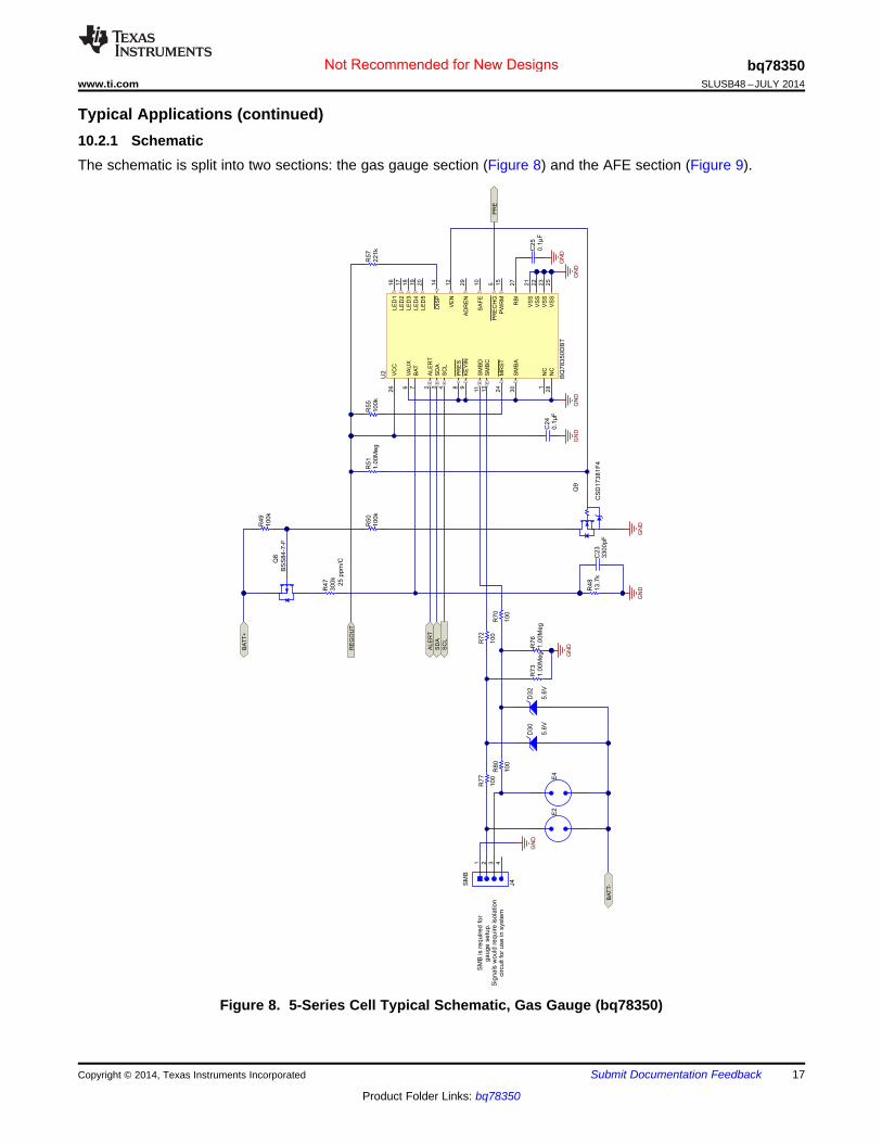
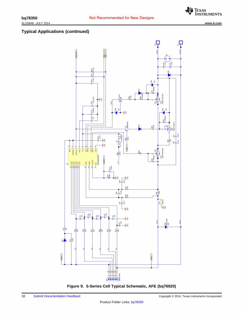
Typical Applications (continued)10.2.1 SchematicThe schematic is split into two sections: the gas gauge section (Figure 8) and the AFE section (Figure 9).
Figure 8. 5-Series Cell Typical Schematic, Gas Gauge (bq78350)
Copyright © 2014, Texas Instruments Incorporated Submit Documentation Feedback 17
Product Folder Links: bq78350
Not Recommended for New Designs
DS
G1
CH
G2
VS
S3
SD
A4
SC
L5
TS
16
CA
P1
7
RE
GO
UT
8
RE
GS
RC
9
BA
T1
0
NC
11
VC
51
2
VC
41
3
VC
31
4
VC
21
5
VC
11
6
VC
01
7
SR
P1
8
SR
N1
9
AL
ER
T2
0
U1
BQ
76
92
00
0P
W
4.7
µF
C2
1
49
9k
R3
5
10
.0k
R4
21
0.0
kR
41
GN
D
GN
D
1µ
FC
16
10
.0k o
hm
t°RT
14
70
0p
FC
18
GN
D
1 2
3 4
S1
4-1
43
75
65
-13
.01
k
R3
6
47
0p
FC
13
C1
2.2
µF
C1
5
GN
DA
LE
RT
SD
A
SC
L
RE
GO
UT
4
7,8
1,2
,3
5,6
,
Q1
2C
SD
17
50
1Q
5A
D2
9
1.0
0M
eg
R7
11
.00
Me
gR
62
GN
D
GN
D
0.1
µF
C3
0
0.1
µF
C3
1
0.1
µF
C3
3
0.1
µF
C3
2
0R6
3
1.0
0k
R6
9
1.0
0M
eg
R6
8
16
V
D2
8
D2
7
E1
PA
CK
+
4
7,8
1,2
,3
5,6
,
Q1
5C
SD
17
50
1Q
5A
1J3
1J2
Q1
6
CH
G
1.0
0M
eg
R6
7
1.0
k
R6
4
Q1
4M
MB
TA
92
10
.0k
R6
6D2
4
10
.0k
R6
5
10
V
D2
5
3
1
2
Q1
3C
SD
17
38
1F
4
18
V
D2
6
PA
CK
-
PR
E
1µ
FC
4
1µ
FC
1
10
0
R1
5
10
0
R1
3
GN
D
C4
C3
C1
C0
541 2 3 6
J1
39
50
21
00
6
C2
C5
1µ
FC
3
GN
D
10
0
R1
61
µF
C5
10
0
R1
71
µF
C6
10
0
R1
81
µF
C7
10
0
R1
9C
5
C4
C3
C2
C1
C0
D11
10
.0k
R11
10
0
R1
2
BA
TT
-
0.0
01
R6
0
10
0R
59
10
0R
61
0.1
µF
C2
8
0.1
µF
C2
9
0.1
µF
C2
7
GN
D
28
V
D2
3S
MC
J2
8A
BA
TT-
BA
TT
+
NT
1
Ne
t-T
ie
GN
D
BA
TT
+
bq78350SLUSB48 –JULY 2014 www.ti.com
Typical Applications (continued)
Figure 9. 5-Series Cell Typical Schematic, AFE (bq76920)
18 Submit Documentation Feedback Copyright © 2014, Texas Instruments Incorporated
Product Folder Links: bq78350
Not Recommended for New Designs
bq78350www.ti.com SLUSB48 –JULY 2014
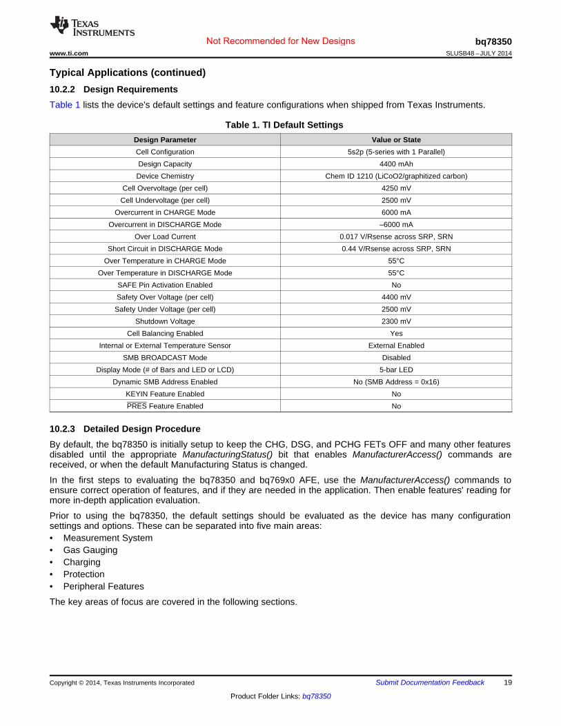
Typical Applications (continued)10.2.2 Design RequirementsTable 1 lists the device's default settings and feature configurations when shipped from Texas Instruments.
Table 1. TI Default SettingsDesign Parameter Value or StateCell Configuration 5s2p (5-series with 1 Parallel)Design Capacity 4400 mAhDevice Chemistry Chem ID 1210 (LiCoO2/graphitized carbon)
Cell Overvoltage (per cell) 4250 mVCell Undervoltage (per cell) 2500 mV
Overcurrent in CHARGE Mode 6000 mAOvercurrent in DISCHARGE Mode –6000 mA
Over Load Current 0.017 V/Rsense across SRP, SRNShort Circuit in DISCHARGE Mode 0.44 V/Rsense across SRP, SRN
Over Temperature in CHARGE Mode 55°COver Temperature in DISCHARGE Mode 55°C
SAFE Pin Activation Enabled NoSafety Over Voltage (per cell) 4400 mVSafety Under Voltage (per cell) 2500 mV
Shutdown Voltage 2300 mVCell Balancing Enabled Yes
Internal or External Temperature Sensor External EnabledSMB BROADCAST Mode Disabled
Display Mode (# of Bars and LED or LCD) 5-bar LEDDynamic SMB Address Enabled No (SMB Address = 0x16)
KEYIN Feature Enabled NoPRES Feature Enabled No
10.2.3 Detailed Design ProcedureBy default, the bq78350 is initially setup to keep the CHG, DSG, and PCHG FETs OFF and many other featuresdisabled until the appropriate ManufacturingStatus() bit that enables ManufacturerAccess() commands arereceived, or when the default Manufacturing Status is changed.
In the first steps to evaluating the bq78350 and bq769x0 AFE, use the ManufacturerAccess() commands toensure correct operation of features, and if they are needed in the application. Then enable features' reading formore in-depth application evaluation.
Prior to using the bq78350, the default settings should be evaluated as the device has many configurationsettings and options. These can be separated into five main areas:• Measurement System• Gas Gauging• Charging• Protection• Peripheral Features
The key areas of focus are covered in the following sections.
Copyright © 2014, Texas Instruments Incorporated Submit Documentation Feedback 19
Product Folder Links: bq78350
Not Recommended for New Designs
bq78350SLUSB48 –JULY 2014 www.ti.com
10.2.3.1 Measurement System
10.2.3.1.1 Cell Voltages
The bq78350 is required to be configured in the AFE Cell Map register to determine which cells to measurebased on the physical connections to the bq76920 AFE. The cell voltage data is available throughCellVoltage1()…CellVoltage5(). The cell voltages are reported as they are physically stacked. For example, if thedevice is configured for 3-series cells connected to VC1, VC2, and VC5 per the AFE Cell Map, then the cellvoltages are still reported via CellVoltage1(), CellVoltage2(), and CellVoltage3(), respectively.
For improved accuracy, offset calibration is available for each of these values and can be managed through thebqSTUDIO tool. The procedure for calibration is described in the bq78350 Technical Reference Manual(SLUUAN7) in the "Calibration" chapter.
10.2.3.1.2 External Average Cell Voltage
This is enabled by default (DA Configuration [ExtAveEN] = 1) and uses the external resistor divider connectedto the VEN and BAT pins to determine the average cell voltage of the battery pack. The average cell voltage isavailable through ExtAveCellVoltage().
CAUTIONCare should be taken in the selection of the resistor and FETs used in this dividercircuit as the tolerance and temperature drift of these components can causeincreased measurement error and a gas gauging error if CEDV Gauging Config[ExtAveCell] = 1 (default = 1).
For improved accuracy, offset and Gain calibration is available for this value and can be managed through thebqSTUDIO tool. The procedure for calibration is described in the bq78350 Technical Reference Manual(SLUUAN7) in the "Calibration" chapter.
10.2.3.1.3 Current
Current data is taken from the bq76920 and made available through Current(). The selection of the current senseresistor connected to SRP and SRN of the bq76920 is very important and there are several factors involved.
The aim of the sense resistor selection is to use the widest ADC input voltage range possible.
To maximize accuracy, the sense resistor value should be calculated based on the following formula:RSNS(min) = V(SRP) – V(SRN) / I(max) (1)Where: |V(SRP) – V(SRN)| = 200 mVI(max) = Maximum magnitude of charge of discharge current (transient or DC)
NOTERSNS(min) should include tolerance, temperature drift over the application temperature,and PCB layout tolerances when selecting the actual nominal resistor value.
When selecting the RSNS value, be aware that when selecting a small value, for example,1 mΩ, then the resolution of the current measurement will be > 1 mA. In the example ofRSNS = 1 mΩ, the current LSB will be 8.44 mA.
For improved accuracy, offset and gain calibration are available for this value and can be managed through thebqSTUDIO tool. The procedure for calibration is described in the bq78350 Technical Reference Manual(SLUUAN7) in the "Calibration" chapter.
10.2.3.1.4 Temperature
By default, the 78350 uses an external negative temperature coefficient (NTC) thermistor connected to thebq76920 as the source for the Temperature() data. The measurement uses a polynomial expression to transformthe bq76920 ADC measurement into 0.1°C resolution temperature measurement. The default polynomialcoefficients are calculated using the Semitec 103AT, although other resistances and manufacturers can be used.
20 Submit Documentation Feedback Copyright © 2014, Texas Instruments Incorporated
Product Folder Links: bq78350
Not Recommended for New Designs

bq78350www.ti.com SLUSB48 –JULY 2014
To calculate the External Temp Model coefficients, use the bq78350 Family Thermistor Coefficient Calculatorshown in the application note, Using the bq78350 (SLUA726).
For improved accuracy, offset calibration is available for this value and can be managed through the bqSTUDIOtool. The procedure for calibration is described in the bq78350 Technical Reference Manual (SLUUAN7) in the"Calibration" chapter.
10.2.3.2 Gas GaugingThe default battery chemistry (Chem ID) is 1210, which is a Li-CoO2 type chemistry. Other secondary Li-Ionbased Chem IDs can be obtained from MathCAD Chemistry Selection Tool (SLUC138).
The default maximum capacity of the battery is 4400 mAh and this should be changed based on the cell andbattery configuration chosen.
QMAX = Design Capacity of the Cell × # of parallel cellsWhere: Design Capacity of the Cell can be taken from the manufacturer data sheet.
The CEDV gas gauging algorithm requires seven coefficients to enable accurate gas gauging. The default valuesare generic for Li-CoO2 chemistry, but for accurate gas gauging these coefficients should be re-calculated. Theprocedure to gather the required data and generate the coefficients can be found athttp://www.ti.com/tool/GAUGEPARCAL.
10.2.3.3 ChargingThe charging algorithm in the bq78350 is configured to support Constant Voltage/Constant Current (CC/CV)charging of a nominal 18-V, 4400-mAh battery.
10.2.3.3.1 Fast Charging Voltage
The charging voltage is configured (Fast Charging: Voltage) based on an individual cell basis (for example, 4200mV), but the ChargingVoltage() is reported as the required battery voltage (for example, 4200 mV × 5 =21000 mV).
10.2.3.3.2 Fast Charging Current
The fast charging current is configured to 2000 mA (Fast Charging: Current) by default, which is conservative forthe majority of 4400-mAh battery applications. This should be configured based on the battery configuration, cellmanufacturer's data sheet, and system power design requirements.
10.2.3.3.3 Other Charging Modes
The bq78350 is configured to limit, through external components, and report either low or 0 ChargingVoltage()and ChargingCurrent(), based on temperature, voltage, and fault status information.
The "Charge Algorithm" section of the bq78350 Technical Reference Manual (SLUUAN7) details these featuresand settings.
10.2.3.4 ProtectionThe safety features and settings of the bq78350 are configured conservatively and are suitable for benchevaluation. However, in many cases, users will need to change these values to meet system requirements.These values should not be changed to exceed the safe operating limits provided by the cell manufacturer andany industry standard.
For details on the safety features and settings, see the "Protections" and "Permanent Fail" sections of thebq78350 Technical Reference Manual (SLUUAN7).
10.2.3.5 Peripheral Features
10.2.3.5.1 LED Display
The bq78350 is configured by default to display up to five LEDs in a bar graph configuration based on the valueof RemainingStateOfCharge() (RSOC). Each LED represents 20% of RSOC and is illuminated when thebq78350 DISP pin transitions low, and remains on for a programmable period of time.
Copyright © 2014, Texas Instruments Incorporated Submit Documentation Feedback 21
Product Folder Links: bq78350
Not Recommended for New Designs
bq78350SLUSB48 –JULY 2014 www.ti.com
In addition to many other options, the number of LEDs used and the percentage at which they can be illuminatedare configurable.
10.2.3.5.2 SMBus Address
Although the SMBus slave address is a configurable value in the bq78350, this feature is disabled by default andthe slave address is 0x16. The SMBus Address feature can allow up to nine different addresses based onexternal resistor value variation per address.
The default setup of the bq78350 is generic, but there are many additional features that can be enabled andconfigured to support a variety of system requirements. These are detailed in the bq78350 Technical ReferenceManual (SLUUAN7).
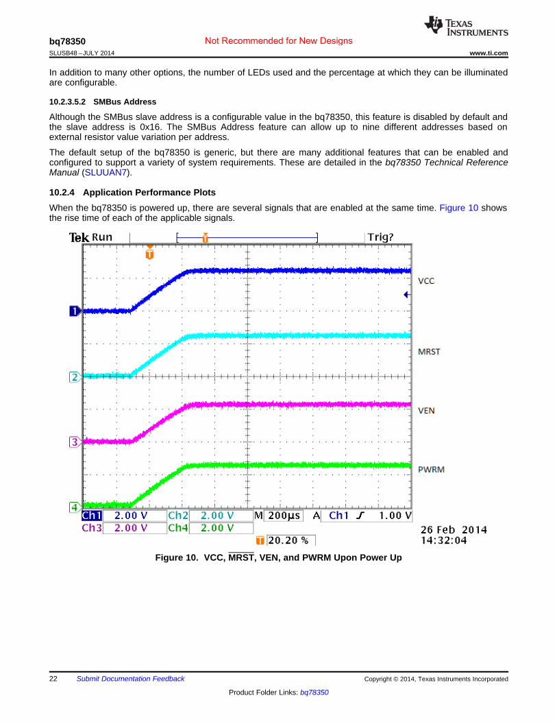
10.2.4 Application Performance PlotsWhen the bq78350 is powered up, there are several signals that are enabled at the same time. Figure 10 showsthe rise time of each of the applicable signals.
Figure 10. VCC, MRST, VEN, and PWRM Upon Power Up
22 Submit Documentation Feedback Copyright © 2014, Texas Instruments Incorporated
Product Folder Links: bq78350
Not Recommended for New Designs
bq78350www.ti.com SLUSB48 –JULY 2014
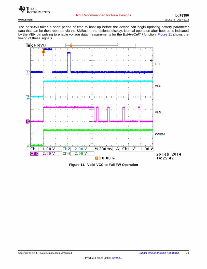
The bq78350 takes a short period of time to boot up before the device can begin updating battery parameterdata that can be then reported via the SMBus or the optional display. Normal operation after boot-up is indicatedby the VEN pin pulsing to enable voltage data measurements for the ExtAveCell( ) function. Figure 11 shows thetiming of these signals.
Figure 11. Valid VCC to Full FW Operation
Copyright © 2014, Texas Instruments Incorporated Submit Documentation Feedback 23
Product Folder Links: bq78350
Not Recommended for New Designs
±10
±8
±6
±4
±2
0
2
4
6
8
10
±20 0 20 40 60 80
Cur
rent
Err
or (
mA
)
Forced Temperature (C) C009
At ±2000mA
±14
±12
±10
±8
±6
±4
±2
0
2
4
6
±20 0 20 40 60 80
Tem
pera
ture
Err
or (C
)
Forced Temperature (C) C007
±10
±8
±6
±4
±2
0
2
4
6
8
10
±20 0 20 40 60 80
Cur
rent
Err
or (
mA
)
Forced Temperature (C) C008
At 2000mA
±10
±8
±6
±4
±2
0
2
4
6
8
10
±40 ±20 0 20 40 60 80 100
Vol
tage
Err
or (
mV
)
Forced Temperature (C) C006
At 4200mV
bq78350SLUSB48 –JULY 2014 www.ti.com
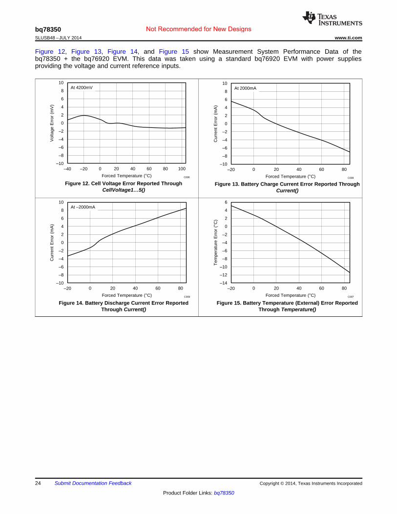
Figure 12, Figure 13, Figure 14, and Figure 15 show Measurement System Performance Data of thebq78350 + the bq76920 EVM. This data was taken using a standard bq76920 EVM with power suppliesproviding the voltage and current reference inputs.
Figure 12. Cell Voltage Error Reported Through Figure 13. Battery Charge Current Error Reported ThroughCellVoltage1…5() Current()
Figure 14. Battery Discharge Current Error Reported Figure 15. Battery Temperature (External) Error ReportedThrough Current() Through Temperature()
24 Submit Documentation Feedback Copyright © 2014, Texas Instruments Incorporated
Product Folder Links: bq78350
Not Recommended for New Designs
bq78350www.ti.com SLUSB48 –JULY 2014
11 Power Supply RecommendationsThe bq78350 is powered directly from the 2.5-V REGOUT pin of the bq769x0 companion AFE. An inputcapacitor of 0.1 µF is required between VCC and VSS and should be placed as close to the bq78350 aspossible.
To ensure correct power up of the bq78350, a 100-k resistor between MRST and VCC is also required. See theschematic for further details.
Copyright © 2014, Texas Instruments Incorporated Submit Documentation Feedback 25
Product Folder Links: bq78350
Not Recommended for New Designs
bq78350SLUSB48 –JULY 2014 www.ti.com
12 Layout
12.1 Layout Guidelines
12.1.1 Power Supply Decoupling CapacitorPower supply decoupling from VCC to ground is important for optimal operation of the bq78350. To keep theloop area small, place this capacitor next to the IC and use the shortest possible traces. A large-loop arearenders the capacitor useless and forms a small-loop antenna for noise pickup.
Ideally, the traces on each side of the capacitor must be the same length and run in the same direction to avoiddifferential noise during ESD. If possible, place a via near the VSS pin to a ground plane layer.
Placement of the RBI capacitor is not as critical. It can be placed further away from the IC.
12.1.2 MRST ConnectionThe MRST pin controls the gas gauge reset state. The connections to this pin must be as short as possible inorder to avoid any incoming noise. Direct connection to VCC is possible if the reset functionality is not desired ornecessary.
If unwanted resets are found, one or more of the following solutions may be effective:• Add a 0.1-μF capacitor between MRST and ground.• Provide a 1-kΩ pull up resistor to VCC at MRST.• Surround the entire circuit with a ground pattern.
If a test point is added at MRST, it must be provided with a 10-kΩ series resistor.
12.1.3 Communication Line Protection ComponentsThe 5.6-V Zener diodes, which protect the bq78350 communication pins from ESD, must be located as close aspossible to the pack connector. The grounded end of these Zener diodes must be returned to the PACK(–) node,rather than to the low-current digital ground system. This way, ESD is diverted away from the sensitiveelectronics as much as possible.
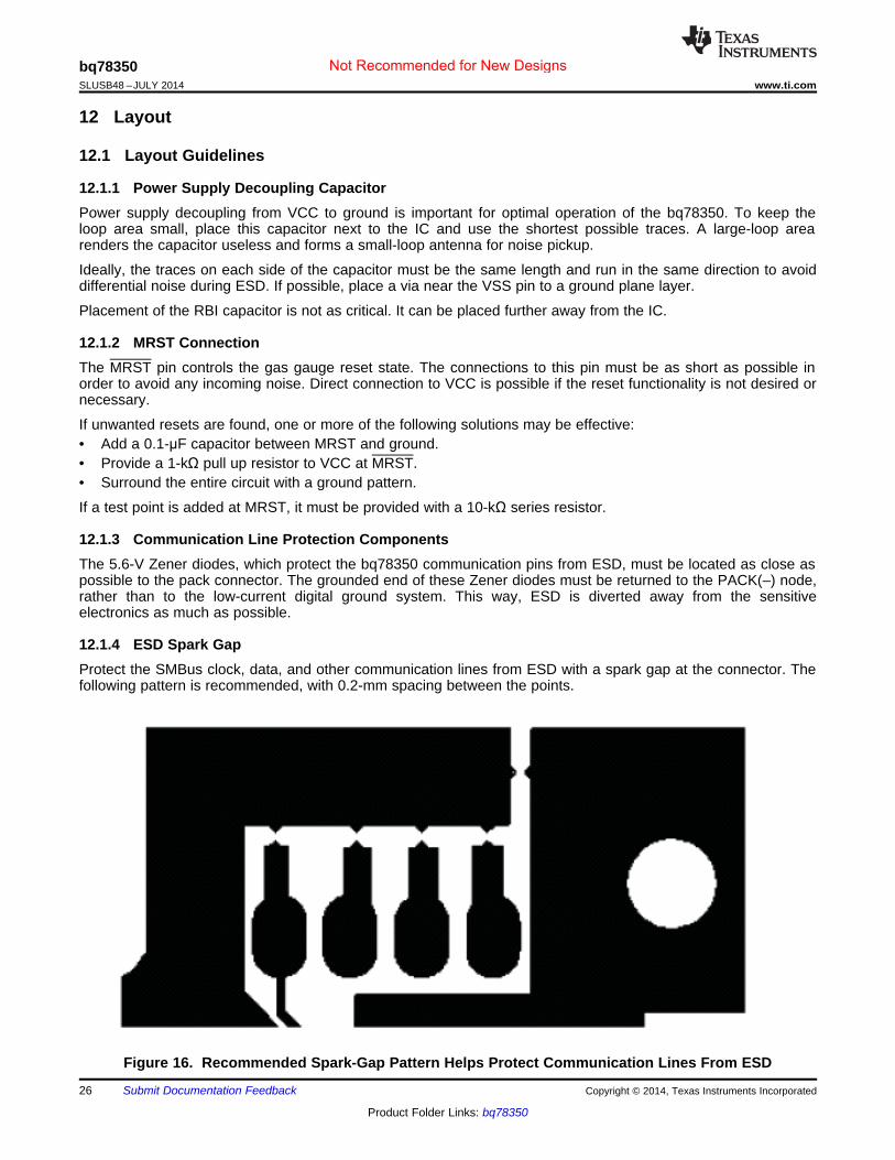
12.1.4 ESD Spark GapProtect the SMBus clock, data, and other communication lines from ESD with a spark gap at the connector. Thefollowing pattern is recommended, with 0.2-mm spacing between the points.
Figure 16. Recommended Spark-Gap Pattern Helps Protect Communication Lines From ESD
26 Submit Documentation Feedback Copyright © 2014, Texas Instruments Incorporated
Product Folder Links: bq78350
Not Recommended for New Designs
VCC
bq78350
C22C21
RBI
bq78350www.ti.com SLUSB48 –JULY 2014
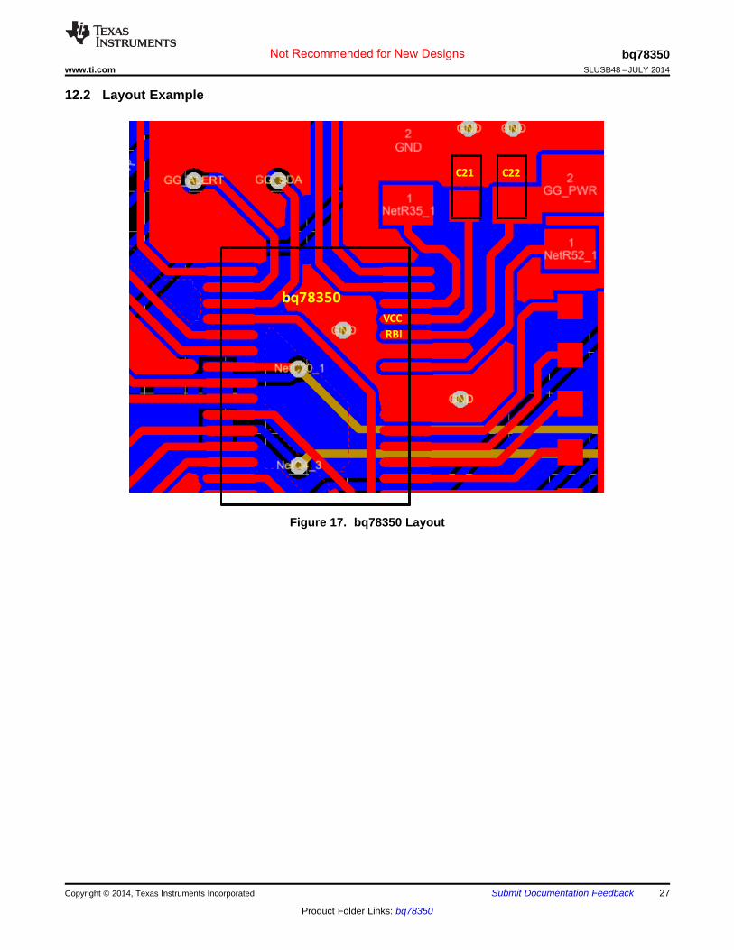
12.2 Layout Example
Figure 17. bq78350 Layout
Copyright © 2014, Texas Instruments Incorporated Submit Documentation Feedback 27
Product Folder Links: bq78350
Not Recommended for New Designs
bq78350SLUSB48 –JULY 2014 www.ti.com
13 Device and Documentation Support
13.1 Related DocumentationFor related documentation, see the following:• bq78350 Technical Reference Manual (SLUUAN7)• Using the bq78350 Application Note (SLUA726)• bq769x0 3-Series to 15-Series Cell Battery Monitor Family for Li-Ion and Phosphate Applications Data
Manual (SLUSBK2)
13.2 TrademarksAll trademarks are the property of their respective owners.
13.3 Electrostatic Discharge CautionThis integrated circuit can be damaged by ESD. Texas Instruments recommends that all integrated circuits be handled withappropriate precautions. Failure to observe proper handling and installation procedures can cause damage.
ESD damage can range from subtle performance degradation to complete device failure. Precision integrated circuits may be moresusceptible to damage because very small parametric changes could cause the device not to meet its published specifications.
13.4 GlossarySLYZ022 — TI Glossary.
This glossary lists and explains terms, acronyms, and definitions.
14 Mechanical, Packaging, and Orderable InformationThe following pages include mechanical, packaging, and orderable information. This information is the mostcurrent data available for the designated devices. This data is subject to change without notice and revision ofthis document. For browser-based versions of this data sheet, refer to the left-hand navigation.
28 Submit Documentation Feedback Copyright © 2014, Texas Instruments Incorporated
Product Folder Links: bq78350
Not Recommended for New Designs
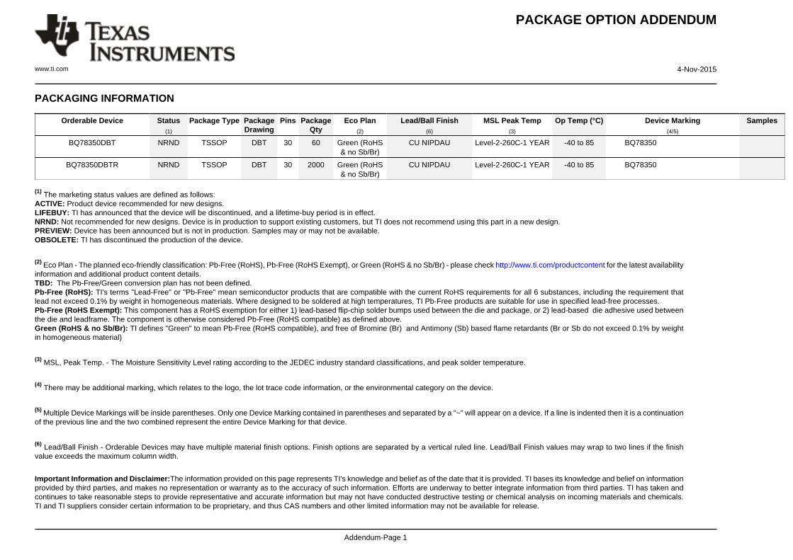
PACKAGE OPTION ADDENDUM
www.ti.com 4-Nov-2015
Addendum-Page 1
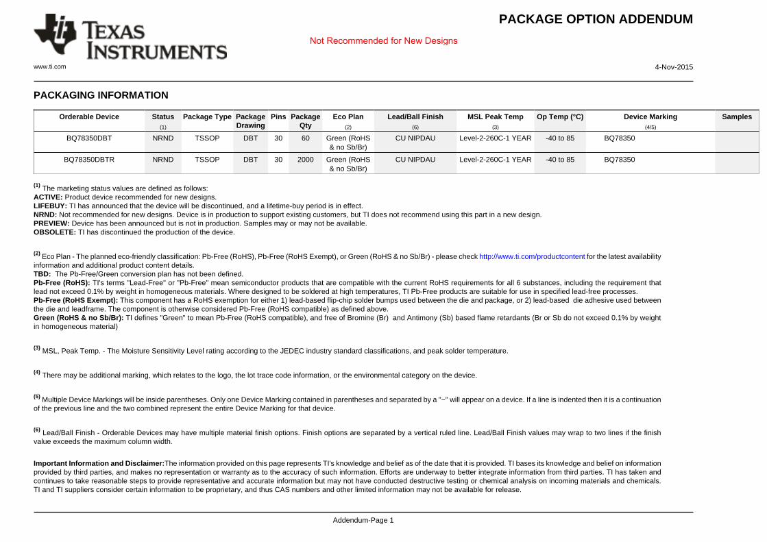
PACKAGING INFORMATION
Orderable Device Status(1)
Package Type PackageDrawing
Pins PackageQty
Eco Plan(2)
Lead/Ball Finish(6)
MSL Peak Temp(3)
Op Temp (°C) Device Marking(4/5)
Samples
BQ78350DBT NRND TSSOP DBT 30 60 Green (RoHS& no Sb/Br)
CU NIPDAU Level-2-260C-1 YEAR -40 to 85 BQ78350
BQ78350DBTR NRND TSSOP DBT 30 2000 Green (RoHS& no Sb/Br)
CU NIPDAU Level-2-260C-1 YEAR -40 to 85 BQ78350
(1) The marketing status values are defined as follows:ACTIVE: Product device recommended for new designs.LIFEBUY: TI has announced that the device will be discontinued, and a lifetime-buy period is in effect.NRND: Not recommended for new designs. Device is in production to support existing customers, but TI does not recommend using this part in a new design.PREVIEW: Device has been announced but is not in production. Samples may or may not be available.OBSOLETE: TI has discontinued the production of the device.
(2) Eco Plan - The planned eco-friendly classification: Pb-Free (RoHS), Pb-Free (RoHS Exempt), or Green (RoHS & no Sb/Br) - please check http://www.ti.com/productcontent for the latest availabilityinformation and additional product content details.TBD: The Pb-Free/Green conversion plan has not been defined.Pb-Free (RoHS): TI's terms "Lead-Free" or "Pb-Free" mean semiconductor products that are compatible with the current RoHS requirements for all 6 substances, including the requirement thatlead not exceed 0.1% by weight in homogeneous materials. Where designed to be soldered at high temperatures, TI Pb-Free products are suitable for use in specified lead-free processes.Pb-Free (RoHS Exempt): This component has a RoHS exemption for either 1) lead-based flip-chip solder bumps used between the die and package, or 2) lead-based die adhesive used betweenthe die and leadframe. The component is otherwise considered Pb-Free (RoHS compatible) as defined above.Green (RoHS & no Sb/Br): TI defines "Green" to mean Pb-Free (RoHS compatible), and free of Bromine (Br) and Antimony (Sb) based flame retardants (Br or Sb do not exceed 0.1% by weightin homogeneous material)
(3) MSL, Peak Temp. - The Moisture Sensitivity Level rating according to the JEDEC industry standard classifications, and peak solder temperature.
(4) There may be additional marking, which relates to the logo, the lot trace code information, or the environmental category on the device.
(5) Multiple Device Markings will be inside parentheses. Only one Device Marking contained in parentheses and separated by a "~" will appear on a device. If a line is indented then it is a continuationof the previous line and the two combined represent the entire Device Marking for that device.
(6) Lead/Ball Finish - Orderable Devices may have multiple material finish options. Finish options are separated by a vertical ruled line. Lead/Ball Finish values may wrap to two lines if the finishvalue exceeds the maximum column width.
Important Information and Disclaimer:The information provided on this page represents TI's knowledge and belief as of the date that it is provided. TI bases its knowledge and belief on informationprovided by third parties, and makes no representation or warranty as to the accuracy of such information. Efforts are underway to better integrate information from third parties. TI has taken andcontinues to take reasonable steps to provide representative and accurate information but may not have conducted destructive testing or chemical analysis on incoming materials and chemicals.TI and TI suppliers consider certain information to be proprietary, and thus CAS numbers and other limited information may not be available for release.
Not Recommended for New Designs
PACKAGE OPTION ADDENDUM
www.ti.com 4-Nov-2015
Addendum-Page 2
In no event shall TI's liability arising out of such information exceed the total purchase price of the TI part(s) at issue in this document sold by TI to Customer on an annual basis.
Not Recommended for New Designs
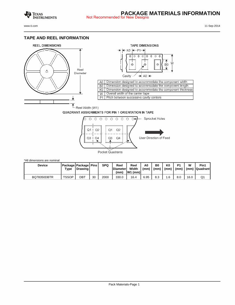
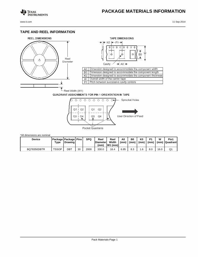
TAPE AND REEL INFORMATION
*All dimensions are nominal
Device PackageType
PackageDrawing
Pins SPQ ReelDiameter
(mm)
ReelWidth
W1 (mm)
A0(mm)
B0(mm)
K0(mm)
P1(mm)
W(mm)
Pin1Quadrant
BQ78350DBTR TSSOP DBT 30 2000 330.0 16.4 6.95 8.3 1.6 8.0 16.0 Q1
PACKAGE MATERIALS INFORMATION
www.ti.com 11-Sep-2014
Pack Materials-Page 1
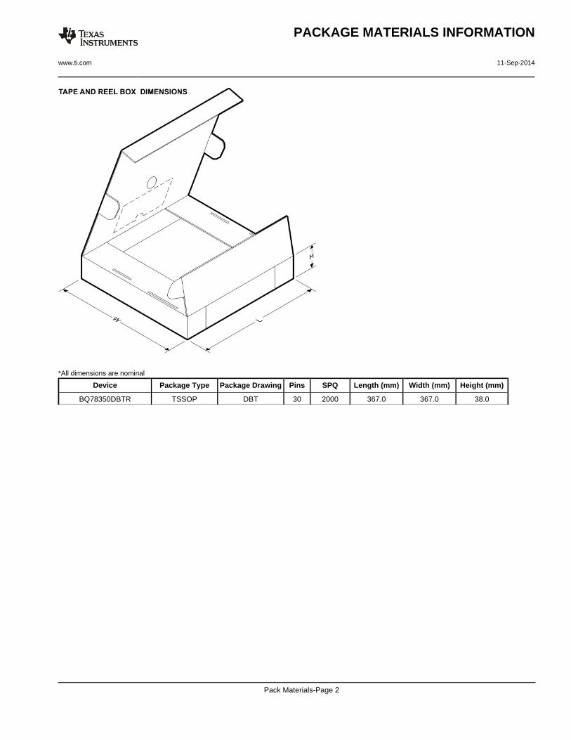
Not Recommended for New Designs
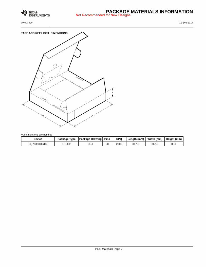
*All dimensions are nominal
Device Package Type Package Drawing Pins SPQ Length (mm) Width (mm) Height (mm)
BQ78350DBTR TSSOP DBT 30 2000 367.0 367.0 38.0
PACKAGE MATERIALS INFORMATION
www.ti.com 11-Sep-2014
Pack Materials-Page 2
Not Recommended for New Designs
Not Recommended for New Designs
PACKAGE OPTION ADDENDUM
www.ti.com 4-Nov-2015
Addendum-Page 1
PACKAGING INFORMATION
Orderable Device Status(1)
Package Type PackageDrawing
Pins PackageQty
Eco Plan(2)
Lead/Ball Finish(6)
MSL Peak Temp(3)
Op Temp (°C) Device Marking(4/5)
Samples
BQ78350DBT NRND TSSOP DBT 30 60 Green (RoHS& no Sb/Br)
CU NIPDAU Level-2-260C-1 YEAR -40 to 85 BQ78350
BQ78350DBTR NRND TSSOP DBT 30 2000 Green (RoHS& no Sb/Br)
CU NIPDAU Level-2-260C-1 YEAR -40 to 85 BQ78350
(1) The marketing status values are defined as follows:ACTIVE: Product device recommended for new designs.LIFEBUY: TI has announced that the device will be discontinued, and a lifetime-buy period is in effect.NRND: Not recommended for new designs. Device is in production to support existing customers, but TI does not recommend using this part in a new design.PREVIEW: Device has been announced but is not in production. Samples may or may not be available.OBSOLETE: TI has discontinued the production of the device.
(2) Eco Plan - The planned eco-friendly classification: Pb-Free (RoHS), Pb-Free (RoHS Exempt), or Green (RoHS & no Sb/Br) - please check http://www.ti.com/productcontent for the latest availabilityinformation and additional product content details.TBD: The Pb-Free/Green conversion plan has not been defined.Pb-Free (RoHS): TI's terms "Lead-Free" or "Pb-Free" mean semiconductor products that are compatible with the current RoHS requirements for all 6 substances, including the requirement thatlead not exceed 0.1% by weight in homogeneous materials. Where designed to be soldered at high temperatures, TI Pb-Free products are suitable for use in specified lead-free processes.Pb-Free (RoHS Exempt): This component has a RoHS exemption for either 1) lead-based flip-chip solder bumps used between the die and package, or 2) lead-based die adhesive used betweenthe die and leadframe. The component is otherwise considered Pb-Free (RoHS compatible) as defined above.Green (RoHS & no Sb/Br): TI defines "Green" to mean Pb-Free (RoHS compatible), and free of Bromine (Br) and Antimony (Sb) based flame retardants (Br or Sb do not exceed 0.1% by weightin homogeneous material)
(3) MSL, Peak Temp. - The Moisture Sensitivity Level rating according to the JEDEC industry standard classifications, and peak solder temperature.
(4) There may be additional marking, which relates to the logo, the lot trace code information, or the environmental category on the device.
(5) Multiple Device Markings will be inside parentheses. Only one Device Marking contained in parentheses and separated by a "~" will appear on a device. If a line is indented then it is a continuationof the previous line and the two combined represent the entire Device Marking for that device.
(6) Lead/Ball Finish - Orderable Devices may have multiple material finish options. Finish options are separated by a vertical ruled line. Lead/Ball Finish values may wrap to two lines if the finishvalue exceeds the maximum column width.
Important Information and Disclaimer:The information provided on this page represents TI's knowledge and belief as of the date that it is provided. TI bases its knowledge and belief on informationprovided by third parties, and makes no representation or warranty as to the accuracy of such information. Efforts are underway to better integrate information from third parties. TI has taken andcontinues to take reasonable steps to provide representative and accurate information but may not have conducted destructive testing or chemical analysis on incoming materials and chemicals.TI and TI suppliers consider certain information to be proprietary, and thus CAS numbers and other limited information may not be available for release.
PACKAGE OPTION ADDENDUM
www.ti.com 4-Nov-2015
Addendum-Page 2
In no event shall TI's liability arising out of such information exceed the total purchase price of the TI part(s) at issue in this document sold by TI to Customer on an annual basis.
TAPE AND REEL INFORMATION
*All dimensions are nominal
Device PackageType
PackageDrawing
Pins SPQ ReelDiameter
(mm)
ReelWidth
W1 (mm)
A0(mm)
B0(mm)
K0(mm)
P1(mm)
W(mm)
Pin1Quadrant
BQ78350DBTR TSSOP DBT 30 2000 330.0 16.4 6.95 8.3 1.6 8.0 16.0 Q1
PACKAGE MATERIALS INFORMATION
www.ti.com 11-Sep-2014
Pack Materials-Page 1
*All dimensions are nominal
Device Package Type Package Drawing Pins SPQ Length (mm) Width (mm) Height (mm)
BQ78350DBTR TSSOP DBT 30 2000 367.0 367.0 38.0
PACKAGE MATERIALS INFORMATION
www.ti.com 11-Sep-2014
Pack Materials-Page 2
IMPORTANT NOTICE
Texas Instruments Incorporated and its subsidiaries (TI) reserve the right to make corrections, enhancements, improvements and otherchanges to its semiconductor products and services per JESD46, latest issue, and to discontinue any product or service per JESD48, latestissue. Buyers should obtain the latest relevant information before placing orders and should verify that such information is current andcomplete. All semiconductor products (also referred to herein as “components”) are sold subject to TI’s terms and conditions of salesupplied at the time of order acknowledgment.TI warrants performance of its components to the specifications applicable at the time of sale, in accordance with the warranty in TI’s termsand conditions of sale of semiconductor products. Testing and other quality control techniques are used to the extent TI deems necessaryto support this warranty. Except where mandated by applicable law, testing of all parameters of each component is not necessarilyperformed.TI assumes no liability for applications assistance or the design of Buyers’ products. Buyers are responsible for their products andapplications using TI components. To minimize the risks associated with Buyers’ products and applications, Buyers should provideadequate design and operating safeguards.TI does not warrant or represent that any license, either express or implied, is granted under any patent right, copyright, mask work right, orother intellectual property right relating to any combination, machine, or process in which TI components or services are used. Informationpublished by TI regarding third-party products or services does not constitute a license to use such products or services or a warranty orendorsement thereof. Use of such information may require a license from a third party under the patents or other intellectual property of thethird party, or a license from TI under the patents or other intellectual property of TI.Reproduction of significant portions of TI information in TI data books or data sheets is permissible only if reproduction is without alterationand is accompanied by all associated warranties, conditions, limitations, and notices. TI is not responsible or liable for such altereddocumentation. Information of third parties may be subject to additional restrictions.Resale of TI components or services with statements different from or beyond the parameters stated by TI for that component or servicevoids all express and any implied warranties for the associated TI component or service and is an unfair and deceptive business practice.TI is not responsible or liable for any such statements.Buyer acknowledges and agrees that it is solely responsible for compliance with all legal, regulatory and safety-related requirementsconcerning its products, and any use of TI components in its applications, notwithstanding any applications-related information or supportthat may be provided by TI. Buyer represents and agrees that it has all the necessary expertise to create and implement safeguards whichanticipate dangerous consequences of failures, monitor failures and their consequences, lessen the likelihood of failures that might causeharm and take appropriate remedial actions. Buyer will fully indemnify TI and its representatives against any damages arising out of the useof any TI components in safety-critical applications.In some cases, TI components may be promoted specifically to facilitate safety-related applications. With such components, TI’s goal is tohelp enable customers to design and create their own end-product solutions that meet applicable functional safety standards andrequirements. Nonetheless, such components are subject to these terms.No TI components are authorized for use in FDA Class III (or similar life-critical medical equipment) unless authorized officers of the partieshave executed a special agreement specifically governing such use.Only those TI components which TI has specifically designated as military grade or “enhanced plastic” are designed and intended for use inmilitary/aerospace applications or environments. Buyer acknowledges and agrees that any military or aerospace use of TI componentswhich have not been so designated is solely at the Buyer's risk, and that Buyer is solely responsible for compliance with all legal andregulatory requirements in connection with such use.TI has specifically designated certain components as meeting ISO/TS16949 requirements, mainly for automotive use. In any case of use ofnon-designated products, TI will not be responsible for any failure to meet ISO/TS16949.
Products ApplicationsAudio www.ti.com/audio Automotive and Transportation www.ti.com/automotiveAmplifiers amplifier.ti.com Communications and Telecom www.ti.com/communicationsData Converters dataconverter.ti.com Computers and Peripherals www.ti.com/computersDLP® Products www.dlp.com Consumer Electronics www.ti.com/consumer-appsDSP dsp.ti.com Energy and Lighting www.ti.com/energyClocks and Timers www.ti.com/clocks Industrial www.ti.com/industrialInterface interface.ti.com Medical www.ti.com/medicalLogic logic.ti.com Security www.ti.com/securityPower Mgmt power.ti.com Space, Avionics and Defense www.ti.com/space-avionics-defenseMicrocontrollers microcontroller.ti.com Video and Imaging www.ti.com/videoRFID www.ti-rfid.comOMAP Applications Processors www.ti.com/omap TI E2E Community e2e.ti.comWireless Connectivity www.ti.com/wirelessconnectivity
Mailing Address: Texas Instruments, Post Office Box 655303, Dallas, Texas 75265Copyright © 2016, Texas Instruments Incorporated


![NBS TECHNICAL NOTE 692 · 2002. 8. 16. · w,) + B COS ntI2 + kl[(wl - a,) + B COS Qt] where y = 2nW relates to the linewidth, w is the instantaneous angular frequency of the VC0,wl](https://img.dokumen.tips/doc/110x75/61320d26dfd10f4dd73a3283/nbs-technical-note-692-2002-8-16-w-b-cos-nti2-klwl-a-b-cos-qt.jpg)


