Embed Size (px)
Citation preview

Journal of Physics Conference Series
OPEN ACCESS
Biexciton binding energy control in site-selectedquantum dotsTo cite this article M E Reimer et al 2010 J Phys Conf Ser 210 012019
View the article online for updates and enhancements
You may also likeNoble Metal Nanostructures Synthesizedinside Mesoporous Nanotemplate PoresJ Arbiol E Rossinyol A Cabot et al
-
A HfO2 Thin Film Resistive Switch Basedon Conducting Atomic Force MicroscopyJ Y Son D-Y Kim H Kim et al
-
Fabrication of Ultrathin Nb Nanopin ArraysJong Yeog Son Yun-Sok Shin Young-Han Shin et al
-
This content was downloaded from IP address 67209201201 on 05022022 at 0358
Biexciton binding energy control in site-selected
quantum dots
M E Reimer12 D Dalacu1 P J Poole1 and R L Williams1
1 Institute for Microstructural Sciences National Research Council of Canada OttawaK1A 0R6 Canada2 Kavli Institute of Nanoscience Delft University of Technology PO Box 5046 2600 GADelft The Netherlands
E-mail mereimertudelftnl
Abstract A unique nanotemplate deposition technique is utilized in growth of semiconductorquantum dots which enables precise control over the dot dimensions and nucleation site Herewe demonstrate tuning of the biexciton binding energy in a single site-selected InAsInPquantum dot through manipulation of the nanotemplate dimensions and thus dot size Amonotonic decrease of the biexciton binding energy from the binding to anti-binding regimethrough zero is observed with increasing dot size Piezoelectric fields in large quantum dotsare suggested as the mechanism to obtain an unbound biexciton state The tunability of thebiexciton binding energy demonstrated here for a deterministically positioned quantum dot isan important step towards a scalable route in the generation of entangled photon pairs thatemit around the telecommunications band of 155 μm
1 IntroductionThe generation of entangled photon pairs in semiconductor quantum dots relies heavily on theremoval of the fine-structure splitting (FSS) of the intermediate exciton states in the biexciton-exciton radiative cascade [1] Recent proposals to circumvent this requirement and thus produceentangled photon pairs even in the presence of non-zero FSS include the following tuningof the biexciton binding energy to zero with a lateral electric field and time-reordering [2ndash5]modulation of the exciton and biexciton energy levels with a frequency corresponding to theFSS [6] and coupling of the biexciton and exciton transitions to cavity modes with orthogonalpolarizations [7] Until now experimental investigations of biexciton binding energy ΔXX on dot size have been performed on randomly located quantum dots [8ndash13] However in thiswork we demonstrate tuning of the biexciton binding energy by controlling the nanotemplatedimensions and thus dot size of a single site-selected InAsInP quantum dot In particular thenanotemplate dimensions control the lateral dot dimensions while the amount of dot materialdeposited controls the dot height and therefore exciton emission energy [14 15] Additionallythese results also investigate a new regime for the dependence of ΔXX on dot size in largerquantum dots that emit near the telecommunications band of 155μm a wavelength range ofinterest for applications in quantum cryptography Of particular importance is that ΔXX isfound to be directly influenced by the dimensions of the ridge nanotemplate Here ΔXX can betuned from the binding (bound) to antibinding (unbound) regime through zero ndash a regime notpreviously studied in large dots
International Conference on Optics of Excitons in Confined Systems (OECS11) IOP PublishingJournal of Physics Conference Series 210 (2010) 012019 doi1010881742-65962101012019
ccopy 2010 IOP Publishing Ltd 1
300nm
InP ridge
InAs dots (b)
300nm
SiO mask2
(c)
300nm
(a)
300nm 300nm 300nm
(d)InP pyramidInAs dot
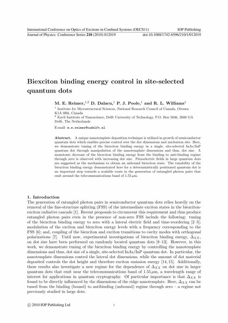
Figure 1 Plan view SEM images of uncapped ridge nanotemplates with varying base widthdimensions (a) 390 nm (b) 335 nm and (c) 325 nm The top (001) surface lateral dimensionsreduces with decreasing ridge base width until only a single row of quantum dots is obtainedin (c) (d) Control of single dot dimensions via square-based nanotemplate The base widthdimensions of the nanotemplate increase from left to right corresponding to an increase in dotsize
2 SampleSEM images of ridge nanotemplate structures of lsquostripersquo geometry with varying base widths w0produced under identical growth conditions are shown in Figure 1 Since the ridge nanotemplatesare subject to identical growth conditions larger starting base widths will result in a wider areaavailable for quantum dot growth If the ridge is sufficiently wide dots are randomly distributedon top of the ridge in a manner similar to that of conventionally grown dots on planar substratesas shown in Figure 1(a) As the top (001) surface w of the nanotemplate narrows the dotgrowth is affected in two ways First the top width of the nanotemplate confines the areaavailable for growth When lateral dimensions are significantly reduced the quantum dots willorder on the top apex as to minimize the strain The randomly distributed flat dots as shown inFigure 1(a) will transition to a double ordered dot array as shown in Figure 1(b) By reducingthe ridge base width further the lateral dimensions of the ridge (001) apex can only support asingle row of quantum dots as shown in Figure 1(c) The lateral dimensions of the dots shown inFigure 1(c) are approximately 30-40 nm Second the amount of dot material (InAs) deposited onthe top (001) surface is enhanced as the ratio of w0w increases This corresponds to an increasein the quantum dot height and dot emission shift towards the telecommunications wavelengthof 155μm [15] The increase in quantum dot height can be inferred by the enhanced contrastof the SEM images from Figures 1(a)-(c) To facilitate single dot isolation and application oflateral electric fields for entangled photon pair generation a pair of Schottky gates with narrow300 nm gaps are fabricated [2 3 16] Similar control of the dot dimensions can be achieved onthe single dot level as shown in Figure 1(d) Here the template geometry is modified to asquare-based nanotemplate
3 Identification of exciton and biexciton in experimentTo identify the exciton (X) and biexciton (XX) in experiment a combination of bothpower (state-filling spectroscopy) and polarization dependent spectroscopy of the observedphotoluminescence (PL) emission spectra was conducted similarly to previous studies [81112]Moreover electric field dependence can be used as an additional experimental tool to identifythe exciton and biexciton since Coulomb interactions play an important role [34] Consequentlythe exciton and biexciton exhibit unique signatures (ie Stark shifts fine-structure life time
International Conference on Optics of Excitons in Confined Systems (OECS11) IOP PublishingJournal of Physics Conference Series 210 (2010) 012019 doi1010881742-65962101012019
2
(a) Bound XX (b) Unbound XX
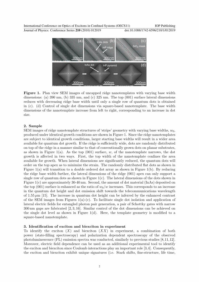
Figure 2 Typical state-shell filling spec-troscopy of (a) bound and (b) unboundbiexciton for a single prepositioned quan-tum dot on ridge nanotemplate at zero elec-tric field In the lower panel are fits (solidlines) to the data within the random cap-ture model Evidence of exciton and biex-citon are inferred from the resulting linearand superlinear power dependence of inte-grated intensity on excitation power
etc) as a function of lateral electric field which allows the biexciton-exciton cascade to bedifferentiated from all other cascades including charged excitonic states [3 4]
Typical single dot PL for single site-selected InAsInP quantum dots as a function ofincreasing excitation power at zero electric field is shown in the upper panel of Figure 2 In Figure2(a) the observed biexciton peak is bound while in Figure 2(b) the biexciton is unbound Theseassignments of X and XX transitions are determined within the random capture model by fittingthe integrated intensity of the emission peaks as a function of excitation power [12] Within thissimple model the slope is proportional to one and two for X and XX respectively which allowsthe observed optical transitions (X and XX) to be readily determined [12] Excellent fits areobtained for both the bound and unbound biexciton cases as shown in the lower panel of Figure2 In addition the saturation of both X and XX observed in experiment is well described byPoissonnian statistics for increasing excitation power The assignment of X and XX observedin experiment is confirmed in independent studies by polarization dependent spectroscopy andtheir electric field dependence [2 3]
Consistent with literature ΔXX = EX minusEXX [81112] Here a bound (unbound) biexcitonhas a positive (negative) ΔXX and is found at lower (higher) energy than X The biexcitonbinding energy is a direct result of Coulomb interactions of the two electron-hole pairs buildingthe biexciton and correlations of higher lying states [4] The positive contributions to ΔXX arisesfrom e-h Coulomb attraction and correlation effects while the negative component comes fromthe Coulomb repulsion between carriers of the same type Thus an unbound biexciton can bemanifested in small dots from a weaker dependence on electron-hole Coulomb interactions thanelectron-electron and hole-hole Coulomb repulsion or when the number of bound states decreasesthus leading to a reduction in correlations [11] In contrast strain induced piezoelectric fields inlarge dots can result in a separation of charges thus leading to an unbound biexciton state [913]
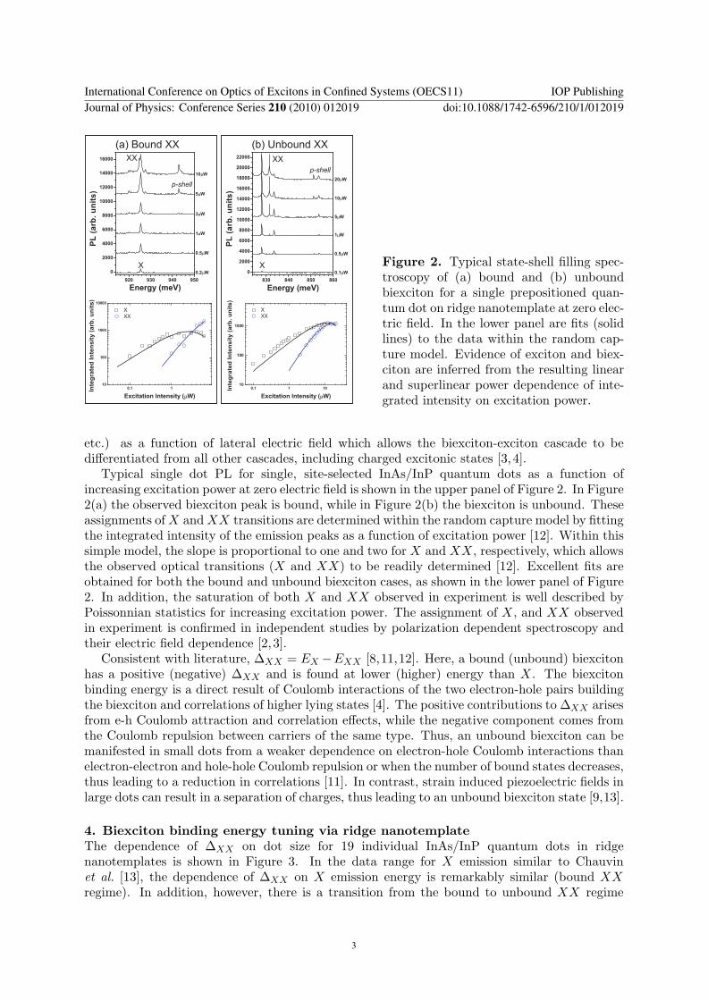
4 Biexciton binding energy tuning via ridge nanotemplateThe dependence of ΔXX on dot size for 19 individual InAsInP quantum dots in ridgenanotemplates is shown in Figure 3 In the data range for X emission similar to Chauvinet al [13] the dependence of ΔXX on X emission energy is remarkably similar (bound XXregime) In addition however there is a transition from the bound to unbound XX regime
International Conference on Optics of Excitons in Confined Systems (OECS11) IOP PublishingJournal of Physics Conference Series 210 (2010) 012019 doi1010881742-65962101012019
3
for decreasing X emission energy The tuning range controlled via the ridge nanotemplate israther large ΔXX = +31meV at X emission energy of 1011meV while ΔXX minus4meVnear the telecommunications wavelength of 155μm (800 meV) This corresponds to a controlledtuning range for ΔXX of 71meV The observed crossover point for zero XX binding energy (ieΔXX = 0) occurs in the energy range between sim 910 minus 930meV The resulting dependence ofΔXX on dot size is attributed to increases in piezoelectric fields with increasing dot size [913]Piezoelectric fields tend to separate charges which lead to an unbound XX state [9] howeverthe antibinding regime has not been achieved yet in large quantum dots until this work Theantibinding regime for XX in large dots may be a very important step towards the realizationof a scalable route for the generation of entangled photon pairs The piezoelectric fieldsthat produce a separation of charges leading to an antibinding XX state may also reducethe fine-structure splitting near zero since this splitting depends strongly on the electron-holewavefunction overlap [317] Indeed in the work of Chauvin et al no FSS was observed withinthe spectral resolution of 100μeV for large dots [13] Similar results were obtained for the dotsexhibiting an unbound XX state studied here within the spectral resolution of 50μeV (data notshown)
Figure 3 Controlled tunability of biexciton binding energyΔXX on dot size for ridge nanotemplate Decreasing theridge base width increases the dot height for the same amountof dot material deposited and shifts the the excition emissionenergy towards the telecommunications band around 155μm(800meV) while reducing ΔXX The scatter of ΔXX fora given exciton emission energy is due to variations in thelateral dot dimensions for a given quantum dot height
5 SummaryThe controlled tunability of ΔXX via the ridge nanotemplate presented here for individualInAsInP quantum dots is desirable for the realization of a scalable route to producing entangledphoton pair sources With appropriate choice of the growth conditions ΔXX can be engineeredto zero In cases where there are small deviations from ΔXX = 0 a lateral electric field can beused to remove the biexciton binding energy [2 3]
AcknowledgmentsThe authors would like to acknowledge the financial support of the Natural Sciences andEngineering Research Council QuantumWorks and the Business Development Bank of Canada
References[1] Stevenson R M Young R J Atkinson P Cooper K Ritchie D A and Shields A J 2006 Nature 439 179ndash182[2] Reimer M E et al 2007 Voltage induced hidden symmetry and photon entanglement generation in a single
site-selected quantum dot (Preprint arXiv07061075)[3] Reimer M E Korkusinski M Dalacu D Lefebvre J Lapointe J Poole P J Aers G C McKinnon W R
Hawrylak P and Williams R L 2008 Phys Rev B 78 195301[4] Korkusinski M Reimer M E Williams R L and Hawrylak P 2009 Phys Rev B 79 035309[5] Avron J E Bisker G Gershoni D Lindner N H Meirom E A and Warburton R J 2008 Phys Rev Lett 100
120501[6] Coish W A and Gambetta J M 2009 Sideband eraser of lsquowhich-pathrsquo information for entangled photons on
demand (Preprint arXiv09070437)[7] Pathak P K and Hughes S 2009 Phys Rev B 79 205416
International Conference on Optics of Excitons in Confined Systems (OECS11) IOP PublishingJournal of Physics Conference Series 210 (2010) 012019 doi1010881742-65962101012019
4
[8] Rodt S Heitz R Schliwa A Sellin R L Guffarth F and Bimberg D 2003 Phys Rev B 68 035331[9] Rodt S Schliwa A Potschke K Guffarth F and Bimberg D 2005 Phys Rev B 71 155325
[10] Seguin R Schliwa A Rodt S Potschke K Pohl U W and Bimberg D 2005 Phys Rev Lett 95 257402[11] Sarkar D van der Meulen H P Calleja J M Becker J M Haug R J and Pierz K 2006 Journal of Applied
Physics 100 023109[12] Savio C D Pierz K Ade G Danzebrink H U Gobel E and Hangleiter A 2006 Applied Physics B Lasers and
Optics 84 317ndash322[13] Chauvin N Salem B Bremond G Guillot G Bru-Chevallier C and Gendry M 2006 Journal of Applied
Physics 100 073702[14] Lefebvre J Poole P J Fraser J Aers G C Chithrani D and Williams R L 2002 J Cyrstal Growth 234
391ndash398[15] Lefebvre J Poole P J Aers G C Chithrani D and Williams R L 2002 J Vac Sci Technol B 20 2173ndash2176[16] Reimer M E et al 2008 Physica E Low-dimensional Systems and Nanostructures 40 1790ndash1793[17] Bayer M et al 2002 Phys Rev B 65 195315
International Conference on Optics of Excitons in Confined Systems (OECS11) IOP PublishingJournal of Physics Conference Series 210 (2010) 012019 doi1010881742-65962101012019
5
Biexciton binding energy control in site-selected
quantum dots
M E Reimer12 D Dalacu1 P J Poole1 and R L Williams1
1 Institute for Microstructural Sciences National Research Council of Canada OttawaK1A 0R6 Canada2 Kavli Institute of Nanoscience Delft University of Technology PO Box 5046 2600 GADelft The Netherlands
E-mail mereimertudelftnl
Abstract A unique nanotemplate deposition technique is utilized in growth of semiconductorquantum dots which enables precise control over the dot dimensions and nucleation site Herewe demonstrate tuning of the biexciton binding energy in a single site-selected InAsInPquantum dot through manipulation of the nanotemplate dimensions and thus dot size Amonotonic decrease of the biexciton binding energy from the binding to anti-binding regimethrough zero is observed with increasing dot size Piezoelectric fields in large quantum dotsare suggested as the mechanism to obtain an unbound biexciton state The tunability of thebiexciton binding energy demonstrated here for a deterministically positioned quantum dot isan important step towards a scalable route in the generation of entangled photon pairs thatemit around the telecommunications band of 155 μm
1 IntroductionThe generation of entangled photon pairs in semiconductor quantum dots relies heavily on theremoval of the fine-structure splitting (FSS) of the intermediate exciton states in the biexciton-exciton radiative cascade [1] Recent proposals to circumvent this requirement and thus produceentangled photon pairs even in the presence of non-zero FSS include the following tuningof the biexciton binding energy to zero with a lateral electric field and time-reordering [2ndash5]modulation of the exciton and biexciton energy levels with a frequency corresponding to theFSS [6] and coupling of the biexciton and exciton transitions to cavity modes with orthogonalpolarizations [7] Until now experimental investigations of biexciton binding energy ΔXX on dot size have been performed on randomly located quantum dots [8ndash13] However in thiswork we demonstrate tuning of the biexciton binding energy by controlling the nanotemplatedimensions and thus dot size of a single site-selected InAsInP quantum dot In particular thenanotemplate dimensions control the lateral dot dimensions while the amount of dot materialdeposited controls the dot height and therefore exciton emission energy [14 15] Additionallythese results also investigate a new regime for the dependence of ΔXX on dot size in largerquantum dots that emit near the telecommunications band of 155μm a wavelength range ofinterest for applications in quantum cryptography Of particular importance is that ΔXX isfound to be directly influenced by the dimensions of the ridge nanotemplate Here ΔXX can betuned from the binding (bound) to antibinding (unbound) regime through zero ndash a regime notpreviously studied in large dots
International Conference on Optics of Excitons in Confined Systems (OECS11) IOP PublishingJournal of Physics Conference Series 210 (2010) 012019 doi1010881742-65962101012019
ccopy 2010 IOP Publishing Ltd 1
300nm
InP ridge
InAs dots (b)
300nm
SiO mask2
(c)
300nm
(a)
300nm 300nm 300nm
(d)InP pyramidInAs dot
Figure 1 Plan view SEM images of uncapped ridge nanotemplates with varying base widthdimensions (a) 390 nm (b) 335 nm and (c) 325 nm The top (001) surface lateral dimensionsreduces with decreasing ridge base width until only a single row of quantum dots is obtainedin (c) (d) Control of single dot dimensions via square-based nanotemplate The base widthdimensions of the nanotemplate increase from left to right corresponding to an increase in dotsize
2 SampleSEM images of ridge nanotemplate structures of lsquostripersquo geometry with varying base widths w0produced under identical growth conditions are shown in Figure 1 Since the ridge nanotemplatesare subject to identical growth conditions larger starting base widths will result in a wider areaavailable for quantum dot growth If the ridge is sufficiently wide dots are randomly distributedon top of the ridge in a manner similar to that of conventionally grown dots on planar substratesas shown in Figure 1(a) As the top (001) surface w of the nanotemplate narrows the dotgrowth is affected in two ways First the top width of the nanotemplate confines the areaavailable for growth When lateral dimensions are significantly reduced the quantum dots willorder on the top apex as to minimize the strain The randomly distributed flat dots as shown inFigure 1(a) will transition to a double ordered dot array as shown in Figure 1(b) By reducingthe ridge base width further the lateral dimensions of the ridge (001) apex can only support asingle row of quantum dots as shown in Figure 1(c) The lateral dimensions of the dots shown inFigure 1(c) are approximately 30-40 nm Second the amount of dot material (InAs) deposited onthe top (001) surface is enhanced as the ratio of w0w increases This corresponds to an increasein the quantum dot height and dot emission shift towards the telecommunications wavelengthof 155μm [15] The increase in quantum dot height can be inferred by the enhanced contrastof the SEM images from Figures 1(a)-(c) To facilitate single dot isolation and application oflateral electric fields for entangled photon pair generation a pair of Schottky gates with narrow300 nm gaps are fabricated [2 3 16] Similar control of the dot dimensions can be achieved onthe single dot level as shown in Figure 1(d) Here the template geometry is modified to asquare-based nanotemplate
3 Identification of exciton and biexciton in experimentTo identify the exciton (X) and biexciton (XX) in experiment a combination of bothpower (state-filling spectroscopy) and polarization dependent spectroscopy of the observedphotoluminescence (PL) emission spectra was conducted similarly to previous studies [81112]Moreover electric field dependence can be used as an additional experimental tool to identifythe exciton and biexciton since Coulomb interactions play an important role [34] Consequentlythe exciton and biexciton exhibit unique signatures (ie Stark shifts fine-structure life time
International Conference on Optics of Excitons in Confined Systems (OECS11) IOP PublishingJournal of Physics Conference Series 210 (2010) 012019 doi1010881742-65962101012019
2
(a) Bound XX (b) Unbound XX
Figure 2 Typical state-shell filling spec-troscopy of (a) bound and (b) unboundbiexciton for a single prepositioned quan-tum dot on ridge nanotemplate at zero elec-tric field In the lower panel are fits (solidlines) to the data within the random cap-ture model Evidence of exciton and biex-citon are inferred from the resulting linearand superlinear power dependence of inte-grated intensity on excitation power
etc) as a function of lateral electric field which allows the biexciton-exciton cascade to bedifferentiated from all other cascades including charged excitonic states [3 4]
Typical single dot PL for single site-selected InAsInP quantum dots as a function ofincreasing excitation power at zero electric field is shown in the upper panel of Figure 2 In Figure2(a) the observed biexciton peak is bound while in Figure 2(b) the biexciton is unbound Theseassignments of X and XX transitions are determined within the random capture model by fittingthe integrated intensity of the emission peaks as a function of excitation power [12] Within thissimple model the slope is proportional to one and two for X and XX respectively which allowsthe observed optical transitions (X and XX) to be readily determined [12] Excellent fits areobtained for both the bound and unbound biexciton cases as shown in the lower panel of Figure2 In addition the saturation of both X and XX observed in experiment is well described byPoissonnian statistics for increasing excitation power The assignment of X and XX observedin experiment is confirmed in independent studies by polarization dependent spectroscopy andtheir electric field dependence [2 3]
Consistent with literature ΔXX = EX minusEXX [81112] Here a bound (unbound) biexcitonhas a positive (negative) ΔXX and is found at lower (higher) energy than X The biexcitonbinding energy is a direct result of Coulomb interactions of the two electron-hole pairs buildingthe biexciton and correlations of higher lying states [4] The positive contributions to ΔXX arisesfrom e-h Coulomb attraction and correlation effects while the negative component comes fromthe Coulomb repulsion between carriers of the same type Thus an unbound biexciton can bemanifested in small dots from a weaker dependence on electron-hole Coulomb interactions thanelectron-electron and hole-hole Coulomb repulsion or when the number of bound states decreasesthus leading to a reduction in correlations [11] In contrast strain induced piezoelectric fields inlarge dots can result in a separation of charges thus leading to an unbound biexciton state [913]
4 Biexciton binding energy tuning via ridge nanotemplateThe dependence of ΔXX on dot size for 19 individual InAsInP quantum dots in ridgenanotemplates is shown in Figure 3 In the data range for X emission similar to Chauvinet al [13] the dependence of ΔXX on X emission energy is remarkably similar (bound XXregime) In addition however there is a transition from the bound to unbound XX regime
International Conference on Optics of Excitons in Confined Systems (OECS11) IOP PublishingJournal of Physics Conference Series 210 (2010) 012019 doi1010881742-65962101012019
3
for decreasing X emission energy The tuning range controlled via the ridge nanotemplate israther large ΔXX = +31meV at X emission energy of 1011meV while ΔXX minus4meVnear the telecommunications wavelength of 155μm (800 meV) This corresponds to a controlledtuning range for ΔXX of 71meV The observed crossover point for zero XX binding energy (ieΔXX = 0) occurs in the energy range between sim 910 minus 930meV The resulting dependence ofΔXX on dot size is attributed to increases in piezoelectric fields with increasing dot size [913]Piezoelectric fields tend to separate charges which lead to an unbound XX state [9] howeverthe antibinding regime has not been achieved yet in large quantum dots until this work Theantibinding regime for XX in large dots may be a very important step towards the realizationof a scalable route for the generation of entangled photon pairs The piezoelectric fieldsthat produce a separation of charges leading to an antibinding XX state may also reducethe fine-structure splitting near zero since this splitting depends strongly on the electron-holewavefunction overlap [317] Indeed in the work of Chauvin et al no FSS was observed withinthe spectral resolution of 100μeV for large dots [13] Similar results were obtained for the dotsexhibiting an unbound XX state studied here within the spectral resolution of 50μeV (data notshown)
Figure 3 Controlled tunability of biexciton binding energyΔXX on dot size for ridge nanotemplate Decreasing theridge base width increases the dot height for the same amountof dot material deposited and shifts the the excition emissionenergy towards the telecommunications band around 155μm(800meV) while reducing ΔXX The scatter of ΔXX fora given exciton emission energy is due to variations in thelateral dot dimensions for a given quantum dot height
5 SummaryThe controlled tunability of ΔXX via the ridge nanotemplate presented here for individualInAsInP quantum dots is desirable for the realization of a scalable route to producing entangledphoton pair sources With appropriate choice of the growth conditions ΔXX can be engineeredto zero In cases where there are small deviations from ΔXX = 0 a lateral electric field can beused to remove the biexciton binding energy [2 3]
AcknowledgmentsThe authors would like to acknowledge the financial support of the Natural Sciences andEngineering Research Council QuantumWorks and the Business Development Bank of Canada
References[1] Stevenson R M Young R J Atkinson P Cooper K Ritchie D A and Shields A J 2006 Nature 439 179ndash182[2] Reimer M E et al 2007 Voltage induced hidden symmetry and photon entanglement generation in a single
site-selected quantum dot (Preprint arXiv07061075)[3] Reimer M E Korkusinski M Dalacu D Lefebvre J Lapointe J Poole P J Aers G C McKinnon W R
Hawrylak P and Williams R L 2008 Phys Rev B 78 195301[4] Korkusinski M Reimer M E Williams R L and Hawrylak P 2009 Phys Rev B 79 035309[5] Avron J E Bisker G Gershoni D Lindner N H Meirom E A and Warburton R J 2008 Phys Rev Lett 100
120501[6] Coish W A and Gambetta J M 2009 Sideband eraser of lsquowhich-pathrsquo information for entangled photons on
demand (Preprint arXiv09070437)[7] Pathak P K and Hughes S 2009 Phys Rev B 79 205416
International Conference on Optics of Excitons in Confined Systems (OECS11) IOP PublishingJournal of Physics Conference Series 210 (2010) 012019 doi1010881742-65962101012019
4
[8] Rodt S Heitz R Schliwa A Sellin R L Guffarth F and Bimberg D 2003 Phys Rev B 68 035331[9] Rodt S Schliwa A Potschke K Guffarth F and Bimberg D 2005 Phys Rev B 71 155325
[10] Seguin R Schliwa A Rodt S Potschke K Pohl U W and Bimberg D 2005 Phys Rev Lett 95 257402[11] Sarkar D van der Meulen H P Calleja J M Becker J M Haug R J and Pierz K 2006 Journal of Applied
Physics 100 023109[12] Savio C D Pierz K Ade G Danzebrink H U Gobel E and Hangleiter A 2006 Applied Physics B Lasers and
Optics 84 317ndash322[13] Chauvin N Salem B Bremond G Guillot G Bru-Chevallier C and Gendry M 2006 Journal of Applied
Physics 100 073702[14] Lefebvre J Poole P J Fraser J Aers G C Chithrani D and Williams R L 2002 J Cyrstal Growth 234
391ndash398[15] Lefebvre J Poole P J Aers G C Chithrani D and Williams R L 2002 J Vac Sci Technol B 20 2173ndash2176[16] Reimer M E et al 2008 Physica E Low-dimensional Systems and Nanostructures 40 1790ndash1793[17] Bayer M et al 2002 Phys Rev B 65 195315
International Conference on Optics of Excitons in Confined Systems (OECS11) IOP PublishingJournal of Physics Conference Series 210 (2010) 012019 doi1010881742-65962101012019
5
300nm
InP ridge
InAs dots (b)
300nm
SiO mask2
(c)
300nm
(a)
300nm 300nm 300nm
(d)InP pyramidInAs dot
Figure 1 Plan view SEM images of uncapped ridge nanotemplates with varying base widthdimensions (a) 390 nm (b) 335 nm and (c) 325 nm The top (001) surface lateral dimensionsreduces with decreasing ridge base width until only a single row of quantum dots is obtainedin (c) (d) Control of single dot dimensions via square-based nanotemplate The base widthdimensions of the nanotemplate increase from left to right corresponding to an increase in dotsize
2 SampleSEM images of ridge nanotemplate structures of lsquostripersquo geometry with varying base widths w0produced under identical growth conditions are shown in Figure 1 Since the ridge nanotemplatesare subject to identical growth conditions larger starting base widths will result in a wider areaavailable for quantum dot growth If the ridge is sufficiently wide dots are randomly distributedon top of the ridge in a manner similar to that of conventionally grown dots on planar substratesas shown in Figure 1(a) As the top (001) surface w of the nanotemplate narrows the dotgrowth is affected in two ways First the top width of the nanotemplate confines the areaavailable for growth When lateral dimensions are significantly reduced the quantum dots willorder on the top apex as to minimize the strain The randomly distributed flat dots as shown inFigure 1(a) will transition to a double ordered dot array as shown in Figure 1(b) By reducingthe ridge base width further the lateral dimensions of the ridge (001) apex can only support asingle row of quantum dots as shown in Figure 1(c) The lateral dimensions of the dots shown inFigure 1(c) are approximately 30-40 nm Second the amount of dot material (InAs) deposited onthe top (001) surface is enhanced as the ratio of w0w increases This corresponds to an increasein the quantum dot height and dot emission shift towards the telecommunications wavelengthof 155μm [15] The increase in quantum dot height can be inferred by the enhanced contrastof the SEM images from Figures 1(a)-(c) To facilitate single dot isolation and application oflateral electric fields for entangled photon pair generation a pair of Schottky gates with narrow300 nm gaps are fabricated [2 3 16] Similar control of the dot dimensions can be achieved onthe single dot level as shown in Figure 1(d) Here the template geometry is modified to asquare-based nanotemplate
3 Identification of exciton and biexciton in experimentTo identify the exciton (X) and biexciton (XX) in experiment a combination of bothpower (state-filling spectroscopy) and polarization dependent spectroscopy of the observedphotoluminescence (PL) emission spectra was conducted similarly to previous studies [81112]Moreover electric field dependence can be used as an additional experimental tool to identifythe exciton and biexciton since Coulomb interactions play an important role [34] Consequentlythe exciton and biexciton exhibit unique signatures (ie Stark shifts fine-structure life time
International Conference on Optics of Excitons in Confined Systems (OECS11) IOP PublishingJournal of Physics Conference Series 210 (2010) 012019 doi1010881742-65962101012019
2
(a) Bound XX (b) Unbound XX
Figure 2 Typical state-shell filling spec-troscopy of (a) bound and (b) unboundbiexciton for a single prepositioned quan-tum dot on ridge nanotemplate at zero elec-tric field In the lower panel are fits (solidlines) to the data within the random cap-ture model Evidence of exciton and biex-citon are inferred from the resulting linearand superlinear power dependence of inte-grated intensity on excitation power
etc) as a function of lateral electric field which allows the biexciton-exciton cascade to bedifferentiated from all other cascades including charged excitonic states [3 4]
Typical single dot PL for single site-selected InAsInP quantum dots as a function ofincreasing excitation power at zero electric field is shown in the upper panel of Figure 2 In Figure2(a) the observed biexciton peak is bound while in Figure 2(b) the biexciton is unbound Theseassignments of X and XX transitions are determined within the random capture model by fittingthe integrated intensity of the emission peaks as a function of excitation power [12] Within thissimple model the slope is proportional to one and two for X and XX respectively which allowsthe observed optical transitions (X and XX) to be readily determined [12] Excellent fits areobtained for both the bound and unbound biexciton cases as shown in the lower panel of Figure2 In addition the saturation of both X and XX observed in experiment is well described byPoissonnian statistics for increasing excitation power The assignment of X and XX observedin experiment is confirmed in independent studies by polarization dependent spectroscopy andtheir electric field dependence [2 3]
Consistent with literature ΔXX = EX minusEXX [81112] Here a bound (unbound) biexcitonhas a positive (negative) ΔXX and is found at lower (higher) energy than X The biexcitonbinding energy is a direct result of Coulomb interactions of the two electron-hole pairs buildingthe biexciton and correlations of higher lying states [4] The positive contributions to ΔXX arisesfrom e-h Coulomb attraction and correlation effects while the negative component comes fromthe Coulomb repulsion between carriers of the same type Thus an unbound biexciton can bemanifested in small dots from a weaker dependence on electron-hole Coulomb interactions thanelectron-electron and hole-hole Coulomb repulsion or when the number of bound states decreasesthus leading to a reduction in correlations [11] In contrast strain induced piezoelectric fields inlarge dots can result in a separation of charges thus leading to an unbound biexciton state [913]
4 Biexciton binding energy tuning via ridge nanotemplateThe dependence of ΔXX on dot size for 19 individual InAsInP quantum dots in ridgenanotemplates is shown in Figure 3 In the data range for X emission similar to Chauvinet al [13] the dependence of ΔXX on X emission energy is remarkably similar (bound XXregime) In addition however there is a transition from the bound to unbound XX regime
International Conference on Optics of Excitons in Confined Systems (OECS11) IOP PublishingJournal of Physics Conference Series 210 (2010) 012019 doi1010881742-65962101012019
3
for decreasing X emission energy The tuning range controlled via the ridge nanotemplate israther large ΔXX = +31meV at X emission energy of 1011meV while ΔXX minus4meVnear the telecommunications wavelength of 155μm (800 meV) This corresponds to a controlledtuning range for ΔXX of 71meV The observed crossover point for zero XX binding energy (ieΔXX = 0) occurs in the energy range between sim 910 minus 930meV The resulting dependence ofΔXX on dot size is attributed to increases in piezoelectric fields with increasing dot size [913]Piezoelectric fields tend to separate charges which lead to an unbound XX state [9] howeverthe antibinding regime has not been achieved yet in large quantum dots until this work Theantibinding regime for XX in large dots may be a very important step towards the realizationof a scalable route for the generation of entangled photon pairs The piezoelectric fieldsthat produce a separation of charges leading to an antibinding XX state may also reducethe fine-structure splitting near zero since this splitting depends strongly on the electron-holewavefunction overlap [317] Indeed in the work of Chauvin et al no FSS was observed withinthe spectral resolution of 100μeV for large dots [13] Similar results were obtained for the dotsexhibiting an unbound XX state studied here within the spectral resolution of 50μeV (data notshown)
Figure 3 Controlled tunability of biexciton binding energyΔXX on dot size for ridge nanotemplate Decreasing theridge base width increases the dot height for the same amountof dot material deposited and shifts the the excition emissionenergy towards the telecommunications band around 155μm(800meV) while reducing ΔXX The scatter of ΔXX fora given exciton emission energy is due to variations in thelateral dot dimensions for a given quantum dot height
5 SummaryThe controlled tunability of ΔXX via the ridge nanotemplate presented here for individualInAsInP quantum dots is desirable for the realization of a scalable route to producing entangledphoton pair sources With appropriate choice of the growth conditions ΔXX can be engineeredto zero In cases where there are small deviations from ΔXX = 0 a lateral electric field can beused to remove the biexciton binding energy [2 3]
AcknowledgmentsThe authors would like to acknowledge the financial support of the Natural Sciences andEngineering Research Council QuantumWorks and the Business Development Bank of Canada
References[1] Stevenson R M Young R J Atkinson P Cooper K Ritchie D A and Shields A J 2006 Nature 439 179ndash182[2] Reimer M E et al 2007 Voltage induced hidden symmetry and photon entanglement generation in a single
site-selected quantum dot (Preprint arXiv07061075)[3] Reimer M E Korkusinski M Dalacu D Lefebvre J Lapointe J Poole P J Aers G C McKinnon W R
Hawrylak P and Williams R L 2008 Phys Rev B 78 195301[4] Korkusinski M Reimer M E Williams R L and Hawrylak P 2009 Phys Rev B 79 035309[5] Avron J E Bisker G Gershoni D Lindner N H Meirom E A and Warburton R J 2008 Phys Rev Lett 100
120501[6] Coish W A and Gambetta J M 2009 Sideband eraser of lsquowhich-pathrsquo information for entangled photons on
demand (Preprint arXiv09070437)[7] Pathak P K and Hughes S 2009 Phys Rev B 79 205416
International Conference on Optics of Excitons in Confined Systems (OECS11) IOP PublishingJournal of Physics Conference Series 210 (2010) 012019 doi1010881742-65962101012019
4
[8] Rodt S Heitz R Schliwa A Sellin R L Guffarth F and Bimberg D 2003 Phys Rev B 68 035331[9] Rodt S Schliwa A Potschke K Guffarth F and Bimberg D 2005 Phys Rev B 71 155325
[10] Seguin R Schliwa A Rodt S Potschke K Pohl U W and Bimberg D 2005 Phys Rev Lett 95 257402[11] Sarkar D van der Meulen H P Calleja J M Becker J M Haug R J and Pierz K 2006 Journal of Applied
Physics 100 023109[12] Savio C D Pierz K Ade G Danzebrink H U Gobel E and Hangleiter A 2006 Applied Physics B Lasers and
Optics 84 317ndash322[13] Chauvin N Salem B Bremond G Guillot G Bru-Chevallier C and Gendry M 2006 Journal of Applied
Physics 100 073702[14] Lefebvre J Poole P J Fraser J Aers G C Chithrani D and Williams R L 2002 J Cyrstal Growth 234
391ndash398[15] Lefebvre J Poole P J Aers G C Chithrani D and Williams R L 2002 J Vac Sci Technol B 20 2173ndash2176[16] Reimer M E et al 2008 Physica E Low-dimensional Systems and Nanostructures 40 1790ndash1793[17] Bayer M et al 2002 Phys Rev B 65 195315
International Conference on Optics of Excitons in Confined Systems (OECS11) IOP PublishingJournal of Physics Conference Series 210 (2010) 012019 doi1010881742-65962101012019
5


![Denial-of-Service Open Threat Signaling (DOTS). · architecture, called DDoS Open Threat Signaling (DOTS) [I-D.ietf-dots-architecture], in which a DOTS client can inform a DOTS server](https://img.dokumen.tips/doc/110x75/6018af73a358a566d57c4efb/denial-of-service-open-threat-signaling-dots-architecture-called-ddos-open-threat.jpg)