Embed Size (px)
Citation preview

1. Product profile
1.1 General description
The BGU6102 MMIC is an unmatched wideband MMIC featuring an integrated bias, enable function and wide supply voltage. BGU6102 is part of a family of three products (BGU6101, BGU6102 and BGU6104) and is optimized for 2 mA operation.
1.2 Features and benefits
Supply voltage range from 1.5 V to 5 V
Current range up to 20 mA at 3 V and 40 mA at 5 V supply voltage
NFmin of 0.7 dB
Applicable between 40 MHz and 4 GHz
Integrated temperature-stabilized bias for easy design
Bias current configurable with external resistor
Power-down mode current consumption < 6 A
ESD protection on all pins up to 3 kV HBM
Small 6-pin leadless package 2.0 mm 1.3 mm 0.35 mm
1.3 Applications
1.4 Quick reference data
BGU6102Wideband silicon low-noise amplifier MMICRev. 3 — 13 July 2012 Product data sheet
FM radio RKE, TPMS
Mobile TV, CMMB AMR, ZigBee, Bluetooth
ISM WiFi, WLAN (2.4 GHz)
Wireless security Low current applications
Table 1. Quick reference dataTamb = 25 C; VCC = 3.0 V; ICC(tot) = 3.0 mA; VENABLE 1.2 V unless otherwise specified. All measurements done on characterization board without matching, de-embedded up to the pins.
Symbol Parameter Conditions Min Typ Max Unit
s212 insertion power gain f = 450 MHz - 18.5 - dB
f = 900 MHz - 16.5 - dB
f = 2400 MHz; ICC(tot) = 6 mA - 14.0 - dB
NFmin minimum noise figure f = 450 MHz - 0.7 - dB
f = 900 MHz - 0.8 - dB
f = 2400 MHz; ICC(tot) = 6 mA - 1.2 - dB
NXP Semiconductors BGU6102Wideband silicon low-noise amplifier MMIC
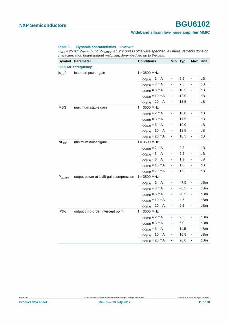
2. Pinning information
2.1 Pinning
2.2 Pin description
3. Ordering information
PL(1dB) output power at 1 dB gain compression
f = 450 MHz - 5.0 - dBm
f = 900 MHz - 5.5 - dBm
f = 2400 MHz; ICC(tot) = 6 mA - 0 - dBm
IP3O output third-order intercept point
f = 450 MHz - 5.5 - dBm
f = 900 MHz - 6.0 - dBm
f = 2400 MHz; ICC(tot) = 6 mA - 11.5 - dBm
Table 1. Quick reference data …continuedTamb = 25 C; VCC = 3.0 V; ICC(tot) = 3.0 mA; VENABLE 1.2 V unless otherwise specified. All measurements done on characterization board without matching, de-embedded up to the pins.
Symbol Parameter Conditions Min Typ Max Unit
Fig 1. Pin configuration
1
2
3
6
5
4
Transparent top view
Table 2. Pin description
Symbol Pin Description
VCC 1 supply voltage
n.c. 2 not connected
RF_IN 3 RF in
RF_OUT 4 RF out
ENABLE 5 enable
CUR_ADJ 6 current adjust
GND GND ground pad; RF and DC ground
Table 3. Ordering information
Type number Package
Name Description Version
BGU6102 HXSON6 plastic thermal enhanced super thin small outline package; no leads; 6 terminals; body 2 x 1.3 x 0.35 mm
SOT1209
OM7809 - 50 LNA evaluation board -
OM7810 - high-ohmic LNA evaluation board -
BGU6102 All information provided in this document is subject to legal disclaimers. © NXP B.V. 2012. All rights reserved.
Product data sheet Rev. 3 — 13 July 2012 2 of 20

NXP Semiconductors BGU6102Wideband silicon low-noise amplifier MMIC
4. Marking
5. Limiting values
[1] Due to internal ESD diode protection, the applied voltage should not exceed the specified maximum in order to avoid excess current.
[2] The RF input is directly coupled to the base of the RF transistor.
6. Thermal characteristics
7. Static characteristics
[1] ICC(tot) = ICC + IRF_OUT + IR_BIAS.
[2] Configurable with external resistor.
Table 4. Marking
Type number Marking Description
BGU6102 1B* * = p : made in Hong Kong
* = t : made in Malaysia
* = W : made in China
Table 5. Limiting valuesIn accordance with the Absolute Maximum Rating System (IEC 60134).
Symbol Parameter Conditions Min Max Unit
VCC supply voltage RF input, AC coupled - 5.5 V
VENABLE voltage on pin ENABLE [1] 0.5 VCC + 1.8 V
VRF_IN voltage on pin IN DC [2] 0.5 +0.9 V
VRF_OUT voltage on pin RF_OUT DC 0.5 VCC + 1.8 V
ICC(tot) total supply current VCC = 5.0 V - 40 mA
Tstg storage temperature 55 +150 C
Tj junction temperature - 150 C
VESD electrostatic discharge voltage Human Body Model (HBM); according to JEDEC standard 22-A114E
- 3000 V
Charged Device Model (CDM); according to JEDEC standard 22-C101B
- 500 V
Table 6. Thermal characteristics
Symbol Parameter Conditions Typ Unit
Rth(j-sp) thermal resistance from junction to solder point 110 K/W
Table 7. Static characteristics
Symbol Parameter Conditions Min Typ Max Unit
VCC supply voltage RF input, AC coupled 1.5 - 5.0 V
ICC(tot) total supply current VCC = 3.0 V [1][2] 2.1 - 21 mA
VENABLE 0.4 V [1] - - 0.01 mA
Tamb ambient temperature 40 +25 +85 C
BGU6102 All information provided in this document is subject to legal disclaimers. © NXP B.V. 2012. All rights reserved.
Product data sheet Rev. 3 — 13 July 2012 3 of 20

NXP Semiconductors BGU6102Wideband silicon low-noise amplifier MMIC
8. Dynamic characteristics
Table 8. Dynamic characteristicsTamb = 25 C; VCC = 3.0 V; VENABLE 1.2 V unless otherwise specified. All measurements done on characterization board without matching, de-embedded up to the pins.
Symbol Parameter Conditions Min Typ Max Unit
100 MHz frequency
s212 insertion power gain f = 100 MHz
ICC(tot) = 2 mA - 16.0 - dB
ICC(tot) = 3 mA - 19.5 - dB
ICC(tot) = 6 mA - 24.5 - dB
ICC(tot) = 10 mA - 28.0 - dB
ICC(tot) = 20 mA - 31.5 - dB
MSG maximum stable gain f = 100 MHz
ICC(tot) = 2 mA - 29.0 - dB
ICC(tot) = 3 mA - 31.0 - dB
ICC(tot) = 6 mA - 33.5 - dB
ICC(tot) = 10 mA - 35.5 - dB
ICC(tot) = 20 mA - 37.5 - dB
NFmin minimum noise figure f = 100 MHz
ICC(tot) = 2 mA - 0.8 - dB
ICC(tot) = 3 mA - 0.7 - dB
ICC(tot) = 6 mA - 0.8 - dB
ICC(tot) = 10 mA - 0.8 - dB
ICC(tot) = 20 mA - 1.0 - dB
PL(1dB) output power at 1 dB gain compression f = 100 MHz
ICC(tot) = 2 mA - 6.0 - dBm
ICC(tot) = 3 mA - 4.5 - dBm
ICC(tot) = 6 mA - 0.5 - dBm
ICC(tot) = 10 mA - 4.0 - dBm
ICC(tot) = 20 mA - 9.5 - dBm
IP3O output third-order intercept point f = 100 MHz
ICC(tot) = 2 mA - 3.0 - dBm
ICC(tot) = 3 mA - 5.5 - dBm
ICC(tot) = 6 mA - 10.5 - dBm
ICC(tot) = 10 mA - 14.5 - dBm
ICC(tot) = 20 mA - 19.5 - dBm
BGU6102 All information provided in this document is subject to legal disclaimers. © NXP B.V. 2012. All rights reserved.
Product data sheet Rev. 3 — 13 July 2012 4 of 20

NXP Semiconductors BGU6102Wideband silicon low-noise amplifier MMIC
150 MHz frequency
s212 insertion power gain f = 150 MHz
ICC(tot) = 2 mA - 16.0 - dB
ICC(tot) = 3 mA - 19.0 - dB
ICC(tot) = 6 mA - 24.5 - dB
ICC(tot) = 10 mA - 27.5 - dB
ICC(tot) = 20 mA - 31.0 - dB
MSG maximum stable gain f = 150 MHz
ICC(tot) = 2 mA - 27.5 - dB
ICC(tot) = 3 mA - 29.0 - dB
ICC(tot) = 6 mA - 32.0 - dB
ICC(tot) = 10 mA - 34.0 - dB
ICC(tot) = 20 mA - 36.0 - dB
NFmin minimum noise figure f = 150 MHz
ICC(tot) = 2 mA - 0.8 - dB
ICC(tot) = 3 mA - 0.7 - dB
ICC(tot) = 6 mA - 0.8 - dB
ICC(tot) = 10 mA - 0.8 - dB
ICC(tot) = 20 mA - 1.0 - dB
PL(1dB) output power at 1 dB gain compression f = 150 MHz
ICC(tot) = 2 mA - 6.5 - dBm
ICC(tot) = 3 mA - 4.5 - dBm
ICC(tot) = 6 mA - 0.0 - dBm
ICC(tot) = 10 mA - 3.5 - dBm
ICC(tot) = 20 mA - 9.0 - dBm
IP3O output third-order intercept point f = 150 MHz
ICC(tot) = 2 mA - 3.0 - dBm
ICC(tot) = 3 mA - 5.5 - dBm
ICC(tot) = 6 mA - 10.5 - dBm
ICC(tot) = 10 mA - 14.5 - dBm
ICC(tot) = 20 mA - 19.5 - dBm
Table 8. Dynamic characteristics …continuedTamb = 25 C; VCC = 3.0 V; VENABLE 1.2 V unless otherwise specified. All measurements done on characterization board without matching, de-embedded up to the pins.
Symbol Parameter Conditions Min Typ Max Unit
BGU6102 All information provided in this document is subject to legal disclaimers. © NXP B.V. 2012. All rights reserved.
Product data sheet Rev. 3 — 13 July 2012 5 of 20

NXP Semiconductors BGU6102Wideband silicon low-noise amplifier MMIC
450 MHz frequency
s212 insertion power gain f = 450 MHz
ICC(tot) = 2 mA - 15.5 - dB
ICC(tot) = 3 mA - 18.5 - dB
ICC(tot) = 6 mA - 23.0 - dB
ICC(tot) = 10 mA - 26.0 - dB
ICC(tot) = 20 mA - 29.0 - dB
MSG maximum stable gain f = 450 MHz
ICC(tot) = 2 mA - 22.5 - dB
ICC(tot) = 3 mA - 24.5 - dB
ICC(tot) = 6 mA - 27.0 - dB
ICC(tot) = 10 mA - 29.0 - dB
ICC(tot) = 20 mA - 31.0 - dB
NFmin minimum noise figure f = 450 MHz
ICC(tot) = 2 mA - 0.8 - dB
ICC(tot) = 3 mA - 0.7 - dB
ICC(tot) = 6 mA - 0.8 - dB
ICC(tot) = 10 mA - 0.8 - dB
ICC(tot) = 20 mA - 1.0 - dB
PL(1dB) output power at 1 dB gain compression f = 450 MHz
ICC(tot) = 2 mA - 7.0 - dBm
ICC(tot) = 3 mA - 5.0 - dBm
ICC(tot) = 6 mA - 0.5 - dBm
ICC(tot) = 10 mA - 3.0 - dBm
ICC(tot) = 20 mA - 9.0 - dBm
IP3O output third-order intercept point f = 450 MHz
ICC(tot) = 2 mA - 3.0 - dBm
ICC(tot) = 3 mA - 5.5 - dBm
ICC(tot) = 6 mA - 10.5 - dBm
ICC(tot) = 10 mA - 14.5 - dBm
ICC(tot) = 20 mA - 19.5 - dBm
Table 8. Dynamic characteristics …continuedTamb = 25 C; VCC = 3.0 V; VENABLE 1.2 V unless otherwise specified. All measurements done on characterization board without matching, de-embedded up to the pins.
Symbol Parameter Conditions Min Typ Max Unit
BGU6102 All information provided in this document is subject to legal disclaimers. © NXP B.V. 2012. All rights reserved.
Product data sheet Rev. 3 — 13 July 2012 6 of 20

NXP Semiconductors BGU6102Wideband silicon low-noise amplifier MMIC
900 MHz frequency
s212 insertion power gain f = 900 MHz
ICC(tot) = 2 mA - 14.0 - dB
ICC(tot) = 3 mA - 16.5 - dB
ICC(tot) = 6 mA - 20.5 - dB
ICC(tot) = 10 mA - 23.0 - dB
ICC(tot) = 20 mA - 25.0 - dB
MSG maximum stable gain f = 900 MHz
ICC(tot) = 2 mA - 19.5 - dB
ICC(tot) = 3 mA - 21.5 - dB
ICC(tot) = 6 mA - 24.0 - dB
ICC(tot) = 10 mA - 26.0 - dB
ICC(tot) = 20 mA - 28.0 - dB
NFmin minimum noise figure f = 900 MHz
ICC(tot) = 2 mA - 0.8 - dB
ICC(tot) = 3 mA - 0.8 - dB
ICC(tot) = 6 mA - 0.7 - dB
ICC(tot) = 10 mA - 0.8 - dB
ICC(tot) = 20 mA - 1.0 - dB
PL(1dB) output power at 1 dB gain compression f = 900 MHz
ICC(tot) = 2 mA - 7.5 - dBm
ICC(tot) = 3 mA - 5.5 - dBm
ICC(tot) = 6 mA - 0.5 - dBm
ICC(tot) = 10 mA - 3.5 - dBm
ICC(tot) = 20 mA - 10.0 - dBm
IP3O output third-order intercept point f = 900 MHz
ICC(tot) = 2 mA - 3.5 - dBm
ICC(tot) = 3 mA - 6.0 - dBm
ICC(tot) = 6 mA - 11.5 - dBm
ICC(tot) = 10 mA - 15.0 - dBm
ICC(tot) = 20 mA - 21.0 - dBm
Table 8. Dynamic characteristics …continuedTamb = 25 C; VCC = 3.0 V; VENABLE 1.2 V unless otherwise specified. All measurements done on characterization board without matching, de-embedded up to the pins.
Symbol Parameter Conditions Min Typ Max Unit
BGU6102 All information provided in this document is subject to legal disclaimers. © NXP B.V. 2012. All rights reserved.
Product data sheet Rev. 3 — 13 July 2012 7 of 20

NXP Semiconductors BGU6102Wideband silicon low-noise amplifier MMIC
1500 MHz frequency
s212 insertion power gain f = 1500 MHz
ICC(tot) = 2 mA - 11.5 - dB
ICC(tot) = 3 mA - 14.0 - dB
ICC(tot) = 6 mA - 17.5 - dB
ICC(tot) = 10 mA - 19.5 - dB
ICC(tot) = 20 mA - 21.0 - dB
MSG maximum stable gain f = 1500 MHz
ICC(tot) = 2 mA - 18.0 - dB
ICC(tot) = 3 mA - 19.5 - dB
ICC(tot) = 6 mA - 22.0 - dB
ICC(tot) = 10 mA - 24.0 - dB
ICC(tot) = 20 mA - 25.5 - dB
NFmin minimum noise figure f = 1500 MHz
ICC(tot) = 2 mA - 1.0 - dB
ICC(tot) = 3 mA - 1.0 - dB
ICC(tot) = 6 mA - 0.9 - dB
ICC(tot) = 10 mA - 0.9 - dB
ICC(tot) = 20 mA - 1.0 - dB
PL(1dB) output power at 1 dB gain compression f = 1500 MHz
ICC(tot) = 2 mA - 7.5 - dBm
ICC(tot) = 3 mA - 5.5 - dBm
ICC(tot) = 6 mA - 0.0 - dBm
ICC(tot) = 10 mA - 4.0 - dBm
ICC(tot) = 20 mA - 10.5 - dBm
IP3O output third-order intercept point f = 1500 MHz
ICC(tot) = 2 mA - 3.5 - dBm
ICC(tot) = 3 mA - 6.5 - dBm
ICC(tot) = 6 mA - 12.5 - dBm
ICC(tot) = 10 mA - 16.5 - dBm
ICC(tot) = 20 mA - 21.5 - dBm
Table 8. Dynamic characteristics …continuedTamb = 25 C; VCC = 3.0 V; VENABLE 1.2 V unless otherwise specified. All measurements done on characterization board without matching, de-embedded up to the pins.
Symbol Parameter Conditions Min Typ Max Unit
BGU6102 All information provided in this document is subject to legal disclaimers. © NXP B.V. 2012. All rights reserved.
Product data sheet Rev. 3 — 13 July 2012 8 of 20

NXP Semiconductors BGU6102Wideband silicon low-noise amplifier MMIC
1900 MHz frequency
s212 insertion power gain f = 1900 MHz
ICC(tot) = 2 mA - 10.5 - dB
ICC(tot) = 3 mA - 12.5 - dB
ICC(tot) = 6 mA - 16.0 - dB
ICC(tot) = 10 mA - 17.5 - dB
ICC(tot) = 20 mA - 19.0 - dB
MSG maximum stable gain f = 1900 MHz
ICC(tot) = 2 mA - 17.0 - dB
ICC(tot) = 3 mA - 18.5 - dB
ICC(tot) = 6 mA - 21.5 - dB
ICC(tot) = 10 mA - 23.0 - dB
ICC(tot) = 20 mA - 24.5 - dB
NFmin minimum noise figure f = 1900 MHz
ICC(tot) = 2 mA - 1.1 - dB
ICC(tot) = 3 mA - 1.1 - dB
ICC(tot) = 6 mA - 1.0 - dB
ICC(tot) = 10 mA - 1.0 - dB
ICC(tot) = 20 mA - 1.1 - dB
PL(1dB) output power at 1 dB gain compression f = 1900 MHz
ICC(tot) = 2 mA - 7.5 - dBm
ICC(tot) = 3 mA - 5.5 - dBm
ICC(tot) = 6 mA - 0.0 - dBm
ICC(tot) = 10 mA - 4.5 - dBm
ICC(tot) = 20 mA - 10.5 - dBm
IP3O output third-order intercept point f = 1900 MHz
ICC(tot) = 2 mA - 3.0 - dBm
ICC(tot) = 3 mA - 6.5 - dBm
ICC(tot) = 6 mA - 12.0 - dBm
ICC(tot) = 10 mA - 16.0 - dBm
ICC(tot) = 20 mA - 21 - dBm
Table 8. Dynamic characteristics …continuedTamb = 25 C; VCC = 3.0 V; VENABLE 1.2 V unless otherwise specified. All measurements done on characterization board without matching, de-embedded up to the pins.
Symbol Parameter Conditions Min Typ Max Unit
BGU6102 All information provided in this document is subject to legal disclaimers. © NXP B.V. 2012. All rights reserved.
Product data sheet Rev. 3 — 13 July 2012 9 of 20

NXP Semiconductors BGU6102Wideband silicon low-noise amplifier MMIC
2400 MHz frequency
s212 insertion power gain f = 2400 MHz
ICC(tot) = 2 mA - 8.5 - dB
ICC(tot) = 3 mA - 11.0 - dB
ICC(tot) = 6 mA - 14.0 - dB
ICC(tot) = 10 mA - 15.5 - dB
ICC(tot) = 20 mA - 17.0 - dB
MSG maximum stable gain f = 2400 MHz
ICC(tot) = 2 mA - 16.5 - dB
ICC(tot) = 3 mA - 18.0 - dB
ICC(tot) = 6 mA - 20.5 - dB
ICC(tot) = 10 mA - 22.0 - dB
ICC(tot) = 20 mA - 23.0 - dB
NFmin minimum noise figure f = 2400 MHz
ICC(tot) = 2 mA - 1.5 - dB
ICC(tot) = 3 mA - 1.3 - dB
ICC(tot) = 6 mA - 1.2 - dB
ICC(tot) = 10 mA - 1.2 - dB
ICC(tot) = 20 mA - 1.3 - dB
PL(1dB) output power at 1 dB gain compression f = 2400 MHz
ICC(tot) = 2 mA - 7.5 - dBm
ICC(tot) = 3 mA - 5.0 - dBm
ICC(tot) = 6 mA - 0.0 - dBm
ICC(tot) = 10 mA - 4.5 - dBm
ICC(tot) = 20 mA - 10.5 - dBm
IP3O output third-order intercept point f = 2400 MHz
ICC(tot) = 2 mA - 2.5 - dBm
ICC(tot) = 3 mA - 6.0 - dBm
ICC(tot) = 6 mA - 11.5 - dBm
ICC(tot) = 10 mA - 16.0 - dBm
ICC(tot) = 20 mA - 20.0 - dBm
Table 8. Dynamic characteristics …continuedTamb = 25 C; VCC = 3.0 V; VENABLE 1.2 V unless otherwise specified. All measurements done on characterization board without matching, de-embedded up to the pins.
Symbol Parameter Conditions Min Typ Max Unit
BGU6102 All information provided in this document is subject to legal disclaimers. © NXP B.V. 2012. All rights reserved.
Product data sheet Rev. 3 — 13 July 2012 10 of 20
NXP Semiconductors BGU6102Wideband silicon low-noise amplifier MMIC
3500 MHz frequency
s212 insertion power gain f = 3500 MHz
ICC(tot) = 2 mA - 5.5 - dB
ICC(tot) = 3 mA - 7.5 - dB
ICC(tot) = 6 mA - 10.5 - dB
ICC(tot) = 10 mA - 12.0 - dB
ICC(tot) = 20 mA - 13.5 - dB
MSG maximum stable gain f = 3500 MHz
ICC(tot) = 2 mA - 16.0 - dB
ICC(tot) = 3 mA - 17.5 - dB
ICC(tot) = 6 mA - 19.0 - dB
ICC(tot) = 10 mA - 18.5 - dB
ICC(tot) = 20 mA - 18.5 - dB
NFmin minimum noise figure f = 3500 MHz
ICC(tot) = 2 mA - 2.3 - dB
ICC(tot) = 3 mA - 2.2 - dB
ICC(tot) = 6 mA - 1.9 - dB
ICC(tot) = 10 mA - 1.8 - dB
ICC(tot) = 20 mA - 1.9 - dB
PL(1dB) output power at 1 dB gain compression f = 3500 MHz
ICC(tot) = 2 mA - 7.5 - dBm
ICC(tot) = 3 mA - 5.5 - dBm
ICC(tot) = 6 mA - 0.5 - dBm
ICC(tot) = 10 mA - 4.5 - dBm
ICC(tot) = 20 mA - 9.5 - dBm
IP3O output third-order intercept point f = 3500 MHz
ICC(tot) = 2 mA - 2.5 - dBm
ICC(tot) = 3 mA - 6.0 - dBm
ICC(tot) = 6 mA - 11.5 - dBm
ICC(tot) = 10 mA - 16.5 - dBm
ICC(tot) = 20 mA - 20.0 - dBm
Table 8. Dynamic characteristics …continuedTamb = 25 C; VCC = 3.0 V; VENABLE 1.2 V unless otherwise specified. All measurements done on characterization board without matching, de-embedded up to the pins.
Symbol Parameter Conditions Min Typ Max Unit
BGU6102 All information provided in this document is subject to legal disclaimers. © NXP B.V. 2012. All rights reserved.
Product data sheet Rev. 3 — 13 July 2012 11 of 20

NXP Semiconductors BGU6102Wideband silicon low-noise amplifier MMIC
9. Enable control
Table 9. ENABLE (pin 5)40 C Tamb +85 C.
VENABLE (V) State
0.4 OFF
1.2 ON
Tamb = 25 C.
(1) VCC = 1.5 V
(2) VCC = 3 V
(3) VCC = 5 V
Tamb = 25 C.
(1) Rbias = OPEN
(2) Rbias = 12 k
(3) Rbias = 4.7 k
(4) Rbias = 2.4 k
Fig 2. Supply current as a function of bias resistor; typical values
Fig 3. Supply current as a function of supply voltage and control voltage; typical values
aaa-001682
10
20
30
Icc(mA)
0
Rbias (Ω)10 105104102 103
(3)(3)(2)(2)
(1)
VCC, Vctrl (V)1 653 42
aaa-001683
10
20
30
ICC(mA)
0
(4)(4)
(3)(3)
(2)(2)
(1)
BGU6102 All information provided in this document is subject to legal disclaimers. © NXP B.V. 2012. All rights reserved.
Product data sheet Rev. 3 — 13 July 2012 12 of 20

NXP Semiconductors BGU6102Wideband silicon low-noise amplifier MMIC
Tamb = 25 C; VCC = 3 V; Pi = 30 dBm.
(1) f = 150 MHz
(2) f = 450 MHz
(3) f = 900 MHz
(4) f = 1500 MHz
(5) f = 1900 MHz
(6) f = 2400 MHz
(7) f = 3500 MHz
Tamb = 25 C; f1 = 900 MHz; f2 = 900.2 MHz; Pi = 30 dBm.
(1) VCC = 1.5 V
(2) VCC = 3 V
(3) VCC = 5 V
Fig 4. Insertion power gain (s212) as a function of total supply current; typical values
Fig 5. Output third-order intercept point as a function of total supply current; typical values
aaa-001684
Icc(tot) (mA)0 24168
20
10
30
40
lS21l2(dB)
0
(3)(3)
(7)(7)
(2)(2)
(1)
(6)(6)(5)(5)(4)(4)
ICC (tot) (mA)0 403010 20
aaa-001685
10
15
5
0
-5
20
25IP3O(dBm)
-10
(3)
(2)
(1)
BGU6102 All information provided in this document is subject to legal disclaimers. © NXP B.V. 2012. All rights reserved.
Product data sheet Rev. 3 — 13 July 2012 13 of 20

NXP Semiconductors BGU6102Wideband silicon low-noise amplifier MMIC
Tamb = 25 C; f = 900 MHz.
(1) VCC = 1.5 V
(2) VCC = 3 V
(3) VCC = 5 V
Tamb = 25 C; ICC(tot) = 3 mA; VCC = 3 V; Pi = 30 dBm.
Fig 6. Output power at 1 dB gain compression as a function of total supply current; typical values
Fig 7. Insertion power gain (s212) as a function of frequency; typical values
ICC(tot) (mA)0 403010 20
aaa-001686
PL(1dB)(dBm)
-15
-10
-5
0
5
10
15
20
(3)(3)
(2)(2)
(1)
f (MHz)0 400030001000 2000
aaa-001687
10
15
5
20
25
0
lS21l2(dB)
Tamb = 25 C; ICC(tot) = 3 mA; VCC = 3 V.
Fig 8. Minimum noise figure as a function of frequency; typical values
aaa-001688
1
2
3
NFmin(dB)
0
f (MHz)0 400030001000 2000
BGU6102 All information provided in this document is subject to legal disclaimers. © NXP B.V. 2012. All rights reserved.
Product data sheet Rev. 3 — 13 July 2012 14 of 20

NXP Semiconductors BGU6102Wideband silicon low-noise amplifier MMIC
10. Application information
Other applications available. Please contact your local sales representative for more information. Application note(s) available on the NXP web site.
All measurements are done with the SAM connector as reference plane.
10.1 High-ohmic FM radio characteristics
[1] See application note AN11091 for details.
10.2 50 ohm FM radio characteristics
[1] See application note AN11090 for details.
Table 10. AC characteristics[1]
Tamb = 25 C; VCC = 3.0 V; ICC(tot) = 3.1 mA; f = 100 MHz; measurements done on high-ohmic FM radio application board.
Symbol Parameter Conditions Min Typ Max Unit
s212 insertion power gain - 13 - dB
RLin input return loss - 1 - dB
RLout output return loss - 20 - dB
NF noise figure ZS = 50 - 1.0 - dB
Pi(1dB) input power at 1 dB gain compression - 23 - dBm
IP3I input third-order intercept point - 15 - dBm
Table 11. AC characteristics[1]
Tamb = 25 C; VCC = 2.8 V; ICC(tot) = 4.3 mA; f = 100 MHz; measurements done on 50 application board.
Symbol Parameter Conditions Min Typ Max Unit
s212 insertion power gain - 15 - dB
RLin input return loss - 10 - dB
RLout output return loss - 14 - dB
NF noise figure ZS = 50 - 1.3 1.8 dB
Pi(1dB) input power at 1 dB gain compression - 20 - dBm
IP3I input third-order intercept point - 12 - dBm
BGU6102 All information provided in this document is subject to legal disclaimers. © NXP B.V. 2012. All rights reserved.
Product data sheet Rev. 3 — 13 July 2012 15 of 20

NXP Semiconductors BGU6102Wideband silicon low-noise amplifier MMIC
11. Package outline
Fig 9. Package outline SOT1209
ReferencesOutlineversion
Europeanprojection Issue date
IEC JEDEC JEITA
SOT1209
sot1209_po
11-06-1011-09-15
Unit
mmmaxnommin
1.9 1.00.5 1.7
A
Dimensions
Note1. Dimension A is including plating thickness.
HXSON6: plastic thermal enhanced super thin small outline package; no leads;6 terminals; body 2 x 1.3 x 0.35 mm SOT1209
A1 b
0.151.0
D D1 E2 e e1
0.15
0.35 0.04 2.1 1.20.25 0.25
scale
L
0 1.5 mm
detail X
e1
e
e
shapeoptional (6×)
shapeoptional (4×)X
D1
E2 E1
A
A1
D
E
bL
5
4
6
2
3
1
terminal 1index area
terminal 1index area
1.2
1.4
E E1
1.2
1.4
BGU6102 All information provided in this document is subject to legal disclaimers. © NXP B.V. 2012. All rights reserved.
Product data sheet Rev. 3 — 13 July 2012 16 of 20

NXP Semiconductors BGU6102Wideband silicon low-noise amplifier MMIC
12. Abbreviations
13. Revision history
Table 12. Abbreviations
Acronym Description
AMR Automated Meter Reading
CMMB China Mobile Multimedia Broadcasting
ESD ElectroStatic Discharge
FM Frequency Modulation
ISM Industrial Scientific Medical
LNA Low-Noise Amplifier
MMIC Monolithic Microwave Integrated Circuit
RKE Remote Keyless Entry
TPMS Tire-Pressure Monitoring System
WLAN Wireless Local Area Network
Table 13. Revision history
Document ID Release date Data sheet status Change notice Supersedes
BGU6102 v.3 20120713 Product data sheet - BGU6102 v.2
Modifications: • Table 3 on page 2: swapped the descriptions of OM7809 and OM7810.
• Table 5 on page 3: changed the layout in order to remove the white gap on the next page and to reduce the page count with one page.
BGU6102 v.2 20120203 Product data sheet - BGU6102 v.1
BGU6102 v.1 20110921 Preliminary data sheet - -
BGU6102 All information provided in this document is subject to legal disclaimers. © NXP B.V. 2012. All rights reserved.
Product data sheet Rev. 3 — 13 July 2012 17 of 20

NXP Semiconductors BGU6102Wideband silicon low-noise amplifier MMIC
14. Legal information
14.1 Data sheet status
[1] Please consult the most recently issued document before initiating or completing a design.
[2] The term ‘short data sheet’ is explained in section “Definitions”.
[3] The product status of device(s) described in this document may have changed since this document was published and may differ in case of multiple devices. The latest product status information is available on the Internet at URL http://www.nxp.com.
14.2 Definitions
Draft — The document is a draft version only. The content is still under internal review and subject to formal approval, which may result in modifications or additions. NXP Semiconductors does not give any representations or warranties as to the accuracy or completeness of information included herein and shall have no liability for the consequences of use of such information.
Short data sheet — A short data sheet is an extract from a full data sheet with the same product type number(s) and title. A short data sheet is intended for quick reference only and should not be relied upon to contain detailed and full information. For detailed and full information see the relevant full data sheet, which is available on request via the local NXP Semiconductors sales office. In case of any inconsistency or conflict with the short data sheet, the full data sheet shall prevail.
Product specification — The information and data provided in a Product data sheet shall define the specification of the product as agreed between NXP Semiconductors and its customer, unless NXP Semiconductors and customer have explicitly agreed otherwise in writing. In no event however, shall an agreement be valid in which the NXP Semiconductors product is deemed to offer functions and qualities beyond those described in the Product data sheet.
14.3 Disclaimers
Limited warranty and liability — Information in this document is believed to be accurate and reliable. However, NXP Semiconductors does not give any representations or warranties, expressed or implied, as to the accuracy or completeness of such information and shall have no liability for the consequences of use of such information. NXP Semiconductors takes no responsibility for the content in this document if provided by an information source outside of NXP Semiconductors.
In no event shall NXP Semiconductors be liable for any indirect, incidental, punitive, special or consequential damages (including - without limitation - lost profits, lost savings, business interruption, costs related to the removal or replacement of any products or rework charges) whether or not such damages are based on tort (including negligence), warranty, breach of contract or any other legal theory.
Notwithstanding any damages that customer might incur for any reason whatsoever, NXP Semiconductors’ aggregate and cumulative liability towards customer for the products described herein shall be limited in accordance with the Terms and conditions of commercial sale of NXP Semiconductors.
Right to make changes — NXP Semiconductors reserves the right to make changes to information published in this document, including without limitation specifications and product descriptions, at any time and without notice. This document supersedes and replaces all information supplied prior to the publication hereof.
Suitability for use — NXP Semiconductors products are not designed, authorized or warranted to be suitable for use in life support, life-critical or safety-critical systems or equipment, nor in applications where failure or malfunction of an NXP Semiconductors product can reasonably be expected to result in personal injury, death or severe property or environmental damage. NXP Semiconductors and its suppliers accept no liability for inclusion and/or use of NXP Semiconductors products in such equipment or applications and therefore such inclusion and/or use is at the customer’s own risk.
Applications — Applications that are described herein for any of these products are for illustrative purposes only. NXP Semiconductors makes no representation or warranty that such applications will be suitable for the specified use without further testing or modification.
Customers are responsible for the design and operation of their applications and products using NXP Semiconductors products, and NXP Semiconductors accepts no liability for any assistance with applications or customer product design. It is customer’s sole responsibility to determine whether the NXP Semiconductors product is suitable and fit for the customer’s applications and products planned, as well as for the planned application and use of customer’s third party customer(s). Customers should provide appropriate design and operating safeguards to minimize the risks associated with their applications and products.
NXP Semiconductors does not accept any liability related to any default, damage, costs or problem which is based on any weakness or default in the customer’s applications or products, or the application or use by customer’s third party customer(s). Customer is responsible for doing all necessary testing for the customer’s applications and products using NXP Semiconductors products in order to avoid a default of the applications and the products or of the application or use by customer’s third party customer(s). NXP does not accept any liability in this respect.
Limiting values — Stress above one or more limiting values (as defined in the Absolute Maximum Ratings System of IEC 60134) will cause permanent damage to the device. Limiting values are stress ratings only and (proper) operation of the device at these or any other conditions above those given in the Recommended operating conditions section (if present) or the Characteristics sections of this document is not warranted. Constant or repeated exposure to limiting values will permanently and irreversibly affect the quality and reliability of the device.
Terms and conditions of commercial sale — NXP Semiconductors products are sold subject to the general terms and conditions of commercial sale, as published at http://www.nxp.com/profile/terms, unless otherwise agreed in a valid written individual agreement. In case an individual agreement is concluded only the terms and conditions of the respective agreement shall apply. NXP Semiconductors hereby expressly objects to applying the customer’s general terms and conditions with regard to the purchase of NXP Semiconductors products by customer.
No offer to sell or license — Nothing in this document may be interpreted or construed as an offer to sell products that is open for acceptance or the grant, conveyance or implication of any license under any copyrights, patents or other industrial or intellectual property rights.
Document status[1][2] Product status[3] Definition
Objective [short] data sheet Development This document contains data from the objective specification for product development.
Preliminary [short] data sheet Qualification This document contains data from the preliminary specification.
Product [short] data sheet Production This document contains the product specification.
BGU6102 All information provided in this document is subject to legal disclaimers. © NXP B.V. 2012. All rights reserved.
Product data sheet Rev. 3 — 13 July 2012 18 of 20

NXP Semiconductors BGU6102Wideband silicon low-noise amplifier MMIC
Export control — This document as well as the item(s) described herein may be subject to export control regulations. Export might require a prior authorization from competent authorities.
Non-automotive qualified products — Unless this data sheet expressly states that this specific NXP Semiconductors product is automotive qualified, the product is not suitable for automotive use. It is neither qualified nor tested in accordance with automotive testing or application requirements. NXP Semiconductors accepts no liability for inclusion and/or use of non-automotive qualified products in automotive equipment or applications.
In the event that customer uses the product for design-in and use in automotive applications to automotive specifications and standards, customer (a) shall use the product without NXP Semiconductors’ warranty of the product for such automotive applications, use and specifications, and (b) whenever customer uses the product for automotive applications beyond
NXP Semiconductors’ specifications such use shall be solely at customer’s own risk, and (c) customer fully indemnifies NXP Semiconductors for any liability, damages or failed product claims resulting from customer design and use of the product for automotive applications beyond NXP Semiconductors’ standard warranty and NXP Semiconductors’ product specifications.
Quick reference data — The Quick reference data is an extract of the product data given in the Limiting values and Characteristics sections of this document, and as such is not complete, exhaustive or legally binding.
14.4 TrademarksNotice: All referenced brands, product names, service names and trademarks are the property of their respective owners.
15. Contact information
For more information, please visit: http://www.nxp.com
For sales office addresses, please send an email to: [email protected]
BGU6102 All information provided in this document is subject to legal disclaimers. © NXP B.V. 2012. All rights reserved.
Product data sheet Rev. 3 — 13 July 2012 19 of 20

NXP Semiconductors BGU6102Wideband silicon low-noise amplifier MMIC
16. Contents
1 Product profile . . . . . . . . . . . . . . . . . . . . . . . . . . 11.1 General description . . . . . . . . . . . . . . . . . . . . . 11.2 Features and benefits . . . . . . . . . . . . . . . . . . . . 11.3 Applications . . . . . . . . . . . . . . . . . . . . . . . . . . . 11.4 Quick reference data . . . . . . . . . . . . . . . . . . . . 1
2 Pinning information. . . . . . . . . . . . . . . . . . . . . . 22.1 Pinning . . . . . . . . . . . . . . . . . . . . . . . . . . . . . . . 22.2 Pin description . . . . . . . . . . . . . . . . . . . . . . . . . 2
3 Ordering information. . . . . . . . . . . . . . . . . . . . . 2
4 Marking . . . . . . . . . . . . . . . . . . . . . . . . . . . . . . . . 3
5 Limiting values. . . . . . . . . . . . . . . . . . . . . . . . . . 3
6 Thermal characteristics . . . . . . . . . . . . . . . . . . 3
7 Static characteristics. . . . . . . . . . . . . . . . . . . . . 3
8 Dynamic characteristics . . . . . . . . . . . . . . . . . . 4
9 Enable control . . . . . . . . . . . . . . . . . . . . . . . . . 12
10 Application information. . . . . . . . . . . . . . . . . . 1510.1 High-ohmic FM radio characteristics . . . . . . . 1510.2 50 ohm FM radio characteristics. . . . . . . . . . . 15
11 Package outline . . . . . . . . . . . . . . . . . . . . . . . . 16
12 Abbreviations. . . . . . . . . . . . . . . . . . . . . . . . . . 17
13 Revision history. . . . . . . . . . . . . . . . . . . . . . . . 17
14 Legal information. . . . . . . . . . . . . . . . . . . . . . . 1814.1 Data sheet status . . . . . . . . . . . . . . . . . . . . . . 1814.2 Definitions. . . . . . . . . . . . . . . . . . . . . . . . . . . . 1814.3 Disclaimers . . . . . . . . . . . . . . . . . . . . . . . . . . . 1814.4 Trademarks. . . . . . . . . . . . . . . . . . . . . . . . . . . 19
15 Contact information. . . . . . . . . . . . . . . . . . . . . 19
16 Contents . . . . . . . . . . . . . . . . . . . . . . . . . . . . . . 20
© NXP B.V. 2012. All rights reserved.
For more information, please visit: http://www.nxp.comFor sales office addresses, please send an email to: [email protected]
Date of release: 13 July 2012
Document identifier: BGU6102
Please be aware that important notices concerning this document and the product(s)described herein, have been included in section ‘Legal information’.


![BGU6101 Wideband silicon low-noise amplifier MMIC · Wideband silicon low-noise amplifier MMIC 7. Static characteristics Table 7. Static characteristics [1] ICC(tot) = ICC + IRF_OUT](https://img.dokumen.tips/doc/110x75/5f8bbe3820a0400a6155b583/bgu6101-wideband-silicon-low-noise-amplifier-mmic-wideband-silicon-low-noise-amplifier.jpg)