Embed Size (px)
Citation preview
Bandgap references, sampling switchesBandgap references, sampling switchesTuesday, February 1st, 9:15 – 12:00
Snorre Aunet ([email protected])Nanoelectronics group
Department of InformaticsUniversity of Oslo
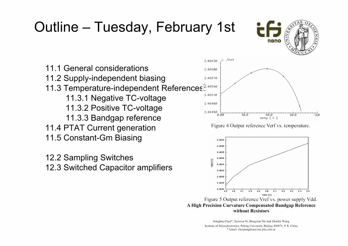
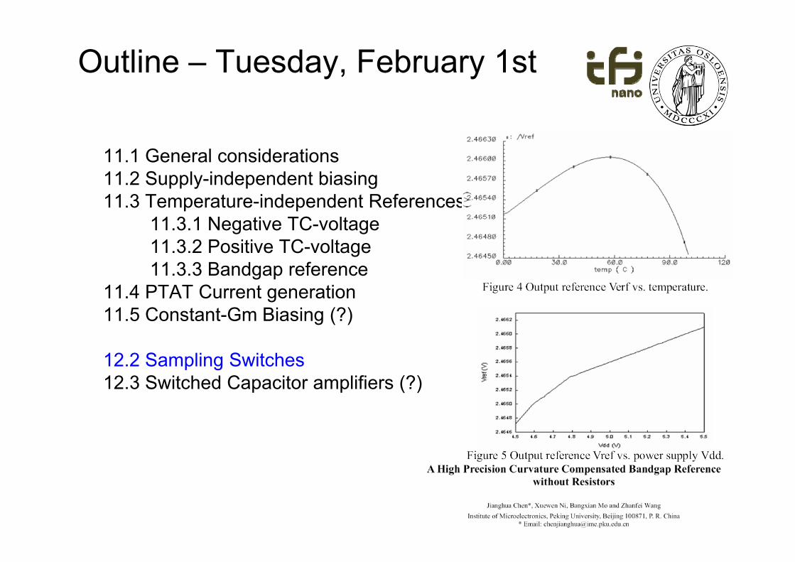
Outline – Tuesday, February 1st
11 1 General considerations11.1 General considerations11.2 Supply-independent biasing11.3 Temperature-independent References
11 3 1 N ti TC lt11.3.1 Negative TC-voltage11.3.2 Positive TC-voltage11.3.3 Bandgap reference
11.4 PTAT Current generation11.5 Constant-Gm Biasing
12.2 Sampling Switches12.3 Switched Capacitor amplifiers
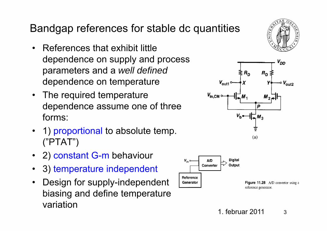
Bandgap references for stable dc quantities
• References that exhibit littledependence on supply and processp pp y pparameters and a well defineddependence on temperature
• The required temperaturedependence assume one of threeformsforms:
• 1) proportional to absolute temp. (”PTAT”)( PTAT )
• 2) constant G-m behaviour• 3) temperature independent• 3) temperature independent• Design for supply-independent
biasing and define temperaturebiasing and define temperaturevariation
31. februar 2011
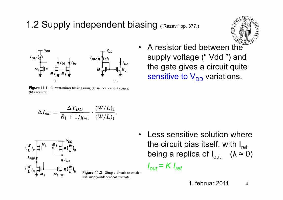
1.2 Supply independent biasing (”Razavi” pp. 377.)
• A resistor tied between thel lt (” Vdd ”) dsupply voltage (” Vdd ”) and
the gate gives a circuit quitesensitive to VDD variationssensitive to VDD variations.
• Less sensitive solution wherethe circuit bias itself with I fthe circuit bias itself, with Irefbeing a replica of Iout (λ ≈ 0)
• Iout = K IrefIout K Iref
41. februar 2011
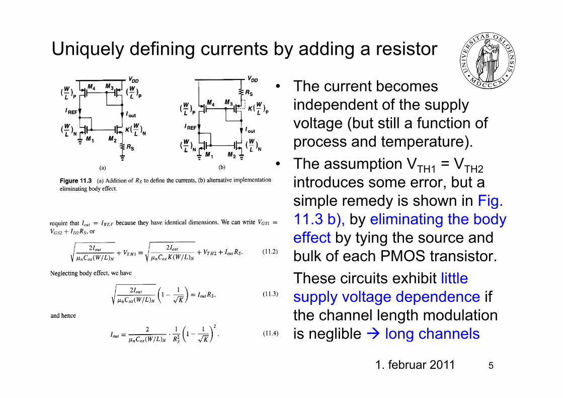
Uniquely defining currents by adding a resistor
• The current becomesindependent of the supplyindependent of the supplyvoltage (but still a function ofprocess and temperature).
• The assumption VTH1 = VTH2 introduces some error, but a simple remedy is shown in Figsimple remedy is shown in Fig. 11.3 b), by eliminating the body effect by tying the source and y y gbulk of each PMOS transistor.
• These circuits exhibit littlesupply voltage dependence ifthe channel length modulationis neglible long channelsis neglible long channels
51. februar 2011
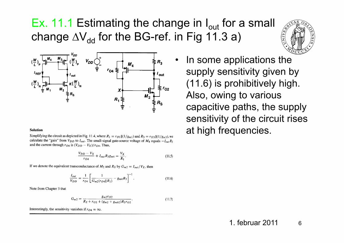
Ex. 11.1 Estimating the change in Iout for a smallchange ∆Vdd for the BG-ref in Fig 11 3 a)change ∆Vdd for the BG ref. in Fig 11.3 a)
• In some applications thesupply sensitivity given by (11.6) is prohibitively high. Also owing to variousAlso, owing to variouscapacitive paths, the supplysensitivity of the circuit risessensitivity of the circuit rises at high frequencies.
61. februar 2011
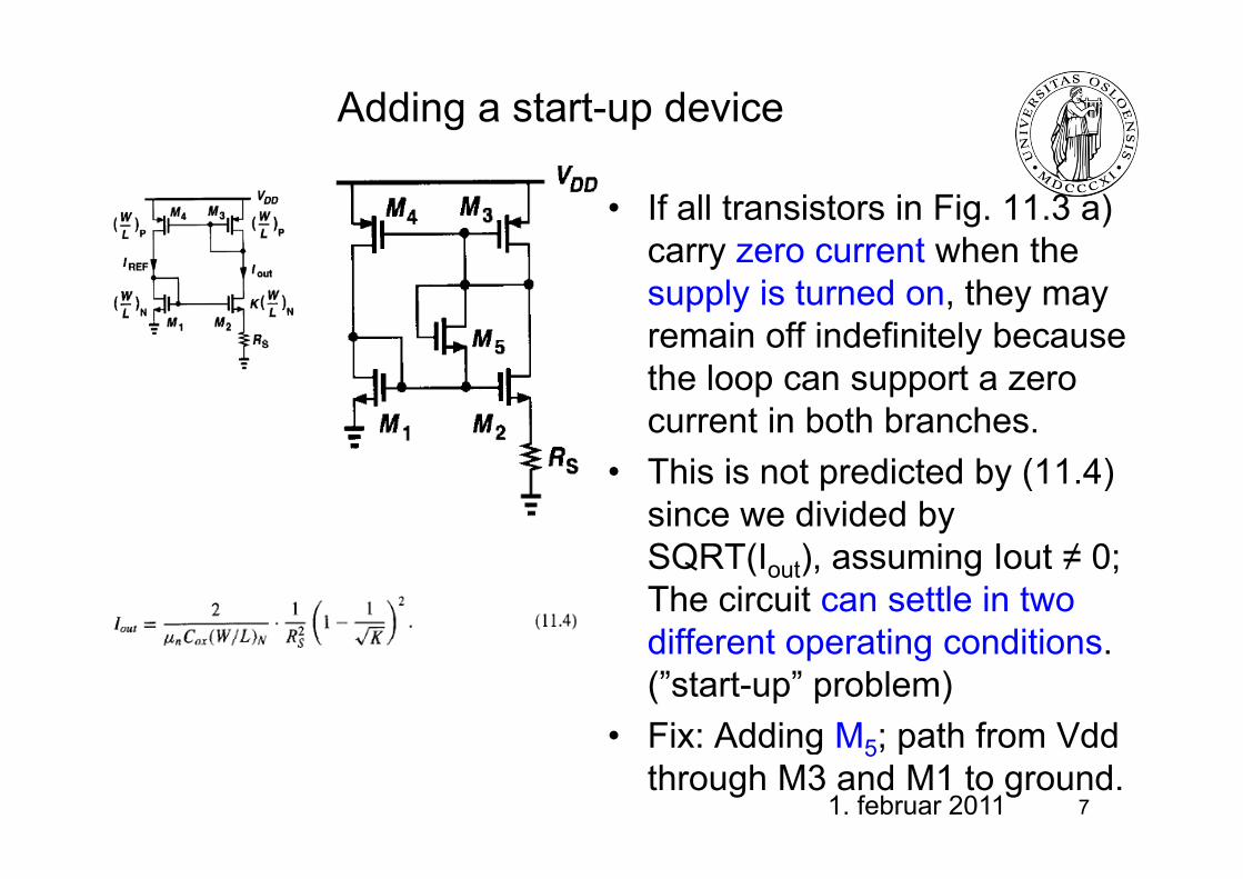
Adding a start-up device
• If all transistors in Fig. 11.3 a) t h thcarry zero current when the
supply is turned on, they mayremain off indefinitely becauseremain off indefinitely becausethe loop can support a zero current in both branches.
• This is not predicted by (11.4) since we divided by SQRT(Iout), assuming Iout ≠ 0; The circuit can settle in twodifferent operating conditionsdifferent operating conditions. (”start-up” problem)
• Fix: Adding M ; path from Vdd• Fix: Adding M5; path from Vddthrough M3 and M1 to ground.
71. februar 2011
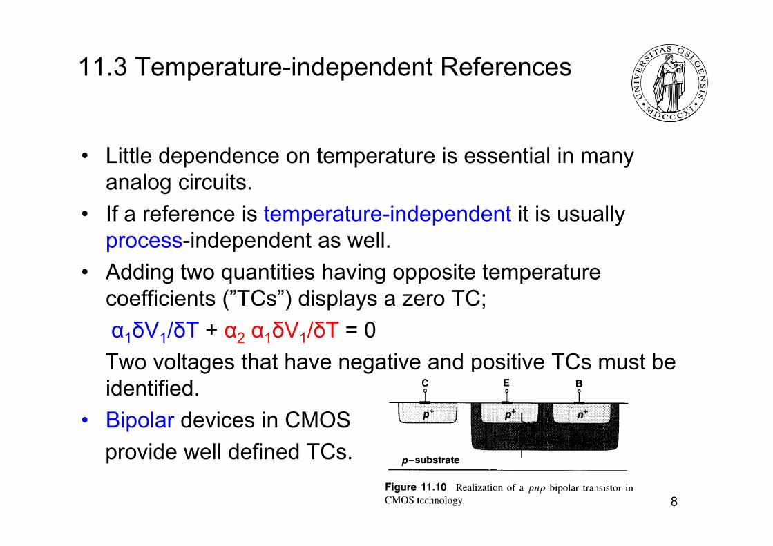
11.3 Temperature-independent References
Littl d d t t i ti l i• Little dependence on temperature is essential in manyanalog circuits.
• If a reference is temperature independent it is usually• If a reference is temperature-independent it is usuallyprocess-independent as well.
• Adding two quantities having opposite temperature• Adding two quantities having opposite temperaturecoefficients (”TCs”) displays a zero TC; α1δV1/δT + α2 α1δV1/δT = 0α1δV1/δT α2 α1δV1/δT 0Two voltages that have negative and positive TCs must be identified.
• Bipolar devices in CMOSprovide well defined TCs.provide well defined TCs.
81. februar 2011
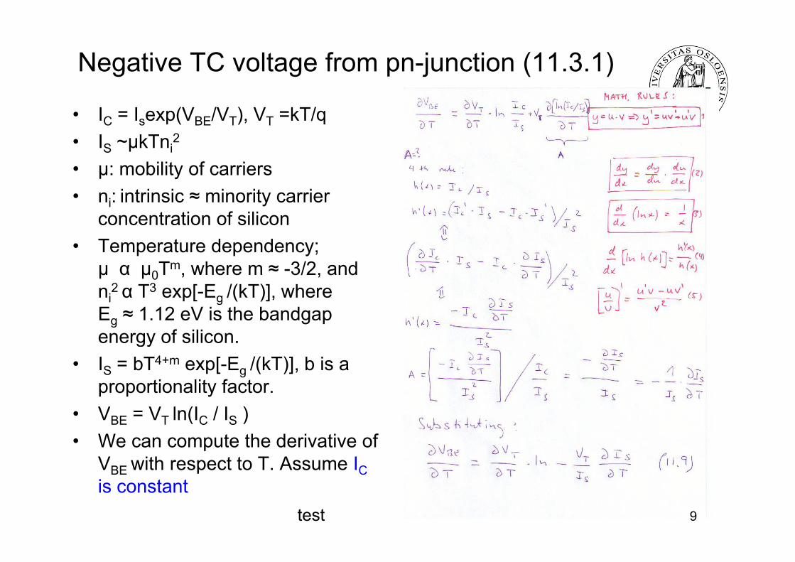
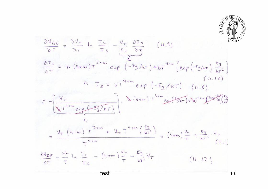
Negative TC voltage from pn-junction (11.3.1)
• IC = Isexp(VBE/VT), VT =kT/q• IS ~µkTni
2
• µ: mobility of carriers• ni: intrinsic ≈ minority carrier
concentration of siliconconcentration of silicon• Temperature dependency;
µ α µ0Tm, where m ≈ -3/2, and ni
2 α T3 exp[-Eg /(kT)], whereEg ≈ 1.12 eV is the bandgapenergy of silicon.gy
• IS = bT4+m exp[-Eg /(kT)], b is a proportionality factor.V V l (I / I )• VBE = VT ln(IC / IS )
• We can compute the derivative ofVBE with respect to T. Assume ICBE p Cis constant
test 9
test 10
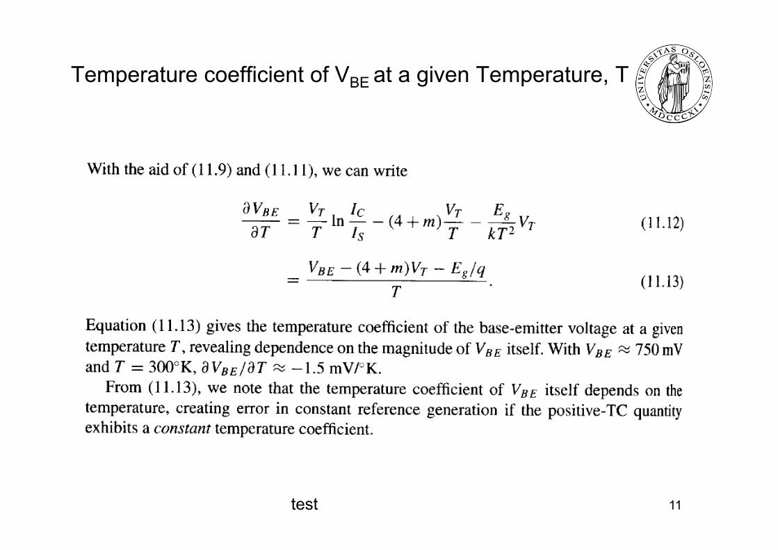
Temperature coefficient of VBE at a given Temperature, T
test 11
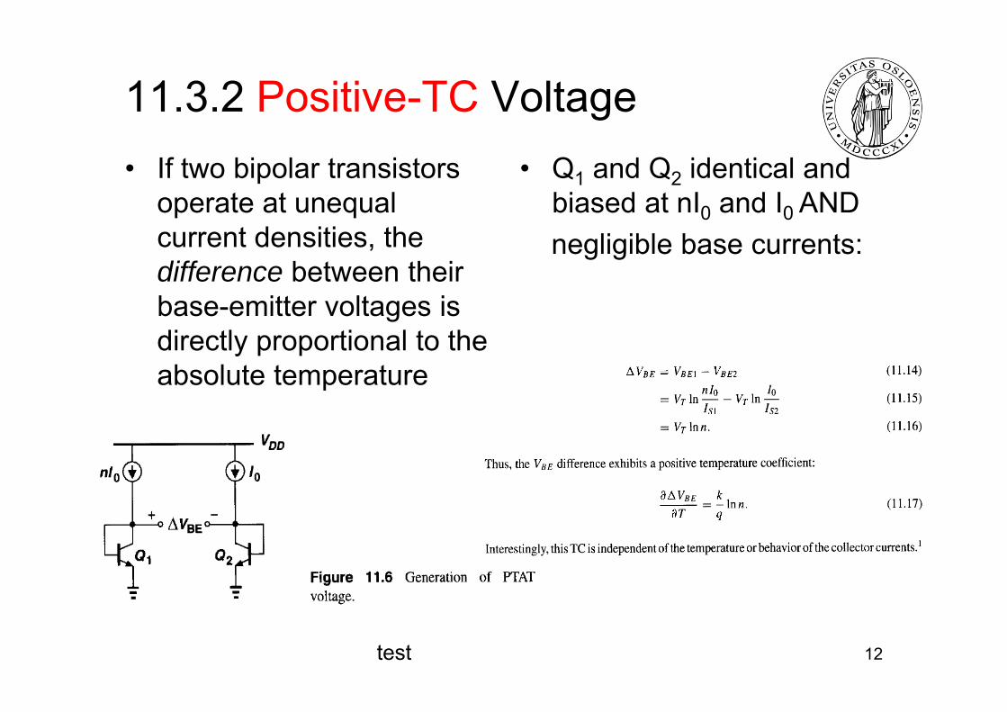
11.3.2 Positive-TC Voltageg• If two bipolar transistors
t t l• Q1 and Q2 identical and
bi d t I d I ANDoperate at unequalcurrent densities, thedifference between their
biased at nI0 and I0 ANDnegligible base currents:
difference between theirbase-emitter voltages is directly proportional to theyabsolute temperature
test 12
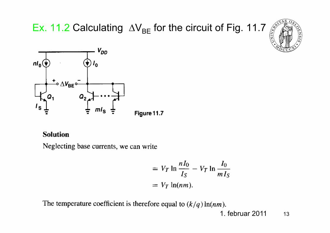
Ex. 11.2 Calculating ∆VBE for the circuit of Fig. 11.7
• In
131. februar 2011
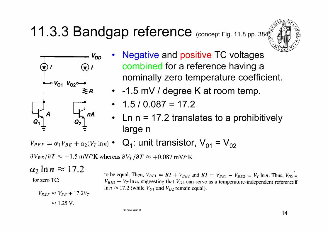
11.3.3 Bandgap reference (concept Fig. 11.8 pp. 384)g p ( p g pp )
• Negative and positive TC voltagesbi d f f h icombined for a reference having a
nominally zero temperature coefficient.• 1 5 mV / degree K at room temp• -1.5 mV / degree K at room temp.• 1.5 / 0.087 = 17.2
Ln n 17 2 translates to a prohibiti el• Ln n = 17.2 translates to a prohibitivelylarge n
• Q : unit transistor V = V• Q1: unit transistor, V01 = V02
Snorre Aunet14
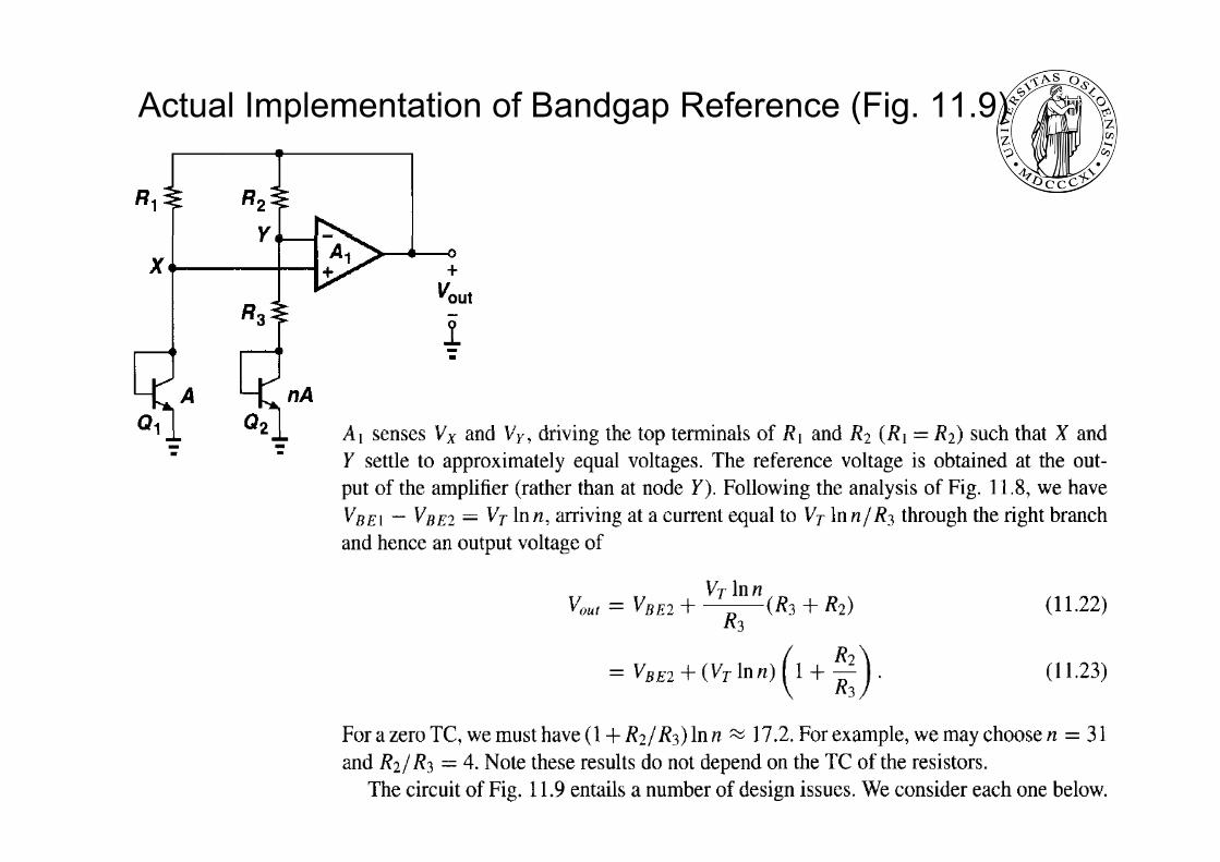
Actual Implementation of Bandgap Reference (Fig. 11.9)
151. februar 2011
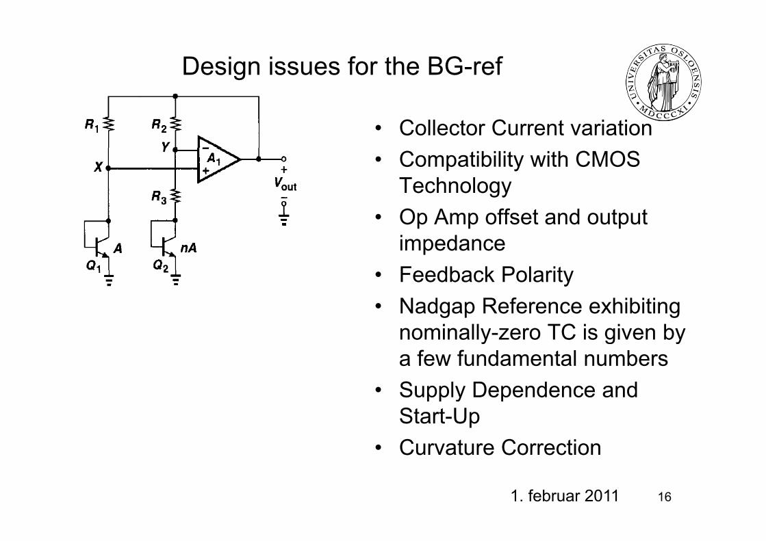
Design issues for the BG-ref
• Collector Current variation• Compatibility with CMOS
TechnologyO A ff t d t t• Op Amp offset and output impedanceFeedback Polarit• Feedback Polarity
• Nadgap Reference exhibitingnominally zero TC is given bynominally-zero TC is given by a few fundamental numbers
• Supply Dependence andSupply Dependence and Start-Up
• Curvature CorrectionCurvature Correction
161. februar 2011
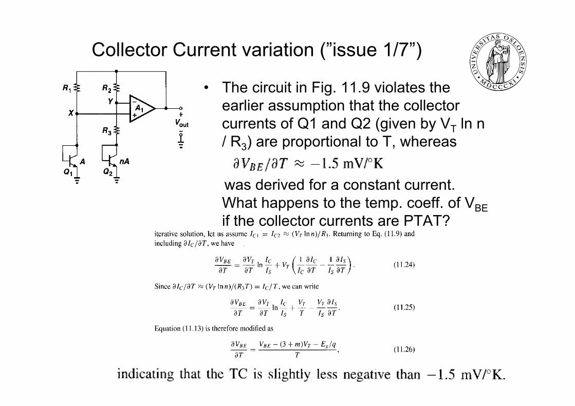
Collector Current variation (”issue 1/7”)
• The circuit in Fig. 11.9 violates theearlier assumption that the collectorpcurrents of Q1 and Q2 (given by VT ln n / R3) are proportional to T, whereas
was derived for a constant current. What happens to the temp coeff of VWhat happens to the temp. coeff. of VBE if the collector currents are PTAT?
171. februar 2011
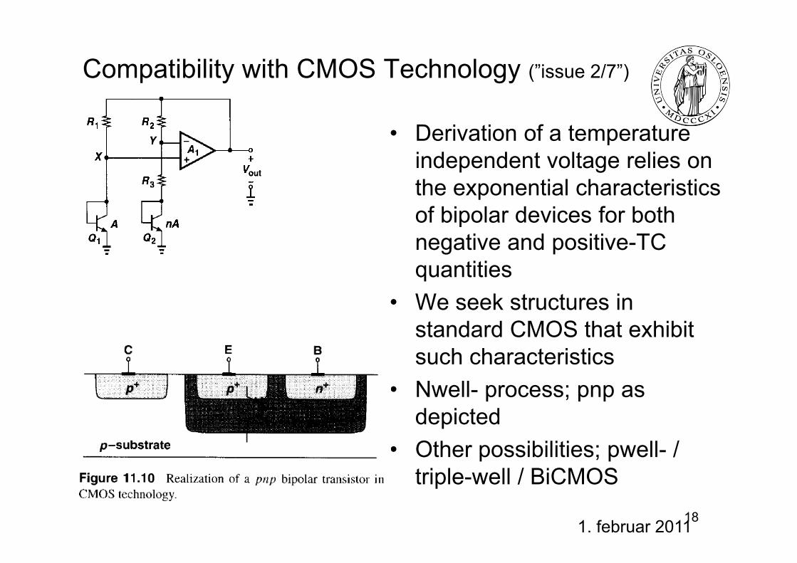
Compatibility with CMOS Technology (”issue 2/7”)
• Derivation of a temperaturei d d t lt liindependent voltage relies onthe exponential characteristicsof bipolar devices for bothof bipolar devices for bothnegative and positive-TCquantities
• We seek structures in standard CMOS that exhibitsuch characteristics
• Nwell- process; pnp as d i t ddepicted
• Other possibilities; pwell- / triple well / BiCMOStriple-well / BiCMOS
181. februar 2011
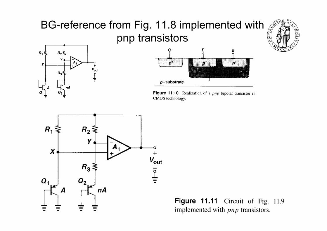
BG-reference from Fig. 11.8 implemented withpnp transistorspnp transistors
test 19
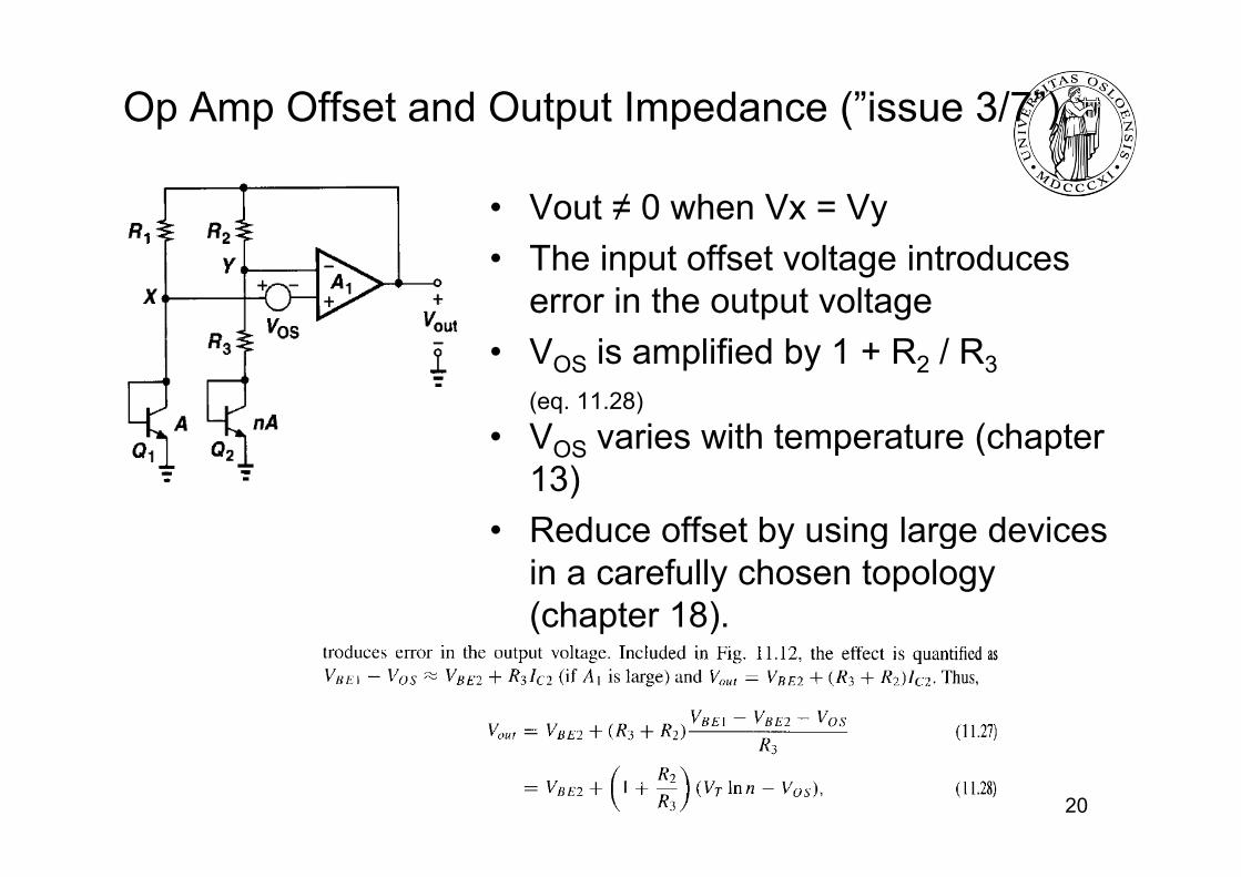
Op Amp Offset and Output Impedance (”issue 3/7”)
• Vout ≠ 0 when Vx = Vy• The input offset voltage introduces
error in the output voltageV i lifi d b 1 R / R• VOS is amplified by 1 + R2 / R3(eq. 11.28)
• V varies with temperature (chapter• VOS varies with temperature (chapter13)
• Reduce offset by using large devicesReduce offset by using large devicesin a carefully chosen topology(chapter 18).
201. februar 2011
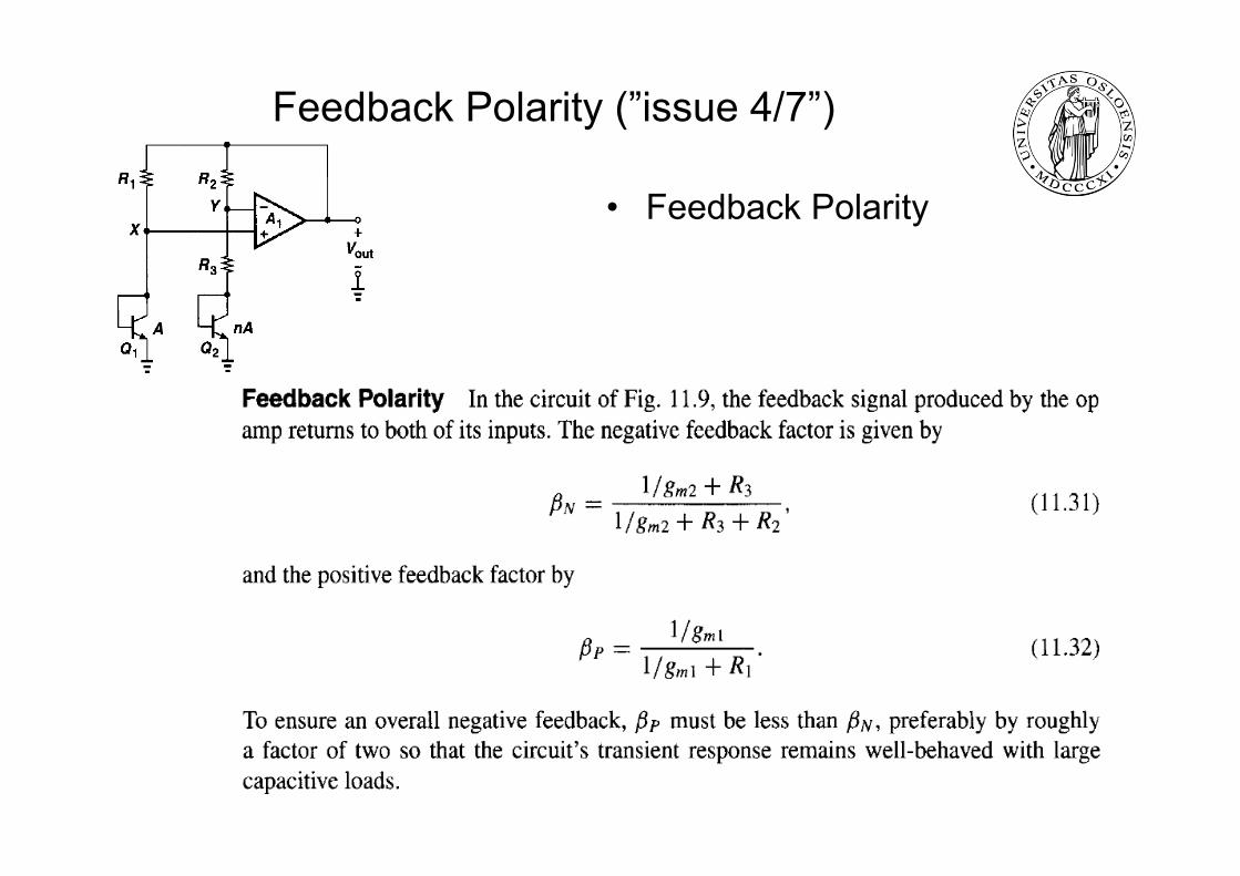
Feedback Polarity (”issue 4/7”)
• Feedback Polarity
211. februar 2011
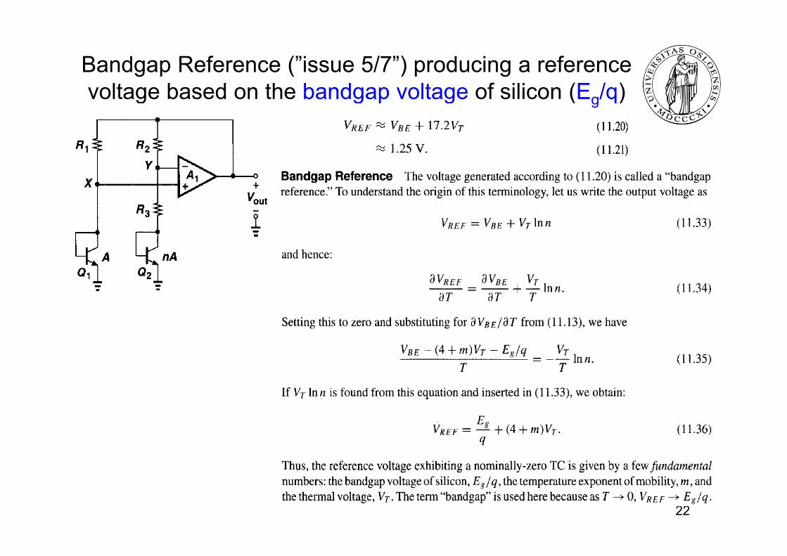
Bandgap Reference (”issue 5/7”) producing a referencevoltage based on the bandgap voltage of silicon (E /q)voltage based on the bandgap voltage of silicon (Eg/q)
22
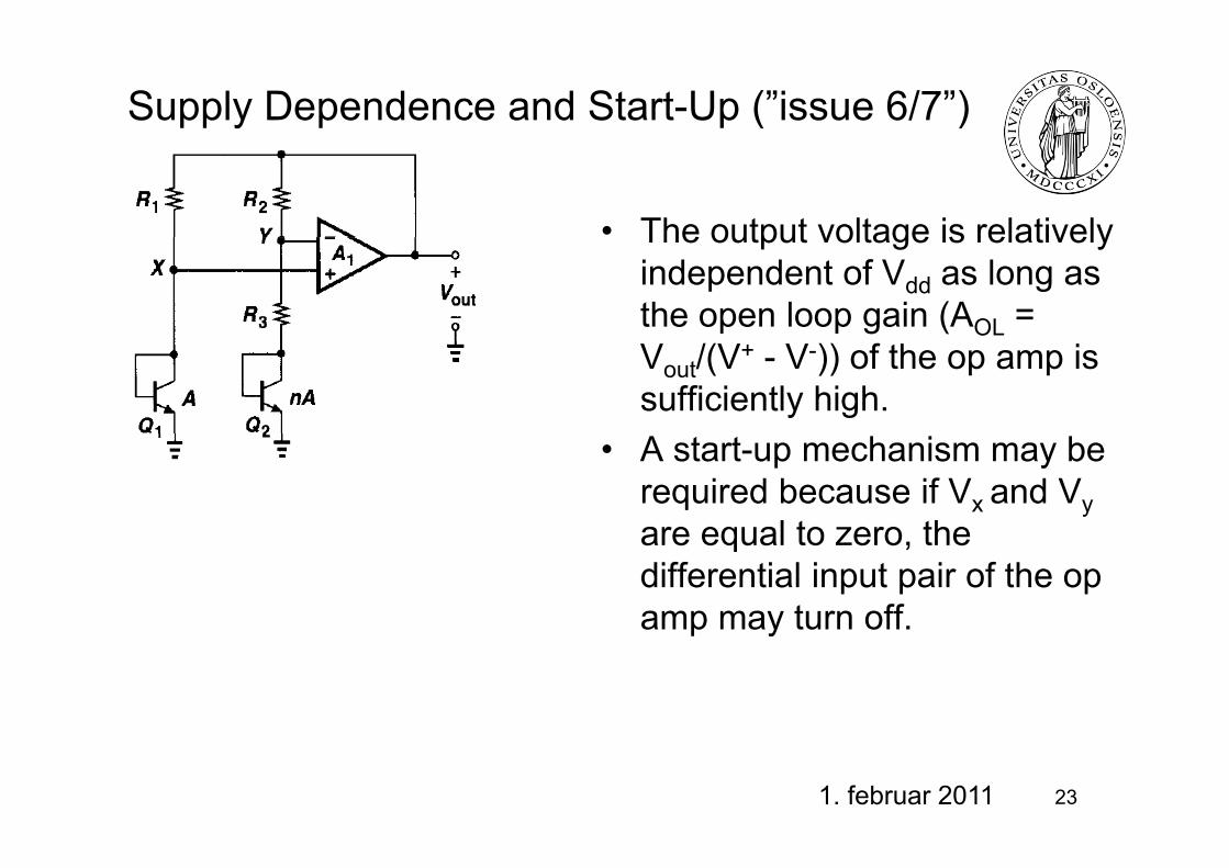
Supply Dependence and Start-Up (”issue 6/7”)
• The output voltage is relativelyThe output voltage is relativelyindependent of Vdd as long as the open loop gain (AOL = Vout/(V+ - V-)) of the op amp is sufficiently high.
• A start-up mechanism may be required because if Vx and Vyare equal to zero theare equal to zero, thedifferential input pair of the op amp may turn off.p y
231. februar 2011
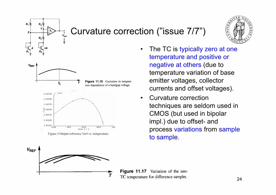
Curvature correction (”issue 7/7”)Curvature correction ( issue 7/7 )
• The TC is typically zero at onetemperature and positive or negative at others (due to temperature variation of base pemitter voltages, collectorcurrents and offset voltages).
• Curvature correction• Curvature correctiontechniques are seldom used in CMOS (but used in bipolar i l ) d t ff t dimpl.) due to offset- and process variations from sampleto sample.
24
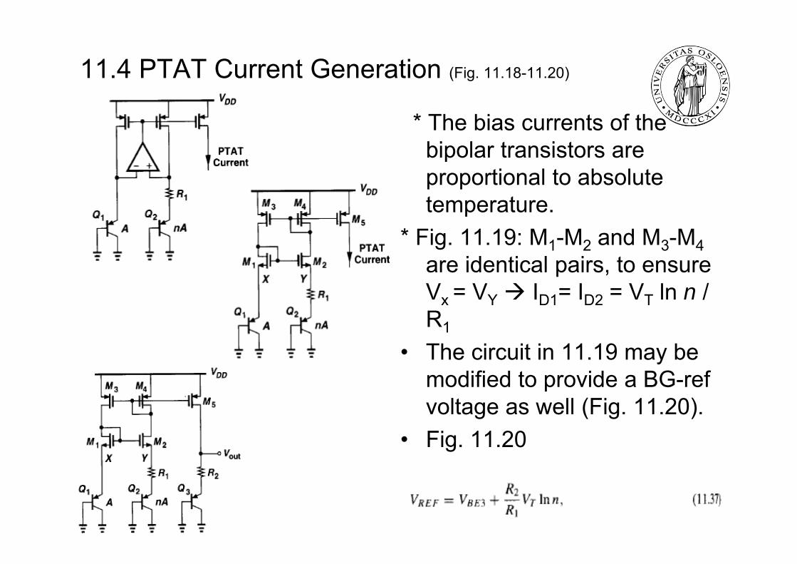
11.4 PTAT Current Generation (Fig. 11.18-11.20)
* The bias currents of thebipolar transistors arebipolar transistors areproportional to absolutetemperature.
* Fig. 11.19: M1-M2 and M3-M4are identical pairs, to ensureVx = VY ID1= ID2 = VT ln n / R1
Th i it i 11 19 b• The circuit in 11.19 may be modified to provide a BG-refvoltage as well (Fig 11 20)voltage as well (Fig. 11.20).
• Fig. 11.20
251. februar 2011
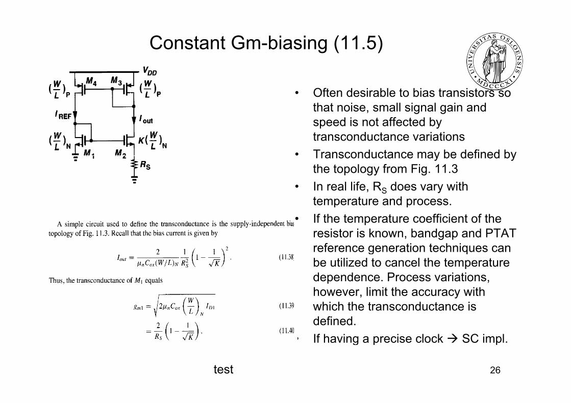
Constant Gm-biasing (11.5)
• Often desirable to bias transistors so that noise small signal gain andthat noise, small signal gain and speed is not affected by transconductance variations
• Transconductance may be defined byTransconductance may be defined by the topology from Fig. 11.3
• In real life, RS does vary withtemperature and processtemperature and process.
• If the temperature coefficient of theresistor is known, bandgap and PTAT reference generation techniques canreference generation techniques canbe utilized to cancel the temperaturedependence. Process variations, however limit the accuracy withhowever, limit the accuracy withwhich the transconductance is defined.
• If having a precise clock SC impl• If having a precise clock SC impl.
test 26
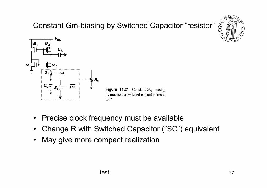
Constant Gm-biasing by Switched Capacitor ”resistor”
P i l k f t b il bl• Precise clock frequency must be available• Change R with Switched Capacitor (”SC”) equivalent• May give more compact realization
test 27
Outline – Tuesday, February 1st
11 1 General considerations11.1 General considerations11.2 Supply-independent biasing11.3 Temperature-independent References
11 3 1 N ti TC lt11.3.1 Negative TC-voltage11.3.2 Positive TC-voltage11.3.3 Bandgap reference
11.4 PTAT Current generation11.5 Constant-Gm Biasing (?)
12.2 Sampling Switches12.3 Switched Capacitor amplifiers (?)
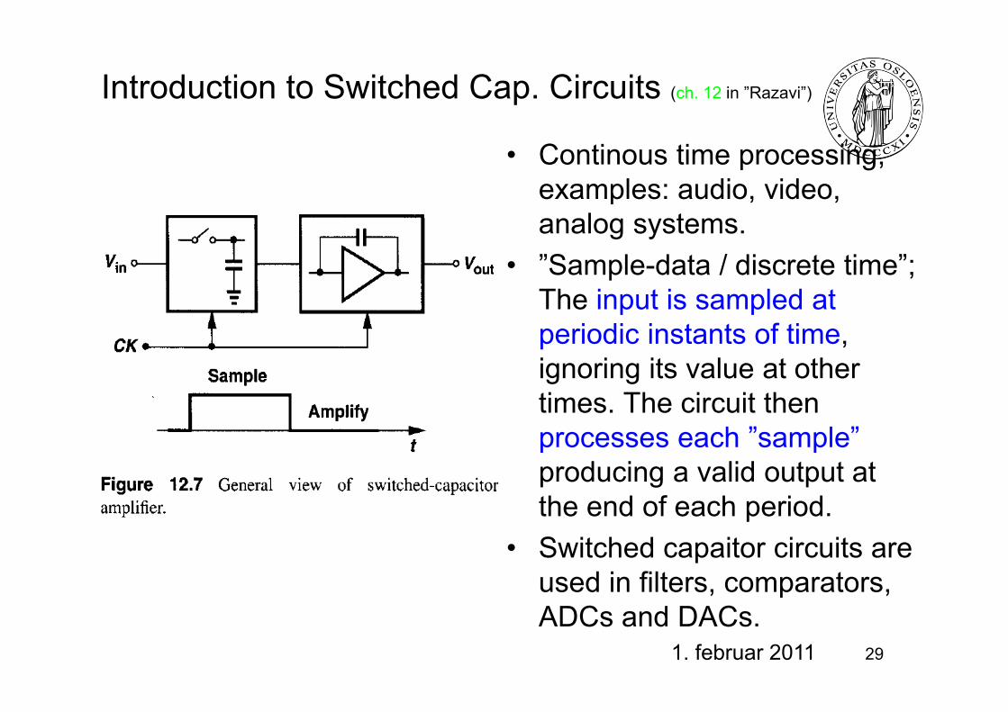
Introduction to Switched Cap. Circuits (ch. 12 in ”Razavi”)
• Continous time processing, examples: audio videoexamples: audio, video, analog systems.
• ”Sample-data / discrete time”; p ;The input is sampled at periodic instants of time, ignoring its value at othertimes. The circuit thenprocesses each ”sample”processes each sample producing a valid output at the end of each period.p
• Switched capaitor circuits areused in filters, comparators, ADCs and DACs.
291. februar 2011
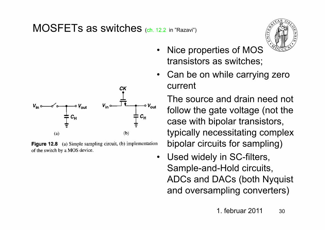
MOSFETs as switches (ch. 12.2 in ”Razavi”)
• Nice properties of MOS transistors as switches;transistors as switches;
• Can be on while carrying zero current
• The source and drain need not follow the gate voltage (not theg g (case with bipolar transistors, typically necessitating complexbi l i it f li )bipolar circuits for sampling)
• Used widely in SC-filters, Sample and Hold circuitsSample-and-Hold circuits, ADCs and DACs (both Nyquist and oversampling converters)and oversampling converters)
301. februar 2011
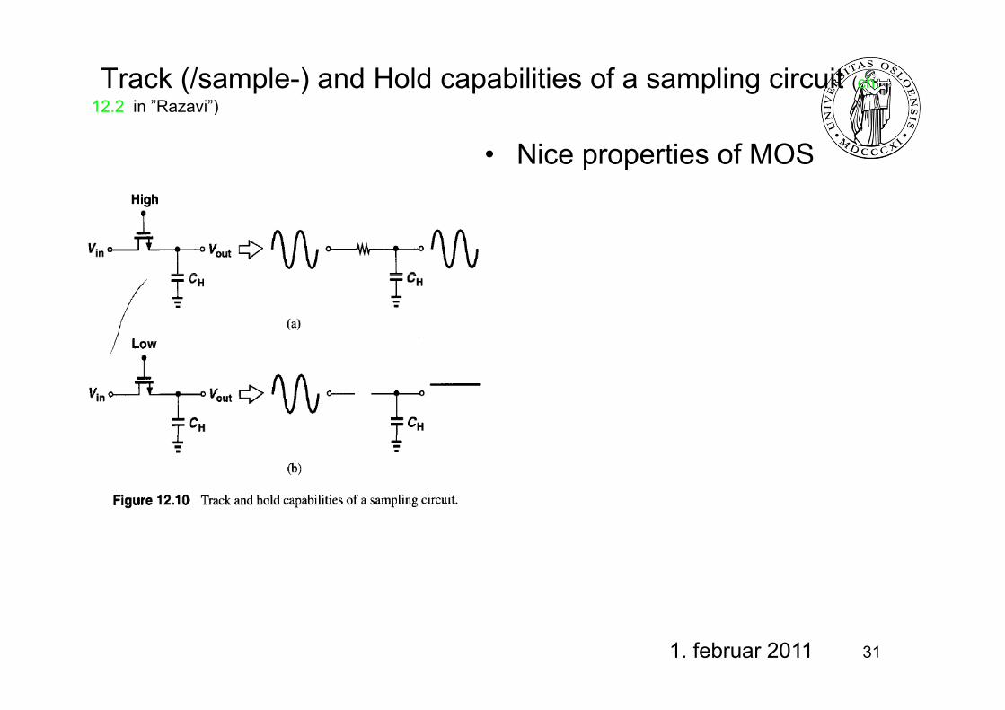
Track (/sample-) and Hold capabilities of a sampling circuit (ch. 12.2 in ”Razavi”))
• Nice properties of MOS
311. februar 2011
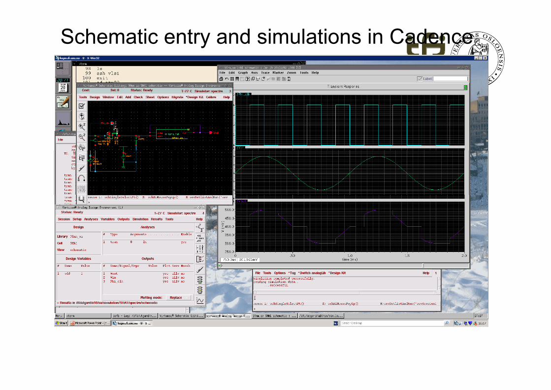
Schematic entry and simulations in Cadence
Next week:
• Sample and Hold circuits, Data converter fundamentals
• Messages are given on the INF4420 homepage.
• Questions: [email protected] , 22852703 / 90013264


![Voltage and Current References Bandgap References · Microsoft PowerPoint - IC_Slide6.ppt [Compatibility Mode] Author: dr shamsi Created Date: 12/25/2017 7:15:49 AM](https://img.dokumen.tips/doc/110x75/5f38973b3369d7587b64467f/voltage-and-current-references-bandgap-references-microsoft-powerpoint-icslide6ppt.jpg)


![[a.van Staveren]Structured Electronic Design - High-Performance Harmonic Oscillators and Bandgap References](https://img.dokumen.tips/doc/110x75/577d35ac1a28ab3a6b91163f/avan-staverenstructured-electronic-design-high-performance-harmonic-oscillators.jpg)