Embed Size (px)
Citation preview

D A T A S H E E T
B1505A Power Device Analyzer/Curve Tracer

Page 2Find us at www.keysight.com
Introduction
The Keysight Technologies, Inc. B1505A Power Device Analyzer/Curve Tracer is a single-box solution with next-generation curve tracer functionality that can accurately evaluate and characterize power devices at up to 10 kV and 1500 A. The B1505A is capable of handling all types of power device evaluation, with features that include a wide voltage and current range, fast pulsing capability (10 µs), µΩ level on-resistance measurement resolution and sub-pA level current measurement capability. In addition, an oscilloscope view permits visual verification of both current and voltage pulsed waveforms.
Two independent analog-to-digital (A/D) converters on each channel support a 2 µs sampling rate for accurate monitoring of the critical timings that can affect device behavior.
It can also perform fully automated capacitance measurements (such as Ciss, Coss and Crss) at high voltage biases (up to 3 kV). Moreover, it can evaluate gate charge (which is an important parameter for high frequency switching converter efficiency) at up to 3 kV as well. The B1505A with EasyEXPERT group+ software includes a curve tracer mode that combines familiar curve tracer functionality with the convenience of a PC-based instrument; this makes it easy for traditional curve-tracer users to become productive quickly. Module selector, device capacitance selector and Quick Test feature enable fully automated measurement on multiple parameters without the need to recable. Keysight EasyEXPERT group+ GUI based characterization software is available either on the B1505A’s embedded Windows 10 platform with 15-inch touch screen or on your PC to accelerate the characterization tasks. It supports efficient and repeatable device characterization in the entire characterization process from measurement setup and execution to analysis and data management either interactive manual operation or automation across a wafer in conjunction with a semiautomatic wafer prober. EasyEXPERT group+ makes it easy to perform complex device characterization immediately with hundreds of ready-to-use measurements (application tests) furnished, and allows you the option of storing test condition and measurement data automatically after each measurement in a unique built-in database (workspace), ensuring that valuable information is not lost and that measurements can be repeated at a later date. The net result is improved ease of use, better data analysis and simplified data management for the measurement of power devices and power circuitry.

Page 3Find us at www.keysight.com
Basic features
Precision measurement across a wide range of operating conditions
– All-in-one solution for power device characterization up to 1500 A/10 kV
– Medium current measurement with high voltage bias (e.g. 500 mA at 1200 V).
– μΩ resistance measurement capability – Accurate sub-picoamp level current
measurement at high voltage bias – Fully automated thermal test from
-50 to +250 °CExtensive device evaluation capabilities
– Fully automated Capacitance (Ciss, Coss, Crss, etc.) measurement at up to 3000 V of DC bias
– High power pulsed measurements down to 10 μs
– Gate charge measurement covering Nch MOSFETs and IGBTs both in package and on wafer
– High voltage/high current fast switch option to characterize GaN current collapse effect
– Up to 5 high voltage (3 kV) source/measure unit channels for reliability applications
– Perform both hot and cold temperature dependency testing in an interlock equipped test fixture
Improved measurement efficiency – Switch between high-voltage and
high-current measurements without the need to recable
– Automated reconfiguration of test circuitry for transistor capacitance measurement (Ciss, Coss, Crss, Cgs, Cgd, Cds, etc.) for both packaged and on-wafer devices
– Standard test fixtures with interlock for safe packaged power device testing
– Supported and secure on-wafer high-power testing over 200 A and up to 10 kV
– Oscilloscope view allows verification of applied voltage and current waveforms
– MS Windows-based EasyEXPERT group+ software facilitates data management and simplifies data analysis
Upgradable and scalable hardware architecture
– A wide selection of measurement modules
– Support for high power devices with up to 6 pins
GPIB, USB, LAN interfaces and VGA video output portSelf-test, self-calibration, diagnostics
Specification conditions
The measurement and output accuracy are specified under the conditions listed below. Note: The SMU measurement and output accuracies are specified at the SMU connector terminals, using the Zero Check terminal as a reference.
1. Temperature: 23 ± 5 °C
2. Humidity: 20 to 70%
3. Self-calibration after a 40 minute warm-up is required.
4. Ambient temperature change less than ±1 °C after self-calibration execution. (Note: This does not apply to the MFCMU).
5. Measurement made within one hour after self-calibration execution.(Note: This does not apply to the MFCMU).
6. Calibration period: 1 year
7. SMU integration time setting: 1 PLC (1 nA to 1 A range, voltage range), 200 µs (20 A range) Averaging of high-speed ADC: 128 samples per 1 PLC
8. SMU filter: ON (for HPSMU and MPSMU)
9. SMU measurement terminal connection: Kelvin connection (for HPSMU, MPSMU, HCSMU and MCSMU), non-Kelvin (for HVSMU)
Note: This document lists specifications and supplemental characteristics for the B1505A and its associated modules. The specifications are the standards against which the B1505A and its associated modules are tested. When the B1505A or any of its associated modules are shipped from the factory, they meet the specifications. The “supplemental” characteristics described in the following specifications are not guaranteed, but provide useful information about the functions and performance of the instrument.
Note: Module upgrades to existing B1505A systems must be carried out at a Keysight Technologies, Inc. service centre. In order to ensure system specifications the new modules need to be installed and the complete unit calibrated. Contact your nearest Keysight Technologies office to arrange the installation and calibration of new B1505A modules.

Page 4Find us at www.keysight.com
Maximum module configurationThe total power consumption of all modules cannot exceed 84 W. Under this rule, the B1505A can contain any combination of the following SMUs:
– Up to 4 dual-slot HPSMUs1
– Up to 10 single-slot MPSMUs – Up to 2 dual-slot HCSMUs1
– Up to 6 single-slot MCSMUs – Up to 5 dual-slot HVSMU
In addition, up to 1 single-slot MFCMU can be installed per B1505A mainframe for any of the above listed SMU configurations.
The installation order of the modules is: HPSMU, MPSMU, MFCMU, MCSMU, HCSMU and HVSMU starting from the bottom of the B1505A mainframe.
Maximum voltage between Common and Ground≤ ± 42 V
Ground unit (GNDU) specifications
The GNDU is furnished with the B1505A mainframe.Output voltage: 0 V ± 100 µV
B1505A Specifications
Maximum sink current: ± 4.2 AOutput terminal/connection: Triaxial connector, Kelvin (remote sensing)
GNDU supplemental characteristicsLoad capacitance: 1 µFCable resistance: For IS ≤ 1.6 A: Force line R < 1 Ω For 1.6 A < IS ≤ 2.0 A: Force line R < 0.7 Ω For 2.0 A < IS ≤ 4.2 A: Force line R < 0.35 Ω For all cases: Sense line R ≤ 10 Ω
Where IS is the current being sunk by the GNDU.
Peripherals and interfaceData storageSSD, DVD-R drive
InterfacesGPIB, interlock, USB (USB 2.0, front 2, rear 2), LAN (1000BASE-T/100BASE-TX/10BASE-T), trigger in/out, digital I/O, VGA video output
Remote control capabilities – FLEX commands (GPIB) – EasyEXPERT group+ remote control
function (LAN)Trigger I/OOnly available using GPIB FLEX commands.
Supported plug-In modulesThe B1505A supports ten slots for plug-in modules.
Part number
Description Slots occupied
Range of operation Measure resolution
B1510A High Power Source Monitor Unit (HPSMU) 2 -200 V to 200 V, -1 A to 1 A 2 µV, 10 fAB1511B Medium Power Source Monitor Unit (MPSMU) 1 -100 V to 100 V, -100 mA to 100 mA 0.5 μV, 10 fAB1512A High Current Source Monitor Unit (HCSMU) 2 -40 V to 40 V, -1 A to 1 A
-20 V to 20 V, -20 A to 20 A (Pulse only)200 nV, 10 pA
B1513C High Voltage Source Monitor Unit (HVSMU) 2 -3000 V to 3000 V, -4 mA to 4 mA-1500 V to 1500 V, -8 mA to 8 mA
200 µV, 10 fA
B1514A Medium Current Source Monitor Unit (MCSMU) 1 -30 V to 30 V, -100 mA to 100 mA -30 V to 30 V, -1 A to 1 A (Pulse only)
200 nV, 10 pA
B1520A1 Multi Frequency Capacitance Measurement Unit (MFCMU) 1 1 kHz to 5 MHz1. N1300A-100 SMU CMU Unify Unit (SCUU) is not supported for the B1505A.
1. The total number of installed HPSMU and HCSMU modules cannot exceed 4.
Trigger in/out synchronization pulses before and after setting and measuring DC voltage and current. Arbitrary trigger events can be masked or activated independently.
Furnished software – EasyEXPERT group+ – MDM file converter
This tool can convert the EasyEXPERT group+ file (XTR/ZTR) to Keysight IC-CAP MDM file format.
The EasyEXPERT file of the following measurements performed in the classic mode is only supported:
– IV Sweep – Multi channel IV Sweep – CV Sweep
– 4155/56 setup file converter toolThis tool can convert 4155 and 4156 measurement setup files (file extensions MES or DAT) into equivalent EXPERT group+ classic test mode setup files

Page 5Find us at www.keysight.com
HPSMU Module Specifications
Voltage range, resolution, and accuracy (high resolution ADC)
Voltage range
Force resolution
Measure resolution
Force accuracy 1 ±(% + mV)
Measure accuracy 1 ±(% + mV)
Maximum current
±2 V 100 µV 2 µV ±(0.018 + 0.4) ±(0.01 + 0.14) 1 A±20 V 1 mV 20 µV ±(0.018 + 3) ±(0.009 + 0.9) 1 A±40 V 2 mV 40 µV ±(0.018 + 6) ±(0.01 + 1) 500 mA±100 V 5 mV 100 µV ±(0.018 + 15) ±(0.012 + 2.5) 125 mA±200 V 10 mV 200 µV ±(0.018 + 30) ±(0.014 + 2.8) 50 mA1. ± (% of reading value + offset value in mV)
Current range, resolution, and accuracy (high resolution ADC)
Current range
Force resolution
Measure resolution
Force accuracy 1 ±(% + A + A)
Measure accuracy 1
±(% + A + A)Maximum voltage
±1 nA 50 fA 10 fA ±(0.1 + 3E-13 + Vo x 1E-15) ±(0.1 + 2E-13 + Vo x 1E-15) 200 V±10 nA 500 fA 10 fA ±(0.1 + 3E-12 + Vo x 1E-14) ±(0.1 + 1E-12 + Vo x 1E-14) 200 V±100 nA 5 pA 100 fA ±(0.05 + 3E-11 + Vo x 1E-13) ±(0.05 + 2E-11 + Vo x 1E-13) 200 V±1 µA 50 pA 1 pA ±(0.05 + 3E-10 + Vo x 1E-12) ±(0.05 + 1E-10 + Vo x 1E-12) 200 V±10 µA 500 pA 10 pA ±(0.05 + 3E-9 + Vo x 1E-11) ±(0.04 + 2E-9 + Vo x 1E-11) 200 V±100 µA 5 nA 100 pA ±(0.035 + 15E-9 + Vo x 1E-10) ±(0.03 + 3E-9 + Vo x 1E-10) 200 V±1 mA 50 nA 1 nA ±(0.04 + 15E-8 + Vo x 1E-9) ±(0.03 + 6E-8 + Vo x 1E-9) 200 V±10 mA 500 nA 10 nA ±(0.04 + 15E-7 + Vo x 1E-8) ±(0.03 + 2E-7 + Vo x 1E-8) 200 V±100 mA 5 µA 100 nA ±(0.045 + 15E-6 + Vo x 1E-7) ±(0.04 + 6E-6 + Vo x 1E-7) 200 V 2
±1 A 50 µA 1 µA ±(0.4 + 3E-4 + Vo x 1E-6) ±(0.4 + 15E-5 + Vo x 1E-6) 200 V 2
1. ± (% of reading value + fixed offset in A + proportional offset in A), Vo is the output voltage in V.)2. 200 V (Io ≤ 50 mA), 100 V (50 mA < Io ≤ 125 mA), 40 V (125 mA < Io ≤ 500 mA), 20 V (500 mA < Io ≤ 1 A), Io is the output current in A.
Voltage range, resolution, and accuracy (high speed ADC)
Voltage range
Force resolution
Measure resolution
Force accuracy 1 ±(% + mV)
Measure accuracy 1
±(% + mV)Maximum current
±2 V 100 µV 100 µV ±(0.018 + 0.4) ±(0.01 + 0.7) 1 A±20 V 1 mV 1 mV ±(0.018 + 3) ±(0.01 + 4) 1 A±40 V 2 mV 2 mV ±(0.018 + 6) ±(0.015 + 8) 500 mA±100 V 5 mV 5 mV ±(0.018 + 15) ±(0.02 + 20) 125 mA±200 V 10 mV 10 mV ±(0.018 + 30) ±(0.035 + 40) 50 mA1. ±(% of reading value + offset value in mV). Averaging is 128 samples in 1 PLC.
Current range, resolution, and accuracy (high speed ADC)
Current range
Force resolution
Measure resolution
Force accuracy 1 ±(% + A + A)
Measure accuracy 1 ±(% + A + A)
Maximum voltage
±1 nA 50 fA 50 fA ±(0.1 + 3E-13 + Vo x 1E-15) ±(0.25 + 3E-13 + Vo x 1E-15) 200 V±10 nA 500 fA 500 fA ±(0.1 + 3E-12 + Vo x 1E-14) ±(0.25 + 2E-12 + Vo x 1E-14) 200 V±100 nA 5 pA 5 pA ±(0.05 + 3E-11 + Vo x 1E-13) ±(0.1 + 2E-11 + Vo x 1E-13) 200 V±1 µA 50 pA 50 pA ±(0.05 + 3E-10 + Vo x 1E-12) ±(0.1 + 2E-10 + Vo x 1E-12) 200 V±10 µA 500 pA 500 pA ±(0.05 + 3E-9 + Vo x 1E-11) ±(0.05 + 2E-9 + Vo x 1E-11) 200 V±100 µA 5 nA 5 nA ±(0.035 + 15E-9 + Vo x 1E-10) ±(0.05 + 2E-8 + Vo x 1E-10) 200 V±1 mA 50 nA 50 nA ±(0.04 + 15E-8 + Vo x 1E-9) ±(0.04 + 2E-7 + Vo x 1E-9) 200 V±10 mA 500 nA 500 nA ±(0.04 + 15E-7 + Vo x 1E-8) ±(0.04 + 2E-6 + Vo x 1E-8) 200 V±100 mA 5 µA 5 µA ±(0.045 + 15E-6 + Vo x 1E-7) ±(0.1 + 2E-5 + Vo x 1E-7) 200 V 2
±1 A 50 µA 50 µA ±(0.4 + 3E-4 + Vo x 1E-6) ±(0.5 + 3E-4 + Vo x 1E-6) 200 V 2
1. ±(% of reading value + fixed offset in A + proportional offset in A), Vo is the output voltage in V.)2. 200 V (Io ≤ 50 mA), 100 V (50 mA < Io ≤ 125 mA), 40 V (125 mA < Io ≤ 500 mA), 20 V (500 mA < Io ≤ 1 A), Io is the output current in A.

Page 6Find us at www.keysight.com
Voltage source mode:
Voltage range Power2 V 20 x Ic (W)20 V 20 x Ic (W)40 V 40 x Ic (W)100 V 100 x Ic (W)200 V 200 x Ic (W)Where Ic is the current compliance setting.
Current source mode:
Voltage compliance
Power
Vc ≤ 20 20 x Io (W)20 < Vc ≤ 40 40 x Io (W)40 < Vc ≤ 100 100 x Io (W)100 < Vc ≤ 200 200 x Io (W)Where Vc is the voltage compliance setting and lo is output current.
HPSMU measurement and output range
Current (mA)
Voltage (V)
-200 200
-1000
20 40
125
50
-50
-500
-40-100
500
-20
1000
100
-125
Power consumption

Page 7Find us at www.keysight.com
MPSMU Module Specifications
Voltage range, resolution, and accuracy (high resolution ADC)
Voltage range
Force resolution
Measure resolution
Force accuracy 1 ±(% + mV)
Measure accuracy 1 ±(% + mV)
Maximum current
±0.5 V 25 μV 0.5 μV ±(0.018 + 0.15) ±(0.01 + 0.12) 100 mA±2 V 100 µV 2 µV ±(0.018 + 0.4) ±(0.01 + 0.14) 100 mA±5 V 250 μV 5 μV ±(0.018 + 0.75) ±(0.009 + 0.25) 100 mA±20 V 1 mV 20 µV ±(0.018 + 3) ±(0.009 + 0.9) 100 mA±40 V 2 mV 40 µV ±(0.018 + 6) ±(0.01 + 1) 2
±100 V 5 mV 100 µV ±(0.018 + 15) ±(0.012 + 2.5) 2
1. ± (% of reading value + offset value in mV) 2. 100 mA (Vo ≤ 20 V), 50 mA (20 V < Vo ≤ 40 V), 20 mA (40 V < Vo ≤ 100 V), Vo is the output voltage in V.
Current range, resolution, and accuracy (high resolution ADC)
Current range
Force resolution
Measure resolution
Force accuracy 1 ±(% + A + A)
Measure accuracy 1
±(% + A + A)Maximum voltage
±1 nA 50 fA 10 fA ±(0.1 + 3E-13 + Vo x 1E-15) ±(0.1 + 2E-13 + Vo x 1E-15) 100 V±10 nA 500 fA 10 fA ±(0.1 + 3E-12 + Vo x 1E-14) ±(0.1 + 1E-12 + Vo x 1E-14) 100 V±100 nA 5 pA 100 fA ±(0.05 + 3E-11 + Vo x 1E-13) ±(0.05 + 2E-11 + Vo x 1E-13) 100 V±1 µA 50 pA 1 pA ±(0.05 + 3E-10 + Vo x 1E-12) ±(0.05 + 1E-10 + Vo x 1E-12) 100 V±10 µA 500 pA 10 pA ±(0.05 + 3E-9 + Vo x 1E-11) ±(0.04 + 2E-9 + Vo x 1E-11) 100 V±100 µA 5 nA 100 pA ±(0.035 + 15E-9 + Vo x 1E-10) ±(0.03 + 3E-9 + Vo x 1E-10) 100 V ±1 mA 50 nA 1 nA ±(0.04 + 15E-8 + Vo x 1E-9) ±(0.03 + 6E-8 + Vo x 1E-9) 100 V±10 mA 500 nA 10 nA ±(0.04 + 15E-7 + Vo x 1E-8) ±(0.03 + 2E-7 + Vo x 1E-8) 100 V±100 mA 5 µA 100 nA ±(0.045 + 15E-6 + Vo x 1E-7) ±(0.04 + 6E-6 + Vo x 1E-7) 2
1. ± (% of reading value + fixed offset in A + proportional offset in A), Vo is the output voltage in V.)2. 100 V (Io ≤ 20 mA), 40 V (20 mA < Io ≤ 50 mA), 20 V (50 mA < Io ≤ 100 mA), Io is the output current in A.
Voltage range, resolution, and accuracy (high speed ADC)
Voltage range
Force resolution
Measure resolution
Force accuracy 1 ±(% + mV)
Measure accuracy 1
±(% + mV)Maximum current
±0.5 V 25 μV 25 μV ±(0.018 + 0.15) ±(0.01 + 0.25) 100 mA±2 V 100 µV 100 µV ±(0.018 + 0.4) ±(0.01 + 0.7) 100 mA±5 V 250 μV 250 μV ±(0.018 + 0.75) ±(0.01 + 2) 100 mA±20 V 1 mV 1 mV ±(0.018 + 3) ±(0.01 + 4) 100 mA±40 V 2 mV 2 mV ±(0.018 + 6) ±(0.015 + 8) 2
±100 V 5 mV 5 mV ±(0.018 + 15) ±(0.02 + 20) 2
1. ±(% of reading value + offset value in mV). Averaging is 128 samples in 1 PLC.2. 100 mA (Vo ≤ 20 V), 50 mA (20 V < Vo ≤ 40 V), 20 mA (40 V < Vo ≤ 100 V), Vo is the output voltage in V.
Current range, resolution, and accuracy (high speed ADC)
Current range
Force resolution
Measure resolution
Force accuracy 1 ±(% + A + A)
Measure accuracy 1 ±(% + A + A)
Maximum voltage
±1 nA 50 fA 50 fA ±(0.1 + 3E-13 + Vo x 1E-15) ±(0.25 + 3E-13 + Vo x 1E-15) 100 V±10 nA 500 fA 500 fA ±(0.1 + 3E-12 + Vo x 1E-14) ±(0.25 + 2E-12 + Vo x 1E-14) 100 V±100 nA 5 pA 5 pA ±(0.05 + 3E-11 + Vo x 1E-13) ±(0.1 + 2E-11 + Vo x 1E-13) 100 V±1 µA 50 pA 50 pA ±(0.05 + 3E-10 + Vo x 1E-12) ±(0.1 + 2E-10 + Vo x 1E-12) 100 V±10 µA 500 pA 500 pA ±(0.05 + 3E-9 + Vo x 1E-11) ±(0.05 + 2E-9 + Vo x 1E-11) 100 V±100 µA 5 nA 5 nA ±(0.035 + 15E-9 + Vo x 1E-10) ±(0.05 + 2E-8 + Vo x 1E-10) 100 V±1 mA 50 nA 50 nA ±(0.04 + 15E-8 + Vo x 1E-9) ±(0.04 + 2E-7 + Vo x 1E-9) 100 V±10 mA 500 nA 500 nA ±(0.04 + 15E-7 + Vo x 1E-8) ±(0.04 + 2E-6 + Vo x 1E-8) 100 V±100 mA 5 µA 5 µA ±(0.045 + 15E-6 + Vo x 1E-7) ±(0.1 + 2E-5 + Vo x 1E-7) 2
1. ±(% of reading value + fixed offset in A + proportional offset in A), Vo is the output voltage in V.)2. 100 V (Io ≤ 20 mA), 40 V (20 mA < Io ≤ 50 mA), 20 V (50 mA < Io ≤ 100 mA), Io is the output current in A.

Page 8Find us at www.keysight.com
Voltage source mode:
Voltage range Power0.5 V 20 x Ic (W)2 V 20 x Ic (W)5 V 20 x Ic (W)20 V 20 x Ic (W)40 V 40 x Ic (W)100 V 100 x Ic (W)Where Ic is the current compliance setting.
Current source mode:
Voltage compliance
Power
Vc ≤ 20 20 x Io (W)20 < Vc ≤ 40 40 x Io (W)40 < Vc ≤ 100 100 x Io (W)
Where Vc is the voltage compliance setting and Io is output current.
MPSMU measurement and output range
Current (mA)
Voltage (V)
-100 100
-100
20 40
50
20
-20
-50
-20-40
100
Power consumption

Page 9Find us at www.keysight.com
Voltage range, resolution, and accuracy
Voltage range
Force resolution
Measure resolution
Force accuracy 1 ±(% + mV + mV)
Measure accuracy 1 (% + mV + mV)
Maximum current
±0.2 V 200 nV 200 nV ±(0.06 + 0.14 + Io x 0.05) ±(0.06 + 0.14 + Io x 0.05) 20 A±2 V 2 µV 2 µV ±(0.06 + 0.6 + Io x 0.5) ±(0.06 + 0.6 + Io x 0.5) 20 A±20 V 20 µV 20 µV ±(0.06 + 3 + Io x 5) ±(0.06 + 3 + Io x 5) 20 A±40 V 40 µV 40 µV ±(0.06 + 3 + Io x 10) ±(0.06 + 3 + Io x 10) 1 A1. ±(% of reading value + fixed offset in mV + proportional offset in mV). Note: Io is the output current in A.
Current range, resolution, and accuracy
Current range
Force resolution
Measure resolution
Force accuracy 1 (% + A + A)
Measure accuracy 1 (% + A + A)
Maximum voltage
±10 µA 10 pA 10 pA ±(0.06 + 2E-9 + Vo x 1E-10) ±(0.06 + 2E-9 + Vo x 1E-10) 40 V±100 µA 100 pA 100 pA ±(0.06 + 2E-8 + Vo x 1E-9) ±(0.06 + 2E-8 + Vo x 1E-9) 40 V±1 mA 1 nA 1 nA ±(0.06 + 2E-7 + Vo x 1E-8) ±(0.06 + 2E-7 + Vo x 1E-8) 40 V±10 mA 10 nA 10 nA ±(0.06 + 2E-6 + Vo x 1E-7) ±(0.06 + 2E-6 + Vo x 1E-7) 40 V±100 mA 100 nA 100 nA ±(0.06 + 2E-5 + Vo x 1E-6) ±(0.06 + 2E-5 + Vo x 1E-6) 40 V±1 A 1 µA 1 µA ±(0.4 + 2E-4 + Vo x 1E-5) ±(0.4 + 2E-4 + Vo x 1E-5) 40 V±20 A 2 20 µA 20 µA ±(0.4 + 2E-3 + Vo x 1E-4) ±(0.4 + 2E-3 + Vo x 1E-4) 20 V1. ±(% of reading value + fixed offset in A + proportional offset in A), Vo is the output voltage in V.2. Pulse mode only. The maximum value of the base current during pulsing is ±100 mA.
Voltage source mode:
Voltage range Power0.2 V 40 x Ic (W)2 V 40 x Ic (W)40 V 40 x Ic (W)Where Ic is the current compliance setting.For pulse current, Ic = (duty) x Ipulse
Current source mode:
Voltage compliance
Power
Vc ≤ 0.2 40 x Io (W)0.2 < Vc ≤ 2 40 x Io (W)2 < Vc ≤ 40 40 x Io (W)Where Vc is the voltage compliance setting and Io is output current.For pulse current, Io = (duty) x Ipulse
Current range expansion If two HCSMUs are combined using the Dual HCSMU combination adapter or the Dual HCSMU Kelvin combination adapter, then the maximum current ranges are 40 A (Pulsed) and 2 A (DC).
HCSMU measurement and output range
Pulse only
DC and pulse
20-40
-1
1
20
-20
Current (A)
Voltage (V)
-20 40
Pulse only
DC and pulse
Power consumption Pulse only
DC and pulse
HCSMU Module Specifications

Page 10Find us at www.keysight.com
HVSMU Module Specifications
Voltage range, resolution, and accuracy
Voltage range
Force resolution
Measure resolution
Force accuracy 1 ±(% + mV)
Measure accuracy 1
±(% + mV)Maximum current
±200 V 200 µV 200 µV ±(0.03 + 40) ±(0.03 + 40) 8 mA±500 V 500 µV 500 µV ±(0.03 + 100) ±(0.03 + 100) 8 mA±1500 V 1.5 mV 1.5 mV ±(0.03 + 300) ±(0.03 + 300) 8 mA±3000 V 3 mV 3 mV ±(0.03 + 600) ±(0.03 + 600) 4 mA1. ±(% of reading value + offset voltage in V)
Current range, resolution, and accuracy
Current range
Force resolution
Measure resolution
Force accuracy 1 ±(% + A + A)
Measure accuracy 1 ±(% + A + A)
Maximum voltage
Minimum set current2
±1 nA 10 fA 10 fA ±(0.1 + 6E-13 + Vo x 1E-15) ±(0.1 + 6E-13 + Vo x 1E-15) 3000 V 1pA±10 nA 100 fA 100 fA ±(0.1 + 25E-13 + Vo x 1E-15) ±(0.1 + 25E-13 + Vo x 1E-15) 3000 V 1pA±100 nA 100 fA 100 fA ±(0.05 + 25E-12 + Vo x
1E-13)±(0.05 + 25E-12 + Vo x 1E-13)
3000 V 100 pA
±1 µA 1 pA 1 pA ±(0.05 + 1E-10 + Vo x 1E-13) ±(0.05 + 1E-10 + Vo x 1E-13) 3000 V 100 pA±10 µA 10 pA 10 pA ±(0.04 + 2E-9 + Vo x 1E-11) ±(0.04 + 2E-9 + Vo x 1E-11) 3000 V 10 nA±100 µA 100 pA 100 pA ±(0.03 + 3E-9 + Vo x 1E-11) ±(0.03 + 3E-9 + Vo x 1E-11) 3000 V 10 nA±1 mA 1 nA 1 nA ±(0.03 + 6E-8 + Vo x 1E-10) ±(0.03 + 6E-8 + Vo x 1E-10) 3000 V 100 nA±10 mA 10 nA 10 nA ±(0.03 + 2E-7 + Vo x 1E-9) ±(0.03 + 2E-7 + Vo x 1E-9) 1500 V 1 µA1. ±(%of reading value + fixed offset in A + proportional offset in A), Vo is the output voltage in V.)2. Output current needs to be set more than current shown in the table.
Voltage source mode:
Current compliance
Power
I c ≤ 4 m 3000 x Ic + 12 (W) 1 4 m < Ic ≤ 8 m 1500 x Ic + 12 (W) 1 Where Ic is the current compliance setting.
Current source mode:
Voltage compliance
Power
Vc ≤ 1500 1500 x Io (W) + 12 1 1500 < Vc ≤ 3000 3000 x Io (W) + 12 1 Where Vc is the voltage compliance setting and Io is output current.
1. The “+ 12” factor does not apply to the first installed HVSMU; it only applies to the second thru fifth installed HVSMUs.
HVSMU measurement and output range
3000
-3000
8
4
Current (mA)
Voltage (V)
-4
-8
-1500
1500
1
-1
Power consumption
HVSMU has 3 output range settings, which are “0 to +3 kV”, “-1500 V to +1500 V”, and “0 to -3 kV”. If more than one HVSMU is installed in the B1505A, all of the HVSMUs must use the same output range setting.

Page 11Find us at www.keysight.com
MCSMU Module Specifications
Voltage range, resolution, and accuracy
Voltage range
Force resolution
Measure resolution
Force accuracy 1 ±(% + mV)
Measure accuracy 1 (% + mV)
Maximum current
±0.2 V 200 nV 200 nV ±(0.06 + 0.14) ±(0.06 + 0.14) 1 A±2 V 2 µV 2 µV ±(0.06 + 0.6) ±(0.06 + 0.6) 1 A±20 V 20 µV 20 µV ±(0.06 + 3) ±(0.06 + 3) 1 A±40 V2 40 µV 40 µV ±(0.06 + 3) ±(0.06 + 3) 1 A1. ±(% of reading value + fixed offset in mV).2. Maximum output voltage is 30 V.
Current range, resolution, and accuracy
Current range
Force resolution
Measure resolution
Force accuracy 1 (% + A + A)
Measure accuracy 1 (% + A + A)
Maximum voltage
±10 µA 10 pA 10 pA ±(0.06 + 2E-9 + Vo x 1E-10) ±(0.06 + 2E-9 + Vo x 1E-10) 30 V±100 µA 100 pA 100 pA ±(0.06 + 2E-8 + Vo x 1E-9) ±(0.06 + 2E-8 + Vo x 1E-9) 30 V±1 mA 1 nA 1 nA ±(0.06 + 2E-7 + Vo x 1E-8) ±(0.06 + 2E-7 + Vo x 1E-8) 30 V±10 mA 10 nA 10 nA ±(0.06 + 2E-6 + Vo x 1E-7) ±(0.06 + 2E-6 + Vo x 1E-7) 30 V±100 mA 100 nA 100 nA ±(0.06 + 2E-5 + Vo x 1E-6) ±(0.06 + 2E-5 + Vo x 1E-6) 30 V±1 A2 1 µA 1 µA ±(0.4 + 2E-4 + Vo x 1E-5) ±(0.4 + 2E-4 + Vo x 1E-5) 30 V1. ±(% of reading value + fixed offset in A + proportional offset in A), Vo is the output voltage in V.2. Pulse mode only. The maximum value of the base current during pulsing is ±50 mA.
Voltage source mode:
Voltage range Power0.2 V 40 x Ic (W)2 V 40 x Ic (W)40 V 40 x Ic (W)Where Ic is the current compliance setting.
Current source mode:
Voltage compliance
Power
Vc ≤ 0.2 40 x Io (W)0.2 < Vc ≤ 2 40 x Io (W)2 < Vc ≤ 40 40 x Io (W)Where Vc is the voltage compliance setting and Io is output current.
Pulse only
DC and pulse
30-30
0.1
-0.1
1
-1
Current (A)
Voltage (V)
Pulse only
DC and pulse
MCSMU measurement and output rangePower consumption

Page 12Find us at www.keysight.com
SMU source measurement mode
For HPSMU and MPSMU:
VFIM, IFVM
For HCSMU, MCSMU and HVSMU:
VFIM, VFVM, IFVM, IFIM
Output terminal/connection:
For HPSMU and MPSMU: Dual triaxial connector, Kelvin (remote sensing)
For HCSMU: Triaxial connector (for sense) and coaxial connector (for force)Kelvin (remote sensing)
For MCSMU: Dual triaxial connector, Kelvin (remote sensing)
For HVSMU: High voltage triaxial connector, non-Kel-vin
Voltage/current compliance
(limiting)The SMU can limit output voltage or current to prevent damaging the device under test.
Voltage:0 V to ±200 V (HPSMU) 0 V to ±100 V (MPSMU)0 V to ±40 V (HCSMU) 0 V to ±30 V (MCSMU)0 V to ±3000 V (HVSMU)
Current:±1 pA to ±1 A (HPSMU) ±1 pA to ±100 mA (MPSMU)±10 nA to ±20 A (HCSMU) ±10 nA to ±1 A (MCSMU)±1 pA to ±8 mA (HVSMU)
Compliance accuracy:Same as the current or voltage set accuracy.
Power compliance
For HPSMU:Power: 0.001 W to 20 WResolution: 0.001 W
For MPSMU: Power: 0.001 W to 2 W Resolution: 0.001 W
For HCSMU:Power: 0.001 W to 40 W (DC)0.001 W to 400 W (Pulse)Resolution: 0.001 W
For MCSMU: Power: 0.001 W to 3 W (DC) 0.001 W to 30 W (Pulse) Resolution: 0.001 W”
For HVSMU:No power compliance
SMU pulse measurementPulse width, period, and delay:
For HPSMU and MPSMU:Pulse width: 500 µs to 2 sPulse width resolution: 100 µsPulse period: 5 ms to 5 s
Period ≥ delay + width + 2 ms (when delay + width ≤ 100 ms)Period ≥ delay + width + 10 ms (when delay + width > 100 ms)Pulse period resolution: 100 µsPulse delay: 0 s
For HCSMU:Pulse width:
50 µs to 1 ms (20 A range)50 µs to 2 s (10 µA to 1 A range)
Pulse width resolution: 2 µsPulse period: 5 ms to 5 sPulse period resolution: 100 µsPulse duty:
For 20 A range: ≤ 1%For 10 µA to 1 A range
Period ≥ delay + width + 2 ms (when delay + width ≤ 100 ms)Period ≥ delay + width + 10 ms (when delay + width > 100 ms)Pulse delay: 0 to (Period–width)
For MCSMU: Pulse width: 10 μs to 100 ms (1 A range) 10 μs to 2 s (10 μA to 100 mA range)
Pulse width resolution: 2 μs Pulse period: 5 ms to 5 s Pulse period resolution: 100 μs Pulse duty: For 1 A range: ≤ 5% For 10 μA to 100 mA range Period ≥ delay + width + 2 ms (when delay + width ≤ 100 ms) Period ≥ delay + width + 10 ms (when delay + width > 100 ms) Pulse delay: 0 to (Period–width)
For HVSMU:Pulse width: 500 µs to 2 sPulse width resolution: 2 µsPulse period: 5 ms to 5 s
Period ≥ delay + width + 2 ms (when delay + width ≤ 100 ms)Period ≥ delay + width + 10 ms (when delay + width > 100 ms)
Pulse period resolution: 100 µsPulse delay: 0 to (Period – width)Pulse output limitation:
When the pulse voltage is more than 1500 V, the peak and base of pulse should be same polarities.
Pulse measurement delay:2 µs to (Period – pulse measurement time – 2 m) s, 2 µs resolution
Supplemental Characteristics
Current compliance setting accuracy (for opposite polarity):
For HPSMU and MPSMU:For 1 pA to 10 nA ranges:
V/I setting accuracy ±12% of rangeFor 100 nA to 1 A ranges:
V/I setting accuracy ±2.5% of rangeFor HCSMU and MCSMU:
For 10 µA to 1 A ranges:V/I setting accuracy ±2.5% of range
For 20 A range (HCSMU):V/I setting accuracy ±0.6% of range
For HVSMU:
For 1 nA to 10 nA ranges:V/I setting accuracy ±12% of range
For 100 nA to 10 mA ranges:V/I setting accuracy ±2.5% of range

Page 13Find us at www.keysight.com
For MCSMU:Sense: 10 ΩForce : 1 Ω
(with Low Force)
Maximum allowable inductance:
For HCSMU and MCSMU:Force 3 µH (with Low Force (shield))
Maximum load capacitance:
For HPSMU and MPSMU:1 pA to 10 nA ranges: 1000 pF100 nA to 10 mA ranges: 10 nF100 mA and 1 A ranges: 100 µF
For HCSMU: 10 µA to 10 mA ranges: 12 nF 100 mA to 20 A ranges: 100 µF
For MCSMU:10 µA to 10 mA range : 12 nF100 mA to 1 A range : 100 µF
For HVSMU:1 nA to 1 µA ranges: 1000 pF10 µA to 10 mA ranges: 10 nF
Maximum guard capacitance:900 pF (HPSMU and MPSMU)1500 pF (HVSMU)
Maximum shield capacitance:5000 pF (HPSMU, MPSMU and HVSMU)
Noise characteristics:
For HPSMU, MPSMU and HVSMU (Filter ON for HPSMU and MPSMU.)
Voltage source:0.01% of V range (rms.)
Current source:0.1% of I range (rms.)
For HCSMUVoltage/Current source:
100 mV (0 to peak) max
For MCSMUVoltage / Current source:
200 mV (0 to peak) max
Overshoot:
(Filter ON for all SMUs)
For HPSMU and MPSMUVoltage source: 0.03% of V rangeCurrent source: 1% of I range
For HCSMU and MCSMU (filter ON)
Voltage/Current source: 10% of range
For HVSMUVoltage source: 1 V (resistive load)Current source: 1% of I range
Range switching transient noise:
For HPSMU and MPSMU (filter ON):
Voltage ranging: 250 mVCurrent ranging: 70 mV
For HCSMU and MCSMU:10 µA to 1 A ranges:
Voltage ranging: 250 mVCurrent ranging: 70 mV
20 A ranges:Voltage ranging: 5 V max
For HVSMU:Voltage ranging: 300 mVCurrent ranging: 300 mV
Maximum guard offset voltage:
±1 mV (HPSMU)±3 mV (MPSMU)±5 mV (HVSMU)
Maximum slew rate:0.2 V/µs (HPSMU and MPSMU)1 V/µs (HCSMU and MCSMU)0.4 V/µs (HVSMU)
Output settling time
For HVSMU:Output settling time: 500 µsTo reach 0.01% of settling value.Conditions:
100 V step, 8 mA compliance, 1000 pF load capacitance
SMU pulse setting accuracy (fixed measurement range):
For HPSMU and MPSMU: Width: ±0.5% ± 50 µs Period: ±0.5% ± 100 µs
For HCSMU and MCSMU: Width: ±0.1% ± 2 µs Period: ±0.1% ± 100 µs
For HVSMU: Width: ±0.1% ± 2 µs Period: ±0.5% ± 100 µs
Minimum pulse measurement time: 16 µs (HPSMU and MPSMU) 2 µs (HCSMU and MCSMU) 6 µs (HVSMU)
Voltage source output resistance: (Force line, non-Kelvin connection) 0.2 Ω (HPSMU) 0.3 Ω (MPSMU) 3 Ω (HVSMU, at 10 mA range)
Voltage measurement input resistance: ≥ 1013 Ω (HPSMU, MPSMU) ≥ 109 Ω (HCSMU, MCSMU, ≤ 1 A), 80 kΩ (HCSMU, 20 A) ≥ 1012 Ω (HVSMU)
Current source output resistance: ≥ 1013 Ω (HPSMU, MPSMU) ≥ 109 Ω (HCSMU, MCSMU, ≤ 1 A), 80 kΩ (HCSMU, 20 A) ≥ 1012 Ω (HVSMU, at 10 nA range)
Maximum allowable cable resistance:(Kelvin connection)
For HPSMU and MPSMU:Sense: 10 ΩForce: 10 Ω (≤ 100 mA), 1.5 Ω (>100 mA)
For HCSMU:Sense: 10 ΩForce: 0.6 Ω (with Low Force)
Page 14Find us at www.keysight.com
Measurement functions
Measurement parameters:Cp-G, Cp-D, Cp-Q, Cp-Rp, Cs-Rs, Cs-D, Cs-Q, Lp-G, Lp-D, Lp-Q, Lp-Rp, Ls-Rs, Ls-D, Ls-Q, R-X, G-B, Z-θ, Y-θ
Ranging:Auto and fixed
Measurement terminal:Four-terminal pair configuration, four BNC (female) connectors
Cable length:1.5 m or 3 m, automatic identification of accessories
Test signal
Frequency:Range: 1 kHz to 5 MHzResolution: 1 mHz (minimum)Accuracy: ±0.008%
Output signal level:Range: 10 mVrms to 250 mVrmsResolution: 1 mVrmsAccuracy:
±(10.0% + 1 mVrms) at the measurement port of the MFCMU±(15.0% + 1 mVrms) at the measurement port of MFCMU cable (1.5 m or 3 m)
Output impedance: 50 Ω, typicalSignal level monitor:
Range: 10 mVrms to 250 mVrmsAccuracy:
±(10.0% of reading + 1 mVrms) at the measurement port of the MFCMU±(15.0% + 1 mVrms) at the measurement port of MFCMU cable (1.5 m or 3 m)
DC bias function
DC bias:Range: 0 to ±25 VResolution: 1 mVAccuracy: ±(0.5% + 5.0 mV)
at the measurement port or the MFCMU or the MFCMU cable (1.5 m/3 m)
Maximum DC bias current (Supplemental characteristics):
Impedance measurement range
Maximum DC bias current
50 Ω 10 mA100 Ω 10 mA300 Ω 10 mA1 kΩ 1 mA3 kΩ 1 mA10 kΩ 100 µA30 kΩ 100 µA100 kΩ 10 µA300 kΩ 10 µA
Output impedance: 50 Ω, typicalDC bias monitor:Range: 0 to ±25 VAccuracy (open load):±(0.2% of reading + 10.0 mV)at the measurement port or the MFCMU cable (1.5 m/3 m)
Sweep characteristicsAvailable sweep parameters:
Oscillator level, DC bias voltage, frequency
Sweep type: linear, logSweep mode: single, doubleSweep direction: up, downNumber of measurement points:
Maximum 1001 points
Measurement accuracyThe following parameters are used to express the impedance measurement accuracy at the measurement port of the MFCMU or the MFCMU cable (1.5 m or 3 m).
ZX: Impedance measurement value (Ω)
DX: Measurement value of D
E = EP’ + (ZS’/|ZX| + YO’|ZX|) x 100 (%)
EP’ = EPL + EPOSC + EP (%)
YO’ = YOL + YOSC + YO (S)
ZS’ = ZSL + ZOSC + ZS (Ω)
|Z| accuracy ±E (%)
θ accuracy ±E/100 (rad)
C accuracy at DX ≤ 0.1 ±E (%) at DX > 0.1 ±E x √(1+DX
2)(%)
D accuracy at DX ≤ 0.1 ±E/100 at DX > 0.1 ±E x (1 + DX)/100
G accuracy at DX ≤ 0.1 ±E/ DX (%) at DX > 0.1 ±E x √(1+DX
2)/DX (%)
Note: measurement accuracy is specified under the following conditions:
Temperature: 23 ±5 °CIntegration time: 1 PLC
MFCMU (multi frequency capacitance measurement unit) module specifications

Page 15Find us at www.keysight.com
Parameters EPOSC ZOSC
Oscillator level EPOSC (%) ZOSC (mΩ)125 mV < VOSC ≤ 250 mV 0.03 x (250/ VOSC – 1) 5 x (250/VOSC – 1)64 mV < VOSC ≤ 125 mV 0.03 x (125/ VOSC – 1) 5 x (125/VOSC – 1)32 mV < VOSC ≤ 64 mV 0.03 x (64/ VOSC – 1) 5 x (64/VOSC – 1)VOSC ≤ 32 mV 0.03 x (32/ VOSC – 1) 5 x (64/VOSC – 1)VOSC is oscillator level in mV.
Parameters EPL YOL ZSL
Cable length EPL (%) YOL (nS) ZSL (mΩ)1.5 m 0.02 + 3 x f/100 750 x f/100 5.03 m 0.02 + 5 x f/100 1500 x f/100 5.0f is frequency in MHz. If measurement cable is extended, open compensation, short compensation, and load compensation must be performed.
Parameters YOSC YO EP ZS
Frequency YOSC (nS) YO (nS) EP (%) ZS (mΩ)1 kHz ≤ f ≤ 200 kHz 1 x (125/ VOSC – 0.5) 1.5 0.095 5.0200 kHz < f ≤ 1 MHz 2 x (125/ VOSC – 0.5) 3.0 0.095 5.01 MHz < f ≤ 2 MHz 2 x (125/ VOSC – 0.5) 3.0 0.28 5.02 MHz < f 20 x (125/ VOSC – 0.5) 30.0 0.28 5.0f is frequency in Hz.VOSC is oscillator level in mV.
Example of calculated C/G measurement accuracy
Frequency Measured capacitance
C accuracy 1 Measured conductance
G accuracy 1
5 MHz 1 pF ± 0.61% ≤ 3 µS ± 192 nS10 pF ± 0.32% ≤ 31 µS ± 990 nS100 pF ± 0.29% ≤ 314 µS ± 9 µS1 nF ± 0.32% ≤ 3 mS ± 99 µS
1 MHz 1 pF ± 0.26% ≤ 628 nS ± 16 nS10 pF ± 0.11% ≤ 6 µS ± 71 nS100 pF ± 0.10% ≤ 63 µS ± 624 nS1 nF ± 0.10% ≤ 628 µS ± 7 µS
100 kHz 10 pF ± 0.18% ≤ 628 nS ± 11 nS100 pF ± 0.11% ≤ 6 µS ± 66 nS1 nF ± 0.10% ≤ 63 µS ± 619 nS10 nF ± 0.10% ≤ 628 µS ± 7 µS
10 kHz 100 pF ± 0.18% ≤ 628 nS ± 11 nS1 nF ± 0.11% ≤ 6 µS ± 66 nS10 nF ± 0.10% ≤ 63 µS ± 619 nS100 nF ± 0.10% ≤ 628 µS ± 7 µS
1 kHz 100 pF ± 0.92% ≤ 63 nS ± 6 nS1 nF ± 0.18% ≤ 628 nS ± 11 nS10 nF ± 0.11% ≤ 6 µS ± 66 nS100 nF ± 0.10% ≤ 63 µS ± 619 nS
1. The capacitance and conductance measurement accuracy is specified under the following conditions: DX ≤ 0.1 Integration time: 1 PLC Test signal level: 30 mVrms At four-terminal pair port of MFCMU

Page 16Find us at www.keysight.com
Device Capacitance Selector (N1272A) specificationThe N1272A simplifies 2 and 3 terminal device capacitance measurements by automatically creating the correct configuration of test resources (including adding any needed DC blocking capacitors and AC blocking resistors) for a specified capacitance measurement. To measure packaged device capacitance the N1273A Capacitance Test Fixture is also necessary. However, the N1272A can be used directly with a probe station to measure on-wafer device capacitances.
Output terminals for 2-terminal device
Collector/drain High High
Emitter/source Low High
Base/gate Low Low
Measurement accuracy for 2-terminal device (Supplemental characteristics) The accuracy of the supplemental characteristics is defined at the output terminals of the TO socket adapter in the N1273A Capacitance Test Fixture when the N1272A is connected to B1505A with the 1.5 m CMU cable and the N1273A system cable.
1.E-15
1.E-14
1.E-13
1.E-12
1.E-11
1.E-10
1.E-09
1.E-08
1.E-07
1.E-06
1.E+03 1.E+04 1.E+05 1.E+06
C m
easu
rem
et v
alue
(F)
Frequency (Hz)
Measurement accuracy for 2-terminal device
Error 3%
Error 5%
Error 10%
Error 20%
ConditionAC level: 30 mV rmsDx < = 0.1 (Dx: Measurement value of D)
DC bias characteristics100 kΩ at SMU bias output resistanceVoltage drop compensation function is available.
Bypass capacitance in the capacitance selector
Capacitance Withstand voltage
Drain to source terminal 1 μF ±3000 V
Gate to source terminal 1 μF ±100 V

Page 17Find us at www.keysight.com
Measurement accuracy for 3-terminal device (Supplemental characteristics) Accuracy of this supplemental characteristics is defined at the output terminals at the TO socket adapter in the N1273A Capacitance Test Fixture when N1272A is connected to B1505A with CMU 1.5 m cable and to the N1273A with system cable.
ConditionAC level: 30 mV rms, Dx < = 0.1 (Dx: Measurement value of D)
1.E-15
1.E-14
1.E-13
1.E-12
1.E-11
1.E-10
1.E-09
1.E-08
1.E-07
1.E-06
1000 10000 100000 1000000
)F( eulav temerusae
m sgC
Frequency (Hz)
Cgs measurement accuracy 3-terminal Cgs:Cds:Cgd= 1:1:1
Error 3%
Error 5%
Error 10%
Error 20%
1.E-15
1.E-14
1.E-13
1.E-12
1.E-11
1.E-10
1.E-09
1.E-08
1.E-07
1.E-06
1000 10000 100000 1000000
)F( eulav temerusae
m sgC
frequency (Hz)
Cgs measurement accuracy 3-terminal Cgs:Cds:Cgd= 1:0.1:0.01
Error 3%
Error 5%
Error 10%
Error 20%

Page 18Find us at www.keysight.com
1.E-15
1.E-14
1.E-13
1.E-12
1.E-11
1.E-10
1.E-09
1.E-08
1.E-07
1.E-06
1000 10000 100000 1000000
)F( eulav temerusae
m sdC
Frequency (Hz)
Cds measurement accuracy 3-terminal Cgs:Cds:Cgd = 1:1:1
Error 3%
Error 5%
Error 10%
Error 20%
1.E-15
1.E-14
1.E-13
1.E-12
1.E-11
1.E-10
1.E-09
1.E-08
1.E-07
1.E-06
1000 10000 100000 1000000
)F( eulav temerusae
m sdC
Frequency (Hz)
Cds measurement accuracy 3-terminal Cgs:Cds:Cgd = 1:0.1:0.01
Error 3%
Error 5%
Error 10%
Error 20%

Page 19Find us at www.keysight.com
1.E-15
1.E-14
1.E-13
1.E-12
1.E-11
1.E-10
1.E-09
1.E-08
1.E-07
1.E-06
1000 10000 100000 1000000
)F( eulav temerusae
m dgC
Frequency (Hz)
Cgd measurement accuracy 3-terminal Cgs:Cds:Cgd = 1:1:1
Error 3%
Error 5%
Error 10%
Error 20%
1.E-15
1.E-14
1.E-13
1.E-12
1.E-11
1.E-10
1.E-09
1.E-08
1.E-07
1.E-06
1000 10000 100000 1000000
)F( eulav temerusae
m dgC
Frequency (Hz)
Cgd measurement accuracy 3-terminal Cgs:Cds:Cgd = 1:0.1:0.01
Error 3%
Error 5%
Error 10%
Error 20%

Page 20Find us at www.keysight.com
1.E-15
1.E-14
1.E-13
1.E-12
1.E-11
1.E-10
1.E-09
1.E-08
1.E-07
1.E-06
1000 10000 100000 1000000
)F( eulav temerusae
m ssiC
Frequency (Hz)
Ciss measurement accuracy 3-terminal Cgs:Cds:Cgd = 1:0.1:0.01
Error 3%
Error 5%
Error 10%
Error 20%
1.E-15
1.E-14
1.E-13
1.E-12
1.E-11
1.E-10
1.E-09
1.E-08
1.E-07
1.E-06
1000 10000 100000 1000000
)F( eulav temerusae
m ssiC
Frequency (Hz)
Ciss measurement accuracy 3-terminal Cgs:Cds:Cgd = 1:1:1
Error 3%
Error 5%
Error 10%
Error 20%

Page 21Find us at www.keysight.com
1.E-15
1.E-14
1.E-13
1.E-12
1.E-11
1.E-10
1.E-09
1.E-08
1.E-07
1.E-06
1000 10000 100000 1000000
)F( eulav temerusae
m ssoC
Frequency (Hz)
Coss measurement accuracy 3-terminal Cgs:Cds:Cgd = 1:1:1
Error 3%
Error 5%
Error 10%
Error 20%
1.E-15
1.E-14
1.E-13
1.E-12
1.E-11
1.E-10
1.E-09
1.E-08
1.E-07
1.E-06
1000 10000 100000 1000000
)F( eulav temerusae
m ssoC
Frequency (Hz)
Coss measurement accuracy 3-terminal Cgs:Cds:Cgd = 1:0.1:0.01
Error 3%
Error 5%
Error 10%
Error 20%

Page 22Find us at www.keysight.com
Parameter Name Coss Cds Crss Cgs Ciss /Rg
Collector/drain Force Open Open Open Open Open
Sense High High High AC Guard Low
Emitter/source Force Open Open Open Open Open
Sense Low Low Low AC Guard Low
Base/gate High Low AC Guard Low High High
Low Open Open Open Open Open
Output terminals for 3-terminal device
Definition of 3-terminal device capacitances
Symbol Description
Cgs Capacitace between Base/Gate terminal and Emitter/Source terminal
Cds Capacitace between Collector/Drain terminal and Emitter/Source terminal
Cgd Capacitace between Base/Gate terminal and Collector/Drain terminal
Crss Capacitace between Base/Gate terminal and Collector/Drain terminal
Ciss Capacitace between Base/Gate terminal and Emitter/Source terminal and capacitance between Base/Gate terminal and Collector/Drain terminal
Coss Capacitace between Collector/Drain terminal and Emitter/Source terminal and capacitance between Base/Gate terminal and Collector/Drain terminal
DC path leakage (Supplemental characteristics)
HVSMU port input / Drain outputOffset: 100 pALeakage: Vo x 1E-13 (Vo: Output voltage)
HVSMU port input / Direct outputOffset: 100 pALeakage: Vo x 1E-13 (Vo: Output voltage)
MPSMU port input / Gate outputOffset: 50 pALeakage: Vo x 5E-13 (Vo: Output voltage)
This information is provided for users not utilizing the N1273A capacitance test fixture but who wish to connect the selector outputs to other DUT interfaces such as a wafer prober.
FunctionalitySelector capability
The selector allows the user to make connections to perform various capacitance and DC measurements such as leakage, breakdown and threshold voltage measurement.
Output terminals:HV Triaxial: 1 ea.SHV terminals: 4 ea. Gate/Base Drain/Collector Source/Emitter AC/DC guard
Interlock terminal: 1 eaDigital I/O port: 1 ea. (D-sub 25 pin)Indicators
Input terminals HV Triaxial: 1 ea. (HVSMU) Triaxial: 3 ea. (MPSMU Force/Sense, GNDU) BNC: 4 ea. (MCSMU Hcur, Lcur, Hpot, Lpot) Interlock terminal: 1 ea, Direct IO
Selector information

Page 23Find us at www.keysight.com
UHC (Ultra High Current) Expander / Fixture (N1265A) Specifications
Specifications
Functions:Fixture capabilityCurrent expander capability Expands the B1505A’s current capability up to 1500 A. Current expansion is made using the Ultra High Current Unit (UHCU), which is comprised of an external module and either two MCSMUs, two HCSMUs or one MCSMU and one HCSMU.
Selector capabilityThis allows the user to switch the output between the UHCU and other modules connected to the selector input ports. The modules supported on the high-voltage input port are the HVSMU and HVMCU; the modules supported on the SMU input port are the HPSMU and MPSMU.
Channels:
Channel Number Input Output
SMU 6 (When using non-Kelvin connections)3 (When using Kelvin connections)
Triaxial1 Banana
UHV 1 UHV coaxial (High), SHV (Low) UHV coaxial (High), SHV (Low)
Bias Tee 1 SHV x 2(High, Low) SHV x 2 (High, Low)
Gate control 1 Triaxial x 2 (Force, Sense) Banana x 2 (High, Low)
Selector 12 HV Triaxial x 1Triaxial x 2 (Force, Sense)
Banana x 6 (High Force/Sense, Low Force/Sense, Guard, Chassis)
1. Either the HCSMU or the Dual HCSMU can be connected to the SMU 3 port. 2. The UHCU or any module connected to one of the other two selector input terminals can be connected to the output terminal.
Maximum output for selector channel:HVSMU Output : ±3000 V/4 mA, ±1500 V/8 mAHVMCU Output : ±2200 V/1.1 A, ±1500 V/2.5 AHPSMU Output: ±200 V/1 AMPSMU Output: ±100 V/100 mAUHCU Output: ±60 V/1500 A or 500 ARefer to each module specification.
Gate control channel:Non-Kelvin connectionMaximum Voltage : ±40 VMaximum Current : ±1 A Pulse, 100 mA DC.Output Resistance: 0 Ω/10 Ω/100 Ω/1000 Ω (nominal value)
Page 24Find us at www.keysight.com
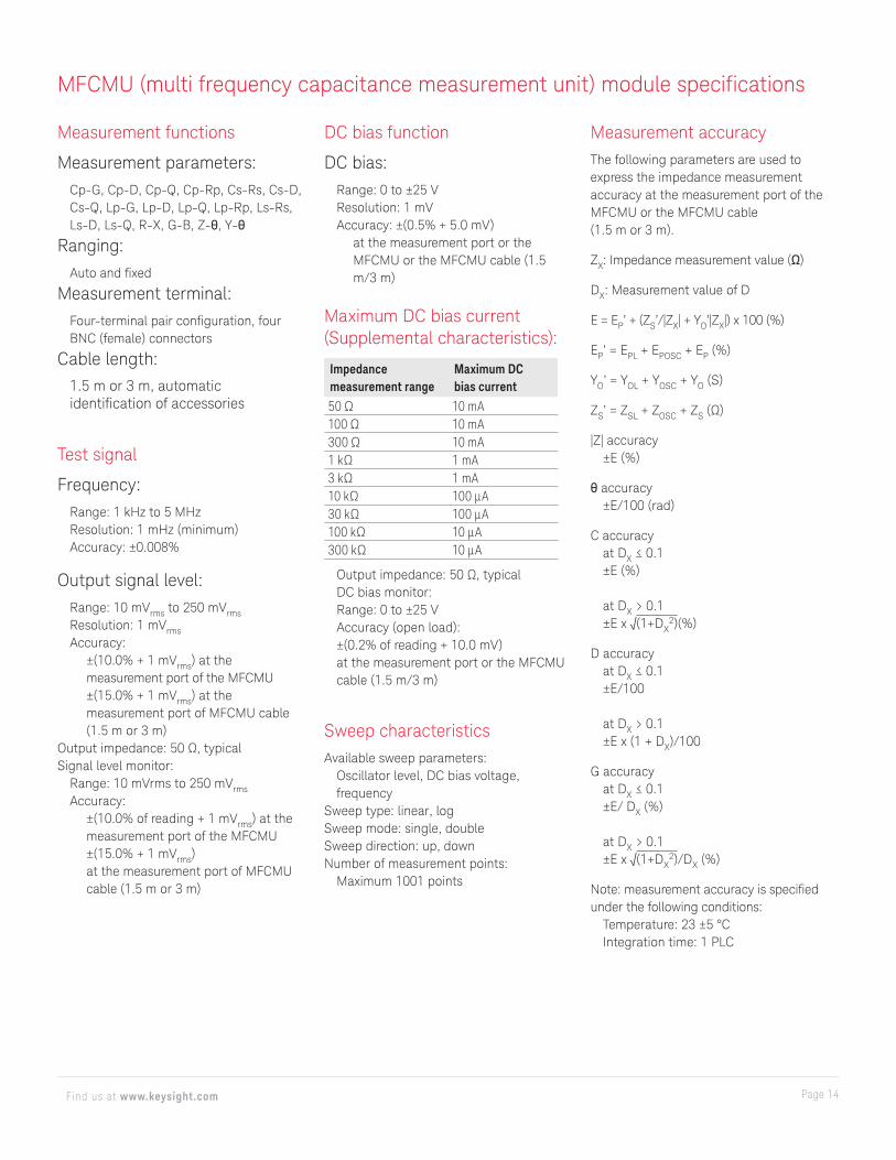
UHCU:
Output peak power
Current range
Peak power
± 500 A 7.5 kW± 1500 A 22.5 kW
Voltage range, resolution, and accuracy
Voltage range Setting resolution Measure resolution Setting accuracy1.2,3 ±(% + mV)
Measure accuracy1,3 ±(% + mV)
± 60 V 200 µV 100 µV ±(0.2 + 10) ±(0.2 + 10)1. ±(% of reading value + fixed offset in mV) 2. Setting accuracy is defined at open load.3. Accuracy is defined 1 ms pulse width at 500 A range and 500 μs pulse width at 1500 A range.
Current range, resolution, and accuracy1
Current range Setting resolution Measure resolution Setting accuracy2,3
±(% + A + A)Measure accuracy2,3
±(% + A + A)
± 500 A 1 mA 500 µA ±(0.6 + 0.3 + 0.01*Vo) ±(0.6 + 0.3 + 0.01*Vo)
± 1500 A 4 mA 2 mA ±(0.8 + 0.9 + 0.02*Vo) ±(0.8 + 0.9 + 0.02*Vo)
1. Maximum voltage compliance in current pulse mode is 63 V. Over 400 A at 500 A range and over 1200 A at 1500 A range are supplemental characteristics. 2. Accuracy is defined with 1 ms pulse width at 500 A range and with 500 μs pulse width at 1500 A range.3. ±(% of reading value + fixed offset in A + proportional offset in A), Vo is the Output Voltage.
UHCU Pulse width and resolution
Current range Voltage pulse width Current pulse width Resolution Pulse period1
500 A 10 μs – 1 ms 10 μs – 1 ms 2 μs Duty ≤ 0.4%
1500 A 10 μs – 500 μs 10 μs – 500 μs 2 μs Duty ≤ 0.1%
1. At continuous maximum current output, the output current may be reduced due to insufficient charging time.

Page 25Find us at www.keysight.com
UHC measurement and output range
The UHCU output is only available in pulsed mode.
In the equations in the above diagram, ‘I’ stands for current, ‘V’ for Voltage.
The maximum current is defined when the output terminals are shorted.
Also, the maximum current is limited by the residual resistance of the test leads, by by contact resistance between the internal jumper cable and the DUT and by the DUT impedance.
Other functionality Fiilter Filter can be used for UHC output in current mode at 500 A range.Thermocouple input: 2 ea Two K-type thermocouple inputs Temperature range: -50 °C to 300 °C.
Other Terminals/IndicatorsDigital I/O input: 1 ea.Digital I/O output: 1 ea.Power indicator: 1 ea.High voltage indicator: 1 ea.Selector indicator: 1 ea. Interlock terminal: 1 ea.Earth terminal: 1 ea.Wrist strap terminal: 1 ea.
UHCU Output resistance
Output range Nominal value
500 A 120 mΩ
1500 A 40 mΩ
Supplemental characteristics
Leakage Selector channel HVSMU is applied at High Sense terminal: less than 1 nA HPSMU/MPSMU is applied at High Force terminal: less than 10 nA
UHVU channel Less than 1 nA
SMU channel Less than 1 nA
Thermocouple reading accuracy
Temperature range Accuracy
0 °C ≤ T < 100 °C ±2 °C
T ≥ 100 °C ±5 °C
T < 0 °C ±5 °C
60-60
500
-500
1500
-1500
Current (A)
Voltage (V)
I = (60 -V)/ 0.04
I = (60 -V)/ 0.12
I = (-60 -V)/ 0.04
I = (-60 -V)/ 0.12
Measurement and output range for 1500 A range
Measurement and output range for 500 A range

Page 26Find us at www.keysight.com
HVSMU Current Expander (N1266A) Specifications
Specifications
Functions:Current expander capability Expands HVSMU current up to 2.5 A. Current expansion is made using the High Voltage Medium Current Unit (HVMCU), which is comprised of a module in the N1266A, HVSMU and two MCSMUs.
Selector capabilityThis allows the connections between the output terminal to be switched between the HVMCU and the HVSMU. The HVSMU output can be routed either directly or through a 100 kΩ resistor.
Output Terminals: High (HV Triaxial) Low (BNC)
Maximum output: HVSMU : ±3000 V/4 mA, ±1500 V/8 mA HVMCU : Refer to HVMCU specification
Output Peak Power
Voltage range Peak power
± 2200 V 600 W
± 1500 V 900 W
HVMCU
Voltage range, resolution, and accuracy
Voltage range Setting resolution Measure resolution Setting accuracy1, 2, 3
±(% + V)Measure accuracy1, 2
±(% + V)
± 2200 V 3 mV 3 mV ±(5 + 20) ±(0.8 + 1.8)
± 1500 V 1.5 mV 3 mV ±(5 + 20) ±(0.8 + 1.8)
1. ±(% of reading value + fixed offset in V)2. Accuracy is defined with 100 μs pulse at 1.1 A range and 2.5 A range, 1 ms pulse at 100 mA range.3. Setting accuracy is defined at open load.
Current range, resolution, and accuracy1, 2
Current range Measure resolution Measure accuracy1
±(% + A + A)
± 2.5 A 4 µA ±(0.9 + 4E-3 + Vo x 3E-7)
± 1.1 A 4 µA ±(0.9 + 4E-3 + Vo x 3E-7)
± 110 mA 200 nA ±(0.9 + 2E-4 + Vo x 3E-7)
1. Supplemental characteristics over 1.1 A.2. Applicable condition: 20 averaging samples

Page 27Find us at www.keysight.com
Other Terminals / Indicators Digital I/O Input: 1 ea.Digital I/O output: 1 ea.Power indicator: 1 eaSelector indicator: 1 ea
Output resistance
Output range Nominal value
1500 V / 2.5 A 600 Ω
2200 V / 1.1 A 2000 Ω
2200 V / 110 mA 20000 Ω
Supplemental characteristics
HVMCU Pulse width and resolution
Output range Pulse width Resolution
1500 V / 2.5 A 10 μs – 100 μs 2 μs
2200 V / 1.1 A 10 μs – 100 μs 2 μs
2200 V / 110 mA 10 μs – 1 ms 2 μs
HVMCU Measurement and output range
The HVMC’s output is only available in pulsed mode.
In the equations in the above diagram, ‘I’ stands for current, ‘V’ for Voltage.
The maximum current is defined when the output terminals are shorted.
Also, the maximum current is limited by the residual resistance of the test leads, by contact resistance between the internal jumper cable and the DUT and by the DUT impedance.
HVMCU Charged Capacitance: 0.22 μF
Leakage Selector output HVSMU: less than 300 pA
2200
-2200
1.1
-1.1
2.5
-2.5
Current (A)
Voltage (V)
1500
-1500
I = (1500 -V)/ 600
I = (2200 -V)/ 2000
I = (-1500 -V)/ 600
I = (-2200 -V)/ 2000
Measurement and output range

Page 28Find us at www.keysight.com
UHV (Ultra High Voltage) Expander (N1268A) Specifications
SpecificationsVoltage range, resolution, and accuracy1
Voltage range Force resolution Measure resolution Setting accuracy2, 3
±(% + V)Measure accuracy2
±(% + V)
± 10 kV 10 mV 10 mV ±(1.2 + 42) ±(1.2 + 42)
1. N1268A is controlled and makes measurement with two MCSMUs or a combination of a HCSMU and a MCSMU. 2. ±(% of reading value + fixed offset in V)3. Setting accuracy is defined at open load.
Current range, resolution, and accuracy1
Current range Measure resolution Measure accuracy2 ±(% + A + A)
± 10 µA 10 pA ±(0.06 + 2E-9 + 1E-9)
± 100 µA 100 pA ±(0.06 + 2E-8 + 1E-9)
± 1 mA 1 nA ±(0.06 + 2E-7 + 1E-9)
± 10 mA 10 nA ±(0.06 + 2E-6 + 1E-9)
± 100 mA3 100 nA ±(0.06 + 20E-6 + 1E-9)
1. N1268A is controlled and makes measurement with two MCSMUs or a combination of a HCSMU and a MCSMU. 2. ±(% of reading value + fixed offset in A + fixed offset in A)3. Pulsed mode only (Maximum pulse width is 1 ms). The maximum current is 20 mA.
UHV measurement and output range
Pulse only
DC and pulse
10000
-10000
0.01
-0.01
0.02
-0.02
Current (A)
Voltage (V)
Pulse only
DC and pulse
Other Terminals / Indicators Digital I/O Input: 1 ea.Power indicator: 1 eaHigh Voltage indicator: 1 eaInterlock terminal Input: 1 eaInterlock terminal Output: 1 eaEarth terminal: 1 ea
UHVU Output resistance
Output range Nominal value
High 10000 Ω
Low 1000 Ω
Supplemental characteristics
Other AC characteristics
Slew rate 100 V/µs (with 1 m cable)
Overshoot ±1% of setting voltage
Ripple 3 Vp-p
Maximum load capacitance 5 nF
Maximum load inductance 5 µH
UHV Pulse width and resolution
Output range Pulse width Resolution
100 mA 100 µs to 1 ms
2 µs
≤ 10 mA 100 µs to 2 s 2 µs
Output TerminalsHigh : UHV coaxialLow : SHV
Pulse PeriodMin: 10 msMax: 5 s
Page 29Find us at www.keysight.com
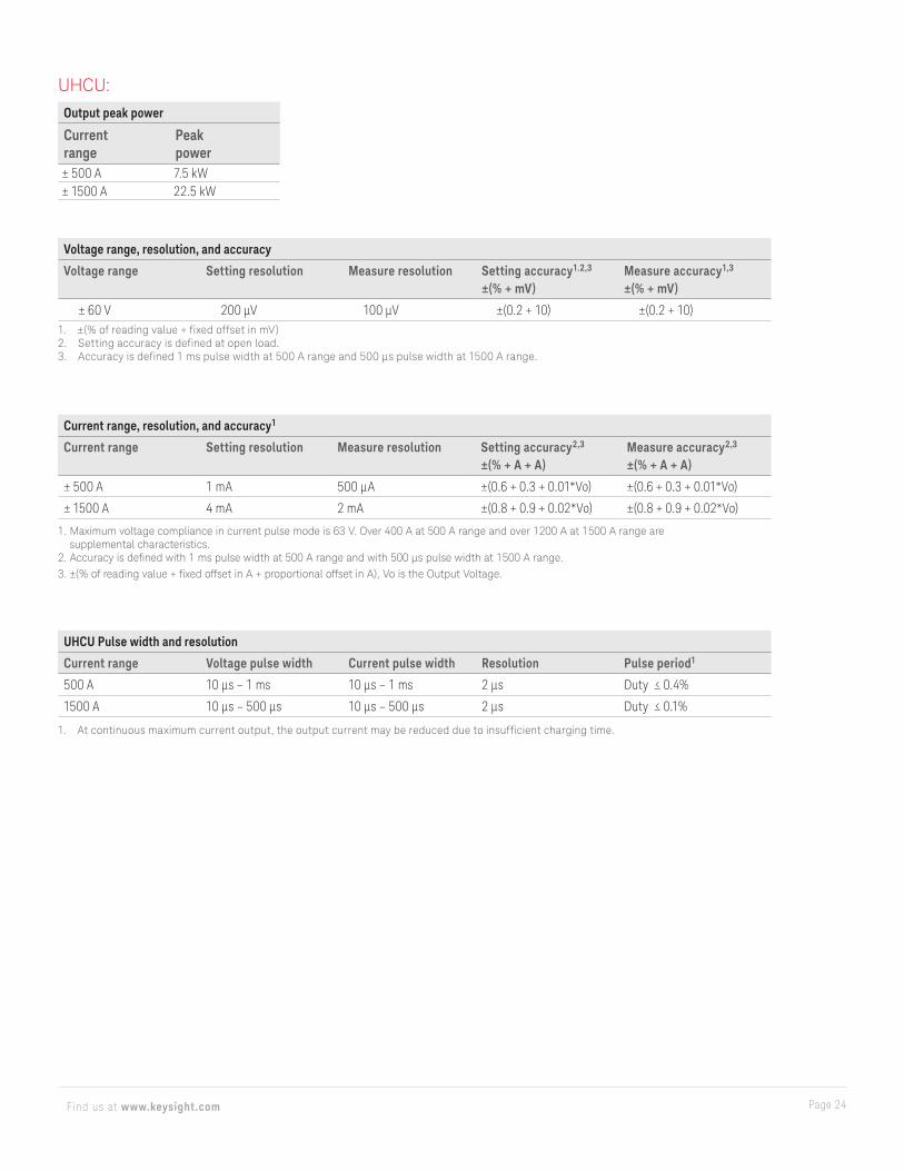
Gate charge measurement specifications
Qgate (C)
QgdQgs
Qgs1
Qg
Qgs2
Vth
Vgspleteau
Vgs
Vgs(V)
The B1505A can perform gate charge characterization for Nch MOSFETs and IGBTs. Both packaged devices and on-wafer devices are supported. The following table shows the available solutions and their required accessories (which depend on device type and current level). Temperature dependent measurements using a Thermostream or the Thermal plate are not supported.
Qg: Gate chargeQgs: Gate-source chargeQgs1: Gate charge at thresholdQgs2: Gate charge from threshold to onset of plateauQgd: Gate-drain charge
Package solution On-wafer solution
Hardw
are configuration
High voltage module B1513B/C HVSMU
Max voltage range 3000 V
High current module B1512A HCSMU N1265A-500 N1265A-1500A B1512A HCSMU
N1265A-500A N1265A-1500A
Max current range 20 A 500 A 1500 A 20 A 500 A 1500 A
Gate control module B1514A MCSMU
Ireg control module B1514A MCSMU
Fixture/selector N1259A N1265A N1258A N1265A
Adapter/selector N1259AU-014 N1265AU-014 N1274A N1275A
Measurem
ent parameter
Qg 1 nC to 100 µC
Min resolution 10 pC
Vds (vce) @high voltage
0 V to +3000 V
Voltage/sampling resolution 3 mV / 6 us
Vds(vce) @ high current
Not Support -60 V to 60 V Not Support -60 V to 60 V
Voltage /sampling resolution 100 µV / 2 µs 100 µV / 2 µs
Id (ic) maximum rated current 20 A1 350 A1 500 A1,2 20 A1 350 A1 500 A1,2
Current/sampling resolution 2 mA / 2 µs
Vgs (vge) -30 V to +30 V
Voltage/sampling resolution 40 µV / 2 µs
Ig 10 nA to 1 A
Current/sampling resolution 10 pA / 2 µs
Hardware configuration and measurement/setting parameters

Page 30Find us at www.keysight.com
Package solution On-wafer solution
Setting parameters
Vds (vce) @high voltage 0 V to +3000 V
Resolution 3 mV
Vds(vce) @ high current -20 to 20 V1 -60 to 60 V -40 to 40 V1 -60 to 60 V
Resolution 20 µV 100 µV 40 µV 100 µV
Id max 20 A1 450 A1 1100 A1,2 20 A1 350 A1 500 A1
Gate drive vgs(vge) -30 to +30 V
Resolution 40 µV
Gate control current ig 1 µA to 1 A
Resolution 0.1 µA
Current regulator control voltage
-30 to +30 V
Resolution 40 µV
On time 50 - 950 µs 50 - 950 µs 50 - 950 µs 50 - 950 µs
Resolution 2 µs
Target devices:
Nch MOSFETs and IGBTs in TO package, in modules and on-waferNote that Pch MOSFETs are not supported.
1. The maximum current will be reduced by the series resistance of the current source, residual resistance in the measurement path, and the DUT impedance.
2. The gate charge measurement adapter also has a maximum current limit of 500 A.
Hardware configuration and measurement/setting parameters (continued)

Page 31Find us at www.keysight.com
N1267A High Voltage Source Monitor Unit / High Current Source Monitor Unit Fast Switch
FeaturesThe N1267A supports fast switching between the HVSMU and HCSMU to enable the measurement of the Gallium Nitride current collapse effect.
The N1267A switch requires one MCSMU in the B1505A mainframe for control. The gate of the DUT (Device Under Test) can be driven by either an MCSMU or an HCSMU.
Note #1: The N1267A can only be used with the B1513B or B1503C HVSMU; it cannot be used with the B1513A HVSMU.Note #2: The N1267A does not support the two HCSMU 40 A configuration. Note #3: The N1267A does not support the N1265A test fixture/current expander.
SpecificationsInput terminals:HVSMU port, 1 ea (HV triaxial)HCSMU port, 1 ea (Force: BNC, Sense: Triaxial)MCSMU port, 1 ea (Force/Sense: Triaxial)GND port, 1 ea (Triaxial)Output terminals: High (HV triaxial), Low (BNC)Maximum current: 20 AMaximum voltage: 3000 V
Measurement modeGaN Current collapse (Dynamic I-V) measure mode 1. I-V time domain measurement 2. I-V trace measurementStatic characteristics mode 1. Id-Vds, Vf-If measurement 2. Id(off)-Vds, Vr-Ir measurement
Source and Measure Range

Page 32Find us at www.keysight.com
HVSMU Source setting range for OFF-state
Voltage Current
+1 V - +3000 V 1 4 mA (V > 1500 V), 8 mA (V ≤ 1500 V)
GaN current collapse measure modeTo make the GaN current collapse measurement, the HVSMU first applies high voltage stress to the DUT when the DUT is in the OFF-state. Next the HVSMU performs voltage measurement and the HCSMU performs I-V measurement to monitor the ON-state characteristics of the DUT. When making the ON-state measurement, the HVSMU is measuring voltage and both the HVSMU and HCSMU are used to measure the total current.
1 Setting value must be the ON state voltage plus 1 V or more.
HCSMU source setting range for ON-state
Voltage Current
0 V - ±40 V 2Maximum Minimum
20 A pulse (V ≤ 20V) / 1 A DC 20 mA 3
2 Voltage actually applied to the device under test (DUT) is the setting value minus the voltage drop of the switch.3 Sum of HCSMU output current and HVSMU output current flow into DUT.
Minimum voltage measurement resolution for OFF-state: 200 µVMinimum current measurement resolution for ON-state: 100 nAMinimum transition time (OFF to ON): 20 µsDuration setting for OFF-state: 10 ms - 655.35 sSampling rate: 2 µs to 12 µs for current, 6 µs for voltageMinimum ON state duration: 50 µs
Static characteristics modeThe following information applies to measurement of the DUT ON-state static characteristics. The N1267A ensures that the DUT is in the ON-state during these measurements. The HVSMU applies 0 V with 1 µA compliance and measures Vds or Vf. At the same time, the HCSMU is also performing an I-V measurement. The Id or If is determined by adding together the total current measured by both the HCSMU and the HVSMU.
HCSMU source setting for Id-Vds, Vf-If measurement
Voltage Current
0 V - ±40 VMaximum Minimum
20 A pulse (V ≤ 20V) / 1 A DC 20 mA 4
4 Offset error for the Id-Vds, If-Vf measurement is typical 1 µA
Minimum voltage measurement resolution: 200 µVMinimum current measurement resolution: 10 pA 4)
The following information applies to measurement of the DUT OFF-state static characteristics. The N1267A ensures that the DUT is in the OFF-state during these measurements. The HCSMU applies 0 V. At the same time, the HVSMU performs I-V measurement and measures Vds or Vr. The Id(Off) or Ir is determined by adding together the total current measured by both the HCSMU and the HVSMU.
HVSMU source setting for Id(off)-Vds, Vr-Ir measurement
Voltage Current
0 V - +3000 V Maximum Minimum
4 mA (V > 1500 V), 8 mA (V ≤ 1500 V)
10 µA 5
5 Leak error for the Idss, Ir-Vr measurement is typical 2 nA.
Minimum voltage measurement resolution: 200 µVMinimum current measurement resolution: 10 pA 5)
Page 33Find us at www.keysight.com
N1258A module selector
SpecificationsInput terminals:
HPSMU force port1, 1 ea., (Triaxial)HPSMU sense port1, 1 ea., (Triaxial)HCSMU force port, 1 ea. (BNC)HCSMU sense port, 1 ea. (Triaxial)HVSMU port2, 1 ea. (HV triaxial)GNDU port, 1 ea. (Triaxial)Digital I/O port, 1 ea. (D-sub 25 pin)AC power line connector, 1 ea. 1. Either HPSMU or MPSMU can be connected to HPSMU port.2. Either HVSMU or HVMCU can be connected to HVSMU port.
Output terminal:High force (HV triaxial)High sense (HV triaxial)Low force (BNC)Low sense (BNC)External relay control output (D-sub 15 pin)
Protection:HPSMU, GNDU, HCSMU Low Force
Power indicator:LED turns yellow when AC power is applied and turns green the module selector is ready to use.
Status indicator:Green LED lights to indicate the present connection path of module selector; Open, HCSMU, HPSMU, or HVSMU.
Maximum voltage/current:For HPSMU port:
±200 V/1 AFor HCSMU port:
±40 V/2 A, ±20 V/30 A (Pulse width 1 ms, duty 1%)
For HVSMU port:±3000 V/4 mA, ±1500 V/2.5 A, ±2200 V/1.1 A
Supplemental characteristicsLeakage current:
For HPSMU:40 pA at 200 V
For HCSMU:100 pA at 10 V (High Force to Low Force, High Sense to Low Sense)
For HVSMU:300 pA at 3000 V (humidity range: 20% to 50% RH)
N1259A test fixture
SpecificationsInput terminals:
HPSMU port1, 2 ea.Force, sense (Triaxial)
HCSMU port, 2 ea.Force (BNC), sense (Triaxial)
HVSMU port2, 1 ea. (HV triaxial)GNDU port, 1 ea. (Triaxial)AUX port, 2 ea. (BNC)Interlock port, 1 ea.
1. Either HPSMU or MPSMU can be connected to HPSMU port.2. Either HVSMU or HVMCU can be connected to HVSMU port. Protection:
HPSMU, GNDU, HCSMU Low Force terminal
High voltage indicator:LED turns red when a SMU output voltage is over 42 V.
Maximum voltage/current:For HPSMU port:
Force: ±200 V/1 ASense: ±200 V
For HCSMU port:High Force: ±40 V/2 A, ±20 V/40 A (Pulse width 1 ms, duty 1%)Low Force: ±40 V/2 A, ±20 V/40 A (Pulse width 1 ms, duty 1%)High Sense: ±40 VLow Sense: ±40 V
For HVSMU port:Force: ±3000 V/4 mA, ±1500 V/2.5 A, ±2200 V/1.1 A
Note: The total power consumption of all modules cannot exceed 50 W when using test fixture under the condition that operating temperature is more than 35 °C.
Supplemental characteristicsLeakage current:
For HPSMU (Force, Sense) port:40 pA at 200 V (Force, Sense)
For HCSMU (High Force, High sense) port: 100 pA at 10 VFor HVSMU (Force) port:
300 pA at 3000 V (humidity range: 20% to 50% RH)
N1259A-010 inline package socket module (3 pin)
SpecificationsNumber of terminal:
Sockets, 6 ea. (Ø4 mm jack (banana))DUT interface:
Inline package socket (3-pin)Maximum voltage for terminals:
3000 Vdc
N1259A-011 universal socket module
SpecificationsNumber of terminal:
Sockets, 8 ea. (Ø4 mm jack (banana))Maximum voltage for terminals:
3000 Vdc
Accessories

Page 34Find us at www.keysight.com
N1259A-013 Curve Tracer test adapter socket module
SpecificationsNumber of terminals: Sockets, 6 ea. (Ø4 mm jack (banana))Test adapter interface:* Sockets, 6 ea. (Ø4 mm jack (banana))Maximum voltage at terminals: 3000 V Vdc Maximum current for terminals: For Collector/Drain Force and Emitter/Source Force 39 A (DC), 500 A (Pulse) For others 1 A (DC), 20 A (Pulse)
*A test adapter for Tektronix curve tracers (370B/371B) can be connected to this interface.
N1259A-014 Gate Charge Socket Adapter
PurposeTo make gate charge measurements with the N1259A.
Required Hardware – N1259A test fixture, 1 ea. – N1259A-300 Module selector, 1 ea. – B1512A HCSMU, 1 ea. – B1513B/C HVSMU, 1 ea. – B1514A MCSMU, 2 ea.
SpecificationsNumber of terminals: Sockets, 8 ea. (Ø4 mm jack (banana))Maximum voltage at terminals: For Gate DUT High: 30 V For Gate DUT Low: 10 V For selector force High: 3000 V For selector force Low: 10 V For selector sense High: 3000 V For selector sense Low: 10 V For SMU control High: 30 V For SMU control Low: 10 VMaximum current for terminals: For Gate DUT High:1 A For Gate DUT Low: 1 A For selector force: 500 A For selector sense: 20 mA For SMU control: 1 A
Furnished accessories – Test lead (red), short, 2 ea. – Test lead (black), short, 2 ea. – Test lead (red), long, 4 ea. – Test lead (black), long, 4 ea.
N1259A-020 high voltage bias-tee
SpecificationsInput terminals:
DC bias input, 1 ea. (Ø4 mm jack (banana))MFCMU port, 1 ea.
Hcur, Hpot, Lcur, Lpot, (BNC)Guard input, 1ea (Ø4 mm banana jack)
Output terminal:MFCMU port
High (SHV)Low (SHV)
External DC bias voltage: ±3000 VFrequency:
10 kHz to 1 MHz (150 Ω at 10 kHz)Series capacitance: 110 nF ±5%Input resistance: 100 kΩ ±1%
N1259A-021 1 MΩ resistor box
SpecificationsInput/output terminals:
Ø4 mm jack (banana), 1 ea.Resistance: 1 MΩ ±5%Maximum voltage: ±3000 VPower rating: 9 W
Supplemental characteristicsLeakage current: 10 pA at 100 V
N1259A-022 100 kΩ resistor box
SpecificationsInput/output terminals:
Ø4 mm jack (banana), 1 ea.Resistance: 100 kΩ ±5%Maximum voltage: ±3000 VPower rating: 6.4 W
Supplemental characteristicsLeakage current: 10 pA at 100 V
N1259A-030 1 kΩ resistor box for gate
SpecificationsInput/output terminals:
Ø4 mm jack (banana), 1 ea.Resistance: 1 kΩ ±10%Maximum voltage: ±200 VMaximum power: 1 W
Supplemental characteristicsLeakage current: 10 pA at 100 V
N1259A-035 Universal resistor box
SpecificationsInput/output terminals:
Ø4 mm banana jack, 1 ea.Resistance: Installed by a user Maximum voltage for terminals:
±3000 V
N1259A-300 module selector for test fixture
SpecificationsInput terminals:
HPSMU port1, 1 ea.Force, sense (Triaxial)
HCSMU port, 1 ea.Force (BNC), sense (Triaxial)
HVSMU port2, 1 ea. (HV triaxial)GNDU port, 1 ea. (Triaxial)Digital I/O port, 1 ea. (D-sub 25 pin)AC power line connector, 1 ea.
1. Either HPSMU or MPSMU can be connected to HPSMU port.2. Either HVSMU or HVMCU can be connected to HVSMU port.

Page 35Find us at www.keysight.com
Output terminal:High force and guardHigh sense and guardLow forceLow sense(Ø4 mm jack (banana))
Protection:HPSMU, GNDU, HCSMU Low Force
Power indicator:LED turns yellow when AC power is applied and turns green the module selector is ready to use.
Status indicator:Green LED lights to indicate the present connection path of module selector; Open, HCSMU, HPSMU, or HVSMU.
Maximum voltage/current:For HPSMU port:
±200 V/1 AFor HCSMU port:
±40 V/2 A, ±20 V/30 A (Pulse width 1 ms, duty 1%)
For HVSMU:±3000 V/4 mA, ±1500 V/2.5 A, ±2200 V/1.1 A
Supplemental characteristicsLeakage current:
For HPSMU:10 pA at 200 V
For HCSMU:100 pA at 10 V (High Force to Low Force, High Sense to Low Sense)
For HVSMU:10 pA at 1500 V (humidity range: 20% to 70% RH)30 pA at 3000 V (humidity range: 20% to 50% RH)
N1260A high voltage bias-tee
SpecificationsInput terminals:
HVSMU port, 1 ea. (HV triaxial)MFCMU port, 1 ea. (4 BNC, Hp, Hc, Lp, Hc)
Output terminal:H-AC Guard (SHV connector)L-AC Guard (SHV connector)
External DC bias voltage: ±3000 VFrequency:
10 kHz to 1 MHz (150 Ω at 10 kHz)Series capacitance: 110 nF ±5%Input resistance: 100 kΩ ±1%
N1261A protection adapter
N1261A-001 protection adapter for HPSMU (triaxial output)
SpecificationsInput terminals:
Force (Triaxial)Sense (Triaxial)
Output terminals:Force (Triaxial)Sense (Triaxial)
1. Either the HPSMU or the MPSMU can be connected to HPSMU port.
Supplemental characteristicsLeakage current: 10 pA at 200 V
N1261A-002 protection adapter for GNDU (BNC output)
SpecificationsInput terminals:
Force/Sense (Triaxial)Output terminals:
Force (BNC)Sense (BNC)
N1261A-003 protection adapter for HPSMU (HV triaxial output)
SpecificationsInput terminals1:
Force (Triaxial)Sense (Triaxial)
Output terminals:Force (HV triaxial)Sense (HV triaxial)
1. Either the HPSMU or the MPSMU can be connected to HPSMU port.
Supplemental characteristicsLeakage current: 10 pA at 200 V
N1261A-004 protection adapter for GNDU (SHV output)
SpecificationsInput terminals:
Force/Sense (Triaxial)Output terminals:
Force (SHV)Sense (SHV)
N1262A Resistor Box
N1262A-001 1 MΩ resistor box
SpecificationsInput terminals:
HVSMU port, 1 ea. (HV triaxial)Output terminals:
SHV connector, 1 ea.Resistance: 1 MΩ ±5%Maximum voltage: ±3000 VMaximum power: 9 W
Supplemental characteristicsLeakage current: 10 pA at 100 V
N1262A-002 100 kΩ resistor box
SpecificationsInput terminals:
HVSMU port, 1 ea. (HV triaxial)Output terminals:
SHV connector, 1 ea.Resistance: 100 kΩ ±5%Maximum voltage: ±3000 VMaximum power: 6.4 W
Supplemental characteristicsLeakage current: 10 pA at 100 V

Page 36Find us at www.keysight.com
N1262A-010 1 kΩ resistor box for gate (triaxial output)
SpecificationsInput terminals:
Triaxial connector, 1 ea.Output terminals:
Triaxial connector, 1 ea.Resistance: 1 kΩ ±10%Maximum voltage: ±200 VMaximum power: 1 W
Supplemental characteristicsLeakage current: 10 pA at 100 V
N1262A-011 1 kΩ resistor box for gate (SHV output)
SpecificationsInput terminals:
HV triaxial connector, 1 ea.Output terminals:
SHV connector, 1 ea.Resistance: 1 kΩ ±10%Maximum voltage: ±3000 VMaximum power: 1 W
Supplemental characteristicsLeakage current: 10 pA at 100 V
N1262A-020 Universal resistor box, Triaxial
SpecificationsInput terminals:
Triaxial connector, 1 ea.Output terminals:
Triaxial connector, 1 ea.Resistance: Installed by userMaximum voltage for terminals: ±200 V
N1262A-021 Universal resistor box, HV Triaxial to SHV
SpecificationsInput terminals:
HVSMU port, 1 ea. (HV triaxial)Output terminals:
SHV connector, 1 ea.Resistance: Installed by userMaximum voltage for terminals: ±3000 V
N1262A-023 Universal resistor box for Ultra High Voltage
SpecificationsInput terminals:
UHV coaxial connector, 1 ea.Output terminals:
UHV coaxial connector, 1 ea.Resistance: Installed by userMaximum voltage for terminals: ±10 kV
N1262A-036 50 Ohm Termination Adapter
SpecificationsInput terminal (BNC)Output terminal (BNC)Maximum power: 1 W
Accessories for N1265A
N1254A-524 Ultra High Current Prober System Cable
SpecificationsInput terminals: 8 ea. (Ø4 mm jack (banana)) Selector Output High Force High Sense Low Force Low Sense Guard Gate output High Force Low Force ChassisOutput terminals High Force (Ø4 mm jack (banana)) Low Force (Ø4 mm jack (banana)) High Sense (HV triaxial) Low Sense (BNC) Gate (BNC)Maximum voltage / current For High Force ±3000 V/39 A (DC), 500 A (Pulse) For Low Force ±200 V/39 A (DC), 500 A (Pulse) For High Sense ±3000 V/1 A For Low Sense, Gate ±200 V/1 A
N1265A-010 Ultra High Current 3-pin Inline Package Socket Module
SpecificationsNumber of terminal:
Sockets, 6 ea. (Ø4 mm jack (banana))DUT interface:Inline package socket (3-pin)Maximum voltage for terminals: 3000 Vdc
Maximum current for terminals: For Force 39 A (DC), 500 A (Pulse) For sense 1A (DC), 20 A (Pulse)
N1265A-011 Universal Socket Module
SpecificationsNumber of terminal: Sockets, 6 ea. (Ø4 mm jack (banana))Maximum voltage for terminals: 3000 VdcUniversal blank area : 90 mm (W) x 81 mm (D)
N1265A-013 Curve Tracer Test Adapter Socket Module
SpecificationsNumber of terminals: Sockets, 6 ea. (Ø4 mm jack (banana))Test adapter interface:* Sockets, 6 ea. (Ø4 mm jack (banana))Maximum voltage at terminals: 3000V VdcMaximum current for terminals: For Collector/Drain Force and Emitter/Source Force 39 A (DC), 500 A (Pulse) For others 1 A (DC), 20 A (Pulse)
*A test adapter for Tektronix curvetracers (370B/371B) can be connected to this interface.

Page 37Find us at www.keysight.com
N1265A-014 Gate Charge Socket Adapter
PurposeTo make gate charge measurements with the N1265A.
Required Hardware – N1265A UHC expander, 1 ea. – B1513B/C HVSMU, 1 ea. – B1514A MCSMU, 2 ea.
SpecificationsNumber of terminals: Sockets, 8 ea. (Ø4 mm jack (banana))Maximum voltage at terminals: For Gate DUT High: 30 V For Gate DUT Low: 10 V For selector force High: 3000 V For selector force Low: 10 V For selector sense High: 3000 V For selector sense Low: 10 V For SMU control High: 30 V For SMU control Low: 10 VMaximum current for terminals: For Gate DUT High:1 A For Gate DUT Low: 1 A For selector force: 500 A For selector sense: 20 mA For SMU control: 1 A
Furnished accessories – Ultra high current banana test lead,
2 ea. – Test lead (red), short, 2 ea. – Test lead (black), short, 2 ea. – Test lead (red), long, 2 ea. – Test lead (black), long, 2 ea.
N1265A-035 Universal R-Box for N1265A
SpecificationsInput: 4 ea. (Ø4 mm plug (banana)) High (Force, Sense) Low (Force, Sense)Output terminals: 2 ea. (Ø4 mm jack (banana)) High, LowResistance: Installed by a userMaximum voltage for terminals: ±200 V
N1265A-040 10 kV Ultra High Voltage Gate Protection Adapter
SpecificationsInput: 4 ea. (Ø4 mm plug (banana)) High (Force, Sense) Low (Force, Sense)Output terminals: 2 ea. (Ø4 mm jack (banana)) High, LowMaximum voltage: ±200 VMaximum surge voltage: ±10 kV
N1265A-041 Thermocouple, Type K, 2 ea
FeatureN1265A-041 can be connected to Thermocouple terminal inside the N1265A and enables B1505A to read out temperature at the top of the thermocouple.
SpecificationsConnector: Type K plugLength: 3000 mm
N1265A-045 Container for Protection Adapter and Bias Tee
FeatureN1265A-045 can accommodate protection adapters and bias tee which are used with N1265A to make the measurement envi-ronment clean and safe
SpecificationsDimension: 420 mm W x 193 mm H x 565 mm DWeight: 15 kgMaximum superimposed load: 50 kg
N1269A Ultra High Voltage Connection Adapter
FeatureTo make the connection simple and to protect measurement resources from
unexpected surge when connecting UHVU to wafer prober.
SpecificationsInput terminals: Gate MCSMU Force, 1 ea (Triaxial) Gate MCSMU Sense, 1 ea (Triaxial) Chuck MCSMU Force, 1 ea (Triaxial) Chuck MCSMU Sense, 1 ea (Triaxial) UHV Low, 1ea (HV triaxial)Output terminals: 3ea (SHV) Gate, Chuck, SourceMaximum voltage: ±200 V Maximum surge voltage: ±10 kV
N1271A Thermal test enclosure
Operation Condition Temperature: +5 °C to 30 °C Humidity: 20% to 70% RH, Non-condensingAccuracy specifications degrade by a factor of 3x versus measurements made without the thermal enclosure.(Supplemental characteristics)
Common furnished accessories: 200 mm high current cable, 2 ea. 300 mm high current cable, 2 ea. 200 mm normal cable, 6 ea. 300 mm normal cable, 4 ea. Banana pin adapter, 14 ea. Mini alligator clip, 10 ea.
Large clip, 4 ea.
N1271A-001 Thermal plate compatible enclosure for N1259A/N1265A
PurposeSupports placement of the inTEST Thermal Plate within the test fixtures (N1259A/N1265A) to enable temperature dependen-cy measurements up to 250 °C.
The inTest thermal plate with GP-IB control option is necessary for automated thermal measurement.

Page 38Find us at www.keysight.com
N1271A-002 Thermostream compatible enclosure for N1265A (3 kV IV)
PurposeTo enable thermal testing by creating an interface between the N1265A and an inTEST Thermostream. The enclosure supports fully automated IV temperature measurements from -50 °C. to +220 °C.
SpecificationsAccuracy specifications degrade by a factor of 3x versus measurements made without the thermal enclosure.(Supplemental characteristics)
Number of channelsSMU: 6 (When using non-Kelvin connections), 3 (When using Kelvin connections) Gate: 1 Selector output: 1
N1271A-005 Thermostream compatible enclosure for N1265A (3 kV IV, CV & 10kV)
PurposeTo enable thermal testing by creating an interface between the N1265A and an inTEST Thermostream. The enclosure supports fully automated IV and CV measurements up to 3 kV, and IV measurements up to 10 kV at temperature ranging from -50 °C. to +220 °C.
SpecificationsAccuracy specifications degrade by a factor of 3x versus measurements made without the thermal enclosure.(Supplemental characteristics)
Number of channelsSMU: 4 (When using non-Kelvin connections), 2 (When using Kelvin connections) Gate: 1 Gate with protection resistor for UHV: 1Selector output: 1UHV: 1Capacitance: 1
N1273A Capacitance Test Fixture
PurposeTo enable packaged device capacitance testing in conjunction with the N1272A Device Capacitance Selector. SpecificationsInput terminals: Collector/Drain (SHV) 3000 V 20 mA Base/Gate (SHV) 100 V 100 mA Emitter/Source (SHV) 100 V 120 mA AC/DC Guard (SHV) 3000 V 100 mA Interlock port, 1 ea. Earth terminal
High voltage indicator: LED turns red when a SMU output is over 42V.Maximum voltage for SHV port: 3 kV
Furnished accessories – System cable between selector and
test fixture (SHV x 4, Interlock, Earth), 1 ea.
– 3-pin Inline Package Socket Module, 1 ea
– 200 mm normal cable, 4 ea. – Banana pin adapter, 4 ea. – Mini alligator clip, 4 ea. – M5 8 mm Torx pan head screw, 2 ea.
N1273A-011 Universal Socket Module
SpecificationsNumber of terminals: Sockets, 6 ea. (O4 mm jack (banana))Maximum voltage for terminals: 3 kVFurnished accessories: Test wire for thermal test (2 m) Lag connectors x 14 Screws
N1273A-013 Curve Tracer Test Adapter Socket Module
SpecificationsNumber of terminals: Sockets, 6 ea. (O4 mm jack (banana))(Sense terminals of this adapter are open. Only force terminals are connected to output terminals of N1273A.)Maximum voltage for terminals: 3 kV 100 mA*A test adapter for Tektronix curve tracers (370B/371B) can be connected to this interface.
N1274A On-Wafer Gate Charge measurement adapter/selector for 20 A/3 kV
PurposeTo enable gate charge measurements on-wafer using the HCSMU (20 A) and HVSMU (3 kV).Note: The connection changes to switch between IV measurement and gate charge measurement are automatically performed via high voltage/high current switches in the N1258A module selector and relays in the N1274A.
Required HardwareThe following modules and accessories are required in addition to the N1274A.
N1258A Module selectorB1512A HCSMUB1513B/B1513C HVSMUB1514A MCSMU x 2Current control MOSFET/IGBT
SpecificationsInput terminals (Connector) [Maximum voltage/current]: – Current control MCSMU Force
(Triaxial) [±30 V/1 A] – Current control MCSMU Sense
(Triaxial) [±30 V/1 A] – DUT Gate control MCSMU/HCSMU
Force (Triaxial) [±30 V/1 A] – DUT Gate control MCSMU/HCSMU
Sense (Triaxial) [±30 V/1 A]

Page 39Find us at www.keysight.com
– High Force (HV triaxial) [±3 kV/20 A] – High Sense (HV triaxial) [±3 kV/20 A] – Low Force (BNC) [±40 V/20 A] – Low Sense (BNC) [±40 V/1 A] – Relay control port (D-sub 15 pin)
Output terminal (Connector) [Maximum voltage/current]: – High Force (banana) [±30 V/1 A] – High Sense (HV triaxial) [±30 V/1 A] – Low Force (banana) [±30 V/1 A] – Low Sense (banana) [±30 V/1 A] – Gate (BNC) [±40 V/20 A]
Supplemental characteristicsDC leakage:
– 1 nA at 3000 V (for HVSMU) – 1 nA at 100 V (for MPSMU) – 1 nA at 200 V (for HPSMU) – 1 nA at 40 V (for HCSMU)
Furnished cables – HCSMU cable 30 cm, 2 ea. – HVSMU cable 35 cm, 1 ea. – HVTraiaxial plug coax cable 35 cm, 1
ea. – Relay control cable 30 cm, 1 ea.
N1275A On-Wafer Gate Charge measurement adapter for N1265A
PurposeTo enable on-wafer gate charge measurements with the UHCU (500 A) and HVSMU (3 kV)
Note: Unlike the N1274A, switching between IV and Qg requires manual connection changes.
Required HardwareThe following modules and accessories are required in addition to the N1274A.
– N1265A Ultra High Current Expander – N1254A-524 Prober System Cable – B1513B/B1513C HVSMU – B1514A MCSMU x 2 – Current control MOSFET/IGBT
SpecificationsInput terminals (Connector) [Maximum voltage/current]: – Current control MCSMU Force
(Triaxial) [±30 V/1 A] – Current control MCSMU Sense
(Triaxial) [±30 V/1 A] – High Force from N1254A Opt524
(banana) [±60 V/500 A] – Low Sense from N1254A Opt524
(BNC) [±10 V/1 A] – Output terminal (Connector)
[Maximum voltage/current]: – High Force to DUT (banana)
[±60 V/500 A] – Low Sense to DUT (banana)
[±10 V/1 A] – Gate (BNC) [±40 V/20 A]
Furnished cables – Ultra high current banana to banana
cable (30 cm), 1 ea. – BNC cable (30 cm), 1 ea.
Keysight EasyEXPERT group+ Software
Keysight EasyEXPERT group+ GUI based characterization software is available either on the B1505A’s embedded Windows 10 platform with 15-inch touch screen or on your PC to accelerate the characterization tasks. It supports efficient and repeatable device characterization in the entire characterization process from measurement setup and execution to analysis and data management either interactive manual operation or automation across a wafer in conjunction with a semiautomatic wafer prober. EasyEXPERT group+ makes it easy to perform complex device characterization immediately with the hundreds of
ready-to-use measurements (application tests) furnished, and allows you the option of storing test condition and measurement data automatically after each measurement in a unique built-in database (workspace), ensuring that valuable information is not lost and that measurements can be repeated at a later date. Finally, EasyEXPERT has built-in analysis capabilities and a graphical programming environment that facilitate the development of complex testing algorithms.
Key features – Multiple measurement modes for quick
setup and measurement execution (application test, classic test, tracer test, quick test and oscilloscope view)
– Graphical display, automated analysis capabilities and data generation to Excel and image for analysis and reporting
– Built-in database (workspace) records test data automatically and simplifies the data management without numerous data files
– GUI-based self-test, self-calibration and diagnostics menu for hardware maintenance
– EasyEXPERT group+ remote control function supports the remote measurement execution of application tests that are created on GUI interactively, via the LAN interface
– Data back capability and various data protection feature for shared usage by multiple users
– Characterization environment is available either on mainframe (embedded Windows 10) or on user’s PC as a personal and portable analyzer environment. EasyEXPERT group+ can be installed on any PC as many as needed without additional charge.
Device Type Application Tests
Power MOSFET (Si, GaN) Id-Vds, Rds-Id, Id-Vgs, Vth, Cgs, Cds, Cgd, Current collapse, Breakdown, QSCV, etc.
IGBT Ic-Vce, Ic-Vge, Vth, Cge, Cce, Cgc, Breakdown, etc.
SiC, Ga2O3 Id-Vds, Rds-Id, Id-Vgs, Vth, Cgs, Cds, Cgd, Breakdown, QSCV, etc.
Power BJT Ic-Vce, Vce(sat), Ic-Vcbo, Ic-Vceo, Ie-Vbeo, etc.
Power Diode If-Vf, Ir-Vr, Cj-Vr, etc.
Capacitor C-V, C-f, C-t, Ieak-V, Breakdown, TDDB, etc.
And more And more

Page 40Find us at www.keysight.com
Oscilloscope viewThe oscilloscope view (available in tracer test mode) displays measured current or voltage data versus time. The pulsed measurement waveforms appear in a separate window for easy verification of the measurement timings. This function is useful for verifying waveform timings and debugging pulsed measurements. The following modules are supported in this view: HCSMU, MCSMU, HVSMU, UHCU, HVMCU, and UHVU. The oscilloscope view can display the pulsed waveform timings at any (user specified) sweep step of the sweep output.
Sampling interval: 2 μs (HCSMU/MCSMU/UHCU/ HVMCU/UHVU) 6 μs (HVSMU)
Sampling points: 2000 Sa (HCSMU/MCSMU/ UHCU/HVMCU/UHVU) 4000 Sa (HVSMU)
Marker function: Read-out for each data channel Resolution: 2 μs
Data saving: Numeric: Text/CSV/XMLSS
Image: EMF/BMP/JPG/PNG
Quick test modeA GUI-based Quick Test mode enables you to perform test sequencing without programming. You can select, copy, rear-range and cut-and-paste any application tests with a few simple mouse clicks. Once you have selected and arranged your tests, simply click on the measurement button to begin running an automated test sequence.
Application libraryEasyEXPERT group+ comes with over 40 application tests conveniently organized by device type, application, and technology. You can easily edit and customize the furnished application tests to fit your specific needs. Application tests are provided for the following categories; they are subject to change without notice.
Measurement modes and functions
Operation mode:Application test mode
The application test mode provides application oriented point-and-click test setup and execution. An application test can be selected from the library by device type and desired measurement, and then executed after modifying the default input parameters as needed.
Classic test modeThe classic test mode provides function oriented test setup and execution with the same look, feel, and terminology of the 4155/4156 user interface. In addition, it improves the 4155/4156 user interface by taking full advantage of EasyEXPERT group+’s GUI features.
Tracer test modeThe tracer test mode offers intuitive and interactive sweep control using a rotary knob similar to a curve tracer. Just like an analog curve tracer, you can sweep in only one direction (useful for R&D device analysis) or in both directions (useful in failure analysis applications). Test set ups created in tracer test mode can be seam-lessly and instantaneously transferred to classic test mode for further detailed measurement and analysis.Each SMU can sweep using VAR1 (pri-mary sweep), VAR2 (secondary sweep), or VAR1’ (synchronous sweep).
Measurement modes:The Keysight B1505A supports the following measurement modes:
– IV measurement – Spot – Staircase sweep – Pulsed spot – Pulsed sweep – Staircase sweep with pulsed bias – Sampling – Multi-channel sweep – Multi-channel pulsed sweep – List sweep – Linear search1
– Binary search1
– C measurement – Spot C – CV (DC bias) sweep – Pulsed spot C – Pulsed sweep CV – C-t sampling – C-f sweep – CV (AC level) sweep – Quasi-Static CV (QSCV)
1. Supported only by FLEX commands.
Sweep measurementNumber of steps: 1 to 10001 (SMU), 1 to 1001 (CMU)Sweep mode: Linear or logarithmic (log)Sweep direction: Single or double sweepHold time: 0 to 655.35 s, 10 ms resolution
Recommended GPIB I/F
1. An 82350B/C card is highly recommended because of stability and speed. 2. USB GPIB interfaces might cause serial poll error intermittently due to the intrinsic communi-cation scheme differences. It is reported that using an even GPIB address sometimes significantly decreases the chance of the error. The NI GPIB-USB-HS is recommended for stability, and the Keysight 82357B is recommended for speed.
Interface B1505A
Keysight
82350B/C PCI 1
82357A USB 2
82357B USB 2
National Instrument GPIB-USB-HS USB 2

Page 41Find us at www.keysight.com
Delay time: 0 to 65.535 s, 100 μs resolution 0 to 655.35 s, 100 μs resolution (CV (AC level) sweep, C-f sweep)Step delay time: 0 to 1 s, 100 μs resolutionStep output trigger delay time: 0 to (delay time) s, 100 μs resolutionStep measurement trigger delay time: 0 to 65.535 s, 100 μs resolution
Sampling (time domain) measurementDisplays the time sampled voltage/current data (by SMU) versus time.
Sampling channels: Up to 10Sampling mode: Linear, logarithmic (log)Sampling points: For linear sampling: 1 to 100,001/(number of channels) For log sampling: 1 to 1+ (number of data for 11 decades)Sampling interval range: 100 μs to 2 ms, 10 μs resolution 2 ms to 65.535 s, 1 ms resolution For < 2 ms, the interval is ≥ 100 μs +20 μs x (num. of channels – 1) Hold time, initial wait time: -90 ms to -100 μs, 100 μs resolution 0 to 655.35 s, 10 ms resolution
Measurement time resolution: 100 μs
Other measurement characteristicsMeasurement control
Single, repeat, append, and stopSMU setting capabilities
Limited auto ranging, voltage/current compliance, power compliance, auto-matic sweep abort functions, self-test, and self-calibration
Standby modeSMUs in “Standby” remain programmed to their specified output value even as other units are reset for the next mea-surement.
List displayMeasurement data and calculated user function data are listed in conjunction with sweep step number or time domain sampling step number. Up to 20 data sets can be displayed.
Data variable displayUp to 20 user-defined parameters can be displayed on the graphics screen.
Automatic analysis functionOn a graphics plot, the markers and lines can be automatically located using the auto analysis setup. Parameters can be automatically determined using automatic analysis, user function, and read out functions.
Analysis functionsUp to 20 user-defined analysis func-tions can be defined using arithmetic expressions. Measured data, pre-defined variables, and read out functions can be used in the computation. The results can be displayed on the LCD.
Read out functionsThe read out functions are built-in func-tions for reading various values related to the marker, cursor, or line.
Arithmetic functionsUser functions
Up to 20 user-defined functions can be defined using arithmetic expressions.Measured data and pre-defined variables can be used in the computation. The results can be displayed on the LCD.
Arithmetic operators+, -, *, /, ^, abs (absolute value), at (arc tangent), avg (averaging), cond (conditional evaluation), delta, diff (differential), exp (exponent), integ (integration), lgt (logarithm, base 10), log (logarithm, base e), mavg (moving average), max, min, sqrt, trigonometric function, inverse trigonometric function, and so on.
1. In case of some supplemental characteristics, humidity range is defined as 20% to 50% RH
Bias hold functionThis function allows you to keep a source active between measurements. The source module will apply the specified bias between measurements when run-ning classic tests inside an application test, in quick test mode, or during a repeated measurement. The function ceases as soon as these conditions end or when a measurement that does not use this function is started.
Current offset cancelThis function subtracts the offset current from the current measurement raw data, and returns the result as the measurement data. This function is used to compensate the error factor (offset current) caused by the measurement path such as the measurement cables, manipulators, or probe card.
Time stampThe B1505A supports a time stamp function utilizing an internal quartz clock. Resolution: 100 μs
Data display, analysis and arithmetic functions
Data DisplayX-Y graph plot
X-axis and up to eight Y-axes, linear and log scale, real time graph plotting. X-Y graph plot can be printed or stored as image data to clip board or mass storage device. (File type: bmp, gif, png, emf)
Scale:Auto scale and zoom
Marker:Marker to min/max, interpolation, direct marker, and marker skip
Cursor:Direct cursor
Line:Two lines, normal mode, grad mode, tangent mode, and regression mode.
Overlay graph comparison:
Graphical plots can be overlaid.

Page 42Find us at www.keysight.com
Physical constantsKeyboard constants are stored in memory as follows: q: Electron charge, 1.602177E-19 C k: Boltzmann’s constant, 1.380658E-23 ε (e): Dielectric constant of vacuum, 8.854188E-12
Engineering unitsThe following unit symbols are also available on the keyboard: a (10-18), f (10-15), p (10-12), n (10-9), u or μ (10-6), m (10-3), k (103), M (106), G (109), T (1012) , P (1015)
Data management
Workspace (Built-in database)EasyEXPERT group+ supports the built-in database called “workspace”. Workspaces are created on a SSD, and they enable to manage and access all the measurement related data without handling numerous files. Every workspace supports the following features:
– Access to measurement capabilities and data stored in the workspace.
– Save/Import/Export measurement settings and data (application library, measurement settings, my favorite setup, and measurement data)
– Recall the setup for measurement reproduction and data for analysis
Data auto record/ auto exportEasyEXPERT group+ has the ability to automatically store the measurement setup and data within a workspace. It can also export measurement data in real time, in a variety of formats such as Excel (xls).
Import/export files
File type:
Keysight EasyEXPERT format, XML-SS format, CSV format
Data ProtectionEasyEXPERT group+ has various options to protect important data as follows.
– Password protection (workspace, test definition and my favorite)
– User level access control (engineer mode/operator mode)
Workspace back-up and portability
EasyEXPERT group+ has the ability to import/export a workspace for back-up and portability.
General specification
Temperature range Operating: +5 °C to +40 °C Storage: -20 °C to +60 °C
Humidity range1
Operating: 20% to 70% RH, non-condensing Storage: 10% to 90% RH, non-condensing Storage: 20% to 80% RH, non-condensing (N1268A)
Altitude Operating: 0 m to 2,000 m (6,561 ft) Storage: 0 m to 4,600 m (15,092 ft) 0 m to 2,000 m (6,561 ft) (N1268A)
Power requirementac Voltage: 90 V to 264 V Line Frequency: 47 Hz to 63 Hz
Maximum volt-amps (VA)B1505A: 900 VA N1258A: 65 VA N1259A-300: 35 VA N1265A: 400 VA N1266A: 60 VA N1268A: 350 VAN1272A: 70 VA
Acoustic Noise EmissionLpa < 65 dBLwa: 66 dB (Operating mode)Lwa: 73 dB (Worst case mode)
About measurement accuracyRF electromagnetic field and SMU measurement accuracy: SMU voltage and current measurement accuracy can be affected by RF electromagnetic field strengths greater than 3 V/m in the frequency range of 80 MHz to 1 GHz. The extent of this effect depends upon how the instrument is positioned and shielded.
Induced RF field noise and SMU measurement accuracy: SMU voltage and current measurement accuracy can be affected by induced RF field noise strengths greater than 3 Vrms in the frequency range of 150 kHz to 80 MHz. The extent of this effect depends upon how the instrument is positioned and shielded.
Regulatory complianceEMC:
IEC 61326-1 / EN 61326-1Canada: ICES/NMB-001 AS/NZS CISPR 11
Safety:IEC61010-1 / EN 61010-1CAN/CSA-C22.2 No. 61010-1
CertificationCE, cCSAus, RCM
DimensionsB1505A:
420 mm W x 330 mm H x 575 mm DN1258A module selector:
330 mm W x 120 mm H x 410 mm DN1259A test fixture:
420 mm W x 272 mm H x 410 mm DN1260A High voltage bias-tee:
164 mm W x 53 mm H x 125 mm DN1261A-001 HPSMU protection adapter (Triaxial output):
80 mm W x 40 mm H x 110 mm DN1261A-002 GNDU protection adapter (BNC output):
80 mm W x 40 mm H x 110 mm DN1261A-003 HPSMU protection adapter (HV triaxial output):
90 mm W x 40 mm H x 140 mm DN1261A-004 GNDU protection adapter (SHV output):
80 mm W x 40 mm H x 125 mm D

Page 43Find us at www.keysight.com
N1262A resister box:50 mm W x 40 mm H x 125 mm D
N1265A UHC expander / fixture: 420 mm W x 285mm H x 575 mm D N1266A HVSMU current expander: 420 mm W x 75 mm H x 575 mm D N1267A HVSMU / HCSMU fast switch: 202 mm W x 56 mm H x 175 mm D N1268A UHV expander: 420 mm W x 222 mm H x 482 mm DN1269A Ultra High Voltage Connection Adapter: 134 mm W x 56 mm H x 150 mm D N1271A-001 Thermal plate compatible enclosure for N1259A/N1265A 500 mm W 190 mm H 365 mm D N1271A-002 Thermostream compatible enclosure for N1265A (3kV IV) 330 mm W 340 mm H 430 mm D (Outer dimension) 284 mm W 150 mm H 195 mm D (Inner dimension) N1271A-005 Thermostream compatible enclosure for N1265A (3kV IV, CV & 10kV) 330 mm W 340 mm H 430 mm D (Outer dimension) 275 mm W 150 mm H 195 mm D (Inner dimension)N1272A: 420 mm W x 75 mm H x 575 mm D N1273A: 340 mm W x 200 mm H x 345 mm D N1274A: 330 mm W x 90 mm H x 410 mm D N1275A: 116 mm W x 78 mm H x 125 mm D
WeightB1505A (empty): 20 kg B1511B: 1.1 kgB1510A: 2.0 kgB1512A: 2.1 kgB1513C: 2.0 kg B1514A: 1.3 kgB1520A: 1.3 kgN1258A: 5.0 kgN1259A: 12.0 kgN1260A: 0.6 kgN1261A: 0.3 kgN1262A: 0.3 kg N1265A: 30 kg N1266A: 10 kg N1267A: 0.8 kg
N1268A: 18 kg N1269A: 0.4 kg N1271A-001: 4.5 kg N1271A-002: 10.5 kg N1271A-005: 10.5 kg N1272A: 9.4 kg N1273A: 0.7 kg N1274A: 3.2 kg N1275A: 0.4 kg
Furnished accessoriesMeasurement cables and adapter
Triaxial cable for HPSMU, MPSMU and MCSMU, 2 ea.HCSMU cable, 1 ea.HCSMU Kelvin adapter, 1 ea.HVSMU cable, 1 ea.
Interlock cable, 1 ea.Ground unit cable, 1 ea.Keyboard, 1 ea.Mouse, 1 ea.Stylus pen, 1 ea.Power cable, 1 ea.Product CD-ROM, 1 ea.Software entitlement document for
EasyEXPERT group+SMU number label for the B1505A installed
with SMU, 1 sheetN1258A : Digital I/O cable, 1 ea.N1259A-300 : Digital I/O cable, 1 ea.N1265A : Digital I/O cable, 1 ea.N1266A : Digital I/O cable, 1 ea.N1268A : Digital I/O cable, 1 ea., Interlock cable, 1 ea.N1272A : Digital I/O cable 1.5m, 1 ea
HVSMU cable 1.5 m, 1 ea.

Page 44Find us at www.keysight.com
Mainframe and modulesB1505A Power Device Analyzer/Curve Tracer mainframe
Configure the following modules:High power SMU (HPSMU)Medium power SMU (MPSMU)High current SMU (HCSMU)Medium current SMU (MCSMU)High voltage SMU (HVSMU)Multi frequency CMU (MFCMU)
B1505A-015 1.5 m cableB1505A-030 3.0 m cableB1505A-050 50 Hz line frequencyB1505A-060 60 Hz line frequencyB1505A-A6J ANSI Z540 compliant calibrationB1505A-UK6 Commercial calibration certificate with test dataB1505A-ABA English documentation B1505A-ABJ Japanese documentationB1500A-1CM Rackmount kit
B1505A expanders/fixturesN1259A Test fixtureN1259A-010 Inline package socket module (3 pin)N1259A-011 Universal socket moduleN1259A-012 Blank PTFE boardN1259A-013 Curve Tracer test adaptor socket moduleN1259A-014 Gate Charge socket adapterN1259A-020 High voltage bias-teeN1259A-021 1 MΩ Resistor boxN1259A-022 100 kΩ Resistor boxN1259A-030 1 kΩ Resistor box for gateN1259A-035 Universal R-Box N1259A-300 Module selectorN1265A UHC expander / fixtureN1265A-010 500 A Ultra High Current 3-pin Inline Package Socket
ModuleN1265A-011 Universal Socket ModuleN1265A-013 Curve Tracer Test Adapter Socket ModuleN1265A-014 Gate Charge socket adapterN1265A-015 1500 A Current OptionN1265A-035 Universal R-Box for N1265AN1265A-040 10 kV Ultra High Voltage Gate Protection AdapterN1265A-041 Thermocouple, Type K, 2 eaN1265A-045 Container for Protection Adapter and Bias TeeN1266A High Voltage Source Monitor Unit Current Expander N1267A High Voltage Source Monitor Unit / High Current Source
Monitor Unit Fast SwitchN1268A Ultra High Voltage ExpanderN1271A Thermal Test EnclosureN1271A-001 Thermal plate compatible enclosure for N1259A/N1265A
N1271A-002 Thermostream compatible enclosure for N1265A (3kV IV)N1271A-005 Thermostream compatible enclosure for N1265A (3kV IV,
CV & 10kV)N1272A Device Capacitance SelectorN1273A Capacitance Test FixtureN1273A-011 Universal Socket ModuleN1273A-013 Curve Tracer Test Adapter Socket ModuleN1274A On-Wafer Gate Charge measurement adapter/selector
for 20 A/3 kVN1275A On-Wafer Gate Charge measurement adapter for N1265A
B1505A accessories16444A-001 Keyboard16444A-002 Mouse16444A-003 Stylus penN1253A-100 Digital I/O cableN1253A-200 Digital I/O BNC boxN1254A-100 Ground unit Kelvin adapterN1254A-101 Triaxial(m)-BNC(f)N1254A-102 Triaxial(m)-BNC(m)N1254A-103 Triaxial(m)-BNC(f)N1254A-104 Triaxial(f)-BNC(m)N1254A-105 Triaxial(f)-BNC(m)N1254A-106 Triaxial(m)-BNC(f)N1254A-107 Triaxial(m)-BNC(f)N1254A-500 HV Jack Connector (Solder Type)N1254A-501 HV Jack /Jack AdapterN1254A-502 HV plug Connector(Solder Type)N1254A-503 BNC Coax Cable Assy 1.5m(Open End)N1254A-504 HVTriax Jack Coax Cable Assy 1.5m(Open End)N1254A-505 HVTriax Plug Triax Cable Assy 1.5m (Open End)N1254A-506 HVTriax Plug Coax Cable Assy 1.5m(Open End)N1254A-507 HVTriax Plug Coax Cable Assy 1.5mN1254A-508 Test Lead cable BlackN1254A-509 Test Lead cable RedN1254A-510 Dolphin clip 2 ea. (red and black)N1254A-511 Cable lag adapter 2 ea. (red and black)N1254A-512 SHV Cable Assy 250 mmN1254A-513 SHV to BananaN1254A-514 BNC-Plug PlugN1254A-515 BNC-Jack-Plug-JackN1254A-516 BNC-Jack-Jack-JackN1254A-517 Adapter, Trixial Jack to Triaxial Plug N1254A-518 SHV Cable 1.5 mN1254A-520 10 kV Ultra High Voltage Open End Cable, 1 m.N1254A-521 10 kV Ultra High Voltage Jack to Jack AdapterN1254A-522 1500 A Ultra High Current Banana to Banana Cable, 2 ea.N1254A-523 1500 A Ultra High Current Banana to Open End Cable, 1
m, 2 ea
Order Information

This information is subject to change without notice. © Keysight Technologies, 2019, Published in USA, November 7, 2019, 5990-3853EN
Page 45Find us at www.keysight.com
Learn more at: www.keysight.comFor more information on Keysight Technologies’ products, applications or services,
please contact your local Keysight office. The complete list is available at:
www.keysight.com/find/contactus
Other accessories16493G-001 Digital I/O cable (1.5 m)16493G-002 Digital I/O cable (3 m)16493J-001 Interlock cable (1.5 m)16493J-002 Interlock cable (3 m)16493L-001 GNDU cable (1.5 m)16493L-002 GNDU cable (3 m)
Retrofit and upgrade kitsB1505AU Upgrade kit for B1505AB1505AU-001 Conversion kit from B1500A to B1505AB1500AU-PC2 Mainframe upgrade (available for S/N starts with JP or
less than MY53440000)B1500AU-PC3 Mainframe upgrade (available for S/N MY53440101 or
later)B1505AU-010 High power source monitor unit (B1510A)B1505AU-11B Medium power source monitor unit (B1511B)B1505AU-012 High current source monitor unit (B1512A)B1505AU-13C High voltage source monitor unit (B1513C)B1505AU-014 Medium current source monitor unit (B1514A)B1505AU-020 Multi frequency capacitance measurement unit (B1520A)B1505AU-SWS EasyEXPERT group+ Extension support and subscriptionN1259AU Upgrade kit for N1259AN1265AU Upgrade kit for N1265A
Package solutionB1505AP Pre-configured Power Device Analyzer/Curve Tracer
(B1505A w/ modules/fixture)B1505AP-H20 3 kV / 20 A / Fixture PackB1505AP-H21 3 kV / 20 A / C-V / Fixture PackB1505AP-H50 3 kV / 500 A / Fixture PackB1505AP-H51 3 kV / 500 A / C-V / Fixture PackB1505AP-H70 3 kV / 1500 A / Fixture PackB1505AP-H71 3 kV / 1500 A / C-V / Fixture PackB1505AP-U50 10 kV / 500 A / Fixture PackB1505AP-U70 10 kV / 1500 A / Fixture Pack
B1505A accessories (continued)N1254A-524 Ultra High Current Prober System CableN1254A-525 SHV Cable Assy 1.5m - SHV Plug To Open-endN1254A-526 Ultra High Current Cable, 2m, No Connectors At Either
EndN1254A-527 PTFE Standoff, Jack, 4 ea.N1254A-528 PTFE Standoff With Banana Plug, 4 ea.N1254A-556 Test Leads and Connection Kit for Capacitance Test, 30
cm, 4 ea.N1254A-557 Test Leads And Connection Kit For Thermal Test with
N1271AN1254A-558 SHV Cable 3mN1258A Module selectorN1260A High voltage bias-teeN1261A Protection adapterN1262A Resistor boxN1262A-020 Universal R-Box, TriaxialN1262A-021 Universal R-Box, HV Triaxial to SHVN1262A-023 Universal R-Box for Ultra High VoltageN1262A-036 50 Ohm Termination Adapter
SMU cables/accessories16493S-001 HCSMU cable (1.5 m)16493S-002 HCSMU cable (3 m)16493S-010 HCSMU Kelvin adapter16493S-011 HCSMU non-Kelvin adapter16493S-020 Dual HCSMU Kelvin combination adapter16493S-021 Dual HCSMU combination adapter16493T-001 High voltage triaxial cable (1.5 m)16493T-002 High voltage triaxial cable (3 m)16493U-001 High current BNC cable (1.5 m)16493U-002 High current BNC cable (3 m)16494A-001 Triaxial cable (1.5 m)16494A-002 Triaxial cable (3 m)16493K-001 Kelvin triaxial cable (1.5 m)16493K-002 Kelvin triaxial cable (3 m)16493V-001 10 kV Ultra High Voltage Cable, 1.5 m16493V-002 10 kV Ultra High Voltage Cable, 3 mN1269A Ultra High Voltage Connection Adapter
CMU accessoriesN1300A-001 CMU cable (1.5 m)N1300A-002 CMU cable (3 m)
Order Information (continued)