Embed Size (px)
Citation preview
AXI Interface Based ML605/SP605 MicroBlaze Processor SubsystemHardware Tutorial
UG669 (v4.1) March 12, 2012
ML605/SP605 Hardware Tutorial www.xilinx.com UG669 (v4.1) March 12, 2012
Xilinx is disclosing this user guide, manual, release note, and/or specification (the “Documentation”) to you solely for use in the development of designs to operate with Xilinx hardware devices. You may not reproduce, distribute, republish, download, display, post, or transmit the Documentation in any form or by any means including, but not limited to, electronic, mechanical, photocopying, recording, or otherwise, without the prior written consent of Xilinx. Xilinx expressly disclaims any liability arising out of your use of the Documentation. Xilinx reserves the right, at its sole discretion, to change the Documentation without notice at any time. Xilinx assumes no obligation to correct any errors contained in the Documentation, or to advise you of any corrections or updates. Xilinx expressly disclaims any liability in connection with technical support or assistance that may be provided to you in connection with the Information.
THE DOCUMENTATION IS DISCLOSED TO YOU “AS-IS” WITH NO WARRANTY OF ANY KIND. XILINX MAKES NO OTHER WARRANTIES, WHETHER EXPRESS, IMPLIED, OR STATUTORY, REGARDING THE DOCUMENTATION, INCLUDING ANY WARRANTIES OF MERCHANTABILITY, FITNESS FOR A PARTICULAR PURPOSE, OR NONINFRINGEMENT OF THIRD-PARTY RIGHTS. IN NO EVENT WILL XILINX BE LIABLE FOR ANY CONSEQUENTIAL, INDIRECT, EXEMPLARY, SPECIAL, OR INCIDENTAL DAMAGES, INCLUDING ANY LOSS OF DATA OR LOST PROFITS, ARISING FROM YOUR USE OF THE DOCUMENTATION.
© Copyright 2010–2012 Xilinx, Inc. XILINX, the Xilinx logo, Virtex, Spartan, ISE, and other designated brands included herein are trademarks of Xilinx in the United States and other countries. All other trademarks are the property of their respective owners.
Revision HistoryThe following table shows the revision history for this document.
Date Version Revision
10/05/10 1.0 Initial Xilinx release.
12/21/10 2.0 Tutorial procedures have been updated in accordance with ISE® Design Suite: Embedded Edition, version 12.4.
03/15/11 3.0 Tutorial procedures have been updated in accordance with ISE Design Suite: Embedded Edition, version 13.1.
07/06/11 4.0 Tutorial procedures have been updated in accordance with ISE Design Suite: Embedded Edition, version 13.2.
03/12/12 4.1 Updated ISE Design Suite: Embedded Edition version 13.2 to version 13.x. Updated instructions to set environment variables in note after step 5. Updated Exporting the Base Hardware Platform to SDK and References.
ML605/SP605 Hardware Tutorial www.xilinx.com 3UG669 (v4.1) March 12, 2012
Revision History . . . . . . . . . . . . . . . . . . . . . . . . . . . . . . . . . . . . . . . . . . . . . . . . . . . . . . . . . . . . . 2Introduction . . . . . . . . . . . . . . . . . . . . . . . . . . . . . . . . . . . . . . . . . . . . . . . . . . . . . . . . . . . . . . . . . 5Hardware and Software Requirements . . . . . . . . . . . . . . . . . . . . . . . . . . . . . . . . . . . . . . . 5Prerequisites . . . . . . . . . . . . . . . . . . . . . . . . . . . . . . . . . . . . . . . . . . . . . . . . . . . . . . . . . . . . . . . . . 6System Overview . . . . . . . . . . . . . . . . . . . . . . . . . . . . . . . . . . . . . . . . . . . . . . . . . . . . . . . . . . . . 6Included Files and Systems. . . . . . . . . . . . . . . . . . . . . . . . . . . . . . . . . . . . . . . . . . . . . . . . . . . 7Executing the System. . . . . . . . . . . . . . . . . . . . . . . . . . . . . . . . . . . . . . . . . . . . . . . . . . . . . . . . . 9System Design Flow . . . . . . . . . . . . . . . . . . . . . . . . . . . . . . . . . . . . . . . . . . . . . . . . . . . . . . . . 14
Hardware Platform Creation . . . . . . . . . . . . . . . . . . . . . . . . . . . . . . . . . . . . . . . . . . . . . . . 14Opening the Project . . . . . . . . . . . . . . . . . . . . . . . . . . . . . . . . . . . . . . . . . . . . . . . . . . . . 14Examining the System . . . . . . . . . . . . . . . . . . . . . . . . . . . . . . . . . . . . . . . . . . . . . . . . . . 15Generating the Hardware Platform . . . . . . . . . . . . . . . . . . . . . . . . . . . . . . . . . . . . . . . . 21
Exporting the Base Hardware Platform to SDK . . . . . . . . . . . . . . . . . . . . . . . . . . . . . . . 22Downloading and Verifying the Design . . . . . . . . . . . . . . . . . . . . . . . . . . . . . . . . . . . . . 23
Customizing the Embedded Hardware Platform . . . . . . . . . . . . . . . . . . . . . . . . . . . . . . 24Adding IP from the Xilinx IP Catalog . . . . . . . . . . . . . . . . . . . . . . . . . . . . . . . . . . . . . . . 26Adding the Perf_AXI core. . . . . . . . . . . . . . . . . . . . . . . . . . . . . . . . . . . . . . . . . . . . . . . . 28Connecting the Bus Interfaces. . . . . . . . . . . . . . . . . . . . . . . . . . . . . . . . . . . . . . . . . . . . . 29Connecting Ports. . . . . . . . . . . . . . . . . . . . . . . . . . . . . . . . . . . . . . . . . . . . . . . . . . . . . . . 33
Implementing and Downloading the Design . . . . . . . . . . . . . . . . . . . . . . . . . . . . . . . . . 35Testing the Design . . . . . . . . . . . . . . . . . . . . . . . . . . . . . . . . . . . . . . . . . . . . . . . . . . . . . . . . 35
Summary . . . . . . . . . . . . . . . . . . . . . . . . . . . . . . . . . . . . . . . . . . . . . . . . . . . . . . . . . . . . . . . . . . . 40Next Steps . . . . . . . . . . . . . . . . . . . . . . . . . . . . . . . . . . . . . . . . . . . . . . . . . . . . . . . . . . . . . . . . . . 40References . . . . . . . . . . . . . . . . . . . . . . . . . . . . . . . . . . . . . . . . . . . . . . . . . . . . . . . . . . . . . . . . . . 40
Table of Contents
ML605/SP605 Hardware Tutorial www.xilinx.com 5UG669 (v4.1) March 12, 2012
AXI Interface Based ML605/SP605 MicroBlaze Processor Subsystem Hardware Tutorial
IntroductionThis tutorial provides the steps required to build and modify the Xilinx® ML605 MicroBlaze™ Processor Subsystem or the Xilinx SP605 MicroBlaze Processor Subsystem. The tutorial starts with steps in building the basic subsystem. The basic subsystem is then modified by adding the cores necessary to measure throughput on AXI Central DMA (AXI_CDMA).
Additional information can be found in UG683, EDK Concepts, Tools, and Techniques. Readers are encouraged to refer to UG683 during the execution of this tutorial. [Ref 1]
Users should allow approximately three hours to complete this entire tutorial.
Hardware and Software RequirementsThe hardware and software requirements to run the basic tutorial are:
• Xilinx ML605 evaluation board or Xilinx SP605 evaluation board
• Two USB Type-A to Mini-B 5-pin cables
• Ethernet cable (straight-through)
• Serial communications utility program (e.g., Windows HyperTerminal or Tera Term)
• ISE® Design Suite: Embedded Edition 13.x which includes:
• Integrated Software Environment (ISE)
• Embedded Development Kit (EDK
• Software Development Kit (SDK)
6 www.xilinx.com ML605/SP605 Hardware TutorialUG669 (v4.1) March 12, 2012
Prerequisites
PrerequisitesPrerequisites required to run the basic tutorial are:
• ML605 MicroBlaze Processor Subsystem:
• Proper hardware setup and software installation, as described in UG668, Getting Started with the Virtex-6 FPGA ML605 Embedded Kit [Ref 2]
• Familiarity with the ML605 MicroBlaze Processor Subsystem, documented in DS668, AXI Interface Based ML605 Embedded Kit MicroBlaze Processor Subsystem Data Sheet [Ref 3]
• SP605 MicroBlaze Processor Subsystem:
• Proper hardware setup and software installation, as described in UG667, Getting Started with the Spartan-6 FPGA SP605 Embedded Kit [Ref 4]
• Familiarity with the SP605 MicroBlaze Processor Subsystem, documented in DS667, AXI Interface Based SP605 Embedded Kit MicroBlaze Processor Subsystem Data Sheet [Ref 5]
• Familiarity with UG683, EDK Concepts, Tools, and Techniques, Chapter 1 (Introduction), Chapter 3 (Using Xilinx Platform Studio), and Chapter 4 (Working with the Embedded Platform) [Ref 1]
• General knowledge of FPGAs, digital design concepts, and microprocessors
• Basic familiarity with the ISE Design Suite
• Basic VHDL/Verilog knowledge
System OverviewThis tutorial is based on the ML605/SP605 Embedded Kit MicroBlaze Processor Subsystem. Readers are encouraged to refer to DS668, AXI Interface Based ML605 Embedded Kit MicroBlaze Processor Subsystem Data Sheet [Ref 3] or DS667, AXI Interface Based SP605 Embedded Kit MicroBlaze Processor Subsystem Data Sheet [Ref 5] during the execution of this tutorial.
ML605/SP605 Hardware Tutorial www.xilinx.com 7UG669 (v4.1) March 12, 2012
Included Files and Systems
Included Files and SystemsThe Tutorial_Sandbox directory is a working area for this tutorial. It is provided as part of the ML605 or SP605 Embedded Kit and contains the benchmarking IP cores that are added to the base MicroBlaze Processor Subsystem to create the benchmarking system. Figure 1 shows the directory structure for the Tutorial_Sandbox working area.
Note: Although this tutorial starts from the base ML605_System, or base SP605_System as shown in Figure 1, the Tutorial_Sandbox directory contains the additional files necessary to build the benchmarking system. To generate a new tutorial sandbox, copy the Tutorial_Sandbox directory into the working area on the user’s computer.
X-Ref Target - Figure 1
Figure 1: Tutorial Sandbox Directory Structure
ML605_Embedded_Kit/SP605_Embedded_Kit
Documentation
edkBmmFile_bd.bmm
system.xml
ise_top.bit (contains no bootloop)
system.ucf
SWHW
hw_platform
hw
data
perf_axi_v1_00_a
pcores
BenchmarkDemo.elf
BenchmarkDemo
SDK_Export
Tutorial_Completed ML605_System/SP605_System
MicroBlaze_ProcessorSubSystem(XPS Project)
Tutorial_SandBox Benchmark_Demo
UG669_01_021711
board_test_platform SDK_Workspaceboard_test_app
benchmark_demostandaloneise_top.ucf
ise_proj.xise
ise_proj.gise
ise_top.vhd
8 www.xilinx.com ML605/SP605 Hardware TutorialUG669 (v4.1) March 12, 2012
Included Files and Systems
The directory structure of the completed tutorial (Tutorial_Completed) is shown in Figure 2.
X-Ref Target - Figure 2
Figure 2: Completed Tutorial Directory Structure
ML605_Embedded_Kit/SP605_Embedded_Kit
Documentation
edkBmmFile_bd.bmm
system.xml
ise_top.bit (contains no bootloop)
system.ucf
SWHW
hw_platform
hw
data
BenchmarkDemo.elf
BenchmarkDemo
SDK_Export
Tutorial_Completed ML605_System/SP605_System
MicroBlaze_ProcessorSubSystem(XPS Project)
Tutorial_SandBox Benchmark_Demo
UG669_02_021711
board_test_platform SDK_Workspace
board_test_app
hello_world_0
board_test_platform
hello_world_bsp_0
hw_platform
board_test_app
benchmark_demostandalone
perf_axi_v1_00_a
pcores
ise_top.ucf
ise_proj.xise
ise_proj.gise
ise_top.vhd
ML605/SP605 Hardware Tutorial www.xilinx.com 9UG669 (v4.1) March 12, 2012
Executing the System
Executing the SystemThe ready_for_download directory contains the pre-built bitstream and ELF files for the ML605 or SP605 MicroBlaze Processor Subsystem. The directory structure of the ML605_System is shown in DS668, AXI Interface Based ML605 Embedded Kit MicroBlaze Processor Subsystem Data Sheet [Ref 3]. The directory structure of the SP605_System is shown in DS667, AXI Interface Based SP605 Embedded Kit MicroBlaze Processor Subsystem Data Sheet [Ref 5].
The pre-built bitstream and ELF files file are used to verify that the software is properly installed and that the board is set up correctly. To execute the system using these files, follow these steps:
1. Connect a USB Type-A to Mini-B 5-pin cable between the ML605 or SP605 USB JTAG connector and the host computer.
2. Verify that the USB cable is properly connected to the USB UART connection and the host computer, as described in UG668, Getting Started with the Virtex-6 FPGA ML605 Embedded Development Kit [Ref 2], or UG667, Getting Started with the Spartan-6 FPGA ML605 Embedded Development Kit [Ref 4].
3. If the board is not already powered on, power on the ML605 board.
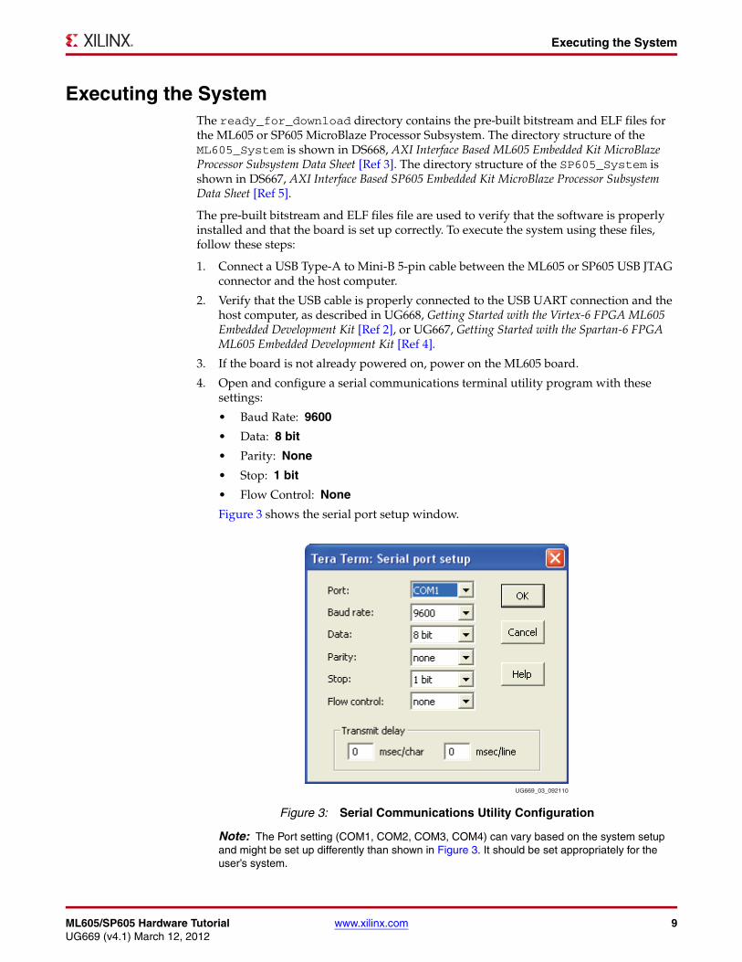
4. Open and configure a serial communications terminal utility program with these settings:
• Baud Rate: 9600
• Data: 8 bit
• Parity: None
• Stop: 1 bit
• Flow Control: None
Figure 3 shows the serial port setup window.
Note: The Port setting (COM1, COM2, COM3, COM4) can vary based on the system setup and might be set up differently than shown in Figure 3. It should be set appropriately for the user’s system.
X-Ref Target - Figure 3
Figure 3: Serial Communications Utility Configuration
UG669_03_092110
10 www.xilinx.com ML605/SP605 Hardware TutorialUG669 (v4.1) March 12, 2012
Executing the System
5. Configure and exercise the MicroBlaze Processor Subsystem by launching the Xilinx Microprocessor Debugger (XMD). Open a command shell with the proper ISE Design tool and EDK environment settings.
Note: To set environment variables, run the settings32.bat file located in the Xilinx installation area. At the command prompt, type C:\Xilinx\13.x\ISE_DS\settings32.bat (for Windows XP) or C:\Xilinx\13.x\ISE_DS\settings64.bat (for Windows 7) and press Enter.
6. Execute these commands to download the design and connect to the MicroBlaze processor:
For ML605:
$ cd ML605_Embedded_Kit/ML605_System/ready_for_download
$ xmd
XMD% fpga -f ise_top_download.bit
Note: This command downloads the hardware bitstream into the FPGA but does not download the software application.
XMD% connect mb mdm
Note: This command connects to the MicroBlaze debug module.
For SP605:
$ cd SP605_Embedded_Kit/SP605_System/ready_for_download
$ xmd
XMD% fpga -f ise_top_download.bit
Note: This command downloads the hardware bitstream into the FPGA but does not download the software application.
XMD% connect mb mdm
Note: This command connects to the MicroBlaze debug module.
7. XMD allows low-level visibility into the design. There are several useful XMD commands to allow for the peeking and poking of registers and memory locations within the system. For example, writes to and reads from the internal block RAM are done as follows:
• For ML605:
XMD% mwr 0x62000000 0xDEADBEEF
XMD% mrd 0x62000000
The value 0xDEADBEEF should be returned:
62000000: DEADBEEF
As an example of register access, write to the GPIO register which outputs data to the 8-bit GPIO LEDs on the ML605 board:
XMD% mwr 0x81420000 0xAA
The value written to this register is now reflected in the GPIO LEDs. The next write changes the LED display:
XMD% mwr 0x81420000 0x55
Note: A read from this register always returns 0x00000000, as this is an output-only register.
ML605/SP605 Hardware Tutorial www.xilinx.com 11UG669 (v4.1) March 12, 2012
Executing the System
Set all of the DIP switches labeled GPIO DIP SW (SW1) to the ON position. Then read from the GPIO register which inputs data from the DIP switches:
XMD% mrd 0x81440000
The value 0x000000FF should be returned:
81440000: 000000FF
Change the DIP switch settings and verify that the correct value is read from the GPIO register.
Note: Switch 1 is the most significant bit.
• For SP605:
XMD% mwr 0x4A000000 0xDEADBEEF
XMD% mrd 0x4A000000
The value 0xDEADBEEF should be returned:
4A000000: DEADBEEF
As an example of register access, write to the GPIO register which outputs data to the 8-bit GPIO LEDs on the SP605 board:
XMD% mwr 0x81420000 0xA
The value written to this register is now reflected in the GPIO LEDs. The next write changes the LED display:
XMD% mwr 0x81420000 0x5
Note: A read from this register always returns 0x00000000, as this is an output-only register.
Set all of the DIP switches labeled GPIO DIP SW (SW1) to the ON position. Then read from the GPIO register which inputs data from the DIP switches:
XMD% mrd 0x81440000
The value 0x0000000F should be returned:
81440000: 0000000F
Change the DIP switch settings and verify that the correct value is read from the GPIO register.
Note: Switch 1 is the most significant bit.
For more information about XMD and the commands available within XMD, see UG111, Embedded System Tools Reference Manual, Chapter 10. [Ref 6]
8. To download and execute the test software application, enter these commands at the XMD command prompt:
XMD% dow board_test_app.elf
XMD% con
12 www.xilinx.com ML605/SP605 Hardware TutorialUG669 (v4.1) March 12, 2012
Executing the System
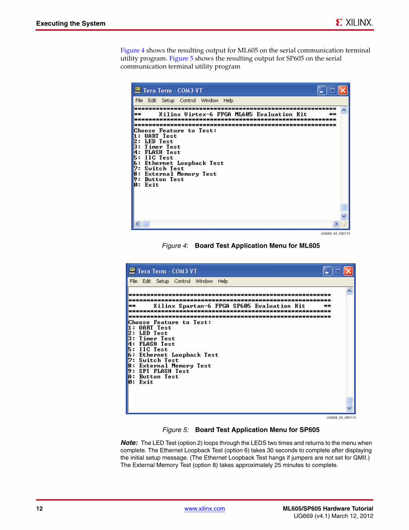
Figure 4 shows the resulting output for ML605 on the serial communication terminal utility program. Figure 5 shows the resulting output for SP605 on the serial communication terminal utility program
Note: The LED Test (option 2) loops through the LEDS two times and returns to the menu when complete. The Ethernet Loopback Test (option 6) takes 30 seconds to complete after displaying the initial setup message. (The Ethernet Loopback Test hangs if jumpers are not set for GMII.) The External Memory Test (option 8) takes approximately 25 minutes to complete.
X-Ref Target - Figure 4
Figure 4: Board Test Application Menu for ML605
X-Ref Target - Figure 5
Figure 5: Board Test Application Menu for SP605
UG669_04_092110
UG669_05_092110
ML605/SP605 Hardware Tutorial www.xilinx.com 13UG669 (v4.1) March 12, 2012
Executing the System
9. Execute the chosen tests and then select 0 to exit. Details about the test options can be found in the UG670, AXI Interface Based ML605/SP605 MicroBlaze Processor Subsystem Software Tutorial [Ref 7].
10. When software execution is completed, enter these commands:
XMD% stop
XMD% rst
XMD% exit
14 www.xilinx.com ML605/SP605 Hardware TutorialUG669 (v4.1) March 12, 2012
System Design Flow
System Design FlowThe design flow for creating the base MicroBlaze Processor Subsystem and modifying the system to include the benchmarking cores includes these steps:
1. Hardware Platform Creation
2. Exporting the Base Hardware Platform to SDK, page 22
3. Customizing the Embedded Hardware Platform, page 24
4. Implementing and Downloading the Design, page 35
5. Testing the Design, page 35
Allocate approximately 90 minutes for parts 1 and 2. The bulk of this tutorial is within parts 3 through 5 which takes approximately two hours to complete.
Note: All time estimates are subject to host computer system speed and can vary depending on how much time is spent executing the software applications.
Hardware Platform Creation
Opening the Project
1. Start ISE.
• On a Windows XP host, select Start → All Programs → Xilinx ISE Design Suite 13.x → ISE Design Tools → Project Navigator.
• On a Linux host, enter ise at a command prompt.
2. If necessary, close out the previous project by selecting File → Close Project.
3. In Project Commands, select Open Project...
4. Browse to
ML605_Embedded_Kit/Tutorial_Sandbox/HW
or
SP605_Embedded_Kit/Tutorial_Sandbox/HW
and select ise_proj.xise. Click Open.
5. Under Hierarchy, expand ise_top - STRUCTURE and double click on system_i - system (system.xmp). This invokes XPS for the XPS subsystem.
ML605/SP605 Hardware Tutorial www.xilinx.com 15UG669 (v4.1) March 12, 2012
System Design Flow
Examining the System
The System Assembly View (SAV) of the design provides visibility of the MicroBlaze Processor Subsystem bus interfaces, port connections, and address map.
Note: Refer to UG683, EDK Concepts, Tools, and Techniques for additional details or instructions for any of the steps outlined in this section of the tutorial. [Ref 1]
Bus Interfaces
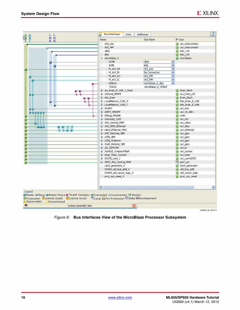
1. To examine the bus structure of the MicroBlaze Processor Subsystem, select the System Assembly View tab and then select the Bus Interfaces tab along the top edge of the workspace as shown in Figure 6.
For MicroBlaze masters (Instruction Cache (IC), Data Cache (DC), and Data Port (DP)), both AXI_MM and AXI_Lite interconnects are used. Two Local Memory Buses (LMB) are used by MicroBlaze to interface to the local BRAM memory for the processor. These bus interfaces on MicroBlaze are seen by clicking the + to the left of the microblaze_0 component. (See Figure 6).
16 www.xilinx.com ML605/SP605 Hardware TutorialUG669 (v4.1) March 12, 2012
System Design Flow
X-Ref Target - Figure 6
Figure 6: Bus Interfaces View of the MicroBlaze Processor Subsystem
UG669_06_061011
ML605/SP605 Hardware Tutorial www.xilinx.com 17UG669 (v4.1) March 12, 2012
System Design Flow
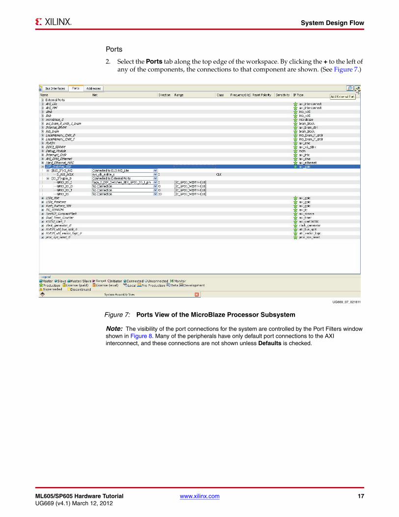
Ports
2. Select the Ports tab along the top edge of the workspace. By clicking the + to the left of any of the components, the connections to that component are shown. (See Figure 7.)
Note: The visibility of the port connections for the system are controlled by the Port Filters window shown in Figure 8. Many of the peripherals have only default port connections to the AXI interconnect, and these connections are not shown unless Defaults is checked.
X-Ref Target - Figure 7
Figure 7: Ports View of the MicroBlaze Processor Subsystem
UG669_07_021611
18 www.xilinx.com ML605/SP605 Hardware TutorialUG669 (v4.1) March 12, 2012
System Design Flow
Addresses
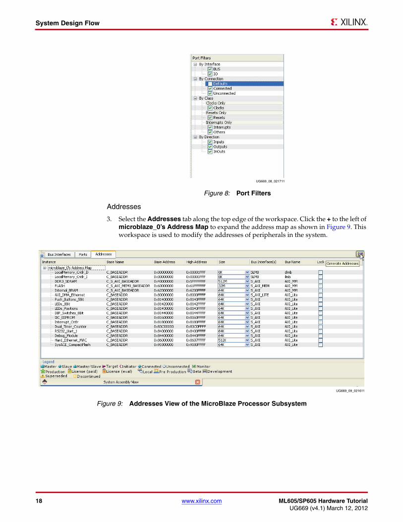
3. Select the Addresses tab along the top edge of the workspace. Click the + to the left of microblaze_0’s Address Map to expand the address map as shown in Figure 9. This workspace is used to modify the addresses of peripherals in the system.
X-Ref Target - Figure 8
Figure 8: Port Filters
UG669_08_021711
X-Ref Target - Figure 9
Figure 9: Addresses View of the MicroBlaze Processor Subsystem
UG669_09_021611
ML605/SP605 Hardware Tutorial www.xilinx.com 19UG669 (v4.1) March 12, 2012
System Design Flow
IP Core Configurations
The IP cores within the system are configured to the required functionality for this embedded system. The configurations of the IP cores are described in the System Configuration section of DS668, AXI Interface Based ML605 Embedded Kit MicroBlaze Processor Subsystem Data Sheet [Ref 3] and DS667, AXI Interface Based SP605 Embedded Kit MicroBlaze Processor Subsystem Data Sheet [Ref 5].
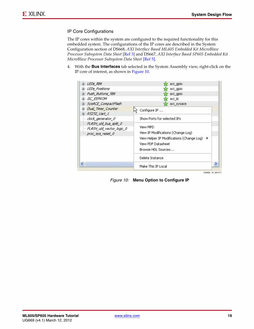
4. With the Bus Interfaces tab selected in the System Assembly view, right-click on the IP core of interest, as shown in Figure 10.
X-Ref Target - Figure 10
Figure 10: Menu Option to Configure IP
UG669_10_061011
20 www.xilinx.com ML605/SP605 Hardware TutorialUG669 (v4.1) March 12, 2012
System Design Flow
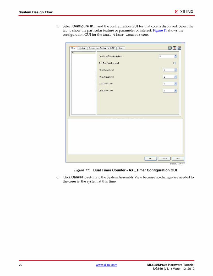
5. Select Configure IP... and the configuration GUI for that core is displayed. Select the tab to show the particular feature or parameter of interest. Figure 11 shows the configuration GUI for the Dual_Timer_Counter core.
6. Click Cancel to return to the System Assembly View because no changes are needed to the cores in the system at this time.
X-Ref Target - Figure 11
Figure 11: Dual Timer Counter - AXI_Timer Configuration GUI
UG669_11_061011
ML605/SP605 Hardware Tutorial www.xilinx.com 21UG669 (v4.1) March 12, 2012
System Design Flow
Generating the Hardware Platform
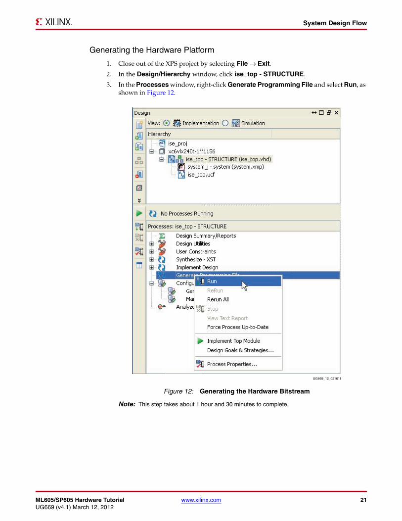
1. Close out of the XPS project by selecting File → Exit.
2. In the Design/Hierarchy window, click ise_top - STRUCTURE.
3. In the Processes window, right-click Generate Programming File and select Run, as shown in Figure 12.
Note: This step takes about 1 hour and 30 minutes to complete.
X-Ref Target - Figure 12
Figure 12: Generating the Hardware Bitstream
UG669_12_021611
22 www.xilinx.com ML605/SP605 Hardware TutorialUG669 (v4.1) March 12, 2012
System Design Flow
Exporting the Base Hardware Platform to SDK Because the base hardware platform is used with the Software Development Kit (SDK) described in UG670, AXI Interface Based ML605/SP605 MicroBlaze Processor Subsystem Software Tutorial, [Ref 7] information about the hardware platform must be provided to the SDK to allow development of software platforms and applications. To export this base hardware platform to SDK:
1. When bitstream generation is complete:
a. Under Hierarchy, click on system_i - system (system.xmp).
b. Under Processes, right click Export Hardware Design to SDK with Bitstream and select Run.
The hardware description files are stored in the following location:
• For ML605:
ML605_Embedded_Kit/Tutorial_Sandbox/HW/Microblaze_ProcessorSubSystem/SDK/SDK_Export
• For SP605:
SP605_Embedded_Kit/Tutorial_Sandbox/HW/Microblaze_ProcessorSubSystem/SDK/SDK_Export
SDK is extensively run while executing the AXI Interface Based ML605/SP605 MicroBlaze Processor Subsystem Software Tutorial.
2. Copy the SDK_Export directory into the SW area of the Tutorial sandbox for use with UG670, AXI Interface Based ML605/SP605 MicroBlaze Processor Subsystem Software Tutorial [Ref 7]. The directory that already exists can be overwritten.
• For ML605:
Copy
ML605_Embedded_Kit\Tutorial_Sandbox\HW\MicroBlaze_ProcessorSubsystem\SDK\SDK_Export
to
ML605_Embedded_Kit\Tutorial_Sandbox\SW\standalone
• For SP605:
Copy
SP605_Embedded_Kit\Tutorial_Sandbox\HW\MicroBlaze_ProcessorSubsystem\SDK\SDK_Export
to
SP605_Embedded_Kit\Tutorial_Sandbox\SW\standalone
ML605/SP605 Hardware Tutorial www.xilinx.com 23UG669 (v4.1) March 12, 2012
System Design Flow
Downloading and Verifying the Design
1. Verify that the two USB cables are properly connected between the host computer and the USB -JTAG and USB-UART connections on the ML605 or SP605 board.
2. In the ISE project, under Hierarchy, expand ise_top - STRUCTURE and double click system_i - system (system.xmp). This invokes XPS for the XPS subsystem.
3. In XPS, invoke a Xilinx shell by selecting Project > Launch Xilinx Bash Shell.
4. In the shell, enter xmd and press Enter to invoke XMD.
5. To download the bitstream, enter this command at the XMD command prompt:
XMD% fpga -f implementation/download.bit
After the FPGA is programmed, the software can be downloaded and executed.
6. Open and configure a serial communications terminal utility program on the host computer with these settings:
• Baud Rate: 9600
• Data: 8 bit
• Parity: None
• Stop: 1 bit
• Flow Control: None
(See Figure 3.)
7. Connect to the processor by entering the connect mb mdm command.
8. To download and execute the test software application, enter these commands at the XMD command prompt:
• For ML605:
XMD% dow ../../../ML605_System/ready_for_download/board_test_app.elf
XMD% con
• For SP605:
XMD% dow ../../../SP605_System/ready_for_download/board_test_app.elf
XMD% con
The UART output should be displayed and look similar to Figure 4 or Figure 5.
9. Execute the chosen tests and then select 0 to exit. Refer to UG670, AXI Interface Based ML605/SP605 MicroBlaze Processor Subsystem Software Tutorial for details about these test options [Ref 7].
10. When the software execution is completed, enter these commands:
XMD% stop
XMD% rst
XMD% exit
11. Exit out of the bash Shell by entering exit.
At this point in the tutorial, the ML605 or SP605 MicroBlaze Processor Subsystem is successfully built, verified, and exported for use with the Xilinx Software Development Kit (SDK). If no modifications to the hardware subsystem are required, proceed with the tutorial presented in UG670, AXI Interface Based ML605/SP605 MicroBlaze Processor Subsystem Software Tutorial [Ref 7].
24 www.xilinx.com ML605/SP605 Hardware TutorialUG669 (v4.1) March 12, 2012
System Design Flow
Customizing the Embedded Hardware PlatformIn this section of the tutorial, the MicroBlaze Processor Subsystem is modified to include an additional AXI_CDMA and associated benchmarking cores to the system. The AXI_CDMA core contains two master interfaces (SG engine and data) and a slave interface. The AXI_CDMA in this tutorial is setup for simple DMA (no SG engine).
The Perf_AXI core starts counting with the first read of the AXI_CDMA master and stops with the interrupt of the AXI_CDMA core. The core also contains a slave AXI interface for control/status and counter value registers.
After building the hardware, the benchmarking demonstration application uses a Web server to display the benchmarking data.
Every data point consists of a data transfer of 1,152,000 bytes by means of the AXI_CDMA (simple DMA operation which copies data from one area of the main memory to another area of main memory). The Perf_AXI core (which is added to the system) monitors this transaction through monitoring signals on the AXI interface master and counts from the start of the transfer (first read address accepted) to when the core interrupts (transfer is complete). A block diagram of this system is as shown in Figure 13.
For the ML605 board the AXI_CDMA is running at 151.515151 MHz with a 32-bit interface. The theoretical throughput on one channel is 606.060606 MB/s. The aggregate throughput is 1,212 MB/s.
For the SP605 board the AXI_CDMA is running at 100 MHz with a 32-bit interface. The theoretical throughput on one channel is 400 MB/s. The aggregate throughput is 800 MB/s.
Because both reads and writes are occurring during the AXI_CDMA transfer, the number represented in the Benchmark Graph is doubled for the total throughput or aggregate throughput (both read and write).
The steps to customize the MicroBlaze Processor Subsystem include:
1. Adding IP from the Xilinx IP Catalog, page 26
2. Connecting the Bus Interfaces, page 29
3. Connecting Ports, page 33
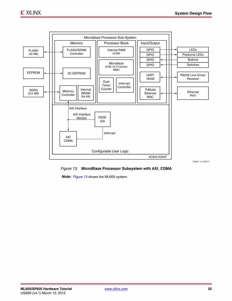
ML605/SP605 Hardware Tutorial www.xilinx.com 25UG669 (v4.1) March 12, 2012
System Design Flow
Note: Figure 13 shows the ML605 system.
X-Ref Target - Figure 13
Figure 13: MicroBlaze Processor Subsystem with AXI_CDMA
FLASH(32 MB)
FLASH/SRAMController
Internal RAM(8 KB)
Microblaze8 KB I & D Caches
MMU
DualTimer/
Counter
InterruptController
AXI Interface
AXI InterfaceMonitor
Interrupt
GPIO
GPIO
GPIO
UART16550
RS232 Line Driver/Receiver
EthernetPHY
TriModeEthernet
MAC
LEDs
Positional LEDs
Buttons
GPIO Swtiches
Memory Processor Block Input/Output
Microblaze Processor Sub-System
Configurable User Logic
XC6VLX240T
IIC EEPROM
MemoryController
AXICDMA
InternalBRAM(64 KB)
PERFAXI
EEPROM
DDR3(512 MB)
UG669_14_092910
26 www.xilinx.com ML605/SP605 Hardware TutorialUG669 (v4.1) March 12, 2012
System Design Flow
Adding IP from the Xilinx IP Catalog
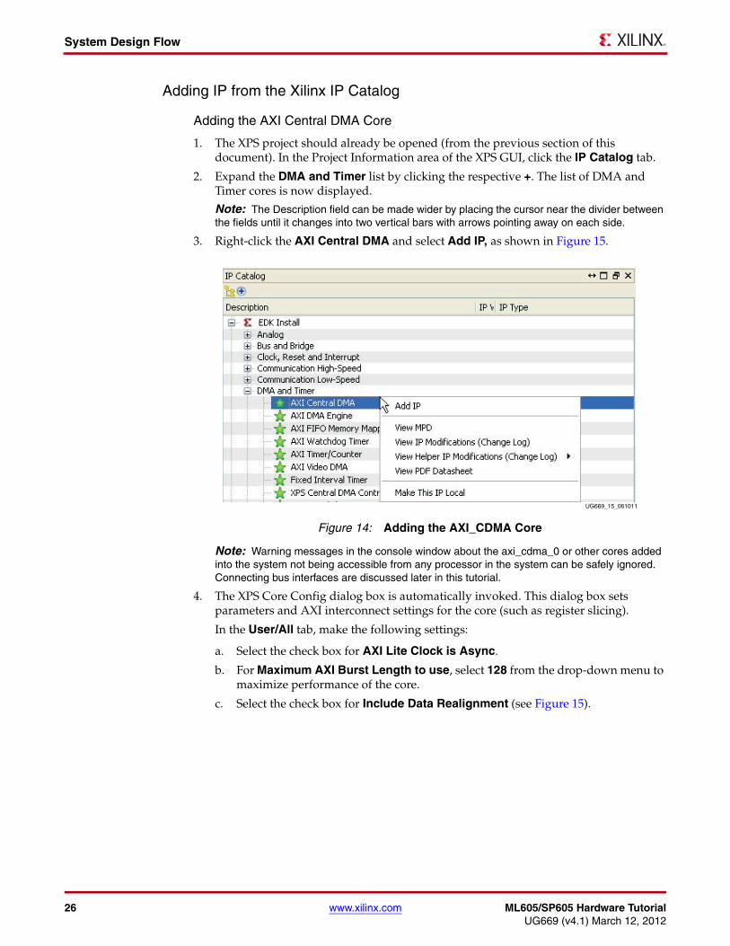
Adding the AXI Central DMA Core
1. The XPS project should already be opened (from the previous section of this document). In the Project Information area of the XPS GUI, click the IP Catalog tab.
2. Expand the DMA and Timer list by clicking the respective +. The list of DMA and Timer cores is now displayed.
Note: The Description field can be made wider by placing the cursor near the divider between the fields until it changes into two vertical bars with arrows pointing away on each side.
3. Right-click the AXI Central DMA and select Add IP, as shown in Figure 15.
Note: Warning messages in the console window about the axi_cdma_0 or other cores added into the system not being accessible from any processor in the system can be safely ignored. Connecting bus interfaces are discussed later in this tutorial.
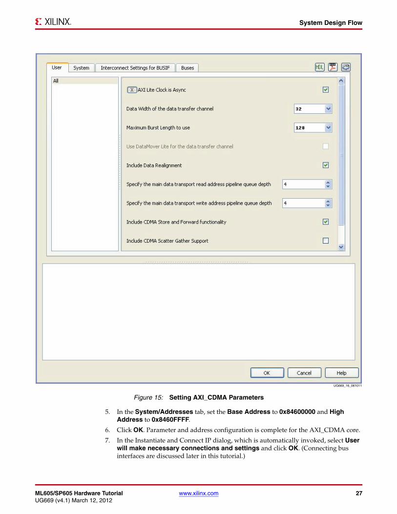
4. The XPS Core Config dialog box is automatically invoked. This dialog box sets parameters and AXI interconnect settings for the core (such as register slicing).
In the User/All tab, make the following settings:
a. Select the check box for AXI Lite Clock is Async.
b. For Maximum AXI Burst Length to use, select 128 from the drop-down menu to maximize performance of the core.
c. Select the check box for Include Data Realignment (see Figure 15).
X-Ref Target - Figure 14
Figure 14: Adding the AXI_CDMA Core
UG669_15_061011
ML605/SP605 Hardware Tutorial www.xilinx.com 27UG669 (v4.1) March 12, 2012
System Design Flow
5. In the System/Addresses tab, set the Base Address to 0x84600000 and High Address to 0x8460FFFF.
6. Click OK. Parameter and address configuration is complete for the AXI_CDMA core.
7. In the Instantiate and Connect IP dialog, which is automatically invoked, select User will make necessary connections and settings and click OK. (Connecting bus interfaces are discussed later in this tutorial.)
X-Ref Target - Figure 15
Figure 15: Setting AXI_CDMA Parameters
UG669_16_061011
28 www.xilinx.com ML605/SP605 Hardware TutorialUG669 (v4.1) March 12, 2012
System Design Flow
Adding the Perf_AXI core
1. In the Project Information Area of the XPS GUI, click the IP Catalog tab.
2. Expand the Project Local PCores by clicking the respective +. Expand the USER by clicking the respective +. Right-click on PERF_AXI and select Add IP.
3. Inside the XPS Core Config dialog box, set C_BASEADDR to 0x90000000 and C_HIGHADDR to 0x9000FFFF.
The C_MSTID and C_MSTID_WIDTH are dependent on the connection of the AXI_CDMA master to the AXI interconnect. The C_MSTID_WIDTH is the size of the signal for both ARVALID and ARREADY signals which depend on the number of masters connected to the interconnect. Each master uses 1 bit of these signals. The C_MSTID identifies the master's bit for the ARVALID and ARREAD signals.
• For ML605:
Set C_MSTID to 5 and C_MSTID_WIDTH to 6.
• For SP605:
Set C_MSTID to 2 and C_MSTID_WIDTH to 3.
4. Click OK.
5. In the Instantiate and Connect IP dialog box, select User will make necessary connections and settings and click OK. (Connecting bus interfaces are discussed later in this tutorial.)
ML605/SP605 Hardware Tutorial www.xilinx.com 29UG669 (v4.1) March 12, 2012
System Design Flow
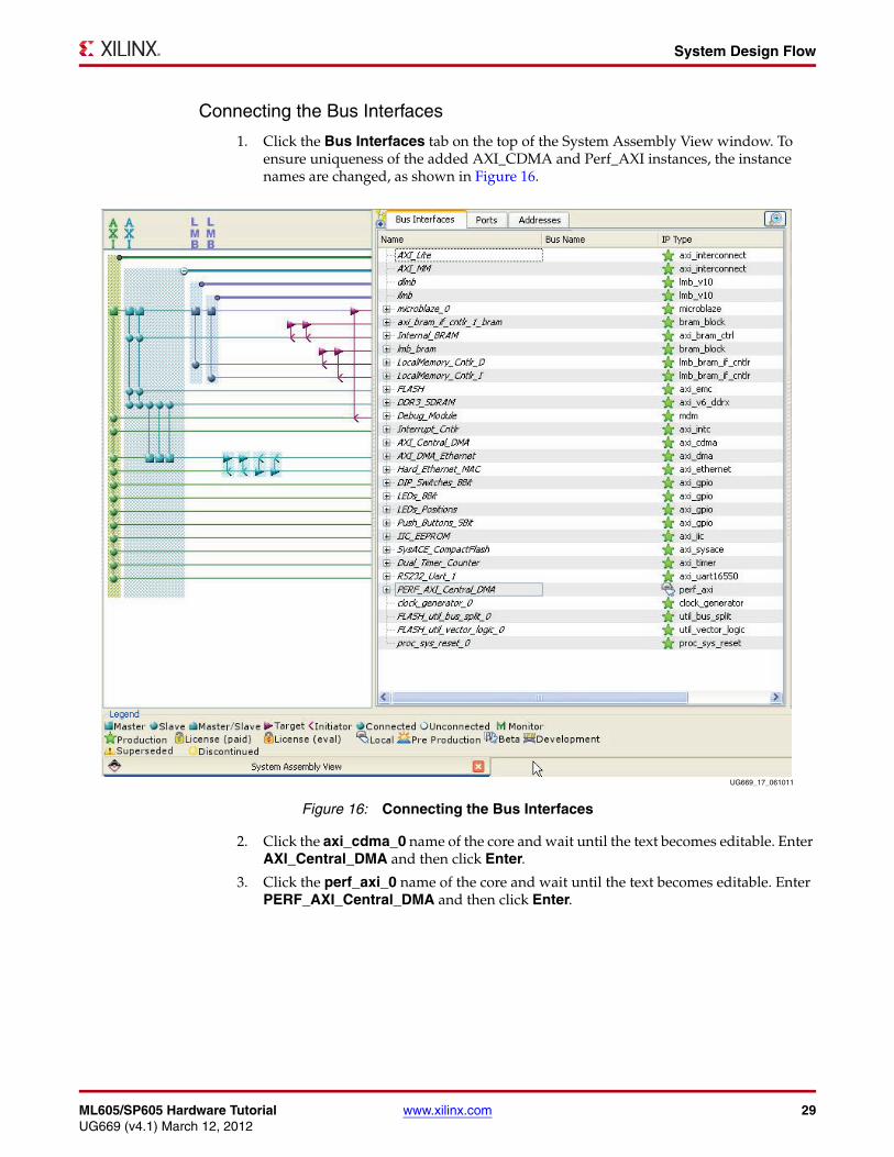
Connecting the Bus Interfaces
1. Click the Bus Interfaces tab on the top of the System Assembly View window. To ensure uniqueness of the added AXI_CDMA and Perf_AXI instances, the instance names are changed, as shown in Figure 16.
2. Click the axi_cdma_0 name of the core and wait until the text becomes editable. Enter AXI_Central_DMA and then click Enter.
3. Click the perf_axi_0 name of the core and wait until the text becomes editable. Enter PERF_AXI_Central_DMA and then click Enter.
X-Ref Target - Figure 16
Figure 16: Connecting the Bus Interfaces
UG669_17_061011
30 www.xilinx.com ML605/SP605 Hardware TutorialUG669 (v4.1) March 12, 2012
System Design Flow
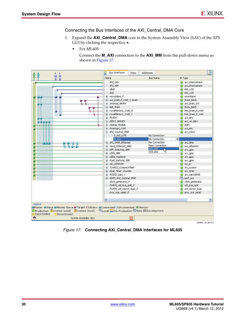
Connecting the Bus Interfaces of the AXI_Central_DMA Core
1. Expand the AXI_Central_DMA core in the System Assembly View (SAV) of the XPS GUI by clicking the respective +.
• For ML605:
Connect the M_AXI connection to the AXI_MM from the pull-down menu as shown in Figure 17.
X-Ref Target - Figure 17
Figure 17: Connecting AXI_Central_DMA Interfaces for ML605
UG669_18_061011
ML605/SP605 Hardware Tutorial www.xilinx.com 31UG669 (v4.1) March 12, 2012
System Design Flow
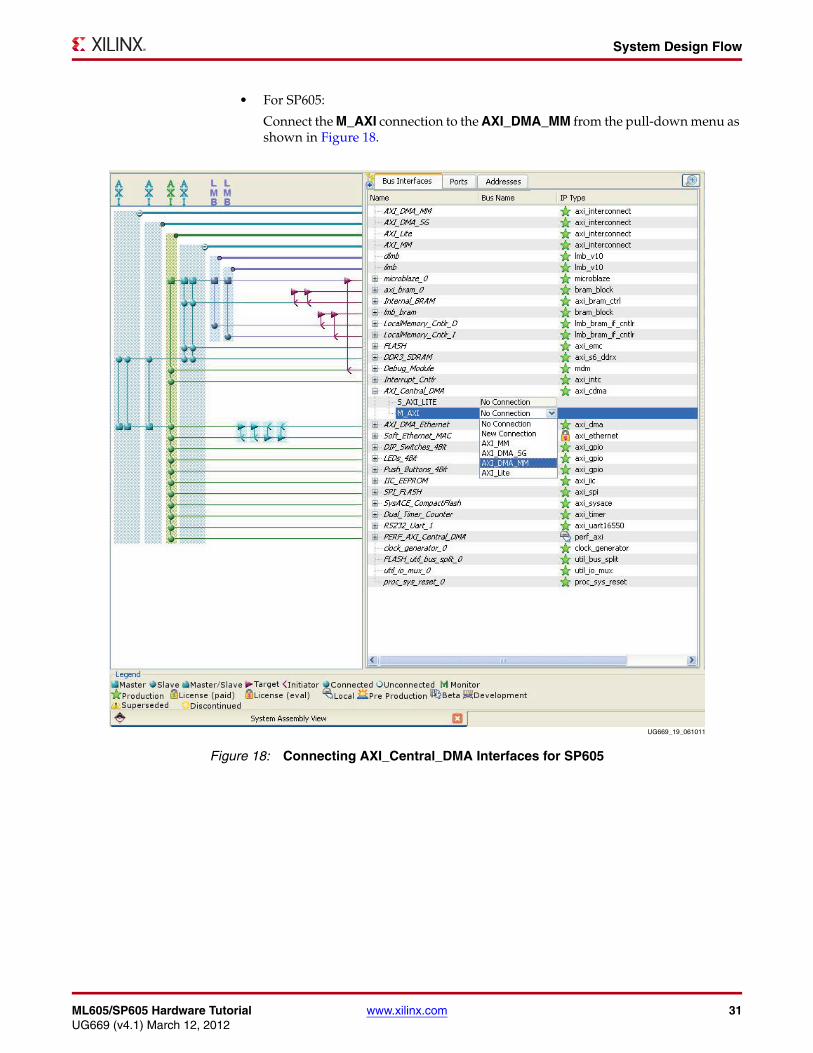
• For SP605:
Connect the M_AXI connection to the AXI_DMA_MM from the pull-down menu as shown in Figure 18.
X-Ref Target - Figure 18
Figure 18: Connecting AXI_Central_DMA Interfaces for SP605
UG669_19_061011
32 www.xilinx.com ML605/SP605 Hardware TutorialUG669 (v4.1) March 12, 2012
System Design Flow
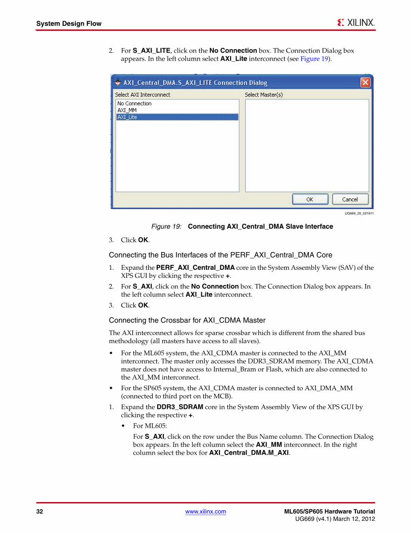
2. For S_AXI_LITE, click on the No Connection box. The Connection Dialog box appears. In the left column select AXI_Lite interconnect (see Figure 19).
3. Click OK.
Connecting the Bus Interfaces of the PERF_AXI_Central_DMA Core
1. Expand the PERF_AXI_Central_DMA core in the System Assembly View (SAV) of the XPS GUI by clicking the respective +.
2. For S_AXI, click on the No Connection box. The Connection Dialog box appears. In the left column select AXI_Lite interconnect.
3. Click OK.
Connecting the Crossbar for AXI_CDMA Master
The AXI interconnect allows for sparse crossbar which is different from the shared bus methodology (all masters have access to all slaves).
• For the ML605 system, the AXI_CDMA master is connected to the AXI_MM interconnect. The master only accesses the DDR3_SDRAM memory. The AXI_CDMA master does not have access to Internal_Bram or Flash, which are also connected to the AXI_MM interconnect.
• For the SP605 system, the AXI_CDMA master is connected to AXI_DMA_MM (connected to third port on the MCB).
1. Expand the DDR3_SDRAM core in the System Assembly View of the XPS GUI by clicking the respective +.
• For ML605:
For S_AXI, click on the row under the Bus Name column. The Connection Dialog box appears. In the left column select the AXI_MM interconnect. In the right column select the box for AXI_Central_DMA.M_AXI.
X-Ref Target - Figure 19
Figure 19: Connecting AXI_Central_DMA Slave Interface
UG669_20_021611
ML605/SP605 Hardware Tutorial www.xilinx.com 33UG669 (v4.1) March 12, 2012
System Design Flow
• For SP605:
For S2_AXI, click on the row under the Bus Name column. The Connection Dialog box appears. In the left column select the AXI_DMA_MM interconnect. In the right column select the box for AXI_Central_DMA.M_AXI.
3. Click OK.
Connecting Ports
The section covers connecting clock pins, interrupts, and signals for the PERF_AXI_Central_DMA. In the Port Filters, ensure that Defaults is selected.
1. Click on the Ports tab at the top of the System Assembly View window.
2. Expand the Interrupt_Cntlr core in the System Assembly View of the XPS GUI by clicking the respective +.
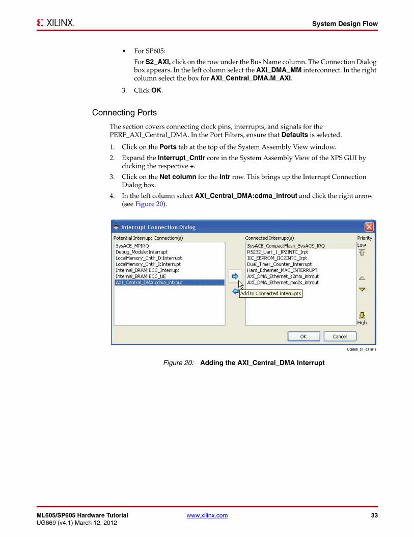
3. Click on the Net column for the Intr row. This brings up the Interrupt Connection Dialog box.
4. In the left column select AXI_Central_DMA:cdma_introut and click the right arrow (see Figure 20).
X-Ref Target - Figure 20
Figure 20: Adding the AXI_Central_DMA Interrupt
UG669_21_021611
34 www.xilinx.com ML605/SP605 Hardware TutorialUG669 (v4.1) March 12, 2012
System Design Flow
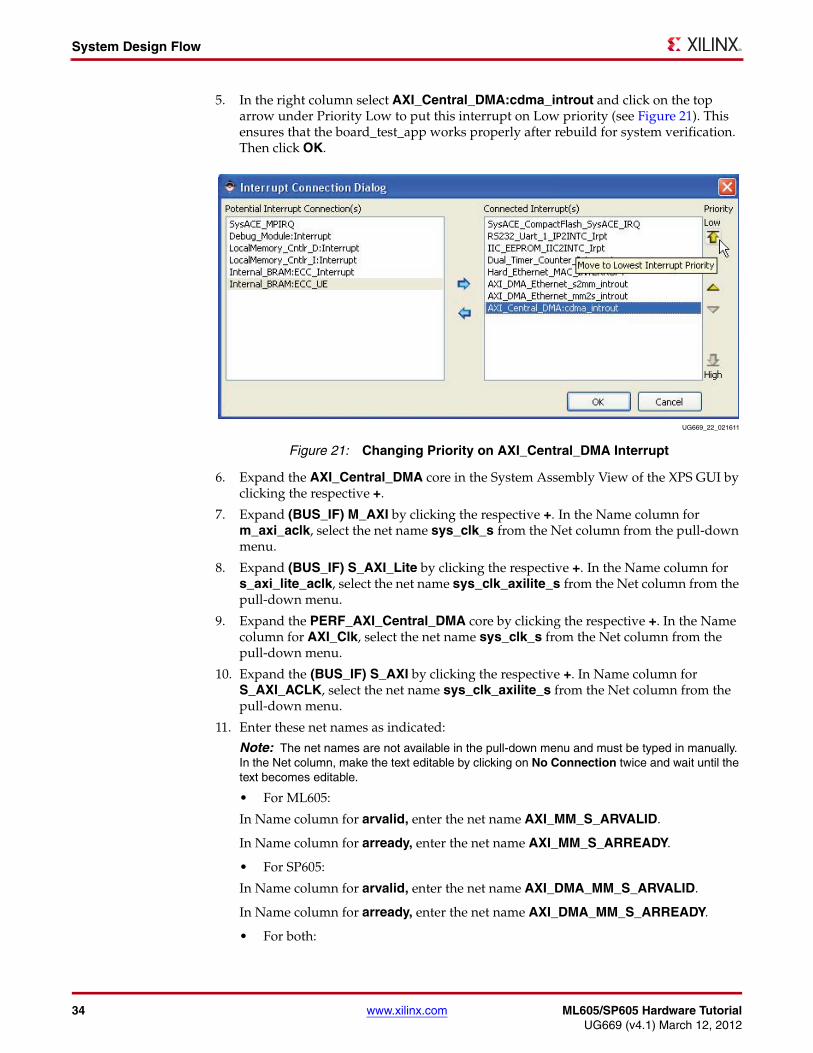
5. In the right column select AXI_Central_DMA:cdma_introut and click on the top arrow under Priority Low to put this interrupt on Low priority (see Figure 21). This ensures that the board_test_app works properly after rebuild for system verification. Then click OK.
6. Expand the AXI_Central_DMA core in the System Assembly View of the XPS GUI by clicking the respective +.
7. Expand (BUS_IF) M_AXI by clicking the respective +. In the Name column for m_axi_aclk, select the net name sys_clk_s from the Net column from the pull-down menu.
8. Expand (BUS_IF) S_AXI_Lite by clicking the respective +. In the Name column for s_axi_lite_aclk, select the net name sys_clk_axilite_s from the Net column from the pull-down menu.
9. Expand the PERF_AXI_Central_DMA core by clicking the respective +. In the Name column for AXI_Clk, select the net name sys_clk_s from the Net column from the pull-down menu.
10. Expand the (BUS_IF) S_AXI by clicking the respective +. In Name column for S_AXI_ACLK, select the net name sys_clk_axilite_s from the Net column from the pull-down menu.
11. Enter these net names as indicated:
Note: The net names are not available in the pull-down menu and must be typed in manually. In the Net column, make the text editable by clicking on No Connection twice and wait until the text becomes editable.
• For ML605:
In Name column for arvalid, enter the net name AXI_MM_S_ARVALID.
In Name column for arready, enter the net name AXI_MM_S_ARREADY.
• For SP605:
In Name column for arvalid, enter the net name AXI_DMA_MM_S_ARVALID.
In Name column for arready, enter the net name AXI_DMA_MM_S_ARREADY.
• For both:
X-Ref Target - Figure 21
Figure 21: Changing Priority on AXI_Central_DMA Interrupt
UG669_22_021611

ML605/SP605 Hardware Tutorial www.xilinx.com 35UG669 (v4.1) March 12, 2012
System Design Flow
In Name column for Intr, enter the net name AXI_Central_DMA_cdma_introut.
At this point in the tutorial, additional IP from the Xilinx IP Catalog has successfully been added to the ML605 or SP605 MicroBlaze Processor Subsystem.
Implementing and Downloading the DesignThe design is ready to be synthesized, mapped, placed, and routed in the chosen FPGA architecture.
1. Close out of the XPS project by selecting File → Exit.
2. In the Design/Hierarchy window, click ise_top - STRUCTURE.
3. In the Processes window, right-click Generate Programming File and select Run, as shown in Figure 12.
Note: Depending on the host system running ISE and XPS, this step could take between 30 minutes and one hour to complete.
4. Verify that a USB cable is properly connected between the host computer and the USB-JTAG connection on the ML605 or SP605 board.
5. Verify that the board is powered on.
6. In the ISE project, under Hierarchy, expand ise_top - STRUCTURE and double click system_i - system (system.xmp). This invokes XPS for the XPS subsystem.
7. In XPS, invoke a Xilinx shell by selecting Project > Launch Xilinx Shell.
8. In the shell, enter xmd and press Enter to invoke XMD.
9. To download the bitstream, enter this command at the XMD command prompt:
XMD% fpga -f implementation/download.bit
After the FPGA is programmed, the software can be downloaded and executed.
Testing the Design1. Verify that a USB cable is properly connected between the host computer and the
USB-UART connection on the ML605 board or SP605 board.
2. Open and configure a serial communications terminal utility program on the host computer with these settings:
• Baud Rate: 9600
• Data: 8 bit
• Parity: None
• Stop: 1 bit
• Flow Control: None
(See Figure 3, page 9.)
3. Connect the ML605 or SP605 board to an Ethernet port on a computer via an Ethernet Cable.
4. Assign the IP address of the computer to 192.168.1.100.
Note: The demonstration uses a hard-coded MAC address and a fixed IP address of 192.168.1.10 and does not connect to the regular LAN network using DHCP. Do not connect more than one board to the same network segment.
5. Connect to the processor by entering the command connect mb mdm.
36 www.xilinx.com ML605/SP605 Hardware TutorialUG669 (v4.1) March 12, 2012
System Design Flow
6. To download and execute the test software application, enter the following command at the XMD command prompt:
• For ML605:
XMD% dow ../../../ML605_System/ready_for_download/board_test_app.elf
XMD% con
• For SP605:
XMD% dow ../../../SP605_System/ready_for_download/board_test_app.elf
XMD% con
Note: The initial display on the terminal window should be the same as shown in Figure 4, page 12 or Figure 5, page 12.
7. When all of the desired tests have been run and software execution has completed, enter:
XMD% stop
XMD% rst
8. To download and execute the Web Server to test the design, enter:
XMD% dow ../../../Benchmark_Demo/ready_for_download/BenchmarkDemo.elf
XMD% con
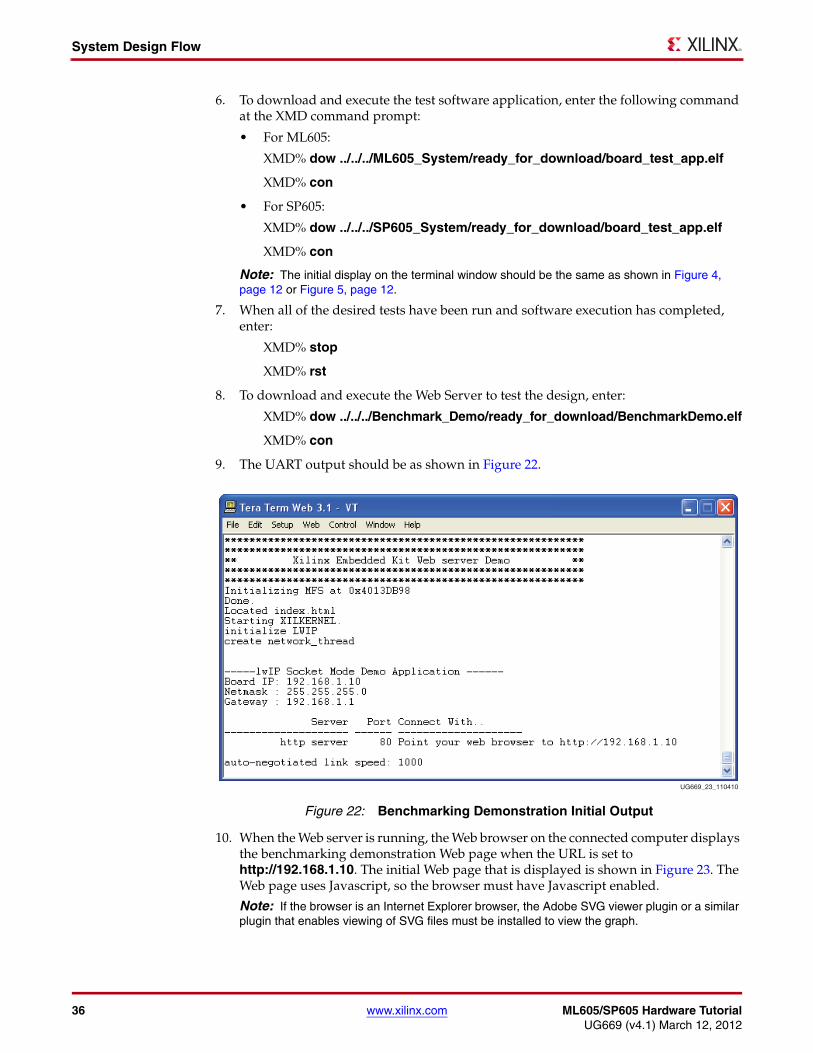
9. The UART output should be as shown in Figure 22.
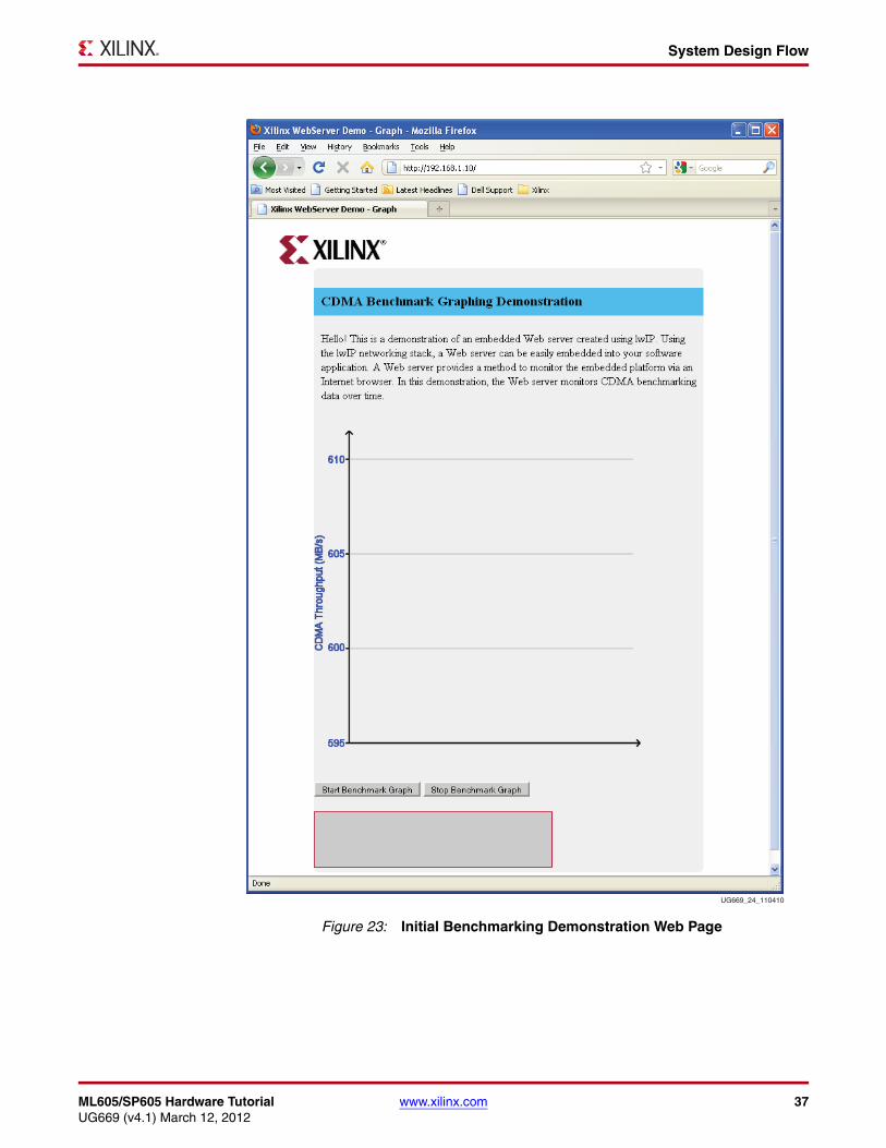
10. When the Web server is running, the Web browser on the connected computer displays the benchmarking demonstration Web page when the URL is set tohttp://192.168.1.10. The initial Web page that is displayed is shown in Figure 23. The Web page uses Javascript, so the browser must have Javascript enabled.
Note: If the browser is an Internet Explorer browser, the Adobe SVG viewer plugin or a similar plugin that enables viewing of SVG files must be installed to view the graph.
X-Ref Target - Figure 22
Figure 22: Benchmarking Demonstration Initial Output
UG669_23_110410
ML605/SP605 Hardware Tutorial www.xilinx.com 37UG669 (v4.1) March 12, 2012
System Design Flow
X-Ref Target - Figure 23
Figure 23: Initial Benchmarking Demonstration Web Page
UG669_24_110410
38 www.xilinx.com ML605/SP605 Hardware TutorialUG669 (v4.1) March 12, 2012
System Design Flow
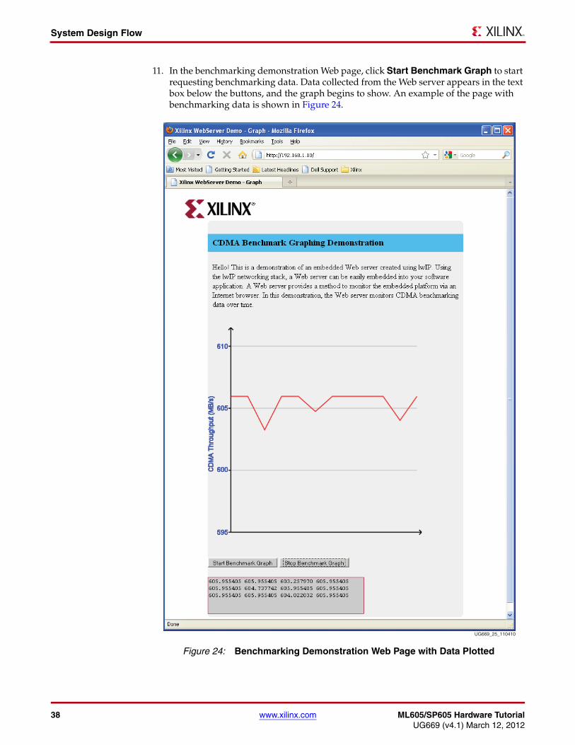
11. In the benchmarking demonstration Web page, click Start Benchmark Graph to start requesting benchmarking data. Data collected from the Web server appears in the text box below the buttons, and the graph begins to show. An example of the page with benchmarking data is shown in Figure 24.
X-Ref Target - Figure 24
Figure 24: Benchmarking Demonstration Web Page with Data Plotted
UG669_25_110410
ML605/SP605 Hardware Tutorial www.xilinx.com 39UG669 (v4.1) March 12, 2012
System Design Flow
The Web browser receives one CDMA benchmark result at a time. Javascript is used to convert the benchmark result into coordinates and update the graph. The graph updates every time a new data point is received. The graph holds a maximum of 12 data points at a time. After the maximum has been reached, the oldest data point is dropped and the newest data point is added.
In the benchmarking demonstration Web page, click Stop Benchmark Graph to stop requesting benchmarking data. After this button is clicked, any pending requests are completed and no additional data is requested.
12. When finished, in the XMD window enter:
XMD% stop
XMD% rst
XMD% exit
Adding the AXI_CDMA with benchmarking cores to analyze performance from the base MicroBlaze Processor Subsystem is completed.
40 www.xilinx.com ML605/SP605 Hardware TutorialUG669 (v4.1) March 12, 2012
Summary
SummaryTasks accomplished in this tutorial:
• Loading and executing a design from a pre-built bitstream and ELF
• Rebuilding a design
• Adding IP from the Xilinx IP catalog to an embedded system
• Adding user IP to an embedded system
Next Steps
References1. UG683, EDK Concepts, Tools, and Techniques
2. UG668, Getting Started with the Virtex-6 FPGA ML605 Embedded Kit
3. DS668, AXI Interface Based ML605 Embedded Kit MicroBlaze Processor Subsystem Data Sheet
4. UG667, Getting Started with the Spartan-6 FPGA SP605 Embedded Kit
5. DS667, AXI Interface Based SP605 Embedded Kit MicroBlaze Processor Subsystem Data Sheet
6. UG111, Embedded System Tools Reference Manual EDK 13.4, Chapter 10, Xilinx Microprocessor Debugger (XMD)
7. UG670, AXI Interface Based ML605/SP605 MicroBlaze Processor Subsystem Software Tutorial
8. UG029, ChipScope Pro 13.4 Software and Cores User Guide
9. UG534, ML605 Hardware User Guide
10. UG526, SP605 Hardware User Guide
11. UG081, MicroBlaze Processor Reference Guide EDK 13.4
Note: UG667 and, DS667, are provided in the SP605_Embedded_Kit\Documentation directory. UG668 and, DS668, are provided in the ML605_Embedded_Kit\Documentation directory
Next Step Refer To
Develop the Software Platform UG670, AXI Interface Based ML605/SP605 MicroBlaze Processor Subsystem Software Tutorial [Ref 7]
Advanced Debugging UG029, ChipScope Pro Software and Cores User Guide [Ref 8] and UG111, Embedded System Tools Reference Manual EDK 12.3, Chapter 9 [Ref 6]
Simulate the Embedded System UG683, EDK Concepts, Tools, and Techniques [Ref 1]


![Xilinx UGxxx [Guide Title] · 2019-12-14 · Debugging with ChipScope 7 UG677 (v14.2) July 25, 2012 Getting Started Table 1: Pinout Information for the SP601, SP605, ML605, or KC705](https://img.dokumen.tips/doc/110x75/5f834a9ecfbc390a9a0cd8b8/xilinx-ugxxx-guide-title-2019-12-14-debugging-with-chipscope-7-ug677-v142.jpg)