Embed Size (px)
Citation preview
Dynamic Article LinksC<Journal ofMaterials Chemistry
Cite this: J. Mater. Chem., 2012, 22, 20786
www.rsc.org/materials PAPER
Publ
ishe
d on
03
Sept
embe
r 20
12. D
ownl
oade
d by
Uni
vers
ity o
f So
uthe
rn C
alif
orni
a on
05/
04/2
014
14:4
1:48
. View Article Online / Journal Homepage / Table of Contents for this issue
Auto-catalysed crosslinking for next-generation OLED-design†
Daniel Volz,c Thomas Baumann,*a Harald Fl€ugge,a Mathias Mydlak,a Tobias Grab,a Michael B€achle,a
Christopher Barner-Kowollik*b and Stefan Br€ase*c
Received 23rd May 2012, Accepted 14th August 2012
DOI: 10.1039/c2jm33291d
The production of solution-processed OLEDs requires materials suitable for subsequent multilayer
deposition. In the current study, we present an autocatalytic method to crosslink a luminescent
copper(I)-complex with a polymeric backbone, in which the emitter itself acts as catalyst. In a showcase
reaction demonstrating this concept for the first time, we combined a highly luminescent binuclear
copper(I)-complex with a polystyrene derivative in order to prove the potential of the protocol. The
luminescence properties were only slightly affected by the crosslinking, while the general stability
increased drastically, as proven by thermogravimetric analysis (TGA). OLED tests confirmed the
fundamental suitability of the concept for device applications as well as for subsequent solution-based
multilayer deposition.
Introduction
Since the first commercially successful applications for organic
light-emitting diodes (OLEDs) have entered the lighting and
display markets, new goals in the field of material development
have arisen.1 For some time, researchers struggled to find
materials that can be operated with low turn-on voltages and
high efficiencies, while having difficulties in fabricating air- and
moisture-free test devices. Nowadays – with the introduction of
iridium compounds and the development of advanced processing
protocols – such problems can be successfully addressed.2,3
However, the manufacturing of long-time-stable multi-stack
architectures is still challenging while the search for less expen-
sive metals than iridium(III) or platinum(II) as emitting
compounds is ongoing.4–7
Current vacuum deposition techniques are unfavourable
compared to solution processing due to high costs for the pro-
cessing of large devices. The processing of multilayer devices by
solution deposition methods still suffers from the requirement of
orthogonal solvents due to the possible dissolution of already
deposited layers in the solvent used to process subsequent layers.
Such dissolution processes can result in undesired blending of the
different layers.8 The use of crosslinking techniques9–11 seems to
acynora GmbH, Eggenstein-Leopoldshafen, Germany. E-mail: [email protected]; Tel: +49 721 608 29006bInstitut f€ur Technische Chemie und Polymerchemie, Karlsruhe Institute ofTechnology (KIT), Karlsruhe, Germany. E-mail: [email protected]; Fax: +49 721 608 45740; Tel: +49 721 60845642cInstitut f€ur Organische Chemie, Karlsruhe Institute of Technology (KIT),Karlsruhe, Germany. E-mail: [email protected]; Fax: +49 721 608 48581;Tel: +49 721 608 42903
† Electronic supplementary information (ESI) available. See DOI:10.1039/c2jm33291d
20786 | J. Mater. Chem., 2012, 22, 20786–20790
hold an answer to these issues, yet except for some examples12–16
it has not been established as a standard procedure. Known
approaches cover chemical,13,17 thermal,14 electrochemical15,16
and photochemical18 techniques. Therefore, the combination of
alternative low-cost emitters and efficient solution-deposition
can be used to address both aforementioned challenges.18,19 The
ultimate aim is the production of efficient large-area devices by
solution-processing methods.
Herein we demonstrate a concept on how to produce solution-
deposited cross-linkable thin films from low-cost materials. A
simple Click-chemistry based autocatalytic process enables both
the direct tethering as well as cross-linking of luminescent copper
complexes6,18–20 and host-polymers to yield an insoluble product
with a well-defined molecular structure. Since the copper(I)-
based emitter acts as the catalyst for the reaction, no additional
reagents are necessary.
We were able to show that the emission profile is not affected
by the cross-linking, whereas the structural stability is strongly
enhanced. The presented technique leads to stable materials
suitable for OLEDs. We consider these results as a showcase
reaction which could be applied to all copper(I) complexes to
connect a basic system to different functional units. Our
approach may not only be used to simply immobilise emitting
complexes, yet to additionally introduce charge transport-
moieties in a modular fashion for OLEDs and/or donor/acceptor
functionalities for photovoltaic applications.21 A covalently
anchored emitter prevents interlayer diffusion and promises to
enhance the device lifetime drastically.12,13 While several exam-
ples for the attachment of well-defined luminescent platinum or
iridium complexes to a supporting polymer for cost-efficient
solution-processes are known,22–25 only polymer-supported
catalysts with no defined complex geometries have been reported
for copper so far.26,27
This journal is ª The Royal Society of Chemistry 2012
Publ
ishe
d on
03
Sept
embe
r 20
12. D
ownl
oade
d by
Uni
vers
ity o
f So
uthe
rn C
alif
orni
a on
05/
04/2
014
14:4
1:48
. View Article Online
Results and discussion
Using copper-catalysed alkyne azide Click-reactions (CuAAC),
one can obtain 1,4-disubstituted 1,2,3-triazoles in nearly quan-
titative yields.28,29
Weck et al. have used this tool to attach several complexes of
aluminium, ytterbium, iridium or zinc to polymeric back-
bones.30–33 De Cola and co-workers have used 1,2,3-triazole-
containing ligands in luminescent Pt- and Ir-complexes for
OLEDs.34,35 To prove the above principle, we chose a binuclear
copper(I) iodide complex with an alkyne-substituted diphenyl-
phosphino-pyridine, butynyl-PyrPHOS, as a ligand. These kinds
of compounds can be synthesised in a modular, two-step process
with various alkyl moieties7 and their complexes with copper
halides have been shown to consist of a butterfly-like Cu2X2-core
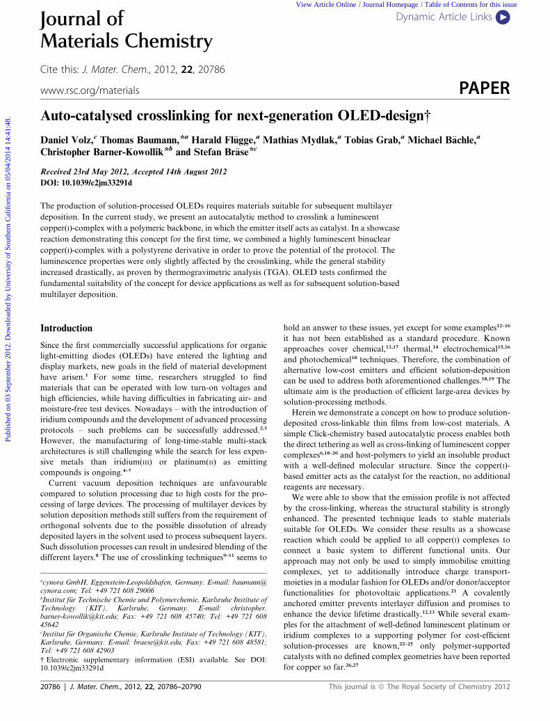
with three crystallographically non-equal ligands7 (Fig. 1).
A soluble, small-molecular model complex
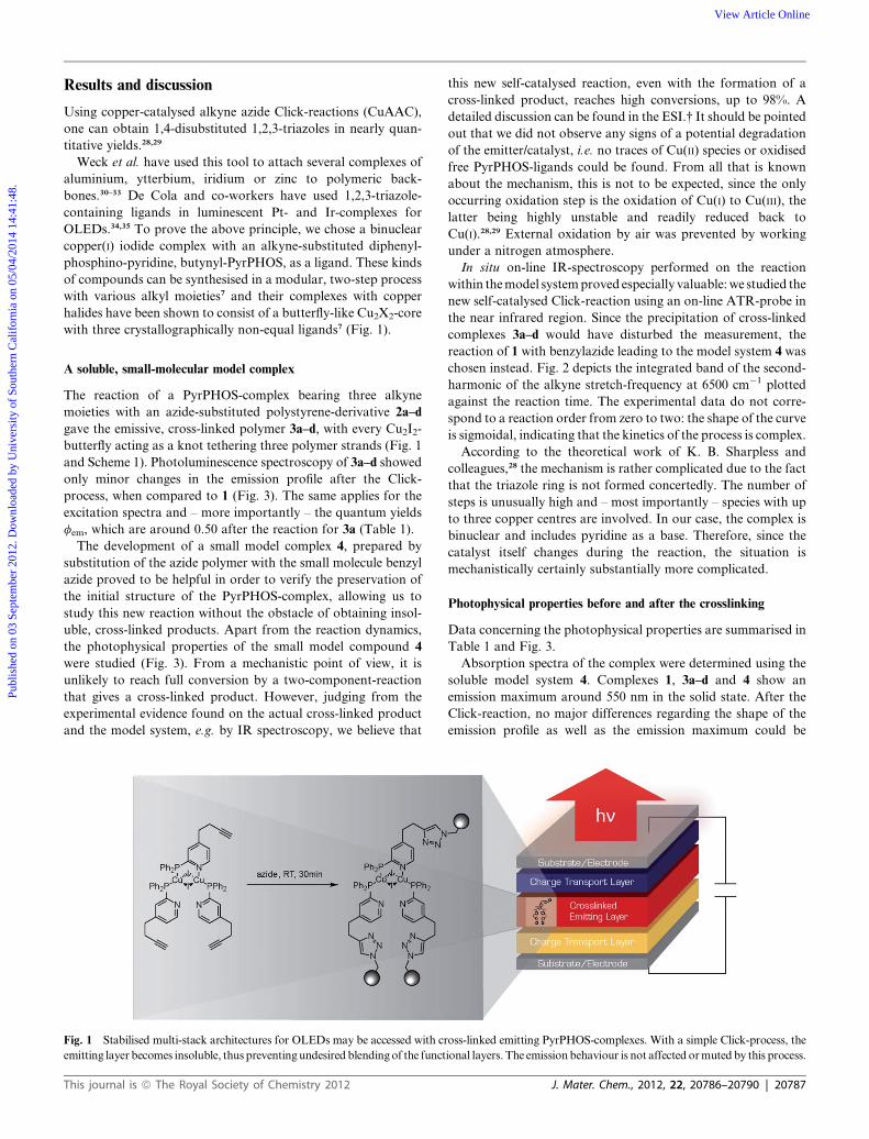
The reaction of a PyrPHOS-complex bearing three alkyne
moieties with an azide-substituted polystyrene-derivative 2a–d
gave the emissive, cross-linked polymer 3a–d, with every Cu2I2-
butterfly acting as a knot tethering three polymer strands (Fig. 1
and Scheme 1). Photoluminescence spectroscopy of 3a–d showed
only minor changes in the emission profile after the Click-
process, when compared to 1 (Fig. 3). The same applies for the
excitation spectra and – more importantly – the quantum yields
fem, which are around 0.50 after the reaction for 3a (Table 1).
The development of a small model complex 4, prepared by
substitution of the azide polymer with the small molecule benzyl
azide proved to be helpful in order to verify the preservation of
the initial structure of the PyrPHOS-complex, allowing us to
study this new reaction without the obstacle of obtaining insol-
uble, cross-linked products. Apart from the reaction dynamics,
the photophysical properties of the small model compound 4
were studied (Fig. 3). From a mechanistic point of view, it is
unlikely to reach full conversion by a two-component-reaction
that gives a cross-linked product. However, judging from the
experimental evidence found on the actual cross-linked product
and the model system, e.g. by IR spectroscopy, we believe that
Fig. 1 Stabilised multi-stack architectures for OLEDs may be accessed with cr
emitting layer becomes insoluble, thus preventingundesired blendingof the funct
This journal is ª The Royal Society of Chemistry 2012
this new self-catalysed reaction, even with the formation of a
cross-linked product, reaches high conversions, up to 98%. A
detailed discussion can be found in the ESI.† It should be pointed
out that we did not observe any signs of a potential degradation
of the emitter/catalyst, i.e. no traces of Cu(II) species or oxidised
free PyrPHOS-ligands could be found. From all that is known
about the mechanism, this is not to be expected, since the only
occurring oxidation step is the oxidation of Cu(I) to Cu(III), the
latter being highly unstable and readily reduced back to
Cu(I).28,29 External oxidation by air was prevented by working
under a nitrogen atmosphere.
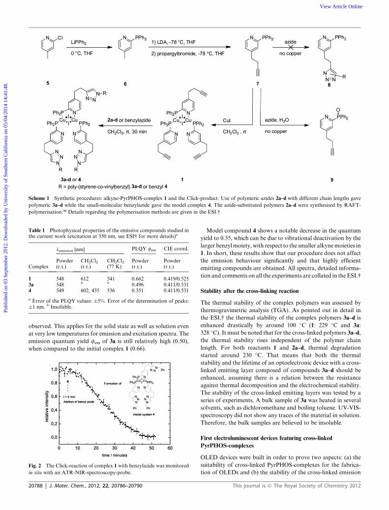
In situ on-line IR-spectroscopy performed on the reaction
within themodel systemproved especially valuable:we studied the
new self-catalysed Click-reaction using an on-line ATR-probe in
the near infrared region. Since the precipitation of cross-linked
complexes 3a–d would have disturbed the measurement, the
reaction of 1 with benzylazide leading to the model system 4 was
chosen instead. Fig. 2 depicts the integrated band of the second-
harmonic of the alkyne stretch-frequency at 6500 cm�1 plotted
against the reaction time. The experimental data do not corre-
spond to a reaction order from zero to two: the shape of the curve
is sigmoidal, indicating that the kinetics of the process is complex.
According to the theoretical work of K. B. Sharpless and
colleagues,28 the mechanism is rather complicated due to the fact
that the triazole ring is not formed concertedly. The number of
steps is unusually high and – most importantly – species with up
to three copper centres are involved. In our case, the complex is
binuclear and includes pyridine as a base. Therefore, since the
catalyst itself changes during the reaction, the situation is
mechanistically certainly substantially more complicated.
Photophysical properties before and after the crosslinking
Data concerning the photophysical properties are summarised in
Table 1 and Fig. 3.
Absorption spectra of the complex were determined using the
soluble model system 4. Complexes 1, 3a–d and 4 show an
emission maximum around 550 nm in the solid state. After the
Click-reaction, no major differences regarding the shape of the
emission profile as well as the emission maximum could be
oss-linked emitting PyrPHOS-complexes. With a simple Click-process, the
ional layers. The emissionbehaviour is not affected ormuted by this process.
J. Mater. Chem., 2012, 22, 20786–20790 | 20787
Scheme 1 Synthetic procedures: alkyne-PyrPHOS-complex 1 and the Click-product. Use of polymeric azides 2a–d with different chain lengths gave
polymeric 3a–d while the small-molecular benzylazide gave the model complex 4. The azide-substituted polymers 2a–d were synthesised by RAFT-
polymerisation.36 Details regarding the polymerisation methods are given in the ESI.†
Table 1 Photophysical properties of the emissive compounds studied inthe current work (excitation at 350 nm, see ESI† for more details)a
Complex
lemission [nm] PLQY fem CIE coord.
Powder(r.t.)
CH2Cl2(r.t.)
CH2Cl2(77 K)
Powder(r.t.)
Powder(r.t.)
1 548 612 541 0.662 0.419/0.5253a 548 b b 0.496 0.411/0.5314 549 602, 435 536 0.351 0.411/0.531
a Error of the PLQY values: �5%. Error of the determination of peaks:�1 nm. b Insoluble.
Publ
ishe
d on
03
Sept
embe
r 20
12. D
ownl
oade
d by
Uni
vers
ity o
f So
uthe
rn C
alif
orni
a on
05/
04/2
014
14:4
1:48
. View Article Online
observed. This applies for the solid state as well as solution even
at very low temperatures for emission and excitation spectra. The
emission quantum yield fem of 3a is still relatively high (0.50),
when compared to the initial complex 1 (0.66).
Fig. 2 The Click-reaction of complex 1 with benzylazide was monitored
in situ with an ATR-NIR-spectroscopy-probe.
20788 | J. Mater. Chem., 2012, 22, 20786–20790
Model compound 4 shows a notable decrease in the quantum
yield to 0.35, which can be due to vibrational deactivation by the
larger benzylmoiety, with respect to the smaller alkynemoieties in
1. In short, these results show that our procedure does not affect
the emission behaviour significantly and that highly efficient
emitting compounds are obtained. All spectra, detailed informa-
tion and comments on all the experiments are collated in the ESI.†
Stability after the cross-linking reaction
The thermal stability of the complex polymers was assessed by
thermogravimetric analysis (TGA). As pointed out in detail in
the ESI,† the thermal stability of the complex polymers 3a–d is
enhanced drastically by around 100 �C (1: 229 �C and 3a:
328 �C). It must be noted that for the cross-linked polymers 3a–d,
the thermal stability rises independent of the polymer chain
length. For both reactants 1 and 2a–d, thermal degradation
started around 230 �C. That means that both the thermal
stability and the lifetime of an optoelectronic device with a cross-
linked emitting layer composed of compounds 3a–d should be
enhanced, assuming there is a relation between the resistance
against thermal decomposition and the electrochemical stability.
The stability of the cross-linked emitting layers was tested by a
series of experiments. A bulk sample of 3a was heated in several
solvents, such as dichloromethane and boiling toluene. UV-VIS-
spectroscopy did not show any traces of the material in solution.
Therefore, the bulk samples are believed to be insoluble.
First electroluminescent devices featuring cross-linked
PyrPHOS-complexes
OLED devices were built in order to prove two aspects: (a) the
suitability of cross-linked PyrPHOS-complexes for the fabrica-
tion of OLEDs and (b) the stability of the cross-linked emission
This journal is ª The Royal Society of Chemistry 2012
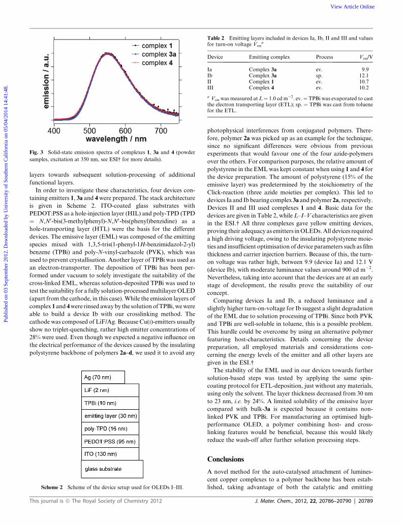
Fig. 3 Solid-state emission spectra of complexes 1, 3a and 4 (powder
samples, excitation at 350 nm, see ESI† for more details).
Table 2 Emitting layers included in devices Ia, Ib, II and III and valuesfor turn-on voltage Von
a
Device Emitting complex Process Von/V
Ia Complex 3a ev. 9.9Ib Complex 3a sp. 12.1II Complex 1 ev. 10.7III Complex 4 ev. 10.2
a Von was measured at L¼ 1.0 cd m�2. ev.¼ TPBi was evaporated to castthe electron transporting layer (ETL); sp. ¼ TPBi was cast from toluenefor the ETL.
Publ
ishe
d on
03
Sept
embe
r 20
12. D
ownl
oade
d by
Uni
vers
ity o
f So
uthe
rn C
alif
orni
a on
05/
04/2
014
14:4
1:48
. View Article Online
layers towards subsequent solution-processing of additional
functional layers.
In order to investigate these characteristics, four devices con-
taining emitters 1, 3a and 4were prepared. The stack architecture
is given in Scheme 2. ITO-coated glass substrates with
PEDOT:PSS as a hole-injection layer (HIL) and poly-TPD (TPD
¼ N,N0-bis(3-methylphenyl)-N,N0-bis(phenyl)benzidine) as a
hole-transporting layer (HTL) were the basis for the different
devices. The emissive layer (EML) was composed of the emitting
species mixed with 1,3,5-tris(1-phenyl-1H-benzimidazol-2-yl)
benzene (TPBi) and poly-N-vinyl-carbazole (PVK), which was
used to prevent crystallisation. Another layer of TPBi was used as
an electron-transporter. The deposition of TPBi has been per-
formed under vacuum to solely investigate the suitability of the
cross-linked EML, whereas solution-deposited TPBi was used to
test the suitability for a fully solution-processedmultilayerOLED
(apart from the cathode, in this case).While the emission layers of
complex 1 and 4were rinsed awayby the solution ofTPBi,wewere
able to build a device Ib with our crosslinking method. The
cathode was composed of LiF/Ag. Because Cu(I)-emitters usually
show no triplet-quenching, rather high emitter concentrations of
28% were used. Even though we expected a negative influence on
the electrical performance of the devices caused by the insulating
polystyrene backbone of polymers 2a–d, we used it to avoid any
Scheme 2 Scheme of the device setup used for OLEDs I–III.
This journal is ª The Royal Society of Chemistry 2012
photophysical interferences from conjugated polymers. There-
fore, polymer 2a was picked up as an example for the technique,
since no significant differences were obvious from previous
experiments that would favour one of the four azide-polymers
over the others. For comparison purposes, the relative amount of
polystyrene in the EMLwas kept constant when using 1 and 4 for
the device preparation. The amount of polystyrene (15% of the
emissive layer) was predetermined by the stoichiometry of the
Click-reaction (three azide moieties per complex). This led to
devices Ia and Ibbearing complex 3a andpolymer2a, respectively.
Devices II and III used complexes 1 and 4. Basic data for the
devices are given in Table 2, while L–I–V characteristics are given
in the ESI.† All three complexes gave yellow emitting devices,
proving their adequacy as emitters inOLEDs.All devices required
a high driving voltage, owing to the insulating polystyrene moie-
ties and insufficient optimisation of device parameters such as film
thickness and carrier injection barriers. Because of this, the turn-
on voltage was rather high, between 9.9 (device Ia) and 12.1 V
(device Ib), with moderate luminance values around 900 cd m�2.
Nevertheless, taking into account that the devices are at an early
stage of development, the results prove the suitability of our
concept.
Comparing devices Ia and Ib, a reduced luminance and a
slightly higher turn-on-voltage for Ib suggest a slight degradation
of the EML due to solution processing of TPBi. Since both PVK
and TPBi are well-soluble in toluene, this is a possible problem.
This hurdle could be overcome by using an alternative polymer
featuring host-characteristics. Details concerning the device
preparation, all employed materials and considerations con-
cerning the energy levels of the emitter and all other layers are
given in the ESI.†
The stability of the EML used in our devices towards further
solution-based steps was tested by applying the same spin-
coating protocol for ETL-deposition, just without any materials,
using only the solvent. The layer thickness decreased from 30 nm
to 23 nm, i.e. by 24%. A limited solubility of the emissive layer
compared with bulk-3a is expected because it contains non-
linked PVK and TPBi. For manufacturing an optimised high-
performance OLED, a polymer combining host- and cross-
linking features would be beneficial, because this would likely
reduce the wash-off after further solution processing steps.
Conclusions
A novel method for the auto-catalysed attachment of lumines-
cent copper complexes to a polymer backbone has been estab-
lished, taking advantage of both the catalytic and emitting
J. Mater. Chem., 2012, 22, 20786–20790 | 20789
Publ
ishe
d on
03
Sept
embe
r 20
12. D
ownl
oade
d by
Uni
vers
ity o
f So
uthe
rn C
alif
orni
a on
05/
04/2
014
14:4
1:48
. View Article Online
properties of copper(I) complexes. As a showcase reaction,
binuclear copper complexes with PyrPHOS-ligands and small
polymeric azides were coupled. These systems show a bright
emission at 550 nm, quantum efficiencies of 50% and are suitable
as emitters for organic light emitting diodes. In addition, it has
been demonstrated that the thermal stability is enhanced signif-
icantly by the cross-linking process. With the aid of the current
method, we were able to build several devices with solvent-
resistant emissive layers for solution processed OLEDs.
Outlook
In order to prepare an optimised OLED device, we are working
on a modified procedure. The concept is not limited to the
polymers 2a–d, which are insulating polystyrene derivatives.
These polymers are considered to be the main cause of the high
turn-on voltages of our test devices. An azide-functionalised host
polymer, bearing charge-transporting carbazole-units for
example, would be preferable in an optimised device and would
further prevent the layer degradation by solution processing of
the ETL, because no small molecules would be required in the
final device anymore. However, we chose polystyrene for its
manifold chemistry as a general example, rather than presenting
a highly specialised niche-polymer optimised only for a single
copper complex and we were still able to build working electro-
luminescent devices.
Acknowledgements
Atomic absorption spectroscopy (copper) was carried out by
Zsolt Berner and Gesine Preuß. The thermogravimetric analysis
(TGA) measurements were carried out at the Fraunhofer ICT in
Pfinztal with help from J€ordis Eisenbl€atter and Dr. Leonie
Barner. We thank Manuela Wallesch for formatting the manu-
script. We acknowledge the Karlsruhe Institute of Technology
(KIT) for continued support in the context of the Excellence
Initiative for leading German universities. Financial support
from the Verband der Chemischen Industrie (VCI) and the
Deutsche Forschungsgemeinschaft (DFG) via support for the
transregional collaborative research centre SFB/TRR 88
‘‘3MET’’ are additionally acknowledged.
References
1 S. Reineke, F. Lindner, G. Schwartz, N. Seidler, K. Walzer,B. L€ussem and K. Leo, Nature, 2009, 459, 234–238.
2 A. B. Tamayo, S. Garon, T. Sajoto, P. I. Djurovich, I. M. Tsyba,R. Bau and M. E. Thompson, Inorg. Chem., 2005, 44, 8723–8732.
3 S. Olthof, R. Meerheim, M. Schober and K. Leo, Phys. Rev. B:Condens. Matter Mater. Phys., 2009, 79, 245308–245315.
4 N. Armaroli, G. Accorsi, F. Cardinali and A. Lostorti, Top. Curr.Chem., 2007, 280, 69–115.
5 M. Hashimoto, S. Igawa, M. Yashima, I. Kawata, M. Hoshino andM. Osawa, J. Am. Chem. Soc., 2011, 133, 10348–10351.
20790 | J. Mater. Chem., 2012, 22, 20786–20790
6 D. M. Zink, T. Grab, T. Baumann, M. Nieger, E. C. Barnes,W. Klopper and S. Br€ase, Organometallics, 2011, 30, 3275–3283.
7 D. M. Zink, M. B€achle, T. Baumann, M. Nieger, M. K€uhn, C. Wang,W. Klopper, U. Monkowius, T. Hofbeck, H. Yersin and S. Br€ase,Inorg. Chem., 2012, submitted.
8 A. R. G. Smith, K. H. Lee, A. Nelson, M. James, P. L. Burn andI. R. Gentle, Adv. Mater., 2012, 24, 822–826.
9 C. a. Zuniga, S. Barlow and S. R. Marder, Chem. Mater., 2011, 23,658–681.
10 O. Nuyken, S. Jungermann, V. Wiederhirn, E. Bacher andK. Meerholz, Monatsh. Chem., 2006, 137, 811–824.
11 O. Nuyken, E. Bacher, T. Braig, R. F�aber, F. Mielke, M. Rojahn,V. Wiederhirn, K. Meerholz and D. M€uller, Des. MonomersPolym., 2002, 5, 195–210.
12 M. C. Gather, A. K€ohnen, A. Falcou, H. Becker and K. Meerholz,Adv. Funct. Mater., 2007, 17, 191–200.
13 A. K€ohnen, N. Riegel, J. H.-W. M. Kremer, H. Lademann,D. C. M€uller and K. Meerholz, Adv. Mater., 2009, 21, 879–884.
14 C. Zhong, S. Liu, F. Huang, H. Wu and Y. Cao, Chem. Mater., 2011,23, 4870–4876.
15 C. Gu, T. Fei, L. Yao, Y. Lv, D. Lu andY.Ma,Adv.Mater., 2011, 23,527–530.
16 A. Baba, K. Onishi, W. Knoll and R. C. Advincula, J. Phys. Chem. B,2004, 108, 18949–18955.
17 I. O. Huyal, U. Koldemir, T. Ozel, H. V. Demir and D. Tuncel, J.Mater. Chem., 2008, 18, 3568.
18 H. Yersin, A. F. Rausch, R. Czerwieniec, T. Hofbeck and T. Fischer,Coord. Chem. Rev., 2011, 255, 2622–2652.
19 R. Czerwieniec, J. Yu and H. Yersin, Inorg. Chem., 2011, 50, 8293–8301.
20 D.M. Zink, T. Baumann,M. Nieger and S. Br€ase, Eur. J. Org. Chem.,2011, 1432–1437.
21 B. O’Regan and M. Gr€atzel, Nature, 1991, 353, 737–740.22 P. T. Furuta, L. Deng, S. Garon, M. E. Thompson and
J. M. J. Fr�echet, J. Am. Chem. Soc., 2004, 126, 15388–15389.23 H. Gao, D. A. Poulsen, B. Ma, D. A. Unruh, X. Zhao, J. E. Millstone
and J. M. J. Fr�echet, Nano Lett., 2010, 10, 1440–1444.24 B. Ma, F. Lauterwasser, L. Deng, C. S. Zonte, B. J. Kim,
J. M. J. Fr�echet, C. Borek and M. E. Thompson, Chem. Mater.,2007, 19, 4827–4832.
25 X.-Y. Wang, A. Kimyonok and M. Weck, Chem. Commun., 2006,3933–3935.
26 U. Sirion, Y. J. Bae, B. Lee and D. Chi, Synlett, 2008, 2326–2330.27 U. Castro, D. C. Sherrington, A. Fortuny, A. Fabregat, F. St€uber,
J. Font and C. Bengoa, Catal. Today, 2010, 157, 66–70.28 F. Himo, T. Lovell, R. Hilgraf, V. V. Rostovtsev, L. Noodleman,
K. B. Sharpless and V. V. Fokin, J. Am. Chem. Soc., 2005, 127,210–216.
29 M. Meldal and C. W. Tornøe, Chem. Rev., 2008, 108, 2952–3015.30 A. Kimyonok, X. Wang and M. Weck, J. Macromol. Sci., Part C,
2006, 46, 47–77.31 A. Meyers, A. Kimyonok and M. Weck, Macromolecules, 2005, 38,
8671–8678.32 A. Meyers and M. Weck, Chem. Mater., 2004, 16, 1183–1188.33 A. Meyers and M. Weck, Macromolecules, 2003, 36, 1766–1768.34 I. Stengel, C. A. Strassert, E. A. Plummer, C.-H. Chien, L. De Cola
and P. B€auerle, Eur. J. Inorg. Chem., 2012, 1795–1809.35 S. Zanarini, M. Felici, G. Valenti, M. Marcaccio, L. Prodi,
S. Bonacchi, P. Contreras-Carballada, R. M. Williams,M. C. Feiters, R. J. M. Nolte, L. De Cola and F. Paolucci, Chem.–Eur. J., 2011, 17, 4640–4647.
36 G. Moad and C. Barner-Kowollik, in Handbook of RAFT-Polymerization, ed. C. Barner-Kowollik, Wiley-VCH, Weinheim,Germany, 1st ed., 2008.
This journal is ª The Royal Society of Chemistry 2012