Embed Size (px)
Citation preview
w WM5102S
Audio Hub CODEC with Master Hi-Fi DSP
WOLFSON MICROELECTRONICS plc Product Preview, April 2014, Rev 1.1
[1] This product is protected by Patents US 7,622,984, US 7,626,445, US 7,765,019 and GB 2,432,765
Copyright 2014 Wolfson Microelectronics plc
DESCRIPTION
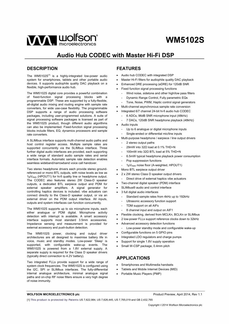
The WM5102S[1] is a highly-integrated low-power audio system for smartphones, tablets and other portable audio devices. It supports audiophile quality DAC playback on a flexible, high-performance audio hub.
The WM5102S digital core provides a powerful combination of fixed-function signal processing blocks with a programmable DSP. These are supported by a fully-flexible, all-digital audio mixing and routing engine with sample rate converters, for wide use-case flexibility. The programmable DSP supports a range of audio processing software packages, including user-programmed solutions. A suite of signal processing software packages is licensed as part of the WM5102S product, though different audio algorithms can also be implemented. Fixed-function signal processing blocks include filters, EQ, dynamics processors and sample rate converters.
A SLIMbus interface supports multi-channel audio paths and host control register access. Multiple sample rates are supported concurrently via the SLIMbus interface. Three further digital audio interfaces are provided, each supporting a wide range of standard audio sample rates and serial interface formats. Automatic sample rate detection enables seamless wideband/narrowband voice call handover.
Two stereo headphone drivers each provide stereo ground-referenced or mono BTL outputs, with noise levels as low as 1µVRMS (HPOUT1) for hi-fi quality line or headphone output. The CODEC also features stereo 2W Class-D speaker outputs, a dedicated BTL earpiece output and PDM for external speaker amplifiers. A signal generator for controlling haptics devices is included; vibe actuators can connect directly to the Class-D speaker output, or via an external driver on the PDM output interface. All inputs, outputs and system interfaces can function concurrently.
The WM5102S supports up to six microphone inputs, each either analogue or PDM digital. Microphone activity detection with interrupt is available. A smart accessory interface supports most standard 3.5mm accessories. Impedance sensing and measurement is provided for external accessory and push-button detection.
The WM5102S power, clocking and output driver architectures are all designed to maximise battery life in voice, music and standby modes. Low-power ‘Sleep’ is supported, with configurable wake-up events. The WM5102S is powered from a 1.8V external supply. A separate supply is required for the Class D speaker drivers (typically direct connection to 4.2V battery).
Two integrated FLLs provide support for a wide range of system clock frequencies. The WM5102S is configured using the I2C, SPI or SLIMbus interfaces. The fully-differential internal analogue architecture, minimal analogue signal paths and on-chip RF noise filters ensure a very high degree of noise immunity.
FEATURES Audio hub CODEC with integrated DSP
Master Hi-Fi filters for audiophile quality DAC playback
Enhanced DRE processing (eDRE) for 120dB SNR
Fixed function signal processing functions
- Wind noise, sidetone and other high/low pass filters
- Dynamic Range Control, Fully parametric EQs
- Tone, Noise, PWM, Haptic control signal generators
Multi-channel asynchronous sample rate conversion
Integrated 6/7 channel 24-bit hi-fi audio hub CODEC
- 6 ADCs, 96dB SNR microphone input (48kHz)
- 7 DACs, 120dB SNR headphone playback (48kHz)
Audio inputs
- Up to 6 analogue or digital microphone inputs
- Single-ended or differential mic/line inputs
Multi-purpose headphone / earpiece / line output drivers
- 2 stereo output paths
- 29mW into 32Ω load at 0.1% THD+N
- 100mW into 32Ω BTL load at 5% THD+N
- 6.5mW typical headphone playback power consumption
- Pop suppression functions
- 1µVRMS noise floor (A-weighted, HPOUT1)
Mono BTL earpiece output driver
2 x 2W stereo Class D speaker output drivers
- Direct drive of external haptics vibe actuators
Two-channel digital speaker (PDM) interface
SLIMbus® audio and control interface
3 full digital audio interfaces
- Standard sample rates from 4kHz up to 192kHz
- Ultrasonic accessory function support
- TDM support on all AIFs
- 8 channel input and output on AIF1
Flexible clocking, derived from MCLKn, BCLKn or SLIMbus
2 low-power FLLs support reference clocks down to 32kHz
Advanced accessory detection functions
- Low-power standby mode and configurable wake-up
Configurable functions on 5 GPIO pins
Integrated LDO regulators and charge pumps
Support for single 1.8V supply operation
Small W-CSP package, 0.4mm pitch
APPLICATIONS Smartphones and Multimedia handsets
Tablets and Mobile Internet Devices (MID)
Portable Music Players (PMP)
WM5102S Product Preview
w PP, April 2014, Rev 1.1
2
BLOCK DIAGRAM

Product Preview WM5102S
w PP, April 2014, Rev 1.1
3
TABLE OF CONTENTS
DESCRIPTION ................................................................................................................ 1 FEATURES ..................................................................................................................... 1 APPLICATIONS .............................................................................................................. 1 BLOCK DIAGRAM ......................................................................................................... 2 TABLE OF CONTENTS .................................................................................................. 3 PIN CONFIGURATION ................................................................................................... 7 ORDERING INFORMATION ........................................................................................... 7 PIN DESCRIPTION ......................................................................................................... 8 ABSOLUTE MAXIMUM RATINGS ............................................................................... 13 RECOMMENDED OPERATING CONDITIONS ............................................................ 14 ELECTRICAL CHARACTERISTICS ............................................................................ 15
TERMINOLOGY ......................................................................................................................... 26 THERMAL CHARACTERISTICS .................................................................................. 27 TYPICAL PERFORMANCE .......................................................................................... 28
TYPICAL POWER CONSUMPTION ......................................................................................... 28 TYPICAL SIGNAL LATENCY .................................................................................................... 29
SIGNAL TIMING REQUIREMENTS ............................................................................. 30 SYSTEM CLOCK & FREQUENCY LOCKED LOOP (FLL) ....................................................... 30 AUDIO INTERFACE TIMING ..................................................................................................... 32
DIGITAL MICROPHONE (DMIC) INTERFACE TIMING ................................................................................................................ 32 DIGITAL SPEAKER (PDM) INTERFACE TIMING ......................................................................................................................... 33 DIGITAL AUDIO INTERFACE - MASTER MODE ......................................................................................................................... 34 DIGITAL AUDIO INTERFACE - SLAVE MODE ............................................................................................................................. 35 DIGITAL AUDIO INTERFACE - TDM MODE ................................................................................................................................ 36
CONTROL INTERFACE TIMING .............................................................................................. 37 2-WIRE (I2C) CONTROL MODE ................................................................................................................................................... 37 4-WIRE (SPI) CONTROL MODE ................................................................................................................................................... 38
SLIMBUS INTERFACE TIMING ................................................................................................ 39 DEVICE DESCRIPTION ............................................................................................... 41
INTRODUCTION ........................................................................................................................ 41 HI-FI AUDIO CODEC ..................................................................................................................................................................... 41 DIGITAL AUDIO CORE ................................................................................................................................................................. 42 DIGITAL INTERFACES ................................................................................................................................................................. 42 OTHER FEATURES ...................................................................................................................................................................... 43
INPUT SIGNAL PATH ................................................................................................................ 44 ANALOGUE MICROPHONE INPUT ............................................................................................................................................. 45 ANALOGUE LINE INPUT .............................................................................................................................................................. 46 DIGITAL MICROPHONE INPUT ................................................................................................................................................... 46 INPUT SIGNAL PATH ENABLE .................................................................................................................................................... 48 INPUT SIGNAL PATH SAMPLE RATE CONTROL ....................................................................................................................... 49 INPUT SIGNAL PATH CONFIGURATION .................................................................................................................................... 49 INPUT SIGNAL PATH DIGITAL VOLUME CONTROL .................................................................................................................. 53 DIGITAL MICROPHONE INTERFACE PULL-DOWN ................................................................................................................... 57
DIGITAL CORE .......................................................................................................................... 58 DIGITAL CORE MIXERS ............................................................................................................................................................... 60 DIGITAL CORE INPUTS ............................................................................................................................................................... 63 DIGITAL CORE OUTPUT MIXERS ............................................................................................................................................... 64 MIC MUTE MIXER ......................................................................................................................................................................... 67 5-BAND PARAMETRIC EQUALISER (EQ) ................................................................................................................................... 68 DYNAMIC RANGE CONTROL (DRC) ........................................................................................................................................... 73 LOW PASS / HIGH PASS DIGITAL FILTER (LHPF) ..................................................................................................................... 83
WM5102S Product Preview
w PP, April 2014, Rev 1.1
4
DIGITAL CORE DSP ..................................................................................................................................................................... 86 TONE GENERATOR ..................................................................................................................................................................... 88 NOISE GENERATOR .................................................................................................................................................................... 90 HAPTIC SIGNAL GENERATOR .................................................................................................................................................... 91 PWM GENERATOR ...................................................................................................................................................................... 94 SAMPLE RATE CONTROL ........................................................................................................................................................... 96 ASYNCHRONOUS SAMPLE RATE CONVERTER (ASRC) ....................................................................................................... 104 ISOCHRONOUS SAMPLE RATE CONVERTER (ISRC) ............................................................................................................ 107
DSP FIRMWARE CONTROL .................................................................................................. 111 DSP FIRMWARE MEMORY CONTROL ..................................................................................................................................... 111 DSP FIRMWARE EXECUTION ................................................................................................................................................... 114 DSP DIRECT MEMORY ACCESS (DMA) CONTROL ................................................................................................................ 114 DSP DEBUG SUPPORT ............................................................................................................................................................. 116
DIGITAL AUDIO INTERFACE ................................................................................................. 117 MASTER AND SLAVE MODE OPERATION ............................................................................................................................... 118 AUDIO DATA FORMATS ............................................................................................................................................................ 118 AIF TIMESLOT CONFIGURATION ............................................................................................................................................. 120 TDM OPERATION BETWEEN THREE OR MORE DEVICES .................................................................................................... 122
DIGITAL AUDIO INTERFACE CONTROL .............................................................................. 124 AIF SAMPLE RATE CONTROL ................................................................................................................................................... 124 AIF MASTER / SLAVE CONTROL .............................................................................................................................................. 124 AIF SIGNAL PATH ENABLE ....................................................................................................................................................... 128 AIF BCLK AND LRCLK CONTROL ............................................................................................................................................. 130 AIF DIGITAL AUDIO DATA CONTROL ....................................................................................................................................... 134 AIF TDM AND TRI-STATE CONTROL ........................................................................................................................................ 137 AIF DIGITAL PULL-UP AND PULL-DOWN ................................................................................................................................. 138
SLIMBUS INTERFACE ............................................................................................................ 140 SLIMBUS DEVICES .................................................................................................................................................................... 140 SLIMBUS FRAME STRUCTURE ................................................................................................................................................ 140 CONTROL SPACE ...................................................................................................................................................................... 140 DATA SPACE .............................................................................................................................................................................. 141
SLIMBUS CONTROL SEQUENCES ....................................................................................... 142 DEVICE MANAGEMENT & CONFIGURATION .......................................................................................................................... 142 INFORMATION MANAGEMENT ................................................................................................................................................. 142 VALUE MANAGEMENT (INCLUDING REGISTER ACCESS) .................................................................................................... 143 FRAME & CLOCKING MANAGEMENT ...................................................................................................................................... 143 DATA CHANNEL CONFIGURATION .......................................................................................................................................... 144
SLIMBUS INTERFACE CONTROL ......................................................................................... 145 SLIMBUS DEVICE PARAMETERS ............................................................................................................................................. 145 SLIMBUS MESSAGE SUPPORT ................................................................................................................................................ 145 SLIMBUS PORT NUMBER CONTROL ....................................................................................................................................... 148 SLIMBUS SAMPLE RATE CONTROL ........................................................................................................................................ 148 SLIMBUS SIGNAL PATH ENABLE ............................................................................................................................................. 149 SLIMBUS CONTROL REGISTER ACCESS ............................................................................................................................... 150 SLIMBUS CLOCKING CONTROL ............................................................................................................................................... 152
OUTPUT SIGNAL PATH .......................................................................................................... 154 OUTPUT SIGNAL PATH ENABLE .............................................................................................................................................. 156 OUTPUT SIGNAL PATH SAMPLE RATE CONTROL ................................................................................................................. 157 OUTPUT SIGNAL PATH CONTROL ........................................................................................................................................... 158 OUTPUT SIGNAL PATH DIGITAL VOLUME CONTROL ............................................................................................................ 161 OUTPUT SIGNAL PATH DIGITAL VOLUME LIMIT .................................................................................................................... 166 OUTPUT SIGNAL PATH NOISE GATE CONTROL .................................................................................................................... 170 OUTPUT SIGNAL PATH AEC LOOPBACK ................................................................................................................................ 172 HEADPHONE/EARPIECE OUTPUTS AND MONO MODE ........................................................................................................ 173 SPEAKER OUTPUTS (ANALOGUE) .......................................................................................................................................... 175 SPEAKER OUTPUTS (DIGITAL PDM) ....................................................................................................................................... 175
Product Preview WM5102S
w PP, April 2014, Rev 1.1
5
EXTERNAL ACCESSORY DETECTION ................................................................................ 178 JACK DETECT ............................................................................................................................................................................ 178 JACK POP SUPPRESSION (MICDET CLAMP) .......................................................................................................................... 180 MICROPHONE DETECT ............................................................................................................................................................. 181 HEADPHONE DETECT ............................................................................................................................................................... 186
LOW POWER SLEEP CONFIGURATION .............................................................................. 190 SLEEP MODE .............................................................................................................................................................................. 190 SLEEP CONTROL SIGNALS - JD1, GP5, MICDET CLAMP ...................................................................................................... 193 WAKE-UP TRANSITION ............................................................................................................................................................. 195 WRITE SEQUENCE CONTROL .................................................................................................................................................. 196 INTERRUPT CONTROL .............................................................................................................................................................. 196
GENERAL PURPOSE INPUT / OUTPUT ............................................................................... 197 GPIO CONTROL ......................................................................................................................................................................... 198 GPIO FUNCTION SELECT ......................................................................................................................................................... 200 DIGITAL AUDIO INTERFACE FUNCTION (AIFNTXLRCLK) ...................................................................................................... 203 BUTTON DETECT (GPIO INPUT) ............................................................................................................................................... 204 LOGIC ‘1’ AND LOGIC ‘0’ OUTPUT (GPIO OUTPUT) ................................................................................................................ 204 INTERRUPT (IRQ) STATUS OUTPUT ........................................................................................................................................ 204 DSP STATUS FLAG (DSP IRQN) OUTPUT ............................................................................................................................... 205 OPCLK AND OPCLK_ASYNC CLOCK OUTPUT ....................................................................................................................... 205 FREQUENCY LOCKED LOOP (FLL) STATUS OUTPUT ........................................................................................................... 206 FREQUENCY LOCKED LOOP (FLL) CLOCK OUTPUT ............................................................................................................. 207 PULSE WIDTH MODULATION (PWM) SIGNAL OUTPUT ......................................................................................................... 207 HEADPHONE DETECTION STATUS OUTPUT ......................................................................................................................... 208 MICROPHONE / ACCESSORY DETECTION STATUS OUTPUT .............................................................................................. 208 ASYNCHRONOUS SAMPLE RATE CONVERTER (ASRC) LOCK STATUS OUTPUT ............................................................. 208 ASYNCHRONOUS SAMPLE RATE CONVERTER (ASRC) CONFIGURATION ERROR STATUS OUTPUT ........................... 209 OVER-TEMPERATURE STATUS OUTPUT ............................................................................................................................... 209 DYNAMIC RANGE CONTROL (DRC) STATUS OUTPUT .......................................................................................................... 209 CONTROL WRITE SEQUENCER STATUS OUTPUT ................................................................................................................ 210 CONTROL INTERFACE ERROR STATUS OUTPUT ................................................................................................................. 210 SYSTEM CLOCKS ENABLE STATUS OUTPUT ........................................................................................................................ 210 CLOCKING ERROR STATUS OUTPUT ..................................................................................................................................... 211 DIGITAL AUDIO INTERFACE CONFIGURATION ERROR STATUS OUTPUT ......................................................................... 212
INTERRUPTS .......................................................................................................................... 213 CLOCKING AND SAMPLE RATES ......................................................................................... 225
SYSTEM CLOCKING .................................................................................................................................................................. 225 SAMPLE RATE CONTROL ......................................................................................................................................................... 225 AUTOMATIC SAMPLE RATE DETECTION ................................................................................................................................ 226 SYSCLK AND ASYNCCLK CONTROL ....................................................................................................................................... 227 MISCELLANEOUS CLOCK CONTROLS .................................................................................................................................... 230 BCLK AND LRCLK CONTROL .................................................................................................................................................... 237 CONTROL INTERFACE CLOCKING .......................................................................................................................................... 237 FREQUENCY LOCKED LOOP (FLL) .......................................................................................................................................... 238 FREE-RUNNING FLL MODE ...................................................................................................................................................... 248 SPREAD SPECTRUM FLL CONTROL ....................................................................................................................................... 249 GPIO OUTPUTS FROM FLL ....................................................................................................................................................... 250 EXAMPLE FLL CALCULATION ................................................................................................................................................... 250 EXAMPLE FLL SETTINGS .......................................................................................................................................................... 251
CONTROL INTERFACE .......................................................................................................... 252 2-WIRE (I2C) CONTROL MODE ................................................................................................................................................. 253 4-WIRE (SPI) CONTROL MODE ................................................................................................................................................. 257
CONTROL WRITE SEQUENCER ........................................................................................... 258 INITIATING A SEQUENCE .......................................................................................................................................................... 258 AUTOMATIC SAMPLE RATE DETECTION SEQUENCES ........................................................................................................ 259 JACK DETECT, GPIO, MICDET CLAMP, AND WAKE-UP SEQUENCES ................................................................................. 260
WM5102S Product Preview
w PP, April 2014, Rev 1.1
6
DRC SIGNAL DETECT SEQUENCES ........................................................................................................................................ 262 SEQUENCER OUTPUTS AND READBACK ............................................................................................................................... 263 PROGRAMMING A SEQUENCE ................................................................................................................................................ 263 SEQUENCER MEMORY DEFINITION ........................................................................................................................................ 264
CHARGE PUMPS, REGULATORS AND VOLTAGE REFERENCE ...................................... 266 CHARGE PUMPS AND LDO2 REGULATOR ............................................................................................................................. 266 MICBIAS BIAS (MICBIAS) CONTROL ........................................................................................................................................ 266 VOLTAGE REFERENCE CIRCUIT ............................................................................................................................................. 267 LDO1 REGULATOR AND DCVDD SUPPLY ............................................................................................................................... 267 BLOCK DIAGRAM AND CONTROL REGISTERS ...................................................................................................................... 268
JTAG INTERFACE ................................................................................................................... 273 THERMAL SHUTDOWN .......................................................................................................... 273 POWER-ON RESET (POR) AND HARDWARE RESET ........................................................ 274 SOFTWARE RESET, WAKE-UP, AND DEVICE ID ................................................................ 277
REGISTER MAP ......................................................................................................... 279 APPLICATIONS INFORMATION ............................................................................... 314
RECOMMENDED EXTERNAL COMPONENTS ..................................................................... 314 ANALOGUE INPUT PATHS ........................................................................................................................................................ 314 DIGITAL MICROPHONE INPUT PATHS .................................................................................................................................... 314 MICROPHONE BIAS CIRCUIT ................................................................................................................................................... 315 HEADPHONE/EARPIECE DRIVER OUTPUT PATH .................................................................................................................. 316 SPEAKER DRIVER OUTPUT PATH ........................................................................................................................................... 318 POWER SUPPLY / REFERENCE DECOUPLING ...................................................................................................................... 320 CHARGE PUMP COMPONENTS ............................................................................................................................................... 321 EXTERNAL ACCESSORY DETECTION COMPONENTS .......................................................................................................... 321 RECOMMENDED EXTERNAL COMPONENTS DIAGRAM ....................................................................................................... 323
RESETS SUMMARY ............................................................................................................... 324 DIGITAL AUDIO INTERFACE CLOCKING CONFIGURATIONS ........................................... 325 PCB LAYOUT CONSIDERATIONS ......................................................................................... 329
PACKAGE DIMENSIONS ........................................................................................... 330 IMPORTANT NOTICE ................................................................................................ 331
ADDRESS: ............................................................................................................................... 331 REVISION HISTORY .................................................................................................. 332
Product Preview WM5102S
w PP, April 2014, Rev 1.1
7
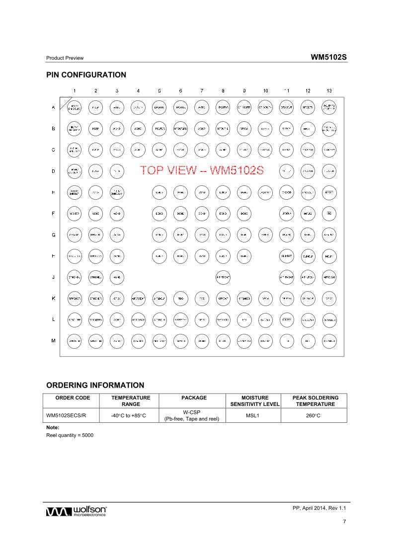
PIN CONFIGURATION
ORDERING INFORMATION
ORDER CODE TEMPERATURE RANGE
PACKAGE MOISTURE SENSITIVITY LEVEL
PEAK SOLDERING TEMPERATURE
WM5102SECS/R -40C to +85C W-CSP
(Pb-free, Tape and reel) MSL1 260C
Note:
Reel quantity = 5000

WM5102S Product Preview
w PP, April 2014, Rev 1.1
8
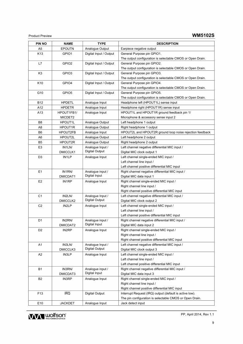
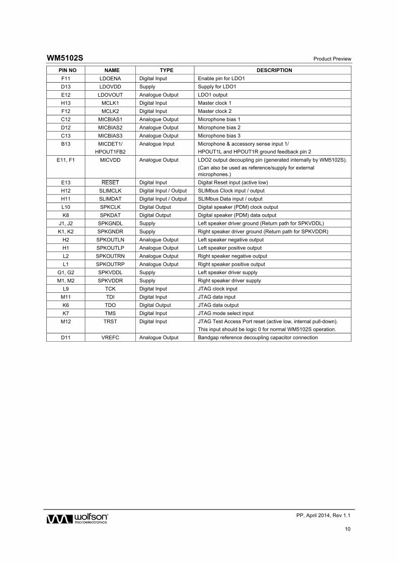
PIN DESCRIPTION
A description of each pin on the WM5102S is provided below.
Note that a table detailing the associated power domain for every input and output pin is provided on the following page.
Note that, where multiple pins share a common name, these pins should be tied together on the PCB.
All Digital Output pins are CMOS outputs, unless otherwise stated.
PIN NO NAME TYPE DESCRIPTION
B3, B4, B7, C3, C4, C5, C6, C7, C8, F2, F3, G3, H3, J3, L3
AGND Supply Analogue ground (Return path for AVDD)
J13 AIF1BCLK Digital Input / Output Audio interface 1 bit clock
J11 AIF1RXDAT Digital Input Audio interface 1 RX digital audio data
J12 AIF1LRCLK Digital Input / Output Audio interface 1 left / right clock
J8 AIF1TXDAT Digital Output Audio interface 1 TX digital audio data
K5 AIF2BCLK Digital Input / Output Audio interface 2 bit clock
M9 AIF2RXDAT Digital Input Audio interface 2 RX digital audio data
L8 AIF2LRCLK Digital Input / Output Audio interface 2 left / right clock
L6 AIF2TXDAT Digital Output Audio interface 2 TX digital audio data
L5 AIF3BCLK Digital Input / Output Audio interface 3 bit clock
K4 AIF3RXDAT Digital Input Audio interface 3 RXdigital audio data
M5 AIF3LRCLK Digital Input / Output Audio interface 3 left / right clock
L4 AIF3TXDAT Digital Output Audio interface 3 TX digital audio data
A3, A7, M3 AVDD Supply Analogue supply
L13 CIF1ADDR Digital Input Control interface 1 (I2C) address select
K12 CIF1SCLK Digital Input Control interface 1 clock input
K11 CIF1SDA Digital Input / Output Control interface 1 data input and output / acknowledge output.
The output function is implemented as an Open Drain circuit.
M13 CIF2MOSI Digital Input Control interface 2 Master Out / Slave In data
K9 CIF2MISO Digital Output Control interface 2 Master In / Slave Out data
L12 CIF2SCLK Digital Input Control interface 2 clock input
L11 CIF2SS¯¯¯¯¯¯ Digital Input Control interface 2 Slave Select (SS)
B9 CP1CA Analogue Output Charge pump 1 fly-back capacitor pin
B10 CP1CB Analogue Output Charge pump 1 fly-back capacitor pin
A10 CP1VOUTN Analogue Output Charge pump 1 negative output decoupling pin
A9 CP1VOUTP Analogue Output Charge pump 1 positive output decoupling pin
C11 CP2CA Analogue Output Charge pump 2 fly-back capacitor pin
B11 CP2CB Analogue Output Charge pump 2 fly-back capacitor pin
A11 CP2VOUT Analogue Output Charge pump 2 output decoupling pin / Supply for LDO2
C10 CPGND Supply Charge pump 1 & 2 ground (Return path for CPVDD)
C9 CPVDD Supply Supply for Charge Pump 1 & 2
G13, M10 DBVDD1 Supply Digital buffer (I/O) supply (core functions and Audio Interface 1)
M6 DBVDD2 Supply Digital buffer (I/O) supply (for Audio Interface 2)
M4 DBVDD3 Supply Digital buffer (I/O) supply (for Audio Interface 3)
G11, M8 DCVDD Supply Digital core supply
E5, E6, E7, E8, E9, F5, F6, F7, F8, F9, G5, G6, G7, G8, G9, G12, H5, H6, H7, H8, H9,
M7
DGND Supply Digital ground
(Return path for DCVDD, DBVDD1, DBVDD2 and DBVDD3)
A4 EPOUTP Analogue Output Earpiece positive output
Product Preview WM5102S
w PP, April 2014, Rev 1.1
9
PIN NO NAME TYPE DESCRIPTION
A5 EPOUTN Analogue Output Earpiece negative output
K13 GPIO1 Digital Input / Output General Purpose pin GPIO1.
The output configuration is selectable CMOS or Open Drain.
L7 GPIO2 Digital Input / Output General Purpose pin GPIO2.
The output configuration is selectable CMOS or Open Drain.
K3 GPIO3 Digital Input / Output General Purpose pin GPIO3.
The output configuration is selectable CMOS or Open Drain.
K10 GPIO4 Digital Input / Output General Purpose pin GPIO4.
The output configuration is selectable CMOS or Open Drain.
G10 GPIO5 Digital Input / Output General Purpose pin GPIO5.
The output configuration is selectable CMOS or Open Drain.
B12 HPDETL Analogue Input Headphone left (HPOUT1L) sense input
A12 HPDETR Analogue Input Headphone right (HPOUT1R) sense input
A13 HPOUT1FB1/
MICDET2
Analogue Input HPOUT1L and HPOUT1R ground feedback pin 1/
Microphone & accessory sense input 2
B8 HPOUT1L Analogue Output Left headphone 1 output
A8 HPOUT1R Analogue Output Right headphone 1 output
B6 HPOUT2FB Analogue Input HPOUT2L and HPOUT2R ground loop noise rejection feedback
A6 HPOUT2L Analogue Output Left headphone 2 output
B5 HPOUT2R Analogue Output Right headphone 2 output
E3 IN1LN/
DMICCLK1
Analogue Input / Digital Output
Left channel negative differential MIC input /
Digital MIC clock output 1
D3 IN1LP Analogue Input Left channel single-ended MIC input /
Left channel line input /
Left channel positive differential MIC input
E1 IN1RN/
DMICDAT1
Analogue input / Digital Input
Right channel negative differential MIC input /
Digital MIC data input 1
E2 IN1RP Analogue Input Right channel single-ended MIC input /
Right channel line input /
Right channel positive differential MIC input
C1 IN2LN/
DMICCLK2
Analogue Input / Digital Output
Left channel negative differential MIC input /
Digital MIC clock output 2
C2 IN2LP Analogue Input Left channel single-ended MIC input /
Left channel line input /
Left channel positive differential MIC input
D1 IN2RN/
DMICDAT2
Analogue input / Digital Input
Right channel negative differential MIC input /
Digital MIC data input 2
D2 IN2RP Analogue Input Right channel single-ended MIC input /
Right channel line input /
Right channel positive differential MIC input
A1 IN3LN/
DMICCLK3
Analogue Input / Digital Output
Left channel negative differential MIC input /
Digital MIC clock output 3
A2 IN3LP Analogue Input Left channel single-ended MIC input /
Left channel line input /
Left channel positive differential MIC input
B1 IN3RN/
DMICDAT3
Analogue input / Digital Input
Right channel negative differential MIC input /
Digital MIC data input 3
B2 IN3RP Analogue Input Right channel single-ended MIC input /
Right channel line input /
Right channel positive differential MIC input
F13 IRQ¯¯¯ Digital Output Interrupt Request (IRQ) output (default is active low).
The pin configuration is selectable CMOS or Open Drain.
E10 JACKDET Analogue Input Jack detect input
WM5102S Product Preview
w PP, April 2014, Rev 1.1
10
PIN NO NAME TYPE DESCRIPTION
F11 LDOENA Digital Input Enable pin for LDO1
D13 LDOVDD Supply Supply for LDO1
E12 LDOVOUT Analogue Output LDO1 output
H13 MCLK1 Digital Input Master clock 1
F12 MCLK2 Digital Input Master clock 2
C12 MICBIAS1 Analogue Output Microphone bias 1
D12 MICBIAS2 Analogue Output Microphone bias 2
C13 MICBIAS3 Analogue Output Microphone bias 3
B13 MICDET1/
HPOUT1FB2
Analogue Input Microphone & accessory sense input 1/
HPOUT1L and HPOUT1R ground feedback pin 2
E11, F1 MICVDD Analogue Output LDO2 output decoupling pin (generated internally by WM5102S).
(Can also be used as reference/supply for external microphones.)
E13 RESET¯¯¯¯¯¯ Digital Input Digital Reset input (active low)
H12 SLIMCLK Digital Input / Output SLIMbus Clock input / output
H11 SLIMDAT Digital Input / Output SLIMbus Data input / output
L10 SPKCLK Digital Output Digital speaker (PDM) clock output
K8 SPKDAT Digital Output Digital speaker (PDM) data output
J1, J2 SPKGNDL Supply Left speaker driver ground (Return path for SPKVDDL)
K1, K2 SPKGNDR Supply Right speaker driver ground (Return path for SPKVDDR)
H2 SPKOUTLN Analogue Output Left speaker negative output
H1 SPKOUTLP Analogue Output Left speaker positive output
L2 SPKOUTRN Analogue Output Right speaker negative output
L1 SPKOUTRP Analogue Output Right speaker positive output
G1, G2 SPKVDDL Supply Left speaker driver supply
M1, M2 SPKVDDR Supply Right speaker driver supply
L9 TCK Digital Input JTAG clock input
M11 TDI Digital Input JTAG data input
K6 TDO Digital Output JTAG data output
K7 TMS Digital Input JTAG mode select input
M12 TRST Digital Input JTAG Test Access Port reset (active low, internal pull-down).
This input should be logic 0 for normal WM5102S operation.
D11 VREFC Analogue Output Bandgap reference decoupling capacitor connection
Product Preview WM5102S
w PP, April 2014, Rev 1.1
11
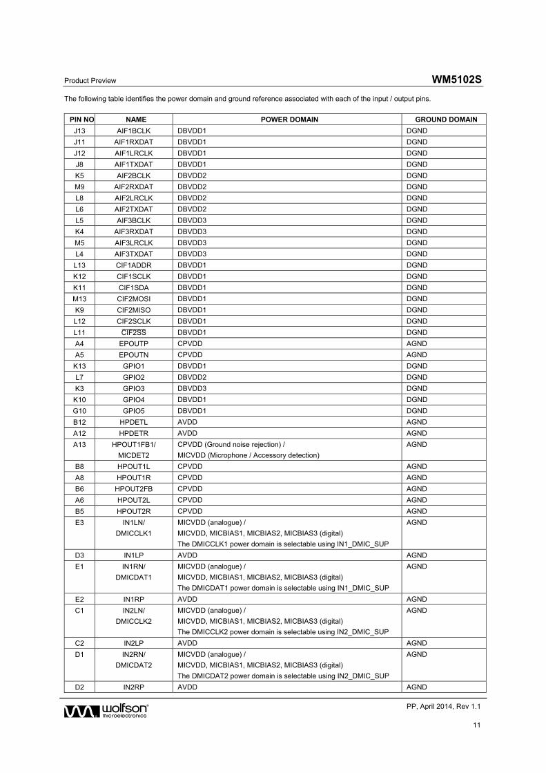
The following table identifies the power domain and ground reference associated with each of the input / output pins.
PIN NO NAME POWER DOMAIN GROUND DOMAIN
J13 AIF1BCLK DBVDD1 DGND
J11 AIF1RXDAT DBVDD1 DGND
J12 AIF1LRCLK DBVDD1 DGND
J8 AIF1TXDAT DBVDD1 DGND
K5 AIF2BCLK DBVDD2 DGND
M9 AIF2RXDAT DBVDD2 DGND
L8 AIF2LRCLK DBVDD2 DGND
L6 AIF2TXDAT DBVDD2 DGND
L5 AIF3BCLK DBVDD3 DGND
K4 AIF3RXDAT DBVDD3 DGND
M5 AIF3LRCLK DBVDD3 DGND
L4 AIF3TXDAT DBVDD3 DGND
L13 CIF1ADDR DBVDD1 DGND
K12 CIF1SCLK DBVDD1 DGND
K11 CIF1SDA DBVDD1 DGND
M13 CIF2MOSI DBVDD1 DGND
K9 CIF2MISO DBVDD1 DGND
L12 CIF2SCLK DBVDD1 DGND
L11 CIF2SS¯¯¯¯¯¯ DBVDD1 DGND
A4 EPOUTP CPVDD AGND
A5 EPOUTN CPVDD AGND
K13 GPIO1 DBVDD1 DGND
L7 GPIO2 DBVDD2 DGND
K3 GPIO3 DBVDD3 DGND
K10 GPIO4 DBVDD1 DGND
G10 GPIO5 DBVDD1 DGND
B12 HPDETL AVDD AGND
A12 HPDETR AVDD AGND
A13 HPOUT1FB1/
MICDET2
CPVDD (Ground noise rejection) /
MICVDD (Microphone / Accessory detection)
AGND
B8 HPOUT1L CPVDD AGND
A8 HPOUT1R CPVDD AGND
B6 HPOUT2FB CPVDD AGND
A6 HPOUT2L CPVDD AGND
B5 HPOUT2R CPVDD AGND
E3 IN1LN/
DMICCLK1
MICVDD (analogue) /
MICVDD, MICBIAS1, MICBIAS2, MICBIAS3 (digital)
The DMICCLK1 power domain is selectable using IN1_DMIC_SUP
AGND
D3 IN1LP AVDD AGND
E1 IN1RN/
DMICDAT1
MICVDD (analogue) /
MICVDD, MICBIAS1, MICBIAS2, MICBIAS3 (digital)
The DMICDAT1 power domain is selectable using IN1_DMIC_SUP
AGND
E2 IN1RP AVDD AGND
C1 IN2LN/
DMICCLK2
MICVDD (analogue) /
MICVDD, MICBIAS1, MICBIAS2, MICBIAS3 (digital)
The DMICCLK2 power domain is selectable using IN2_DMIC_SUP
AGND
C2 IN2LP AVDD AGND
D1 IN2RN/
DMICDAT2
MICVDD (analogue) /
MICVDD, MICBIAS1, MICBIAS2, MICBIAS3 (digital)
The DMICDAT2 power domain is selectable using IN2_DMIC_SUP
AGND
D2 IN2RP AVDD AGND
WM5102S Product Preview
w PP, April 2014, Rev 1.1
12
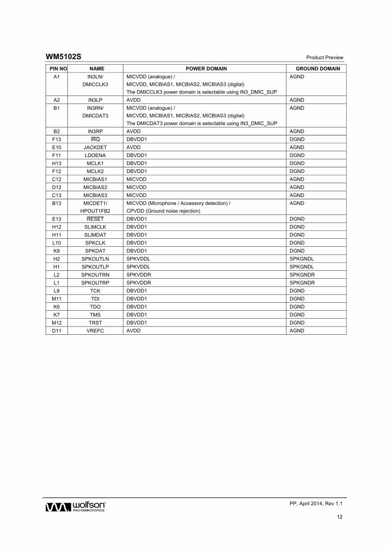
PIN NO NAME POWER DOMAIN GROUND DOMAIN
A1 IN3LN/
DMICCLK3
MICVDD (analogue) /
MICVDD, MICBIAS1, MICBIAS2, MICBIAS3 (digital)
The DMICCLK3 power domain is selectable using IN3_DMIC_SUP
AGND
A2 IN3LP AVDD AGND
B1 IN3RN/
DMICDAT3
MICVDD (analogue) /
MICVDD, MICBIAS1, MICBIAS2, MICBIAS3 (digital)
The DMICDAT3 power domain is selectable using IN3_DMIC_SUP
AGND
B2 IN3RP AVDD AGND
F13 IRQ¯¯¯ DBVDD1 DGND
E10 JACKDET AVDD AGND
F11 LDOENA DBVDD1 DGND
H13 MCLK1 DBVDD1 DGND
F12 MCLK2 DBVDD1 DGND
C12 MICBIAS1 MICVDD AGND
D12 MICBIAS2 MICVDD AGND
C13 MICBIAS3 MICVDD AGND
B13 MICDET1/
HPOUT1FB2
MICVDD (Microphone / Accessory detection) /
CPVDD (Ground noise rejection)
AGND
E13 RESET¯¯¯¯¯¯ DBVDD1 DGND
H12 SLIMCLK DBVDD1 DGND
H11 SLIMDAT DBVDD1 DGND
L10 SPKCLK DBVDD1 DGND
K8 SPKDAT DBVDD1 DGND
H2 SPKOUTLN SPKVDDL SPKGNDL
H1 SPKOUTLP SPKVDDL SPKGNDL
L2 SPKOUTRN SPKVDDR SPKGNDR
L1 SPKOUTRP SPKVDDR SPKGNDR
L9 TCK DBVDD1 DGND
M11 TDI DBVDD1 DGND
K6 TDO DBVDD1 DGND
K7 TMS DBVDD1 DGND
M12 TRST DBVDD1 DGND
D11 VREFC AVDD AGND
Product Preview WM5102S
w PP, April 2014, Rev 1.1
13
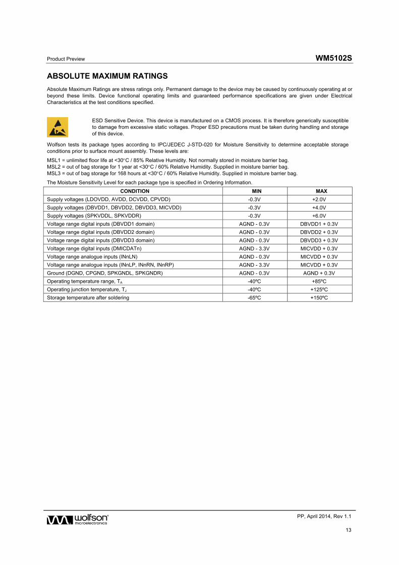
ABSOLUTE MAXIMUM RATINGS
Absolute Maximum Ratings are stress ratings only. Permanent damage to the device may be caused by continuously operating at or beyond these limits. Device functional operating limits and guaranteed performance specifications are given under Electrical Characteristics at the test conditions specified.
ESD Sensitive Device. This device is manufactured on a CMOS process. It is therefore generically susceptible to damage from excessive static voltages. Proper ESD precautions must be taken during handling and storage of this device.
Wolfson tests its package types according to IPC/JEDEC J-STD-020 for Moisture Sensitivity to determine acceptable storage conditions prior to surface mount assembly. These levels are:
MSL1 = unlimited floor life at <30C / 85% Relative Humidity. Not normally stored in moisture barrier bag. MSL2 = out of bag storage for 1 year at <30C / 60% Relative Humidity. Supplied in moisture barrier bag. MSL3 = out of bag storage for 168 hours at <30C / 60% Relative Humidity. Supplied in moisture barrier bag.
The Moisture Sensitivity Level for each package type is specified in Ordering Information.
CONDITION MIN MAX
Supply voltages (LDOVDD, AVDD, DCVDD, CPVDD) -0.3V +2.0V
Supply voltages (DBVDD1, DBVDD2, DBVDD3, MICVDD) -0.3V +4.0V
Supply voltages (SPKVDDL, SPKVDDR) -0.3V +6.0V
Voltage range digital inputs (DBVDD1 domain) AGND - 0.3V DBVDD1 + 0.3V
Voltage range digital inputs (DBVDD2 domain) AGND - 0.3V DBVDD2 + 0.3V
Voltage range digital inputs (DBVDD3 domain) AGND - 0.3V DBVDD3 + 0.3V
Voltage range digital inputs (DMICDATn) AGND - 3.3V MICVDD + 0.3V
Voltage range analogue inputs (INnLN) AGND - 0.3V MICVDD + 0.3V
Voltage range analogue inputs (INnLP, INnRN, INnRP) AGND - 3.3V MICVDD + 0.3V
Ground (DGND, CPGND, SPKGNDL, SPKGNDR) AGND - 0.3V AGND + 0.3V
Operating temperature range, TA -40ºC +85ºC
Operating junction temperature, TJ -40ºC +125ºC
Storage temperature after soldering -65ºC +150ºC
WM5102S Product Preview
w PP, April 2014, Rev 1.1
14
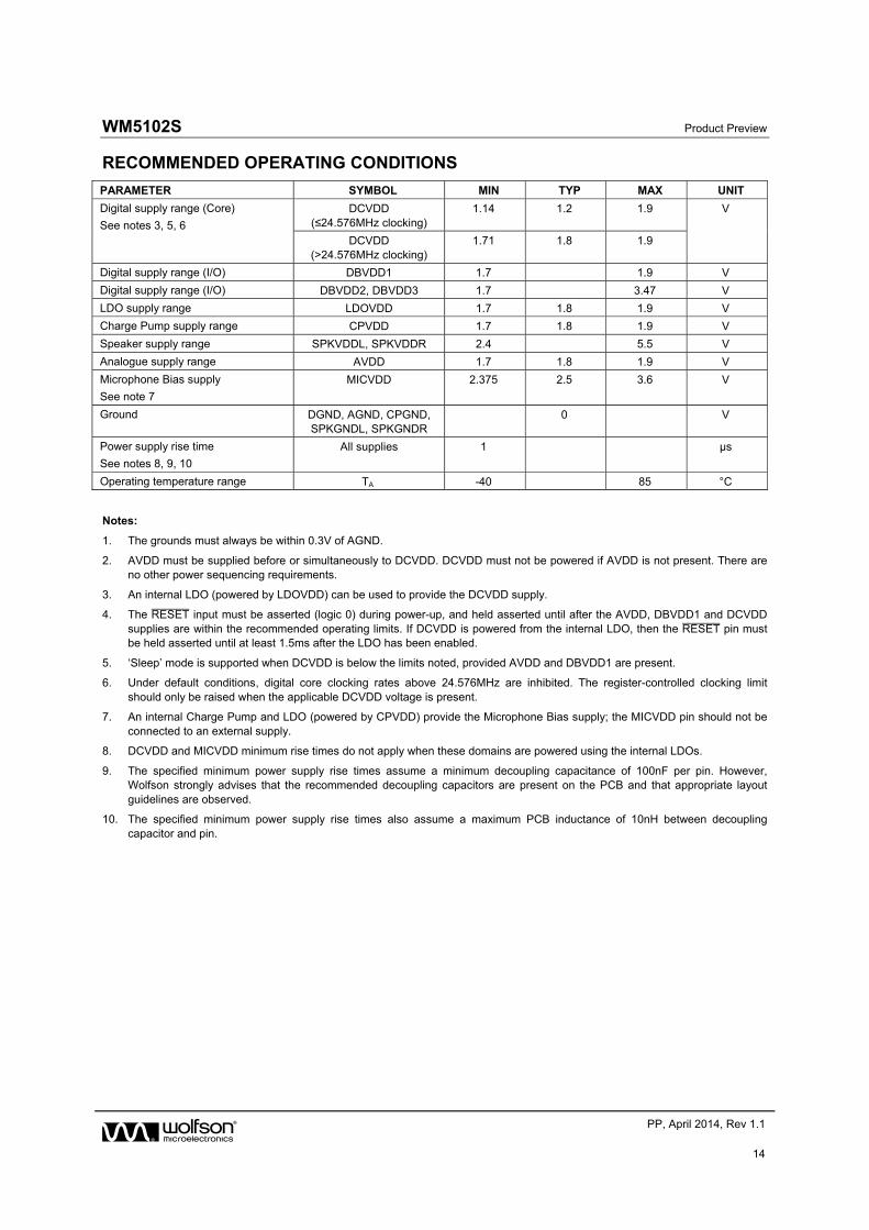
RECOMMENDED OPERATING CONDITIONS
PARAMETER SYMBOL MIN TYP MAX UNIT
Digital supply range (Core)
See notes 3, 5, 6
DCVDD (≤24.576MHz clocking)
1.14 1.2 1.9 V
DCVDD (>24.576MHz clocking)
1.71 1.8 1.9
Digital supply range (I/O) DBVDD1 1.7 1.9 V
Digital supply range (I/O) DBVDD2, DBVDD3 1.7 3.47 V
LDO supply range LDOVDD 1.7 1.8 1.9 V
Charge Pump supply range CPVDD 1.7 1.8 1.9 V
Speaker supply range SPKVDDL, SPKVDDR 2.4 5.5 V
Analogue supply range AVDD 1.7 1.8 1.9 V
Microphone Bias supply
See note 7
MICVDD 2.375 2.5 3.6 V
Ground DGND, AGND, CPGND, SPKGNDL, SPKGNDR
0 V
Power supply rise time
See notes 8, 9, 10
All supplies 1 µs
Operating temperature range TA -40 85 °C
Notes:
1. The grounds must always be within 0.3V of AGND.
2. AVDD must be supplied before or simultaneously to DCVDD. DCVDD must not be powered if AVDD is not present. There are no other power sequencing requirements.
3. An internal LDO (powered by LDOVDD) can be used to provide the DCVDD supply.
4. The RESET¯¯¯¯¯¯ input must be asserted (logic 0) during power-up, and held asserted until after the AVDD, DBVDD1 and DCVDD supplies are within the recommended operating limits. If DCVDD is powered from the internal LDO, then the RESET¯¯¯¯¯¯ pin must be held asserted until at least 1.5ms after the LDO has been enabled.
5. ‘Sleep’ mode is supported when DCVDD is below the limits noted, provided AVDD and DBVDD1 are present.
6. Under default conditions, digital core clocking rates above 24.576MHz are inhibited. The register-controlled clocking limit should only be raised when the applicable DCVDD voltage is present.
7. An internal Charge Pump and LDO (powered by CPVDD) provide the Microphone Bias supply; the MICVDD pin should not be connected to an external supply.
8. DCVDD and MICVDD minimum rise times do not apply when these domains are powered using the internal LDOs.
9. The specified minimum power supply rise times assume a minimum decoupling capacitance of 100nF per pin. However, Wolfson strongly advises that the recommended decoupling capacitors are present on the PCB and that appropriate layout guidelines are observed.
10. The specified minimum power supply rise times also assume a maximum PCB inductance of 10nH between decoupling capacitor and pin.
Product Preview WM5102S
w PP, April 2014, Rev 1.1
15
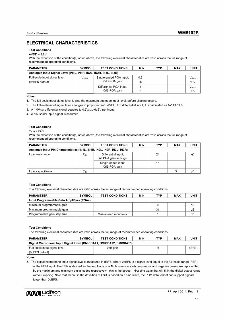
ELECTRICAL CHARACTERISTICS
Test Conditions
AVDD = 1.8V, With the exception of the condition(s) noted above, the following electrical characteristics are valid across the full range of recommended operating conditions.
PARAMETER SYMBOL TEST CONDITIONS MIN TYP MAX UNIT
Analogue Input Signal Level (IN1L, IN1R, IN2L, IN2R, IN3L, IN3R)
Full-scale input signal level
(0dBFS output)
VINFS Single-ended PGA input, 6dB PGA gain
0.5
-6
VRMS
dBV
Differential PGA input, 0dB PGA gain
1
0
VRMS
dBV
Notes:
1. The full-scale input signal level is also the maximum analogue input level, before clipping occurs.
2. The full-scale input signal level changes in proportion with AVDD. For differential input, it is calculated as AVDD / 1.8.
3. A 1.0VRMS differential signal equates to 0.5VRMS/-6dBV per input.
4. A sinusoidal input signal is assumed.
Test Conditions
TA = +25ºC With the exception of the condition(s) noted above, the following electrical characteristics are valid across the full range of recommended operating conditions.
PARAMETER SYMBOL TEST CONDITIONS MIN TYP MAX UNIT
Analogue Input Pin Characteristics (IN1L, IN1R, IN2L, IN2R, IN3L, IN3R)
Input resistance RIN Differential input, All PGA gain settings
24 k
Single-ended input, 0dB PGA gain
16
Input capacitance CIN 5 pF
Test Conditions
The following electrical characteristics are valid across the full range of recommended operating conditions.
PARAMETER SYMBOL TEST CONDITIONS MIN TYP MAX UNIT
Input Programmable Gain Amplifiers (PGAs)
Minimum programmable gain 0 dB
Maximum programmable gain 31 dB
Programmable gain step size Guaranteed monotonic 1 dB
Test Conditions
The following electrical characteristics are valid across the full range of recommended operating conditions.
PARAMETER SYMBOL TEST CONDITIONS MIN TYP MAX UNIT
Digital Microphone Input Signal Level (DMICDAT1, DMICDAT2, DMICDAT3)
Full-scale input signal level
(0dBFS output)
0dB gain -6 dBFS
Notes:
5. The digital microphone input signal level is measured in dBFS, where 0dBFS is a signal level equal to the full-scale range (FSR)
of the PDM input. The FSR is defined as the amplitude of a 1kHz sine wave whose positive and negative peaks are represented
by the maximum and minimum digital codes respectively - this is the largest 1kHz sine wave that will fit in the digital output range
without clipping. Note that, because the definition of FSR is based on a sine wave, the PDM data format can support signals
larger than 0dBFS.
WM5102S Product Preview
w PP, April 2014, Rev 1.1
16
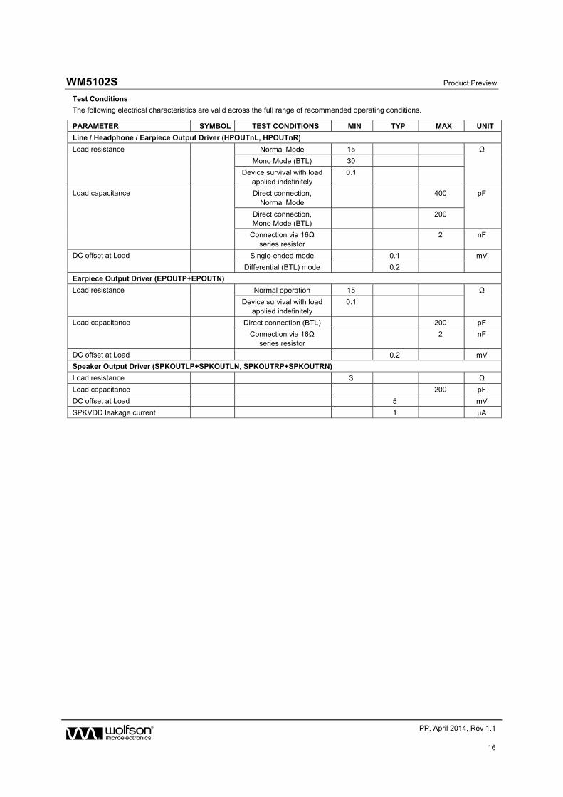
Test Conditions
The following electrical characteristics are valid across the full range of recommended operating conditions.
PARAMETER SYMBOL TEST CONDITIONS MIN TYP MAX UNIT
Line / Headphone / Earpiece Output Driver (HPOUTnL, HPOUTnR)
Load resistance Normal Mode 15 Ω
Mono Mode (BTL) 30
Device survival with load applied indefinitely
0.1
Load capacitance Direct connection, Normal Mode
400 pF
Direct connection, Mono Mode (BTL)
200
Connection via 16Ω series resistor
2 nF
DC offset at Load Single-ended mode 0.1 mV
Differential (BTL) mode 0.2
Earpiece Output Driver (EPOUTP+EPOUTN)
Load resistance Normal operation 15 Ω
Device survival with load applied indefinitely
0.1
Load capacitance Direct connection (BTL) 200 pF
Connection via 16Ω series resistor
2 nF
DC offset at Load 0.2 mV
Speaker Output Driver (SPKOUTLP+SPKOUTLN, SPKOUTRP+SPKOUTRN)
Load resistance 3 Ω
Load capacitance 200 pF
DC offset at Load 5 mV
SPKVDD leakage current 1 µA
Product Preview WM5102S
w PP, April 2014, Rev 1.1
17
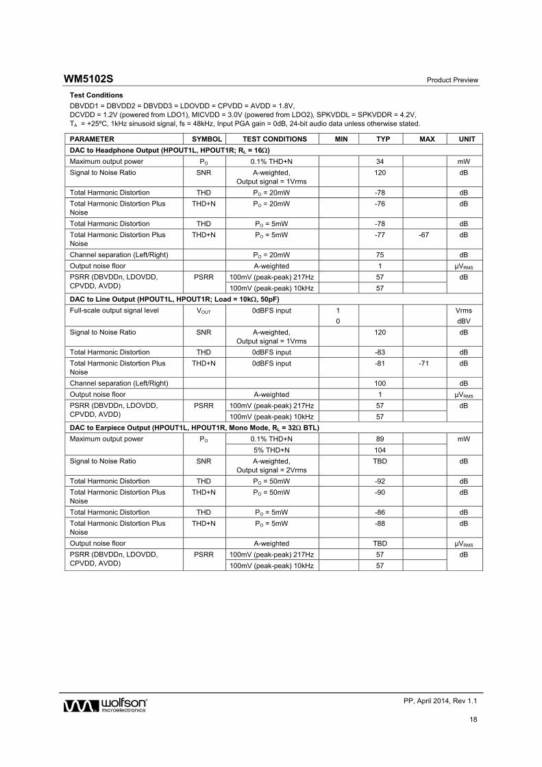
Test Conditions
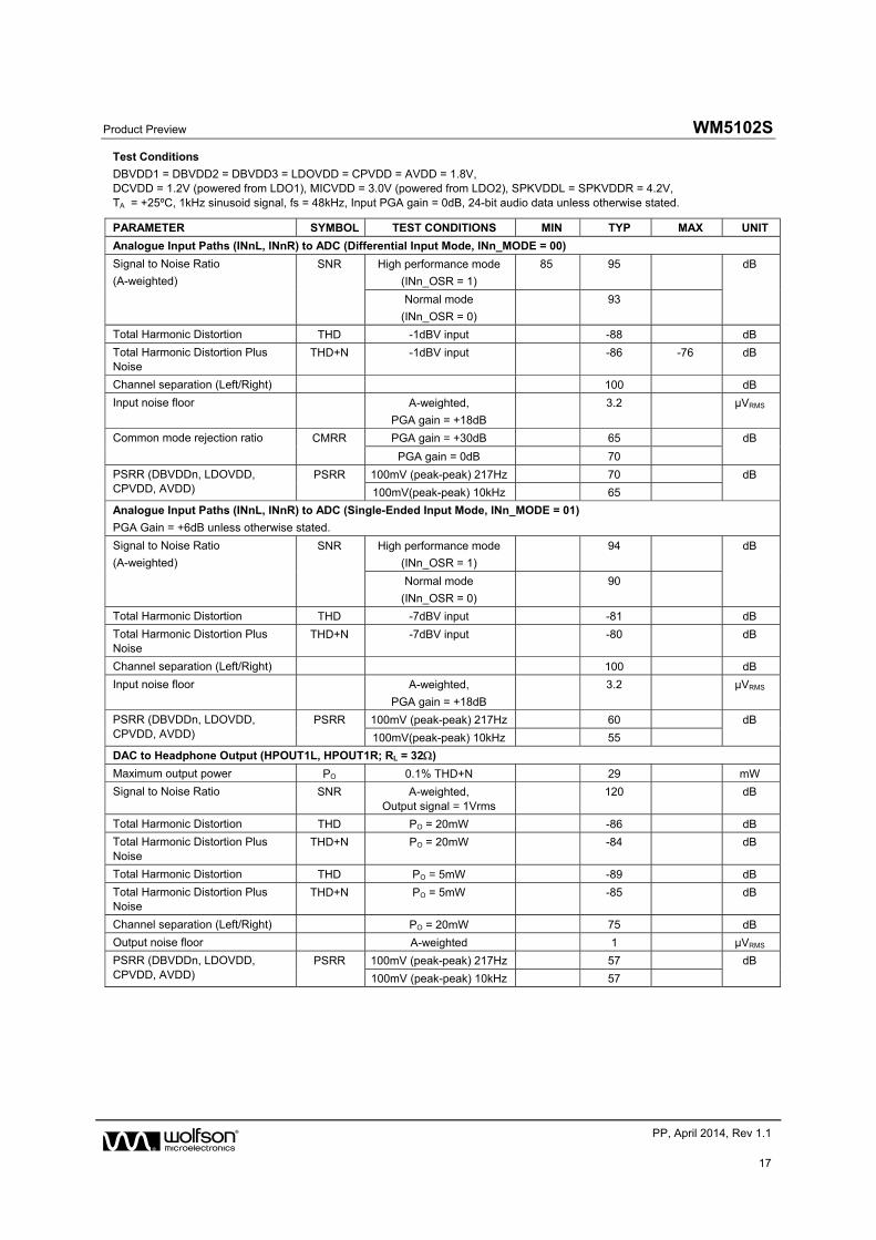
DBVDD1 = DBVDD2 = DBVDD3 = LDOVDD = CPVDD = AVDD = 1.8V, DCVDD = 1.2V (powered from LDO1), MICVDD = 3.0V (powered from LDO2), SPKVDDL = SPKVDDR = 4.2V, TA = +25ºC, 1kHz sinusoid signal, fs = 48kHz, Input PGA gain = 0dB, 24-bit audio data unless otherwise stated.
PARAMETER SYMBOL TEST CONDITIONS MIN TYP MAX UNIT
Analogue Input Paths (INnL, INnR) to ADC (Differential Input Mode, INn_MODE = 00)
Signal to Noise Ratio
(A-weighted)
SNR High performance mode
(INn_OSR = 1)
85 95 dB
Normal mode
(INn_OSR = 0)
93
Total Harmonic Distortion THD -1dBV input -88 dB
Total Harmonic Distortion Plus Noise
THD+N -1dBV input -86 -76 dB
Channel separation (Left/Right) 100 dB
Input noise floor A-weighted,
PGA gain = +18dB
3.2 µVRMS
Common mode rejection ratio CMRR PGA gain = +30dB 65 dB
PGA gain = 0dB 70
PSRR (DBVDDn, LDOVDD, CPVDD, AVDD)
PSRR 100mV (peak-peak) 217Hz 70 dB
100mV(peak-peak) 10kHz 65
Analogue Input Paths (INnL, INnR) to ADC (Single-Ended Input Mode, INn_MODE = 01)
PGA Gain = +6dB unless otherwise stated.
Signal to Noise Ratio
(A-weighted)
SNR High performance mode
(INn_OSR = 1)
94 dB
Normal mode
(INn_OSR = 0)
90
Total Harmonic Distortion THD -7dBV input -81 dB
Total Harmonic Distortion Plus Noise
THD+N -7dBV input -80 dB
Channel separation (Left/Right) 100 dB
Input noise floor A-weighted,
PGA gain = +18dB
3.2 µVRMS
PSRR (DBVDDn, LDOVDD, CPVDD, AVDD)
PSRR 100mV (peak-peak) 217Hz 60 dB
100mV(peak-peak) 10kHz 55
DAC to Headphone Output (HPOUT1L, HPOUT1R; RL = 32)
Maximum output power PO 0.1% THD+N 29 mW
Signal to Noise Ratio SNR A-weighted, Output signal = 1Vrms
120 dB
Total Harmonic Distortion THD PO = 20mW -86 dB
Total Harmonic Distortion Plus Noise
THD+N PO = 20mW -84 dB
Total Harmonic Distortion THD PO = 5mW -89 dB
Total Harmonic Distortion Plus Noise
THD+N PO = 5mW -85 dB
Channel separation (Left/Right) PO = 20mW 75 dB
Output noise floor A-weighted 1 µVRMS
PSRR (DBVDDn, LDOVDD, CPVDD, AVDD)
PSRR 100mV (peak-peak) 217Hz 57 dB
100mV (peak-peak) 10kHz 57
WM5102S Product Preview
w PP, April 2014, Rev 1.1
18
Test Conditions
DBVDD1 = DBVDD2 = DBVDD3 = LDOVDD = CPVDD = AVDD = 1.8V, DCVDD = 1.2V (powered from LDO1), MICVDD = 3.0V (powered from LDO2), SPKVDDL = SPKVDDR = 4.2V, TA = +25ºC, 1kHz sinusoid signal, fs = 48kHz, Input PGA gain = 0dB, 24-bit audio data unless otherwise stated.
PARAMETER SYMBOL TEST CONDITIONS MIN TYP MAX UNIT
DAC to Headphone Output (HPOUT1L, HPOUT1R; RL = 16)
Maximum output power PO 0.1% THD+N 34 mW
Signal to Noise Ratio SNR A-weighted, Output signal = 1Vrms
120 dB
Total Harmonic Distortion THD PO = 20mW -78 dB
Total Harmonic Distortion Plus Noise
THD+N PO = 20mW -76 dB
Total Harmonic Distortion THD PO = 5mW -78 dB
Total Harmonic Distortion Plus Noise
THD+N PO = 5mW -77 -67 dB
Channel separation (Left/Right) PO = 20mW 75 dB
Output noise floor A-weighted 1 µVRMS
PSRR (DBVDDn, LDOVDD, CPVDD, AVDD)
PSRR 100mV (peak-peak) 217Hz 57 dB
100mV (peak-peak) 10kHz 57
DAC to Line Output (HPOUT1L, HPOUT1R; Load = 10k, 50pF)
Full-scale output signal level VOUT 0dBFS input 1
0
Vrms
dBV
Signal to Noise Ratio SNR A-weighted, Output signal = 1Vrms
120 dB
Total Harmonic Distortion THD 0dBFS input -83 dB
Total Harmonic Distortion Plus Noise
THD+N 0dBFS input -81 -71 dB
Channel separation (Left/Right) 100 dB
Output noise floor A-weighted 1 µVRMS
PSRR (DBVDDn, LDOVDD, CPVDD, AVDD)
PSRR 100mV (peak-peak) 217Hz 57 dB
100mV (peak-peak) 10kHz 57
DAC to Earpiece Output (HPOUT1L, HPOUT1R, Mono Mode, RL = 32 BTL)
Maximum output power PO 0.1% THD+N 89 mW
5% THD+N 104
Signal to Noise Ratio SNR A-weighted, Output signal = 2Vrms
TBD dB
Total Harmonic Distortion THD PO = 50mW -92 dB
Total Harmonic Distortion Plus Noise
THD+N PO = 50mW -90 dB
Total Harmonic Distortion THD PO = 5mW -86 dB
Total Harmonic Distortion Plus Noise
THD+N PO = 5mW -88 dB
Output noise floor A-weighted TBD µVRMS
PSRR (DBVDDn, LDOVDD, CPVDD, AVDD)
PSRR 100mV (peak-peak) 217Hz 57 dB
100mV (peak-peak) 10kHz 57
Product Preview WM5102S
w PP, April 2014, Rev 1.1
19
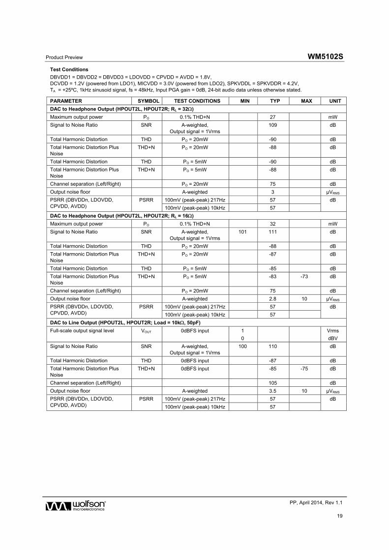
Test Conditions
DBVDD1 = DBVDD2 = DBVDD3 = LDOVDD = CPVDD = AVDD = 1.8V, DCVDD = 1.2V (powered from LDO1), MICVDD = 3.0V (powered from LDO2), SPKVDDL = SPKVDDR = 4.2V, TA = +25ºC, 1kHz sinusoid signal, fs = 48kHz, Input PGA gain = 0dB, 24-bit audio data unless otherwise stated.
PARAMETER SYMBOL TEST CONDITIONS MIN TYP MAX UNIT
DAC to Headphone Output (HPOUT2L, HPOUT2R; RL = 32)
Maximum output power PO 0.1% THD+N 27 mW
Signal to Noise Ratio SNR A-weighted, Output signal = 1Vrms
109 dB
Total Harmonic Distortion THD PO = 20mW -90 dB
Total Harmonic Distortion Plus Noise
THD+N PO = 20mW -88 dB
Total Harmonic Distortion THD PO = 5mW -90 dB
Total Harmonic Distortion Plus Noise
THD+N PO = 5mW -88 dB
Channel separation (Left/Right) PO = 20mW 75 dB
Output noise floor A-weighted 3 µVRMS
PSRR (DBVDDn, LDOVDD, CPVDD, AVDD)
PSRR 100mV (peak-peak) 217Hz 57 dB
100mV (peak-peak) 10kHz 57
DAC to Headphone Output (HPOUT2L, HPOUT2R; RL = 16)
Maximum output power PO 0.1% THD+N 32 mW
Signal to Noise Ratio SNR A-weighted, Output signal = 1Vrms
101 111 dB
Total Harmonic Distortion THD PO = 20mW -88 dB
Total Harmonic Distortion Plus Noise
THD+N PO = 20mW -87 dB
Total Harmonic Distortion THD PO = 5mW -85 dB
Total Harmonic Distortion Plus Noise
THD+N PO = 5mW -83 -73 dB
Channel separation (Left/Right) PO = 20mW 75 dB
Output noise floor A-weighted 2.8 10 µVRMS
PSRR (DBVDDn, LDOVDD, CPVDD, AVDD)
PSRR 100mV (peak-peak) 217Hz 57 dB
100mV (peak-peak) 10kHz 57
DAC to Line Output (HPOUT2L, HPOUT2R; Load = 10k, 50pF)
Full-scale output signal level VOUT 0dBFS input 1
0
Vrms
dBV
Signal to Noise Ratio SNR A-weighted, Output signal = 1Vrms
100 110 dB
Total Harmonic Distortion THD 0dBFS input -87 dB
Total Harmonic Distortion Plus Noise
THD+N 0dBFS input -85 -75 dB
Channel separation (Left/Right) 105 dB
Output noise floor A-weighted 3.5 10 µVRMS
PSRR (DBVDDn, LDOVDD, CPVDD, AVDD)
PSRR 100mV (peak-peak) 217Hz 57 dB
100mV (peak-peak) 10kHz 57
WM5102S Product Preview
w PP, April 2014, Rev 1.1
20
Test Conditions
DBVDD1 = DBVDD2 = DBVDD3 = LDOVDD = CPVDD = AVDD = 1.8V, DCVDD = 1.2V (powered from LDO1), MICVDD = 3.0V (powered from LDO2), SPKVDDL = SPKVDDR = 4.2V, TA = +25ºC, 1kHz sinusoid signal, fs = 48kHz, Input PGA gain = 0dB, 24-bit audio data unless otherwise stated.
PARAMETER SYMBOL TEST CONDITIONS MIN TYP MAX UNIT
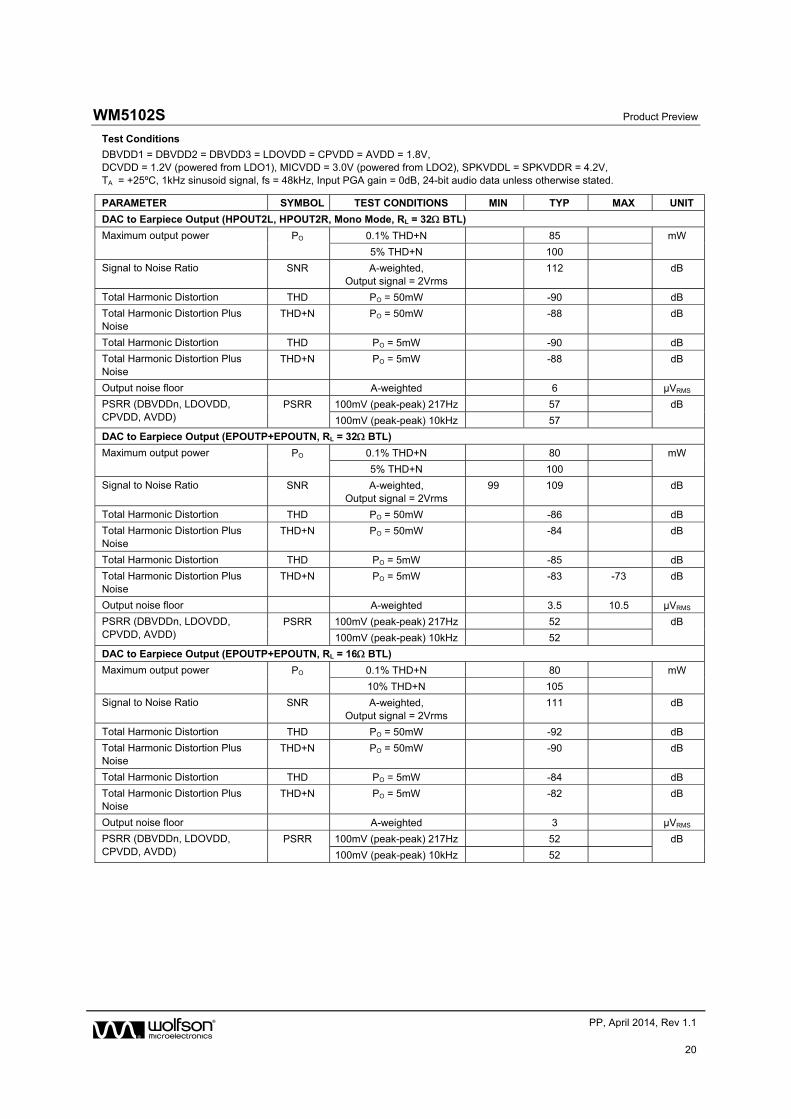
DAC to Earpiece Output (HPOUT2L, HPOUT2R, Mono Mode, RL = 32 BTL)
Maximum output power PO 0.1% THD+N 85 mW
5% THD+N 100
Signal to Noise Ratio SNR A-weighted, Output signal = 2Vrms
112 dB
Total Harmonic Distortion THD PO = 50mW -90 dB
Total Harmonic Distortion Plus Noise
THD+N PO = 50mW -88 dB
Total Harmonic Distortion THD PO = 5mW -90 dB
Total Harmonic Distortion Plus Noise
THD+N PO = 5mW -88 dB
Output noise floor A-weighted 6 µVRMS
PSRR (DBVDDn, LDOVDD, CPVDD, AVDD)
PSRR 100mV (peak-peak) 217Hz 57 dB
100mV (peak-peak) 10kHz 57
DAC to Earpiece Output (EPOUTP+EPOUTN, RL = 32 BTL)
Maximum output power PO 0.1% THD+N 80 mW
5% THD+N 100
Signal to Noise Ratio SNR A-weighted, Output signal = 2Vrms
99 109 dB
Total Harmonic Distortion THD PO = 50mW -86 dB
Total Harmonic Distortion Plus Noise
THD+N PO = 50mW -84 dB
Total Harmonic Distortion THD PO = 5mW -85 dB
Total Harmonic Distortion Plus Noise
THD+N PO = 5mW -83 -73 dB
Output noise floor A-weighted 3.5 10.5 µVRMS
PSRR (DBVDDn, LDOVDD, CPVDD, AVDD)
PSRR 100mV (peak-peak) 217Hz 52 dB
100mV (peak-peak) 10kHz 52
DAC to Earpiece Output (EPOUTP+EPOUTN, RL = 16 BTL)
Maximum output power PO 0.1% THD+N 80 mW
10% THD+N 105
Signal to Noise Ratio SNR A-weighted, Output signal = 2Vrms
111 dB
Total Harmonic Distortion THD PO = 50mW -92 dB
Total Harmonic Distortion Plus Noise
THD+N PO = 50mW -90 dB
Total Harmonic Distortion THD PO = 5mW -84 dB
Total Harmonic Distortion Plus Noise
THD+N PO = 5mW -82 dB
Output noise floor A-weighted 3 µVRMS
PSRR (DBVDDn, LDOVDD, CPVDD, AVDD)
PSRR 100mV (peak-peak) 217Hz 52 dB
100mV (peak-peak) 10kHz 52
Product Preview WM5102S
w PP, April 2014, Rev 1.1
21
Test Conditions
DBVDD1 = DBVDD2 = DBVDD3 = LDOVDD = CPVDD = AVDD = 1.8V, DCVDD = 1.2V (powered from LDO1), MICVDD = 3.0V (powered from LDO2), SPKVDDL = SPKVDDR = 4.2V, TA = +25ºC, 1kHz sinusoid signal, fs = 48kHz, Input PGA gain = 0dB, 24-bit audio data unless otherwise stated.
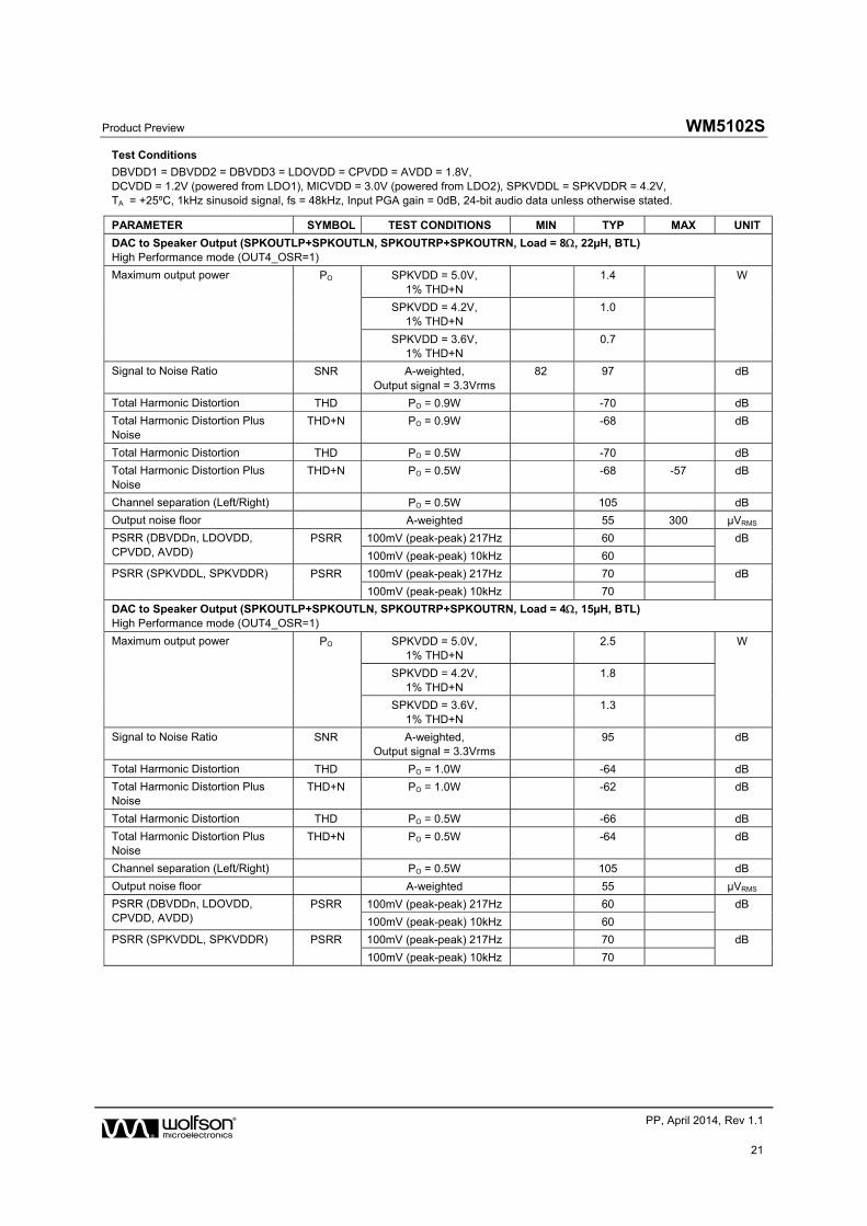
PARAMETER SYMBOL TEST CONDITIONS MIN TYP MAX UNIT
DAC to Speaker Output (SPKOUTLP+SPKOUTLN, SPKOUTRP+SPKOUTRN, Load = 8, 22µH, BTL) High Performance mode (OUT4_OSR=1)
Maximum output power PO SPKVDD = 5.0V, 1% THD+N
1.4 W
SPKVDD = 4.2V, 1% THD+N
1.0
SPKVDD = 3.6V, 1% THD+N
0.7
Signal to Noise Ratio SNR A-weighted, Output signal = 3.3Vrms
82 97 dB
Total Harmonic Distortion THD PO = 0.9W -70 dB
Total Harmonic Distortion Plus Noise
THD+N PO = 0.9W -68 dB
Total Harmonic Distortion THD PO = 0.5W -70 dB
Total Harmonic Distortion Plus Noise
THD+N PO = 0.5W -68 -57 dB
Channel separation (Left/Right) PO = 0.5W 105 dB
Output noise floor A-weighted 55 300 µVRMS
PSRR (DBVDDn, LDOVDD, CPVDD, AVDD)
PSRR 100mV (peak-peak) 217Hz 60 dB
100mV (peak-peak) 10kHz 60
PSRR (SPKVDDL, SPKVDDR) PSRR 100mV (peak-peak) 217Hz 70 dB
100mV (peak-peak) 10kHz 70
DAC to Speaker Output (SPKOUTLP+SPKOUTLN, SPKOUTRP+SPKOUTRN, Load = 4, 15µH, BTL) High Performance mode (OUT4_OSR=1)
Maximum output power PO SPKVDD = 5.0V, 1% THD+N
2.5 W
SPKVDD = 4.2V, 1% THD+N
1.8
SPKVDD = 3.6V, 1% THD+N
1.3
Signal to Noise Ratio SNR A-weighted, Output signal = 3.3Vrms
95 dB
Total Harmonic Distortion THD PO = 1.0W -64 dB
Total Harmonic Distortion Plus Noise
THD+N PO = 1.0W -62 dB
Total Harmonic Distortion THD PO = 0.5W -66 dB
Total Harmonic Distortion Plus Noise
THD+N PO = 0.5W -64 dB
Channel separation (Left/Right) PO = 0.5W 105 dB
Output noise floor A-weighted 55 µVRMS
PSRR (DBVDDn, LDOVDD, CPVDD, AVDD)
PSRR 100mV (peak-peak) 217Hz 60 dB
100mV (peak-peak) 10kHz 60
PSRR (SPKVDDL, SPKVDDR) PSRR 100mV (peak-peak) 217Hz 70 dB
100mV (peak-peak) 10kHz 70
WM5102S Product Preview
w PP, April 2014, Rev 1.1
22
Test Conditions
The following electrical characteristics are valid across the full range of recommended operating conditions.
PARAMETER SYMBOL TEST CONDITIONS MIN TYP MAX UNIT
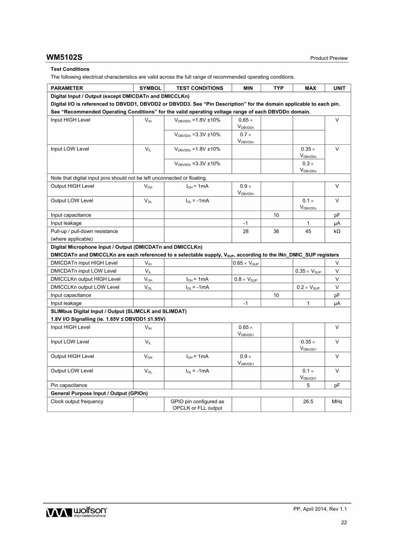
Digital Input / Output (except DMICDATn and DMICCLKn)
Digital I/O is referenced to DBVDD1, DBVDD2 or DBVDD3. See “Pin Description” for the domain applicable to each pin.
See “Recommended Operating Conditions” for the valid operating voltage range of each DBVDDn domain.
Input HIGH Level VIH VDBVDDn =1.8V ±10% 0.65 VDBVDDn
V
VDBVDDn =3.3V ±10% 0.7 VDBVDDn
Input LOW Level VIL VDBVDDn =1.8V ±10% 0.35 VDBVDDn
V
VDBVDDn =3.3V ±10% 0.3 VDBVDDn
Note that digital input pins should not be left unconnected or floating.
Output HIGH Level VOH IOH = 1mA 0.9 VDBVDDn
V
Output LOW Level VOL IOL = -1mA 0.1 VDBVDDn
V
Input capacitance 10 pF
Input leakage -1 1 µA
Pull-up / pull-down resistance
(where applicable)
28 36 45 kΩ
Digital Microphone Input / Output (DMICDATn and DMICCLKn)
DMICDATn and DMICCLKn are each referenced to a selectable supply, VSUP, according to the INn_DMIC_SUP registers
DMICDATn input HIGH Level VIH 0.65 VSUP V
DMICDATn input LOW Level VIL 0.35 VSUP V
DMICCLKn output HIGH Level VOH IOH = 1mA 0.8 VSUP V
DMICCLKn output LOW Level VOL IOL = -1mA 0.2 VSUP V
Input capacitance 10 pF
Input leakage -1 1 µA
SLIMbus Digital Input / Output (SLIMCLK and SLIMDAT)
1.8V I/O Signalling (ie. 1.65V ≤ DBVDD1 ≤1.95V)
Input HIGH Level VIH 0.65 VDBVDD1
V
Input LOW Level VIL 0.35 VDBVDD1
V
Output HIGH Level VOH IOH = 1mA 0.9 VDBVDD1
V
Output LOW Level VOL IOL = -1mA 0.1 VDBVDD1
V
Pin capacitance 5 pF
General Purpose Input / Output (GPIOn)
Clock output frequency GPIO pin configured as OPCLK or FLL output
26.5 MHz
Product Preview WM5102S
w PP, April 2014, Rev 1.1
23
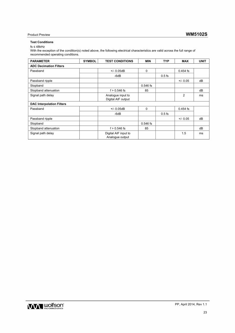
Test Conditions
fs ≤ 48kHz With the exception of the condition(s) noted above, the following electrical characteristics are valid across the full range of recommended operating conditions.
PARAMETER SYMBOL TEST CONDITIONS MIN TYP MAX UNIT
ADC Decimation Filters
Passband +/- 0.05dB 0 0.454 fs
-6dB 0.5 fs
Passband ripple +/- 0.05 dB
Stopband 0.546 fs
Stopband attenuation f > 0.546 fs 85 dB
Signal path delay Analogue input to Digital AIF output
2 ms
DAC Interpolation Filters
Passband +/- 0.05dB 0 0.454 fs
-6dB 0.5 fs
Passband ripple +/- 0.05 dB
Stopband 0.546 fs
Stopband attenuation f > 0.546 fs 85 dB
Signal path delay Digital AIF input to Analogue output
1.5 ms
WM5102S Product Preview
w PP, April 2014, Rev 1.1
24
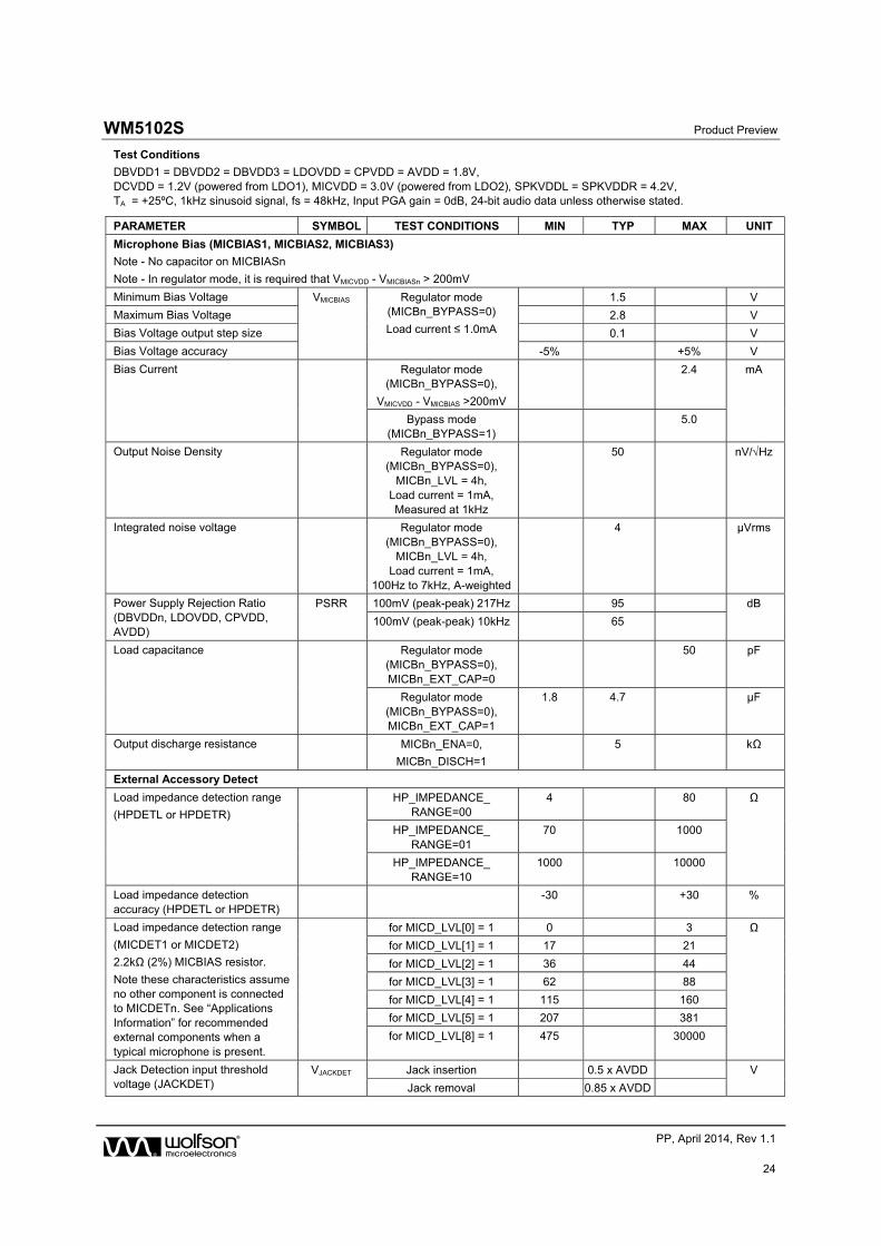
Test Conditions
DBVDD1 = DBVDD2 = DBVDD3 = LDOVDD = CPVDD = AVDD = 1.8V, DCVDD = 1.2V (powered from LDO1), MICVDD = 3.0V (powered from LDO2), SPKVDDL = SPKVDDR = 4.2V, TA = +25ºC, 1kHz sinusoid signal, fs = 48kHz, Input PGA gain = 0dB, 24-bit audio data unless otherwise stated.
PARAMETER SYMBOL TEST CONDITIONS MIN TYP MAX UNIT
Microphone Bias (MICBIAS1, MICBIAS2, MICBIAS3)
Note - No capacitor on MICBIASn
Note - In regulator mode, it is required that VMICVDD - VMICBIASn > 200mV
Minimum Bias Voltage VMICBIAS Regulator mode (MICBn_BYPASS=0)
Load current ≤ 1.0mA
1.5 V
Maximum Bias Voltage 2.8 V
Bias Voltage output step size 0.1 V
Bias Voltage accuracy -5% +5% V
Bias Current Regulator mode (MICBn_BYPASS=0),
VMICVDD - VMICBIAS >200mV
2.4 mA
Bypass mode (MICBn_BYPASS=1)
5.0
Output Noise Density Regulator mode (MICBn_BYPASS=0),
MICBn_LVL = 4h, Load current = 1mA, Measured at 1kHz
50 nV/Hz
Integrated noise voltage Regulator mode (MICBn_BYPASS=0),
MICBn_LVL = 4h, Load current = 1mA,
100Hz to 7kHz, A-weighted
4 µVrms
Power Supply Rejection Ratio (DBVDDn, LDOVDD, CPVDD, AVDD)
PSRR 100mV (peak-peak) 217Hz 95 dB
100mV (peak-peak) 10kHz 65
Load capacitance Regulator mode (MICBn_BYPASS=0), MICBn_EXT_CAP=0
50 pF
Regulator mode (MICBn_BYPASS=0), MICBn_EXT_CAP=1
1.8 4.7 µF
Output discharge resistance MICBn_ENA=0,
MICBn_DISCH=1
5 kΩ
External Accessory Detect
Load impedance detection range
(HPDETL or HPDETR)
HP_IMPEDANCE_ RANGE=00
4 80 Ω
HP_IMPEDANCE_ RANGE=01
70 1000
HP_IMPEDANCE_ RANGE=10
1000 10000
Load impedance detection accuracy (HPDETL or HPDETR)
-30 +30 %
Load impedance detection range
(MICDET1 or MICDET2)
2.2kΩ (2%) MICBIAS resistor.
Note these characteristics assume no other component is connected to MICDETn. See “Applications Information” for recommended external components when a typical microphone is present.
for MICD_LVL[0] = 1 0 3 Ω
for MICD_LVL[1] = 1 17 21
for MICD_LVL[2] = 1 36 44
for MICD_LVL[3] = 1 62 88
for MICD_LVL[4] = 1 115 160
for MICD_LVL[5] = 1 207 381
for MICD_LVL[8] = 1 475 30000
Jack Detection input threshold voltage (JACKDET)
VJACKDET Jack insertion 0.5 x AVDD V
Jack removal 0.85 x AVDD
Product Preview WM5102S
w PP, April 2014, Rev 1.1
25
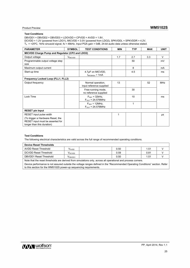
Test Conditions
DBVDD1 = DBVDD2 = DBVDD3 = LDOVDD = CPVDD = AVDD = 1.8V, DCVDD = 1.2V (powered from LDO1), MICVDD = 3.0V (powered from LDO2), SPKVDDL = SPKVDDR = 4.2V, TA = +25ºC, 1kHz sinusoid signal, fs = 48kHz, Input PGA gain = 0dB, 24-bit audio data unless otherwise stated.
PARAMETER SYMBOL TEST CONDITIONS MIN TYP MAX UNIT
MICVDD Charge Pump and Regulator (CP2 and LDO2)
Output voltage VMICVDD 1.7 2.7 3.3 V
Programmable output voltage step size
50 mV
Maximum output current 8 mA
Start-up time 4.7µF on MICVDD, IMICBIASn = 1mA
4.5 ms
Frequency Locked Loop (FLL1, FLL2)
Output frequency Normal operation, input reference supplied
13 52 MHz
Free-running mode, no reference supplied
30
Lock Time FREF = 32kHz, FOUT = 24.576MHz
10 ms
FREF = 12MHz, FOUT = 24.576MHz
1
RESET pin Input
RESET input pulse width
(To trigger a Hardware Reset, the RESET input must be asserted for longer than this duration)
1 µs
Test Conditions
The following electrical characteristics are valid across the full range of recommended operating conditions.
Device Reset Thresholds
AVDD Reset Threshold VAVDD 0.50 1.51 V
DCVDD Reset Threshold VDCVDD 0.59 0.81 V
DBVDD1 Reset Threshold VDBVDD1 0.50 1.51 V
Note that the reset thresholds are derived from simulations only, across all operational and process corners.
Device performance is not assured outside the voltage ranges defined in the “Recommended Operating Conditions” section. Refer to this section for the WM5102S power-up sequencing requirements.
WM5102S Product Preview
w PP, April 2014, Rev 1.1
26
TERMINOLOGY
1. Signal-to-Noise Ratio (dB) – SNR is a measure of the difference in level between the maximum full scale output signal and the output with no input signal applied. (Note that this is measured without any mute function enabled.)
2. Total Harmonic Distortion (dB) – THD is the ratio of the RMS sum of the harmonic distortion products in the specified bandwidth (see note below) relative to the RMS amplitude of the fundamental (ie. test frequency) output.
3. Total Harmonic Distortion plus Noise (dB) – THD+N is the ratio of the RMS sum of the harmonic distortion products plus noise in the specified bandwidth (see note below) relative to the RMS amplitude of the fundamental (ie. test frequency) output.
4. Power Supply Rejection Ratio (dB) - PSRR is the ratio of a specified power supply variation relative to the output signal that results from it. PSRR is measured under quiescent signal path conditions.
5. Common Mode Rejection Ratio (dB) – CMRR is the ratio of a specified input signal (applied to both sides of a differential input), relative to the output signal that results from it.
6. Channel Separation (L/R) (dB) – left-to-right and right-to-left channel separation is the difference in level between the active channel (driven to maximum full scale output) and the measured signal level in the idle channel at the test signal frequency. The active channel is configured and supplied with an appropriate input signal to drive a full scale output, with signal measured at the output of the associated idle channel.
7. Multi-Path Crosstalk (dB) – is the difference in level between the output of the active path and the measured signal level in the idle path at the test signal frequency. The active path is configured and supplied with an appropriate input signal to drive a full scale output, with signal measured at the output of the specified idle path.
8. Mute Attenuation – This is a measure of the difference in level between the full scale output signal and the output with mute applied.
9. All performance measurements are specified with a 20kHz low pass ‘brick-wall’ filter and, where noted, an A-weighted filter. Failure to use these filters will result in higher THD and lower SNR readings than are found in the Electrical Characteristics. The low pass filter removes out of band noise.
Product Preview WM5102S
w PP, April 2014, Rev 1.1
27
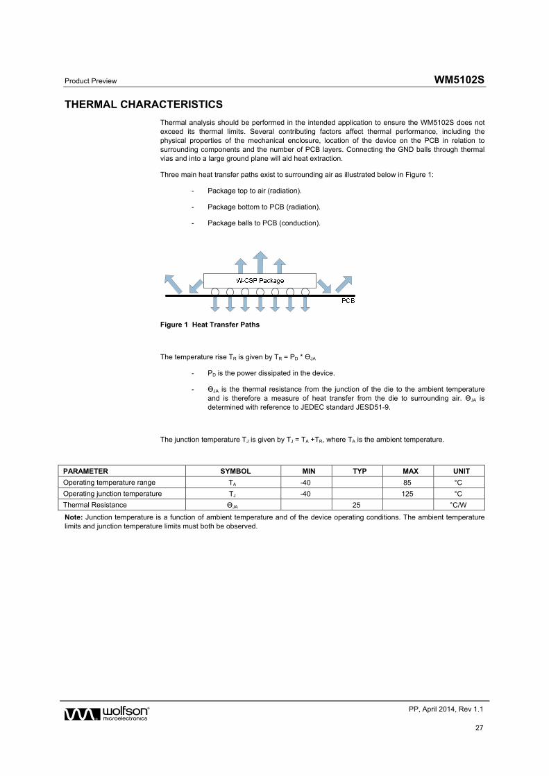
THERMAL CHARACTERISTICS
Thermal analysis should be performed in the intended application to ensure the WM5102S does not exceed its thermal limits. Several contributing factors affect thermal performance, including the physical properties of the mechanical enclosure, location of the device on the PCB in relation to surrounding components and the number of PCB layers. Connecting the GND balls through thermal vias and into a large ground plane will aid heat extraction.
Three main heat transfer paths exist to surrounding air as illustrated below in Figure 1:
- Package top to air (radiation).
- Package bottom to PCB (radiation).
- Package balls to PCB (conduction).
Figure 1 Heat Transfer Paths
The temperature rise TR is given by TR = PD * ӨJA
- PD is the power dissipated in the device.
- ӨJA is the thermal resistance from the junction of the die to the ambient temperature and is therefore a measure of heat transfer from the die to surrounding air. ӨJA is determined with reference to JEDEC standard JESD51-9.
The junction temperature TJ is given by TJ = TA +TR, where TA is the ambient temperature.
PARAMETER SYMBOL MIN TYP MAX UNIT
Operating temperature range TA -40 85 °C
Operating junction temperature TJ -40 125 °C
Thermal Resistance ӨJA 25 °C/W
Note: Junction temperature is a function of ambient temperature and of the device operating conditions. The ambient temperature limits and junction temperature limits must both be observed.
WM5102S Product Preview
w PP, April 2014, Rev 1.1
28
TYPICAL PERFORMANCE
TYPICAL POWER CONSUMPTION
Typical power consumption data is provided below for a number of different operating conditions.
Test Conditions:
DBVDD1 = DBVDD2 = DBVDD3 = LDOVDD = CPVDD = AVDD = 1.8V,
SPKVDDL = SPKVDDR = 4.2V,
DCVDD = 1.2V (powered from LDO1), MICVDD = 3.0V (powered from LDO2), TA = +25ºC
OPERATING MODE TEST CONDITIONS SUPPLY CURRENT
(1.8V)
SUPPLY CURRENT
(4.2V)
TOTAL POWER
Music Playback to Headphone
AIF1 to DAC to HPOUT1 (stereo)
fs=48kHz, 24-bit I2S, Slave mode
Load = 32
Quiescent TBD TBD TBD
1kHz sine wave, PO=10mW TBD TBD TBD
Music Playback to Line Output
AIF1 to DAC to HPOUT2 (stereo)
fs=48kHz, 24-bit I2S, Slave mode
Load = 10k, 50pF
Quiescent 4.4mA 0.0mA 7.9mW
Music Playback to Earpiece
AIF1 to DAC to EPOUT (mono)
fs=48kHz, 24-bit I2S, Slave mode
Load = 32, 22µH, BTL
Quiescent 5.3mA 0.0mA 9.5mW
1kHz sine wave, PO=30mW 59.7mA 0.0mA 107.5mW
Music Playback to Speaker
AIF1 to DAC to SPKOUT (stereo)
fs=48kHz, 24-bit I2S, Slave mode
Load = 8, 22µH, BTL
Quiescent 5.5mA 5.8mA 34.3mW
1kHz sine wave, PO=700mW 5.6mA 380mA 1606mW
Full Duplex Voice Call
Analogue Mic to ADC to AIF1 (out)
AIF (in) to DAC to EPOUT (mono)
fs=8kHz, 16-bit I2S, Slave mode
Low Power mode (INn_OSR=00)
Load = 32, 22µH, BTL
Quiescent 6.7mA 0.0mA 12mW
Stereo Line Record
Analogue Line to ADC to AIF1
fs=48kHz, 24-bit I2S, Slave mode
Low Power mode (INn_OSR=00)
1kHz sine wave, -1dBFS out 4.2mA 0.0mA 7.6mW
Sleep Mode
Accessory detect enabled (JD1_ENA=1) 0.015mA 0.0mA 0.03mW
Product Preview WM5102S
w PP, April 2014, Rev 1.1
29
TYPICAL SIGNAL LATENCY
OPERATING MODE TEST CONDITIONS LATENCY
INPUT OUTPUT DIGITAL CORE
AIF to DAC Stereo Path
Digital input (AIFn) to analogue output (EPOUT).
Signal is routed via the digital core ASRC function in the asynchronous test cases only.
fs = 48kHz fs = 48kHz Synchronous 352µs
fs = 44.1kHz fs = 44.1kHz Synchronous 362µs
fs = 16kHz fs = 16kHz Synchronous 711µs
fs = 8kHz fs = 8kHz Synchronous 3580µs
fs = 8kHz fs = 44.1kHz Asynchronous 3750µs
fs = 16kHz fs = 44.1kHz Asynchronous 848µs
ADC to AIF Stereo Path
Analogue input (INn) to digital output (AIFn).
Digital core High Pass filter included in signal path.
Signal is routed via the digital core ASRC function in the asynchronous test cases only.
fs = 48kHz fs = 48kHz Synchronous 268µs
fs = 44.1kHz fs = 44.1kHz Synchronous 292µs
fs = 16kHz fs = 16kHz Synchronous 894µs
fs = 8kHz fs = 8kHz Synchronous 1730µs
fs = 44.1kHz fs = 8kHz Asynchronous 880µs
fs = 44.1kHz fs = 16kHz Asynchronous 530µs
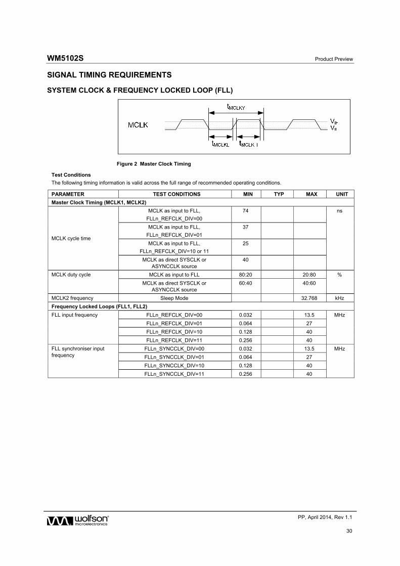
WM5102S Product Preview
w PP, April 2014, Rev 1.1
30
SIGNAL TIMING REQUIREMENTS
SYSTEM CLOCK & FREQUENCY LOCKED LOOP (FLL)
Figure 2 Master Clock Timing
Test Conditions
The following timing information is valid across the full range of recommended operating conditions.
PARAMETER TEST CONDITIONS MIN TYP MAX UNIT
Master Clock Timing (MCLK1, MCLK2)
MCLK cycle time
MCLK as input to FLL,
FLLn_REFCLK_DIV=00
74 ns
MCLK as input to FLL,
FLLn_REFCLK_DIV=01
37
MCLK as input to FLL,
FLLn_REFCLK_DIV=10 or 11
25
MCLK as direct SYSCLK or ASYNCCLK source
40
MCLK duty cycle MCLK as input to FLL 80:20 20:80 %
MCLK as direct SYSCLK or ASYNCCLK source
60:40 40:60
MCLK2 frequency Sleep Mode 32.768 kHz
Frequency Locked Loops (FLL1, FLL2)
FLL input frequency FLLn_REFCLK_DIV=00 0.032 13.5 MHz
FLLn_REFCLK_DIV=01 0.064 27
FLLn_REFCLK_DIV=10 0.128 40
FLLn_REFCLK_DIV=11 0.256 40
FLL synchroniser input frequency
FLLn_SYNCCLK_DIV=00 0.032 13.5 MHz
FLLn_SYNCCLK_DIV=01 0.064 27
FLLn_SYNCCLK_DIV=10 0.128 40
FLLn_SYNCCLK_DIV=11 0.256 40
Product Preview WM5102S
w PP, April 2014, Rev 1.1
31
Test Conditions
The following timing information is valid across the full range of recommended operating conditions.
PARAMETER TEST CONDITIONS MIN TYP MAX UNIT
Internal Clocking
SYSCLK frequency SYSCLK_FREQ=000, SYSCLK_FRAC=0 -1% 6.144 +1% MHz
SYSCLK_FREQ=000, SYSCLK_FRAC=1 -1% 5.6448 +1%
SYSCLK_FREQ=001, SYSCLK_FRAC=0 -1% 12.288 +1%
SYSCLK_FREQ=001, SYSCLK_FRAC=1 -1% 11.2896 +1%
SYSCLK_FREQ=010, SYSCLK_FRAC=0 -1% 24.576 +1%
SYSCLK_FREQ=010, SYSCLK_FRAC=1 -1% 22.5792 +1%
SYSCLK_FREQ=011, SYSCLK_FRAC=0 -1% 49.152 +1%
SYSCLK_FREQ=011, SYSCLK_FRAC=1 -1% 45.1584 +1%
ASYNCCLK frequency ASYNC_CLK_FREQ=000 -1% 6.144 +1% MHz
-1% 5.6448 +1%
ASYNC_CLK_FREQ=001 -1% 12.288 +1%
-1% 11.2896 +1%
ASYNC_CLK_FREQ=010 -1% 24.576 +1%
-1% 22.5792 +1%
ASYNC_CLK_FREQ=011 -1% 49.152 +1%
-1% 45.1584 +1%
Note:
When MCLK1 or MCLK2 is selected as a source for SYSCLK or ASYNCCLK (either directly or via one of the FLLs), the frequency
must be within 1% of the applicable SYSCLK_FREQ or ASYNCCLK_FREQ register setting.
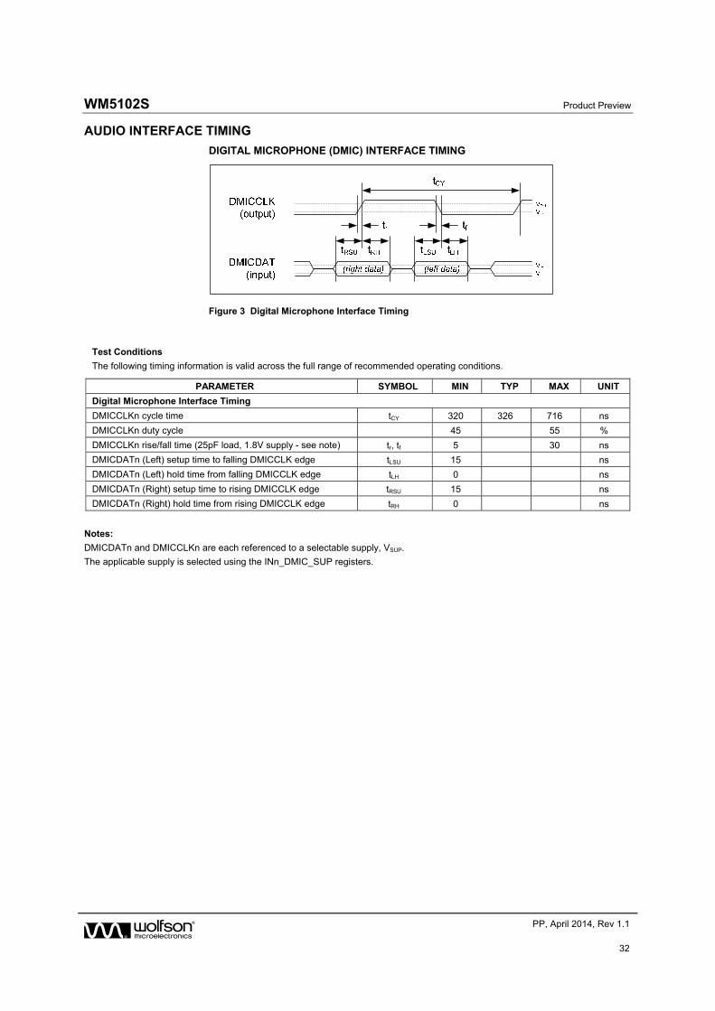
WM5102S Product Preview
w PP, April 2014, Rev 1.1
32
AUDIO INTERFACE TIMING
DIGITAL MICROPHONE (DMIC) INTERFACE TIMING
Figure 3 Digital Microphone Interface Timing
Test Conditions
The following timing information is valid across the full range of recommended operating conditions.
PARAMETER SYMBOL MIN TYP MAX UNIT
Digital Microphone Interface Timing
DMICCLKn cycle time tCY 320 326 716 ns
DMICCLKn duty cycle 45 55 %
DMICCLKn rise/fall time (25pF load, 1.8V supply - see note) tr, tf 5 30 ns
DMICDATn (Left) setup time to falling DMICCLK edge tLSU 15 ns
DMICDATn (Left) hold time from falling DMICCLK edge tLH 0 ns
DMICDATn (Right) setup time to rising DMICCLK edge tRSU 15 ns
DMICDATn (Right) hold time from rising DMICCLK edge tRH 0 ns
Notes:
DMICDATn and DMICCLKn are each referenced to a selectable supply, VSUP.
The applicable supply is selected using the INn_DMIC_SUP registers.
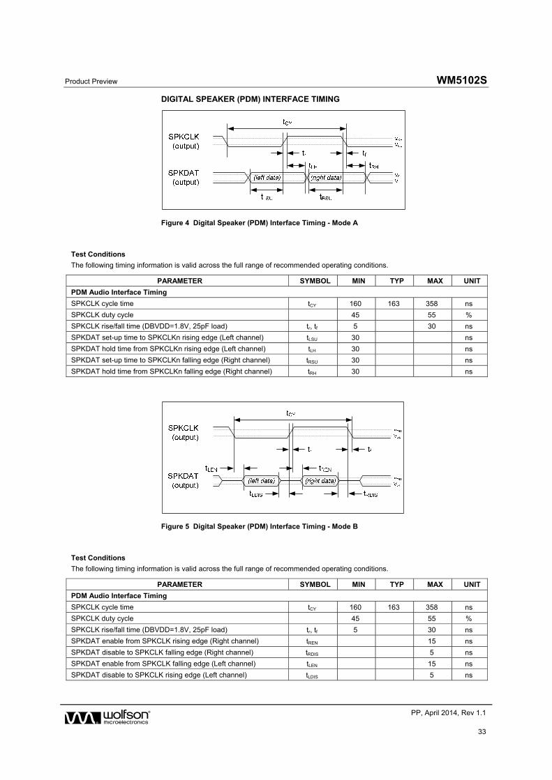
Product Preview WM5102S
w PP, April 2014, Rev 1.1
33
DIGITAL SPEAKER (PDM) INTERFACE TIMING
Figure 4 Digital Speaker (PDM) Interface Timing - Mode A
Test Conditions
The following timing information is valid across the full range of recommended operating conditions.
PARAMETER SYMBOL MIN TYP MAX UNIT
PDM Audio Interface Timing
SPKCLK cycle time tCY 160 163 358 ns
SPKCLK duty cycle 45 55 %
SPKCLK rise/fall time (DBVDD=1.8V, 25pF load) tr, tf 5 30 ns
SPKDAT set-up time to SPKCLKn rising edge (Left channel) tLSU 30 ns
SPKDAT hold time from SPKCLKn rising edge (Left channel) tLH 30 ns
SPKDAT set-up time to SPKCLKn falling edge (Right channel) tRSU 30 ns
SPKDAT hold time from SPKCLKn falling edge (Right channel) tRH 30 ns
Figure 5 Digital Speaker (PDM) Interface Timing - Mode B
Test Conditions
The following timing information is valid across the full range of recommended operating conditions.
PARAMETER SYMBOL MIN TYP MAX UNIT
PDM Audio Interface Timing
SPKCLK cycle time tCY 160 163 358 ns
SPKCLK duty cycle 45 55 %
SPKCLK rise/fall time (DBVDD=1.8V, 25pF load) tr, tf 5 30 ns
SPKDAT enable from SPKCLK rising edge (Right channel) tREN 15 ns
SPKDAT disable to SPKCLK falling edge (Right channel) tRDIS 5 ns
SPKDAT enable from SPKCLK falling edge (Left channel) tLEN 15 ns
SPKDAT disable to SPKCLK rising edge (Left channel) tLDIS 5 ns
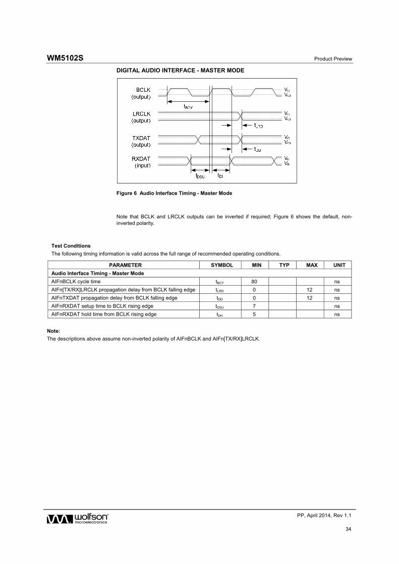
WM5102S Product Preview
w PP, April 2014, Rev 1.1
34
DIGITAL AUDIO INTERFACE - MASTER MODE
Figure 6 Audio Interface Timing - Master Mode
Note that BCLK and LRCLK outputs can be inverted if required; Figure 6 shows the default, non-inverted polarity.
Test Conditions
The following timing information is valid across the full range of recommended operating conditions.
PARAMETER SYMBOL MIN TYP MAX UNIT
Audio Interface Timing - Master Mode
AIFnBCLK cycle time tBCY 80 ns
AIFn[TX/RX]LRCLK propagation delay from BCLK falling edge tLRD 0 12 ns
AIFnTXDAT propagation delay from BCLK falling edge tDD 0 12 ns
AIFnRXDAT setup time to BCLK rising edge tDSU 7 ns
AIFnRXDAT hold time from BCLK rising edge tDH 5 ns
Note:
The descriptions above assume non-inverted polarity of AIFnBCLK and AIFn[TX/RX]LRCLK.
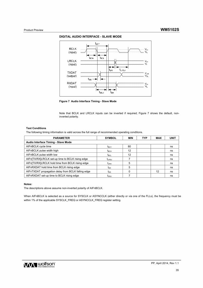
Product Preview WM5102S
w PP, April 2014, Rev 1.1
35
DIGITAL AUDIO INTERFACE - SLAVE MODE
Figure 7 Audio Interface Timing - Slave Mode
Note that BCLK and LRCLK inputs can be inverted if required; Figure 7 shows the default, non-inverted polarity.
Test Conditions
The following timing information is valid across the full range of recommended operating conditions.
PARAMETER SYMBOL MIN TYP MAX UNIT
Audio Interface Timing - Slave Mode
AIFnBCLK cycle time tBCY 80 ns
AIFnBCLK pulse width high tBCH 12 ns
AIFnBCLK pulse width low tBCL 12 ns
AIFn[TX/RX]LRCLK set-up time to BCLK rising edge tLRSU 7 ns
AIFn[TX/RX]LRCLK hold time from BCLK rising edge tLRH 5 ns
AIFnRXDAT hold time from BCLK rising edge tDH 5 ns
AIFnTXDAT propagation delay from BCLK falling edge tDD 0 12 ns
AIFnRXDAT set-up time to BCLK rising edge tDSU 7 ns
Notes:
The descriptions above assume non-inverted polarity of AIFnBCLK.
When AIFnBCLK is selected as a source for SYSCLK or ASYNCCLK (either directly or via one of the FLLs), the frequency must be
within 1% of the applicable SYSCLK_FREQ or ASYNCCLK_FREQ register setting.
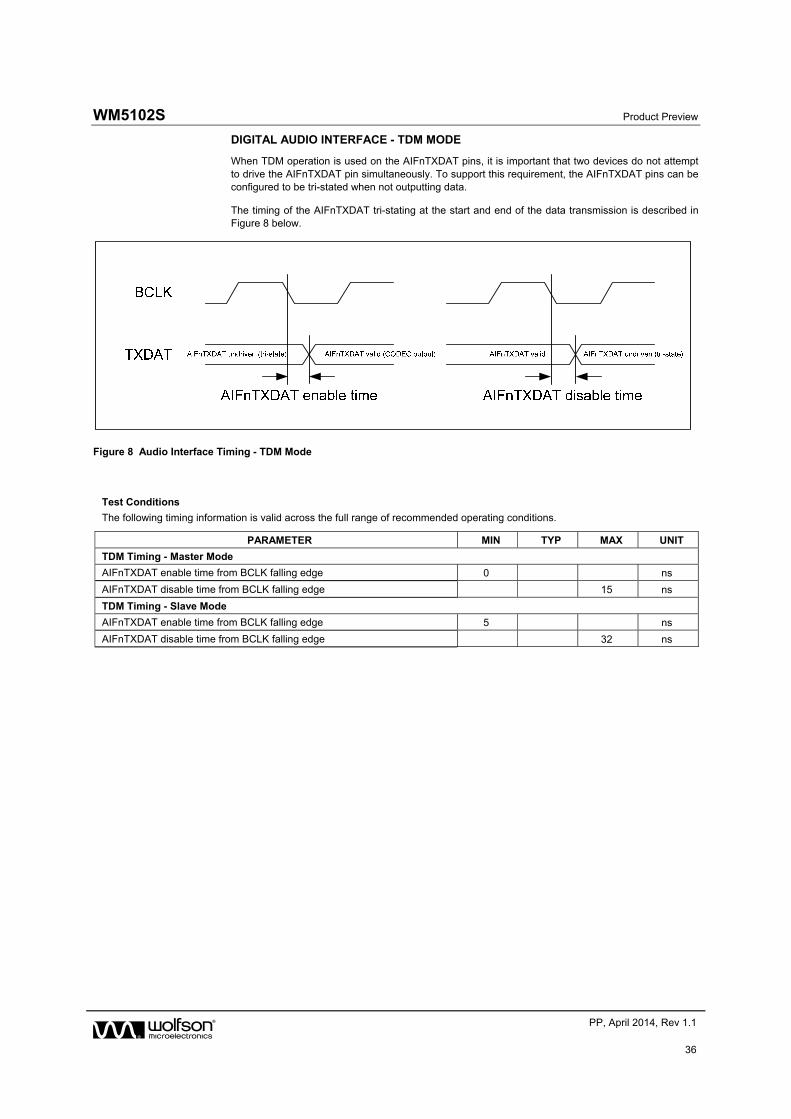
WM5102S Product Preview
w PP, April 2014, Rev 1.1
36
DIGITAL AUDIO INTERFACE - TDM MODE
When TDM operation is used on the AIFnTXDAT pins, it is important that two devices do not attempt to drive the AIFnTXDAT pin simultaneously. To support this requirement, the AIFnTXDAT pins can be configured to be tri-stated when not outputting data.
The timing of the AIFnTXDAT tri-stating at the start and end of the data transmission is described in Figure 8 below.
Figure 8 Audio Interface Timing - TDM Mode
Test Conditions
The following timing information is valid across the full range of recommended operating conditions.
PARAMETER MIN TYP MAX UNIT
TDM Timing - Master Mode
AIFnTXDAT enable time from BCLK falling edge 0 ns
AIFnTXDAT disable time from BCLK falling edge 15 ns
TDM Timing - Slave Mode
AIFnTXDAT enable time from BCLK falling edge 5 ns
AIFnTXDAT disable time from BCLK falling edge 32 ns
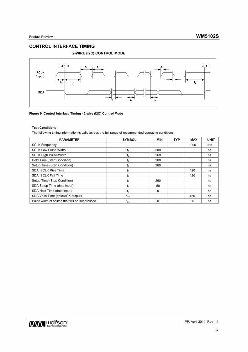
Product Preview WM5102S
w PP, April 2014, Rev 1.1
37
CONTROL INTERFACE TIMING
2-WIRE (I2C) CONTROL MODE
Figure 9 Control Interface Timing - 2-wire (I2C) Control Mode
Test Conditions
The following timing information is valid across the full range of recommended operating conditions.
PARAMETER SYMBOL MIN TYP MAX UNIT
SCLK Frequency 1000 kHz
SCLK Low Pulse-Width t1 500 ns
SCLK High Pulse-Width t2 260 ns
Hold Time (Start Condition) t3 260 ns
Setup Time (Start Condition) t4 260 ns
SDA, SCLK Rise Time t6 120 ns
SDA, SCLK Fall Time t7 120 ns
Setup Time (Stop Condition) t8 260 ns
SDA Setup Time (data input) t5 50 ns
SDA Hold Time (data input) t9 0 ns
SDA Valid Time (data/ACK output) t10 450 ns
Pulse width of spikes that will be suppressed tps 0 50 ns
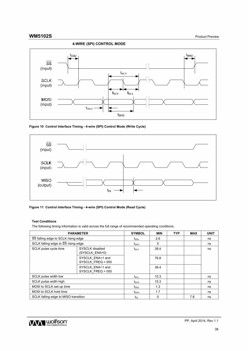
WM5102S Product Preview
w PP, April 2014, Rev 1.1
38
4-WIRE (SPI) CONTROL MODE
Figure 10 Control Interface Timing - 4-wire (SPI) Control Mode (Write Cycle)
Figure 11 Control Interface Timing - 4-wire (SPI) Control Mode (Read Cycle)
Test Conditions
The following timing information is valid across the full range of recommended operating conditions.
PARAMETER SYMBOL MIN TYP MAX UNIT
SS¯¯ falling edge to SCLK rising edge tSSU 2.6 ns
SCLK falling edge to SS¯¯ rising edge tSHO 0 ns
SCLK pulse cycle time SYSCLK disabled (SYSCLK_ENA=0)
tSCY 38.4 ns
SYSCLK_ENA=1 and SYSCLK_FREQ = 000
76.8
SYSCLK_ENA=1 and SYSCLK_FREQ > 000
38.4
SCLK pulse width low tSCL 15.3 ns
SCLK pulse width high tSCH 15.3 ns
MOSI to SCLK set-up time tDSU 1.3 ns
MOSI to SCLK hold time tDHO 1.7 ns
SCLK falling edge to MISO transition tDL 0 7.8 ns
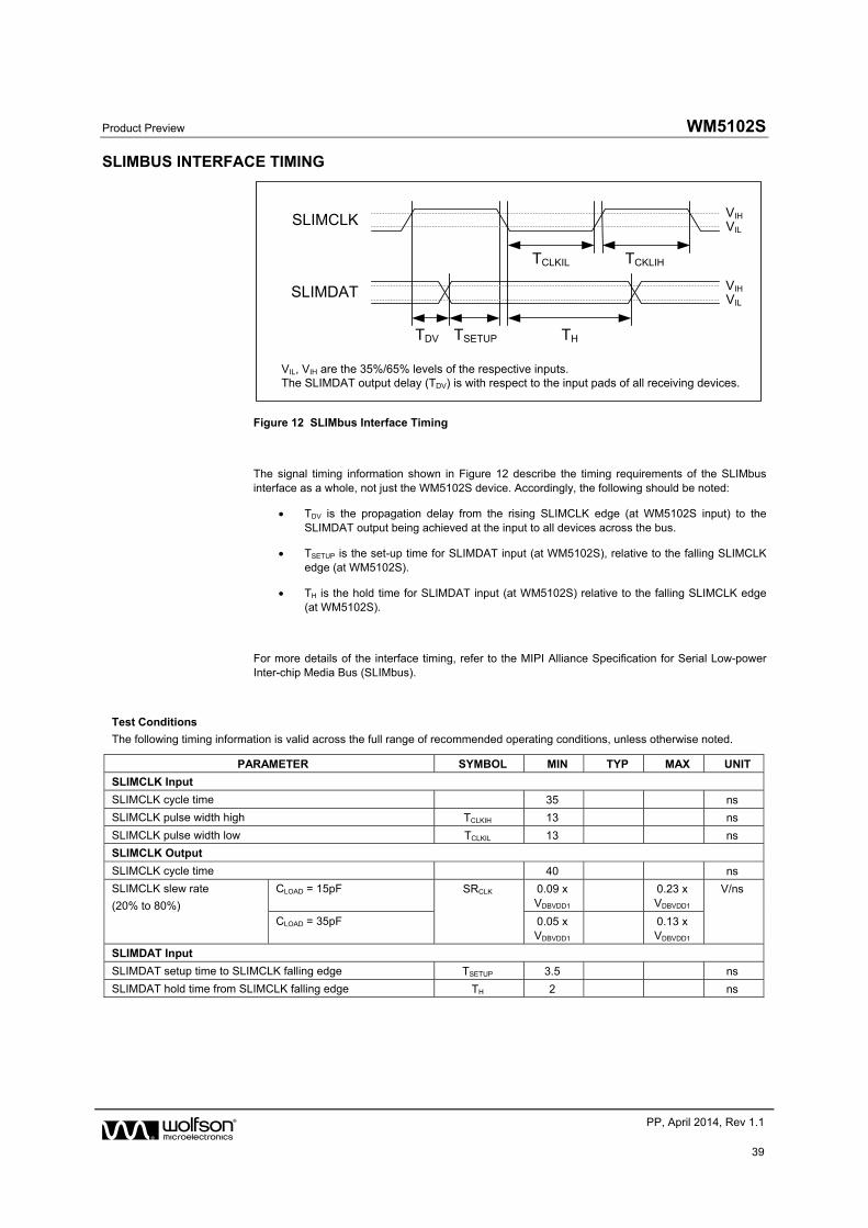
Product Preview WM5102S
w PP, April 2014, Rev 1.1
39
SLIMBUS INTERFACE TIMING
SLIMDAT
TDV
TCLKIL TCKLIH
VIH
VIL
TSETUP TH
VIH
VILSLIMCLK
VIL, VIH are the 35%/65% levels of the respective inputs.The SLIMDAT output delay (TDV) is with respect to the input pads of all receiving devices.
Figure 12 SLIMbus Interface Timing
The signal timing information shown in Figure 12 describe the timing requirements of the SLIMbus interface as a whole, not just the WM5102S device. Accordingly, the following should be noted:
TDV is the propagation delay from the rising SLIMCLK edge (at WM5102S input) to the SLIMDAT output being achieved at the input to all devices across the bus.
TSETUP is the set-up time for SLIMDAT input (at WM5102S), relative to the falling SLIMCLK edge (at WM5102S).
TH is the hold time for SLIMDAT input (at WM5102S) relative to the falling SLIMCLK edge (at WM5102S).
For more details of the interface timing, refer to the MIPI Alliance Specification for Serial Low-power Inter-chip Media Bus (SLIMbus).
Test Conditions
The following timing information is valid across the full range of recommended operating conditions, unless otherwise noted.
PARAMETER SYMBOL MIN TYP MAX UNIT
SLIMCLK Input
SLIMCLK cycle time 35 ns
SLIMCLK pulse width high TCLKIH 13 ns
SLIMCLK pulse width low TCLKIL 13 ns
SLIMCLK Output
SLIMCLK cycle time 40 ns
SLIMCLK slew rate
(20% to 80%)
CLOAD = 15pF SRCLK 0.09 x VDBVDD1
0.23 x VDBVDD1
V/ns
CLOAD = 35pF 0.05 x VDBVDD1
0.13 x VDBVDD1
SLIMDAT Input
SLIMDAT setup time to SLIMCLK falling edge TSETUP 3.5 ns
SLIMDAT hold time from SLIMCLK falling edge TH 2 ns
WM5102S Product Preview
w PP, April 2014, Rev 1.1
40
Test Conditions
The following timing information is valid across the full range of recommended operating conditions, unless otherwise noted.
PARAMETER SYMBOL MIN TYP MAX UNIT
SLIMDAT Output
SLIMDAT time for data output valid (wrt SLIMCLK rising edge)
CLOAD = 15pF, VDBVDD1 = 1.62V
TDV 6.7 8.6 ns
CLOAD = 35pF, VDBVDD1 = 1.62V
9.8 12.5
SLIMDAT slew rate
(20% to 80%)
CLOAD = 15pF SRDATA 0.54 x VDBVDD1
V/ns
CLOAD = 35pF 0.34 x VDBVDD1
Other Parameters
Driver disable time TDD 6 ns
Bus holder output impedance 0.1 x VDBVDD1 < V < 0.9 x VDBVDD1
RDATAS 18 50 kΩ
Product Preview WM5102S
w PP, April 2014, Rev 1.1
41
DEVICE DESCRIPTION
INTRODUCTION
The WM5102S is a highly integrated low-power audio hub CODEC for mobile telephony and portable devices. It provides flexible, high-performance audio interfacing for handheld devices in a small and cost-effective package. A powerful DSP engine is incorporated, offering audiophile quality 24-bit DAC playback at sample rates up to 192kHz. The Master Hi-Fi software, together with other integrated audio processing features, offers a superior listening experience for multimedia phones and smartphones.
The WM5102S digital core provides an extensive capability for signal processing algorithms, including Wolfson’s Master Hi-Fi filters, Enhanced DRE processing (eDRE), side-tone and other programmable filters. Parametric equalisation (EQ) and dynamic range control (DRC) are also supported. Highly flexible digital mixing, including stereo full-duplex asynchronous sample rate conversion, provides use-case flexibility across a broad range of system architectures. A signal generator for controlling haptics vibe actuators is included.
The WM5102S provides multiple digital audio interfaces, including SLIMbus, in order to provide independent and fully asynchronous connections to different processors (eg. application processor, baseband processor and wireless transceiver).
A flexible clocking arrangement supports a wide variety of external clock references, including clocking derived from the digital audio interface. Two integrated Frequency Locked Loop (FLL) circuits provide additional flexibility.
Unused circuitry can be disabled under software control, in order to save power; low leakage currents enable extended standby/off time in portable battery-powered applications. Configurable ‘Wake-Up’ actions can be associated with the low-power standby (Sleep) mode.
Versatile GPIO functionality is provided, and support for external accessory / push-button detection inputs. Comprehensive Interrupt (IRQ) logic and status readback are also provided.
HI-FI AUDIO CODEC
The WM5102S is a high-performance low-power audio CODEC which uses a simple analogue architecture. 6 ADCs and 7 DACs are incorporated, providing a dedicated ADC for each input and a dedicated DAC for each output channel.
Two stereo headphone outputs, each with 120dB SNR performance, offer an audiophile quality Hi-Fi playback experience. In total, the analogue outputs comprise two 29mW stereo headphone amplifiers with ground-referenced output, a 100mW differential (BTL) earpiece driver, and a Class D stereo speaker driver capable of delivering 2W per channel into a 4Ω load. Six analogue inputs are provided, each supporting single-ended or differential input modes. In differential mode, the input path SNR is 96dB. The ADC input paths can be bypassed, supporting up to 6 channels of digital microphone input.
The audio CODEC is controlled directly via register access. The simple analogue architecture, combined with the integrated tone generator, enables simple device configuration and testing, minimising debug time and reducing software effort.
The WM5102S output drivers are designed to support as many different system architectures as possible. Each output has a dedicated DAC which allows mixing, equalisation, filtering, gain and other audio processing to be configured independently for each channel. This allows each signal path to be individually tailored for the load characteristics. All outputs have integrated pop and click suppression features.
The headphone output drivers are ground-referenced, powered from an integrated charge pump, enabling high quality, power efficient headphone playback without any requirement for DC blocking capacitors. Ground loop feedback is incorporated, providing rejection of noise on the ground connections. A mono mode is available on the headphone outputs; this configures the drivers as differential (BTL) outputs, suitable for an earpiece or hearing aid coil.
The Class D speaker drivers deliver excellent power efficiency. High PSRR, low leakage and optimised supply voltage ranges enable powering from switching regulators or directly from the battery. Battery current consumption is minimised across a wide variety of voice communication and multimedia playback use cases.
WM5102S Product Preview
w PP, April 2014, Rev 1.1
42
The WM5102S is cost-optimised for a wide range of mobile phone applications, and features two channels of Class D power amplification. For applications requiring more than two channels of power amplification (or when using the integrated Class D path to drive a haptics actuator), the PDM output channels can be used to drive two external PDM-input speaker drivers. In applications where stereo loudspeakers are physically widely separated, the PDM outputs can ease layout and EMC by avoiding the need to run the Class-D speaker outputs over long distances and interconnects.
DIGITAL AUDIO CORE
The WM5102S uses a core architecture based on all-digital signal routing, making digital audio effects available on all signal paths, regardless of whether the source data input is analogue or digital. The digital mixing desk allows different audio effects to be applied simultaneously on many independent paths, whilst also supporting a variety of sample rates concurrently. This helps support many new audio use-cases. Soft mute and un-mute control allows smooth transitions between use-cases without interrupting existing audio streams elsewhere.
The WM5102S digital core provides an extensive capability for programmable signal processing algorithms. A suite of signal processing software packages is licensed as part of the WM5102S product, though different audio algorithms (including user-programmed solutions) can also be implemented.
The WM5102S software suite comprises the following features:
Master Hi-Fi apodizing filters for audiophile quality 24-bit DAC playback, up to 192kHz
Enhanced DRE processing (eDRE) for natural sound and 120dB SNR performance
Highly flexible digital mixing, including mixing between audio interfaces, is possible. The WM5102S performs stereo full-duplex asynchronous sample rate conversion, providing use-case flexibility across a broad range of system architectures. Automatic sample rate detection is provided, enabling seamless wideband/narrowband voice call handover.
Dynamic Range Controller (DRC) functions are available for optimising audio signal levels. In playback modes, the DRC can be used to maximise loudness, while limiting the signal level to avoid distortion, clipping or battery droop, in particular for high-power output drivers such as speaker amplifiers. In record modes, the DRC assists in applications where the signal level is unpredictable.
The 5-band parametric equaliser (EQ) functions can be used to compensate for the frequency characteristics of the output transducers. EQ functions can be cascaded to provide additional frequency control. Programmable high-pass and low-pass filters are also available for general filtering applications such as removal of wind and other low-frequency noise.
DIGITAL INTERFACES
Three serial digital audio interfaces (AIFs) each support PCM, TDM and I2S data formats for compatibility with most industry-standard chipsets. AIF1 supports eight input/output channels; AIF2 and AIF3 each support two input/output channels. Bidirectional operation at sample rates up to 192kHz is supported.
Six digital PDM input channels are available (three stereo interfaces); these are typically used for digital microphones, powered from the integrated MICBIAS power supply regulators. Two PDM output channels are also available (one stereo interface); these are typically used for external power amplifiers. Embedded mute codes provide a control mechanism for external PDM-input devices.
The WM5102S features a MIPI-compliant SLIMbus interface, providing eight channels of audio input/output. Mixed audio sample rates are supported on the SLIMbus interface. The SLIMbus interface also supports read/write access to the WM5102S control registers.
The WM5102S is equipped with an I2C slave port (at up to 1MHz), and an SPI port (at up to 26MHz). Full access to the register map is also provided via the SLIMbus port.
Product Preview WM5102S
w PP, April 2014, Rev 1.1
43
OTHER FEATURES
The WM5102S incorporates two 1kHz tone generators which can be used for ‘beep’ functions through any of the audio signal paths. The phase relationship between the two generators is configurable, providing flexibility in creating differential signals, or for test scenarios.
A white noise generator is provided, which can be routed within the digital core. The noise generator can provide ‘comfort noise’ in cases where silence (digital mute) is not desirable.
Two Pulse Width Modulation (PWM) signal generators are incorporated. The duty cycle of each PWM signal can be modulated by an audio source, or can be set to a fixed value using a control register setting. The PWM signal generators can be output directly on a GPIO pin.
The WM5102S provides 5 GPIO pins, supporting selectable input/output functions for interfacing, detection of external hardware, and to provide logic outputs to other devices. Comprehensive Interrupt (IRQ) functionality is also provided for monitoring internal and external event conditions.
A signal generator for controlling haptics devices is included, compatible with both Eccentric Rotating Mass (ERM) and Linear Resonant Actuator (LRA) haptic devices. The haptics signal generator is highly configurable, and can execute programmable drive event profiles, including reverse drive control. An external vibe actuator can be driven directly by the Class D speaker output.
The WM5102S can be powered from a 1.8V external supply. A separate supply (4.2V) is typically required for the Class D speaker driver. Integrated Charge Pump and LDO Regulators circuits are used to generate supply rails for internal functions and to support powering or biasing of external microphones.
A smart accessory interface is included, supporting most standard 3.5mm accessories. Jack detection, accessory sensing and impedance measurement is provided, for external accessory and push-button detection. Accessory detection can be used as a ‘Wake-Up’ trigger from low-power standby. Microphone activity detection with interrupt is also available.
System clocking can be derived from the MCLK1 or MCLK2 input pins. Alternatively, the SLIMbus interface, or the audio interfaces (configured in Slave mode), can be used to provide a clock reference. Two integrated Frequency Locked Loop (FLL) circuits provide support for a wide range of clocking configurations, including the use of a 32kHz input clock reference.
WM5102S Product Preview
w PP, April 2014, Rev 1.1
44
INPUT SIGNAL PATH
The WM5102S has six highly flexible input channels, configurable in a large number of combinations. Each of the six input channels supports analogue (mic or line) and digital input configurations.
The analogue input paths support single-ended and differential modes, programmable gain control and are digitised using a high performance 24-bit sigma-delta ADC.
The digital input paths interface directly with external digital microphones; a separate microphone interface clock is provided for 3 separate stereo pairs of digital microphones. Digital delay can be applied to any of the digital input paths; this can be used for phase adjustment of any digital input, including directional control of multiple microphones.
Three microphone bias (MICBIAS) generators are available, which provide a low noise reference for biasing electret condenser microphones (ECMs) or for use as a low noise supply for MEMS microphones and digital microphones.
Digital volume control is available on all inputs (analogue and digital), with programmable ramp control for smooth, glitch-free operation.
The IN1L and IN1R input signal paths and control registers are illustrated in Figure 13. The IN2 and IN3 signal paths are equivalent to the IN1 signal path.
Figure 13 Input Signal Paths
Product Preview WM5102S
w PP, April 2014, Rev 1.1
45
ANALOGUE MICROPHONE INPUT
Up to six analogue microphones can be connected to the WM5102S, either in single-ended or differential mode. The applicable mode is selected using the INn_MODE registers, as described later. Note that the mode is configurable for each stereo pair of inputs; the Left and Right channels of any pair of inputs are always in the same mode.
The WM5102S includes external accessory detection circuits, which can detect the presence of a microphone, and the status of a hookswitch or other push-buttons. When using this function, it is recommended to use one of the Right channel analogue microphone input paths, to ensure best immunity to electrical transients arising from the push-buttons.
For single-ended input, the microphone signal is connected to the non-inverting input of the PGAs (INnLP or INnRP). The inverting inputs of the PGAs are connected to an internal reference in this configuration.
For differential input, the non-inverted microphone signal is connected to the non-inverting input of the PGAs (INnLP or INnRP), whilst the inverted (or ‘noisy ground’) signal is connected to the inverting input pins (INnLN or INnRN).
The gain of the input PGAs is controlled via register settings, as defined in Table 4. Note that the input impedance of the analogue input paths is fixed across all PGA gain settings.
The Electret Condenser Microphone (ECM) analogue input configurations are illustrated in Figure 14 and Figure 15. The integrated MICBIAS generators provide a low noise reference for biasing the ECMs.
Figure 14 Single-Ended ECM Input Figure 15 Differential ECM Input
Analogue MEMS microphones can be connected to the WM5102S in a similar manner to the ECM configurations described above; typical configurations are illustrated in Figure 16 and Figure 17. In this configuration, the integrated MICBIAS generators provide a low-noise power supply for the microphones.
To ADC-
+
PGA
VREF
IN1xN, IN2xN, IN3xN
IN1xP, IN2xP, IN3xP
MEMS Mic
MICBIAS
VDDOUT-P
GND
GND
OUT-N
Figure 16 Single-Ended MEMS Input Figure 17 Differential MEMS Input
Note that the MICVDD pin can also be used (instead of MICBIASn) as a reference or power supply for external microphones. The MICBIAS outputs are recommended, as these offer better noise performance and independent enable/disable control.
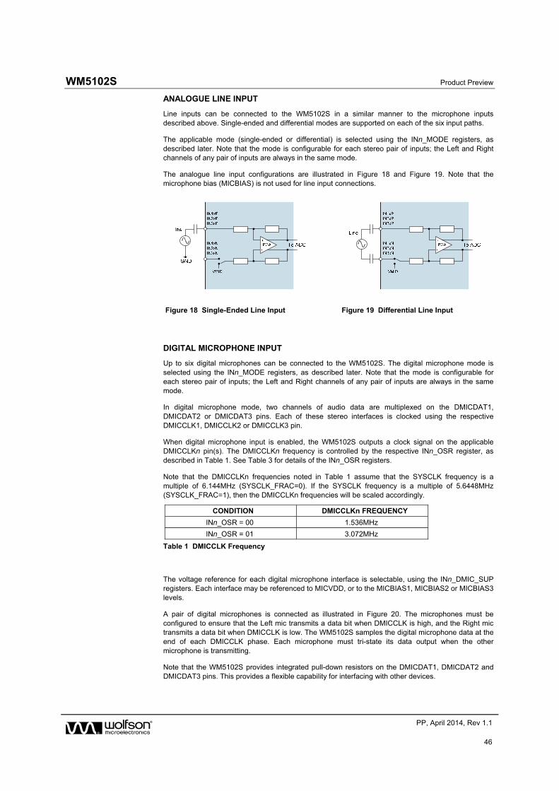
WM5102S Product Preview
w PP, April 2014, Rev 1.1
46
ANALOGUE LINE INPUT
Line inputs can be connected to the WM5102S in a similar manner to the microphone inputs described above. Single-ended and differential modes are supported on each of the six input paths.
The applicable mode (single-ended or differential) is selected using the INn_MODE registers, as described later. Note that the mode is configurable for each stereo pair of inputs; the Left and Right channels of any pair of inputs are always in the same mode.
The analogue line input configurations are illustrated in Figure 18 and Figure 19. Note that the microphone bias (MICBIAS) is not used for line input connections.
Figure 18 Single-Ended Line Input Figure 19 Differential Line Input
DIGITAL MICROPHONE INPUT
Up to six digital microphones can be connected to the WM5102S. The digital microphone mode is selected using the INn_MODE registers, as described later. Note that the mode is configurable for each stereo pair of inputs; the Left and Right channels of any pair of inputs are always in the same mode.
In digital microphone mode, two channels of audio data are multiplexed on the DMICDAT1, DMICDAT2 or DMICDAT3 pins. Each of these stereo interfaces is clocked using the respective DMICCLK1, DMICCLK2 or DMICCLK3 pin.
When digital microphone input is enabled, the WM5102S outputs a clock signal on the applicable DMICCLKn pin(s). The DMICCLKn frequency is controlled by the respective INn_OSR register, as described in Table 1. See Table 3 for details of the INn_OSR registers.
Note that the DMICCLKn frequencies noted in Table 1 assume that the SYSCLK frequency is a multiple of 6.144MHz (SYSCLK_FRAC=0). If the SYSCLK frequency is a multiple of 5.6448MHz (SYSCLK_FRAC=1), then the DMICCLKn frequencies will be scaled accordingly.
CONDITION DMICCLKn FREQUENCY
INn_OSR = 00 1.536MHz
INn_OSR = 01 3.072MHz
Table 1 DMICCLK Frequency
The voltage reference for each digital microphone interface is selectable, using the INn_DMIC_SUP registers. Each interface may be referenced to MICVDD, or to the MICBIAS1, MICBIAS2 or MICBIAS3 levels.
A pair of digital microphones is connected as illustrated in Figure 20. The microphones must be configured to ensure that the Left mic transmits a data bit when DMICCLK is high, and the Right mic transmits a data bit when DMICCLK is low. The WM5102S samples the digital microphone data at the end of each DMICCLK phase. Each microphone must tri-state its data output when the other microphone is transmitting.
Note that the WM5102S provides integrated pull-down resistors on the DMICDAT1, DMICDAT2 and DMICDAT3 pins. This provides a flexible capability for interfacing with other devices.
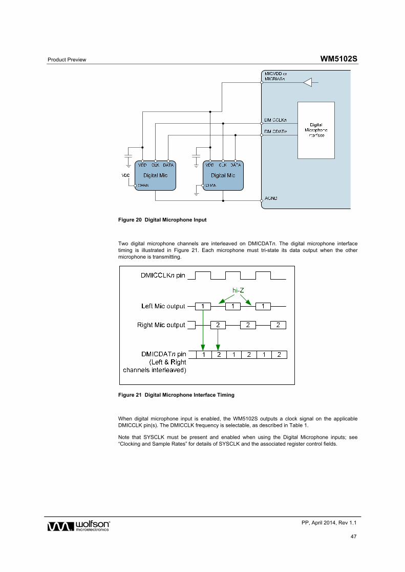
Product Preview WM5102S
w PP, April 2014, Rev 1.1
47
Figure 20 Digital Microphone Input
Two digital microphone channels are interleaved on DMICDATn. The digital microphone interface timing is illustrated in Figure 21. Each microphone must tri-state its data output when the other microphone is transmitting.
Figure 21 Digital Microphone Interface Timing
When digital microphone input is enabled, the WM5102S outputs a clock signal on the applicable DMICCLK pin(s). The DMICCLK frequency is selectable, as described in Table 1.
Note that SYSCLK must be present and enabled when using the Digital Microphone inputs; see “Clocking and Sample Rates” for details of SYSCLK and the associated register control fields.
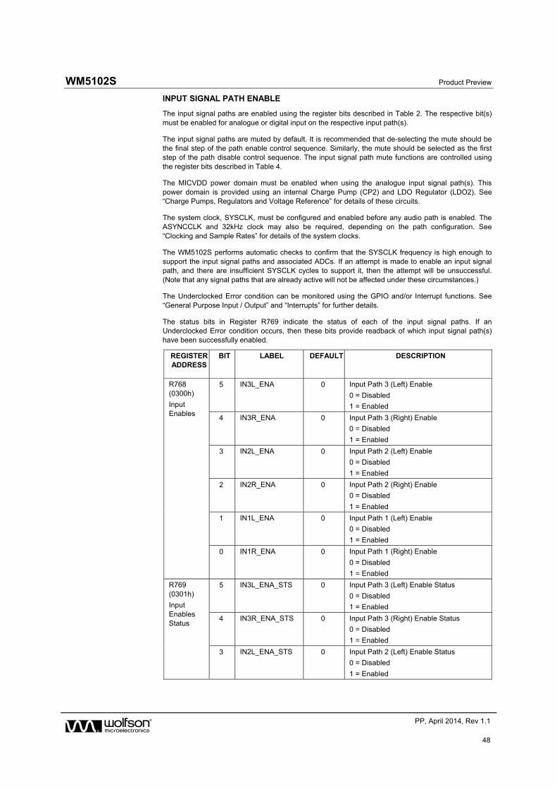
WM5102S Product Preview
w PP, April 2014, Rev 1.1
48
INPUT SIGNAL PATH ENABLE
The input signal paths are enabled using the register bits described in Table 2. The respective bit(s) must be enabled for analogue or digital input on the respective input path(s).
The input signal paths are muted by default. It is recommended that de-selecting the mute should be the final step of the path enable control sequence. Similarly, the mute should be selected as the first step of the path disable control sequence. The input signal path mute functions are controlled using the register bits described in Table 4.
The MICVDD power domain must be enabled when using the analogue input signal path(s). This power domain is provided using an internal Charge Pump (CP2) and LDO Regulator (LDO2). See “Charge Pumps, Regulators and Voltage Reference” for details of these circuits.
The system clock, SYSCLK, must be configured and enabled before any audio path is enabled. The ASYNCCLK and 32kHz clock may also be required, depending on the path configuration. See “Clocking and Sample Rates” for details of the system clocks.
The WM5102S performs automatic checks to confirm that the SYSCLK frequency is high enough to support the input signal paths and associated ADCs. If an attempt is made to enable an input signal path, and there are insufficient SYSCLK cycles to support it, then the attempt will be unsuccessful. (Note that any signal paths that are already active will not be affected under these circumstances.)
The Underclocked Error condition can be monitored using the GPIO and/or Interrupt functions. See “General Purpose Input / Output” and “Interrupts” for further details.
The status bits in Register R769 indicate the status of each of the input signal paths. If an Underclocked Error condition occurs, then these bits provide readback of which input signal path(s) have been successfully enabled.
REGISTER ADDRESS
BIT LABEL DEFAULT DESCRIPTION
R768 (0300h)
Input Enables
5 IN3L_ENA 0 Input Path 3 (Left) Enable
0 = Disabled
1 = Enabled
4 IN3R_ENA 0 Input Path 3 (Right) Enable
0 = Disabled
1 = Enabled
3 IN2L_ENA 0 Input Path 2 (Left) Enable
0 = Disabled
1 = Enabled
2 IN2R_ENA 0 Input Path 2 (Right) Enable
0 = Disabled
1 = Enabled
1 IN1L_ENA 0 Input Path 1 (Left) Enable
0 = Disabled
1 = Enabled
0 IN1R_ENA 0 Input Path 1 (Right) Enable
0 = Disabled
1 = Enabled
R769 (0301h)
Input Enables Status
5 IN3L_ENA_STS 0 Input Path 3 (Left) Enable Status
0 = Disabled
1 = Enabled
4 IN3R_ENA_STS 0 Input Path 3 (Right) Enable Status
0 = Disabled
1 = Enabled
3 IN2L_ENA_STS 0 Input Path 2 (Left) Enable Status
0 = Disabled
1 = Enabled
Product Preview WM5102S
w PP, April 2014, Rev 1.1
49
REGISTER ADDRESS
BIT LABEL DEFAULT DESCRIPTION
2 IN2R_ENA_STS 0 Input Path 2 (Right) Enable Status
0 = Disabled
1 = Enabled
1 IN1L_ENA_STS 0 Input Path 1 (Left) Enable Status
0 = Disabled
1 = Enabled
0 IN1R_ENA_STS 0 Input Path 1 (Right) Enable Status
0 = Disabled
1 = Enabled
Table 2 Input Signal Path Enable
INPUT SIGNAL PATH SAMPLE RATE CONTROL
The input signal paths may be selected as input to the digital mixers or signal processing functions within the WM5102S digital core. The sample rate for the input signal paths is configured using the IN_RATE register - see Table 21 within the “Digital Core” section.
Note that sample rate conversion is required when routing the input signal paths to any signal chain that is asynchronous and/or configured for a different sample rate.
INPUT SIGNAL PATH CONFIGURATION
The WM5102S supports six input signal paths. Each pair of inputs can be configured as single-ended, differential, or digital microphone configuration. Note that the mode is configurable for each stereo pair of inputs; the Left and Right channels of any pair of inputs are always in the same mode.
The input signal path configuration is selected using the INn_MODE registers (where ‘n’ identifies the associated input). The external circuit configurations are illustrated on the previous pages.
The analogue input signal paths (single-ended or differential) each incorporate a PGA to provide gain in the range 0dB to +31dB in 1dB steps. Note that these PGAs do not provide pop suppression functions; it is recommended that the gain should not be adjusted whilst the respective signal path is enabled.
The analogue input PGA gain is controlled using the INnL_PGA_VOL and INnR_PGA_VOL registers. Note that separate volume control is provided for the Left and Right channels of each stereo pair.
When the input signal path is configured for digital microphone input, the voltage reference for the associated input/output pins is selectable using the INn_DMIC_SUP registers - each interface may be referenced to MICVDD, or to the MICBIAS1, MICBIAS2 or MICBIAS3 levels.
A digital delay may be applied to any of the digital microphone input channels. This feature can be used for phase adjustment of any digital input, including directional control of multiple microphones. The delay is controlled using the INnL_DMIC_DLY and INnR_DMIC_DLY registers.
The MICVDD voltage is generated by an internal Charge Pump and LDO Regulator. The MICBIAS1, MICBIAS2 and MICBIAS3 outputs are derived from MICVDD - see “Charge Pumps, Regulators and Voltage Reference”.
Under default register conditions, the input signal paths are configured for highest performance. This can be adjusted using the INn_OSR registers, which provide control of the DMICCLKn frequency and the ADC oversample rate.
The input signal paths are configured using the register bits described in Table 3.
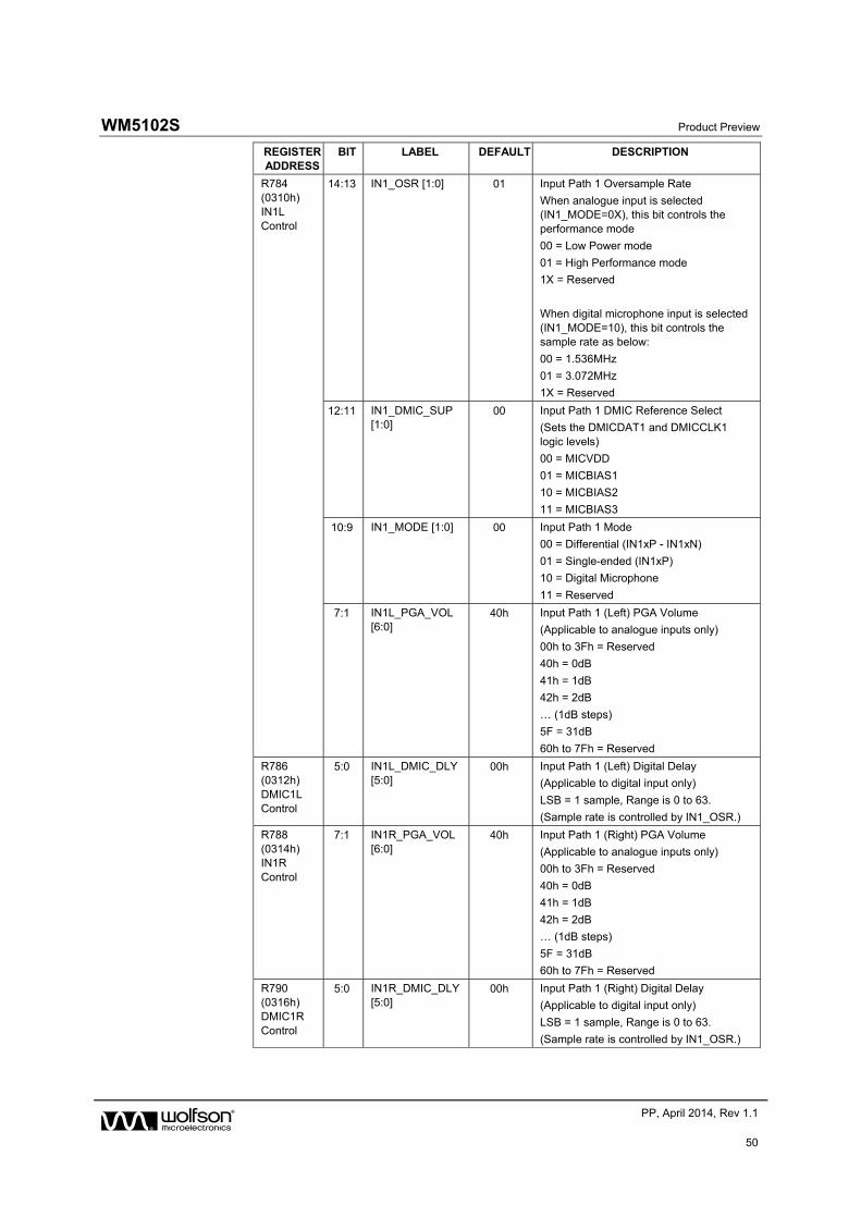
WM5102S Product Preview
w PP, April 2014, Rev 1.1
50
REGISTER ADDRESS
BIT LABEL DEFAULT DESCRIPTION
R784 (0310h) IN1L Control
14:13 IN1_OSR [1:0] 01 Input Path 1 Oversample Rate
When analogue input is selected (IN1_MODE=0X), this bit controls the performance mode
00 = Low Power mode
01 = High Performance mode
1X = Reserved
When digital microphone input is selected (IN1_MODE=10), this bit controls the sample rate as below:
00 = 1.536MHz
01 = 3.072MHz
1X = Reserved
12:11 IN1_DMIC_SUP [1:0]
00 Input Path 1 DMIC Reference Select
(Sets the DMICDAT1 and DMICCLK1 logic levels)
00 = MICVDD
01 = MICBIAS1
10 = MICBIAS2
11 = MICBIAS3
10:9 IN1_MODE [1:0] 00 Input Path 1 Mode
00 = Differential (IN1xP - IN1xN)
01 = Single-ended (IN1xP)
10 = Digital Microphone
11 = Reserved
7:1 IN1L_PGA_VOL [6:0]
40h Input Path 1 (Left) PGA Volume
(Applicable to analogue inputs only)
00h to 3Fh = Reserved
40h = 0dB
41h = 1dB
42h = 2dB
… (1dB steps)
5F = 31dB
60h to 7Fh = Reserved
R786 (0312h) DMIC1L Control
5:0 IN1L_DMIC_DLY [5:0]
00h Input Path 1 (Left) Digital Delay
(Applicable to digital input only)
LSB = 1 sample, Range is 0 to 63.
(Sample rate is controlled by IN1_OSR.)
R788 (0314h) IN1R Control
7:1 IN1R_PGA_VOL [6:0]
40h Input Path 1 (Right) PGA Volume
(Applicable to analogue inputs only)
00h to 3Fh = Reserved
40h = 0dB
41h = 1dB
42h = 2dB
… (1dB steps)
5F = 31dB
60h to 7Fh = Reserved
R790 (0316h) DMIC1R Control
5:0 IN1R_DMIC_DLY [5:0]
00h Input Path 1 (Right) Digital Delay
(Applicable to digital input only)
LSB = 1 sample, Range is 0 to 63.
(Sample rate is controlled by IN1_OSR.)
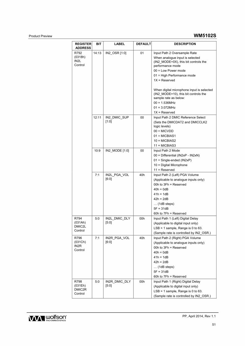
Product Preview WM5102S
w PP, April 2014, Rev 1.1
51
REGISTER ADDRESS
BIT LABEL DEFAULT DESCRIPTION
R792 (0318h) IN2L Control
14:13 IN2_OSR [1:0] 01 Input Path 2 Oversample Rate
When analogue input is selected (IN2_MODE=0X), this bit controls the performance mode
00 = Low Power mode
01 = High Performance mode
1X = Reserved
When digital microphone input is selected (IN2_MODE=10), this bit controls the sample rate as below:
00 = 1.536MHz
01 = 3.072MHz
1X = Reserved
12:11 IN2_DMIC_SUP [1:0]
00 Input Path 2 DMIC Reference Select
(Sets the DMICDAT2 and DMICCLK2 logic levels)
00 = MICVDD
01 = MICBIAS1
10 = MICBIAS2
11 = MICBIAS3
10:9 IN2_MODE [1:0] 00 Input Path 2 Mode
00 = Differential (IN2xP - IN2xN)
01 = Single-ended (IN2xP)
10 = Digital Microphone
11 = Reserved
7:1 IN2L_PGA_VOL [6:0]
40h Input Path 2 (Left) PGA Volume
(Applicable to analogue inputs only)
00h to 3Fh = Reserved
40h = 0dB
41h = 1dB
42h = 2dB
… (1dB steps)
5F = 31dB
60h to 7Fh = Reserved
R794 (031Ah) DMIC2L Control
5:0 IN2L_DMIC_DLY [5:0]
00h Input Path 1 (Left) Digital Delay
(Applicable to digital input only)
LSB = 1 sample, Range is 0 to 63.
(Sample rate is controlled by IN2_OSR.)
R796 (031Ch) IN2R Control
7:1 IN2R_PGA_VOL [6:0]
40h Input Path 2 (Right) PGA Volume
(Applicable to analogue inputs only)
00h to 3Fh = Reserved
40h = 0dB
41h = 1dB
42h = 2dB
… (1dB steps)
5F = 31dB
60h to 7Fh = Reserved
R798 (031Eh) DMIC2R Control
5:0 IN2R_DMIC_DLY [5:0]
00h Input Path 1 (Right) Digital Delay
(Applicable to digital input only)
LSB = 1 sample, Range is 0 to 63.
(Sample rate is controlled by IN2_OSR.)
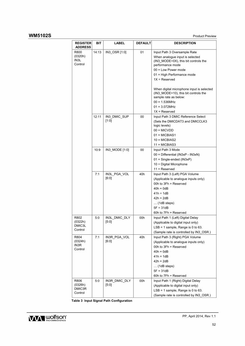
WM5102S Product Preview
w PP, April 2014, Rev 1.1
52
REGISTER ADDRESS
BIT LABEL DEFAULT DESCRIPTION
R800 (0320h) IN3L Control
14:13 IN3_OSR [1:0] 01 Input Path 3 Oversample Rate
When analogue input is selected (IN3_MODE=0X), this bit controls the performance mode
00 = Low Power mode
01 = High Performance mode
1X = Reserved
When digital microphone input is selected (IN3_MODE=10), this bit controls the sample rate as below:
00 = 1.536MHz
01 = 3.072MHz
1X = Reserved
12:11 IN3_DMIC_SUP [1:0]
00 Input Path 3 DMIC Reference Select
(Sets the DMICDAT3 and DMICCLK3 logic levels)
00 = MICVDD
01 = MICBIAS1
10 = MICBIAS2
11 = MICBIAS3
10:9 IN3_MODE [1:0] 00 Input Path 3 Mode
00 = Differential (IN3xP - IN3xN)
01 = Single-ended (IN3xP)
10 = Digital Microphone
11 = Reserved
7:1 IN3L_PGA_VOL [6:0]
40h Input Path 3 (Left) PGA Volume
(Applicable to analogue inputs only)
00h to 3Fh = Reserved
40h = 0dB
41h = 1dB
42h = 2dB
… (1dB steps)
5F = 31dB
60h to 7Fh = Reserved
R802 (0322h) DMIC3L Control
5:0 IN3L_DMIC_DLY [5:0]
00h Input Path 1 (Left) Digital Delay
(Applicable to digital input only)
LSB = 1 sample, Range is 0 to 63.
(Sample rate is controlled by IN3_OSR.)
R804 (0324h) IN3R Control
7:1 IN3R_PGA_VOL [6:0]
40h Input Path 3 (Right) PGA Volume
(Applicable to analogue inputs only)
00h to 3Fh = Reserved
40h = 0dB
41h = 1dB
42h = 2dB
… (1dB steps)
5F = 31dB
60h to 7Fh = Reserved
R806 (0326h) DMIC3R Control
5:0 IN3R_DMIC_DLY [5:0]
00h Input Path 1 (Right) Digital Delay
(Applicable to digital input only)
LSB = 1 sample, Range is 0 to 63.
(Sample rate is controlled by IN3_OSR.)
Table 3 Input Signal Path Configuration
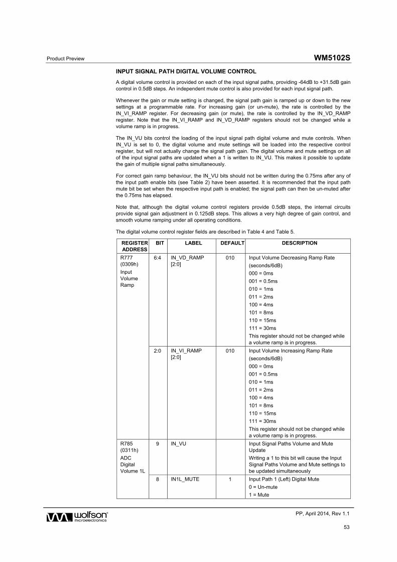
Product Preview WM5102S
w PP, April 2014, Rev 1.1
53
INPUT SIGNAL PATH DIGITAL VOLUME CONTROL
A digital volume control is provided on each of the input signal paths, providing -64dB to +31.5dB gain control in 0.5dB steps. An independent mute control is also provided for each input signal path.
Whenever the gain or mute setting is changed, the signal path gain is ramped up or down to the new settings at a programmable rate. For increasing gain (or un-mute), the rate is controlled by the IN_VI_RAMP register. For decreasing gain (or mute), the rate is controlled by the IN_VD_RAMP register. Note that the IN_VI_RAMP and IN_VD_RAMP registers should not be changed while a volume ramp is in progress.
The IN_VU bits control the loading of the input signal path digital volume and mute controls. When IN_VU is set to 0, the digital volume and mute settings will be loaded into the respective control register, but will not actually change the signal path gain. The digital volume and mute settings on all of the input signal paths are updated when a 1 is written to IN_VU. This makes it possible to update the gain of multiple signal paths simultaneously.
For correct gain ramp behaviour, the IN_VU bits should not be written during the 0.75ms after any of the input path enable bits (see Table 2) have been asserted. It is recommended that the input path mute bit be set when the respective input path is enabled; the signal path can then be un-muted after the 0.75ms has elapsed.
Note that, although the digital volume control registers provide 0.5dB steps, the internal circuits provide signal gain adjustment in 0.125dB steps. This allows a very high degree of gain control, and smooth volume ramping under all operating conditions.
The digital volume control register fields are described in Table 4 and Table 5.
REGISTER ADDRESS
BIT LABEL DEFAULT DESCRIPTION
R777 (0309h)
Input Volume Ramp
6:4 IN_VD_RAMP [2:0]
010 Input Volume Decreasing Ramp Rate
(seconds/6dB)
000 = 0ms
001 = 0.5ms
010 = 1ms
011 = 2ms
100 = 4ms
101 = 8ms
110 = 15ms
111 = 30ms
This register should not be changed while a volume ramp is in progress.
2:0 IN_VI_RAMP [2:0]
010 Input Volume Increasing Ramp Rate
(seconds/6dB)
000 = 0ms
001 = 0.5ms
010 = 1ms
011 = 2ms
100 = 4ms
101 = 8ms
110 = 15ms
111 = 30ms
This register should not be changed while a volume ramp is in progress.
R785 (0311h)
ADC Digital Volume 1L
9 IN_VU Input Signal Paths Volume and Mute Update
Writing a 1 to this bit will cause the Input Signal Paths Volume and Mute settings to be updated simultaneously
8 IN1L_MUTE 1 Input Path 1 (Left) Digital Mute
0 = Un-mute
1 = Mute
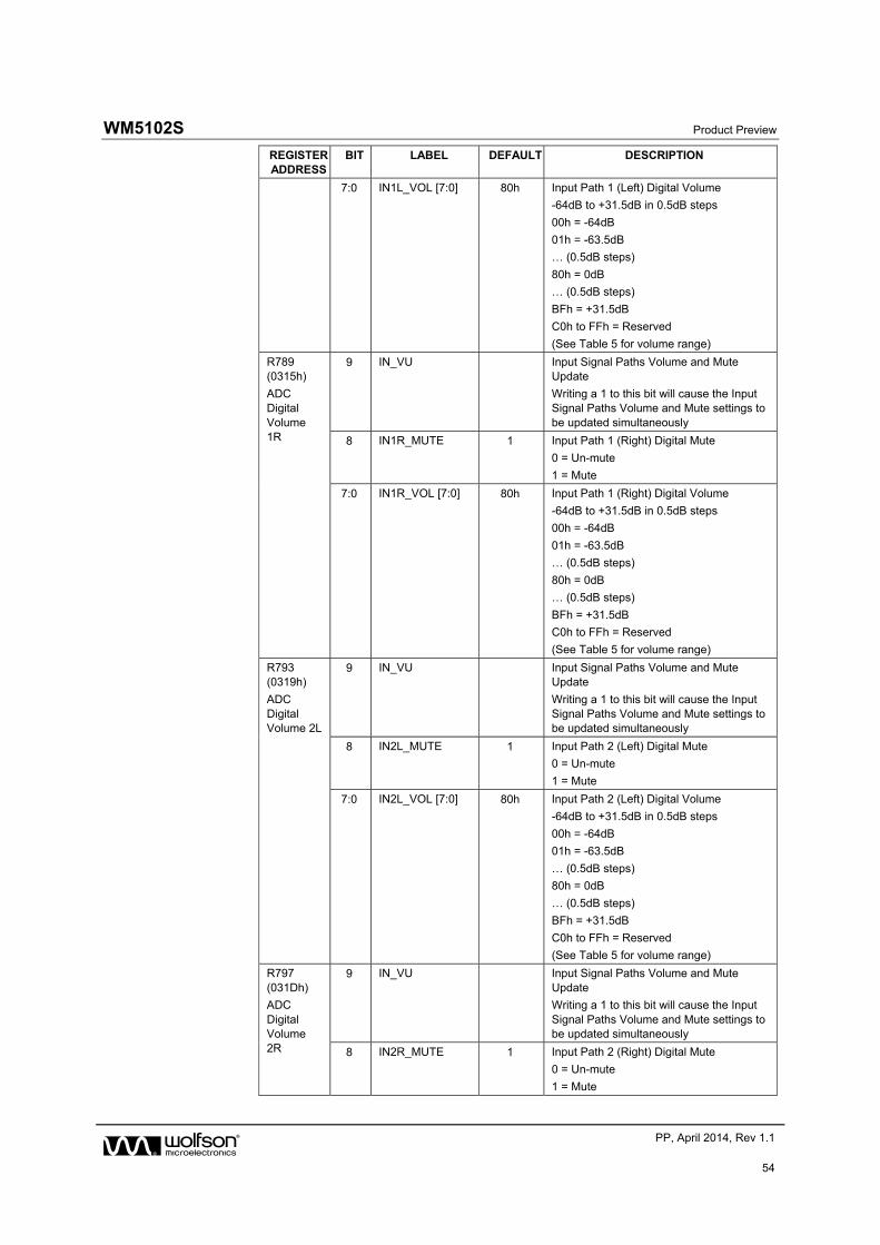
WM5102S Product Preview
w PP, April 2014, Rev 1.1
54
REGISTER ADDRESS
BIT LABEL DEFAULT DESCRIPTION
7:0 IN1L_VOL [7:0] 80h Input Path 1 (Left) Digital Volume
-64dB to +31.5dB in 0.5dB steps
00h = -64dB
01h = -63.5dB
… (0.5dB steps)
80h = 0dB
… (0.5dB steps)
BFh = +31.5dB
C0h to FFh = Reserved
(See Table 5 for volume range)
R789 (0315h)
ADC Digital Volume 1R
9 IN_VU Input Signal Paths Volume and Mute Update
Writing a 1 to this bit will cause the Input Signal Paths Volume and Mute settings to be updated simultaneously
8 IN1R_MUTE 1 Input Path 1 (Right) Digital Mute
0 = Un-mute
1 = Mute
7:0 IN1R_VOL [7:0] 80h Input Path 1 (Right) Digital Volume
-64dB to +31.5dB in 0.5dB steps
00h = -64dB
01h = -63.5dB
… (0.5dB steps)
80h = 0dB
… (0.5dB steps)
BFh = +31.5dB
C0h to FFh = Reserved
(See Table 5 for volume range)
R793 (0319h)
ADC Digital Volume 2L
9 IN_VU Input Signal Paths Volume and Mute Update
Writing a 1 to this bit will cause the Input Signal Paths Volume and Mute settings to be updated simultaneously
8 IN2L_MUTE 1 Input Path 2 (Left) Digital Mute
0 = Un-mute
1 = Mute
7:0 IN2L_VOL [7:0] 80h Input Path 2 (Left) Digital Volume
-64dB to +31.5dB in 0.5dB steps
00h = -64dB
01h = -63.5dB
… (0.5dB steps)
80h = 0dB
… (0.5dB steps)
BFh = +31.5dB
C0h to FFh = Reserved
(See Table 5 for volume range)
R797 (031Dh)
ADC Digital Volume 2R
9 IN_VU Input Signal Paths Volume and Mute Update
Writing a 1 to this bit will cause the Input Signal Paths Volume and Mute settings to be updated simultaneously
8 IN2R_MUTE 1 Input Path 2 (Right) Digital Mute
0 = Un-mute
1 = Mute
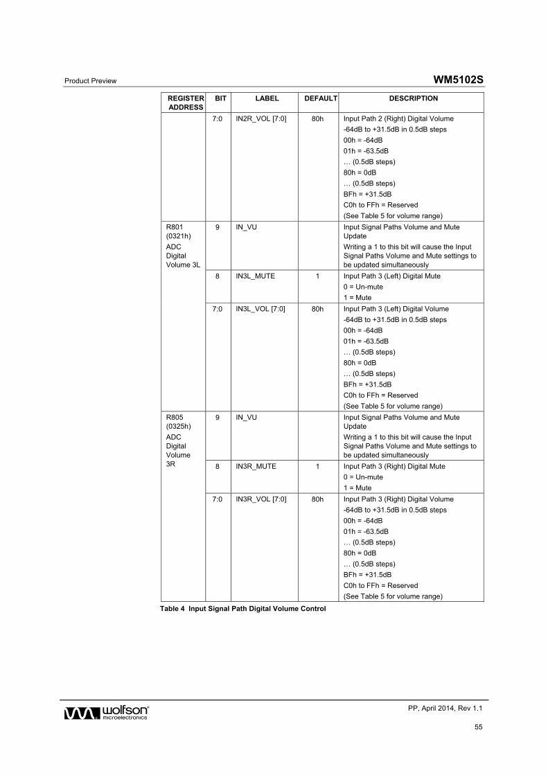
Product Preview WM5102S
w PP, April 2014, Rev 1.1
55
REGISTER ADDRESS
BIT LABEL DEFAULT DESCRIPTION
7:0 IN2R_VOL [7:0] 80h Input Path 2 (Right) Digital Volume
-64dB to +31.5dB in 0.5dB steps
00h = -64dB
01h = -63.5dB
… (0.5dB steps)
80h = 0dB
… (0.5dB steps)
BFh = +31.5dB
C0h to FFh = Reserved
(See Table 5 for volume range)
R801 (0321h)
ADC Digital Volume 3L
9 IN_VU Input Signal Paths Volume and Mute Update
Writing a 1 to this bit will cause the Input Signal Paths Volume and Mute settings to be updated simultaneously
8 IN3L_MUTE 1 Input Path 3 (Left) Digital Mute
0 = Un-mute
1 = Mute
7:0 IN3L_VOL [7:0] 80h Input Path 3 (Left) Digital Volume
-64dB to +31.5dB in 0.5dB steps
00h = -64dB
01h = -63.5dB
… (0.5dB steps)
80h = 0dB
… (0.5dB steps)
BFh = +31.5dB
C0h to FFh = Reserved
(See Table 5 for volume range)
R805 (0325h)
ADC Digital Volume 3R
9 IN_VU Input Signal Paths Volume and Mute Update
Writing a 1 to this bit will cause the Input Signal Paths Volume and Mute settings to be updated simultaneously
8 IN3R_MUTE 1 Input Path 3 (Right) Digital Mute
0 = Un-mute
1 = Mute
7:0 IN3R_VOL [7:0] 80h Input Path 3 (Right) Digital Volume
-64dB to +31.5dB in 0.5dB steps
00h = -64dB
01h = -63.5dB
… (0.5dB steps)
80h = 0dB
… (0.5dB steps)
BFh = +31.5dB
C0h to FFh = Reserved
(See Table 5 for volume range)
Table 4 Input Signal Path Digital Volume Control
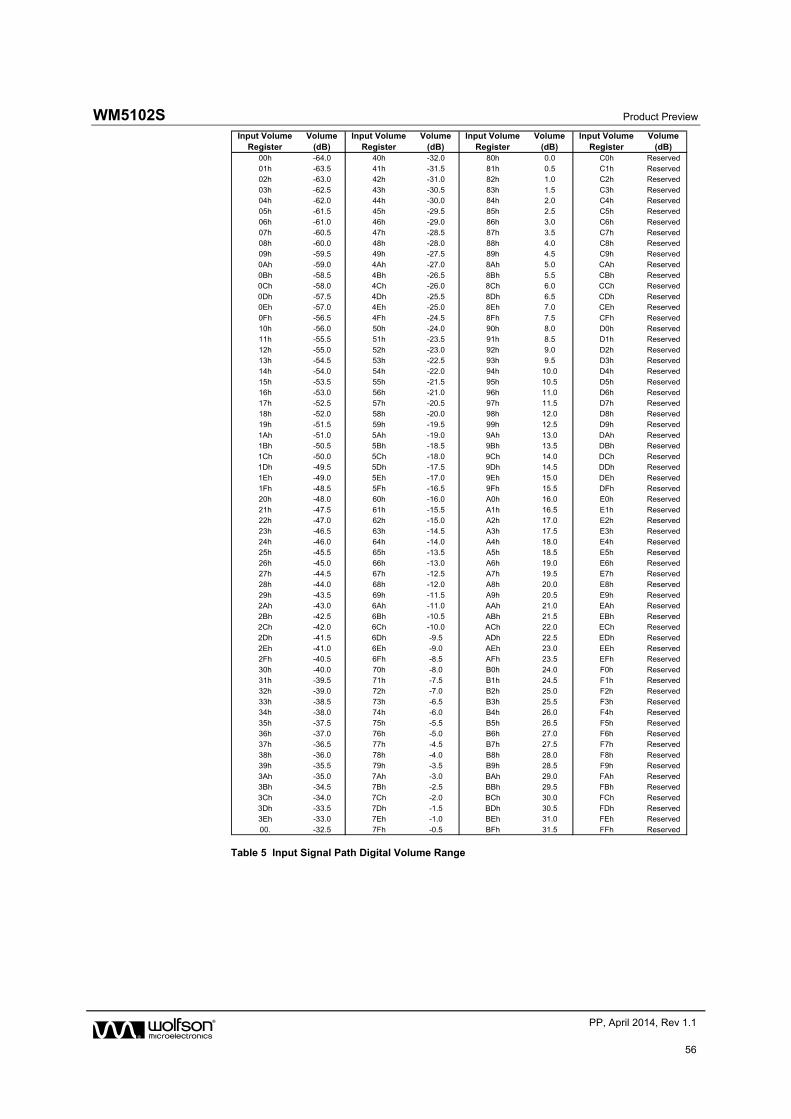
WM5102S Product Preview
w PP, April 2014, Rev 1.1
56
Input Volume Register
Volume (dB)
Input Volume Register
Volume (dB)
Input Volume Register
Volume (dB)
Input Volume Register
Volume (dB)
00h -64.0 40h -32.0 80h 0.0 C0h Reserved01h -63.5 41h -31.5 81h 0.5 C1h Reserved02h -63.0 42h -31.0 82h 1.0 C2h Reserved03h -62.5 43h -30.5 83h 1.5 C3h Reserved04h -62.0 44h -30.0 84h 2.0 C4h Reserved05h -61.5 45h -29.5 85h 2.5 C5h Reserved06h -61.0 46h -29.0 86h 3.0 C6h Reserved07h -60.5 47h -28.5 87h 3.5 C7h Reserved08h -60.0 48h -28.0 88h 4.0 C8h Reserved09h -59.5 49h -27.5 89h 4.5 C9h Reserved0Ah -59.0 4Ah -27.0 8Ah 5.0 CAh Reserved0Bh -58.5 4Bh -26.5 8Bh 5.5 CBh Reserved0Ch -58.0 4Ch -26.0 8Ch 6.0 CCh Reserved0Dh -57.5 4Dh -25.5 8Dh 6.5 CDh Reserved0Eh -57.0 4Eh -25.0 8Eh 7.0 CEh Reserved0Fh -56.5 4Fh -24.5 8Fh 7.5 CFh Reserved10h -56.0 50h -24.0 90h 8.0 D0h Reserved11h -55.5 51h -23.5 91h 8.5 D1h Reserved12h -55.0 52h -23.0 92h 9.0 D2h Reserved13h -54.5 53h -22.5 93h 9.5 D3h Reserved14h -54.0 54h -22.0 94h 10.0 D4h Reserved15h -53.5 55h -21.5 95h 10.5 D5h Reserved16h -53.0 56h -21.0 96h 11.0 D6h Reserved17h -52.5 57h -20.5 97h 11.5 D7h Reserved18h -52.0 58h -20.0 98h 12.0 D8h Reserved19h -51.5 59h -19.5 99h 12.5 D9h Reserved1Ah -51.0 5Ah -19.0 9Ah 13.0 DAh Reserved1Bh -50.5 5Bh -18.5 9Bh 13.5 DBh Reserved1Ch -50.0 5Ch -18.0 9Ch 14.0 DCh Reserved1Dh -49.5 5Dh -17.5 9Dh 14.5 DDh Reserved1Eh -49.0 5Eh -17.0 9Eh 15.0 DEh Reserved1Fh -48.5 5Fh -16.5 9Fh 15.5 DFh Reserved20h -48.0 60h -16.0 A0h 16.0 E0h Reserved21h -47.5 61h -15.5 A1h 16.5 E1h Reserved22h -47.0 62h -15.0 A2h 17.0 E2h Reserved23h -46.5 63h -14.5 A3h 17.5 E3h Reserved24h -46.0 64h -14.0 A4h 18.0 E4h Reserved25h -45.5 65h -13.5 A5h 18.5 E5h Reserved26h -45.0 66h -13.0 A6h 19.0 E6h Reserved27h -44.5 67h -12.5 A7h 19.5 E7h Reserved28h -44.0 68h -12.0 A8h 20.0 E8h Reserved29h -43.5 69h -11.5 A9h 20.5 E9h Reserved2Ah -43.0 6Ah -11.0 AAh 21.0 EAh Reserved2Bh -42.5 6Bh -10.5 ABh 21.5 EBh Reserved2Ch -42.0 6Ch -10.0 ACh 22.0 ECh Reserved2Dh -41.5 6Dh -9.5 ADh 22.5 EDh Reserved2Eh -41.0 6Eh -9.0 AEh 23.0 EEh Reserved2Fh -40.5 6Fh -8.5 AFh 23.5 EFh Reserved30h -40.0 70h -8.0 B0h 24.0 F0h Reserved31h -39.5 71h -7.5 B1h 24.5 F1h Reserved32h -39.0 72h -7.0 B2h 25.0 F2h Reserved33h -38.5 73h -6.5 B3h 25.5 F3h Reserved34h -38.0 74h -6.0 B4h 26.0 F4h Reserved35h -37.5 75h -5.5 B5h 26.5 F5h Reserved36h -37.0 76h -5.0 B6h 27.0 F6h Reserved37h -36.5 77h -4.5 B7h 27.5 F7h Reserved38h -36.0 78h -4.0 B8h 28.0 F8h Reserved39h -35.5 79h -3.5 B9h 28.5 F9h Reserved3Ah -35.0 7Ah -3.0 BAh 29.0 FAh Reserved3Bh -34.5 7Bh -2.5 BBh 29.5 FBh Reserved3Ch -34.0 7Ch -2.0 BCh 30.0 FCh Reserved3Dh -33.5 7Dh -1.5 BDh 30.5 FDh Reserved3Eh -33.0 7Eh -1.0 BEh 31.0 FEh Reserved00. -32.5 7Fh -0.5 BFh 31.5 FFh Reserved
Table 5 Input Signal Path Digital Volume Range
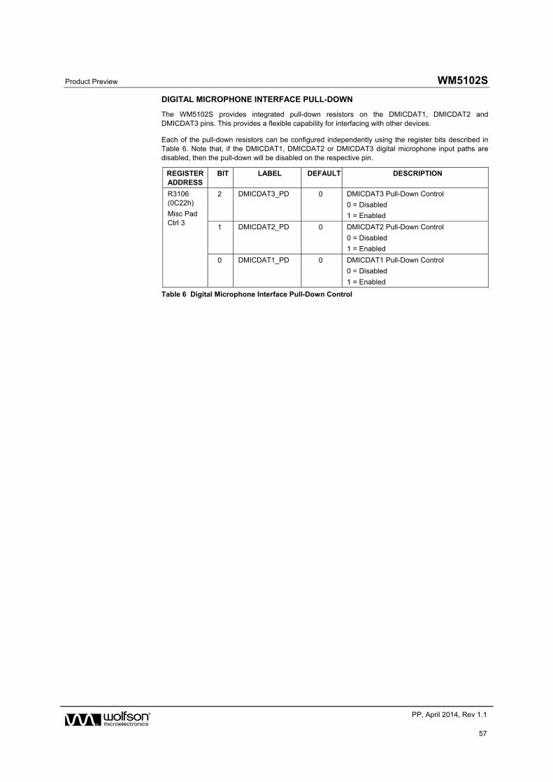
Product Preview WM5102S
w PP, April 2014, Rev 1.1
57
DIGITAL MICROPHONE INTERFACE PULL-DOWN
The WM5102S provides integrated pull-down resistors on the DMICDAT1, DMICDAT2 and DMICDAT3 pins. This provides a flexible capability for interfacing with other devices.
Each of the pull-down resistors can be configured independently using the register bits described in Table 6. Note that, if the DMICDAT1, DMICDAT2 or DMICDAT3 digital microphone input paths are disabled, then the pull-down will be disabled on the respective pin.
REGISTER ADDRESS
BIT LABEL DEFAULT DESCRIPTION
R3106 (0C22h)
Misc Pad Ctrl 3
2 DMICDAT3_PD 0 DMICDAT3 Pull-Down Control
0 = Disabled
1 = Enabled
1 DMICDAT2_PD 0 DMICDAT2 Pull-Down Control
0 = Disabled
1 = Enabled
0 DMICDAT1_PD 0 DMICDAT1 Pull-Down Control
0 = Disabled
1 = Enabled
Table 6 Digital Microphone Interface Pull-Down Control
WM5102S Product Preview
w PP, April 2014, Rev 1.1
58
DIGITAL CORE
The WM5102S digital core provides extensive mixing and processing capabilities for multiple signal paths. The configuration is highly flexible, and virtually every conceivable input/output connection can be supported between the available processing blocks.
The digital core provides parametric equalisation (EQ) functions, dynamic range control (DRC), low-pass / high-pass filters (LHPF), and programmable DSP capability. The DSP can support functions such as wind noise, side-tone or other programmable filters, also dynamic range control and compression, or virtual surround sound and other audio enhancements.
The WM5102S supports multiple signal paths through the digital core. Stereo full-duplex sample rate conversion is provided to allow digital audio to be routed between input (ADC) paths, output (DAC) paths, Digital Audio Interfaces (AIF1, AIF2 and AIF3) and SLIMbus paths operating at different sample rates and/or referenced to asynchronous clock domains.
The DSP functions are highly programmable, using application-specific control sequences. It should be noted that the DSP configuration data is lost whenever the DCVDD power domain is removed; the DSP configuration data must be downloaded to the WM5102S each time the device is powered up.
The procedure for configuring the WM5102S DSP functions is tailored to each customer’s application; please contact your local Wolfson representative for more details.
The WM5102S incorporates two 1kHz tone generators which can be used for ‘beep’ functions through any of the audio signal paths. A white noise generator is incorporated, to provide ‘comfort noise’ in cases where silence (digital mute) is not desirable.
A haptic signal generator is provided, for use with external haptic devices (eg. mechanical vibration actuators). Two Pulse Width Modulation (PWM) signal generators are also provided; the PWM waveforms can be modulated by an audio source within the digital core, and can be output on a GPIO pin.
An overview of the digital core processing and mixing functions is provided in Figure 22. An overview of the external digital interface paths is provided in Figure 23.
The control registers associated with the digital core signal paths are shown in Figure 24 through to Figure 41. The full list of digital mixer control registers is provided in the “Register Map” section (Register R1600 through to R2920). Generic register definitions are provided in Table 7.
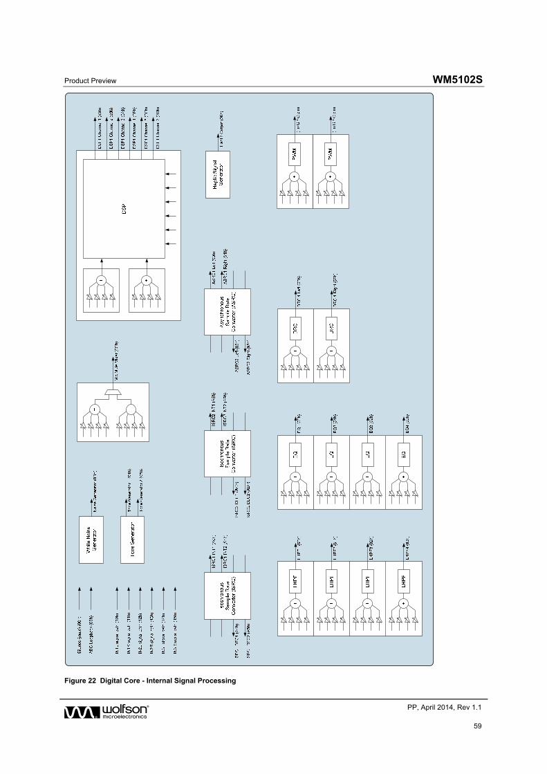
Product Preview WM5102S
w PP, April 2014, Rev 1.1
59
Figure 22 Digital Core - Internal Signal Processing
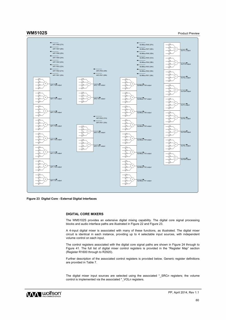
WM5102S Product Preview
w PP, April 2014, Rev 1.1
60
+AIF3 TX2 output
+AIF3 TX1 output
AIF3 RX1 (30h)
AIF3 RX2 (31h)
+AIF2 TX2 output
+AIF2 TX1 output
AIF2 RX1 (28h)
AIF2 RX2 (29h)
+AIF1 TX8 output
+AIF1 TX7 output
+AIF1 TX6 output
+AIF1 TX5 output
+AIF1 TX4 output
+AIF1 TX3 output
+AIF1 TX2 output
+AIF1 TX1 output
AIF1 RX3 (22h)
AIF1 RX4 (23h)
AIF1 RX5 (24h)
AIF1 RX6 (25h)
AIF1 RX7 (26h)
AIF1 RX8 (27h)
AIF1 RX1 (20h)
AIF1 RX2 (21h)
+SLIMbus TX8 output
+SLIMbus TX7 output
+SLIMbus TX6 output
+SLIMbus TX5 output
+SLIMbus TX4 output
+SLIMbus TX3 output
+SLIMbus TX2 output
+SLIMbus TX1 output
SLIMbus RX3 (3Ah)
SLIMbus RX4 (3Bh)
SLIMbus RX5 (3Ch)
SLIMbus RX6 (3Dh)
SLIMbus RX7 (3Eh)
SLIMbus RX8 (3Fh)
SLIMbus RX1 (38h)
SLIMbus RX2 (39h)
OUT5R output+
OUT5L output+
OUT4R output+
OUT4L output+
OUT3 output+
+OUT2R output
+OUT2L output
+OUT1R output
+OUT1L output
Figure 23 Digital Core - External Digital Interfaces
DIGITAL CORE MIXERS
The WM5102S provides an extensive digital mixing capability. The digital core signal processing blocks and audio interface paths are illustrated in Figure 22 and Figure 23.
A 4-input digital mixer is associated with many of these functions, as illustrated. The digital mixer circuit is identical in each instance, providing up to 4 selectable input sources, with independent volume control on each input.
The control registers associated with the digital core signal paths are shown in Figure 24 through to Figure 41. The full list of digital mixer control registers is provided in the “Register Map” section (Register R1600 through to R2920).
Further description of the associated control registers is provided below. Generic register definitions are provided in Table 7.
The digital mixer input sources are selected using the associated *_SRCn registers; the volume control is implemented via the associated *_VOLn registers.
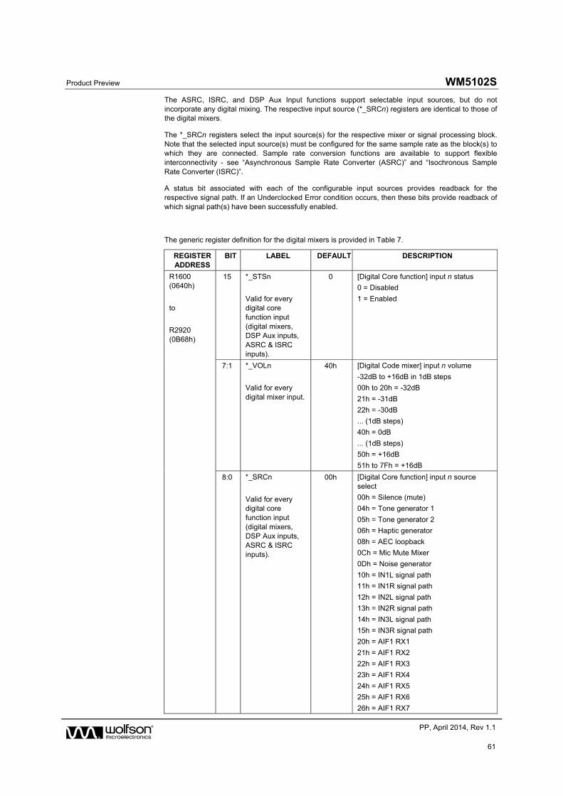
Product Preview WM5102S
w PP, April 2014, Rev 1.1
61
The ASRC, ISRC, and DSP Aux Input functions support selectable input sources, but do not incorporate any digital mixing. The respective input source (*_SRCn) registers are identical to those of the digital mixers.
The *_SRCn registers select the input source(s) for the respective mixer or signal processing block. Note that the selected input source(s) must be configured for the same sample rate as the block(s) to which they are connected. Sample rate conversion functions are available to support flexible interconnectivity - see “Asynchronous Sample Rate Converter (ASRC)” and “Isochronous Sample Rate Converter (ISRC)”.
A status bit associated with each of the configurable input sources provides readback for the respective signal path. If an Underclocked Error condition occurs, then these bits provide readback of which signal path(s) have been successfully enabled.
The generic register definition for the digital mixers is provided in Table 7.
REGISTER ADDRESS
BIT LABEL DEFAULT DESCRIPTION
R1600 (0640h)
to
R2920 (0B68h)
15 *_STSn
Valid for every digital core function input (digital mixers, DSP Aux inputs, ASRC & ISRC inputs).
0 [Digital Core function] input n status
0 = Disabled
1 = Enabled
7:1 *_VOLn
Valid for every digital mixer input.
40h [Digital Code mixer] input n volume
-32dB to +16dB in 1dB steps
00h to 20h = -32dB
21h = -31dB
22h = -30dB
... (1dB steps)
40h = 0dB
... (1dB steps)
50h = +16dB
51h to 7Fh = +16dB
8:0 *_SRCn
Valid for every digital core function input (digital mixers, DSP Aux inputs, ASRC & ISRC inputs).
00h [Digital Core function] input n source select
00h = Silence (mute)
04h = Tone generator 1
05h = Tone generator 2
06h = Haptic generator
08h = AEC loopback
0Ch = Mic Mute Mixer
0Dh = Noise generator
10h = IN1L signal path
11h = IN1R signal path
12h = IN2L signal path
13h = IN2R signal path
14h = IN3L signal path
15h = IN3R signal path
20h = AIF1 RX1
21h = AIF1 RX2
22h = AIF1 RX3
23h = AIF1 RX4
24h = AIF1 RX5
25h = AIF1 RX6
26h = AIF1 RX7
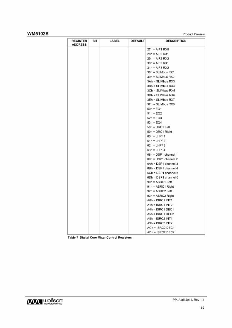
WM5102S Product Preview
w PP, April 2014, Rev 1.1
62
REGISTER ADDRESS
BIT LABEL DEFAULT DESCRIPTION
27h = AIF1 RX8
28h = AIF2 RX1
29h = AIF2 RX2
30h = AIF3 RX1
31h = AIF3 RX2
38h = SLIMbus RX1
39h = SLIMbus RX2
3Ah = SLIMbus RX3
3Bh = SLIMbus RX4
3Ch = SLIMbus RX5
3Dh = SLIMbus RX6
3Eh = SLIMbus RX7
3Fh = SLIMbus RX8
50h = EQ1
51h = EQ2
52h = EQ3
53h = EQ4
58h = DRC1 Left
59h = DRC1 Right
60h = LHPF1
61h = LHPF2
62h = LHPF3
63h = LHPF4
68h = DSP1 channel 1
69h = DSP1 channel 2
6Ah = DSP1 channel 3
6Bh = DSP1 channel 4
6Ch = DSP1 channel 5
6Dh = DSP1 channel 6
90h = ASRC1 Left
91h = ASRC1 Right
92h = ASRC2 Left
93h = ASRC2 Right
A0h = ISRC1 INT1
A1h = ISRC1 INT2
A4h = ISRC1 DEC1
A5h = ISRC1 DEC2
A8h = ISRC2 INT1
A9h = ISRC2 INT2
ACh = ISRC2 DEC1
ADh = ISRC2 DEC2
Table 7 Digital Core Mixer Control Registers
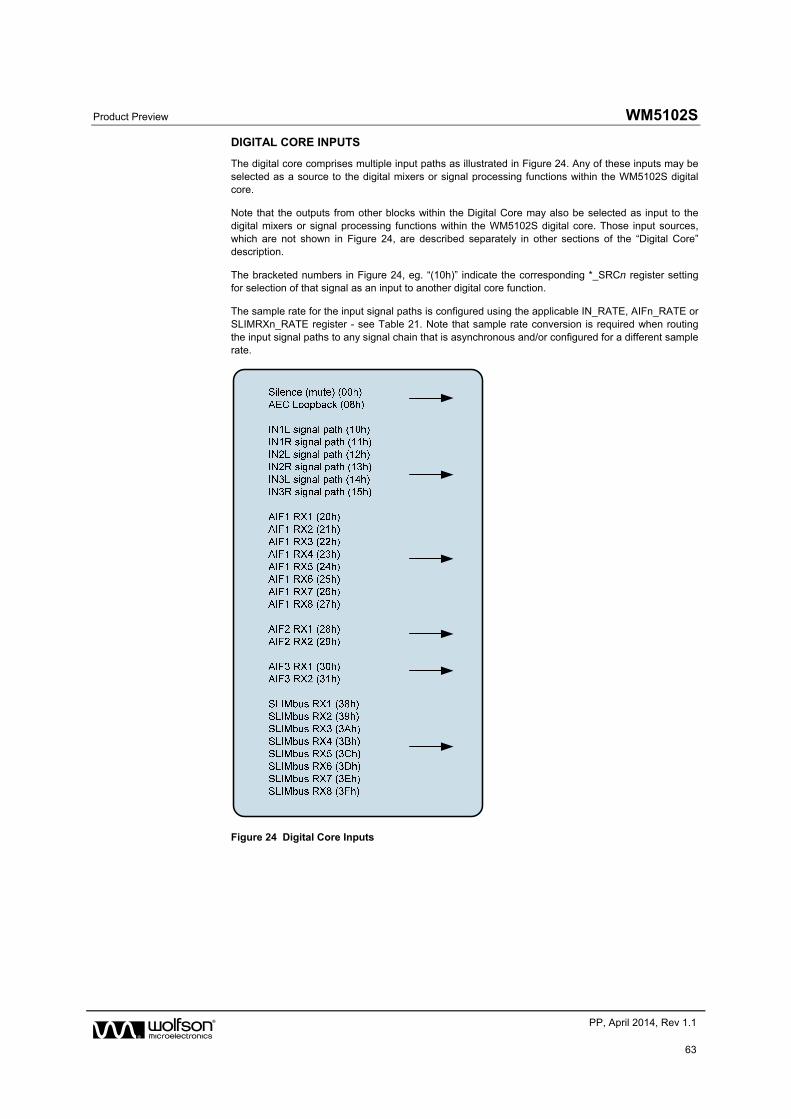
Product Preview WM5102S
w PP, April 2014, Rev 1.1
63
DIGITAL CORE INPUTS
The digital core comprises multiple input paths as illustrated in Figure 24. Any of these inputs may be selected as a source to the digital mixers or signal processing functions within the WM5102S digital core.
Note that the outputs from other blocks within the Digital Core may also be selected as input to the digital mixers or signal processing functions within the WM5102S digital core. Those input sources, which are not shown in Figure 24, are described separately in other sections of the “Digital Core” description.
The bracketed numbers in Figure 24, eg. “(10h)” indicate the corresponding *_SRCn register setting for selection of that signal as an input to another digital core function.
The sample rate for the input signal paths is configured using the applicable IN_RATE, AIFn_RATE or SLIMRXn_RATE register - see Table 21. Note that sample rate conversion is required when routing the input signal paths to any signal chain that is asynchronous and/or configured for a different sample rate.
Figure 24 Digital Core Inputs
WM5102S Product Preview
w PP, April 2014, Rev 1.1
64
DIGITAL CORE OUTPUT MIXERS
The digital core comprises multiple output paths. The output paths associated with AIF1, AIF2 and AIF3 are illustrated in Figure 25. The output paths associated with OUT1, OUT2, OUT3, OUT4 and OUT5 are illustrated in Figure 26. The output paths associated with the SLIMbus interface are illustrated in Figure 27.
A 4-input mixer is associated with each output. The 4 input sources are selectable in each case, and independent volume control is provided for each path.
The AIF1, AIF2 and AIF3 output mixer control registers (see Figure 25) are located at register addresses R1792 (700h) through to R1935 (78Fh). The OUT1, OUT2, OUT3, OUT4 and OUT5 output mixer control registers (see Figure 26) are located at addresses R1664 (680h) through to R1743 (06CFh). The SLIMbus output mixer control registers (see Figure 27) are located at addresses R1984 (7C0h) through to R2047 (7FFh).
The full list of digital mixer control registers is provided in the “Register Map” section (Register R1600 through to R2920). Generic register definitions are provided in Table 7.
The *_SRCn registers select the input source(s) for the respective mixers. Note that the selected input source(s) must be configured for the same sample rate as the mixer to which they are connected. Sample rate conversion functions are available to support flexible interconnectivity - see “Asynchronous Sample Rate Converter (ASRC)” and “Isochronous Sample Rate Converter (ISRC)”.
The sample rate for the output signal paths is configured using the applicable OUT_RATE, AIFn_RATE or SLIMTXn_RATE register - see Table 21. Note that sample rate conversion is required when routing the output signal paths to any signal chain that is asynchronous and/or configured for a different sample rate.
The WM5102S performs automatic checks to confirm that the SYSCLK frequency is high enough to support the output mixer paths. If an attempt is made to enable an output mixer path, and there are insufficient SYSCLK cycles to support it, then the attempt will be unsuccessful. (Note that any signal paths that are already active will not be affected under these circumstances.)
The Underclocked Error condition can be monitored using the GPIO and/or Interrupt functions. See “General Purpose Input / Output” and “Interrupts” for further details.
The status bits in Registers R1600 to R2920 indicate the status of each of the digital mixers. If an Underclocked Error condition occurs, then these bits provide readback of which mixer(s) have been successfully enabled.
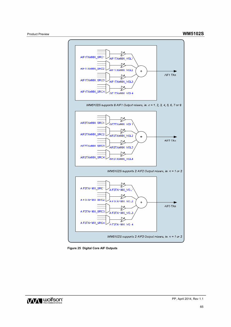
Product Preview WM5102S
w PP, April 2014, Rev 1.1
65
Figure 25 Digital Core AIF Outputs
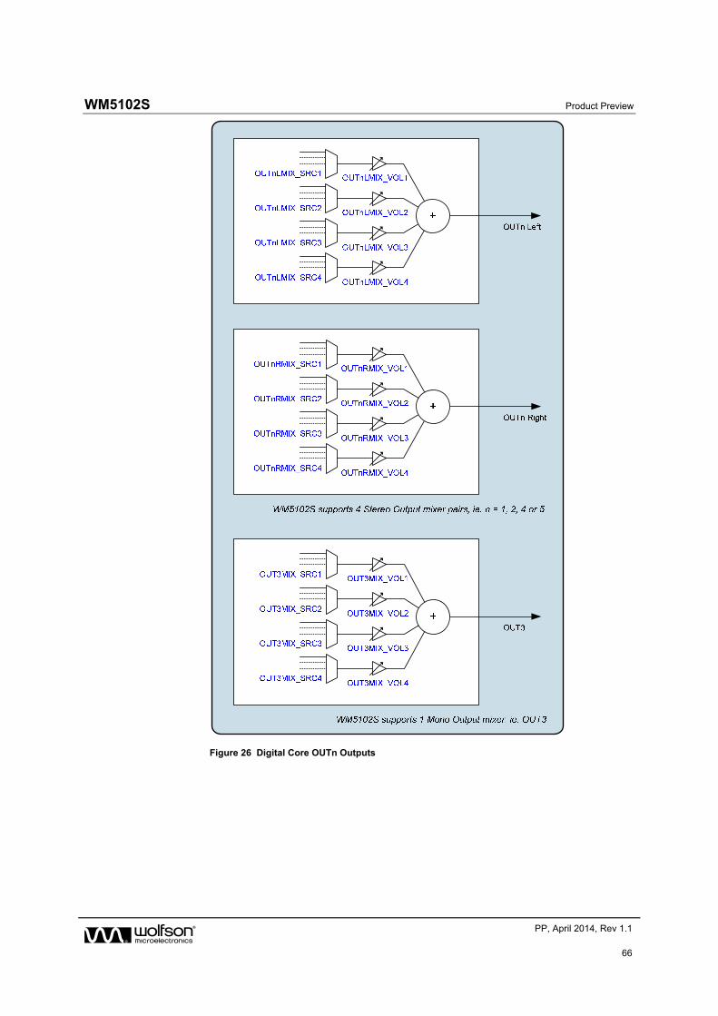
WM5102S Product Preview
w PP, April 2014, Rev 1.1
66
Figure 26 Digital Core OUTn Outputs
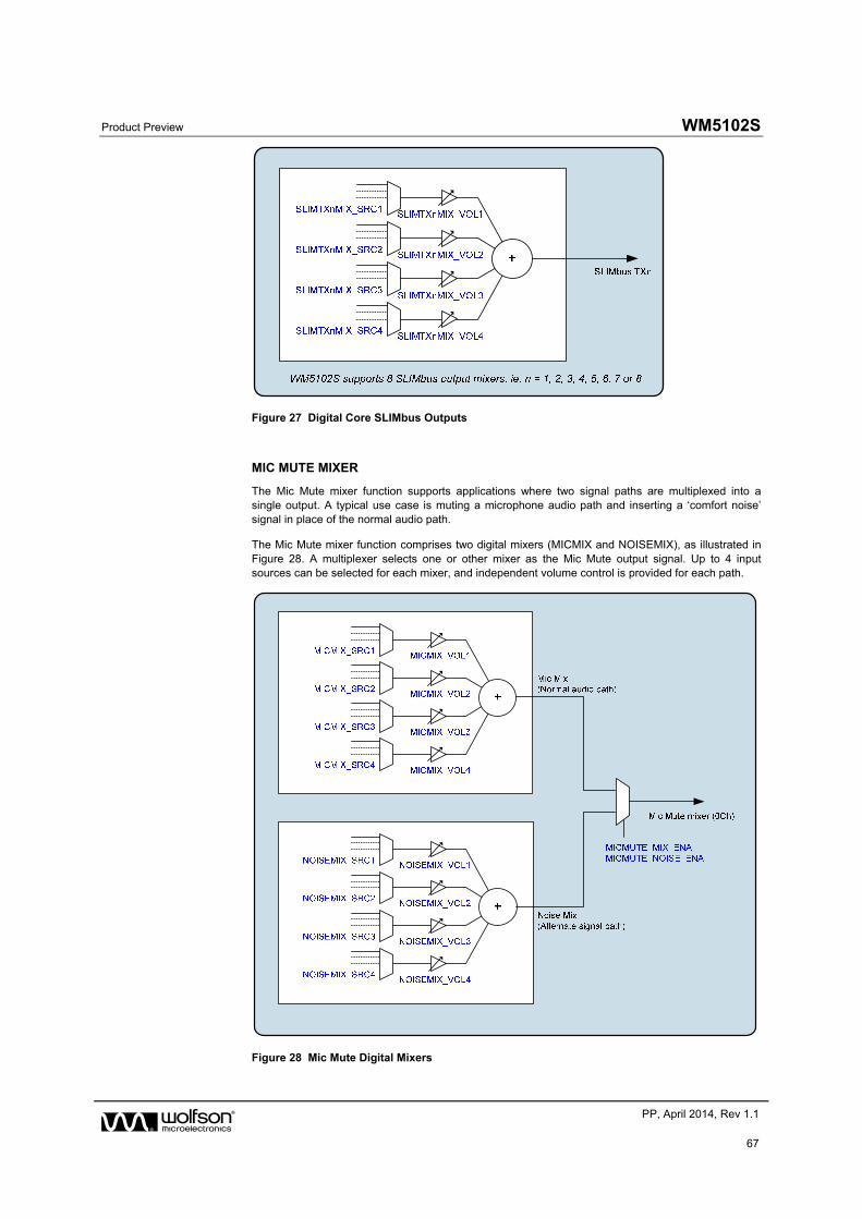
Product Preview WM5102S
w PP, April 2014, Rev 1.1
67
Figure 27 Digital Core SLIMbus Outputs
MIC MUTE MIXER
The Mic Mute mixer function supports applications where two signal paths are multiplexed into a single output. A typical use case is muting a microphone audio path and inserting a ‘comfort noise’ signal in place of the normal audio path.
The Mic Mute mixer function comprises two digital mixers (MICMIX and NOISEMIX), as illustrated in Figure 28. A multiplexer selects one or other mixer as the Mic Mute output signal. Up to 4 input sources can be selected for each mixer, and independent volume control is provided for each path.
Figure 28 Mic Mute Digital Mixers
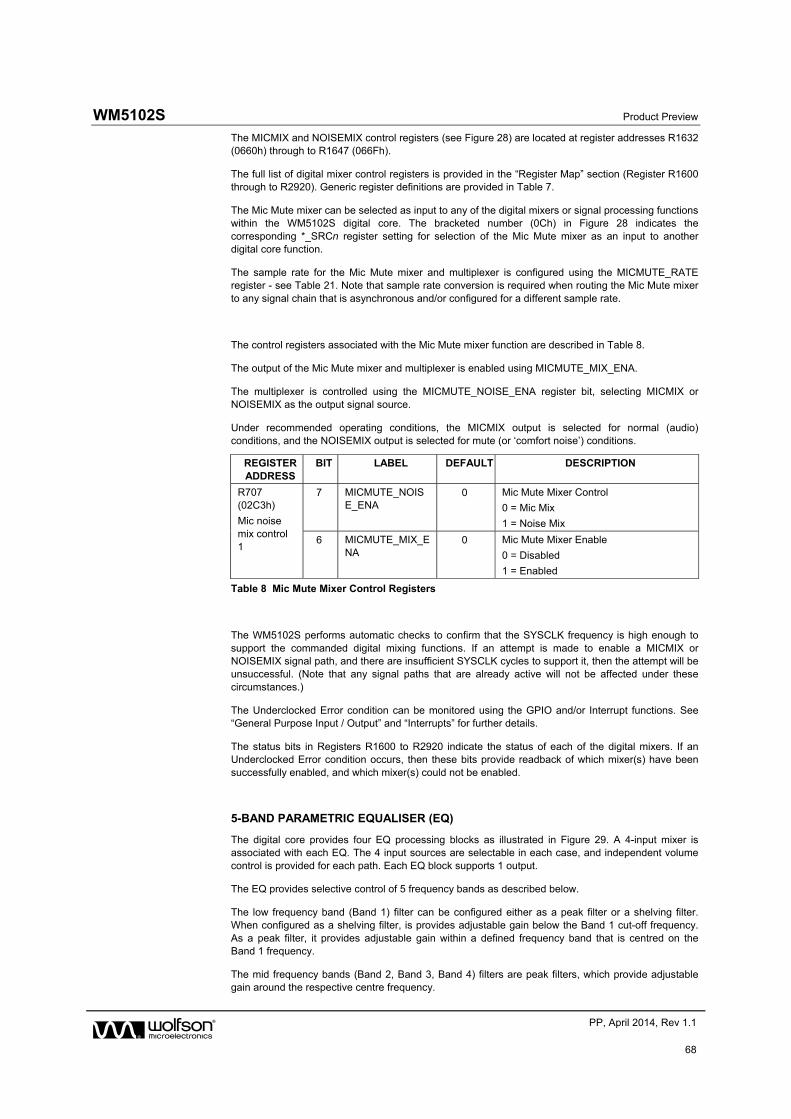
WM5102S Product Preview
w PP, April 2014, Rev 1.1
68
The MICMIX and NOISEMIX control registers (see Figure 28) are located at register addresses R1632 (0660h) through to R1647 (066Fh).
The full list of digital mixer control registers is provided in the “Register Map” section (Register R1600 through to R2920). Generic register definitions are provided in Table 7.
The Mic Mute mixer can be selected as input to any of the digital mixers or signal processing functions within the WM5102S digital core. The bracketed number (0Ch) in Figure 28 indicates the corresponding *_SRCn register setting for selection of the Mic Mute mixer as an input to another digital core function.
The sample rate for the Mic Mute mixer and multiplexer is configured using the MICMUTE_RATE register - see Table 21. Note that sample rate conversion is required when routing the Mic Mute mixer to any signal chain that is asynchronous and/or configured for a different sample rate.
The control registers associated with the Mic Mute mixer function are described in Table 8.
The output of the Mic Mute mixer and multiplexer is enabled using MICMUTE_MIX_ENA.
The multiplexer is controlled using the MICMUTE_NOISE_ENA register bit, selecting MICMIX or NOISEMIX as the output signal source.
Under recommended operating conditions, the MICMIX output is selected for normal (audio) conditions, and the NOISEMIX output is selected for mute (or ‘comfort noise’) conditions.
REGISTER ADDRESS
BIT LABEL DEFAULT DESCRIPTION
R707 (02C3h)
Mic noise mix control 1
7 MICMUTE_NOISE_ENA
0 Mic Mute Mixer Control
0 = Mic Mix
1 = Noise Mix
6 MICMUTE_MIX_ENA
0 Mic Mute Mixer Enable
0 = Disabled
1 = Enabled
Table 8 Mic Mute Mixer Control Registers
The WM5102S performs automatic checks to confirm that the SYSCLK frequency is high enough to support the commanded digital mixing functions. If an attempt is made to enable a MICMIX or NOISEMIX signal path, and there are insufficient SYSCLK cycles to support it, then the attempt will be unsuccessful. (Note that any signal paths that are already active will not be affected under these circumstances.)
The Underclocked Error condition can be monitored using the GPIO and/or Interrupt functions. See “General Purpose Input / Output” and “Interrupts” for further details.
The status bits in Registers R1600 to R2920 indicate the status of each of the digital mixers. If an Underclocked Error condition occurs, then these bits provide readback of which mixer(s) have been successfully enabled, and which mixer(s) could not be enabled.
5-BAND PARAMETRIC EQUALISER (EQ)
The digital core provides four EQ processing blocks as illustrated in Figure 29. A 4-input mixer is associated with each EQ. The 4 input sources are selectable in each case, and independent volume control is provided for each path. Each EQ block supports 1 output.
The EQ provides selective control of 5 frequency bands as described below.
The low frequency band (Band 1) filter can be configured either as a peak filter or a shelving filter. When configured as a shelving filter, is provides adjustable gain below the Band 1 cut-off frequency. As a peak filter, it provides adjustable gain within a defined frequency band that is centred on the Band 1 frequency.
The mid frequency bands (Band 2, Band 3, Band 4) filters are peak filters, which provide adjustable gain around the respective centre frequency.
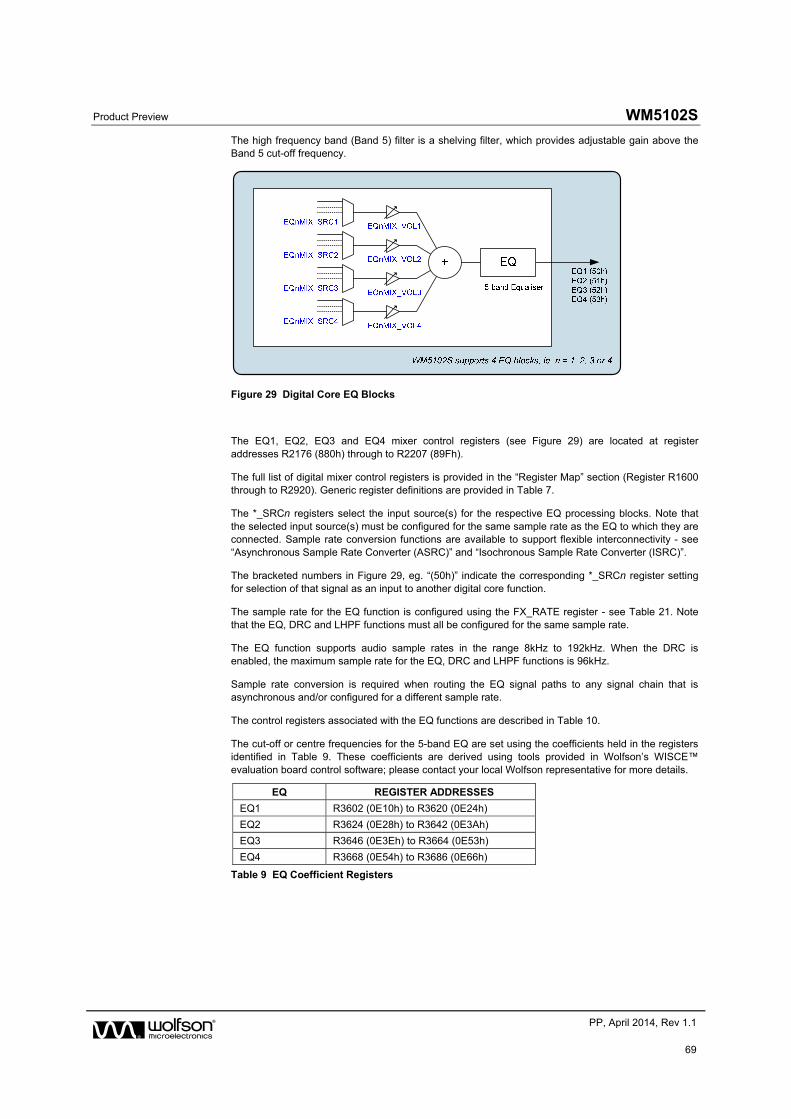
Product Preview WM5102S
w PP, April 2014, Rev 1.1
69
The high frequency band (Band 5) filter is a shelving filter, which provides adjustable gain above the Band 5 cut-off frequency.
Figure 29 Digital Core EQ Blocks
The EQ1, EQ2, EQ3 and EQ4 mixer control registers (see Figure 29) are located at register addresses R2176 (880h) through to R2207 (89Fh).
The full list of digital mixer control registers is provided in the “Register Map” section (Register R1600 through to R2920). Generic register definitions are provided in Table 7.
The *_SRCn registers select the input source(s) for the respective EQ processing blocks. Note that the selected input source(s) must be configured for the same sample rate as the EQ to which they are connected. Sample rate conversion functions are available to support flexible interconnectivity - see “Asynchronous Sample Rate Converter (ASRC)” and “Isochronous Sample Rate Converter (ISRC)”.
The bracketed numbers in Figure 29, eg. “(50h)” indicate the corresponding *_SRCn register setting for selection of that signal as an input to another digital core function.
The sample rate for the EQ function is configured using the FX_RATE register - see Table 21. Note that the EQ, DRC and LHPF functions must all be configured for the same sample rate.
The EQ function supports audio sample rates in the range 8kHz to 192kHz. When the DRC is enabled, the maximum sample rate for the EQ, DRC and LHPF functions is 96kHz.
Sample rate conversion is required when routing the EQ signal paths to any signal chain that is asynchronous and/or configured for a different sample rate.
The control registers associated with the EQ functions are described in Table 10.
The cut-off or centre frequencies for the 5-band EQ are set using the coefficients held in the registers identified in Table 9. These coefficients are derived using tools provided in Wolfson’s WISCE™ evaluation board control software; please contact your local Wolfson representative for more details.
EQ REGISTER ADDRESSES
EQ1 R3602 (0E10h) to R3620 (0E24h)
EQ2 R3624 (0E28h) to R3642 (0E3Ah)
EQ3 R3646 (0E3Eh) to R3664 (0E53h)
EQ4 R3668 (0E54h) to R3686 (0E66h)
Table 9 EQ Coefficient Registers
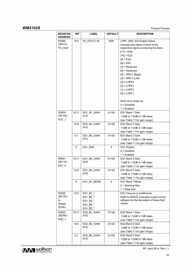
WM5102S Product Preview
w PP, April 2014, Rev 1.1
70
REGISTER ADDRESS
BIT LABEL DEFAULT DESCRIPTION
R3585 (0E01h)
FX_Ctrl2
15:4 FX_STS [11:0] 000h LHPF, DRC, EQ Enable Status
Indicates the status of each of the respective signal processing functions.
[11] = EQ4
[10] = EQ3
[9] = EQ2
[8] = EQ1
[7] = Reserved
[6] = Reserved
[5] = DRC1 (Right)
[4] = DRC1 (Left)
[3] = LHPF4
[2] = LHPF3
[1] = LHPF2
[0] = LHPF1
Each bit is coded as:
0 = Disabled
1 = Enabled
R3600 (0E10h)
EQ1_1
15:11 EQ1_B1_GAIN [4:0]
01100 EQ1 Band 1 Gain
-12dB to +12dB in 1dB steps
(see Table 11 for gain range)
10:6 EQ1_B2_GAIN [4:0]
01100 EQ1 Band 2 Gain
-12dB to +12dB in 1dB steps
(see Table 11 for gain range)
5:1 EQ1_B3_GAIN [4:0]
01100 EQ1 Band 3 Gain
-12dB to +12dB in 1dB steps
(see Table 11 for gain range)
0 EQ1_ENA 0 EQ1 Enable
0 = Disabled
1 = Enabled
R3601 (0E11h)
EQ1_2
15:11 EQ1_B4_GAIN [4:0]
01100 EQ1 Band 4 Gain
-12dB to +12dB in 1dB steps
(see Table 11 for gain range)
10:6 EQ1_B5_GAIN [4:0]
01100 EQ1 Band 5 Gain
-12dB to +12dB in 1dB steps
(see Table 11 for gain range)
0 EQ1_B1_MODE 0 EQ1 Band 1 Mode
0 = Shelving filter
1 = Peak filter
R3602 (0E12h)
to
R3620 (E24h)
15:0 EQ1_B1_*
EQ1_B2_*
EQ1_B3_*
EQ1_B4_*
EQ1_B5_*
EQ1 Frequency Coefficients
Refer to WISCE evaluation board control software for the deriviation of these field values.
R3622 (0E26h)
EQ2_1
15:11 EQ2_B1_GAIN [4:0]
01100 EQ2 Band 1 Gain
-12dB to +12dB in 1dB steps
(see Table 11 for gain range)
10:6 EQ2_B2_GAIN [4:0]
01100 EQ2 Band 2 Gain
-12dB to +12dB in 1dB steps
(see Table 11 for gain range)
5:1 EQ2_B3_GAIN [4:0]
01100 EQ2 Band 3 Gain
-12dB to +12dB in 1dB steps
(see Table 11 for gain range)
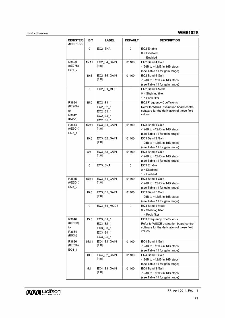
Product Preview WM5102S
w PP, April 2014, Rev 1.1
71
REGISTER ADDRESS
BIT LABEL DEFAULT DESCRIPTION
0 EQ2_ENA 0 EQ2 Enable
0 = Disabled
1 = Enabled
R3623 (0E27h)
EQ2_2
15:11 EQ2_B4_GAIN [4:0]
01100 EQ2 Band 4 Gain
-12dB to +12dB in 1dB steps
(see Table 11 for gain range)
10:6 EQ2_B5_GAIN [4:0]
01100 EQ2 Band 5 Gain
-12dB to +12dB in 1dB steps
(see Table 11 for gain range)
0 EQ2_B1_MODE 0 EQ2 Band 1 Mode
0 = Shelving filter
1 = Peak filter
R3624 (0E28h)
to
R3642 (E3Ah)
15:0 EQ2_B1_*
EQ2_B2_*
EQ2_B3_*
EQ2_B4_*
EQ2_B5_*
EQ2 Frequency Coefficients
Refer to WISCE evaluation board control software for the deriviation of these field values.
R3644 (0E3Ch)
EQ3_1
15:11 EQ3_B1_GAIN [4:0]
01100 EQ3 Band 1 Gain
-12dB to +12dB in 1dB steps
(see Table 11 for gain range)
10:6 EQ3_B2_GAIN [4:0]
01100 EQ3 Band 2 Gain
-12dB to +12dB in 1dB steps
(see Table 11 for gain range)
5:1 EQ3_B3_GAIN [4:0]
01100 EQ3 Band 3 Gain
-12dB to +12dB in 1dB steps
(see Table 11 for gain range)
0 EQ3_ENA 0 EQ3 Enable
0 = Disabled
1 = Enabled
R3645 (0E3Dh)
EQ3_2
15:11 EQ3_B4_GAIN [4:0]
01100 EQ3 Band 4 Gain
-12dB to +12dB in 1dB steps
(see Table 11 for gain range)
10:6 EQ3_B5_GAIN [4:0]
01100 EQ3 Band 5 Gain
-12dB to +12dB in 1dB steps
(see Table 11 for gain range)
0 EQ3_B1_MODE 0 EQ3 Band 1 Mode
0 = Shelving filter
1 = Peak filter
R3646 (0E3Eh)
to
R3664 (E50h)
15:0 EQ3_B1_*
EQ3_B2_*
EQ3_B3_*
EQ3_B4_*
EQ3_B5_*
EQ3 Frequency Coefficients
Refer to WISCE evaluation board control software for the deriviation of these field values.
R3666 (0E52h)
EQ4_1
15:11 EQ4_B1_GAIN [4:0]
01100 EQ4 Band 1 Gain
-12dB to +12dB in 1dB steps
(see Table 11 for gain range)
10:6 EQ4_B2_GAIN [4:0]
01100 EQ4 Band 2 Gain
-12dB to +12dB in 1dB steps
(see Table 11 for gain range)
5:1 EQ4_B3_GAIN [4:0]
01100 EQ4 Band 3 Gain
-12dB to +12dB in 1dB steps
(see Table 11 for gain range)
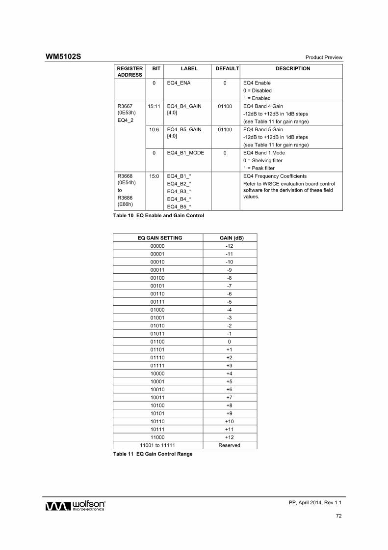
WM5102S Product Preview
w PP, April 2014, Rev 1.1
72
REGISTER ADDRESS
BIT LABEL DEFAULT DESCRIPTION
0 EQ4_ENA 0 EQ4 Enable
0 = Disabled
1 = Enabled
R3667 (0E53h)
EQ4_2
15:11 EQ4_B4_GAIN [4:0]
01100 EQ4 Band 4 Gain
-12dB to +12dB in 1dB steps
(see Table 11 for gain range)
10:6 EQ4_B5_GAIN [4:0]
01100 EQ4 Band 5 Gain
-12dB to +12dB in 1dB steps
(see Table 11 for gain range)
0 EQ4_B1_MODE 0 EQ4 Band 1 Mode
0 = Shelving filter
1 = Peak filter
R3668 (0E54h)
to
R3686 (E66h)
15:0 EQ4_B1_*
EQ4_B2_*
EQ4_B3_*
EQ4_B4_*
EQ4_B5_*
EQ4 Frequency Coefficients
Refer to WISCE evaluation board control software for the deriviation of these field values.
Table 10 EQ Enable and Gain Control
EQ GAIN SETTING GAIN (dB)
00000 -12
00001 -11
00010 -10
00011 -9
00100 -8
00101 -7
00110 -6
00111 -5
01000 -4
01001 -3
01010 -2
01011 -1
01100 0
01101 +1
01110 +2
01111 +3
10000 +4
10001 +5
10010 +6
10011 +7
10100 +8
10101 +9
10110 +10
10111 +11
11000 +12
11001 to 11111 Reserved
Table 11 EQ Gain Control Range
Product Preview WM5102S
w PP, April 2014, Rev 1.1
73
The WM5102S performs automatic checks to confirm that the SYSCLK frequency is high enough to support the commanded EQ and digital mixing functions. If an attempt is made to enable an EQ signal path, and there are insufficient SYSCLK cycles to support it, then the attempt will be unsuccessful. (Note that any signal paths that are already active will not be affected under these circumstances.)
The Underclocked Error can be monitored using the GPIO and/or Interrupt functions. See “General Purpose Input / Output” and “Interrupts” for further details.
The FX_STS field in Register R3585 indicates the status of each of the EQ, DRC and LHPF signal paths. If an Underclocked Error condition occurs, then this register provides readback of which EQ, DRC or LHPF signal path(s) have been successfully enabled.
The status bits in Registers R1600 to R2920 indicate the status of each of the digital mixers. If an Underclocked Error condition occurs, then these bits provide readback of which mixer(s) have been successfully enabled.
DYNAMIC RANGE CONTROL (DRC)
The digital core provides a stereo Dynamic Range Control (DRC) processing block as illustrated in Figure 30. A 4-input mixer is associated with each DRC input channel. The 4 input sources are selectable in each case, and independent volume control is provided for each path.
The function of the DRC is to adjust the signal gain in conditions where the input amplitude is unknown or varies over a wide range, e.g. when recording from microphones built into a handheld system, or to restrict the dynamic range of an output signal path.
The DRC can apply Compression and Automatic Level Control to the signal path. It incorporates ‘anti-clip’ and ‘quick release’ features for handling transients in order to improve intelligibility in the presence of loud impulsive noises.
The DRC also incorporates a Noise Gate function, which provides additional attenuation of very low-level input signals. This means that the signal path is quiet when no signal is present, giving an improvement in background noise level under these conditions.
A Signal Detect function is provided within the DRC; this can be used to detect the presence of an audio signal, and used to trigger other events. The Signal Detect function can be used as an Interrupt event, or as a GPIO output, or used to trigger the Control Write Sequencer.
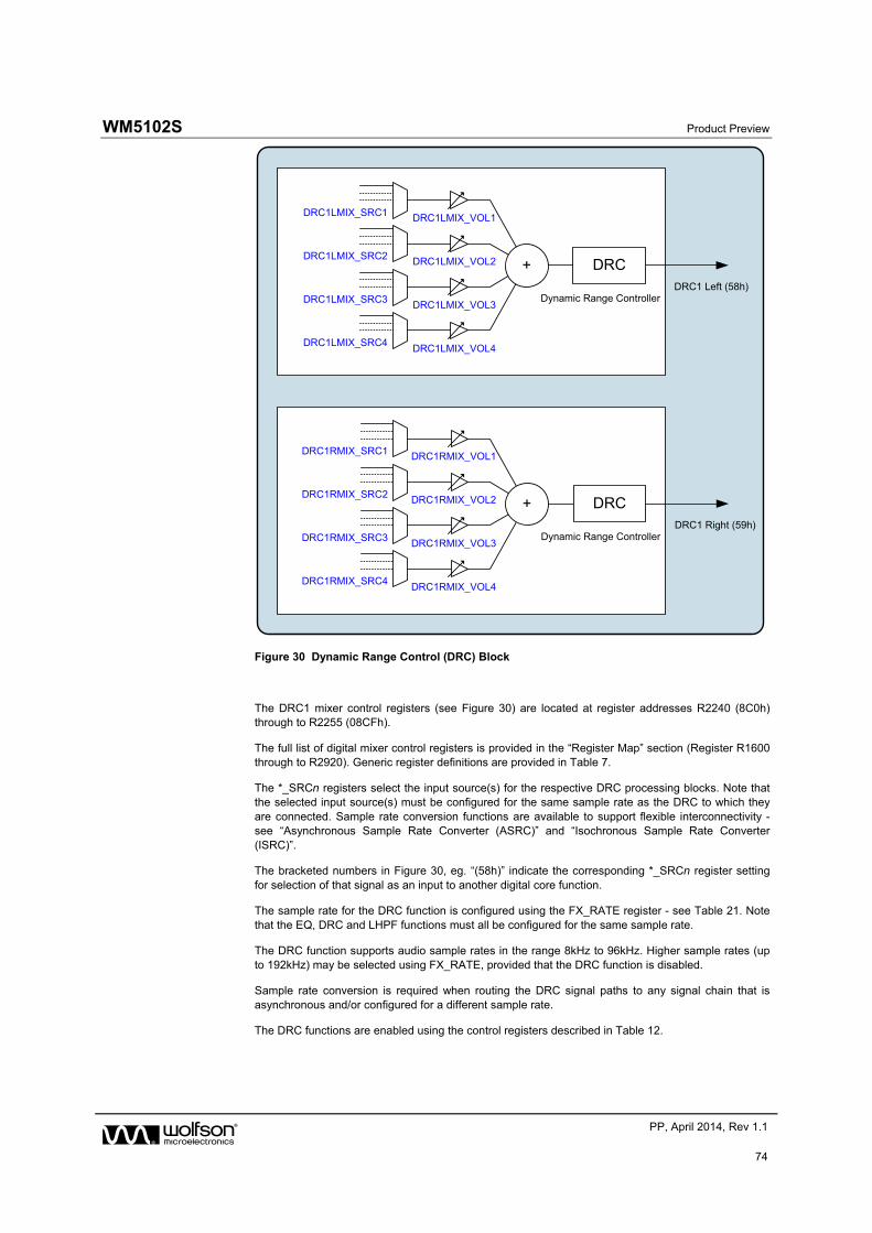
WM5102S Product Preview
w PP, April 2014, Rev 1.1
74
DRC1LMIX_VOL2
DRC1LMIX_VOL3
DRC1LMIX_VOL4
+
DRC1LMIX_VOL1DRC1LMIX_SRC1
DRC1LMIX_SRC3
DRC1LMIX_SRC4
DRC1LMIX_SRC2
DRC1 Left (58h)
DRC
Dynamic Range Controller
DRC1RMIX_VOL2
DRC1RMIX_VOL3
DRC1RMIX_VOL4
+
DRC1RMIX_VOL1DRC1RMIX_SRC1
DRC1RMIX_SRC3
DRC1RMIX_SRC4
DRC1RMIX_SRC2
DRC1 Right (59h)
DRC
Dynamic Range Controller
Figure 30 Dynamic Range Control (DRC) Block
The DRC1 mixer control registers (see Figure 30) are located at register addresses R2240 (8C0h) through to R2255 (08CFh).
The full list of digital mixer control registers is provided in the “Register Map” section (Register R1600 through to R2920). Generic register definitions are provided in Table 7.
The *_SRCn registers select the input source(s) for the respective DRC processing blocks. Note that the selected input source(s) must be configured for the same sample rate as the DRC to which they are connected. Sample rate conversion functions are available to support flexible interconnectivity - see “Asynchronous Sample Rate Converter (ASRC)” and “Isochronous Sample Rate Converter (ISRC)”.
The bracketed numbers in Figure 30, eg. “(58h)” indicate the corresponding *_SRCn register setting for selection of that signal as an input to another digital core function.
The sample rate for the DRC function is configured using the FX_RATE register - see Table 21. Note that the EQ, DRC and LHPF functions must all be configured for the same sample rate.
The DRC function supports audio sample rates in the range 8kHz to 96kHz. Higher sample rates (up to 192kHz) may be selected using FX_RATE, provided that the DRC function is disabled.
Sample rate conversion is required when routing the DRC signal paths to any signal chain that is asynchronous and/or configured for a different sample rate.
The DRC functions are enabled using the control registers described in Table 12.
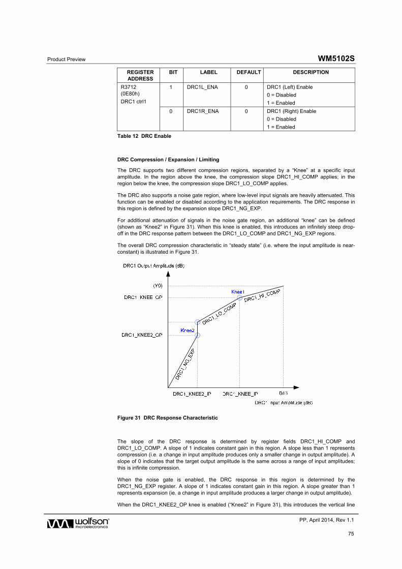
Product Preview WM5102S
w PP, April 2014, Rev 1.1
75
REGISTER ADDRESS
BIT LABEL DEFAULT DESCRIPTION
R3712 (0E80h)
DRC1 ctrl1
1 DRC1L_ENA 0 DRC1 (Left) Enable
0 = Disabled
1 = Enabled
0 DRC1R_ENA 0 DRC1 (Right) Enable
0 = Disabled
1 = Enabled
Table 12 DRC Enable
DRC Compression / Expansion / Limiting
The DRC supports two different compression regions, separated by a “Knee” at a specific input amplitude. In the region above the knee, the compression slope DRC1_HI_COMP applies; in the region below the knee, the compression slope DRC1_LO_COMP applies.
The DRC also supports a noise gate region, where low-level input signals are heavily attenuated. This function can be enabled or disabled according to the application requirements. The DRC response in this region is defined by the expansion slope DRC1_NG_EXP.
For additional attenuation of signals in the noise gate region, an additional “knee” can be defined (shown as “Knee2” in Figure 31). When this knee is enabled, this introduces an infinitely steep drop-off in the DRC response pattern between the DRC1_LO_COMP and DRC1_NG_EXP regions.
The overall DRC compression characteristic in “steady state” (i.e. where the input amplitude is near-constant) is illustrated in Figure 31.
Figure 31 DRC Response Characteristic
The slope of the DRC response is determined by register fields DRC1_HI_COMP and DRC1_LO_COMP. A slope of 1 indicates constant gain in this region. A slope less than 1 represents compression (i.e. a change in input amplitude produces only a smaller change in output amplitude). A slope of 0 indicates that the target output amplitude is the same across a range of input amplitudes; this is infinite compression.
When the noise gate is enabled, the DRC response in this region is determined by the DRC1_NG_EXP register. A slope of 1 indicates constant gain in this region. A slope greater than 1 represents expansion (ie. a change in input amplitude produces a larger change in output amplitude).
When the DRC1_KNEE2_OP knee is enabled (“Knee2” in Figure 31), this introduces the vertical line
WM5102S Product Preview
w PP, April 2014, Rev 1.1
76
in the response pattern illustrated, resulting in infinitely steep attenuation at this point in the response.
The DRC parameters are listed in Table 13.
REF PARAMETER DESCRIPTION
1 DRC1_KNEE_IP Input level at Knee1 (dB)
2 DRC1_KNEE_OP Output level at Knee2 (dB)
3 DRC1_HI_COMP Compression ratio above Knee1
4 DRC1_LO_COMP Compression ratio below Knee1
5 DRC1_KNEE2_IP Input level at Knee2 (dB)
6 DRC1_NG_EXP Expansion ratio below Knee2
7 DRC1_KNEE2_OP Output level at Knee2 (dB)
Table 13 DRC Response Parameters
The noise gate is enabled when the DRC1_NG_ENA register is set. When the noise gate is not enabled, parameters 5, 6, 7 above are ignored, and the DRC1_LO_COMP slope applies to all input signal levels below Knee1.
The DRC1_KNEE2_OP knee is enabled when the DRC1_KNEE2_OP_ENA register is set. When this bit is not set, then parameter 7 above is ignored, and the Knee2 position always coincides with the low end of the DRC1_LO_COMP region.
The “Knee1” point in Figure 31 is determined by register fields DRC1_KNEE_IP and DRC1_KNEE_OP.
Parameter Y0, the output level for a 0dB input, is not specified directly, but can be calculated from the other parameters, using the equation:
Y0 = DRC1_KNEE_OP - (DRC1_KNEE_IP x DRC1_HI_COMP)
Gain Limits
The minimum and maximum gain applied by the DRC is set by register fields DRC1_MINGAIN, DRC1_MAXGAIN and DRC1_NG_MINGAIN. These limits can be used to alter the DRC response from that illustrated in Figure 31. If the range between maximum and minimum gain is reduced, then the extent of the dynamic range control is reduced.
The minimum gain in the Compression regions of the DRC response is set by DRC1_MINGAIN. The mimimum gain in the Noise Gate region is set by DRC1_NG_MINGAIN. The minimum gain limit prevents excessive attenuation of the signal path.
The maximum gain limit set by DRC1_MAXGAIN prevents quiet signals (or silence) from being excessively amplified.
Dynamic Characteristics
The dynamic behaviour determines how quickly the DRC responds to changing signal levels. Note that the DRC responds to the average (RMS) signal amplitude over a period of time.
The DRC1_ATK determines how quickly the DRC gain decreases when the signal amplitude is high. The DRC1_DCY determines how quickly the DRC gain increases when the signal amplitude is low.
These register fields are described in Table 14. Note that the register defaults are suitable for general purpose microphone use.

Product Preview WM5102S
w PP, April 2014, Rev 1.1
77
Anti-Clip Control
The DRC includes an Anti-Clip feature to avoid signal clipping when the input amplitude rises very quickly. This feature uses a feed-forward technique for early detection of a rising signal level. Signal clipping is avoided by dynamically increasing the gain attack rate when required. The Anti-Clip feature is enabled using the DRC1_ANTICLIP bit.
Note that the feed-forward processing increases the latency in the input signal path.
Note that the Anti-Clip feature operates entirely in the digital domain. It cannot be used to prevent signal clipping in the analogue domain nor in the source signal. Analogue clipping can only be prevented by reducing the analogue signal gain or by adjusting the source signal.
Quick Release Control
The DRC includes a Quick-Release feature to handle short transient peaks that are not related to the intended source signal. For example, in handheld microphone recording, transient signal peaks sometimes occur due to user handling, key presses or accidental tapping against the microphone. The Quick Release feature ensures that these transients do not cause the intended signal to be masked by the longer time constant of DRC1_DCY.
The Quick-Release feature is enabled by setting the DRC1_QR bit. When this bit is enabled, the DRC measures the crest factor (peak to RMS ratio) of the input signal. A high crest factor is indicative of a transient peak that may not be related to the intended source signal. If the crest factor exceeds the level set by DRC1_QR_THR, then the normal decay rate (DRC1_DCY) is ignored and a faster decay rate (DRC1_QR_DCY) is used instead.
Signal Activity Detect
The DRC incorporates a configurable signal detect function, allowing the signal level at the DRC input to be monitored and to be used to trigger other events. This can be used to detect the presence of a microphone signal on an ADC or digital mic channel, or can be used to detect an audio signal received over the digital audio interface.
The DRC Signal Detect function is enabled by setting DRC1_SIG_DET register bit. (Note that DRC1 must also be enabled.) The detection threshold is either a Peak level (Crest Factor) or an RMS level, depending on the DRC1_SIG_DET_MODE register bit. When Peak level is selected, the threshold is determined by DRC1_SIG_DET_PK, which defines the applicable Crest Factor (Peak to RMS ratio) threshold. If RMS level is selected, then the threshold is set using DRC1_SIG_DET_RMS.
The DRC Signal Detect function is an input to the Interrupt control circuit and can be used to trigger an Interrupt event - see “Interrupts”.
The DRC Signal Detect signal can be output directly on a GPIO pin as an external indication of the Signal Detection. See “General Purpose Input / Output” to configure a GPIO pin for this function.
The Control Write Sequencer can be triggered by the DRC Signal Detect function. This is enabled using the DRC1_WSEQ_SIG_DET_ENA register bit. See “Control Write Sequencer” for further details.
WM5102S Product Preview
w PP, April 2014, Rev 1.1
78
GPIO Outputs from DRC
The Dynamic Range Control (DRC) circuit provides a number of status outputs, which can be output directly on a GPIO pin as an external indication of the DRC Status. See “General Purpose Input / Output” to configure a GPIO pin for these functions.
Each of the DRC status outputs is described below.
The DRC Signal Detect flag indicates that a signal is present on the respective signal path. The threshold level for signal detection is configurable using the register fields are described in Table 14.
The DRC Anti-Clip flag indicates that the DRC Anti-Clip function has been triggered. In this event, the DRC gain is decreasing in response to a rising signal level. The flag is asserted until the DRC gain stablises.
The DRC Decay flag indicates that the DRC gain is increasing in response to a low level signal input. The flag is asserted until the DRC gain stabilises.
The DRC Noise Gate flag indicates that the DRC Noise Gate function has been triggered, indicating that an idle condition has been detected in the signal path.
The DRC Quick Release flag indicates that the DRC Quick Release function has been triggered. In this event, the DRC gain is increasing rapidly following detection of a short transient peak. The flag is asserted until the DRC gain stabilises.
DRC Register Controls
The DRC control registers are described in Table 14.
REGISTER ADDRESS
BIT LABEL DEFAULT DESCRIPTION
R3585 (0E01h)
FX_Ctrl2
15:4 FX_STS [11:0] 000h LHPF, DRC, EQ Enable Status
Indicates the status of each of the respective signal processing functions.
[11] = EQ4
[10] = EQ3
[9] = EQ2
[8] = EQ1
[7] = Reserved
[6] = Reserved
[5] = DRC1 (Right)
[4] = DRC1 (Left)
[3] = LHPF4
[2] = LHPF3
[1] = LHPF2
[0] = LHPF1
Each bit is coded as:
0 = Disabled
1 = Enabled
R3712 (0E80h)
DRC1 ctrl1
15:11 DRC1_SIG_DET_RMS [4:0]
00h DRC1 Signal Detect RMS Threshold.
This is the RMS signal level for signal detect to be indicated when DRC1_SIG_DET_MODE=1.
00h = -30dB
01h = -31.5dB
…. (1.5dB steps)
1Eh = -75dB
1Fh = -76.5dB
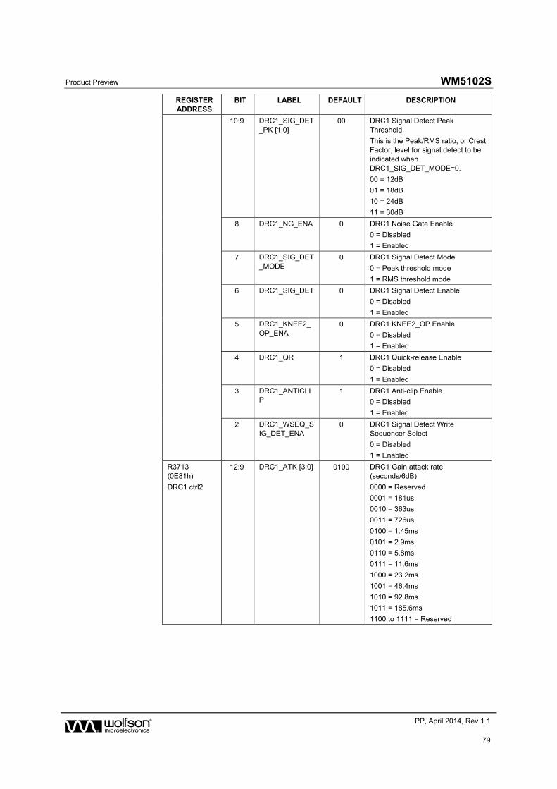
Product Preview WM5102S
w PP, April 2014, Rev 1.1
79
REGISTER ADDRESS
BIT LABEL DEFAULT DESCRIPTION
10:9 DRC1_SIG_DET_PK [1:0]
00 DRC1 Signal Detect Peak Threshold.
This is the Peak/RMS ratio, or Crest Factor, level for signal detect to be indicated when DRC1_SIG_DET_MODE=0.
00 = 12dB
01 = 18dB
10 = 24dB
11 = 30dB
8 DRC1_NG_ENA 0 DRC1 Noise Gate Enable
0 = Disabled
1 = Enabled
7 DRC1_SIG_DET_MODE
0 DRC1 Signal Detect Mode
0 = Peak threshold mode
1 = RMS threshold mode
6 DRC1_SIG_DET 0 DRC1 Signal Detect Enable
0 = Disabled
1 = Enabled
5 DRC1_KNEE2_OP_ENA
0 DRC1 KNEE2_OP Enable
0 = Disabled
1 = Enabled
4 DRC1_QR 1 DRC1 Quick-release Enable
0 = Disabled
1 = Enabled
3 DRC1_ANTICLIP
1 DRC1 Anti-clip Enable
0 = Disabled
1 = Enabled
2 DRC1_WSEQ_SIG_DET_ENA
0 DRC1 Signal Detect Write Sequencer Select
0 = Disabled
1 = Enabled
R3713 (0E81h)
DRC1 ctrl2
12:9 DRC1_ATK [3:0] 0100 DRC1 Gain attack rate (seconds/6dB)
0000 = Reserved
0001 = 181us
0010 = 363us
0011 = 726us
0100 = 1.45ms
0101 = 2.9ms
0110 = 5.8ms
0111 = 11.6ms
1000 = 23.2ms
1001 = 46.4ms
1010 = 92.8ms
1011 = 185.6ms
1100 to 1111 = Reserved
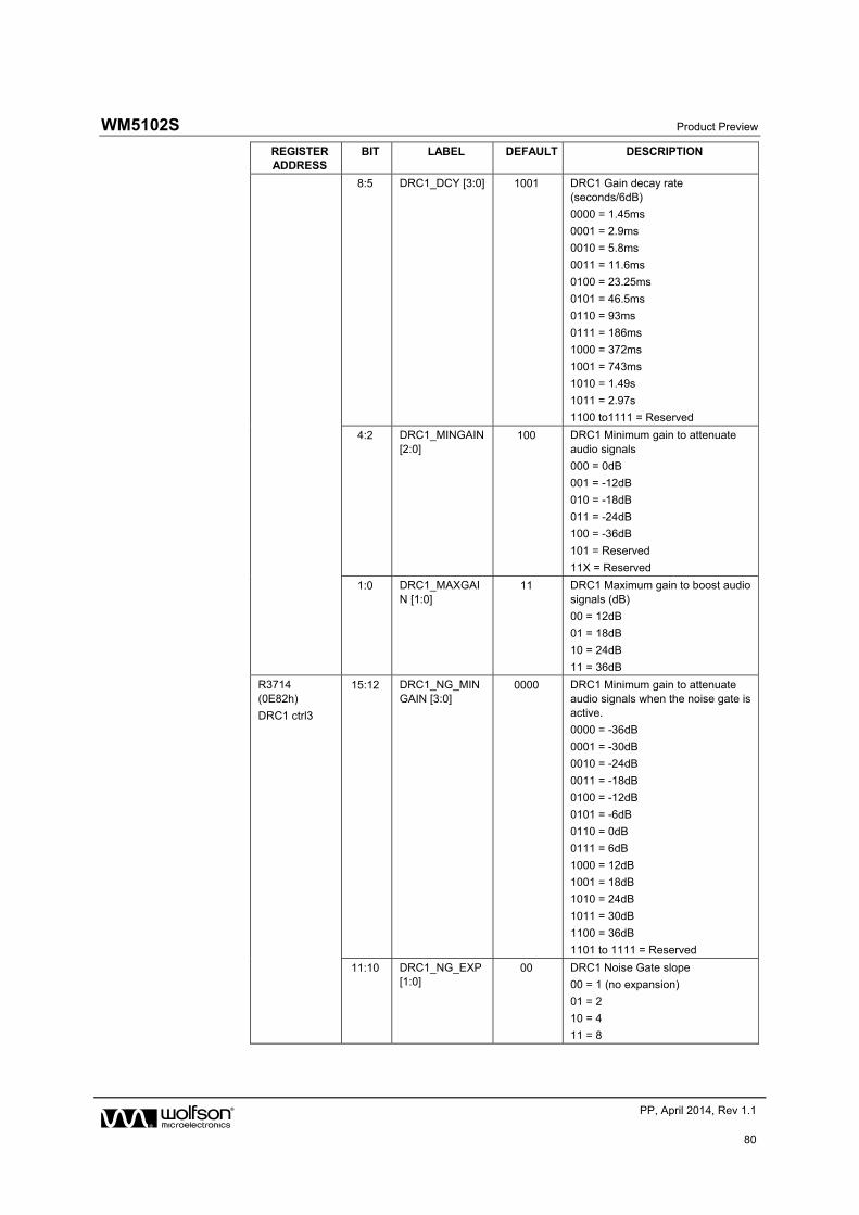
WM5102S Product Preview
w PP, April 2014, Rev 1.1
80
REGISTER ADDRESS
BIT LABEL DEFAULT DESCRIPTION
8:5 DRC1_DCY [3:0] 1001 DRC1 Gain decay rate (seconds/6dB)
0000 = 1.45ms
0001 = 2.9ms
0010 = 5.8ms
0011 = 11.6ms
0100 = 23.25ms
0101 = 46.5ms
0110 = 93ms
0111 = 186ms
1000 = 372ms
1001 = 743ms
1010 = 1.49s
1011 = 2.97s
1100 to1111 = Reserved
4:2 DRC1_MINGAIN [2:0]
100 DRC1 Minimum gain to attenuate audio signals
000 = 0dB
001 = -12dB
010 = -18dB
011 = -24dB
100 = -36dB
101 = Reserved
11X = Reserved
1:0 DRC1_MAXGAIN [1:0]
11 DRC1 Maximum gain to boost audio signals (dB)
00 = 12dB
01 = 18dB
10 = 24dB
11 = 36dB
R3714 (0E82h)
DRC1 ctrl3
15:12 DRC1_NG_MINGAIN [3:0]
0000 DRC1 Minimum gain to attenuate audio signals when the noise gate is active.
0000 = -36dB
0001 = -30dB
0010 = -24dB
0011 = -18dB
0100 = -12dB
0101 = -6dB
0110 = 0dB
0111 = 6dB
1000 = 12dB
1001 = 18dB
1010 = 24dB
1011 = 30dB
1100 = 36dB
1101 to 1111 = Reserved
11:10 DRC1_NG_EXP [1:0]
00 DRC1 Noise Gate slope
00 = 1 (no expansion)
01 = 2
10 = 4
11 = 8
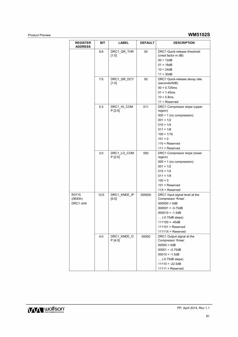
Product Preview WM5102S
w PP, April 2014, Rev 1.1
81
REGISTER ADDRESS
BIT LABEL DEFAULT DESCRIPTION
9:8 DRC1_QR_THR [1:0]
00 DRC1 Quick-release threshold (crest factor in dB)
00 = 12dB
01 = 18dB
10 = 24dB
11 = 30dB
7:6 DRC1_QR_DCY [1:0]
00 DRC1 Quick-release decay rate (seconds/6dB)
00 = 0.725ms
01 = 1.45ms
10 = 5.8ms
11 = Reserved
5:3 DRC1_HI_COMP [2:0]
011 DRC1 Compressor slope (upper region)
000 = 1 (no compression)
001 = 1/2
010 = 1/4
011 = 1/8
100 = 1/16
101 = 0
110 = Reserved
111 = Reserved
2:0 DRC1_LO_COMP [2:0]
000 DRC1 Compressor slope (lower region)
000 = 1 (no compression)
001 = 1/2
010 = 1/4
011 = 1/8
100 = 0
101 = Reserved
11X = Reserved
R3715 (0E83h)
DRC1 ctrl4
10:5 DRC1_KNEE_IP [5:0]
000000 DRC1 Input signal level at the Compressor ‘Knee’.
000000 = 0dB
000001 = -0.75dB
000010 = -1.5dB
… (-0.75dB steps)
111100 = -45dB
111101 = Reserved
11111X = Reserved
4:0 DRC1_KNEE_OP [4:0]
00000 DRC1 Output signal at the Compressor ‘Knee’.
00000 = 0dB
00001 = -0.75dB
00010 = -1.5dB
… (-0.75dB steps)
11110 = -22.5dB
11111 = Reserved
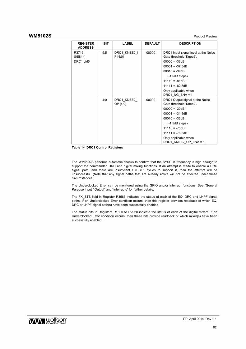
WM5102S Product Preview
w PP, April 2014, Rev 1.1
82
REGISTER ADDRESS
BIT LABEL DEFAULT DESCRIPTION
R3716 (0E84h)
DRC1 ctrl5
9:5 DRC1_KNEE2_IP [4:0]
00000 DRC1 Input signal level at the Noise Gate threshold ‘Knee2’.
00000 = -36dB
00001 = -37.5dB
00010 = -39dB
… (-1.5dB steps)
11110 = -81dB
11111 = -82.5dB
Only applicable when DRC1_NG_ENA = 1.
4:0 DRC1_KNEE2_OP [4:0]
00000 DRC1 Output signal at the Noise Gate threshold ‘Knee2’.
00000 = -30dB
00001 = -31.5dB
00010 = -33dB
… (-1.5dB steps)
11110 = -75dB
11111 = -76.5dB
Only applicable when DRC1_KNEE2_OP_ENA = 1.
Table 14 DRC1 Control Registers
The WM5102S performs automatic checks to confirm that the SYSCLK frequency is high enough to support the commanded DRC and digital mixing functions. If an attempt is made to enable a DRC signal path, and there are insufficient SYSCLK cycles to support it, then the attempt will be unsuccessful. (Note that any signal paths that are already active will not be affected under these circumstances.)
The Underclocked Error can be monitored using the GPIO and/or Interrupt functions. See “General Purpose Input / Output” and “Interrupts” for further details.
The FX_STS field in Register R3585 indicates the status of each of the EQ, DRC and LHPF signal paths. If an Underclocked Error condition occurs, then this register provides readback of which EQ, DRC or LHPF signal path(s) have been successfully enabled.
The status bits in Registers R1600 to R2920 indicate the status of each of the digital mixers. If an Underclocked Error condition occurs, then these bits provide readback of which mixer(s) have been successfully enabled.
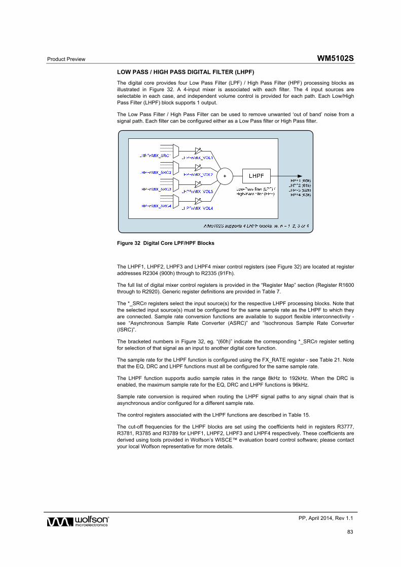
Product Preview WM5102S
w PP, April 2014, Rev 1.1
83
LOW PASS / HIGH PASS DIGITAL FILTER (LHPF)
The digital core provides four Low Pass Filter (LPF) / High Pass Filter (HPF) processing blocks as illustrated in Figure 32. A 4-input mixer is associated with each filter. The 4 input sources are selectable in each case, and independent volume control is provided for each path. Each Low/High Pass Filter (LHPF) block supports 1 output.
The Low Pass Filter / High Pass Filter can be used to remove unwanted ‘out of band’ noise from a signal path. Each filter can be configured either as a Low Pass filter or High Pass filter.
Figure 32 Digital Core LPF/HPF Blocks
The LHPF1, LHPF2, LHPF3 and LHPF4 mixer control registers (see Figure 32) are located at register addresses R2304 (900h) through to R2335 (91Fh).
The full list of digital mixer control registers is provided in the “Register Map” section (Register R1600 through to R2920). Generic register definitions are provided in Table 7.
The *_SRCn registers select the input source(s) for the respective LHPF processing blocks. Note that the selected input source(s) must be configured for the same sample rate as the LHPF to which they are connected. Sample rate conversion functions are available to support flexible interconnectivity - see “Asynchronous Sample Rate Converter (ASRC)” and “Isochronous Sample Rate Converter (ISRC)”.
The bracketed numbers in Figure 32, eg. “(60h)” indicate the corresponding *_SRCn register setting for selection of that signal as an input to another digital core function.
The sample rate for the LHPF function is configured using the FX_RATE register - see Table 21. Note that the EQ, DRC and LHPF functions must all be configured for the same sample rate.
The LHPF function supports audio sample rates in the range 8kHz to 192kHz. When the DRC is enabled, the maximum sample rate for the EQ, DRC and LHPF functions is 96kHz.
Sample rate conversion is required when routing the LHPF signal paths to any signal chain that is asynchronous and/or configured for a different sample rate.
The control registers associated with the LHPF functions are described in Table 15.
The cut-off frequencies for the LHPF blocks are set using the coefficients held in registers R3777, R3781, R3785 and R3789 for LHPF1, LHPF2, LHPF3 and LHPF4 respectively. These coefficients are derived using tools provided in Wolfson’s WISCE™ evaluation board control software; please contact your local Wolfson representative for more details.
WM5102S Product Preview
w PP, April 2014, Rev 1.1
84
REGISTER ADDRESS
BIT LABEL DEFAULT DESCRIPTION
R3585 (0E01h)
FX_Ctrl2
15:4 FX_STS [11:0] 000h LHPF, DRC, EQ Enable Status
Indicates the status of each of the respective signal processing functions.
[11] = EQ4
[10] = EQ3
[9] = EQ2
[8] = EQ1
[7] = Reserved
[6] = Reserved
[5] = DRC1 (Right)
[4] = DRC1 (Left)
[3] = LHPF4
[2] = LHPF3
[1] = LHPF2
[0] = LHPF1
Each bit is coded as:
0 = Disabled
1 = Enabled
R3776 (0EC0h)
HPLPF1_1
1 LHPF1_MODE 0 Low/High Pass Filter 1 Mode
0 = Low-Pass
1 = High-Pass
0 LHPF1_ENA 0 Low/High Pass Filter 1 Enable
0 = Disabled
1 = Enabled
R3777 (0EC1h)
HPLPF1_2
15:0 LHPF1_COEFF [15:0]
0000h Low/High Pass Filter 1 Frequency Coefficient
Refer to WISCE evaluation board control software for the derivation of this field value.
R3780 (0EC4h)
HPLPF2_1
1 LHPF2_MODE 0 Low/High Pass Filter 2 Mode
0 = Low-Pass
1 = High-Pass
0 LHPF2_ENA 0 Low/High Pass Filter 2 Enable
0 = Disabled
1 = Enabled
R3781 (0EC5h)
HPLPF2_2
15:0 LHPF2_COEFF [15:0]
0000h Low/High Pass Filter 2 Frequency Coefficient
Refer to WISCE evaluation board control software for the derivation of this field value.
R3784 (0EC8h)
HPLPF3_1
1 LHPF3_MODE 0 Low/High Pass Filter 3 Mode
0 = Low-Pass
1 = High-Pass
0 LHPF3_ENA 0 Low/High Pass Filter 3 Enable
0 = Disabled
1 = Enabled
R3785 (0EC9h)
HPLPF3_2
15:0 LHPF3_COEFF [15:0]
0000h Low/High Pass Filter 3 Frequency Coefficient
Refer to WISCE evaluation board control software for the derivation of this field value.
R3788 (0ECCh)
HPLPF4_
1 LHPF4_MODE 0 Low/High Pass Filter 4 Mode
0 = Low-Pass
1 = High-Pass
Product Preview WM5102S
w PP, April 2014, Rev 1.1
85
REGISTER ADDRESS
BIT LABEL DEFAULT DESCRIPTION
1 0 LHPF4_ENA 0 Low/High Pass Filter 4 Enable
0 = Disabled
1 = Enabled
R3789 (0ECDh)
HPLPF4_2
15:0 LHPF4_COEFF [15:0]
0000h Low/High Pass Filter 4 Frequency Coefficient
Refer to WISCE evaluation board control software for the derivation of this field value.
Table 15 Low Pass Filter / High Pass Filter Control
The WM5102S performs automatic checks to confirm that the SYSCLK frequency is high enough to support the commanded LHPF and digital mixing functions. If an attempt is made to enable an LHPF signal path, and there are insufficient SYSCLK cycles to support it, then the attempt will be unsuccessful. (Note that any signal paths that are already active will not be affected under these circumstances.)
The Underclocked Error can be monitored using the GPIO and/or Interrupt functions. See “General Purpose Input / Output” and “Interrupts” for further details.
The FX_STS field in Register R3585 indicates the status of each of the EQ, DRC and LHPF signal paths. If an Underclocked Error condition occurs, then this register provides readback of which EQ, DRC or LHPF signal path(s) have been successfully enabled.
The status bits in Registers R1600 to R2920 indicate the status of each of the digital mixers. If an Underclocked Error condition occurs, then these bits provide readback of which mixer(s) have been successfully enabled.
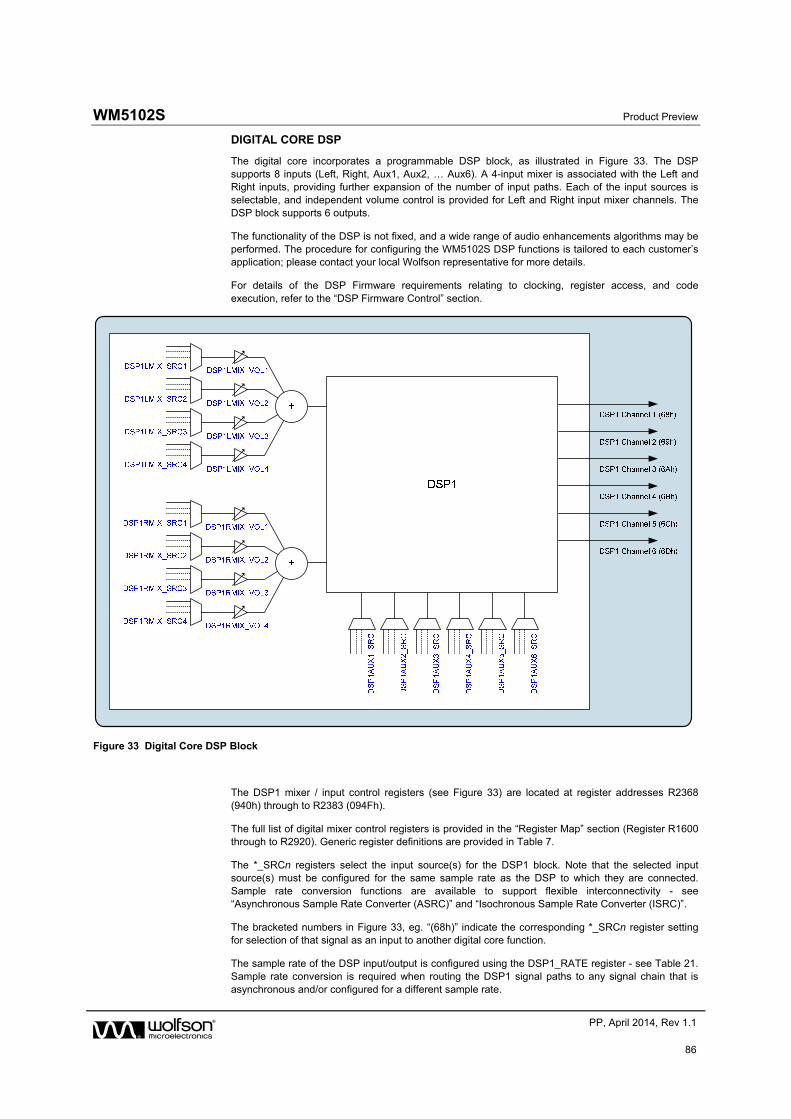
WM5102S Product Preview
w PP, April 2014, Rev 1.1
86
DIGITAL CORE DSP
The digital core incorporates a programmable DSP block, as illustrated in Figure 33. The DSP supports 8 inputs (Left, Right, Aux1, Aux2, … Aux6). A 4-input mixer is associated with the Left and Right inputs, providing further expansion of the number of input paths. Each of the input sources is selectable, and independent volume control is provided for Left and Right input mixer channels. The DSP block supports 6 outputs.
The functionality of the DSP is not fixed, and a wide range of audio enhancements algorithms may be performed. The procedure for configuring the WM5102S DSP functions is tailored to each customer’s application; please contact your local Wolfson representative for more details.
For details of the DSP Firmware requirements relating to clocking, register access, and code execution, refer to the “DSP Firmware Control” section.
Figure 33 Digital Core DSP Block
The DSP1 mixer / input control registers (see Figure 33) are located at register addresses R2368 (940h) through to R2383 (094Fh).
The full list of digital mixer control registers is provided in the “Register Map” section (Register R1600 through to R2920). Generic register definitions are provided in Table 7.
The *_SRCn registers select the input source(s) for the DSP1 block. Note that the selected input source(s) must be configured for the same sample rate as the DSP to which they are connected. Sample rate conversion functions are available to support flexible interconnectivity - see “Asynchronous Sample Rate Converter (ASRC)” and “Isochronous Sample Rate Converter (ISRC)”.
The bracketed numbers in Figure 33, eg. “(68h)” indicate the corresponding *_SRCn register setting for selection of that signal as an input to another digital core function.
The sample rate of the DSP input/output is configured using the DSP1_RATE register - see Table 21. Sample rate conversion is required when routing the DSP1 signal paths to any signal chain that is asynchronous and/or configured for a different sample rate.
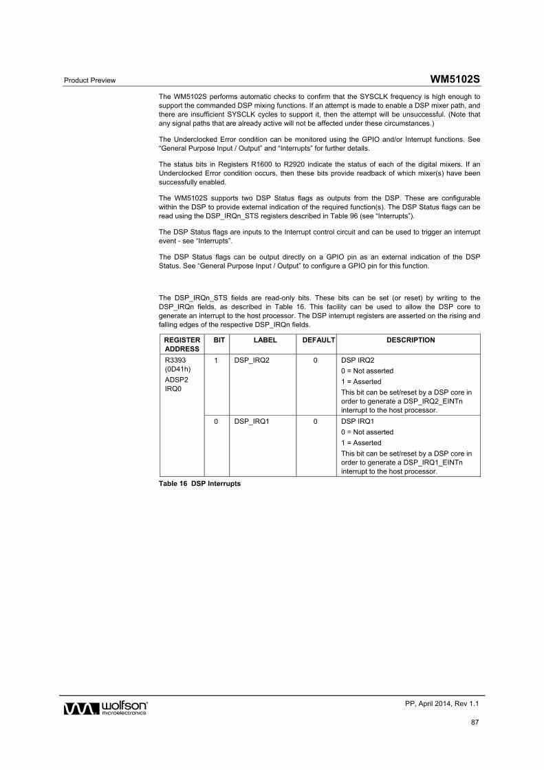
Product Preview WM5102S
w PP, April 2014, Rev 1.1
87
The WM5102S performs automatic checks to confirm that the SYSCLK frequency is high enough to support the commanded DSP mixing functions. If an attempt is made to enable a DSP mixer path, and there are insufficient SYSCLK cycles to support it, then the attempt will be unsuccessful. (Note that any signal paths that are already active will not be affected under these circumstances.)
The Underclocked Error condition can be monitored using the GPIO and/or Interrupt functions. See “General Purpose Input / Output” and “Interrupts” for further details.
The status bits in Registers R1600 to R2920 indicate the status of each of the digital mixers. If an Underclocked Error condition occurs, then these bits provide readback of which mixer(s) have been successfully enabled.
The WM5102S supports two DSP Status flags as outputs from the DSP. These are configurable within the DSP to provide external indication of the required function(s). The DSP Status flags can be read using the DSP_IRQn_STS registers described in Table 96 (see “Interrupts”).
The DSP Status flags are inputs to the Interrupt control circuit and can be used to trigger an interrupt event - see “Interrupts”.
The DSP Status flags can be output directly on a GPIO pin as an external indication of the DSP Status. See “General Purpose Input / Output” to configure a GPIO pin for this function.
The DSP_IRQn_STS fields are read-only bits. These bits can be set (or reset) by writing to the DSP_IRQn fields, as described in Table 16. This facility can be used to allow the DSP core to generate an interrupt to the host processor. The DSP interrupt registers are asserted on the rising and falling edges of the respective DSP_IRQn fields.
REGISTER ADDRESS
BIT LABEL DEFAULT DESCRIPTION
R3393 (0D41h)
ADSP2 IRQ0
1 DSP_IRQ2 0 DSP IRQ2
0 = Not asserted
1 = Asserted
This bit can be set/reset by a DSP core in order to generate a DSP_IRQ2_EINTn interrupt to the host processor.
0 DSP_IRQ1 0 DSP IRQ1
0 = Not asserted
1 = Asserted
This bit can be set/reset by a DSP core in order to generate a DSP_IRQ1_EINTn interrupt to the host processor.
Table 16 DSP Interrupts
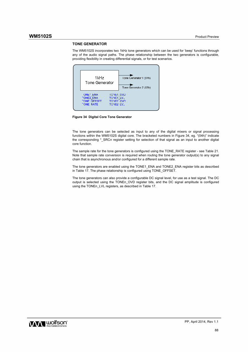
WM5102S Product Preview
w PP, April 2014, Rev 1.1
88
TONE GENERATOR
The WM5102S incorporates two 1kHz tone generators which can be used for ‘beep’ functions through any of the audio signal paths. The phase relationship between the two generators is configurable, providing flexibility in creating differential signals, or for test scenarios.
Figure 34 Digital Core Tone Generator
The tone generators can be selected as input to any of the digital mixers or signal processing functions within the WM5102S digital core. The bracketed numbers in Figure 34, eg. “(04h)” indicate the corresponding *_SRCn register setting for selection of that signal as an input to another digital core function.
The sample rate for the tone generators is configured using the TONE_RATE register - see Table 21. Note that sample rate conversion is required when routing the tone generator output(s) to any signal chain that is asynchronous and/or configured for a different sample rate.
The tone generators are enabled using the TONE1_ENA and TONE2_ENA register bits as described in Table 17. The phase relationship is configured using TONE_OFFSET.
The tone generators can also provide a configurable DC signal level, for use as a test signal. The DC output is selected using the TONEn_OVD register bits, and the DC signal amplitude is configured using the TONEn_LVL registers, as described in Table 17.
Product Preview WM5102S
w PP, April 2014, Rev 1.1
89
REGISTER ADDRESS
BIT LABEL DEFAULT DESCRIPTION
R32 (0020h)
Tone Generator 1
9:8 TONE_OFFSET [1:0]
00 Tone Generator Phase Offset
Sets the phase of Tone Generator 2 relative to Tone Generator 1
00 = 0 degrees (in phase)
01 = 90 degrees ahead
10 = 180 degrees ahead
11 = 270 degrees ahead
5 TONE2_OVD 0 Tone Generator 2 Override
0 = Disabled (1kHz tone output)
1 = Enabled (DC signal output)
The DC signal level, when selected, is configured using TONE2_LVL[23:0]
4 TONE1_OVD 0 Tone Generator 1 Override
0 = Disabled (1kHz tone output)
1 = Enabled (DC signal output)
The DC signal level, when selected, is configured using TONE1_LVL[23:0]
1 TONE2_ENA 0 Tone Generator 2 Enable
0 = Disabled
1 = Enabled
0 TONE1_ENA 0 Tone Generator 1 Enable
0 = Disabled
1 = Enabled
R33 (0021h)
Tone Generator 2
15:0 TONE1_LVL [23:8]
1000h Tone Generator 1 DC output level
TONE1_LVL [23:8] is coded as 2’s complement. Bits [23:20] contain the integer portion; bits [19:0] contain the fractional portion.
The digital core 0dBFS level corresponds to 1000_00h (+1) or F000_00h (-1).
R34 (0022h)
Tone Generator 3
7:0 TONE1_LVL [7:0] 00h Tone Generator 1 DC output level
TONE1_LVL [23:8] is coded as 2’s complement. Bits [23:20] contain the integer portion; bits [19:0] contain the fractional portion.
The digital core 0dBFS level corresponds to 1000_00h (+1) or F000_00h (-1).
R35 (0023h)
Tone Generator 4
15:0 TONE2_LVL [23:8]
1000h Tone Generator 2 DC output level
TONE2_LVL [23:8] is coded as 2’s complement. Bits [23:20] contain the integer portion; bits [19:0] contain the fractional portion.
The digital core 0dBFS level corresponds to 1000_00h (+1) or F000_00h (-1).
R36 (0024h)
Tone Generator 5
7:0 TONE2_LVL [7:0] 00h Tone Generator 2 DC output level
TONE2_LVL [23:8] is coded as 2’s complement. Bits [23:20] contain the integer portion; bits [19:0] contain the fractional portion.
The digital core 0dBFS level corresponds to 1000_00h (+1) or F000_00h (-1).
Table 17 Tone Generator Control
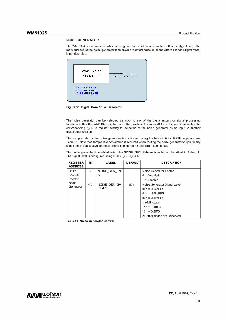
WM5102S Product Preview
w PP, April 2014, Rev 1.1
90
NOISE GENERATOR
The WM5102S incorporates a white noise generator, which can be routed within the digital core. The main purpose of the noise generator is to provide ‘comfort noise’ in cases where silence (digital mute) is not desirable.
Figure 35 Digital Core Noise Generator
The noise generator can be selected as input to any of the digital mixers or signal processing functions within the WM5102S digital core. The bracketed number (0Dh) in Figure 35 indicates the corresponding *_SRCn register setting for selection of the noise generator as an input to another digital core function.
The sample rate for the noise generator is configured using the NOISE_GEN_RATE register - see Table 21. Note that sample rate conversion is required when routing the noise generator output to any signal chain that is asynchronous and/or configured for a different sample rate.
The noise generator is enabled using the NOISE_GEN_ENA register bit as described in Table 18. The signal level is configured using NOISE_GEN_GAIN.
REGISTER ADDRESS
BIT LABEL DEFAULT DESCRIPTION
R112 (0070h)
Comfort Noise Generator
5 NOISE_GEN_ENA
0 Noise Generator Enable
0 = Disabled
1 = Enabled
4:0 NOISE_GEN_GAIN [4:0]
00h Noise Generator Signal Level
00h = -114dBFS
01h = -108dBFS
02h = -102dBFS
…(6dB steps)
11h = -6dBFS
12h = 0dBFS
All other codes are Reserved
Table 18 Noise Generator Control
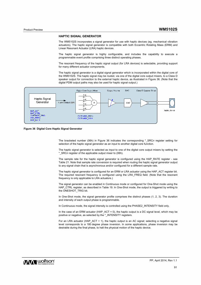
Product Preview WM5102S
w PP, April 2014, Rev 1.1
91
HAPTIC SIGNAL GENERATOR
The WM5102S incorporates a signal generator for use with haptic devices (eg. mechanical vibration actuators). The haptic signal generator is compatible with both Eccentric Rotating Mass (ERM) and Linear Resonant Actuator (LRA) haptic devices.
The haptic signal generator is highly configurable, and includes the capability to execute a programmable event profile comprising three distinct operating phases.
The resonant frequency of the haptic signal output (for LRA devices) is selectable, providing support for many different actuator components.
The haptic signal generator is a digital signal generator which is incorporated within the digital core of the WM5102S. The haptic signal may be routed, via one of the digital core output mixers, to a Class D speaker output for connection to the external haptic device, as illustrated in Figure 36. (Note that the digital PDM output paths may also be used for haptic signal output.)
Figure 36 Digital Core Haptic Signal Generator
The bracketed number (06h) in Figure 36 indicates the corresponding *_SRCn register setting for selection of the haptic signal generator as an input to another digital core function.
The haptic signal generator is selected as input to one of the digital core output mixers by setting the *_SRCn register of the applicable output mixer to (06h).
The sample rate for the haptic signal generator is configured using the HAP_RATE register - see Table 21. Note that sample rate conversion is required when routing the haptic signal generator output to any signal chain that is asynchronous and/or configured for a different sample rate.
The haptic signal generator is configured for an ERM or LRA actuator using the HAP_ACT register bit. The required resonant frequency is configured using the LRA_FREQ field. (Note that the resonant frequency is only applicable to LRA actuators.)
The signal generator can be enabled in Continuous mode or configured for One-Shot mode using the HAP_CTRL register, as described in Table 19. In One-Shot mode, the output is triggered by writing to the ONESHOT_TRIG bit.
In One-Shot mode, the signal generator profile comprises the distinct phases (1, 2, 3). The duration and intensity of each output phase is programmable.
In Continuous mode, the signal intensity is controlled using the PHASE2_INTENSITY field only.
In the case of an ERM actuator (HAP_ACT = 0), the haptic output is a DC signal level, which may be positive or negative, as selected by the *_INTENSITY registers.
For an LRA actuator (HAP_ACT = 1), the haptic output is an AC signal; selecting a negative signal level corresponds to a 180 degree phase inversion. In some applications, phase inversion may be desirable during the final phase, to halt the physical motion of the haptic device.
WM5102S Product Preview
w PP, April 2014, Rev 1.1
92
REGISTER ADDRESS
BIT LABEL DEFAULT DESCRIPTION
R144 (0090h)
Haptics Control 1
4 ONESHOT_TRIG 0 Haptic One-Shot Trigger
Writing ‘1’ starts the one-shot profile (ie. Phase 1, Phase 2, Phase 3)
3:2 HAP_CTRL [1:0] 00 Haptic Signal Generator Control
00 = Disabled
01 = Continuous
10 = One-Shot
11 = Reserved
1 HAP_ACT 0 Haptic Actuator Select
0 = Eccentric Rotating Mass (ERM)
1 = Linear Resonant Actuator (LRA)
R145 (0091h)
Haptics Control 2
14:0 LRA_FREQ [14:0] 7FFFh Haptic Resonant Frequency
Selects the haptic signal frequency (LRA actuator only, HAP_ACT = 1)
Haptic Frequency (Hz) =
System Clock / (2 x (LRA_FREQ+1))
where System Clock = 6.144MHz or 5.6448MHz, derived by division from SYSCLK or ASYNCCLK.
If HAP_RATE<1000, then SYSCLK is the clock source, and the applicable System Clock frequency is determined by SYSCLK.
If HAP_RATE>=1000, then ASYNCCLK is the clock source, and the applicable System Clock frequency is determined by ASYNCCLK.
Valid for Haptic Frequency in the range 100Hz to 250Hz
For 6.144MHz System Clock:
77FFh = 100Hz
4491h = 175Hz
2FFFh = 250Hz
For 5.6448MHz System Clock:
6E3Fh = 100Hz
3EFFh = 175Hz
2C18h = 250Hz
R146 (0092h)
Haptics phase 1 intensity
7:0 PHASE1_INTENSITY [7:0]
00h Haptic Output Level (Phase 1)
Selects the signal intensity of Phase 1 in one-shot mode.
Coded as 2’s complement.
Range is +/- Full Scale (FS).
For ERM actuator, this selects the DC signal level for the haptic output.
For LRA actuator, this selects the AC peak amplitude; Negative values correspond to a 180 degree phase shift.
Product Preview WM5102S
w PP, April 2014, Rev 1.1
93
REGISTER ADDRESS
BIT LABEL DEFAULT DESCRIPTION
R147 (0093h)
Haptics Control phase 1 duration
8:0 PHASE1_DURATION [8:0]
000h Haptic Output Duration (Phase 1)
Selects the duration of Phase 1 in one-shot mode.
000h = 0ms
001h = 0.625ms
002h = 1.25ms
… (0.625ms steps)
1FFh = 319.375ms
R148 (0094h)
Haptics phase 2 intensity
7:0 PHASE2_INTENSITY [7:0]
00h Haptic Output Level (Phase 2)
Selects the signal intensity in Continuous mode or Phase 2 of one-shot mode.
Coded as 2’s complement.
Range is +/- Full Scale (FS).
For ERM actuator, this selects the DC signal level for the haptic output.
For LRA actuator, this selects the AC peak amplitude; Negative values correspond to a 180 degree phase shift.
R149 (0095h)
Haptics phase 2 duration
10:0 PHASE2_DURATION [10:0]
000h Haptic Output Duration (Phase 2)
Selects the duration of Phase 2 in one-shot mode.
000h = 0ms
001h = 0.625ms
002h = 1.25ms
… (0.625ms steps)
7FFh = 1279.375ms
R150 (0096h)
Haptics phase 3 intensity
7:0 PHASE3_INTENSITY [7:0]
00h Haptic Output Level (Phase 3)
Selects the signal intensity of Phase 3 in one-shot mode.
Coded as 2’s complement.
Range is +/- Full Scale (FS).
For ERM actuator, this selects the DC signal level for the haptic output.
For LRA actuator, this selects the AC peak amplitude; Negative values correspond to a 180 degree phase shift.
R151 (0097h)
Haptics phase 3 duration
8:0 PHASE3_DURATION [8:0]
000h Haptic Output Duration (Phase 3)
Selects the duration of Phase 3 in one-shot mode.
000h = 0ms
001h = 0.625ms
002h = 1.25ms
… (0.625ms steps)
1FFh = 319.375ms
R152 (0098h)
Haptics Status
0 ONESHOT_STS 0 Haptic One-Shot status
0 = One-Shot event not in progress
1 = One-Shot event in progress
Table 19 Haptic Signal Generator Control
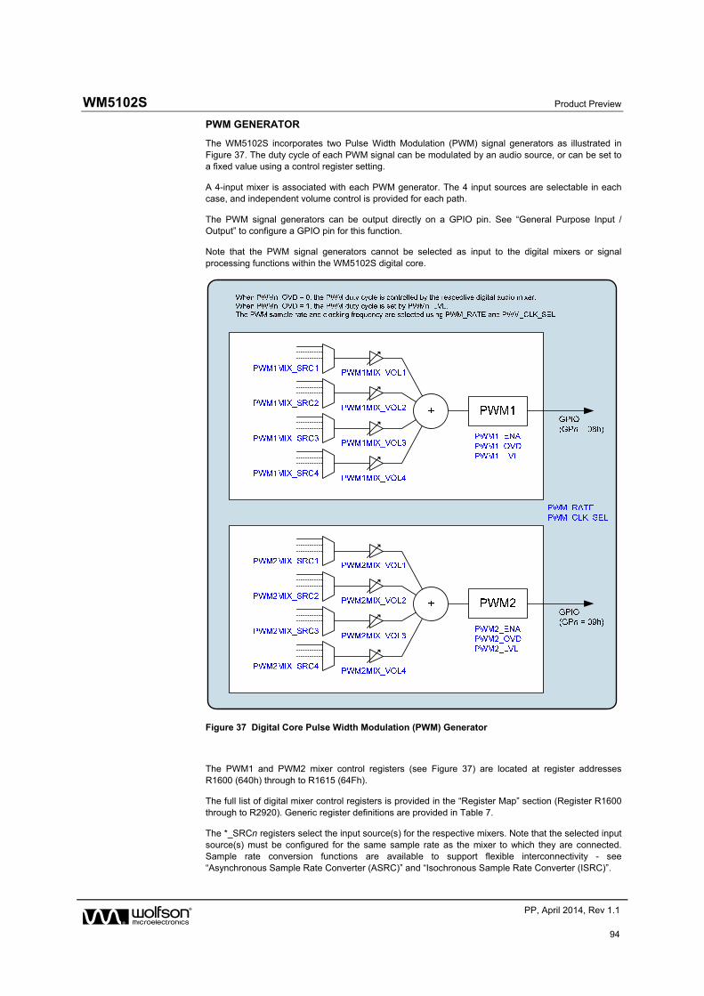
WM5102S Product Preview
w PP, April 2014, Rev 1.1
94
PWM GENERATOR
The WM5102S incorporates two Pulse Width Modulation (PWM) signal generators as illustrated in Figure 37. The duty cycle of each PWM signal can be modulated by an audio source, or can be set to a fixed value using a control register setting.
A 4-input mixer is associated with each PWM generator. The 4 input sources are selectable in each case, and independent volume control is provided for each path.
The PWM signal generators can be output directly on a GPIO pin. See “General Purpose Input / Output” to configure a GPIO pin for this function.
Note that the PWM signal generators cannot be selected as input to the digital mixers or signal processing functions within the WM5102S digital core.
Figure 37 Digital Core Pulse Width Modulation (PWM) Generator
The PWM1 and PWM2 mixer control registers (see Figure 37) are located at register addresses R1600 (640h) through to R1615 (64Fh).
The full list of digital mixer control registers is provided in the “Register Map” section (Register R1600 through to R2920). Generic register definitions are provided in Table 7.
The *_SRCn registers select the input source(s) for the respective mixers. Note that the selected input source(s) must be configured for the same sample rate as the mixer to which they are connected. Sample rate conversion functions are available to support flexible interconnectivity - see “Asynchronous Sample Rate Converter (ASRC)” and “Isochronous Sample Rate Converter (ISRC)”.
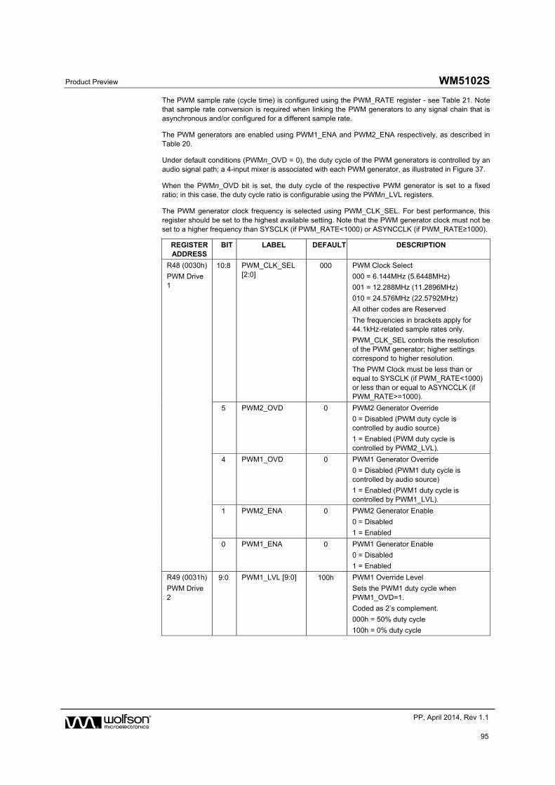
Product Preview WM5102S
w PP, April 2014, Rev 1.1
95
The PWM sample rate (cycle time) is configured using the PWM_RATE register - see Table 21. Note that sample rate conversion is required when linking the PWM generators to any signal chain that is asynchronous and/or configured for a different sample rate.
The PWM generators are enabled using PWM1_ENA and PWM2_ENA respectively, as described in Table 20.
Under default conditions (PWMn_OVD = 0), the duty cycle of the PWM generators is controlled by an audio signal path; a 4-input mixer is associated with each PWM generator, as illustrated in Figure 37.
When the PWMn_OVD bit is set, the duty cycle of the respective PWM generator is set to a fixed ratio; in this case, the duty cycle ratio is configurable using the PWMn_LVL registers.
The PWM generator clock frequency is selected using PWM_CLK_SEL. For best performance, this register should be set to the highest available setting. Note that the PWM generator clock must not be set to a higher frequency than SYSCLK (if PWM_RATE<1000) or ASYNCCLK (if PWM_RATE≥1000).
REGISTER ADDRESS
BIT LABEL DEFAULT DESCRIPTION
R48 (0030h)
PWM Drive 1
10:8 PWM_CLK_SEL [2:0]
000 PWM Clock Select
000 = 6.144MHz (5.6448MHz)
001 = 12.288MHz (11.2896MHz)
010 = 24.576MHz (22.5792MHz)
All other codes are Reserved
The frequencies in brackets apply for 44.1kHz-related sample rates only.
PWM_CLK_SEL controls the resolution of the PWM generator; higher settings correspond to higher resolution.
The PWM Clock must be less than or equal to SYSCLK (if PWM_RATE<1000) or less than or equal to ASYNCCLK (if PWM_RATE>=1000).
5 PWM2_OVD 0 PWM2 Generator Override
0 = Disabled (PWM duty cycle is controlled by audio source)
1 = Enabled (PWM duty cycle is controlled by PWM2_LVL).
4 PWM1_OVD 0 PWM1 Generator Override
0 = Disabled (PWM1 duty cycle is controlled by audio source)
1 = Enabled (PWM1 duty cycle is controlled by PWM1_LVL).
1 PWM2_ENA 0 PWM2 Generator Enable
0 = Disabled
1 = Enabled
0 PWM1_ENA 0 PWM1 Generator Enable
0 = Disabled
1 = Enabled
R49 (0031h)
PWM Drive 2
9:0 PWM1_LVL [9:0] 100h PWM1 Override Level
Sets the PWM1 duty cycle when PWM1_OVD=1.
Coded as 2’s complement.
000h = 50% duty cycle
100h = 0% duty cycle
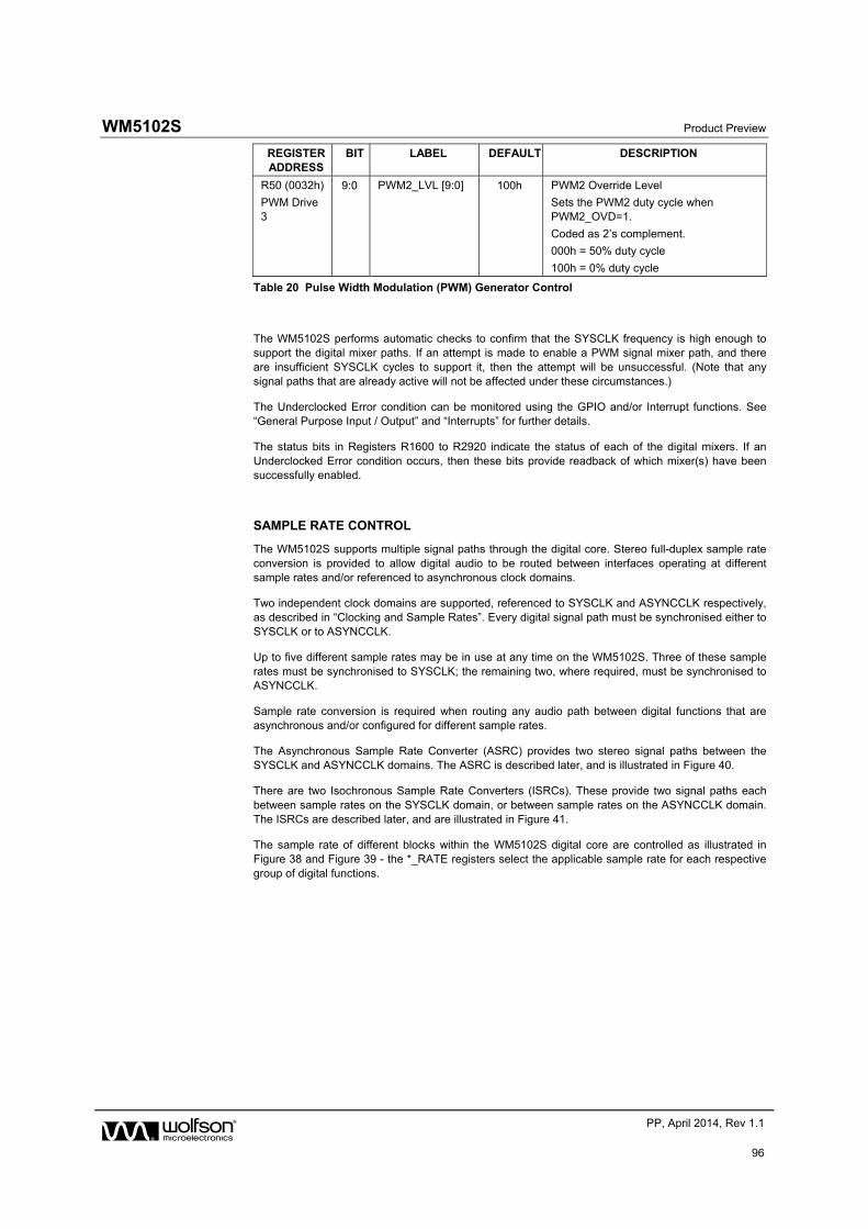
WM5102S Product Preview
w PP, April 2014, Rev 1.1
96
REGISTER ADDRESS
BIT LABEL DEFAULT DESCRIPTION
R50 (0032h)
PWM Drive 3
9:0 PWM2_LVL [9:0] 100h PWM2 Override Level
Sets the PWM2 duty cycle when PWM2_OVD=1.
Coded as 2’s complement.
000h = 50% duty cycle
100h = 0% duty cycle
Table 20 Pulse Width Modulation (PWM) Generator Control
The WM5102S performs automatic checks to confirm that the SYSCLK frequency is high enough to support the digital mixer paths. If an attempt is made to enable a PWM signal mixer path, and there are insufficient SYSCLK cycles to support it, then the attempt will be unsuccessful. (Note that any signal paths that are already active will not be affected under these circumstances.)
The Underclocked Error condition can be monitored using the GPIO and/or Interrupt functions. See “General Purpose Input / Output” and “Interrupts” for further details.
The status bits in Registers R1600 to R2920 indicate the status of each of the digital mixers. If an Underclocked Error condition occurs, then these bits provide readback of which mixer(s) have been successfully enabled.
SAMPLE RATE CONTROL
The WM5102S supports multiple signal paths through the digital core. Stereo full-duplex sample rate conversion is provided to allow digital audio to be routed between interfaces operating at different sample rates and/or referenced to asynchronous clock domains.
Two independent clock domains are supported, referenced to SYSCLK and ASYNCCLK respectively, as described in “Clocking and Sample Rates”. Every digital signal path must be synchronised either to SYSCLK or to ASYNCCLK.
Up to five different sample rates may be in use at any time on the WM5102S. Three of these sample rates must be synchronised to SYSCLK; the remaining two, where required, must be synchronised to ASYNCCLK.
Sample rate conversion is required when routing any audio path between digital functions that are asynchronous and/or configured for different sample rates.
The Asynchronous Sample Rate Converter (ASRC) provides two stereo signal paths between the SYSCLK and ASYNCCLK domains. The ASRC is described later, and is illustrated in Figure 40.
There are two Isochronous Sample Rate Converters (ISRCs). These provide two signal paths each between sample rates on the SYSCLK domain, or between sample rates on the ASYNCCLK domain. The ISRCs are described later, and are illustrated in Figure 41.
The sample rate of different blocks within the WM5102S digital core are controlled as illustrated in Figure 38 and Figure 39 - the *_RATE registers select the applicable sample rate for each respective group of digital functions.
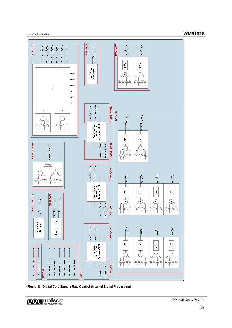
Product Preview WM5102S
w PP, April 2014, Rev 1.1
97
Figure 38 Digital Core Sample Rate Control (Internal Signal Processing)
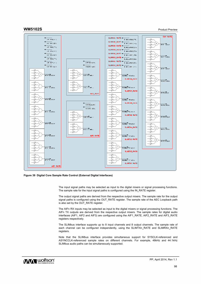
WM5102S Product Preview
w PP, April 2014, Rev 1.1
98
Figure 39 Digital Core Sample Rate Control (External Digital Interfaces)
The input signal paths may be selected as input to the digital mixers or signal processing functions. The sample rate for the input signal paths is configured using the IN_RATE register.
The output signal paths are derived from the respective output mixers. The sample rate for the output signal paths is configured using the OUT_RATE register. The sample rate of the AEC Loopback path is also set by the OUT_RATE register.
The AIFn RX inputs may be selected as input to the digital mixers or signal processing functions. The AIFn TX outputs are derived from the respective output mixers. The sample rates for digital audio interfaces (AIF1, AIF2 and AIF3) are configured using the AIF1_RATE, AIF2_RATE and AIF3_RATE registers respectively.
The SLIMbus interface supports up to 8 input channels and 8 output channels. The sample rate of each channel can be configured independently, using the SLIMTXn_RATE and SLIMRXn_RATE registers.
Note that the SLIMbus interface provides simultaneous support for SYSCLK-referenced and ASYNCCLK-referenced sample rates on different channels. For example, 48kHz and 44.1kHz SLIMbus audio paths can be simultaneously supported.
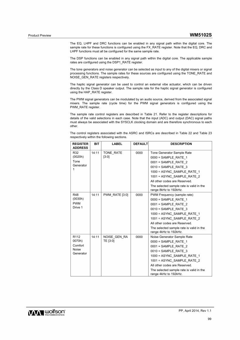
Product Preview WM5102S
w PP, April 2014, Rev 1.1
99
The EQ, LHPF and DRC functions can be enabled in any signal path within the digital core. The sample rate for these functions is configured using the FX_RATE register. Note that the EQ, DRC and LHPF functions must all be configured for the same sample rate.
The DSP functions can be enabled in any signal path within the digital core. The applicable sample rates are configured using the DSP1_RATE register.
The tone generators and noise generator can be selected as input to any of the digital mixers or signal processing functions. The sample rates for these sources are configured using the TONE_RATE and NOISE_GEN_RATE registers respectively.
The haptic signal generator can be used to control an external vibe actuator, which can be driven directly by the Class D speaker output. The sample rate for the haptic signal generator is configured using the HAP_RATE register.
The PWM signal generators can be modulated by an audio source, derived from the associated signal mixers. The sample rate (cycle time) for the PWM signal generators is configured using the PWM_RATE register.
The sample rate control registers are described in Table 21. Refer to the register descriptions for details of the valid selections in each case. Note that the input (ADC) and output (DAC) signal paths must always be associated with the SYSCLK clocking domain and are therefore synchronous to each other.
The control registers associated with the ASRC and ISRCs are described in Table 22 and Table 23 respectively within the following sections.
REGISTER ADDRESS
BIT LABEL DEFAULT DESCRIPTION
R32 (0020h)
Tone Generator 1
14:11 TONE_RATE [3:0]
0000 Tone Generator Sample Rate
0000 = SAMPLE_RATE_1
0001 = SAMPLE_RATE_2
0010 = SAMPLE_RATE_3
1000 = ASYNC_SAMPLE_RATE_1
1001 = ASYNC_SAMPLE_RATE_2
All other codes are Reserved.
The selected sample rate is valid in the range 8kHz to 192kHz.
R48 (0030h)
PWM Drive 1
14:11 PWM_RATE [3:0] 0000 PWM Frequency (sample rate)
0000 = SAMPLE_RATE_1
0001 = SAMPLE_RATE_2
0010 = SAMPLE_RATE_3
1000 = ASYNC_SAMPLE_RATE_1
1001 = ASYNC_SAMPLE_RATE_2
All other codes are Reserved.
The selected sample rate is valid in the range 4kHz to 192kHz.
R112 0070h)
Comfort Noise Generator
14:11 NOISE_GEN_RATE [3:0]
0000 Noise Generator Sample Rate
0000 = SAMPLE_RATE_1
0001 = SAMPLE_RATE_2
0010 = SAMPLE_RATE_3
1000 = ASYNC_SAMPLE_RATE_1
1001 = ASYNC_SAMPLE_RATE_2
All other codes are Reserved.
The selected sample rate is valid in the range 4kHz to 192kHz.

WM5102S Product Preview
w PP, April 2014, Rev 1.1
100
REGISTER ADDRESS
BIT LABEL DEFAULT DESCRIPTION
R144 0090h)
Haptics Control 1
14:11 HAP_RATE [3:0] 0000 Haptic Signal Generator Sample Rate
0000 = SAMPLE_RATE_1
0001 = SAMPLE_RATE_2
0010 = SAMPLE_RATE_3
1000 = ASYNC_SAMPLE_RATE_1
1001 = ASYNC_SAMPLE_RATE_2
All other codes are Reserved.
The selected sample rate is valid in the range 8kHz to 192kHz.
R707 (02C3h)
Mic noise mix control 1
14:11 MICMUTE_RATE [3:0]
0000 Mic Mute Mixer Sample Rate
0000 = SAMPLE_RATE_1
0001 = SAMPLE_RATE_2
0010 = SAMPLE_RATE_3
1000 = ASYNC_SAMPLE_RATE_1
1001 = ASYNC_SAMPLE_RATE_2
All other codes are Reserved.
The selected sample rate is valid in the range 8kHz to 192kHz.
R776 (0308h) Input Rate
14:11 IN_RATE [3:0] 0000 Input Signal Paths Sample Rate
0000 = SAMPLE_RATE_1
0001 = SAMPLE_RATE_2
0010 = SAMPLE_RATE_3
All other codes are Reserved.
The selected sample rate is valid in the range 8kHz to 192kHz.
R1032 (0408h)
Output Rate 1
14:11 OUT_RATE [3:0] 0000 Output Signal Paths Sample Rate
0000 = SAMPLE_RATE_1
0001 = SAMPLE_RATE_2
0010 = SAMPLE_RATE_3
All other codes are Reserved.
The selected sample rate is valid in the range 8kHz to 192kHz.
R1283 (0503h)
AIF1 Rate Ctrl
3:0 AIF1_RATE [3:0] 0000 AIF1 Audio Interface Sample Rate
0000 = SAMPLE_RATE_1
0001 = SAMPLE_RATE_2
0010 = SAMPLE_RATE_3
1000 = ASYNC_SAMPLE_RATE_1
1001 = ASYNC_SAMPLE_RATE_2
All other codes are Reserved.
The selected sample rate is valid in the range 4kHz to 192kHz.
R1347 (0543h)
AIF2 Rate Ctrl
3:0 AIF2_RATE [3:0] 0000 AIF2 Audio Interface Sample Rate
0000 = SAMPLE_RATE_1
0001 = SAMPLE_RATE_2
0010 = SAMPLE_RATE_3
1000 = ASYNC_SAMPLE_RATE_1
1001 = ASYNC_SAMPLE_RATE_2
All other codes are Reserved.
The selected sample rate is valid in the range 4kHz to 192kHz.
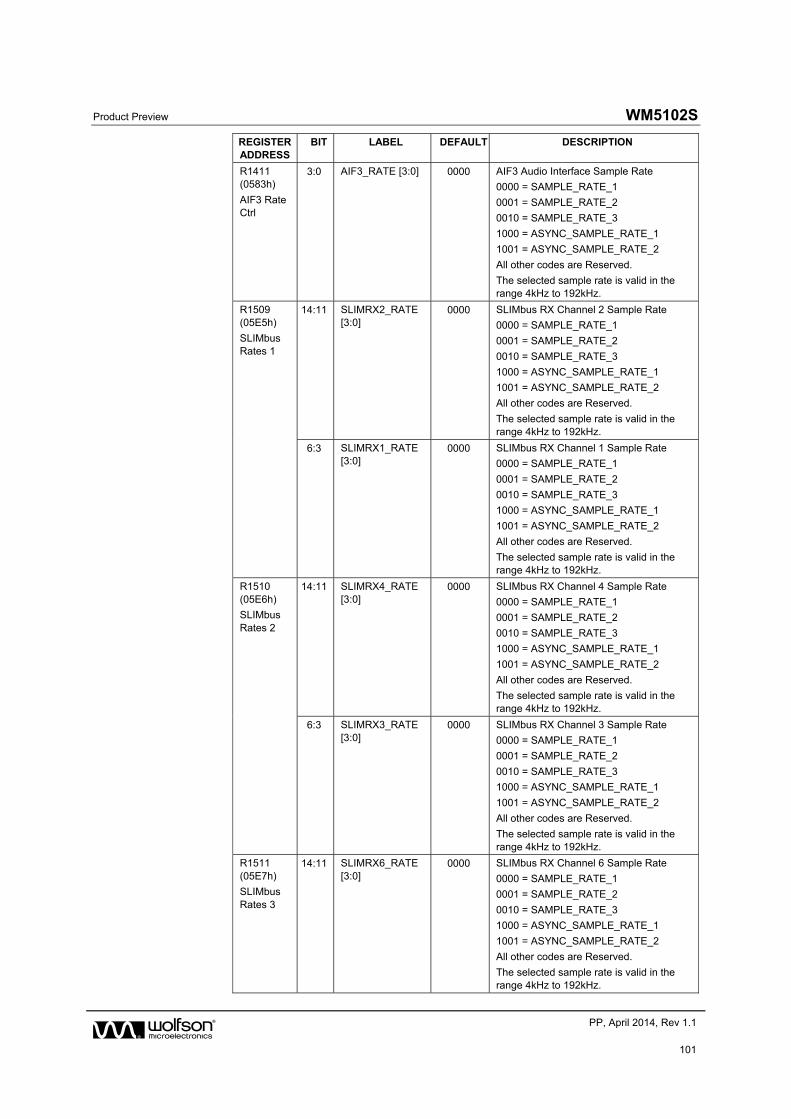
Product Preview WM5102S
w PP, April 2014, Rev 1.1
101
REGISTER ADDRESS
BIT LABEL DEFAULT DESCRIPTION
R1411 (0583h)
AIF3 Rate Ctrl
3:0 AIF3_RATE [3:0] 0000 AIF3 Audio Interface Sample Rate
0000 = SAMPLE_RATE_1
0001 = SAMPLE_RATE_2
0010 = SAMPLE_RATE_3
1000 = ASYNC_SAMPLE_RATE_1
1001 = ASYNC_SAMPLE_RATE_2
All other codes are Reserved.
The selected sample rate is valid in the range 4kHz to 192kHz.
R1509 (05E5h)
SLIMbus Rates 1
14:11 SLIMRX2_RATE [3:0]
0000 SLIMbus RX Channel 2 Sample Rate
0000 = SAMPLE_RATE_1
0001 = SAMPLE_RATE_2
0010 = SAMPLE_RATE_3
1000 = ASYNC_SAMPLE_RATE_1
1001 = ASYNC_SAMPLE_RATE_2
All other codes are Reserved.
The selected sample rate is valid in the range 4kHz to 192kHz.
6:3 SLIMRX1_RATE [3:0]
0000 SLIMbus RX Channel 1 Sample Rate
0000 = SAMPLE_RATE_1
0001 = SAMPLE_RATE_2
0010 = SAMPLE_RATE_3
1000 = ASYNC_SAMPLE_RATE_1
1001 = ASYNC_SAMPLE_RATE_2
All other codes are Reserved.
The selected sample rate is valid in the range 4kHz to 192kHz.
R1510 (05E6h)
SLIMbus Rates 2
14:11 SLIMRX4_RATE [3:0]
0000 SLIMbus RX Channel 4 Sample Rate
0000 = SAMPLE_RATE_1
0001 = SAMPLE_RATE_2
0010 = SAMPLE_RATE_3
1000 = ASYNC_SAMPLE_RATE_1
1001 = ASYNC_SAMPLE_RATE_2
All other codes are Reserved.
The selected sample rate is valid in the range 4kHz to 192kHz.
6:3 SLIMRX3_RATE [3:0]
0000 SLIMbus RX Channel 3 Sample Rate
0000 = SAMPLE_RATE_1
0001 = SAMPLE_RATE_2
0010 = SAMPLE_RATE_3
1000 = ASYNC_SAMPLE_RATE_1
1001 = ASYNC_SAMPLE_RATE_2
All other codes are Reserved.
The selected sample rate is valid in the range 4kHz to 192kHz.
R1511 (05E7h)
SLIMbus Rates 3
14:11 SLIMRX6_RATE [3:0]
0000 SLIMbus RX Channel 6 Sample Rate
0000 = SAMPLE_RATE_1
0001 = SAMPLE_RATE_2
0010 = SAMPLE_RATE_3
1000 = ASYNC_SAMPLE_RATE_1
1001 = ASYNC_SAMPLE_RATE_2
All other codes are Reserved.
The selected sample rate is valid in the range 4kHz to 192kHz.
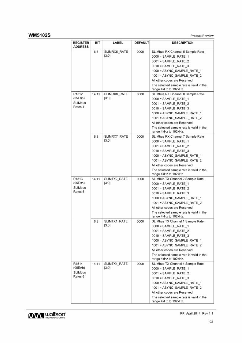
WM5102S Product Preview
w PP, April 2014, Rev 1.1
102
REGISTER ADDRESS
BIT LABEL DEFAULT DESCRIPTION
6:3 SLIMRX5_RATE [3:0]
0000 SLIMbus RX Channel 5 Sample Rate
0000 = SAMPLE_RATE_1
0001 = SAMPLE_RATE_2
0010 = SAMPLE_RATE_3
1000 = ASYNC_SAMPLE_RATE_1
1001 = ASYNC_SAMPLE_RATE_2
All other codes are Reserved.
The selected sample rate is valid in the range 4kHz to 192kHz.
R1512 (05E8h)
SLIMbus Rates 4
14:11 SLIMRX8_RATE [3:0]
0000 SLIMbus RX Channel 8 Sample Rate
0000 = SAMPLE_RATE_1
0001 = SAMPLE_RATE_2
0010 = SAMPLE_RATE_3
1000 = ASYNC_SAMPLE_RATE_1
1001 = ASYNC_SAMPLE_RATE_2
All other codes are Reserved.
The selected sample rate is valid in the range 4kHz to 192kHz.
6:3 SLIMRX7_RATE [3:0]
0000 SLIMbus RX Channel 7 Sample Rate
0000 = SAMPLE_RATE_1
0001 = SAMPLE_RATE_2
0010 = SAMPLE_RATE_3
1000 = ASYNC_SAMPLE_RATE_1
1001 = ASYNC_SAMPLE_RATE_2
All other codes are Reserved.
The selected sample rate is valid in the range 4kHz to 192kHz.
R1513 (05E9h)
SLIMbus Rates 5
14:11 SLIMTX2_RATE [3:0]
0000 SLIMbus TX Channel 2 Sample Rate
0000 = SAMPLE_RATE_1
0001 = SAMPLE_RATE_2
0010 = SAMPLE_RATE_3
1000 = ASYNC_SAMPLE_RATE_1
1001 = ASYNC_SAMPLE_RATE_2
All other codes are Reserved.
The selected sample rate is valid in the range 4kHz to 192kHz.
6:3 SLIMTX1_RATE [3:0]
0000 SLIMbus TX Channel 1 Sample Rate
0000 = SAMPLE_RATE_1
0001 = SAMPLE_RATE_2
0010 = SAMPLE_RATE_3
1000 = ASYNC_SAMPLE_RATE_1
1001 = ASYNC_SAMPLE_RATE_2
All other codes are Reserved.
The selected sample rate is valid in the range 4kHz to 192kHz.
R1514 (05EAh)
SLIMbus Rates 6
14:11 SLIMTX4_RATE [3:0]
0000 SLIMbus TX Channel 4 Sample Rate
0000 = SAMPLE_RATE_1
0001 = SAMPLE_RATE_2
0010 = SAMPLE_RATE_3
1000 = ASYNC_SAMPLE_RATE_1
1001 = ASYNC_SAMPLE_RATE_2
All other codes are Reserved.
The selected sample rate is valid in the range 4kHz to 192kHz.
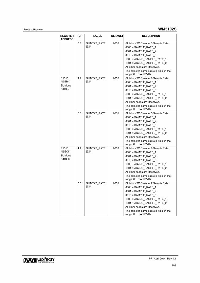
Product Preview WM5102S
w PP, April 2014, Rev 1.1
103
REGISTER ADDRESS
BIT LABEL DEFAULT DESCRIPTION
6:3 SLIMTX3_RATE [3:0]
0000 SLIMbus TX Channel 3 Sample Rate
0000 = SAMPLE_RATE_1
0001 = SAMPLE_RATE_2
0010 = SAMPLE_RATE_3
1000 = ASYNC_SAMPLE_RATE_1
1001 = ASYNC_SAMPLE_RATE_2
All other codes are Reserved.
The selected sample rate is valid in the range 4kHz to 192kHz.
R1515 (05EBh)
SLIMbus Rates 7
14:11 SLIMTX6_RATE [3:0]
0000 SLIMbus TX Channel 6 Sample Rate
0000 = SAMPLE_RATE_1
0001 = SAMPLE_RATE_2
0010 = SAMPLE_RATE_3
1000 = ASYNC_SAMPLE_RATE_1
1001 = ASYNC_SAMPLE_RATE_2
All other codes are Reserved.
The selected sample rate is valid in the range 4kHz to 192kHz.
6:3 SLIMTX5_RATE [3:0]
0000 SLIMbus TX Channel 5 Sample Rate
0000 = SAMPLE_RATE_1
0001 = SAMPLE_RATE_2
0010 = SAMPLE_RATE_3
1000 = ASYNC_SAMPLE_RATE_1
1001 = ASYNC_SAMPLE_RATE_2
All other codes are Reserved.
The selected sample rate is valid in the range 4kHz to 192kHz.
R1516 (05ECh)
SLIMbus Rates 8
14:11 SLIMTX8_RATE [3:0]
0000 SLIMbus TX Channel 8 Sample Rate
0000 = SAMPLE_RATE_1
0001 = SAMPLE_RATE_2
0010 = SAMPLE_RATE_3
1000 = ASYNC_SAMPLE_RATE_1
1001 = ASYNC_SAMPLE_RATE_2
All other codes are Reserved.
The selected sample rate is valid in the range 4kHz to 192kHz.
6:3 SLIMTX7_RATE [3:0]
0000 SLIMbus TX Channel 7 Sample Rate
0000 = SAMPLE_RATE_1
0001 = SAMPLE_RATE_2
0010 = SAMPLE_RATE_3
1000 = ASYNC_SAMPLE_RATE_1
1001 = ASYNC_SAMPLE_RATE_2
All other codes are Reserved.
The selected sample rate is valid in the range 4kHz to 192kHz.
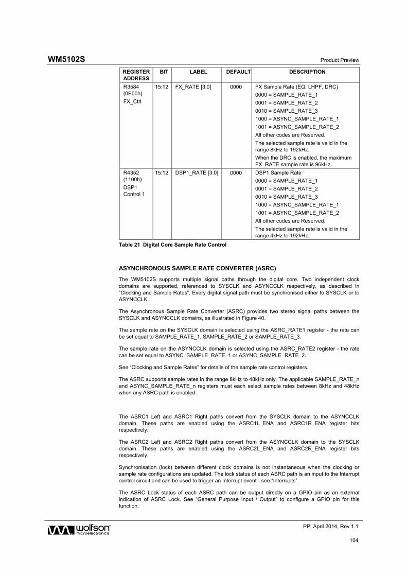
WM5102S Product Preview
w PP, April 2014, Rev 1.1
104
REGISTER ADDRESS
BIT LABEL DEFAULT DESCRIPTION
R3584 (0E00h)
FX_Ctrl
15:12 FX_RATE [3:0] 0000 FX Sample Rate (EQ, LHPF, DRC)
0000 = SAMPLE_RATE_1
0001 = SAMPLE_RATE_2
0010 = SAMPLE_RATE_3
1000 = ASYNC_SAMPLE_RATE_1
1001 = ASYNC_SAMPLE_RATE_2
All other codes are Reserved.
The selected sample rate is valid in the range 8kHz to 192kHz.
When the DRC is enabled, the maximum FX_RATE sample rate is 96kHz.
R4352 (1100h)
DSP1 Control 1
15:12 DSP1_RATE [3:0] 0000 DSP1 Sample Rate
0000 = SAMPLE_RATE_1
0001 = SAMPLE_RATE_2
0010 = SAMPLE_RATE_3
1000 = ASYNC_SAMPLE_RATE_1
1001 = ASYNC_SAMPLE_RATE_2
All other codes are Reserved.
The selected sample rate is valid in the range 4kHz to 192kHz.
Table 21 Digital Core Sample Rate Control
ASYNCHRONOUS SAMPLE RATE CONVERTER (ASRC)
The WM5102S supports multiple signal paths through the digital core. Two independent clock domains are supported, referenced to SYSCLK and ASYNCCLK respectively, as described in “Clocking and Sample Rates”. Every digital signal path must be synchronised either to SYSCLK or to ASYNCCLK.
The Asynchronous Sample Rate Converter (ASRC) provides two stereo signal paths between the SYSCLK and ASYNCCLK domains, as illustrated in Figure 40.
The sample rate on the SYSCLK domain is selected using the ASRC_RATE1 register - the rate can be set equal to SAMPLE_RATE_1, SAMPLE_RATE_2 or SAMPLE_RATE_3.
The sample rate on the ASYNCCLK domain is selected using the ASRC_RATE2 register - the rate can be set equal to ASYNC_SAMPLE_RATE_1 or ASYNC_SAMPLE_RATE_2.
See “Clocking and Sample Rates” for details of the sample rate control registers.
The ASRC supports sample rates in the range 8kHz to 48kHz only. The applicable SAMPLE_RATE_n and ASYNC_SAMPLE_RATE_n registers must each select sample rates between 8kHz and 48kHz when any ASRC path is enabled.
The ASRC1 Left and ASRC1 Right paths convert from the SYSCLK domain to the ASYNCCLK domain. These paths are enabled using the ASRC1L_ENA and ASRC1R_ENA register bits respectively.
The ASRC2 Left and ASRC2 Right paths convert from the ASYNCCLK domain to the SYSCLK domain. These paths are enabled using the ASRC2L_ENA and ASRC2R_ENA register bits respectively.
Synchronisation (lock) between different clock domains is not instantaneous when the clocking or sample rate configurations are updated. The lock status of each ASRC path is an input to the Interrupt control circuit and can be used to trigger an Interrupt event - see “Interrupts”.
The ASRC Lock status of each ASRC path can be output directly on a GPIO pin as an external indication of ASRC Lock. See “General Purpose Input / Output” to configure a GPIO pin for this function.
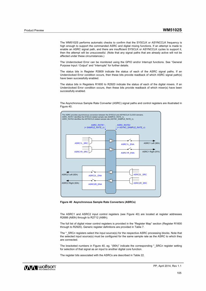
Product Preview WM5102S
w PP, April 2014, Rev 1.1
105
The WM5102S performs automatic checks to confirm that the SYSCLK or ASYNCCLK frequency is high enough to support the commanded ASRC and digital mixing functions. If an attempt is made to enable an ASRC signal path, and there are insufficient SYSCLK or ASYNCCLK cycles to support it, then the attempt will be unsuccessful. (Note that any signal paths that are already active will not be affected under these circumstances.)
The Underclocked Error can be monitored using the GPIO and/or Interrupt functions. See “General Purpose Input / Output” and “Interrupts” for further details.
The status bits in Register R3809 indicate the status of each of the ASRC signal paths. If an Underclocked Error condition occurs, then these bits provide readback of which ASRC signal path(s) have been successfully enabled.
The status bits in Registers R1600 to R2920 indicate the status of each of the digital mixers. If an Underclocked Error condition occurs, then these bits provide readback of which mixer(s) have been successfully enabled.
The Asynchronous Sample Rate Converter (ASRC) signal paths and control registers are illustrated in Figure 40.
ASRC1R_ENA
ASRC1L_ENAASRC1L_SRC
ASRC1R_SRC
ASRC1 Left (90h)
ASRC1 Right (91h)
ASRC2R_ENA
ASRC2L_ENA ASRC2L_SRC
ASRC2R_SRC
ASRC2 Left (92h)
ASRC2 Right (93h)
ASRC_RATE1(= SAMPLE_RATE_n)
ASRC_RATE2(= ASYNC_SAMPLE_RATE_n)
The ASRC provides asynchronous conversion between the SYSCLK and ASYNCCLK CLOCK domains.ASRC_RATE1 identifies the SYSCLK-related sample rate (SAMPLE_RATE_n).ASRC_RATE2 identifies the ASYNCCLK-related sample rate (ASYNC_SAMPLE_RATE_n).
Figure 40 Asynchronous Sample Rate Converters (ASRCs)
The ASRC1 and ASRC2 input control registers (see Figure 40) are located at register addresses R2688 (A80h) through to R2712 (A98h).
The full list of digital mixer control registers is provided in the “Register Map” section (Register R1600 through to R2920). Generic register definitions are provided in Table 7.
The *_SRCn registers select the input source(s) for the respective ASRC processing blocks. Note that the selected input source(s) must be configured for the same sample rate as the ASRC to which they are connected.
The bracketed numbers in Figure 40, eg. “(90h)” indicate the corresponding *_SRCn register setting for selection of that signal as an input to another digital core function.
The register bits associated with the ASRCs are described in Table 22.
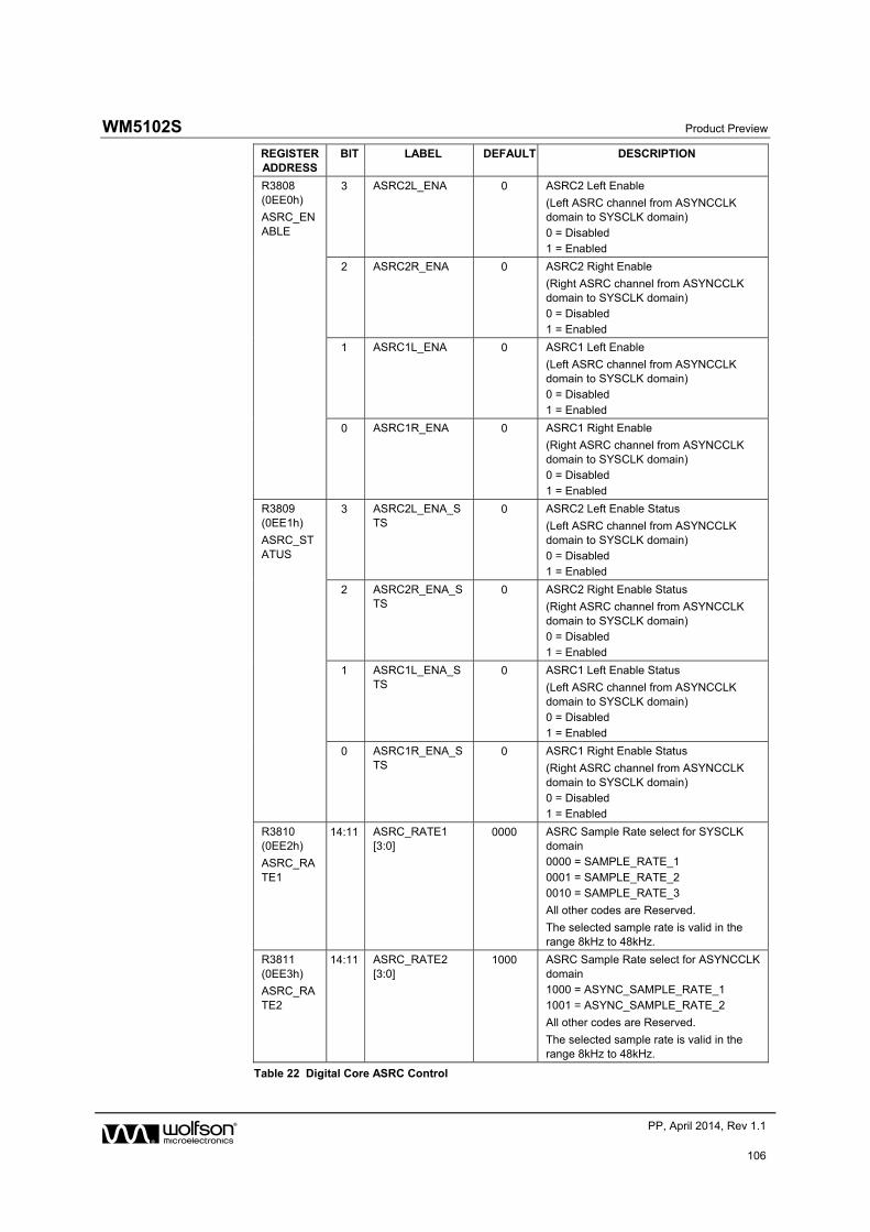
WM5102S Product Preview
w PP, April 2014, Rev 1.1
106
REGISTER ADDRESS
BIT LABEL DEFAULT DESCRIPTION
R3808 (0EE0h)
ASRC_ENABLE
3 ASRC2L_ENA 0 ASRC2 Left Enable
(Left ASRC channel from ASYNCCLK domain to SYSCLK domain) 0 = Disabled 1 = Enabled
2 ASRC2R_ENA 0 ASRC2 Right Enable
(Right ASRC channel from ASYNCCLK domain to SYSCLK domain) 0 = Disabled 1 = Enabled
1 ASRC1L_ENA 0 ASRC1 Left Enable
(Left ASRC channel from ASYNCCLK domain to SYSCLK domain) 0 = Disabled 1 = Enabled
0 ASRC1R_ENA 0 ASRC1 Right Enable
(Right ASRC channel from ASYNCCLK domain to SYSCLK domain) 0 = Disabled 1 = Enabled
R3809 (0EE1h)
ASRC_STATUS
3 ASRC2L_ENA_STS
0 ASRC2 Left Enable Status
(Left ASRC channel from ASYNCCLK domain to SYSCLK domain) 0 = Disabled 1 = Enabled
2 ASRC2R_ENA_STS
0 ASRC2 Right Enable Status
(Right ASRC channel from ASYNCCLK domain to SYSCLK domain) 0 = Disabled 1 = Enabled
1 ASRC1L_ENA_STS
0 ASRC1 Left Enable Status
(Left ASRC channel from ASYNCCLK domain to SYSCLK domain) 0 = Disabled 1 = Enabled
0 ASRC1R_ENA_STS
0 ASRC1 Right Enable Status
(Right ASRC channel from ASYNCCLK domain to SYSCLK domain) 0 = Disabled 1 = Enabled
R3810 (0EE2h)
ASRC_RATE1
14:11 ASRC_RATE1 [3:0]
0000 ASRC Sample Rate select for SYSCLK domain 0000 = SAMPLE_RATE_1 0001 = SAMPLE_RATE_2 0010 = SAMPLE_RATE_3
All other codes are Reserved.
The selected sample rate is valid in the range 8kHz to 48kHz.
R3811 (0EE3h)
ASRC_RATE2
14:11 ASRC_RATE2 [3:0]
1000 ASRC Sample Rate select for ASYNCCLK domain 1000 = ASYNC_SAMPLE_RATE_1 1001 = ASYNC_SAMPLE_RATE_2
All other codes are Reserved.
The selected sample rate is valid in the range 8kHz to 48kHz.
Table 22 Digital Core ASRC Control
Product Preview WM5102S
w PP, April 2014, Rev 1.1
107
ISOCHRONOUS SAMPLE RATE CONVERTER (ISRC)
The WM5102S supports multiple signal paths through the digital core. The Isochronous Sample Rate Converters (ISRCs) provide sample rate conversion between synchronised sample rates on the SYSCLK clock domain, or between synchronised sample rates on the ASYNCCLK clock domain.
There are two Isochronous Sample Rate Converters (ISRCs). Each of these provides two signal paths between two different sample rates, as illustrated in Figure 41.
The sample rates associated with each ISRC can be set independently. Note that the two sample rates associated with any single ISRC must both be referenced to the same clock domain (SYSCLK or ASYNCCLK).
When an ISRC is used on the SYSCLK domain, then the associated sample rates may be selected from SAMPLE_RATE_1, SAMPLE_RATE_2 or SAMPLE_RATE_3.
When an ISRC is used on the ASYNCCLK domain, then the associated sample rates are ASYNC_SAMPLE_RATE_1 and ASYNC_SAMPLE_RATE_2.
See “Clocking and Sample Rates” for details of the sample rate control registers.
Each ISRC supports sample rates in the range 8kHz to 192kHz. The higher of the sample rates associated with each ISRC must be an integer multiple of the lower sample rate; integer ratios in the range 1 to 6 are supported.
Each ISRC converts between a sample rate selected by ISRCn_FSL and a sample rate selected by ISRCn_FSH, (where ‘n’ identifies the applicable ISRC 1 or 2). Note that, in each case, the higher of the two sample rates must be selected by ISRCn_FSH.
The ISRCn ‘interpolation’ paths (increasing sample rate) are enabled using the ISRCn_INT1_ENA and ISRCn_INT2_ENA register bits.
The ISRCn ‘decimation’ paths (decreasing sample rate) are enabled using the ISRCn_DEC1_ENA and ISRCn_DEC2_ENA register bits.
A notch filter is provided in each of the ISRC paths; these are enabled using the ISRCn_NOTCH_ENA bits. The filter is configured automatically according to the applicable sample rate(s). It is recommended to enable the filter for typical applications. Disabling the filter will provide maximum ‘pass’ bandwidth, at the expense of degraded stopband attenuation.
The WM5102S performs automatic checks to confirm that the SYSCLK frequency is high enough to support the commanded ISRC and digital mixing functions. If an attempt is made to enable an ISRC signal path, and there are insufficient SYSCLK cycles to support it, then the attempt will be unsuccessful. (Note that any signal paths that are already active will not be affected under these circumstances.)
The Underclocked Error condition can be monitored using the GPIO and/or Interrupt functions. See “General Purpose Input / Output” and “Interrupts” for further details.
The status bits in Registers R1600 to R2920 indicate the status of each of the digital mixers. If an Underclocked Error condition occurs, then these bits provide readback of which mixer(s) have been successfully enabled.
The Isochronous Sample Rate Converter (ISRC) signal paths and control registers are illustrated in Figure 41.
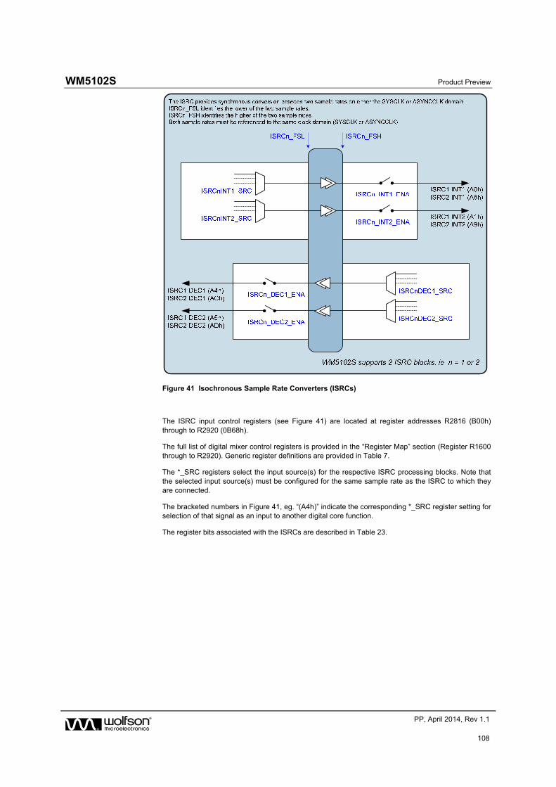
WM5102S Product Preview
w PP, April 2014, Rev 1.1
108
Figure 41 Isochronous Sample Rate Converters (ISRCs)
The ISRC input control registers (see Figure 41) are located at register addresses R2816 (B00h) through to R2920 (0B68h).
The full list of digital mixer control registers is provided in the “Register Map” section (Register R1600 through to R2920). Generic register definitions are provided in Table 7.
The *_SRC registers select the input source(s) for the respective ISRC processing blocks. Note that the selected input source(s) must be configured for the same sample rate as the ISRC to which they are connected.
The bracketed numbers in Figure 41, eg. “(A4h)” indicate the corresponding *_SRC register setting for selection of that signal as an input to another digital core function.
The register bits associated with the ISRCs are described in Table 23.
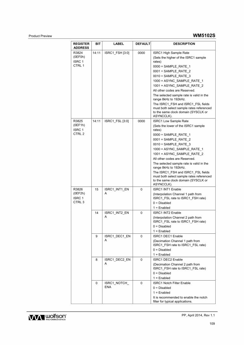
Product Preview WM5102S
w PP, April 2014, Rev 1.1
109
REGISTER ADDRESS
BIT LABEL DEFAULT DESCRIPTION
R3824 (0EF0h)
ISRC 1 CTRL 1
14:11 ISRC1_FSH [3:0] 0000 ISRC1 High Sample Rate
(Sets the higher of the ISRC1 sample rates)
0000 = SAMPLE_RATE_1
0001 = SAMPLE_RATE_2
0010 = SAMPLE_RATE_3
1000 = ASYNC_SAMPLE_RATE_1
1001 = ASYNC_SAMPLE_RATE_2
All other codes are Reserved.
The selected sample rate is valid in the range 8kHz to 192kHz.
The ISRC1_FSH and ISRC1_FSL fields must both select sample rates referenced to the same clock domain (SYSCLK or ASYNCCLK).
R3825 (0EF1h)
ISRC 1 CTRL 2
14:11 ISRC1_FSL [3:0] 0000 ISRC1 Low Sample Rate
(Sets the lower of the ISRC1 sample rates)
0000 = SAMPLE_RATE_1
0001 = SAMPLE_RATE_2
0010 = SAMPLE_RATE_3
1000 = ASYNC_SAMPLE_RATE_1
1001 = ASYNC_SAMPLE_RATE_2
All other codes are Reserved.
The selected sample rate is valid in the range 8kHz to 192kHz.
The ISRC1_FSH and ISRC1_FSL fields must both select sample rates referenced to the same clock domain (SYSCLK or ASYNCCLK).
R3826 (0EF2h)
ISRC 1 CTRL 3
15 ISRC1_INT1_ENA
0 ISRC1 INT1 Enable
(Interpolation Channel 1 path from ISRC1_FSL rate to ISRC1_FSH rate)
0 = Disabled
1 = Enabled
14 ISRC1_INT2_ENA
0 ISRC1 INT2 Enable
(Interpolation Channel 2 path from ISRC1_FSL rate to ISRC1_FSH rate)
0 = Disabled
1 = Enabled
9 ISRC1_DEC1_ENA
0 ISRC1 DEC1 Enable
(Decimation Channel 1 path from ISRC1_FSH rate to ISRC1_FSL rate)
0 = Disabled
1 = Enabled
8 ISRC1_DEC2_ENA
0 ISRC1 DEC2 Enable
(Decimation Channel 2 path from ISRC1_FSH rate to ISRC1_FSL rate)
0 = Disabled
1 = Enabled
0 ISRC1_NOTCH_ENA
0 ISRC1 Notch Filter Enable
0 = Disabled
1 = Enabled
It is recommended to enable the notch filter for typical applications.
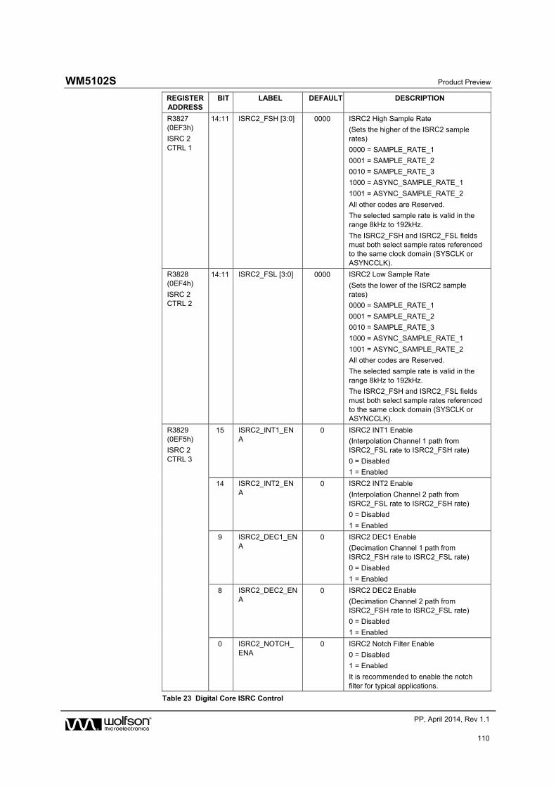
WM5102S Product Preview
w PP, April 2014, Rev 1.1
110
REGISTER ADDRESS
BIT LABEL DEFAULT DESCRIPTION
R3827 (0EF3h)
ISRC 2 CTRL 1
14:11 ISRC2_FSH [3:0] 0000 ISRC2 High Sample Rate
(Sets the higher of the ISRC2 sample rates)
0000 = SAMPLE_RATE_1
0001 = SAMPLE_RATE_2
0010 = SAMPLE_RATE_3
1000 = ASYNC_SAMPLE_RATE_1
1001 = ASYNC_SAMPLE_RATE_2
All other codes are Reserved.
The selected sample rate is valid in the range 8kHz to 192kHz.
The ISRC2_FSH and ISRC2_FSL fields must both select sample rates referenced to the same clock domain (SYSCLK or ASYNCCLK).
R3828 (0EF4h)
ISRC 2 CTRL 2
14:11 ISRC2_FSL [3:0] 0000 ISRC2 Low Sample Rate
(Sets the lower of the ISRC2 sample rates)
0000 = SAMPLE_RATE_1
0001 = SAMPLE_RATE_2
0010 = SAMPLE_RATE_3
1000 = ASYNC_SAMPLE_RATE_1
1001 = ASYNC_SAMPLE_RATE_2
All other codes are Reserved.
The selected sample rate is valid in the range 8kHz to 192kHz.
The ISRC2_FSH and ISRC2_FSL fields must both select sample rates referenced to the same clock domain (SYSCLK or ASYNCCLK).
R3829 (0EF5h)
ISRC 2 CTRL 3
15 ISRC2_INT1_ENA
0 ISRC2 INT1 Enable
(Interpolation Channel 1 path from ISRC2_FSL rate to ISRC2_FSH rate)
0 = Disabled
1 = Enabled
14 ISRC2_INT2_ENA
0 ISRC2 INT2 Enable
(Interpolation Channel 2 path from ISRC2_FSL rate to ISRC2_FSH rate)
0 = Disabled
1 = Enabled
9 ISRC2_DEC1_ENA
0 ISRC2 DEC1 Enable
(Decimation Channel 1 path from ISRC2_FSH rate to ISRC2_FSL rate)
0 = Disabled
1 = Enabled
8 ISRC2_DEC2_ENA
0 ISRC2 DEC2 Enable
(Decimation Channel 2 path from ISRC2_FSH rate to ISRC2_FSL rate)
0 = Disabled
1 = Enabled
0 ISRC2_NOTCH_ENA
0 ISRC2 Notch Filter Enable
0 = Disabled
1 = Enabled
It is recommended to enable the notch filter for typical applications.
Table 23 Digital Core ISRC Control
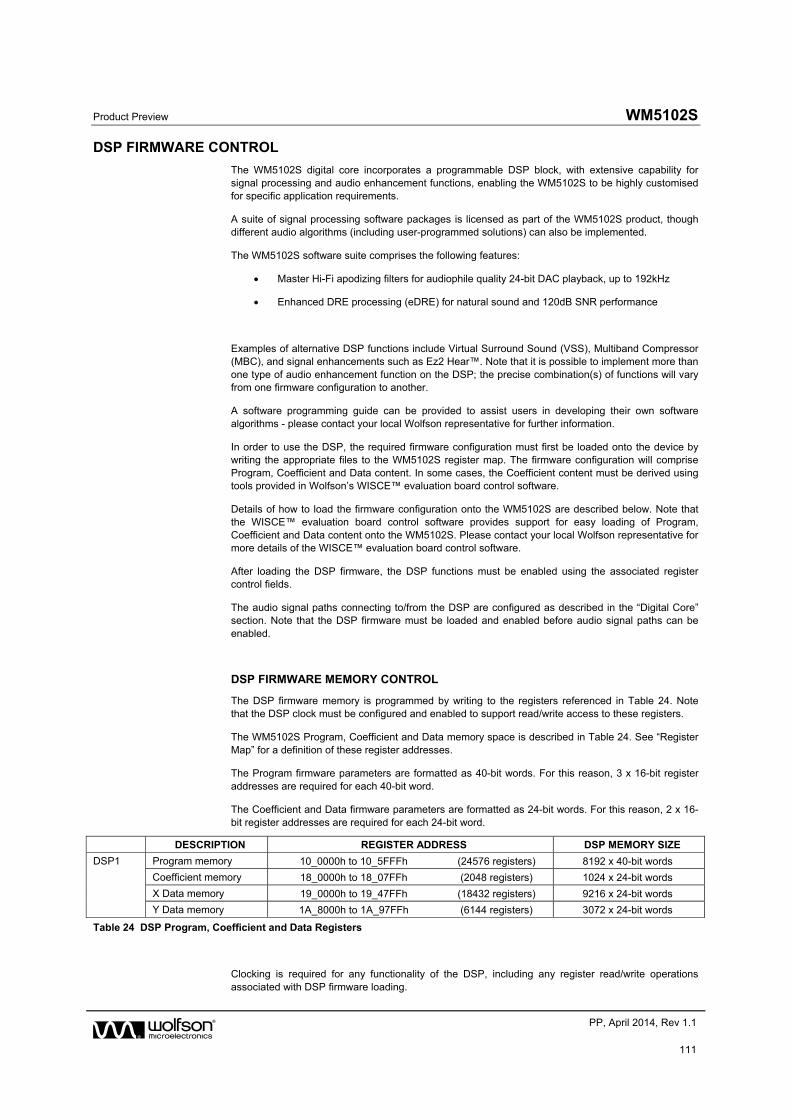
Product Preview WM5102S
w PP, April 2014, Rev 1.1
111
DSP FIRMWARE CONTROL
The WM5102S digital core incorporates a programmable DSP block, with extensive capability for signal processing and audio enhancement functions, enabling the WM5102S to be highly customised for specific application requirements.
A suite of signal processing software packages is licensed as part of the WM5102S product, though different audio algorithms (including user-programmed solutions) can also be implemented.
The WM5102S software suite comprises the following features:
Master Hi-Fi apodizing filters for audiophile quality 24-bit DAC playback, up to 192kHz
Enhanced DRE processing (eDRE) for natural sound and 120dB SNR performance
Examples of alternative DSP functions include Virtual Surround Sound (VSS), Multiband Compressor (MBC), and signal enhancements such as Ez2 Hear™. Note that it is possible to implement more than one type of audio enhancement function on the DSP; the precise combination(s) of functions will vary from one firmware configuration to another.
A software programming guide can be provided to assist users in developing their own software algorithms - please contact your local Wolfson representative for further information.
In order to use the DSP, the required firmware configuration must first be loaded onto the device by writing the appropriate files to the WM5102S register map. The firmware configuration will comprise Program, Coefficient and Data content. In some cases, the Coefficient content must be derived using tools provided in Wolfson’s WISCE™ evaluation board control software.
Details of how to load the firmware configuration onto the WM5102S are described below. Note that the WISCE™ evaluation board control software provides support for easy loading of Program, Coefficient and Data content onto the WM5102S. Please contact your local Wolfson representative for more details of the WISCE™ evaluation board control software.
After loading the DSP firmware, the DSP functions must be enabled using the associated register control fields.
The audio signal paths connecting to/from the DSP are configured as described in the “Digital Core” section. Note that the DSP firmware must be loaded and enabled before audio signal paths can be enabled.
DSP FIRMWARE MEMORY CONTROL
The DSP firmware memory is programmed by writing to the registers referenced in Table 24. Note that the DSP clock must be configured and enabled to support read/write access to these registers.
The WM5102S Program, Coefficient and Data memory space is described in Table 24. See “Register Map” for a definition of these register addresses.
The Program firmware parameters are formatted as 40-bit words. For this reason, 3 x 16-bit register addresses are required for each 40-bit word.
The Coefficient and Data firmware parameters are formatted as 24-bit words. For this reason, 2 x 16-bit register addresses are required for each 24-bit word.
DESCRIPTION REGISTER ADDRESS DSP MEMORY SIZE
DSP1 Program memory 10_0000h to 10_5FFFh (24576 registers) 8192 x 40-bit words
Coefficient memory 18_0000h to 18_07FFh (2048 registers) 1024 x 24-bit words
X Data memory 19_0000h to 19_47FFh (18432 registers) 9216 x 24-bit words
Y Data memory 1A_8000h to 1A_97FFh (6144 registers) 3072 x 24-bit words
Table 24 DSP Program, Coefficient and Data Registers
Clocking is required for any functionality of the DSP, including any register read/write operations associated with DSP firmware loading.
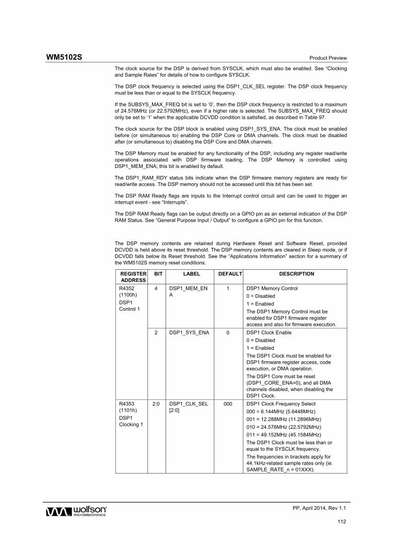
WM5102S Product Preview
w PP, April 2014, Rev 1.1
112
The clock source for the DSP is derived from SYSCLK, which must also be enabled. See “Clocking and Sample Rates” for details of how to configure SYSCLK.
The DSP clock frequency is selected using the DSP1_CLK_SEL register. The DSP clock frequency must be less than or equal to the SYSCLK frequency.
If the SUBSYS_MAX_FREQ bit is set to ‘0’, then the DSP clock frequency is restricted to a maximum of 24.576MHz (or 22.5792MHz), even if a higher rate is selected. The SUBSYS_MAX_FREQ should only be set to ‘1’ when the applicable DCVDD condition is satisfied, as described in Table 97.
The clock source for the DSP block is enabled using DSP1_SYS_ENA. The clock must be enabled before (or simultaneous to) enabling the DSP Core or DMA channels. The clock must be disabled after (or simultaneous to) disabling the DSP Core and DMA channels.
The DSP Memory must be enabled for any functionality of the DSP, including any register read/write operations associated with DSP firmware loading. The DSP Memory is controlled using DSP1_MEM_ENA; this bit is enabled by default.
The DSP1_RAM_RDY status bits indicate when the DSP firmware memory registers are ready for read/write access. The DSP memory should not be accessed until this bit has been set.
The DSP RAM Ready flags are inputs to the Interrupt control circuit and can be used to trigger an interrupt event - see “Interrupts”.
The DSP RAM Ready flags can be output directly on a GPIO pin as an external indication of the DSP RAM Status. See “General Purpose Input / Output” to configure a GPIO pin for this function.
The DSP memory contents are retained during Hardware Reset and Software Reset, provided DCVDD is held above its reset threshold. The DSP memory contents are cleared in Sleep mode, or if DCVDD falls below its Reset threshold. See the “Applications Information” section for a summary of the WM5102S memory reset conditions.
REGISTER ADDRESS
BIT LABEL DEFAULT DESCRIPTION
R4352 (1100h)
DSP1 Control 1
4 DSP1_MEM_ENA
1 DSP1 Memory Control
0 = Disabled
1 = Enabled
The DSP1 Memory Control must be enabled for DSP1 firmware register access and also for firmware execution.
2 DSP1_SYS_ENA 0 DSP1 Clock Enable
0 = Disabled
1 = Enabled
The DSP1 Clock must be enabled for DSP1 firmware register access, code execution, or DMA operation.
The DSP1 Core must be reset (DSP1_CORE_ENA=0), and all DMA channels disabled, when disabling the DSP1 Clock.
R4353 (1101h)
DSP1 Clocking 1
2:0 DSP1_CLK_SEL [2:0]
000 DSP1 Clock Frequency Select
000 = 6.144MHz (5.6448MHz)
001 = 12.288MHz (11.2896MHz)
010 = 24.576MHz (22.5792MHz)
011 = 49.152MHz (45.1584MHz)
The DSP1 Clock must be less than or equal to the SYSCLK frequency.
The frequencies in brackets apply for 44.1kHz-related sample rates only (ie. SAMPLE_RATE_n = 01XXX).

Product Preview WM5102S
w PP, April 2014, Rev 1.1
113
REGISTER ADDRESS
BIT LABEL DEFAULT DESCRIPTION
R4356 (1104h)
DSP1 Status 1
0 DSP1_RAM_RDY 0 DSP1 Memory Status
0 = Not ready
1 = Ready
Note - DSP1 memory should not be accessed until this bit has been set.
Table 25 DSP Clocking Control
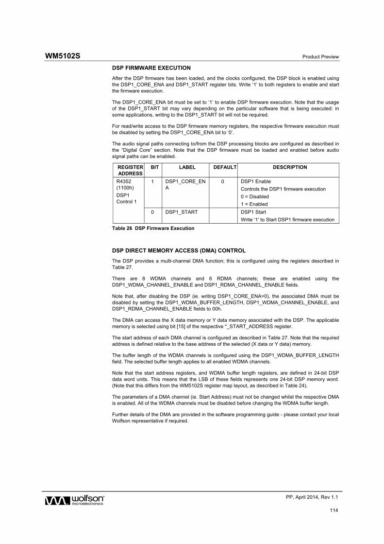
WM5102S Product Preview
w PP, April 2014, Rev 1.1
114
DSP FIRMWARE EXECUTION
After the DSP firmware has been loaded, and the clocks configured, the DSP block is enabled using the DSP1_CORE_ENA and DSP1_START register bits. Write ‘1’ to both registers to enable and start the firmware execution.
The DSP1_CORE_ENA bit must be set to ‘1’ to enable DSP firmware execution. Note that the usage of the DSP1_START bit may vary depending on the particular software that is being executed: in some applications, writing to the DSP1_START bit will not be required.
For read/write access to the DSP firmware memory registers, the respective firmware execution must be disabled by setting the DSP1_CORE_ENA bit to ‘0’.
The audio signal paths connecting to/from the DSP processing blocks are configured as described in the “Digital Core” section. Note that the DSP firmware must be loaded and enabled before audio signal paths can be enabled.
REGISTER ADDRESS
BIT LABEL DEFAULT DESCRIPTION
R4352 (1100h)
DSP1 Control 1
1 DSP1_CORE_ENA
0 DSP1 Enable
Controls the DSP1 firmware execution
0 = Disabled
1 = Enabled
0 DSP1_START DSP1 Start
Write ‘1’ to Start DSP1 firmware execution
Table 26 DSP Firmware Execution
DSP DIRECT MEMORY ACCESS (DMA) CONTROL
The DSP provides a multi-channel DMA function; this is configured using the registers described in Table 27.
There are 8 WDMA channels and 6 RDMA channels; these are enabled using the DSP1_WDMA_CHANNEL_ENABLE and DSP1_RDMA_CHANNEL_ENABLE fields.
Note that, after disabling the DSP (ie. writing DSP1_CORE_ENA=0), the associated DMA must be disabled by setting the DSP1_WDMA_BUFFER_LENGTH, DSP1_WDMA_CHANNEL_ENABLE, and DSP1_RDMA_CHANNEL_ENABLE fields to 00h.
The DMA can access the X data memory or Y data memory associated with the DSP. The applicable memory is selected using bit [15] of the respective *_START_ADDRESS register.
The start address of each DMA channel is configured as described in Table 27. Note that the required address is defined relative to the base address of the selected (X data or Y data) memory.
The buffer length of the WDMA channels is configured using the DSP1_WDMA_BUFFER_LENGTH field. The selected buffer length applies to all enabled WDMA channels.
Note that the start address registers, and WDMA buffer length registers, are defined in 24-bit DSP data word units. This means that the LSB of these fields represents one 24-bit DSP memory word. (Note that this differs from the WM5102S register map layout, as described in Table 24).
The parameters of a DMA channel (ie. Start Address) must not be changed whilst the respective DMA is enabled. All of the WDMA channels must be disabled before changing the WDMA buffer length.
Further details of the DMA are provided in the software programming guide - please contact your local Wolfson representative if required.
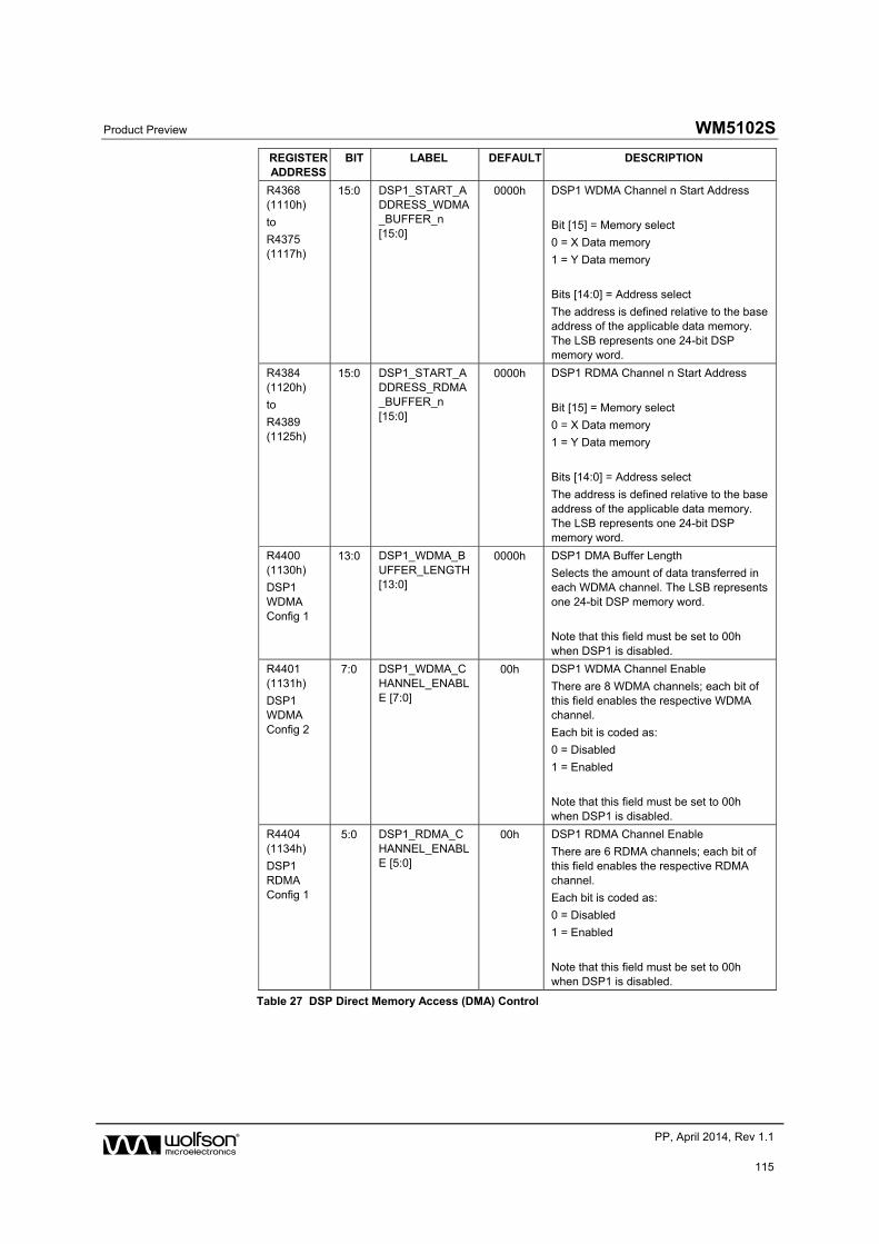
Product Preview WM5102S
w PP, April 2014, Rev 1.1
115
REGISTER ADDRESS
BIT LABEL DEFAULT DESCRIPTION
R4368 (1110h)
to
R4375 (1117h)
15:0 DSP1_START_ADDRESS_WDMA_BUFFER_n [15:0]
0000h DSP1 WDMA Channel n Start Address
Bit [15] = Memory select
0 = X Data memory
1 = Y Data memory
Bits [14:0] = Address select
The address is defined relative to the base address of the applicable data memory. The LSB represents one 24-bit DSP memory word.
R4384 (1120h)
to
R4389 (1125h)
15:0 DSP1_START_ADDRESS_RDMA_BUFFER_n [15:0]
0000h DSP1 RDMA Channel n Start Address
Bit [15] = Memory select
0 = X Data memory
1 = Y Data memory
Bits [14:0] = Address select
The address is defined relative to the base address of the applicable data memory. The LSB represents one 24-bit DSP memory word.
R4400 (1130h)
DSP1 WDMA Config 1
13:0 DSP1_WDMA_BUFFER_LENGTH [13:0]
0000h DSP1 DMA Buffer Length
Selects the amount of data transferred in each WDMA channel. The LSB represents one 24-bit DSP memory word.
Note that this field must be set to 00h when DSP1 is disabled.
R4401 (1131h)
DSP1 WDMA Config 2
7:0 DSP1_WDMA_CHANNEL_ENABLE [7:0]
00h DSP1 WDMA Channel Enable
There are 8 WDMA channels; each bit of this field enables the respective WDMA channel.
Each bit is coded as:
0 = Disabled
1 = Enabled
Note that this field must be set to 00h when DSP1 is disabled.
R4404 (1134h)
DSP1 RDMA Config 1
5:0 DSP1_RDMA_CHANNEL_ENABLE [5:0]
00h DSP1 RDMA Channel Enable
There are 6 RDMA channels; each bit of this field enables the respective RDMA channel.
Each bit is coded as:
0 = Disabled
1 = Enabled
Note that this field must be set to 00h when DSP1 is disabled.
Table 27 DSP Direct Memory Access (DMA) Control
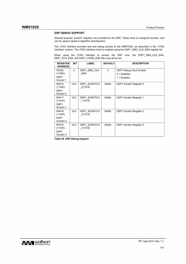
WM5102S Product Preview
w PP, April 2014, Rev 1.1
116
DSP DEBUG SUPPORT
General purpose ‘scratch’ registers are provided for the DSP. These have no assigned function, and can be used to assist in algorithm development.
The JTAG interface provides test and debug access to the WM5102S, as described in the “JTAG Interface” section. The JTAG interface clock is enabled using the DSP1_DBG_CLK_ENA register bit.
When using the JTAG interface to access the DSP core, the DSP1_DBG_CLK_ENA, DSP1_SYS_ENA, and DSP1_CORE_ENA bits must all be set.
REGISTER ADDRESS
BIT LABEL DEFAULT DESCRIPTION
R4352 (1100h)
DSP1 Control 1
3 DSP1_DBG_CLK_ENA
0 DSP1 Debug Clock Enable
0 = Disabled
1 = Enabled
R4416 (1140h)
DSP1 Scratch 0
15:0 DSP1_SCRATCH_0 [15:0]
0000h DSP1 Scratch Register 0
R4417 (1141h)
DSP1 Scratch 1
15:0 DSP1_SCRATCH_1 [15:0]
0000h DSP1 Scratch Register 1
R4418 (1142h)
DSP1 Scratch 2
15:0 DSP1_SCRATCH_2 [15:0]
0000h DSP1 Scratch Register 2
R4419 (1143h)
DSP1 Scratch 3
15:0 DSP1_SCRATCH_3 [15:0]
0000h DSP1 Scratch Register 3
Table 28 DSP Debug Support
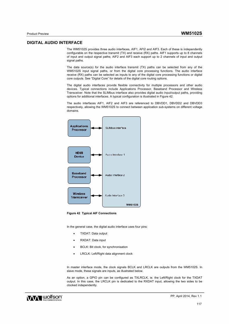
Product Preview WM5102S
w PP, April 2014, Rev 1.1
117
DIGITAL AUDIO INTERFACE
The WM5102S provides three audio interfaces, AIF1, AFI2 and AIF3. Each of these is independently configurable on the respective transmit (TX) and receive (RX) paths. AIF1 supports up to 8 channels of input and output signal paths; AIF2 and AIF3 each support up to 2 channels of input and output signal paths.
The data source(s) for the audio interface transmit (TX) paths can be selected from any of the WM5102S input signal paths, or from the digital core processing functions. The audio interface receive (RX) paths can be selected as inputs to any of the digital core processing functions or digital core outputs. See “Digital Core” for details of the digital core routing options.
The digital audio interfaces provide flexible connectivity for multiple processors and other audio devices. Typical connections include Applications Processor, Baseband Processor and Wireless Transceiver. Note that the SLIMbus interface also provides digital audio input/output paths, providing options for additional interfaces. A typical configuration is illustrated in Figure 42.
The audio interfaces AIF1, AIF2 and AIF3 are referenced to DBVDD1, DBVDD2 and DBVDD3 respectively, allowing the WM5102S to connect between application sub-systems on different voltage domains.
Figure 42 Typical AIF Connections
In the general case, the digital audio interface uses four pins:
TXDAT: Data output
RXDAT: Data input
BCLK: Bit clock, for synchronisation
LRCLK: Left/Right data alignment clock
In master interface mode, the clock signals BCLK and LRCLK are outputs from the WM5102S. In slave mode, these signals are inputs, as illustrated below.
As an option, a GPIO pin can be configured as TXLRCLK, ie. the Left/Right clock for the TXDAT output. In this case, the LRCLK pin is dedicated to the RXDAT input, allowing the two sides to be clocked independently.
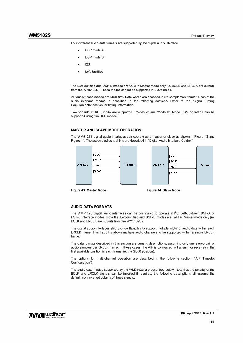
WM5102S Product Preview
w PP, April 2014, Rev 1.1
118
Four different audio data formats are supported by the digital audio interface:
DSP mode A
DSP mode B
I2S
Left Justified
The Left Justified and DSP-B modes are valid in Master mode only (ie. BCLK and LRCLK are outputs from the WM5102S). These modes cannot be supported in Slave mode.
All four of these modes are MSB first. Data words are encoded in 2’s complement format. Each of the audio interface modes is described in the following sections. Refer to the “Signal Timing Requirements” section for timing information.
Two variants of DSP mode are supported - ‘Mode A’ and ‘Mode B’. Mono PCM operation can be supported using the DSP modes.
MASTER AND SLAVE MODE OPERATION
The WM5102S digital audio interfaces can operate as a master or slave as shown in Figure 43 and Figure 44. The associated control bits are described in “Digital Audio Interface Control”.
Figure 43 Master Mode Figure 44 Slave Mode
AUDIO DATA FORMATS
The WM5102S digital audio interfaces can be configured to operate in I2S, Left-Justified, DSP-A or DSP-B interface modes. Note that Left-Justified and DSP-B modes are valid in Master mode only (ie. BCLK and LRCLK are outputs from the WM5102S).
The digital audio interfaces also provide flexibility to support multiple ‘slots’ of audio data within each LRCLK frame. This flexibility allows multiple audio channels to be supported within a single LRCLK frame.
The data formats described in this section are generic descriptions, assuming only one stereo pair of audio samples per LRCLK frame. In these cases, the AIF is configured to transmit (or receive) in the first available position in each frame (ie. the Slot 0 position).
The options for multi-channel operation are described in the following section (“AIF Timeslot Configuration”).
The audio data modes supported by the WM5102S are described below. Note that the polarity of the BCLK and LRCLK signals can be inverted if required; the following descriptions all assume the default, non-inverted polarity of these signals.
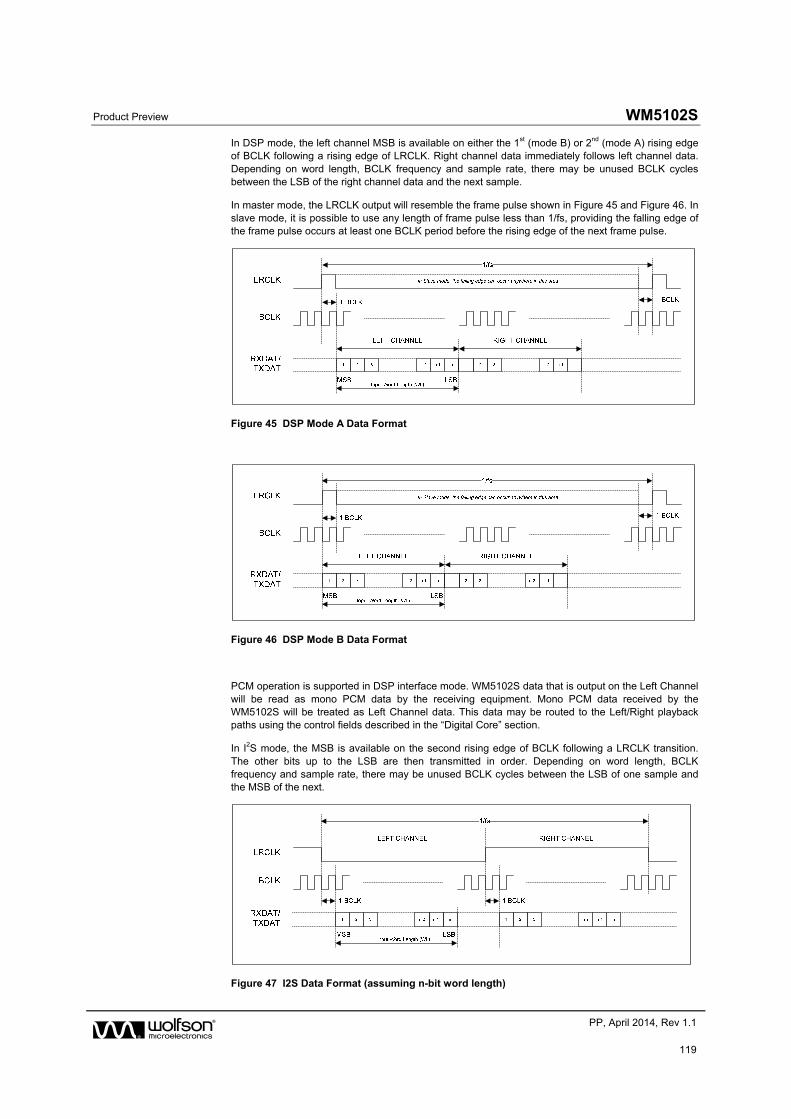
Product Preview WM5102S
w PP, April 2014, Rev 1.1
119
In DSP mode, the left channel MSB is available on either the 1st (mode B) or 2nd (mode A) rising edge of BCLK following a rising edge of LRCLK. Right channel data immediately follows left channel data. Depending on word length, BCLK frequency and sample rate, there may be unused BCLK cycles between the LSB of the right channel data and the next sample.
In master mode, the LRCLK output will resemble the frame pulse shown in Figure 45 and Figure 46. In slave mode, it is possible to use any length of frame pulse less than 1/fs, providing the falling edge of the frame pulse occurs at least one BCLK period before the rising edge of the next frame pulse.
Figure 45 DSP Mode A Data Format
Figure 46 DSP Mode B Data Format
PCM operation is supported in DSP interface mode. WM5102S data that is output on the Left Channel will be read as mono PCM data by the receiving equipment. Mono PCM data received by the WM5102S will be treated as Left Channel data. This data may be routed to the Left/Right playback paths using the control fields described in the “Digital Core” section.
In I2S mode, the MSB is available on the second rising edge of BCLK following a LRCLK transition. The other bits up to the LSB are then transmitted in order. Depending on word length, BCLK frequency and sample rate, there may be unused BCLK cycles between the LSB of one sample and the MSB of the next.
Figure 47 I2S Data Format (assuming n-bit word length)
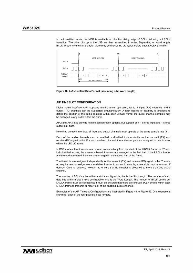
WM5102S Product Preview
w PP, April 2014, Rev 1.1
120
In Left Justified mode, the MSB is available on the first rising edge of BCLK following a LRCLK transition. The other bits up to the LSB are then transmitted in order. Depending on word length, BCLK frequency and sample rate, there may be unused BCLK cycles before each LRCLK transition.
nn-1n-2321 nn-1n-2321
LEFT CHANNEL RIGHT CHANNEL
MSB LSBInput Word Length (WL)
1/fs
LRCLK
BCLK
RXDAT/TXDAT
Figure 48 Left Justified Data Format (assuming n-bit word length)
AIF TIMESLOT CONFIGURATION
Digital audio interface AIF1 supports multi-channel operation; up to 8 input (RX) channels and 8 output (TX) channels can be supported simultaneously. A high degree of flexibility is provided to define the position of the audio samples within each LRCLK frame; the audio channel samples may be arranged in any order within the frame.
AIF2 and AIF3 also provide flexible configuration options, but support only 1 stereo input and 1 stereo output pair each.
Note that, on each interface, all input and output channels must operate at the same sample rate (fs).
Each of the audio channels can be enabled or disabled independently on the transmit (TX) and receive (RX) signal paths. For each enabled channel, the audio samples are assigned to one timeslot within the LRCLK frame.
In DSP modes, the timeslots are ordered consecutively from the start of the LRCLK frame. In I2S and Left-Justified modes, the even-numbered timeslots are arranged in the first half of the LRCLK frame, and the odd-numbered timeslots are arranged in the second half of the frame.
The timeslots are assigned independently for the transmit (TX) and receive (RX) signal paths. There is no requirement to assign every available timeslot to an audio sample; some slots may be unused, if desired. Care is required, however, to ensure that no timeslot is allocated to more than one audio channel.
The number of BCLK cycles within a slot is configurable; this is the Slot Length. The number of valid data bits within a slot is also configurable; this is the Word Length. The number of BCLK cycles per LRCLK frame must be configured; it must be ensured that there are enough BCLK cycles within each LRCLK frame to transmit or receive all of the enabled audio channels.
Examples of the AIF Timeslot Configurations are illustrated in Figure 49 to Figure 52. One example is shown for each of the four possible data formats.
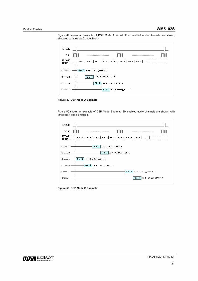
Product Preview WM5102S
w PP, April 2014, Rev 1.1
121
Figure 49 shows an example of DSP Mode A format. Four enabled audio channels are shown, allocated to timeslots 0 through to 3.
Figure 49 DSP Mode A Example
Figure 50 shows an example of DSP Mode B format. Six enabled audio channels are shown, with timeslots 4 and 5 unsused.
Figure 50 DSP Mode B Example
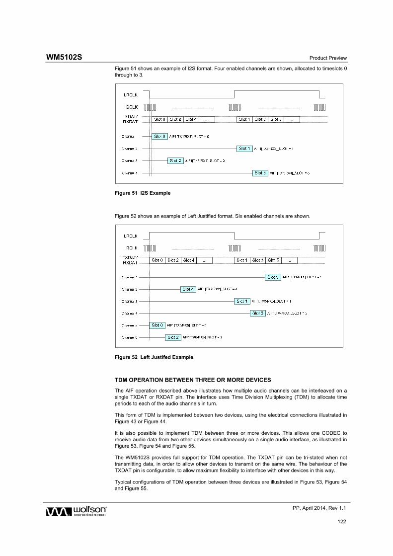
WM5102S Product Preview
w PP, April 2014, Rev 1.1
122
Figure 51 shows an example of I2S format. Four enabled channels are shown, allocated to timeslots 0 through to 3.
Figure 51 I2S Example
Figure 52 shows an example of Left Justified format. Six enabled channels are shown.
Figure 52 Left Justifed Example
TDM OPERATION BETWEEN THREE OR MORE DEVICES
The AIF operation described above illustrates how multiple audio channels can be interleaved on a single TXDAT or RXDAT pin. The interface uses Time Division Multiplexing (TDM) to allocate time periods to each of the audio channels in turn.
This form of TDM is implemented between two devices, using the electrical connections illustrated in Figure 43 or Figure 44.
It is also possible to implement TDM between three or more devices. This allows one CODEC to receive audio data from two other devices simultaneously on a single audio interface, as illustrated in Figure 53, Figure 54 and Figure 55.
The WM5102S provides full support for TDM operation. The TXDAT pin can be tri-stated when not transmitting data, in order to allow other devices to transmit on the same wire. The behaviour of the TXDAT pin is configurable, to allow maximum flexibility to interface with other devices in this way.
Typical configurations of TDM operation between three devices are illustrated in Figure 53, Figure 54 and Figure 55.
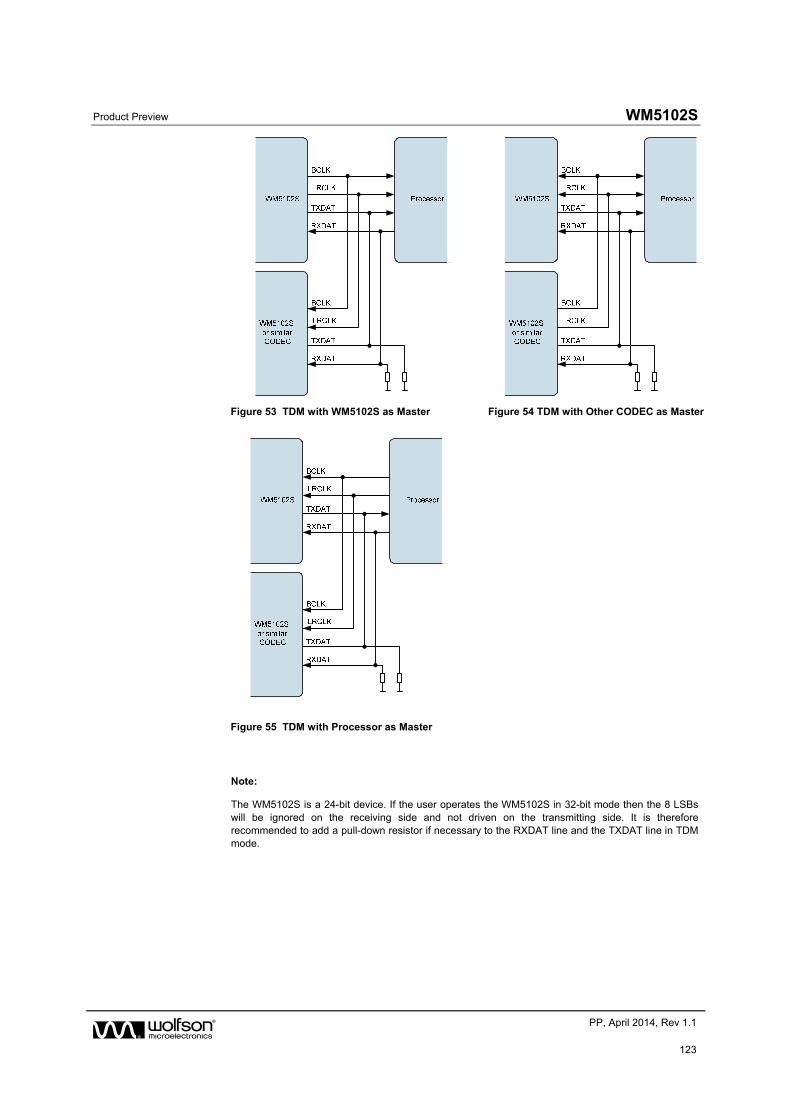
Product Preview WM5102S
w PP, April 2014, Rev 1.1
123
Figure 53 TDM with WM5102S as Master Figure 54 TDM with Other CODEC as Master
Figure 55 TDM with Processor as Master
Note:
The WM5102S is a 24-bit device. If the user operates the WM5102S in 32-bit mode then the 8 LSBs will be ignored on the receiving side and not driven on the transmitting side. It is therefore recommended to add a pull-down resistor if necessary to the RXDAT line and the TXDAT line in TDM mode.
WM5102S Product Preview
w PP, April 2014, Rev 1.1
124
DIGITAL AUDIO INTERFACE CONTROL
This section describes the configuration of the WM5102S digital audio interface paths.
AIF1 supports up to 8 input signal paths and up to 8 output signal paths. AIF2 and AIF3 support up to 2 input and output signal paths each. The digital audio interfaces AIF1, AIF2 and AIF3 can be configured as Master or Slave interfaces; mixed master/slave configurations are also possible.
Each input and output signal path can be independently enabled or disabled. The AIF output (TX) and AIF input (RX) paths can use a common LRCLK frame clock, or can use separate LRCLK signals if required.
The digital audio interface supports flexible data formats, selectable word-length, configurable timeslot allocations and TDM tri-state control.
AIF SAMPLE RATE CONTROL
The AIF RX inputs may be selected as input to the digital mixers or signal processing functions within the WM5102S digital core. The AIF TX outputs are derived from the respective output mixers.
The sample rate for each digital audio interface AIFn is configured using the respective AIFn_RATE register - see Table 21 within the “Digital Core” section.
Note that sample rate conversion is required when routing the AIF paths to any signal chain that is asynchronous and/or configured for a different sample rate.
AIF MASTER / SLAVE CONTROL
The digital audio interfaces can operate in Master or Slave modes and also in mixed master/slave configurations. In Master mode, the BCLK and LRCLK signals are generated by the WM5102S when any of the respective digital audio interface channels is enabled. In Slave mode, these outputs are disabled by default to allow another device to drive these pins.
Master mode is selected on the AIFnBCLK pin using the AIFn_BCLK_MSTR register bit. In Master mode, the AIFnBCLK signal is generated by the WM5102S when one or more AIFn channels is enabled.
When the AIFn_BCLK_FRC bit is set in BCLK master mode, the AIFnBCLK signal is output at all times, including when none of the AIFn channels is enabled.
The AIFnBCLK signal can be inverted in Master or Slave modes using the AIFn_BCLK_INV register.
Master mode is selected on the AIFnLRCLK pin using the AIFnRX_LRCLK_MSTR register bit. In Master mode, the AIFnRXLRCLK signal is generated by the WM5102S when one or more AIFn channels is enabled. (Note that, when GPIOn is configured as AIFnTXLRCLK, then only the AIFn RX channels will cause AIFnRXLRCLK to be output.)
When the AIFnRX_LRCLK_FRC bit is set in LRCLK master mode, the AIFnRXLRCLK signal is output at all times, including when none of the AIFn channels is enabled. Note that AIFnRXLRCLK is derived from AIFnBCLK, and an internal or external AIFnBCLK signal must be present to generate AIFnRXLRCLK.
The AIFnRXLRCLK signal can be inverted in Master or Slave modes using the AIFnRX_LRCLK_INV register.
Under default conditions, the AIFn input (RX) and output (TX) paths both use the AIFnRXLRCLK signal as the frame synchronisation clock. The AIFn output (TX) interface can be configured to use a separate frame clock, AIFnTXLRCLK, using the AIFnTX_LRCLK_SRC bit.
The AIFnTXLRCLK function, when used, must be selected on the GPIOn pin as described in the “General Purpose Input / Output” section.
The AIFnTXLRCLK function can operate in Master or Slave mode, and is controlled similarly to the AIFnRXLRCLK function using the register bits described in Table 29, Table 30 and Table 31 for AIF1, AIF2 and AIF3 respectively.
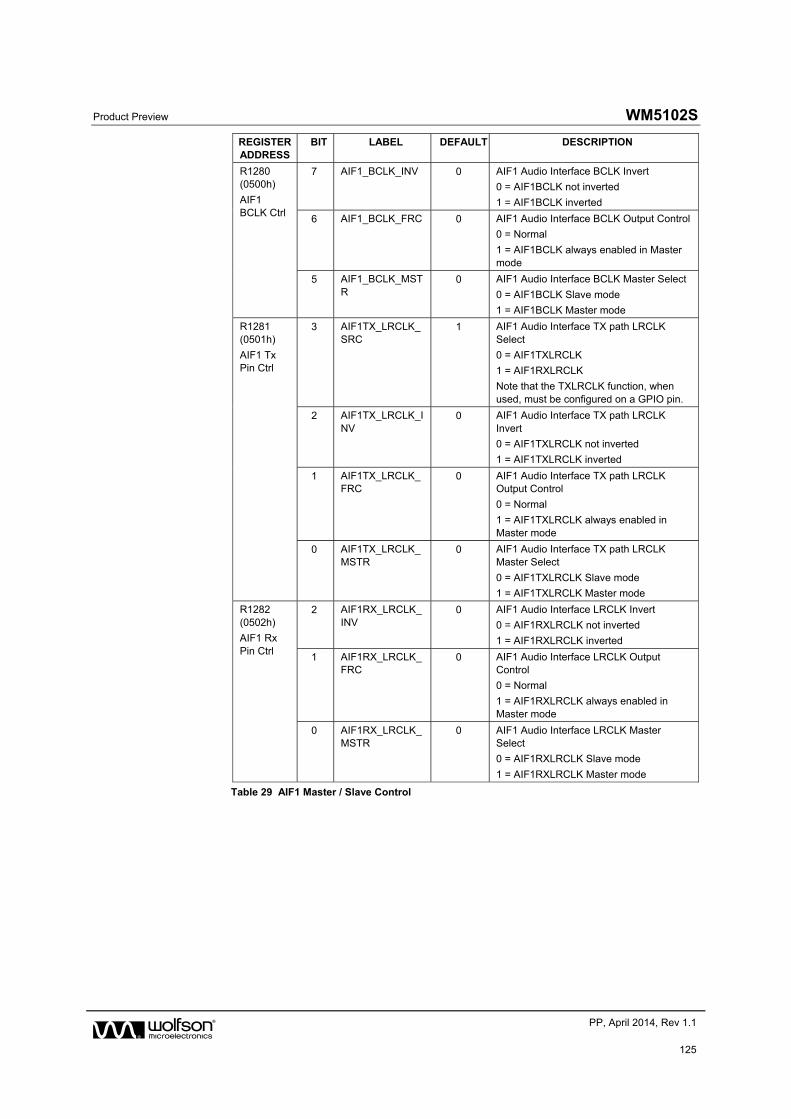
Product Preview WM5102S
w PP, April 2014, Rev 1.1
125
REGISTER ADDRESS
BIT LABEL DEFAULT DESCRIPTION
R1280 (0500h)
AIF1 BCLK Ctrl
7 AIF1_BCLK_INV 0 AIF1 Audio Interface BCLK Invert
0 = AIF1BCLK not inverted
1 = AIF1BCLK inverted
6 AIF1_BCLK_FRC 0 AIF1 Audio Interface BCLK Output Control
0 = Normal
1 = AIF1BCLK always enabled in Master mode
5 AIF1_BCLK_MSTR
0 AIF1 Audio Interface BCLK Master Select
0 = AIF1BCLK Slave mode
1 = AIF1BCLK Master mode
R1281 (0501h)
AIF1 Tx Pin Ctrl
3 AIF1TX_LRCLK_SRC
1 AIF1 Audio Interface TX path LRCLK Select
0 = AIF1TXLRCLK
1 = AIF1RXLRCLK
Note that the TXLRCLK function, when used, must be configured on a GPIO pin.
2 AIF1TX_LRCLK_INV
0 AIF1 Audio Interface TX path LRCLK Invert
0 = AIF1TXLRCLK not inverted
1 = AIF1TXLRCLK inverted
1 AIF1TX_LRCLK_FRC
0 AIF1 Audio Interface TX path LRCLK Output Control
0 = Normal
1 = AIF1TXLRCLK always enabled in Master mode
0 AIF1TX_LRCLK_MSTR
0 AIF1 Audio Interface TX path LRCLK Master Select
0 = AIF1TXLRCLK Slave mode
1 = AIF1TXLRCLK Master mode
R1282 (0502h)
AIF1 Rx Pin Ctrl
2 AIF1RX_LRCLK_INV
0 AIF1 Audio Interface LRCLK Invert
0 = AIF1RXLRCLK not inverted
1 = AIF1RXLRCLK inverted
1 AIF1RX_LRCLK_FRC
0 AIF1 Audio Interface LRCLK Output Control
0 = Normal
1 = AIF1RXLRCLK always enabled in Master mode
0 AIF1RX_LRCLK_MSTR
0 AIF1 Audio Interface LRCLK Master Select
0 = AIF1RXLRCLK Slave mode
1 = AIF1RXLRCLK Master mode
Table 29 AIF1 Master / Slave Control
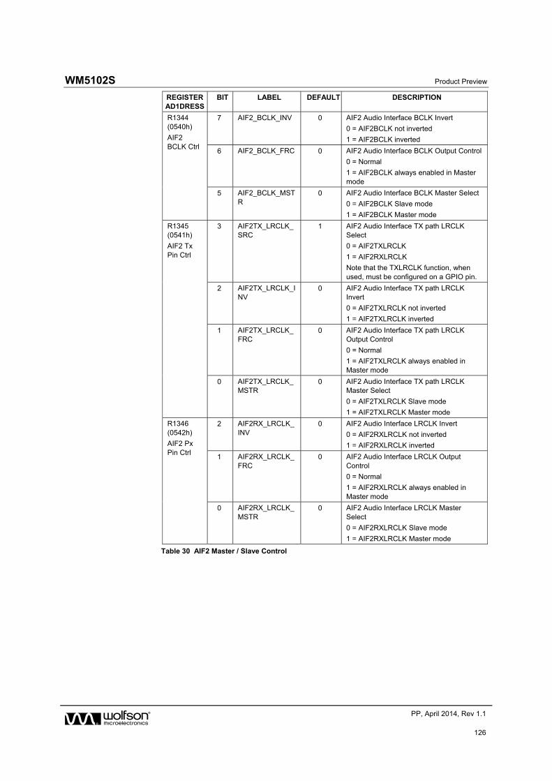
WM5102S Product Preview
w PP, April 2014, Rev 1.1
126
REGISTER AD1DRESS
BIT LABEL DEFAULT DESCRIPTION
R1344 (0540h)
AIF2 BCLK Ctrl
7 AIF2_BCLK_INV 0 AIF2 Audio Interface BCLK Invert
0 = AIF2BCLK not inverted
1 = AIF2BCLK inverted
6 AIF2_BCLK_FRC 0 AIF2 Audio Interface BCLK Output Control
0 = Normal
1 = AIF2BCLK always enabled in Master mode
5 AIF2_BCLK_MSTR
0 AIF2 Audio Interface BCLK Master Select
0 = AIF2BCLK Slave mode
1 = AIF2BCLK Master mode
R1345 (0541h)
AIF2 Tx Pin Ctrl
3 AIF2TX_LRCLK_SRC
1 AIF2 Audio Interface TX path LRCLK Select
0 = AIF2TXLRCLK
1 = AIF2RXLRCLK
Note that the TXLRCLK function, when used, must be configured on a GPIO pin.
2 AIF2TX_LRCLK_INV
0 AIF2 Audio Interface TX path LRCLK Invert
0 = AIF2TXLRCLK not inverted
1 = AIF2TXLRCLK inverted
1 AIF2TX_LRCLK_FRC
0 AIF2 Audio Interface TX path LRCLK Output Control
0 = Normal
1 = AIF2TXLRCLK always enabled in Master mode
0 AIF2TX_LRCLK_MSTR
0 AIF2 Audio Interface TX path LRCLK Master Select
0 = AIF2TXLRCLK Slave mode
1 = AIF2TXLRCLK Master mode
R1346 (0542h)
AIF2 Px Pin Ctrl
2 AIF2RX_LRCLK_INV
0 AIF2 Audio Interface LRCLK Invert
0 = AIF2RXLRCLK not inverted
1 = AIF2RXLRCLK inverted
1 AIF2RX_LRCLK_FRC
0 AIF2 Audio Interface LRCLK Output Control
0 = Normal
1 = AIF2RXLRCLK always enabled in Master mode
0 AIF2RX_LRCLK_MSTR
0 AIF2 Audio Interface LRCLK Master Select
0 = AIF2RXLRCLK Slave mode
1 = AIF2RXLRCLK Master mode
Table 30 AIF2 Master / Slave Control

Product Preview WM5102S
w PP, April 2014, Rev 1.1
127
REGISTER ADDRESS
BIT LABEL DEFAULT DESCRIPTION
R1408 (0580h)
AIF3 BCLK Ctrl
7 AIF3_BCLK_INV 0 AIF3 Audio Interface BCLK Invert
0 = AIF3BCLK not inverted
1 = AIF3BCLK inverted
6 AIF3_BCLK_FRC 0 AIF3 Audio Interface BCLK Output Control
0 = Normal
1 = AIF3BCLK always enabled in Master mode
5 AIF3_BCLK_MSTR
0 AIF3 Audio Interface BCLK Master Select
0 = AIF3BCLK Slave mode
1 = AIF3BCLK Master mode
R1409 (0581h)
AIF3 Tx Pin Ctrl
3 AIF3TX_LRCLK_SRC
1 AIF3 Audio Interface TX path LRCLK Select
0 = AIF3TXLRCLK
1 = AIF3RXLRCLK
Note that the TXLRCLK function, when used, must be configured on a GPIO pin.
2 AIF3TX_LRCLK_INV
0 AIF3 Audio Interface TX path LRCLK Invert
0 = AIF3TXLRCLK not inverted
1 = AIF3TXLRCLK inverted
1 AIF3TX_LRCLK_FRC
0 AIF3 Audio Interface TX path LRCLK Output Control
0 = Normal
1 = AIF3TXLRCLK always enabled in Master mode
0 AIF3TX_LRCLK_MSTR
0 AIF3 Audio Interface TX path LRCLK Master Select
0 = AIF3TXLRCLK Slave mode
1 = AIF3TXLRCLK Master mode
R1410 (0582h)
AIF3 Rx Pin Ctrl
2 AIF3RX_LRCLK_INV
0 AIF3 Audio Interface LRCLK Invert
0 = AIF3RXLRCLK not inverted
1 = AIF3RXLRCLK inverted
1 AIF3RX_LRCLK_FRC
0 AIF3 Audio Interface LRCLK Output Control
0 = Normal
1 = AIF3RXLRCLK always enabled in Master mode
0 AIF3RX_LRCLK_MSTR
0 AIF3 Audio Interface LRCLK Master Select
0 = AIF3RXLRCLK Slave mode
1 = AIF3RXLRCLK Master mode
Table 31 AIF3 Master / Slave Control
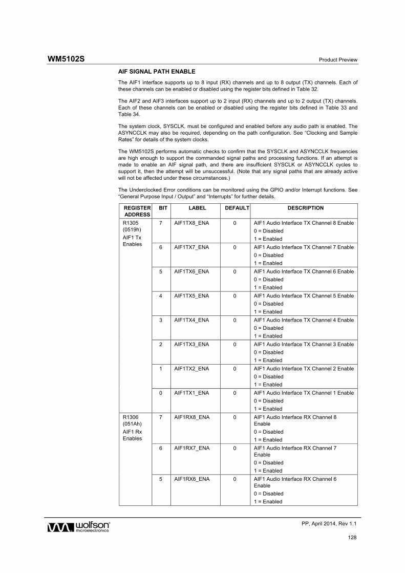
WM5102S Product Preview
w PP, April 2014, Rev 1.1
128
AIF SIGNAL PATH ENABLE
The AIF1 interface supports up to 8 input (RX) channels and up to 8 output (TX) channels. Each of these channels can be enabled or disabled using the register bits defined in Table 32.
The AIF2 and AIF3 interfaces support up to 2 input (RX) channels and up to 2 output (TX) channels. Each of these channels can be enabled or disabled using the register bits defined in Table 33 and Table 34.
The system clock, SYSCLK, must be configured and enabled before any audio path is enabled. The ASYNCCLK may also be required, depending on the path configuration. See “Clocking and Sample Rates” for details of the system clocks.
The WM5102S performs automatic checks to confirm that the SYSCLK and ASYNCCLK frequencies are high enough to support the commanded signal paths and processing functions. If an attempt is made to enable an AIF signal path, and there are insufficient SYSCLK or ASYNCCLK cycles to support it, then the attempt will be unsuccessful. (Note that any signal paths that are already active will not be affected under these circumstances.)
The Underclocked Error conditions can be monitored using the GPIO and/or Interrupt functions. See “General Purpose Input / Output” and “Interrupts” for further details.
REGISTER ADDRESS
BIT LABEL DEFAULT DESCRIPTION
R1305 (0519h)
AIF1 Tx Enables
7 AIF1TX8_ENA 0 AIF1 Audio Interface TX Channel 8 Enable
0 = Disabled
1 = Enabled
6 AIF1TX7_ENA 0 AIF1 Audio Interface TX Channel 7 Enable
0 = Disabled
1 = Enabled
5 AIF1TX6_ENA 0 AIF1 Audio Interface TX Channel 6 Enable
0 = Disabled
1 = Enabled
4 AIF1TX5_ENA 0 AIF1 Audio Interface TX Channel 5 Enable
0 = Disabled
1 = Enabled
3 AIF1TX4_ENA 0 AIF1 Audio Interface TX Channel 4 Enable
0 = Disabled
1 = Enabled
2 AIF1TX3_ENA 0 AIF1 Audio Interface TX Channel 3 Enable
0 = Disabled
1 = Enabled
1 AIF1TX2_ENA 0 AIF1 Audio Interface TX Channel 2 Enable
0 = Disabled
1 = Enabled
0 AIF1TX1_ENA 0 AIF1 Audio Interface TX Channel 1 Enable
0 = Disabled
1 = Enabled
R1306 (051Ah)
AIF1 Rx Enables
7 AIF1RX8_ENA 0 AIF1 Audio Interface RX Channel 8 Enable
0 = Disabled
1 = Enabled
6 AIF1RX7_ENA 0 AIF1 Audio Interface RX Channel 7 Enable
0 = Disabled
1 = Enabled
5 AIF1RX6_ENA 0 AIF1 Audio Interface RX Channel 6 Enable
0 = Disabled
1 = Enabled
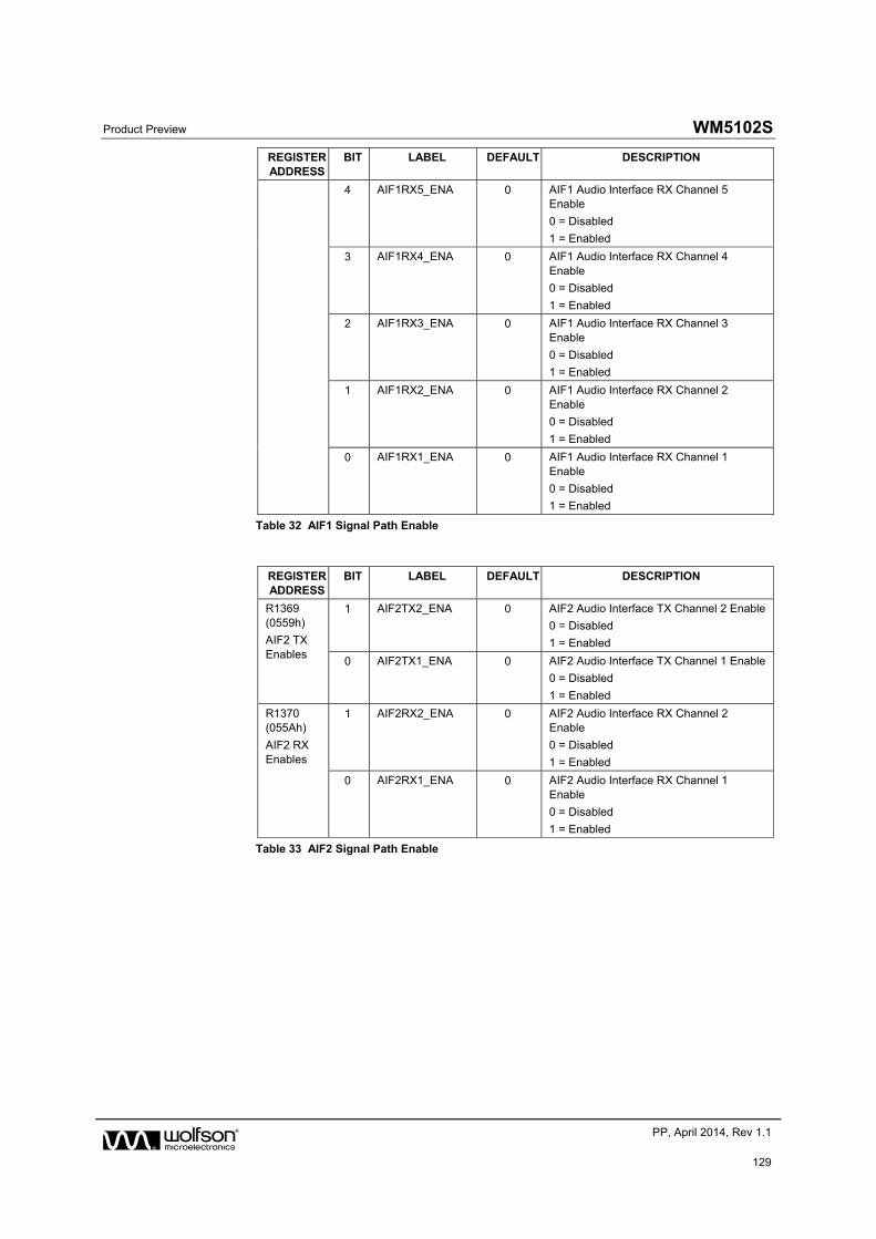
Product Preview WM5102S
w PP, April 2014, Rev 1.1
129
REGISTER ADDRESS
BIT LABEL DEFAULT DESCRIPTION
4 AIF1RX5_ENA 0 AIF1 Audio Interface RX Channel 5 Enable
0 = Disabled
1 = Enabled
3 AIF1RX4_ENA 0 AIF1 Audio Interface RX Channel 4 Enable
0 = Disabled
1 = Enabled
2 AIF1RX3_ENA 0 AIF1 Audio Interface RX Channel 3 Enable
0 = Disabled
1 = Enabled
1 AIF1RX2_ENA 0 AIF1 Audio Interface RX Channel 2 Enable
0 = Disabled
1 = Enabled
0 AIF1RX1_ENA 0 AIF1 Audio Interface RX Channel 1 Enable
0 = Disabled
1 = Enabled
Table 32 AIF1 Signal Path Enable
REGISTER ADDRESS
BIT LABEL DEFAULT DESCRIPTION
R1369 (0559h)
AIF2 TX Enables
1 AIF2TX2_ENA 0 AIF2 Audio Interface TX Channel 2 Enable
0 = Disabled
1 = Enabled
0 AIF2TX1_ENA 0 AIF2 Audio Interface TX Channel 1 Enable
0 = Disabled
1 = Enabled
R1370 (055Ah)
AIF2 RX Enables
1 AIF2RX2_ENA 0 AIF2 Audio Interface RX Channel 2 Enable
0 = Disabled
1 = Enabled
0 AIF2RX1_ENA 0 AIF2 Audio Interface RX Channel 1 Enable
0 = Disabled
1 = Enabled
Table 33 AIF2 Signal Path Enable
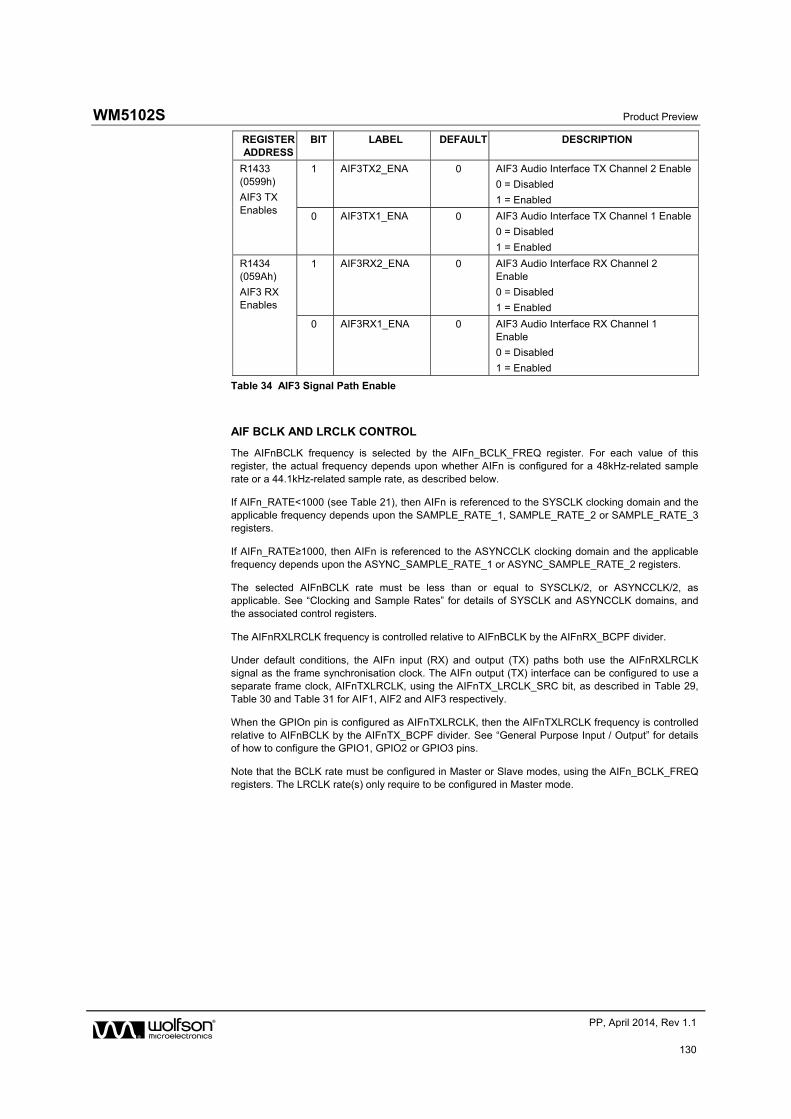
WM5102S Product Preview
w PP, April 2014, Rev 1.1
130
REGISTER ADDRESS
BIT LABEL DEFAULT DESCRIPTION
R1433 (0599h)
AIF3 TX Enables
1 AIF3TX2_ENA 0 AIF3 Audio Interface TX Channel 2 Enable
0 = Disabled
1 = Enabled
0 AIF3TX1_ENA 0 AIF3 Audio Interface TX Channel 1 Enable
0 = Disabled
1 = Enabled
R1434 (059Ah)
AIF3 RX Enables
1 AIF3RX2_ENA 0 AIF3 Audio Interface RX Channel 2 Enable
0 = Disabled
1 = Enabled
0 AIF3RX1_ENA 0 AIF3 Audio Interface RX Channel 1 Enable
0 = Disabled
1 = Enabled
Table 34 AIF3 Signal Path Enable
AIF BCLK AND LRCLK CONTROL
The AIFnBCLK frequency is selected by the AIFn_BCLK_FREQ register. For each value of this register, the actual frequency depends upon whether AIFn is configured for a 48kHz-related sample rate or a 44.1kHz-related sample rate, as described below.
If AIFn_RATE<1000 (see Table 21), then AIFn is referenced to the SYSCLK clocking domain and the applicable frequency depends upon the SAMPLE_RATE_1, SAMPLE_RATE_2 or SAMPLE_RATE_3 registers.
If AIFn_RATE≥1000, then AIFn is referenced to the ASYNCCLK clocking domain and the applicable frequency depends upon the ASYNC_SAMPLE_RATE_1 or ASYNC_SAMPLE_RATE_2 registers.
The selected AIFnBCLK rate must be less than or equal to SYSCLK/2, or ASYNCCLK/2, as applicable. See “Clocking and Sample Rates” for details of SYSCLK and ASYNCCLK domains, and the associated control registers.
The AIFnRXLRCLK frequency is controlled relative to AIFnBCLK by the AIFnRX_BCPF divider.
Under default conditions, the AIFn input (RX) and output (TX) paths both use the AIFnRXLRCLK signal as the frame synchronisation clock. The AIFn output (TX) interface can be configured to use a separate frame clock, AIFnTXLRCLK, using the AIFnTX_LRCLK_SRC bit, as described in Table 29, Table 30 and Table 31 for AIF1, AIF2 and AIF3 respectively.
When the GPIOn pin is configured as AIFnTXLRCLK, then the AIFnTXLRCLK frequency is controlled relative to AIFnBCLK by the AIFnTX_BCPF divider. See “General Purpose Input / Output” for details of how to configure the GPIO1, GPIO2 or GPIO3 pins.
Note that the BCLK rate must be configured in Master or Slave modes, using the AIFn_BCLK_FREQ registers. The LRCLK rate(s) only require to be configured in Master mode.
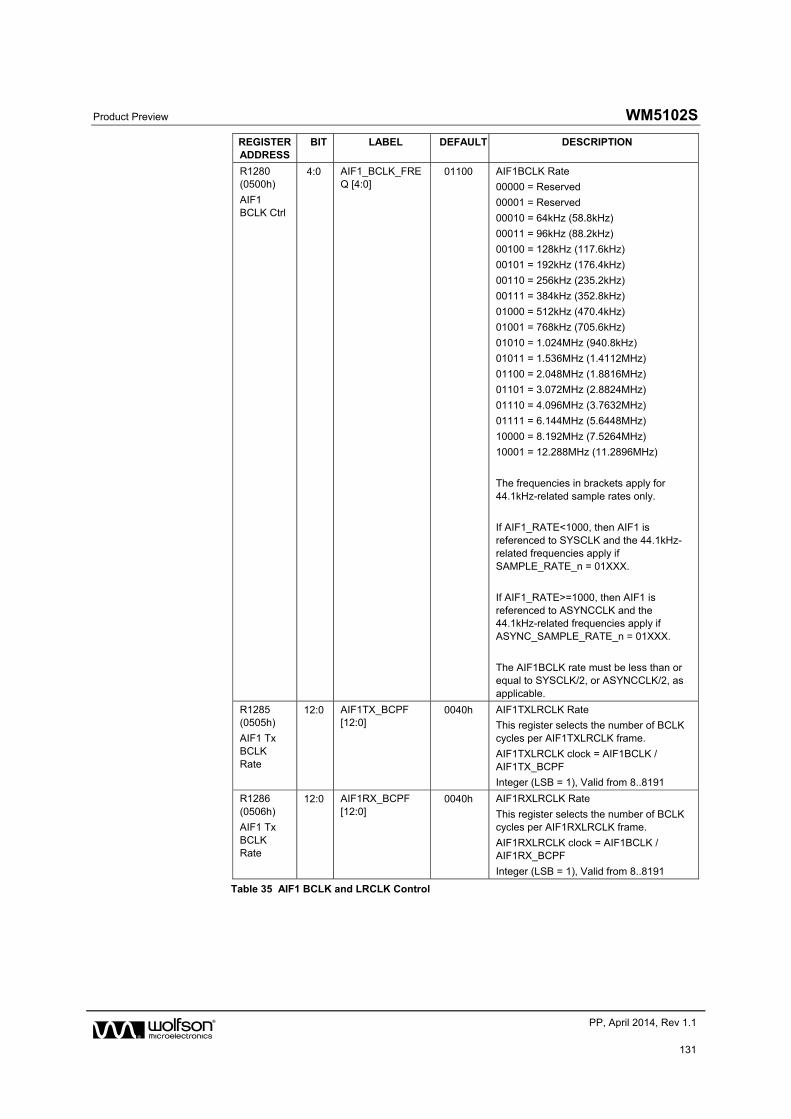
Product Preview WM5102S
w PP, April 2014, Rev 1.1
131
REGISTER ADDRESS
BIT LABEL DEFAULT DESCRIPTION
R1280 (0500h)
AIF1 BCLK Ctrl
4:0 AIF1_BCLK_FREQ [4:0]
01100 AIF1BCLK Rate
00000 = Reserved
00001 = Reserved
00010 = 64kHz (58.8kHz)
00011 = 96kHz (88.2kHz)
00100 = 128kHz (117.6kHz)
00101 = 192kHz (176.4kHz)
00110 = 256kHz (235.2kHz)
00111 = 384kHz (352.8kHz)
01000 = 512kHz (470.4kHz)
01001 = 768kHz (705.6kHz)
01010 = 1.024MHz (940.8kHz)
01011 = 1.536MHz (1.4112MHz)
01100 = 2.048MHz (1.8816MHz)
01101 = 3.072MHz (2.8824MHz)
01110 = 4.096MHz (3.7632MHz)
01111 = 6.144MHz (5.6448MHz)
10000 = 8.192MHz (7.5264MHz)
10001 = 12.288MHz (11.2896MHz)
The frequencies in brackets apply for 44.1kHz-related sample rates only.
If AIF1_RATE<1000, then AIF1 is referenced to SYSCLK and the 44.1kHz-related frequencies apply if SAMPLE_RATE_n = 01XXX.
If AIF1_RATE>=1000, then AIF1 is referenced to ASYNCCLK and the 44.1kHz-related frequencies apply if ASYNC_SAMPLE_RATE_n = 01XXX.
The AIF1BCLK rate must be less than or equal to SYSCLK/2, or ASYNCCLK/2, as applicable.
R1285 (0505h)
AIF1 Tx BCLK Rate
12:0 AIF1TX_BCPF [12:0]
0040h AIF1TXLRCLK Rate
This register selects the number of BCLK cycles per AIF1TXLRCLK frame.
AIF1TXLRCLK clock = AIF1BCLK / AIF1TX_BCPF
Integer (LSB = 1), Valid from 8..8191
R1286 (0506h)
AIF1 Tx BCLK Rate
12:0 AIF1RX_BCPF [12:0]
0040h AIF1RXLRCLK Rate
This register selects the number of BCLK cycles per AIF1RXLRCLK frame.
AIF1RXLRCLK clock = AIF1BCLK / AIF1RX_BCPF
Integer (LSB = 1), Valid from 8..8191
Table 35 AIF1 BCLK and LRCLK Control

WM5102S Product Preview
w PP, April 2014, Rev 1.1
132
REGISTER ADDRESS
BIT LABEL DEFAULT DESCRIPTION
R1344 (0540h)
AIF2 BCLK Ctrl
4:0 AIF2_BCLK_FREQ [4:0]
01100 AIF2BCLK Rate
00000 = Reserved
00001 = Reserved
00010 = 64kHz (58.8kHz)
00011 = 96kHz (88.2kHz)
00100 = 128kHz (117.6kHz)
00101 = 192kHz (176.4kHz)
00110 = 256kHz (235.2kHz)
00111 = 384kHz (352.8kHz)
01000 = 512kHz (470.4kHz)
01001 = 768kHz (705.6kHz)
01010 = 1.024MHz (940.8kHz)
01011 = 1.536MHz (1.4112MHz)
01100 = 2.048MHz (1.8816MHz)
01101 = 3.072MHz (2.8824MHz)
01110 = 4.096MHz (3.7632MHz)
01111 = 6.144MHz (5.6448MHz)
10000 = 8.192MHz (7.5264MHz)
10001 = 12.288MHz (11.2896MHz)
The frequencies in brackets apply for 44.1kHz-related sample rates only.
If AIF2_RATE<1000, then AIF2 is referenced to SYSCLK and the 44.1kHz-related frequencies apply if SAMPLE_RATE_n = 01XXX.
If AIF2_RATE>=1000, then AIF2 is referenced to ASYNCCLK and the 44.1kHz-related frequencies apply if ASYNC_SAMPLE_RATE_n = 01XXX.
The AIF2BCLK rate must be less than or equal to SYSCLK/2, or ASYNCCLK/2, as applicable.
R1349 (0545h)
AIF2 Tx BCLK Rate
12:0 AIF2TX_BCPF [12:0]
0040h AIF2TXLRCLK Rate
This register selects the number of BCLK cycles per AIF2TXLRCLK frame.
AIF2TXLRCLK clock = AIF2BCLK / AIF2TX_BCPF
Integer (LSB = 1), Valid from 8..8191
R1350 (0546h)
AIF2 Rx BCLK Rate
12:0 AIF2RX_BCPF [12:0]
0040h AIF2RXLRCLK Rate
This register selects the number of BCLK cycles per AIF2RXLRCLK frame.
AIF2RXLRCLK clock = AIF2BCLK / AIF2RX_BCPF
Integer (LSB = 1), Valid from 8..8191
Table 36 AIF2 BCLK and LRCLK Control
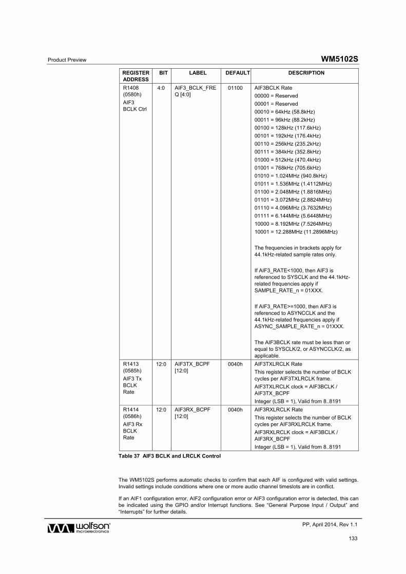
Product Preview WM5102S
w PP, April 2014, Rev 1.1
133
REGISTER ADDRESS
BIT LABEL DEFAULT DESCRIPTION
R1408 (0580h)
AIF3 BCLK Ctrl
4:0 AIF3_BCLK_FREQ [4:0]
01100 AIF3BCLK Rate
00000 = Reserved
00001 = Reserved
00010 = 64kHz (58.8kHz)
00011 = 96kHz (88.2kHz)
00100 = 128kHz (117.6kHz)
00101 = 192kHz (176.4kHz)
00110 = 256kHz (235.2kHz)
00111 = 384kHz (352.8kHz)
01000 = 512kHz (470.4kHz)
01001 = 768kHz (705.6kHz)
01010 = 1.024MHz (940.8kHz)
01011 = 1.536MHz (1.4112MHz)
01100 = 2.048MHz (1.8816MHz)
01101 = 3.072MHz (2.8824MHz)
01110 = 4.096MHz (3.7632MHz)
01111 = 6.144MHz (5.6448MHz)
10000 = 8.192MHz (7.5264MHz)
10001 = 12.288MHz (11.2896MHz)
The frequencies in brackets apply for 44.1kHz-related sample rates only.
If AIF3_RATE<1000, then AIF3 is referenced to SYSCLK and the 44.1kHz-related frequencies apply if SAMPLE_RATE_n = 01XXX.
If AIF3_RATE>=1000, then AIF3 is referenced to ASYNCCLK and the 44.1kHz-related frequencies apply if ASYNC_SAMPLE_RATE_n = 01XXX.
The AIF3BCLK rate must be less than or equal to SYSCLK/2, or ASYNCCLK/2, as applicable.
R1413 (0585h)
AIF3 Tx BCLK Rate
12:0 AIF3TX_BCPF [12:0]
0040h AIF3TXLRCLK Rate
This register selects the number of BCLK cycles per AIF3TXLRCLK frame.
AIF3TXLRCLK clock = AIF3BCLK / AIF3TX_BCPF
Integer (LSB = 1), Valid from 8..8191
R1414 (0586h)
AIF3 Rx BCLK Rate
12:0 AIF3RX_BCPF [12:0]
0040h AIF3RXLRCLK Rate
This register selects the number of BCLK cycles per AIF3RXLRCLK frame.
AIF3RXLRCLK clock = AIF3BCLK / AIF3RX_BCPF
Integer (LSB = 1), Valid from 8..8191
Table 37 AIF3 BCLK and LRCLK Control
The WM5102S performs automatic checks to confirm that each AIF is configured with valid settings. Invalid settings include conditions where one or more audio channel timeslots are in conflict.
If an AIF1 configuration error, AIF2 configuration error or AIF3 configuration error is detected, this can be indicated using the GPIO and/or Interrupt functions. See “General Purpose Input / Output” and “Interrupts” for further details.
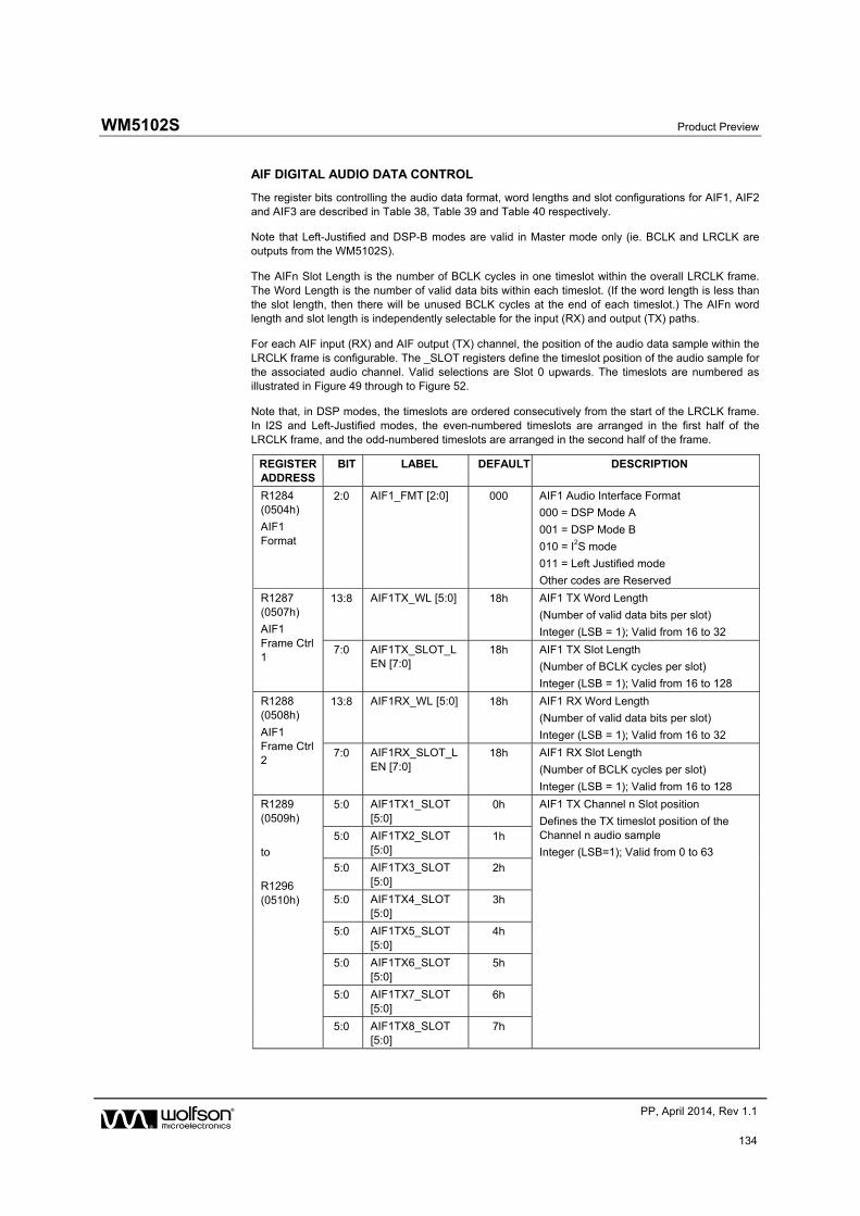
WM5102S Product Preview
w PP, April 2014, Rev 1.1
134
AIF DIGITAL AUDIO DATA CONTROL
The register bits controlling the audio data format, word lengths and slot configurations for AIF1, AIF2 and AIF3 are described in Table 38, Table 39 and Table 40 respectively.
Note that Left-Justified and DSP-B modes are valid in Master mode only (ie. BCLK and LRCLK are outputs from the WM5102S).
The AIFn Slot Length is the number of BCLK cycles in one timeslot within the overall LRCLK frame. The Word Length is the number of valid data bits within each timeslot. (If the word length is less than the slot length, then there will be unused BCLK cycles at the end of each timeslot.) The AIFn word length and slot length is independently selectable for the input (RX) and output (TX) paths.
For each AIF input (RX) and AIF output (TX) channel, the position of the audio data sample within the LRCLK frame is configurable. The _SLOT registers define the timeslot position of the audio sample for the associated audio channel. Valid selections are Slot 0 upwards. The timeslots are numbered as illustrated in Figure 49 through to Figure 52.
Note that, in DSP modes, the timeslots are ordered consecutively from the start of the LRCLK frame. In I2S and Left-Justified modes, the even-numbered timeslots are arranged in the first half of the LRCLK frame, and the odd-numbered timeslots are arranged in the second half of the frame.
REGISTER ADDRESS
BIT LABEL DEFAULT DESCRIPTION
R1284 (0504h)
AIF1 Format
2:0 AIF1_FMT [2:0] 000 AIF1 Audio Interface Format
000 = DSP Mode A
001 = DSP Mode B
010 = I2S mode
011 = Left Justified mode
Other codes are Reserved
R1287 (0507h)
AIF1 Frame Ctrl 1
13:8 AIF1TX_WL [5:0] 18h AIF1 TX Word Length
(Number of valid data bits per slot)
Integer (LSB = 1); Valid from 16 to 32
7:0 AIF1TX_SLOT_LEN [7:0]
18h AIF1 TX Slot Length
(Number of BCLK cycles per slot)
Integer (LSB = 1); Valid from 16 to 128
R1288 (0508h)
AIF1 Frame Ctrl 2
13:8 AIF1RX_WL [5:0] 18h AIF1 RX Word Length
(Number of valid data bits per slot)
Integer (LSB = 1); Valid from 16 to 32
7:0 AIF1RX_SLOT_LEN [7:0]
18h AIF1 RX Slot Length
(Number of BCLK cycles per slot)
Integer (LSB = 1); Valid from 16 to 128
R1289 (0509h)
to
R1296 (0510h)
5:0 AIF1TX1_SLOT [5:0]
0h AIF1 TX Channel n Slot position
Defines the TX timeslot position of the Channel n audio sample
Integer (LSB=1); Valid from 0 to 63
5:0 AIF1TX2_SLOT [5:0]
1h
5:0 AIF1TX3_SLOT [5:0]
2h
5:0 AIF1TX4_SLOT [5:0]
3h
5:0 AIF1TX5_SLOT [5:0]
4h
5:0 AIF1TX6_SLOT [5:0]
5h
5:0 AIF1TX7_SLOT [5:0]
6h
5:0 AIF1TX8_SLOT [5:0]
7h
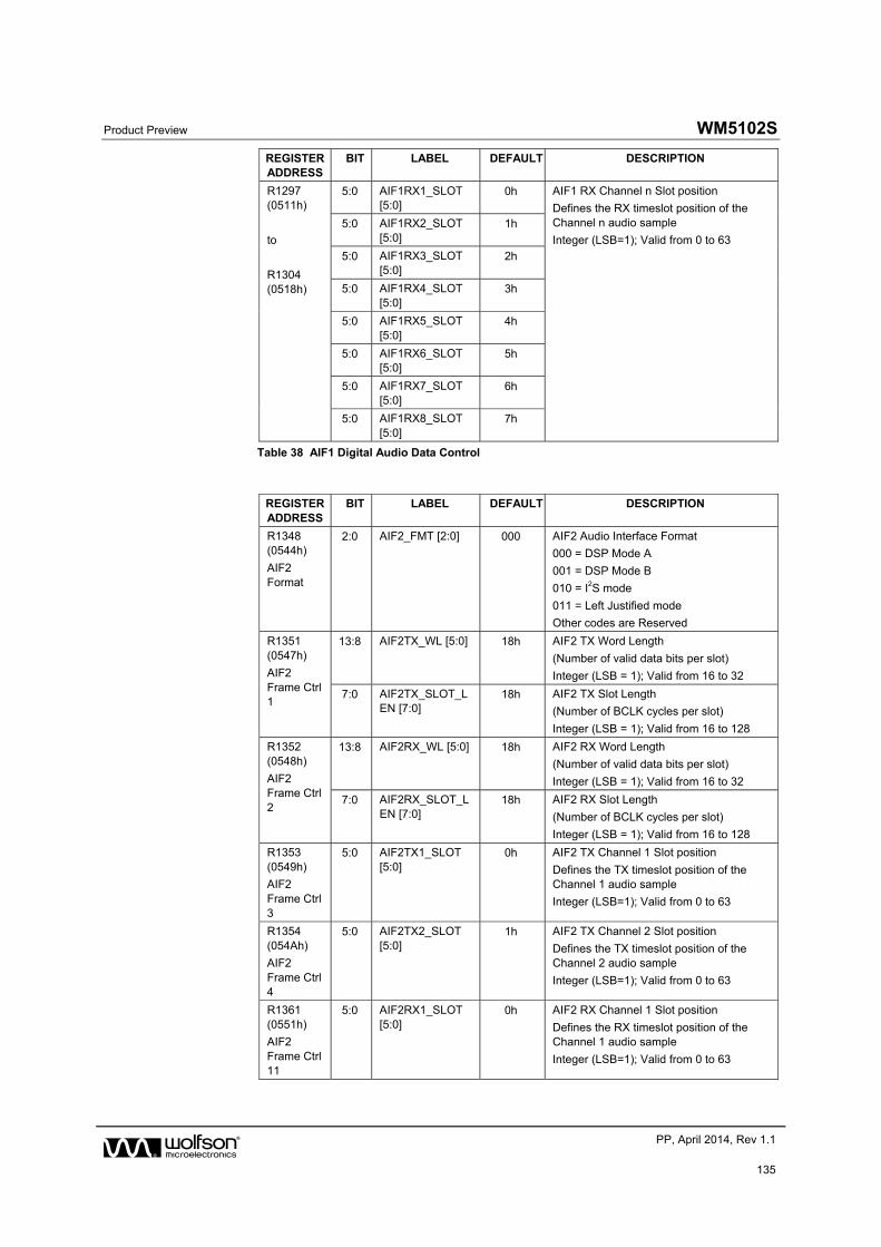
Product Preview WM5102S
w PP, April 2014, Rev 1.1
135
REGISTER ADDRESS
BIT LABEL DEFAULT DESCRIPTION
R1297 (0511h)
to
R1304 (0518h)
5:0 AIF1RX1_SLOT [5:0]
0h AIF1 RX Channel n Slot position
Defines the RX timeslot position of the Channel n audio sample
Integer (LSB=1); Valid from 0 to 63
5:0 AIF1RX2_SLOT [5:0]
1h
5:0 AIF1RX3_SLOT [5:0]
2h
5:0 AIF1RX4_SLOT [5:0]
3h
5:0 AIF1RX5_SLOT [5:0]
4h
5:0 AIF1RX6_SLOT [5:0]
5h
5:0 AIF1RX7_SLOT [5:0]
6h
5:0 AIF1RX8_SLOT [5:0]
7h
Table 38 AIF1 Digital Audio Data Control
REGISTER ADDRESS
BIT LABEL DEFAULT DESCRIPTION
R1348 (0544h)
AIF2 Format
2:0 AIF2_FMT [2:0] 000 AIF2 Audio Interface Format
000 = DSP Mode A
001 = DSP Mode B
010 = I2S mode
011 = Left Justified mode
Other codes are Reserved
R1351 (0547h)
AIF2 Frame Ctrl 1
13:8 AIF2TX_WL [5:0] 18h AIF2 TX Word Length
(Number of valid data bits per slot)
Integer (LSB = 1); Valid from 16 to 32
7:0 AIF2TX_SLOT_LEN [7:0]
18h AIF2 TX Slot Length
(Number of BCLK cycles per slot)
Integer (LSB = 1); Valid from 16 to 128
R1352 (0548h)
AIF2 Frame Ctrl 2
13:8 AIF2RX_WL [5:0] 18h AIF2 RX Word Length
(Number of valid data bits per slot)
Integer (LSB = 1); Valid from 16 to 32
7:0 AIF2RX_SLOT_LEN [7:0]
18h AIF2 RX Slot Length
(Number of BCLK cycles per slot)
Integer (LSB = 1); Valid from 16 to 128
R1353 (0549h)
AIF2 Frame Ctrl 3
5:0 AIF2TX1_SLOT [5:0]
0h AIF2 TX Channel 1 Slot position
Defines the TX timeslot position of the Channel 1 audio sample
Integer (LSB=1); Valid from 0 to 63
R1354 (054Ah)
AIF2 Frame Ctrl 4
5:0 AIF2TX2_SLOT [5:0]
1h AIF2 TX Channel 2 Slot position
Defines the TX timeslot position of the Channel 2 audio sample
Integer (LSB=1); Valid from 0 to 63
R1361 (0551h)
AIF2 Frame Ctrl 11
5:0 AIF2RX1_SLOT [5:0]
0h AIF2 RX Channel 1 Slot position
Defines the RX timeslot position of the Channel 1 audio sample
Integer (LSB=1); Valid from 0 to 63
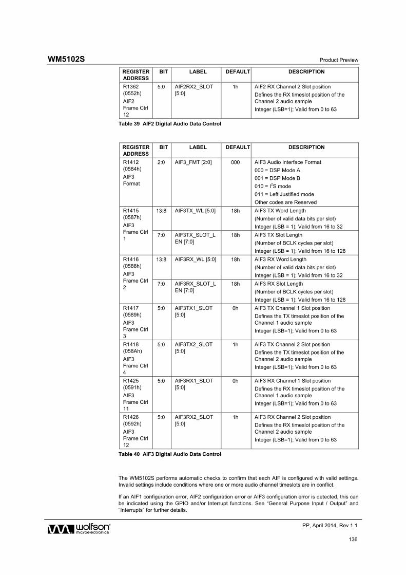
WM5102S Product Preview
w PP, April 2014, Rev 1.1
136
REGISTER ADDRESS
BIT LABEL DEFAULT DESCRIPTION
R1362 (0552h)
AIF2 Frame Ctrl 12
5:0 AIF2RX2_SLOT [5:0]
1h AIF2 RX Channel 2 Slot position
Defines the RX timeslot position of the Channel 2 audio sample
Integer (LSB=1); Valid from 0 to 63
Table 39 AIF2 Digital Audio Data Control
REGISTER ADDRESS
BIT LABEL DEFAULT DESCRIPTION
R1412 (0584h)
AIF3 Format
2:0 AIF3_FMT [2:0] 000 AIF3 Audio Interface Format
000 = DSP Mode A
001 = DSP Mode B
010 = I2S mode
011 = Left Justified mode
Other codes are Reserved
R1415 (0587h)
AIF3 Frame Ctrl 1
13:8 AIF3TX_WL [5:0] 18h AIF3 TX Word Length
(Number of valid data bits per slot)
Integer (LSB = 1); Valid from 16 to 32
7:0 AIF3TX_SLOT_LEN [7:0]
18h AIF3 TX Slot Length
(Number of BCLK cycles per slot)
Integer (LSB = 1); Valid from 16 to 128
R1416 (0588h)
AIF3 Frame Ctrl 2
13:8 AIF3RX_WL [5:0] 18h AIF3 RX Word Length
(Number of valid data bits per slot)
Integer (LSB = 1); Valid from 16 to 32
7:0 AIF3RX_SLOT_LEN [7:0]
18h AIF3 RX Slot Length
(Number of BCLK cycles per slot)
Integer (LSB = 1); Valid from 16 to 128
R1417 (0589h)
AIF3 Frame Ctrl 3
5:0 AIF3TX1_SLOT [5:0]
0h AIF3 TX Channel 1 Slot position
Defines the TX timeslot position of the Channel 1 audio sample
Integer (LSB=1); Valid from 0 to 63
R1418 (058Ah)
AIF3 Frame Ctrl 4
5:0 AIF3TX2_SLOT [5:0]
1h AIF3 TX Channel 2 Slot position
Defines the TX timeslot position of the Channel 2 audio sample
Integer (LSB=1); Valid from 0 to 63
R1425 (0591h)
AIF3 Frame Ctrl 11
5:0 AIF3RX1_SLOT [5:0]
0h AIF3 RX Channel 1 Slot position
Defines the RX timeslot position of the Channel 1 audio sample
Integer (LSB=1); Valid from 0 to 63
R1426 (0592h)
AIF3 Frame Ctrl 12
5:0 AIF3RX2_SLOT [5:0]
1h AIF3 RX Channel 2 Slot position
Defines the RX timeslot position of the Channel 2 audio sample
Integer (LSB=1); Valid from 0 to 63
Table 40 AIF3 Digital Audio Data Control
The WM5102S performs automatic checks to confirm that each AIF is configured with valid settings. Invalid settings include conditions where one or more audio channel timeslots are in conflict.
If an AIF1 configuration error, AIF2 configuration error or AIF3 configuration error is detected, this can be indicated using the GPIO and/or Interrupt functions. See “General Purpose Input / Output” and “Interrupts” for further details.
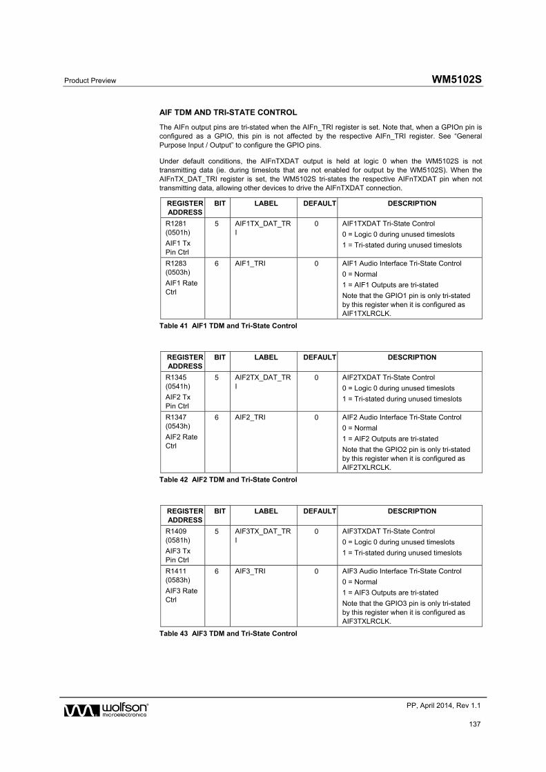
Product Preview WM5102S
w PP, April 2014, Rev 1.1
137
AIF TDM AND TRI-STATE CONTROL
The AIFn output pins are tri-stated when the AIFn_TRI register is set. Note that, when a GPIOn pin is configured as a GPIO, this pin is not affected by the respective AIFn_TRI register. See “General Purpose Input / Output” to configure the GPIO pins.
Under default conditions, the AIFnTXDAT output is held at logic 0 when the WM5102S is not transmitting data (ie. during timeslots that are not enabled for output by the WM5102S). When the AIFnTX_DAT_TRI register is set, the WM5102S tri-states the respective AIFnTXDAT pin when not transmitting data, allowing other devices to drive the AIFnTXDAT connection.
REGISTER ADDRESS
BIT LABEL DEFAULT DESCRIPTION
R1281 (0501h)
AIF1 Tx Pin Ctrl
5 AIF1TX_DAT_TRI
0 AIF1TXDAT Tri-State Control
0 = Logic 0 during unused timeslots
1 = Tri-stated during unused timeslots
R1283 (0503h)
AIF1 Rate Ctrl
6 AIF1_TRI 0 AIF1 Audio Interface Tri-State Control
0 = Normal
1 = AIF1 Outputs are tri-stated
Note that the GPIO1 pin is only tri-stated by this register when it is configured as AIF1TXLRCLK.
Table 41 AIF1 TDM and Tri-State Control
REGISTER ADDRESS
BIT LABEL DEFAULT DESCRIPTION
R1345 (0541h)
AIF2 Tx Pin Ctrl
5 AIF2TX_DAT_TRI
0 AIF2TXDAT Tri-State Control
0 = Logic 0 during unused timeslots
1 = Tri-stated during unused timeslots
R1347 (0543h)
AIF2 Rate Ctrl
6 AIF2_TRI 0 AIF2 Audio Interface Tri-State Control
0 = Normal
1 = AIF2 Outputs are tri-stated
Note that the GPIO2 pin is only tri-stated by this register when it is configured as AIF2TXLRCLK.
Table 42 AIF2 TDM and Tri-State Control
REGISTER ADDRESS
BIT LABEL DEFAULT DESCRIPTION
R1409 (0581h)
AIF3 Tx Pin Ctrl
5 AIF3TX_DAT_TRI
0 AIF3TXDAT Tri-State Control
0 = Logic 0 during unused timeslots
1 = Tri-stated during unused timeslots
R1411 (0583h)
AIF3 Rate Ctrl
6 AIF3_TRI 0 AIF3 Audio Interface Tri-State Control
0 = Normal
1 = AIF3 Outputs are tri-stated
Note that the GPIO3 pin is only tri-stated by this register when it is configured as AIF3TXLRCLK.
Table 43 AIF3 TDM and Tri-State Control
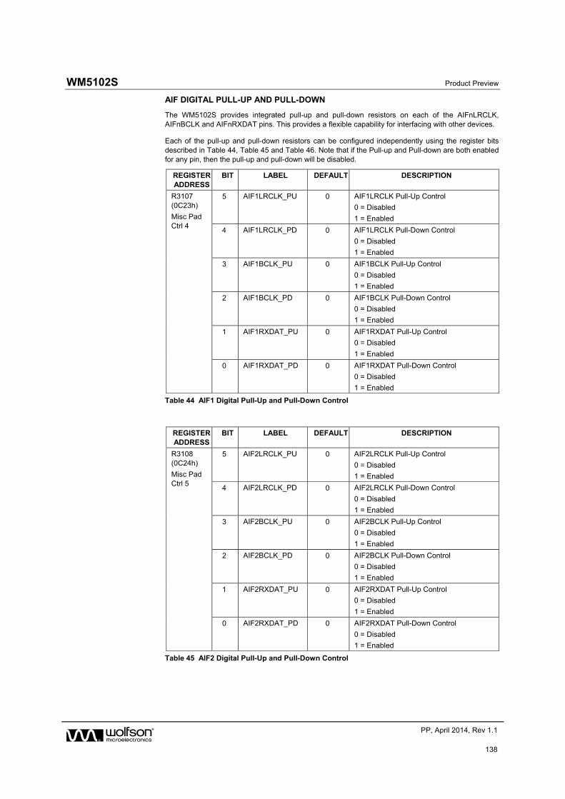
WM5102S Product Preview
w PP, April 2014, Rev 1.1
138
AIF DIGITAL PULL-UP AND PULL-DOWN
The WM5102S provides integrated pull-up and pull-down resistors on each of the AIFnLRCLK, AIFnBCLK and AIFnRXDAT pins. This provides a flexible capability for interfacing with other devices.
Each of the pull-up and pull-down resistors can be configured independently using the register bits described in Table 44, Table 45 and Table 46. Note that if the Pull-up and Pull-down are both enabled for any pin, then the pull-up and pull-down will be disabled.
REGISTER ADDRESS
BIT LABEL DEFAULT DESCRIPTION
R3107 (0C23h)
Misc Pad Ctrl 4
5 AIF1LRCLK_PU 0 AIF1LRCLK Pull-Up Control
0 = Disabled
1 = Enabled
4 AIF1LRCLK_PD 0 AIF1LRCLK Pull-Down Control
0 = Disabled
1 = Enabled
3 AIF1BCLK_PU 0 AIF1BCLK Pull-Up Control
0 = Disabled
1 = Enabled
2 AIF1BCLK_PD 0 AIF1BCLK Pull-Down Control
0 = Disabled
1 = Enabled
1 AIF1RXDAT_PU 0 AIF1RXDAT Pull-Up Control
0 = Disabled
1 = Enabled
0 AIF1RXDAT_PD 0 AIF1RXDAT Pull-Down Control
0 = Disabled
1 = Enabled
Table 44 AIF1 Digital Pull-Up and Pull-Down Control
REGISTER ADDRESS
BIT LABEL DEFAULT DESCRIPTION
R3108 (0C24h)
Misc Pad Ctrl 5
5 AIF2LRCLK_PU 0 AIF2LRCLK Pull-Up Control
0 = Disabled
1 = Enabled
4 AIF2LRCLK_PD 0 AIF2LRCLK Pull-Down Control
0 = Disabled
1 = Enabled
3 AIF2BCLK_PU 0 AIF2BCLK Pull-Up Control
0 = Disabled
1 = Enabled
2 AIF2BCLK_PD 0 AIF2BCLK Pull-Down Control
0 = Disabled
1 = Enabled
1 AIF2RXDAT_PU 0 AIF2RXDAT Pull-Up Control
0 = Disabled
1 = Enabled
0 AIF2RXDAT_PD 0 AIF2RXDAT Pull-Down Control
0 = Disabled
1 = Enabled
Table 45 AIF2 Digital Pull-Up and Pull-Down Control
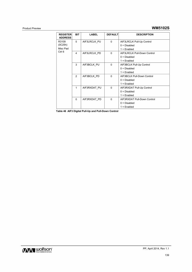
Product Preview WM5102S
w PP, April 2014, Rev 1.1
139
REGISTER ADDRESS
BIT LABEL DEFAULT DESCRIPTION
R3109 (0C25h)
Misc Pad Ctrl 6
5 AIF3LRCLK_PU 0 AIF3LRCLK Pull-Up Control
0 = Disabled
1 = Enabled
4 AIF3LRCLK_PD 0 AIF3LRCLK Pull-Down Control
0 = Disabled
1 = Enabled
3 AIF3BCLK_PU 0 AIF3BCLK Pull-Up Control
0 = Disabled
1 = Enabled
2 AIF3BCLK_PD 0 AIF3BCLK Pull-Down Control
0 = Disabled
1 = Enabled
1 AIF3RXDAT_PU 0 AIF3RXDAT Pull-Up Control
0 = Disabled
1 = Enabled
0 AIF3RXDAT_PD 0 AIF3RXDAT Pull-Down Control
0 = Disabled
1 = Enabled
Table 46 AIF3 Digital Pull-Up and Pull-Down Control
WM5102S Product Preview
w PP, April 2014, Rev 1.1
140
SLIMBUS INTERFACE
The SLIMbus protocol is highly configurable and adaptable, supporting multiple audio signal paths, and mixed sample rates simultaneously. It also supports control messaging and associated communications between devices.
SLIMBUS DEVICES
The SLIMbus components comprise different device classes (Manager, Framer, Interface, Generic). Each component on the bus has an Interface Device, which provides bus management services for the respective component. One or more components on the bus will provide Manager and Framer Device functions; the Manager has the capabilities to administer the bus, whilst the Framer is responsible for driving the CLK line and for driving the DATA required to establish the Frame Structure on the bus. Note that only one Manager and one Framer Device will be active at any time. The Framer function can be transferred between Devices when required. Generic Devices provide the basic SLIMbus functionality for the associated Port(s), and for the Transport Protocol by which audio signal paths are established on the bus.
SLIMBUS FRAME STRUCTURE
The SLIMbus bit stream is formatted within a defined structure of Cells, Slots, Subframes, Frames, and Superframes:
A single data bit is known as a Cell
4 Cells make a Slot
192 Slots make a Frame
8 Frames make a Superframe
The bit stream structure is configurable to some extent, but the Superframe definition always comprises 1536 slots. The transmitted/received bit rate is not fixed; it can be configured according to system requirements, and can be changed dynamically without interruption to active audio paths.
The SLIMbus CLK frequency (also the bus bit rate) is defined by a Root Frequency (RF) and a Clock Gear (CG). In the top Clock Gear (Gear 10), the CLK frequency is equal to the Root Frequency. Each reduction in the Clock Gear halves the CLK frequency, and doubles the duration of the Superframe.
The SLIMbus bandwidth will typically comprise Control space (for bus messages, synchronisation etc.) and Data space (for audio paths). The precise allocation is configurable, and can be entirely Control space, if required.
The Subframe definition comprises the number of Slots per Subframe (6, 8, 24 or 32 Slots), and the number of these Slots (per Subframe) allocated as Control space. The applicable combination of Subframe length and Control space width are defined by the Subframe Mode (SM) parameter.
The SLIMbus Frame always comprises 192 Slots, regardless of the Subframe definition. A number of Slots are allocated to Control space, as noted above; the remaining Slots are allocated to Data space. Some of the Control space is required for Framing Information and for the Guide Channel (described below); the remainder of the Control space are allocated to the Message Channel.
CONTROL SPACE
Framing Information is provided in Slots 0 and 96 of every Frame. Slot 0 contains a 4-bit synchronisation code; Slot 96 contains the 32-bit Framing Information, transmitted 4 bits at a time over the 8 Frames that make up the SLIMbus Superframe. The Clock Gear, Root Frequency, Subframe configuration, along with some other parameters, are encoded within the Framing Information.
Product Preview WM5102S
w PP, April 2014, Rev 1.1
141
The Guide Channel occupies two Slots within Frame 0. This provides the necessary information for a SLIMbus component to acquire and verify the frame synchronisation. The Guide Channel occupies the first two Control space Slots within the first Frame of the bit stream, excluding the Framing Information Slots. Note that the exact Slot allocation will depend upon the applicable Subframe mode.
The Message Channel is allocated all of the Control space not used by the Framing Information or the Guide Channel. The Message Channel enables SLIMbus devices to communicate with each other, using a priority-based mechanism defined in the MIPI specification.
Messages may be broadcast to all devices on the bus, or can be addressed to specific devices using their allocated Logical Address (LA) or Enumeration Address (EA). Note that, device-specific messages are directed to a particular device (ie. Manager, Framer, Interface or Generic) within a component on the bus.
DATA SPACE
The Data space can be organised into a maximum of 256 Data Channels. Each Channel, identified by a unique Channel Number (CN), is a stream of one or more contiguous Slots, organised in a consistent data structure that repeats at a fixed interval.
A Data Channel is defined by its Segment Length (SL) (number of contiguous Slots allocated), Segment Interval (spacing between the first Slots of successive Segments), and Segment Offset (the Slot Number of the first allocated Slot within the Superframe). The Segment Interval and Segment Offset are collectively defined by a Segment Distribution (SD), by which the SLIMbus Manager may configure (or re-configure) any Data Channel.
Each Segment may comprise TAG, AUX and DATA portions. Any of these portions may be 0-length; the exact composition depends on the Transport Protocol (TP) for the associated Channel (see below). The DATA portion must be wide enough to accommodate one full word of the Data Channel contents (data words cannot be spread across multiple segments).
The Segment Interval for each Data Channel represents the minimum spacing between consecutive data samples for that Channel. (Note - the minimum spacing applies if every allocated segment is populated with new data; in many cases, additional bandwidth is allocated, as described below, and not every allocated segment is used.)
The Segment Interval gives rise to Segment Windows for each Data Channel, aligned to the start of every Superframe. The Segment Window boundaries define the times within which each new data sample must be buffered, ready for transmission - adherence to these fixed boundaries allows Slot allocations to be moved within a Segment Window, without altering the signal latency. The Segment Interval may be either shorter or longer than the Frame length, but there is always an integer number of Segment Windows per Superframe.
The Transport Protocol (TP) defines the flow control or handshaking method used by the Ports associated with a Data Channel. The applicable flow control mode(s) depend on the relationship between the audio sample rate (flow rate) and the SLIMbus CLK frequency. If the two rates are synchronised and integer-related, then no flow control is needed; in other cases, the flow may be regulated by the use of a ‘Presence’ bit. The Presence bit can either be set by the source Device (‘pushed’ protocol), or by the sink Device (‘pulled’ protocol).
The Data Channel structure is defined in terms of the Transport Protocol (TP), Segment Distribution (SD), and the Segment Length (SL) parameters. Each of these is described above.
The Data Channel content definition includes a Presence Rate (PR) parameter (describing the nominal sample rate for the audio channel) and a Frequency Locked (FL) bit (identifying whether the data source is synchronised to the SLIMbus CLK). The Data Length (DL) parameter defines the size of each data sample (number of Slots). The Auxiliary Bits Format (AF) and Data Type (DT) parameters provide support for non-PCM encoded data channels; the Channel Link (CL) parameter is an indicator that channel CN is related to the previous channel, CN-1.
For a given Root Frequency and Clock Gear, the Segment Length (SL) and Segment Distribution (SD) parameters define the amount of SLIMbus bandwidth that is allocated to a given Data Channel. The minimum bandwidth requirements of a Data Channel are represented by the Presence Rate (PR) and Data Length (DL) parameters. The allocated SLIMbus bandwidth must be equal to or greater than the bandwidth of the data to be transferred.
WM5102S Product Preview
w PP, April 2014, Rev 1.1
142
The Segment Interval (see above), defines the repetition rate of the SLIMbus Slots allocated to consecutive data samples for a given Data Channel. The Presence Rate (PR) is the nominal sample rate of the audio path. The Segment Interval must be equal to or greater than the Presence Rate for a given Data Channel.
In some applications, the allocated SLIMbus bandwidth must be greater than the data rate, to ensure that samples are not dropped as a result of clock drift etc. The SLIMbus bandwidth should only be set equal to the data rate if the data source is frequency-locked to the SLIMbus CLK (ie. the data source is synchronised to the SLIMbus Framer device).
SLIMBUS CONTROL SEQUENCES
This section describes the messages and general protocol associated with most aspects of the SLIMbus system.
Note that the SLIMbus specification permits some flexibility in Core Message support for different components. See “SLIMbus Interface Control” for details of which message(s) are supported on each of the SLIMbus devices that are present on the WM5102S.
DEVICE MANAGEMENT & CONFIGURATION
This section describes the SLIMbus messages associated with configuring all devices on the SLIMbus interface.
When the SLIMbus interface starts up, it is required that one (and only one) of the components provides the Manager and Framer Device functions. Other devices can request connection to the bus after they have gained synchronisation.
The REPORT_PRESENT (DC, DCV) message may be issued by devices attempting to connect to the bus. The payload of this message contains the Device Class (DC) and Device Class Version (DCV) parameters, describing the type of device that is attempting to connect. This message may be issued autonomously by the connecting device, or else in response to a REQUEST_SELF_ANNOUNCEMENT message from the Manager Device.
After positively acknowledging the REPORT_PRESENT message, the Manager Device will then issue the ASSIGN_LOGICAL_ADDRESS (LA) message to allow the other device to connect to the bus. The payload of this message contains the Logical Address (LA) parameter only; this is the unique address by which the connected device will send and receive SLIMbus messages. The device is then said to be ‘enumerated’.
Once a device has been successfully connected to the bus, the Logical Address (LA) parameter can be changed at any time using the CHANGE_LOGICAL_ADDRESS (LA) message.
The RESET_DEVICE message commands an individual SLIMbus device to perform its reset procedure. As part of the reset, all associated ports will be reset, and any associated Data Channels will be cancelled. Note that, if the RESET_DEVICE command is issued to an Interface Device, it will cause a Component Reset (ie. all Devices within the associated component are reset). Under a Component Reset, every associated Device will release its Logical Address, and the Component will become disconnected from the bus.
INFORMATION MANAGEMENT
A memory map of Information Elements is defined for each Device. This is arranged in 3 x 1kByte blocks, as described in the MIPI specification.
Read/Write access is implemented using the messages described below. Specific elements within the Information Map are identified using the Element Code (EC) parameter. In the case of Read access, a unique Transaction ID (TID) is assigned to each message relating to a particular read/write request.
The REQUEST_INFORMATION (TID, EC) message is used to instruct a device to respond with the indicated information. The payload of this message contains the Transaction ID (TID) and the Element Code (EC).
Product Preview WM5102S
w PP, April 2014, Rev 1.1
143
The REQUEST_CLEAR_INFORMATION (TID, EC, CM) message is used to instruct a device to respond with the indicated information, and also to clear all, or parts, of the same information slice. The payload of this message contains the Transaction ID (TID), Element Code (EC), and Clear Mask (CM). The Clear Mask field is used to select which element(s) are to be cleared as part of the instruction.
The REPLY_INFORMATION (TID, IS) message is used to provide readback of a requested parameter. The payload of this message contains the Transaction ID (TID) and the Information Slice (IS). The Information Slice byte(s) contain the value of the requested parameter.
The CLEAR_INFORMATION (EC, CM) message is used to clear all, or parts, of the indicated information slice. The payload of this message contains the Element Code (EC) and Clear Mask (CM). The Clear Mask field is used to select which element(s) are to be cleared as part of the instruction.
The REPORT_INFORMATION (EC, IS) message is used to inform other devices about a change in a specified element in the Information Map. The payload of this message contains the Element Code (EC) and the Information Slice (IS). The Information Slice byte(s) contain the new value of the applicable parameter.
VALUE MANAGEMENT (INCLUDING REGISTER ACCESS)
A memory map of Value Elements is defined for each Device. This is arranged in 3 x 1kByte blocks, as described in the MIPI specification. These elements are typically parameters used to configure Device behaviour.
The User Value Elements space within the Value Map are used on WM5102S to support Read/Write access to the Register Map. Details of how to access specific registers are described in the “SLIMbus Interface Control” section.
Read/Write access is implemented using the messages described below. Specific elements within the Value Map are identified using the Element Code (EC) parameter. In the case of Read access, a unique Transaction ID (TID) is assigned to each message relating to a particular read/write request.
The REQUEST_VALUE (TID, EC) message is used to instruct a device to respond with the indicated information. The payload of this message contains the Transaction ID (TID) and the Element Code (EC).
The REPLY_VALUE (TID, VS) message is used to provide readback of a requested parameter. The payload of this message contains the Transaction ID (TID) and the Value Slice (VS). The Value Slice byte(s) contain the value of the requested parameter.
The CHANGE_VALUE (EC, VU) message is used to write data to a specified element in the Value Map. The payload of this message contains the Element Code (EC) and the Value Update (VU). The Value Update byte(s) contain the new value of the applicable parameter.
FRAME & CLOCKING MANAGEMENT
This section describes the SLIMbus messages associated with changing the Frame or Clocking configuration. One or more configuration messages may be issued as part of a Reconfiguration Sequence; all of the updated parameters become active at once, when the Reconfiguration boundary is reached.
The BEGIN_RECONFIGURATION message is issued to define a Reconfiguration Boundary point: subsequent NEXT_* messages will become active at the first valid Superframe boundary following receipt of the RECONFIGURE_NOW message. (A valid boundary must be at least two Slots after the end of the RECONFIGURE_NOW message.) Both of these messages have no payload content.
The NEXT_ACTIVE_FRAMER (LAIF, NCo, NCi) message is used to select a new device as the active Framer. The payload of this message includes the Logical Address, Incoming Framer (LAIF). Two other fields (NCo, NCi) define the number of clock cycles for which the CLK line shall be inactive during the handover.
The NEXT_SUBFRAME_MODE (SM) and NEXT_CLOCK_GEAR (CG) messages are used to re-configure the SLIMbus clocking or framing definition. The payload of each is the respective Subframe Mode (SM) or Clock Gear (CG) respectively.
The NEXT_PAUSE_CLOCK (RT) message instructs the active Framer to pause the bus. The payload
WM5102S Product Preview
w PP, April 2014, Rev 1.1
144
of the message contains the Restart Time (RT), which indicates whether the interruption is to be of a specified time and/or phase duration.
The NEXT_RESET_BUS message instructs all components on the bus to be reset. In this case, all Devices on the bus are reset and are disconnected from the bus. Subsequent re-connection to the bus follows the same process as when the bus is first initialised.
The NEXT_SHUTDOWN_BUS message instructs all devices that the bus is to be shut down.
DATA CHANNEL CONFIGURATION
This section describes the procedure for configuring a SLIMbus Data Channel. Note that the Manager Device is responsible for allocating the available bandwidth as required for each Data Channel.
The CONNECT_SOURCE (PN, CN) and CONNECT_SINK (PN, CN) messages are issued to the respective devices, defining the Port(s) between which a Data Channel is to be established. Note that multiple destinations (sinks) can be configured for a channel, if required. The payload of each message contains the Port Number (PN) and the Channel Number (CN) parameters.
The BEGIN_RECONFIGURATION message is issued to define a Reconfiguration Boundary point: subsequent NEXT_* messages will become active at the first valid Superframe boundary following receipt of the RECONFIGURE_NOW message. (A valid boundary must be at least two Slots after the end of the RECONFIGURE_NOW message.)
The NEXT_DEFINE_CHANNEL (CN, TP, SD, SL) message informs the associated devices of the structure of the Data Channel. The payload of this message contains the Channel Number (CN), Transport Protocol (TP), Segment Distribution (SD), and the Segment Length (SL) parameters for the Data Channel.
The NEXT_DEFINE_CONTENT (CN, FL, PR, AF, DT, CL, DL), or CHANGE_CONTENT (CN, FL, PR, AF, DT, CL, DL) message provides more detailed information about the Data Channel contents. The payload of this message contains the Channel Number (CN), Frequency Locked (FL), Presence Rate (PR), Auxiliary Bits Format (AF), Data Type (DT), Channel Link (CL), and Data Length (DL) parameters.
The NEXT_ACTIVATE_CHANNEL (CN) message instructs the channel to be activated at the next Reconfiguration boundary. The payload of this message contains the Channel Number (CN) only.
The RECONFIGURE_NOW message completes the Reconfiguration sequence, causing all of the ‘NEXT_’ messages since the BEGIN_RECONFIGURATION to become active at the next valid Superframe boundary. (A valid boundary must be at least two Slots after the end of the RECONFIGURE_NOW message.)
Active channels can be reconfigured using the CHANGE_CONTENT, NEXT_DEFINE_CONTENT, or NEXT_DEFINE_CHANNEL messages. Note that these changes can be effected without interrupting the data channel; the NEXT_DEFINE_CHANNEL, for example, may be used to change a Segment Distribution, in order to reallocate the SLIMbus bandwidth.
An active channel can be paused using the NEXT_DEACTIVATE_CHANNEL message, and re-instated using the NEXT_ACTIVATE_CHANNEL message.
Data channels can be disconnected using the DISCONNECT_PORT or NEXT_REMOVE_CHANNEL messages. These messages provide equivalent functionality, but use different parameters (PN or CN respectively) to identify the affected signal path.
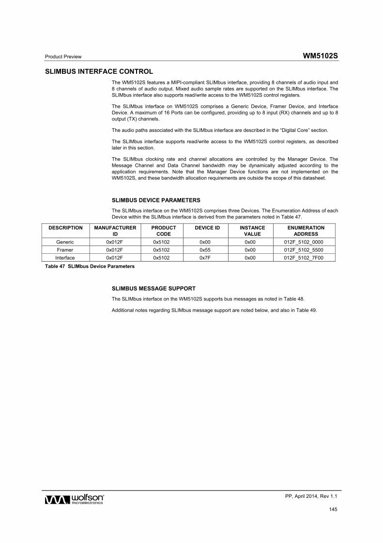
Product Preview WM5102S
w PP, April 2014, Rev 1.1
145
SLIMBUS INTERFACE CONTROL
The WM5102S features a MIPI-compliant SLIMbus interface, providing 8 channels of audio input and 8 channels of audio output. Mixed audio sample rates are supported on the SLIMbus interface. The SLIMbus interface also supports read/write access to the WM5102S control registers.
The SLIMbus interface on WM5102S comprises a Generic Device, Framer Device, and Interface Device. A maximum of 16 Ports can be configured, providing up to 8 input (RX) channels and up to 8 output (TX) channels.
The audio paths associated with the SLIMbus interface are described in the “Digital Core” section.
The SLIMbus interface supports read/write access to the WM5102S control registers, as described later in this section.
The SLIMbus clocking rate and channel allocations are controlled by the Manager Device. The Message Channel and Data Channel bandwidth may be dynamically adjusted according to the application requirements. Note that the Manager Device functions are not implemented on the WM5102S, and these bandwidth allocation requirements are outside the scope of this datasheet.
SLIMBUS DEVICE PARAMETERS
The SLIMbus interface on the WM5102S comprises three Devices. The Enumeration Address of each Device within the SLIMbus interface is derived from the parameters noted in Table 47.
DESCRIPTION MANUFACTURER ID
PRODUCT CODE
DEVICE ID INSTANCE VALUE
ENUMERATION ADDRESS
Generic 0x012F 0x5102 0x00 0x00 012F_5102_0000
Framer 0x012F 0x5102 0x55 0x00 012F_5102_5500
Interface 0x012F 0x5102 0x7F 0x00 012F_5102_7F00
Table 47 SLIMbus Device Parameters
SLIMBUS MESSAGE SUPPORT
The SLIMbus interface on the WM5102S supports bus messages as noted in Table 48.
Additional notes regarding SLIMbus message support are noted below, and also in Table 49.
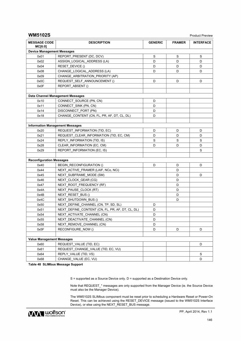
WM5102S Product Preview
w PP, April 2014, Rev 1.1
146
MESSAGE CODE MC[6:0]
DESCRIPTION GENERIC FRAMER INTERFACE
Device Management Messages
0x01 REPORT_PRESENT (DC, DCV) S S S
0x02 ASSIGN_LOGICAL_ADDRESS (LA) D D D
0x04 RESET_DEVICE () D D D
0x08 CHANGE_LOGICAL_ADDRESS (LA) D D D
0x09 CHANGE_ARBITRATION_PRIORITY (AP)
0x0C REQUEST_SELF_ANNOUNCEMENT () D D D
0x0F REPORT_ABSENT ()
Data Channel Management Messages
0x10 CONNECT_SOURCE (PN, CN) D
0x11 CONNECT_SINK (PN, CN) D
0x14 DISCONNECT_PORT (PN) D
0x18 CHANGE_CONTENT (CN, FL, PR, AF, DT, CL, DL) D
Information Management Messages
0x20 REQUEST_INFORMATION (TID, EC) D D D
0x21 REQUEST_CLEAR_INFORMATION (TID, EC, CM) D D D
0x24 REPLY_INFORMATION (TID, IS) S S S
0x28 CLEAR_INFORMATION (EC, CM) D D D
0x29 REPORT_INFORMATION (EC, IS) S
Reconfiguration Messages
0x40 BEGIN_RECONFIGURATION () D D D
0x44 NEXT_ACTIVE_FRAMER (LAIF, NCo, NCi) D
0x45 NEXT_SUBFRAME_MODE (SM) D D
0x46 NEXT_CLOCK_GEAR (CG) D
0x47 NEXT_ROOT_FREQUENCY (RF) D
0x4A NEXT_PAUSE_CLOCK (RT) D
0x4B NEXT_RESET_BUS () D
0x4C NEXT_SHUTDOWN_BUS () D
0x50 NEXT_DEFINE_CHANNEL (CN, TP, SD, SL) D
0x51 NEXT_DEFINE_CONTENT (CN, FL, PR, AF, DT, CL, DL) D
0x54 NEXT_ACTIVATE_CHANNEL (CN) D
0x55 NEXT_DEACTIVATE_CHANNEL (CN) D
0x58 NEXT_REMOVE_CHANNEL (CN) D
0x5F RECONFIGURE_NOW () D D D
Value Management Messages
0x60 REQUEST_VALUE (TID, EC) D
0x61 REQUEST_CHANGE_VALUE (TID, EC, VU)
0x64 REPLY_VALUE (TID, VS) S
0x68 CHANGE_VALUE (EC, VU) D
Table 48 SLIMbus Message Support
S = supported as a Source Device only. D = supported as a Destination Device only.
Note that REQUEST_* messages are only supported from the Manager Device (ie. the Source Device must also be the Manager Device).
The WM5102S SLIMbus component must be reset prior to scheduling a Hardware Reset or Power-On Reset. This can be achieved using the RESET_DEVICE message (issued to the WM5102S Interface Device), or else using the NEXT_RESET_BUS message.
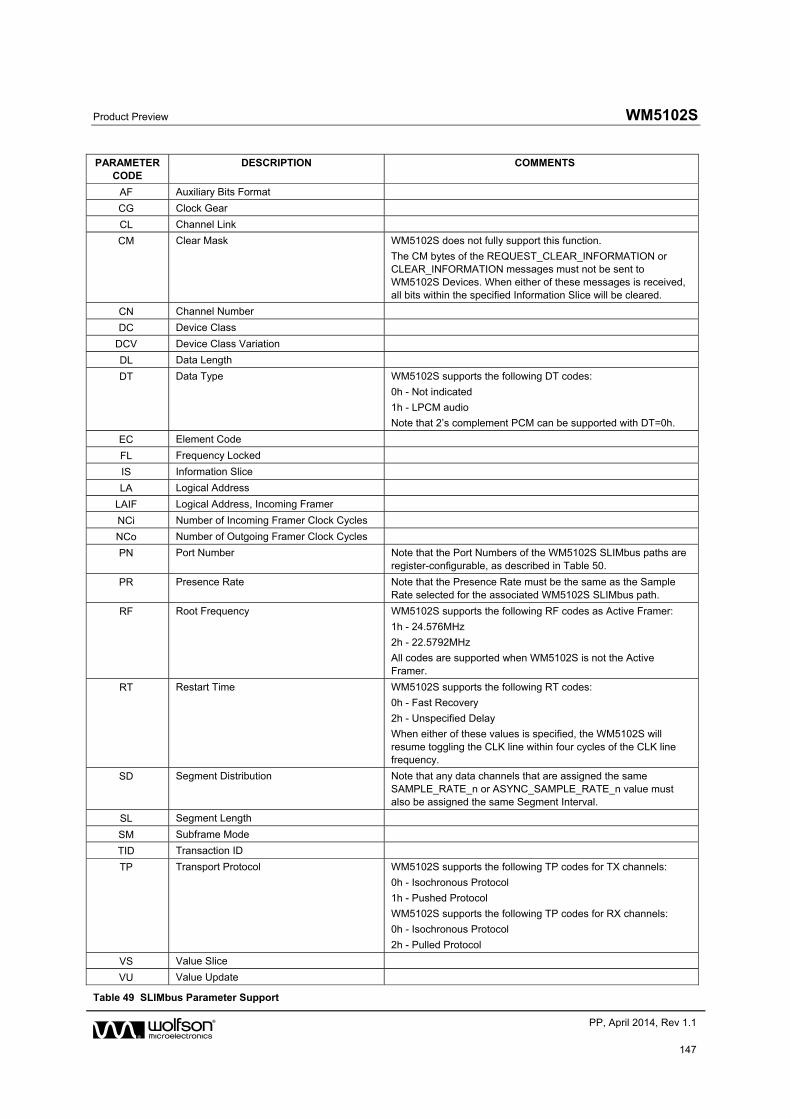
Product Preview WM5102S
w PP, April 2014, Rev 1.1
147
PARAMETER CODE
DESCRIPTION COMMENTS
AF Auxiliary Bits Format
CG Clock Gear
CL Channel Link
CM Clear Mask WM5102S does not fully support this function.
The CM bytes of the REQUEST_CLEAR_INFORMATION or CLEAR_INFORMATION messages must not be sent to WM5102S Devices. When either of these messages is received, all bits within the specified Information Slice will be cleared.
CN Channel Number
DC Device Class
DCV Device Class Variation
DL Data Length
DT Data Type WM5102S supports the following DT codes:
0h - Not indicated
1h - LPCM audio
Note that 2’s complement PCM can be supported with DT=0h.
EC Element Code
FL Frequency Locked
IS Information Slice
LA Logical Address
LAIF Logical Address, Incoming Framer
NCi Number of Incoming Framer Clock Cycles
NCo Number of Outgoing Framer Clock Cycles
PN Port Number Note that the Port Numbers of the WM5102S SLIMbus paths are register-configurable, as described in Table 50.
PR Presence Rate Note that the Presence Rate must be the same as the Sample Rate selected for the associated WM5102S SLIMbus path.
RF Root Frequency WM5102S supports the following RF codes as Active Framer:
1h - 24.576MHz
2h - 22.5792MHz
All codes are supported when WM5102S is not the Active Framer.
RT Restart Time WM5102S supports the following RT codes:
0h - Fast Recovery
2h - Unspecified Delay
When either of these values is specified, the WM5102S will resume toggling the CLK line within four cycles of the CLK line frequency.
SD Segment Distribution Note that any data channels that are assigned the same SAMPLE_RATE_n or ASYNC_SAMPLE_RATE_n value must also be assigned the same Segment Interval.
SL Segment Length
SM Subframe Mode
TID Transaction ID
TP Transport Protocol WM5102S supports the following TP codes for TX channels:
0h - Isochronous Protocol
1h - Pushed Protocol
WM5102S supports the following TP codes for RX channels:
0h - Isochronous Protocol
2h - Pulled Protocol
VS Value Slice
VU Value Update
Table 49 SLIMbus Parameter Support
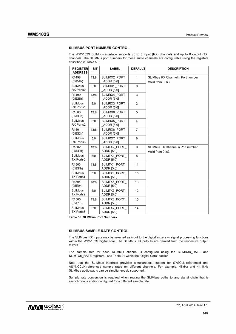
WM5102S Product Preview
w PP, April 2014, Rev 1.1
148
SLIMBUS PORT NUMBER CONTROL
The WM5102S SLIMbus interface supports up to 8 input (RX) channels and up to 8 output (TX) channels. The SLIMbus port numbers for these audio channels are configurable using the registers described in Table 50.
REGISTER ADDRESS
BIT LABEL DEFAULT DESCRIPTION
R1498 (05DAh)
SLIMbus RX Ports0
13:8 SLIMRX2_PORT_ADDR [5:0]
1 SLIMbus RX Channel n Port number
Valid from 0..63 5:0 SLIMRX1_PORT
_ADDR [5:0] 0
R1499 (05DBh)
SLIMbus RX Ports1
13:8 SLIMRX4_PORT_ADDR [5:0]
3
5:0 SLIMRX3_PORT_ADDR [5:0]
2
R1500 (05DCh)
SLIMbus RX Ports2
13:8 SLIMRX6_PORT_ADDR [5:0]
5
5:0 SLIMRX5_PORT_ADDR [5:0]
4
R1501 (05DDh)
SLIMbus RX Ports3
13:8 SLIMRX8_PORT_ADDR [5:0]
7
5:0 SLIMRX7_PORT_ADDR [5:0]
6
R1502 (05DEh)
SLIMbus TX Ports0
13:8 SLIMTX2_PORT_ADDR [5:0]
9 SLIMbus TX Channel n Port number
Valid from 0..63 5:0 SLIMTX1_PORT_
ADDR [5:0] 8
R1503 (05DFh)
SLIMbus TX Ports1
13:8 SLIMTX4_PORT_ADDR [5:0]
11
5:0 SLIMTX3_PORT_ADDR [5:0]
10
R1504 (05E0h)
SLIMbus TX Ports2
13:8 SLIMTX6_PORT_ADDR [5:0]
13
5:0 SLIMTX5_PORT_ADDR [5:0]
12
R1505 (05E1h)
SLIMbus TX Ports3
13:8 SLIMTX8_PORT_ADDR [5:0]
15
5:0 SLIMTX7_PORT_ADDR [5:0]
14
Table 50 SLIMbus Port Numbers
SLIMBUS SAMPLE RATE CONTROL
The SLIMbus RX inputs may be selected as input to the digital mixers or signal processing functions within the WM5102S digital core. The SLIMbus TX outputs are derived from the respective output mixers.
The sample rate for each SLIMbus channel is configured using the SLIMRXn_RATE and SLIMTXn_RATE registers - see Table 21 within the “Digital Core” section.
Note that the SLIMbus interface provides simultaneous support for SYSCLK-referenced and ASYNCCLK-referenced sample rates on different channels. For example, 48kHz and 44.1kHz SLIMbus audio paths can be simultaneously supported.
Sample rate conversion is required when routing the SLIMbus paths to any signal chain that is asynchronous and/or configured for a different sample rate.
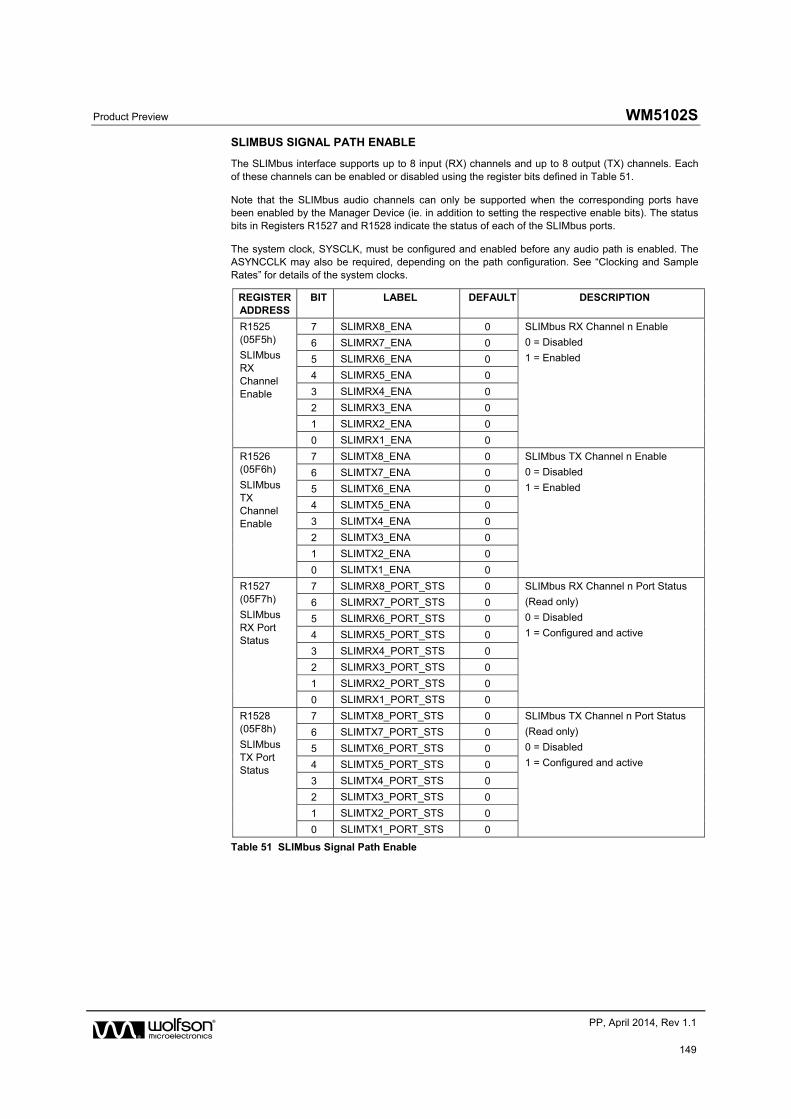
Product Preview WM5102S
w PP, April 2014, Rev 1.1
149
SLIMBUS SIGNAL PATH ENABLE
The SLIMbus interface supports up to 8 input (RX) channels and up to 8 output (TX) channels. Each of these channels can be enabled or disabled using the register bits defined in Table 51.
Note that the SLIMbus audio channels can only be supported when the corresponding ports have been enabled by the Manager Device (ie. in addition to setting the respective enable bits). The status bits in Registers R1527 and R1528 indicate the status of each of the SLIMbus ports.
The system clock, SYSCLK, must be configured and enabled before any audio path is enabled. The ASYNCCLK may also be required, depending on the path configuration. See “Clocking and Sample Rates” for details of the system clocks.
REGISTER ADDRESS
BIT LABEL DEFAULT DESCRIPTION
R1525 (05F5h)
SLIMbus RX Channel Enable
7 SLIMRX8_ENA 0 SLIMbus RX Channel n Enable
0 = Disabled
1 = Enabled
6 SLIMRX7_ENA 0
5 SLIMRX6_ENA 0
4 SLIMRX5_ENA 0
3 SLIMRX4_ENA 0
2 SLIMRX3_ENA 0
1 SLIMRX2_ENA 0
0 SLIMRX1_ENA 0
R1526 (05F6h)
SLIMbus TX Channel Enable
7 SLIMTX8_ENA 0 SLIMbus TX Channel n Enable
0 = Disabled
1 = Enabled
6 SLIMTX7_ENA 0
5 SLIMTX6_ENA 0
4 SLIMTX5_ENA 0
3 SLIMTX4_ENA 0
2 SLIMTX3_ENA 0
1 SLIMTX2_ENA 0
0 SLIMTX1_ENA 0
R1527 (05F7h)
SLIMbus RX Port Status
7 SLIMRX8_PORT_STS 0 SLIMbus RX Channel n Port Status
(Read only)
0 = Disabled
1 = Configured and active
6 SLIMRX7_PORT_STS 0
5 SLIMRX6_PORT_STS 0
4 SLIMRX5_PORT_STS 0
3 SLIMRX4_PORT_STS 0
2 SLIMRX3_PORT_STS 0
1 SLIMRX2_PORT_STS 0
0 SLIMRX1_PORT_STS 0
R1528 (05F8h)
SLIMbus TX Port Status
7 SLIMTX8_PORT_STS 0 SLIMbus TX Channel n Port Status
(Read only)
0 = Disabled
1 = Configured and active
6 SLIMTX7_PORT_STS 0
5 SLIMTX6_PORT_STS 0
4 SLIMTX5_PORT_STS 0
3 SLIMTX4_PORT_STS 0
2 SLIMTX3_PORT_STS 0
1 SLIMTX2_PORT_STS 0
0 SLIMTX1_PORT_STS 0
Table 51 SLIMbus Signal Path Enable
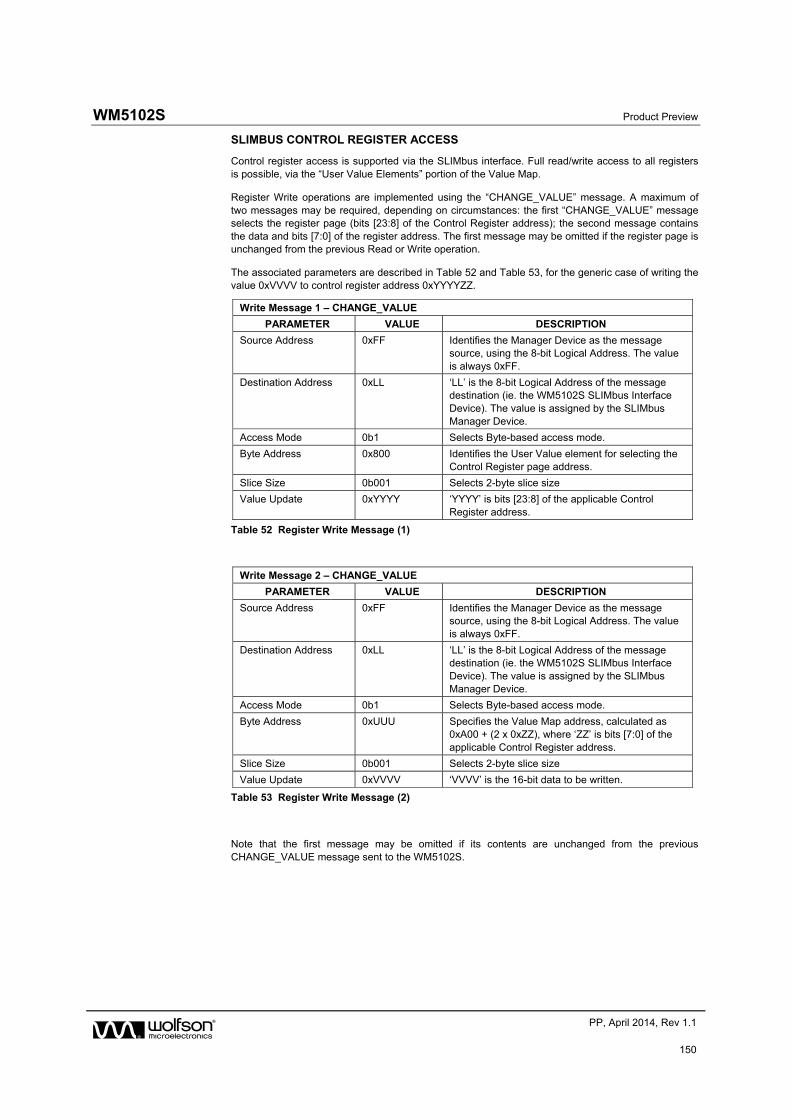
WM5102S Product Preview
w PP, April 2014, Rev 1.1
150
SLIMBUS CONTROL REGISTER ACCESS
Control register access is supported via the SLIMbus interface. Full read/write access to all registers is possible, via the “User Value Elements” portion of the Value Map.
Register Write operations are implemented using the “CHANGE_VALUE” message. A maximum of two messages may be required, depending on circumstances: the first “CHANGE_VALUE” message selects the register page (bits [23:8] of the Control Register address); the second message contains the data and bits [7:0] of the register address. The first message may be omitted if the register page is unchanged from the previous Read or Write operation.
The associated parameters are described in Table 52 and Table 53, for the generic case of writing the value 0xVVVV to control register address 0xYYYYZZ.
Write Message 1 – CHANGE_VALUE
PARAMETER VALUE DESCRIPTION
Source Address 0xFF Identifies the Manager Device as the message source, using the 8-bit Logical Address. The value is always 0xFF.
Destination Address 0xLL ‘LL’ is the 8-bit Logical Address of the message destination (ie. the WM5102S SLIMbus Interface Device). The value is assigned by the SLIMbus Manager Device.
Access Mode 0b1 Selects Byte-based access mode.
Byte Address 0x800 Identifies the User Value element for selecting the Control Register page address.
Slice Size 0b001 Selects 2-byte slice size
Value Update 0xYYYY ‘YYYY’ is bits [23:8] of the applicable Control Register address.
Table 52 Register Write Message (1)
Write Message 2 – CHANGE_VALUE
PARAMETER VALUE DESCRIPTION
Source Address 0xFF Identifies the Manager Device as the message source, using the 8-bit Logical Address. The value is always 0xFF.
Destination Address 0xLL ‘LL’ is the 8-bit Logical Address of the message destination (ie. the WM5102S SLIMbus Interface Device). The value is assigned by the SLIMbus Manager Device.
Access Mode 0b1 Selects Byte-based access mode.
Byte Address 0xUUU Specifies the Value Map address, calculated as 0xA00 + (2 x 0xZZ), where ‘ZZ’ is bits [7:0] of the applicable Control Register address.
Slice Size 0b001 Selects 2-byte slice size
Value Update 0xVVVV ‘VVVV’ is the 16-bit data to be written.
Table 53 Register Write Message (2)
Note that the first message may be omitted if its contents are unchanged from the previous CHANGE_VALUE message sent to the WM5102S.
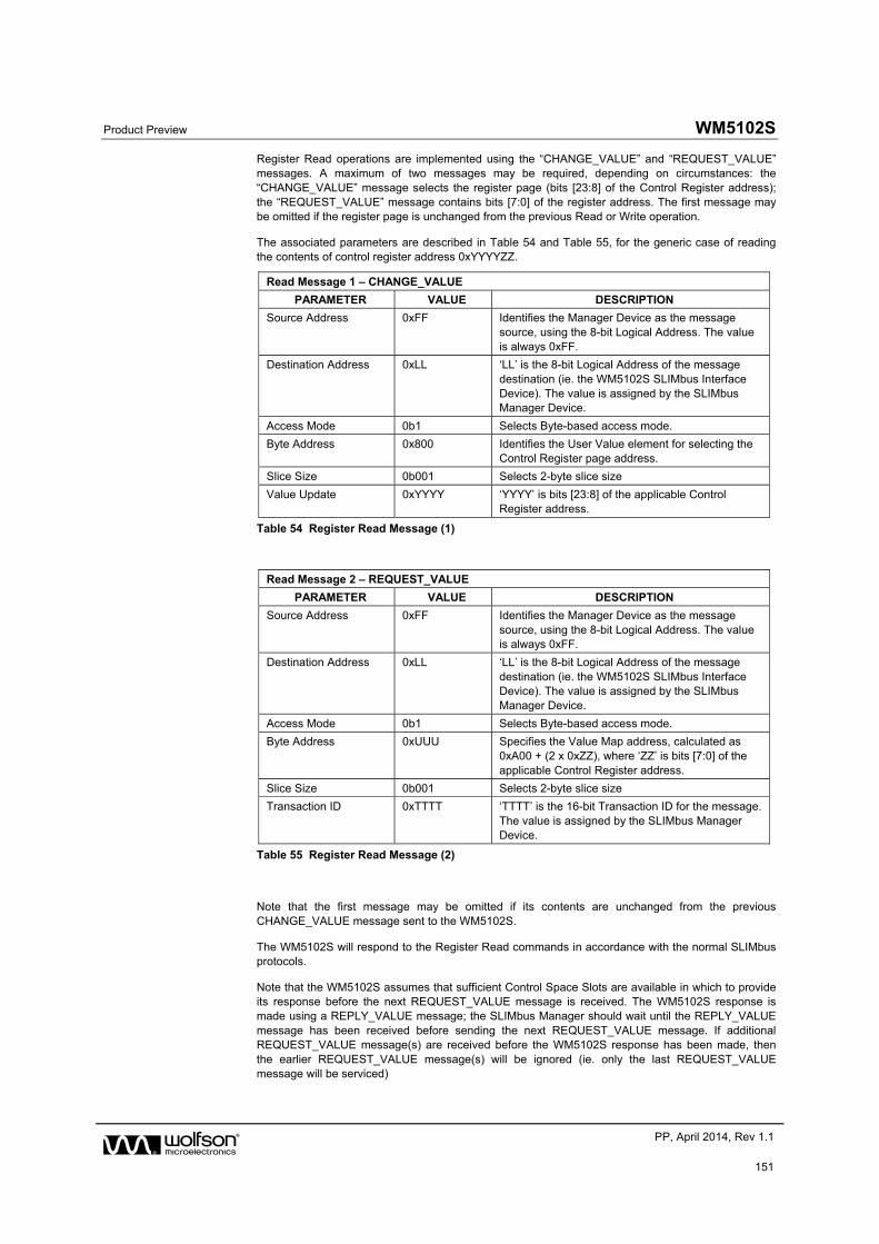
Product Preview WM5102S
w PP, April 2014, Rev 1.1
151
Register Read operations are implemented using the “CHANGE_VALUE” and “REQUEST_VALUE” messages. A maximum of two messages may be required, depending on circumstances: the “CHANGE_VALUE” message selects the register page (bits [23:8] of the Control Register address); the “REQUEST_VALUE” message contains bits [7:0] of the register address. The first message may be omitted if the register page is unchanged from the previous Read or Write operation.
The associated parameters are described in Table 54 and Table 55, for the generic case of reading the contents of control register address 0xYYYYZZ.
Read Message 1 – CHANGE_VALUE
PARAMETER VALUE DESCRIPTION
Source Address 0xFF Identifies the Manager Device as the message source, using the 8-bit Logical Address. The value is always 0xFF.
Destination Address 0xLL ‘LL’ is the 8-bit Logical Address of the message destination (ie. the WM5102S SLIMbus Interface Device). The value is assigned by the SLIMbus Manager Device.
Access Mode 0b1 Selects Byte-based access mode.
Byte Address 0x800 Identifies the User Value element for selecting the Control Register page address.
Slice Size 0b001 Selects 2-byte slice size
Value Update 0xYYYY ‘YYYY’ is bits [23:8] of the applicable Control Register address.
Table 54 Register Read Message (1)
Read Message 2 – REQUEST_VALUE
PARAMETER VALUE DESCRIPTION
Source Address 0xFF Identifies the Manager Device as the message source, using the 8-bit Logical Address. The value is always 0xFF.
Destination Address 0xLL ‘LL’ is the 8-bit Logical Address of the message destination (ie. the WM5102S SLIMbus Interface Device). The value is assigned by the SLIMbus Manager Device.
Access Mode 0b1 Selects Byte-based access mode.
Byte Address 0xUUU Specifies the Value Map address, calculated as 0xA00 + (2 x 0xZZ), where ‘ZZ’ is bits [7:0] of the applicable Control Register address.
Slice Size 0b001 Selects 2-byte slice size
Transaction ID 0xTTTT ‘TTTT’ is the 16-bit Transaction ID for the message. The value is assigned by the SLIMbus Manager Device.
Table 55 Register Read Message (2)
Note that the first message may be omitted if its contents are unchanged from the previous CHANGE_VALUE message sent to the WM5102S.
The WM5102S will respond to the Register Read commands in accordance with the normal SLIMbus protocols.
Note that the WM5102S assumes that sufficient Control Space Slots are available in which to provide its response before the next REQUEST_VALUE message is received. The WM5102S response is made using a REPLY_VALUE message; the SLIMbus Manager should wait until the REPLY_VALUE message has been received before sending the next REQUEST_VALUE message. If additional REQUEST_VALUE message(s) are received before the WM5102S response has been made, then the earlier REQUEST_VALUE message(s) will be ignored (ie. only the last REQUEST_VALUE message will be serviced)
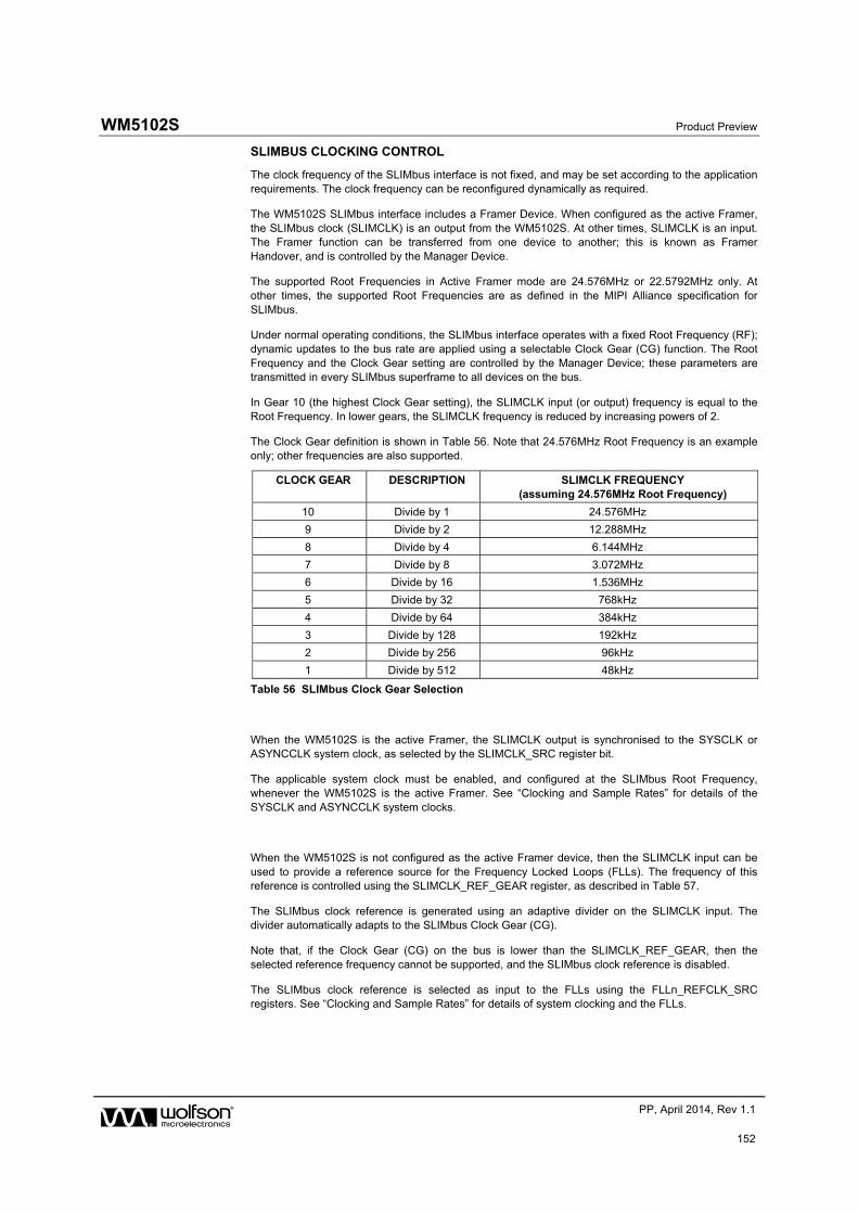
WM5102S Product Preview
w PP, April 2014, Rev 1.1
152
SLIMBUS CLOCKING CONTROL
The clock frequency of the SLIMbus interface is not fixed, and may be set according to the application requirements. The clock frequency can be reconfigured dynamically as required.
The WM5102S SLIMbus interface includes a Framer Device. When configured as the active Framer, the SLIMbus clock (SLIMCLK) is an output from the WM5102S. At other times, SLIMCLK is an input. The Framer function can be transferred from one device to another; this is known as Framer Handover, and is controlled by the Manager Device.
The supported Root Frequencies in Active Framer mode are 24.576MHz or 22.5792MHz only. At other times, the supported Root Frequencies are as defined in the MIPI Alliance specification for SLIMbus.
Under normal operating conditions, the SLIMbus interface operates with a fixed Root Frequency (RF); dynamic updates to the bus rate are applied using a selectable Clock Gear (CG) function. The Root Frequency and the Clock Gear setting are controlled by the Manager Device; these parameters are transmitted in every SLIMbus superframe to all devices on the bus.
In Gear 10 (the highest Clock Gear setting), the SLIMCLK input (or output) frequency is equal to the Root Frequency. In lower gears, the SLIMCLK frequency is reduced by increasing powers of 2.
The Clock Gear definition is shown in Table 56. Note that 24.576MHz Root Frequency is an example only; other frequencies are also supported.
CLOCK GEAR DESCRIPTION SLIMCLK FREQUENCY (assuming 24.576MHz Root Frequency)
10 Divide by 1 24.576MHz
9 Divide by 2 12.288MHz
8 Divide by 4 6.144MHz
7 Divide by 8 3.072MHz
6 Divide by 16 1.536MHz
5 Divide by 32 768kHz
4 Divide by 64 384kHz
3 Divide by 128 192kHz
2 Divide by 256 96kHz
1 Divide by 512 48kHz
Table 56 SLIMbus Clock Gear Selection
When the WM5102S is the active Framer, the SLIMCLK output is synchronised to the SYSCLK or ASYNCCLK system clock, as selected by the SLIMCLK_SRC register bit.
The applicable system clock must be enabled, and configured at the SLIMbus Root Frequency, whenever the WM5102S is the active Framer. See “Clocking and Sample Rates” for details of the SYSCLK and ASYNCCLK system clocks.
When the WM5102S is not configured as the active Framer device, then the SLIMCLK input can be used to provide a reference source for the Frequency Locked Loops (FLLs). The frequency of this reference is controlled using the SLIMCLK_REF_GEAR register, as described in Table 57.
The SLIMbus clock reference is generated using an adaptive divider on the SLIMCLK input. The divider automatically adapts to the SLIMbus Clock Gear (CG).
Note that, if the Clock Gear (CG) on the bus is lower than the SLIMCLK_REF_GEAR, then the selected reference frequency cannot be supported, and the SLIMbus clock reference is disabled.
The SLIMbus clock reference is selected as input to the FLLs using the FLLn_REFCLK_SRC registers. See “Clocking and Sample Rates” for details of system clocking and the FLLs.
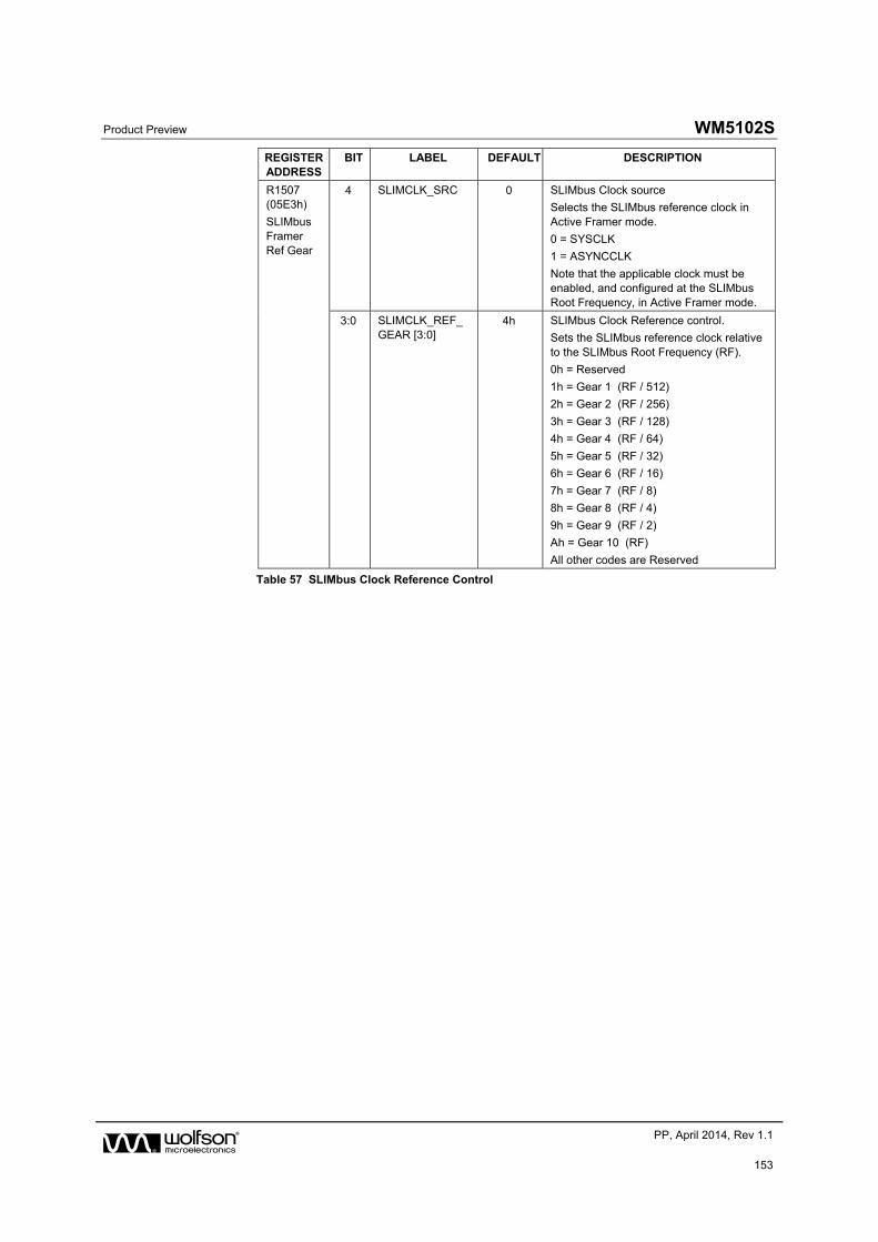
Product Preview WM5102S
w PP, April 2014, Rev 1.1
153
REGISTER ADDRESS
BIT LABEL DEFAULT DESCRIPTION
R1507 (05E3h)
SLIMbus Framer Ref Gear
4 SLIMCLK_SRC 0 SLIMbus Clock source
Selects the SLIMbus reference clock in Active Framer mode.
0 = SYSCLK
1 = ASYNCCLK
Note that the applicable clock must be enabled, and configured at the SLIMbus Root Frequency, in Active Framer mode.
3:0 SLIMCLK_REF_GEAR [3:0]
4h SLIMbus Clock Reference control.
Sets the SLIMbus reference clock relative to the SLIMbus Root Frequency (RF).
0h = Reserved
1h = Gear 1 (RF / 512)
2h = Gear 2 (RF / 256)
3h = Gear 3 (RF / 128)
4h = Gear 4 (RF / 64)
5h = Gear 5 (RF / 32)
6h = Gear 6 (RF / 16)
7h = Gear 7 (RF / 8)
8h = Gear 8 (RF / 4)
9h = Gear 9 (RF / 2)
Ah = Gear 10 (RF)
All other codes are Reserved
Table 57 SLIMbus Clock Reference Control
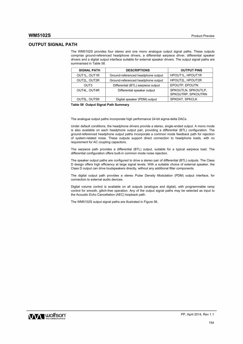
WM5102S Product Preview
w PP, April 2014, Rev 1.1
154
OUTPUT SIGNAL PATH
The WM5102S provides four stereo and one mono analogue output signal paths. These outputs comprise ground-referenced headphone drivers, a differential earpiece driver, differential speaker drivers and a digital output interface suitable for external speaker drivers. The output signal paths are summarised in Table 58.
SIGNAL PATH DESCRIPTIONS OUTPUT PINS
OUT1L, OUT1R Ground-referenced headphone output HPOUT1L, HPOUT1R
OUT2L, OUT2R Ground-referenced headphone output HPOUT2L, HPOUT2R
OUT3 Differential (BTL) earpiece output EPOUTP, EPOUTN
OUT4L, OUT4R Differential speaker output SPKOUTLN, SPKOUTLP, SPKOUTRP, SPKOUTRN
OUT5L, OUT5R Digital speaker (PDM) output SPKDAT, SPKCLK
Table 58 Output Signal Path Summary
The analogue output paths incorporate high performance 24-bit sigma-delta DACs.
Under default conditions, the headphone drivers provide a stereo, single-ended output. A mono mode is also available on each headphone output pair, providing a differential (BTL) configuration. The ground-referenced headphone output paths incorporate a common mode feedback path for rejection of system-related noise. These outputs support direct connection to headphone loads, with no requirement for AC coupling capacitors.
The earpiece path provides a differential (BTL) output, suitable for a typical earpiece load. The differential configuration offers built-in common mode noise rejection.
The speaker output paths are configured to drive a stereo pair of differential (BTL) outputs. The Class D design offers high efficiency at large signal levels. With a suitable choice of external speaker, the Class D output can drive loudspeakers directly, without any additional filter components.
The digital output path provides a stereo Pulse Density Modulation (PDM) output interface, for connection to external audio devices.
Digital volume control is available on all outputs (analogue and digital), with programmable ramp control for smooth, glitch-free operation. Any of the output signal paths may be selected as input to the Acoustic Echo Cancellation (AEC) loopback path.
The WM5102S output signal paths are illustrated in Figure 56.
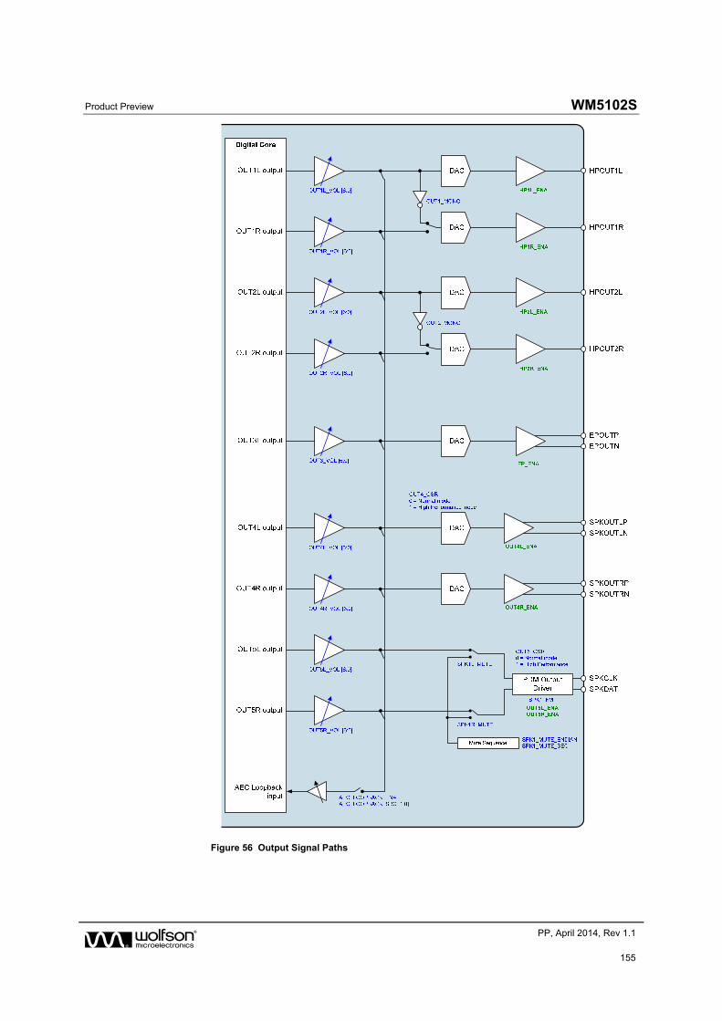
Product Preview WM5102S
w PP, April 2014, Rev 1.1
155
Figure 56 Output Signal Paths
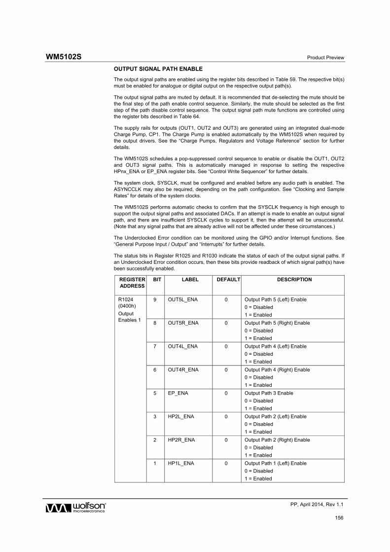
WM5102S Product Preview
w PP, April 2014, Rev 1.1
156
OUTPUT SIGNAL PATH ENABLE
The output signal paths are enabled using the register bits described in Table 59. The respective bit(s) must be enabled for analogue or digital output on the respective output path(s).
The output signal paths are muted by default. It is recommended that de-selecting the mute should be the final step of the path enable control sequence. Similarly, the mute should be selected as the first step of the path disable control sequence. The output signal path mute functions are controlled using the register bits described in Table 64.
The supply rails for outputs (OUT1, OUT2 and OUT3) are generated using an integrated dual-mode Charge Pump, CP1. The Charge Pump is enabled automatically by the WM5102S when required by the output drivers. See the “Charge Pumps, Regulators and Voltage Reference” section for further details.
The WM5102S schedules a pop-suppressed control sequence to enable or disable the OUT1, OUT2 and OUT3 signal paths. This is automatically managed in response to setting the respective HPnx_ENA or EP_ENA register bits. See “Control Write Sequencer” for further details.
The system clock, SYSCLK, must be configured and enabled before any audio path is enabled. The ASYNCCLK may also be required, depending on the path configuration. See “Clocking and Sample Rates” for details of the system clocks.
The WM5102S performs automatic checks to confirm that the SYSCLK frequency is high enough to support the output signal paths and associated DACs. If an attempt is made to enable an output signal path, and there are insufficient SYSCLK cycles to support it, then the attempt will be unsuccessful. (Note that any signal paths that are already active will not be affected under these circumstances.)
The Underclocked Error condition can be monitored using the GPIO and/or Interrupt functions. See “General Purpose Input / Output” and “Interrupts” for further details.
The status bits in Register R1025 and R1030 indicate the status of each of the output signal paths. If an Underclocked Error condition occurs, then these bits provide readback of which signal path(s) have been successfully enabled.
REGISTER ADDRESS
BIT LABEL DEFAULT DESCRIPTION
R1024 (0400h)
Output Enables 1
9 OUT5L_ENA 0 Output Path 5 (Left) Enable
0 = Disabled
1 = Enabled
8 OUT5R_ENA 0 Output Path 5 (Right) Enable
0 = Disabled
1 = Enabled
7 OUT4L_ENA 0 Output Path 4 (Left) Enable
0 = Disabled
1 = Enabled
6 OUT4R_ENA 0 Output Path 4 (Right) Enable
0 = Disabled
1 = Enabled
5 EP_ENA 0 Output Path 3 Enable
0 = Disabled
1 = Enabled
3 HP2L_ENA 0 Output Path 2 (Left) Enable
0 = Disabled
1 = Enabled
2 HP2R_ENA 0 Output Path 2 (Right) Enable
0 = Disabled
1 = Enabled
1 HP1L_ENA 0 Output Path 1 (Left) Enable
0 = Disabled
1 = Enabled
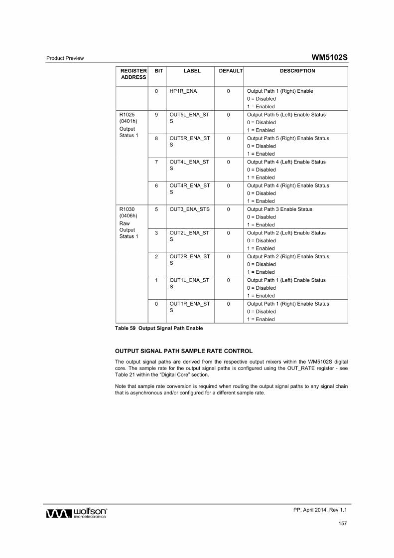
Product Preview WM5102S
w PP, April 2014, Rev 1.1
157
REGISTER ADDRESS
BIT LABEL DEFAULT DESCRIPTION
0 HP1R_ENA 0 Output Path 1 (Right) Enable
0 = Disabled
1 = Enabled
R1025 (0401h)
Output Status 1
9 OUT5L_ENA_STS
0 Output Path 5 (Left) Enable Status
0 = Disabled
1 = Enabled
8 OUT5R_ENA_STS
0 Output Path 5 (Right) Enable Status
0 = Disabled
1 = Enabled
7 OUT4L_ENA_STS
0 Output Path 4 (Left) Enable Status
0 = Disabled
1 = Enabled
6 OUT4R_ENA_STS
0 Output Path 4 (Right) Enable Status
0 = Disabled
1 = Enabled
R1030 (0406h)
Raw Output Status 1
5 OUT3_ENA_STS 0 Output Path 3 Enable Status
0 = Disabled
1 = Enabled
3 OUT2L_ENA_STS
0 Output Path 2 (Left) Enable Status
0 = Disabled
1 = Enabled
2 OUT2R_ENA_STS
0 Output Path 2 (Right) Enable Status
0 = Disabled
1 = Enabled
1 OUT1L_ENA_STS
0 Output Path 1 (Left) Enable Status
0 = Disabled
1 = Enabled
0 OUT1R_ENA_STS
0 Output Path 1 (Right) Enable Status
0 = Disabled
1 = Enabled
Table 59 Output Signal Path Enable
OUTPUT SIGNAL PATH SAMPLE RATE CONTROL
The output signal paths are derived from the respective output mixers within the WM5102S digital core. The sample rate for the output signal paths is configured using the OUT_RATE register - see Table 21 within the “Digital Core” section.
Note that sample rate conversion is required when routing the output signal paths to any signal chain that is asynchronous and/or configured for a different sample rate.
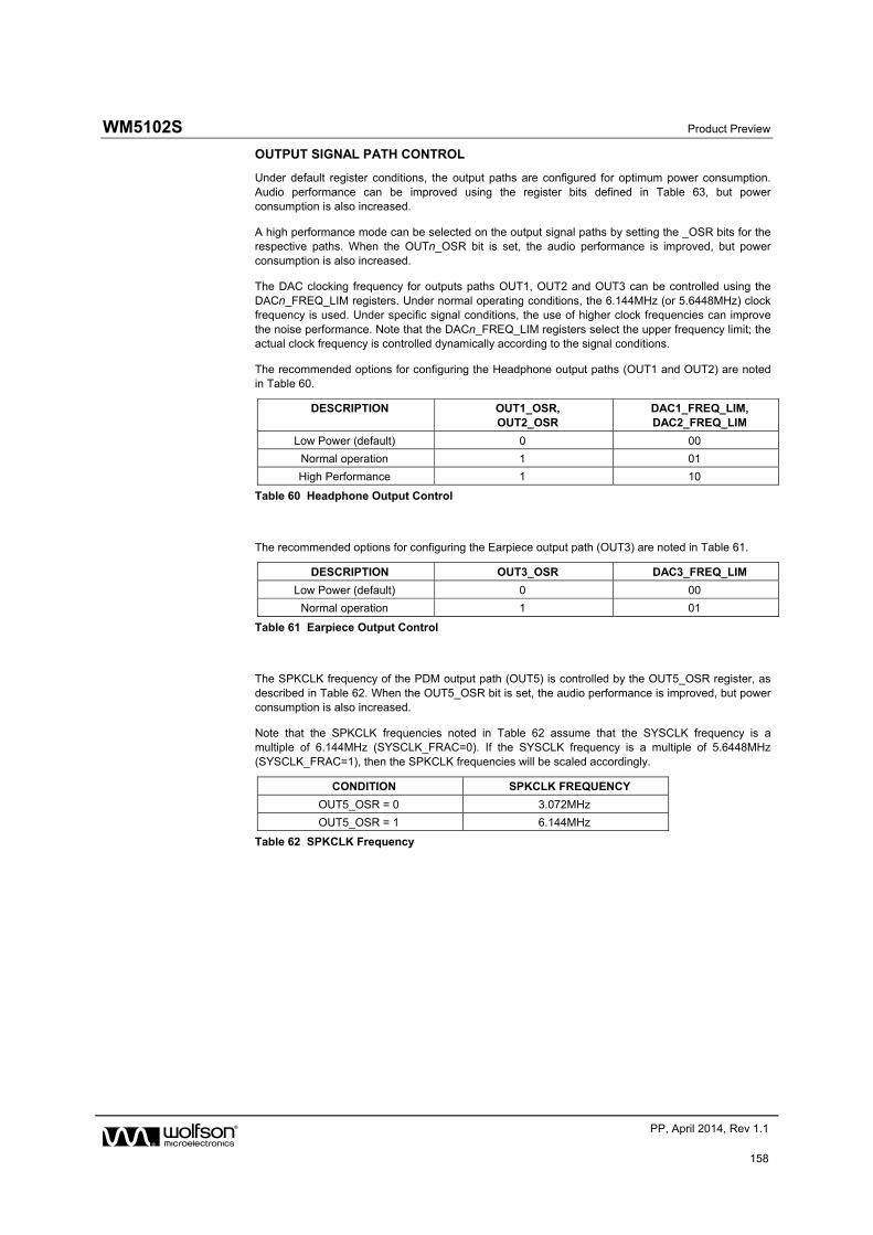
WM5102S Product Preview
w PP, April 2014, Rev 1.1
158
OUTPUT SIGNAL PATH CONTROL
Under default register conditions, the output paths are configured for optimum power consumption. Audio performance can be improved using the register bits defined in Table 63, but power consumption is also increased.
A high performance mode can be selected on the output signal paths by setting the _OSR bits for the respective paths. When the OUTn_OSR bit is set, the audio performance is improved, but power consumption is also increased.
The DAC clocking frequency for outputs paths OUT1, OUT2 and OUT3 can be controlled using the DACn_FREQ_LIM registers. Under normal operating conditions, the 6.144MHz (or 5.6448MHz) clock frequency is used. Under specific signal conditions, the use of higher clock frequencies can improve the noise performance. Note that the DACn_FREQ_LIM registers select the upper frequency limit; the actual clock frequency is controlled dynamically according to the signal conditions.
The recommended options for configuring the Headphone output paths (OUT1 and OUT2) are noted in Table 60.
DESCRIPTION OUT1_OSR, OUT2_OSR
DAC1_FREQ_LIM, DAC2_FREQ_LIM
Low Power (default) 0 00
Normal operation 1 01
High Performance 1 10
Table 60 Headphone Output Control
The recommended options for configuring the Earpiece output path (OUT3) are noted in Table 61.
DESCRIPTION OUT3_OSR DAC3_FREQ_LIM
Low Power (default) 0 00
Normal operation 1 01
Table 61 Earpiece Output Control
The SPKCLK frequency of the PDM output path (OUT5) is controlled by the OUT5_OSR register, as described in Table 62. When the OUT5_OSR bit is set, the audio performance is improved, but power consumption is also increased.
Note that the SPKCLK frequencies noted in Table 62 assume that the SYSCLK frequency is a multiple of 6.144MHz (SYSCLK_FRAC=0). If the SYSCLK frequency is a multiple of 5.6448MHz (SYSCLK_FRAC=1), then the SPKCLK frequencies will be scaled accordingly.
CONDITION SPKCLK FREQUENCY
OUT5_OSR = 0 3.072MHz
OUT5_OSR = 1 6.144MHz
Table 62 SPKCLK Frequency

Product Preview WM5102S
w PP, April 2014, Rev 1.1
159
REGISTER ADDRESS
BIT LABEL DEFAULT DESCRIPTION
R1040 (0410h)
Output Path Config 1L
15:14 DAC1_FREQ_RANGE_LIM [1:0]
00 Output Path 1 Clocking Frequency Limit
When OUT1_OSR=0
00 = 3.072MHz (2.8224MHz)
01 = 6.144MHz (5.6448MHz)
10 = 12.288MHz (11.2896MHz)
11 = Reserved
When OUT1_OSR=1
00 = 6.144MHz (5.6448MHz)
01 = 6.144MHz (5.6448MHz)
10 = 12.288MHz (11.2896MHz)
11 = Reserved
Note that the Clocking Frequency will be <= SYSCLK under all register settings. The frequencies in brackets apply for 44.1kHz-related sample rates only (ie. SAMPLE_RATE_n = 01XXX).
13 OUT1_OSR 0 Output Path 1 Oversample Rate
0 = Normal mode
1 = High Performance mode
R1048 (0418h)
Output Path Config 2L
15:14 DAC2_FREQ_RANGE_LIM [1:0]
00 Output Path 2 Clocking Frequency Limit
When OUT2_OSR=0
00 = 3.072MHz (2.8224MHz)
01 = 6.144MHz (5.6448MHz)
10 = 12.288MHz (11.2896MHz)
11 = Reserved
When OUT2_OSR=1
00 = 6.144MHz (5.6448MHz)
01 = 6.144MHz (5.6448MHz)
10 = 12.288MHz (11.2896MHz)
11 = Reserved
Note that the Clocking Frequency will be <= SYSCLK under all register settings. The frequencies in brackets apply for 44.1kHz-related sample rates only (ie. SAMPLE_RATE_n = 01XXX).
13 OUT2_OSR 0 Output Path 2 Oversample Rate
0 = Normal mode
1 = High Performance mode
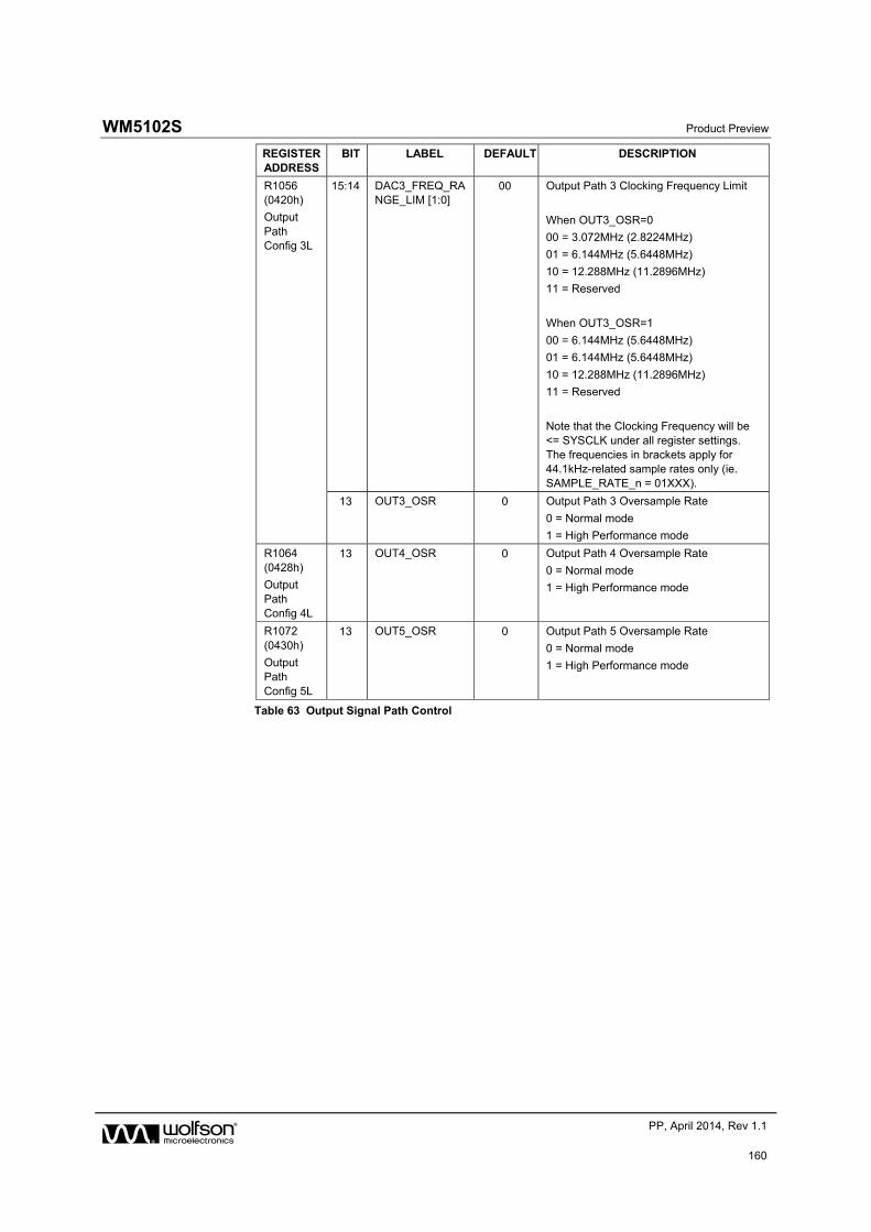
WM5102S Product Preview
w PP, April 2014, Rev 1.1
160
REGISTER ADDRESS
BIT LABEL DEFAULT DESCRIPTION
R1056 (0420h)
Output Path Config 3L
15:14 DAC3_FREQ_RANGE_LIM [1:0]
00 Output Path 3 Clocking Frequency Limit
When OUT3_OSR=0
00 = 3.072MHz (2.8224MHz)
01 = 6.144MHz (5.6448MHz)
10 = 12.288MHz (11.2896MHz)
11 = Reserved
When OUT3_OSR=1
00 = 6.144MHz (5.6448MHz)
01 = 6.144MHz (5.6448MHz)
10 = 12.288MHz (11.2896MHz)
11 = Reserved
Note that the Clocking Frequency will be <= SYSCLK under all register settings. The frequencies in brackets apply for 44.1kHz-related sample rates only (ie. SAMPLE_RATE_n = 01XXX).
13 OUT3_OSR 0 Output Path 3 Oversample Rate
0 = Normal mode
1 = High Performance mode
R1064 (0428h)
Output Path Config 4L
13 OUT4_OSR 0 Output Path 4 Oversample Rate
0 = Normal mode
1 = High Performance mode
R1072 (0430h)
Output Path Config 5L
13 OUT5_OSR 0 Output Path 5 Oversample Rate
0 = Normal mode
1 = High Performance mode
Table 63 Output Signal Path Control

Product Preview WM5102S
w PP, April 2014, Rev 1.1
161
OUTPUT SIGNAL PATH DIGITAL VOLUME CONTROL
A digital volume control is provided on each of the output signal paths, providing -64dB to +31.5dB gain control in 0.5dB steps. An independent mute control is also provided for each output signal path.
Whenever the gain or mute setting is changed, the signal path gain is ramped up or down to the new settings at a programmable rate. For increasing gain (or un-mute), the rate is controlled by the OUT_VI_RAMP register. For decreasing gain (or mute), the rate is controlled by the OUT_VD_RAMP register. Note that the OUT_VI_RAMP and OUT_VD_RAMP registers should not be changed while a volume ramp is in progress.
The OUT_VU bits control the loading of the output signal path digital volume and mute controls. When OUT_VU is set to 0, the digital volume and mute settings will be loaded into the respective control register, but will not actually change the signal path gain. The digital volume and mute settings on all of the output signal paths are updated when a 1 is written to OUT_VU. This makes it possible to update the gain of multiple signal paths simultaneously.
For correct gain ramp behaviour, the OUT_VU bits should not be written during the 0.28ms after any of the output path enable bits (see Table 59) have been asserted. It is recommended that the output path mute bit be set when the respective output driver is enabled; the signal path can then be un-muted after the 0.28ms has elapsed.
Note that, although the digital volume control registers provide 0.5dB steps, the internal circuits provide signal gain adjustment in 0.125dB steps. This allows a very high degree of gain control, and smooth volume ramping under all operating conditions.
The digital volume control register fields are described in Table 64 and Table 65.
REGISTER ADDRESS
BIT LABEL DEFAULT DESCRIPTION
R1033 (0409h)
Output Volume Ramp
6:4 OUT_VD_RAMP [2:0]
010 Output Volume Decreasing Ramp Rate
(seconds/6dB)
000 = 0ms
001 = 0.5ms
010 = 1ms
011 = 2ms
100 = 4ms
101 = 8ms
110 = 15ms
111 = 30ms
This register should not be changed while a volume ramp is in progress.
2:0 OUT_VI_RAMP [2:0]
010 Output Volume Increasing Ramp Rate
(seconds/6dB)
000 = 0ms
001 = 0.5ms
010 = 1ms
011 = 2ms
100 = 4ms
101 = 8ms
110 = 15ms
111 = 30ms
This register should not be changed while a volume ramp is in progress.
R1041 (0411h)
DAC Digital Volume 1L
9 OUT_VU Output Signal Paths Volume Update
Writing a 1 to this bit will cause the Output Signal Paths Volume and Mute settings to be updated simultaneously
8 OUT1L_MUTE 1 Output Path 1 (Left) Digital Mute
0 = Un-mute
1 = Mute
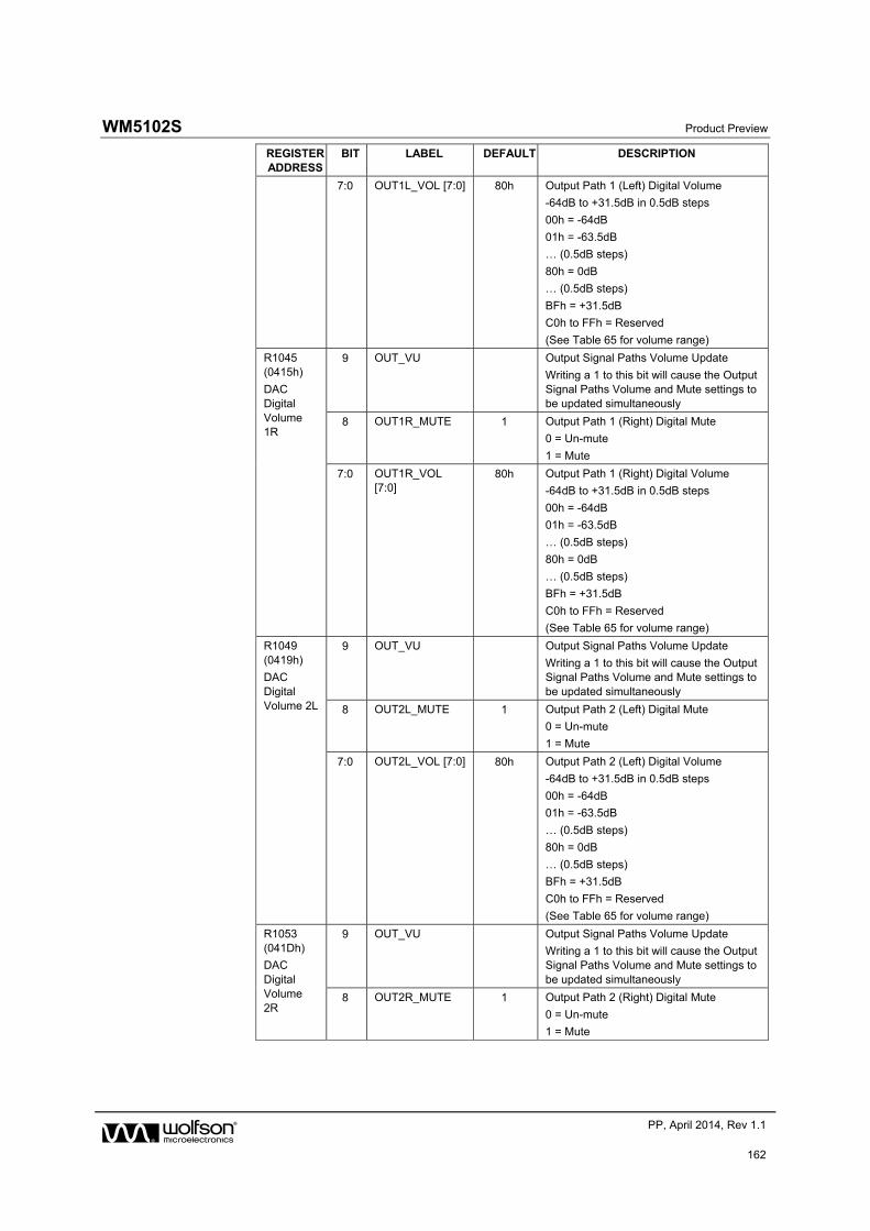
WM5102S Product Preview
w PP, April 2014, Rev 1.1
162
REGISTER ADDRESS
BIT LABEL DEFAULT DESCRIPTION
7:0 OUT1L_VOL [7:0] 80h Output Path 1 (Left) Digital Volume
-64dB to +31.5dB in 0.5dB steps
00h = -64dB
01h = -63.5dB
… (0.5dB steps)
80h = 0dB
… (0.5dB steps)
BFh = +31.5dB
C0h to FFh = Reserved
(See Table 65 for volume range)
R1045 (0415h)
DAC Digital Volume 1R
9 OUT_VU Output Signal Paths Volume Update
Writing a 1 to this bit will cause the Output Signal Paths Volume and Mute settings to be updated simultaneously
8 OUT1R_MUTE 1 Output Path 1 (Right) Digital Mute
0 = Un-mute
1 = Mute
7:0 OUT1R_VOL [7:0]
80h Output Path 1 (Right) Digital Volume
-64dB to +31.5dB in 0.5dB steps
00h = -64dB
01h = -63.5dB
… (0.5dB steps)
80h = 0dB
… (0.5dB steps)
BFh = +31.5dB
C0h to FFh = Reserved
(See Table 65 for volume range)
R1049 (0419h)
DAC Digital Volume 2L
9 OUT_VU Output Signal Paths Volume Update
Writing a 1 to this bit will cause the Output Signal Paths Volume and Mute settings to be updated simultaneously
8 OUT2L_MUTE 1 Output Path 2 (Left) Digital Mute
0 = Un-mute
1 = Mute
7:0 OUT2L_VOL [7:0] 80h Output Path 2 (Left) Digital Volume
-64dB to +31.5dB in 0.5dB steps
00h = -64dB
01h = -63.5dB
… (0.5dB steps)
80h = 0dB
… (0.5dB steps)
BFh = +31.5dB
C0h to FFh = Reserved
(See Table 65 for volume range)
R1053 (041Dh)
DAC Digital Volume 2R
9 OUT_VU Output Signal Paths Volume Update
Writing a 1 to this bit will cause the Output Signal Paths Volume and Mute settings to be updated simultaneously
8 OUT2R_MUTE 1 Output Path 2 (Right) Digital Mute
0 = Un-mute
1 = Mute
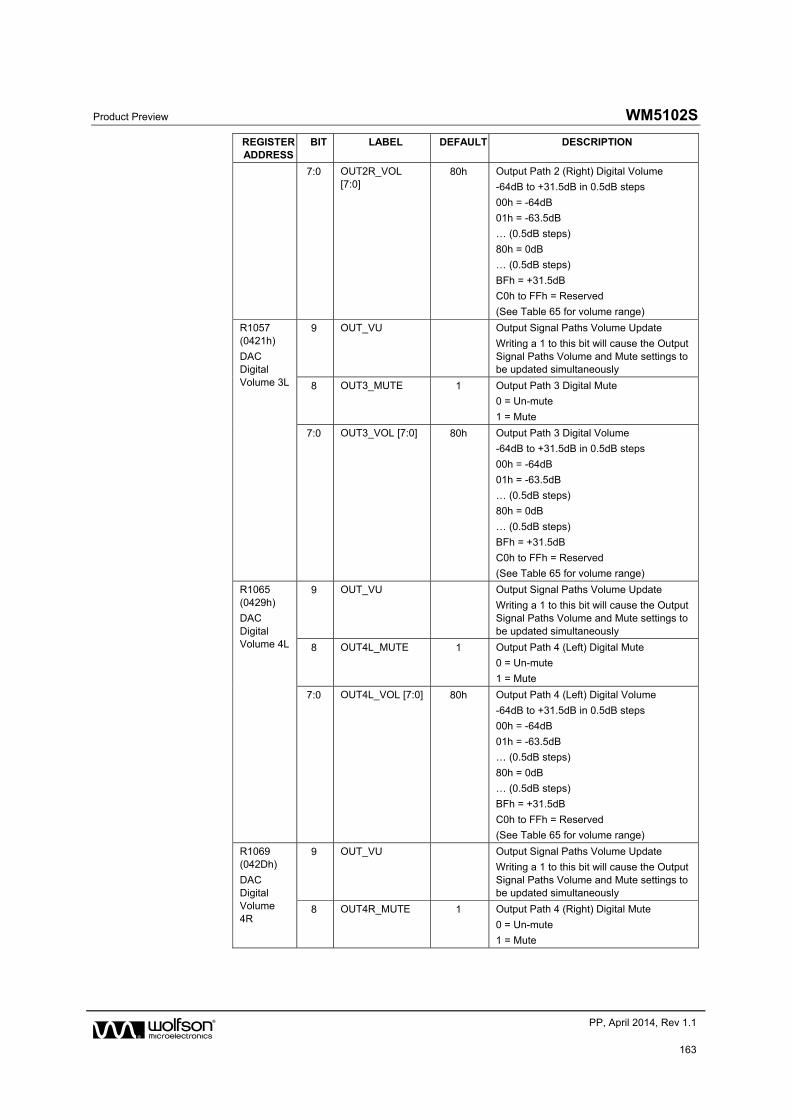
Product Preview WM5102S
w PP, April 2014, Rev 1.1
163
REGISTER ADDRESS
BIT LABEL DEFAULT DESCRIPTION
7:0 OUT2R_VOL [7:0]
80h Output Path 2 (Right) Digital Volume
-64dB to +31.5dB in 0.5dB steps
00h = -64dB
01h = -63.5dB
… (0.5dB steps)
80h = 0dB
… (0.5dB steps)
BFh = +31.5dB
C0h to FFh = Reserved
(See Table 65 for volume range)
R1057 (0421h)
DAC Digital Volume 3L
9 OUT_VU Output Signal Paths Volume Update
Writing a 1 to this bit will cause the Output Signal Paths Volume and Mute settings to be updated simultaneously
8 OUT3_MUTE 1 Output Path 3 Digital Mute
0 = Un-mute
1 = Mute
7:0 OUT3_VOL [7:0] 80h Output Path 3 Digital Volume
-64dB to +31.5dB in 0.5dB steps
00h = -64dB
01h = -63.5dB
… (0.5dB steps)
80h = 0dB
… (0.5dB steps)
BFh = +31.5dB
C0h to FFh = Reserved
(See Table 65 for volume range)
R1065 (0429h)
DAC Digital Volume 4L
9 OUT_VU Output Signal Paths Volume Update
Writing a 1 to this bit will cause the Output Signal Paths Volume and Mute settings to be updated simultaneously
8 OUT4L_MUTE 1 Output Path 4 (Left) Digital Mute
0 = Un-mute
1 = Mute
7:0 OUT4L_VOL [7:0] 80h Output Path 4 (Left) Digital Volume
-64dB to +31.5dB in 0.5dB steps
00h = -64dB
01h = -63.5dB
… (0.5dB steps)
80h = 0dB
… (0.5dB steps)
BFh = +31.5dB
C0h to FFh = Reserved
(See Table 65 for volume range)
R1069 (042Dh)
DAC Digital Volume 4R
9 OUT_VU Output Signal Paths Volume Update
Writing a 1 to this bit will cause the Output Signal Paths Volume and Mute settings to be updated simultaneously
8 OUT4R_MUTE 1 Output Path 4 (Right) Digital Mute
0 = Un-mute
1 = Mute
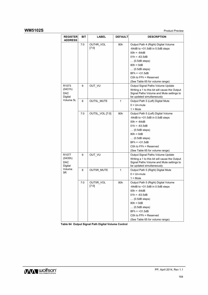
WM5102S Product Preview
w PP, April 2014, Rev 1.1
164
REGISTER ADDRESS
BIT LABEL DEFAULT DESCRIPTION
7:0 OUT4R_VOL [7:0]
80h Output Path 4 (Right) Digital Volume
-64dB to +31.5dB in 0.5dB steps
00h = -64dB
01h = -63.5dB
… (0.5dB steps)
80h = 0dB
… (0.5dB steps)
BFh = +31.5dB
C0h to FFh = Reserved
(See Table 65 for volume range)
R1073 (0431h)
DAC Digital Volume 5L
9 OUT_VU Output Signal Paths Volume Update
Writing a 1 to this bit will cause the Output Signal Paths Volume and Mute settings to be updated simultaneously
8 OUT5L_MUTE 1 Output Path 5 (Left) Digital Mute
0 = Un-mute
1 = Mute
7:0 OUT5L_VOL [7:0] 80h Output Path 5 (Left) Digital Volume
-64dB to +31.5dB in 0.5dB steps
00h = -64dB
01h = -63.5dB
… (0.5dB steps)
80h = 0dB
… (0.5dB steps)
BFh = +31.5dB
C0h to FFh = Reserved
(See Table 65 for volume range)
R1077 (0435h)
DAC Digital Volume 5R
9 OUT_VU Output Signal Paths Volume Update
Writing a 1 to this bit will cause the Output Signal Paths Volume and Mute settings to be updated simultaneously
8 OUT5R_MUTE 1 Output Path 5 (Right) Digital Mute
0 = Un-mute
1 = Mute
7:0 OUT5R_VOL [7:0]
80h Output Path 5 (Right) Digital Volume
-64dB to +31.5dB in 0.5dB steps
00h = -64dB
01h = -63.5dB
… (0.5dB steps)
80h = 0dB
… (0.5dB steps)
BFh = +31.5dB
C0h to FFh = Reserved
(See Table 65 for volume range)
Table 64 Output Signal Path Digital Volume Control
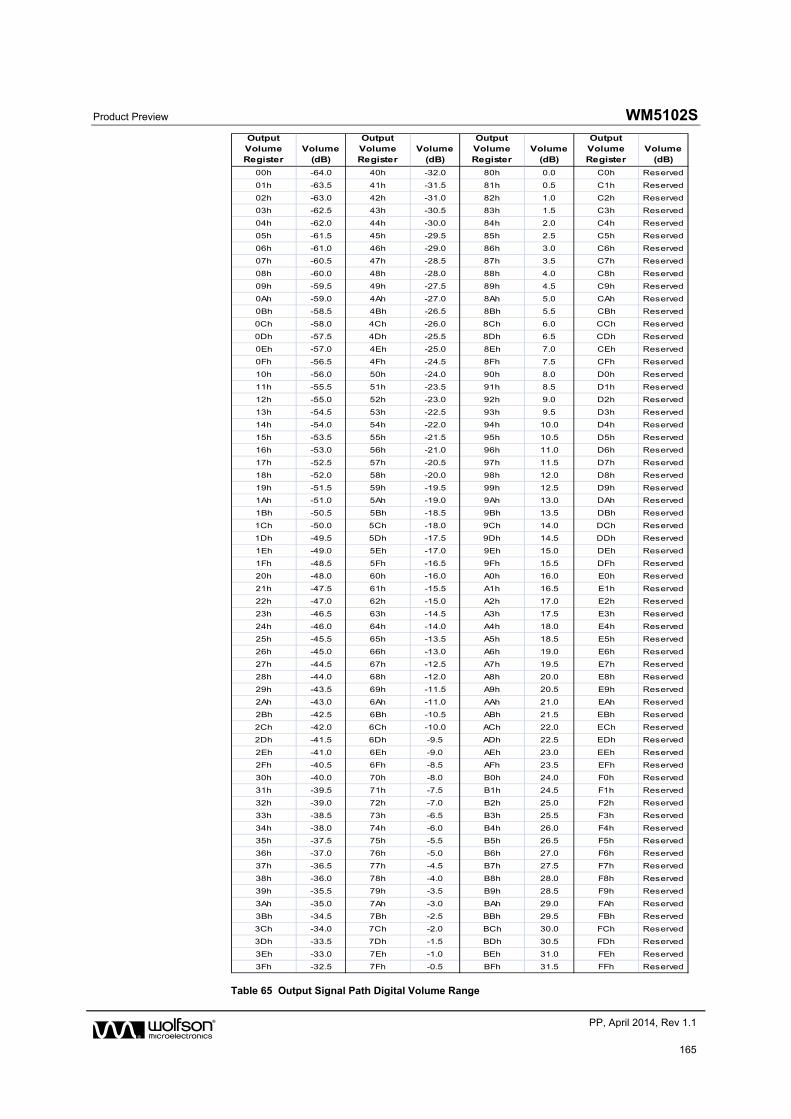
Product Preview WM5102S
w PP, April 2014, Rev 1.1
165
Output Volume Register
Volume (dB)
Output Volume Register
Volume (dB)
Output Volume Register
Volume (dB)
Output Volume Register
Volume (dB)
00h -64.0 40h -32.0 80h 0.0 C0h Reserved
01h -63.5 41h -31.5 81h 0.5 C1h Reserved
02h -63.0 42h -31.0 82h 1.0 C2h Reserved
03h -62.5 43h -30.5 83h 1.5 C3h Reserved
04h -62.0 44h -30.0 84h 2.0 C4h Reserved
05h -61.5 45h -29.5 85h 2.5 C5h Reserved
06h -61.0 46h -29.0 86h 3.0 C6h Reserved
07h -60.5 47h -28.5 87h 3.5 C7h Reserved
08h -60.0 48h -28.0 88h 4.0 C8h Reserved
09h -59.5 49h -27.5 89h 4.5 C9h Reserved
0Ah -59.0 4Ah -27.0 8Ah 5.0 CAh Reserved
0Bh -58.5 4Bh -26.5 8Bh 5.5 CBh Reserved
0Ch -58.0 4Ch -26.0 8Ch 6.0 CCh Reserved
0Dh -57.5 4Dh -25.5 8Dh 6.5 CDh Reserved
0Eh -57.0 4Eh -25.0 8Eh 7.0 CEh Reserved
0Fh -56.5 4Fh -24.5 8Fh 7.5 CFh Reserved
10h -56.0 50h -24.0 90h 8.0 D0h Reserved
11h -55.5 51h -23.5 91h 8.5 D1h Reserved
12h -55.0 52h -23.0 92h 9.0 D2h Reserved
13h -54.5 53h -22.5 93h 9.5 D3h Reserved
14h -54.0 54h -22.0 94h 10.0 D4h Reserved
15h -53.5 55h -21.5 95h 10.5 D5h Reserved
16h -53.0 56h -21.0 96h 11.0 D6h Reserved
17h -52.5 57h -20.5 97h 11.5 D7h Reserved
18h -52.0 58h -20.0 98h 12.0 D8h Reserved
19h -51.5 59h -19.5 99h 12.5 D9h Reserved
1Ah -51.0 5Ah -19.0 9Ah 13.0 DAh Reserved
1Bh -50.5 5Bh -18.5 9Bh 13.5 DBh Reserved
1Ch -50.0 5Ch -18.0 9Ch 14.0 DCh Reserved
1Dh -49.5 5Dh -17.5 9Dh 14.5 DDh Reserved
1Eh -49.0 5Eh -17.0 9Eh 15.0 DEh Reserved
1Fh -48.5 5Fh -16.5 9Fh 15.5 DFh Reserved
20h -48.0 60h -16.0 A0h 16.0 E0h Reserved
21h -47.5 61h -15.5 A1h 16.5 E1h Reserved
22h -47.0 62h -15.0 A2h 17.0 E2h Reserved
23h -46.5 63h -14.5 A3h 17.5 E3h Reserved
24h -46.0 64h -14.0 A4h 18.0 E4h Reserved
25h -45.5 65h -13.5 A5h 18.5 E5h Reserved
26h -45.0 66h -13.0 A6h 19.0 E6h Reserved
27h -44.5 67h -12.5 A7h 19.5 E7h Reserved
28h -44.0 68h -12.0 A8h 20.0 E8h Reserved
29h -43.5 69h -11.5 A9h 20.5 E9h Reserved
2Ah -43.0 6Ah -11.0 AAh 21.0 EAh Reserved
2Bh -42.5 6Bh -10.5 ABh 21.5 EBh Reserved
2Ch -42.0 6Ch -10.0 ACh 22.0 ECh Reserved
2Dh -41.5 6Dh -9.5 ADh 22.5 EDh Reserved
2Eh -41.0 6Eh -9.0 AEh 23.0 EEh Reserved
2Fh -40.5 6Fh -8.5 AFh 23.5 EFh Reserved
30h -40.0 70h -8.0 B0h 24.0 F0h Reserved
31h -39.5 71h -7.5 B1h 24.5 F1h Reserved
32h -39.0 72h -7.0 B2h 25.0 F2h Reserved
33h -38.5 73h -6.5 B3h 25.5 F3h Reserved
34h -38.0 74h -6.0 B4h 26.0 F4h Reserved
35h -37.5 75h -5.5 B5h 26.5 F5h Reserved
36h -37.0 76h -5.0 B6h 27.0 F6h Reserved
37h -36.5 77h -4.5 B7h 27.5 F7h Reserved
38h -36.0 78h -4.0 B8h 28.0 F8h Reserved
39h -35.5 79h -3.5 B9h 28.5 F9h Reserved
3Ah -35.0 7Ah -3.0 BAh 29.0 FAh Reserved
3Bh -34.5 7Bh -2.5 BBh 29.5 FBh Reserved
3Ch -34.0 7Ch -2.0 BCh 30.0 FCh Reserved
3Dh -33.5 7Dh -1.5 BDh 30.5 FDh Reserved
3Eh -33.0 7Eh -1.0 BEh 31.0 FEh Reserved
3Fh -32.5 7Fh -0.5 BFh 31.5 FFh Reserved
Table 65 Output Signal Path Digital Volume Range
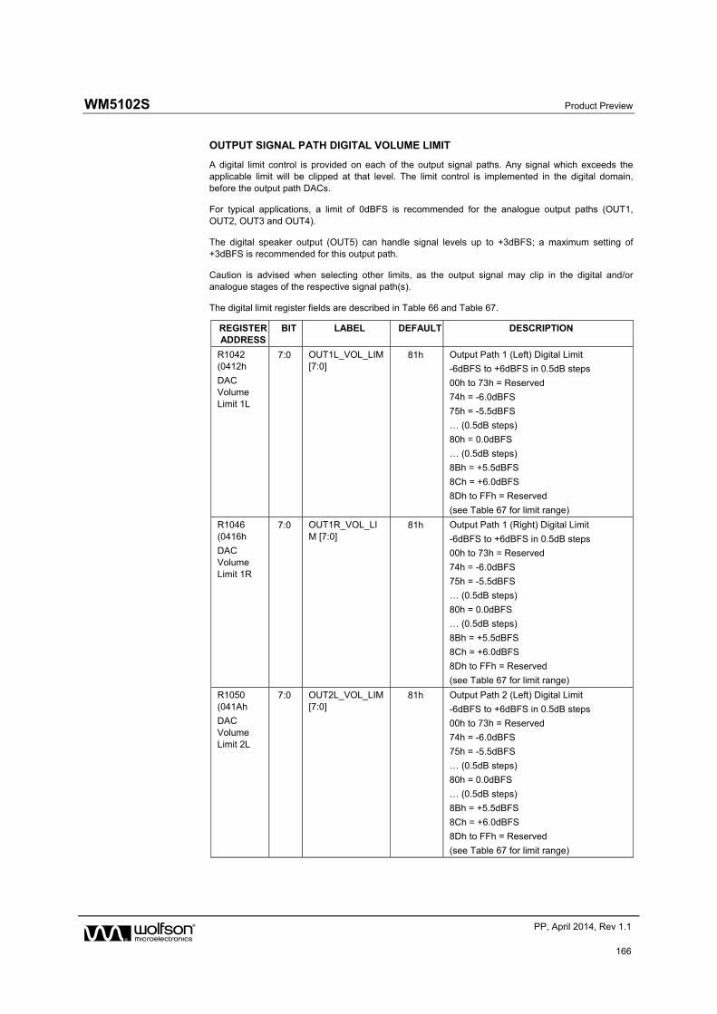
WM5102S Product Preview
w PP, April 2014, Rev 1.1
166
OUTPUT SIGNAL PATH DIGITAL VOLUME LIMIT
A digital limit control is provided on each of the output signal paths. Any signal which exceeds the applicable limit will be clipped at that level. The limit control is implemented in the digital domain, before the output path DACs.
For typical applications, a limit of 0dBFS is recommended for the analogue output paths (OUT1, OUT2, OUT3 and OUT4).
The digital speaker output (OUT5) can handle signal levels up to +3dBFS; a maximum setting of +3dBFS is recommended for this output path.
Caution is advised when selecting other limits, as the output signal may clip in the digital and/or analogue stages of the respective signal path(s).
The digital limit register fields are described in Table 66 and Table 67.
REGISTER ADDRESS
BIT LABEL DEFAULT DESCRIPTION
R1042 (0412h
DAC Volume Limit 1L
7:0 OUT1L_VOL_LIM [7:0]
81h Output Path 1 (Left) Digital Limit
-6dBFS to +6dBFS in 0.5dB steps
00h to 73h = Reserved
74h = -6.0dBFS
75h = -5.5dBFS
… (0.5dB steps)
80h = 0.0dBFS
… (0.5dB steps)
8Bh = +5.5dBFS
8Ch = +6.0dBFS
8Dh to FFh = Reserved
(see Table 67 for limit range)
R1046 (0416h
DAC Volume Limit 1R
7:0 OUT1R_VOL_LIM [7:0]
81h Output Path 1 (Right) Digital Limit
-6dBFS to +6dBFS in 0.5dB steps
00h to 73h = Reserved
74h = -6.0dBFS
75h = -5.5dBFS
… (0.5dB steps)
80h = 0.0dBFS
… (0.5dB steps)
8Bh = +5.5dBFS
8Ch = +6.0dBFS
8Dh to FFh = Reserved
(see Table 67 for limit range)
R1050 (041Ah
DAC Volume Limit 2L
7:0 OUT2L_VOL_LIM [7:0]
81h Output Path 2 (Left) Digital Limit
-6dBFS to +6dBFS in 0.5dB steps
00h to 73h = Reserved
74h = -6.0dBFS
75h = -5.5dBFS
… (0.5dB steps)
80h = 0.0dBFS
… (0.5dB steps)
8Bh = +5.5dBFS
8Ch = +6.0dBFS
8Dh to FFh = Reserved
(see Table 67 for limit range)
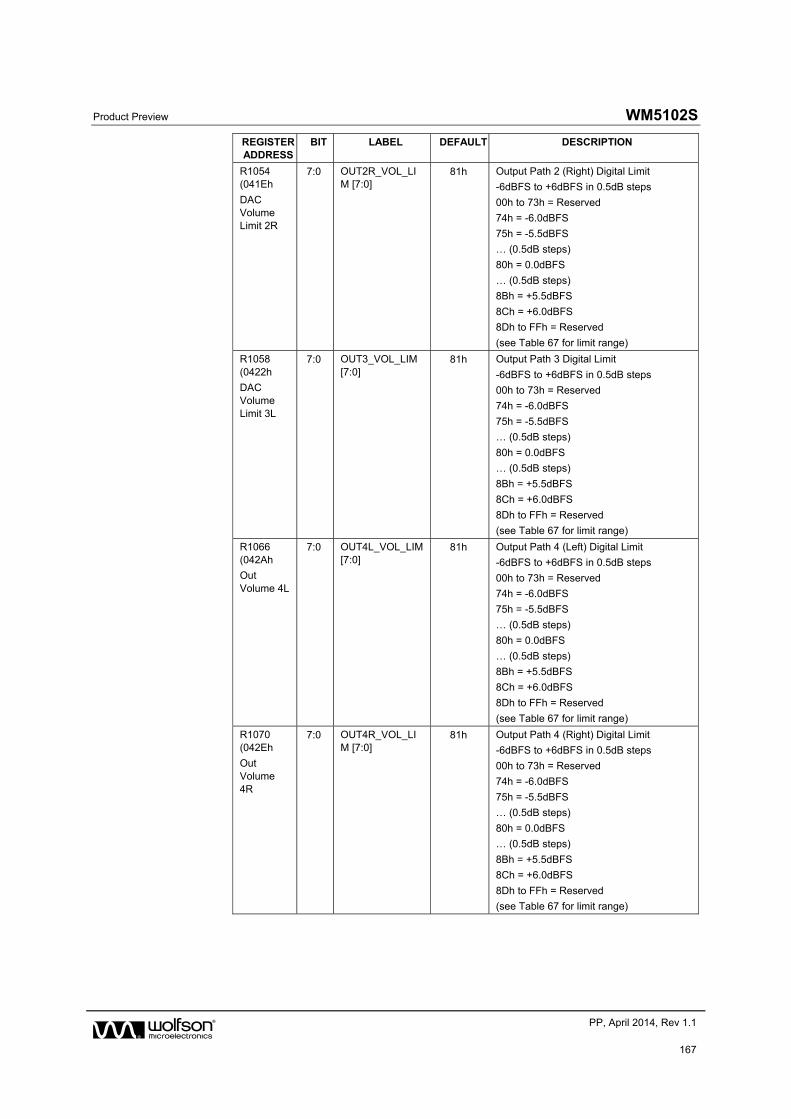
Product Preview WM5102S
w PP, April 2014, Rev 1.1
167
REGISTER ADDRESS
BIT LABEL DEFAULT DESCRIPTION
R1054 (041Eh
DAC Volume Limit 2R
7:0 OUT2R_VOL_LIM [7:0]
81h Output Path 2 (Right) Digital Limit
-6dBFS to +6dBFS in 0.5dB steps
00h to 73h = Reserved
74h = -6.0dBFS
75h = -5.5dBFS
… (0.5dB steps)
80h = 0.0dBFS
… (0.5dB steps)
8Bh = +5.5dBFS
8Ch = +6.0dBFS
8Dh to FFh = Reserved
(see Table 67 for limit range)
R1058 (0422h
DAC Volume Limit 3L
7:0 OUT3_VOL_LIM [7:0]
81h Output Path 3 Digital Limit
-6dBFS to +6dBFS in 0.5dB steps
00h to 73h = Reserved
74h = -6.0dBFS
75h = -5.5dBFS
… (0.5dB steps)
80h = 0.0dBFS
… (0.5dB steps)
8Bh = +5.5dBFS
8Ch = +6.0dBFS
8Dh to FFh = Reserved
(see Table 67 for limit range)
R1066 (042Ah
Out Volume 4L
7:0 OUT4L_VOL_LIM [7:0]
81h Output Path 4 (Left) Digital Limit
-6dBFS to +6dBFS in 0.5dB steps
00h to 73h = Reserved
74h = -6.0dBFS
75h = -5.5dBFS
… (0.5dB steps)
80h = 0.0dBFS
… (0.5dB steps)
8Bh = +5.5dBFS
8Ch = +6.0dBFS
8Dh to FFh = Reserved
(see Table 67 for limit range)
R1070 (042Eh
Out Volume 4R
7:0 OUT4R_VOL_LIM [7:0]
81h Output Path 4 (Right) Digital Limit
-6dBFS to +6dBFS in 0.5dB steps
00h to 73h = Reserved
74h = -6.0dBFS
75h = -5.5dBFS
… (0.5dB steps)
80h = 0.0dBFS
… (0.5dB steps)
8Bh = +5.5dBFS
8Ch = +6.0dBFS
8Dh to FFh = Reserved
(see Table 67 for limit range)
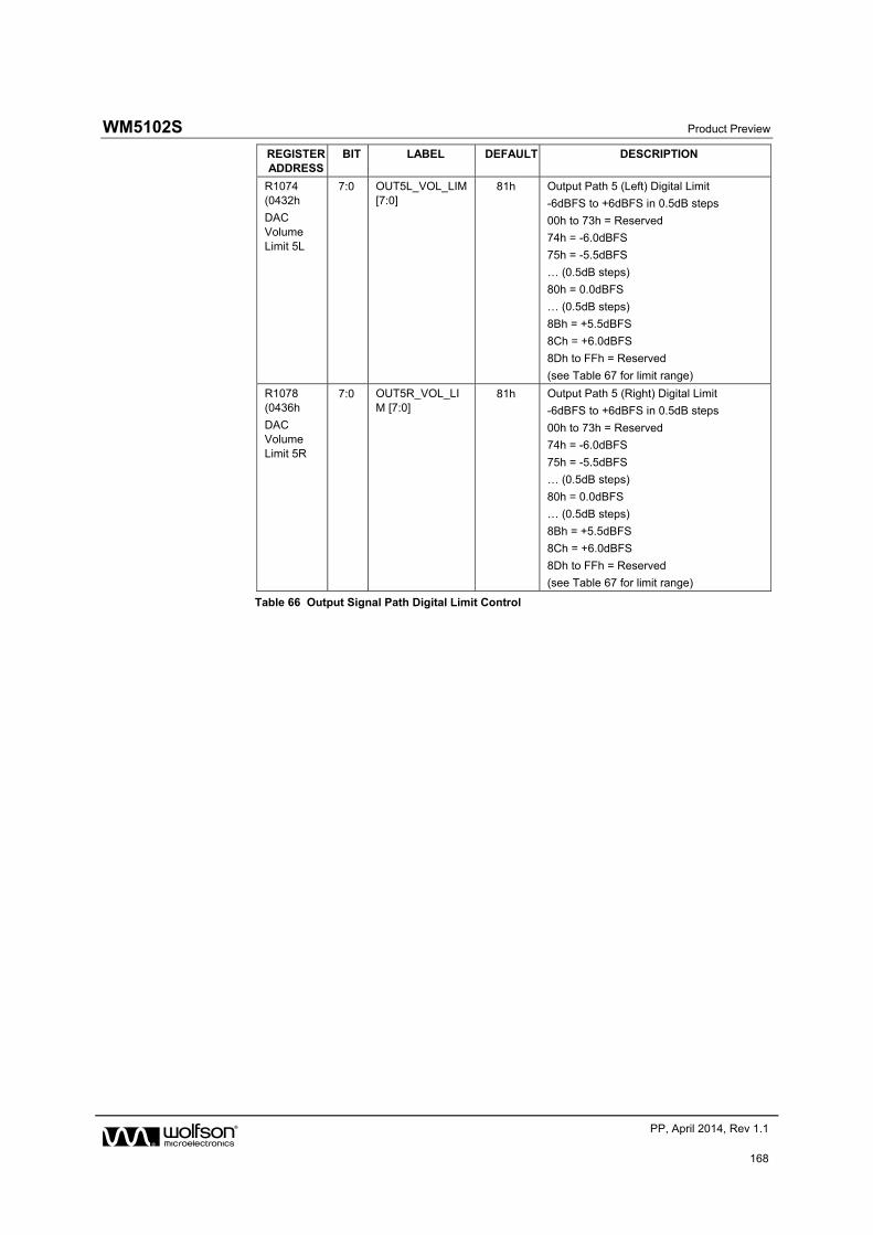
WM5102S Product Preview
w PP, April 2014, Rev 1.1
168
REGISTER ADDRESS
BIT LABEL DEFAULT DESCRIPTION
R1074 (0432h
DAC Volume Limit 5L
7:0 OUT5L_VOL_LIM [7:0]
81h Output Path 5 (Left) Digital Limit
-6dBFS to +6dBFS in 0.5dB steps
00h to 73h = Reserved
74h = -6.0dBFS
75h = -5.5dBFS
… (0.5dB steps)
80h = 0.0dBFS
… (0.5dB steps)
8Bh = +5.5dBFS
8Ch = +6.0dBFS
8Dh to FFh = Reserved
(see Table 67 for limit range)
R1078 (0436h
DAC Volume Limit 5R
7:0 OUT5R_VOL_LIM [7:0]
81h Output Path 5 (Right) Digital Limit
-6dBFS to +6dBFS in 0.5dB steps
00h to 73h = Reserved
74h = -6.0dBFS
75h = -5.5dBFS
… (0.5dB steps)
80h = 0.0dBFS
… (0.5dB steps)
8Bh = +5.5dBFS
8Ch = +6.0dBFS
8Dh to FFh = Reserved
(see Table 67 for limit range)
Table 66 Output Signal Path Digital Limit Control
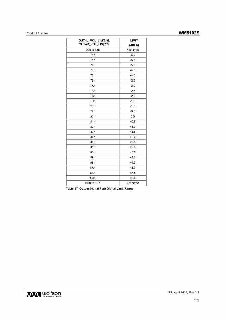
Product Preview WM5102S
w PP, April 2014, Rev 1.1
169
OUTnL_VOL_LIM[7:0], OUTnR_VOL_LIM[7:0]
LIMIT
(dBFS)
00h to 73h Reserved
74h -6.0
75h -5.5
76h -5.0
77h -4.5
78h -4.0
79h -3.5
7Ah -3.0
7Bh -2.5
7Ch -2.0
7Dh -1.5
7Eh -1.0
7Fh -0.5
80h 0.0
81h +0.5
82h +1.0
83h +1.5
84h +2.0
85h +2.5
86h +3.0
87h +3.5
88h +4.0
89h +4.5
8Ah +5.0
8Bh +5.5
8Ch +6.0
8Dh to FFh Reserved
Table 67 Output Signal Path Digital Limit Range
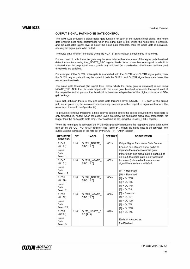
WM5102S Product Preview
w PP, April 2014, Rev 1.1
170
OUTPUT SIGNAL PATH NOISE GATE CONTROL
The WM5102S provides a digital noise gate function for each of the output signal paths. The noise gate ensures best noise performance when the signal path is idle. When the noise gate is enabled, and the applicable signal level is below the noise gate threshold, then the noise gate is activated, causing the signal path to be muted.
The noise gate function is enabled using the NGATE_ENA register, as described in Table 68.
For each output path, the noise gate may be associated with one or more of the signal path threshold detection functions using the _NGATE_SRC register fields. When more than one signal threshold is selected, then the output path noise gate is only activated (ie. muted) when all of the respective signal thresholds are satisfied.
For example, if the OUT1L noise gate is associated with the OUT1L and OUT1R signal paths, then the OUT1L signal path will only be muted if both the OUT1L and OUT1R signal levels are below the respective thresholds.
The noise gate threshold (the signal level below which the noise gate is activated) is set using NGATE_THR. Note that, for each output path, the noise gate threshold represents the signal level at the respective output pin(s) - the threshold is therefore independent of the digital volume and PGA gain settings.
Note that, although there is only one noise gate threshold level (NGATE_THR), each of the output path noise gates may be activated independently, according to the respective signal content and the associated threshold configuration(s).
To prevent erroneous triggering, a time delay is applied before the gate is activated; the noise gate is only activated (ie. muted) when the output levels are below the applicable signal level threshold(s) for longer than the noise gate ‘hold time’. The ‘hold time’ is set using the NGATE_HOLD register.
When the noise gate is activated, the WM5102S gradually attenuates the respective signal path at the rate set by the OUT_VD_RAMP register (see Table 64). When the noise gate is de-activated, the output volume increases at the rate set by the OUT_VI_RAMP register.
REGISTER ADDRESS
BIT LABEL DEFAULT DESCRIPTION
R1043 (0413h)
Noise Gate Select 1L
11:0 OUT1L_NGATE_SRC [11:0]
001h Output Signal Path Noise Gate Source
Enables one of more signal paths as inputs to the respective noise gate.
If more than one signal path is enabled as an input, the noise gate is only activated (ie. muted) when all of the respective signal thresholds are satisfied.
[11] = Reserved
[10] = Reserved
[9] = OUT5R
[8] = OUT5L
[7] = OUT4R
[6] = OUT4L
[5] = Reserved
[4] = OUT3
[3] = OUT2R
[2] = OUT2L
[1] = OUT1R
[0] = OUT1L
Each bit is coded as:
0 = Disabled
R1047 (0417h)
Noise Gate Select 1R
11:0 OUT1R_NGATE_SRC [11:0]
002h
R1051 (041Bh)
Noise Gate Select 2L
11:0 OUT2L_NGATE_SRC [11:0]
004h
R1055 (041Fh)
Noise Gate Select 2R
11:0 OUT2R_NGATE_SRC [11:0]
008h
R1059 (0423h)
Noise Gate Select 3L
11:0 OUT3_NGATE_SRC [11:0]
010h
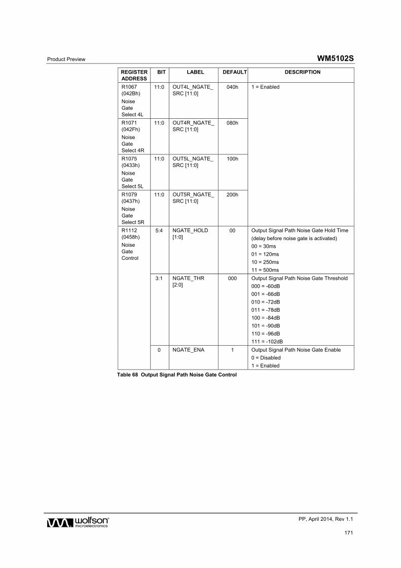
Product Preview WM5102S
w PP, April 2014, Rev 1.1
171
REGISTER ADDRESS
BIT LABEL DEFAULT DESCRIPTION
R1067 (042Bh)
Noise Gate Select 4L
11:0 OUT4L_NGATE_SRC [11:0]
040h 1 = Enabled
R1071 (042Fh)
Noise Gate Select 4R
11:0 OUT4R_NGATE_SRC [11:0]
080h
R1075 (0433h)
Noise Gate Select 5L
11:0 OUT5L_NGATE_SRC [11:0]
100h
R1079 (0437h)
Noise Gate Select 5R
11:0 OUT5R_NGATE_SRC [11:0]
200h
R1112 (0458h)
Noise Gate Control
5:4 NGATE_HOLD [1:0]
00 Output Signal Path Noise Gate Hold Time
(delay before noise gate is activated)
00 = 30ms
01 = 120ms
10 = 250ms
11 = 500ms
3:1 NGATE_THR [2:0]
000 Output Signal Path Noise Gate Threshold
000 = -60dB
001 = -66dB
010 = -72dB
011 = -78dB
100 = -84dB
101 = -90dB
110 = -96dB
111 = -102dB
0 NGATE_ENA 1 Output Signal Path Noise Gate Enable
0 = Disabled
1 = Enabled
Table 68 Output Signal Path Noise Gate Control
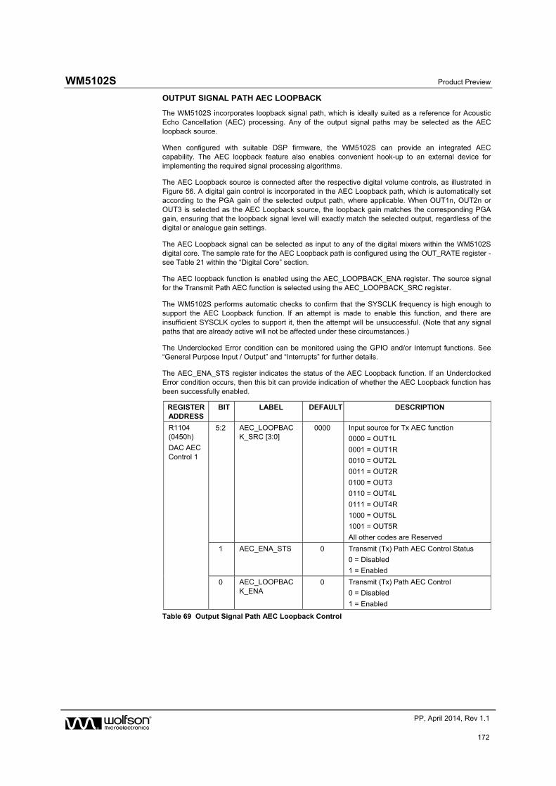
WM5102S Product Preview
w PP, April 2014, Rev 1.1
172
OUTPUT SIGNAL PATH AEC LOOPBACK
The WM5102S incorporates loopback signal path, which is ideally suited as a reference for Acoustic Echo Cancellation (AEC) processing. Any of the output signal paths may be selected as the AEC loopback source.
When configured with suitable DSP firmware, the WM5102S can provide an integrated AEC capability. The AEC loopback feature also enables convenient hook-up to an external device for implementing the required signal processing algorithms.
The AEC Loopback source is connected after the respective digital volume controls, as illustrated in Figure 56. A digital gain control is incorporated in the AEC Loopback path, which is automatically set according to the PGA gain of the selected output path, where applicable. When OUT1n, OUT2n or OUT3 is selected as the AEC Loopback source, the loopback gain matches the corresponding PGA gain, ensuring that the loopback signal level will exactly match the selected output, regardless of the digital or analogue gain settings.
The AEC Loopback signal can be selected as input to any of the digital mixers within the WM5102S digital core. The sample rate for the AEC Loopback path is configured using the OUT_RATE register - see Table 21 within the “Digital Core” section.
The AEC loopback function is enabled using the AEC_LOOPBACK_ENA register. The source signal for the Transmit Path AEC function is selected using the AEC_LOOPBACK_SRC register.
The WM5102S performs automatic checks to confirm that the SYSCLK frequency is high enough to support the AEC Loopback function. If an attempt is made to enable this function, and there are insufficient SYSCLK cycles to support it, then the attempt will be unsuccessful. (Note that any signal paths that are already active will not be affected under these circumstances.)
The Underclocked Error condition can be monitored using the GPIO and/or Interrupt functions. See “General Purpose Input / Output” and “Interrupts” for further details.
The AEC_ENA_STS register indicates the status of the AEC Loopback function. If an Underclocked Error condition occurs, then this bit can provide indication of whether the AEC Loopback function has been successfully enabled.
REGISTER ADDRESS
BIT LABEL DEFAULT DESCRIPTION
R1104 (0450h)
DAC AEC Control 1
5:2 AEC_LOOPBACK_SRC [3:0]
0000 Input source for Tx AEC function
0000 = OUT1L
0001 = OUT1R
0010 = OUT2L
0011 = OUT2R
0100 = OUT3
0110 = OUT4L
0111 = OUT4R
1000 = OUT5L
1001 = OUT5R
All other codes are Reserved
1 AEC_ENA_STS 0 Transmit (Tx) Path AEC Control Status
0 = Disabled
1 = Enabled
0 AEC_LOOPBACK_ENA
0 Transmit (Tx) Path AEC Control
0 = Disabled
1 = Enabled
Table 69 Output Signal Path AEC Loopback Control
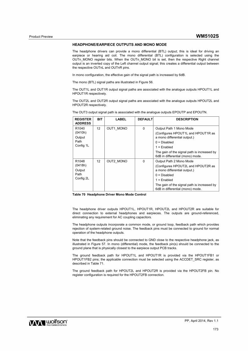
Product Preview WM5102S
w PP, April 2014, Rev 1.1
173
HEADPHONE/EARPIECE OUTPUTS AND MONO MODE
The headphone drivers can provide a mono differential (BTL) output; this is ideal for driving an earpiece or hearing aid coil. The mono differential (BTL) configuration is selected using the OUTn_MONO register bits. When the OUTn_MONO bit is set, then the respective Right channel output is an inverted copy of the Left channel output signal; this creates a differential output between the respective OUTnL and OUTnR pins.
In mono configuration, the effective gain of the signal path is increased by 6dB.
The mono (BTL) signal paths are illustrated in Figure 56.
The OUT1L and OUT1R output signal paths are associated with the analogue outputs HPOUT1L and HPOUT1R respectively.
The OUT2L and OUT2R output signal paths are associated with the analogue outputs HPOUT2L and HPOUT2R respectively.
The OUT3 output signal path is associated with the analogue outputs EPOUTP and EPOUTN.
REGISTER ADDRESS
BIT LABEL DEFAULT DESCRIPTION
R1040 (0410h)
Output Path Config 1L
12 OUT1_MONO 0 Output Path 1 Mono Mode
(Configures HPOUT1L and HPOUT1R as a mono differential output.)
0 = Disabled
1 = Enabled
The gain of the signal path is increased by 6dB in differential (mono) mode.
R1048 (0418h)
Output Path Config 2L
12 OUT2_MONO 0 Output Path 2 Mono Mode
(Configures HPOUT2L and HPOUT2R as a mono differential output.)
0 = Disabled
1 = Enabled
The gain of the signal path is increased by 6dB in differential (mono) mode.
Table 70 Headphone Driver Mono Mode Control
The headphone driver outputs HPOUT1L, HPOUT1R, HPOUT2L and HPOUT2R are suitable for direct connection to external headphones and earpieces. The outputs are ground-referenced, eliminating any requirement for AC coupling capacitors.
The headphone outputs incorporate a common mode, or ground loop, feedback path which provides rejection of system-related ground noise. The feedback pins must be connected to ground for normal operation of the headphone outputs.
Note that the feedback pins should be connected to GND close to the respective headphone jack, as illustrated in Figure 57. In mono (differential) mode, the feedback pin(s) should be connected to the ground plane that is physically closest to the earpiece output PCB tracks.
The ground feedback path for HPOUT1L and HPOUT1R is provided via the HPOUT1FB1 or HPOUT1FB2 pins; the applicable connection must be selected using the ACCDET_SRC register, as described in Table 71.
The ground feedback path for HPOUT2L and HPOUT2R is provided via the HPOUT2FB pin. No register configuration is required for the HPOUT2FB connection.
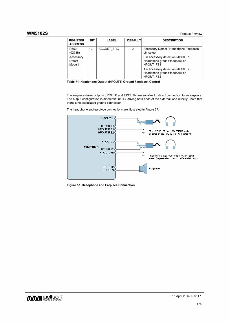
WM5102S Product Preview
w PP, April 2014, Rev 1.1
174
REGISTER ADDRESS
BIT LABEL DEFAULT DESCRIPTION
R659 (0293h)
Accessory Detect Mode 1
13 ACCDET_SRC 0 Accessory Detect / Headphone Feedback pin select
0 = Accessory detect on MICDET1, Headphone ground feedback on HPOUT1FB1
1 = Accessory detect on MICDET2, Headphone ground feedback on HPOUT1FB2
Table 71 Headphone Output (HPOUT1) Ground Feedback Control
The earpiece driver outputs EPOUTP and EPOUTN are suitable for direct connection to an earpiece. The output configuration is differential (BTL), driving both ends of the external load directly - note that there is no associated ground connection.
The headphone and earpiece connections are illustrated in Figure 57.
Figure 57 Headphone and Earpiece Connection
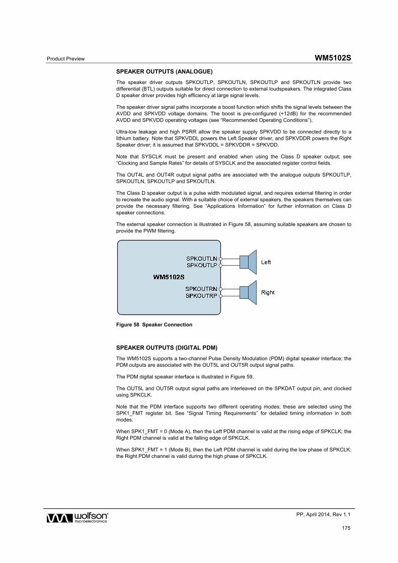
Product Preview WM5102S
w PP, April 2014, Rev 1.1
175
SPEAKER OUTPUTS (ANALOGUE)
The speaker driver outputs SPKOUTLP, SPKOUTLN, SPKOUTLP and SPKOUTLN provide two differential (BTL) outputs suitable for direct connection to external loudspeakers. The integrated Class D speaker driver provides high efficiency at large signal levels.
The speaker driver signal paths incorporate a boost function which shifts the signal levels between the AVDD and SPKVDD voltage domains. The boost is pre-configured (+12dB) for the recommended AVDD and SPKVDD operating voltages (see “Recommended Operating Conditions”).
Ultra-low leakage and high PSRR allow the speaker supply SPKVDD to be connected directly to a lithium battery. Note that SPKVDDL powers the Left Speaker driver, and SPKVDDR powers the Right Speaker driver; it is assumed that SPKVDDL = SPKVDDR = SPKVDD.
Note that SYSCLK must be present and enabled when using the Class D speaker output; see “Clocking and Sample Rates” for details of SYSCLK and the associated register control fields.
The OUT4L and OUT4R output signal paths are associated with the analogue outputs SPKOUTLP, SPKOUTLN, SPKOUTLP and SPKOUTLN.
The Class D speaker output is a pulse width modulated signal, and requires external filtering in order to recreate the audio signal. With a suitable choice of external speakers, the speakers themselves can provide the necessary filtering. See “Applications Information” for further information on Class D speaker connections.
The external speaker connection is illustrated in Figure 58, assuming suitable speakers are chosen to provide the PWM filtering.
Figure 58 Speaker Connection
SPEAKER OUTPUTS (DIGITAL PDM)
The WM5102S supports a two-channel Pulse Density Modulation (PDM) digital speaker interface; the PDM outputs are associated with the OUT5L and OUT5R output signal paths.
The PDM digital speaker interface is illustrated in Figure 59.
The OUT5L and OUT5R output signal paths are interleaved on the SPKDAT output pin, and clocked using SPKCLK.
Note that the PDM interface supports two different operating modes; these are selected using the SPK1_FMT register bit. See “Signal Timing Requirements” for detailed timing information in both modes.
When SPK1_FMT = 0 (Mode A), then the Left PDM channel is valid at the rising edge of SPKCLK; the Right PDM channel is valid at the falling edge of SPKCLK.
When SPK1_FMT = 1 (Mode B), then the Left PDM channel is valid during the low phase of SPKCLK; the Right PDM channel is valid during the high phase of SPKCLK.
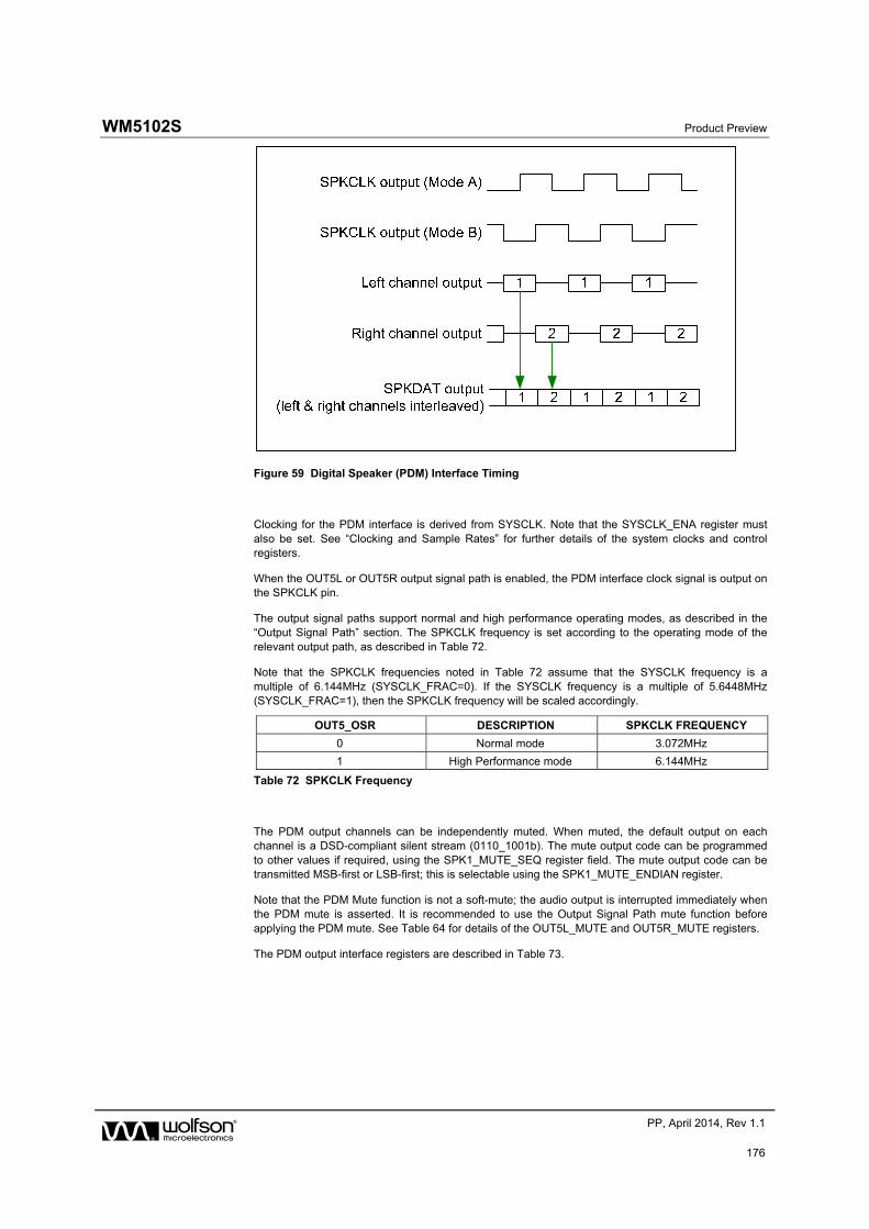
WM5102S Product Preview
w PP, April 2014, Rev 1.1
176
Figure 59 Digital Speaker (PDM) Interface Timing
Clocking for the PDM interface is derived from SYSCLK. Note that the SYSCLK_ENA register must also be set. See “Clocking and Sample Rates” for further details of the system clocks and control registers.
When the OUT5L or OUT5R output signal path is enabled, the PDM interface clock signal is output on the SPKCLK pin.
The output signal paths support normal and high performance operating modes, as described in the “Output Signal Path” section. The SPKCLK frequency is set according to the operating mode of the relevant output path, as described in Table 72.
Note that the SPKCLK frequencies noted in Table 72 assume that the SYSCLK frequency is a multiple of 6.144MHz (SYSCLK_FRAC=0). If the SYSCLK frequency is a multiple of 5.6448MHz (SYSCLK_FRAC=1), then the SPKCLK frequency will be scaled accordingly.
OUT5_OSR DESCRIPTION SPKCLK FREQUENCY
0 Normal mode 3.072MHz
1 High Performance mode 6.144MHz
Table 72 SPKCLK Frequency
The PDM output channels can be independently muted. When muted, the default output on each channel is a DSD-compliant silent stream (0110_1001b). The mute output code can be programmed to other values if required, using the SPK1_MUTE_SEQ register field. The mute output code can be transmitted MSB-first or LSB-first; this is selectable using the SPK1_MUTE_ENDIAN register.
Note that the PDM Mute function is not a soft-mute; the audio output is interrupted immediately when the PDM mute is asserted. It is recommended to use the Output Signal Path mute function before applying the PDM mute. See Table 64 for details of the OUT5L_MUTE and OUT5R_MUTE registers.
The PDM output interface registers are described in Table 73.
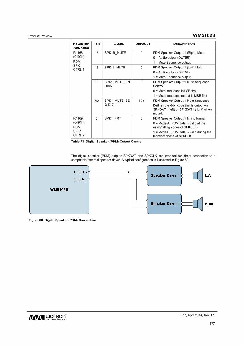
Product Preview WM5102S
w PP, April 2014, Rev 1.1
177
REGISTER ADDRESS
BIT LABEL DEFAULT DESCRIPTION
R1168 (0490h)
PDM SPK1 CTRL 1
13 SPK1R_MUTE 0 PDM Speaker Output 1 (Right) Mute
0 = Audio output (OUT5R)
1 = Mute Sequence output
12 SPK1L_MUTE 0 PDM Speaker Output 1 (Left) Mute
0 = Audio output (OUT5L)
1 = Mute Sequence output
8 SPK1_MUTE_ENDIAN
0 PDM Speaker Output 1 Mute Sequence Control
0 = Mute sequence is LSB first
1 = Mute sequence output is MSB first
7:0 SPK1_MUTE_SEQ [7:0]
69h PDM Speaker Output 1 Mute Sequence
Defines the 8-bit code that is output on SPKDAT1 (left) or SPKDAT1 (right) when muted.
R1169 (0491h)
PDM SPK1 CTRL 2
0 SPK1_FMT 0 PDM Speaker Output 1 timing format
0 = Mode A (PDM data is valid at the rising/falling edges of SPKCLK)
1 = Mode B (PDM data is valid during the high/low phase of SPKCLK)
Table 73 Digital Speaker (PDM) Output Control
The digital speaker (PDM) outputs SPKDAT and SPKCLK are intended for direct connection to a compatible external speaker driver. A typical configuration is illustrated in Figure 60.
Figure 60 Digital Speaker (PDM) Connection
WM5102S Product Preview
w PP, April 2014, Rev 1.1
178
EXTERNAL ACCESSORY DETECTION
The WM5102S provides external accessory detection functions which can sense the presence and impedance of external components. This can be used to detect the insertion or removal of an external headphone or headset, and to provide an indication of key/button push events.
Jack insertion is detected using the JACKDET pin, which must be connected to a switch contact within the jack socket. An Interrupt event is generated whenever a jack insertion or jack removal event is detected. The jack detect function can also be used to trigger a Wake-Up transition (ie. exit from Sleep mode) and/or to trigger the Control Write Sequencer.
Suppression of pops and clicks caused by jack insertion or removal is provided using the MICDET clamp function. This function can also be used to trigger interrupt events, a Wake-Up transition (ie. exit from Sleep mode) and/or to trigger the Control Write Sequencer.
Microphones, push-buttons and other accessories can be detected via the MICDET1 or MICDET2 pins. The presence of a microphone, and the status of a hookswitch can be detected. This feature can also be used to detect push-button operation.
Headphone impedance can be detected via the HPDETL and HPDETR pins; this can be used to set different gain levels or other configuration settings according to the type of load connected. For example, different settings may be applicable to Headphone or Line output loads.
The MICVDD power domain must be enabled when using the Microphone Detect function. (Note that MICVDD is not required for the Jack Detect or Headphone Detect functios.) The MICVDD power domain is provided using an internal Charge Pump (CP2) and LDO Regulator (LDO2). See “Charge Pumps, Regulators and Voltage Reference” for details of these circuits.
The internal 32kHz clock must be present and enabled when using the jack insertion or accessory detection functions; see “Clocking and Sample Rates” for details of the internal 32kHz clock and associated register control fields.
JACK DETECT
The WM5102S provides support for jack insertion switch detection. The jack insertion status can be read using the relevant register status bit. A jack insertion or removal can also be used to trigger an interrupt (IRQ) event or to trigger the Control Write Sequencer.
When the WM5102S is in the low-power Sleep mode (see “Low Power Sleep Configuration”), the jack detect function can be used as a ‘wake-up’ input; a typical use case is where an application is idle in standby mode until a headphone or headset jack is inserted.
Jack insertion and removal is detected using the JACKDET pin. The recommended external connection circuit is illustrated in Figure 61.
The jack detect feature is enabled using JD1_ENA; the jack insertion status can be read using the JD1_STS register.
The JACKDET input de-bounce is selected using the JD1_DB register, as described in Table 74. Note that the de-bounce circuit uses the 32kHz clock, which must be enabled whenever input de-bounce functions are required.
Note that the Jack Detect signal, JD1, can be used as an input to the MICDET Clamp function. This provides additional functionality relating to jack insertion or jack removal events.
An Interrupt Request (IRQ) event is generated whenever a jack insertion or jack removal is detected (see “Interrupts”). Separate ‘mask’ bits are provided to enable IRQ events on the rising and/or falling edge of the JD1 status.
The Control Write Sequencer can be triggered by a jack insertion or jack removal detection. This is enabled using register bits described in the “Low Power Sleep Configuration” section.
The control registers associated with the Jack Detect function are described in Table 74.
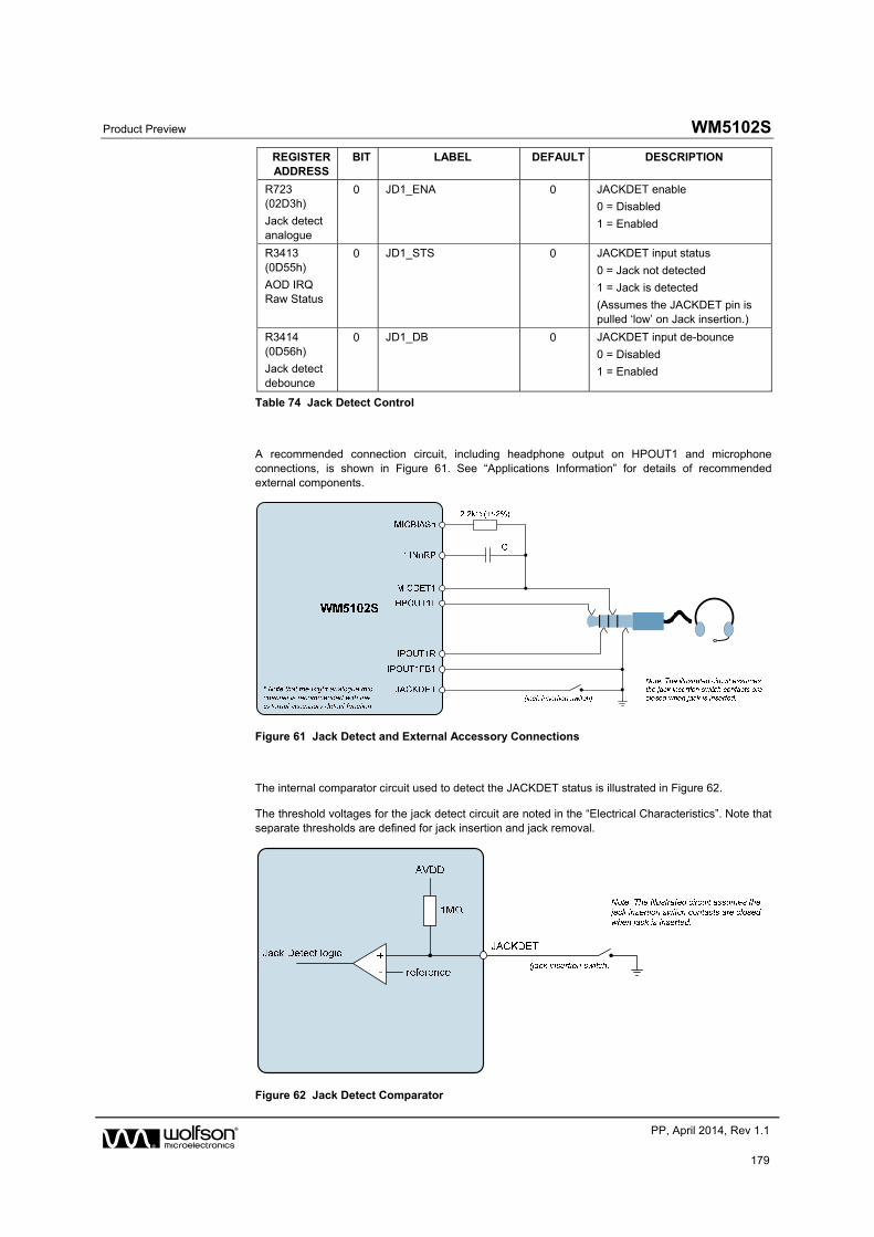
Product Preview WM5102S
w PP, April 2014, Rev 1.1
179
REGISTER ADDRESS
BIT LABEL DEFAULT DESCRIPTION
R723 (02D3h)
Jack detect analogue
0 JD1_ENA 0 JACKDET enable
0 = Disabled
1 = Enabled
R3413 (0D55h)
AOD IRQ Raw Status
0 JD1_STS 0 JACKDET input status
0 = Jack not detected
1 = Jack is detected
(Assumes the JACKDET pin is pulled ‘low’ on Jack insertion.)
R3414 (0D56h)
Jack detect debounce
0 JD1_DB 0 JACKDET input de-bounce
0 = Disabled
1 = Enabled
Table 74 Jack Detect Control
A recommended connection circuit, including headphone output on HPOUT1 and microphone connections, is shown in Figure 61. See “Applications Information” for details of recommended external components.
Figure 61 Jack Detect and External Accessory Connections
The internal comparator circuit used to detect the JACKDET status is illustrated in Figure 62.
The threshold voltages for the jack detect circuit are noted in the “Electrical Characteristics”. Note that separate thresholds are defined for jack insertion and jack removal.
Figure 62 Jack Detect Comparator
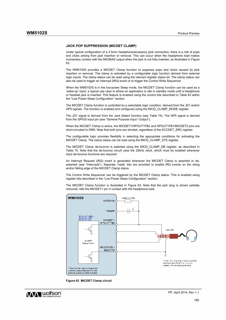
WM5102S Product Preview
w PP, April 2014, Rev 1.1
180
JACK POP SUPPRESSION (MICDET CLAMP)
Under typical configuration of a 3.5mm headphone/accessory jack connection, there is a risk of pops and clicks arising from jack insertion or removal. This can occur when the headphone load makes momentary contact with the MICBIAS output when the jack is not fully inserted, as illustrated in Figure 63.
The WM5102S provides a MICDET Clamp function to suppress pops and clicks caused by jack insertion or removal. The clamp is activated by a configurable logic function derived from external logic inputs. The clamp status can be read using the relevant register status bit. The clamp status can also be used to trigger an interrupt (IRQ) event or to trigger the Control Write Sequencer.
When the WM5102S is in the low-power Sleep mode, the MICDET Clamp function can be used as a ‘wake-up’ input; a typical use case is where an application is idle in standby mode until a headphone or headset jack is inserted. This feature is enabled using the control bits described in Table 83 within the “Low Power Sleep Configuration” section.
The MICDET Clamp function is controlled by a selectable logic condition, derived from the JD1 and/or GP5 signals. The function is enabled and configured using the MICD_CLAMP_MODE register.
The JD1 signal is derived from the Jack Detect function (see Table 74). The GP5 signal is derived from the GPIO5 input pin (see “General Purpose Input / Output”).
When the MICDET Clamp is active, the MICDET1/HPOUT1FB2 and HPOUT1FB1/MICDET2 pins are short-circuited to GND. Note that both pins are shorted, regardless of the ACCDET_SRC register.
The configurable logic provides flexibility in selecting the appropriate conditions for activating the MICDET Clamp. The clamp status can be read using the MICD_CLAMP_STS register.
The MICDET Clamp de-bounce is selected using the MICD_CLAMP_DB register, as described in Table 75. Note that the de-bounce circuit uses the 32kHz clock, which must be enabled whenever input de-bounce functions are required.
An Interrupt Request (IRQ) event is generated whenever the MICDET Clamp is asserted or de-asserted (see “Interrupts”). Separate ‘mask’ bits are provided to enable IRQ events on the rising and/or falling edge of the MICDET Clamp status.
The Control Write Sequencer can be triggered by the MICDET Clamp status. This is enabled using register bits described in the “Low Power Sleep Configuration” section.
The MICDET Clamp function is illustrated in Figure 63. Note that the jack plug is shown partially removed, with the MICDET1 pin in contact with the headphone load.
Figure 63 MICDET Clamp circuit
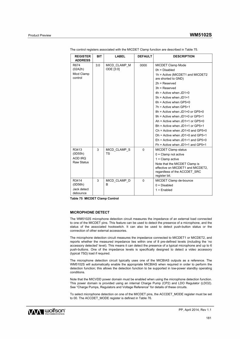
Product Preview WM5102S
w PP, April 2014, Rev 1.1
181
The control registers associated with the MICDET Clamp function are described in Table 75.
REGISTER ADDRESS
BIT LABEL DEFAULT DESCRIPTION
R674 (02A2h)
Micd Clamp control
3:0 MICD_CLAMP_MODE [3:0]
0000 MICDET Clamp Mode
0h = Disabled
1h = Active (MICDET1 and MICDET2 are shorted to GND)
2h = Reserved
3h = Reserved
4h = Active when JD1=0
5h = Active when JD1=1
6h = Active when GP5=0
7h = Active when GP5=1
8h = Active when JD1=0 or GP5=0
9h = Active when JD1=0 or GP5=1
Ah = Active when JD1=1 or GP5=0
Bh = Active when JD1=1 or GP5=1
Ch = Active when JD1=0 and GP5=0
Dh = Active when JD1=0 and GP5=1
Eh = Active when JD1=1 and GP5=0
Fh = Active when JD1=1 and GP5=1
R3413 (0D55h)
AOD IRQ Raw Status
3 MICD_CLAMP_STS
0 MICDET Clamp status
0 = Clamp not active
1 = Clamp active
Note that the MICDET Clamp is effective on MICDET1 and MICDET2, regardless of the ACCDET_SRC register bit.
R3414 (0D56h)
Jack detect debounce
3 MICD_CLAMP_DB
0 MICDET Clamp de-bounce
0 = Disabled
1 = Enabled
Table 75 MICDET Clamp Control
MICROPHONE DETECT
The WM5102S microphone detection circuit measures the impedance of an external load connected to one of the MICDET pins. This feature can be used to detect the presence of a microphone, and the status of the associated hookswitch. It can also be used to detect push-button status or the connection of other external accessories.
The microphone detection circuit measures the impedance connected to MICDET1 or MICDET2, and reports whether the measured impedance lies within one of 8 pre-defined levels (including the ‘no accessory detected’ level). This means it can detect the presence of a typical microphone and up to 6 push-buttons. One of the impedance levels is specifically designed to detect a video accessory (typical 75Ω) load if required.
The microphone detection circuit typically uses one of the MICBIAS outputs as a reference. The WM5102S will automatically enable the appropriate MICBIAS when required in order to perform the detection function; this allows the detection function to be supported in low-power standby operating conditions.
Note that the MICVDD power domain must be enabled when using the microphone detection function. This power domain is provided using an internal Charge Pump (CP2) and LDO Regulator (LDO2). See “Charge Pumps, Regulators and Voltage Reference” for details of these circuits.
To select microphone detection on one of the MICDET pins, the ACCDET_MODE register must be set to 00. The ACCDET_MODE register is defined in Table 76.
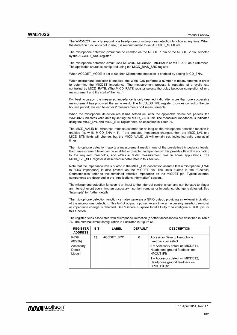
WM5102S Product Preview
w PP, April 2014, Rev 1.1
182
The WM5102S can only support one headphone or microphone detection function at any time. When the detection function is not in use, it is recommended to set ACCDET_MODE=00.
The microphone detection circuit can be enabled on the MICDET1 pin or the MICDET2 pin, selected by the ACCDET_SRC register.
The microphone detection circuit uses MICVDD, MICBIAS1, MICBIAS2 or MICBIAS3 as a reference. The applicable source is configured using the MICD_BIAS_SRC register.
When ACCDET_MODE is set to 00, then Microphone detection is enabled by setting MICD_ENA.
When microphone detection is enabled, the WM5102S performs a number of measurements in order to determine the MICDET impedance. The measurement process is repeated at a cyclic rate controlled by MICD_RATE. (The MICD_RATE register selects the delay between completion of one measurement and the start of the next.)
For best accuracy, the measured impedance is only deemed valid after more than one successive measurement has produced the same result. The MICD_DBTIME register provides control of the de-bounce period; this can be either 2 measurements or 4 measurements.
When the microphone detection result has settled (ie. after the applicable de-bounce period), the WM5102S indicates valid data by setting the MICD_VALID bit. The measured impedance is indicated using the MICD_LVL and MICD_STS register bits, as described in Table 76.
The MICD_VALID bit, when set, remains asserted for as long as the microphone detection function is enabled (ie. while MICD_ENA = 1). If the detected impedance changes, then the MICD_LVL and MICD_STS fields will change, but the MICD_VALID bit will remain set, indicating valid data at all times.
The microphone detection reports a measurement result in one of the pre-defined impedance levels. Each measurement level can be enabled or disabled independently; this provides flexibility according to the required thresholds, and offers a faster measurement time in some applications. The MICD_LVL_SEL register is described in detail later in this section.
Note that the impedance levels quoted in the MICD_LVL description assume that a microphone (475Ω to 30kΩ impedance) is also present on the MICDET pin. The limits quoted in the “Electrical Characteristics” refer to the combined effective impedance on the MICDET pin. Typical external components are described in the “Applications Information” section.
The microphone detection function is an input to the Interrupt control circuit and can be used to trigger an Interrupt event every time an accessory insertion, removal or impedance change is detected. See “Interrupts” for further details.
The microphone detection function can also generate a GPIO output, providing an external indication of the microphone detection. This GPIO output is pulsed every time an accessory insertion, removal or impedance change is detected. See “General Purpose Input / Output” to configure a GPIO pin for this function.
The register fields associated with Microphone Detection (or other accessories) are described in Table 76. The external circuit configuration is illustrated in Figure 64.
REGISTER ADDRESS
BIT LABEL DEFAULT DESCRIPTION
R659 (0293h)
Accessory Detect Mode 1
13 ACCDET_SRC 0 Accessory Detect / Headphone Feedback pin select
0 = Accessory detect on MICDET1, Headphone ground feedback on HPOUT1FB1
1 = Accessory detect on MICDET2, Headphone ground feedback on HPOUT1FB2
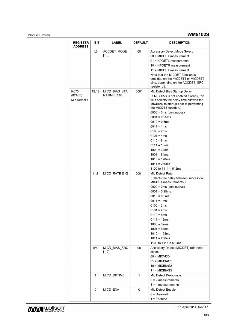
Product Preview WM5102S
w PP, April 2014, Rev 1.1
183
REGISTER ADDRESS
BIT LABEL DEFAULT DESCRIPTION
1:0 ACCDET_MODE [1:0]
00 Accessory Detect Mode Select
00 = MICDET measurement
01 = HPDETL measurement
10 = HPDETR measurement
11 = MICDET measurement
Note that the MICDET function is provided on the MICDET1 or MICDET2 pins, depending on the ACCDET_SRC register bit.
R675 (02A3h)
Mic Detect 1
15:12 MICD_BIAS_STARTTIME [3:0]
0001 Mic Detect Bias Startup Delay
(If MICBIAS is not enabled already, this field selects the delay time allowed for MICBIAS to startup prior to performing the MICDET function.)
0000 = 0ms (continuous)
0001 = 0.25ms
0010 = 0.5ms
0011 = 1ms
0100 = 2ms
0101 = 4ms
0110 = 8ms
0111 = 16ms
1000 = 32ms
1001 = 64ms
1010 = 128ms
1011 = 256ms
1100 to 1111 = 512ms
11:8 MICD_RATE [3:0] 0001 Mic Detect Rate
(Selects the delay between successive MICDET measurements.)
0000 = 0ms (continuous)
0001 = 0.25ms
0010 = 0.5ms
0011 = 1ms
0100 = 2ms
0101 = 4ms
0110 = 8ms
0111 = 16ms
1000 = 32ms
1001 = 64ms
1010 = 128ms
1011 = 256ms
1100 to 1111 = 512ms
5:4 MICD_BIAS_SRC [1:0]
00 Accessory Detect (MICDET) reference select
00 = MICVDD
01 = MICBIAS1
10 = MICBIAS2
11 = MICBIAS3
1 MICD_DBTIME 1 Mic Detect De-bounce
0 = 2 measurements
1 = 4 measurements
0 MICD_ENA 0 Mic Detect Enable
0 = Disabled
1 = Enabled
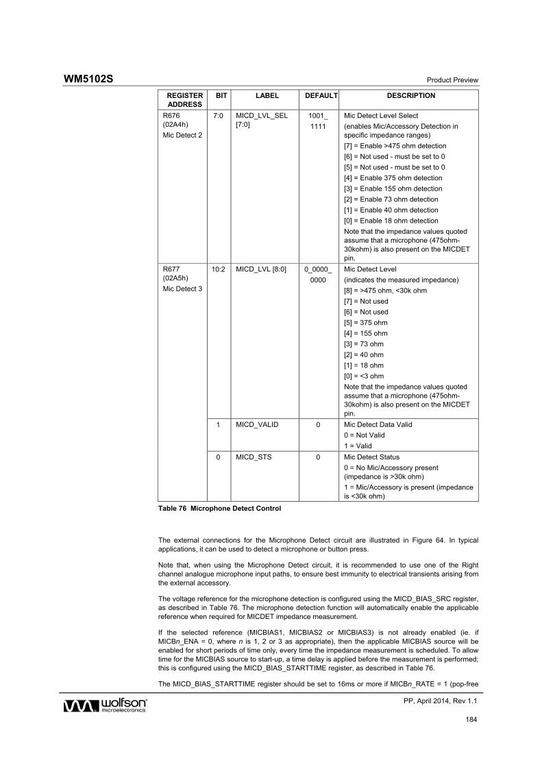
WM5102S Product Preview
w PP, April 2014, Rev 1.1
184
REGISTER ADDRESS
BIT LABEL DEFAULT DESCRIPTION
R676 (02A4h)
Mic Detect 2
7:0 MICD_LVL_SEL [7:0]
1001_
1111
Mic Detect Level Select
(enables Mic/Accessory Detection in specific impedance ranges)
[7] = Enable >475 ohm detection
[6] = Not used - must be set to 0
[5] = Not used - must be set to 0
[4] = Enable 375 ohm detection
[3] = Enable 155 ohm detection
[2] = Enable 73 ohm detection
[1] = Enable 40 ohm detection
[0] = Enable 18 ohm detection
Note that the impedance values quoted assume that a microphone (475ohm-30kohm) is also present on the MICDET pin.
R677 (02A5h)
Mic Detect 3
10:2 MICD_LVL [8:0] 0_0000_
0000
Mic Detect Level
(indicates the measured impedance)
[8] = >475 ohm, <30k ohm
[7] = Not used
[6] = Not used
[5] = 375 ohm
[4] = 155 ohm
[3] = 73 ohm
[2] = 40 ohm
[1] = 18 ohm
[0] = <3 ohm
Note that the impedance values quoted assume that a microphone (475ohm-30kohm) is also present on the MICDET pin.
1 MICD_VALID 0 Mic Detect Data Valid
0 = Not Valid
1 = Valid
0 MICD_STS 0 Mic Detect Status
0 = No Mic/Accessory present (impedance is >30k ohm)
1 = Mic/Accessory is present (impedance is <30k ohm)
Table 76 Microphone Detect Control
The external connections for the Microphone Detect circuit are illustrated in Figure 64. In typical applications, it can be used to detect a microphone or button press.
Note that, when using the Microphone Detect circuit, it is recommended to use one of the Right channel analogue microphone input paths, to ensure best immunity to electrical transients arising from the external accessory.
The voltage reference for the microphone detection is configured using the MICD_BIAS_SRC register, as described in Table 76. The microphone detection function will automatically enable the applicable reference when required for MICDET impedance measurement.
If the selected reference (MICBIAS1, MICBIAS2 or MICBIAS3) is not already enabled (ie. if MICBn_ENA = 0, where n is 1, 2 or 3 as appropriate), then the applicable MICBIAS source will be enabled for short periods of time only, every time the impedance measurement is scheduled. To allow time for the MICBIAS source to start-up, a time delay is applied before the measurement is performed; this is configured using the MICD_BIAS_STARTTIME register, as described in Table 76.
The MICD_BIAS_STARTTIME register should be set to 16ms or more if MICBn_RATE = 1 (pop-free
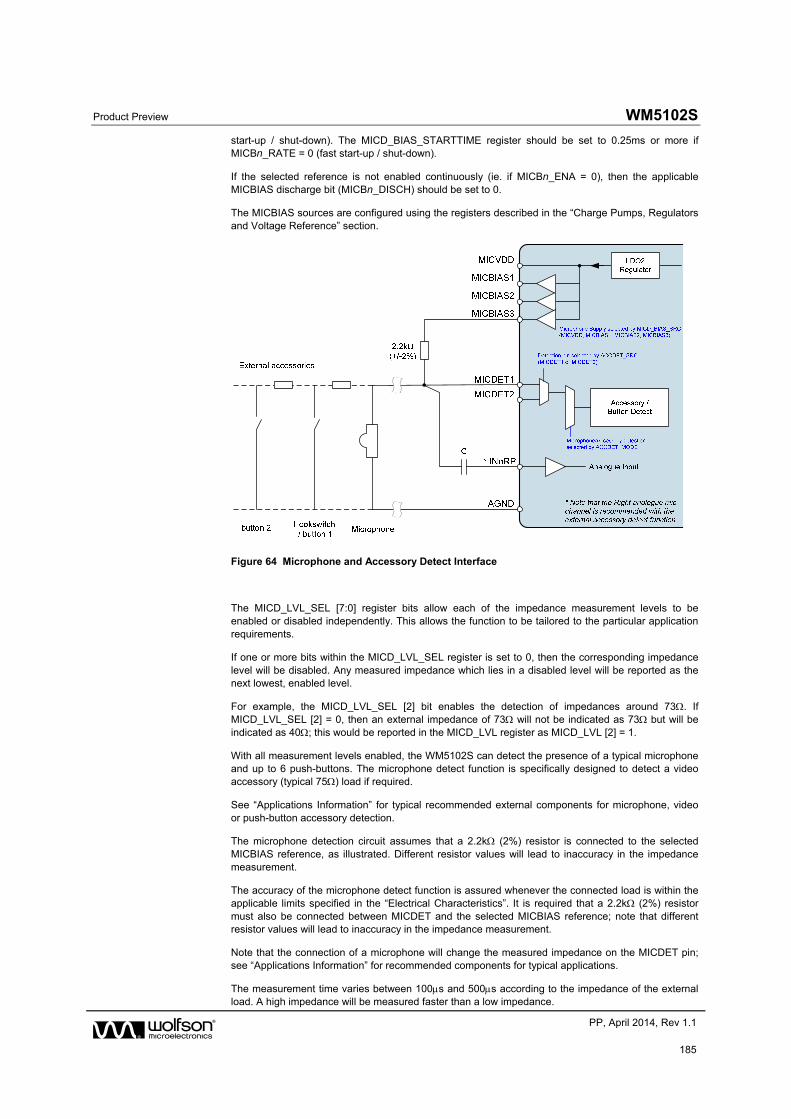
Product Preview WM5102S
w PP, April 2014, Rev 1.1
185
start-up / shut-down). The MICD_BIAS_STARTTIME register should be set to 0.25ms or more if MICBn_RATE = 0 (fast start-up / shut-down).
If the selected reference is not enabled continuously (ie. if MICBn_ENA = 0), then the applicable MICBIAS discharge bit (MICBn_DISCH) should be set to 0.
The MICBIAS sources are configured using the registers described in the “Charge Pumps, Regulators and Voltage Reference” section.
Figure 64 Microphone and Accessory Detect Interface
The MICD_LVL_SEL [7:0] register bits allow each of the impedance measurement levels to be enabled or disabled independently. This allows the function to be tailored to the particular application requirements.
If one or more bits within the MICD_LVL_SEL register is set to 0, then the corresponding impedance level will be disabled. Any measured impedance which lies in a disabled level will be reported as the next lowest, enabled level.
For example, the MICD_LVL_SEL [2] bit enables the detection of impedances around 73. If MICD_LVL_SEL [2] = 0, then an external impedance of 73 will not be indicated as 73 but will be indicated as 40; this would be reported in the MICD_LVL register as MICD_LVL [2] = 1.
With all measurement levels enabled, the WM5102S can detect the presence of a typical microphone and up to 6 push-buttons. The microphone detect function is specifically designed to detect a video accessory (typical 75) load if required.
See “Applications Information” for typical recommended external components for microphone, video or push-button accessory detection.
The microphone detection circuit assumes that a 2.2k (2%) resistor is connected to the selected MICBIAS reference, as illustrated. Different resistor values will lead to inaccuracy in the impedance measurement.
The accuracy of the microphone detect function is assured whenever the connected load is within the applicable limits specified in the “Electrical Characteristics”. It is required that a 2.2k (2%) resistor must also be connected between MICDET and the selected MICBIAS reference; note that different resistor values will lead to inaccuracy in the impedance measurement.
Note that the connection of a microphone will change the measured impedance on the MICDET pin; see “Applications Information” for recommended components for typical applications.
The measurement time varies between 100s and 500s according to the impedance of the external load. A high impedance will be measured faster than a low impedance.
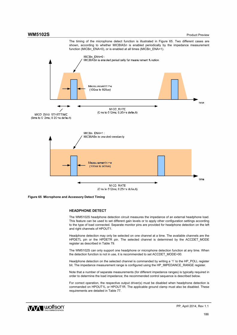
WM5102S Product Preview
w PP, April 2014, Rev 1.1
186
The timing of the microphone detect function is illustrated in Figure 65. Two different cases are shown, according to whether MICBIASn is enabled periodically by the impedance measurement function (MICBn_ENA=0), or is enabled at all times (MICBn_ENA=1).
Figure 65 Microphone and Accessory Detect Timing
HEADPHONE DETECT
The WM5102S headphone detection circuit measures the impedance of an external headphone load. This feature can be used to set different gain levels or to apply other configuration settings according to the type of load connected. Separate monitor pins are provided for headphone detection on the left and right channels of HPOUT1.
Headphone detection may only be selected on one channel at a time. The available channels are the HPDETL pin or the HPDETR pin. The selected channel is determined by the ACCDET_MODE register as described in Table 79.
The WM5102S can only support one headphone or microphone detection function at any time. When the detection function is not in use, it is recommended to set ACCDET_MODE=00.
Headphone detection on the selected channel is commanded by writing a ‘1’ to the HP_POLL register bit. The impedance measurement range is configured using the HP_IMPEDANCE_RANGE register.
Note that a number of separate measurements (for different impedance ranges) is typically required in order to determine the load impedance; the recommended control sequence is described below.
For correct operation, the respective output driver(s) must be disabled when headphone detection is commanded on HPOUT1L or HPOUT1R. The applicable ground clamp must also be disabled. These requirements are detailed in Table 77.
Product Preview WM5102S
w PP, April 2014, Rev 1.1
187
The HP1L_ENA and HP1R_ENA register bits are defined in Table 59. The RMV_SHRT_HP1L and RMV_SHRT_HP1R register bits are defined in Table 79.
Note that, when configuring the RMV_SHRT_HP1L or RMV_SHRT_HP1R bits, care is required not to change the value of other bits in the register, which may have changed from the default setting. Accordingly, a ‘read-modify-write’ sequence is required to implement this.
The applicable headphone output(s) configuration must be maintained until after the headphone detection has completed.
DESCRIPTION REQUIREMENT
Impedance measurement on HPOUT1L HP1L_ENA = 0
RMV_SHRT_HP1L = 1
Impedance measurement on HPOUT1R HP1R_ENA = 0
RMV_SHRT_HP1R = 1
Table 77 Output Configuration for Headphone Detect
When headphone detection is commanded, the WM5102S uses an adjustable current source to determine the connected impedance. A sweep of measurement currents is applied. The rate of this sweep can be adjusted using the HP_RATE register. To avoid audible clicks, the default step size should always be used (HP_RATE = 0).
The timing of the current source ramp is also controlled by the HP_HOLDTIME register. It is recommended that the default setting (001b) be used for this parameter.
Completion of each measurement is indicated by the HP_DONE register bit. When this bit is set, the measurement result can be read from the HP_DACVAL register. Note that the decoding equation of this register (to convert into ‘ohms’) varies according to the HP_IMPEDANCE_RANGE setting.
HEADPHONE IMPEDANCE MEASUREMENT
1 Trigger the HP measurement, with HP_IMPEDANCE_RANGE = 00
2 If the HP_DACVAL result >= 100, then decode the impedance as follows:
Otherwise, proceed to step 3.
3 Trigger the HP measurement, with HP_IMPEDANCE_RANGE = 01
4 If the HP_DACVAL result >= 169, then decode the impedance as follows:
Otherwise, proceed to step 5.
5 Trigger the HP measurement, with HP_IMPEDANCE_RANGE = 10
6 If the HP_DACVAL result >= 169, then decode the impedance as follows:
Otherwise, the impedance is out of range (too high).
Table 78 Headphone Impedance Measurement Control Sequence
Each measurement is triggered by writing ‘1’ to the HP_POLL bit. Completion of each measurement is indicated by the HP_DONE register bit. Note that, after the HP_DONE bit has been asserted, it will remain asserted until the next measurement has been commanded.
The headphone detection function is an input to the Interrupt control circuit and can be used to trigger an Interrupt event on completion of the headphone detection - see “Interrupts”.
WM5102S Product Preview
w PP, April 2014, Rev 1.1
188
The headphone detection function can also generate a GPIO output, providing an external indication of the headphone detection. See “General Purpose Input / Output” to configure a GPIO pin for this function.
The register fields associated with Headphone Detection are described in Table 79. The external circuit configuration is illustrated in Figure 66.
REGISTER ADDRESS
BIT LABEL DEFAULT DESCRIPTION
R549 (0225h)
HP Ctrl 1L
14 RMV_SHRT_HP1L
0 HPOUT1L Ground Clamp
0 = Enabled
1 = Disabled
This bit must be set to 1 when the Headphone Detection function is enabled on HPOUT1L.
This bit is configured automatically when HPOUT1L is enabled or disabled.
R550 (0226h)
HP Ctrl 1R
14 RMV_SHRT_HP1R
0 HPOUT1R Ground Clamp
0 = Enabled
1 = Disabled
This bit must be set to 1 when the Headphone Detection function is enabled on HPOUT1R.
This bit is configured automatically when HPOUT1R is enabled or disabled.
R659 (0293h)
Accessory Detect Mode 1
1:0 ACCDET_MODE [1:0]
00 Accessory Detect Mode Select
00 = MICDET measurement
01 = HPDETL measurement
10 = HPDETR measurement
11 = MICDET
Note that the MICDET function is provided on the MICDET1 or MICDET2 pins, depending on the ACCDET_SRC register bit.
R667 (029Bh)
Headphone Detect 1
10:9 HP_IMPEDANCE_RANGE [1:0]
00 Headphone Detect Range
00 = 4 ohms to 80 ohms
01 = 70 ohms to 1k ohms
10 = 1k ohms to 10k ohms
11 = Reserved
7:5 HP_HOLDTIME [2:0]
001 Headphone Detect Hold Time
(Selects the hold time between ramp up and ramp down of the headphone detect current source.)
000 = 31.25us
001 = 125us
010 = 500us
011 = 2ms
100 = 8ms
101 = 16ms
110 = 24ms
111 = 32ms
1 HP_RATE 0 Headphone Detect Ramp Rate
0 = Normal rate
1 = Fast rate
0 HP_POLL 0 Headphone Detect Enable
Write 1 to start HP Detect function
R668 (029Ch)
Headphone Detect 2
15 HP_DONE 0 Headphone Detect Status
0 = HP Detect not complete
1 = HP Detect done
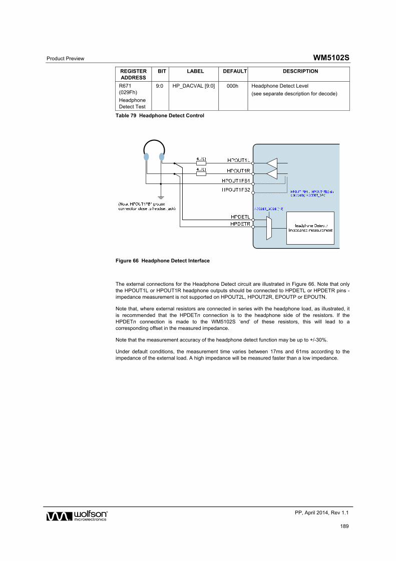
Product Preview WM5102S
w PP, April 2014, Rev 1.1
189
REGISTER ADDRESS
BIT LABEL DEFAULT DESCRIPTION
R671 (029Fh)
Headphone Detect Test
9:0 HP_DACVAL [9:0] 000h Headphone Detect Level
(see separate description for decode)
Table 79 Headphone Detect Control
Figure 66 Headphone Detect Interface
The external connections for the Headphone Detect circuit are illustrated in Figure 66. Note that only the HPOUT1L or HPOUT1R headphone outputs should be connected to HPDETL or HPDETR pins - impedance measurement is not supported on HPOUT2L, HPOUT2R, EPOUTP or EPOUTN.
Note that, where external resistors are connected in series with the headphone load, as illustrated, it is recommended that the HPDETn connection is to the headphone side of the resistors. If the HPDETn connection is made to the WM5102S ‘end’ of these resistors, this will lead to a corresponding offset in the measured impedance.
Note that the measurement accuracy of the headphone detect function may be up to +/-30%.
Under default conditions, the measurement time varies between 17ms and 61ms according to the impedance of the external load. A high impedance will be measured faster than a low impedance.
WM5102S Product Preview
w PP, April 2014, Rev 1.1
190
LOW POWER SLEEP CONFIGURATION
The WM5102S supports a low-power ‘Sleep’ mode, where most functions are disabled, and power consumption is minimised. A selectable ‘Wake-Up’ event can be configured to return the device to full operation and/or execute a specific response to the particular Wake-Up condition.
A Wake-Up event is triggered via hardware input pin(s); in typical applications, these inputs are associated with jack insert (via the JACKDET analogue input) or external push-button detection (via the GPIO5 digital input). A Wake-Up transition can also be triggered using the LDOENA pin to enable LDO1 (assuming that DCVDD is supplied by LDO1).
The WM5102S enters Sleep mode when LDO1 is disabled, causing the DCVDD supply to be removed. The AVDD, DBVDD1, and LDOVDD supplies must be present throughout the Sleep mode duration.
Note that it is assumed that DCVDD is supplied by LDO1; see “Charge Pumps, Regulators and Voltage Reference” for specific control requirements where DCVDD is not powered from LDO1.
SLEEP MODE
The WM5102S enters Sleep mode when LDO1 is disabled, causing the DCVDD supply to be removed; (LDO1 can be controlled using the LDO1_ENA register bit, or using the LDOENA pin; both of these controls must be de-asserted to disable the LDO.) The AVDD, DBVDD1, and LDOVDD supplies must be present throughout the Sleep mode; under these conditions, and with LDO1 disabled, most of the Digital Core (and control registers) are held in reset.
Note that it is assumed that DCVDD is supplied by LDO1; see “Charge Pumps, Regulators and Voltage Reference” for specific control requirements where DCVDD is not powered from LDO1.
The system clocks (SYSCLK, ASYNCCLK) are not required in Sleep mode, and the external clock inputs (MCLKn) may be stopped, except as described below.
If de-bounce is enabled on any of the configured Wake-Up signals (JACKDET or GPIO5), then the 32kHz clock must be active during Sleep mode (see “Clocking and Sample Rates”). The 32kHz clock must be derived from the MCLK2 pin in this case. The 32kHz clock must be configured using CLK_32K_ENA and CLK_32K_SRC before Sleep mode is entered.
The MCLK2 frequency limit in Sleep mode (see “Signal Timing Requirements”) must be observed before entering Sleep mode, and maintained until after Wake-Up.
Selected functions and control registers are maintained via an ‘Always-On’ internal supply domain in Sleep mode. The ‘Always-On’ control registers are listed in Table 80. These registers are maintained (ie. not reset) in Sleep mode.
Note that the Control Interface is not supported in Sleep mode. Read/Write access to the ‘Always-On’ registers is not possible in Sleep mode.
REGISTER ADDRESS
LABEL REFERENCE
40h WKUP_MICD_CLAMP_FALL See Table 83
WKUP_MICD_CLAMP_RISE
WKUP_GP5_FALL
WKUP_GP5_RISE
WKUP_JD1_FALL
WKUP_JD1_RISE
41h WSEQ_ENA_MICD_CLAMP_FALL
See Table 84
WSEQ_ENA_MICD_CLAMP_RISE
WSEQ_ENA_GP5_FALL
WSEQ_ENA_GP5_RISE
WSEQ_ENA_JD1_FALL
WSEQ_ENA_JD1_RISE
Product Preview WM5102S
w PP, April 2014, Rev 1.1
191
REGISTER ADDRESS
LABEL REFERENCE
66h WSEQ_MICD_CLAMP_RISE_INDEX
See “Control Write Sequencer”
67h WSEQ_MICD_CLAMP_FALL_INDEX
68h WSEQ_GP5_RISE_INDEX
69h WSEQ_GP5_FALL_INDEX
6Ah WSEQ_JD1_RISE_INDEX
6Bh WSEQ_JD1_FALL_INDEX
100h CLK_32K_ENA See “Clocking and Sample Rates”
CLK_32K_SRC
210h LDO1_VSEL See “Charge Pumps, Regulators and Voltage Reference” LDO1_DISCH
LDO1_BYPASS
LDO1_ENA
02A2h MICD_CLAMP_MODE See “External Accessory Detection”
02D3h JD1_ENA See “External Accessory Detection”
0C04h GP5_DIR See “General Purpose Input / Output”
GP5_PU
GP5_PD
GP5_POL
GP5_OP_CFG
GP5_DB
GP5_LVL
GP5_FN
0C0Fh IRQ_POL See “Interrupts”
IRQ_OP_CFG
0C10h GP_DBTIME See “General Purpose Input / Output”
0C20h LDO1ENA_PD See “Charge Pumps, Regulators and Voltage Reference”
MCLK2_PD See “Clocking and Sample Rates”
RESET_PU See “Software Reset, Wake-Up, and Device ID”
0D0Fh IM_IRQ1 See “Interrupts”
0D1Fh IM_IRQ2
0D50h MICD_CLAMP_FALL_TRIG_STS See Table 82
MICD_CLAMP_RISE_TRIG_STS
GP5_FALL_TRIG_STS
GP5_RISE_TRIG_STS
JD1_FALL_TRIG_STS
JD1_RISE_TRIG_STS
0D51h MICD_CLAMP_FALL_EINT1 See “Interrupts”
MICD_CLAMP_RISE_EINT1
GP5_FALL_EINT1
GP5_RISE_EINT1
JD1_FALL_EINT1
JD1_RISE_EINT1
0D52h MICD_CLAMP_FALL_EINT2 See “Interrupts”
MICD_CLAMP_RISE_EINT2
GP5_FALL_EINT2
GP5_RISE_EINT2
JD1_FALL_EINT2
JD1_RISE_EINT2

WM5102S Product Preview
w PP, April 2014, Rev 1.1
192
REGISTER ADDRESS
LABEL REFERENCE
0D53h IM_MICD_CLAMP_FALL_EINT1 See “Interrupts”
IM_MICD_CLAMP_RISE_EINT1
IM_GP5_FALL_EINT1
IM_GP5_RISE_EINT1
IM_JD1_FALL_EINT1
IM_JD1_RISE_EINT1
0D54h IM_MICD_CLAMP_FALL_EINT2 See “Interrupts”
IM_MICD_CLAMP_RISE_EINT2
IM_GP5_FALL_EINT2
IM_GP5_RISE_EINT2
IM_JD1_FALL_EINT2
IM_JD1_RISE_EINT2
0D56h MICD_CLAMP_DB See “External Accessory Detection”
JD1_DB
3000h to 31FFh
WSEQ_DATA_WIDTHn See “Control Write Sequencer”
WSEQ_ADDRn
WSEQ_DELAYn
WSEQ_DATA_STARTn
WSEQ_DATAn
Table 80 Sleep Mode ‘Always-On’ Control Registers
The ‘Always-On’ digital input / output pins are listed in Table 81. All other digital input pins will have no effect in Sleep mode. The IRQ¯¯¯ output is normally de-asserted in Sleep mode.
Note that, in Sleep mode, the IRQ¯¯¯ output can only be asserted in response to the JD1 or GP5 control signals (these described in the following section). If the IRQ¯¯¯ output is asserted in Sleep mode, it can only be de-asserted after a Wake-Up transition.
PIN NAME DESCRIPTION REFERENCE
LDOENA Enable pin for LDO1 See “Charge Pumps, Regulators and Voltage Reference”
RESET¯¯¯¯¯¯ Digital Reset input (active low) See “Software Reset, Wake-Up, and Device ID”
MCLK2 Master clock 2 See “Clocking and Sample Rates”
GPIO5 General Purpose pin GPIO5 See “General Purpose Input / Output”
IRQ¯¯¯ Interrupt Request (IRQ) output See “Interrupts”
Table 81 Sleep Mode ‘Always-On’ Digital Input Pins
A Wake-Up transition is triggered using the JD1 or GP5 control signals (defined below).
It is assumed that DCVDD is supplied by LDO1. The AVDD, DBVDD1 and LDOVDD supplies must be present throughout the Sleep mode duration. See “Charge Pumps, Regulators and Voltage Reference” for specific control requirements where DCVDD is not powered from LDO1.
Note that a logic ‘1’ applied to the LDOENA pin will also cause a Wake-Up transition. In this event, however, the configurable Wake-Up events (described below) are not applicable.
Product Preview WM5102S
w PP, April 2014, Rev 1.1
193
SLEEP CONTROL SIGNALS - JD1, GP5, MICDET CLAMP
The internal control signals JD1 and GP5 are provided to support the low-power Sleep mode. The MICDET Clamp status is controlled by a selectable logic function, derived from JD1 and/or GP5. A rising or falling edge of these signals can be used to trigger a Wake-Up transition (ie. exit from Sleep mode).
The JD1, GP5 and MICDET Clamp status signals can also be used to trigger the Control Write Sequencer and/or the Interrupt Controller.
Note that it is not possible to trigger the Control Write Sequencer from the same event used to trigger a Wake-Up transition. (This is because SYSCLK is disabled following a Wake-Up transition; a valid SYSCLK must be enabled before triggering the Control Write Sequencer.)
The JD1, GP5 and MICDET Clamp status signals are described in this section. The Wake-Up, Write Sequencer, and Interrupt actions are described in the sections that follow.
The JD1 signal is derived from the Jack Detect function (see “External Accessory Detection”). This input can be used to trigger Wake-Up or other actions in response to a jack insertion or jack removal detection.
When the JD1 signal is enabled, it indicates the status of the JACKDET input pin. See Table 74 for details of the associated control registers.
The GP5 signal is derived from the GPIO5 input pin (see “General Purpose Input / Output”). This input can be used to trigger Wake-Up or other actions in response to a logic level input detected on the GPIO5 pin.
When using the GP5 signal, the GPIO5 pin must be configured as a GPIO input (GP5_DIR=1, GP5_FN=01h). An internal pull-up or pull-down resistor may be enabled on the GPIO5 pin if required.
The GPIO pin control registers are defined in Table 85.
The MICDET Clamp status is controlled by the JD1 and/or GP5 signals (see “External Accessory Detection”). The configurable logic provides flexibility in selecting the appropriate conditions for activating the MICDET Clamp. The clamp status can be used to trigger Wake-Up or other actions in response to a jack insertion or jack removal detection.
The MICDET Clamp function is configured using the MICD_CLAMP_MODE register, as described in Table 75.
Whenever a rising or falling edge is detected on JD1, GP5 or MICDET Clamp status, the WM5102S will assert the respective trigger status (_TRIG_STS) bit. The trigger status bits are latching fields and, once they are set, they are not reset until a ‘1’ is written to the respective register bit(s).
The JD1, GP5 and MICDET Clamp trigger status bits are described in Table 82.
The trigger status bits can be used to control Wake-Up and Write Sequencer actions. The JD1, GP5 and MICDET Clamp signals are inputs to the Interrupt Controller. Each of these functions is described in the following sections.
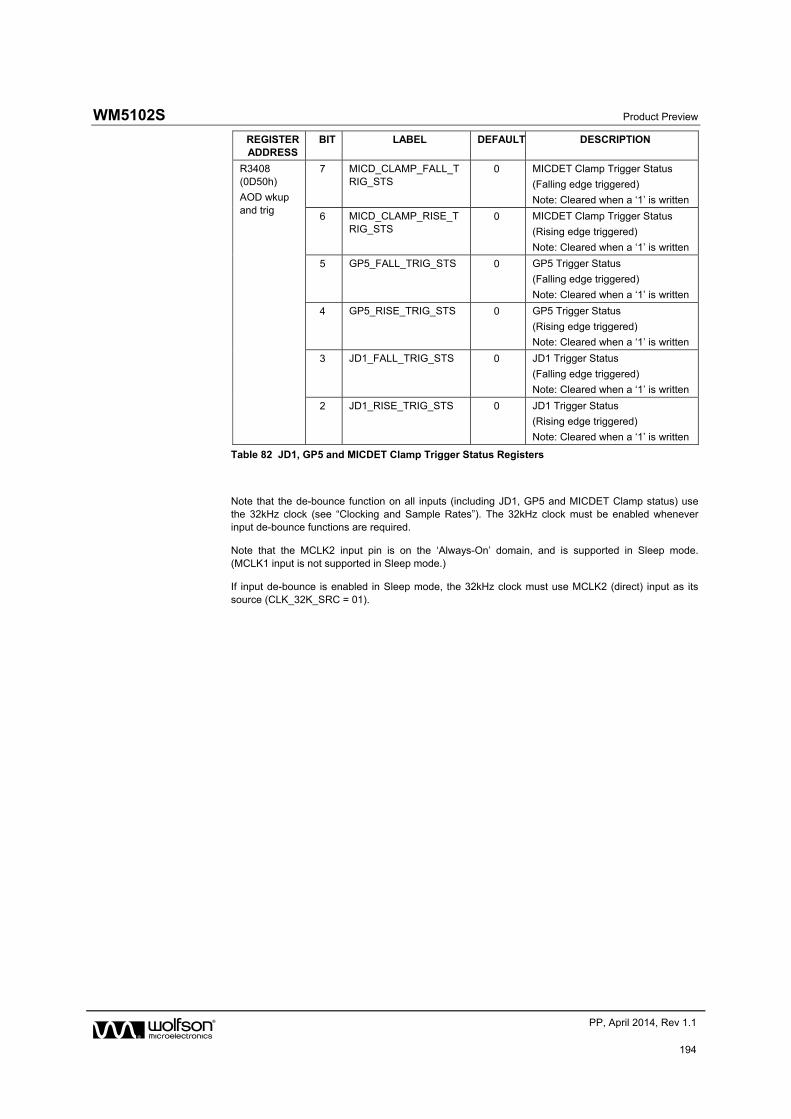
WM5102S Product Preview
w PP, April 2014, Rev 1.1
194
REGISTER ADDRESS
BIT LABEL DEFAULT DESCRIPTION
R3408 (0D50h)
AOD wkup and trig
7 MICD_CLAMP_FALL_TRIG_STS
0 MICDET Clamp Trigger Status
(Falling edge triggered)
Note: Cleared when a ‘1’ is written
6 MICD_CLAMP_RISE_TRIG_STS
0 MICDET Clamp Trigger Status
(Rising edge triggered)
Note: Cleared when a ‘1’ is written
5 GP5_FALL_TRIG_STS 0 GP5 Trigger Status
(Falling edge triggered)
Note: Cleared when a ‘1’ is written
4 GP5_RISE_TRIG_STS 0 GP5 Trigger Status
(Rising edge triggered)
Note: Cleared when a ‘1’ is written
3 JD1_FALL_TRIG_STS 0 JD1 Trigger Status
(Falling edge triggered)
Note: Cleared when a ‘1’ is written
2 JD1_RISE_TRIG_STS 0 JD1 Trigger Status
(Rising edge triggered)
Note: Cleared when a ‘1’ is written
Table 82 JD1, GP5 and MICDET Clamp Trigger Status Registers
Note that the de-bounce function on all inputs (including JD1, GP5 and MICDET Clamp status) use the 32kHz clock (see “Clocking and Sample Rates”). The 32kHz clock must be enabled whenever input de-bounce functions are required.
Note that the MCLK2 input pin is on the ‘Always-On’ domain, and is supported in Sleep mode. (MCLK1 input is not supported in Sleep mode.)
If input de-bounce is enabled in Sleep mode, the 32kHz clock must use MCLK2 (direct) input as its source (CLK_32K_SRC = 01).

Product Preview WM5102S
w PP, April 2014, Rev 1.1
195
WAKE-UP TRANSITION
A Wake-Up transition (exit from Sleep) can be associated with any of the JD1, GP5 or MICDET Clamp trigger status bits. This is selected using the register bits described in Table 83.
REGISTER ADDRESS
BIT LABEL DEFAULT DESCRIPTION
R64 (0040h)
Wake Control
7 WKUP_MICD_CLAMP_FALL
0 MICDET Clamp (Falling) Wake-Up Select
0 = Disabled
1 = Enabled
6 WKUP_MICD_CLAMP_RISE
0 MICDET Clamp (Rising) Wake-Up Select
0 = Disabled
1 = Enabled
5 WKUP_GP5_FALL 0 GP5 (Falling) Wake-Up Select
0 = Disabled
1 = Enabled
4 WKUP_GP5_RISE 0 GP5 (Rising) Wake-Up Select
0 = Disabled
1 = Enabled
3 WKUP_JD1_FALL 0 JD1 (Falling) Wake-Up Select
0 = Disabled
1 = Enabled
2 WKUP_JD1_RISE 0 JD1 (Rising) Wake-Up Select
0 = Disabled
1 = Enabled
Table 83 JD1, GP5 and MICDET Clamp Wake-Up Control Registers
When a valid ‘Wake-Up’ event is detected, the WM5102S will enable LDO1 (and DCVDD), and return to the normal operating state. See “Software Reset, Wake-Up, and Device ID”) for further details.
Note that the trigger status (_TRIG_STS) bits are latching fields. Care is required when resetting these bits, to ensure the intended device behaviour - resetting the _TRIG_STS register(s) may cause LDO1 (and DCVDD) to be disabled.
For normal device operation following a ‘Wake-Up’ transition, the LDO1_ENA register must be set before the _TRIG_STS bit(s) are reset.
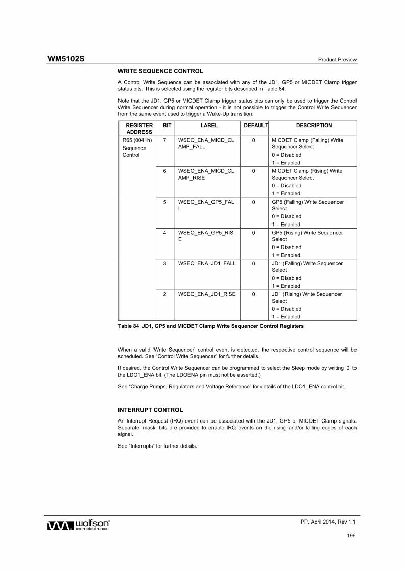
WM5102S Product Preview
w PP, April 2014, Rev 1.1
196
WRITE SEQUENCE CONTROL
A Control Write Sequence can be associated with any of the JD1, GP5 or MICDET Clamp trigger status bits. This is selected using the register bits described in Table 84.
Note that the JD1, GP5 or MICDET Clamp trigger status bits can only be used to trigger the Control Write Sequencer during normal operation - it is not possible to trigger the Control Write Sequencer from the same event used to trigger a Wake-Up transition.
REGISTER ADDRESS
BIT LABEL DEFAULT DESCRIPTION
R65 (0041h)
Sequence Control
7 WSEQ_ENA_MICD_CLAMP_FALL
0 MICDET Clamp (Falling) Write Sequencer Select
0 = Disabled
1 = Enabled
6 WSEQ_ENA_MICD_CLAMP_RISE
0 MICDET Clamp (Rising) Write Sequencer Select
0 = Disabled
1 = Enabled
5 WSEQ_ENA_GP5_FALL
0 GP5 (Falling) Write Sequencer Select
0 = Disabled
1 = Enabled
4 WSEQ_ENA_GP5_RISE
0 GP5 (Rising) Write Sequencer Select
0 = Disabled
1 = Enabled
3 WSEQ_ENA_JD1_FALL 0 JD1 (Falling) Write Sequencer Select
0 = Disabled
1 = Enabled
2 WSEQ_ENA_JD1_RISE 0 JD1 (Rising) Write Sequencer Select
0 = Disabled
1 = Enabled
Table 84 JD1, GP5 and MICDET Clamp Write Sequencer Control Registers
When a valid ‘Write Sequencer’ control event is detected, the respective control sequence will be scheduled. See “Control Write Sequencer” for further details.
If desired, the Control Write Sequencer can be programmed to select the Sleep mode by writing ‘0’ to the LDO1_ENA bit. (The LDOENA pin must not be asserted.)
See “Charge Pumps, Regulators and Voltage Reference” for details of the LDO1_ENA control bit.
INTERRUPT CONTROL
An Interrupt Request (IRQ) event can be associated with the JD1, GP5 or MICDET Clamp signals. Separate ‘mask’ bits are provided to enable IRQ events on the rising and/or falling edges of each signal.
See “Interrupts” for further details.
Product Preview WM5102S
w PP, April 2014, Rev 1.1
197
GENERAL PURPOSE INPUT / OUTPUT
The WM5102S provides a number of GPIO functions to enable interfacing and detection of external hardware and to provide logic outputs to other devices. The GPIO input functions can be used to generate an Interrupt (IRQ) event. The GPIO and Interrupt circuits support the following functions:
Digital audio interface function (AIFnTXLRCLK)
Logic input / Button detect (GPIO input)
Logic ‘1’ and logic ‘0’ output (GPIO output)
Interrupt (IRQ) status output
DSP Status Flag (DSP IRQn) and RAM status output
Clock output
Frequency Locked Loop (FLL) status output
Frequency Locked Loop (FLL) Clock output
Pulse Width Modulation (PWM) Signal output
Headphone Detection status output
Microphone / Accessory Detection status output
Asynchronous Sample Rate Converter (ASRC) Lock status and Configuration Error output
Control Write Sequencer status output
Over-Temperature status output
Dynamic Range Control (DRC) status output
Control Interface Error status output
Clocking Error status output
Digital audio interface Configuration Error status output
Note that the GPIO pins are referenced to different power domains (DBVDD1, DBVDD2 or DBVDD3), as noted in the “Pin Description” section.
In addition to the functions described in this section, the GPIO5 pin can be configured as an input to the Control Write Sequencer (see “Control Write Sequencer”). See also Table 84 for details of the associated register control fields.
The GPIO5 pin is one of the ‘Always On’ digital input / output pins and can be used as a ‘Wake-Up’ input in the low-power ‘Sleep’ mode. The GPIO5 pin can also be used as an input to the MICDET Clamp function, supporting additional functionality relating to jack insertion or jack removal events See “Low Power Sleep Configuration” for further details.
WM5102S Product Preview
w PP, April 2014, Rev 1.1
198
GPIO CONTROL
For each GPIO, the selected function is determined by the GPn_FN field, where n identifies the GPIO pin (1, 2, 3, 4 or 5). The pin direction, set by GPn_DIR, must be set according to function selected by GPn_FN.
When a pin is configured as a GPIO input (GPn_DIR = 1, GPn_FN = 01h), the logic level at the pin can be read from the respective GPn_LVL bit. Note that GPn_LVL is not affected by the GPn_POL bit.
A de-bounce circuit can be enabled on any GPIO input, to avoid false event triggers. This is enabled on each pin by setting the respective GPn_DB bit. The de-bounce circuit uses the 32kHz clock, which must be enabled whenever input de-bounce functions are required. The de-bounce time is configurable using the GP_DBTIME register. See “Clocking and Sample Rates” for further details of the WM5102S clocking configuration.
Each of the GPIO pins is an input to the Interrupt control circuit and can be used to trigger an Interrupt event. An interrupt event is triggered on the rising and falling edges of the GPIO input. The associated interrupt bit is latched once set; it can be polled at any time or used to control the IRQ signal. See “Interrupts” for more details of the Interrupt event handling.
When a pin is configured as a GPIO input, internal pull-up and pull-down resistors may be enabled using the GPn_PU and GPn_PD fields; this allows greater flexibility to interface with different signals from other devices. (Note that, if the pin is configured as an output, or if GPn_PU and GPn_PD are both set for any GPIO pin, then the pull-up and pull-down will be disabled.)
When a pin is configured as a GPIO output (GPn_DIR = 0, GPn_FN = 01h), its level can be set to logic 0 or logic 1 using the GPn_LVL field. Note that the GPn_LVL registers are ‘write only’ when the respective GPIO pin is configured as an output.
When a pin is configured as an output (GPn_DIR = 0), the polarity can be inverted using the GPn_POL bit. When GPn_POL = 1, then the selected output function is inverted. In the case of Logic Level output (GPn_FN = 01h), the external output will be the opposite logic level to GPn_LVL when GPn_POL = 1.
A GPIO output can be either CMOS driven or Open Drain. This is selected on each pin using the respective GPn_OP_CFG bit.
The register fields that control the GPIO pins are described in Table 85.
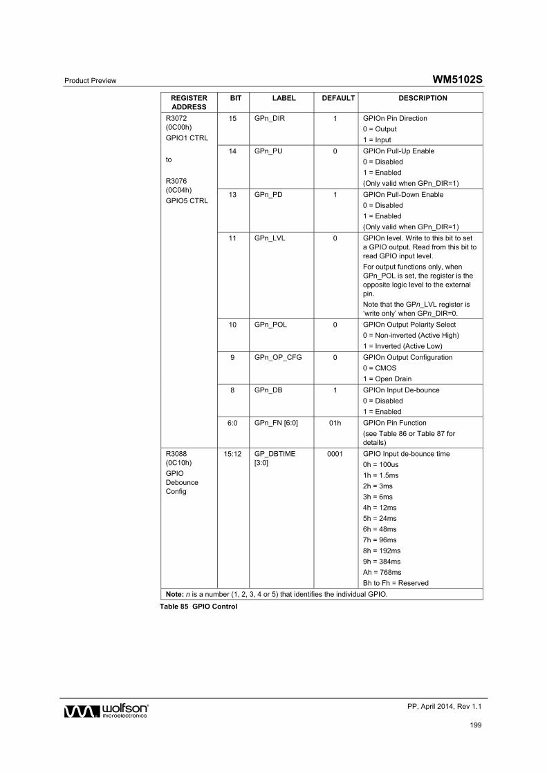
Product Preview WM5102S
w PP, April 2014, Rev 1.1
199
REGISTER ADDRESS
BIT LABEL DEFAULT DESCRIPTION
R3072 (0C00h)
GPIO1 CTRL
to
R3076 (0C04h)
GPIO5 CTRL
15 GPn_DIR 1 GPIOn Pin Direction
0 = Output
1 = Input
14 GPn_PU 0 GPIOn Pull-Up Enable
0 = Disabled
1 = Enabled
(Only valid when GPn_DIR=1)
13 GPn_PD 1 GPIOn Pull-Down Enable
0 = Disabled
1 = Enabled
(Only valid when GPn_DIR=1)
11 GPn_LVL 0 GPIOn level. Write to this bit to set a GPIO output. Read from this bit to read GPIO input level.
For output functions only, when GPn_POL is set, the register is the opposite logic level to the external pin.
Note that the GPn_LVL register is ‘write only’ when GPn_DIR=0.
10 GPn_POL 0 GPIOn Output Polarity Select
0 = Non-inverted (Active High)
1 = Inverted (Active Low)
9 GPn_OP_CFG 0 GPIOn Output Configuration
0 = CMOS
1 = Open Drain
8 GPn_DB 1 GPIOn Input De-bounce
0 = Disabled
1 = Enabled
6:0 GPn_FN [6:0] 01h GPIOn Pin Function
(see Table 86 or Table 87 for details)
R3088 (0C10h)
GPIO Debounce Config
15:12 GP_DBTIME [3:0]
0001 GPIO Input de-bounce time
0h = 100us
1h = 1.5ms
2h = 3ms
3h = 6ms
4h = 12ms
5h = 24ms
6h = 48ms
7h = 96ms
8h = 192ms
9h = 384ms
Ah = 768ms
Bh to Fh = Reserved
Note: n is a number (1, 2, 3, 4 or 5) that identifies the individual GPIO.
Table 85 GPIO Control
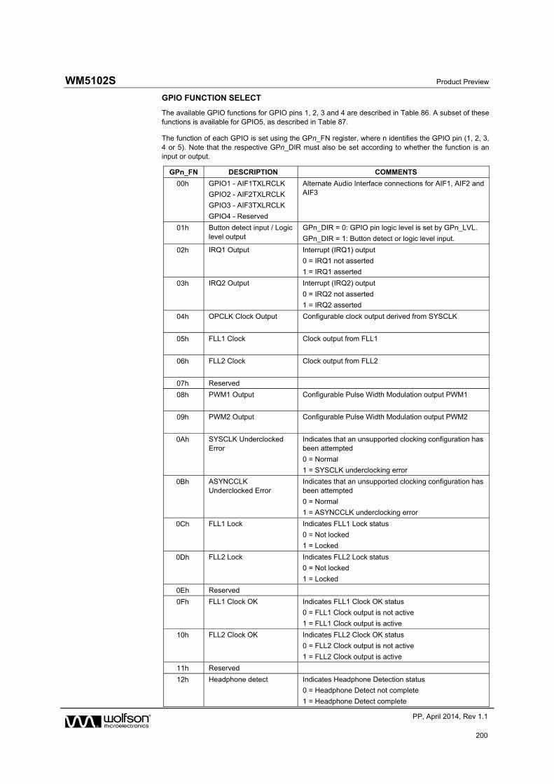
WM5102S Product Preview
w PP, April 2014, Rev 1.1
200
GPIO FUNCTION SELECT
The available GPIO functions for GPIO pins 1, 2, 3 and 4 are described in Table 86. A subset of these functions is available for GPIO5, as described in Table 87.
The function of each GPIO is set using the GPn_FN register, where n identifies the GPIO pin (1, 2, 3, 4 or 5). Note that the respective GPn_DIR must also be set according to whether the function is an input or output.
GPn_FN DESCRIPTION COMMENTS
00h GPIO1 - AIF1TXLRCLK
GPIO2 - AIF2TXLRCLK
GPIO3 - AIF3TXLRCLK
GPIO4 - Reserved
Alternate Audio Interface connections for AIF1, AIF2 and AIF3
01h Button detect input / Logic level output
GPn_DIR = 0: GPIO pin logic level is set by GPn_LVL.
GPn_DIR = 1: Button detect or logic level input.
02h IRQ1 Output Interrupt (IRQ1) output
0 = IRQ1 not asserted
1 = IRQ1 asserted
03h IRQ2 Output Interrupt (IRQ2) output
0 = IRQ2 not asserted
1 = IRQ2 asserted
04h OPCLK Clock Output Configurable clock output derived from SYSCLK
05h FLL1 Clock Clock output from FLL1
06h FLL2 Clock Clock output from FLL2
07h Reserved
08h PWM1 Output Configurable Pulse Width Modulation output PWM1
09h PWM2 Output Configurable Pulse Width Modulation output PWM2
0Ah SYSCLK Underclocked Error
Indicates that an unsupported clocking configuration has been attempted
0 = Normal
1 = SYSCLK underclocking error
0Bh ASYNCCLK Underclocked Error
Indicates that an unsupported clocking configuration has been attempted
0 = Normal
1 = ASYNCCLK underclocking error
0Ch FLL1 Lock Indicates FLL1 Lock status
0 = Not locked
1 = Locked
0Dh FLL2 Lock Indicates FLL2 Lock status
0 = Not locked
1 = Locked
0Eh Reserved
0Fh FLL1 Clock OK Indicates FLL1 Clock OK status
0 = FLL1 Clock output is not active
1 = FLL1 Clock output is active
10h FLL2 Clock OK Indicates FLL2 Clock OK status
0 = FLL2 Clock output is not active
1 = FLL2 Clock output is active
11h Reserved
12h Headphone detect Indicates Headphone Detection status
0 = Headphone Detect not complete
1 = Headphone Detect complete

Product Preview WM5102S
w PP, April 2014, Rev 1.1
201
GPn_FN DESCRIPTION COMMENTS
13h Microphone detect Microphone Detect (MICDET accessory) IRQ output
A single 31s pulse is output whenever an accessory insertion, removal or impedance change is detected.
14h Reserved
15h Write Sequencer status Indicates Write Sequencer status
A short pulse is output when the Write Sequencer has completed all scheduled sequences.
16h Control Interface Address Error
Indicates Control Interface Address error
0 = Normal
1 = Control Interface Address error
17h Reserved
18h Reserved
19h Reserved
1Ah ASRC1 Lock Indicates ASRC1 Lock status
0 = Not locked
1 = Locked
1Bh ASRC2 Lock Indicates ASRC2 Lock status
0 = Not locked
1 = Locked
1Ch ASRC Configuration Error Indicates ASRC configuration error
0 = ASRC configuration OK
1 = ASRC configuration error
1Dh DRC1 Signal Detect Indicates DRC1 Signal Detect status
0 = Signal threshold not exceeded
1 = Signal threshold exceeded
1Eh DRC1 Anti-Clip Active Indicates DRC1 Anti-Clip status
0 = Anti-Clip is not active
1 = Anti-Clip is active
1Fh DRC1 Decay Active Indicates DRC1 Decay status
0 = Decay is not active
1 = Decay is active
20h DRC1 Noise Gate Active Indicates DRC1 Noise Gate status
0 = Noise Gate is not active
1 = Noise Gate is active
21h DRC1 Quick Release Active
Indicates DRC1 Quick Release status
0 = Quick Release is not active
1 = Quick Release is active
22h Reserved
23h Reserved
24h Reserved
25h Reserved
26h Reserved
27h Mixer Dropped Sample Error
Indicates a dropped sample in the digital core mixers
0 = Normal
1 = Mixer dropped sample error
28h AIF1 Configuration Error Indicates AIF1 configuration error
0 = AIF1 configuration OK
1 = AIF1 configuration error
29h AIF2 Configuration Error Indicates AIF2 configuration error
0 = AIF2 configuration OK
1 = AIF2 configuration error
2Ah AIF3 Configuration Error Indicates AIF3 configuration error
0 = AIF3 configuration OK
1 = AIF3 configuration error
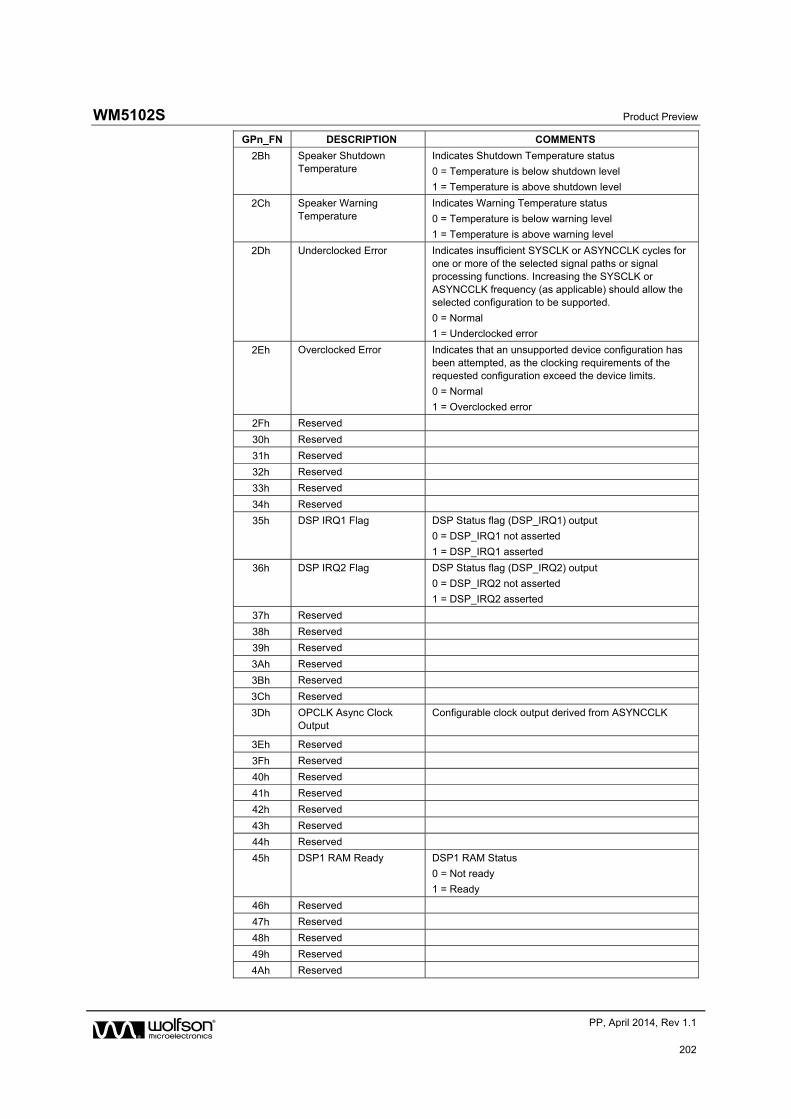
WM5102S Product Preview
w PP, April 2014, Rev 1.1
202
GPn_FN DESCRIPTION COMMENTS
2Bh Speaker Shutdown Temperature
Indicates Shutdown Temperature status
0 = Temperature is below shutdown level
1 = Temperature is above shutdown level
2Ch Speaker Warning Temperature
Indicates Warning Temperature status
0 = Temperature is below warning level
1 = Temperature is above warning level
2Dh Underclocked Error Indicates insufficient SYSCLK or ASYNCCLK cycles for one or more of the selected signal paths or signal processing functions. Increasing the SYSCLK or ASYNCCLK frequency (as applicable) should allow the selected configuration to be supported.
0 = Normal
1 = Underclocked error
2Eh Overclocked Error Indicates that an unsupported device configuration has been attempted, as the clocking requirements of the requested configuration exceed the device limits.
0 = Normal
1 = Overclocked error
2Fh Reserved
30h Reserved
31h Reserved
32h Reserved
33h Reserved
34h Reserved
35h DSP IRQ1 Flag DSP Status flag (DSP_IRQ1) output
0 = DSP_IRQ1 not asserted
1 = DSP_IRQ1 asserted
36h DSP IRQ2 Flag DSP Status flag (DSP_IRQ2) output
0 = DSP_IRQ2 not asserted
1 = DSP_IRQ2 asserted
37h Reserved
38h Reserved
39h Reserved
3Ah Reserved
3Bh Reserved
3Ch Reserved
3Dh OPCLK Async Clock Output
Configurable clock output derived from ASYNCCLK
3Eh Reserved
3Fh Reserved
40h Reserved
41h Reserved
42h Reserved
43h Reserved
44h Reserved
45h DSP1 RAM Ready DSP1 RAM Status
0 = Not ready
1 = Ready
46h Reserved
47h Reserved
48h Reserved
49h Reserved
4Ah Reserved
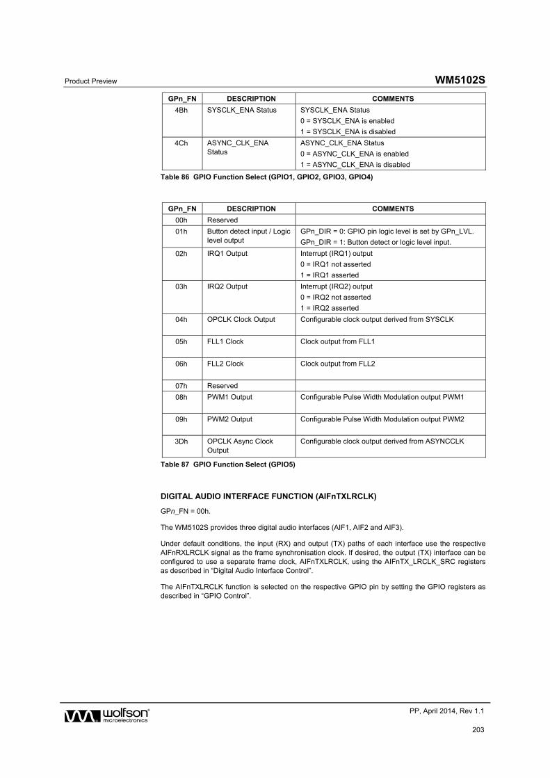
Product Preview WM5102S
w PP, April 2014, Rev 1.1
203
GPn_FN DESCRIPTION COMMENTS
4Bh SYSCLK_ENA Status SYSCLK_ENA Status
0 = SYSCLK_ENA is enabled
1 = SYSCLK_ENA is disabled
4Ch ASYNC_CLK_ENA Status
ASYNC_CLK_ENA Status
0 = ASYNC_CLK_ENA is enabled
1 = ASYNC_CLK_ENA is disabled
Table 86 GPIO Function Select (GPIO1, GPIO2, GPIO3, GPIO4)
GPn_FN DESCRIPTION COMMENTS
00h Reserved
01h Button detect input / Logic level output
GPn_DIR = 0: GPIO pin logic level is set by GPn_LVL.
GPn_DIR = 1: Button detect or logic level input.
02h IRQ1 Output Interrupt (IRQ1) output
0 = IRQ1 not asserted
1 = IRQ1 asserted
03h IRQ2 Output Interrupt (IRQ2) output
0 = IRQ2 not asserted
1 = IRQ2 asserted
04h OPCLK Clock Output Configurable clock output derived from SYSCLK
05h FLL1 Clock Clock output from FLL1
06h FLL2 Clock Clock output from FLL2
07h Reserved
08h PWM1 Output Configurable Pulse Width Modulation output PWM1
09h PWM2 Output Configurable Pulse Width Modulation output PWM2
3Dh OPCLK Async Clock Output
Configurable clock output derived from ASYNCCLK
Table 87 GPIO Function Select (GPIO5)
DIGITAL AUDIO INTERFACE FUNCTION (AIFnTXLRCLK)
GPn_FN = 00h.
The WM5102S provides three digital audio interfaces (AIF1, AIF2 and AIF3).
Under default conditions, the input (RX) and output (TX) paths of each interface use the respective AIFnRXLRCLK signal as the frame synchronisation clock. If desired, the output (TX) interface can be configured to use a separate frame clock, AIFnTXLRCLK, using the AIFnTX_LRCLK_SRC registers as described in “Digital Audio Interface Control”.
The AIFnTXLRCLK function is selected on the respective GPIO pin by setting the GPIO registers as described in “GPIO Control”.
WM5102S Product Preview
w PP, April 2014, Rev 1.1
204
BUTTON DETECT (GPIO INPUT)
GPn_FN = 01h.
Button detect functionality can be selected on any GPIO pin by setting the respective GPIO registers as described in “GPIO Control”. The same functionality can be used to support a Jack Detect input function.
It is recommended to enable the GPIO input de-bounce feature when using GPIOs as button input or Jack Detect input.
The GPn_LVL fields may be read to determine the logic levels on a GPIO input, after the selectable de-bounce controls. Note that GPn_LVL is not affected by the GPn_POL bit.
The de-bounced GPIO signals are also inputs to the Interrupt control circuit. An interrupt event is triggered on the rising and falling edges of the GPIO input. The associated interrupt bits are latched once set; it can be polled at any time or used to control the IRQ signal. See “Interrupts” for more details of the Interrupt event handling.
LOGIC ‘1’ AND LOGIC ‘0’ OUTPUT (GPIO OUTPUT)
GPn_FN = 01h.
The WM5102S can be programmed to drive a logic high or logic low level on any GPIO pin by selecting the “GPIO Output” function as described in “GPIO Control”.
The output logic level is selected using the respective GPn_LVL bit. Note that the GPn_LVL registers are ‘write only’ when the respective GPIO pin is configured as an output.
The polarity of the GPIO output can be inverted using the GPn_POL registers. If GPn_POL=1, then the external output will be the opposite logic level to GPn_LVL.
INTERRUPT (IRQ) STATUS OUTPUT
GPn_FN = 02h, 03h.
The WM5102S has an Interrupt Controller which can be used to indicate when any selected Interrupt events occur. An interrupt can be generated by any of the events described throughout the GPIO function definition above. Individual interrupts may be masked in order to configure the Interrupt as required. See “Interrupts” for further details.
The Interrupt Controller supports two separate Interrupt Request (IRQ) outputs. The IRQ1 or IRQ2 status may be output directly on any GPIO pin by setting the respective GPIO registers as described in “GPIO Control”.
Note that the IRQ1 status is output on the IRQ¯¯¯ pin at all times.
Product Preview WM5102S
w PP, April 2014, Rev 1.1
205
DSP STATUS FLAG (DSP IRQn) OUTPUT
GPn_FN = 35h, 36h, 45h.
The WM5102S supports two DSP Status flags as outputs from the DSP block. These are configurable within the DSP to provide external indication of the required function(s). A status flag indicating the DSP1 RAM status is also supported. See “Digital Core” for more details of the DSP.
The DSP Status and DSP RAM Ready flags may be output directly on any GPIO pin by setting the respective GPIO registers as described in “GPIO Control”. The DSP Status and DSP RAM Ready outputs are described in Table 88.
The DSP Status flags are inputs to the Interrupt Controller circuit. An interrupt event is triggered on the rising edge of the DSP Status (DSP_IRQn) flags or DSP RAM Ready flags. The associated interrupt bits are latched once set; they can be polled at any time or used to control the IRQ signal. See “Interrupts” for more details of the Interrupt event handling.
GPN_FN DESCRIPTION COMMENTS
35h DSP Status (DSP_IRQ1) External indication of DSP_IRQ1_STS
36h DSP Status (DSP_IRQ2) External indication of DSP_IRQ2_STS
45h DSP1 RAM Ready Indicates DSP1 RAM Ready status
Table 88 DSP Status and RAM Ready Indications
OPCLK AND OPCLK_ASYNC CLOCK OUTPUT
GPn_FN = 04h, 3Dh.
A clock output (OPCLK) derived from SYSCLK can be output on any GPIO pin. The OPCLK frequency is controlled by OPCLK_DIV and OPCLK_SEL. The OPCLK output is enabled using the OPCLK_ENA register, as described in Table 89.
A clock output (OPCLK_ASYNC) derived from ASYNCCLK can be output on any GPIO pin. The OPCLK_ASYNC frequency is controlled by OPCLK_ASYNC_DIV and OPCLK_ASYNC_SEL. The OPCLK_ASYNC output is enabled using the OPCLK_ASYNC_ENA register
It is recommended to disable the clock output (OPCLK_ENA=0 or OPCLK_ASYNC_ENA=0) before making any change to the respective OPCLK_DIV, OPCLK_SEL, OPCLK_ASYNC_DIV or OPCLK_ASYNC_SEL registers.
The OPCLK or OPCLK_ASYNC Clock outputs can be output directly on any GPIO pin by setting the respective GPIO registers as described in “GPIO Control”.
Note that the OPCLK source frequency cannot be higher than the SYSCLK frequency. The OPCLK_ASYNC source frequency cannot be higher than the ASYNCCLK frequency. The maximum output frequency supported for GPIO output is noted in the “Electrical Characteristics”.
See “Clocking and Sample Rates” for more details of the system clocks (SYSCLK and ASYNCCLK).
REGISTER ADDRESS
BIT LABEL DEFAULT DESCRIPTION
R329 (0149h)
Output system clock
15 OPCLK_ENA 0 OPCLK Enable
0 = Disabled
1 = Enabled
7:3 OPCLK_DIV [4:0] 00h OPCLK Divider
00h = Divide by 1
01h = Divide by 1
02h = Divide by 2
03h = Divide by 3
…
1Fh = Divide by 31
WM5102S Product Preview
w PP, April 2014, Rev 1.1
206
REGISTER ADDRESS
BIT LABEL DEFAULT DESCRIPTION
2:0 OPCLK_SEL [2:0] 000 OPCLK Source Frequency
000 = 6.144MHz (5.6448MHz)
001 = 12.288MHz (11.2896MHz)
010 = 24.576MHz (22.5792MHz)
011 = 49.152MHz (45.1584MHz)
All other codes are Reserved
The frequencies in brackets apply for 44.1kHz-related SYSCLK rates only (ie. SAMPLE_RATE_n = 01XXX).
The OPCLK Source Frequency must be less than or equal to the SYSCLK frequency.
R330 (014Ah)
Output async clock
15 OPCLK_ASYNC_ENA
0 OPCLK_ASYNC Enable
0 = Disabled
1 = Enabled
7:3 OPCLK_ASYNC_DIV [4:0]
00h OPCLK_ASYNC Divider
00h = Divide by 1
01h = Divide by 1
02h = Divide by 2
03h = Divide by 3
…
1Fh = Divide by 31
2:0 OPCLK_ASYNC_SEL [2:0]
000 OPCLK_ASYNC Source Frequency
000 = 6.144MHz (5.6448MHz)
001 = 12.288MHz (11.2896MHz)
010 = 24.576MHz (22.5792MHz)
011 = 49.152MHz (45.1584MHz)
All other codes are Reserved
The frequencies in brackets apply for 44.1kHz-related ASYNCCLK rates only (ie. ASYNC_SAMPLE_RATE_n = 01XXX).
The OPCLK_ASYNC Source Frequency must be less than or equal to the ASYNCCLK frequency.
Table 89 OPCLK and OPCLK_ASYNC Control
FREQUENCY LOCKED LOOP (FLL) STATUS OUTPUT
GPn_FN = 0Ch, 0Dh, 0Fh, 10h.
The WM5102S supports FLL status flags, which may be used to control other events. See “Clocking and Sample Rates” for more details of the FLL.
The ‘FLL Clock OK’ signals indicate that the respective FLL has started up and is providing an output clock. The ‘FLL Lock’ signals indicate whether FLL Lock has been achieved.
The FLL Clock OK and FLL Lock signals may be output directly on any GPIO pin by setting the respective GPIO registers as described in “GPIO Control”.
The FLL Clock OK and FLL Lock signals are inputs to the Interrupt Controller circuit. An interrupt event is triggered on the rising and falling edges of these signals. The associated interrupt bits are latched once set; they can be polled at any time or used to control the IRQ signal. See “Interrupts” for more details of the Interrupt event handling.
Product Preview WM5102S
w PP, April 2014, Rev 1.1
207
FREQUENCY LOCKED LOOP (FLL) CLOCK OUTPUT
GPn_FN = 05h, 06h.
Clock outputs derived from the FLLs may be output on any GPIO pin. The GPIO output from each FLLn (where ‘n’ is 1 or 2) is controlled by the respective FLLn_GPCLK_DIV and FLLn_GPCLK_ENA registers, as described in Table 90.
It is recommended to disable the clock output (FLLn_GPCLK_ENA=0) before making any change to the respective FLLn_GPCLK_DIV register.
Note that the FLLn_GPCLK_DIV and FLLn_GPCLK_ENA registers affect the GPIO outputs only; they do not affect the FLL frequency. The maximum output frequency supported for GPIO output is noted in the “Electrical Characteristics”.
The Frequency Locked Loop (FLL) Clock outputs may be output directly on any GPIO pin by setting the respective GPIO registers as described in “GPIO Control”.
See “Clocking and Sample Rates” for more details of the WM5102S system clocking and for details of how to configure the FLLs.
REGISTER ADDRESS
BIT LABEL DEFAULT DESCRIPTION
R394 (018Ah)
FLL1 GPIO Clock
7:1 FLL1_GPCLK_DIV [6:0]
02h FLL1 GPIO Clock Divider
00h = Divide by 1
01h = Divide by 1
02h = Divide by 2
03h = Divide by 3
…
7Fh = Divide by 127
(FGPIO = FVCO / FLL1_GPCLK_DIV)
0 FLL1_GPCLK_ENA
0 FLL1 GPIO Clock Enable
0 = Disabled
1 = Enabled
R426 (01AAh)
FLL2 GPIO Clock
7:1 FLL2_GPCLK_DIV [6:0]
02h FLL2 GPIO Clock Divider
00h = Divide by 1
01h = Divide by 1
02h = Divide by 2
03h = Divide by 3
…
7Fh = Divide by 127
(FGPIO = FVCO / FLL2_GPCLK_DIV)
0 FLL2_GPCLK_ENA
0 FLL2 GPIO Clock Enable
0 = Disabled
1 = Enabled
Table 90 FLL Clock Output Control
PULSE WIDTH MODULATION (PWM) SIGNAL OUTPUT
GPn_FN = 08h, 09h.
The WM5102S incorporates two Pulse Width Modulation (PWM) signal generators which can be enabled as GPIO outputs. The duty cycle of each PWM signal can be modulated by an audio source, or can be set to a fixed value using a control register setting.
The Pulse Width Modulation (PWM) outputs may be output directly on any GPIO pin by setting the respective GPIO registers as described in “GPIO Control”.
See “Digital Core” for details of how to configure the PWM signal generators.
WM5102S Product Preview
w PP, April 2014, Rev 1.1
208
HEADPHONE DETECTION STATUS OUTPUT
GPn_FN = 12h.
The WM5102S provides a headphone detection circuit on the HPDETL and HPDETR pins to measure the impedance of an external load connected to the headphone outputs. See “External Accessory Detection” for further details.
A logic signal from the headphone detection circuit may be output directly on any GPIO pin by setting the respective GPIO registers as described in “GPIO Control”. This logic signal is set low when a Headphone Detect measurement is triggered, and is set high when the Headphone Detect function has completed. A rising edge indicates completion of a Headphone Detect measurement.
The headphone detection circuit is also an input to the Interrupt control circuit. An interrupt event is triggered whenever a headphone detection measurement has completed. Note that the HPDET_EINT flag is also asserted when the headphone detection is initiated. The associated interrupt bit is latched once set; it can be polled at any time or used to control the IRQ signal. See “Interrupts” for more details of the Interrupt event handling.
MICROPHONE / ACCESSORY DETECTION STATUS OUTPUT
GPn_FN = 13h.
The WM5102S provides an impedance measurement circuit on the MICDETn pins to detect the connection of a microphone or other external accessory. See “External Accessory Detection” for further details.
A logic signal from the microphone detect circuit may be output directly on any GPIO pin by setting the respective GPIO registers as described in “GPIO Control”. This logic signal is set high for a pulse duration of 31s whenever an accessory insertion, removal or impedance change is detected.
The microphone detection circuit is also an input to the Interrupt control circuit. An interrupt event is triggered whenever an accessory insertion, removal or impedance change is detected. The associated interrupt bit is latched once set; it can be polled at any time or used to control the IRQ signal. See “Interrupts” for more details of the Interrupt event handling.
ASYNCHRONOUS SAMPLE RATE CONVERTER (ASRC) LOCK STATUS OUTPUT
GPn_FN = 1Ah, 1Bh.
The WM5102S maintains a flag indicating the lock status of the Asynchronous Sample Rate Converters (ASRCs), which may be used to control other events if required. See “Digital Core” for more details of the ASRCs.
The ASRC Lock signals may be output directly on any GPIO pin by setting the respective GPIO registers as described in “GPIO Control”.
The ASRC Lock signals are inputs to the Interrupt control circuit. An interrupt event is triggered on the rising and falling edges of the ASRC Lock signals. The associated interrupt bits are latched once set; they can be polled at any time or used to control the IRQ signal. See “Interrupts” for more details of the Interrupt event handling.
Product Preview WM5102S
w PP, April 2014, Rev 1.1
209
ASYNCHRONOUS SAMPLE RATE CONVERTER (ASRC) CONFIGURATION ERROR STATUS OUTPUT
GPn_FN = 1Ch.
The WM5102S performs automatic checks to confirm that the ASRCs are configured with valid settings. Invalid settings include conditions where one of the associated sample rates is higher than 48kHz. If an invalid ASRC configuration is detected, this can be indicated using the GPIO and/or Interrupt functions.
The ASRC Configuration Error signal may be output directly on any GPIO pin by setting the respective GPIO registers as described in “GPIO Control”.
The ASRC Configuration Error signal is an input to the Interrupt Controller circuit. An interrupt event is triggered on the rising and falling edges of the ASRC Configuration Error signal. The associated interrupt bit is latched once set; it can be polled at any time or used to control the IRQ signal. See “Interrupts” for more details of the Interrupt event handling.
OVER-TEMPERATURE STATUS OUTPUT
GPn_FN = 2Bh, 2Ch.
The WM5102S incorporates a temperature sensor which detects when the device temperature is within normal limits or if the device is approaching a hazardous temperature condition.
The temperature status may be output directly on any GPIO pin by setting the respective GPIO registers as described in “GPIO Control”. Any GPIO pin can be used to indicate either a Warning Temperature event or the Shutdown Temperature event.
The Warning Temperature and Shutdown Temperature status are inputs to the Interrupt control circuit. An interrupt event may be triggered on the rising and falling edges of these signals. The associated interrupt bit is latched once set; it can be polled at any time or used to control the IRQ signal. See “Interrupts” for more details of the Interrupt event handling.
It is strongly recommended that the speaker drivers be disabled if the Shutdown Temperature condition occurs.
DYNAMIC RANGE CONTROL (DRC) STATUS OUTPUT
GPn_FN = 1Dh, 1Eh, 1Fh, 20h, 21h.
The Dynamic Range Control (DRC) circuit provides status outputs, which may be used to control other events if required.
The DRC status flags may be output directly on any GPIO pin by setting the respective GPIO registers as described in “GPIO Control”. The DRC status outputs are described in Table 91.
See “Digital Core” for more details of the DRC.
GPN_FN DESCRIPTION COMMENTS
1Dh DRC1 Signal Detect Indicates a signal is present on the respective DRC path. The threshold level is configurable (see Table 14).
1Eh DRC1 Anti-Clip Active Indicates the DRC anti-clip function has been triggered; the DRC gain is decreasing in response to a rising signal level.
1Fh DRC1 Decay Active Indicates that the DRC gain is increasing in response to a low-level signal input.
20h DRC1 Noise Gate Active Indicates that the DRC noise gate has been triggered; an idle signal condition has been detected.
21h DRC1 Quick Release Active
Indicates that the DRC quick-release function has been triggered; the DRC gain is increasing rapidly following detection of a short transient peak.
Table 91 Dynamic Range Control (DRC) Status Indications
WM5102S Product Preview
w PP, April 2014, Rev 1.1
210
CONTROL WRITE SEQUENCER STATUS OUTPUT
GPn_FN = 15h.
The WM5102S Control Write Sequencer (WSEQ) can be used to execute a sequence of register write operations in response to a simple trigger event. See “Control Write Sequencer” for details of the Control Write Sequencer.
The WSEQ_BUSY register bit (see Table 116) indicates the status of the Control Write Sequencer. When WSEQ_BUSY=1, this indicates that one or more Write Sequence operations are in progress or are queued for sequential execution.
A logic signal from the Write Sequencer function may be output directly on any GPIO pin by setting the respective GPIO registers as described in “GPIO Control”. This logic signal is set high for a short pulse duration (approx. 100ns) whenever the Write Sequencer has completed all scheduled sequences, and there are no more pending operations.
The Write Sequencer status is an input to the Interrupt control circuit. An interrupt event is triggered on completion of a Control Sequence. The associated interrupt bit is latched once set; it can be polled at any time or used to control the IRQ signal. See “Interrupts” for more details of the Interrupt event handling.
CONTROL INTERFACE ERROR STATUS OUTPUT
GPn_FN = 16h.
The WM5102S is controlled by writing to registers through a 2-wire (I2C) or 4-wire (SPI) serial control interface, as described in the “Control Interface” section. The SLIMbus interface also supports read/write access to the control registers, as described in the “SLIMbus Interface Control” section.
The WM5102S performs automatic checks to confirm if a register access is successful. Register access will be unsuccessful if an invalid register address is selected. Read/write access to the DSP firmware memory will be unsuccessful if the associated clocking is not enabled. If an invalid or unsuccessful register operation is attempted, this can be indicated using the GPIO and/or Interrupt functions.
The Control Interface Error signal may be output directly on any GPIO pin by setting the respective GPIO registers as described in “GPIO Control”.
The Control Interface Error signal is an input to the Interrupt Controller circuit. An interrupt event is triggered on the rising edge of the Control Interface Error signal. The associated interrupt bit is latched once set; it can be polled at any time or used to control the IRQ signal. See “Interrupts” for more details of the Interrupt event handling.
SYSTEM CLOCKS ENABLE STATUS OUTPUT
GPn_FN = 4Bh, 4Ch.
The WM5102S requires a system clock (SYSCLK) for its internal functions and to support the input/output signal paths. The WM5102S can support two independent clock domains, with selected functions referenced to the ASYNCCLK clock domain. See “Clocking and Sample Rates” for details of these clocks.
The SYSCLK_ENA and ASYNC_CLK_ENA registers (see Table 100) control the SYSCLK and ASYNCCLK signals respectively. When ‘0’ is written to these registers, the host processor must wait until the WM5102S has shut down the associated functions before issuing any other register write commands.
The SYSCLK Enable and ASYNCCLK Enable status may be output directly on any GPIO pin by setting the respective GPIO registers as described in “GPIO Control”.
The SYSCLK Enable and ASYNCCLK Enable signals are inputs to the Interrupt Controller circuit. An interrupt event is triggered when the respective clock functions have been shut down. The associated interrupt bit is latched once set; it can be polled at any time or used to control the IRQ signal. See “Interrupts” for more details of the Interrupt event handling.
Product Preview WM5102S
w PP, April 2014, Rev 1.1
211
CLOCKING ERROR STATUS OUTPUT
GPn_FN = 0Ah, 0Bh, 27h, 2Dh, 2Eh.
The WM5102S performs automatic checks to confirm that the system clocks are correctly configured according to the commanded functionality. An invalid configuration is one where there are insufficient clock cycles to support the digital processing required by the commanded signal paths.
An Underclocked Error condition is where there are insufficient clock cycles for the requested functionality, and increasing the SYSCLK or ASYNCCLK frequency (as applicable) should allow the selected configuration to be supported.
An Overclocked Error condition is where the requested functionality cannot be supported, as the clocking requirements of the requested configuration exceed the device limits.
The system clocks (SYSCLK and, where applicable, ASYNCCLK) must be enabled before any signal path is enabled. If an attempt is made to enable a signal path, and there are insufficient clock cycles to support that path, then the attempt will be unsuccessful. Note that any signal paths that are already active will not be affected under these circumstances.
The Clocking Error signals may be output directly on any GPIO pin by setting the respective GPIO registers as described in “GPIO Control”. The Clocking Error conditions are described in Table 92.
The Clocking Error signals are inputs to the Interrupt Controller circuit. An interrupt event is triggered on the rising and falling edges of the Clocking Error signals. The associated interrupt bits are latched once set; they can be polled at any time or used to control the IRQ signal. See “Interrupts” for more details of the Interrupt event handling.
GPN_FN DESCRIPTION COMMENTS
0Ah SYSCLK Underclocked Indicates insufficient SYSCLK cycles for the commanded functionality.
0Bh ASYNCCLK Underclocked
Indicates insufficient ASYNCCLK cycles for the commanded functionality.
27h Mixer Dropped Sample Error
Indicates a dropped sample in the digital core mixer function.
2Dh Underclocked Error Indicates insufficient SYSCLK or ASYNCCLK cycles for one or more of the selected signal paths or signal processing functions. Increasing the SYSCLK or ASYNCCLK frequency (as applicable) should allow the selected configuration to be supported.
Status bits associated with specific sub-systems provide further de-bug capability.
The INnx_ENA_STS bits in register R769 indicate the status of each of the input (analogue or digital microphone) signal paths.
The OUTnx_ENA_STS bits in registers R1025 and R1030 indicate the status of each of the output (Headphone, Speaker or PDM) signal paths.
The ASRCnx_ENA_STS bits in register R3809 indicate the status of each of the ASRC signal paths.
The FX_STS field in register R3585 indicates the status of each of the Effects (EQ, DRC or LHPF) signal paths.
The *MIX_STSn fields in registers R1600 to R2920 indicate the status of each of the Digital Core mixer signal paths.
The ISRCn and AIFn functions are also inputs to the Underclocked Error status indication, but there are no specific _STS register bits associated with these.
2Eh Overclocked Error Indicates that an unsupported device configuration has been attempted, as the clocking requirements of the requested configuration exceed the device limits.
Table 92 Clocking Error Status Indications
WM5102S Product Preview
w PP, April 2014, Rev 1.1
212
DIGITAL AUDIO INTERFACE CONFIGURATION ERROR STATUS OUTPUT
GPn_FN = 28h, 29h, 2Ah.
The WM5102S performs automatic checks to confirm that AIF1, AIF2 and AIF3 are configured with valid settings. Invalid settings include conditions where one or more audio channel timeslots are in conflict.
If an invalid AIF1, AIF2 or AIF3 configuration is detected, this can be indicated using the GPIO and/or Interrupt functions.
The AIF Configuration Error signals may be output directly on any GPIO pin by setting the respective GPIO registers as described in “GPIO Control”.
The AIF Configuration Error signals are an input to the Interrupt Controller circuit. An interrupt event is triggered on the rising and falling edges of the AIF Configuration Error signal. The associated interrupt bit is latched once set; it can be polled at any time or used to control the IRQ signal. See “Interrupts” for more details of the Interrupt event handling.

Product Preview WM5102S
w PP, April 2014, Rev 1.1
213
INTERRUPTS
The Interrupt Controller has multiple inputs. These include the Jack Detect and GPIO input pins, DSP_IRQn flags, headphone / accessory detection, FLL / ASRC Lock detection, and Clocking configuration error indications. Any combination of these inputs can be used to trigger an Interrupt Request (IRQ) event.
The Interrupt Controller supports two sets of interrupt registers. This allows two separate Interrupt Request (IRQ) outputs to be generated, and for each IRQ to report a different set of input or status conditions.
For each Interrupt Request (IRQ1 and IRQ2) output, there is an Interrupt register field associated with each of the interrupt inputs. These fields are asserted whenever a logic edge is detected on the respective input. Some inputs are triggered on rising edges only; some are triggered on both edges. Separate rising and falling interrupt registers are provided for the JD1 and GP5 signals. The Interrupt register fields for IRQ1 are described in Table 94. The Interrupt register fields for IRQ2 are described in Table 95. The Interrupt flags can be polled at any time, or else in response to the Interrupt Request (IRQ) output being signalled via the IRQ¯¯¯ pin or a GPIO pin.
All of the Interrupts are edge-triggered, as noted above. Many of these are triggered on both the rising and falling edges and, therefore, the Interrupt registers cannot indicate which edge has been detected. The “Raw Status” fields described in Table 96 provide readback of the current value of the corresponding inputs to the Interrupt Controller. Note that the status of any GPIO inputs can be read using the GPn_LVL registers, as described in Table 85.
The UNDERCLOCKED_STS and OVERCLOCKED_STS registers represent the logical ‘OR’ of status flags from multiple sub-systems. The status bits in registers R3364 to R3366 (see Table 96) provide readback of these lower-level signals. See “Clocking and Sample Rates” for a description of the Underclocked and Overclocked Error conditions.
Individual mask bits can enable or disable different functions from the Interrupt controller. The mask bits are described in Table 94 (for IRQ1) and Table 95 (for IRQ2). Note that a masked interrupt input will not assert the corresponding interrupt register field, and will not cause the associated Interrupt Request (IRQ) output to be asserted.
The Interrupt Request (IRQ) outputs represent the logical ‘OR’ of the associated interrupt registers. (IRQ1 is derived from the _EINT1 registers; IRQ2 is derived from the _EINT2 registers). The Interrupt register fields are latching fields and, once they are set, they are not reset until a ‘1’ is written to the respective register bit(s). The Interrupt Request (IRQ) outputs are not reset until each of the associated interrupts has been reset.
A de-bounce circuit can be enabled on any GPIO input, to avoid false event triggers. This is enabled on each pin using the register bits described in Table 85.
The IRQ outputs can be globally masked using the IM_IRQ1 and IM_IRQ2 register bits. When not masked, the IRQ status can be read from IRQ1_STS and IRQ2_STS for the respective IRQ outputs.
The IRQ1 output is provided externally on the IRQ¯¯¯ pin. Under default conditions, this output is ‘Active Low’. The polarity can be inverted using the IRQ_POL register. The IRQ¯¯¯ output can be either CMOS driven or Open Drain; this is selected using the IRQ_OP_CFG register.
The IRQ1 and IRQ2 signals may be output on a GPIO pin - see “General Purpose Input / Output”.
The WM5102S Interrupt Controller circuit is illustrated in Figure 67. (Note that not all interrupt inputs are shown.) The associated control fields are described in Table 93 to Table 96.
Note that, under default register conditions, the ‘Boot Done’ status is the only un-masked interrupt source; a falling edge on the IRQ¯¯¯ pin will indicate completion of the Boot Sequence.

WM5102S Product Preview
w PP, April 2014, Rev 1.1
214
Figure 67 Interrupt Controller
REGISTER ADDRESS
BIT LABEL DEFAULT DESCRIPTION
R3087 (0C0Fh)
IRQ CTRL 1
10 IRQ_POL 1 IRQ Output Polarity Select
0 = Non-inverted (Active High)
1 = Inverted (Active Low)
9 IRQ_OP_CFG 0 IRQ Output Configuration
0 = CMOS
1 = Open Drain
Table 93 IRQ Output Control Registers
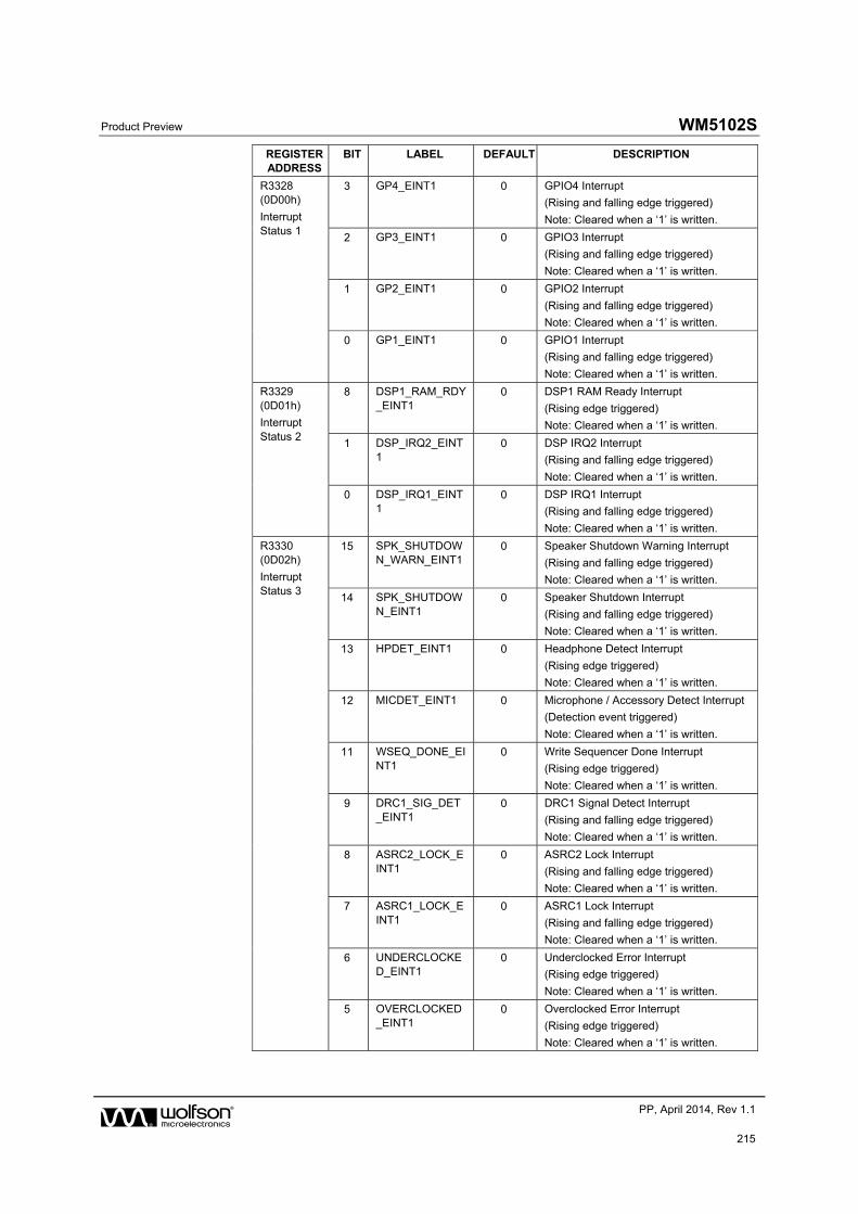
Product Preview WM5102S
w PP, April 2014, Rev 1.1
215
REGISTER ADDRESS
BIT LABEL DEFAULT DESCRIPTION
R3328 (0D00h)
Interrupt Status 1
3 GP4_EINT1 0 GPIO4 Interrupt
(Rising and falling edge triggered)
Note: Cleared when a ‘1’ is written.
2 GP3_EINT1 0 GPIO3 Interrupt
(Rising and falling edge triggered)
Note: Cleared when a ‘1’ is written.
1 GP2_EINT1 0 GPIO2 Interrupt
(Rising and falling edge triggered)
Note: Cleared when a ‘1’ is written.
0 GP1_EINT1 0 GPIO1 Interrupt
(Rising and falling edge triggered)
Note: Cleared when a ‘1’ is written.
R3329 (0D01h)
Interrupt Status 2
8 DSP1_RAM_RDY_EINT1
0 DSP1 RAM Ready Interrupt
(Rising edge triggered)
Note: Cleared when a ‘1’ is written.
1 DSP_IRQ2_EINT1
0 DSP IRQ2 Interrupt
(Rising and falling edge triggered)
Note: Cleared when a ‘1’ is written.
0 DSP_IRQ1_EINT1
0 DSP IRQ1 Interrupt
(Rising and falling edge triggered)
Note: Cleared when a ‘1’ is written.
R3330 (0D02h)
Interrupt Status 3
15 SPK_SHUTDOWN_WARN_EINT1
0 Speaker Shutdown Warning Interrupt
(Rising and falling edge triggered)
Note: Cleared when a ‘1’ is written.
14 SPK_SHUTDOWN_EINT1
0 Speaker Shutdown Interrupt
(Rising and falling edge triggered)
Note: Cleared when a ‘1’ is written.
13 HPDET_EINT1 0 Headphone Detect Interrupt
(Rising edge triggered)
Note: Cleared when a ‘1’ is written.
12 MICDET_EINT1 0 Microphone / Accessory Detect Interrupt
(Detection event triggered)
Note: Cleared when a ‘1’ is written.
11 WSEQ_DONE_EINT1
0 Write Sequencer Done Interrupt
(Rising edge triggered)
Note: Cleared when a ‘1’ is written.
9 DRC1_SIG_DET_EINT1
0 DRC1 Signal Detect Interrupt
(Rising and falling edge triggered)
Note: Cleared when a ‘1’ is written.
8 ASRC2_LOCK_EINT1
0 ASRC2 Lock Interrupt
(Rising and falling edge triggered)
Note: Cleared when a ‘1’ is written.
7 ASRC1_LOCK_EINT1
0 ASRC1 Lock Interrupt
(Rising and falling edge triggered)
Note: Cleared when a ‘1’ is written.
6 UNDERCLOCKED_EINT1
0 Underclocked Error Interrupt
(Rising edge triggered)
Note: Cleared when a ‘1’ is written.
5 OVERCLOCKED_EINT1
0 Overclocked Error Interrupt
(Rising edge triggered)
Note: Cleared when a ‘1’ is written.
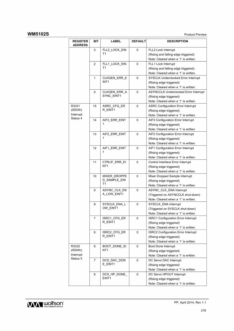
WM5102S Product Preview
w PP, April 2014, Rev 1.1
216
REGISTER ADDRESS
BIT LABEL DEFAULT DESCRIPTION
3 FLL2_LOCK_EINT1
0 FLL2 Lock Interrupt
(Rising and falling edge triggered)
Note: Cleared when a ‘1’ is written.
2 FLL1_LOCK_EINT1
0 FLL1 Lock Interrupt
(Rising and falling edge triggered)
Note: Cleared when a ‘1’ is written.
1 CLKGEN_ERR_EINT1
0 SYSCLK Underclocked Error Interrupt
(Rising edge triggered)
Note: Cleared when a ‘1’ is written.
0 CLKGEN_ERR_ASYNC_EINT1
0 ASYNCCLK Underclocked Error Interrupt
(Rising edge triggered)
Note: Cleared when a ‘1’ is written.
R3331 (0D03h)
Interrupt Status 4
15 ASRC_CFG_ERR_EINT1
0 ASRC Configuration Error Interrupt
(Rising edge triggered)
Note: Cleared when a ‘1’ is written.
14 AIF3_ERR_EINT1
0 AIF3 Configuration Error Interrupt
(Rising edge triggered)
Note: Cleared when a ‘1’ is written.
13 AIF2_ERR_EINT1
0 AIF2 Configuration Error Interrupt
(Rising edge triggered)
Note: Cleared when a ‘1’ is written.
12 AIF1_ERR_EINT1
0 AIF1 Configuration Error Interrupt
(Rising edge triggered)
Note: Cleared when a ‘1’ is written.
11 CTRLIF_ERR_EINT1
0 Control Interface Error Interrupt
(Rising edge triggered)
Note: Cleared when a ‘1’ is written.
10 MIXER_DROPPED_SAMPLE_EINT1
0 Mixer Dropped Sample Interrupt
(Rising edge triggered)
Note: Cleared when a ‘1’ is written.
9 ASYNC_CLK_ENA_LOW_EINT1
0 ASYNC_CLK_ENA Interrupt
(Triggered on ASYNCCLK shut-down)
Note: Cleared when a ‘1’ is written.
8 SYSCLK_ENA_LOW_EINT1
0 SYSCLK_ENA Interrupt
(Triggered on SYSCLK shut-down)
Note: Cleared when a ‘1’ is written.
7 ISRC1_CFG_ERR_EINT1
0 ISRC1 Configuration Error Interrupt
(Rising edge triggered)
Note: Cleared when a ‘1’ is written.
6 ISRC2_CFG_ERR_EINT1
0 ISRC2 Configuration Error Interrupt
(Rising edge triggered)
Note: Cleared when a ‘1’ is written.
R3332 (0D04h)
Interrupt Status 5
8 BOOT_DONE_EINT1
0 Boot Done Interrupt
(Rising edge triggered)
Note: Cleared when a ‘1’ is written.
7 DCS_DAC_DONE_EINT1
0 DC Servo DAC Interrupt
(Rising edge triggered)
Note: Cleared when a ‘1’ is written.
6 DCS_HP_DONE_EINT1
0 DC Servo HPOUT Interrupt
(Rising edge triggered)
Note: Cleared when a ‘1’ is written.
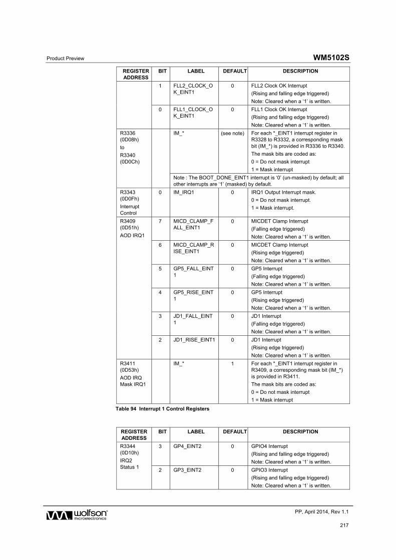
Product Preview WM5102S
w PP, April 2014, Rev 1.1
217
REGISTER ADDRESS
BIT LABEL DEFAULT DESCRIPTION
1 FLL2_CLOCK_OK_EINT1
0 FLL2 Clock OK Interrupt
(Rising and falling edge triggered)
Note: Cleared when a ‘1’ is written.
0 FLL1_CLOCK_OK_EINT1
0 FLL1 Clock OK Interrupt
(Rising and falling edge triggered)
Note: Cleared when a ‘1’ is written.
R3336 (0D08h)
to
R3340 (0D0Ch)
IM_* (see note) For each *_EINT1 interrupt register in R3328 to R3332, a corresponding mask bit (IM_*) is provided in R3336 to R3340.
The mask bits are coded as:
0 = Do not mask interrupt
1 = Mask interrupt
Note : The BOOT_DONE_EINT1 interrupt is ‘0’ (un-masked) by default; all other interrupts are ‘1’ (masked) by default.
R3343 (0D0Fh)
Interrupt Control
0 IM_IRQ1 0 IRQ1 Output Interrupt mask.
0 = Do not mask interrupt.
1 = Mask interrupt.
R3409 (0D51h)
AOD IRQ1
7 MICD_CLAMP_FALL_EINT1
0 MICDET Clamp Interrupt
(Falling edge triggered)
Note: Cleared when a ‘1’ is written.
6 MICD_CLAMP_RISE_EINT1
0 MICDET Clamp Interrupt
(Rising edge triggered)
Note: Cleared when a ‘1’ is written.
5 GP5_FALL_EINT1
0 GP5 Interrupt
(Falling edge triggered)
Note: Cleared when a ‘1’ is written.
4 GP5_RISE_EINT1
0 GP5 Interrupt
(Rising edge triggered)
Note: Cleared when a ‘1’ is written.
3 JD1_FALL_EINT1
0 JD1 Interrupt
(Falling edge triggered)
Note: Cleared when a ‘1’ is written.
2 JD1_RISE_EINT1 0 JD1 Interrupt
(Rising edge triggered)
Note: Cleared when a ‘1’ is written.
R3411 (0D53h)
AOD IRQ Mask IRQ1
IM_* 1 For each *_EINT1 interrupt register in R3409, a corresponding mask bit (IM_*) is provided in R3411.
The mask bits are coded as:
0 = Do not mask interrupt
1 = Mask interrupt
Table 94 Interrupt 1 Control Registers
REGISTER ADDRESS
BIT LABEL DEFAULT DESCRIPTION
R3344 (0D10h)
IRQ2 Status 1
3 GP4_EINT2 0 GPIO4 Interrupt
(Rising and falling edge triggered)
Note: Cleared when a ‘1’ is written.
2 GP3_EINT2 0 GPIO3 Interrupt
(Rising and falling edge triggered)
Note: Cleared when a ‘1’ is written.
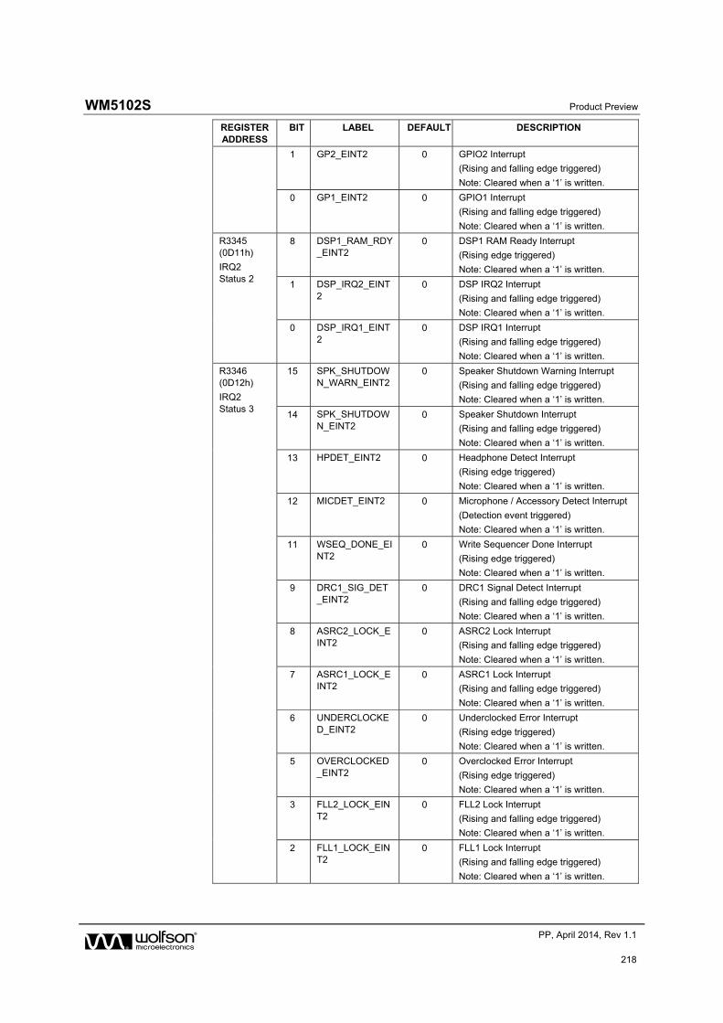
WM5102S Product Preview
w PP, April 2014, Rev 1.1
218
REGISTER ADDRESS
BIT LABEL DEFAULT DESCRIPTION
1 GP2_EINT2 0 GPIO2 Interrupt
(Rising and falling edge triggered)
Note: Cleared when a ‘1’ is written.
0 GP1_EINT2 0 GPIO1 Interrupt
(Rising and falling edge triggered)
Note: Cleared when a ‘1’ is written.
R3345 (0D11h)
IRQ2 Status 2
8 DSP1_RAM_RDY_EINT2
0 DSP1 RAM Ready Interrupt
(Rising edge triggered)
Note: Cleared when a ‘1’ is written.
1 DSP_IRQ2_EINT2
0 DSP IRQ2 Interrupt
(Rising and falling edge triggered)
Note: Cleared when a ‘1’ is written.
0 DSP_IRQ1_EINT2
0 DSP IRQ1 Interrupt
(Rising and falling edge triggered)
Note: Cleared when a ‘1’ is written.
R3346 (0D12h)
IRQ2 Status 3
15 SPK_SHUTDOWN_WARN_EINT2
0 Speaker Shutdown Warning Interrupt
(Rising and falling edge triggered)
Note: Cleared when a ‘1’ is written.
14 SPK_SHUTDOWN_EINT2
0 Speaker Shutdown Interrupt
(Rising and falling edge triggered)
Note: Cleared when a ‘1’ is written.
13 HPDET_EINT2 0 Headphone Detect Interrupt
(Rising edge triggered)
Note: Cleared when a ‘1’ is written.
12 MICDET_EINT2 0 Microphone / Accessory Detect Interrupt
(Detection event triggered)
Note: Cleared when a ‘1’ is written.
11 WSEQ_DONE_EINT2
0 Write Sequencer Done Interrupt
(Rising edge triggered)
Note: Cleared when a ‘1’ is written.
9 DRC1_SIG_DET_EINT2
0 DRC1 Signal Detect Interrupt
(Rising and falling edge triggered)
Note: Cleared when a ‘1’ is written.
8 ASRC2_LOCK_EINT2
0 ASRC2 Lock Interrupt
(Rising and falling edge triggered)
Note: Cleared when a ‘1’ is written.
7 ASRC1_LOCK_EINT2
0 ASRC1 Lock Interrupt
(Rising and falling edge triggered)
Note: Cleared when a ‘1’ is written.
6 UNDERCLOCKED_EINT2
0 Underclocked Error Interrupt
(Rising edge triggered)
Note: Cleared when a ‘1’ is written.
5 OVERCLOCKED_EINT2
0 Overclocked Error Interrupt
(Rising edge triggered)
Note: Cleared when a ‘1’ is written.
3 FLL2_LOCK_EINT2
0 FLL2 Lock Interrupt
(Rising and falling edge triggered)
Note: Cleared when a ‘1’ is written.
2 FLL1_LOCK_EINT2
0 FLL1 Lock Interrupt
(Rising and falling edge triggered)
Note: Cleared when a ‘1’ is written.
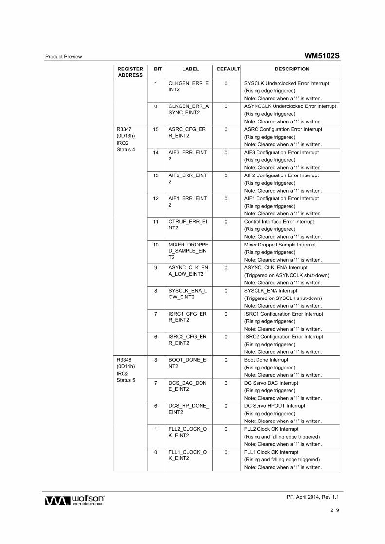
Product Preview WM5102S
w PP, April 2014, Rev 1.1
219
REGISTER ADDRESS
BIT LABEL DEFAULT DESCRIPTION
1 CLKGEN_ERR_EINT2
0 SYSCLK Underclocked Error Interrupt
(Rising edge triggered)
Note: Cleared when a ‘1’ is written.
0 CLKGEN_ERR_ASYNC_EINT2
0 ASYNCCLK Underclocked Error Interrupt
(Rising edge triggered)
Note: Cleared when a ‘1’ is written.
R3347 (0D13h)
IRQ2 Status 4
15 ASRC_CFG_ERR_EINT2
0 ASRC Configuration Error Interrupt
(Rising edge triggered)
Note: Cleared when a ‘1’ is written.
14 AIF3_ERR_EINT2
0 AIF3 Configuration Error Interrupt
(Rising edge triggered)
Note: Cleared when a ‘1’ is written.
13 AIF2_ERR_EINT2
0 AIF2 Configuration Error Interrupt
(Rising edge triggered)
Note: Cleared when a ‘1’ is written.
12 AIF1_ERR_EINT2
0 AIF1 Configuration Error Interrupt
(Rising edge triggered)
Note: Cleared when a ‘1’ is written.
11 CTRLIF_ERR_EINT2
0 Control Interface Error Interrupt
(Rising edge triggered)
Note: Cleared when a ‘1’ is written.
10 MIXER_DROPPED_SAMPLE_EINT2
Mixer Dropped Sample Interrupt
(Rising edge triggered)
Note: Cleared when a ‘1’ is written.
9 ASYNC_CLK_ENA_LOW_EINT2
0 ASYNC_CLK_ENA Interrupt
(Triggered on ASYNCCLK shut-down)
Note: Cleared when a ‘1’ is written.
8 SYSCLK_ENA_LOW_EINT2
0 SYSCLK_ENA Interrupt
(Triggered on SYSCLK shut-down)
Note: Cleared when a ‘1’ is written.
7 ISRC1_CFG_ERR_EINT2
0 ISRC1 Configuration Error Interrupt
(Rising edge triggered)
Note: Cleared when a ‘1’ is written.
6 ISRC2_CFG_ERR_EINT2
0 ISRC2 Configuration Error Interrupt
(Rising edge triggered)
Note: Cleared when a ‘1’ is written.
R3348 (0D14h)
IRQ2 Status 5
8 BOOT_DONE_EINT2
0 Boot Done Interrupt
(Rising edge triggered)
Note: Cleared when a ‘1’ is written.
7 DCS_DAC_DONE_EINT2
0 DC Servo DAC Interrupt
(Rising edge triggered)
Note: Cleared when a ‘1’ is written.
6 DCS_HP_DONE_EINT2
0 DC Servo HPOUT Interrupt
(Rising edge triggered)
Note: Cleared when a ‘1’ is written.
1 FLL2_CLOCK_OK_EINT2
0 FLL2 Clock OK Interrupt
(Rising and falling edge triggered)
Note: Cleared when a ‘1’ is written.
0 FLL1_CLOCK_OK_EINT2
0 FLL1 Clock OK Interrupt
(Rising and falling edge triggered)
Note: Cleared when a ‘1’ is written.
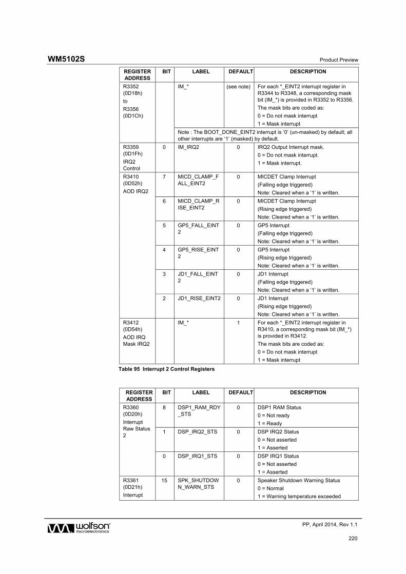
WM5102S Product Preview
w PP, April 2014, Rev 1.1
220
REGISTER ADDRESS
BIT LABEL DEFAULT DESCRIPTION
R3352 (0D18h)
to
R3356 (0D1Ch)
IM_* (see note) For each *_EINT2 interrupt register in R3344 to R3348, a corresponding mask bit (IM_*) is provided in R3352 to R3356.
The mask bits are coded as:
0 = Do not mask interrupt
1 = Mask interrupt
Note : The BOOT_DONE_EINT2 interrupt is ‘0’ (un-masked) by default; all other interrupts are ‘1’ (masked) by default.
R3359 (0D1Fh)
IRQ2 Control
0 IM_IRQ2 0 IRQ2 Output Interrupt mask.
0 = Do not mask interrupt.
1 = Mask interrupt.
R3410 (0D52h)
AOD IRQ2
7 MICD_CLAMP_FALL_EINT2
0 MICDET Clamp Interrupt
(Falling edge triggered)
Note: Cleared when a ‘1’ is written.
6 MICD_CLAMP_RISE_EINT2
0 MICDET Clamp Interrupt
(Rising edge triggered)
Note: Cleared when a ‘1’ is written.
5 GP5_FALL_EINT2
0 GP5 Interrupt
(Falling edge triggered)
Note: Cleared when a ‘1’ is written.
4 GP5_RISE_EINT2
0 GP5 Interrupt
(Rising edge triggered)
Note: Cleared when a ‘1’ is written.
3 JD1_FALL_EINT2
0 JD1 Interrupt
(Falling edge triggered)
Note: Cleared when a ‘1’ is written.
2 JD1_RISE_EINT2 0 JD1 Interrupt
(Rising edge triggered)
Note: Cleared when a ‘1’ is written.
R3412 (0D54h)
AOD IRQ Mask IRQ2
IM_* 1 For each *_EINT2 interrupt register in R3410, a corresponding mask bit (IM_*) is provided in R3412.
The mask bits are coded as:
0 = Do not mask interrupt
1 = Mask interrupt
Table 95 Interrupt 2 Control Registers
REGISTER ADDRESS
BIT LABEL DEFAULT DESCRIPTION
R3360 (0D20h)
Interrupt Raw Status 2
8 DSP1_RAM_RDY_STS
0 DSP1 RAM Status
0 = Not ready
1 = Ready
1 DSP_IRQ2_STS 0 DSP IRQ2 Status
0 = Not asserted
1 = Asserted
0 DSP_IRQ1_STS 0 DSP IRQ1 Status
0 = Not asserted
1 = Asserted
R3361 (0D21h)
Interrupt
15 SPK_SHUTDOWN_WARN_STS
0 Speaker Shutdown Warning Status
0 = Normal
1 = Warning temperature exceeded
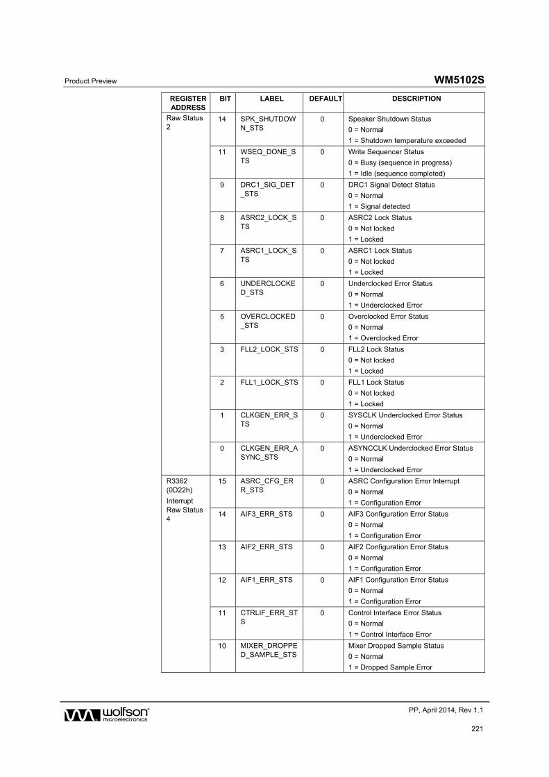
Product Preview WM5102S
w PP, April 2014, Rev 1.1
221
REGISTER ADDRESS
BIT LABEL DEFAULT DESCRIPTION
Raw Status 2
14 SPK_SHUTDOWN_STS
0 Speaker Shutdown Status
0 = Normal
1 = Shutdown temperature exceeded
11 WSEQ_DONE_STS
0 Write Sequencer Status
0 = Busy (sequence in progress)
1 = Idle (sequence completed)
9 DRC1_SIG_DET_STS
0 DRC1 Signal Detect Status
0 = Normal
1 = Signal detected
8 ASRC2_LOCK_STS
0 ASRC2 Lock Status
0 = Not locked
1 = Locked
7 ASRC1_LOCK_STS
0 ASRC1 Lock Status
0 = Not locked
1 = Locked
6 UNDERCLOCKED_STS
0 Underclocked Error Status
0 = Normal
1 = Underclocked Error
5 OVERCLOCKED_STS
0 Overclocked Error Status
0 = Normal
1 = Overclocked Error
3 FLL2_LOCK_STS 0 FLL2 Lock Status
0 = Not locked
1 = Locked
2 FLL1_LOCK_STS 0 FLL1 Lock Status
0 = Not locked
1 = Locked
1 CLKGEN_ERR_STS
0 SYSCLK Underclocked Error Status
0 = Normal
1 = Underclocked Error
0 CLKGEN_ERR_ASYNC_STS
0 ASYNCCLK Underclocked Error Status
0 = Normal
1 = Underclocked Error
R3362 (0D22h)
Interrupt Raw Status 4
15 ASRC_CFG_ERR_STS
0 ASRC Configuration Error Interrupt
0 = Normal
1 = Configuration Error
14 AIF3_ERR_STS 0 AIF3 Configuration Error Status
0 = Normal
1 = Configuration Error
13 AIF2_ERR_STS 0 AIF2 Configuration Error Status
0 = Normal
1 = Configuration Error
12 AIF1_ERR_STS 0 AIF1 Configuration Error Status
0 = Normal
1 = Configuration Error
11 CTRLIF_ERR_STS
0 Control Interface Error Status
0 = Normal
1 = Control Interface Error
10 MIXER_DROPPED_SAMPLE_STS
Mixer Dropped Sample Status
0 = Normal
1 = Dropped Sample Error
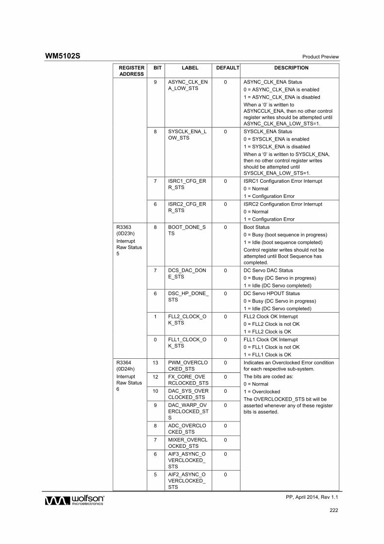
WM5102S Product Preview
w PP, April 2014, Rev 1.1
222
REGISTER ADDRESS
BIT LABEL DEFAULT DESCRIPTION
9 ASYNC_CLK_ENA_LOW_STS
0 ASYNC_CLK_ENA Status
0 = ASYNC_CLK_ENA is enabled
1 = ASYNC_CLK_ENA is disabled
When a ‘0’ is written to ASYNCCLK_ENA, then no other control register writes should be attempted until ASYNC_CLK_ENA_LOW_STS=1.
8 SYSCLK_ENA_LOW_STS
0 SYSCLK_ENA Status
0 = SYSCLK_ENA is enabled
1 = SYSCLK_ENA is disabled
When a ‘0’ is written to SYSCLK_ENA, then no other control register writes should be attempted until SYSCLK_ENA_LOW_STS=1.
7 ISRC1_CFG_ERR_STS
0 ISRC1 Configuration Error Interrupt
0 = Normal
1 = Configuration Error
6 ISRC2_CFG_ERR_STS
0 ISRC2 Configuration Error Interrupt
0 = Normal
1 = Configuration Error
R3363 (0D23h)
Interrupt Raw Status 5
8 BOOT_DONE_STS
0 Boot Status
0 = Busy (boot sequence in progress)
1 = Idle (boot sequence completed)
Control register writes should not be attempted until Boot Sequence has completed.
7 DCS_DAC_DONE_STS
0 DC Servo DAC Status
0 = Busy (DC Servo in progress)
1 = Idle (DC Servo completed)
6 DSC_HP_DONE_STS
0 DC Servo HPOUT Status
0 = Busy (DC Servo in progress)
1 = Idle (DC Servo completed)
1 FLL2_CLOCK_OK_STS
0 FLL2 Clock OK Interrupt
0 = FLL2 Clock is not OK
1 = FLL2 Clock is OK
0 FLL1_CLOCK_OK_STS
0 FLL1 Clock OK Interrupt
0 = FLL1 Clock is not OK
1 = FLL1 Clock is OK
R3364 (0D24h)
Interrupt Raw Status 6
13 PWM_OVERCLOCKED_STS
0 Indicates an Overclocked Error condition for each respective sub-system.
The bits are coded as:
0 = Normal
1 = Overclocked
The OVERCLOCKED_STS bit will be asserted whenever any of these register bits is asserted.
12 FX_CORE_OVERCLOCKED_STS
0
10 DAC_SYS_OVERCLOCKED_STS
0
9 DAC_WARP_OVERCLOCKED_STS
0
8 ADC_OVERCLOCKED_STS
0
7 MIXER_OVERCLOCKED_STS
0
6 AIF3_ASYNC_OVERCLOCKED_STS
0
5 AIF2_ASYNC_OVERCLOCKED_STS
0
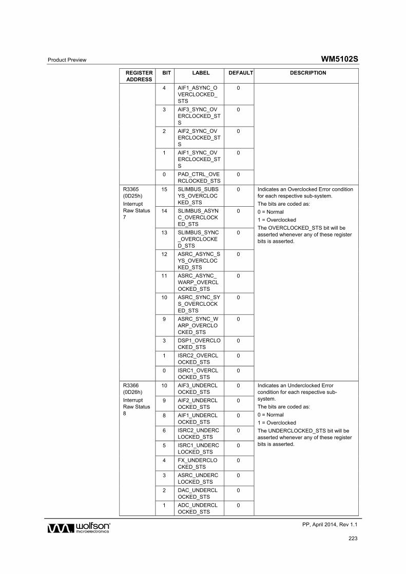
Product Preview WM5102S
w PP, April 2014, Rev 1.1
223
REGISTER ADDRESS
BIT LABEL DEFAULT DESCRIPTION
4 AIF1_ASYNC_OVERCLOCKED_STS
0
3 AIF3_SYNC_OVERCLOCKED_STS
0
2 AIF2_SYNC_OVERCLOCKED_STS
0
1 AIF1_SYNC_OVERCLOCKED_STS
0
0 PAD_CTRL_OVERCLOCKED_STS
0
R3365 (0D25h)
Interrupt Raw Status 7
15 SLIMBUS_SUBSYS_OVERCLOCKED_STS
0 Indicates an Overclocked Error condition for each respective sub-system.
The bits are coded as:
0 = Normal
1 = Overclocked
The OVERCLOCKED_STS bit will be asserted whenever any of these register bits is asserted.
14 SLIMBUS_ASYNC_OVERCLOCKED_STS
0
13 SLIMBUS_SYNC_OVERCLOCKED_STS
0
12 ASRC_ASYNC_SYS_OVERCLOCKED_STS
0
11 ASRC_ASYNC_WARP_OVERCLOCKED_STS
0
10 ASRC_SYNC_SYS_OVERCLOCKED_STS
0
9 ASRC_SYNC_WARP_OVERCLOCKED_STS
0
3 DSP1_OVERCLOCKED_STS
0
1 ISRC2_OVERCLOCKED_STS
0
0 ISRC1_OVERCLOCKED_STS
0
R3366 (0D26h)
Interrupt Raw Status 8
10 AIF3_UNDERCLOCKED_STS
0 Indicates an Underclocked Error condition for each respective sub-system.
The bits are coded as:
0 = Normal
1 = Overclocked
The UNDERCLOCKED_STS bit will be asserted whenever any of these register bits is asserted.
9 AIF2_UNDERCLOCKED_STS
0
8 AIF1_UNDERCLOCKED_STS
0
6 ISRC2_UNDERCLOCKED_STS
0
5 ISRC1_UNDERCLOCKED_STS
0
4 FX_UNDERCLOCKED_STS
0
3 ASRC_UNDERCLOCKED_STS
0
2 DAC_UNDERCLOCKED_STS
0
1 ADC_UNDERCLOCKED_STS
0
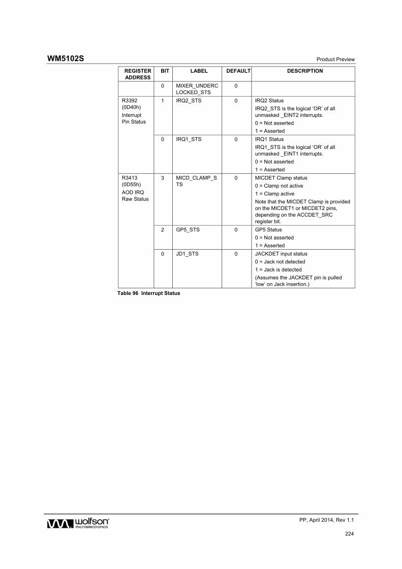
WM5102S Product Preview
w PP, April 2014, Rev 1.1
224
REGISTER ADDRESS
BIT LABEL DEFAULT DESCRIPTION
0 MIXER_UNDERCLOCKED_STS
0
R3392 (0D40h)
Interrupt Pin Status
1 IRQ2_STS 0 IRQ2 Status
IRQ2_STS is the logical ‘OR’ of all unmasked _EINT2 interrupts.
0 = Not asserted
1 = Asserted
0 IRQ1_STS 0 IRQ1 Status
IRQ1_STS is the logical ‘OR’ of all unmasked _EINT1 interrupts.
0 = Not asserted
1 = Asserted
R3413 (0D55h)
AOD IRQ Raw Status
3 MICD_CLAMP_STS
0 MICDET Clamp status
0 = Clamp not active
1 = Clamp active
Note that the MICDET Clamp is provided on the MICDET1 or MICDET2 pins, depending on the ACCDET_SRC register bit.
2 GP5_STS 0 GP5 Status
0 = Not asserted
1 = Asserted
0 JD1_STS 0 JACKDET input status
0 = Jack not detected
1 = Jack is detected
(Assumes the JACKDET pin is pulled ‘low’ on Jack insertion.)
Table 96 Interrupt Status
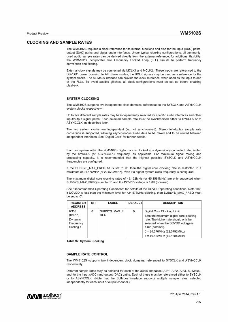
Product Preview WM5102S
w PP, April 2014, Rev 1.1
225
CLOCKING AND SAMPLE RATES
The WM5102S requires a clock reference for its internal functions and also for the input (ADC) paths, output (DAC) paths and digital audio interfaces. Under typical clocking configurations, all commonly-used audio sample rates can be derived directly from the external reference; for additional flexibility, the WM5102S incorporates two Frequency Locked Loop (FLL) circuits to perform frequency conversion and filtering.
External clock signals may be connected via MCLK1 and MCLK2. (These inputs are referenced to the DBVDD1 power domain.) In AIF Slave modes, the BCLK signals may be used as a reference for the system clocks. The SLIMbus interface can provide the clock reference, when used as the input to one of the FLLs. To avoid audible glitches, all clock configurations must be set up before enabling playback.
SYSTEM CLOCKING
The WM5102S supports two independent clock domains, referenced to the SYSCLK and ASYNCCLK system clocks respectively.
Up to five different sample rates may be independently selected for specific audio interfaces and other input/output signal paths. Each selected sample rate must be synchronised either to SYSCLK or to ASYNCCLK, as described later.
The two system clocks are independent (ie. not synchronised). Stereo full-duplex sample rate conversion is supported, allowing asynchronous audio data to be mixed and to be routed between independent interfaces. See “Digital Core” for further details.
Each subsystem within the WM5102S digital core is clocked at a dynamically-controlled rate, limited by the SYSCLK (or ASYNCCLK) frequency, as applicable. For maximum signal mixing and processing capacity, it is recommended that the highest possible SYSCLK and ASYNCCLK frequencies are configured.
If the SUBSYS_MAX_FREQ bit is set to ‘0’, then the digital core clocking rate is restricted to a maximum of 24.576MHz (or 22.5792MHz), even if a higher system clock frequency is configured.
The maximum digital core clocking rates of 49.152MHz (or 45.1584MHz) are only supported when SUBSYS_MAX_FREQ is set to ‘1’, and the DCVDD voltage is 1.8V (nominal).
See “Recommended Operating Conditions” for details of the DCVDD operating conditions. Note that, if DCVDD is less than the minimum level for >24.576MHz clocking, then SUBSYS_MAX_FREQ must be set to ‘0’.
REGISTER ADDRESS
BIT LABEL DEFAULT DESCRIPTION
R353 (0161h)
Dynamic Frequency Scaling 1
0 SUBSYS_MAX_FREQ
0 Digital Core Clocking Limit
Sets the maximum digital core clocking rate. The higher rate should only be selected when the DCVDD voltage is 1.8V (nominal).
0 = 24.576MHz (22.5792MHz)
1 = 49.152MHz (45.1584MHz)
Table 97 System Clocking
SAMPLE RATE CONTROL
The WM5102S supports two independent clock domains, referenced to SYSCLK and ASYNCCLK respectively.
Different sample rates may be selected for each of the audio interfaces (AIF1, AIF2, AIF3, SLIMbus), and for the input (ADC) and output (DAC) paths. Each of these must be referenced either to SYSCLK or to ASYNCCLK. (Note that the SLIMbus interface supports multiple sample rates, selected independently for each input or output channel.)
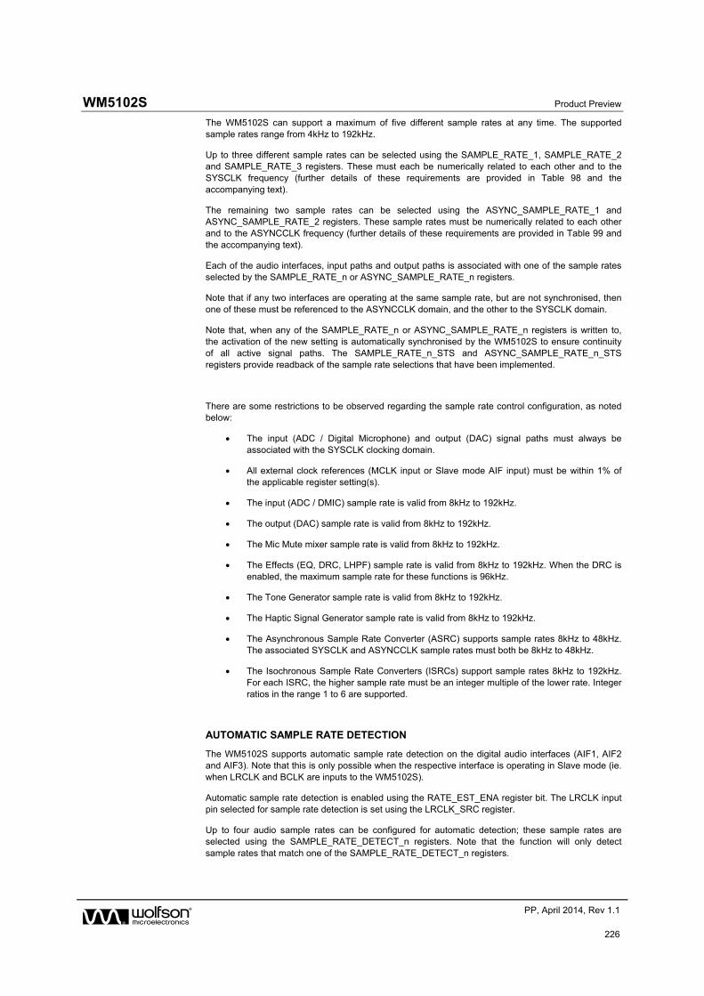
WM5102S Product Preview
w PP, April 2014, Rev 1.1
226
The WM5102S can support a maximum of five different sample rates at any time. The supported sample rates range from 4kHz to 192kHz.
Up to three different sample rates can be selected using the SAMPLE_RATE_1, SAMPLE_RATE_2 and SAMPLE_RATE_3 registers. These must each be numerically related to each other and to the SYSCLK frequency (further details of these requirements are provided in Table 98 and the accompanying text).
The remaining two sample rates can be selected using the ASYNC_SAMPLE_RATE_1 and ASYNC_SAMPLE_RATE_2 registers. These sample rates must be numerically related to each other and to the ASYNCCLK frequency (further details of these requirements are provided in Table 99 and the accompanying text).
Each of the audio interfaces, input paths and output paths is associated with one of the sample rates selected by the SAMPLE_RATE_n or ASYNC_SAMPLE_RATE_n registers.
Note that if any two interfaces are operating at the same sample rate, but are not synchronised, then one of these must be referenced to the ASYNCCLK domain, and the other to the SYSCLK domain.
Note that, when any of the SAMPLE_RATE_n or ASYNC_SAMPLE_RATE_n registers is written to, the activation of the new setting is automatically synchronised by the WM5102S to ensure continuity of all active signal paths. The SAMPLE_RATE_n_STS and ASYNC_SAMPLE_RATE_n_STS registers provide readback of the sample rate selections that have been implemented.
There are some restrictions to be observed regarding the sample rate control configuration, as noted below:
The input (ADC / Digital Microphone) and output (DAC) signal paths must always be associated with the SYSCLK clocking domain.
All external clock references (MCLK input or Slave mode AIF input) must be within 1% of the applicable register setting(s).
The input (ADC / DMIC) sample rate is valid from 8kHz to 192kHz.
The output (DAC) sample rate is valid from 8kHz to 192kHz.
The Mic Mute mixer sample rate is valid from 8kHz to 192kHz.
The Effects (EQ, DRC, LHPF) sample rate is valid from 8kHz to 192kHz. When the DRC is enabled, the maximum sample rate for these functions is 96kHz.
The Tone Generator sample rate is valid from 8kHz to 192kHz.
The Haptic Signal Generator sample rate is valid from 8kHz to 192kHz.
The Asynchronous Sample Rate Converter (ASRC) supports sample rates 8kHz to 48kHz. The associated SYSCLK and ASYNCCLK sample rates must both be 8kHz to 48kHz.
The Isochronous Sample Rate Converters (ISRCs) support sample rates 8kHz to 192kHz. For each ISRC, the higher sample rate must be an integer multiple of the lower rate. Integer ratios in the range 1 to 6 are supported.
AUTOMATIC SAMPLE RATE DETECTION
The WM5102S supports automatic sample rate detection on the digital audio interfaces (AIF1, AIF2 and AIF3). Note that this is only possible when the respective interface is operating in Slave mode (ie. when LRCLK and BCLK are inputs to the WM5102S).
Automatic sample rate detection is enabled using the RATE_EST_ENA register bit. The LRCLK input pin selected for sample rate detection is set using the LRCLK_SRC register.
Up to four audio sample rates can be configured for automatic detection; these sample rates are selected using the SAMPLE_RATE_DETECT_n registers. Note that the function will only detect sample rates that match one of the SAMPLE_RATE_DETECT_n registers.
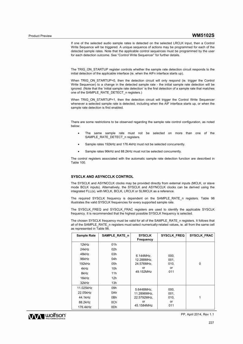
Product Preview WM5102S
w PP, April 2014, Rev 1.1
227
If one of the selected audio sample rates is detected on the selected LRCLK input, then a Control Write Sequence will be triggered. A unique sequence of actions may be programmed for each of the detected sample rates. Note that the applicable control sequences must be programmed by the user for each detection outcome. See “Control Write Sequencer” for further details.
The TRIG_ON_STARTUP register controls whether the sample rate detection circuit responds to the initial detection of the applicable interface (ie. when the AIFn interface starts up).
When TRIG_ON_STARTUP=0, then the detection circuit will only respond (ie. trigger the Control Write Sequencer) to a change in the detected sample rate - the initial sample rate detection will be ignored. (Note that the ‘initial sample rate detection’ is the first detection of a sample rate that matches one of the SAMPLE_RATE_DETECT_n registers.)
When TRIG_ON_STARTUP=1, then the detection circuit will trigger the Control Write Sequencer whenever a selected sample rate is detected, including when the AIF interface starts up, or when the sample rate detection is first enabled.
There are some restrictions to be observed regarding the sample rate control configuration, as noted below:
The same sample rate must not be selected on more than one of the SAMPLE_RATE_DETECT_n registers.
Sample rates 192kHz and 176.4kHz must not be selected concurrently.
Sample rates 96kHz and 88.2kHz must not be selected concurrently.
The control registers associated with the automatic sample rate detection function are described in Table 100.
SYSCLK AND ASYNCCLK CONTROL
The SYSCLK and ASYNCCLK clocks may be provided directly from external inputs (MCLK, or slave mode BCLK inputs). Alternatively, the SYSCLK and ASYNCCLK clocks can be derived using the integrated FLL(s), with MCLK, BCLK, LRCLK or SLIMCLK as a reference.
The required SYSCLK frequency is dependent on the SAMPLE_RATE_n registers. Table 98 illustrates the valid SYSCLK frequencies for every supported sample rate.
The SYSCLK_FREQ and SYSCLK_FRAC registers are used to identify the applicable SYSCLK frequency. It is recommended that the highest possible SYSCLK frequency is selected.
The chosen SYSCLK frequency must be valid for all of the SAMPLE_RATE_n registers. It follows that all of the SAMPLE_RATE_n registers must select numerically-related values, ie. all from the same cell as represented in Table 98.
Sample Rate SAMPLE_RATE_n SYSCLK Frequency
SYSCLK_FREQ SYSCLK_FRAC
12kHz
24kHz
48kHz
96kHz
192kHz
4kHz
8kHz
16kHz
32kHz
01h
02h
03h
04h
05h
10h
11h
12h
13h
6.144MHz, 12.288MHz, 24.576MHz,
or 49.152MHz
000, 001, 010, or
011
0
11.025kHz
22.05kHz
44.1kHz
88.2kHz
176.4kHz
09h
0Ah
0Bh
0Ch
0Dh
5.6448MHz, 11.2896MHz, 22.5792MHz,
or 45.1584MHz
000, 001, 010, or
011
1
WM5102S Product Preview
w PP, April 2014, Rev 1.1
228
Sample Rate SAMPLE_RATE_n SYSCLK Frequency
SYSCLK_FREQ SYSCLK_FRAC
Note that each of the SAMPLE_RATE_n registers must select a sample rate value from the same group in the two lists above.
Table 98 SYSCLK Frequency Selection
The required ASYNCCLK frequency is dependent on the ASYNC_SAMPLE_RATE_n registers. Table 99 illustrates the valid ASYNCCLK frequencies for every supported sample rate.
The ASYNC_CLK_FREQ register is used to identify the applicable ASYNCCLK frequency. It is recommended that the highest possible ASYNCCLK frequency is selected.
Note that, if all the sample rates in the system are synchronised to SYSCLK, then the ASYNCCLK may not be required at all. In this case, the ASYNCCLK should be disabled (see Table 100), and the associated register values are not important.
Sample Rate ASYNC_SAMPLE_RATE_n ASYNCCLK Frequency
ASYNC_CLK_FREQ
12kHz
24kHz
48kHz
96kHz
192kHz
4kHz
8kHz
16kHz
32kHz
01h
02h
03h
04h
05h
10h
11h
12h
13h
6.144MHz, 12.288MHz, 24.576MHz,
or 49.152MHz
000, 001, 010, or
011
11.025kHz
22.05kHz
44.1kHz
88.2kHz
176.4kHz
09h
0Ah
0Bh
0Ch
0Dh
5.6448MHz, 11.2896MHz, 22.5792MHz
or 45.1584MHz
000, 001, 010, or
011
Note that each of the ASYNC_SAMPLE_RATE_n registers must select a sample rate value from the same group in the two lists above.
Table 99 ASYNCCLK Frequency Selection
The WM5102S supports automatic clocking configuration. The programmable dividers associated with the ADCs, DACs and all DSP functions are configured automatically, with values determined from the SYSCLK_FREQ, SAMPLE_RATE_n, ASYNC_CLK_FREQ and ASYNC_SAMPLE_RATE_n fields.
Note that the digital audio interface (AIF) clocking rates must be configured separately.
The sample rates of each AIF, the input (ADC) paths, output (DAC) paths and DSP functions are selected as described in the respective sections. Stereo full-duplex sample rate conversion is supported in multiple configurations to allow digital audio to be routed between interfaces and for asynchronous audio data to be mixed. See “Digital Core” for further details.
The SYSCLK_SRC register is used to select the SYSCLK source, as described in Table 100. The source may be MCLKn, AIFnBCLK or FLLn. If one of the Frequency Locked Loop (FLL) circuits is selected as the source, then the relevant FLL must be enabled and configured, as described later.
The SYSCLK_FREQ and SYSCLK_FRAC registers are set according to the frequency of the selected SYSCLK source.
The SYSCLK-referenced circuits within the digital core are clocked at a dynamically-controlled rate, limited by the SYSCLK frequency itself. For maximum signal mixing and processing capacity, it is recommended that the highest possible SYSCLK frequency is configured.
Product Preview WM5102S
w PP, April 2014, Rev 1.1
229
If the SUBSYS_MAX_FREQ bit is set to ‘0’, then the digital core clocking rate is restricted to a maximum of 24.576MHz (or 22.5792MHz), even if a higher SYSCLK frequency is configured. The SUBSYS_MAX_FREQ should only be set to ‘1’ when the applicable DCVDD condition is satisfied, as described in Table 97.
The SAMPLE_RATE_n registers are set according to the sample rate(s) that are required by one or more of the WM5102S audio interfaces. The WM5102S supports sample rates ranging from 4kHz to 192kHz.
The SYSCLK signal is enabled by the register bit SYSCLK_ENA. The applicable clock source (MCLKn, AIFnBCLK or FLLn) must be enabled before setting SYSCLK_ENA=1. This bit should be set to 0 when reconfiguring the clock sources (see below for additional requirements when setting SYSCLK_ENA=0).
When disabling SYSCLK, note that all of the input, output or digital core functions associated with the SYSCLK clock domain must be disabled before setting SYSCLK_ENA=0.
When ‘0’ is written to SYSCLK_ENA, the host processor must wait until the WM5102S has shut down the associated functions before issuing any other register write commands. The SYSCLK Enable status can be polled via the SYSCLK_ENA_LOW_STS bit (see Table 96), or else monitored using the Interrupt or GPIO functions.
The SYSCLK Enable status is an input to the Interrupt control circuit and can be used to trigger an Interrupt event - see “Interrupts”. The corresponding Interrupt event indicates that the WM5102S has shut down the SYSCLK functions and is ready to accept register write commands.
The SYSCLK Enable status can be output directly on a GPIO pin as an external indication of the SYSCLK status. See “General Purpose Input / Output” to configure a GPIO pin for this function.
The required control sequence for disabling SYSCLK is summarised below:
Disable all SYSCLK-associated functions (inputs, outputs, digital core)
Set SYSCLK_ENA = 0
Wait until SYSCLK_ENA_LOW = 1 (or wait for the corresponding IRQ/GPIO event)
The ASYNC_CLK_SRC register is used to select the ASYNCCLK source, as described in Table 100. The source may be MCLKn, AIFnBCLK or FLLn. If one of the Frequency Locked Loop (FLL) circuits is selected as the source, then the relevant FLL must be enabled and configured, as described later.
The ASYNC_CLK_FREQ register is set according to the frequency of the selected ASYNCCLK source.
The ASYNCCLK-referenced circuits within the digital core are clocked at a dynamically-controlled rate, limited by the ASYNCCLK frequency itself. For maximum signal mixing and processing capacity, it is recommended that the highest possible ASYNCCLK frequency is configured.
If the SUBSYS_MAX_FREQ bit is set to ‘0’, then the digital core clocking rate is restricted to a maximum of 24.576MHz (or 22.5792MHz), even if a higher ASYNCCLK frequency is configured. The SUBSYS_MAX_FREQ should only be set to ‘1’ when the applicable DCVDD condition is satisfied, as described in Table 97.
The ASYNC_SAMPLE_RATE_n registers are set according to the sample rate(s) of any audio interface that is not synchronised to the SYSCLK clock domain.
The ASYNCCLK signal is enabled by the register bit ASYNC_CLK_ENA. The applicable clock source (MCLKn, AIFnBCLK or FLLn) must be enabled before setting ASYNC_CLK_ENA=1. This bit should be set to 0 when reconfiguring the clock sources (see below for additional requirements when setting ASYNC_CLK_ENA=0).
When disabling ASYNCCLK, note that all of the input, output or digital core functions associated with the ASYNCCLK clock domain must be disabled before setting ASYNC_CLK_ENA=0.
When ‘0’ is written to ASYNC_CLK_ENA, the host processor must wait until the WM5102S has shut down the associated functions before issuing any other register write commands. The ASYNCCLK Enable status can be polled via the ASYNC_CLK_ENA_LOW_STS bit (see Table 96), or else monitored using the Interrupt or GPIO functions.
WM5102S Product Preview
w PP, April 2014, Rev 1.1
230
The ASYNCCLK Enable status is an input to the Interrupt control circuit and can be used to trigger an Interrupt event - see “Interrupts”. The corresponding Interrupt event indicates that the WM5102S has shut down the ASYNCCLK functions and is ready to accept register write commands.
The ASYNCCLK Enable status can be output directly on a GPIO pin as an external indication of the ASYNCCLK status. See “General Purpose Input / Output” to configure a GPIO pin for this function.
The required control sequence for disabling ASYNCCLK is summarised below:
Disable all ASYNCCLK-associated functions (inputs, outputs, digital core)
Set ASYNCCLK_ENA = 0
Wait until ASYNCCLK_ENA_LOW = 1 (or wait for the corresponding IRQ/GPIO event)
The SYSCLK (and ASYNCCLK, when applicable) clocks must be configured and enabled before any audio path is enabled.
The WM5102S performs automatic checks to confirm that the SYSCLK and ASYNCCLK frequencies are high enough to support the commanded signal paths and processing functions. If an attempt is made to enable a signal path or processing function, and there are insufficient SYSCLK or ASYNCCLK cycles to support it, then the attempt will be unsuccessful. (Note that any signal paths that are already active will not be affected under these circumstances.)
An Underclocked Error condition is where there are insufficient clock cycles for the requested functionality, and increasing the SYSCLK or ASYNCCLK frequency (as applicable) should allow the selected configuration to be supported.
An Overclocked Error condition is where the requested functionality cannot be supported, as the clocking requirements of the requested configuration exceed the device limits.
The SYSCLK Underclocked condition, ASYNCCLK Underclocked condition, and other Clocking Error conditions can be monitored using the GPIO and/or Interrupt functions. See “General Purpose Input / Output” and “Interrupts” for further details.
MISCELLANEOUS CLOCK CONTROLS
The WM5102S requires a 32kHz clock for miscellaneous de-bounce functions. This can be generated automatically from SYSCLK, or may be input directly as MCLK1 or MCLK2. The 32kHz clock source is selected using the CLK_32K_SRC register. The 32kHz clock is enabled using the CLK_32K_ENA register.
A clock output (OPCLK) derived from SYSCLK can be output on a GPIO pin. See “General Purpose Input / Output” to configure a GPIO pin for this function.
A clock output (OPCLK_ASYNC) derived from ASYNCCLK can be output on a GPIO pin. See “General Purpose Input / Output” to configure a GPIO pin for this function.
The WM5102S provides integrated pull-down resistors on the MCLK1 and MCLK2 pins. This provides a flexible capability for interfacing with other devices.
The clocking scheme for the WM5102S is illustrated in Figure 68.

Product Preview WM5102S
w PP, April 2014, Rev 1.1
231
MCLK2MCLK1
SYSCLK
SYSCLK_ENA
SA
MP
LE_R
AT
E_1
[4:0
]
SY
SC
LK_F
RA
C
AIF1BCLKAIF2BCLKAIF3BCLK
FLL1_REFCLK_SRC
FLL2_REFCLK_SRC
SA
MP
LE_R
AT
E_2
[4:0
]
SA
MP
LE_R
AT
E_3
[4:0
]
AS
YN
C_S
AM
PLE
_RA
TE
_2 [4
:0]
AS
YN
C_C
LK_F
RE
Q [2
:0]
CLK_32K_SRC
32k Clock
Divider (Auto)
Divider
OPCLK
OPCLK_SELOPCLK_DIV
CLK_32K_ENA
SY
SC
LK_F
RE
Q [
2:0
]
FLL1
ASYNC_CLK_ENA
OPCLK_ENA
ASYNCCLK
Divider
OPCLK_ASYNC
OPCLK_ASYNC_SELOPCLK_ASYNC_DIV
OPCLK_ASYNC_ENA
Automatic Clocking Control
FLLn, AIFnRXLRCLK, and SLIMCLK can also be selected as FLLn input reference.
Divider
FLL1_GPCLK_DIV
GPIO output
FLL1_GPCLK_ENA
SYSCLK_SRC
ASYNC_CLK_SRC
FLL2_OUTDIV
FLL1_OUTDIV
FLL2Divider GPIO output
FLL2_GPCLK_DIV
FLL2_GPCLK_ENA
Divider
Divider
AS
YN
C_S
AM
PLE
_RA
TE
_1 [4
:0]
Figure 68 System Clocking
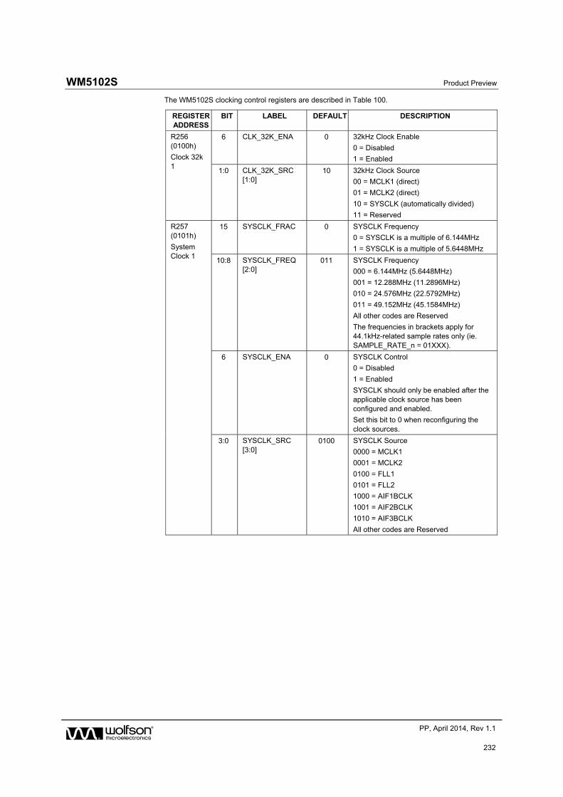
WM5102S Product Preview
w PP, April 2014, Rev 1.1
232
The WM5102S clocking control registers are described in Table 100.
REGISTER ADDRESS
BIT LABEL DEFAULT DESCRIPTION
R256 (0100h)
Clock 32k 1
6 CLK_32K_ENA 0 32kHz Clock Enable
0 = Disabled
1 = Enabled
1:0 CLK_32K_SRC [1:0]
10 32kHz Clock Source
00 = MCLK1 (direct)
01 = MCLK2 (direct)
10 = SYSCLK (automatically divided)
11 = Reserved
R257 (0101h)
System Clock 1
15 SYSCLK_FRAC 0 SYSCLK Frequency
0 = SYSCLK is a multiple of 6.144MHz
1 = SYSCLK is a multiple of 5.6448MHz
10:8 SYSCLK_FREQ [2:0]
011 SYSCLK Frequency
000 = 6.144MHz (5.6448MHz)
001 = 12.288MHz (11.2896MHz)
010 = 24.576MHz (22.5792MHz)
011 = 49.152MHz (45.1584MHz)
All other codes are Reserved
The frequencies in brackets apply for 44.1kHz-related sample rates only (ie. SAMPLE_RATE_n = 01XXX).
6 SYSCLK_ENA 0 SYSCLK Control
0 = Disabled
1 = Enabled
SYSCLK should only be enabled after the applicable clock source has been configured and enabled.
Set this bit to 0 when reconfiguring the clock sources.
3:0 SYSCLK_SRC [3:0]
0100 SYSCLK Source
0000 = MCLK1
0001 = MCLK2
0100 = FLL1
0101 = FLL2
1000 = AIF1BCLK
1001 = AIF2BCLK
1010 = AIF3BCLK
All other codes are Reserved
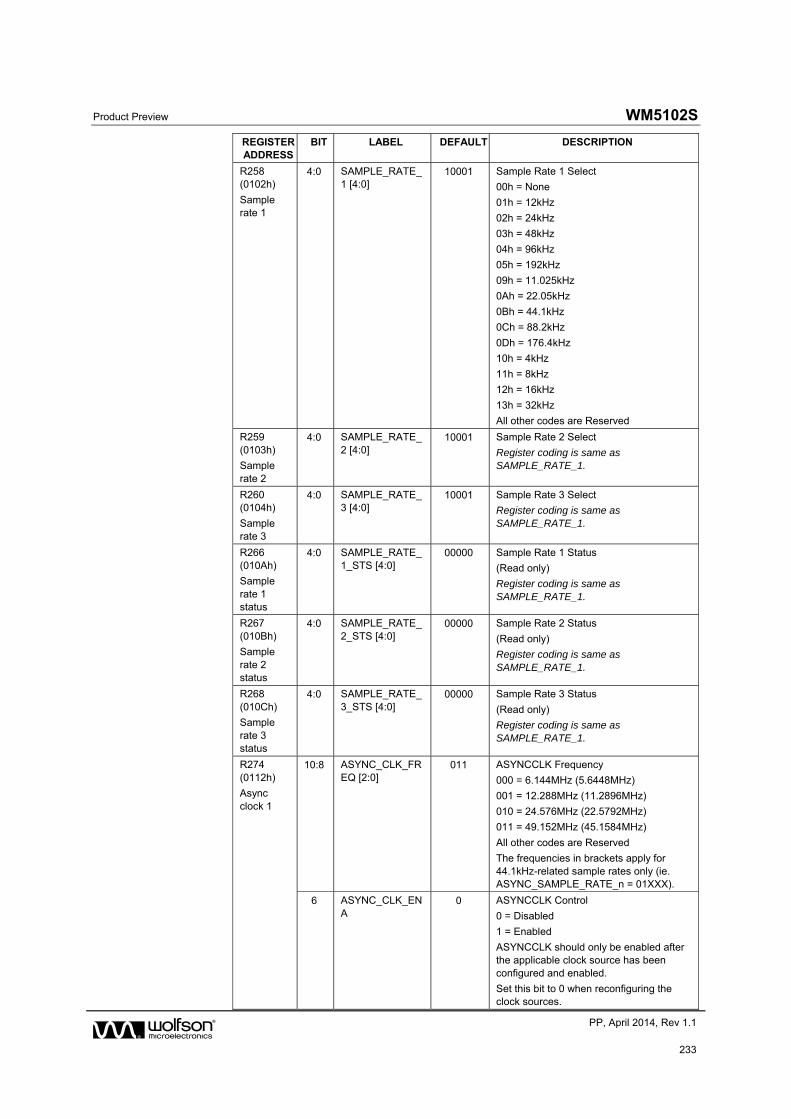
Product Preview WM5102S
w PP, April 2014, Rev 1.1
233
REGISTER ADDRESS
BIT LABEL DEFAULT DESCRIPTION
R258 (0102h)
Sample rate 1
4:0 SAMPLE_RATE_1 [4:0]
10001 Sample Rate 1 Select
00h = None
01h = 12kHz
02h = 24kHz
03h = 48kHz
04h = 96kHz
05h = 192kHz
09h = 11.025kHz
0Ah = 22.05kHz
0Bh = 44.1kHz
0Ch = 88.2kHz
0Dh = 176.4kHz
10h = 4kHz
11h = 8kHz
12h = 16kHz
13h = 32kHz
All other codes are Reserved
R259 (0103h)
Sample rate 2
4:0 SAMPLE_RATE_2 [4:0]
10001 Sample Rate 2 Select
Register coding is same as SAMPLE_RATE_1.
R260 (0104h)
Sample rate 3
4:0 SAMPLE_RATE_3 [4:0]
10001 Sample Rate 3 Select
Register coding is same as SAMPLE_RATE_1.
R266 (010Ah)
Sample rate 1 status
4:0 SAMPLE_RATE_1_STS [4:0]
00000 Sample Rate 1 Status
(Read only)
Register coding is same as SAMPLE_RATE_1.
R267 (010Bh)
Sample rate 2 status
4:0 SAMPLE_RATE_2_STS [4:0]
00000 Sample Rate 2 Status
(Read only)
Register coding is same as SAMPLE_RATE_1.
R268 (010Ch)
Sample rate 3 status
4:0 SAMPLE_RATE_3_STS [4:0]
00000 Sample Rate 3 Status
(Read only)
Register coding is same as SAMPLE_RATE_1.
R274 (0112h)
Async clock 1
10:8 ASYNC_CLK_FREQ [2:0]
011 ASYNCCLK Frequency
000 = 6.144MHz (5.6448MHz)
001 = 12.288MHz (11.2896MHz)
010 = 24.576MHz (22.5792MHz)
011 = 49.152MHz (45.1584MHz)
All other codes are Reserved
The frequencies in brackets apply for 44.1kHz-related sample rates only (ie. ASYNC_SAMPLE_RATE_n = 01XXX).
6 ASYNC_CLK_ENA
0 ASYNCCLK Control
0 = Disabled
1 = Enabled
ASYNCCLK should only be enabled after the applicable clock source has been configured and enabled.
Set this bit to 0 when reconfiguring the clock sources.
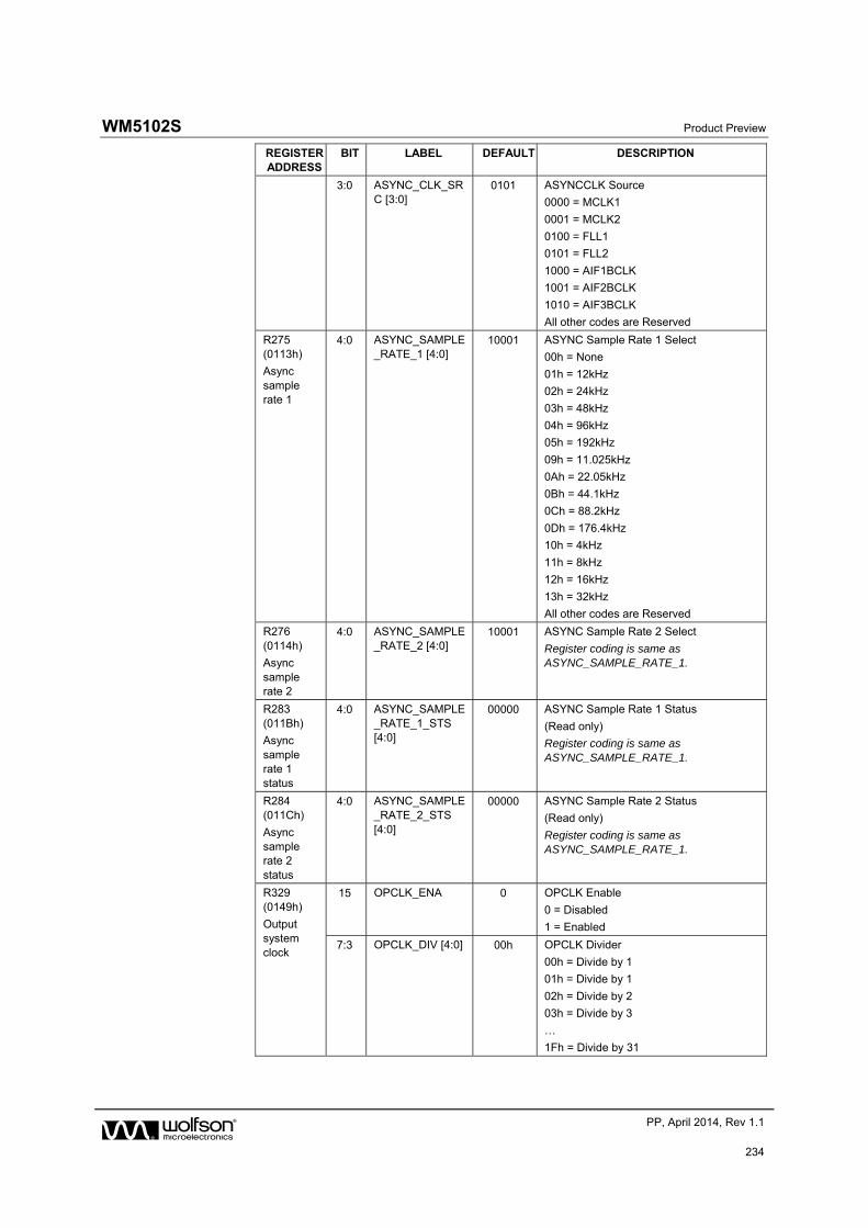
WM5102S Product Preview
w PP, April 2014, Rev 1.1
234
REGISTER ADDRESS
BIT LABEL DEFAULT DESCRIPTION
3:0 ASYNC_CLK_SRC [3:0]
0101 ASYNCCLK Source
0000 = MCLK1
0001 = MCLK2
0100 = FLL1
0101 = FLL2
1000 = AIF1BCLK
1001 = AIF2BCLK
1010 = AIF3BCLK
All other codes are Reserved
R275 (0113h)
Async sample rate 1
4:0 ASYNC_SAMPLE_RATE_1 [4:0]
10001 ASYNC Sample Rate 1 Select
00h = None
01h = 12kHz
02h = 24kHz
03h = 48kHz
04h = 96kHz
05h = 192kHz
09h = 11.025kHz
0Ah = 22.05kHz
0Bh = 44.1kHz
0Ch = 88.2kHz
0Dh = 176.4kHz
10h = 4kHz
11h = 8kHz
12h = 16kHz
13h = 32kHz
All other codes are Reserved
R276 (0114h)
Async sample rate 2
4:0 ASYNC_SAMPLE_RATE_2 [4:0]
10001 ASYNC Sample Rate 2 Select
Register coding is same as ASYNC_SAMPLE_RATE_1.
R283 (011Bh)
Async sample rate 1 status
4:0 ASYNC_SAMPLE_RATE_1_STS [4:0]
00000 ASYNC Sample Rate 1 Status
(Read only)
Register coding is same as ASYNC_SAMPLE_RATE_1.
R284 (011Ch)
Async sample rate 2 status
4:0 ASYNC_SAMPLE_RATE_2_STS [4:0]
00000 ASYNC Sample Rate 2 Status
(Read only)
Register coding is same as ASYNC_SAMPLE_RATE_1.
R329 (0149h)
Output system clock
15 OPCLK_ENA 0 OPCLK Enable
0 = Disabled
1 = Enabled
7:3 OPCLK_DIV [4:0] 00h OPCLK Divider
00h = Divide by 1
01h = Divide by 1
02h = Divide by 2
03h = Divide by 3
…
1Fh = Divide by 31
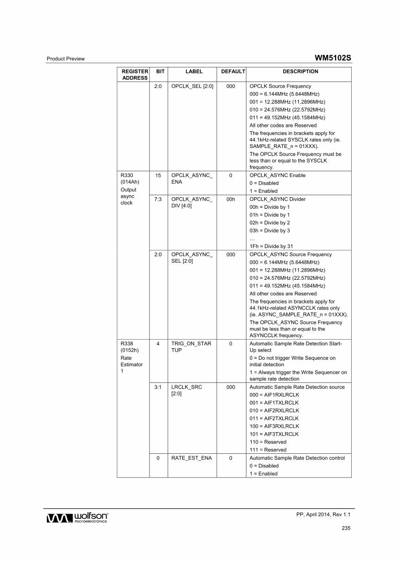
Product Preview WM5102S
w PP, April 2014, Rev 1.1
235
REGISTER ADDRESS
BIT LABEL DEFAULT DESCRIPTION
2:0 OPCLK_SEL [2:0] 000 OPCLK Source Frequency
000 = 6.144MHz (5.6448MHz)
001 = 12.288MHz (11.2896MHz)
010 = 24.576MHz (22.5792MHz)
011 = 49.152MHz (45.1584MHz)
All other codes are Reserved
The frequencies in brackets apply for 44.1kHz-related SYSCLK rates only (ie. SAMPLE_RATE_n = 01XXX).
The OPCLK Source Frequency must be less than or equal to the SYSCLK frequency.
R330 (014Ah)
Output async clock
15 OPCLK_ASYNC_ENA
0 OPCLK_ASYNC Enable
0 = Disabled
1 = Enabled
7:3 OPCLK_ASYNC_DIV [4:0]
00h OPCLK_ASYNC Divider
00h = Divide by 1
01h = Divide by 1
02h = Divide by 2
03h = Divide by 3
…
1Fh = Divide by 31
2:0 OPCLK_ASYNC_SEL [2:0]
000 OPCLK_ASYNC Source Frequency
000 = 6.144MHz (5.6448MHz)
001 = 12.288MHz (11.2896MHz)
010 = 24.576MHz (22.5792MHz)
011 = 49.152MHz (45.1584MHz)
All other codes are Reserved
The frequencies in brackets apply for 44.1kHz-related ASYNCCLK rates only (ie. ASYNC_SAMPLE_RATE_n = 01XXX).
The OPCLK_ASYNC Source Frequency must be less than or equal to the ASYNCCLK frequency.
R338 (0152h)
Rate Estimator 1
4 TRIG_ON_STARTUP
0 Automatic Sample Rate Detection Start-Up select
0 = Do not trigger Write Sequence on initial detection
1 = Always trigger the Write Sequencer on sample rate detection
3:1 LRCLK_SRC [2:0]
000 Automatic Sample Rate Detection source
000 = AIF1RXLRCLK
001 = AIF1TXLRCLK
010 = AIF2RXLRCLK
011 = AIF2TXLRCLK
100 = AIF3RXLRCLK
101 = AIF3TXLRCLK
110 = Reserved
111 = Reserved
0 RATE_EST_ENA 0 Automatic Sample Rate Detection control
0 = Disabled
1 = Enabled
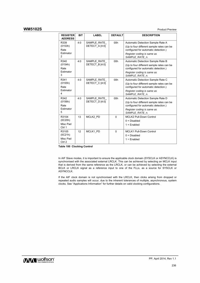
WM5102S Product Preview
w PP, April 2014, Rev 1.1
236
REGISTER ADDRESS
BIT LABEL DEFAULT DESCRIPTION
R339 (0153h)
Rate Estimator 2
4:0 SAMPLE_RATE_DETECT_A [4:0]
00h Automatic Detection Sample Rate A
(Up to four different sample rates can be configured for automatic detection.)
Register coding is same as SAMPLE_RATE_n.
R340 (0154h)
Rate Estimator 3
4:0 SAMPLE_RATE_DETECT_B [4:0]
00h Automatic Detection Sample Rate B
(Up to four different sample rates can be configured for automatic detection.)
Register coding is same as SAMPLE_RATE_n.
R341 (0155h)
Rate Estimator 4
4:0 SAMPLE_RATE_DETECT_C [4:0]
00h Automatic Detection Sample Rate C
(Up to four different sample rates can be configured for automatic detection.)
Register coding is same as SAMPLE_RATE_n.
R342 (0156h)
Rate Estimator 5
4:0 SAMPLE_RATE_DETECT_D [4:0]
00h Automatic Detection Sample Rate D
(Up to four different sample rates can be configured for automatic detection.)
Register coding is same as SAMPLE_RATE_n.
R3104 (0C20h)
Misc Pad Ctrl 1
13 MCLK2_PD 0 MCLK2 Pull-Down Control
0 = Disabled
1 = Enabled
R3105 (0C21h)
Misc Pad Ctrl 2
12 MCLK1_PD 0 MCLK1 Pull-Down Control
0 = Disabled
1 = Enabled
Table 100 Clocking Control
In AIF Slave modes, it is important to ensure the applicable clock domain (SYSCLK or ASYNCCLK) is synchronised with the associated external LRCLK. This can be achieved by selecting an MCLK input that is derived from the same reference as the LRCLK, or can be achieved by selecting the external BCLK or LRCLK signal as a reference input to one of the FLLs, as a source for SYSCLK or ASYNCCLK.
If the AIF clock domain is not synchronised with the LRCLK, then clicks arising from dropped or repeated audio samples will occur, due to the inherent tolerances of multiple, asynchronous, system clocks. See “Applications Information” for further details on valid clocking configurations.
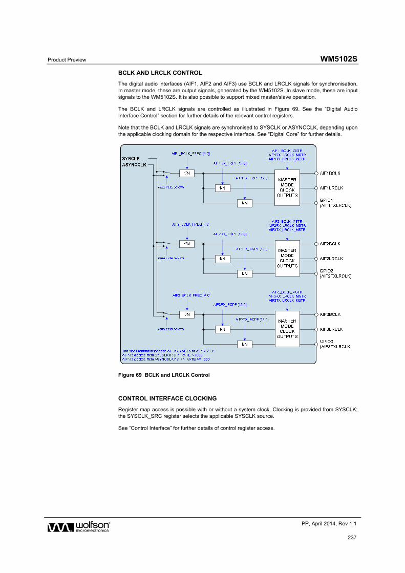
Product Preview WM5102S
w PP, April 2014, Rev 1.1
237
BCLK AND LRCLK CONTROL
The digital audio interfaces (AIF1, AIF2 and AIF3) use BCLK and LRCLK signals for synchronisation. In master mode, these are output signals, generated by the WM5102S. In slave mode, these are input signals to the WM5102S. It is also possible to support mixed master/slave operation.
The BCLK and LRCLK signals are controlled as illustrated in Figure 69. See the “Digital Audio Interface Control” section for further details of the relevant control registers.
Note that the BCLK and LRCLK signals are synchronised to SYSCLK or ASYNCCLK, depending upon the applicable clocking domain for the respective interface. See “Digital Core” for further details.
Figure 69 BCLK and LRCLK Control
CONTROL INTERFACE CLOCKING
Register map access is possible with or without a system clock. Clocking is provided from SYSCLK; the SYSCLK_SRC register selects the applicable SYSCLK source.
See “Control Interface” for further details of control register access.
WM5102S Product Preview
w PP, April 2014, Rev 1.1
238
FREQUENCY LOCKED LOOP (FLL)
Two integrated FLLs are provided to support the clocking requirements of the WM5102S. These can be enabled and configured independently according to the available reference clocks and the application requirements. The reference clock may be a high frequency (eg. 12.288MHz) or low frequency (eg. 32.768kHz).
The FLL is tolerant of jitter and may be used to generate a stable output clock from a less stable input reference. The FLL characteristics are summarised in “Electrical Characteristics”. Note that the FLL can be used to generate a free-running clock in the absence of an external reference source. This is described in the “Free-Running FLL Mode” section below. Configurable spread-spectrum modulation can be applied to the FLL outputs, to control EMI effects.
Each of the FLLs comprises two sub-systems - the ‘main’ loop and the ‘synchroniser’ loop; these can be used together to maintain best frequency accuracy and noise (jitter) performance across multiple use-cases. The two-loop design enables the FLL to synchronise effectively to an input clock that may be intermittent or noisy, whilst also achieving the performance benefits of a stable clock reference that may be asynchronous to the audio data.
The main loop takes a constant and stable clock reference as its input. For best performance, a high frequency (eg. 12.288MHz) reference is recommended. The main FLL loop will free-run without any clock reference if the input signal is removed; it can also be configured to initiate an output in the absence of any reference signal.
The synchroniser loop takes a separate clock reference as its input. The synchroniser input may be intermittent (eg. during voice calls only). The FLL uses the synchroniser input, when available, as the frequency reference. To achieve the designed performance advantage, the synchroniser input must be synchronous with the audio data.
Note that, if only a single clock input reference is used, this must be configured as the main FLL input reference. The synchroniser should be disabled in this case.
The synchroniser loop should only be used when the main loop clock reference is present. If the input reference to the main FLL is intermittent, or may be interrupted unexpectedly, then the synchroniser should be disabled.
The FLL is enabled using the FLLn_ENA register bit (where n = 1 or 2 for the corresponding FLL). The FLL Synchroniser is enabled using the FLLn_SYNC_ENA register bit.
Note that the other FLL registers should be configured before enabling the FLL; the FLLn_ENA and FLLn_SYNC_ENA register bits should be set as the final step of the FLLn enable sequence.
The FLL supports configurable free-running operation, using the FLLn_FREERUN register bits described in the next section. Note that, once the FLL output has been established, the FLL will always free-run when the input reference clock is stopped, regardless of the FLLn_FREERUN bits.
To disable the FLL while the input reference clock has stopped, the respective FLLn_FREERUN bit must be set to ‘1’, before setting the FLLn_ENA bit to ‘0’.
When changing FLL settings, it is recommended that the digital circuit be disabled via FLLn_ENA and then re-enabled after the other register settings have been updated. When changing the input reference frequency FREF, it is recommended that the FLL be reset by setting FLLn_ENA to 0.
Note that some of the FLL configuration registers can be updated while the FLL is enabled, as described below. As a general rule, however, it is recommended to configure the FLL (and FLL Synchroniser, if applicable), before setting the corresponding _ENA register bit(s).
The FLL configuration requirements are illustrated in Figure 70.
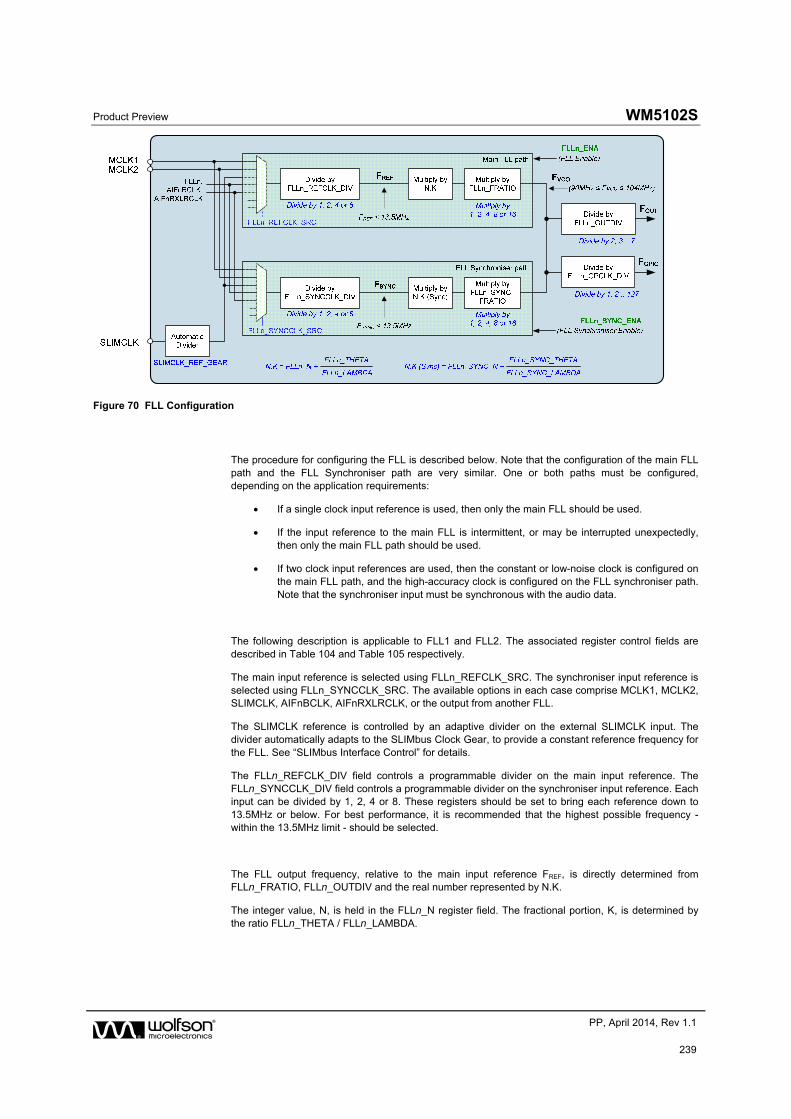
Product Preview WM5102S
w PP, April 2014, Rev 1.1
239
Figure 70 FLL Configuration
The procedure for configuring the FLL is described below. Note that the configuration of the main FLL path and the FLL Synchroniser path are very similar. One or both paths must be configured, depending on the application requirements:
If a single clock input reference is used, then only the main FLL should be used.
If the input reference to the main FLL is intermittent, or may be interrupted unexpectedly, then only the main FLL path should be used.
If two clock input references are used, then the constant or low-noise clock is configured on the main FLL path, and the high-accuracy clock is configured on the FLL synchroniser path. Note that the synchroniser input must be synchronous with the audio data.
The following description is applicable to FLL1 and FLL2. The associated register control fields are described in Table 104 and Table 105 respectively.
The main input reference is selected using FLLn_REFCLK_SRC. The synchroniser input reference is selected using FLLn_SYNCCLK_SRC. The available options in each case comprise MCLK1, MCLK2, SLIMCLK, AIFnBCLK, AIFnRXLRCLK, or the output from another FLL.
The SLIMCLK reference is controlled by an adaptive divider on the external SLIMCLK input. The divider automatically adapts to the SLIMbus Clock Gear, to provide a constant reference frequency for the FLL. See “SLIMbus Interface Control” for details.
The FLLn_REFCLK_DIV field controls a programmable divider on the main input reference. The FLLn_SYNCCLK_DIV field controls a programmable divider on the synchroniser input reference. Each input can be divided by 1, 2, 4 or 8. These registers should be set to bring each reference down to 13.5MHz or below. For best performance, it is recommended that the highest possible frequency - within the 13.5MHz limit - should be selected.
The FLL output frequency, relative to the main input reference FREF, is directly determined from FLLn_FRATIO, FLLn_OUTDIV and the real number represented by N.K.
The integer value, N, is held in the FLLn_N register field. The fractional portion, K, is determined by the ratio FLLn_THETA / FLLn_LAMBDA.
WM5102S Product Preview
w PP, April 2014, Rev 1.1
240
The FLL output frequency is generated according to the following equation:
FOUT = (FVCO / FLLn_OUTDIV)
The FLL operating frequency, FVCO is set according to the following equation:
FVCO = (FREF x N.K x FLLn_FRATIO)
FREF is the input frequency, as determined by FLLn_REFCLK_DIV.
FVCO must be in the range 90MHz to 104MHz. Frequencies outside this range cannot be supported.
Note that the output frequencies that do not lie within the ranges quoted above cannot be guaranteed across the full range of device operating conditions.
In order to follow the above requirements for FVCO, the value of FLLn_OUTDIV should be selected according to the desired output FOUT. The divider, FLLn_OUTDIV, must be set so that FVCO is in the range 90MHz to 104MHz. Supported settings of FLLn_OUTDIV are noted in Table 101.
OUTPUT FREQUENCY FOUT FLLn_OUTDIV
22.5 MHz to 26 MHz 100 (divide by 4)
45 MHz to 50 MHz 010 (divide by 2)
Table 101 Selection of FLLn_OUTDIV
The FLLn_FRATIO field selects the frequency division ratio of the FLL input. The FLLn_GAIN field is used to optimise the FLL, according to the input frequency. These fields should be set as described in Table 102.
REFERENCE FREQUENCY FREF
FLLn_FRATIO FLLn_GAIN
1MHz - 13.5MHz 0h (divide by 1) 4h (16x gain)
256kHz - 1MHz 1h (divide by 2) 2h (4x gain)
128kHz - 256kHz 2h (divide by 4) 0h (1x gain)
64kHz - 128kHz 3h (divide by 8) 0h (1x gain)
Less than 64kHz 4h (divide by 16) 0h (1x gain)
Table 102 Selection of FLLn_FRATIO and FLLn_GAIN
In order to determine the remaining FLL parameters, the FLL operating frequency, FVCO, must be calculated, as given by the following equation:
FVCO = (FOUT x FLLn_OUTDIV)
The value of N.K can then be determined as follows:
N.K = FVCO / (FLLn_FRATIO x FREF)
Note that, in the above equations:
FLLn_OUTDIV is the FOUT clock ratio.
FREF is the input frequency, after division by FLLn_REFCLK_DIV, where applicable.
FLLn_FRATIO is the FVCO clock ratio (1, 2, 4, 8 or 16).
Product Preview WM5102S
w PP, April 2014, Rev 1.1
241
The value of N is held in the FLLn_N register field.
The value of K is determined by the ratio FLLn_THETA / FLLn_LAMBDA.
The FLLn_N, FLLn_THETA and FLLn_LAMBDA fields are all coded as integers (LSB = 1).
If the FLLn_N or FLLn_THETA registers are updated while the FLL is enabled (FLLn_ENA=1), then the new values will only be effective when a ‘1’ is written to the FLLn_CTRL_UPD bit. This makes it possible to update the two registers simultaneously, without disabling the FLL.
Note that, when the FLL is disabled (FLLn_ENA=0), then the FLLn_N and FLLn_THETA registers can be updated without writing to the FLLn_CTRL_UPD bit.
The values of FLLn_THETA and FLLn_LAMBDA can be calculated as described later.
A similar procedure applies for the deriviation of the FLL Synchroniser parameters - assuming that this function is used.
The FLLn_SYNC_FRATIO field selects the frequency division ratio of the FLL synchroniser input. The FLLn_GAIN and FLLn_SYNC_DFSAT fields are used to optimise the FLL, according to the input frequency. These fields should be set as described in Table 103.
SYNCHRONISER FREQUENCY FSYNC
FLLn_SYNC_FRATIO FLLn_SYNC_GAIN FLLn_SYNC_DFSAT
1MHz - 13.5MHz 0h (divide by 1) 4h (16x gain) 0 (wide bandwidth)
256kHz - 1MHz 1h (divide by 2) 2h (4x gain) 0 (wide bandwidth)
128kHz - 256kHz 2h (divide by 4) 0h (1x gain) 0 (wide bandwidth)
64kHz - 128kHz 3h (divide by 8) 0h (1x gain) 1 (narrow bandwidth)
Less than 64kHz 4h (divide by 16) 0h (1x gain) 1 (narrow bandwidth)
Table 103 Selection of FLLn_SYNC_FRATIO, FLLn_SYNC_GAIN, FLLn_SYNC_DFSAT
The FLL operating frequency, FVCO, is the same frequency calculated as described above.
The value of N.K (Sync) can then be determined as follows:
N.K (Sync) = FVCO / (FLLn_SYNC_FRATIO x FSYNC)
Note that, in the above equations:
FSYNC is the synchroniser input frequency, after division by FLLn_SYNCCLK_DIV, where applicable.
FLLn_SYNC_FRATIO is the FVCO clock ratio (1, 2, 4, 8 or 16).
The value of N (Sync) is held in the FLLn_SYNC_N register field.
The value of K (Sync) is determined by the ratio FLLn_SYNC_THETA / FLLn_SYNC_LAMBDA.
The FLLn_SYNC_N, FLLn_SYNC_THETA and FLLn_SYNC_LAMBDA fields are all coded as integers (LSB = 1).
WM5102S Product Preview
w PP, April 2014, Rev 1.1
242
In Fractional Mode (FLLn_THETA > 0), the register fields FLLn_THETA and FLLn_LAMBDA can be calculated as described below.
Note that an equivalent procedure is also used to derive the FLLn_SYNC_THETA and FLLn_SYNC_LAMBDA register values from the corresponding synchroniser parameters.
Calculate GCD(FLL) using the ‘Greatest Common Denominator’ function:
GCD(FLL) = GCD(FLLn_FRATIO x FREF, FVCO)
where GCD(x, y) is the greatest common denominator of x and y
FREF is the input frequency, after division by FLLn_REFCLK_DIV, where applicable.
Next, calculate FLLn_THETA and FLLn_LAMBDA using the following equations:
FLLn_THETA = (FVCO - (FLL_N x FLLn_FRATIO x FREF)) / GCD(FLL)
FLLn_LAMBDA = (FLLn_FRATIO x FREF) / GCD(FLL)
Note that, in Fractional Mode, the values of FLLn_THETA and FLLn_LAMBDA must be co-prime (ie. not divisible by any common integer). The calculation above ensures that the values will be co-prime.
The value of K must be a fraction less than 1 (ie. FLLn_THETA must be less than FLLn_LAMBDA).
The FLL control registers are described in Table 104 and Table 105. Example settings for a variety of reference frequencies and output frequencies are shown in Table 108.
REGISTER ADDRESS
BIT LABEL DEFAULT DESCRIPTION
R369 (0171h)
FLL1 Control 1
0 FLL1_ENA 0 FLL1 Enable
0 = Disabled
1 = Enabled
This should be set as the final step of the FLL1 enable sequence, ie. after the other FLL registers have been configured.
R370 (0172h)
FLL1 Control 2
15 FLL1_CTRL_UPD
0 FLL1 Control Update
Write ‘1’ to apply the FLL1_N and FLL1_THETA register settings.
(Only valid when FLL1_ENA=1)
9:0 FLL1_N [9:0] 008h FLL1 Integer multiply for FREF
(LSB = 1)
If updated while the FLL is enabled, the new value is only effective when a ‘1’ is written to FLL1_CTRL_UPD.
R371 (0173h)
FLL1 Control 3
15:0 FLL1_THETA [15:0]
0018h FLL1 Fractional multiply for FREF
This field sets the numerator (multiply) part of the FLL1_THETA / FLL1_LAMBDA ratio.
Coded as LSB = 1.
If updated while the FLL is enabled, the new value is only effective when a ‘1’ is written to FLL1_CTRL_UPD.
R372 (0174h)
FLL1 Control 4
15:0 FLL1_LAMBDA [15:0]
007Dh FLL1 Fractional multiply for FREF
This field sets the denominator (dividing) part of the FLL1_THETA / FLL1_LAMBDA ratio.
Coded as LSB = 1.
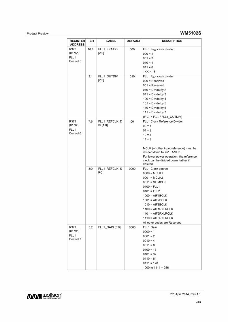
Product Preview WM5102S
w PP, April 2014, Rev 1.1
243
REGISTER ADDRESS
BIT LABEL DEFAULT DESCRIPTION
R373 (0175h)
FLL1 Control 5
10:8 FLL1_FRATIO [2:0]
000 FLL1 FVCO clock divider
000 = 1
001 = 2
010 = 4
011 = 8
1XX = 16
3:1 FLL1_OUTDIV [2:0]
010 FLL1 FOUT clock divider
000 = Reserved
001 = Reserved
010 = Divide by 2
011 = Divide by 3
100 = Divide by 4
101 = Divide by 5
110 = Divide by 6
111 = Divide by 7
(FOUT = FVCO / FLL1_OUTDIV)
R374 (0176h)
FLL1 Control 6
7:6 FLL1_REFCLK_DIV [1:0]
00 FLL1 Clock Reference Divider
00 = 1
01 = 2
10 = 4
11 = 8
MCLK (or other input reference) must be divided down to <=13.5MHz.
For lower power operation, the reference clock can be divided down further if desired.
3:0 FLL1_REFCLK_SRC
0000 FLL1 Clock source
0000 = MCLK1
0001 = MCLK2
0011 = SLIMCLK
0100 = FLL1
0101 = FLL2
1000 = AIF1BCLK
1001 = AIF2BCLK
1010 = AIF3BCLK
1100 = AIF1RXLRCLK
1101 = AIF2RXLRCLK
1110 = AIF3RXLRCLK
All other codes are Reserved
R377 (0179h)
FLL1 Control 7
5:2 FLL1_GAIN [3:0] 0000 FLL1 Gain
0000 = 1
0001 = 2
0010 = 4
0011 = 8
0100 = 16
0101 = 32
0110 = 64
0111 = 128
1000 to 1111 = 256
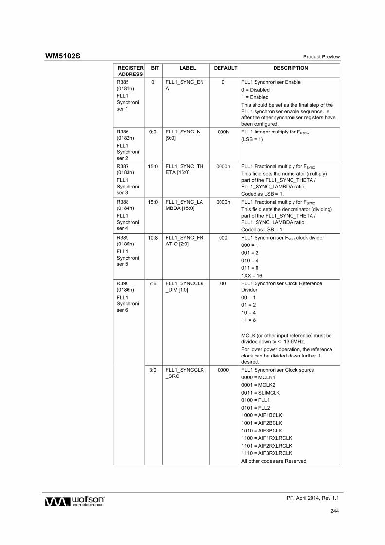
WM5102S Product Preview
w PP, April 2014, Rev 1.1
244
REGISTER ADDRESS
BIT LABEL DEFAULT DESCRIPTION
R385 (0181h)
FLL1 Synchroniser 1
0 FLL1_SYNC_ENA
0 FLL1 Synchroniser Enable
0 = Disabled
1 = Enabled
This should be set as the final step of the FLL1 synchroniser enable sequence, ie. after the other synchroniser registers have been configured.
R386 (0182h)
FLL1 Synchroniser 2
9:0 FLL1_SYNC_N [9:0]
000h FLL1 Integer multiply for FSYNC
(LSB = 1)
R387 (0183h)
FLL1 Synchroniser 3
15:0 FLL1_SYNC_THETA [15:0]
0000h FLL1 Fractional multiply for FSYNC
This field sets the numerator (multiply) part of the FLL1_SYNC_THETA / FLL1_SYNC_LAMBDA ratio.
Coded as LSB = 1.
R388 (0184h)
FLL1 Synchroniser 4
15:0 FLL1_SYNC_LAMBDA [15:0]
0000h FLL1 Fractional multiply for FSYNC
This field sets the denominator (dividing) part of the FLL1_SYNC_THETA / FLL1_SYNC_LAMBDA ratio.
Coded as LSB = 1.
R389 (0185h)
FLL1 Synchroniser 5
10:8 FLL1_SYNC_FRATIO [2:0]
000 FLL1 Synchroniser FVCO clock divider
000 = 1
001 = 2
010 = 4
011 = 8
1XX = 16
R390 (0186h)
FLL1 Synchroniser 6
7:6 FLL1_SYNCCLK_DIV [1:0]
00 FLL1 Synchroniser Clock Reference Divider
00 = 1
01 = 2
10 = 4
11 = 8
MCLK (or other input reference) must be divided down to <=13.5MHz.
For lower power operation, the reference clock can be divided down further if desired.
3:0 FLL1_SYNCCLK_SRC
0000 FLL1 Synchroniser Clock source
0000 = MCLK1
0001 = MCLK2
0011 = SLIMCLK
0100 = FLL1
0101 = FLL2
1000 = AIF1BCLK
1001 = AIF2BCLK
1010 = AIF3BCLK
1100 = AIF1RXLRCLK
1101 = AIF2RXLRCLK
1110 = AIF3RXLRCLK
All other codes are Reserved
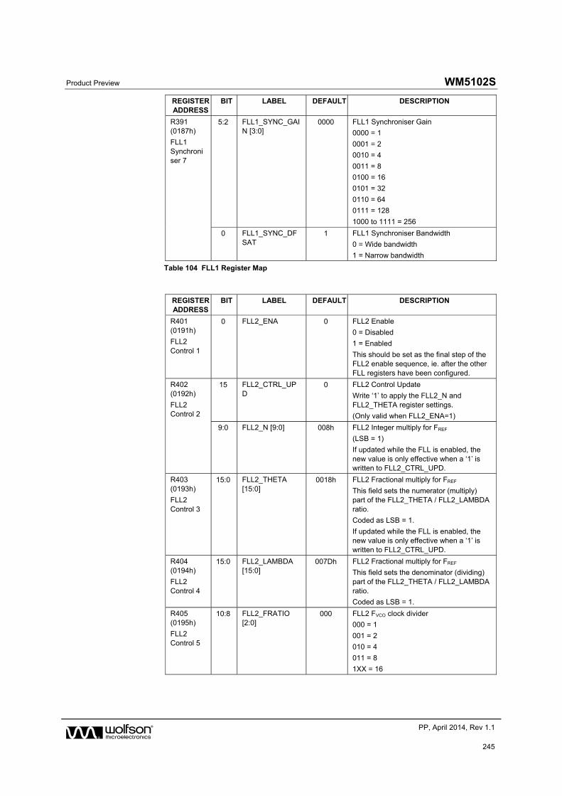
Product Preview WM5102S
w PP, April 2014, Rev 1.1
245
REGISTER ADDRESS
BIT LABEL DEFAULT DESCRIPTION
R391 (0187h)
FLL1 Synchroniser 7
5:2 FLL1_SYNC_GAIN [3:0]
0000 FLL1 Synchroniser Gain
0000 = 1
0001 = 2
0010 = 4
0011 = 8
0100 = 16
0101 = 32
0110 = 64
0111 = 128
1000 to 1111 = 256
0 FLL1_SYNC_DFSAT
1 FLL1 Synchroniser Bandwidth
0 = Wide bandwidth
1 = Narrow bandwidth
Table 104 FLL1 Register Map
REGISTER ADDRESS
BIT LABEL DEFAULT DESCRIPTION
R401 (0191h)
FLL2 Control 1
0 FLL2_ENA 0 FLL2 Enable
0 = Disabled
1 = Enabled
This should be set as the final step of the FLL2 enable sequence, ie. after the other FLL registers have been configured.
R402 (0192h)
FLL2 Control 2
15 FLL2_CTRL_UPD
0 FLL2 Control Update
Write ‘1’ to apply the FLL2_N and FLL2_THETA register settings.
(Only valid when FLL2_ENA=1)
9:0 FLL2_N [9:0] 008h FLL2 Integer multiply for FREF
(LSB = 1)
If updated while the FLL is enabled, the new value is only effective when a ‘1’ is written to FLL2_CTRL_UPD.
R403 (0193h)
FLL2 Control 3
15:0 FLL2_THETA [15:0]
0018h FLL2 Fractional multiply for FREF
This field sets the numerator (multiply) part of the FLL2_THETA / FLL2_LAMBDA ratio.
Coded as LSB = 1.
If updated while the FLL is enabled, the new value is only effective when a ‘1’ is written to FLL2_CTRL_UPD.
R404 (0194h)
FLL2 Control 4
15:0 FLL2_LAMBDA [15:0]
007Dh FLL2 Fractional multiply for FREF
This field sets the denominator (dividing) part of the FLL2_THETA / FLL2_LAMBDA ratio.
Coded as LSB = 1.
R405 (0195h)
FLL2 Control 5
10:8 FLL2_FRATIO [2:0]
000 FLL2 FVCO clock divider
000 = 1
001 = 2
010 = 4
011 = 8
1XX = 16
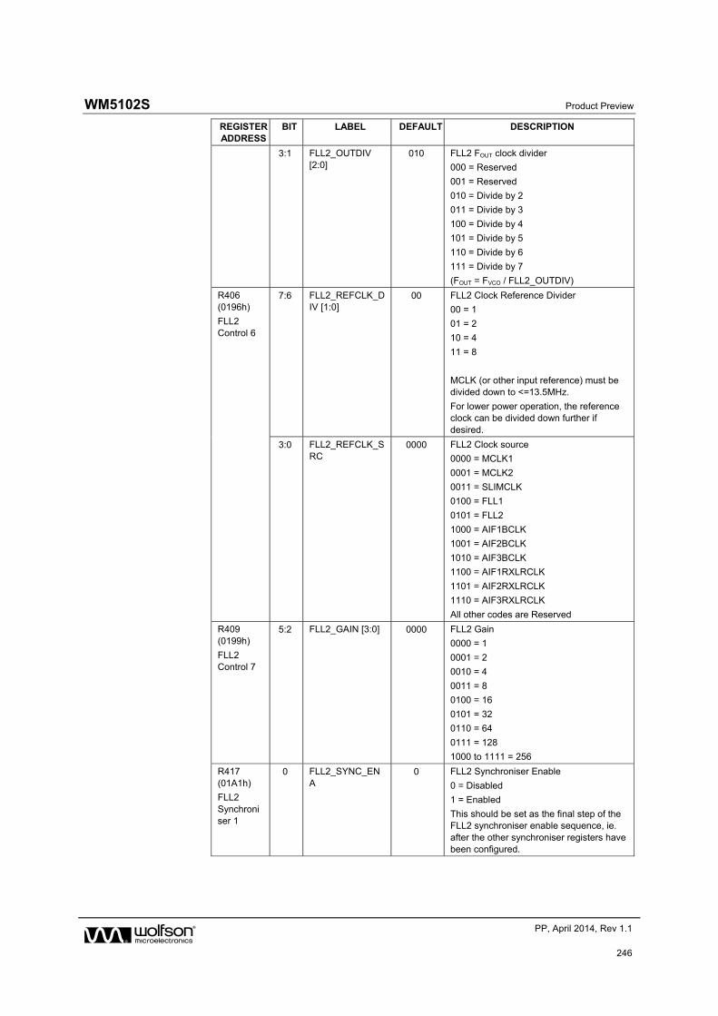
WM5102S Product Preview
w PP, April 2014, Rev 1.1
246
REGISTER ADDRESS
BIT LABEL DEFAULT DESCRIPTION
3:1 FLL2_OUTDIV [2:0]
010 FLL2 FOUT clock divider
000 = Reserved
001 = Reserved
010 = Divide by 2
011 = Divide by 3
100 = Divide by 4
101 = Divide by 5
110 = Divide by 6
111 = Divide by 7
(FOUT = FVCO / FLL2_OUTDIV)
R406 (0196h)
FLL2 Control 6
7:6 FLL2_REFCLK_DIV [1:0]
00 FLL2 Clock Reference Divider
00 = 1
01 = 2
10 = 4
11 = 8
MCLK (or other input reference) must be divided down to <=13.5MHz.
For lower power operation, the reference clock can be divided down further if desired.
3:0 FLL2_REFCLK_SRC
0000 FLL2 Clock source
0000 = MCLK1
0001 = MCLK2
0011 = SLIMCLK
0100 = FLL1
0101 = FLL2
1000 = AIF1BCLK
1001 = AIF2BCLK
1010 = AIF3BCLK
1100 = AIF1RXLRCLK
1101 = AIF2RXLRCLK
1110 = AIF3RXLRCLK
All other codes are Reserved
R409 (0199h)
FLL2 Control 7
5:2 FLL2_GAIN [3:0] 0000 FLL2 Gain
0000 = 1
0001 = 2
0010 = 4
0011 = 8
0100 = 16
0101 = 32
0110 = 64
0111 = 128
1000 to 1111 = 256
R417 (01A1h)
FLL2 Synchroniser 1
0 FLL2_SYNC_ENA
0 FLL2 Synchroniser Enable
0 = Disabled
1 = Enabled
This should be set as the final step of the FLL2 synchroniser enable sequence, ie. after the other synchroniser registers have been configured.
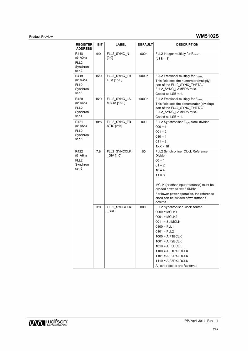
Product Preview WM5102S
w PP, April 2014, Rev 1.1
247
REGISTER ADDRESS
BIT LABEL DEFAULT DESCRIPTION
R418 (01A2h)
FLL2 Synchroniser 2
9:0 FLL2_SYNC_N [9:0]
000h FLL2 Integer multiply for FSYNC
(LSB = 1)
R419 (01A3h)
FLL2 Synchroniser 3
15:0 FLL2_SYNC_THETA [15:0]
0000h FLL2 Fractional multiply for FSYNC
This field sets the numerator (multiply) part of the FLL2_SYNC_THETA / FLL2_SYNC_LAMBDA ratio.
Coded as LSB = 1.
R420 (01A4h)
FLL2 Synchroniser 4
15:0 FLL2_SYNC_LAMBDA [15:0]
0000h FLL2 Fractional multiply for FSYNC
This field sets the denominator (dividing) part of the FLL2_SYNC_THETA / FLL2_SYNC_LAMBDA ratio.
Coded as LSB = 1.
R421 (01A5h)
FLL2 Synchroniser 5
10:8 FLL2_SYNC_FRATIO [2:0]
000 FLL2 Synchroniser FVCO clock divider
000 = 1
001 = 2
010 = 4
011 = 8
1XX = 16
R422 (01A6h)
FLL2 Synchroniser 6
7:6 FLL2_SYNCCLK_DIV [1:0]
00 FLL2 Synchroniser Clock Reference Divider
00 = 1
01 = 2
10 = 4
11 = 8
MCLK (or other input reference) must be divided down to <=13.5MHz.
For lower power operation, the reference clock can be divided down further if desired.
3:0 FLL2_SYNCCLK_SRC
0000 FLL2 Synchroniser Clock source
0000 = MCLK1
0001 = MCLK2
0011 = SLIMCLK
0100 = FLL1
0101 = FLL2
1000 = AIF1BCLK
1001 = AIF2BCLK
1010 = AIF3BCLK
1100 = AIF1RXLRCLK
1101 = AIF2RXLRCLK
1110 = AIF3RXLRCLK
All other codes are Reserved
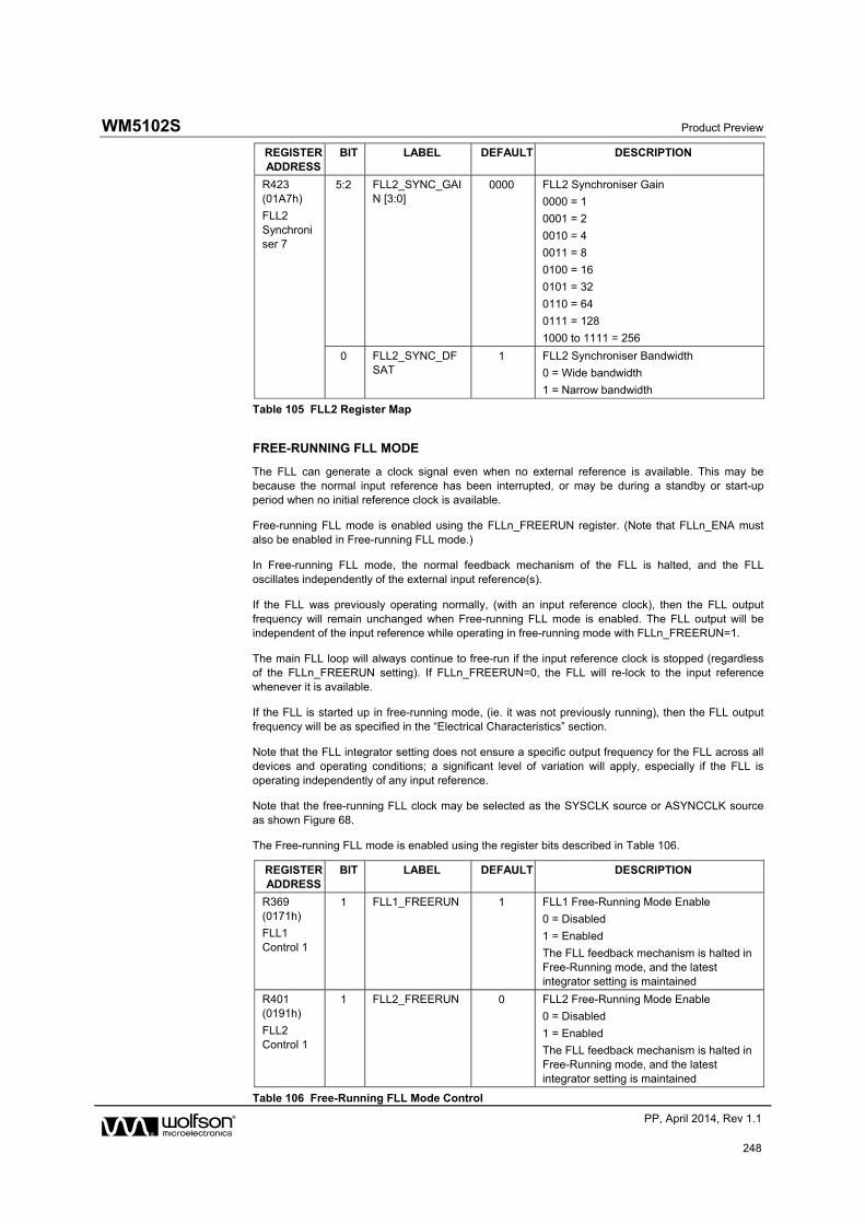
WM5102S Product Preview
w PP, April 2014, Rev 1.1
248
REGISTER ADDRESS
BIT LABEL DEFAULT DESCRIPTION
R423 (01A7h)
FLL2 Synchroniser 7
5:2 FLL2_SYNC_GAIN [3:0]
0000 FLL2 Synchroniser Gain
0000 = 1
0001 = 2
0010 = 4
0011 = 8
0100 = 16
0101 = 32
0110 = 64
0111 = 128
1000 to 1111 = 256
0 FLL2_SYNC_DFSAT
1 FLL2 Synchroniser Bandwidth
0 = Wide bandwidth
1 = Narrow bandwidth
Table 105 FLL2 Register Map
FREE-RUNNING FLL MODE
The FLL can generate a clock signal even when no external reference is available. This may be because the normal input reference has been interrupted, or may be during a standby or start-up period when no initial reference clock is available.
Free-running FLL mode is enabled using the FLLn_FREERUN register. (Note that FLLn_ENA must also be enabled in Free-running FLL mode.)
In Free-running FLL mode, the normal feedback mechanism of the FLL is halted, and the FLL oscillates independently of the external input reference(s).
If the FLL was previously operating normally, (with an input reference clock), then the FLL output frequency will remain unchanged when Free-running FLL mode is enabled. The FLL output will be independent of the input reference while operating in free-running mode with FLLn_FREERUN=1.
The main FLL loop will always continue to free-run if the input reference clock is stopped (regardless of the FLLn_FREERUN setting). If FLLn_FREERUN=0, the FLL will re-lock to the input reference whenever it is available.
If the FLL is started up in free-running mode, (ie. it was not previously running), then the FLL output frequency will be as specified in the “Electrical Characteristics” section.
Note that the FLL integrator setting does not ensure a specific output frequency for the FLL across all devices and operating conditions; a significant level of variation will apply, especially if the FLL is operating independently of any input reference.
Note that the free-running FLL clock may be selected as the SYSCLK source or ASYNCCLK source as shown Figure 68.
The Free-running FLL mode is enabled using the register bits described in Table 106.
REGISTER ADDRESS
BIT LABEL DEFAULT DESCRIPTION
R369 (0171h)
FLL1 Control 1
1 FLL1_FREERUN 1 FLL1 Free-Running Mode Enable
0 = Disabled
1 = Enabled
The FLL feedback mechanism is halted in Free-Running mode, and the latest integrator setting is maintained
R401 (0191h)
FLL2 Control 1
1 FLL2_FREERUN 0 FLL2 Free-Running Mode Enable
0 = Disabled
1 = Enabled
The FLL feedback mechanism is halted in Free-Running mode, and the latest integrator setting is maintained
Table 106 Free-Running FLL Mode Control
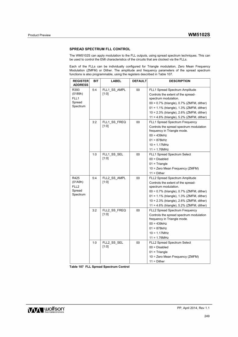
Product Preview WM5102S
w PP, April 2014, Rev 1.1
249
SPREAD SPECTRUM FLL CONTROL
The WM5102S can apply modulation to the FLL outputs, using spread spectrum techniques. This can be used to control the EMI characteristics of the circuits that are clocked via the FLLs.
Each of the FLLs can be individually configured for Triangle modulation, Zero Mean Frequency Modulation (ZMFM) or Dither. The amplitude and frequency parameters of the spread spectrum functions is also programmable, using the registers described in Table 107.
REGISTER ADDRESS
BIT LABEL DEFAULT DESCRIPTION
R393 (0189h)
FLL1 Spread Spectrum
5:4 FLL1_SS_AMPL [1:0]
00 FLL1 Spread Spectrum Amplitude
Controls the extent of the spread-spectrum modulation.
00 = 0.7% (triangle), 0.7% (ZMFM, dither)
01 = 1.1% (triangle), 1.3% (ZMFM, dither)
10 = 2.3% (triangle), 2.6% (ZMFM, dither)
11 = 4.6% (triangle), 5.2% (ZMFM, dither)
3:2 FLL1_SS_FREQ [1:0]
00 FLL1 Spread Spectrum Frequency
Controls the spread spectrum modulation frequency in Triangle mode.
00 = 439kHz
01 = 878kHz
10 = 1.17MHz
11 = 1.76MHz
1:0 FLL1_SS_SEL [1:0]
00 FLL1 Spread Spectrum Select
00 = Disabled
01 = Triangle
10 = Zero Mean Frequency (ZMFM)
11 = Dither
R425 (01A9h)
FLL2 Spread Spectrum
5:4 FLL2_SS_AMPL [1:0]
00 FLL2 Spread Spectrum Amplitude
Controls the extent of the spread-spectrum modulation.
00 = 0.7% (triangle), 0.7% (ZMFM, dither)
01 = 1.1% (triangle), 1.3% (ZMFM, dither)
10 = 2.3% (triangle), 2.6% (ZMFM, dither)
11 = 4.6% (triangle), 5.2% (ZMFM, dither)
3:2 FLL2_SS_FREQ [1:0]
00 FLL2 Spread Spectrum Frequency
Controls the spread spectrum modulation frequency in Triangle mode.
00 = 439kHz
01 = 878kHz
10 = 1.17MHz
11 = 1.76MHz
1:0 FLL2_SS_SEL [1:0]
00 FLL2 Spread Spectrum Select
00 = Disabled
01 = Triangle
10 = Zero Mean Frequency (ZMFM)
11 = Dither
Table 107 FLL Spread Spectrum Control
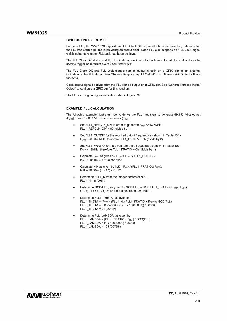
WM5102S Product Preview
w PP, April 2014, Rev 1.1
250
GPIO OUTPUTS FROM FLL
For each FLL, the WM5102S supports an ‘FLL Clock OK’ signal which, when asserted, indicates that the FLL has started up and is providing an output clock. Each FLL also supports an ‘FLL Lock’ signal which indicates whether FLL Lock has been achieved.
The FLL Clock OK status and FLL Lock status are inputs to the Interrupt control circuit and can be used to trigger an Interrupt event - see “Interrupts”.
The FLL Clock OK and FLL Lock signals can be output directly on a GPIO pin as an external indication of the FLL status. See “General Purpose Input / Output” to configure a GPIO pin for these functions.
Clock output signals derived from the FLL can be output on a GPIO pin. See “General Purpose Input / Output” to configure a GPIO pin for this function.
The FLL clocking configuration is illustrated in Figure 70.
EXAMPLE FLL CALCULATION
The following example illustrates how to derive the FLL1 registers to generate 49.152 MHz output (FOUT) from a 12.000 MHz reference clock (FREF):
Set FLL1_REFCLK_DIV in order to generate FREF <=13.5MHz: FLL1_REFCLK_DIV = 00 (divide by 1)
Set FLL1_OUTDIV for the required output frequency as shown in Table 101:- FOUT = 49.152 MHz, therefore FLL1_OUTDIV = 2h (divide by 2)
Set FLL1_FRATIO for the given reference frequency as shown in Table 102: FREF = 12MHz, therefore FLL1_FRATIO = 0h (divide by 1)
Calculate FVCO as given by FVCO = FOUT x FLL1_OUTDIV:- FVCO = 49.152 x 2 = 98.304MHz
Calculate N.K as given by N.K = FVCO / (FLL1_FRATIO x FREF): N.K = 98.304 / (1 x 12) = 8.192
Determine FLL1_N from the integer portion of N.K:- FLL1_N = 8 (008h)
Determine GCD(FLL), as given by GCD(FLL) = GCD(FLL1_FRATIO x FREF, FVCO): GCD(FLL) = GCD(1 x 12000000, 98304000) = 96000
Determine FLL1_THETA, as given by FLL1_THETA = (FVCO - (FLL1_N x FLL1_FRATIO x FREF)) / GCD(FLL): FLL1_THETA = (98304000 - (8 x 1 x 12000000)) / 96000 FLL1_THETA = 24 (0018h)
Determine FLL_LAMBDA, as given by FLL1_LAMBDA = (FLL1_FRATIO x FREF) / GCD(FLL): FLL1_LAMBDA = (1 x 12000000) / 96000 FLL1_LAMBDA = 125 (007Dh)
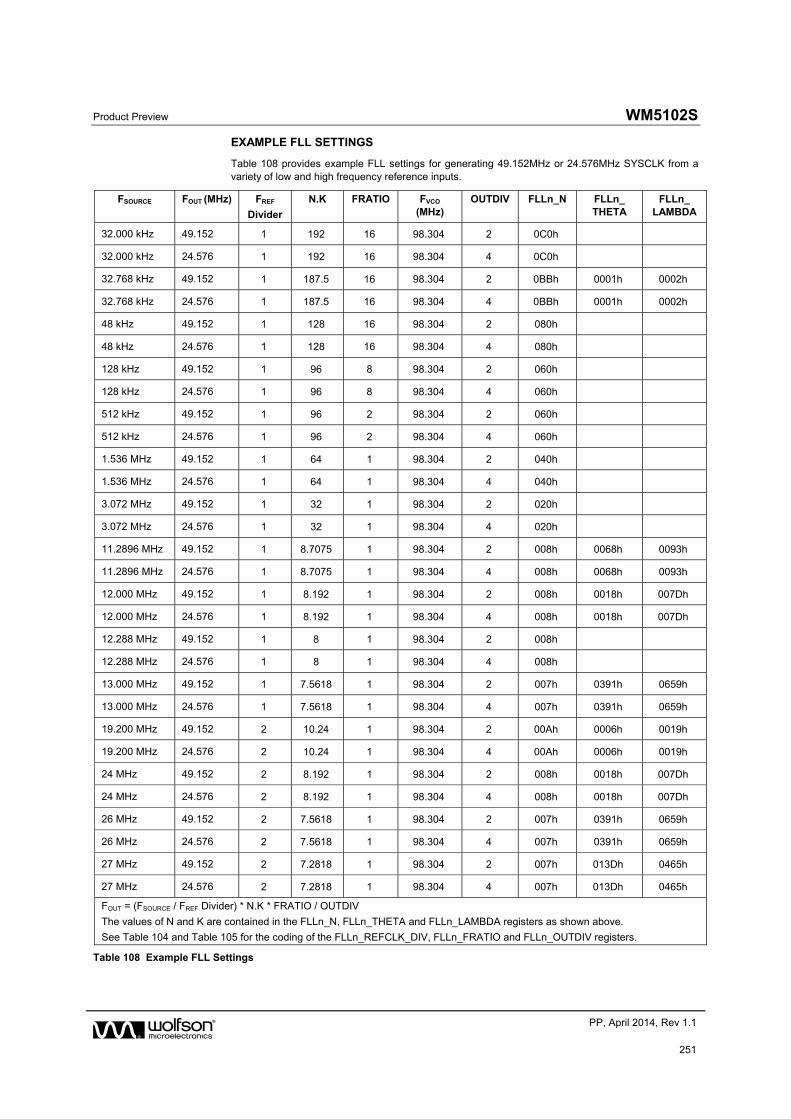
Product Preview WM5102S
w PP, April 2014, Rev 1.1
251
EXAMPLE FLL SETTINGS
Table 108 provides example FLL settings for generating 49.152MHz or 24.576MHz SYSCLK from a variety of low and high frequency reference inputs.
FSOURCE FOUT (MHz) FREF
Divider
N.K FRATIO FVCO
(MHz) OUTDIV FLLn_N FLLn_
THETA FLLn_
LAMBDA
32.000 kHz 49.152 1 192 16 98.304 2 0C0h
32.000 kHz 24.576 1 192 16 98.304 4 0C0h
32.768 kHz 49.152 1 187.5 16 98.304 2 0BBh 0001h 0002h
32.768 kHz 24.576 1 187.5 16 98.304 4 0BBh 0001h 0002h
48 kHz 49.152 1 128 16 98.304 2 080h
48 kHz 24.576 1 128 16 98.304 4 080h
128 kHz 49.152 1 96 8 98.304 2 060h
128 kHz 24.576 1 96 8 98.304 4 060h
512 kHz 49.152 1 96 2 98.304 2 060h
512 kHz 24.576 1 96 2 98.304 4 060h
1.536 MHz 49.152 1 64 1 98.304 2 040h
1.536 MHz 24.576 1 64 1 98.304 4 040h
3.072 MHz 49.152 1 32 1 98.304 2 020h
3.072 MHz 24.576 1 32 1 98.304 4 020h
11.2896 MHz 49.152 1 8.7075 1 98.304 2 008h 0068h 0093h
11.2896 MHz 24.576 1 8.7075 1 98.304 4 008h 0068h 0093h
12.000 MHz 49.152 1 8.192 1 98.304 2 008h 0018h 007Dh
12.000 MHz 24.576 1 8.192 1 98.304 4 008h 0018h 007Dh
12.288 MHz 49.152 1 8 1 98.304 2 008h
12.288 MHz 24.576 1 8 1 98.304 4 008h
13.000 MHz 49.152 1 7.5618 1 98.304 2 007h 0391h 0659h
13.000 MHz 24.576 1 7.5618 1 98.304 4 007h 0391h 0659h
19.200 MHz 49.152 2 10.24 1 98.304 2 00Ah 0006h 0019h
19.200 MHz 24.576 2 10.24 1 98.304 4 00Ah 0006h 0019h
24 MHz 49.152 2 8.192 1 98.304 2 008h 0018h 007Dh
24 MHz 24.576 2 8.192 1 98.304 4 008h 0018h 007Dh
26 MHz 49.152 2 7.5618 1 98.304 2 007h 0391h 0659h
26 MHz 24.576 2 7.5618 1 98.304 4 007h 0391h 0659h
27 MHz 49.152 2 7.2818 1 98.304 2 007h 013Dh 0465h
27 MHz 24.576 2 7.2818 1 98.304 4 007h 013Dh 0465h
FOUT = (FSOURCE / FREF Divider) * N.K * FRATIO / OUTDIV
The values of N and K are contained in the FLLn_N, FLLn_THETA and FLLn_LAMBDA registers as shown above.
See Table 104 and Table 105 for the coding of the FLLn_REFCLK_DIV, FLLn_FRATIO and FLLn_OUTDIV registers.
Table 108 Example FLL Settings
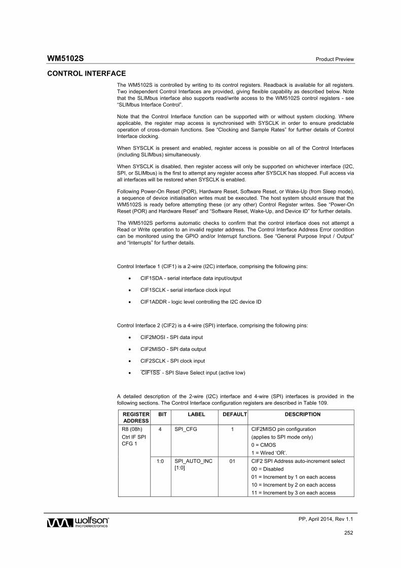
WM5102S Product Preview
w PP, April 2014, Rev 1.1
252
CONTROL INTERFACE
The WM5102S is controlled by writing to its control registers. Readback is available for all registers. Two independent Control Interfaces are provided, giving flexible capability as described below. Note that the SLIMbus interface also supports read/write access to the WM5102S control registers - see “SLIMbus Interface Control”.
Note that the Control Interface function can be supported with or without system clocking. Where applicable, the register map access is synchronised with SYSCLK in order to ensure predictable operation of cross-domain functions. See “Clocking and Sample Rates” for further details of Control Interface clocking.
When SYSCLK is present and enabled, register access is possible on all of the Control Interfaces (including SLIMbus) simultaneously.
When SYSCLK is disabled, then register access will only be supported on whichever interface (I2C, SPI, or SLIMbus) is the first to attempt any register access after SYSCLK has stopped. Full access via all interfaces will be restored when SYSCLK is enabled.
Following Power-On Reset (POR), Hardware Reset, Software Reset, or Wake-Up (from Sleep mode), a sequence of device initialisation writes must be executed. The host system should ensure that the WM5102S is ready before attempting these (or any other) Control Register writes. See “Power-On Reset (POR) and Hardware Reset” and “Software Reset, Wake-Up, and Device ID” for further details.
The WM5102S performs automatic checks to confirm that the control interface does not attempt a Read or Write operation to an invalid register address. The Control Interface Address Error condition can be monitored using the GPIO and/or Interrupt functions. See “General Purpose Input / Output” and “Interrupts” for further details.
Control Interface 1 (CIF1) is a 2-wire (I2C) interface, comprising the following pins:
CIF1SDA - serial interface data input/output
CIF1SCLK - serial interface clock input
CIF1ADDR - logic level controlling the I2C device ID
Control Interface 2 (CIF2) is a 4-wire (SPI) interface, comprising the following pins:
CIF2MOSI - SPI data input
CIF2MISO - SPI data output
CIF2SCLK - SPI clock input
CIF1SS¯¯¯¯¯¯¯ - SPI Slave Select input (active low)
A detailed description of the 2-wire (I2C) interface and 4-wire (SPI) interfaces is provided in the following sections. The Control Interface configuration registers are described in Table 109.
REGISTER ADDRESS
BIT LABEL DEFAULT DESCRIPTION
R8 (08h)
Ctrl IF SPI CFG 1
4 SPI_CFG 1 CIF2MISO pin configuration
(applies to SPI mode only)
0 = CMOS
1 = Wired ‘OR’.
1:0 SPI_AUTO_INC [1:0]
01 CIF2 SPI Address auto-increment select
00 = Disabled
01 = Increment by 1 on each access
10 = Increment by 2 on each access
11 = Increment by 3 on each access
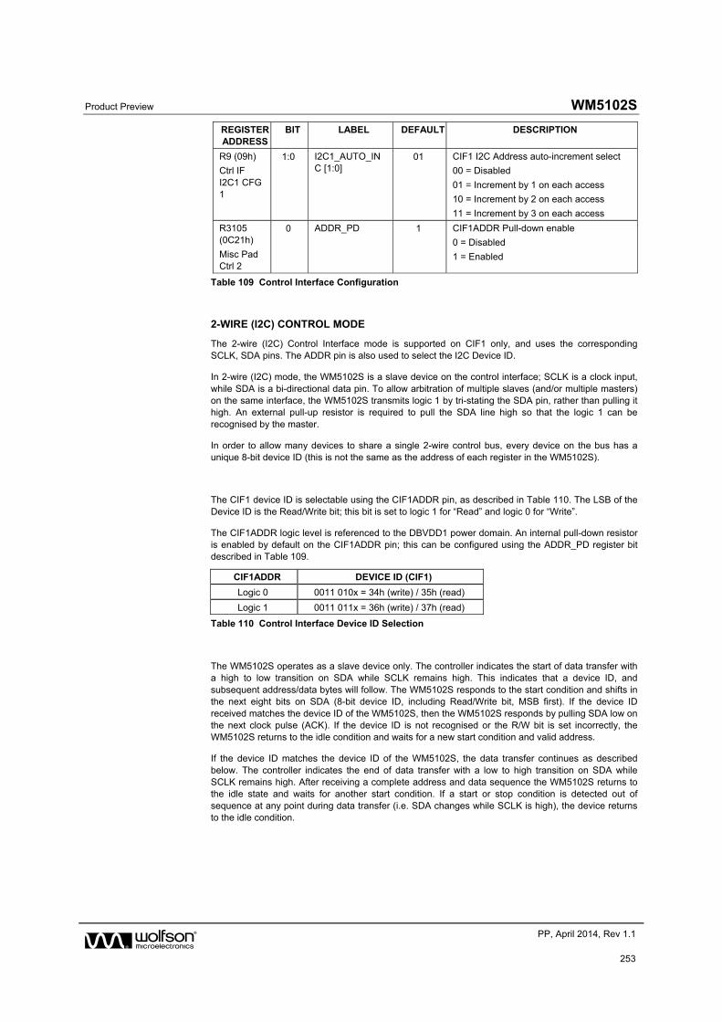
Product Preview WM5102S
w PP, April 2014, Rev 1.1
253
REGISTER ADDRESS
BIT LABEL DEFAULT DESCRIPTION
R9 (09h)
Ctrl IF I2C1 CFG 1
1:0 I2C1_AUTO_INC [1:0]
01 CIF1 I2C Address auto-increment select
00 = Disabled
01 = Increment by 1 on each access
10 = Increment by 2 on each access
11 = Increment by 3 on each access
R3105 (0C21h)
Misc Pad Ctrl 2
0 ADDR_PD 1 CIF1ADDR Pull-down enable
0 = Disabled
1 = Enabled
Table 109 Control Interface Configuration
2-WIRE (I2C) CONTROL MODE
The 2-wire (I2C) Control Interface mode is supported on CIF1 only, and uses the corresponding SCLK, SDA pins. The ADDR pin is also used to select the I2C Device ID.
In 2-wire (I2C) mode, the WM5102S is a slave device on the control interface; SCLK is a clock input, while SDA is a bi-directional data pin. To allow arbitration of multiple slaves (and/or multiple masters) on the same interface, the WM5102S transmits logic 1 by tri-stating the SDA pin, rather than pulling it high. An external pull-up resistor is required to pull the SDA line high so that the logic 1 can be recognised by the master.
In order to allow many devices to share a single 2-wire control bus, every device on the bus has a unique 8-bit device ID (this is not the same as the address of each register in the WM5102S).
The CIF1 device ID is selectable using the CIF1ADDR pin, as described in Table 110. The LSB of the Device ID is the Read/Write bit; this bit is set to logic 1 for “Read” and logic 0 for “Write”.
The CIF1ADDR logic level is referenced to the DBVDD1 power domain. An internal pull-down resistor is enabled by default on the CIF1ADDR pin; this can be configured using the ADDR_PD register bit described in Table 109.
CIF1ADDR DEVICE ID (CIF1)
Logic 0 0011 010x = 34h (write) / 35h (read)
Logic 1 0011 011x = 36h (write) / 37h (read)
Table 110 Control Interface Device ID Selection
The WM5102S operates as a slave device only. The controller indicates the start of data transfer with a high to low transition on SDA while SCLK remains high. This indicates that a device ID, and subsequent address/data bytes will follow. The WM5102S responds to the start condition and shifts in the next eight bits on SDA (8-bit device ID, including Read/Write bit, MSB first). If the device ID received matches the device ID of the WM5102S, then the WM5102S responds by pulling SDA low on the next clock pulse (ACK). If the device ID is not recognised or the R/W bit is set incorrectly, the WM5102S returns to the idle condition and waits for a new start condition and valid address.
If the device ID matches the device ID of the WM5102S, the data transfer continues as described below. The controller indicates the end of data transfer with a low to high transition on SDA while SCLK remains high. After receiving a complete address and data sequence the WM5102S returns to the idle state and waits for another start condition. If a start or stop condition is detected out of sequence at any point during data transfer (i.e. SDA changes while SCLK is high), the device returns to the idle condition.
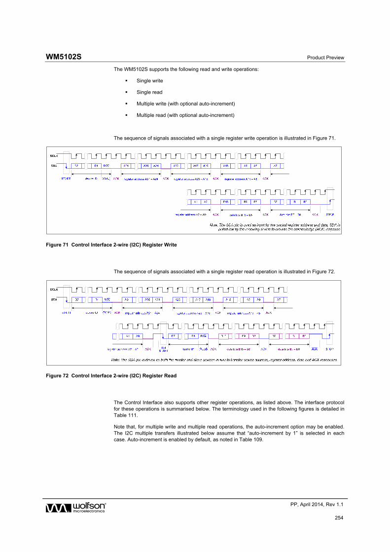
WM5102S Product Preview
w PP, April 2014, Rev 1.1
254
The WM5102S supports the following read and write operations:
Single write
Single read
Multiple write (with optional auto-increment)
Multiple read (with optional auto-increment)
The sequence of signals associated with a single register write operation is illustrated in Figure 71.
Figure 71 Control Interface 2-wire (I2C) Register Write
The sequence of signals associated with a single register read operation is illustrated in Figure 72.
Figure 72 Control Interface 2-wire (I2C) Register Read
The Control Interface also supports other register operations, as listed above. The interface protocol for these operations is summarised below. The terminology used in the following figures is detailed in Table 111.
Note that, for multiple write and multiple read operations, the auto-increment option may be enabled. The I2C multiple transfers illustrated below assume that “auto-increment by 1” is selected in each case. Auto-increment is enabled by default, as noted in Table 109.
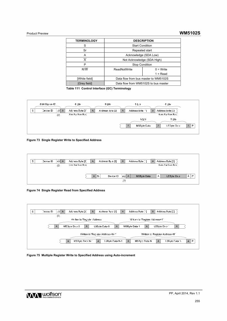
Product Preview WM5102S
w PP, April 2014, Rev 1.1
255
TERMINOLOGY DESCRIPTION
S Start Condition
Sr Repeated start
A Acknowledge (SDA Low)
A Not Acknowledge (SDA High)
P Stop Condition
R/W ReadNotWrite
0 = Write
1 = Read
[White field] Data flow from bus master to WM5102S
[Grey field] Data flow from WM5102S to bus master
Table 111 Control Interface (I2C) Terminology
Figure 73 Single Register Write to Specified Address
Figure 74 Single Register Read from Specified Address
Figure 75 Multiple Register Write to Specified Address using Auto-increment
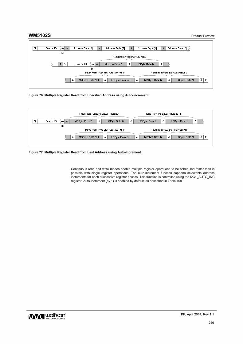
WM5102S Product Preview
w PP, April 2014, Rev 1.1
256
Figure 76 Multiple Register Read from Specified Address using Auto-increment
Figure 77 Multiple Register Read from Last Address using Auto-increment
Continuous read and write modes enable multiple register operations to be scheduled faster than is possible with single register operations. The auto-increment function supports selectable address increments for each successive register access. This function is controlled using the I2C1_AUTO_INC register. Auto-increment (by 1) is enabled by default, as described in Table 109.
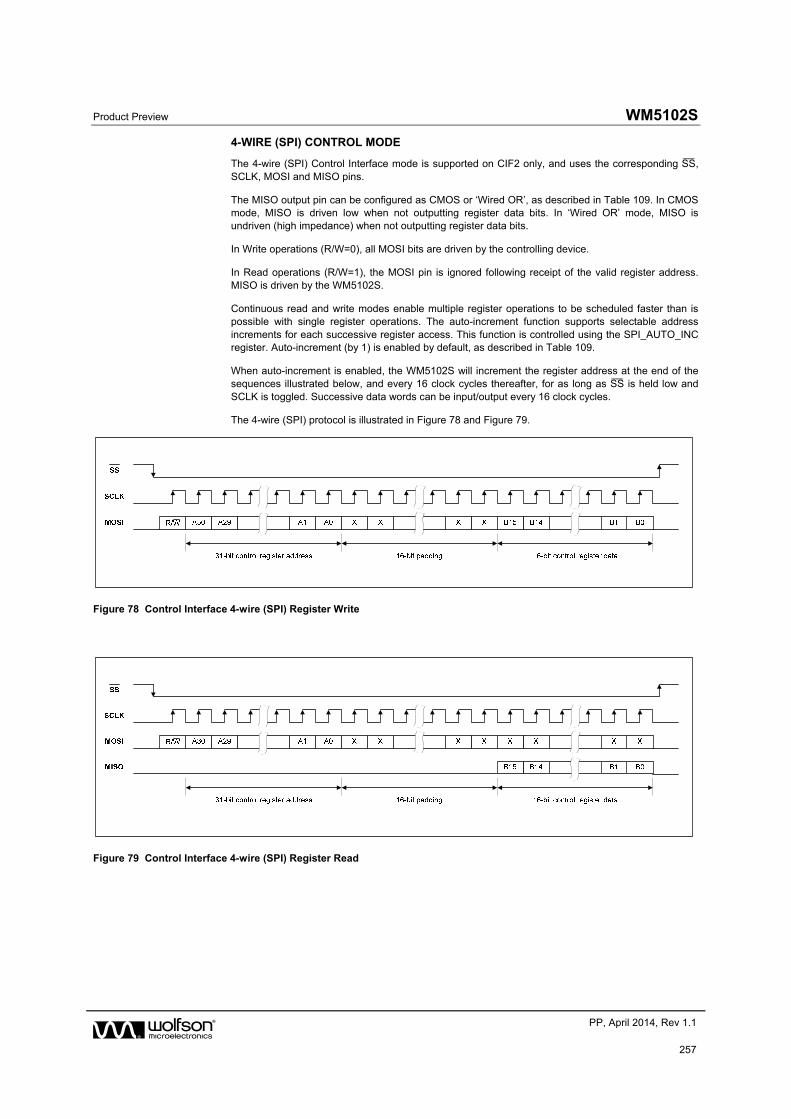
Product Preview WM5102S
w PP, April 2014, Rev 1.1
257
4-WIRE (SPI) CONTROL MODE
The 4-wire (SPI) Control Interface mode is supported on CIF2 only, and uses the corresponding SS¯¯, SCLK, MOSI and MISO pins.
The MISO output pin can be configured as CMOS or ‘Wired OR’, as described in Table 109. In CMOS mode, MISO is driven low when not outputting register data bits. In ‘Wired OR’ mode, MISO is undriven (high impedance) when not outputting register data bits.
In Write operations (R/W=0), all MOSI bits are driven by the controlling device.
In Read operations (R/W=1), the MOSI pin is ignored following receipt of the valid register address. MISO is driven by the WM5102S.
Continuous read and write modes enable multiple register operations to be scheduled faster than is possible with single register operations. The auto-increment function supports selectable address increments for each successive register access. This function is controlled using the SPI_AUTO_INC register. Auto-increment (by 1) is enabled by default, as described in Table 109.
When auto-increment is enabled, the WM5102S will increment the register address at the end of the sequences illustrated below, and every 16 clock cycles thereafter, for as long as SS¯¯ is held low and SCLK is toggled. Successive data words can be input/output every 16 clock cycles.
The 4-wire (SPI) protocol is illustrated in Figure 78 and Figure 79.
Figure 78 Control Interface 4-wire (SPI) Register Write
Figure 79 Control Interface 4-wire (SPI) Register Read
WM5102S Product Preview
w PP, April 2014, Rev 1.1
258
CONTROL WRITE SEQUENCER
The Control Write Sequencer is a programmable unit that forms part of the WM5102S control interface logic. It provides the ability to perform a sequence of register write operations with the minimum of demands on the host processor - the sequence may be initiated by a single operation from the host processor and then left to execute independently.
Default sequences for pop-suppressed start-up and shut-down of each headphone/earpiece output driver are provided (these are scheduled automatically when the respective output paths are enabled or disabled). Other control sequences can be programmed, and may be associated with Jack Detect, Wake-Up or Sample Rate Detection functions - these sequences are automatically scheduled whenever a corresponding event is detected.
When a sequence is initiated, the sequencer performs a series of pre-defined register writes. The ‘start index’ of a control sequence within the sequencer’s memory may be commanded directly by the host processor. In the case of a headphone or earpiece enable/disable event, or sequences associated with Jack Detect, Sleep Control or Sample Rate Detection, the applicable ‘start index’ is held in a user-programmed control register for each sequence.
The Control Write Sequencer may be triggered in a number of ways, as described above. Multiple sequences will be queued if necessary, and each is scheduled in turn. When all of the queued sequences have completed, the sequencer stops, and an Interrupt status flag is asserted.
A valid clock (SYSCLK) must be enabled whenever a Control Write Sequence is scheduled. See “Clocking and Sample Rates” for further details.
INITIATING A SEQUENCE
The Register fields associated with running the Control Write Sequencer are described in Table 112.
The Write Sequencer is enabled using the WSEQ_ENA bit. The index location of the first command in the selected sequence is held in the WSEQ_START_INDEX register.
Writing a ‘1’ to the WSEQ_START bit commands the sequencer to execute a control sequence, starting at the given index. Note that, if the sequencer is already running, then the WSEQ_START command will be queued, and will be executed later when the sequencer becomes available.
The Write Sequencer can be interrupted by writing a ‘1’ to the WSEQ_ABORT bit. Note that this command will only abort a sequence that is currently running; if other sequence commands are pending and not yet started, these sequences will not be aborted by writing to the WSEQ_ABORT bit.
The Write Sequencer stores up to 256 register write commands. These are defined in Registers R12288 (3000h) to R12799 (31FFh). Each of the 256 possible commands is defined in 2 control registers - see Table 117 for a description of these registers.
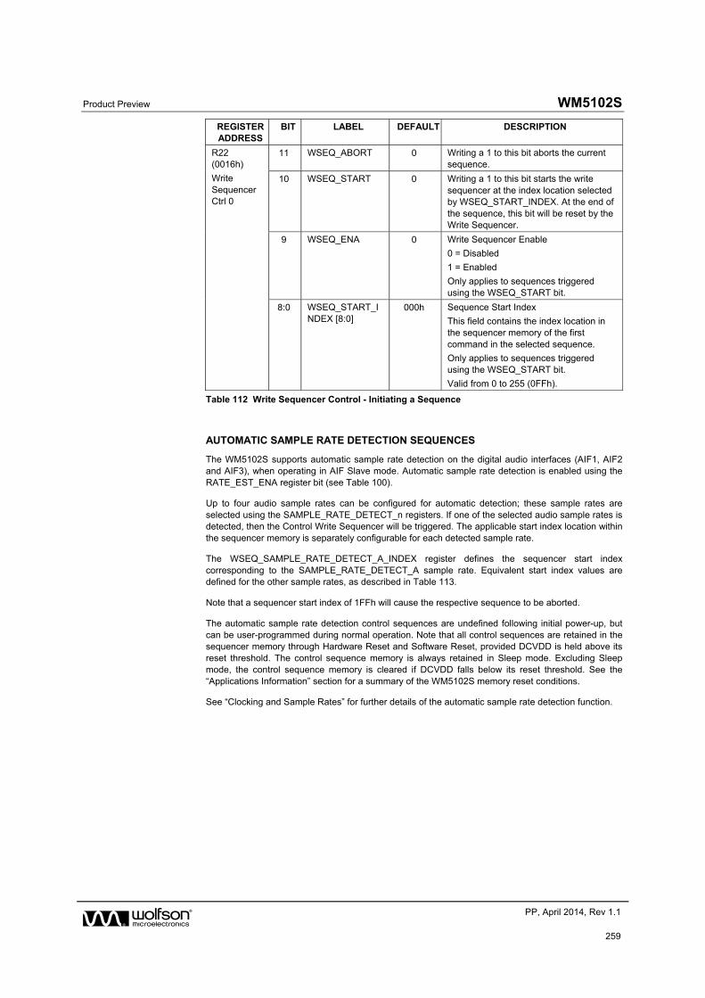
Product Preview WM5102S
w PP, April 2014, Rev 1.1
259
REGISTER ADDRESS
BIT LABEL DEFAULT DESCRIPTION
R22 (0016h)
Write Sequencer Ctrl 0
11 WSEQ_ABORT 0 Writing a 1 to this bit aborts the current sequence.
10 WSEQ_START 0 Writing a 1 to this bit starts the write sequencer at the index location selected by WSEQ_START_INDEX. At the end of the sequence, this bit will be reset by the Write Sequencer.
9 WSEQ_ENA 0 Write Sequencer Enable
0 = Disabled
1 = Enabled
Only applies to sequences triggered using the WSEQ_START bit.
8:0 WSEQ_START_INDEX [8:0]
000h Sequence Start Index
This field contains the index location in the sequencer memory of the first command in the selected sequence.
Only applies to sequences triggered using the WSEQ_START bit.
Valid from 0 to 255 (0FFh).
Table 112 Write Sequencer Control - Initiating a Sequence
AUTOMATIC SAMPLE RATE DETECTION SEQUENCES
The WM5102S supports automatic sample rate detection on the digital audio interfaces (AIF1, AIF2 and AIF3), when operating in AIF Slave mode. Automatic sample rate detection is enabled using the RATE_EST_ENA register bit (see Table 100).
Up to four audio sample rates can be configured for automatic detection; these sample rates are selected using the SAMPLE_RATE_DETECT_n registers. If one of the selected audio sample rates is detected, then the Control Write Sequencer will be triggered. The applicable start index location within the sequencer memory is separately configurable for each detected sample rate.
The WSEQ_SAMPLE_RATE_DETECT_A_INDEX register defines the sequencer start index corresponding to the SAMPLE_RATE_DETECT_A sample rate. Equivalent start index values are defined for the other sample rates, as described in Table 113.
Note that a sequencer start index of 1FFh will cause the respective sequence to be aborted.
The automatic sample rate detection control sequences are undefined following initial power-up, but can be user-programmed during normal operation. Note that all control sequences are retained in the sequencer memory through Hardware Reset and Software Reset, provided DCVDD is held above its reset threshold. The control sequence memory is always retained in Sleep mode. Excluding Sleep mode, the control sequence memory is cleared if DCVDD falls below its reset threshold. See the “Applications Information” section for a summary of the WM5102S memory reset conditions.
See “Clocking and Sample Rates” for further details of the automatic sample rate detection function.
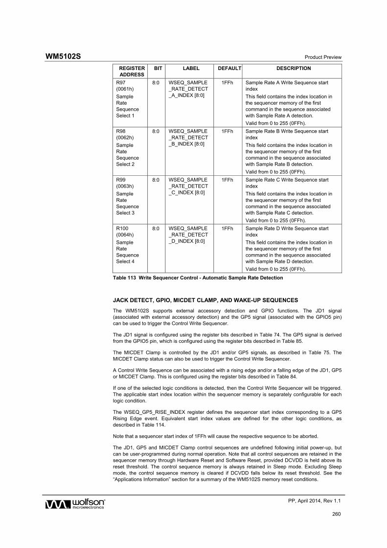
WM5102S Product Preview
w PP, April 2014, Rev 1.1
260
REGISTER ADDRESS
BIT LABEL DEFAULT DESCRIPTION
R97 (0061h)
Sample Rate Sequence Select 1
8:0 WSEQ_SAMPLE_RATE_DETECT_A_INDEX [8:0]
1FFh Sample Rate A Write Sequence start index
This field contains the index location in the sequencer memory of the first command in the sequence associated with Sample Rate A detection.
Valid from 0 to 255 (0FFh).
R98 (0062h)
Sample Rate Sequence Select 2
8:0 WSEQ_SAMPLE_RATE_DETECT_B_INDEX [8:0]
1FFh Sample Rate B Write Sequence start index
This field contains the index location in the sequencer memory of the first command in the sequence associated with Sample Rate B detection.
Valid from 0 to 255 (0FFh).
R99 (0063h)
Sample Rate Sequence Select 3
8:0 WSEQ_SAMPLE_RATE_DETECT_C_INDEX [8:0]
1FFh Sample Rate C Write Sequence start index
This field contains the index location in the sequencer memory of the first command in the sequence associated with Sample Rate C detection.
Valid from 0 to 255 (0FFh).
R100 (0064h)
Sample Rate Sequence Select 4
8:0 WSEQ_SAMPLE_RATE_DETECT_D_INDEX [8:0]
1FFh Sample Rate D Write Sequence start index
This field contains the index location in the sequencer memory of the first command in the sequence associated with Sample Rate D detection.
Valid from 0 to 255 (0FFh).
Table 113 Write Sequencer Control - Automatic Sample Rate Detection
JACK DETECT, GPIO, MICDET CLAMP, AND WAKE-UP SEQUENCES
The WM5102S supports external accessory detection and GPIO functions. The JD1 signal (associated with external accessory detection) and the GP5 signal (associated with the GPIO5 pin) can be used to trigger the Control Write Sequencer.
The JD1 signal is configured using the register bits described in Table 74. The GP5 signal is derived from the GPIO5 pin, which is configured using the register bits described in Table 85.
The MICDET Clamp is controlled by the JD1 and/or GP5 signals, as described in Table 75. The MICDET Clamp status can also be used to trigger the Control Write Sequencer.
A Control Write Sequence can be associated with a rising edge and/or a falling edge of the JD1, GP5 or MICDET Clamp. This is configured using the register bits described in Table 84.
If one of the selected logic conditions is detected, then the Control Write Sequencer will be triggered. The applicable start index location within the sequencer memory is separately configurable for each logic condition.
The WSEQ_GP5_RISE_INDEX register defines the sequencer start index corresponding to a GP5 Rising Edge event. Equivalent start index values are defined for the other logic conditions, as described in Table 114.
Note that a sequencer start index of 1FFh will cause the respective sequence to be aborted.
The JD1, GP5 and MICDET Clamp control sequences are undefined following initial power-up, but can be user-programmed during normal operation. Note that all control sequences are retained in the sequencer memory through Hardware Reset and Software Reset, provided DCVDD is held above its reset threshold. The control sequence memory is always retained in Sleep mode. Excluding Sleep mode, the control sequence memory is cleared if DCVDD falls below its reset threshold. See the “Applications Information” section for a summary of the WM5102S memory reset conditions.
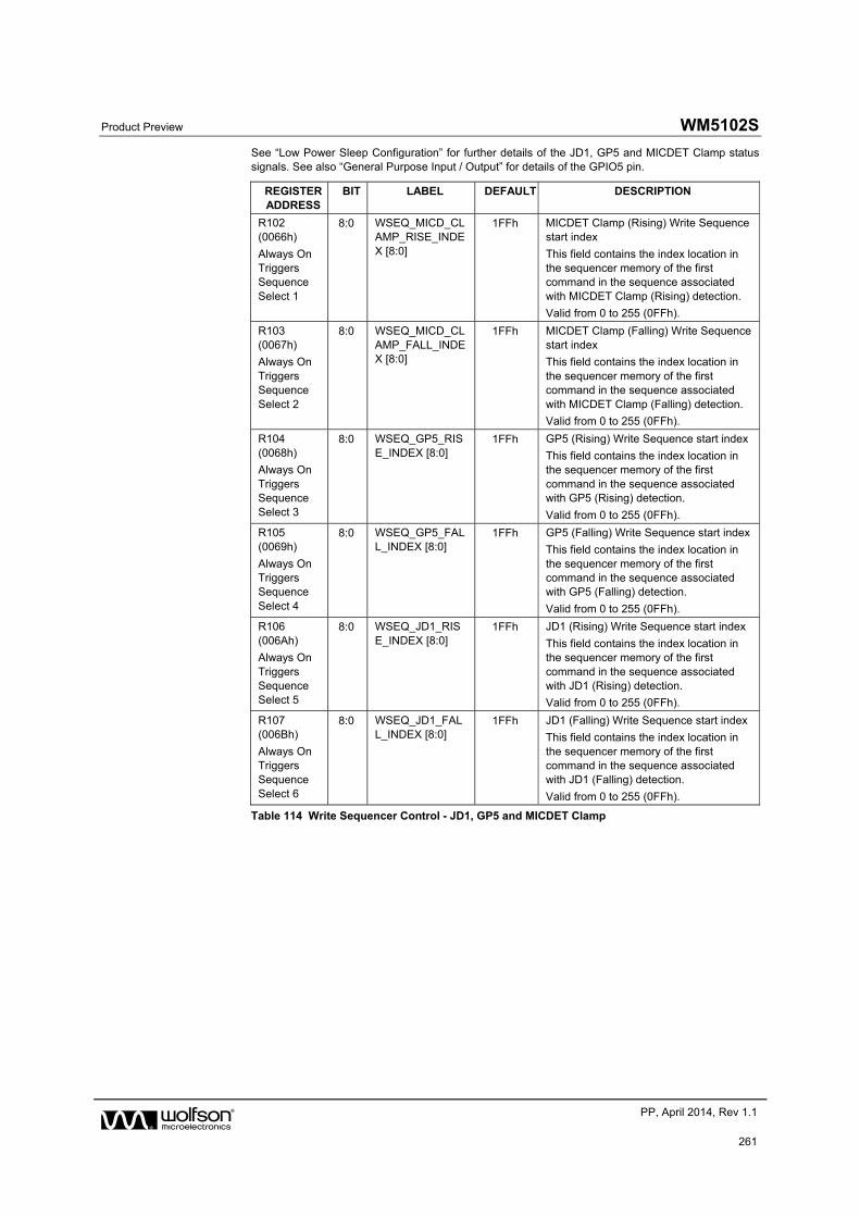
Product Preview WM5102S
w PP, April 2014, Rev 1.1
261
See “Low Power Sleep Configuration” for further details of the JD1, GP5 and MICDET Clamp status signals. See also “General Purpose Input / Output” for details of the GPIO5 pin.
REGISTER ADDRESS
BIT LABEL DEFAULT DESCRIPTION
R102 (0066h)
Always On Triggers Sequence Select 1
8:0 WSEQ_MICD_CLAMP_RISE_INDEX [8:0]
1FFh MICDET Clamp (Rising) Write Sequence start index
This field contains the index location in the sequencer memory of the first command in the sequence associated with MICDET Clamp (Rising) detection.
Valid from 0 to 255 (0FFh).
R103 (0067h)
Always On Triggers Sequence Select 2
8:0 WSEQ_MICD_CLAMP_FALL_INDEX [8:0]
1FFh MICDET Clamp (Falling) Write Sequence start index
This field contains the index location in the sequencer memory of the first command in the sequence associated with MICDET Clamp (Falling) detection.
Valid from 0 to 255 (0FFh).
R104 (0068h)
Always On Triggers Sequence Select 3
8:0 WSEQ_GP5_RISE_INDEX [8:0]
1FFh GP5 (Rising) Write Sequence start index
This field contains the index location in the sequencer memory of the first command in the sequence associated with GP5 (Rising) detection.
Valid from 0 to 255 (0FFh).
R105 (0069h)
Always On Triggers Sequence Select 4
8:0 WSEQ_GP5_FALL_INDEX [8:0]
1FFh GP5 (Falling) Write Sequence start index
This field contains the index location in the sequencer memory of the first command in the sequence associated with GP5 (Falling) detection.
Valid from 0 to 255 (0FFh).
R106 (006Ah)
Always On Triggers Sequence Select 5
8:0 WSEQ_JD1_RISE_INDEX [8:0]
1FFh JD1 (Rising) Write Sequence start index
This field contains the index location in the sequencer memory of the first command in the sequence associated with JD1 (Rising) detection.
Valid from 0 to 255 (0FFh).
R107 (006Bh)
Always On Triggers Sequence Select 6
8:0 WSEQ_JD1_FALL_INDEX [8:0]
1FFh JD1 (Falling) Write Sequence start index
This field contains the index location in the sequencer memory of the first command in the sequence associated with JD1 (Falling) detection.
Valid from 0 to 255 (0FFh).
Table 114 Write Sequencer Control - JD1, GP5 and MICDET Clamp
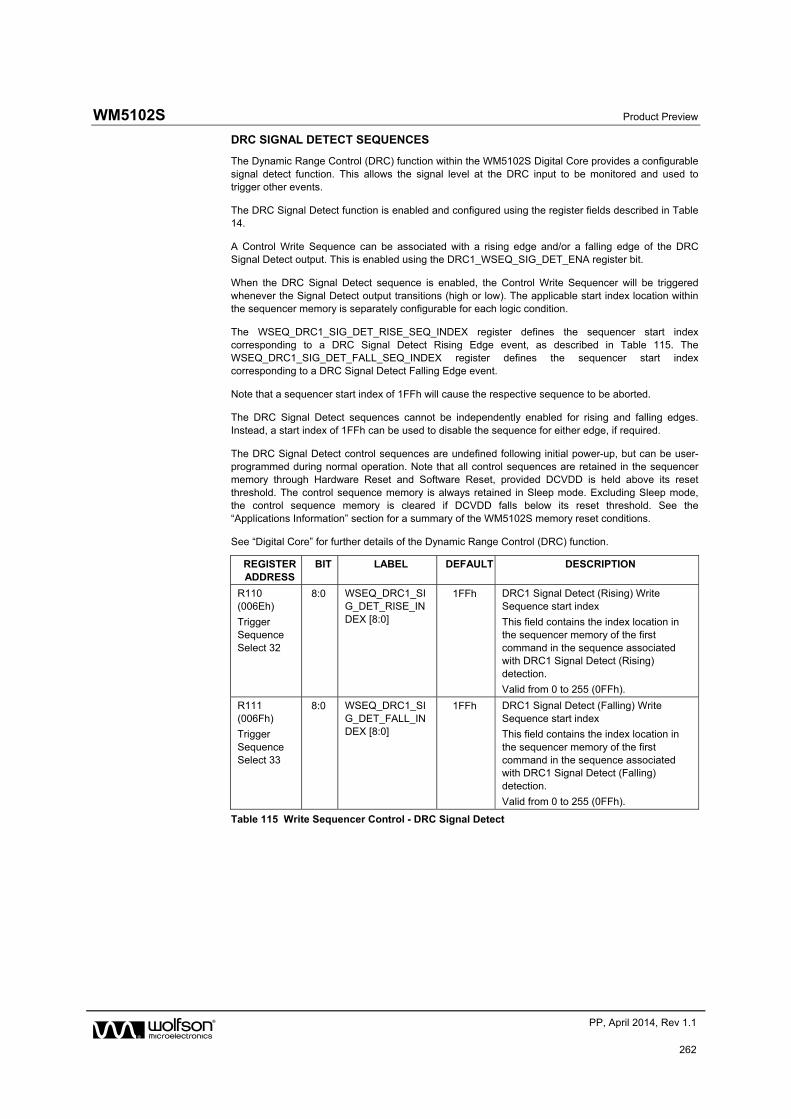
WM5102S Product Preview
w PP, April 2014, Rev 1.1
262
DRC SIGNAL DETECT SEQUENCES
The Dynamic Range Control (DRC) function within the WM5102S Digital Core provides a configurable signal detect function. This allows the signal level at the DRC input to be monitored and used to trigger other events.
The DRC Signal Detect function is enabled and configured using the register fields described in Table 14.
A Control Write Sequence can be associated with a rising edge and/or a falling edge of the DRC Signal Detect output. This is enabled using the DRC1_WSEQ_SIG_DET_ENA register bit.
When the DRC Signal Detect sequence is enabled, the Control Write Sequencer will be triggered whenever the Signal Detect output transitions (high or low). The applicable start index location within the sequencer memory is separately configurable for each logic condition.
The WSEQ_DRC1_SIG_DET_RISE_SEQ_INDEX register defines the sequencer start index corresponding to a DRC Signal Detect Rising Edge event, as described in Table 115. The WSEQ_DRC1_SIG_DET_FALL_SEQ_INDEX register defines the sequencer start index corresponding to a DRC Signal Detect Falling Edge event.
Note that a sequencer start index of 1FFh will cause the respective sequence to be aborted.
The DRC Signal Detect sequences cannot be independently enabled for rising and falling edges. Instead, a start index of 1FFh can be used to disable the sequence for either edge, if required.
The DRC Signal Detect control sequences are undefined following initial power-up, but can be user-programmed during normal operation. Note that all control sequences are retained in the sequencer memory through Hardware Reset and Software Reset, provided DCVDD is held above its reset threshold. The control sequence memory is always retained in Sleep mode. Excluding Sleep mode, the control sequence memory is cleared if DCVDD falls below its reset threshold. See the “Applications Information” section for a summary of the WM5102S memory reset conditions.
See “Digital Core” for further details of the Dynamic Range Control (DRC) function.
REGISTER ADDRESS
BIT LABEL DEFAULT DESCRIPTION
R110 (006Eh)
Trigger Sequence Select 32
8:0 WSEQ_DRC1_SIG_DET_RISE_INDEX [8:0]
1FFh DRC1 Signal Detect (Rising) Write Sequence start index
This field contains the index location in the sequencer memory of the first command in the sequence associated with DRC1 Signal Detect (Rising) detection.
Valid from 0 to 255 (0FFh).
R111 (006Fh)
Trigger Sequence Select 33
8:0 WSEQ_DRC1_SIG_DET_FALL_INDEX [8:0]
1FFh DRC1 Signal Detect (Falling) Write Sequence start index
This field contains the index location in the sequencer memory of the first command in the sequence associated with DRC1 Signal Detect (Falling) detection.
Valid from 0 to 255 (0FFh).
Table 115 Write Sequencer Control - DRC Signal Detect
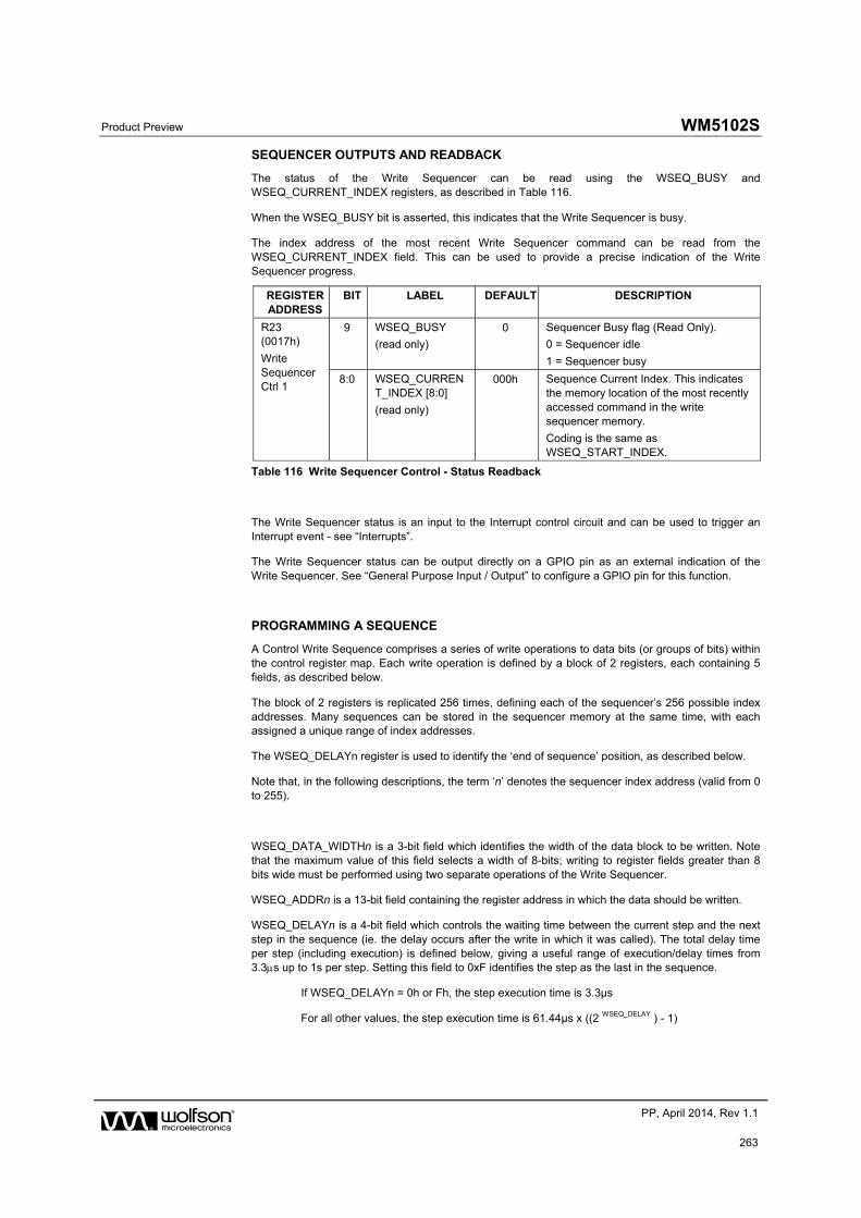
Product Preview WM5102S
w PP, April 2014, Rev 1.1
263
SEQUENCER OUTPUTS AND READBACK
The status of the Write Sequencer can be read using the WSEQ_BUSY and WSEQ_CURRENT_INDEX registers, as described in Table 116.
When the WSEQ_BUSY bit is asserted, this indicates that the Write Sequencer is busy.
The index address of the most recent Write Sequencer command can be read from the WSEQ_CURRENT_INDEX field. This can be used to provide a precise indication of the Write Sequencer progress.
REGISTER ADDRESS
BIT LABEL DEFAULT DESCRIPTION
R23 (0017h)
Write Sequencer Ctrl 1
9 WSEQ_BUSY
(read only)
0 Sequencer Busy flag (Read Only).
0 = Sequencer idle
1 = Sequencer busy
8:0 WSEQ_CURRENT_INDEX [8:0]
(read only)
000h Sequence Current Index. This indicates the memory location of the most recently accessed command in the write sequencer memory.
Coding is the same as WSEQ_START_INDEX.
Table 116 Write Sequencer Control - Status Readback
The Write Sequencer status is an input to the Interrupt control circuit and can be used to trigger an Interrupt event - see “Interrupts”.
The Write Sequencer status can be output directly on a GPIO pin as an external indication of the Write Sequencer. See “General Purpose Input / Output” to configure a GPIO pin for this function.
PROGRAMMING A SEQUENCE
A Control Write Sequence comprises a series of write operations to data bits (or groups of bits) within the control register map. Each write operation is defined by a block of 2 registers, each containing 5 fields, as described below.
The block of 2 registers is replicated 256 times, defining each of the sequencer’s 256 possible index addresses. Many sequences can be stored in the sequencer memory at the same time, with each assigned a unique range of index addresses.
The WSEQ_DELAYn register is used to identify the ‘end of sequence’ position, as described below.
Note that, in the following descriptions, the term ‘n’ denotes the sequencer index address (valid from 0 to 255).
WSEQ_DATA_WIDTHn is a 3-bit field which identifies the width of the data block to be written. Note that the maximum value of this field selects a width of 8-bits; writing to register fields greater than 8 bits wide must be performed using two separate operations of the Write Sequencer.
WSEQ_ADDRn is a 13-bit field containing the register address in which the data should be written.
WSEQ_DELAYn is a 4-bit field which controls the waiting time between the current step and the next step in the sequence (ie. the delay occurs after the write in which it was called). The total delay time per step (including execution) is defined below, giving a useful range of execution/delay times from 3.3s up to 1s per step. Setting this field to 0xF identifies the step as the last in the sequence.
If WSEQ_DELAYn = 0h or Fh, the step execution time is 3.3µs
For all other values, the step execution time is 61.44µs x ((2 WSEQ_DELAY ) - 1)
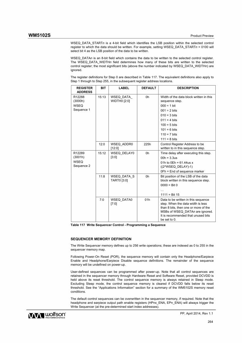
WM5102S Product Preview
w PP, April 2014, Rev 1.1
264
WSEQ_DATA_STARTn is a 4-bit field which identifies the LSB position within the selected control register to which the data should be written. For example, setting WSEQ_DATA_STARTn = 0100 will select bit 4 as the LSB position of the data to be written.
WSEQ_DATAn is an 8-bit field which contains the data to be written to the selected control register. The WSEQ_DATA_WIDTHn field determines how many of these bits are written to the selected control register; the most significant bits (above the number indicated by WSEQ_DATA_WIDTHn) are ignored.
The register definitions for Step 0 are described in Table 117. The equivalent definitions also apply to Step 1 through to Step 255, in the subsequent register address locations.
REGISTER ADDRESS
BIT LABEL DEFAULT DESCRIPTION
R12288 (3000h)
WSEQ Sequence 1
15:13 WSEQ_DATA_WIDTH0 [2:0]
0h Width of the data block written in this sequence step.
000 = 1 bit
001 = 2 bits
010 = 3 bits
011 = 4 bits
100 = 5 bits
101 = 6 bits
110 = 7 bits
111 = 8 bits
12:0 WSEQ_ADDR0 [12:0]
225h Control Register Address to be written to in this sequence step.
R12289 (3001h)
WSEQ Sequence 2
15:12 WSEQ_DELAY0 [3:0]
0h Time delay after executing this step.
00h = 3.3us
01h to 0Eh = 61.44us x ((2^WSEQ_DELAY)-1)
0Fh = End of sequence marker
11:8 WSEQ_DATA_START0 [3:0]
0h Bit position of the LSB of the data block written in this sequence step.
0000 = Bit 0
…
1111 = Bit 15
7:0 WSEQ_DATA0 [7:0]
01h Data to be written in this sequence step. When the data width is less than 8 bits, then one or more of the MSBs of WSEQ_DATAn are ignored. It is recommended that unused bits be set to 0.
Table 117 Write Sequencer Control - Programming a Sequence
SEQUENCER MEMORY DEFINITION
The Write Sequencer memory defines up to 256 write operations; these are indexed as 0 to 255 in the sequencer memory map.
Following Power-On Reset (POR), the sequence memory will contain only the Headphone/Earpiece Enable and Headphone/Earpiece Disable sequence definitions. The remainder of the sequence memory will be undefined on power-up.
User-defined sequences can be programmed after power-up. Note that all control sequences are retained in the sequencer memory through Hardware Reset and Software Reset, provided DCVDD is held above its reset threshold. The control sequence memory is always retained in Sleep mode. Excluding Sleep mode, the control sequence memory is cleared if DCVDD falls below its reset threshold. See the “Applications Information” section for a summary of the WM5102S memory reset conditions.
The default control sequences can be overwritten in the sequencer memory, if required. Note that the headphone and earpiece output path enable registers (HPnx_ENA, EPn_ENA) will always trigger the Write Sequencer (at the pre-determined start index addresses).
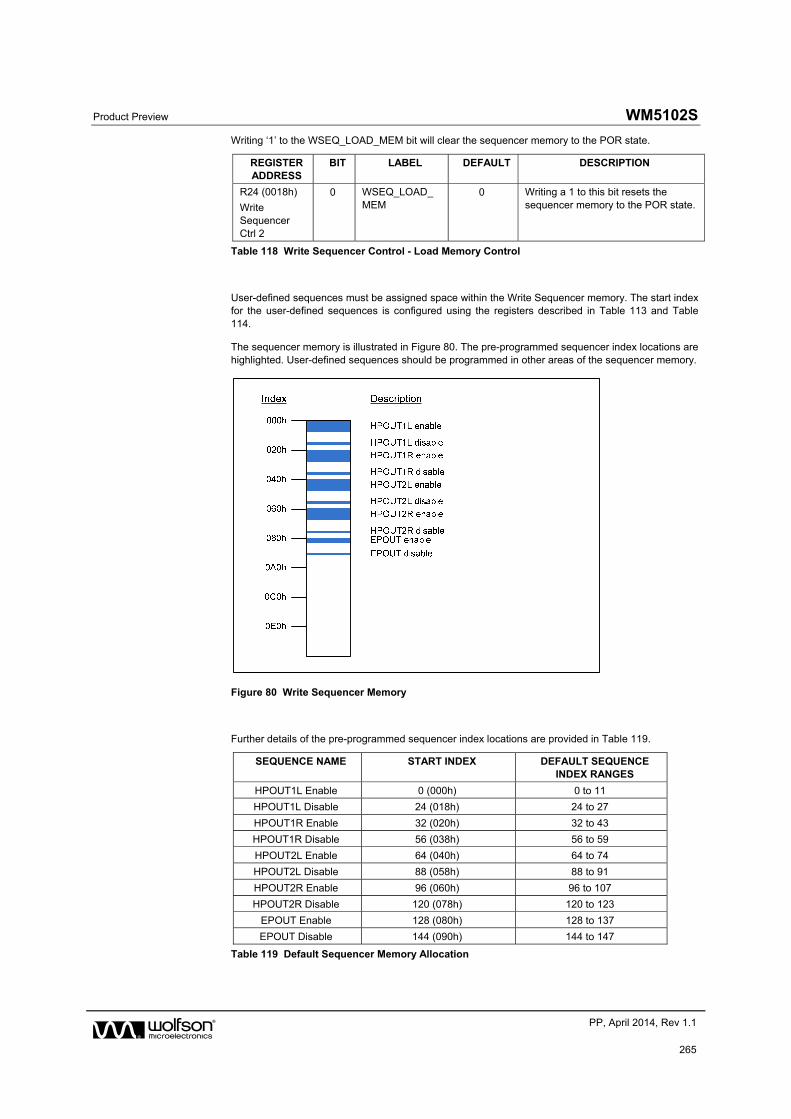
Product Preview WM5102S
w PP, April 2014, Rev 1.1
265
Writing ‘1’ to the WSEQ_LOAD_MEM bit will clear the sequencer memory to the POR state.
REGISTER ADDRESS
BIT LABEL DEFAULT DESCRIPTION
R24 (0018h)
Write Sequencer Ctrl 2
0 WSEQ_LOAD_MEM
0 Writing a 1 to this bit resets the sequencer memory to the POR state.
Table 118 Write Sequencer Control - Load Memory Control
User-defined sequences must be assigned space within the Write Sequencer memory. The start index for the user-defined sequences is configured using the registers described in Table 113 and Table 114.
The sequencer memory is illustrated in Figure 80. The pre-programmed sequencer index locations are highlighted. User-defined sequences should be programmed in other areas of the sequencer memory.
Figure 80 Write Sequencer Memory
Further details of the pre-programmed sequencer index locations are provided in Table 119.
SEQUENCE NAME START INDEX DEFAULT SEQUENCE INDEX RANGES
HPOUT1L Enable 0 (000h) 0 to 11
HPOUT1L Disable 24 (018h) 24 to 27
HPOUT1R Enable 32 (020h) 32 to 43
HPOUT1R Disable 56 (038h) 56 to 59
HPOUT2L Enable 64 (040h) 64 to 74
HPOUT2L Disable 88 (058h) 88 to 91
HPOUT2R Enable 96 (060h) 96 to 107
HPOUT2R Disable 120 (078h) 120 to 123
EPOUT Enable 128 (080h) 128 to 137
EPOUT Disable 144 (090h) 144 to 147
Table 119 Default Sequencer Memory Allocation
WM5102S Product Preview
w PP, April 2014, Rev 1.1
266
CHARGE PUMPS, REGULATORS AND VOLTAGE REFERENCE
The WM5102S incorporates two Charge Pump circuits and two LDO Regulator circuits to generate supply rails for internal functions and to support external microphone requirements. The WM5102S also provides three MICBIAS generators which provide low noise reference voltages suitable for biasing electret condenser (ECM) type microphones or powering digital microphones.
Refer to the “Applications Information” section for recommended external components.
CHARGE PUMPS AND LDO2 REGULATOR
Charge Pump 1 (CP1) is used to generate the positive and negative supply rails for the analogue output drivers. CP1 is enabled automatically by the WM5102S when required by the output drivers.
Charge Pump 2 (CP2) powers LDO2, which provides the supply rail for analogue input circuits and for the MICBIAS generators. CP2 and LDO2 are enabled using the CP2_ENA register bit.
The 32kHz clock must be configured and enabled when using CP2. See “Clocking and Sample Rates” for details of the system clocks.
When CP2 and LDO2 are enabled, the MICVDD voltage can be selected using the LDO2_VSEL control field. Note that, when one or more of the MICBIAS generators is operating in normal (regulator) mode, then the MICVDD voltage must be at least 200mV greater than the highest selected MICBIASn output voltage(s).
When CP2 and LDO2 are enabled, an internal bypass path may be selected, connecting the MICVDD pin directly to the CPVDD supply. This path is controlled using the CP2_BYPASS register. Note that the bypass path is only supported when CP2 is enabled.
When CP2 is disabled, the CP2VOUT pin can be configured to be floating or to be actively discharged. This is selected using the CP2_DISCH register bit.
When LDO2 is disabled, the MICVDD pin can be configured to be floating or to be actively discharged. This is selected using the LDO2_DISCH register bit.
The MICVDD pin is connected to the output of LDO2. Note that the MICVDD does not support direct connection to an external supply; MICVDD is always powered internally to the WM5102S.
The Charge Pumps and LDO2 Regulator circuits are illustrated in Figure 81. The associated register control bits are described in Table 120.
Note that decoupling capacitors and flyback capacitors are required for these circuits. Refer to the “Applications Information” section for recommended external components.
MICBIAS BIAS (MICBIAS) CONTROL
There are three MICBIAS generators which provide low noise reference voltages suitable for biasing electret condenser (ECM) type microphones or powering digital microphones. Refer to the “Applications Information” section for recommended external components.
The MICBIAS generators are powered from MICVDD, which is generated by an internal Charge Pump and LDO, as illustrated in Figure 81.
The MICBIAS outputs can be independently enabled using the MICBn_ENA register bits (where n = 1, 2 or 3 for MICBIAS1, 2 or 3 respectively).
When a MICBIAS output is disabled, the output pin can be configured to be floating or to be actively discharged. This is selected using the MICBn_DISCH register bits.
The MICBIAS generators can each operate as a voltage regulator or in bypass mode. The applicable mode is selected using the MICBn_BYPASS registers.
In Regulator mode, the output voltage is selected using the MICBn_LVL register bits. In this mode, MICVDD must be at least 200mV greater than the required MICBIAS output voltages. The MICBIAS

Product Preview WM5102S
w PP, April 2014, Rev 1.1
267
outputs are powered from the MICVDD pin, and use the internal bandgap circuit as a reference.
In Regulator mode, the MICBIAS regulators are designed to operate without external decoupling capacitors. The regulators can be configured to support a capacitive load if required, using the MICBn_EXT_CAP register bits. (This may be appropriate for a digital microphone supply.) It is important that the external capacitance is compatible with the applicable MICBn_EXT_CAP setting. The compatible load conditions are detailed in the “Electrical Characteristics” section.
In Bypass mode, the output pin (MICBIAS1, MICBIAS2 or MICBIAS3) is connected directly to MICVDD. This enables a low power operating state. Note that the MICBn_EXT_CAP register settings are not applicable in Bypass mode; there are no restrictions on the external MICBIAS capacitance in Bypass mode.
The MICBIAS generators incorporate a pop-free control circuit to ensure smooth transitions when the MICBIAS outputs are enabled or disabled in Bypass mode; this feature is enabled using the MICBn_RATE registers.
The MICBIAS generators are illustrated in Figure 81. The MICBIAS control register bits are described in Table 120.
The maximum output current for each MICBIASn pin is noted in the “Electrical Characteristics”. This limit must be observed on each MICBIAS output, especially if more than one microphone is connected to a single MICBIAS pin. Note that the maximum output current differs between Regulator mode and Bypass mode.
VOLTAGE REFERENCE CIRCUIT
The WM5102S incorporates a voltage reference circuit, powered by AVDD. This circuit ensures the accuracy of the LDO Regulator and MICBIAS voltage settings.
LDO1 REGULATOR AND DCVDD SUPPLY
The LDO1 voltage regulator is intended for generating the DCVDD domain, which powers the digital core functions on the WM5102S. In this configuration, the LDO output (LDOVOUT) should be connected to the DCVDD pin. Note that the use of the LDO1 regulator to power external circuits cannot be supported by the WM5102S.
LDO1 is powered by LDOVDD and can be controlled using hardware or software controls. Note that, depending on the application requirements, it may be necessary to use both the hardware and software enables for LDO1, as described below.
Under hardware control, LDO1 is enabled when a logic ‘1’ is applied to the LDOENA pin. The logic level is determined with respect to the DBVDD1 voltage domain. LDO1 is also enabled when the LDO1_ENA software control register is set to 1. Note that, to disable LDO1, the hardware and software controls must both be de-asserted.
When LDO1 is enabled, an internal bypass path may be selected, connecting the LDOVOUT pin directly to the LDOVDD supply. This path is controlled using the LDO1_BYPASS register. Note that the bypass path is only supported when LDO1 is enabled.
When LDO1 is disabled, the LDOVOUT pin can be configured to be floating or to be actively discharged. This is selected using the LDO1_DISCH register bit.
When LDO1 is enabled, the LDOVOUT voltage can be controlled using the LDO1_VSEL register. Setting LDO1_HI_PWR=1 will override the LDO1_VSEL register and select 1.8V LDO output voltage. Note that, under default conditions, LDO1_HI_PWR is set to ‘1’.
It is possible to supply DCVDD from an external supply. In this configuration, the LDOVOUT pin should be left floating; the LDOVOUT pin must not be connected to the DCVDD pin in this case.
For recommended use of the Sleep / Wake-Up functions (see “Low Power Sleep Configuration”), it is assumed that DCVDD is powered from the output of LDO1. In this case, Sleep mode is selected when LDO1 is disabled, causing the DCVDD supply to be removed. Note that the AVDD, DBVDD1, and LDOVDD supplies must be present throughout the Sleep mode duration.
WM5102S Product Preview
w PP, April 2014, Rev 1.1
268
If DCVDD is powered externally (not from LDO1), then the ISOLATE_DCVDD1 register bit must be controlled as described in Table 120 when selecting WM5102S Sleep mode. In this case, Sleep mode is selected by setting the ISOLATE_DCVDD1 register bit, and then removing the DCVDD supply. For applications where DCVDD is powered externally, only the AVDD and DBVDD1 supplies are required in Sleep mode.
An internal pull-down resistor is enabled by default on the LDOENA pin. This is configurable using the LDO1ENA_PD register bit.
If DCVDD is powered from LDO1, then a logic ‘1’ must be applied to the LDOENA pin during power-up, to enable LDO1. The LDO must also be enabled using the LDOENA pin following a Hardware Reset or Software Reset, to allow the device to re-start. (It is recommended that the LDOENA pin is asserted before any reset, and is held at logic ‘1’ until after the reset is complete; this ensures the Write Sequencer and DSP firmware memory contents are retained, and also allows faster reset time.)
For normal operation following Power-On Reset (POR), Hardware Reset, or Software Reset, LDO1 must be enabled using the hardware or software controls described above. Note that when the LDO1_ENA bit is set to 1, the LDOENA pin has no effect and may be de-asserted - the LDO is then under software control, allowing Sleep mode to be selected under register control, including via the Control Write Sequencer.
See “Power-On Reset (POR) and Hardware Reset” and “Software Reset, Wake-Up, and Device ID” for details of WM5102S Resets. See also “Low Power Sleep Configuration” for details of the Sleep / Wake-up functions.
The LDO1 Regulator circuit is illustrated in Figure 81. The associated register control bits are described in Table 120.
Note that a decoupling capacitor is recommended. Refer to the “Applications Information” section for recommended external components.
BLOCK DIAGRAM AND CONTROL REGISTERS
The Charge Pump and Regulator circuits are illustrated in Figure 81. Note that decoupling capacitors and flyback capacitors are required for these circuits. Refer to the “Applications Information” section for recommended external components.
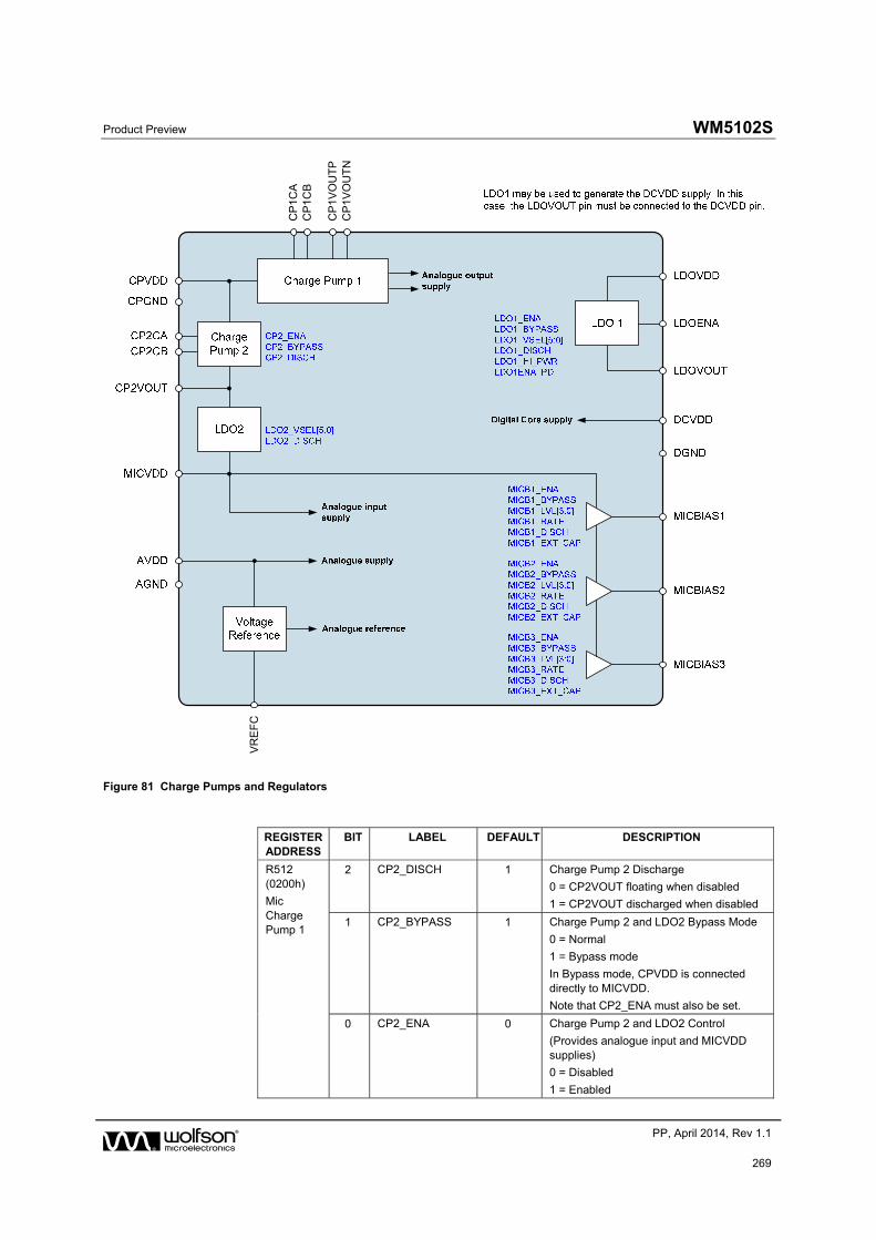
Product Preview WM5102S
w PP, April 2014, Rev 1.1
269
VR
EF
C
CP
1C
A
CP
1V
OU
TP
CP
1V
OU
TN
CP
1C
B
Figure 81 Charge Pumps and Regulators
REGISTER ADDRESS
BIT LABEL DEFAULT DESCRIPTION
R512 (0200h)
Mic Charge Pump 1
2 CP2_DISCH 1 Charge Pump 2 Discharge
0 = CP2VOUT floating when disabled
1 = CP2VOUT discharged when disabled
1 CP2_BYPASS 1 Charge Pump 2 and LDO2 Bypass Mode
0 = Normal
1 = Bypass mode
In Bypass mode, CPVDD is connected directly to MICVDD.
Note that CP2_ENA must also be set.
0 CP2_ENA 0 Charge Pump 2 and LDO2 Control
(Provides analogue input and MICVDD supplies)
0 = Disabled
1 = Enabled
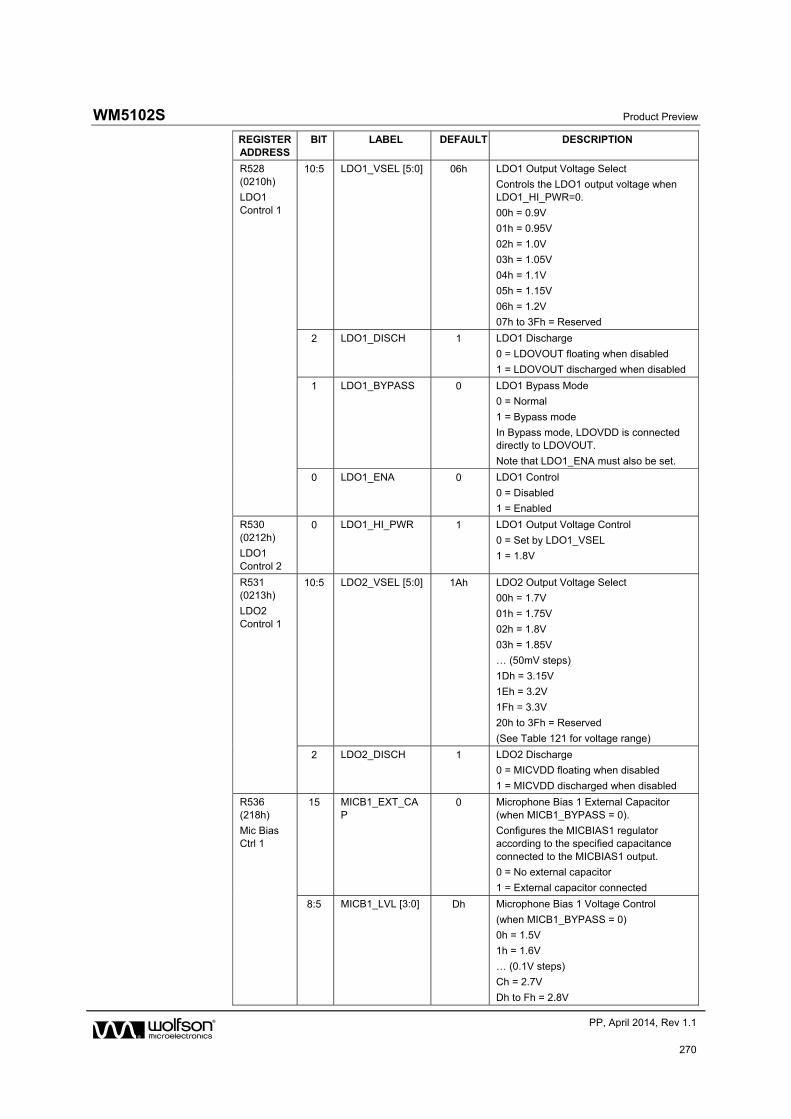
WM5102S Product Preview
w PP, April 2014, Rev 1.1
270
REGISTER ADDRESS
BIT LABEL DEFAULT DESCRIPTION
R528 (0210h)
LDO1 Control 1
10:5 LDO1_VSEL [5:0] 06h LDO1 Output Voltage Select
Controls the LDO1 output voltage when LDO1_HI_PWR=0.
00h = 0.9V
01h = 0.95V
02h = 1.0V
03h = 1.05V
04h = 1.1V
05h = 1.15V
06h = 1.2V
07h to 3Fh = Reserved
2 LDO1_DISCH 1 LDO1 Discharge
0 = LDOVOUT floating when disabled
1 = LDOVOUT discharged when disabled
1 LDO1_BYPASS 0 LDO1 Bypass Mode
0 = Normal
1 = Bypass mode
In Bypass mode, LDOVDD is connected directly to LDOVOUT.
Note that LDO1_ENA must also be set.
0 LDO1_ENA 0 LDO1 Control
0 = Disabled
1 = Enabled
R530 (0212h)
LDO1 Control 2
0 LDO1_HI_PWR 1 LDO1 Output Voltage Control
0 = Set by LDO1_VSEL
1 = 1.8V
R531 (0213h)
LDO2 Control 1
10:5 LDO2_VSEL [5:0] 1Ah LDO2 Output Voltage Select
00h = 1.7V
01h = 1.75V
02h = 1.8V
03h = 1.85V
… (50mV steps)
1Dh = 3.15V
1Eh = 3.2V
1Fh = 3.3V
20h to 3Fh = Reserved
(See Table 121 for voltage range)
2 LDO2_DISCH 1 LDO2 Discharge
0 = MICVDD floating when disabled
1 = MICVDD discharged when disabled
R536 (218h)
Mic Bias Ctrl 1
15 MICB1_EXT_CAP
0 Microphone Bias 1 External Capacitor (when MICB1_BYPASS = 0).
Configures the MICBIAS1 regulator according to the specified capacitance connected to the MICBIAS1 output.
0 = No external capacitor
1 = External capacitor connected
8:5 MICB1_LVL [3:0] Dh Microphone Bias 1 Voltage Control
(when MICB1_BYPASS = 0)
0h = 1.5V
1h = 1.6V
… (0.1V steps)
Ch = 2.7V
Dh to Fh = 2.8V
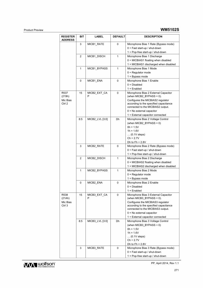
Product Preview WM5102S
w PP, April 2014, Rev 1.1
271
REGISTER ADDRESS
BIT LABEL DEFAULT DESCRIPTION
3 MICB1_RATE 0 Microphone Bias 1 Rate (Bypass mode)
0 = Fast start-up / shut-down
1 = Pop-free start-up / shut-down
2 MICB1_DISCH 1 Microphone Bias 1 Discharge
0 = MICBIAS1 floating when disabled
1 = MICBIAS1 discharged when disabled
1 MICB1_BYPASS 1 Microphone Bias 1 Mode
0 = Regulator mode
1 = Bypass mode
0 MICB1_ENA 0 Microphone Bias 1 Enable
0 = Disabled
1 = Enabled
R537 (219h)
Mic Bias Ctrl 2
15 MICB2_EXT_CAP
0 Microphone Bias 2 External Capacitor (when MICB2_BYPASS = 0).
Configures the MICBIAS2 regulator according to the specified capacitance connected to the MICBIAS2 output.
0 = No external capacitor
1 = External capacitor connected
8:5 MICB2_LVL [3:0] Dh Microphone Bias 2 Voltage Control
(when MICB2_BYPASS = 0)
0h = 1.5V 1h = 1.6V … (0.1V steps) Ch = 2.7V
Dh to Fh = 2.8V
3 MICB2_RATE 0 Microphone Bias 2 Rate (Bypass mode)
0 = Fast start-up / shut-down
1 = Pop-free start-up / shut-down
2 MICB2_DISCH 1 Microphone Bias 2 Discharge
0 = MICBIAS2 floating when disabled
1 = MICBIAS2 discharged when disabled
1 MICB2_BYPASS 1 Microphone Bias 2 Mode
0 = Regulator mode
1 = Bypass mode
0 MICB2_ENA 0 Microphone Bias 2 Enable
0 = Disabled
1 = Enabled
R538 (21Ah)
Mic Bias Ctrl 3
15 MICB3_EXT_CAP
0 Microphone Bias 3 External Capacitor (when MICB3_BYPASS = 0).
Configures the MICBIAS3 regulator according to the specified capacitance connected to the MICBIAS3 output.
0 = No external capacitor
1 = External capacitor connected
8:5 MICB3_LVL [3:0] Dh Microphone Bias 3 Voltage Control
(when MICB3_BYPASS = 0)
0h = 1.5V 1h = 1.6V … (0.1V steps) Ch = 2.7V
Dh to Fh = 2.8V
3 MICB3_RATE 0 Microphone Bias 3 Rate (Bypass mode)
0 = Fast start-up / shut-down
1 = Pop-free start-up / shut-down
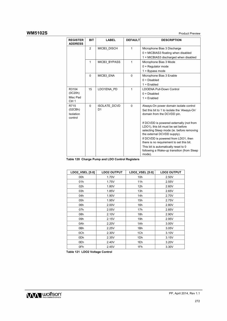
WM5102S Product Preview
w PP, April 2014, Rev 1.1
272
REGISTER ADDRESS
BIT LABEL DEFAULT DESCRIPTION
2 MICB3_DISCH 1 Microphone Bias 3 Discharge
0 = MICBIAS3 floating when disabled
1 = MICBIAS3 discharged when disabled
1 MICB3_BYPASS 1 Microphone Bias 3 Mode
0 = Regulator mode
1 = Bypass mode
0 MICB3_ENA 0 Microphone Bias 3 Enable
0 = Disabled
1 = Enabled
R3104 (0C20h)
Misc Pad Ctrl 1
15 LDO1ENA_PD 1 LDOENA Pull-Down Control
0 = Disabled
1 = Enabled
R715 (02CBh)
Isolation control
0 ISOLATE_DCVDD1
0 Always-On power domain isolate control
Set this bit to 1 to isolate the ‘Always-On’ domain from the DCVDD pin.
If DCVDD is powered externally (not from LDO1), this bit must be set before selecting Sleep mode (ie. before removing the external DCVDD supply).
If DCVDD is powered from LDO1, then there is no requirement to set this bit.
This bit is automatically reset to 0 following a Wake-up transition (from Sleep mode).
Table 120 Charge Pump and LDO Control Registers
LDO2_VSEL [5:0] LDO2 OUTPUT LDO2_VSEL [5:0] LDO2 OUTPUT
00h 1.70V 10h 2.50V
01h 1.75V 11h 2.55V
02h 1.80V 12h 2.60V
03h 1.85V 13h 2.65V
04h 1.90V 14h 2.70V
05h 1.95V 15h 2.75V
06h 2.00V 16h 2.80V
07h 2.05V 17h 2.85V
08h 2.10V 18h 2.90V
09h 2.15V 19h 2.95V
0Ah 2.20V 1Ah 3.00V
0Bh 2.25V 1Bh 3.05V
0Ch 2.30V 1Ch 3.10V
0Dh 2.35V 1Dh 3.15V
0Eh 2.40V 1Eh 3.20V
0Fh 2.45V 1Fh 3.30V
Table 121 LDO2 Voltage Control
Product Preview WM5102S
w PP, April 2014, Rev 1.1
273
JTAG INTERFACE
The JTAG interface provides test and debug access to the WM5102S DSP core. The interface comprises 5 pins, as detailed below.
TCK: Clock input
TDI: Data input
TDO: Data output
TMS: Mode select input
TRST: Test Access Port reset input (active low, internal pull-down)
For normal operation (test and debug access disabled), the JTAG interface should be held in reset (ie. TRST should be at logic 0). An internal pull-down resistor holds the TRST pin low when not actively driven.
The other JTAG input pins (TCK, TDI, TMSDSP) should also be held at logic 0 for normal operation.
THERMAL SHUTDOWN
The WM5102S incorporates a temperature sensor which detects when the device temperature is within normal limits or if the device is approaching a hazardous temperature condition.
The temperature sensor is an input to the Interrupt control circuit and can be used to trigger an Interrupt event - see “Interrupts”.
The Warning Temperature and Shutdown Temperature status flags can be output directly on a GPIO pin as an external indication of the temperature sensor. See “General Purpose Input / Output” to configure a GPIO pin for this function.
It is strongly recommended that the speaker drivers be disabled if the Shutdown Temperature condition occurs.
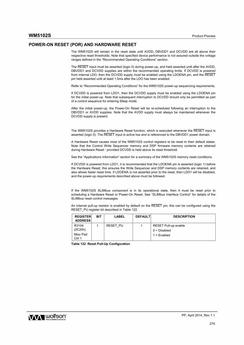
WM5102S Product Preview
w PP, April 2014, Rev 1.1
274
POWER-ON RESET (POR) AND HARDWARE RESET
The WM5102S will remain in the reset state until AVDD, DBVDD1 and DCVDD are all above their respective reset thresholds. Note that specified device performance is not assured outside the voltage ranges defined in the “Recommended Operating Conditions” section.
The RESET¯¯¯¯¯¯ input must be asserted (logic 0) during power-up, and held asserted until after the AVDD, DBVDD1 and DCVDD supplies are within the recommended operating limits. If DCVDD is powered from internal LDO, then the DCVDD supply must be enabled using the LDOENA pin, and the RESET¯¯¯¯¯¯ pin held asserted until at least 1.5ms after the LDO has been enabled.
Refer to “Recommended Operating Conditions” for the WM5102S power-up sequencing requirements.
If DCVDD is powered from LDO1, then the DCVDD supply must be enabled using the LDOENA pin for the initial power-up. Note that subsequent interruption to DCVDD should only be permitted as part of a control sequence for entering Sleep mode.
After the initial power-up, the Power-On Reset will be re-scheduled following an interruption to the DBVDD1 or AVDD supplies. Note that the AVDD supply must always be maintained whenever the DCVDD supply is present.
The WM5102S provides a Hardware Reset function, which is executed whenever the RESET¯¯¯¯¯¯ input is asserted (logic 0). The RESET¯¯¯¯¯¯ input is active low and is referenced to the DBVDD1 power domain.
A Hardware Reset causes most of the WM5102S control registers to be reset to their default states. Note that the Control Write Sequencer memory and DSP firmware memory contents are retained during Hardware Reset - provided DCVDD is held above its reset threshold.
See the “Applications Information” section for a summary of the WM5102S memory reset conditions.
If DCVDD is powered from LDO1, it is recommended that the LDOENA pin is asserted (logic 1) before the Hardware Reset; this ensures the Write Sequencer and DSP memory contents are retained, and also allows faster reset time. If LDOENA is not asserted prior to the reset, then LDO1 will be disabled, and the power-up requirements described above must be followed.
If the WM5102S SLIMbus component is in its operational state, then it must be reset prior to scheduling a Hardware Reset or Power-On Reset. See “SLIMbus Interface Control” for details of the SLIMbus reset control messages.
An internal pull-up resistor is enabled by default on the RESET¯¯¯¯¯¯ pin; this can be configured using the RESET_PU register bit described in Table 122.
REGISTER ADDRESS
BIT LABEL DEFAULT DESCRIPTION
R3104 (0C20h)
Misc Pad Ctrl 1
1 RESET_PU 1 RESET Pull-up enable
0 = Disabled
1 = Enabled
Table 122 Reset Pull-Up Configuration
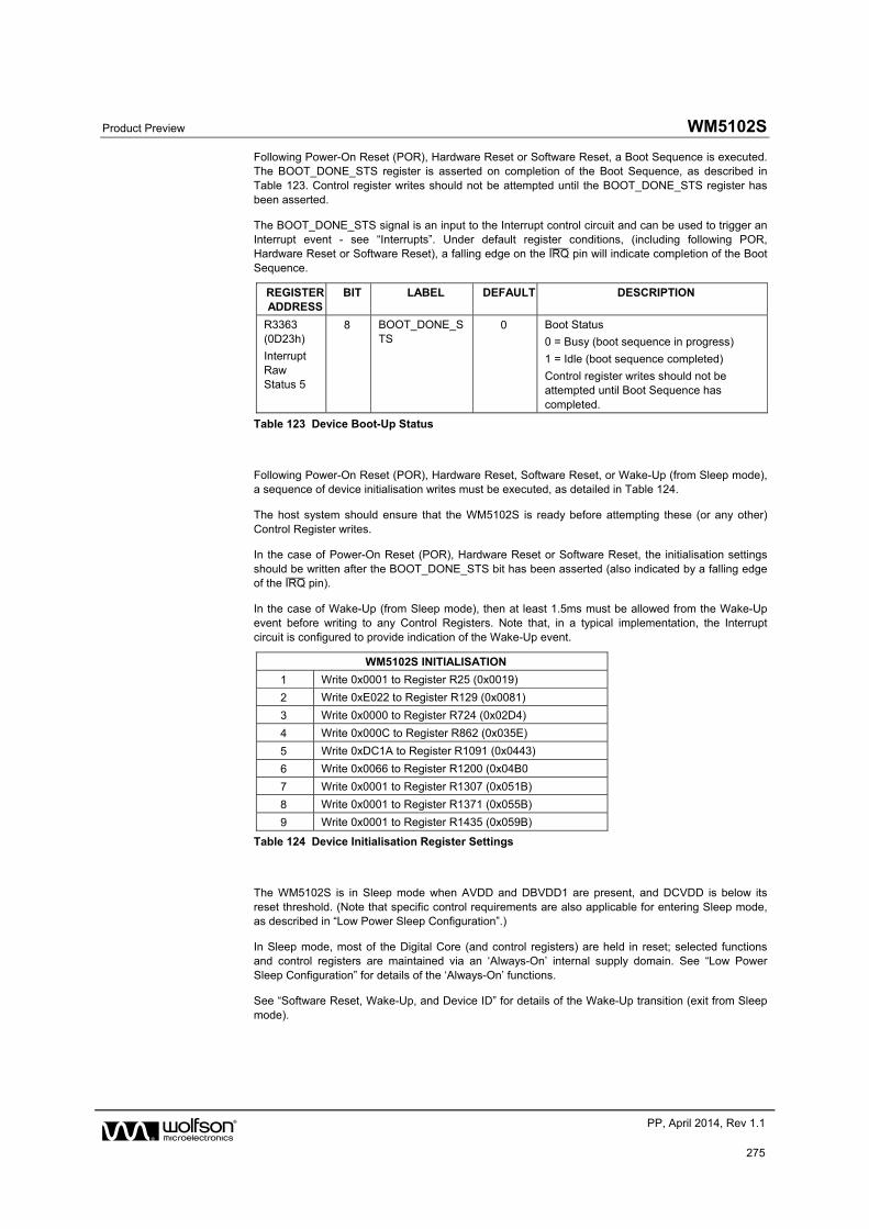
Product Preview WM5102S
w PP, April 2014, Rev 1.1
275
Following Power-On Reset (POR), Hardware Reset or Software Reset, a Boot Sequence is executed. The BOOT_DONE_STS register is asserted on completion of the Boot Sequence, as described in Table 123. Control register writes should not be attempted until the BOOT_DONE_STS register has been asserted.
The BOOT_DONE_STS signal is an input to the Interrupt control circuit and can be used to trigger an Interrupt event - see “Interrupts”. Under default register conditions, (including following POR, Hardware Reset or Software Reset), a falling edge on the IRQ¯¯¯ pin will indicate completion of the Boot Sequence.
REGISTER ADDRESS
BIT LABEL DEFAULT DESCRIPTION
R3363 (0D23h)
Interrupt Raw Status 5
8 BOOT_DONE_STS
0 Boot Status
0 = Busy (boot sequence in progress)
1 = Idle (boot sequence completed)
Control register writes should not be attempted until Boot Sequence has completed.
Table 123 Device Boot-Up Status
Following Power-On Reset (POR), Hardware Reset, Software Reset, or Wake-Up (from Sleep mode), a sequence of device initialisation writes must be executed, as detailed in Table 124.
The host system should ensure that the WM5102S is ready before attempting these (or any other) Control Register writes.
In the case of Power-On Reset (POR), Hardware Reset or Software Reset, the initialisation settings should be written after the BOOT_DONE_STS bit has been asserted (also indicated by a falling edge of the IRQ¯¯¯ pin).
In the case of Wake-Up (from Sleep mode), then at least 1.5ms must be allowed from the Wake-Up event before writing to any Control Registers. Note that, in a typical implementation, the Interrupt circuit is configured to provide indication of the Wake-Up event.
WM5102S INITIALISATION
1 Write 0x0001 to Register R25 (0x0019)
2 Write 0xE022 to Register R129 (0x0081)
3 Write 0x0000 to Register R724 (0x02D4)
4 Write 0x000C to Register R862 (0x035E)
5 Write 0xDC1A to Register R1091 (0x0443)
6 Write 0x0066 to Register R1200 (0x04B0
7 Write 0x0001 to Register R1307 (0x051B)
8 Write 0x0001 to Register R1371 (0x055B)
9 Write 0x0001 to Register R1435 (0x059B)
Table 124 Device Initialisation Register Settings
The WM5102S is in Sleep mode when AVDD and DBVDD1 are present, and DCVDD is below its reset threshold. (Note that specific control requirements are also applicable for entering Sleep mode, as described in “Low Power Sleep Configuration”.)
In Sleep mode, most of the Digital Core (and control registers) are held in reset; selected functions and control registers are maintained via an ‘Always-On’ internal supply domain. See “Low Power Sleep Configuration” for details of the ‘Always-On’ functions.
See “Software Reset, Wake-Up, and Device ID” for details of the Wake-Up transition (exit from Sleep mode).
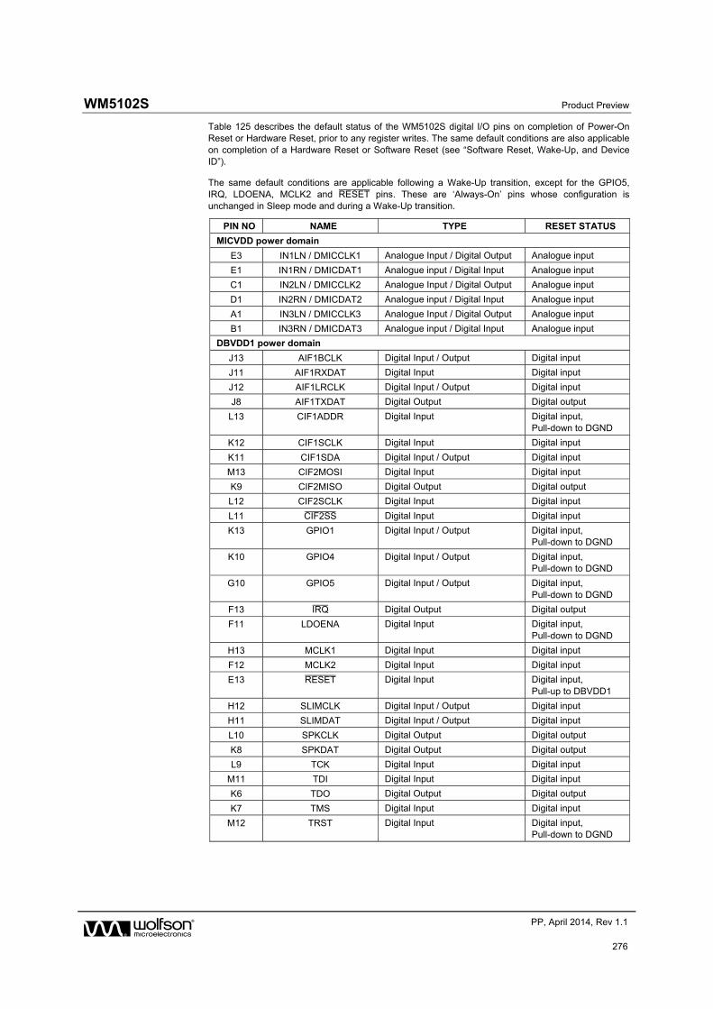
WM5102S Product Preview
w PP, April 2014, Rev 1.1
276
Table 125 describes the default status of the WM5102S digital I/O pins on completion of Power-On Reset or Hardware Reset, prior to any register writes. The same default conditions are also applicable on completion of a Hardware Reset or Software Reset (see “Software Reset, Wake-Up, and Device ID”).
The same default conditions are applicable following a Wake-Up transition, except for the GPIO5, IRQ, LDOENA, MCLK2 and RESET¯¯¯¯¯¯ pins. These are ‘Always-On’ pins whose configuration is unchanged in Sleep mode and during a Wake-Up transition.
PIN NO NAME TYPE RESET STATUS
MICVDD power domain
E3 IN1LN / DMICCLK1 Analogue Input / Digital Output Analogue input
E1 IN1RN / DMICDAT1 Analogue input / Digital Input Analogue input
C1 IN2LN / DMICCLK2 Analogue Input / Digital Output Analogue input
D1 IN2RN / DMICDAT2 Analogue input / Digital Input Analogue input
A1 IN3LN / DMICCLK3 Analogue Input / Digital Output Analogue input
B1 IN3RN / DMICDAT3 Analogue input / Digital Input Analogue input
DBVDD1 power domain
J13 AIF1BCLK Digital Input / Output Digital input
J11 AIF1RXDAT Digital Input Digital input
J12 AIF1LRCLK Digital Input / Output Digital input
J8 AIF1TXDAT Digital Output Digital output
L13 CIF1ADDR Digital Input Digital input, Pull-down to DGND
K12 CIF1SCLK Digital Input Digital input
K11 CIF1SDA Digital Input / Output Digital input
M13 CIF2MOSI Digital Input Digital input
K9 CIF2MISO Digital Output Digital output
L12 CIF2SCLK Digital Input Digital input
L11 CIF2SS¯¯¯¯¯¯ Digital Input Digital input
K13 GPIO1 Digital Input / Output Digital input, Pull-down to DGND
K10 GPIO4 Digital Input / Output Digital input, Pull-down to DGND
G10 GPIO5 Digital Input / Output Digital input, Pull-down to DGND
F13 IRQ¯¯¯ Digital Output Digital output
F11 LDOENA Digital Input Digital input, Pull-down to DGND
H13 MCLK1 Digital Input Digital input
F12 MCLK2 Digital Input Digital input
E13 RESET¯¯¯¯¯¯ Digital Input Digital input, Pull-up to DBVDD1
H12 SLIMCLK Digital Input / Output Digital input
H11 SLIMDAT Digital Input / Output Digital input
L10 SPKCLK Digital Output Digital output
K8 SPKDAT Digital Output Digital output
L9 TCK Digital Input Digital input
M11 TDI Digital Input Digital input
K6 TDO Digital Output Digital output
K7 TMS Digital Input Digital input
M12 TRST Digital Input Digital input, Pull-down to DGND
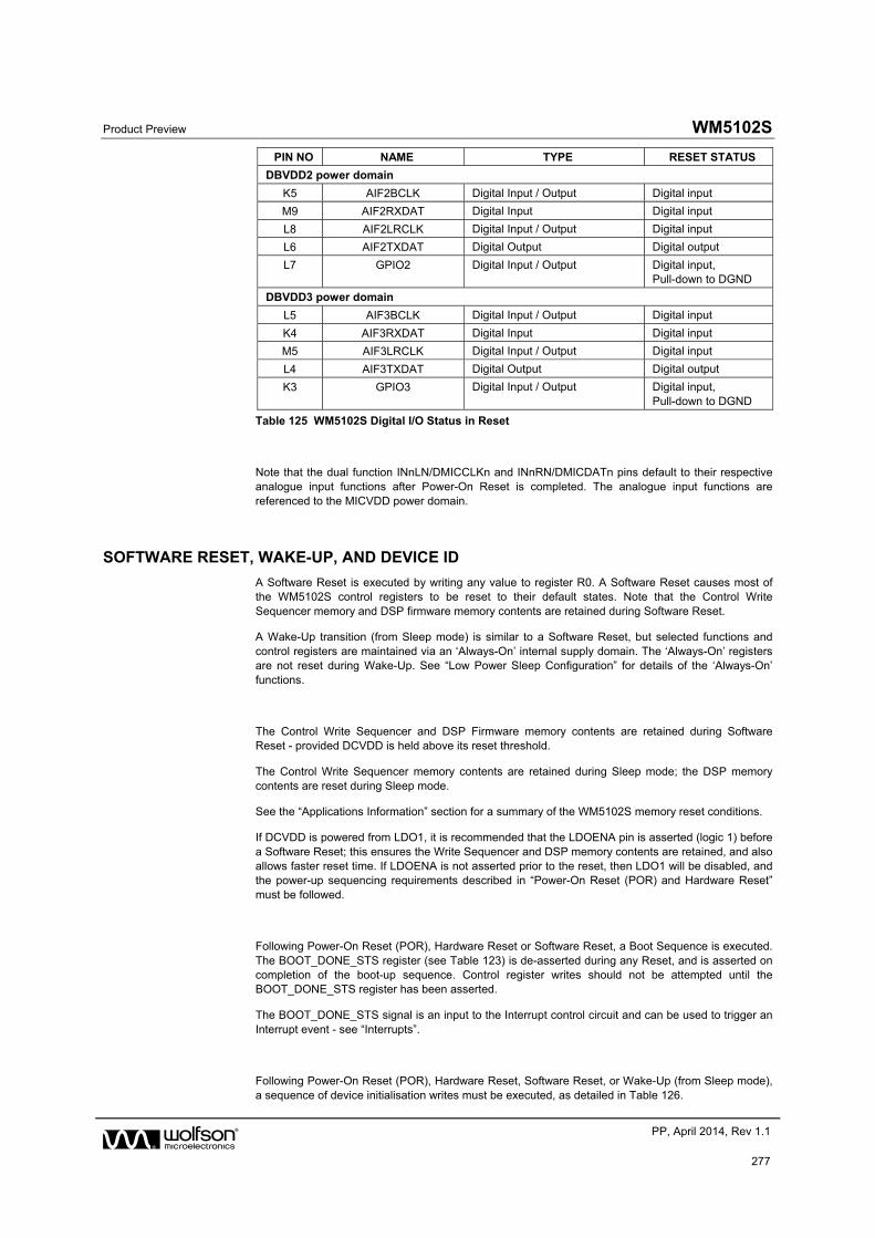
Product Preview WM5102S
w PP, April 2014, Rev 1.1
277
PIN NO NAME TYPE RESET STATUS
DBVDD2 power domain
K5 AIF2BCLK Digital Input / Output Digital input
M9 AIF2RXDAT Digital Input Digital input
L8 AIF2LRCLK Digital Input / Output Digital input
L6 AIF2TXDAT Digital Output Digital output
L7 GPIO2 Digital Input / Output Digital input, Pull-down to DGND
DBVDD3 power domain
L5 AIF3BCLK Digital Input / Output Digital input
K4 AIF3RXDAT Digital Input Digital input
M5 AIF3LRCLK Digital Input / Output Digital input
L4 AIF3TXDAT Digital Output Digital output
K3 GPIO3 Digital Input / Output Digital input, Pull-down to DGND
Table 125 WM5102S Digital I/O Status in Reset
Note that the dual function INnLN/DMICCLKn and INnRN/DMICDATn pins default to their respective analogue input functions after Power-On Reset is completed. The analogue input functions are referenced to the MICVDD power domain.
SOFTWARE RESET, WAKE-UP, AND DEVICE ID
A Software Reset is executed by writing any value to register R0. A Software Reset causes most of the WM5102S control registers to be reset to their default states. Note that the Control Write Sequencer memory and DSP firmware memory contents are retained during Software Reset.
A Wake-Up transition (from Sleep mode) is similar to a Software Reset, but selected functions and control registers are maintained via an ‘Always-On’ internal supply domain. The ‘Always-On’ registers are not reset during Wake-Up. See “Low Power Sleep Configuration” for details of the ‘Always-On’ functions.
The Control Write Sequencer and DSP Firmware memory contents are retained during Software Reset - provided DCVDD is held above its reset threshold.
The Control Write Sequencer memory contents are retained during Sleep mode; the DSP memory contents are reset during Sleep mode.
See the “Applications Information” section for a summary of the WM5102S memory reset conditions.
If DCVDD is powered from LDO1, it is recommended that the LDOENA pin is asserted (logic 1) before a Software Reset; this ensures the Write Sequencer and DSP memory contents are retained, and also allows faster reset time. If LDOENA is not asserted prior to the reset, then LDO1 will be disabled, and the power-up sequencing requirements described in “Power-On Reset (POR) and Hardware Reset” must be followed.
Following Power-On Reset (POR), Hardware Reset or Software Reset, a Boot Sequence is executed. The BOOT_DONE_STS register (see Table 123) is de-asserted during any Reset, and is asserted on completion of the boot-up sequence. Control register writes should not be attempted until the BOOT_DONE_STS register has been asserted.
The BOOT_DONE_STS signal is an input to the Interrupt control circuit and can be used to trigger an Interrupt event - see “Interrupts”.
Following Power-On Reset (POR), Hardware Reset, Software Reset, or Wake-Up (from Sleep mode), a sequence of device initialisation writes must be executed, as detailed in Table 126.
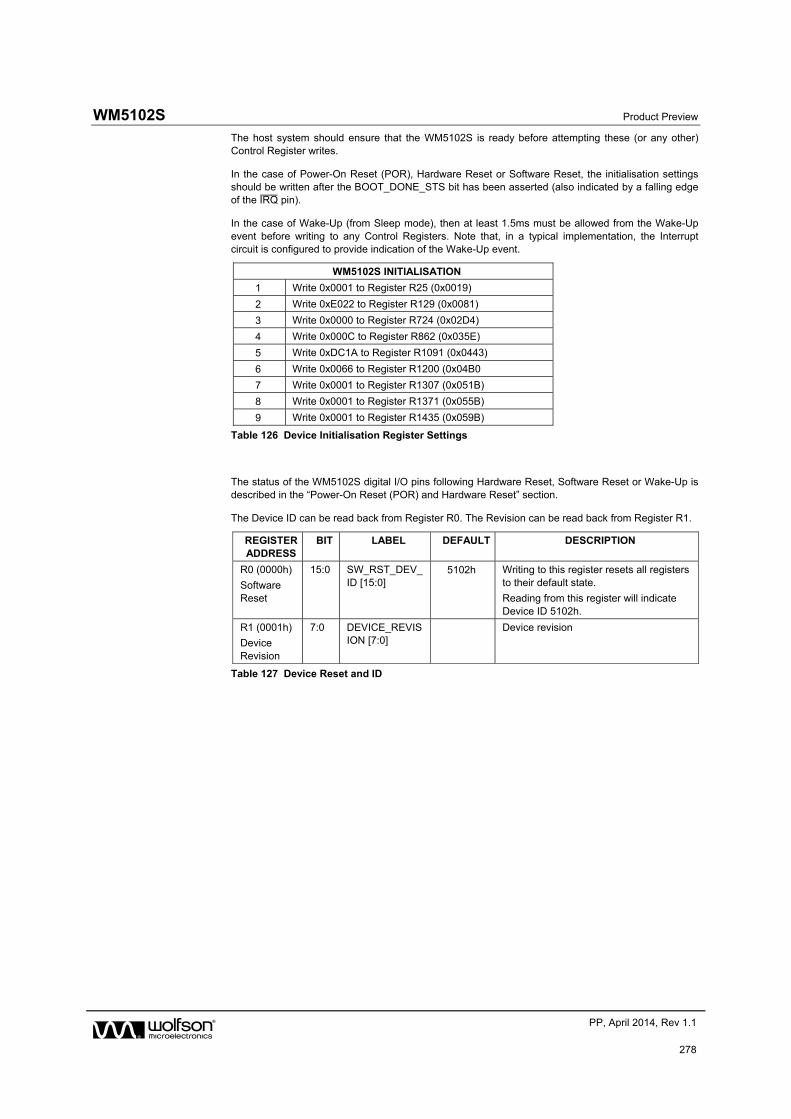
WM5102S Product Preview
w PP, April 2014, Rev 1.1
278
The host system should ensure that the WM5102S is ready before attempting these (or any other) Control Register writes.
In the case of Power-On Reset (POR), Hardware Reset or Software Reset, the initialisation settings should be written after the BOOT_DONE_STS bit has been asserted (also indicated by a falling edge of the IRQ¯¯¯ pin).
In the case of Wake-Up (from Sleep mode), then at least 1.5ms must be allowed from the Wake-Up event before writing to any Control Registers. Note that, in a typical implementation, the Interrupt circuit is configured to provide indication of the Wake-Up event.
WM5102S INITIALISATION
1 Write 0x0001 to Register R25 (0x0019)
2 Write 0xE022 to Register R129 (0x0081)
3 Write 0x0000 to Register R724 (0x02D4)
4 Write 0x000C to Register R862 (0x035E)
5 Write 0xDC1A to Register R1091 (0x0443)
6 Write 0x0066 to Register R1200 (0x04B0
7 Write 0x0001 to Register R1307 (0x051B)
8 Write 0x0001 to Register R1371 (0x055B)
9 Write 0x0001 to Register R1435 (0x059B)
Table 126 Device Initialisation Register Settings
The status of the WM5102S digital I/O pins following Hardware Reset, Software Reset or Wake-Up is described in the “Power-On Reset (POR) and Hardware Reset” section.
The Device ID can be read back from Register R0. The Revision can be read back from Register R1.
REGISTER ADDRESS
BIT LABEL DEFAULT DESCRIPTION
R0 (0000h)
Software Reset
15:0 SW_RST_DEV_ID [15:0]
5102h Writing to this register resets all registers to their default state.
Reading from this register will indicate Device ID 5102h.
R1 (0001h)
Device Revision
7:0 DEVICE_REVISION [7:0]
Device revision
Table 127 Device Reset and ID

Product Preview WM5102S
w PP, April 2014, Rev 1.1
279
REGISTER MAP
The WM5102S control registers are listed below. Note that only the register addresses described here should be accessed; writing to
other addresses may result in undefined behaviour. Register bits that are not documented should not be changed from the default
values.
REG NAME 15 14 13 12 11 10 9 8 7 6 5 4 3 2 1 0 DEFAULT
R0 (0h) Software Reset SW_RST_DEV_ID [15:0] 5102h
R1 (1h) Device Revision 0 0 0 0 0 0 0 0 DEVICE_REVISION [7:0]
R8 (8h) Ctrl IF SPI CFG 1 0 0 0 0 0 0 0 0 0 0 0 SPI_CFG
0 0 SPI_AUTO_INC [1:0]
0011h
R9 (9h) Ctrl IF I2C1 CFG 1 0 0 0 0 0 0 0 0 0 0 0 0 0 0 I2C1_AUTO_IN
C [1:0]
0001h
R22 (16h) Write Sequencer Ctrl 0
0 0 0 0 WSEQ_ABO
RT
WSEQ_STAR
T
WSEQ_ENA
WSEQ_START_INDEX [8:0] 0000h
R23 (17h) Write Sequencer Ctrl 1
0 0 0 0 0 0 WSEQ_BUS
Y
WSEQ_CURRENT_INDEX [8:0] 0000h
R24 (18h) Write Sequencer Ctrl 2
0 0 0 0 0 0 0 0 0 0 0 0 0 0 0 WSEQ
_LOAD_ME
M
0000h
R32 (20h) Tone Generator 1 0 TONE_RATE [3:0] 0 TONE_OFFSET [1:0]
0 0 TONE2_OV
D
TONE1_OV
D
0 0 TONE2_ENA
TONE1_ENA
0000h
R33 (21h) Tone Generator 2 TONE1_LVL [23:8] 1000h
R34 (22h) Tone Generator 3 0 0 0 0 0 0 0 0 TONE1_LVL [7:0] 0000h
R35 (23h) Tone Generator 4 TONE2_LVL [23:8] 1000h
R36 (24h) Tone Generator 5 0 0 0 0 0 0 0 0 TONE2_LVL [7:0] 0000h
R48 (30h) PWM Drive 1 0 PWM_RATE [3:0] PWM_CLK_SEL [2:0] 0 0 PWM2
_OVD PWM1
_OVD 0 0 PWM2
_ENA
PWM1
_ENA 0000h
R49 (31h) PWM Drive 2 0 0 0 0 0 0 PWM1_LVL [9:0] 0100h
R50 (32h) PWM Drive 3 0 0 0 0 0 0 PWM2_LVL [9:0] 0100h
R64 (40h) Wake control 0 0 0 0 0 0 0 0 WKUP_MICD_CLA
MP_FALL
WKUP_MICD_CLA
MP_RISE
WKUP_GP5_FALL
WKUP_GP5_RISE
WKUP_JD1_FALL
WKUP_JD1_RISE
0 0 0000h
R65 (41h) Sequence control 0 0 0 0 0 0 0 0 WSEQ
_ENA_MICD_CLAM
P_FALL
WSEQ
_ENA_MICD_CLAM
P_RISE
WSEQ
_ENA_GP5_F
ALL
WSEQ
_ENA_GP5_RISE
WSEQ
_ENA_JD1_F
ALL
WSEQ
_ENA_JD1_R
ISE
0 0 0000h
R97 (61h) Sample Rate
Sequence Select 1 0 0 0 0 0 0 0 WSEQ_SAMPLE_RATE_DETECT_A_INDEX [8:0] 01FFh
R98 (62h) Sample Rate Sequence Select 2
0 0 0 0 0 0 0 WSEQ_SAMPLE_RATE_DETECT_B_INDEX [8:0] 01FFh
R99 (63h) Sample Rate
Sequence Select 3 0 0 0 0 0 0 0 WSEQ_SAMPLE_RATE_DETECT_C_INDEX [8:0] 01FFh
R100 (64h) Sample Rate Sequence Select 4
0 0 0 0 0 0 0 WSEQ_SAMPLE_RATE_DETECT_D_INDEX [8:0] 01FFh
R102 (66h) Always On Triggers Sequence Select 1
0 0 0 0 0 0 0 WSEQ_MICD_CLAMP_RISE_INDEX [8:0] 01FFh
R103 (67h) Always On Triggers
Sequence Select 2 0 0 0 0 0 0 0 WSEQ_MICD_CLAMP_FALL_INDEX [8:0] 01FFh
R104 (68h) Always On Triggers Sequence Select 3
0 0 0 0 0 0 0 WSEQ_GP5_RISE_INDEX [8:0] 01FFh
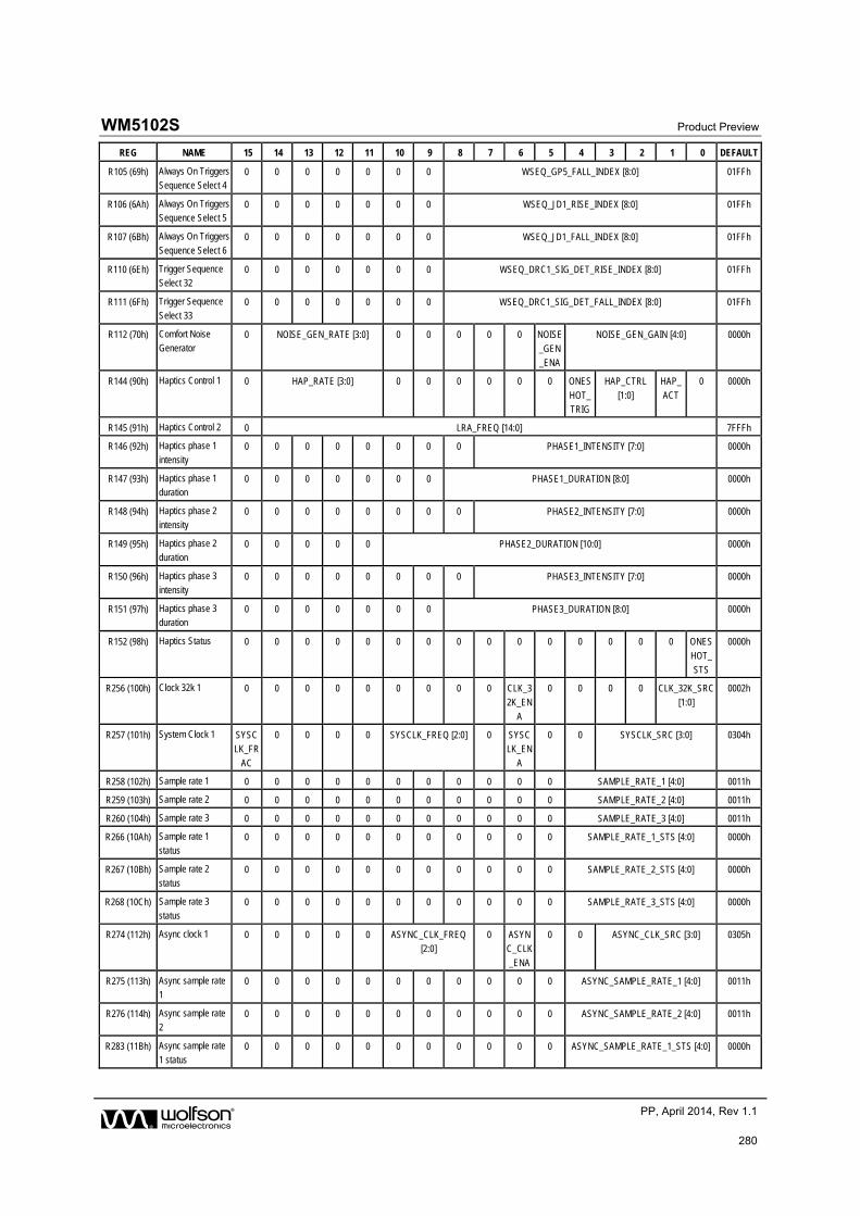
WM5102S Product Preview
w PP, April 2014, Rev 1.1
280
REG NAME 15 14 13 12 11 10 9 8 7 6 5 4 3 2 1 0 DEFAULT
R105 (69h) Always On Triggers Sequence Select 4
0 0 0 0 0 0 0 WSEQ_GP5_FALL_INDEX [8:0] 01FFh
R106 (6Ah) Always On Triggers Sequence Select 5
0 0 0 0 0 0 0 WSEQ_JD1_RISE_INDEX [8:0] 01FFh
R107 (6Bh) Always On Triggers
Sequence Select 6 0 0 0 0 0 0 0 WSEQ_JD1_FALL_INDEX [8:0] 01FFh
R110 (6Eh) Trigger Sequence Select 32
0 0 0 0 0 0 0 WSEQ_DRC1_SIG_DET_RISE_INDEX [8:0] 01FFh
R111 (6Fh) Trigger Sequence
Select 33 0 0 0 0 0 0 0 WSEQ_DRC1_SIG_DET_FALL_INDEX [8:0] 01FFh
R112 (70h) Comfort Noise Generator
0 NOISE_GEN_RATE [3:0] 0 0 0 0 0 NOISE
_GEN_ENA
NOISE_GEN_GAIN [4:0] 0000h
R144 (90h) Haptics Control 1 0 HAP_RATE [3:0] 0 0 0 0 0 0 ONES
HOT_TRIG
HAP_CTRL
[1:0]
HAP_
ACT
0 0000h
R145 (91h) Haptics Control 2 0 LRA_FREQ [14:0] 7FFFh
R146 (92h) Haptics phase 1
intensity 0 0 0 0 0 0 0 0 PHASE1_INTENSITY [7:0] 0000h
R147 (93h) Haptics phase 1 duration
0 0 0 0 0 0 0 PHASE1_DURATION [8:0] 0000h
R148 (94h) Haptics phase 2 intensity
0 0 0 0 0 0 0 0 PHASE2_INTENSITY [7:0] 0000h
R149 (95h) Haptics phase 2
duration 0 0 0 0 0 PHASE2_DURATION [10:0] 0000h
R150 (96h) Haptics phase 3 intensity
0 0 0 0 0 0 0 0 PHASE3_INTENSITY [7:0] 0000h
R151 (97h) Haptics phase 3 duration
0 0 0 0 0 0 0 PHASE3_DURATION [8:0] 0000h
R152 (98h) Haptics Status 0 0 0 0 0 0 0 0 0 0 0 0 0 0 0 ONES
HOT_STS
0000h
R256 (100h) Clock 32k 1 0 0 0 0 0 0 0 0 0 CLK_32K_EN
A
0 0 0 0 CLK_32K_SRC [1:0]
0002h
R257 (101h) System Clock 1 SYSCLK_FR
AC
0 0 0 0 SYSCLK_FREQ [2:0] 0 SYSCLK_EN
A
0 0 SYSCLK_SRC [3:0] 0304h
R258 (102h) Sample rate 1 0 0 0 0 0 0 0 0 0 0 0 SAMPLE_RATE_1 [4:0] 0011h
R259 (103h) Sample rate 2 0 0 0 0 0 0 0 0 0 0 0 SAMPLE_RATE_2 [4:0] 0011h
R260 (104h) Sample rate 3 0 0 0 0 0 0 0 0 0 0 0 SAMPLE_RATE_3 [4:0] 0011h
R266 (10Ah) Sample rate 1 status
0 0 0 0 0 0 0 0 0 0 0 SAMPLE_RATE_1_STS [4:0] 0000h
R267 (10Bh) Sample rate 2
status 0 0 0 0 0 0 0 0 0 0 0 SAMPLE_RATE_2_STS [4:0] 0000h
R268 (10Ch) Sample rate 3 status
0 0 0 0 0 0 0 0 0 0 0 SAMPLE_RATE_3_STS [4:0] 0000h
R274 (112h) Async clock 1 0 0 0 0 0 ASYNC_CLK_FREQ [2:0]
0 ASYNC_CLK
_ENA
0 0 ASYNC_CLK_SRC [3:0] 0305h
R275 (113h) Async sample rate 1
0 0 0 0 0 0 0 0 0 0 0 ASYNC_SAMPLE_RATE_1 [4:0] 0011h
R276 (114h) Async sample rate 2
0 0 0 0 0 0 0 0 0 0 0 ASYNC_SAMPLE_RATE_2 [4:0] 0011h
R283 (11Bh) Async sample rate
1 status 0 0 0 0 0 0 0 0 0 0 0 ASYNC_SAMPLE_RATE_1_STS [4:0] 0000h

Product Preview WM5102S
w PP, April 2014, Rev 1.1
281
REG NAME 15 14 13 12 11 10 9 8 7 6 5 4 3 2 1 0 DEFAULT
R284 (11Bh) Async sample rate 2 status
0 0 0 0 0 0 0 0 0 0 0 ASYNC_SAMPLE_RATE_2_STS [4:0] 0000h
R329 (149h) Output system
clock OPCLK_EN
A
0 0 0 0 0 0 0 OPCLK_DIV [4:0] OPCLK_SEL [2:0] 0000h
R330 (14Ah) Output async clock OPCLK_ASY
NC_ENA
0 0 0 0 0 0 0 OPCLK_ASYNC_DIV [4:0] OPCLK_ASYNC_SEL [2:0]
0000h
R338 (152h) Rate Estimator 1 0 0 0 0 0 0 0 0 0 0 0 TRIG_ON_S
TARTUP
LRCLK_SRC [2:0] RATE_EST_E
NA
0000h
R339 (153h) Rate Estimator 2 0 0 0 0 0 0 0 0 0 0 0 SAMPLE_RATE_DETECT_A [4:0] 0000h
R340 (154h) Rate Estimator 3 0 0 0 0 0 0 0 0 0 0 0 SAMPLE_RATE_DETECT_B [4:0] 0000h
R341 (155h) Rate Estimator 4 0 0 0 0 0 0 0 0 0 0 0 SAMPLE_RATE_DETECT_C [4:0] 0000h
R342 (156h) Rate Estimator 5 0 0 0 0 0 0 0 0 0 0 0 SAMPLE_RATE_DETECT_D [4:0] 0000h
R353 (161h) Dynamic
Frequency Scaling 1
0 0 0 0 0 0 0 0 0 0 0 0 0 0 0 SUBSYS_M
AX_FREQ
0000h
R369 (171h) FLL1 Control 1 0 0 0 0 0 0 0 0 0 0 0 0 0 0 FLL1_
FREERUN
FLL1_
ENA
0002h
R370 (172h) FLL1 Control 2 FLL1_CTRL_
UPD
0 0 0 0 0 FLL1_N [9:0] 0008h
R371 (173h) FLL1 Control 3 FLL1_THETA [15:0] 0018h
R372 (174h) FLL1 Control 4 FLL1_LAMBDA [15:0] 007Dh
R373 (175h) FLL1 Control 5 0 0 0 0 0 FLL1_FRATIO [2:0] 0 0 0 0 FLL1_OUTDIV [2:0] 0 0004h
R374 (176h) FLL1 Control 6 0 0 0 0 0 0 0 0 FLL1_REFCLK_DIV [1:0]
0 0 FLL1_REFCLK_SRC [3:0] 0000h
R377 (179h) FLL1 Control 7 0 0 0 0 0 0 0 0 0 0 FLL1_GAIN [3:0] 0 0 0000h
R385 (181h) FLL1 Synchroniser
1 0 0 0 0 0 0 0 0 0 0 0 0 0 0 0 FLL1_
SYNC_ENA
0000h
R386 (182h) FLL1 Synchroniser 2
0 0 0 0 0 0 FLL1_SYNC_N [9:0] 0000h
R387 (183h) FLL1 Synchroniser
3 FLL1_SYNC_THETA [15:0] 0000h
R388 (184h) FLL1 Synchroniser 4
FLL1_SYNC_LAMBDA [15:0] 0000h
R389 (185h) FLL1 Synchroniser
5 0 0 0 0 0 FLL1_SYNC_FRATIO
[2:0] 0 0 0 0 0 0 0 0 0000h
R390 (186h) FLL1 Synchroniser 6
0 0 0 0 0 0 0 0 FLL1_SYNCCL
K_DIV [1:0]
0 0 FLL1_SYNCCLK_SRC [3:0] 0000h
R391 (187h) FLL1 Synchroniser 7
0 0 0 0 0 0 0 0 0 0 FLL1_SYNC_GAIN [3:0] 0 FLL1_SYNC
_DFSAT
0001h
R393 (189h) FLL1 Spread
Spectrum 0 0 0 0 0 0 0 0 0 0 FLL1_SS_AMP
L [1:0] FLL1_SS_FRE
Q [1:0] FLL1_SS_SEL
[1:0] 0000h
R394 (18Ah) FLL1 GPIO Clock 0 0 0 0 0 0 0 0 FLL1_GPCLK_DIV [6:0] FLL1_
GPCLK_EN
A
0004h
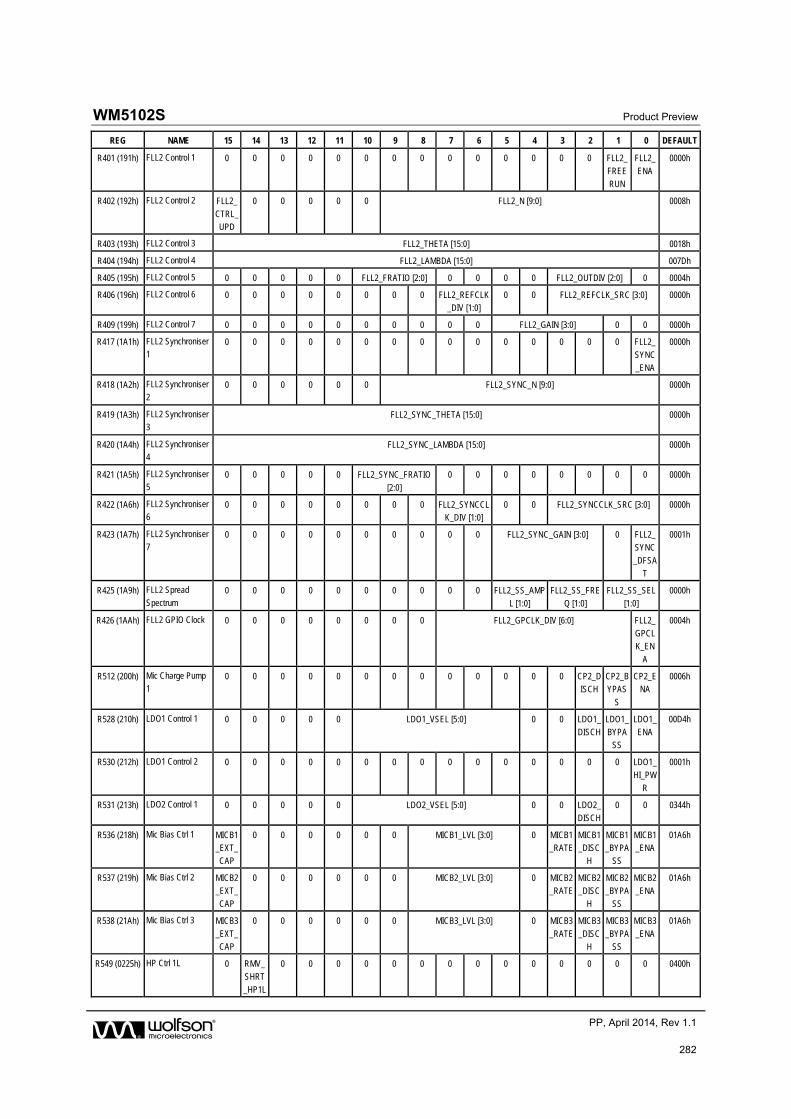
WM5102S Product Preview
w PP, April 2014, Rev 1.1
282
REG NAME 15 14 13 12 11 10 9 8 7 6 5 4 3 2 1 0 DEFAULT
R401 (191h) FLL2 Control 1 0 0 0 0 0 0 0 0 0 0 0 0 0 0 FLL2_
FREERUN
FLL2_
ENA
0000h
R402 (192h) FLL2 Control 2 FLL2_
CTRL_UPD
0 0 0 0 0 FLL2_N [9:0] 0008h
R403 (193h) FLL2 Control 3 FLL2_THETA [15:0] 0018h
R404 (194h) FLL2 Control 4 FLL2_LAMBDA [15:0] 007Dh
R405 (195h) FLL2 Control 5 0 0 0 0 0 FLL2_FRATIO [2:0] 0 0 0 0 FLL2_OUTDIV [2:0] 0 0004h
R406 (196h) FLL2 Control 6 0 0 0 0 0 0 0 0 FLL2_REFCLK_DIV [1:0]
0 0 FLL2_REFCLK_SRC [3:0] 0000h
R409 (199h) FLL2 Control 7 0 0 0 0 0 0 0 0 0 0 FLL2_GAIN [3:0] 0 0 0000h
R417 (1A1h) FLL2 Synchroniser 1
0 0 0 0 0 0 0 0 0 0 0 0 0 0 0 FLL2_
SYNC_ENA
0000h
R418 (1A2h) FLL2 Synchroniser
2 0 0 0 0 0 0 FLL2_SYNC_N [9:0] 0000h
R419 (1A3h) FLL2 Synchroniser 3
FLL2_SYNC_THETA [15:0] 0000h
R420 (1A4h) FLL2 Synchroniser 4
FLL2_SYNC_LAMBDA [15:0] 0000h
R421 (1A5h) FLL2 Synchroniser
5 0 0 0 0 0 FLL2_SYNC_FRATIO
[2:0]
0 0 0 0 0 0 0 0 0000h
R422 (1A6h) FLL2 Synchroniser 6
0 0 0 0 0 0 0 0 FLL2_SYNCCLK_DIV [1:0]
0 0 FLL2_SYNCCLK_SRC [3:0] 0000h
R423 (1A7h) FLL2 Synchroniser
7 0 0 0 0 0 0 0 0 0 0 FLL2_SYNC_GAIN [3:0] 0 FLL2_
SYNC
_DFSAT
0001h
R425 (1A9h) FLL2 Spread
Spectrum 0 0 0 0 0 0 0 0 0 0 FLL2_SS_AMP
L [1:0]
FLL2_SS_FRE
Q [1:0]
FLL2_SS_SEL
[1:0]
0000h
R426 (1AAh) FLL2 GPIO Clock 0 0 0 0 0 0 0 0 FLL2_GPCLK_DIV [6:0] FLL2_GPCLK_EN
A
0004h
R512 (200h) Mic Charge Pump 1
0 0 0 0 0 0 0 0 0 0 0 0 0 CP2_DISCH
CP2_BYPAS
S
CP2_ENA
0006h
R528 (210h) LDO1 Control 1 0 0 0 0 0 LDO1_VSEL [5:0] 0 0 LDO1_DISCH
LDO1_BYPA
SS
LDO1_ENA
00D4h
R530 (212h) LDO1 Control 2 0 0 0 0 0 0 0 0 0 0 0 0 0 0 0 LDO1_
HI_PWR
0001h
R531 (213h) LDO2 Control 1 0 0 0 0 0 LDO2_VSEL [5:0] 0 0 LDO2_
DISCH
0 0 0344h
R536 (218h) Mic Bias Ctrl 1 MICB1_EXT_CAP
0 0 0 0 0 0 MICB1_LVL [3:0] 0 MICB1_RATE
MICB1_DISC
H
MICB1_BYPA
SS
MICB1_ENA
01A6h
R537 (219h) Mic Bias Ctrl 2 MICB2
_EXT_CAP
0 0 0 0 0 0 MICB2_LVL [3:0] 0 MICB2
_RATE MICB2
_DISCH
MICB2
_BYPASS
MICB2
_ENA 01A6h
R538 (21Ah) Mic Bias Ctrl 3 MICB3
_EXT_CAP
0 0 0 0 0 0 MICB3_LVL [3:0] 0 MICB3
_RATE
MICB3
_DISCH
MICB3
_BYPASS
MICB3
_ENA
01A6h
R549 (0225h) HP Ctrl 1L 0 RMV_SHRT
_HP1L
0 0 0 0 0 0 0 0 0 0 0 0 0 0 0400h
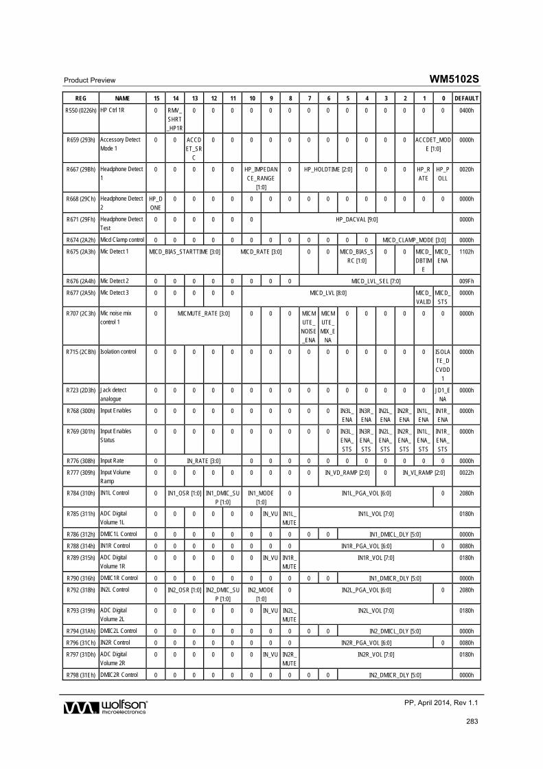
Product Preview WM5102S
w PP, April 2014, Rev 1.1
283
REG NAME 15 14 13 12 11 10 9 8 7 6 5 4 3 2 1 0 DEFAULT
R550 (0226h) HP Ctrl 1R 0 RMV_SHRT_HP1R
0 0 0 0 0 0 0 0 0 0 0 0 0 0 0400h
R659 (293h) Accessory Detect Mode 1
0 0 ACCD
ET_SRC
0 0 0 0 0 0 0 0 0 0 0 ACCDET_MOD
E [1:0]
0000h
R667 (29Bh) Headphone Detect
1 0 0 0 0 0 HP_IMPEDAN
CE_RANGE [1:0]
0 HP_HOLDTIME [2:0] 0 0 0 HP_R
ATE
HP_P
OLL
0020h
R668 (29Ch) Headphone Detect
2 HP_DONE
0 0 0 0 0 0 0 0 0 0 0 0 0 0 0 0000h
R671 (29Fh) Headphone Detect
Test 0 0 0 0 0 0 HP_DACVAL [9:0] 0000h
R674 (2A2h) Micd Clamp control 0 0 0 0 0 0 0 0 0 0 0 0 MICD_CLAMP_MODE [3:0] 0000h
R675 (2A3h) Mic Detect 1 MICD_BIAS_STARTTIME [3:0] MICD_RATE [3:0] 0 0 MICD_BIAS_SRC [1:0]
0 0 MICD_DBTIM
E
MICD_ENA
1102h
R676 (2A4h) Mic Detect 2 0 0 0 0 0 0 0 0 MICD_LVL_SEL [7:0] 009Fh
R677 (2A5h) Mic Detect 3 0 0 0 0 0 MICD_LVL [8:0] MICD_
VALID
MICD_
STS
0000h
R707 (2C3h) Mic noise mix control 1
0 MICMUTE_RATE [3:0] 0 0 0 MICMUTE_
NOISE_ENA
MICMUTE_
MIX_ENA
0 0 0 0 0 0 0000h
R715 (2CBh) Isolation control 0 0 0 0 0 0 0 0 0 0 0 0 0 0 0 ISOLATE_D
CVDD1
0000h
R723 (2D3h) Jack detect
analogue 0 0 0 0 0 0 0 0 0 0 0 0 0 0 0 JD1_E
NA
0000h
R768 (300h) Input Enables 0 0 0 0 0 0 0 0 0 0 IN3L_ENA
IN3R_ENA
IN2L_ENA
IN2R_ENA
IN1L_ENA
IN1R_ENA
0000h
R769 (301h) Input Enables
Status 0 0 0 0 0 0 0 0 0 0 IN3L_
ENA_
STS
IN3R_ENA_
STS
IN2L_ENA_
STS
IN2R_ENA_
STS
IN1L_ENA_
STS
IN1R_ENA_
STS
0000h
R776 (308h) Input Rate 0 IN_RATE [3:0] 0 0 0 0 0 0 0 0 0 0 0 0000h
R777 (309h) Input Volume Ramp
0 0 0 0 0 0 0 0 0 IN_VD_RAMP [2:0] 0 IN_VI_RAMP [2:0] 0022h
R784 (310h) IN1L Control 0 IN1_OSR [1:0] IN1_DMIC_SU
P [1:0]
IN1_MODE
[1:0]
0 IN1L_PGA_VOL [6:0] 0 2080h
R785 (311h) ADC Digital Volume 1L
0 0 0 0 0 0 IN_VU IN1L_MUTE
IN1L_VOL [7:0] 0180h
R786 (312h) DMIC1L Control 0 0 0 0 0 0 0 0 0 0 IN1_DMICL_DLY [5:0] 0000h
R788 (314h) IN1R Control 0 0 0 0 0 0 0 0 IN1R_PGA_VOL [6:0] 0 0080h
R789 (315h) ADC Digital Volume 1R
0 0 0 0 0 0 IN_VU IN1R_MUTE
IN1R_VOL [7:0] 0180h
R790 (316h) DMIC1R Control 0 0 0 0 0 0 0 0 0 0 IN1_DMICR_DLY [5:0] 0000h
R792 (318h) IN2L Control 0 IN2_OSR [1:0] IN2_DMIC_SU
P [1:0]
IN2_MODE
[1:0]
0 IN2L_PGA_VOL [6:0] 0 2080h
R793 (319h) ADC Digital Volume 2L
0 0 0 0 0 0 IN_VU IN2L_MUTE
IN2L_VOL [7:0] 0180h
R794 (31Ah) DMIC2L Control 0 0 0 0 0 0 0 0 0 0 IN2_DMICL_DLY [5:0] 0000h
R796 (31Ch) IN2R Control 0 0 0 0 0 0 0 0 IN2R_PGA_VOL [6:0] 0 0080h
R797 (31Dh) ADC Digital
Volume 2R 0 0 0 0 0 0 IN_VU IN2R_
MUTE IN2R_VOL [7:0] 0180h
R798 (31Eh) DMIC2R Control 0 0 0 0 0 0 0 0 0 0 IN2_DMICR_DLY [5:0] 0000h
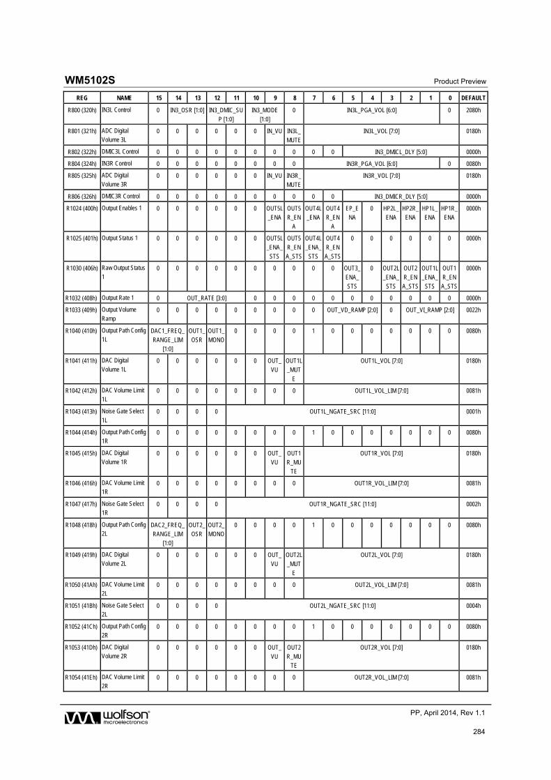
WM5102S Product Preview
w PP, April 2014, Rev 1.1
284
REG NAME 15 14 13 12 11 10 9 8 7 6 5 4 3 2 1 0 DEFAULT
R800 (320h) IN3L Control 0 IN3_OSR [1:0] IN3_DMIC_SU
P [1:0]
IN3_MODE
[1:0]
0 IN3L_PGA_VOL [6:0] 0 2080h
R801 (321h) ADC Digital Volume 3L
0 0 0 0 0 0 IN_VU IN3L_MUTE
IN3L_VOL [7:0] 0180h
R802 (322h) DMIC3L Control 0 0 0 0 0 0 0 0 0 0 IN3_DMICL_DLY [5:0] 0000h
R804 (324h) IN3R Control 0 0 0 0 0 0 0 0 IN3R_PGA_VOL [6:0] 0 0080h
R805 (325h) ADC Digital
Volume 3R 0 0 0 0 0 0 IN_VU IN3R_
MUTE
IN3R_VOL [7:0] 0180h
R806 (326h) DMIC3R Control 0 0 0 0 0 0 0 0 0 0 IN3_DMICR_DLY [5:0] 0000h
R1024 (400h) Output Enables 1 0 0 0 0 0 0 OUT5L_ENA
OUT5R_EN
A
OUT4L_ENA
OUT4R_EN
A
EP_ENA
0 HP2L_ENA
HP2R_ENA
HP1L_ENA
HP1R_ENA
0000h
R1025 (401h) Output Status 1 0 0 0 0 0 0 OUT5L
_ENA_STS
OUT5
R_ENA_STS
OUT4L
_ENA_STS
OUT4
R_ENA_STS
0 0 0 0 0 0 0000h
R1030 (406h) Raw Output Status
1 0 0 0 0 0 0 0 0 0 0 OUT3_
ENA_STS
0 OUT2L
_ENA_STS
OUT2
R_ENA_STS
OUT1L
_ENA_STS
OUT1
R_ENA_STS
0000h
R1032 (408h) Output Rate 1 0 OUT_RATE [3:0] 0 0 0 0 0 0 0 0 0 0 0 0000h
R1033 (409h) Output Volume Ramp
0 0 0 0 0 0 0 0 0 OUT_VD_RAMP [2:0] 0 OUT_VI_RAMP [2:0] 0022h
R1040 (410h) Output Path Config
1L DAC1_FREQ_
RANGE_LIM [1:0]
OUT1_
OSR
OUT1_
MONO
0 0 0 0 1 0 0 0 0 0 0 0 0080h
R1041 (411h) DAC Digital
Volume 1L 0 0 0 0 0 0 OUT_
VU OUT1L_MUT
E
OUT1L_VOL [7:0] 0180h
R1042 (412h) DAC Volume Limit 1L
0 0 0 0 0 0 0 0 OUT1L_VOL_LIM [7:0] 0081h
R1043 (413h) Noise Gate Select
1L 0 0 0 0 OUT1L_NGATE_SRC [11:0] 0001h
R1044 (414h) Output Path Config 1R
0 0 0 0 0 0 0 0 1 0 0 0 0 0 0 0 0080h
R1045 (415h) DAC Digital
Volume 1R 0 0 0 0 0 0 OUT_
VU OUT1R_MU
TE
OUT1R_VOL [7:0] 0180h
R1046 (416h) DAC Volume Limit 1R
0 0 0 0 0 0 0 0 OUT1R_VOL_LIM [7:0] 0081h
R1047 (417h) Noise Gate Select
1R 0 0 0 0 OUT1R_NGATE_SRC [11:0] 0002h
R1048 (418h) Output Path Config 2L
DAC2_FREQ_RANGE_LIM
[1:0]
OUT2_OSR
OUT2_MONO
0 0 0 0 1 0 0 0 0 0 0 0 0080h
R1049 (419h) DAC Digital Volume 2L
0 0 0 0 0 0 OUT_
VU
OUT2L
_MUTE
OUT2L_VOL [7:0] 0180h
R1050 (41Ah) DAC Volume Limit
2L 0 0 0 0 0 0 0 0 OUT2L_VOL_LIM [7:0] 0081h
R1051 (41Bh) Noise Gate Select 2L
0 0 0 0 OUT2L_NGATE_SRC [11:0] 0004h
R1052 (41Ch) Output Path Config
2R 0 0 0 0 0 0 0 0 1 0 0 0 0 0 0 0 0080h
R1053 (41Dh) DAC Digital Volume 2R
0 0 0 0 0 0 OUT_
VU
OUT2
R_MUTE
OUT2R_VOL [7:0] 0180h
R1054 (41Eh) DAC Volume Limit
2R 0 0 0 0 0 0 0 0 OUT2R_VOL_LIM [7:0] 0081h
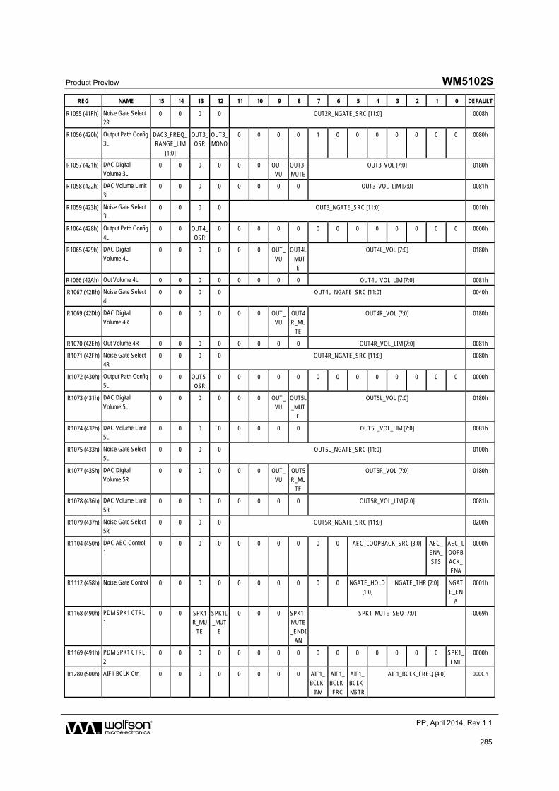
Product Preview WM5102S
w PP, April 2014, Rev 1.1
285
REG NAME 15 14 13 12 11 10 9 8 7 6 5 4 3 2 1 0 DEFAULT
R1055 (41Fh) Noise Gate Select 2R
0 0 0 0 OUT2R_NGATE_SRC [11:0] 0008h
R1056 (420h) Output Path Config
3L DAC3_FREQ_RANGE_LIM
[1:0]
OUT3_OSR
OUT3_MONO
0 0 0 0 1 0 0 0 0 0 0 0 0080h
R1057 (421h) DAC Digital Volume 3L
0 0 0 0 0 0 OUT_VU
OUT3_MUTE
OUT3_VOL [7:0] 0180h
R1058 (422h) DAC Volume Limit
3L 0 0 0 0 0 0 0 0 OUT3_VOL_LIM [7:0] 0081h
R1059 (423h) Noise Gate Select 3L
0 0 0 0 OUT3_NGATE_SRC [11:0] 0010h
R1064 (428h) Output Path Config 4L
0 0 OUT4_OSR
0 0 0 0 0 0 0 0 0 0 0 0 0 0000h
R1065 (429h) DAC Digital
Volume 4L 0 0 0 0 0 0 OUT_
VU
OUT4L
_MUTE
OUT4L_VOL [7:0] 0180h
R1066 (42Ah) Out Volume 4L 0 0 0 0 0 0 0 0 OUT4L_VOL_LIM [7:0] 0081h
R1067 (42Bh) Noise Gate Select
4L 0 0 0 0 OUT4L_NGATE_SRC [11:0] 0040h
R1069 (42Dh) DAC Digital Volume 4R
0 0 0 0 0 0 OUT_
VU
OUT4
R_MUTE
OUT4R_VOL [7:0] 0180h
R1070 (42Eh) Out Volume 4R 0 0 0 0 0 0 0 0 OUT4R_VOL_LIM [7:0] 0081h
R1071 (42Fh) Noise Gate Select
4R 0 0 0 0 OUT4R_NGATE_SRC [11:0] 0080h
R1072 (430h) Output Path Config 5L
0 0 OUT5_OSR
0 0 0 0 0 0 0 0 0 0 0 0 0 0000h
R1073 (431h) DAC Digital
Volume 5L 0 0 0 0 0 0 OUT_
VU OUT5L_MUT
E
OUT5L_VOL [7:0] 0180h
R1074 (432h) DAC Volume Limit 5L
0 0 0 0 0 0 0 0 OUT5L_VOL_LIM [7:0] 0081h
R1075 (433h) Noise Gate Select
5L 0 0 0 0 OUT5L_NGATE_SRC [11:0] 0100h
R1077 (435h) DAC Digital Volume 5R
0 0 0 0 0 0 OUT_VU
OUT5R_MU
TE
OUT5R_VOL [7:0] 0180h
R1078 (436h) DAC Volume Limit
5R 0 0 0 0 0 0 0 0 OUT5R_VOL_LIM [7:0] 0081h
R1079 (437h) Noise Gate Select 5R
0 0 0 0 OUT5R_NGATE_SRC [11:0] 0200h
R1104 (450h) DAC AEC Control
1 0 0 0 0 0 0 0 0 0 0 AEC_LOOPBACK_SRC [3:0] AEC_
ENA_
STS
AEC_LOOPB
ACK_ENA
0000h
R1112 (458h) Noise Gate Control 0 0 0 0 0 0 0 0 0 0 NGATE_HOLD
[1:0]
NGATE_THR [2:0] NGAT
E_ENA
0001h
R1168 (490h) PDM SPK1 CTRL
1 0 0 SPK1
R_MU
TE
SPK1L_MUT
E
0 0 0 SPK1_MUTE
_ENDIAN
SPK1_MUTE_SEQ [7:0] 0069h
R1169 (491h) PDM SPK1 CTRL
2 0 0 0 0 0 0 0 0 0 0 0 0 0 0 0 SPK1_
FMT
0000h
R1280 (500h) AIF1 BCLK Ctrl 0 0 0 0 0 0 0 0 AIF1_BCLK_
INV
AIF1_BCLK_FRC
AIF1_BCLK_MSTR
AIF1_BCLK_FREQ [4:0] 000Ch
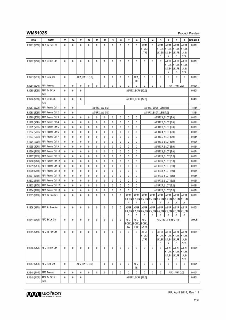
WM5102S Product Preview
w PP, April 2014, Rev 1.1
286
REG NAME 15 14 13 12 11 10 9 8 7 6 5 4 3 2 1 0 DEFAULT
R1281 (501h) AIF1 Tx Pin Ctrl 0 0 0 0 0 0 0 0 0 0 AIF1T
X_DAT_TRI
0 AIF1T
X_LRCLK_SR
C
AIF1T
X_LRCLK_IN
V
AIF1T
X_LRCLK_FR
C
AIF1T
X_LRCLK_M
STR
0008h
R1282 (502h) AIF1 Rx Pin Ctrl 0 0 0 0 0 0 0 0 0 0 0 0 0 AIF1RX_LRCLK_IN
V
AIF1RX_LRCLK_FR
C
AIF1RX_LRCLK_M
STR
0000h
R1283 (503h) AIF1 Rate Ctrl 0 AIF1_RATE [3:0] 0 0 0 0 AIF1_TRI
0 0 0 0 0 0 0000h
R1284 (504h) AIF1 Format 0 0 0 0 0 0 0 0 0 0 0 0 0 AIF1_FMT [2:0] 0000h
R1285 (505h) AIF1 Tx BCLK
Rate 0 0 0 AIF1TX_BCPF [12:0] 0040h
R1286 (506h) AIF1 Rx BCLK Rate
0 0 0 AIF1RX_BCPF [12:0] 0040h
R1287 (507h) AIF1 Frame Ctrl 1 0 0 AIF1TX_WL [5:0] AIF1TX_SLOT_LEN [7:0] 1818h
R1288 (508h) AIF1 Frame Ctrl 2 0 0 AIF1RX_WL [5:0] AIF1RX_SLOT_LEN [7:0] 1818h
R1289 (509h) AIF1 Frame Ctrl 3 0 0 0 0 0 0 0 0 0 0 AIF1TX1_SLOT [5:0] 0000h
R1290 (50Ah) AIF1 Frame Ctrl 4 0 0 0 0 0 0 0 0 0 0 AIF1TX2_SLOT [5:0] 0001h
R1291 (50Bh) AIF1 Frame Ctrl 5 0 0 0 0 0 0 0 0 0 0 AIF1TX3_SLOT [5:0] 0002h
R1292 (50Ch) AIF1 Frame Ctrl 6 0 0 0 0 0 0 0 0 0 0 AIF1TX4_SLOT [5:0] 0003h
R1293 (50Dh) AIF1 Frame Ctrl 7 0 0 0 0 0 0 0 0 0 0 AIF1TX5_SLOT [5:0] 0004h
R1294 (50Eh) AIF1 Frame Ctrl 8 0 0 0 0 0 0 0 0 0 0 AIF1TX6_SLOT [5:0] 0005h
R1295 (50Fh) AIF1 Frame Ctrl 9 0 0 0 0 0 0 0 0 0 0 AIF1TX7_SLOT [5:0] 0006h
R1296 (510h) AIF1 Frame Ctrl 10 0 0 0 0 0 0 0 0 0 0 AIF1TX8_SLOT [5:0] 0007h
R1297 (511h) AIF1 Frame Ctrl 11 0 0 0 0 0 0 0 0 0 0 AIF1RX1_SLOT [5:0] 0000h
R1298 (512h) AIF1 Frame Ctrl 12 0 0 0 0 0 0 0 0 0 0 AIF1RX2_SLOT [5:0] 0001h
R1299 (513h) AIF1 Frame Ctrl 13 0 0 0 0 0 0 0 0 0 0 AIF1RX3_SLOT [5:0] 0002h
R1300 (514h) AIF1 Frame Ctrl 14 0 0 0 0 0 0 0 0 0 0 AIF1RX4_SLOT [5:0] 0003h
R1301 (515h) AIF1 Frame Ctrl 15 0 0 0 0 0 0 0 0 0 0 AIF1RX5_SLOT [5:0] 0004h
R1302 (516h) AIF1 Frame Ctrl 16 0 0 0 0 0 0 0 0 0 0 AIF1RX6_SLOT [5:0] 0005h
R1303 (517h) AIF1 Frame Ctrl 17 0 0 0 0 0 0 0 0 0 0 AIF1RX7_SLOT [5:0] 0006h
R1304 (518h) AIF1 Frame Ctrl 18 0 0 0 0 0 0 0 0 0 0 AIF1RX8_SLOT [5:0] 0007h
R1305 (519h) AIF1 Tx Enables 0 0 0 0 0 0 0 0 AIF1TX8_EN
A
AIF1TX7_EN
A
AIF1TX6_EN
A
AIF1TX5_EN
A
AIF1TX4_EN
A
AIF1TX3_EN
A
AIF1TX2_EN
A
AIF1TX1_EN
A
0000h
R1306 (51Ah) AIF1 Rx Enables 0 0 0 0 0 0 0 0 AIF1R
X8_ENA
AIF1R
X7_ENA
AIF1R
X6_ENA
AIF1R
X5_ENA
AIF1R
X4_ENA
AIF1R
X3_ENA
AIF1R
X2_ENA
AIF1R
X1_ENA
0000h
R1344 (540h) AIF2 BCLK Ctrl 0 0 0 0 0 0 0 0 AIF2_
BCLK_INV
AIF2_
BCLK_FRC
AIF2_
BCLK_MSTR
AIF2_BCLK_FREQ [4:0] 000Ch
R1345 (541h) AIF2 Tx Pin Ctrl 0 0 0 0 0 0 0 0 0 0 AIF2TX_DAT
_TRI
0 AIF2TX_LRC
LK_SRC
AIF2TX_LRC
LK_INV
AIF2TX_LRC
LK_FRC
AIF2TX_LRC
LK_MSTR
0008h
R1346 (542h) AIF2 Rx Pin Ctrl 0 0 0 0 0 0 0 0 0 0 0 0 0 AIF2R
X_LRCLK_IN
V
AIF2R
X_LRCLK_FR
C
AIF2R
X_LRCLK_MSTR
0000h
R1347 (543h) AIF2 Rate Ctrl 0 AIF2_RATE [3:0] 0 0 0 0 AIF2_
TRI
0 0 0 0 0 0 0000h
R1348 (544h) AIF2 Format 0 0 0 0 0 0 0 0 0 0 0 0 0 AIF2_FMT [2:0] 0000h
R1349 (545h) AIF2 Tx BCLK Rate
0 0 0 AIF2TX_BCPF [12:0] 0040h
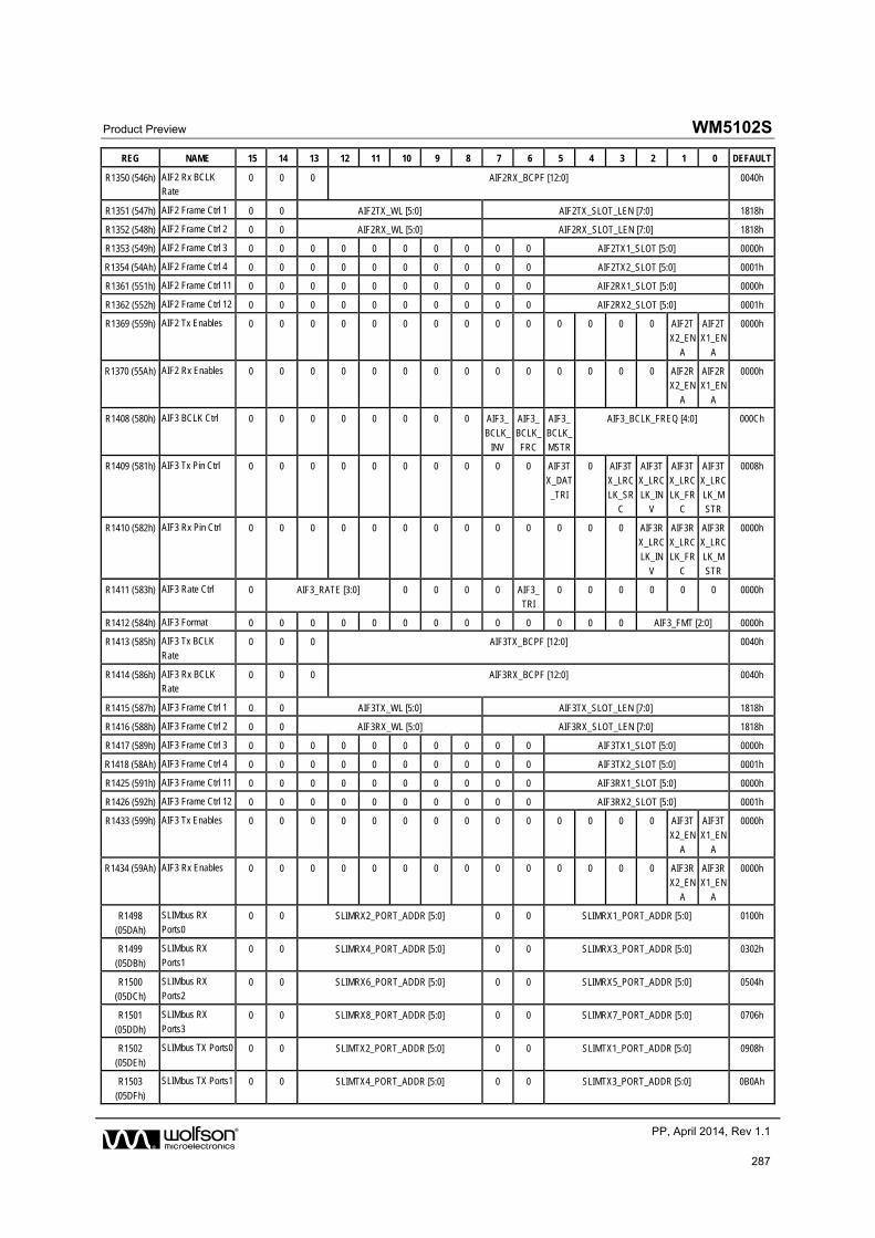
Product Preview WM5102S
w PP, April 2014, Rev 1.1
287
REG NAME 15 14 13 12 11 10 9 8 7 6 5 4 3 2 1 0 DEFAULT
R1350 (546h) AIF2 Rx BCLK Rate
0 0 0 AIF2RX_BCPF [12:0] 0040h
R1351 (547h) AIF2 Frame Ctrl 1 0 0 AIF2TX_WL [5:0] AIF2TX_SLOT_LEN [7:0] 1818h
R1352 (548h) AIF2 Frame Ctrl 2 0 0 AIF2RX_WL [5:0] AIF2RX_SLOT_LEN [7:0] 1818h
R1353 (549h) AIF2 Frame Ctrl 3 0 0 0 0 0 0 0 0 0 0 AIF2TX1_SLOT [5:0] 0000h
R1354 (54Ah) AIF2 Frame Ctrl 4 0 0 0 0 0 0 0 0 0 0 AIF2TX2_SLOT [5:0] 0001h
R1361 (551h) AIF2 Frame Ctrl 11 0 0 0 0 0 0 0 0 0 0 AIF2RX1_SLOT [5:0] 0000h
R1362 (552h) AIF2 Frame Ctrl 12 0 0 0 0 0 0 0 0 0 0 AIF2RX2_SLOT [5:0] 0001h
R1369 (559h) AIF2 Tx Enables 0 0 0 0 0 0 0 0 0 0 0 0 0 0 AIF2TX2_EN
A
AIF2TX1_EN
A
0000h
R1370 (55Ah) AIF2 Rx Enables 0 0 0 0 0 0 0 0 0 0 0 0 0 0 AIF2RX2_EN
A
AIF2RX1_EN
A
0000h
R1408 (580h) AIF3 BCLK Ctrl 0 0 0 0 0 0 0 0 AIF3_
BCLK_INV
AIF3_
BCLK_FRC
AIF3_
BCLK_MSTR
AIF3_BCLK_FREQ [4:0] 000Ch
R1409 (581h) AIF3 Tx Pin Ctrl 0 0 0 0 0 0 0 0 0 0 AIF3T
X_DAT_TRI
0 AIF3T
X_LRCLK_SR
C
AIF3T
X_LRCLK_IN
V
AIF3T
X_LRCLK_FR
C
AIF3T
X_LRCLK_MSTR
0008h
R1410 (582h) AIF3 Rx Pin Ctrl 0 0 0 0 0 0 0 0 0 0 0 0 0 AIF3R
X_LRCLK_IN
V
AIF3R
X_LRCLK_FR
C
AIF3R
X_LRCLK_M
STR
0000h
R1411 (583h) AIF3 Rate Ctrl 0 AIF3_RATE [3:0] 0 0 0 0 AIF3_TRI
0 0 0 0 0 0 0000h
R1412 (584h) AIF3 Format 0 0 0 0 0 0 0 0 0 0 0 0 0 AIF3_FMT [2:0] 0000h
R1413 (585h) AIF3 Tx BCLK
Rate 0 0 0 AIF3TX_BCPF [12:0] 0040h
R1414 (586h) AIF3 Rx BCLK Rate
0 0 0 AIF3RX_BCPF [12:0] 0040h
R1415 (587h) AIF3 Frame Ctrl 1 0 0 AIF3TX_WL [5:0] AIF3TX_SLOT_LEN [7:0] 1818h
R1416 (588h) AIF3 Frame Ctrl 2 0 0 AIF3RX_WL [5:0] AIF3RX_SLOT_LEN [7:0] 1818h
R1417 (589h) AIF3 Frame Ctrl 3 0 0 0 0 0 0 0 0 0 0 AIF3TX1_SLOT [5:0] 0000h
R1418 (58Ah) AIF3 Frame Ctrl 4 0 0 0 0 0 0 0 0 0 0 AIF3TX2_SLOT [5:0] 0001h
R1425 (591h) AIF3 Frame Ctrl 11 0 0 0 0 0 0 0 0 0 0 AIF3RX1_SLOT [5:0] 0000h
R1426 (592h) AIF3 Frame Ctrl 12 0 0 0 0 0 0 0 0 0 0 AIF3RX2_SLOT [5:0] 0001h
R1433 (599h) AIF3 Tx Enables 0 0 0 0 0 0 0 0 0 0 0 0 0 0 AIF3TX2_EN
A
AIF3TX1_EN
A
0000h
R1434 (59Ah) AIF3 Rx Enables 0 0 0 0 0 0 0 0 0 0 0 0 0 0 AIF3R
X2_ENA
AIF3R
X1_ENA
0000h
R1498
(05DAh)
SLIMbus RX
Ports0 0 0 SLIMRX2_PORT_ADDR [5:0] 0 0 SLIMRX1_PORT_ADDR [5:0] 0100h
R1499 (05DBh)
SLIMbus RX Ports1
0 0 SLIMRX4_PORT_ADDR [5:0] 0 0 SLIMRX3_PORT_ADDR [5:0] 0302h
R1500 (05DCh)
SLIMbus RX
Ports2 0 0 SLIMRX6_PORT_ADDR [5:0] 0 0 SLIMRX5_PORT_ADDR [5:0] 0504h
R1501
(05DDh)
SLIMbus RX
Ports3 0 0 SLIMRX8_PORT_ADDR [5:0] 0 0 SLIMRX7_PORT_ADDR [5:0] 0706h
R1502 (05DEh)
SLIMbus TX Ports0 0 0 SLIMTX2_PORT_ADDR [5:0] 0 0 SLIMTX1_PORT_ADDR [5:0] 0908h
R1503 (05DFh)
SLIMbus TX Ports1 0 0 SLIMTX4_PORT_ADDR [5:0] 0 0 SLIMTX3_PORT_ADDR [5:0] 0B0Ah
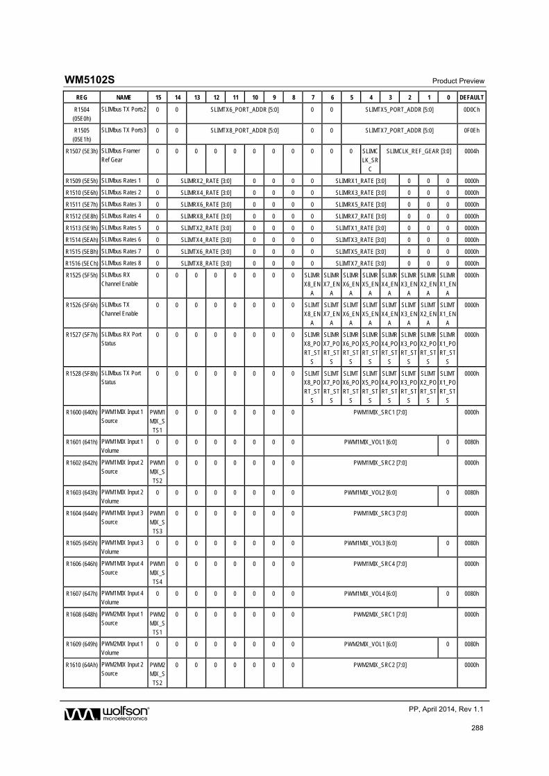
WM5102S Product Preview
w PP, April 2014, Rev 1.1
288
REG NAME 15 14 13 12 11 10 9 8 7 6 5 4 3 2 1 0 DEFAULT
R1504
(05E0h)
SLIMbus TX Ports2 0 0 SLIMTX6_PORT_ADDR [5:0] 0 0 SLIMTX5_PORT_ADDR [5:0] 0D0Ch
R1505 (05E1h)
SLIMbus TX Ports3 0 0 SLIMTX8_PORT_ADDR [5:0] 0 0 SLIMTX7_PORT_ADDR [5:0] 0F0Eh
R1507 (5E3h) SLIMbus Framer
Ref Gear 0 0 0 0 0 0 0 0 0 0 0 SLIMC
LK_SRC
SLIMCLK_REF_GEAR [3:0] 0004h
R1509 (5E5h) SLIMbus Rates 1 0 SLIMRX2_RATE [3:0] 0 0 0 0 SLIMRX1_RATE [3:0] 0 0 0 0000h
R1510 (5E6h) SLIMbus Rates 2 0 SLIMRX4_RATE [3:0] 0 0 0 0 SLIMRX3_RATE [3:0] 0 0 0 0000h
R1511 (5E7h) SLIMbus Rates 3 0 SLIMRX6_RATE [3:0] 0 0 0 0 SLIMRX5_RATE [3:0] 0 0 0 0000h
R1512 (5E8h) SLIMbus Rates 4 0 SLIMRX8_RATE [3:0] 0 0 0 0 SLIMRX7_RATE [3:0] 0 0 0 0000h
R1513 (5E9h) SLIMbus Rates 5 0 SLIMTX2_RATE [3:0] 0 0 0 0 SLIMTX1_RATE [3:0] 0 0 0 0000h
R1514 (5EAh) SLIMbus Rates 6 0 SLIMTX4_RATE [3:0] 0 0 0 0 SLIMTX3_RATE [3:0] 0 0 0 0000h
R1515 (5EBh) SLIMbus Rates 7 0 SLIMTX6_RATE [3:0] 0 0 0 0 SLIMTX5_RATE [3:0] 0 0 0 0000h
R1516 (5ECh) SLIMbus Rates 8 0 SLIMTX8_RATE [3:0] 0 0 0 0 SLIMTX7_RATE [3:0] 0 0 0 0000h
R1525 (5F5h) SLIMbus RX Channel Enable
0 0 0 0 0 0 0 0 SLIMRX8_EN
A
SLIMRX7_EN
A
SLIMRX6_EN
A
SLIMRX5_EN
A
SLIMRX4_EN
A
SLIMRX3_EN
A
SLIMRX2_EN
A
SLIMRX1_EN
A
0000h
R1526 (5F6h) SLIMbus TX Channel Enable
0 0 0 0 0 0 0 0 SLIMTX8_EN
A
SLIMTX7_EN
A
SLIMTX6_EN
A
SLIMTX5_EN
A
SLIMTX4_EN
A
SLIMTX3_EN
A
SLIMTX2_EN
A
SLIMTX1_EN
A
0000h
R1527 (5F7h) SLIMbus RX Port Status
0 0 0 0 0 0 0 0 SLIMR
X8_PORT_ST
S
SLIMR
X7_PORT_ST
S
SLIMR
X6_PORT_ST
S
SLIMR
X5_PORT_ST
S
SLIMR
X4_PORT_ST
S
SLIMR
X3_PORT_ST
S
SLIMR
X2_PORT_ST
S
SLIMR
X1_PORT_ST
S
0000h
R1528 (5F8h) SLIMbus TX Port Status
0 0 0 0 0 0 0 0 SLIMTX8_PORT_ST
S
SLIMTX7_PORT_ST
S
SLIMTX6_PORT_ST
S
SLIMTX5_PORT_ST
S
SLIMTX4_PORT_ST
S
SLIMTX3_PORT_ST
S
SLIMTX2_PORT_ST
S
SLIMTX1_PORT_ST
S
0000h
R1600 (640h) PWM1MIX Input 1 Source
PWM1MIX_S
TS1
0 0 0 0 0 0 0 PWM1MIX_SRC1 [7:0] 0000h
R1601 (641h) PWM1MIX Input 1 Volume
0 0 0 0 0 0 0 0 PWM1MIX_VOL1 [6:0] 0 0080h
R1602 (642h) PWM1MIX Input 2
Source PWM1MIX_S
TS2
0 0 0 0 0 0 0 PWM1MIX_SRC2 [7:0] 0000h
R1603 (643h) PWM1MIX Input 2 Volume
0 0 0 0 0 0 0 0 PWM1MIX_VOL2 [6:0] 0 0080h
R1604 (644h) PWM1MIX Input 3
Source PWM1
MIX_STS3
0 0 0 0 0 0 0 PWM1MIX_SRC3 [7:0] 0000h
R1605 (645h) PWM1MIX Input 3
Volume 0 0 0 0 0 0 0 0 PWM1MIX_VOL3 [6:0] 0 0080h
R1606 (646h) PWM1MIX Input 4 Source
PWM1
MIX_STS4
0 0 0 0 0 0 0 PWM1MIX_SRC4 [7:0] 0000h
R1607 (647h) PWM1MIX Input 4
Volume 0 0 0 0 0 0 0 0 PWM1MIX_VOL4 [6:0] 0 0080h
R1608 (648h) PWM2MIX Input 1 Source
PWM2MIX_S
TS1
0 0 0 0 0 0 0 PWM2MIX_SRC1 [7:0] 0000h
R1609 (649h) PWM2MIX Input 1 Volume
0 0 0 0 0 0 0 0 PWM2MIX_VOL1 [6:0] 0 0080h
R1610 (64Ah) PWM2MIX Input 2 Source
PWM2MIX_S
TS2
0 0 0 0 0 0 0 PWM2MIX_SRC2 [7:0] 0000h
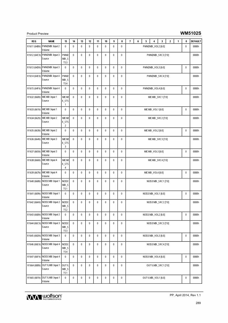
Product Preview WM5102S
w PP, April 2014, Rev 1.1
289
REG NAME 15 14 13 12 11 10 9 8 7 6 5 4 3 2 1 0 DEFAULT
R1611 (64Bh) PWM2MIX Input 2 Volume
0 0 0 0 0 0 0 0 PWM2MIX_VOL2 [6:0] 0 0080h
R1612 (64Ch) PWM2MIX Input 3
Source PWM2MIX_S
TS3
0 0 0 0 0 0 0 PWM2MIX_SRC3 [7:0] 0000h
R1613 (64Dh) PWM2MIX Input 3 Volume
0 0 0 0 0 0 0 0 PWM2MIX_VOL3 [6:0] 0 0080h
R1614 (64Eh) PWM2MIX Input 4
Source PWM2
MIX_STS4
0 0 0 0 0 0 0 PWM2MIX_SRC4 [7:0] 0000h
R1615 (64Fh) PWM2MIX Input 4 Volume
0 0 0 0 0 0 0 0 PWM2MIX_VOL4 [6:0] 0 0080h
R1632 (660h) MICMIX Input 1
Source MICMI
X_STS1
0 0 0 0 0 0 0 MICMIX_SRC1 [7:0] 0000h
R1633 (661h) MICMIX Input 1
Volume 0 0 0 0 0 0 0 0 MICMIX_VOL1 [6:0] 0 0080h
R1634 (662h) MICMIX Input 2 Source
MICMI
X_STS2
0 0 0 0 0 0 0 MICMIX_SRC2 [7:0] 0000h
R1635 (663h) MICMIX Input 2
Volume 0 0 0 0 0 0 0 0 MICMIX_VOL2 [6:0] 0 0080h
R1636 (664h) MICMIX Input 3 Source
MICMIX_STS
3
0 0 0 0 0 0 0 MICMIX_SRC3 [7:0] 0000h
R1637 (665h) MICMIX Input 3 Volume
0 0 0 0 0 0 0 0 MICMIX_VOL3 [6:0] 0 0080h
R1638 (666h) MICMIX Input 4 Source
MICMIX_STS
4
0 0 0 0 0 0 0 MICMIX_SRC4 [7:0] 0000h
R1639 (667h) MICMIX Input 4 Volume
0 0 0 0 0 0 0 0 MICMIX_VOL4 [6:0] 0 0080h
R1640 (668h) NOISEMIX Input 1
Source NOISEMIX_S
TS1
0 0 0 0 0 0 0 NOISEMIX_SRC1 [7:0] 0000h
R1641 (669h) NOISEMIX Input 1 Volume
0 0 0 0 0 0 0 0 NOISEMIX_VOL1 [6:0] 0 0080h
R1642 (66Ah) NOISEMIX Input 2
Source NOISE
MIX_STS2
0 0 0 0 0 0 0 NOISEMIX_SRC2 [7:0] 0000h
R1643 (66Bh) NOISEMIX Input 2
Volume 0 0 0 0 0 0 0 0 NOISEMIX_VOL2 [6:0] 0 0080h
R1644 (66Ch) NOISEMIX Input 3 Source
NOISE
MIX_STS3
0 0 0 0 0 0 0 NOISEMIX_SRC3 [7:0] 0000h
R1645 (66Dh) NOISEMIX Input 3
Volume 0 0 0 0 0 0 0 0 NOISEMIX_VOL3 [6:0] 0 0080h
R1646 (66Eh) NOISEMIX Input 4 Source
NOISEMIX_S
TS4
0 0 0 0 0 0 0 NOISEMIX_SRC4 [7:0] 0000h
R1647 (66Fh) NOISEMIX Input 4 Volume
0 0 0 0 0 0 0 0 NOISEMIX_VOL4 [6:0] 0 0080h
R1664 (680h) OUT1LMIX Input 1 Source
OUT1LMIX_S
TS1
0 0 0 0 0 0 0 OUT1LMIX_SRC1 [7:0] 0000h
R1665 (681h) OUT1LMIX Input 1 Volume
0 0 0 0 0 0 0 0 OUT1LMIX_VOL1 [6:0] 0 0080h

WM5102S Product Preview
w PP, April 2014, Rev 1.1
290
REG NAME 15 14 13 12 11 10 9 8 7 6 5 4 3 2 1 0 DEFAULT
R1666 (682h) OUT1LMIX Input 2 Source
OUT1L
MIX_STS2
0 0 0 0 0 0 0 OUT1LMIX_SRC2 [7:0] 0000h
R1667 (683h) OUT1LMIX Input 2
Volume 0 0 0 0 0 0 0 0 OUT1LMIX_VOL2 [6:0] 0 0080h
R1668 (684h) OUT1LMIX Input 3 Source
OUT1LMIX_S
TS3
0 0 0 0 0 0 0 OUT1LMIX_SRC3 [7:0] 0000h
R1669 (685h) OUT1LMIX Input 3 Volume
0 0 0 0 0 0 0 0 OUT1LMIX_VOL3 [6:0] 0 0080h
R1670 (686h) OUT1LMIX Input 4 Source
OUT1LMIX_S
TS4
0 0 0 0 0 0 0 OUT1LMIX_SRC4 [7:0] 0000h
R1671 (687h) OUT1LMIX Input 4 Volume
0 0 0 0 0 0 0 0 OUT1LMIX_VOL4 [6:0] 0 0080h
R1672 (688h) OUT1RMIX Input 1
Source OUT1RMIX_
STS1
0 0 0 0 0 0 0 OUT1RMIX_SRC1 [7:0] 0000h
R1673 (689h) OUT1RMIX Input 1 Volume
0 0 0 0 0 0 0 0 OUT1RMIX_VOL1 [6:0] 0 0080h
R1674 (68Ah) OUT1RMIX Input 2
Source OUT1
RMIX_STS2
0 0 0 0 0 0 0 OUT1RMIX_SRC2 [7:0] 0000h
R1675 (68Bh) OUT1RMIX Input 2
Volume 0 0 0 0 0 0 0 0 OUT1RMIX_VOL2 [6:0] 0 0080h
R1676 (68Ch) OUT1RMIX Input 3 Source
OUT1
RMIX_STS3
0 0 0 0 0 0 0 OUT1RMIX_SRC3 [7:0] 0000h
R1677 (68Dh) OUT1RMIX Input 3
Volume 0 0 0 0 0 0 0 0 OUT1RMIX_VOL3 [6:0] 0 0080h
R1678 (68Eh) OUT1RMIX Input 4 Source
OUT1RMIX_STS4
0 0 0 0 0 0 0 OUT1RMIX_SRC4 [7:0] 0000h
R1679 (68Fh) OUT1RMIX Input 4
Volume 0 0 0 0 0 0 0 0 OUT1RMIX_VOL4 [6:0] 0 0080h
R1680 (690h) OUT2LMIX Input 1 Source
OUT2LMIX_S
TS1
0 0 0 0 0 0 0 OUT2LMIX_SRC1 [7:0] 0000h
R1681 (691h) OUT2LMIX Input 1 Volume
0 0 0 0 0 0 0 0 OUT2LMIX_VOL1 [6:0] 0 0080h
R1682 (692h) OUT2LMIX Input 2 Source
OUT2LMIX_S
TS2
0 0 0 0 0 0 0 OUT2LMIX_SRC2 [7:0] 0000h
R1683 (693h) OUT2LMIX Input 2 Volume
0 0 0 0 0 0 0 0 OUT2LMIX_VOL2 [6:0] 0 0080h
R1684 (694h) OUT2LMIX Input 3
Source OUT2LMIX_S
TS3
0 0 0 0 0 0 0 OUT2LMIX_SRC3 [7:0] 0000h
R1685 (695h) OUT2LMIX Input 3 Volume
0 0 0 0 0 0 0 0 OUT2LMIX_VOL3 [6:0] 0 0080h
R1686 (696h) OUT2LMIX Input 4
Source OUT2L
MIX_STS4
0 0 0 0 0 0 0 OUT2LMIX_SRC4 [7:0] 0000h
R1687 (697h) OUT2LMIX Input 4
Volume 0 0 0 0 0 0 0 0 OUT2LMIX_VOL4 [6:0] 0 0080h
R1688 (698h) OUT2RMIX Input 1 Source
OUT2
RMIX_STS1
0 0 0 0 0 0 0 OUT2RMIX_SRC1 [7:0] 0000h
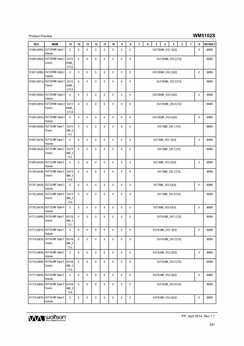
Product Preview WM5102S
w PP, April 2014, Rev 1.1
291
REG NAME 15 14 13 12 11 10 9 8 7 6 5 4 3 2 1 0 DEFAULT
R1689 (699h) OUT2RMIX Input 1 Volume
0 0 0 0 0 0 0 0 OUT2RMIX_VOL1 [6:0] 0 0080h
R1690 (69Ah) OUT2RMIX Input 2
Source OUT2RMIX_
STS2
0 0 0 0 0 0 0 OUT2RMIX_SRC2 [7:0] 0000h
R1691 (69Bh) OUT2RMIX Input 2 Volume
0 0 0 0 0 0 0 0 OUT2RMIX_VOL2 [6:0] 0 0080h
R1692 (69Ch) OUT2RMIX Input 3
Source OUT2
RMIX_STS3
0 0 0 0 0 0 0 OUT2RMIX_SRC3 [7:0] 0000h
R1693 (69Dh) OUT2RMIX Input 3 Volume
0 0 0 0 0 0 0 0 OUT2RMIX_VOL3 [6:0] 0 0080h
R1694 (69Eh) OUT2RMIX Input 4
Source OUT2
RMIX_STS4
0 0 0 0 0 0 0 OUT2RMIX_SRC4 [7:0] 0000h
R1695 (69Fh) OUT2RMIX Input 4
Volume 0 0 0 0 0 0 0 0 OUT2RMIX_VOL4 [6:0] 0 0080h
R1696 (6A0h) OUT3LMIX Input 1 Source
OUT3
MIX_STS1
0 0 0 0 0 0 0 OUT3MIX_SRC1 [7:0] 0000h
R1697 (6A1h) OUT3LMIX Input 1
Volume 0 0 0 0 0 0 0 0 OUT3MIX_VOL1 [6:0] 0 0080h
R1698 (6A2h) OUT3LMIX Input 2 Source
OUT3MIX_S
TS2
0 0 0 0 0 0 0 OUT3MIX_SRC2 [7:0] 0000h
R1699 (6A3h) OUT3LMIX Input 2 Volume
0 0 0 0 0 0 0 0 OUT3MIX_VOL2 [6:0] 0 0080h
R1700 (6A4h) OUT3LMIX Input 3 Source
OUT3MIX_S
TS3
0 0 0 0 0 0 0 OUT3MIX_SRC3 [7:0] 0000h
R1701 (6A5h) OUT3LMIX Input 3 Volume
0 0 0 0 0 0 0 0 OUT3MIX_VOL3 [6:0] 0 0080h
R1702 (6A6h) OUT3LMIX Input 4
Source OUT3MIX_S
TS4
0 0 0 0 0 0 0 OUT3MIX_SRC4 [7:0] 0000h
R1703 (6A7h) OUT3LMIX Input 4 Volume
0 0 0 0 0 0 0 0 OUT3MIX_VOL4 [6:0] 0 0080h
R1712 (6B0h) OUT4LMIX Input 1
Source OUT4L
MIX_STS1
0 0 0 0 0 0 0 OUT4LMIX_SRC1 [7:0] 0000h
R1713 (6B1h) OUT4LMIX Input 1
Volume 0 0 0 0 0 0 0 0 OUT4LMIX_VOL1 [6:0] 0 0080h
R1714 (6B2h) OUT4LMIX Input 2 Source
OUT4L
MIX_STS2
0 0 0 0 0 0 0 OUT4LMIX_SRC2 [7:0] 0000h
R1715 (6B3h) OUT4LMIX Input 2
Volume 0 0 0 0 0 0 0 0 OUT4LMIX_VOL2 [6:0] 0 0080h
R1716 (6B4h) OUT4LMIX Input 3 Source
OUT4LMIX_S
TS3
0 0 0 0 0 0 0 OUT4LMIX_SRC3 [7:0] 0000h
R1717 (6B5h) OUT4LMIX Input 3 Volume
0 0 0 0 0 0 0 0 OUT4LMIX_VOL3 [6:0] 0 0080h
R1718 (6B6h) OUT4LMIX Input 4 Source
OUT4LMIX_S
TS4
0 0 0 0 0 0 0 OUT4LMIX_SRC4 [7:0] 0000h
R1719 (6B7h) OUT4LMIX Input 4 Volume
0 0 0 0 0 0 0 0 OUT4LMIX_VOL4 [6:0] 0 0080h
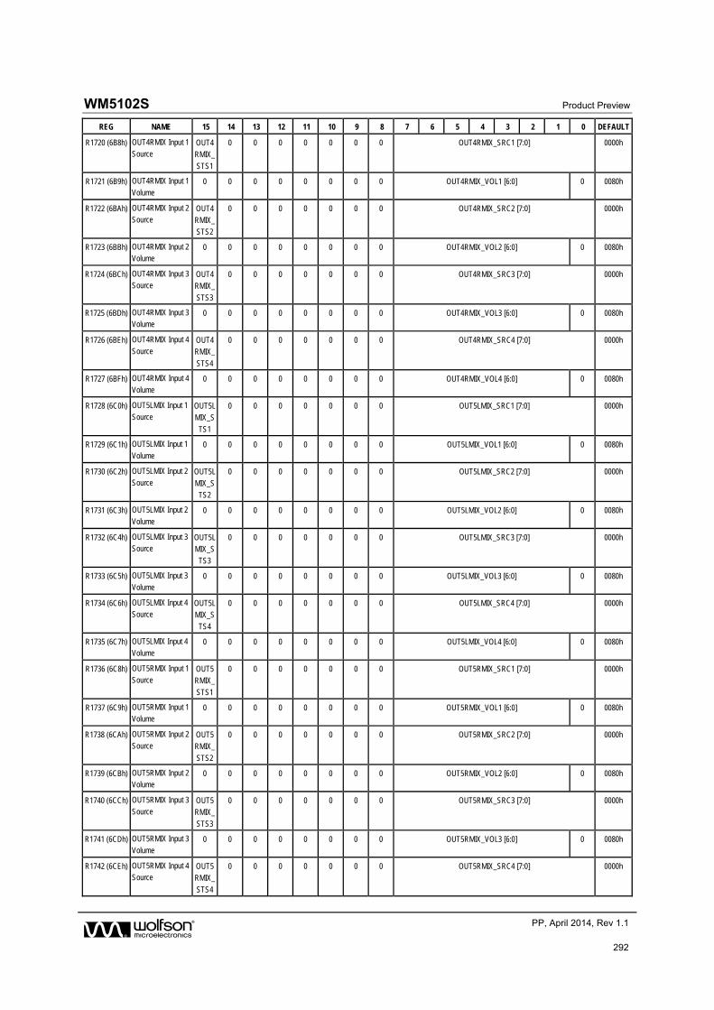
WM5102S Product Preview
w PP, April 2014, Rev 1.1
292
REG NAME 15 14 13 12 11 10 9 8 7 6 5 4 3 2 1 0 DEFAULT
R1720 (6B8h) OUT4RMIX Input 1 Source
OUT4
RMIX_STS1
0 0 0 0 0 0 0 OUT4RMIX_SRC1 [7:0] 0000h
R1721 (6B9h) OUT4RMIX Input 1
Volume 0 0 0 0 0 0 0 0 OUT4RMIX_VOL1 [6:0] 0 0080h
R1722 (6BAh) OUT4RMIX Input 2 Source
OUT4RMIX_STS2
0 0 0 0 0 0 0 OUT4RMIX_SRC2 [7:0] 0000h
R1723 (6BBh) OUT4RMIX Input 2 Volume
0 0 0 0 0 0 0 0 OUT4RMIX_VOL2 [6:0] 0 0080h
R1724 (6BCh) OUT4RMIX Input 3 Source
OUT4RMIX_
STS3
0 0 0 0 0 0 0 OUT4RMIX_SRC3 [7:0] 0000h
R1725 (6BDh) OUT4RMIX Input 3 Volume
0 0 0 0 0 0 0 0 OUT4RMIX_VOL3 [6:0] 0 0080h
R1726 (6BEh) OUT4RMIX Input 4
Source OUT4RMIX_
STS4
0 0 0 0 0 0 0 OUT4RMIX_SRC4 [7:0] 0000h
R1727 (6BFh) OUT4RMIX Input 4 Volume
0 0 0 0 0 0 0 0 OUT4RMIX_VOL4 [6:0] 0 0080h
R1728 (6C0h) OUT5LMIX Input 1
Source OUT5L
MIX_STS1
0 0 0 0 0 0 0 OUT5LMIX_SRC1 [7:0] 0000h
R1729 (6C1h) OUT5LMIX Input 1
Volume 0 0 0 0 0 0 0 0 OUT5LMIX_VOL1 [6:0] 0 0080h
R1730 (6C2h) OUT5LMIX Input 2 Source
OUT5L
MIX_STS2
0 0 0 0 0 0 0 OUT5LMIX_SRC2 [7:0] 0000h
R1731 (6C3h) OUT5LMIX Input 2
Volume 0 0 0 0 0 0 0 0 OUT5LMIX_VOL2 [6:0] 0 0080h
R1732 (6C4h) OUT5LMIX Input 3 Source
OUT5LMIX_S
TS3
0 0 0 0 0 0 0 OUT5LMIX_SRC3 [7:0] 0000h
R1733 (6C5h) OUT5LMIX Input 3
Volume 0 0 0 0 0 0 0 0 OUT5LMIX_VOL3 [6:0] 0 0080h
R1734 (6C6h) OUT5LMIX Input 4 Source
OUT5LMIX_S
TS4
0 0 0 0 0 0 0 OUT5LMIX_SRC4 [7:0] 0000h
R1735 (6C7h) OUT5LMIX Input 4 Volume
0 0 0 0 0 0 0 0 OUT5LMIX_VOL4 [6:0] 0 0080h
R1736 (6C8h) OUT5RMIX Input 1 Source
OUT5RMIX_
STS1
0 0 0 0 0 0 0 OUT5RMIX_SRC1 [7:0] 0000h
R1737 (6C9h) OUT5RMIX Input 1 Volume
0 0 0 0 0 0 0 0 OUT5RMIX_VOL1 [6:0] 0 0080h
R1738 (6CAh) OUT5RMIX Input 2
Source OUT5RMIX_
STS2
0 0 0 0 0 0 0 OUT5RMIX_SRC2 [7:0] 0000h
R1739 (6CBh) OUT5RMIX Input 2 Volume
0 0 0 0 0 0 0 0 OUT5RMIX_VOL2 [6:0] 0 0080h
R1740 (6CCh) OUT5RMIX Input 3
Source OUT5
RMIX_STS3
0 0 0 0 0 0 0 OUT5RMIX_SRC3 [7:0] 0000h
R1741 (6CDh) OUT5RMIX Input 3
Volume 0 0 0 0 0 0 0 0 OUT5RMIX_VOL3 [6:0] 0 0080h
R1742 (6CEh) OUT5RMIX Input 4 Source
OUT5
RMIX_STS4
0 0 0 0 0 0 0 OUT5RMIX_SRC4 [7:0] 0000h
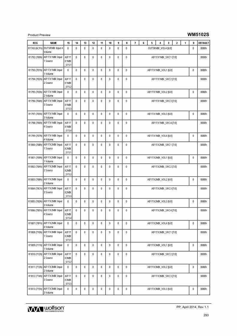
Product Preview WM5102S
w PP, April 2014, Rev 1.1
293
REG NAME 15 14 13 12 11 10 9 8 7 6 5 4 3 2 1 0 DEFAULT
R1743 (6CFh) OUT5RMIX Input 4 Volume
0 0 0 0 0 0 0 0 OUT5RMIX_VOL4 [6:0] 0 0080h
R1792 (700h) AIF1TX1MIX Input
1 Source AIF1TX1MIX
_STS1
0 0 0 0 0 0 0 AIF1TX1MIX_SRC1 [7:0] 0000h
R1793 (701h) AIF1TX1MIX Input 1 Volume
0 0 0 0 0 0 0 0 AIF1TX1MIX_VOL1 [6:0] 0 0080h
R1794 (702h) AIF1TX1MIX Input
2 Source AIF1T
X1MIX_STS2
0 0 0 0 0 0 0 AIF1TX1MIX_SRC2 [7:0] 0000h
R1795 (703h) AIF1TX1MIX Input 2 Volume
0 0 0 0 0 0 0 0 AIF1TX1MIX_VOL2 [6:0] 0 0080h
R1796 (704h) AIF1TX1MIX Input
3 Source AIF1T
X1MIX_STS3
0 0 0 0 0 0 0 AIF1TX1MIX_SRC3 [7:0] 0000h
R1797 (705h) AIF1TX1MIX Input
3 Volume 0 0 0 0 0 0 0 0 AIF1TX1MIX_VOL3 [6:0] 0 0080h
R1798 (706h) AIF1TX1MIX Input 4 Source
AIF1T
X1MIX_STS4
0 0 0 0 0 0 0 AIF1TX1MIX_SRC4 [7:0] 0000h
R1799 (707h) AIF1TX1MIX Input
4 Volume 0 0 0 0 0 0 0 0 AIF1TX1MIX_VOL4 [6:0] 0 0080h
R1800 (708h) AIF1TX2MIX Input 1 Source
AIF1TX2MIX_STS1
0 0 0 0 0 0 0 AIF1TX2MIX_SRC1 [7:0] 0000h
R1801 (709h) AIF1TX2MIX Input 1 Volume
0 0 0 0 0 0 0 0 AIF1TX2MIX_VOL1 [6:0] 0 0080h
R1802 (70Ah) AIF1TX2MIX Input 2 Source
AIF1TX2MIX
_STS2
0 0 0 0 0 0 0 AIF1TX2MIX_SRC2 [7:0] 0000h
R1803 (70Bh) AIF1TX2MIX Input 2 Volume
0 0 0 0 0 0 0 0 AIF1TX2MIX_VOL2 [6:0] 0 0080h
R1804 (70Ch) AIF1TX2MIX Input
3 Source AIF1TX2MIX
_STS3
0 0 0 0 0 0 0 AIF1TX2MIX_SRC3 [7:0] 0000h
R1805 (70Dh) AIF1TX2MIX Input 3 Volume
0 0 0 0 0 0 0 0 AIF1TX2MIX_VOL3 [6:0] 0 0080h
R1806 (70Eh) AIF1TX2MIX Input
4 Source AIF1T
X2MIX_STS4
0 0 0 0 0 0 0 AIF1TX2MIX_SRC4 [7:0] 0000h
R1807 (70Fh) AIF1TX2MIX Input
4 Volume 0 0 0 0 0 0 0 0 AIF1TX2MIX_VOL4 [6:0] 0 0080h
R1808 (710h) AIF1TX3MIX Input 1 Source
AIF1T
X3MIX_STS1
0 0 0 0 0 0 0 AIF1TX3MIX_SRC1 [7:0] 0000h
R1809 (711h) AIF1TX3MIX Input
1 Volume 0 0 0 0 0 0 0 0 AIF1TX3MIX_VOL1 [6:0] 0 0080h
R1810 (712h) AIF1TX3MIX Input 2 Source
AIF1TX3MIX_STS2
0 0 0 0 0 0 0 AIF1TX3MIX_SRC2 [7:0] 0000h
R1811 (713h) AIF1TX3MIX Input 2 Volume
0 0 0 0 0 0 0 0 AIF1TX3MIX_VOL2 [6:0] 0 0080h
R1812 (714h) AIF1TX3MIX Input 3 Source
AIF1TX3MIX
_STS3
0 0 0 0 0 0 0 AIF1TX3MIX_SRC3 [7:0] 0000h
R1813 (715h) AIF1TX3MIX Input 3 Volume
0 0 0 0 0 0 0 0 AIF1TX3MIX_VOL3 [6:0] 0 0080h
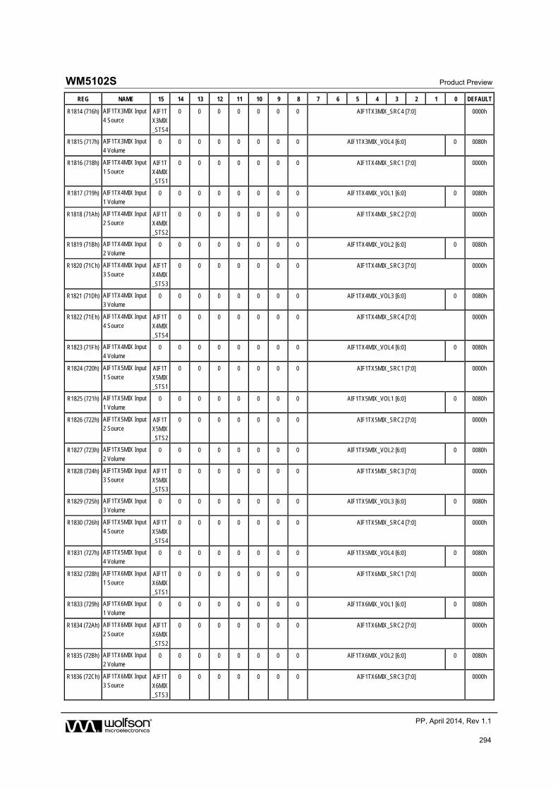
WM5102S Product Preview
w PP, April 2014, Rev 1.1
294
REG NAME 15 14 13 12 11 10 9 8 7 6 5 4 3 2 1 0 DEFAULT
R1814 (716h) AIF1TX3MIX Input 4 Source
AIF1T
X3MIX_STS4
0 0 0 0 0 0 0 AIF1TX3MIX_SRC4 [7:0] 0000h
R1815 (717h) AIF1TX3MIX Input
4 Volume 0 0 0 0 0 0 0 0 AIF1TX3MIX_VOL4 [6:0] 0 0080h
R1816 (718h) AIF1TX4MIX Input 1 Source
AIF1TX4MIX_STS1
0 0 0 0 0 0 0 AIF1TX4MIX_SRC1 [7:0] 0000h
R1817 (719h) AIF1TX4MIX Input 1 Volume
0 0 0 0 0 0 0 0 AIF1TX4MIX_VOL1 [6:0] 0 0080h
R1818 (71Ah) AIF1TX4MIX Input 2 Source
AIF1TX4MIX
_STS2
0 0 0 0 0 0 0 AIF1TX4MIX_SRC2 [7:0] 0000h
R1819 (71Bh) AIF1TX4MIX Input 2 Volume
0 0 0 0 0 0 0 0 AIF1TX4MIX_VOL2 [6:0] 0 0080h
R1820 (71Ch) AIF1TX4MIX Input
3 Source AIF1TX4MIX
_STS3
0 0 0 0 0 0 0 AIF1TX4MIX_SRC3 [7:0] 0000h
R1821 (71Dh) AIF1TX4MIX Input 3 Volume
0 0 0 0 0 0 0 0 AIF1TX4MIX_VOL3 [6:0] 0 0080h
R1822 (71Eh) AIF1TX4MIX Input
4 Source AIF1T
X4MIX_STS4
0 0 0 0 0 0 0 AIF1TX4MIX_SRC4 [7:0] 0000h
R1823 (71Fh) AIF1TX4MIX Input
4 Volume 0 0 0 0 0 0 0 0 AIF1TX4MIX_VOL4 [6:0] 0 0080h
R1824 (720h) AIF1TX5MIX Input 1 Source
AIF1T
X5MIX_STS1
0 0 0 0 0 0 0 AIF1TX5MIX_SRC1 [7:0] 0000h
R1825 (721h) AIF1TX5MIX Input
1 Volume 0 0 0 0 0 0 0 0 AIF1TX5MIX_VOL1 [6:0] 0 0080h
R1826 (722h) AIF1TX5MIX Input 2 Source
AIF1TX5MIX_STS2
0 0 0 0 0 0 0 AIF1TX5MIX_SRC2 [7:0] 0000h
R1827 (723h) AIF1TX5MIX Input
2 Volume 0 0 0 0 0 0 0 0 AIF1TX5MIX_VOL2 [6:0] 0 0080h
R1828 (724h) AIF1TX5MIX Input 3 Source
AIF1TX5MIX_STS3
0 0 0 0 0 0 0 AIF1TX5MIX_SRC3 [7:0] 0000h
R1829 (725h) AIF1TX5MIX Input 3 Volume
0 0 0 0 0 0 0 0 AIF1TX5MIX_VOL3 [6:0] 0 0080h
R1830 (726h) AIF1TX5MIX Input 4 Source
AIF1TX5MIX
_STS4
0 0 0 0 0 0 0 AIF1TX5MIX_SRC4 [7:0] 0000h
R1831 (727h) AIF1TX5MIX Input 4 Volume
0 0 0 0 0 0 0 0 AIF1TX5MIX_VOL4 [6:0] 0 0080h
R1832 (728h) AIF1TX6MIX Input
1 Source AIF1TX6MIX
_STS1
0 0 0 0 0 0 0 AIF1TX6MIX_SRC1 [7:0] 0000h
R1833 (729h) AIF1TX6MIX Input 1 Volume
0 0 0 0 0 0 0 0 AIF1TX6MIX_VOL1 [6:0] 0 0080h
R1834 (72Ah) AIF1TX6MIX Input
2 Source AIF1T
X6MIX_STS2
0 0 0 0 0 0 0 AIF1TX6MIX_SRC2 [7:0] 0000h
R1835 (72Bh) AIF1TX6MIX Input
2 Volume 0 0 0 0 0 0 0 0 AIF1TX6MIX_VOL2 [6:0] 0 0080h
R1836 (72Ch) AIF1TX6MIX Input 3 Source
AIF1T
X6MIX_STS3
0 0 0 0 0 0 0 AIF1TX6MIX_SRC3 [7:0] 0000h

Product Preview WM5102S
w PP, April 2014, Rev 1.1
295
REG NAME 15 14 13 12 11 10 9 8 7 6 5 4 3 2 1 0 DEFAULT
R1837 (72Dh) AIF1TX6MIX Input 3 Volume
0 0 0 0 0 0 0 0 AIF1TX6MIX_VOL3 [6:0] 0 0080h
R1838 (72Eh) AIF1TX6MIX Input
4 Source AIF1TX6MIX
_STS4
0 0 0 0 0 0 0 AIF1TX6MIX_SRC4 [7:0] 0000h
R1839 (72Fh) AIF1TX6MIX Input 4 Volume
0 0 0 0 0 0 0 0 AIF1TX6MIX_VOL4 [6:0] 0 0080h
R1840 (730h) AIF1TX7MIX Input
1 Source AIF1T
X7MIX_STS1
0 0 0 0 0 0 0 AIF1TX7MIX_SRC1 [7:0] 0000h
R1841 (731h) AIF1TX7MIX Input 1 Volume
0 0 0 0 0 0 0 0 AIF1TX7MIX_VOL1 [6:0] 0 0080h
R1842 (732h) AIF1TX7MIX Input
2 Source AIF1T
X7MIX_STS2
0 0 0 0 0 0 0 AIF1TX7MIX_SRC2 [7:0] 0000h
R1843 (733h) AIF1TX7MIX Input
2 Volume 0 0 0 0 0 0 0 0 AIF1TX7MIX_VOL2 [6:0] 0 0080h
R1844 (734h) AIF1TX7MIX Input 3 Source
AIF1T
X7MIX_STS3
0 0 0 0 0 0 0 AIF1TX7MIX_SRC3 [7:0] 0000h
R1845 (735h) AIF1TX7MIX Input
3 Volume 0 0 0 0 0 0 0 0 AIF1TX7MIX_VOL3 [6:0] 0 0080h
R1846 (736h) AIF1TX7MIX Input 4 Source
AIF1TX7MIX_STS4
0 0 0 0 0 0 0 AIF1TX7MIX_SRC4 [7:0] 0000h
R1847 (737h) AIF1TX7MIX Input 4 Volume
0 0 0 0 0 0 0 0 AIF1TX7MIX_VOL4 [6:0] 0 0080h
R1848 (738h) AIF1TX8MIX Input 1 Source
AIF1TX8MIX
_STS1
0 0 0 0 0 0 0 AIF1TX8MIX_SRC1 [7:0] 0000h
R1849 (739h) AIF1TX8MIX Input 1 Volume
0 0 0 0 0 0 0 0 AIF1TX8MIX_VOL1 [6:0] 0 0080h
R1850 (73Ah) AIF1TX8MIX Input
2 Source AIF1TX8MIX
_STS2
0 0 0 0 0 0 0 AIF1TX8MIX_SRC2 [7:0] 0000h
R1851 (73Bh) AIF1TX8MIX Input 2 Volume
0 0 0 0 0 0 0 0 AIF1TX8MIX_VOL2 [6:0] 0 0080h
R1852 (73Ch) AIF1TX8MIX Input
3 Source AIF1T
X8MIX_STS3
0 0 0 0 0 0 0 AIF1TX8MIX_SRC3 [7:0] 0000h
R1853 (73Dh) AIF1TX8MIX Input
3 Volume 0 0 0 0 0 0 0 0 AIF1TX8MIX_VOL3 [6:0] 0 0080h
R1854 (73Eh) AIF1TX8MIX Input 4 Source
AIF1T
X8MIX_STS4
0 0 0 0 0 0 0 AIF1TX8MIX_SRC4 [7:0] 0000h
R1855 (73Fh) AIF1TX8MIX Input
4 Volume 0 0 0 0 0 0 0 0 AIF1TX8MIX_VOL4 [6:0] 0 0080h
R1856 (740h) AIF2TX1MIX Input 1 Source
AIF2TX1MIX_STS1
0 0 0 0 0 0 0 AIF2TX1MIX_SRC1 [7:0] 0000h
R1857 (741h) AIF2TX1MIX Input 1 Volume
0 0 0 0 0 0 0 0 AIF2TX1MIX_VOL1 [6:0] 0 0080h
R1858 (742h) AIF2TX1MIX Input 2 Source
AIF2TX1MIX
_STS2
0 0 0 0 0 0 0 AIF2TX1MIX_SRC2 [7:0] 0000h
R1859 (743h) AIF2TX1MIX Input 2 Volume
0 0 0 0 0 0 0 0 AIF2TX1MIX_VOL2 [6:0] 0 0080h

WM5102S Product Preview
w PP, April 2014, Rev 1.1
296
REG NAME 15 14 13 12 11 10 9 8 7 6 5 4 3 2 1 0 DEFAULT
R1860 (744h) AIF2TX1MIX Input 3 Source
AIF2T
X1MIX_STS3
0 0 0 0 0 0 0 AIF2TX1MIX_SRC3 [7:0] 0000h
R1861 (745h) AIF2TX1MIX Input
3 Volume 0 0 0 0 0 0 0 0 AIF2TX1MIX_VOL3 [6:0] 0 0080h
R1862 (746h) AIF2TX1MIX Input 4 Source
AIF2TX1MIX_STS4
0 0 0 0 0 0 0 AIF2TX1MIX_SRC4 [7:0] 0000h
R1863 (747h) AIF2TX1MIX Input 4 Volume
0 0 0 0 0 0 0 0 AIF2TX1MIX_VOL4 [6:0] 0 0080h
R1864 (748h) AIF2TX2MIX Input 1 Source
AIF2TX2MIX
_STS1
0 0 0 0 0 0 0 AIF2TX2MIX_SRC1 [7:0] 0000h
R1865 (749h) AIF2TX2MIX Input 1 Volume
0 0 0 0 0 0 0 0 AIF2TX2MIX_VOL1 [6:0] 0 0080h
R1866 (74Ah) AIF2TX2MIX Input
2 Source AIF2TX2MIX
_STS2
0 0 0 0 0 0 0 AIF2TX2MIX_SRC2 [7:0] 0000h
R1867 (74Bh) AIF2TX2MIX Input 2 Volume
0 0 0 0 0 0 0 0 AIF2TX2MIX_VOL2 [6:0] 0 0080h
R1868 (74Ch) AIF2TX2MIX Input
3 Source AIF2T
X2MIX_STS3
0 0 0 0 0 0 0 AIF2TX2MIX_SRC3 [7:0] 0000h
R1869 (74Dh) AIF2TX2MIX Input
3 Volume 0 0 0 0 0 0 0 0 AIF2TX2MIX_VOL3 [6:0] 0 0080h
R1870 (74Eh) AIF2TX2MIX Input 4 Source
AIF2T
X2MIX_STS4
0 0 0 0 0 0 0 AIF2TX2MIX_SRC4 [7:0] 0000h
R1871 (74Fh) AIF2TX2MIX Input
4 Volume 0 0 0 0 0 0 0 0 AIF2TX2MIX_VOL4 [6:0] 0 0080h
R1920 (780h) AIF3TX1MIX Input 1 Source
AIF3TX1MIX_STS1
0 0 0 0 0 0 0 AIF3TX1MIX_SRC1 [7:0] 0000h
R1921 (781h) AIF3TX1MIX Input
1 Volume 0 0 0 0 0 0 0 0 AIF3TX1MIX_VOL1 [6:0] 0 0080h
R1922 (782h) AIF3TX1MIX Input 2 Source
AIF3TX1MIX_STS2
0 0 0 0 0 0 0 AIF3TX1MIX_SRC2 [7:0] 0000h
R1923 (783h) AIF3TX1MIX Input 2 Volume
0 0 0 0 0 0 0 0 AIF3TX1MIX_VOL2 [6:0] 0 0080h
R1924 (784h) AIF3TX1MIX Input 3 Source
AIF3TX1MIX
_STS3
0 0 0 0 0 0 0 AIF3TX1MIX_SRC3 [7:0] 0000h
R1925 (785h) AIF3TX1MIX Input 3 Volume
0 0 0 0 0 0 0 0 AIF3TX1MIX_VOL3 [6:0] 0 0080h
R1926 (786h) AIF3TX1MIX Input
4 Source AIF3TX1MIX
_STS4
0 0 0 0 0 0 0 AIF3TX1MIX_SRC4 [7:0] 0000h
R1927 (787h) AIF3TX1MIX Input 4 Volume
0 0 0 0 0 0 0 0 AIF3TX1MIX_VOL4 [6:0] 0 0080h
R1928 (788h) AIF3TX2MIX Input
1 Source AIF3T
X2MIX_STS1
0 0 0 0 0 0 0 AIF3TX2MIX_SRC1 [7:0] 0000h
R1929 (789h) AIF3TX2MIX Input
1 Volume 0 0 0 0 0 0 0 0 AIF3TX2MIX_VOL1 [6:0] 0 0080h
R1930 (78Ah) AIF3TX2MIX Input 2 Source
AIF3T
X2MIX_STS2
0 0 0 0 0 0 0 AIF3TX2MIX_SRC2 [7:0] 0000h
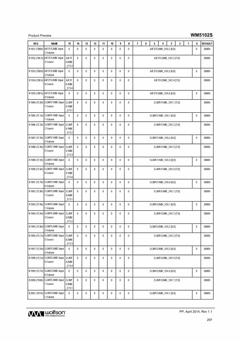
Product Preview WM5102S
w PP, April 2014, Rev 1.1
297
REG NAME 15 14 13 12 11 10 9 8 7 6 5 4 3 2 1 0 DEFAULT
R1931 (78Bh) AIF3TX2MIX Input 2 Volume
0 0 0 0 0 0 0 0 AIF3TX2MIX_VOL2 [6:0] 0 0080h
R1932 (78Ch) AIF3TX2MIX Input
3 Source AIF3TX2MIX
_STS3
0 0 0 0 0 0 0 AIF3TX2MIX_SRC3 [7:0] 0000h
R1933 (78Dh) AIF3TX2MIX Input 3 Volume
0 0 0 0 0 0 0 0 AIF3TX2MIX_VOL3 [6:0] 0 0080h
R1934 (78Eh) AIF3TX2MIX Input
4 Source AIF3T
X2MIX_STS4
0 0 0 0 0 0 0 AIF3TX2MIX_SRC4 [7:0] 0000h
R1935 (78Fh) AIF3TX2MIX Input 4 Volume
0 0 0 0 0 0 0 0 AIF3TX2MIX_VOL4 [6:0] 0 0080h
R1984 (7C0h) SLIMTX1MIX Input
1 Source SLIMT
X1MIX_STS1
0 0 0 0 0 0 0 SLIMTX1MIX_SRC1 [7:0] 0000h
R1985 (7C1h) SLIMTX1MIX Input
1 Volume 0 0 0 0 0 0 0 0 SLIMTX1MIX_VOL1 [6:0] 0 0080h
R1986 (7C2h) SLIMTX1MIX Input 2 Source
SLIMT
X1MIX_STS2
0 0 0 0 0 0 0 SLIMTX1MIX_SRC2 [7:0] 0000h
R1987 (7C3h) SLIMTX1MIX Input
2 Volume 0 0 0 0 0 0 0 0 SLIMTX1MIX_VOL2 [6:0] 0 0080h
R1988 (7C4h) SLIMTX1MIX Input 3 Source
SLIMTX1MIX_STS3
0 0 0 0 0 0 0 SLIMTX1MIX_SRC3 [7:0] 0000h
R1989 (7C5h) SLIMTX1MIX Input 3 Volume
0 0 0 0 0 0 0 0 SLIMTX1MIX_VOL3 [6:0] 0 0080h
R1990 (7C6h) SLIMTX1MIX Input 4 Source
SLIMTX1MIX
_STS4
0 0 0 0 0 0 0 SLIMTX1MIX_SRC4 [7:0] 0000h
R1991 (7C7h) SLIMTX1MIX Input 4 Volume
0 0 0 0 0 0 0 0 SLIMTX1MIX_VOL4 [6:0] 0 0080h
R1992 (7C8h) SLIMTX2MIX Input
1 Source SLIMTX2MIX
_STS1
0 0 0 0 0 0 0 SLIMTX2MIX_SRC1 [7:0] 0000h
R1993 (7C9h) SLIMTX2MIX Input 1 Volume
0 0 0 0 0 0 0 0 SLIMTX2MIX_VOL1 [6:0] 0 0080h
R1994 (7CAh) SLIMTX2MIX Input
2 Source SLIMT
X2MIX_STS2
0 0 0 0 0 0 0 SLIMTX2MIX_SRC2 [7:0] 0000h
R1995 (7CBh) SLIMTX2MIX Input
2 Volume 0 0 0 0 0 0 0 0 SLIMTX2MIX_VOL2 [6:0] 0 0080h
R1996 (7CCh) SLIMTX2MIX Input 3 Source
SLIMT
X2MIX_STS3
0 0 0 0 0 0 0 SLIMTX2MIX_SRC3 [7:0] 0000h
R1997 (7CDh) SLIMTX2MIX Input
3 Volume 0 0 0 0 0 0 0 0 SLIMTX2MIX_VOL3 [6:0] 0 0080h
R1998 (7CEh) SLIMTX2MIX Input 4 Source
SLIMTX2MIX_STS4
0 0 0 0 0 0 0 SLIMTX2MIX_SRC4 [7:0] 0000h
R1999 (7CFh) SLIMTX2MIX Input 4 Volume
0 0 0 0 0 0 0 0 SLIMTX2MIX_VOL4 [6:0] 0 0080h
R2000 (7D0h) SLIMTX3MIX Input 1 Source
SLIMTX3MIX
_STS1
0 0 0 0 0 0 0 SLIMTX3MIX_SRC1 [7:0] 0000h
R2001 (7D1h) SLIMTX3MIX Input 1 Volume
0 0 0 0 0 0 0 0 SLIMTX3MIX_VOL1 [6:0] 0 0080h

WM5102S Product Preview
w PP, April 2014, Rev 1.1
298
REG NAME 15 14 13 12 11 10 9 8 7 6 5 4 3 2 1 0 DEFAULT
R2002 (7D2h) SLIMTX3MIX Input 2 Source
SLIMT
X3MIX_STS2
0 0 0 0 0 0 0 SLIMTX3MIX_SRC2 [7:0] 0000h
R2003 (7D3h) SLIMTX3MIX Input
2 Volume 0 0 0 0 0 0 0 0 SLIMTX3MIX_VOL2 [6:0] 0 0080h
R2004 (7D4h) SLIMTX3MIX Input 3 Source
SLIMTX3MIX_STS3
0 0 0 0 0 0 0 SLIMTX3MIX_SRC3 [7:0] 0000h
R2005 (7D5h) SLIMTX3MIX Input 3 Volume
0 0 0 0 0 0 0 0 SLIMTX3MIX_VOL3 [6:0] 0 0080h
R2006 (7D6h) SLIMTX3MIX Input 4 Source
SLIMTX3MIX
_STS4
0 0 0 0 0 0 0 SLIMTX3MIX_SRC4 [7:0] 0000h
R2007 (7D7h) SLIMTX3MIX Input 4 Volume
0 0 0 0 0 0 0 0 SLIMTX3MIX_VOL4 [6:0] 0 0080h
R2008 (7D8h) SLIMTX4MIX Input
1 Source SLIMTX4MIX
_STS1
0 0 0 0 0 0 0 SLIMTX4MIX_SRC1 [7:0] 0000h
R2009 (7D9h) SLIMTX4MIX Input 1 Volume
0 0 0 0 0 0 0 0 SLIMTX4MIX_VOL1 [6:0] 0 0080h
R2010 (7DAh) SLIMTX4MIX Input
2 Source SLIMT
X4MIX_STS2
0 0 0 0 0 0 0 SLIMTX4MIX_SRC2 [7:0] 0000h
R2011 (7DBh) SLIMTX4MIX Input
2 Volume 0 0 0 0 0 0 0 0 SLIMTX4MIX_VOL2 [6:0] 0 0080h
R2012 (7DCh) SLIMTX4MIX Input 3 Source
SLIMT
X4MIX_STS3
0 0 0 0 0 0 0 SLIMTX4MIX_SRC3 [7:0] 0000h
R2013 (7DDh) SLIMTX4MIX Input
3 Volume 0 0 0 0 0 0 0 0 SLIMTX4MIX_VOL3 [6:0] 0 0080h
R2014 (7DEh) SLIMTX4MIX Input 4 Source
SLIMTX4MIX_STS4
0 0 0 0 0 0 0 SLIMTX4MIX_SRC4 [7:0] 0000h
R2015 (7DFh) SLIMTX4MIX Input
4 Volume 0 0 0 0 0 0 0 0 SLIMTX4MIX_VOL4 [6:0] 0 0080h
R2016 (7E0h) SLIMTX5MIX Input 1 Source
SLIMTX5MIX_STS1
0 0 0 0 0 0 0 SLIMTX5MIX_SRC1 [7:0] 0000h
R2017 (7E1h) SLIMTX5MIX Input 1 Volume
0 0 0 0 0 0 0 0 SLIMTX5MIX_VOL1 [6:0] 0 0080h
R2018 (7E2h) SLIMTX5MIX Input 2 Source
SLIMTX5MIX
_STS2
0 0 0 0 0 0 0 SLIMTX5MIX_SRC2 [7:0] 0000h
R2019 (7E3h) SLIMTX5MIX Input 2 Volume
0 0 0 0 0 0 0 0 SLIMTX5MIX_VOL2 [6:0] 0 0080h
R2020 (7E4h) SLIMTX5MIX Input
3 Source SLIMTX5MIX
_STS3
0 0 0 0 0 0 0 SLIMTX5MIX_SRC3 [7:0] 0000h
R2021 (7E5h) SLIMTX5MIX Input 3 Volume
0 0 0 0 0 0 0 0 SLIMTX5MIX_VOL3 [6:0] 0 0080h
R2022 (7E6h) SLIMTX5MIX Input
4 Source SLIMT
X5MIX_STS4
0 0 0 0 0 0 0 SLIMTX5MIX_SRC4 [7:0] 0000h
R2023 (7E7h) SLIMTX5MIX Input
4 Volume 0 0 0 0 0 0 0 0 SLIMTX5MIX_VOL4 [6:0] 0 0080h
R2024 (7E8h) SLIMTX6MIX Input 1 Source
SLIMT
X6MIX_STS1
0 0 0 0 0 0 0 SLIMTX6MIX_SRC1 [7:0] 0000h

Product Preview WM5102S
w PP, April 2014, Rev 1.1
299
REG NAME 15 14 13 12 11 10 9 8 7 6 5 4 3 2 1 0 DEFAULT
R2025 (7E9h) SLIMTX6MIX Input 1 Volume
0 0 0 0 0 0 0 0 SLIMTX6MIX_VOL1 [6:0] 0 0080h
R2026 (7EAh) SLIMTX6MIX Input
2 Source SLIMTX6MIX
_STS2
0 0 0 0 0 0 0 SLIMTX6MIX_SRC2 [7:0] 0000h
R2027 (7EBh) SLIMTX6MIX Input 2 Volume
0 0 0 0 0 0 0 0 SLIMTX6MIX_VOL2 [6:0] 0 0080h
R2028 (7ECh) SLIMTX6MIX Input
3 Source SLIMT
X6MIX_STS3
0 0 0 0 0 0 0 SLIMTX6MIX_SRC3 [7:0] 0000h
R2029 (7EDh) SLIMTX6MIX Input 3 Volume
0 0 0 0 0 0 0 0 SLIMTX6MIX_VOL3 [6:0] 0 0080h
R2030 (7EEh) SLIMTX6MIX Input
4 Source SLIMT
X6MIX_STS4
0 0 0 0 0 0 0 SLIMTX6MIX_SRC4 [7:0] 0000h
R2031 (7EFh) SLIMTX6MIX Input
4 Volume 0 0 0 0 0 0 0 0 SLIMTX6MIX_VOL4 [6:0] 0 0080h
R2032 (7F0h) SLIMTX7MIX Input 1 Source
SLIMT
X7MIX_STS1
0 0 0 0 0 0 0 SLIMTX7MIX_SRC1 [7:0] 0000h
R2033 (7F1h) SLIMTX7MIX Input
1 Volume 0 0 0 0 0 0 0 0 SLIMTX7MIX_VOL1 [6:0] 0 0080h
R2034 (7F2h) SLIMTX7MIX Input 2 Source
SLIMTX7MIX_STS2
0 0 0 0 0 0 0 SLIMTX7MIX_SRC2 [7:0] 0000h
R2035 (7F3h) SLIMTX7MIX Input 2 Volume
0 0 0 0 0 0 0 0 SLIMTX7MIX_VOL2 [6:0] 0 0080h
R2036 (7F4h) SLIMTX7MIX Input 3 Source
SLIMTX7MIX
_STS3
0 0 0 0 0 0 0 SLIMTX7MIX_SRC3 [7:0] 0000h
R2037 (7F5h) SLIMTX7MIX Input 3 Volume
0 0 0 0 0 0 0 0 SLIMTX7MIX_VOL3 [6:0] 0 0080h
R2038 (7F6h) SLIMTX7MIX Input
4 Source SLIMTX7MIX
_STS4
0 0 0 0 0 0 0 SLIMTX7MIX_SRC4 [7:0] 0000h
R2039 (7F7h) SLIMTX7MIX Input 4 Volume
0 0 0 0 0 0 0 0 SLIMTX7MIX_VOL4 [6:0] 0 0080h
R2040 (7F8h) SLIMTX8MIX Input
1 Source SLIMT
X8MIX_STS1
0 0 0 0 0 0 0 SLIMTX8MIX_SRC1 [7:0] 0000h
R2041 (7F9h) SLIMTX8MIX Input
1 Volume 0 0 0 0 0 0 0 0 SLIMTX8MIX_VOL1 [6:0] 0 0080h
R2042 (7FAh) SLIMTX8MIX Input 2 Source
SLIMT
X8MIX_STS2
0 0 0 0 0 0 0 SLIMTX8MIX_SRC2 [7:0] 0000h
R2043 (7FBh) SLIMTX8MIX Input
2 Volume 0 0 0 0 0 0 0 0 SLIMTX8MIX_VOL2 [6:0] 0 0080h
R2044 (7FCh) SLIMTX8MIX Input 3 Source
SLIMTX8MIX_STS3
0 0 0 0 0 0 0 SLIMTX8MIX_SRC3 [7:0] 0000h
R2045 (7FDh) SLIMTX8MIX Input 3 Volume
0 0 0 0 0 0 0 0 SLIMTX8MIX_VOL3 [6:0] 0 0080h
R2046 (7FEh) SLIMTX8MIX Input 4 Source
SLIMTX8MIX
_STS4
0 0 0 0 0 0 0 SLIMTX8MIX_SRC4 [7:0] 0000h
R2047 (7FFh) SLIMTX8MIX Input 4 Volume
0 0 0 0 0 0 0 0 SLIMTX8MIX_VOL4 [6:0] 0 0080h
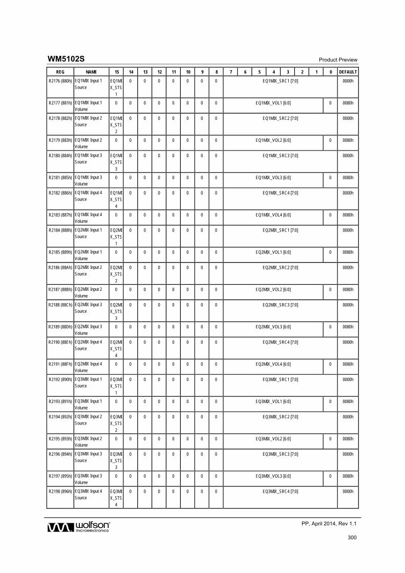
WM5102S Product Preview
w PP, April 2014, Rev 1.1
300
REG NAME 15 14 13 12 11 10 9 8 7 6 5 4 3 2 1 0 DEFAULT
R2176 (880h) EQ1MIX Input 1 Source
EQ1MI
X_STS1
0 0 0 0 0 0 0 EQ1MIX_SRC1 [7:0] 0000h
R2177 (881h) EQ1MIX Input 1
Volume 0 0 0 0 0 0 0 0 EQ1MIX_VOL1 [6:0] 0 0080h
R2178 (882h) EQ1MIX Input 2 Source
EQ1MIX_STS
2
0 0 0 0 0 0 0 EQ1MIX_SRC2 [7:0] 0000h
R2179 (883h) EQ1MIX Input 2 Volume
0 0 0 0 0 0 0 0 EQ1MIX_VOL2 [6:0] 0 0080h
R2180 (884h) EQ1MIX Input 3 Source
EQ1MIX_STS
3
0 0 0 0 0 0 0 EQ1MIX_SRC3 [7:0] 0000h
R2181 (885h) EQ1MIX Input 3 Volume
0 0 0 0 0 0 0 0 EQ1MIX_VOL3 [6:0] 0 0080h
R2182 (886h) EQ1MIX Input 4
Source EQ1MIX_STS
4
0 0 0 0 0 0 0 EQ1MIX_SRC4 [7:0] 0000h
R2183 (887h) EQ1MIX Input 4 Volume
0 0 0 0 0 0 0 0 EQ1MIX_VOL4 [6:0] 0 0080h
R2184 (888h) EQ2MIX Input 1
Source EQ2MI
X_STS1
0 0 0 0 0 0 0 EQ2MIX_SRC1 [7:0] 0000h
R2185 (889h) EQ2MIX Input 1
Volume 0 0 0 0 0 0 0 0 EQ2MIX_VOL1 [6:0] 0 0080h
R2186 (88Ah) EQ2MIX Input 2 Source
EQ2MI
X_STS2
0 0 0 0 0 0 0 EQ2MIX_SRC2 [7:0] 0000h
R2187 (88Bh) EQ2MIX Input 2
Volume 0 0 0 0 0 0 0 0 EQ2MIX_VOL2 [6:0] 0 0080h
R2188 (88Ch) EQ2MIX Input 3 Source
EQ2MIX_STS
3
0 0 0 0 0 0 0 EQ2MIX_SRC3 [7:0] 0000h
R2189 (88Dh) EQ2MIX Input 3
Volume 0 0 0 0 0 0 0 0 EQ2MIX_VOL3 [6:0] 0 0080h
R2190 (88Eh) EQ2MIX Input 4 Source
EQ2MIX_STS
4
0 0 0 0 0 0 0 EQ2MIX_SRC4 [7:0] 0000h
R2191 (88Fh) EQ2MIX Input 4 Volume
0 0 0 0 0 0 0 0 EQ2MIX_VOL4 [6:0] 0 0080h
R2192 (890h) EQ3MIX Input 1 Source
EQ3MIX_STS
1
0 0 0 0 0 0 0 EQ3MIX_SRC1 [7:0] 0000h
R2193 (891h) EQ3MIX Input 1 Volume
0 0 0 0 0 0 0 0 EQ3MIX_VOL1 [6:0] 0 0080h
R2194 (892h) EQ3MIX Input 2
Source EQ3MIX_STS
2
0 0 0 0 0 0 0 EQ3MIX_SRC2 [7:0] 0000h
R2195 (893h) EQ3MIX Input 2 Volume
0 0 0 0 0 0 0 0 EQ3MIX_VOL2 [6:0] 0 0080h
R2196 (894h) EQ3MIX Input 3
Source EQ3MI
X_STS3
0 0 0 0 0 0 0 EQ3MIX_SRC3 [7:0] 0000h
R2197 (895h) EQ3MIX Input 3
Volume 0 0 0 0 0 0 0 0 EQ3MIX_VOL3 [6:0] 0 0080h
R2198 (896h) EQ3MIX Input 4 Source
EQ3MI
X_STS4
0 0 0 0 0 0 0 EQ3MIX_SRC4 [7:0] 0000h
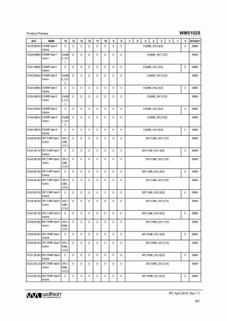
Product Preview WM5102S
w PP, April 2014, Rev 1.1
301
REG NAME 15 14 13 12 11 10 9 8 7 6 5 4 3 2 1 0 DEFAULT
R2199 (897h) EQ3MIX Input 4 Volume
0 0 0 0 0 0 0 0 EQ3MIX_VOL4 [6:0] 0 0080h
R2200 (898h) EQ4MIX Input 1
Source EQ4MIX_STS
1
0 0 0 0 0 0 0 EQ4MIX_SRC1 [7:0] 0000h
R2201 (899h) EQ4MIX Input 1 Volume
0 0 0 0 0 0 0 0 EQ4MIX_VOL1 [6:0] 0 0080h
R2202 (89Ah) EQ4MIX Input 2
Source EQ4MI
X_STS2
0 0 0 0 0 0 0 EQ4MIX_SRC2 [7:0] 0000h
R2203 (89Bh) EQ4MIX Input 2 Volume
0 0 0 0 0 0 0 0 EQ4MIX_VOL2 [6:0] 0 0080h
R2204 (89Ch) EQ4MIX Input 3
Source EQ4MI
X_STS3
0 0 0 0 0 0 0 EQ4MIX_SRC3 [7:0] 0000h
R2205 (89Dh) EQ4MIX Input 3
Volume 0 0 0 0 0 0 0 0 EQ4MIX_VOL3 [6:0] 0 0080h
R2206 (89Eh) EQ4MIX Input 4 Source
EQ4MI
X_STS4
0 0 0 0 0 0 0 EQ4MIX_SRC4 [7:0] 0000h
R2207 (89Fh) EQ4MIX Input 4
Volume 0 0 0 0 0 0 0 0 EQ4MIX_VOL4 [6:0] 0 0080h
R2240 (8C0h) DRC1LMIX Input 1 Source
DRC1LMIX_STS1
0 0 0 0 0 0 0 DRC1LMIX_SRC1 [7:0] 0000h
R2241 (8C1h) DRC1LMIX Input 1 Volume
0 0 0 0 0 0 0 0 DRC1LMIX_VOL1 [6:0] 0 0080h
R2242 (8C2h) DRC1LMIX Input 2 Source
DRC1LMIX_
STS2
0 0 0 0 0 0 0 DRC1LMIX_SRC2 [7:0] 0000h
R2243 (8C3h) DRC1LMIX Input 2 Volume
0 0 0 0 0 0 0 0 DRC1LMIX_VOL2 [6:0] 0 0080h
R2244 (8C4h) DRC1LMIX Input 3
Source DRC1LMIX_
STS3
0 0 0 0 0 0 0 DRC1LMIX_SRC3 [7:0] 0000h
R2245 (8C5h) DRC1LMIX Input 3 Volume
0 0 0 0 0 0 0 0 DRC1LMIX_VOL3 [6:0] 0 0080h
R2246 (8C6h) DRC1LMIX Input 4
Source DRC1
LMIX_STS4
0 0 0 0 0 0 0 DRC1LMIX_SRC4 [7:0] 0000h
R2247 (8C7h) DRC1LMIX Input 4
Volume 0 0 0 0 0 0 0 0 DRC1LMIX_VOL4 [6:0] 0 0080h
R2248 (8C8h) DRC1RMIX Input 1 Source
DRC1
RMIX_STS1
0 0 0 0 0 0 0 DRC1RMIX_SRC1 [7:0] 0000h
R2249 (8C9h) DRC1RMIX Input 1
Volume 0 0 0 0 0 0 0 0 DRC1RMIX_VOL1 [6:0] 0 0080h
R2250 (8CAh) DRC1RMIX Input 2 Source
DRC1RMIX_STS2
0 0 0 0 0 0 0 DRC1RMIX_SRC2 [7:0] 0000h
R2251 (8CBh) DRC1RMIX Input 2 Volume
0 0 0 0 0 0 0 0 DRC1RMIX_VOL2 [6:0] 0 0080h
R2252 (8CCh) DRC1RMIX Input 3 Source
DRC1RMIX_
STS3
0 0 0 0 0 0 0 DRC1RMIX_SRC3 [7:0] 0000h
R2253 (8CDh) DRC1RMIX Input 3 Volume
0 0 0 0 0 0 0 0 DRC1RMIX_VOL3 [6:0] 0 0080h
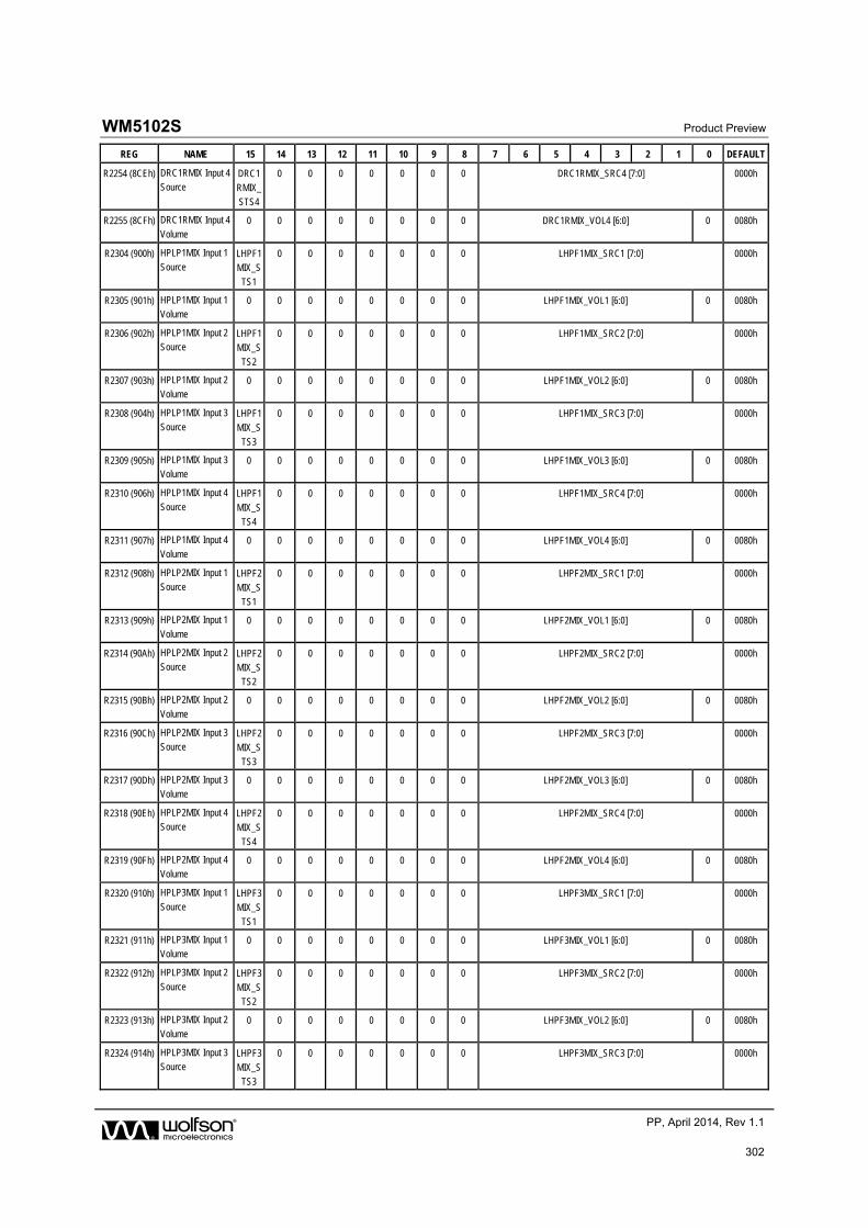
WM5102S Product Preview
w PP, April 2014, Rev 1.1
302
REG NAME 15 14 13 12 11 10 9 8 7 6 5 4 3 2 1 0 DEFAULT
R2254 (8CEh) DRC1RMIX Input 4 Source
DRC1
RMIX_STS4
0 0 0 0 0 0 0 DRC1RMIX_SRC4 [7:0] 0000h
R2255 (8CFh) DRC1RMIX Input 4
Volume 0 0 0 0 0 0 0 0 DRC1RMIX_VOL4 [6:0] 0 0080h
R2304 (900h) HPLP1MIX Input 1 Source
LHPF1MIX_S
TS1
0 0 0 0 0 0 0 LHPF1MIX_SRC1 [7:0] 0000h
R2305 (901h) HPLP1MIX Input 1 Volume
0 0 0 0 0 0 0 0 LHPF1MIX_VOL1 [6:0] 0 0080h
R2306 (902h) HPLP1MIX Input 2 Source
LHPF1MIX_S
TS2
0 0 0 0 0 0 0 LHPF1MIX_SRC2 [7:0] 0000h
R2307 (903h) HPLP1MIX Input 2 Volume
0 0 0 0 0 0 0 0 LHPF1MIX_VOL2 [6:0] 0 0080h
R2308 (904h) HPLP1MIX Input 3
Source LHPF1MIX_S
TS3
0 0 0 0 0 0 0 LHPF1MIX_SRC3 [7:0] 0000h
R2309 (905h) HPLP1MIX Input 3 Volume
0 0 0 0 0 0 0 0 LHPF1MIX_VOL3 [6:0] 0 0080h
R2310 (906h) HPLP1MIX Input 4
Source LHPF1
MIX_STS4
0 0 0 0 0 0 0 LHPF1MIX_SRC4 [7:0] 0000h
R2311 (907h) HPLP1MIX Input 4
Volume 0 0 0 0 0 0 0 0 LHPF1MIX_VOL4 [6:0] 0 0080h
R2312 (908h) HPLP2MIX Input 1 Source
LHPF2
MIX_STS1
0 0 0 0 0 0 0 LHPF2MIX_SRC1 [7:0] 0000h
R2313 (909h) HPLP2MIX Input 1
Volume 0 0 0 0 0 0 0 0 LHPF2MIX_VOL1 [6:0] 0 0080h
R2314 (90Ah) HPLP2MIX Input 2 Source
LHPF2MIX_S
TS2
0 0 0 0 0 0 0 LHPF2MIX_SRC2 [7:0] 0000h
R2315 (90Bh) HPLP2MIX Input 2
Volume 0 0 0 0 0 0 0 0 LHPF2MIX_VOL2 [6:0] 0 0080h
R2316 (90Ch) HPLP2MIX Input 3 Source
LHPF2MIX_S
TS3
0 0 0 0 0 0 0 LHPF2MIX_SRC3 [7:0] 0000h
R2317 (90Dh) HPLP2MIX Input 3 Volume
0 0 0 0 0 0 0 0 LHPF2MIX_VOL3 [6:0] 0 0080h
R2318 (90Eh) HPLP2MIX Input 4 Source
LHPF2MIX_S
TS4
0 0 0 0 0 0 0 LHPF2MIX_SRC4 [7:0] 0000h
R2319 (90Fh) HPLP2MIX Input 4 Volume
0 0 0 0 0 0 0 0 LHPF2MIX_VOL4 [6:0] 0 0080h
R2320 (910h) HPLP3MIX Input 1
Source LHPF3MIX_S
TS1
0 0 0 0 0 0 0 LHPF3MIX_SRC1 [7:0] 0000h
R2321 (911h) HPLP3MIX Input 1 Volume
0 0 0 0 0 0 0 0 LHPF3MIX_VOL1 [6:0] 0 0080h
R2322 (912h) HPLP3MIX Input 2
Source LHPF3
MIX_STS2
0 0 0 0 0 0 0 LHPF3MIX_SRC2 [7:0] 0000h
R2323 (913h) HPLP3MIX Input 2
Volume 0 0 0 0 0 0 0 0 LHPF3MIX_VOL2 [6:0] 0 0080h
R2324 (914h) HPLP3MIX Input 3 Source
LHPF3
MIX_STS3
0 0 0 0 0 0 0 LHPF3MIX_SRC3 [7:0] 0000h
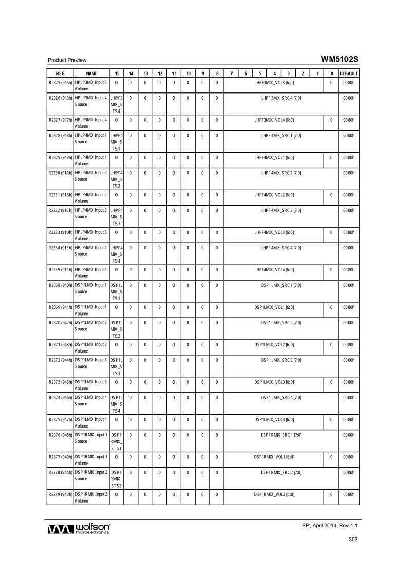
Product Preview WM5102S
w PP, April 2014, Rev 1.1
303
REG NAME 15 14 13 12 11 10 9 8 7 6 5 4 3 2 1 0 DEFAULT
R2325 (915h) HPLP3MIX Input 3 Volume
0 0 0 0 0 0 0 0 LHPF3MIX_VOL3 [6:0] 0 0080h
R2326 (916h) HPLP3MIX Input 4
Source LHPF3MIX_S
TS4
0 0 0 0 0 0 0 LHPF3MIX_SRC4 [7:0] 0000h
R2327 (917h) HPLP3MIX Input 4 Volume
0 0 0 0 0 0 0 0 LHPF3MIX_VOL4 [6:0] 0 0080h
R2328 (918h) HPLP4MIX Input 1
Source LHPF4
MIX_STS1
0 0 0 0 0 0 0 LHPF4MIX_SRC1 [7:0] 0000h
R2329 (919h) HPLP4MIX Input 1 Volume
0 0 0 0 0 0 0 0 LHPF4MIX_VOL1 [6:0] 0 0080h
R2330 (91Ah) HPLP4MIX Input 2
Source LHPF4
MIX_STS2
0 0 0 0 0 0 0 LHPF4MIX_SRC2 [7:0] 0000h
R2331 (91Bh) HPLP4MIX Input 2
Volume 0 0 0 0 0 0 0 0 LHPF4MIX_VOL2 [6:0] 0 0080h
R2332 (91Ch) HPLP4MIX Input 3 Source
LHPF4
MIX_STS3
0 0 0 0 0 0 0 LHPF4MIX_SRC3 [7:0] 0000h
R2333 (91Dh) HPLP4MIX Input 3
Volume 0 0 0 0 0 0 0 0 LHPF4MIX_VOL3 [6:0] 0 0080h
R2334 (91Eh) HPLP4MIX Input 4 Source
LHPF4MIX_S
TS4
0 0 0 0 0 0 0 LHPF4MIX_SRC4 [7:0] 0000h
R2335 (91Fh) HPLP4MIX Input 4 Volume
0 0 0 0 0 0 0 0 LHPF4MIX_VOL4 [6:0] 0 0080h
R2368 (940h) DSP1LMIX Input 1 Source
DSP1LMIX_S
TS1
0 0 0 0 0 0 0 DSP1LMIX_SRC1 [7:0] 0000h
R2369 (941h) DSP1LMIX Input 1 Volume
0 0 0 0 0 0 0 0 DSP1LMIX_VOL1 [6:0] 0 0080h
R2370 (942h) DSP1LMIX Input 2
Source DSP1LMIX_S
TS2
0 0 0 0 0 0 0 DSP1LMIX_SRC2 [7:0] 0000h
R2371 (943h) DSP1LMIX Input 2 Volume
0 0 0 0 0 0 0 0 DSP1LMIX_VOL2 [6:0] 0 0080h
R2372 (944h) DSP1LMIX Input 3
Source DSP1L
MIX_STS3
0 0 0 0 0 0 0 DSP1LMIX_SRC3 [7:0] 0000h
R2373 (945h) DSP1LMIX Input 3
Volume 0 0 0 0 0 0 0 0 DSP1LMIX_VOL3 [6:0] 0 0080h
R2374 (946h) DSP1LMIX Input 4 Source
DSP1L
MIX_STS4
0 0 0 0 0 0 0 DSP1LMIX_SRC4 [7:0] 0000h
R2375 (947h) DSP1LMIX Input 4
Volume 0 0 0 0 0 0 0 0 DSP1LMIX_VOL4 [6:0] 0 0080h
R2376 (948h) DSP1RMIX Input 1 Source
DSP1RMIX_STS1
0 0 0 0 0 0 0 DSP1RMIX_SRC1 [7:0] 0000h
R2377 (949h) DSP1RMIX Input 1 Volume
0 0 0 0 0 0 0 0 DSP1RMIX_VOL1 [6:0] 0 0080h
R2378 (94Ah) DSP1RMIX Input 2 Source
DSP1RMIX_
STS2
0 0 0 0 0 0 0 DSP1RMIX_SRC2 [7:0] 0000h
R2379 (94Bh) DSP1RMIX Input 2 Volume
0 0 0 0 0 0 0 0 DSP1RMIX_VOL2 [6:0] 0 0080h
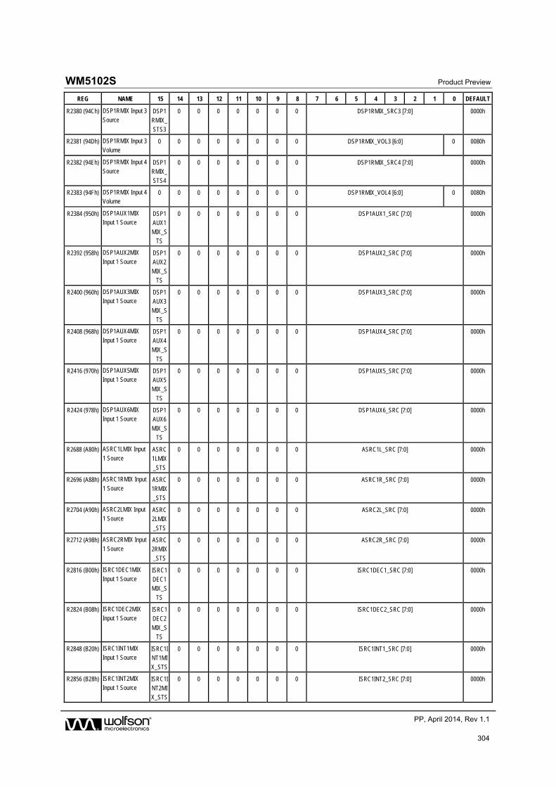
WM5102S Product Preview
w PP, April 2014, Rev 1.1
304
REG NAME 15 14 13 12 11 10 9 8 7 6 5 4 3 2 1 0 DEFAULT
R2380 (94Ch) DSP1RMIX Input 3 Source
DSP1
RMIX_STS3
0 0 0 0 0 0 0 DSP1RMIX_SRC3 [7:0] 0000h
R2381 (94Dh) DSP1RMIX Input 3
Volume 0 0 0 0 0 0 0 0 DSP1RMIX_VOL3 [6:0] 0 0080h
R2382 (94Eh) DSP1RMIX Input 4 Source
DSP1RMIX_STS4
0 0 0 0 0 0 0 DSP1RMIX_SRC4 [7:0] 0000h
R2383 (94Fh) DSP1RMIX Input 4 Volume
0 0 0 0 0 0 0 0 DSP1RMIX_VOL4 [6:0] 0 0080h
R2384 (950h) DSP1AUX1MIX Input 1 Source
DSP1AUX1
MIX_STS
0 0 0 0 0 0 0 DSP1AUX1_SRC [7:0] 0000h
R2392 (958h) DSP1AUX2MIX
Input 1 Source DSP1AUX2
MIX_STS
0 0 0 0 0 0 0 DSP1AUX2_SRC [7:0] 0000h
R2400 (960h) DSP1AUX3MIX
Input 1 Source DSP1
AUX3MIX_S
TS
0 0 0 0 0 0 0 DSP1AUX3_SRC [7:0] 0000h
R2408 (968h) DSP1AUX4MIX Input 1 Source
DSP1
AUX4MIX_S
TS
0 0 0 0 0 0 0 DSP1AUX4_SRC [7:0] 0000h
R2416 (970h) DSP1AUX5MIX Input 1 Source
DSP1AUX5MIX_S
TS
0 0 0 0 0 0 0 DSP1AUX5_SRC [7:0] 0000h
R2424 (978h) DSP1AUX6MIX Input 1 Source
DSP1AUX6
MIX_STS
0 0 0 0 0 0 0 DSP1AUX6_SRC [7:0] 0000h
R2688 (A80h) ASRC1LMIX Input
1 Source ASRC1LMIX
_STS
0 0 0 0 0 0 0 ASRC1L_SRC [7:0] 0000h
R2696 (A88h) ASRC1RMIX Input 1 Source
ASRC1RMIX
_STS
0 0 0 0 0 0 0 ASRC1R_SRC [7:0] 0000h
R2704 (A90h) ASRC2LMIX Input 1 Source
ASRC2LMIX_STS
0 0 0 0 0 0 0 ASRC2L_SRC [7:0] 0000h
R2712 (A98h) ASRC2RMIX Input 1 Source
ASRC
2RMIX_STS
0 0 0 0 0 0 0 ASRC2R_SRC [7:0] 0000h
R2816 (B00h) ISRC1DEC1MIX
Input 1 Source ISRC1
DEC1MIX_S
TS
0 0 0 0 0 0 0 ISRC1DEC1_SRC [7:0] 0000h
R2824 (B08h) ISRC1DEC2MIX Input 1 Source
ISRC1
DEC2MIX_S
TS
0 0 0 0 0 0 0 ISRC1DEC2_SRC [7:0] 0000h
R2848 (B20h) ISRC1INT1MIX Input 1 Source
ISRC1INT1MIX_STS
0 0 0 0 0 0 0 ISRC1INT1_SRC [7:0] 0000h
R2856 (B28h) ISRC1INT2MIX Input 1 Source
ISRC1I
NT2MIX_STS
0 0 0 0 0 0 0 ISRC1INT2_SRC [7:0] 0000h
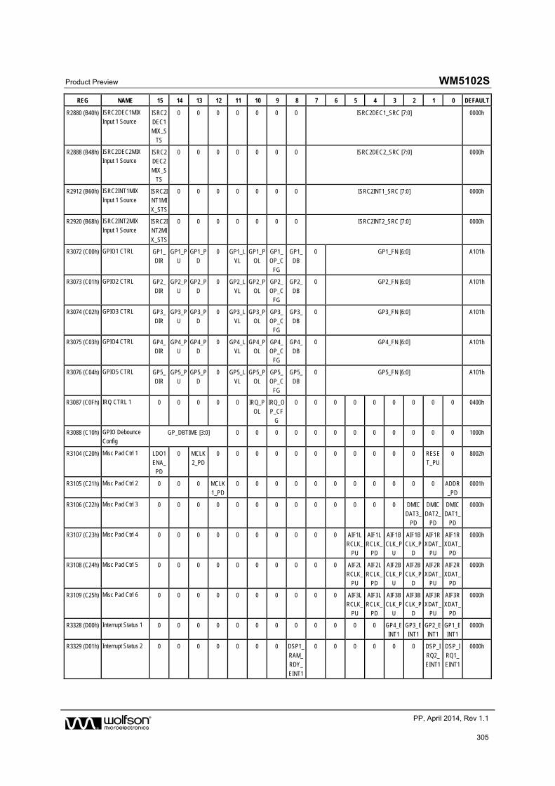
Product Preview WM5102S
w PP, April 2014, Rev 1.1
305
REG NAME 15 14 13 12 11 10 9 8 7 6 5 4 3 2 1 0 DEFAULT
R2880 (B40h) ISRC2DEC1MIX Input 1 Source
ISRC2DEC1MIX_S
TS
0 0 0 0 0 0 0 ISRC2DEC1_SRC [7:0] 0000h
R2888 (B48h) ISRC2DEC2MIX Input 1 Source
ISRC2DEC2
MIX_STS
0 0 0 0 0 0 0 ISRC2DEC2_SRC [7:0] 0000h
R2912 (B60h) ISRC2INT1MIX
Input 1 Source ISRC2INT1MI
X_STS
0 0 0 0 0 0 0 ISRC2INT1_SRC [7:0] 0000h
R2920 (B68h) ISRC2INT2MIX Input 1 Source
ISRC2INT2MI
X_STS
0 0 0 0 0 0 0 ISRC2INT2_SRC [7:0] 0000h
R3072 (C00h) GPIO1 CTRL GP1_DIR
GP1_PU
GP1_PD
0 GP1_LVL
GP1_POL
GP1_OP_C
FG
GP1_DB
0 GP1_FN [6:0] A101h
R3073 (C01h) GPIO2 CTRL GP2_
DIR
GP2_P
U
GP2_P
D
0 GP2_L
VL
GP2_P
OL
GP2_
OP_CFG
GP2_
DB
0 GP2_FN [6:0] A101h
R3074 (C02h) GPIO3 CTRL GP3_
DIR
GP3_P
U
GP3_P
D
0 GP3_L
VL
GP3_P
OL
GP3_
OP_CFG
GP3_
DB
0 GP3_FN [6:0] A101h
R3075 (C03h) GPIO4 CTRL GP4_DIR
GP4_PU
GP4_PD
0 GP4_LVL
GP4_POL
GP4_OP_C
FG
GP4_DB
0 GP4_FN [6:0] A101h
R3076 (C04h) GPIO5 CTRL GP5_DIR
GP5_PU
GP5_PD
0 GP5_LVL
GP5_POL
GP5_OP_C
FG
GP5_DB
0 GP5_FN [6:0] A101h
R3087 (C0Fh) IRQ CTRL 1 0 0 0 0 0 IRQ_P
OL
IRQ_O
P_CFG
0 0 0 0 0 0 0 0 0 0400h
R3088 (C10h) GPIO Debounce
Config GP_DBTIME [3:0] 0 0 0 0 0 0 0 0 0 0 0 0 1000h
R3104 (C20h) Misc Pad Ctrl 1 LDO1ENA_
PD
0 MCLK2_PD
0 0 0 0 0 0 0 0 0 0 0 RESET_PU
0 8002h
R3105 (C21h) Misc Pad Ctrl 2 0 0 0 MCLK
1_PD
0 0 0 0 0 0 0 0 0 0 0 ADDR
_PD
0001h
R3106 (C22h) Misc Pad Ctrl 3 0 0 0 0 0 0 0 0 0 0 0 0 0 DMICDAT3_
PD
DMICDAT2_
PD
DMICDAT1_
PD
0000h
R3107 (C23h) Misc Pad Ctrl 4 0 0 0 0 0 0 0 0 0 0 AIF1LRCLK_
PU
AIF1LRCLK_
PD
AIF1BCLK_P
U
AIF1BCLK_P
D
AIF1RXDAT_
PU
AIF1RXDAT_
PD
0000h
R3108 (C24h) Misc Pad Ctrl 5 0 0 0 0 0 0 0 0 0 0 AIF2L
RCLK_PU
AIF2L
RCLK_PD
AIF2B
CLK_PU
AIF2B
CLK_PD
AIF2R
XDAT_PU
AIF2R
XDAT_PD
0000h
R3109 (C25h) Misc Pad Ctrl 6 0 0 0 0 0 0 0 0 0 0 AIF3L
RCLK_PU
AIF3L
RCLK_PD
AIF3B
CLK_PU
AIF3B
CLK_PD
AIF3R
XDAT_PU
AIF3R
XDAT_PD
0000h
R3328 (D00h) Interrupt Status 1 0 0 0 0 0 0 0 0 0 0 0 0 GP4_EINT1
GP3_EINT1
GP2_EINT1
GP1_EINT1
0000h
R3329 (D01h) Interrupt Status 2 0 0 0 0 0 0 0 DSP1_
RAM_RDY_
EINT1
0 0 0 0 0 0 DSP_I
RQ2_EINT1
DSP_I
RQ1_EINT1
0000h
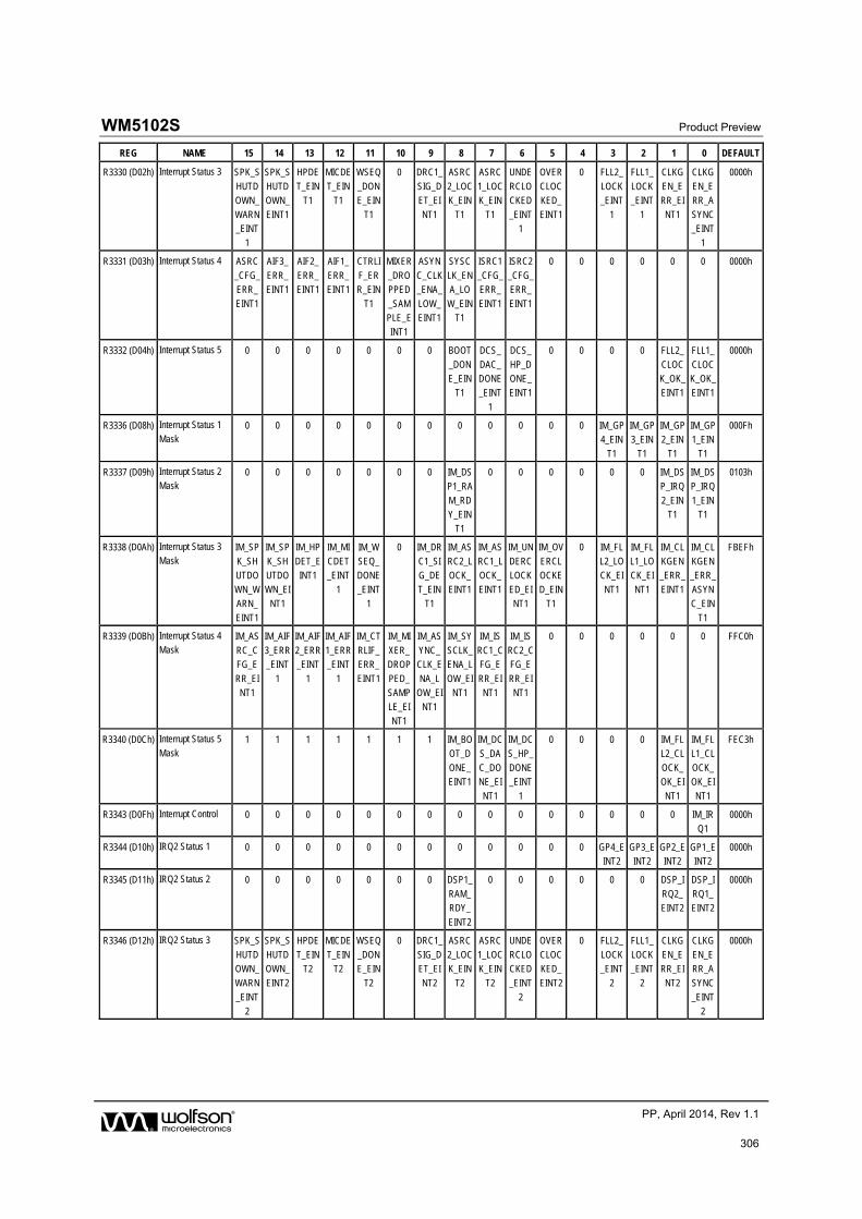
WM5102S Product Preview
w PP, April 2014, Rev 1.1
306
REG NAME 15 14 13 12 11 10 9 8 7 6 5 4 3 2 1 0 DEFAULT
R3330 (D02h) Interrupt Status 3 SPK_S
HUTDOWN_
WARN_EINT
1
SPK_S
HUTDOWN_
EINT1
HPDE
T_EINT1
MICDE
T_EINT1
WSEQ
_DONE_EIN
T1
0 DRC1_
SIG_DET_EI
NT1
ASRC
2_LOCK_EIN
T1
ASRC
1_LOCK_EIN
T1
UNDE
RCLOCKED
_EINT1
OVER
CLOCKED_
EINT1
0 FLL2_
LOCK_EINT
1
FLL1_
LOCK_EINT
1
CLKG
EN_ERR_EI
NT1
CLKG
EN_ERR_A
SYNC_EINT
1
0000h
R3331 (D03h) Interrupt Status 4 ASRC
_CFG_ERR_
EINT1
AIF3_
ERR_EINT1
AIF2_
ERR_EINT1
AIF1_
ERR_EINT1
CTRLI
F_ERR_EIN
T1
MIXER
_DROPPED
_SAMPLE_EINT1
ASYN
C_CLK_ENA_
LOW_EINT1
SYSC
LK_ENA_LO
W_EINT1
ISRC1
_CFG_ERR_
EINT1
ISRC2
_CFG_ERR_
EINT1
0 0 0 0 0 0 0000h
R3332 (D04h) Interrupt Status 5 0 0 0 0 0 0 0 BOOT
_DONE_EIN
T1
DCS_
DAC_DONE
_EINT1
DCS_
HP_DONE_
EINT1
0 0 0 0 FLL2_
CLOCK_OK_
EINT1
FLL1_
CLOCK_OK_
EINT1
0000h
R3336 (D08h) Interrupt Status 1
Mask 0 0 0 0 0 0 0 0 0 0 0 0 IM_GP
4_EIN
T1
IM_GP3_EIN
T1
IM_GP2_EIN
T1
IM_GP1_EIN
T1
000Fh
R3337 (D09h) Interrupt Status 2 Mask
0 0 0 0 0 0 0 IM_DSP1_RA
M_RDY_EIN
T1
0 0 0 0 0 0 IM_DSP_IRQ
2_EINT1
IM_DSP_IRQ
1_EINT1
0103h
R3338 (D0Ah) Interrupt Status 3 Mask
IM_SP
K_SHUTDO
WN_WARN_
EINT1
IM_SP
K_SHUTDO
WN_EINT1
IM_HP
DET_EINT1
IM_MI
CDET_EINT
1
IM_W
SEQ_DONE
_EINT1
0 IM_DR
C1_SIG_DE
T_EINT1
IM_AS
RC2_LOCK_
EINT1
IM_AS
RC1_LOCK_
EINT1
IM_UN
DERCLOCK
ED_EINT1
IM_OV
ERCLOCKE
D_EINT1
0 IM_FL
L2_LOCK_EI
NT1
IM_FL
L1_LOCK_EI
NT1
IM_CL
KGEN_ERR_
EINT1
IM_CL
KGEN_ERR_
ASYNC_EIN
T1
FBEFh
R3339 (D0Bh) Interrupt Status 4 Mask
IM_AS
RC_CFG_E
RR_EINT1
IM_AIF
3_ERR_EINT
1
IM_AIF
2_ERR_EINT
1
IM_AIF
1_ERR_EINT
1
IM_CT
RLIF_ERR_
EINT1
IM_MI
XER_DROP
PED_SAMP
LE_EINT1
IM_AS
YNC_CLK_E
NA_LOW_EI
NT1
IM_SY
SCLK_ENA_L
OW_EINT1
IM_IS
RC1_CFG_E
RR_EINT1
IM_IS
RC2_CFG_E
RR_EINT1
0 0 0 0 0 0 FFC0h
R3340 (D0Ch) Interrupt Status 5
Mask 1 1 1 1 1 1 1 IM_BO
OT_D
ONE_EINT1
IM_DCS_DA
C_DONE_EI
NT1
IM_DCS_HP_
DONE_EINT
1
0 0 0 0 IM_FLL2_CL
OCK_OK_EI
NT1
IM_FLL1_CL
OCK_OK_EI
NT1
FEC3h
R3343 (D0Fh) Interrupt Control 0 0 0 0 0 0 0 0 0 0 0 0 0 0 0 IM_IRQ1
0000h
R3344 (D10h) IRQ2 Status 1 0 0 0 0 0 0 0 0 0 0 0 0 GP4_EINT2
GP3_EINT2
GP2_EINT2
GP1_EINT2
0000h
R3345 (D11h) IRQ2 Status 2 0 0 0 0 0 0 0 DSP1_
RAM_RDY_
EINT2
0 0 0 0 0 0 DSP_I
RQ2_EINT2
DSP_I
RQ1_EINT2
0000h
R3346 (D12h) IRQ2 Status 3 SPK_S
HUTDOWN_
WARN_EINT
2
SPK_S
HUTDOWN_
EINT2
HPDE
T_EINT2
MICDE
T_EINT2
WSEQ
_DONE_EIN
T2
0 DRC1_
SIG_DET_EI
NT2
ASRC
2_LOCK_EIN
T2
ASRC
1_LOCK_EIN
T2
UNDE
RCLOCKED
_EINT2
OVER
CLOCKED_
EINT2
0 FLL2_
LOCK_EINT
2
FLL1_
LOCK_EINT
2
CLKG
EN_ERR_EI
NT2
CLKG
EN_ERR_A
SYNC_EINT
2
0000h
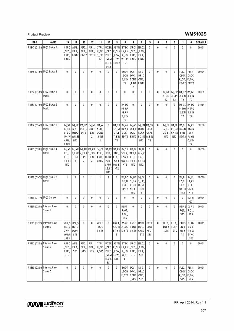
Product Preview WM5102S
w PP, April 2014, Rev 1.1
307
REG NAME 15 14 13 12 11 10 9 8 7 6 5 4 3 2 1 0 DEFAULT
R3347 (D13h) IRQ2 Status 4 ASRC_CFG_ERR_
EINT2
AIF3_ERR_EINT2
AIF2_ERR_EINT2
AIF1_ERR_EINT2
CTRLIF_ERR_EIN
T2
MIXER_DROPPED
_SAMPLE_E
INT2
ASYNC_CLK_ENA_
LOW_EINT2
SYSCLK_ENA_LO
W_EINT2
ISRC1_CFG_ERR_
EINT2
ISRC2_CFG_ERR_
EINT2
0 0 0 0 0 0 0000h
R3348 (D14h) IRQ2 Status 5 0 0 0 0 0 0 0 BOOT_DONE_EIN
T2
DCS_DAC_DONE
_EINT2
DCS_HP_DONE_
EINT2
0 0 0 0 FLL2_CLOCK_OK_
EINT2
FLL1_CLOCK_OK_
EINT2
0000h
R3352 (D18h) IRQ2 Status 1
Mask 0 0 0 0 0 0 0 0 0 0 0 0 IM_GP
4_EINT2
IM_GP
3_EINT2
IM_GP
2_EINT2
IM_GP
1_EINT2
000Fh
R3353 (D19h) IRQ2 Status 2
Mask 0 0 0 0 0 0 0 IM_DS
P1_RA
M_RDY_EIN
T2
0 0 0 0 0 0 IM_DSP_IRQ
2_EINT2
IM_DSP_IRQ
1_EINT2
0103h
R3354 (D1Ah) IRQ2 Status 3 Mask
IM_SPK_SHUTDO
WN_WARN_
EINT2
IM_SPK_SHUTDO
WN_EINT2
IM_HPDET_EINT2
IM_MICDET_EINT
2
IM_WSEQ_DONE
_EINT2
0 IM_DRC1_SIG_DE
T_EINT2
IM_ASRC2_LOCK_
EINT2
IM_ASRC1_LOCK_
EINT2
IM_UNDERCLOCK
ED_EINT2
IM_OVERCLOCKE
D_EINT2
0 IM_FLL2_LOCK_EI
NT2
IM_FLL1_LOCK_EI
NT2
IM_CLKGEN_ERR_
EINT2
IM_CLKGEN_ERR_
ASYNC_EIN
T2
FFEFh
R3355 (D1Bh) IRQ2 Status 4 Mask
IM_ASRC_CFG_E
RR_EINT2
IM_AIF3_ERR_EINT
2
IM_AIF2_ERR_EINT
2
IM_AIF1_ERR_EINT
2
IM_CTRLIF_ERR_
EINT2
IM_MIXER_DROP
PED_SAMP
LE_EINT2
IM_ASYNC_CLK_E
NA_LOW_EI
NT2
IM_SYSCLK_ENA_L
OW_EINT2
IM_ISRC1_CFG_E
RR_EINT2
IM_ISRC2_CFG_E
RR_EINT2
0 0 0 0 0 0 FFC0h
R3356 (D1Ch) IRQ2 Status 5
Mask 1 1 1 1 1 1 1 IM_BO
OT_D
ONE_EINT2
IM_DCS_DA
C_DONE_EI
NT2
IM_DCS_HP_
DONE_EINT
2
0 0 0 0 IM_FLL2_CL
OCK_OK_EI
NT2
IM_FLL1_CL
OCK_OK_EI
NT2
FEC3h
R3359 (D1Fh) IRQ2 Control 0 0 0 0 0 0 0 0 0 0 0 0 0 0 0 IM_IRQ2
0000h
R3360 (D20h) Interrupt Raw
Status 2 0 0 0 0 0 0 0 DSP1_
RAM_
RDY_STS
0 0 0 0 0 0 DSP_IRQ2_
STS
DSP_IRQ1_
STS
0000h
R3361 (D21h) Interrupt Raw
Status 3 SPK_S
HUTDOWN_WARN
_STS
SPK_S
HUTDOWN_STS
0 0 WSEQ
_DONE_STS
0 DRC1_
SIG_DET_ST
S
ASRC
2_LOCK_STS
ASRC
1_LOCK_STS
UNDE
RCLOCKED_STS
OVER
CLOCKED_STS
0 FLL2_
LOCK_STS
FLL1_
LOCK_STS
CLKG
EN_ERR_S
TS
CLKG
EN_ERR_ASYNC
_STS
0000h
R3362 (D22h) Interrupt Raw Status 4
ASRC_CFG_
ERR_STS
AIF3_ERR_
STS
AIF2_ERR_
STS
AIF1_ERR_
STS
CTRLIF_ER
R_STS
MIXER_DRO
PPED_SAMPLE_S
TS
ASYNC_CLK
_ENA_LOW_STS
SYSCLK_EN
A_LOW_ST
S
ISRC1_CFG_
ERR_STS
ISRC2_CFG_
ERR_STS
0 0 0 0 0 0 0000h
R3363 (D23h) Interrupt Raw Status 5
0 0 0 0 0 0 0 BOOT_DON
E_STS
DCS_DAC_
DONE_STS
DCS_HP_D
ONE_STS
0 0 0 0 FLL2_CLOC
K_OK_STS
FLL1_CLOC
K_OK_STS
0000h
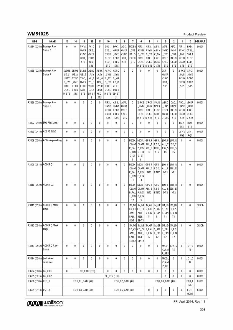
WM5102S Product Preview
w PP, April 2014, Rev 1.1
308
REG NAME 15 14 13 12 11 10 9 8 7 6 5 4 3 2 1 0 DEFAULT
R3364 (D24h) Interrupt Raw Status 6
0 0 PWM_
OVERCLOC
KED_STS
FX_C
ORE_OVER
CLOCKED_STS
0 DAC_
SYS_OVER
CLOCKED_STS
DAC_
WARP_OVE
RCLOCKED_STS
ADC_
OVERCLOC
KED_STS
MIXER
_OVERCLO
CKED_STS
AIF3_
ASYNC_OV
ERCLOCKED_STS
AIF2_
ASYNC_OV
ERCLOCKED_STS
AIF1_
ASYNC_OV
ERCLOCKED_STS
AIF3_
SYNC_OVE
RCLOCKED_STS
AIF2_
SYNC_OVE
RCLOCKED_STS
AIF1_
SYNC_OVE
RCLOCKED_STS
PAD_
CTRL_OVER
CLOCKED_STS
0000h
R3365 (D25h) Interrupt Raw Status 7
SLIMB
US_SUBSY
S_OVERCLOCKE
D_STS
SLIMB
US_ASYNC
_OVERCLOCKED
_STS
SLIMB
US_SYNC_
OVERCLOCKED_
STS
ASRC
_ASYNC_S
YS_OVERCLOCK
ED_STS
ASRC
_ASYNC_W
ARP_OVERCLOC
KED_STS
ASRC
_SYNC_SY
S_OVERCLOCKE
D_STS
ASRC
_SYNC_WA
RP_OVERCLOCK
ED_STS
0 0 0 0 0 DSP1_
OVERCLOC
KED_STS
0 ISRC2
_OVERCLO
CKED_STS
ISRC1
_OVERCLO
CKED_STS
0000h
R3366 (D26h) Interrupt Raw
Status 8 0 0 0 0 0 AIF3_
UNDERCLO
CKED_STS
AIF2_
UNDERCLO
CKED_STS
AIF1_
UNDERCLO
CKED_STS
0 ISRC2
_UNDERCL
OCKED_STS
ISRC1
_UNDERCL
OCKED_STS
FX_U
NDERCLOC
KED_STS
ASRC
_UNDERCL
OCKED_STS
DAC_
UNDERCLO
CKED_STS
ADC_
UNDERCLO
CKED_STS
MIXER
_UNDERCL
OCKED_STS
0000h
R3392 (D40h) IRQ Pin Status 0 0 0 0 0 0 0 0 0 0 0 0 0 0 IRQ2_STS
IRQ1_STS
0000h
R3393 (D41h) ADSP2 IRQ0 0 0 0 0 0 0 0 0 0 0 0 0 0 0 DSP_I
RQ2
DSP_I
RQ1
0000h
R3408 (D50h) AOD wkup and trig 0 0 0 0 0 0 0 0 MICD_CLAMP_FAL
L_TRIG_ST
S
MICD_CLAMP_RIS
E_TRIG_ST
S
GP5_FALL_TRIG_S
TS
GP5_RISE_TRIG_
STS
JD1_FALL_TRIG_S
TS
JD1_RISE_TRIG_S
TS
0 0 0000h
R3409 (D51h) AOD IRQ1 0 0 0 0 0 0 0 0 MICD_CLAMP_FAL
L_EINT1
MICD_CLAMP_RIS
E_EINT1
GP5_FALL_EINT1
GP5_RISE_EINT1
JD1_FALL_EINT1
JD1_RISE_EI
NT1
0 0 0000h
R3410 (D52h) AOD IRQ2 0 0 0 0 0 0 0 0 MICD_
CLAMP_FAL
L_EINT2
MICD_
CLAMP_RIS
E_EINT2
GP5_F
ALL_EINT2
GP5_
RISE_EINT2
JD1_F
ALL_EINT2
JD1_R
ISE_EINT2
0 0 0000h
R3411 (D53h) AOD IRQ Mask IRQ1
0 0 0 0 0 0 0 0 IM_MICD_CL
AMP_FALL_
EINT1
IM_MICD_CL
AMP_RISE_
EINT1
IM_GP5_FAL
L_EINT1
IM_GP5_RIS
E_EINT1
IM_JD1_FAL
L_EINT1
IM_JD1_RIS
E_EINT1
0 0 003Ch
R3412 (D54h) AOD IRQ Mask IRQ2
0 0 0 0 0 0 0 0 IM_MICD_CLAMP_
FALL_EINT2
IM_MICD_CLAMP_
RISE_EINT2
IM_GP5_FALL_EIN
T2
IM_GP5_RISE_EIN
T2
IM_JD1_FALL_EIN
T2
IM_JD1_RISE_EIN
T2
0 0 003Ch
R3413 (D55h) AOD IRQ Raw
Status 0 0 0 0 0 0 0 0 0 0 0 0 MICD_
CLAMP_STS
GP5_S
TS
0 JD1_S
TS
0000h
R3414 (D56h) Jack detect
debounce 0 0 0 0 0 0 0 0 0 0 0 0 MICD_
CLAM
P_DB
0 0 JD1_DB
0000h
R3584 (E00h) FX_Ctrl1 0 FX_RATE [3:0] 0 0 0 0 0 0 0 0 0 0 0 0000h
R3585 (E01h) FX_Ctrl2 FX_STS [11:0] 0 0 0 0 0000h
R3600 (E10h) EQ1_1 EQ1_B1_GAIN [4:0] EQ1_B2_GAIN [4:0] EQ1_B3_GAIN [4:0] EQ1_ENA
6318h
R3601 (E11h) EQ1_2 EQ1_B4_GAIN [4:0] EQ1_B5_GAIN [4:0] 0 0 0 0 0 EQ1_MODE
6300h
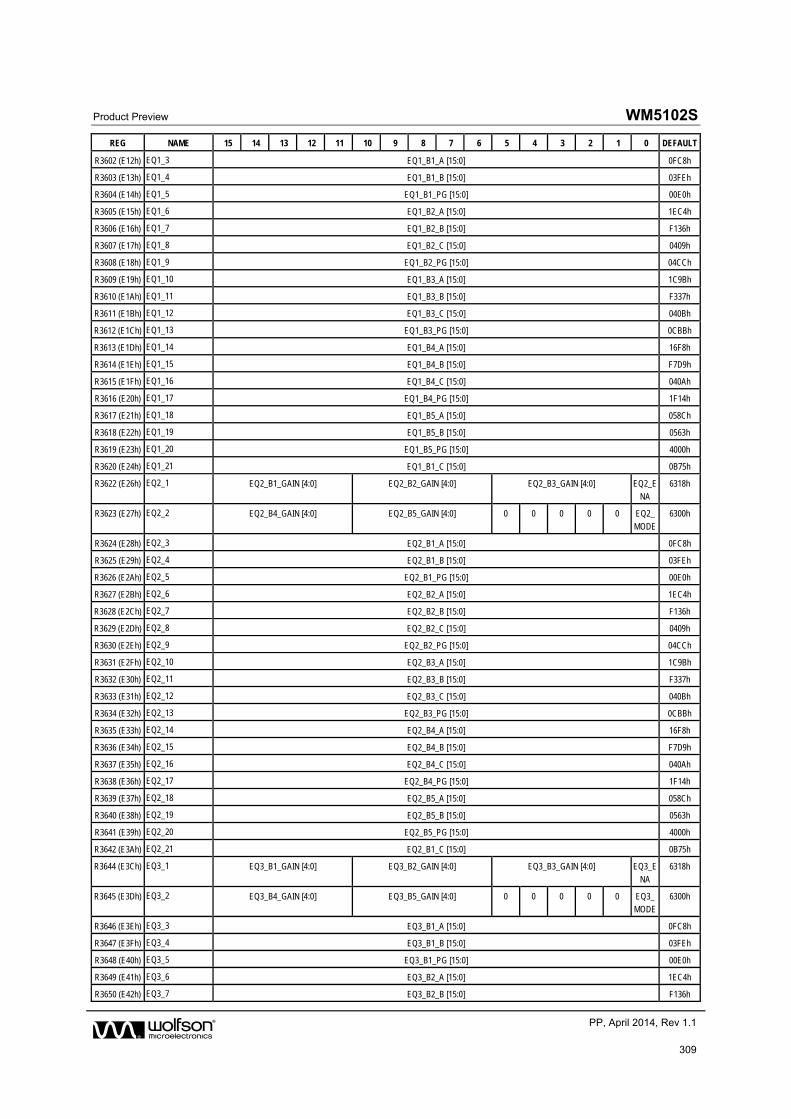
Product Preview WM5102S
w PP, April 2014, Rev 1.1
309
REG NAME 15 14 13 12 11 10 9 8 7 6 5 4 3 2 1 0 DEFAULT
R3602 (E12h) EQ1_3 EQ1_B1_A [15:0] 0FC8h
R3603 (E13h) EQ1_4 EQ1_B1_B [15:0] 03FEh
R3604 (E14h) EQ1_5 EQ1_B1_PG [15:0] 00E0h
R3605 (E15h) EQ1_6 EQ1_B2_A [15:0] 1EC4h
R3606 (E16h) EQ1_7 EQ1_B2_B [15:0] F136h
R3607 (E17h) EQ1_8 EQ1_B2_C [15:0] 0409h
R3608 (E18h) EQ1_9 EQ1_B2_PG [15:0] 04CCh
R3609 (E19h) EQ1_10 EQ1_B3_A [15:0] 1C9Bh
R3610 (E1Ah) EQ1_11 EQ1_B3_B [15:0] F337h
R3611 (E1Bh) EQ1_12 EQ1_B3_C [15:0] 040Bh
R3612 (E1Ch) EQ1_13 EQ1_B3_PG [15:0] 0CBBh
R3613 (E1Dh) EQ1_14 EQ1_B4_A [15:0] 16F8h
R3614 (E1Eh) EQ1_15 EQ1_B4_B [15:0] F7D9h
R3615 (E1Fh) EQ1_16 EQ1_B4_C [15:0] 040Ah
R3616 (E20h) EQ1_17 EQ1_B4_PG [15:0] 1F14h
R3617 (E21h) EQ1_18 EQ1_B5_A [15:0] 058Ch
R3618 (E22h) EQ1_19 EQ1_B5_B [15:0] 0563h
R3619 (E23h) EQ1_20 EQ1_B5_PG [15:0] 4000h
R3620 (E24h) EQ1_21 EQ1_B1_C [15:0] 0B75h
R3622 (E26h) EQ2_1 EQ2_B1_GAIN [4:0] EQ2_B2_GAIN [4:0] EQ2_B3_GAIN [4:0] EQ2_E
NA
6318h
R3623 (E27h) EQ2_2 EQ2_B4_GAIN [4:0] EQ2_B5_GAIN [4:0] 0 0 0 0 0 EQ2_
MODE 6300h
R3624 (E28h) EQ2_3 EQ2_B1_A [15:0] 0FC8h
R3625 (E29h) EQ2_4 EQ2_B1_B [15:0] 03FEh
R3626 (E2Ah) EQ2_5 EQ2_B1_PG [15:0] 00E0h
R3627 (E2Bh) EQ2_6 EQ2_B2_A [15:0] 1EC4h
R3628 (E2Ch) EQ2_7 EQ2_B2_B [15:0] F136h
R3629 (E2Dh) EQ2_8 EQ2_B2_C [15:0] 0409h
R3630 (E2Eh) EQ2_9 EQ2_B2_PG [15:0] 04CCh
R3631 (E2Fh) EQ2_10 EQ2_B3_A [15:0] 1C9Bh
R3632 (E30h) EQ2_11 EQ2_B3_B [15:0] F337h
R3633 (E31h) EQ2_12 EQ2_B3_C [15:0] 040Bh
R3634 (E32h) EQ2_13 EQ2_B3_PG [15:0] 0CBBh
R3635 (E33h) EQ2_14 EQ2_B4_A [15:0] 16F8h
R3636 (E34h) EQ2_15 EQ2_B4_B [15:0] F7D9h
R3637 (E35h) EQ2_16 EQ2_B4_C [15:0] 040Ah
R3638 (E36h) EQ2_17 EQ2_B4_PG [15:0] 1F14h
R3639 (E37h) EQ2_18 EQ2_B5_A [15:0] 058Ch
R3640 (E38h) EQ2_19 EQ2_B5_B [15:0] 0563h
R3641 (E39h) EQ2_20 EQ2_B5_PG [15:0] 4000h
R3642 (E3Ah) EQ2_21 EQ2_B1_C [15:0] 0B75h
R3644 (E3Ch) EQ3_1 EQ3_B1_GAIN [4:0] EQ3_B2_GAIN [4:0] EQ3_B3_GAIN [4:0] EQ3_E
NA
6318h
R3645 (E3Dh) EQ3_2 EQ3_B4_GAIN [4:0] EQ3_B5_GAIN [4:0] 0 0 0 0 0 EQ3_MODE
6300h
R3646 (E3Eh) EQ3_3 EQ3_B1_A [15:0] 0FC8h
R3647 (E3Fh) EQ3_4 EQ3_B1_B [15:0] 03FEh
R3648 (E40h) EQ3_5 EQ3_B1_PG [15:0] 00E0h
R3649 (E41h) EQ3_6 EQ3_B2_A [15:0] 1EC4h
R3650 (E42h) EQ3_7 EQ3_B2_B [15:0] F136h
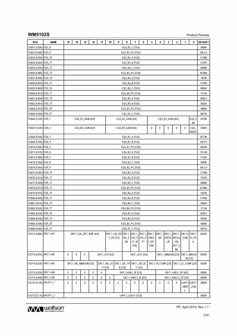
WM5102S Product Preview
w PP, April 2014, Rev 1.1
310
REG NAME 15 14 13 12 11 10 9 8 7 6 5 4 3 2 1 0 DEFAULT
R3651 (E43h) EQ3_8 EQ3_B2_C [15:0] 0409h
R3652 (E44h) EQ3_9 EQ3_B2_PG [15:0] 04CCh
R3653 (E45h) EQ3_10 EQ3_B3_A [15:0] 1C9Bh
R3654 (E46h) EQ3_11 EQ3_B3_B [15:0] F337h
R3655 (E47h) EQ3_12 EQ3_B3_C [15:0] 040Bh
R3656 (E48h) EQ3_13 EQ3_B3_PG [15:0] 0CBBh
R3657 (E49h) EQ3_14 EQ3_B4_A [15:0] 16F8h
R3658 (E4Ah) EQ3_15 EQ3_B4_B [15:0] F7D9h
R3659 (E4Bh) EQ3_16 EQ3_B4_C [15:0] 040Ah
R3660 (E4Ch) EQ3_17 EQ3_B4_PG [15:0] 1F14h
R3661 (E4Dh) EQ3_18 EQ3_B5_A [15:0] 058Ch
R3662 (E4Eh) EQ3_19 EQ3_B5_B [15:0] 0563h
R3663 (E4Fh) EQ3_20 EQ3_B5_PG [15:0] 4000h
R3664 (E50h) EQ3_21 EQ3_B1_C [15:0] 0B75h
R3666 (E52h) EQ4_1 EQ4_B1_GAIN [4:0] EQ4_B2_GAIN [4:0] EQ4_B3_GAIN [4:0] EQ4_E
NA
6318h
R3667 (E53h) EQ4_2 EQ4_B4_GAIN [4:0] EQ4_B5_GAIN [4:0] 0 0 0 0 0 EQ4_MODE
6300h
R3668 (E54h) EQ4_3 EQ4_B1_A [15:0] 0FC8h
R3669 (E55h) EQ4_4 EQ4_B1_B [15:0] 03FEh
R3670 (E56h) EQ4_5 EQ4_B1_PG [15:0] 00E0h
R3671 (E57h) EQ4_6 EQ4_B2_A [15:0] 1EC4h
R3672 (E58h) EQ4_7 EQ4_B2_B [15:0] F136h
R3673 (E59h) EQ4_8 EQ4_B2_C [15:0] 0409h
R3674 (E5Ah) EQ4_9 EQ4_B2_PG [15:0] 04CCh
R3675 (E5Bh) EQ4_10 EQ4_B3_A [15:0] 1C9Bh
R3676 (E5Ch) EQ4_11 EQ4_B3_B [15:0] F337h
R3677 (E5Dh) EQ4_12 EQ4_B3_C [15:0] 040Bh
R3678 (E5Eh) EQ4_13 EQ4_B3_PG [15:0] 0CBBh
R3679 (E5Fh) EQ4_14 EQ4_B4_A [15:0] 16F8h
R3680 (E60h) EQ4_15 EQ4_B4_B [15:0] F7D9h
R3681 (E61h) EQ4_16 EQ4_B4_C [15:0] 040Ah
R3682 (E62h) EQ4_17 EQ4_B4_PG [15:0] 1F14h
R3683 (E63h) EQ4_18 EQ4_B5_A [15:0] 058Ch
R3684 (E64h) EQ4_19 EQ4_B5_B [15:0] 0563h
R3685 (E65h) EQ4_20 EQ4_B5_PG [15:0] 4000h
R3686 (E66h) EQ4_21 EQ4_B1_C [15:0] 0B75h
R3712 (E80h) DRC1 ctrl1 DRC1_SIG_DET_RMS [4:0] DRC1_SIG_DE
T_PK [1:0]
DRC1_
NG_ENA
DRC1_
SIG_DET_M
ODE
DRC1_
SIG_DET
DRC1_
KNEE2_OP_
ENA
DRC1_
QR
DRC1_
ANTICLIP
DRC1_
WSEQ_SIG_
DET_ENA
DRC1L
_ENA
DRC1
R_ENA
0018h
R3713 (E81h) DRC1 ctrl2 0 0 0 DRC1_ATK [3:0] DRC1_DCY [3:0] DRC1_MINGAIN [2:0] DRC1_MAXGAIN [1:0]
0933h
R3714 (E82h) DRC1 ctrl3 DRC1_NG_MINGAIN [3:0] DRC1_NG_EX
P [1:0]
DRC1_QR_TH
R [1:0]
DRC1_QR_DC
Y [1:0]
DRC1_HI_COMP [2:0] DRC1_LO_COMP [2:0] 0018h
R3715 (E83h) DRC1 ctrl4 0 0 0 0 0 DRC1_KNEE_IP [5:0] DRC1_KNEE_OP [4:0] 0000h
R3716 (E84h) DRC1 ctrl5 0 0 0 0 0 0 DRC1_KNEE2_IP [4:0] DRC1_KNEE2_OP [4:0] 0000h
R3776 (EC0h) HPLPF1_1 0 0 0 0 0 0 0 0 0 0 0 0 0 0 LHPF1_MOD
E
LHPF1_ENA
0000h
R3777 (EC1h) HPLPF1_2 LHPF1_COEFF [15:0] 0000h
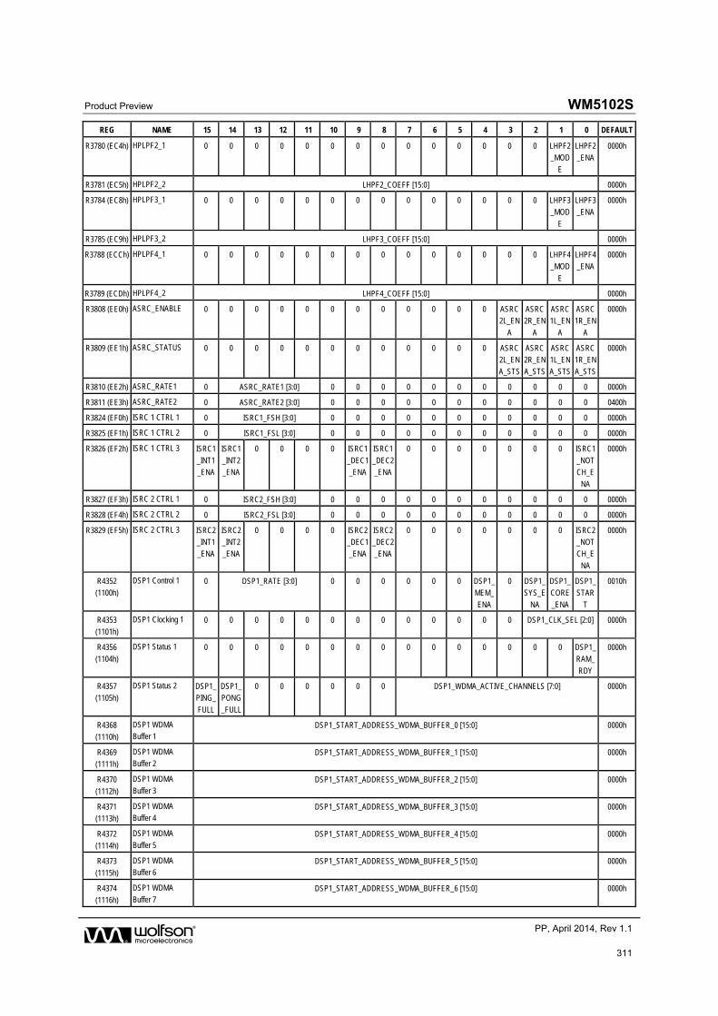
Product Preview WM5102S
w PP, April 2014, Rev 1.1
311
REG NAME 15 14 13 12 11 10 9 8 7 6 5 4 3 2 1 0 DEFAULT
R3780 (EC4h) HPLPF2_1 0 0 0 0 0 0 0 0 0 0 0 0 0 0 LHPF2_MOD
E
LHPF2_ENA
0000h
R3781 (EC5h) HPLPF2_2 LHPF2_COEFF [15:0] 0000h
R3784 (EC8h) HPLPF3_1 0 0 0 0 0 0 0 0 0 0 0 0 0 0 LHPF3
_MODE
LHPF3
_ENA 0000h
R3785 (EC9h) HPLPF3_2 LHPF3_COEFF [15:0] 0000h
R3788 (ECCh) HPLPF4_1 0 0 0 0 0 0 0 0 0 0 0 0 0 0 LHPF4_MOD
E
LHPF4_ENA
0000h
R3789 (ECDh) HPLPF4_2 LHPF4_COEFF [15:0] 0000h
R3808 (EE0h) ASRC_ENABLE 0 0 0 0 0 0 0 0 0 0 0 0 ASRC2L_EN
A
ASRC2R_EN
A
ASRC1L_EN
A
ASRC1R_EN
A
0000h
R3809 (EE1h) ASRC_STATUS 0 0 0 0 0 0 0 0 0 0 0 0 ASRC2L_ENA_STS
ASRC2R_ENA_STS
ASRC1L_ENA_STS
ASRC1R_ENA_STS
0000h
R3810 (EE2h) ASRC_RATE1 0 ASRC_RATE1 [3:0] 0 0 0 0 0 0 0 0 0 0 0 0000h
R3811 (EE3h) ASRC_RATE2 0 ASRC_RATE2 [3:0] 0 0 0 0 0 0 0 0 0 0 0 0400h
R3824 (EF0h) ISRC 1 CTRL 1 0 ISRC1_FSH [3:0] 0 0 0 0 0 0 0 0 0 0 0 0000h
R3825 (EF1h) ISRC 1 CTRL 2 0 ISRC1_FSL [3:0] 0 0 0 0 0 0 0 0 0 0 0 0000h
R3826 (EF2h) ISRC 1 CTRL 3 ISRC1
_INT1_ENA
ISRC1
_INT2_ENA
0 0 0 0 ISRC1
_DEC1_ENA
ISRC1
_DEC2_ENA
0 0 0 0 0 0 0 ISRC1
_NOTCH_E
NA
0000h
R3827 (EF3h) ISRC 2 CTRL 1 0 ISRC2_FSH [3:0] 0 0 0 0 0 0 0 0 0 0 0 0000h
R3828 (EF4h) ISRC 2 CTRL 2 0 ISRC2_FSL [3:0] 0 0 0 0 0 0 0 0 0 0 0 0000h
R3829 (EF5h) ISRC 2 CTRL 3 ISRC2
_INT1_ENA
ISRC2
_INT2_ENA
0 0 0 0 ISRC2
_DEC1_ENA
ISRC2
_DEC2_ENA
0 0 0 0 0 0 0 ISRC2
_NOTCH_E
NA
0000h
R4352 (1100h)
DSP1 Control 1 0 DSP1_RATE [3:0] 0 0 0 0 0 0 DSP1_MEM_
ENA
0 DSP1_SYS_E
NA
DSP1_CORE
_ENA
DSP1_STAR
T
0010h
R4353
(1101h)
DSP1 Clocking 1 0 0 0 0 0 0 0 0 0 0 0 0 0 DSP1_CLK_SEL [2:0] 0000h
R4356 (1104h)
DSP1 Status 1 0 0 0 0 0 0 0 0 0 0 0 0 0 0 0 DSP1_RAM_
RDY
0000h
R4357 (1105h)
DSP1 Status 2 DSP1_PING_FULL
DSP1_PONG_FULL
0 0 0 0 0 0 DSP1_WDMA_ACTIVE_CHANNELS [7:0] 0000h
R4368
(1110h)
DSP1 WDMA Buffer 1
DSP1_START_ADDRESS_WDMA_BUFFER_0 [15:0] 0000h
R4369 (1111h)
DSP1 WDMA Buffer 2
DSP1_START_ADDRESS_WDMA_BUFFER_1 [15:0] 0000h
R4370
(1112h)
DSP1 WDMA
Buffer 3 DSP1_START_ADDRESS_WDMA_BUFFER_2 [15:0] 0000h
R4371 (1113h)
DSP1 WDMA Buffer 4
DSP1_START_ADDRESS_WDMA_BUFFER_3 [15:0] 0000h
R4372 (1114h)
DSP1 WDMA
Buffer 5 DSP1_START_ADDRESS_WDMA_BUFFER_4 [15:0] 0000h
R4373
(1115h)
DSP1 WDMA Buffer 6
DSP1_START_ADDRESS_WDMA_BUFFER_5 [15:0] 0000h
R4374 (1116h)
DSP1 WDMA Buffer 7
DSP1_START_ADDRESS_WDMA_BUFFER_6 [15:0] 0000h
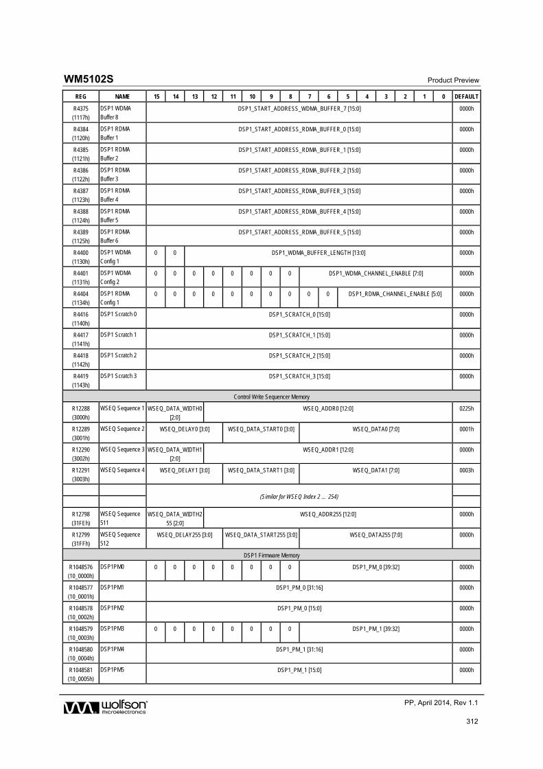
WM5102S Product Preview
w PP, April 2014, Rev 1.1
312
REG NAME 15 14 13 12 11 10 9 8 7 6 5 4 3 2 1 0 DEFAULT
R4375
(1117h)
DSP1 WDMA Buffer 8
DSP1_START_ADDRESS_WDMA_BUFFER_7 [15:0] 0000h
R4384 (1120h)
DSP1 RDMA Buffer 1
DSP1_START_ADDRESS_RDMA_BUFFER_0 [15:0] 0000h
R4385
(1121h)
DSP1 RDMA
Buffer 2 DSP1_START_ADDRESS_RDMA_BUFFER_1 [15:0] 0000h
R4386 (1122h)
DSP1 RDMA Buffer 3
DSP1_START_ADDRESS_RDMA_BUFFER_2 [15:0] 0000h
R4387 (1123h)
DSP1 RDMA
Buffer 4 DSP1_START_ADDRESS_RDMA_BUFFER_3 [15:0] 0000h
R4388
(1124h)
DSP1 RDMA Buffer 5
DSP1_START_ADDRESS_RDMA_BUFFER_4 [15:0] 0000h
R4389 (1125h)
DSP1 RDMA Buffer 6
DSP1_START_ADDRESS_RDMA_BUFFER_5 [15:0] 0000h
R4400
(1130h)
DSP1 WDMA
Config 1 0 0 DSP1_WDMA_BUFFER_LENGTH [13:0] 0000h
R4401 (1131h)
DSP1 WDMA Config 2
0 0 0 0 0 0 0 0 DSP1_WDMA_CHANNEL_ENABLE [7:0] 0000h
R4404 (1134h)
DSP1 RDMA
Config 1 0 0 0 0 0 0 0 0 0 0 DSP1_RDMA_CHANNEL_ENABLE [5:0] 0000h
R4416
(1140h)
DSP1 Scratch 0 DSP1_SCRATCH_0 [15:0] 0000h
R4417 (1141h)
DSP1 Scratch 1 DSP1_SCRATCH_1 [15:0] 0000h
R4418 (1142h)
DSP1 Scratch 2 DSP1_SCRATCH_2 [15:0] 0000h
R4419
(1143h)
DSP1 Scratch 3 DSP1_SCRATCH_3 [15:0] 0000h
Control Write Sequencer Memory
R12288 (3000h)
WSEQ Sequence 1 WSEQ_DATA_WIDTH0 [2:0]
WSEQ_ADDR0 [12:0] 0225h
R12289
(3001h)
WSEQ Sequence 2 WSEQ_DELAY0 [3:0] WSEQ_DATA_START0 [3:0] WSEQ_DATA0 [7:0] 0001h
R12290 (3002h)
WSEQ Sequence 3 WSEQ_DATA_WIDTH1 [2:0]
WSEQ_ADDR1 [12:0] 0000h
R12291 (3003h)
WSEQ Sequence 4 WSEQ_DELAY1 [3:0] WSEQ_DATA_START1 [3:0] WSEQ_DATA1 [7:0] 0003h
(Similar for WSEQ Index 2 … 254)
R12798
(31FEh)
WSEQ Sequence
511 WSEQ_DATA_WIDTH2
55 [2:0]
WSEQ_ADDR255 [12:0] 0000h
R12799 (31FFh)
WSEQ Sequence 512
WSEQ_DELAY255 [3:0] WSEQ_DATA_START255 [3:0] WSEQ_DATA255 [7:0] 0000h
DSP1 Firmware Memory
R1048576 (10_0000h)
DSP1PM0 0 0 0 0 0 0 0 0 DSP1_PM_0 [39:32] 0000h
R1048577
(10_0001h)
DSP1PM1 DSP1_PM_0 [31:16] 0000h
R1048578 (10_0002h)
DSP1PM2 DSP1_PM_0 [15:0] 0000h
R1048579
(10_0003h)
DSP1PM3 0 0 0 0 0 0 0 0 DSP1_PM_1 [39:32] 0000h
R1048580 (10_0004h)
DSP1PM4 DSP1_PM_1 [31:16] 0000h
R1048581 (10_0005h)
DSP1PM5 DSP1_PM_1 [15:0] 0000h
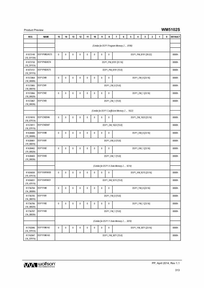
Product Preview WM5102S
w PP, April 2014, Rev 1.1
313
REG NAME 15 14 13 12 11 10 9 8 7 6 5 4 3 2 1 0 DEFAULT
(Similar for DSP1 Program Memory 2 … 8190)
R1073149
(10_5FFDh)
DSP1PM024573 0 0 0 0 0 0 0 0 DSP1_PM_8191 [39:32] 0000h
R1073150 (10_5FFEh)
DSP1PM24574 DSP1_PM_8191 [31:16] 0000h
R1073151
(10_5FFFh)
DSP1PM24575 DSP1_PM_8191 [15:0] 0000h
R1572864
(18_0000h)
DSP1ZM0 0 0 0 0 0 0 0 0 DSP1_ZM_0 [23:16] 0000h
R1572865 (18_0001h)
DSP1ZM1 DSP1_ZM_0 [15:0] 0000h
R1572866
(18_0002h)
DSP1ZM2 0 0 0 0 0 0 0 0 DSP1_ZM_1 [23:16] 0000h
R1572867 (18_0003h)
DSP1ZM3 DSP1_ZM_1 [15:0] 0000h
(Similar for DSP1 Coefficient Memory 2 … 1022)
R1574910 (18_07FEh)
DSP1ZM2046 0 0 0 0 0 0 0 0 DSP1_ZM_1023 [23:16] 0000h
R1574911
(18_07FFh)
DSP1ZM2047 DSP1_ZM_1023 [15:0] 0000h
R1638400
(19_0000h)
DSP1XM0 0 0 0 0 0 0 0 0 DSP1_XM_0 [23:16] 0000h
R1638401 (19_0001h)
DSP1XM1 DSP1_XM_0 [15:0] 0000h
R1638402
(19_0002h)
DSP1XM2 0 0 0 0 0 0 0 0 DSP1_XM_1 [23:16] 0000h
R1638403 (19_0003h)
DSP1XM3 DSP1_XM_1 [15:0] 0000h
(Similar for DSP1 X Data Memory 2 … 9214)
R1656830 (19_47FEh)
DSP1XM18430 0 0 0 0 0 0 0 0 DSP1_XM_9215 [23:16] 0000h
R1656831
(19_47FFh)
DSP1XM18431 DSP1_XM_9215 [15:0] 0000h
R1736704
(1A_8000h)
DSP1YM0 0 0 0 0 0 0 0 0 DSP1_YM_0 [23:16] 0000h
R1736705 (1A_8001h)
DSP1YM1 DSP1_YM_0 [15:0] 0000h
R1736706
(1A_8002h)
DSP1YM2 0 0 0 0 0 0 0 0 DSP1_YM_1 [23:16] 0000h
R1736707 (1A_8003h)
DSP1YM3 DSP1_YM_1 [15:0] 0000h
(Similar for DSP1 Y Data Memory 2 … 3070)
R1742846 (1A_97FEh)
DSP1YM6142 0 0 0 0 0 0 0 0 DSP1_YM_3071 [23:16] 0000h
R1742847
(1A_97FFh)
DSP1YM6143 DSP1_YM_3071 [15:0] 0000h
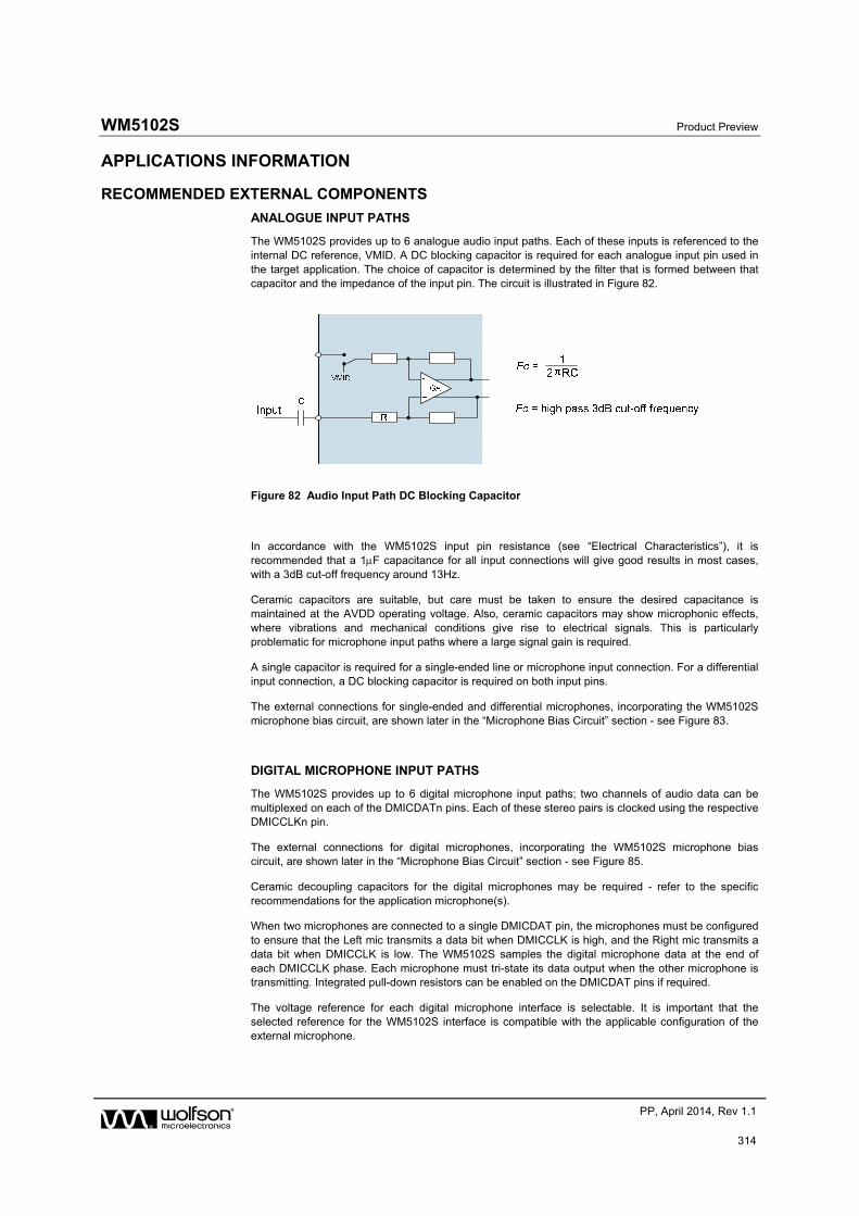
WM5102S Product Preview
w PP, April 2014, Rev 1.1
314
APPLICATIONS INFORMATION
RECOMMENDED EXTERNAL COMPONENTS
ANALOGUE INPUT PATHS
The WM5102S provides up to 6 analogue audio input paths. Each of these inputs is referenced to the internal DC reference, VMID. A DC blocking capacitor is required for each analogue input pin used in the target application. The choice of capacitor is determined by the filter that is formed between that capacitor and the impedance of the input pin. The circuit is illustrated in Figure 82.
Figure 82 Audio Input Path DC Blocking Capacitor
In accordance with the WM5102S input pin resistance (see “Electrical Characteristics”), it is recommended that a 1F capacitance for all input connections will give good results in most cases, with a 3dB cut-off frequency around 13Hz.
Ceramic capacitors are suitable, but care must be taken to ensure the desired capacitance is maintained at the AVDD operating voltage. Also, ceramic capacitors may show microphonic effects, where vibrations and mechanical conditions give rise to electrical signals. This is particularly problematic for microphone input paths where a large signal gain is required.
A single capacitor is required for a single-ended line or microphone input connection. For a differential input connection, a DC blocking capacitor is required on both input pins.
The external connections for single-ended and differential microphones, incorporating the WM5102S microphone bias circuit, are shown later in the “Microphone Bias Circuit” section - see Figure 83.
DIGITAL MICROPHONE INPUT PATHS
The WM5102S provides up to 6 digital microphone input paths; two channels of audio data can be multiplexed on each of the DMICDATn pins. Each of these stereo pairs is clocked using the respective DMICCLKn pin.
The external connections for digital microphones, incorporating the WM5102S microphone bias circuit, are shown later in the “Microphone Bias Circuit” section - see Figure 85.
Ceramic decoupling capacitors for the digital microphones may be required - refer to the specific recommendations for the application microphone(s).
When two microphones are connected to a single DMICDAT pin, the microphones must be configured to ensure that the Left mic transmits a data bit when DMICCLK is high, and the Right mic transmits a data bit when DMICCLK is low. The WM5102S samples the digital microphone data at the end of each DMICCLK phase. Each microphone must tri-state its data output when the other microphone is transmitting. Integrated pull-down resistors can be enabled on the DMICDAT pins if required.
The voltage reference for each digital microphone interface is selectable. It is important that the selected reference for the WM5102S interface is compatible with the applicable configuration of the external microphone.
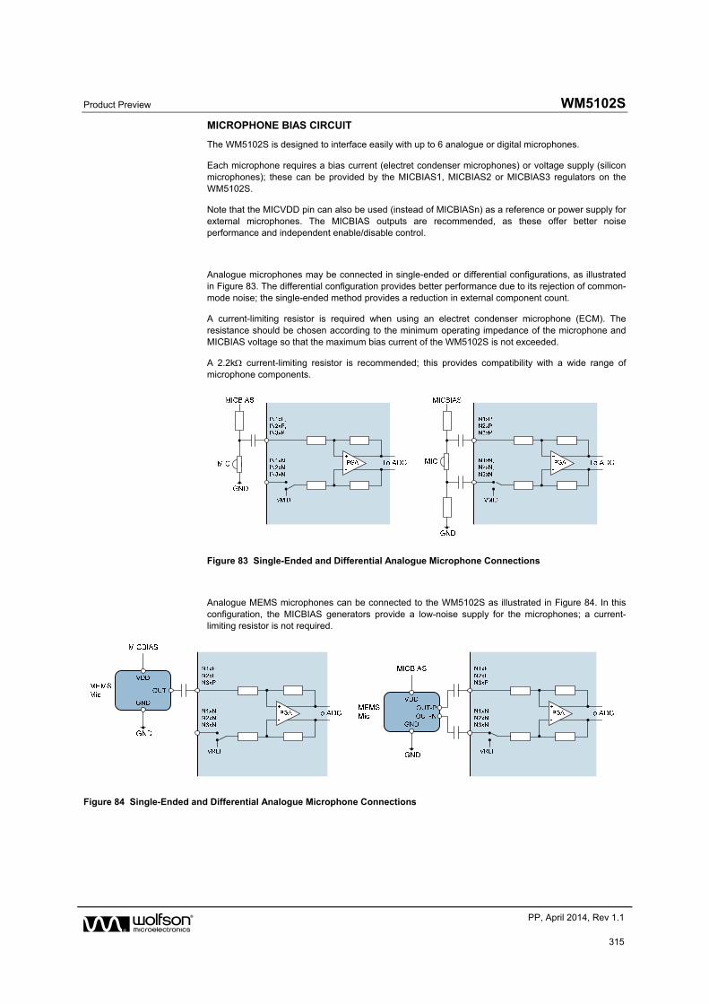
Product Preview WM5102S
w PP, April 2014, Rev 1.1
315
MICROPHONE BIAS CIRCUIT
The WM5102S is designed to interface easily with up to 6 analogue or digital microphones.
Each microphone requires a bias current (electret condenser microphones) or voltage supply (silicon microphones); these can be provided by the MICBIAS1, MICBIAS2 or MICBIAS3 regulators on the WM5102S.
Note that the MICVDD pin can also be used (instead of MICBIASn) as a reference or power supply for external microphones. The MICBIAS outputs are recommended, as these offer better noise performance and independent enable/disable control.
Analogue microphones may be connected in single-ended or differential configurations, as illustrated in Figure 83. The differential configuration provides better performance due to its rejection of common-mode noise; the single-ended method provides a reduction in external component count.
A current-limiting resistor is required when using an electret condenser microphone (ECM). The resistance should be chosen according to the minimum operating impedance of the microphone and MICBIAS voltage so that the maximum bias current of the WM5102S is not exceeded.
A 2.2k current-limiting resistor is recommended; this provides compatibility with a wide range of microphone components.
Figure 83 Single-Ended and Differential Analogue Microphone Connections
Analogue MEMS microphones can be connected to the WM5102S as illustrated in Figure 84. In this configuration, the MICBIAS generators provide a low-noise supply for the microphones; a current-limiting resistor is not required.
Figure 84 Single-Ended and Differential Analogue Microphone Connections
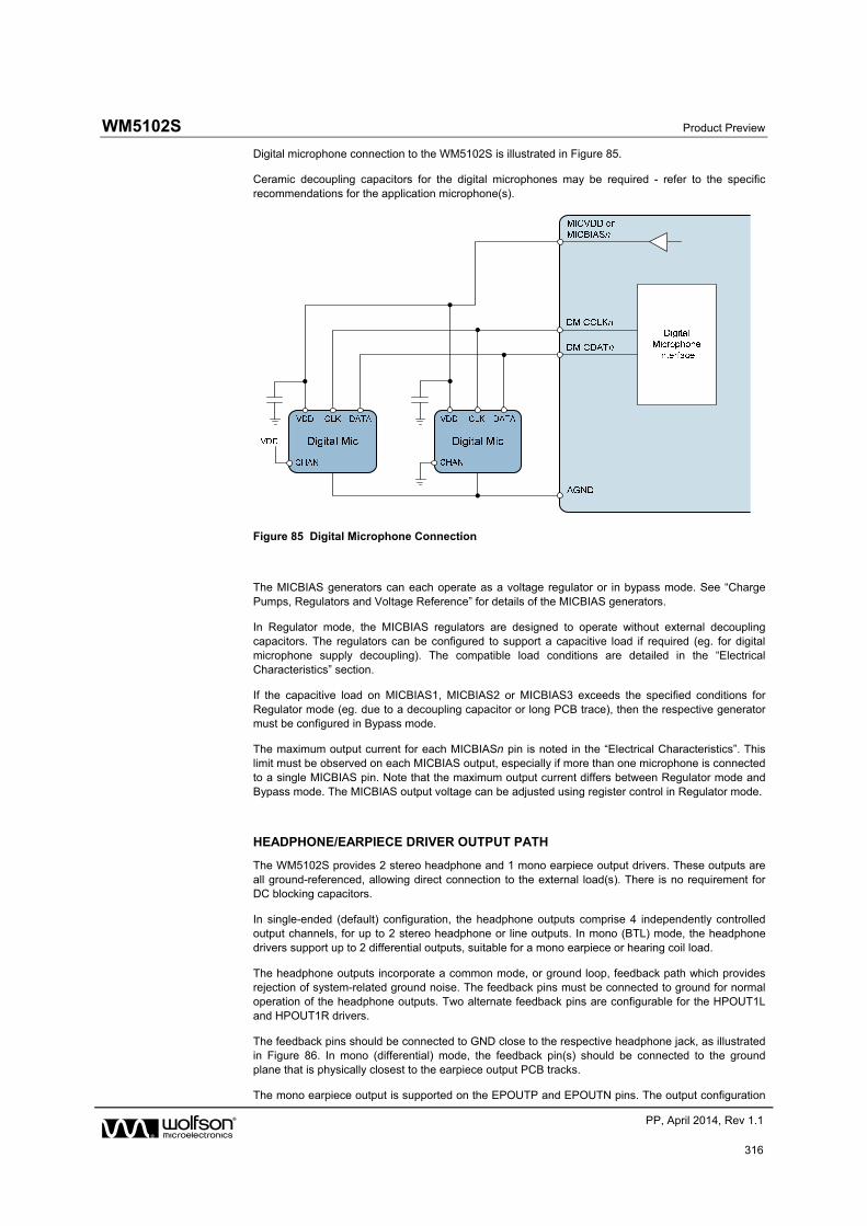
WM5102S Product Preview
w PP, April 2014, Rev 1.1
316
Digital microphone connection to the WM5102S is illustrated in Figure 85.
Ceramic decoupling capacitors for the digital microphones may be required - refer to the specific recommendations for the application microphone(s).
Figure 85 Digital Microphone Connection
The MICBIAS generators can each operate as a voltage regulator or in bypass mode. See “Charge Pumps, Regulators and Voltage Reference” for details of the MICBIAS generators.
In Regulator mode, the MICBIAS regulators are designed to operate without external decoupling capacitors. The regulators can be configured to support a capacitive load if required (eg. for digital microphone supply decoupling). The compatible load conditions are detailed in the “Electrical Characteristics” section.
If the capacitive load on MICBIAS1, MICBIAS2 or MICBIAS3 exceeds the specified conditions for Regulator mode (eg. due to a decoupling capacitor or long PCB trace), then the respective generator must be configured in Bypass mode.
The maximum output current for each MICBIASn pin is noted in the “Electrical Characteristics”. This limit must be observed on each MICBIAS output, especially if more than one microphone is connected to a single MICBIAS pin. Note that the maximum output current differs between Regulator mode and Bypass mode. The MICBIAS output voltage can be adjusted using register control in Regulator mode.
HEADPHONE/EARPIECE DRIVER OUTPUT PATH
The WM5102S provides 2 stereo headphone and 1 mono earpiece output drivers. These outputs are all ground-referenced, allowing direct connection to the external load(s). There is no requirement for DC blocking capacitors.
In single-ended (default) configuration, the headphone outputs comprise 4 independently controlled output channels, for up to 2 stereo headphone or line outputs. In mono (BTL) mode, the headphone drivers support up to 2 differential outputs, suitable for a mono earpiece or hearing coil load.
The headphone outputs incorporate a common mode, or ground loop, feedback path which provides rejection of system-related ground noise. The feedback pins must be connected to ground for normal operation of the headphone outputs. Two alternate feedback pins are configurable for the HPOUT1L and HPOUT1R drivers.
The feedback pins should be connected to GND close to the respective headphone jack, as illustrated in Figure 86. In mono (differential) mode, the feedback pin(s) should be connected to the ground plane that is physically closest to the earpiece output PCB tracks.
The mono earpiece output is supported on the EPOUTP and EPOUTN pins. The output configuration
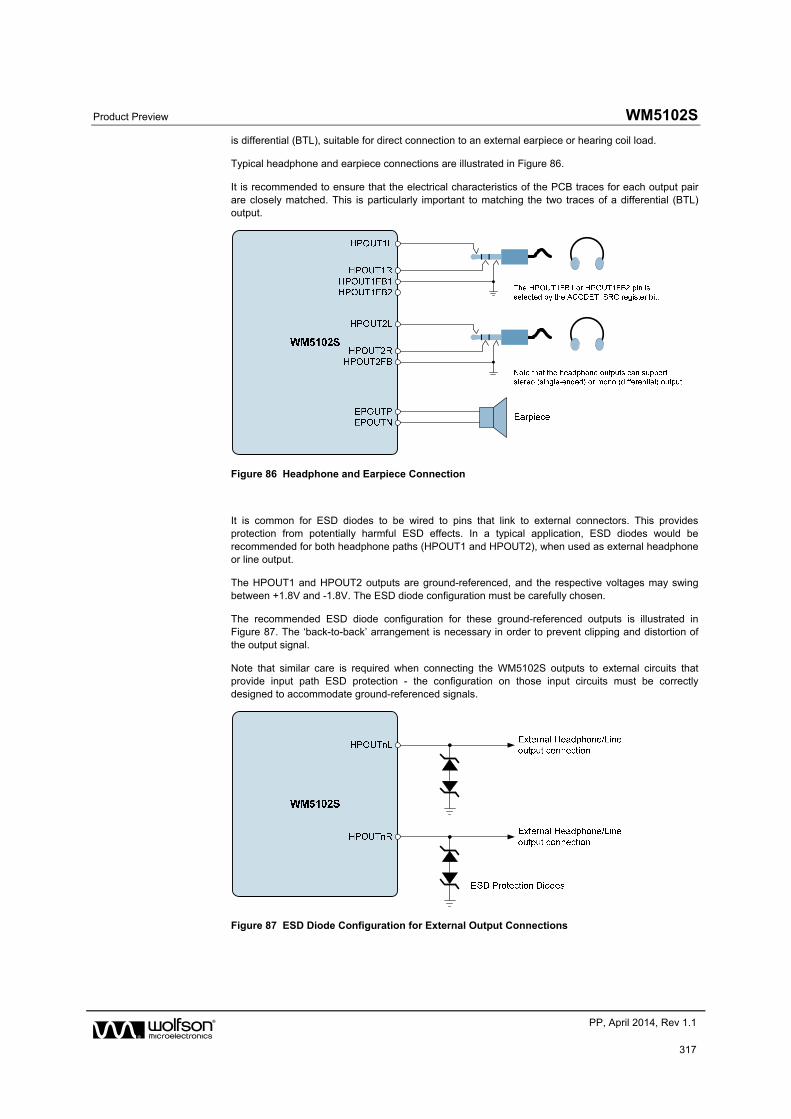
Product Preview WM5102S
w PP, April 2014, Rev 1.1
317
is differential (BTL), suitable for direct connection to an external earpiece or hearing coil load.
Typical headphone and earpiece connections are illustrated in Figure 86.
It is recommended to ensure that the electrical characteristics of the PCB traces for each output pair are closely matched. This is particularly important to matching the two traces of a differential (BTL) output.
Figure 86 Headphone and Earpiece Connection
It is common for ESD diodes to be wired to pins that link to external connectors. This provides protection from potentially harmful ESD effects. In a typical application, ESD diodes would be recommended for both headphone paths (HPOUT1 and HPOUT2), when used as external headphone or line output.
The HPOUT1 and HPOUT2 outputs are ground-referenced, and the respective voltages may swing between +1.8V and -1.8V. The ESD diode configuration must be carefully chosen.
The recommended ESD diode configuration for these ground-referenced outputs is illustrated in Figure 87. The ‘back-to-back’ arrangement is necessary in order to prevent clipping and distortion of the output signal.
Note that similar care is required when connecting the WM5102S outputs to external circuits that provide input path ESD protection - the configuration on those input circuits must be correctly designed to accommodate ground-referenced signals.
Figure 87 ESD Diode Configuration for External Output Connections
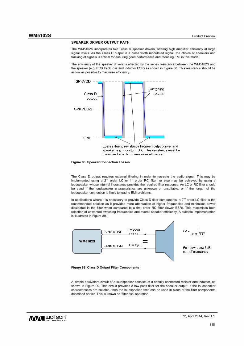
WM5102S Product Preview
w PP, April 2014, Rev 1.1
318
SPEAKER DRIVER OUTPUT PATH
The WM5102S incorporates two Class D speaker drivers, offering high amplifier efficiency at large signal levels. As the Class D output is a pulse width modulated signal, the choice of speakers and tracking of signals is critical for ensuring good performance and reducing EMI in this mode.
The efficiency of the speaker drivers is affected by the series resistance between the WM5102S and the speaker (e.g. PCB track loss and inductor ESR) as shown in Figure 88. This resistance should be as low as possible to maximise efficiency.
Figure 88 Speaker Connection Losses
The Class D output requires external filtering in order to recreate the audio signal. This may be implemented using a 2nd order LC or 1st order RC filter, or else may be achieved by using a loudspeaker whose internal inductance provides the required filter response. An LC or RC filter should be used if the loudspeaker characteristics are unknown or unsuitable, or if the length of the loudspeaker connection is likely to lead to EMI problems.
In applications where it is necessary to provide Class D filter components, a 2nd order LC filter is the recommended solution as it provides more attenuation at higher frequencies and minimises power dissipated in the filter when compared to a first order RC filter (lower ESR). This maximises both rejection of unwanted switching frequencies and overall speaker efficiency. A suitable implementation is illustrated in Figure 89.
Figure 89 Class D Output Filter Components
A simple equivalent circuit of a loudspeaker consists of a serially connected resistor and inductor, as shown in Figure 90. This circuit provides a low pass filter for the speaker output. If the loudspeaker characteristics are suitable, then the loudspeaker itself can be used in place of the filter components described earlier. This is known as ‘filterless’ operation.
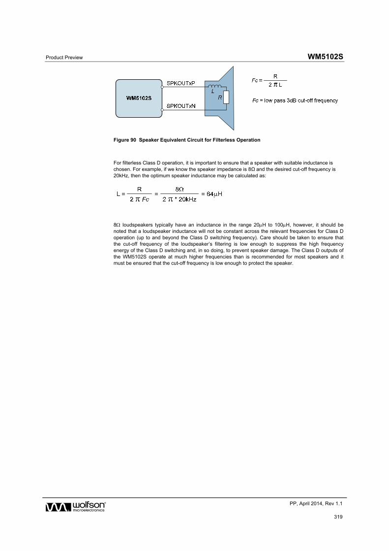
Product Preview WM5102S
w PP, April 2014, Rev 1.1
319
Figure 90 Speaker Equivalent Circuit for Filterless Operation
For filterless Class D operation, it is important to ensure that a speaker with suitable inductance is chosen. For example, if we know the speaker impedance is 8Ω and the desired cut-off frequency is 20kHz, then the optimum speaker inductance may be calculated as:
8 loudspeakers typically have an inductance in the range 20H to 100H, however, it should be noted that a loudspeaker inductance will not be constant across the relevant frequencies for Class D operation (up to and beyond the Class D switching frequency). Care should be taken to ensure that the cut-off frequency of the loudspeaker’s filtering is low enough to suppress the high frequency energy of the Class D switching and, in so doing, to prevent speaker damage. The Class D outputs of the WM5102S operate at much higher frequencies than is recommended for most speakers and it must be ensured that the cut-off frequency is low enough to protect the speaker.
WM5102S Product Preview
w PP, April 2014, Rev 1.1
320
POWER SUPPLY / REFERENCE DECOUPLING
Electrical coupling exists particularly in digital logic systems where switching in one sub-system causes fluctuations on the power supply. This effect occurs because the inductance of the power supply acts in opposition to the changes in current flow that are caused by the logic switching. The resultant variations (‘spikes’) in the power supply voltage can cause malfunctions and unintentional behavior in other components. A decoupling (‘bypass’) capacitor can be used as an energy storage component which will provide power to the decoupled circuit for the duration of these power supply variations, protecting it from malfunctions that could otherwise arise.
Coupling also occurs in a lower frequency form when ripple is present on the power supply rail caused by changes in the load current or by limitations of the power supply regulation method. In audio components such as the WM5102S, these variations can alter the performance of the signal path, leading to degradation in signal quality. A decoupling capacitor can be used to filter these effects, by presenting the ripple voltage with a low impedance path that does not affect the circuit to be decoupled.
These coupling effects are addressed by placing a capacitor between the supply rail and the corresponding ground reference. In the case of systems comprising multiple power supply rails, decoupling should be provided on each rail.
The recommended power supply and voltage reference decoupling capacitors for WM5102S are detailed below in Table 128.
POWER SUPPLY DECOUPLING CAPACITOR
LDOVDD, DBVDD1, DBVDD2, DBVDD3, AVDD 0.1F ceramic (see Note)
CPVDD 4.7F ceramic
MICVDD 4.7F ceramic
DCVDD 4.7F ceramic
SPKVDDL, SPKVDDR 4.7F ceramic
VREFC 1.0F ceramic
Table 128 Power Supply Decoupling Capacitors
Note: 0.1F is required with 4.7F a guide to the total required power rail capacitance.
All decoupling capacitors should be placed as close as possible to the WM5102S device. The connection between AGND, the AVDD decoupling capacitor and the main system ground should be made at a single point as close as possible to the AGND balls of the WM5102S.
Due to the wide tolerance of many types of ceramic capacitors, care must be taken to ensure that the selected components provide the required capacitance across the required temperature and voltage ranges in the intended application. For most application the use of ceramic capacitors with capacitor dielectric X5R is recommended.

Product Preview WM5102S
w PP, April 2014, Rev 1.1
321
CHARGE PUMP COMPONENTS
The WM5102S incorporates two Charge Pump circuits, identified as CP1 and CP2.
CP1 generates the CP1VOUTP and CP1VOUTN supply rails for the ground-referenced headphone drivers; CP2 generates the CP2VOUT supply rail for the microphone bias (MICBIAS) regulators.
Decoupling capacitors are required on each of the Charge Pump outputs. A fly-back capacitor is also required for each Charge Pump.
The recommended Charge Pump capacitors for WM5102S are detailed below in Table 129.
DESCRIPTION CAPACITOR
CP1VOUTP decoupling Required capacitance is 2.0F at 2V. Suitable component typically 4.7F.
CP1VOUTN decoupling Required capacitance is 2.0F at 2V. Suitable component typically 4.7F.
CP1 fly-back (connect between CP1CA and CP1CB)
Required capacitance is 1.0F at 2V. Suitable component typically 2.2F.
CP2VOUT decoupling Required capacitance is 1.0F at 3.6V. Suitable component typically 4.7F.
CP2 fly-back (connect between CP2CA and CP2CB)
Required capacitance is 220nF at 2V. Suitable component typically 470nF.
Table 129 Charge Pump External Capacitors
Ceramic capacitors are recommended for these Charge Pump requirements. Note that, due to the wide tolerance of many types of ceramic capacitors, care must be taken to ensure that the selected components provide the required capacitance across the required temperature and voltage ranges in the intended application. Ceramic capacitors with X5R dielectric are recommended.
The positioning of the Charge Pump capacitors is important, particularly the fly-back capacitors. These capacitors should be placed as close as possible to the WM5102S. The component choice and positioning of the CP1 components are more critical than those of CP2, due to the higher output power requirements of CP1.
EXTERNAL ACCESSORY DETECTION COMPONENTS
The external accessory detection circuit measures jack insertion using the JACKDET pin. The insertion switch status is detected using an internal pull-up resistor circuit on the JACKDET pin.
Microphone detection and key-button press detection is supported using the MICDETn pins. The applicable pin should be connected to one of the MICBIASn outputs, via a 2.2k current-limiting resistor, as described in the “Microphone Bias Circuit” section. Note that, when using the External Accessory Detection function, the MICBIASn resistor must be 2.2k +/-2%.
A recommended circuit configuration, including headphone output on HPOUT1 and microphone connections, is shown in Figure 91. See “Analogue Input Paths” for details of the DC-blocking microphone input capacitor selection.
The recommended external components and connections for microphone / push-button detection are illustrated in Figure 92.
Note that, when using the Microphone Detect circuit, it is recommended to use one of the Right channel analogue microphone input paths, to ensure best immunity to electrical transients arising from the external accessory.
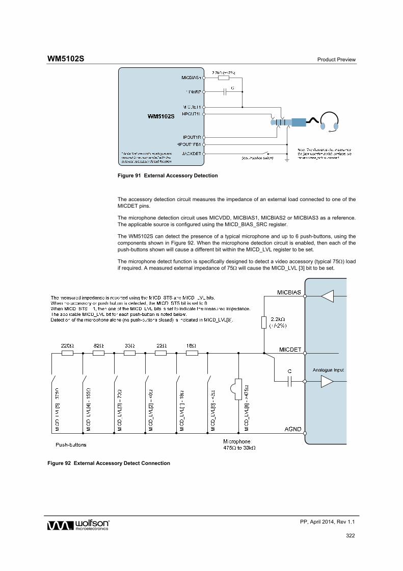
WM5102S Product Preview
w PP, April 2014, Rev 1.1
322
Figure 91 External Accessory Detection
The accessory detection circuit measures the impedance of an external load connected to one of the MICDET pins.
The microphone detection circuit uses MICVDD, MICBIAS1, MICBIAS2 or MICBIAS3 as a reference. The applicable source is configured using the MICD_BIAS_SRC register.
The WM5102S can detect the presence of a typical microphone and up to 6 push-buttons, using the components shown in Figure 92. When the microphone detection circuit is enabled, then each of the push-buttons shown will cause a different bit within the MICD_LVL register to be set.
The microphone detect function is specifically designed to detect a video accessory (typical 75) load if required. A measured external impedance of 75 will cause the MICD_LVL [3] bit to be set.
Figure 92 External Accessory Detect Connection
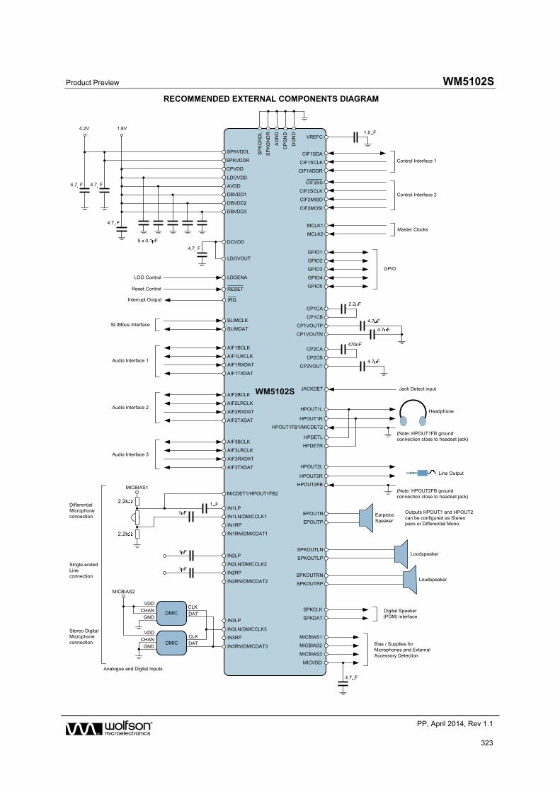
Product Preview WM5102S
w PP, April 2014, Rev 1.1
323
RECOMMENDED EXTERNAL COMPONENTS DIAGRAM
WM5102S
AVDD
CPVDD
CP1CA
CP1VOUTN
CP1VOUTP
CP1CB
2.2 F
4.7 F
4.7 F
4.7 F
4.7 F
4.2V 1.8V
LDOVOUT
SPKVDDL
4.7 F
DBVDD1
DBVDD2
DBVDD3
5 x 0.1 F
Analogue and Digital Inputs
Outputs HPOUT1 and HPOUT2 can be configured as Stereo pairs or Differential Mono.
SPKVDDR
LDOVDD
DCVDD4.7 F
VREFC1.0 F
GPIOGPIO3
GPIO4
GPIO5
Digital Speaker (PDM) interface
SPKCLK
SPKDAT
HPOUT1R
HPOUT1FB1/MICDET2
HPOUT1L Headphone
(Note: HPOUT1FB ground connection close to headset jack)
CIF1SDA
CIF1SCLK Control Interface 1
CIF1ADDR
MCLK1
MCLK2Master Clocks
AIF1RXDAT
AIF1LRCLK
AIF1BCLK
AIF1TXDAT
Audio Interface 1
AIF2RXDAT
AIF2LRCLK
AIF2BCLK
AIF2TXDAT
Audio Interface 2
Audio Interface 3AIF3RXDAT
AIF3LRCLK
AIF3BCLK
AIF3TXDAT
LDOENALDO Control
RESETReset Control
CP2CA
CP2VOUT
CP2CB
470nF
4.7 F
SP
KG
ND
R
DG
ND
CP
GN
D
AG
ND
SP
KG
ND
L
HPOUT2R
HPOUT2FB
HPOUT2L
(Note: HPOUT2FB ground connection close to headset jack)
EPOUTN
EPOUTP
EarpieceSpeaker
SPKOUTLN
SPKOUTRP
SPKOUTRN
SPKOUTLPLoudspeaker
Loudspeaker
HPDETL
HPDETR
MICBIAS2
MICBIAS1
MICBIAS3
MICVDD
Bias / Supplies for Microphones and External Accessory Detection
Differential Microphoneconnection
Single-ended Line connection
Stereo Digital Microphone connection
4.7 F
GPIO1
GPIO2
IRQInterrupt Output
SLIMDAT
SLIMCLKSLIMbus Interface
CIF2SS
CIF2SCLK
CIF2MISO
CIF2MOSI
Control Interface 2
JACKDET Jack Detect input
IN2LP
IN2LN/DMICCLK2
IN2RP
IN2RN/DMICDAT2
1 F
1 F
IN3LN/DMICCLK3
IN3LP
IN3RN/DMICDAT3
IN3RP
DMICCLK
DAT
CLK
DAT
VDD
CHAN
MICBIAS2
DMIC
GND
VDD
CHAN
GND
IN1LP
IN1RN/DMICDAT1
IN1RP
IN1LN/DMICCLK11 F
MICDET1/HPOUT1FB2
1 F2.2k
2.2k
MICBIAS1
Line Output
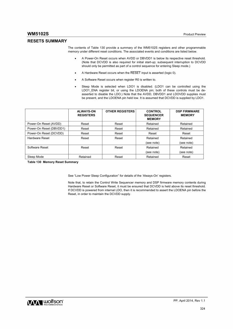
WM5102S Product Preview
w PP, April 2014, Rev 1.1
324
RESETS SUMMARY
The contents of Table 130 provide a summary of the WM5102S registers and other programmable memory under different reset conditions. The associated events and conditions are listed below.
A Power-On Reset occurs when AVDD or DBVDD1 is below its respective reset threshold. (Note that DCVDD is also required for initial start-up; subsequent interruption to DCVDD should only be permitted as part of a control sequence for entering Sleep mode.)
A Hardware Reset occurs when the RESET¯¯¯¯¯¯ input is asserted (logic 0).
A Software Reset occurs when register R0 is written to.
Sleep Mode is selected when LDO1 is disabled. (LDO1 can be controlled using the LDO1_ENA register bit, or using the LDOENA pin; both of these controls must be de-asserted to disable the LDO.) Note that the AVDD, DBVDD1 and LDOVDD supplies must be present, and the LDOENA pin held low. It is assumed that DCVDD is supplied by LDO1.
ALWAYS-ON REGISTERS
OTHER REGISTERS CONTROL SEQUENCER
MEMORY
DSP FIRMWARE MEMORY
Power-On Reset (AVDD) Reset Reset Retained Retained
Power-On Reset (DBVDD1) Reset Reset Retained Retained
Power-On Reset (DCVDD) Reset Reset Reset Reset
Hardware Reset Reset Reset Retained
(see note)
Retained
(see note)
Software Reset Reset Reset Retained
(see note)
Retained
(see note)
Sleep Mode Retained Reset Retained Reset
Table 130 Memory Reset Summary
See “Low Power Sleep Configuration” for details of the ‘Always-On’ registers.
Note that, to retain the Control Write Sequencer memory and DSP firmware memory contents during Hardware Reset or Software Reset, it must be ensured that DCVDD is held above its reset threshold. If DCVDD is powered from internal LDO, then it is recommended to assert the LDOENA pin before the Reset, in order to maintain the DCVDD supply.
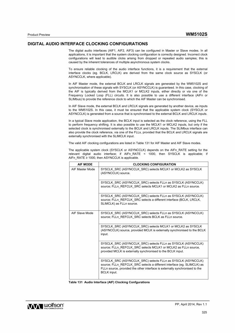
Product Preview WM5102S
w PP, April 2014, Rev 1.1
325
DIGITAL AUDIO INTERFACE CLOCKING CONFIGURATIONS
The digital audio interfaces (AIF1, AIF2, AIF3) can be configured in Master or Slave modes. In all applications, it is important that the system clocking configuration is correctly designed. Incorrect clock configurations will lead to audible clicks arising from dropped or repeated audio samples; this is caused by the inherent tolerances of multiple asynchronous system clocks.
To ensure reliable clocking of the audio interface functions, it is a requirement that the external interface clocks (eg. BCLK, LRCLK) are derived from the same clock source as SYSCLK (or ASYNCCLK, where applicable).
In AIF Master mode, the external BCLK and LRCLK signals are generated by the WM5102S and synchronisation of these signals with SYSCLK (or ASYNCCLK) is guaranteed. In this case, clocking of the AIF is typically derived from the MCLK1 or MCLK2 inputs, either directly or via one of the Frequency Locked Loop (FLL) circuits. It is also possible to use a different interface (AIFn or SLIMbus) to provide the reference clock to which the AIF Master can be synchronised.
In AIF Slave mode, the external BCLK and LRCLK signals are generated by another device, as inputs to the WM5102S. In this case, it must be ensured that the applicable system clock (SYSCLK or ASYNCCLK) is generated from a source that is synchronised to the external BCLK and LRCLK inputs.
In a typical Slave mode application, the BCLK input is selected as the clock reference, using the FLL to perform frequency shifting. It is also possible to use the MCLK1 or MCLK2 inputs, but only if the selected clock is synchronised externally to the BCLK and LRCLK inputs. The SLIMbus interface can also provide the clock reference, via one of the FLLs, provided that the BCLK and LRCLK signals are externally synchronised with the SLIMCLK input.
The valid AIF clocking configurations are listed in Table 131 for AIF Master and AIF Slave modes.
The applicable system clock (SYSCLK or ASYNCCLK) depends on the AIFn_RATE setting for the relevant digital audio interface; if AIFn_RATE < 1000, then SYSCLK is applicable; if AIFn_RATE ≥ 1000, then ASYNCCLK is applicable.
AIF MODE CLOCKING CONFIGURATION
AIF Master Mode SYSCLK_SRC (ASYNCCLK_SRC) selects MCLK1 or MCLK2 as SYSCLK (ASYNCCLK) source.
SYSCLK_SRC (ASYNCCLK_SRC) selects FLLn as SYSCLK (ASYNCCLK) source; FLLn_REFCLK_SRC selects MCLK1 or MCLK2 as FLLn source.
SYSCLK_SRC (ASYNCCLK_SRC) selects FLLn as SYSCLK (ASYNCCLK) source; FLLn_REFCLK_SRC selects a different interface (BCLK, LRCLK, SLIMCLK) as FLLn source.
AIF Slave Mode SYSCLK_SRC (ASYNCCLK_SRC) selects FLLn as SYSCLK (ASYNCCLK) source; FLLn_REFCLK_SRC selects BCLK as FLLn source.
SYSCLK_SRC (ASYNCCLK_SRC) selects MCLK1 or MCLK2 as SYSCLK (ASYNCCLK) source, provided MCLK is externally synchronised to the BCLK input.
SYSCLK_SRC (ASYNCCLK_SRC) selects FLLn as SYSCLK (ASYNCCLK) source; FLLn_REFCLK_SRC selects MCLK1 or MCLK2 as FLLn source, provided MCLK is externally synchronised to the BCLK input.
SYSCLK_SRC (ASYNCCLK_SRC) selects FLLn as SYSCLK (ASYNCCLK) source; FLLn_REFCLK_SRC selects a different interface (eg. SLIMCLK) as FLLn source, provided the other interface is externally synchronised to the BCLK input.
Table 131 Audio Interface (AIF) Clocking Confgurations

WM5102S Product Preview
w PP, April 2014, Rev 1.1
326
In each case, the SYSCLK (ASYNCCLK) frequency must be a valid ratio to the LRCLK frequency; the supported clocking rates are defined by the SYSCLK_FREQ (ASYNC_CLK_FREQ) and SAMPLE_RATE_n (ASYNC_SAMPLE_RATE_n) registers.
The valid AIF clocking configurations are illustrated in Figure 93 to Figure 99 below. Note that, where MCLK1 is illustrated as the clock source, it is equally possible to select MCLK2 as the clock source. Similarly, in cases where FLL1 is illustrated, it is equally possible to select FLL2.
Figure 93 AIF Master Mode, using MCLK as Reference
Figure 94 AIF Master Mode, using MCLK and FLL as Reference
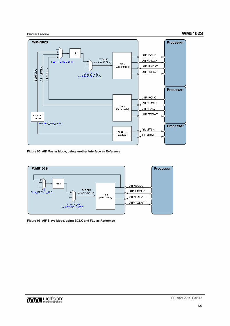
Product Preview WM5102S
w PP, April 2014, Rev 1.1
327
Figure 95 AIF Master Mode, using another Interface as Reference
Figure 96 AIF Slave Mode, using BCLK and FLL as Reference
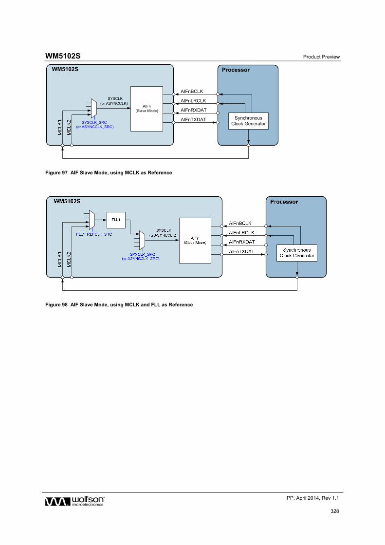
WM5102S Product Preview
w PP, April 2014, Rev 1.1
328
AIFn(Slave Mode)
WM5102S Processor
AIFnBCLK
AIFnLRCLK
AIFnRXDAT
AIFnTXDAT
SYSCLK(or ASYNCCLK)
SYSCLK_SRC(or ASYNCCLK_SRC)
Synchronous Clock Generator
Figure 97 AIF Slave Mode, using MCLK as Reference
Figure 98 AIF Slave Mode, using MCLK and FLL as Reference
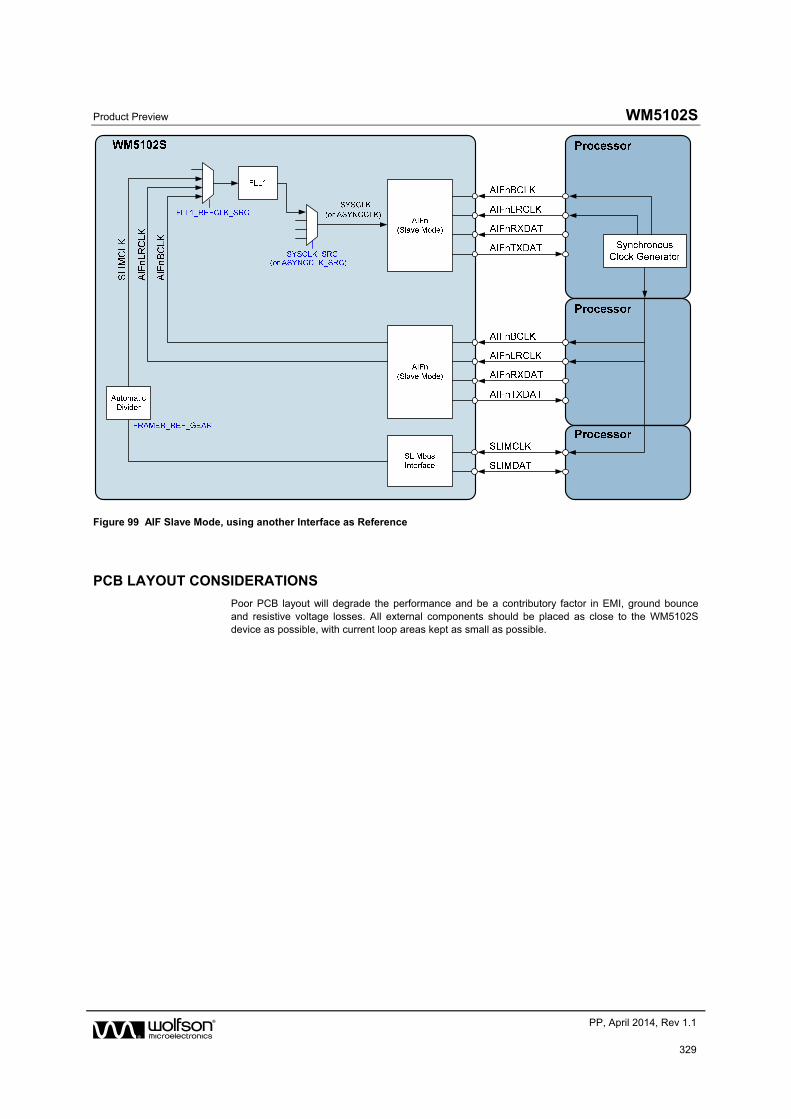
Product Preview WM5102S
w PP, April 2014, Rev 1.1
329
Figure 99 AIF Slave Mode, using another Interface as Reference
PCB LAYOUT CONSIDERATIONS
Poor PCB layout will degrade the performance and be a contributory factor in EMI, ground bounce and resistive voltage losses. All external components should be placed as close to the WM5102S device as possible, with current loop areas kept as small as possible.
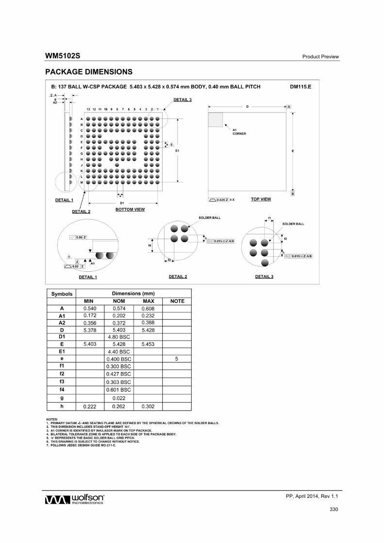
WM5102S Product Preview
w PP, April 2014, Rev 1.1
330
PACKAGE DIMENSIONS
Product Preview WM5102S
w PP, April 2014, Rev 1.1
331
IMPORTANT NOTICE
Wolfson Microelectronics plc (“Wolfson”) products and services are sold subject to Wolfson’s terms and conditions of sale, delivery and payment supplied at the time of order acknowledgement.
Wolfson warrants performance of its products to the specifications in effect at the date of shipment. Wolfson reserves the right to make changes to its products and specifications or to discontinue any product or service without notice. Customers should therefore obtain the latest version of relevant information from Wolfson to verify that the information is current.
Testing and other quality control techniques are utilised to the extent Wolfson deems necessary to support its warranty. Specific testing of all parameters of each device is not necessarily performed unless required by law or regulation.
In order to minimise risks associated with customer applications, the customer must use adequate design and operating safeguards to minimise inherent or procedural hazards. Wolfson is not liable for applications assistance or customer product design. The customer is solely responsible for its selection and use of Wolfson products. Wolfson is not liable for such selection or use nor for use of any circuitry other than circuitry entirely embodied in a Wolfson product.
Wolfson’s products are not intended for use in life support systems, appliances, nuclear systems or systems where malfunction can reasonably be expected to result in personal injury, death or severe property or environmental damage. Any use of products by the customer for such purposes is at the customer’s own risk.
Wolfson does not grant any licence (express or implied) under any patent right, copyright, mask work right or other intellectual property right of Wolfson covering or relating to any combination, machine, or process in which its products or services might be or are used. Any provision or publication of any third party’s products or services does not constitute Wolfson’s approval, licence, warranty or endorsement thereof. Any third party trade marks contained in this document belong to the respective third party owner.
Reproduction of information from Wolfson datasheets is permissible only if reproduction is without alteration and is accompanied by all associated copyright, proprietary and other notices (including this notice) and conditions. Wolfson is not liable for any unauthorised alteration of such information or for any reliance placed thereon.
Any representations made, warranties given, and/or liabilities accepted by any person which differ from those contained in this datasheet or in Wolfson’s standard terms and conditions of sale, delivery and payment are made, given and/or accepted at that person’s own risk. Wolfson is not liable for any such representations, warranties or liabilities or for any reliance placed thereon by any person.
ADDRESS:
Wolfson Microelectronics plc
26 Westfield Road
Edinburgh
EH11 2QB
United Kingdom
Tel :: +44 (0)131 272 7000
Fax :: +44 (0)131 272 7001
Email :: [email protected]
WM5102S Product Preview
w PP, April 2014, Rev 1.1
332
REVISION HISTORY
DATE REV DESCRIPTION OF CHANGES PAGE CHANGED BY
07/02/14 1.0 Initial version PH
10/04/14 1.1 Block Diagram updated 2 PH


![2-in, 4-out CODEC with DSP FunctionsAK4753] MS1311-E-04 2013/04 - 1 - GENERAL DESCRIPTION The AK4753 is a two input, four output audio CODEC with integrated digital signal processing](https://img.dokumen.tips/doc/110x75/5add882d7f8b9a9d4d8d4811/2-in-4-out-codec-with-dsp-functions-ak4753-ms1311-e-04-201304-1-general-description.jpg)


![Audio Hub CODEC with Master Hi-Fi DSPw WM5102S Audio Hub CODEC with Master Hi-Fi DSP WOLFSON MICROELECTRONICS plc Product Preview, April 2014, Rev 1.1 [1] This product is protected](https://img.dokumen.tips/doc/110x75/5e858796f50cec40e50051dd/audio-hub-codec-with-master-hi-fi-dsp-w-wm5102s-audio-hub-codec-with-master-hi-fi.jpg)