Embed Size (px)
Citation preview
© M. Shabany, ASIC/FPGA Chip Design
ASIC/FPGA Chip Design
Mahdi Shabany
Department of Electrical Engineering
Sharif University of technology
HDL Coding (Verilog)
© M. Shabany, ASIC/FPGA Chip Design
Outline
ASIC/FPGA Design Flow
Hardware Description Language (HDL)
Verilog
o Introduction
o Language Fundamentals
o Modeling Combinational & Sequential Logic Circuits
o Modeling Finite State Machines
o Verilog Operations
2
© M. Shabany, ASIC/FPGA Chip Design
Outline
ASIC/FPGA Design Flow
Hardware Description Language (HDL)
Verilog
o Introduction
o Language Fundamentals
o Modeling Combinational & Sequential Logic Circuits
o Modeling Finite State Machines
o Verilog Operations
3
© M. Shabany, ASIC/FPGA Chip Design
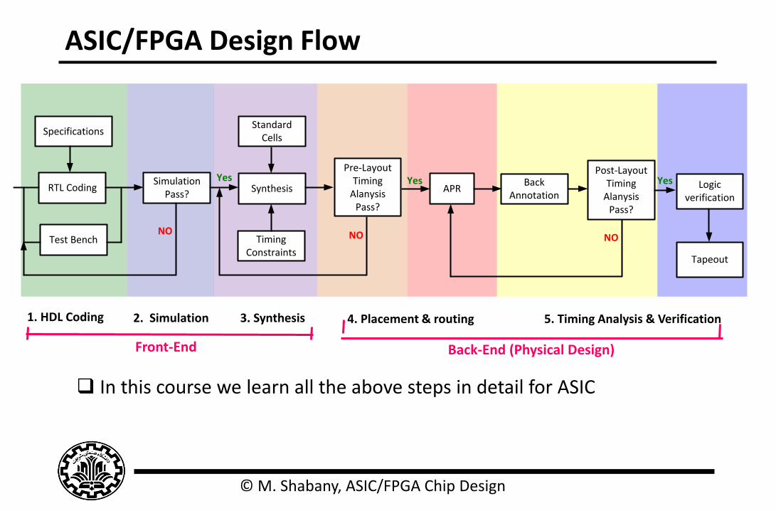
ASIC/FPGA Design Flow
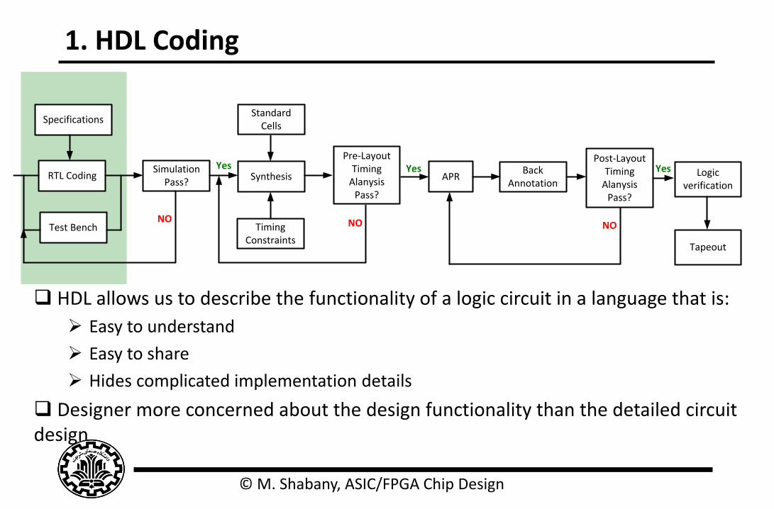
1. HDL Coding
RTL CodingSimulation
Pass?
Test Bench
Specifications
Synthesis
Standard Cells
Timing Constraints
Pre-Layout Timing
AlanysisPass?
APRBack
Annotation
Post-Layout Timing
AlanysisPass?
Logic verification
Tapeout
Yes
NO
Yes
NO
Yes
NO
2. Simulation
3. Synthesis 4. Placement & routing
5. Timing Analysis & Verification
In this course we learn all the above steps in detail for ASIC
Front-End Back-End (Physical Design)
© M. Shabany, ASIC/FPGA Chip Design
1. HDL Coding
RTL CodingSimulation
Pass?
Test Bench
Specifications
Synthesis
Standard Cells
Timing Constraints
Pre-Layout Timing
AlanysisPass?
APRBack
Annotation
Post-Layout Timing
AlanysisPass?
Logic verification
Tapeout
Yes
NO
Yes
NO
Yes
NO
HDL allows us to describe the functionality of a logic circuit in a language that is:
Easy to understand
Easy to share
Hides complicated implementation details
Designer more concerned about the design functionality than the detailed circuit design

© M. Shabany, ASIC/FPGA Chip Design
2. Simulation by Testbenches
RTL CodingSimulation
Pass?
Test Bench
Specifications
Synthesis
Standard Cells
Timing Constraints
Pre-Layout Timing
AlanysisPass?
APRBack
Annotation
Post-Layout Timing
AlanysisPass?
Logic verification
Tapeout
Yes
NO
Yes
NO
Yes
NO
After HDL coding, the code has to be tested using “testbenches” (Verification).
Simulation tools:
Synopsys VCS (Synopsys)
Modelsim (Mentor Graphics)
NCVerilog (Cadence)
© M. Shabany, ASIC/FPGA Chip Design
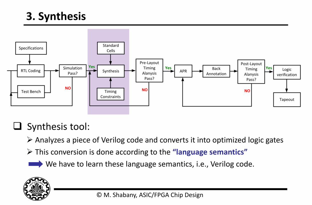
3. Synthesis
RTL CodingSimulation
Pass?
Test Bench
Specifications
Synthesis
Standard Cells
Timing Constraints
Pre-Layout Timing
AlanysisPass?
APRBack
Annotation
Post-Layout Timing
AlanysisPass?
Logic verification
Tapeout
Yes
NO
Yes
NO
Yes
NO
Synthesis tool: Analyzes a piece of Verilog code and converts it into optimized logic gates
This conversion is done according to the “language semantics”
We have to learn these language semantics, i.e., Verilog code.
© M. Shabany, ASIC/FPGA Chip Design
3. Synthesis
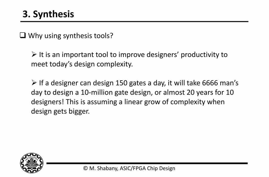
Why using synthesis tools? It is an important tool to improve designers’ productivity to meet today’s design complexity.
If a designer can design 150 gates a day, it will take 6666 man’s day to design a 10-million gate design, or almost 20 years for 10 designers! This is assuming a linear grow of complexity when design gets bigger.
© M. Shabany, ASIC/FPGA Chip Design
3. Synthesis
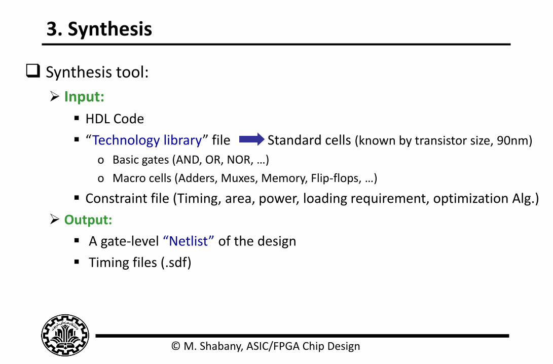
Synthesis tool:
Input:
HDL Code
“Technology library” file Standard cells (known by transistor size, 90nm)
o Basic gates (AND, OR, NOR, …)
o Macro cells (Adders, Muxes, Memory, Flip-flops, …)
Constraint file (Timing, area, power, loading requirement, optimization Alg.)
Output:
A gate-level “Netlist” of the design
Timing files (.sdf)
© M. Shabany, ASIC/FPGA Chip Design
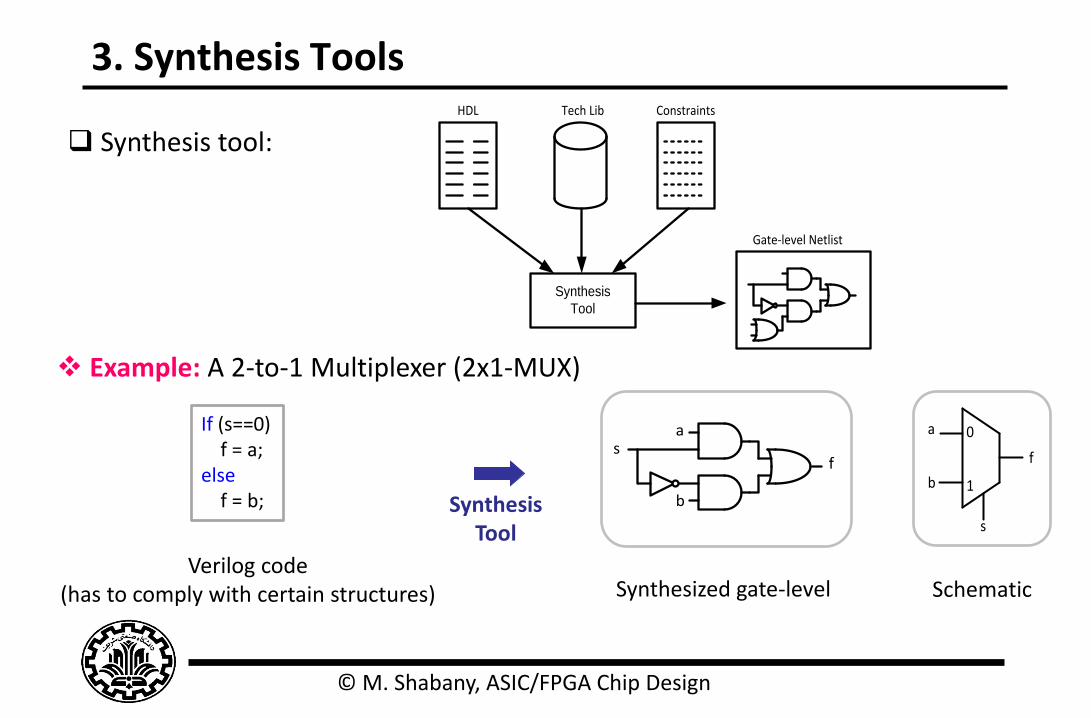
3. Synthesis Tools
Example: A 2-to-1 Multiplexer (2x1-MUX)
If (s==0) f = a; else f = b;
Verilog code (has to comply with certain structures)
a
b
sf
Synthesized gate-level
Synthesis Tool
a
b
s
f
0
1
Schematic
Synthesis
Tool
HDL Tech Lib Constraints
Gate-level Netlist
Synthesis tool:
© M. Shabany, ASIC/FPGA Chip Design
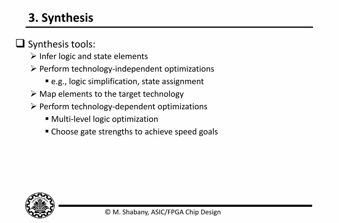
3. Synthesis
Synthesis tools: Infer logic and state elements
Perform technology-independent optimizations
e.g., logic simplification, state assignment
Map elements to the target technology
Perform technology-dependent optimizations
Multi-level logic optimization
Choose gate strengths to achieve speed goals
© M. Shabany, ASIC/FPGA Chip Design
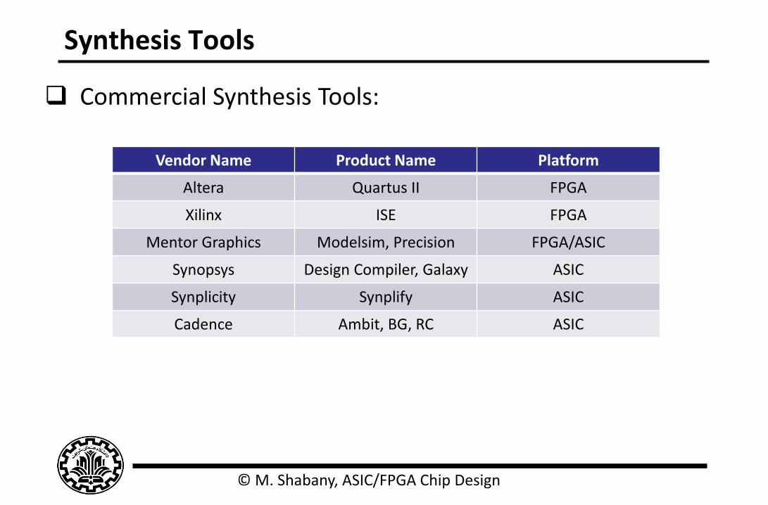
Synthesis Tools
Commercial Synthesis Tools:
Vendor Name Product Name Platform
Altera Quartus II FPGA
Xilinx ISE FPGA
Mentor Graphics Modelsim, Precision FPGA/ASIC
Synopsys Design Compiler, Galaxy ASIC
Synplicity Synplify ASIC
Cadence Ambit, BG, RC ASIC

© M. Shabany, ASIC/FPGA Chip Design
4. Pre-Layout Timing Analysis
Timing analysis across all design corners:
Different voltages and temperatures
Check for setup-time and hold-time violation
Rough estimation as wire delays and RC models are not considered
RTL CodingSimulation
Pass?
Test Bench
Specifications
Synthesis
Standard Cells
Timing Constraints
Pre-Layout Timing
AlanysisPass?
APRBack
Annotation
Post-Layout Timing
AlanysisPass?
Logic verification
Tapeout
Yes
NO
Yes
NO
Yes
NO
© M. Shabany, ASIC/FPGA Chip Design
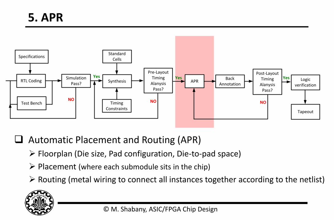
5. APR
Automatic Placement and Routing (APR)
Floorplan (Die size, Pad configuration, Die-to-pad space)
Placement (where each submodule sits in the chip)
Routing (metal wiring to connect all instances together according to the netlist)
RTL CodingSimulation
Pass?
Test Bench
Specifications
Synthesis
Standard Cells
Timing Constraints
Pre-Layout Timing
AlanysisPass?
APRBack
Annotation
Post-Layout Timing
AlanysisPass?
Logic verification
Tapeout
Yes
NO
Yes
NO
Yes
NO

© M. Shabany, ASIC/FPGA Chip Design
6. Back Annotation & Timing Analysis
Back Annotation (Timing Closure)
To estimate the delay after tapeout
Extraction of RC parasitics in the layout netlist interconnect delay
Some paths might now violate (setup-time and hold-time)
Causes increase in the path delay (specially in deep submicron)
RTL CodingSimulation
Pass?
Test Bench
Specifications
Synthesis
Standard Cells
Timing Constraints
Pre-Layout Timing
AlanysisPass?
APRBack
Annotation
Post-Layout Timing
AlanysisPass?
Logic verification
Tapeout
Yes
NO
Yes
NO
Yes
NO
© M. Shabany, ASIC/FPGA Chip Design
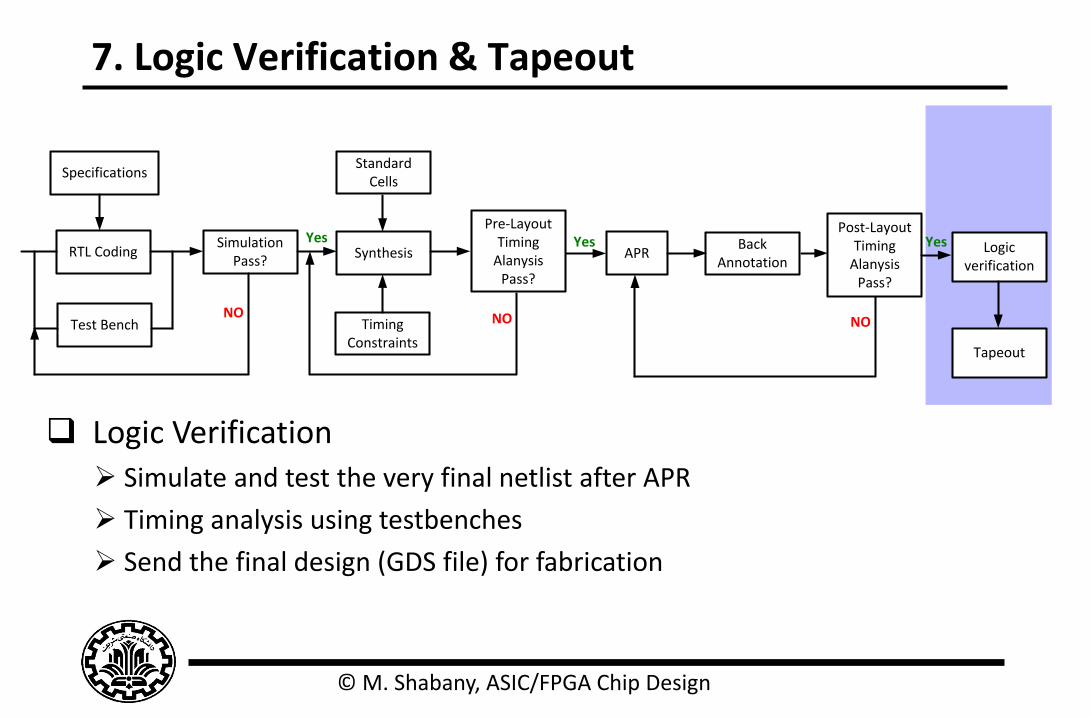
7. Logic Verification & Tapeout
Logic Verification
Simulate and test the very final netlist after APR
Timing analysis using testbenches
Send the final design (GDS file) for fabrication
RTL CodingSimulation
Pass?
Test Bench
Specifications
Synthesis
Standard Cells
Timing Constraints
Pre-Layout Timing
AlanysisPass?
APRBack
Annotation
Post-Layout Timing
AlanysisPass?
Logic verification
Tapeout
Yes
NO
Yes
NO
Yes
NO
© M. Shabany, ASIC/FPGA Chip Design
Outline
ASIC/FPGA Design Flow
Hardware Description Language (HDL)
Verilog
o Introduction
o Language Fundamentals
o Modeling Combinational & Sequential Logic Circuits
o Modeling Finite State Machines
o Verilog Operations
17
© M. Shabany, ASIC/FPGA Chip Design
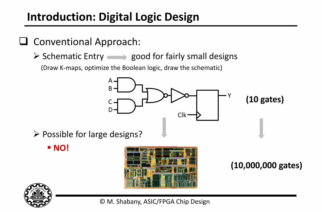
Introduction: Digital Logic Design
Conventional Approach:
Schematic Entry good for fairly small designs (Draw K-maps, optimize the Boolean logic, draw the schematic)
Possible for large designs?
NO!
Y
AB
CD
Clk
(10 gates)
(10,000,000 gates)

© M. Shabany, ASIC/FPGA Chip Design
Introduction: Why HDL?
Schematic entry not feasible for large designs: Time consuming to draw the schematic for millions of gates
Prone to mistakes
Difficult design entry and sharing
Different design entry tools to learn
Tools not compatible (hard to convert the design from one to another)
Not easy to modify
Solution: Describe the design in text Hardware Description Language (HDL)
Just describe the design “behavior” not the detailed gate-level logic
Gate-level logic is generated automatically by a “synthesis” tool

© M. Shabany, ASIC/FPGA Chip Design
Introduction: Why HDL?
Complicated designs can be easily described by HDL
Can be used as the input to the synthesis tool
Supports behavioral and structural descriptions
Supports bit-level descriptions
Detailed design cycle-by-cycle timing is supported
Concurrent cores can be implemented and simultaneously simulated,
which is vital to describe the hardware systems Software programming languages typically have no concept of time. In hardware,
there are delays associated with going from an input to an output.
© M. Shabany, ASIC/FPGA Chip Design
HDL Coding
© M. Shabany, ASIC/FPGA Chip Design
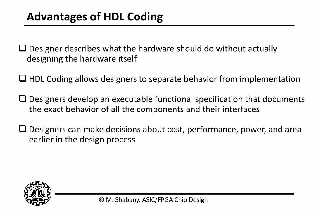
Advantages of HDL Coding
Designer describes what the hardware should do without actually designing the hardware itself HDL Coding allows designers to separate behavior from implementation
Designers develop an executable functional specification that documents the exact behavior of all the components and their interfaces Designers can make decisions about cost, performance, power, and area earlier in the design process
© M. Shabany, ASIC/FPGA Chip Design
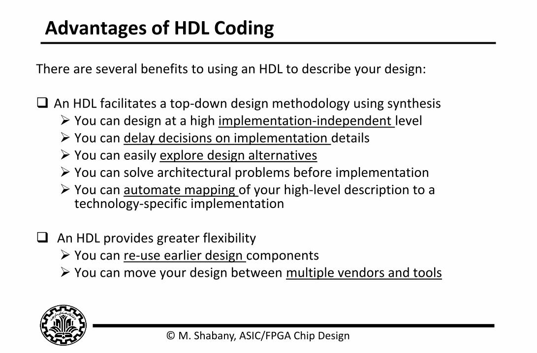
Advantages of HDL Coding
There are several benefits to using an HDL to describe your design:
An HDL facilitates a top-down design methodology using synthesis You can design at a high implementation-independent level You can delay decisions on implementation details You can easily explore design alternatives You can solve architectural problems before implementation You can automate mapping of your high-level description to a
technology-specific implementation
An HDL provides greater flexibility You can re-use earlier design components You can move your design between multiple vendors and tools
© M. Shabany, ASIC/FPGA Chip Design
HDL Coding Goals
1. To simulate digital designs
2. To synthesize digital designs
Some tools can automatically manipulate the design for verification, synthesis, optimization, etc.
Computer Aided Design (CAD) tools
© M. Shabany, ASIC/FPGA Chip Design
HDL is NOT a Software Programming Languae
Software Programming Language
Language which can be translated into machine instructions
and then executed on a computer
Hardware Description Language
Language with syntactic and semantic support for modeling
the temporal behavior and spatial structure of hardware
© M. Shabany, ASIC/FPGA Chip Design
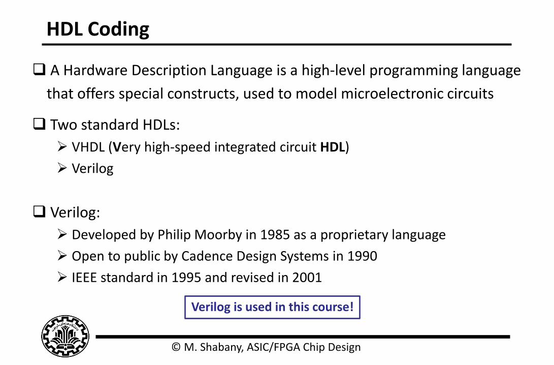
HDL Coding
A Hardware Description Language is a high-level programming language
that offers special constructs, used to model microelectronic circuits
Two standard HDLs:
VHDL (Very high-speed integrated circuit HDL)
Verilog
Verilog:
Developed by Philip Moorby in 1985 as a proprietary language
Open to public by Cadence Design Systems in 1990
IEEE standard in 1995 and revised in 2001
Verilog is used in this course!

© M. Shabany, ASIC/FPGA Chip Design
Verilog or VHDL?
VHDL Verilog Commissioned in 1981 by Department of Defense Created by Gateway Design Automation in 1985
An IEEE standard An IEEE standard
Initially created for ASIC Synthesis Initially an interpreted language for gate-level simulation
Strong support for package management and large designs
No special extensions for large designs
ADA-like verbose syntax, lots of redundancy C-like concise syntax
Design is composed of entities each of which can have multiple architectures
Design is composed of modules which have just one implementation
Gate-level, dataflow, and behavioral modeling. Synthesizable subset.
Gate-level, dataflow, and behavioral modeling. Synthesizable subset.
Harder to learn and use Easy to learn and use

© M. Shabany, ASIC/FPGA Chip Design
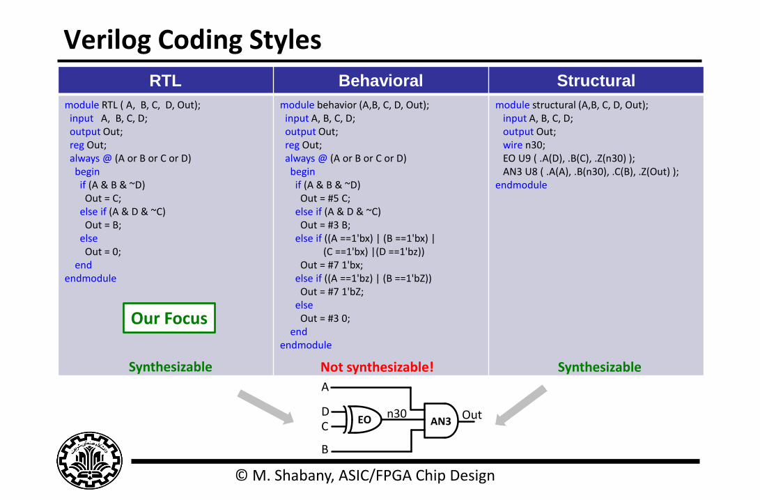
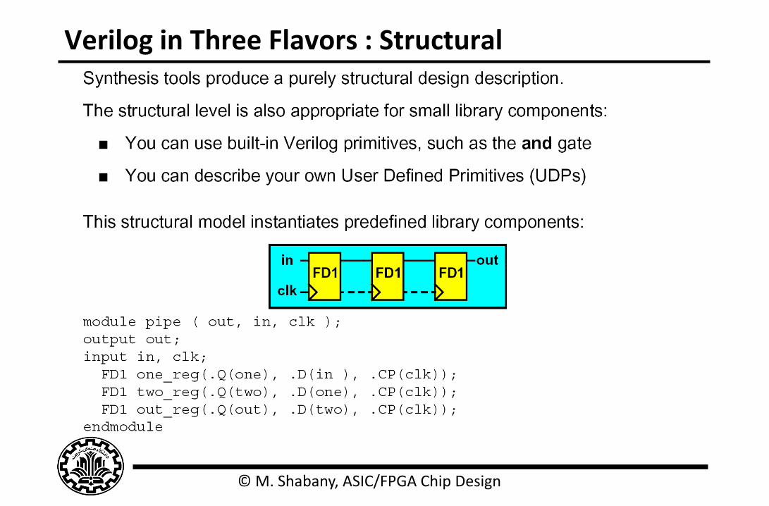
Verilog in Three Flavors
There are three types of Verilog Coding:
Behavioral:
Describes a system by the flow of data between its functional Blocks
Defines signal values when they change
Structural:
Shows detailed design components, nets, and interconnects
Uses technology-specific, low-level components
Used to pass netlist information b/w design tools (e.g., from DC to APR)
RTL (Register Transfer Level):
Describe how data transfers b/w registers and input/outputs
Describes a system by the flow of data and control signals between and
within its functional blocks
Defines signal values with respect to a clock
Focus of this course
Most Descriptive
Least Descriptive
Somehow Descriptive
© M. Shabany, ASIC/FPGA Chip Design
Verilog Coding Styles
RTL Behavioral Structural
module RTL ( A, B, C, D, Out); input A, B, C, D; output Out; reg Out; always @ (A or B or C or D) begin if (A & B & ~D) Out = C; else if (A & D & ~C) Out = B; else Out = 0; end endmodule
module behavior (A,B, C, D, Out); input A, B, C, D; output Out; reg Out; always @ (A or B or C or D) begin if (A & B & ~D) Out = #5 C; else if (A & D & ~C) Out = #3 B; else if ((A ==1'bx) | (B ==1'bx) | (C ==1'bx) |(D ==1'bz)) Out = #7 1'bx; else if ((A ==1'bz) | (B ==1'bZ)) Out = #7 1'bZ; else Out = #3 0; end endmodule
module structural (A,B, C, D, Out); input A, B, C, D; output Out; wire n30; EO U9 ( .A(D), .B(C), .Z(n30) ); AN3 U8 ( .A(A), .B(n30), .C(B), .Z(Out) ); endmodule
Synthesizable Synthesizable Not synthesizable!
Our Focus
EO AN3
A
B
CD Outn30
© M. Shabany, ASIC/FPGA Chip Design
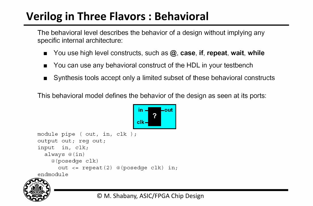
Verilog in Three Flavors : Behavioral
© M. Shabany, ASIC/FPGA Chip Design
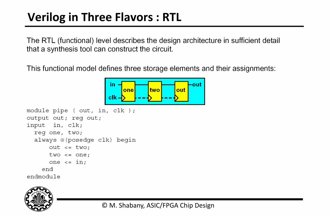
Verilog in Three Flavors : RTL
© M. Shabany, ASIC/FPGA Chip Design
Verilog in Three Flavors : Structural
© M. Shabany, ASIC/FPGA Chip Design
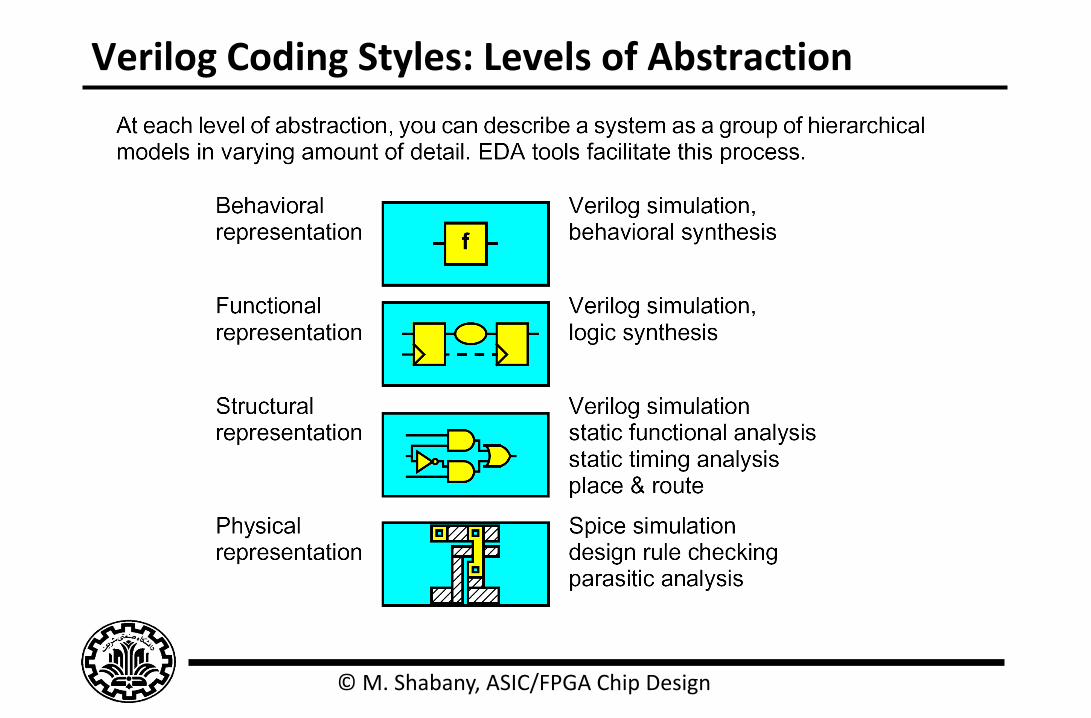
Verilog Coding Styles: Levels of Abstraction
© M. Shabany, ASIC/FPGA Chip Design
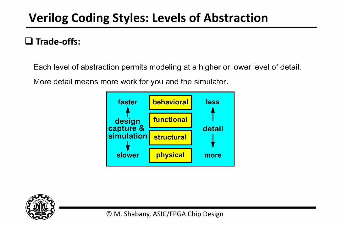
Verilog Coding Styles: Levels of Abstraction
Trade-offs:
© M. Shabany, ASIC/FPGA Chip Design
Verilog Coding Styles: Levels of Abstraction
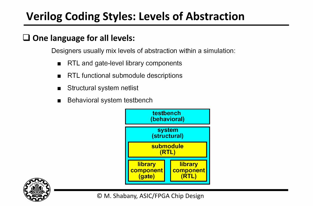
One language for all levels:
© M. Shabany, ASIC/FPGA Chip Design
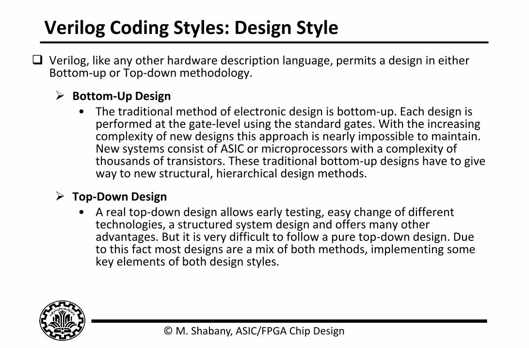
Verilog Coding Styles: Design Style
Verilog, like any other hardware description language, permits a design in either Bottom-up or Top-down methodology.
Bottom-Up Design • The traditional method of electronic design is bottom-up. Each design is
performed at the gate-level using the standard gates. With the increasing complexity of new designs this approach is nearly impossible to maintain. New systems consist of ASIC or microprocessors with a complexity of thousands of transistors. These traditional bottom-up designs have to give way to new structural, hierarchical design methods.
Top-Down Design • A real top-down design allows early testing, easy change of different
technologies, a structured system design and offers many other advantages. But it is very difficult to follow a pure top-down design. Due to this fact most designs are a mix of both methods, implementing some key elements of both design styles.
© M. Shabany, ASIC/FPGA Chip Design
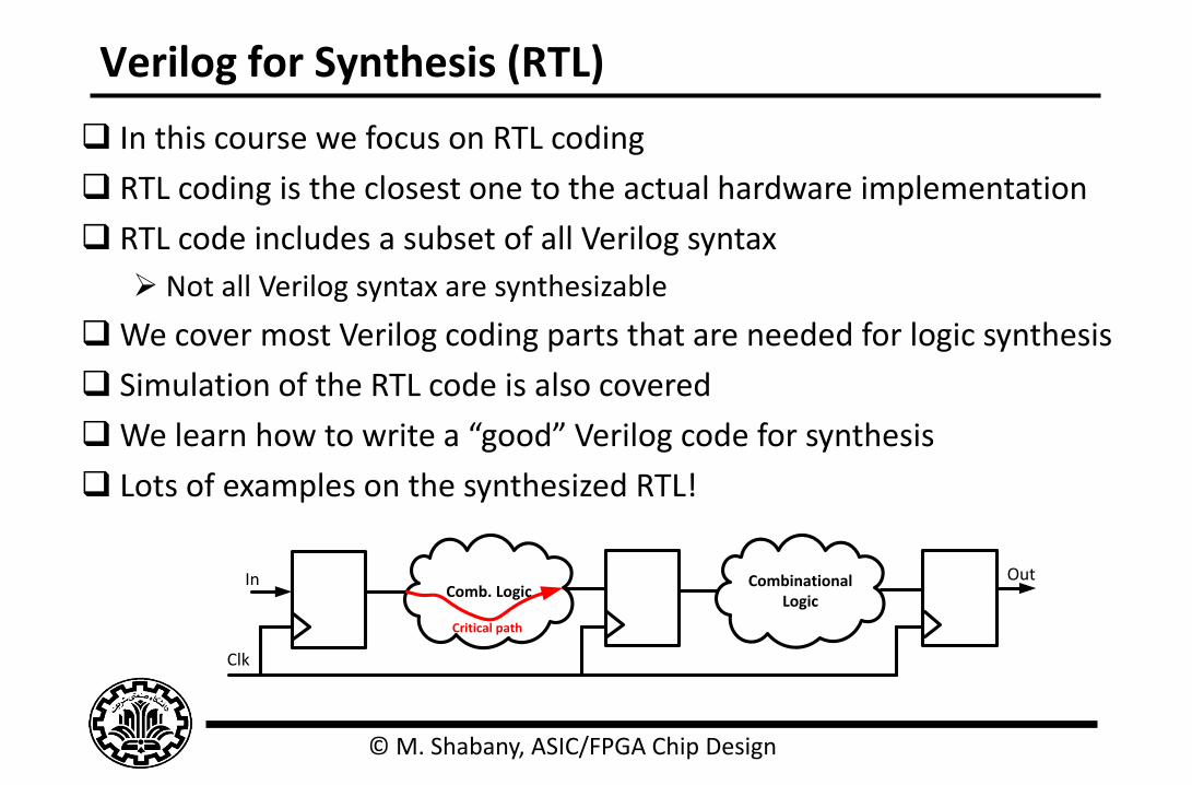
Verilog for Synthesis (RTL)
In this course we focus on RTL coding
RTL coding is the closest one to the actual hardware implementation
RTL code includes a subset of all Verilog syntax
Not all Verilog syntax are synthesizable
We cover most Verilog coding parts that are needed for logic synthesis
Simulation of the RTL code is also covered
We learn how to write a “good” Verilog code for synthesis
Lots of examples on the synthesized RTL!
Comb. LogicCombinational
Logic
Clk
In Out
Critical path
© M. Shabany, ASIC/FPGA Chip Design
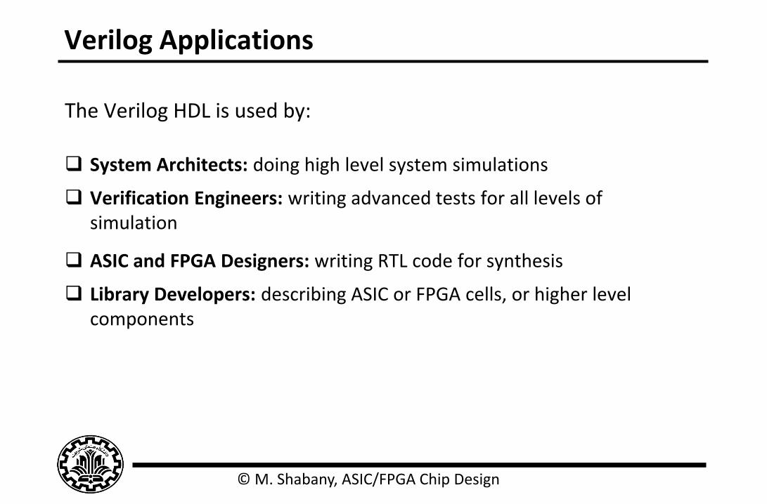
Verilog Applications
The Verilog HDL is used by:
System Architects: doing high level system simulations
Verification Engineers: writing advanced tests for all levels of simulation
ASIC and FPGA Designers: writing RTL code for synthesis
Library Developers: describing ASIC or FPGA cells, or higher level components
© M. Shabany, ASIC/FPGA Chip Design
Outline
ASIC/FPGA Design Flow
Hardware Description Language (HDL)
Verilog
o Introduction
o Language Fundamentals
o Modeling Combinational & Sequential Logic Circuits
o Modeling Finite State Machines
o Verilog Styles for Synthesis
o Testbench and Simulation
39
© M. Shabany, ASIC/FPGA Chip Design
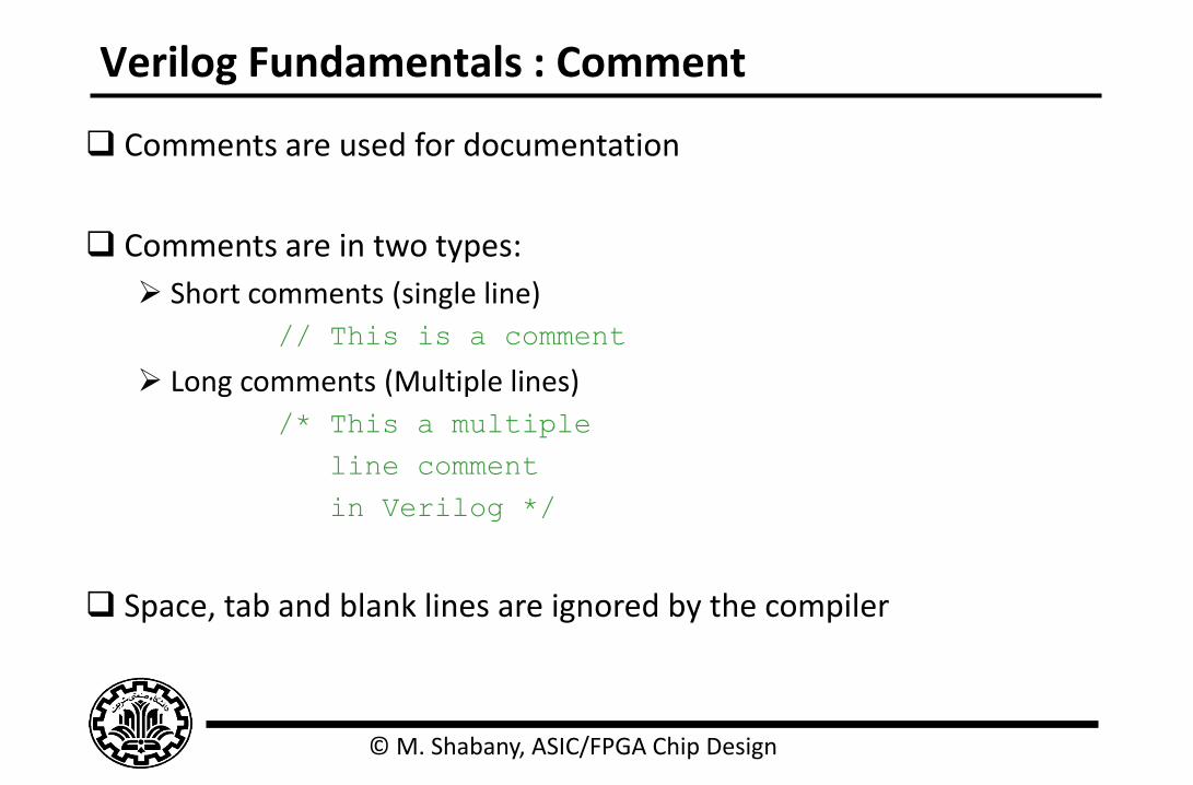
Verilog Fundamentals : Comment
Comments are used for documentation
Comments are in two types:
Short comments (single line)
// This is a comment
Long comments (Multiple lines)
/* This a multiple
line comment
in Verilog */
Space, tab and blank lines are ignored by the compiler
© M. Shabany, ASIC/FPGA Chip Design
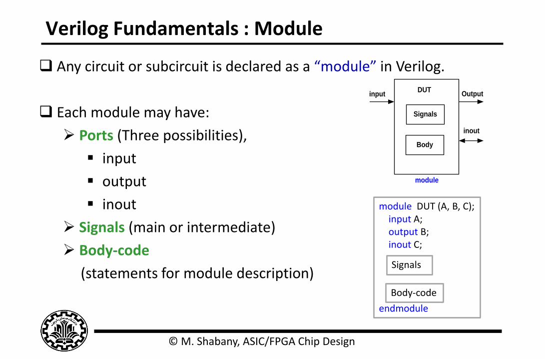
Verilog Fundamentals : Module
Any circuit or subcircuit is declared as a “module” in Verilog.
Each module may have:
Ports (Three possibilities),
input
output
inout
Signals (main or intermediate)
Body-code
(statements for module description)
module DUT (A, B, C); input A; output B; inout C; endmodule
Signals
Body-code
Signals
Body
DUTinput Output
inout
module

© M. Shabany, ASIC/FPGA Chip Design
Verilog Fundamentals : Signals
Signal
Type Range Name Value
Net Variable
wire tri reg integer
Scalar Vector
[3:0]
Example: wire [2:0] tmp ; tmp = 3’b001;
tmp[0]=1 tmp[1]=0 tmp[2]=0
Each element of a vector
can be accessed
© M. Shabany, ASIC/FPGA Chip Design
Verilog Fundamentals : Signal Type Net
wire: For interconnecting logic elements (LEs)
To connect an output of a logic element to the input of another LE
tri Circuit nodes that are connected in a tri-state fashion
Variable
reg (unsigned in general) Corresponds to a circuit node (not necessarily a register!)
Allow a circuit to be described in terms of its behavior
Retains its value until it is overwritten by a subsequent assignment
integer (signed in general) Used for loop counters
Signal
Type Range Name Value
© M. Shabany, ASIC/FPGA Chip Design
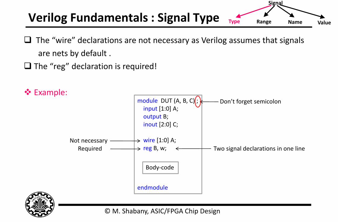
Verilog Fundamentals : Signal Type
The “wire” declarations are not necessary as Verilog assumes that signals
are nets by default .
The “reg” declaration is required!
Example: module DUT (A, B, C) ; input [1:0] A; output B; inout [2:0] C; wire [1:0] A; reg B, w; endmodule
Body-code
Not necessary Required Two signal declarations in one line
Signal
Type Range Name Value
Don’t forget semicolon
© M. Shabany, ASIC/FPGA Chip Design
Verilog Fundamentals : Signal Type
Example:
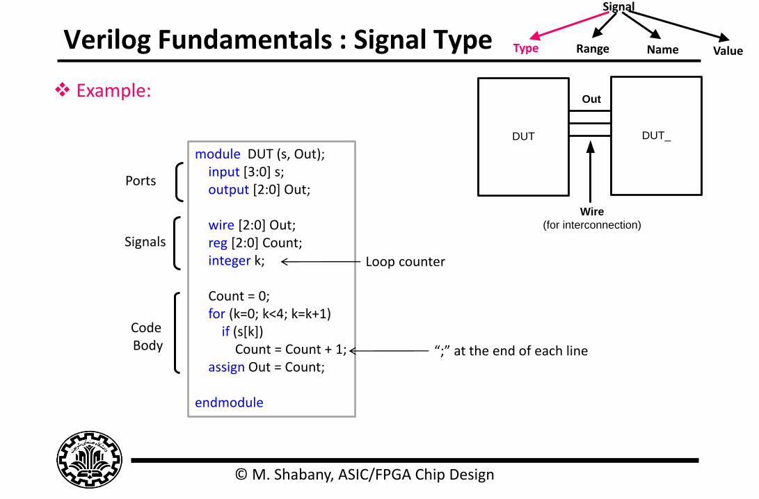
module DUT (s, Out); input [3:0] s; output [2:0] Out; wire [2:0] Out; reg [2:0] Count; integer k; Count = 0; for (k=0; k<4; k=k+1) if (s[k]) Count = Count + 1; assign Out = Count; endmodule
Loop counter
Ports
Signals
Code Body “;” at the end of each line
DUT
Out
DUT_
Wire
(for interconnection)
Signal
Type Range Name Value
© M. Shabany, ASIC/FPGA Chip Design
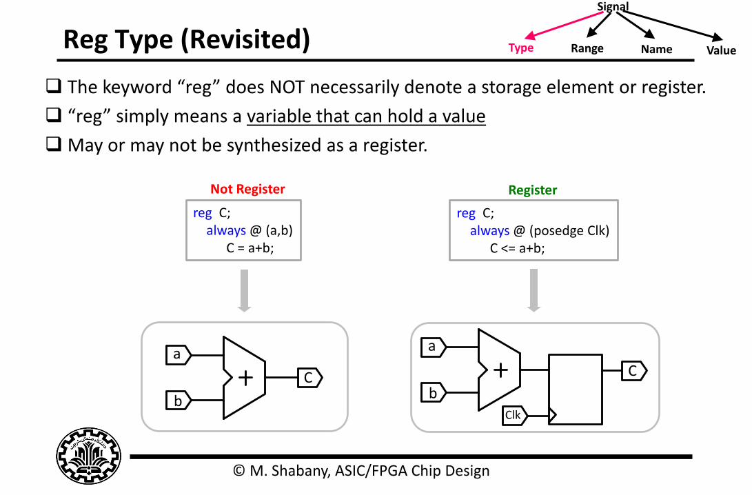
Reg Type
The keyword “reg” does NOT necessarily denote a storage element or register.
“reg” only models the behavior of a circuit.
May or may not be synthesized as a register.
reg C; always @ (a,b) C = a+b;
reg C; always @ (posedge Clk) C <= a+b;
a
b
C
Clk
a
b
C
Register Not Register
Signal
Type Range Name Value
© M. Shabany, ASIC/FPGA Chip Design
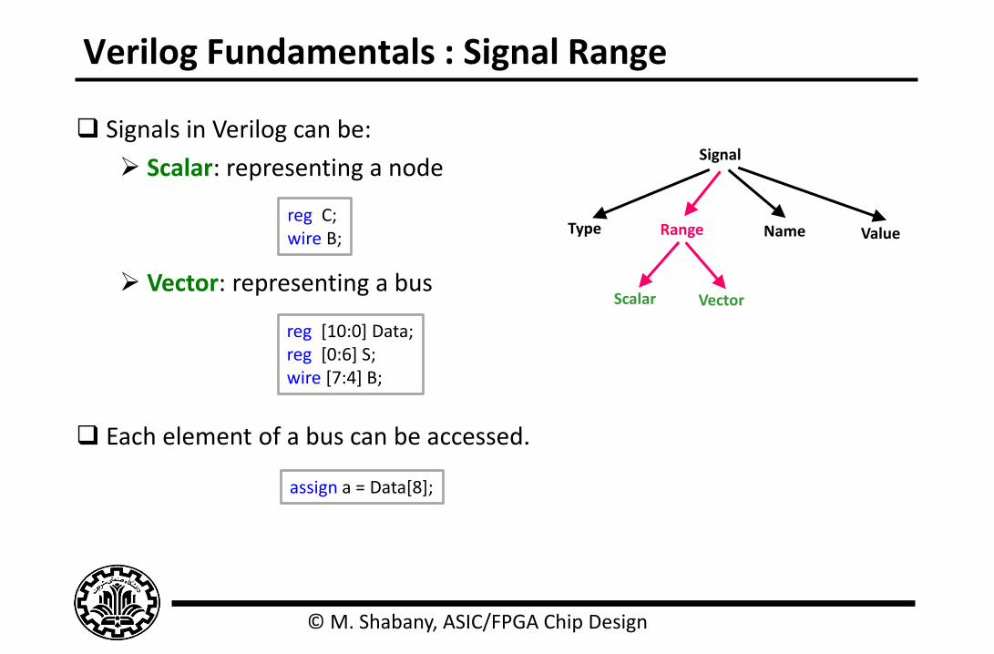
Verilog Fundamentals : Signal Range
Signals in Verilog can be:
Scalar: representing a node
Vector: representing a bus
Each element of a bus can be accessed.
reg C; wire B;
reg [10:0] Data; reg [0:6] S; wire [7:4] B;
assign a = Data[8];
Signal
Type Range Name Value
Scalar Vector
© M. Shabany, ASIC/FPGA Chip Design
Verilog Fundamentals : Signal Name
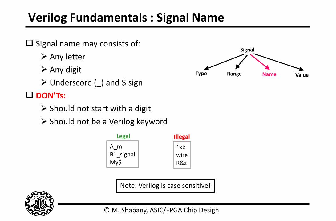
Signal name may consists of:
Any letter
Any digit
Underscore (_) and $ sign
DON’Ts:
Should not start with a digit
Should not be a Verilog keyword
A_m B1_signal My$
Signal
Type Range Name Value
1xb wire R&z
Illegal Legal
Note: Verilog is case sensitive!
© M. Shabany, ASIC/FPGA Chip Design
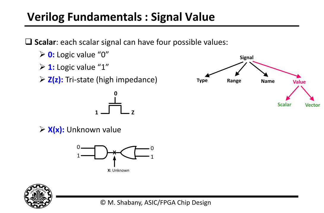
Verilog Fundamentals : Signal Value
Scalar: each scalar signal can have four possible values:
0: Logic value “0”
1: Logic value “1”
Z(z): Tri-state (high impedance)
X(x): Unknown value
Signal
Type Range Name Value
Scalar Vector
0
10
1
X: Unknown
X
0
1 Z
© M. Shabany, ASIC/FPGA Chip Design
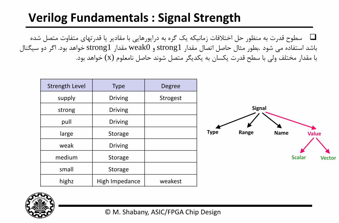
Verilog Fundamentals : Signal Strength
Signal
Type Range Name Value
Scalar Vector
Degree Type Strength Level
Strogest Driving supply
Driving strong
Driving pull
Storage large
Driving weak
Storage medium
Storage small
weakest High Impedance highz
شذه متصل قذرتهاي متفاوت يا مقادير با درايورهايي به گره يك زمانيكه فاتاختال حل منظور به قذرت سطوح
سيگنال دو اگر. خواهذ بود strong1مقذار weak0و strong1مقذار اتصال حاصل مثال بطور .شود مي استفاده باشذ
.خواهذ بود (x)نامعلوم حاصل شونذ متصل يكذيگر به يكسان سطح قذرت با ولي مختلف مقذار با
© M. Shabany, ASIC/FPGA Chip Design
Verilog Fundamentals : Signal Value
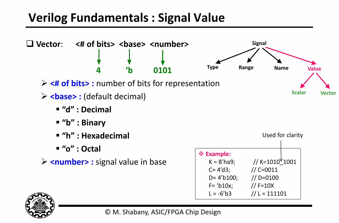
Vector: <# of bits> <base> <number>
4 ‘b 0101
<# of bits> : number of bits for representation
<base> : (default decimal)
“d” : Decimal
“b” : Binary
“h” : Hexadecimal
“o” : Octal
<number> : signal value in base
Signal
Type Range Name Value
Scalar Vector
Example: K = 8’ha9; // K=1010_1001 C= 4’d3; // C=0011 D= 4’b100; // D=0100 F= ‘b10x; // F=10X L = -6’b3 // L = 111101
Used for clarity
© M. Shabany, ASIC/FPGA Chip Design
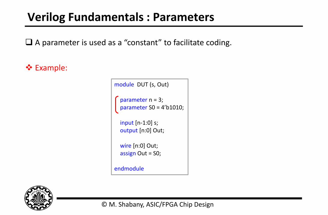
Verilog Fundamentals : Parameters
A parameter is used as a “constant” to facilitate coding.
Example:
module DUT (s, Out) parameter n = 3; parameter S0 = 4’b1010; input [n-1:0] s; output [n:0] Out; wire [n:0] Out; assign Out = S0; endmodule
© M. Shabany, ASIC/FPGA Chip Design
Verilog Fundamentals : Memories
Memory:
A two-dimensional array of bits
Declared in Verilog as a two-dimensional variable (reg)
Example: A 4-byte memory:
reg [7:0] R [3:0];
8-bit 4 rows (cell)
0 1 72 3 4 5 6
R[0]
R[1]
R[2]
R[3]
R[2][5](indexing method) A three-dimensional array may also be declared.
Example:
If an 8-bit A is declared then the legal assignment is:
reg [7:0] M [3:0][1:0];
reg [7:0] A; A = M[3][0];
© M. Shabany, ASIC/FPGA Chip Design
Verilog Fundamentals : Operators
Example:
Bitwise:
Logical:
Operation Result
1010 & 1100 1000
1010 | 1100 1110
~1010 0101
1101 Λ 0100 1001
Operation Result
1010 && 1100 1
2’b11 || 2’b00 1
!0010 0
2’b1X && 2’b11 X
Non-zero operand=logical “1”
Any operand X/Z, result is X
X || 1 = 1 X && 0 = 0
1 0 1 0
1 1 0 0
1 0 0 0
&

© M. Shabany, ASIC/FPGA Chip Design
Verilog Fundamentals : Operators
Example:
Reduction:
Relational:
Operation Result
& 1100 0
& 111 1
Λ 0100 1
Operation Result
B=(A == 2’b10) B=1
B=(A == 2’b11) B=0
B=(A === 2’b1x) B=0
B=(A <= 2’b11) B=1
=== Used with x and z
A=2’b10
== Used only with 0 and 1

© M. Shabany, ASIC/FPGA Chip Design
Verilog Fundamentals : Operators
Example:
Logical Shift:
Concatenation:
Operation Result
C = A >> 1 C = 000110
D = A << 2 D = 110000
F = A >> 3 F = 000001
Operation Result
{A, B} 5’b11010
{3{A}} 6’b111111
{B, B} 6’b010010
{{3{A}}, {2{B}}} 12’b111111010010
A=2’b11 B=3’b010
A=6’b001100
Be generous in {}
© M. Shabany, ASIC/FPGA Chip Design
Verilog Fundamentals : Operators
Conditional: (? , : )
D = S ? B:C;
D = ({S1,S2}==2’b00)? F:
({S1,S2}==2’b01)? E:
({S1,S2}==2’b10)? C:B;
C
D
B
S
0
1B if S=1; C if S=0;
D =
CD
B
S1
00
11
01
10
E
F
S2
4-input Multiplexer
(MUX) D = ({S1,S2}==2’b00)? F:
({S1,S2}==2’b01)? E:
({S1,S2}==2’b10)? C:
({S1,S2}==2’b11)? B:B;
Default
© M. Shabany, ASIC/FPGA Chip Design
Verilog Fundamentals : Operators (All in One)
© M. Shabany, ASIC/FPGA Chip Design
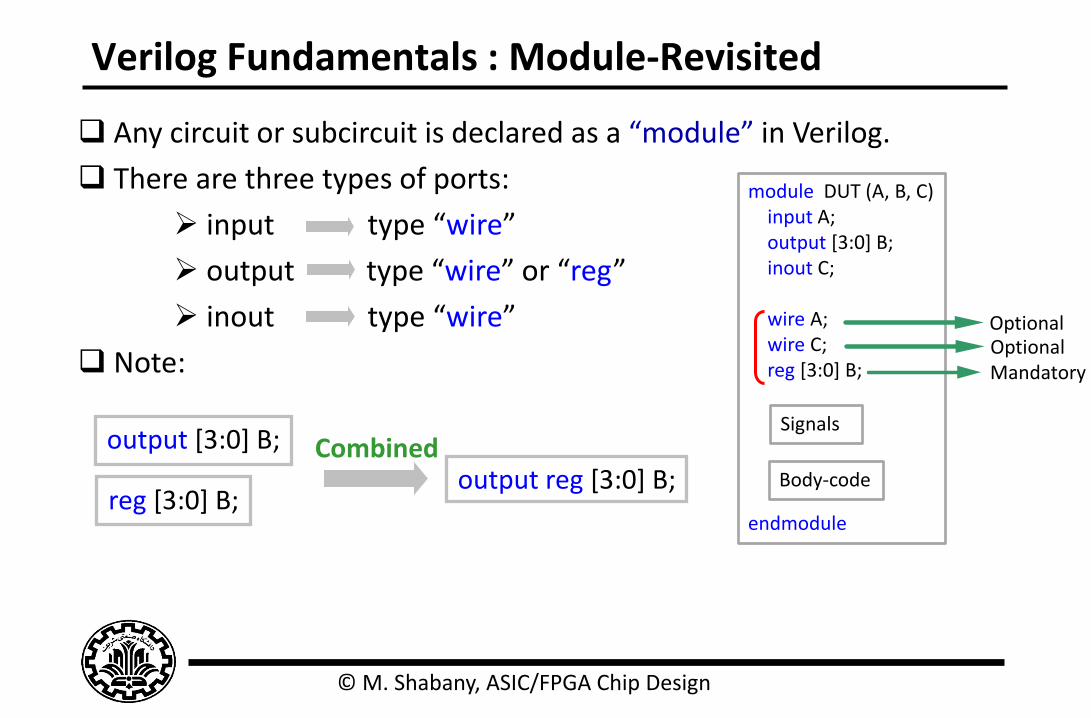
Verilog Fundamentals : Module-Revisited
Any circuit or subcircuit is declared as a “module” in Verilog.
There are three types of ports:
input type “wire”
output type “wire” or “reg”
inout type “wire”
Note:
module DUT (A, B, C) input A; output [3:0] B; inout C; wire A; wire C; reg [3:0] B; endmodule
Signals
Body-code
Optional Optional Mandatory
output [3:0] B;
reg [3:0] B; output reg [3:0] B;
Combined
© M. Shabany, ASIC/FPGA Chip Design
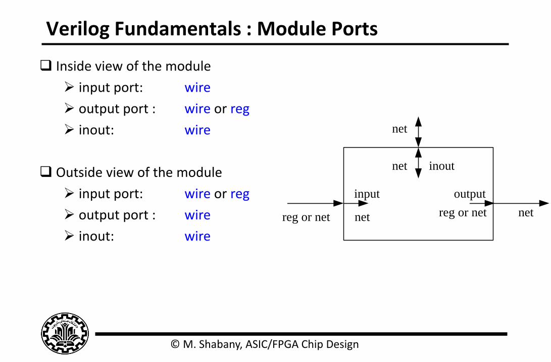
Verilog Fundamentals : Module Ports
net
net inout
net netreg or net reg or net
input output
Inside view of the module
input port: wire
output port : wire or reg
inout: wire
Outside view of the module
input port: wire or reg
output port : wire
inout: wire
© M. Shabany, ASIC/FPGA Chip Design
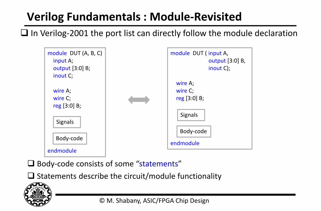
Verilog Fundamentals : Module-Revisited In Verilog-2001 the port list can directly follow the module declaration
module DUT (A, B, C) input A; output [3:0] B; inout C; wire A; wire C; reg [3:0] B; endmodule
Signals
Body-code
module DUT ( input A, output [3:0] B, inout C); wire A; wire C; reg [3:0] B; endmodule
Signals
Body-code
Body-code consists of some “statements”
Statements describe the circuit/module functionality
© M. Shabany, ASIC/FPGA Chip Design
Verilog Fundamentals : Statements
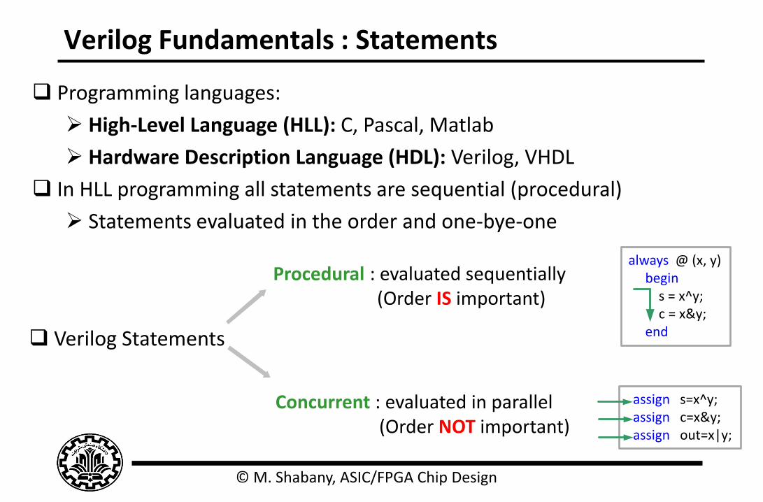
Programming languages:
High-Level Language (HLL): C, Pascal, Matlab
Hardware Description Language (HDL): Verilog, VHDL
In HLL programming all statements are sequential (procedural)
Statements evaluated in the order and one-bye-one
Procedural : evaluated sequentially (Order IS important)
Concurrent : evaluated in parallel (Order NOT important)
always @ (x, y) begin s = x^y; c = x&y; end
assign s=x^y; assign c=x&y; assign out=x|y;
Verilog Statements
© M. Shabany, ASIC/FPGA Chip Design
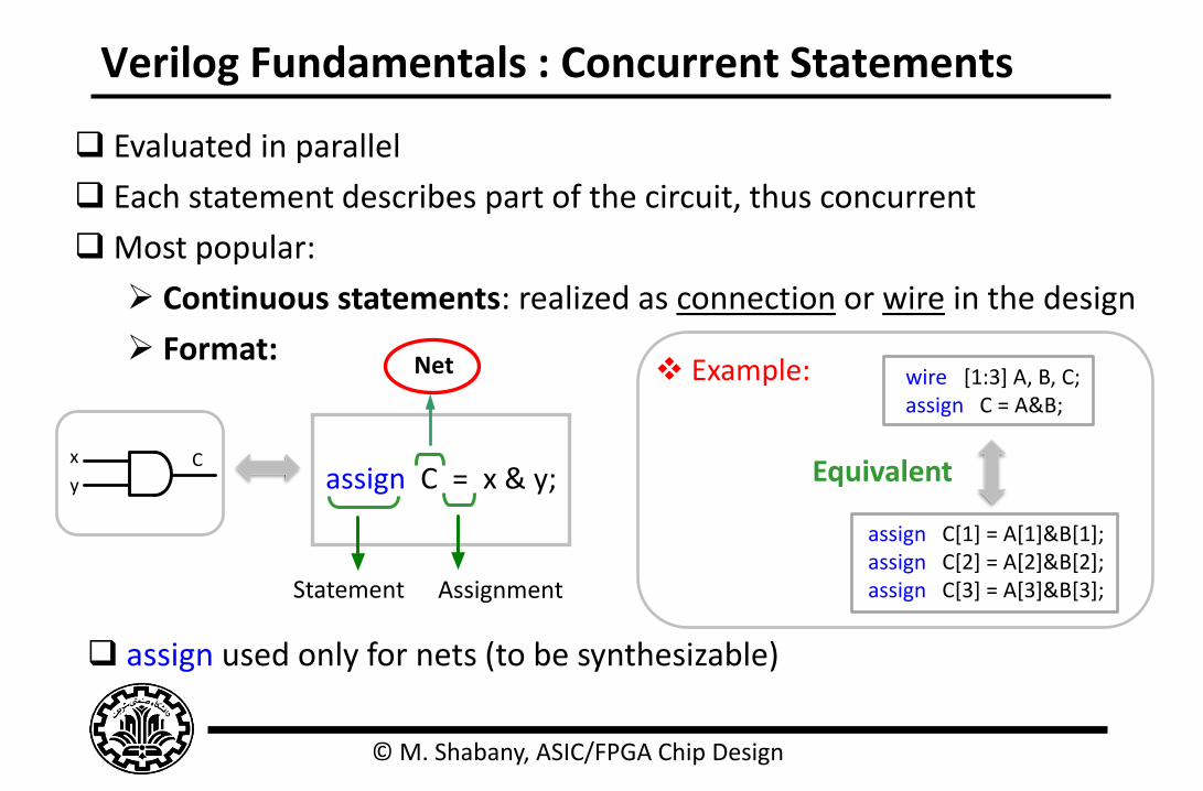
Verilog Fundamentals : Concurrent Statements
Evaluated in parallel
Each statement describes part of the circuit, thus concurrent
Most popular:
Continuous statements: realized as connection or wire in the design
Format: Example: wire [1:3] A, B, C;
assign C = A&B;
assign C = x & y;
Statement Assignment
Net
assign used only for nets (to be synthesizable)
assign C[1] = A[1]&B[1]; assign C[2] = A[2]&B[2]; assign C[3] = A[3]&B[3];
Equivalent x
y
C
© M. Shabany, ASIC/FPGA Chip Design
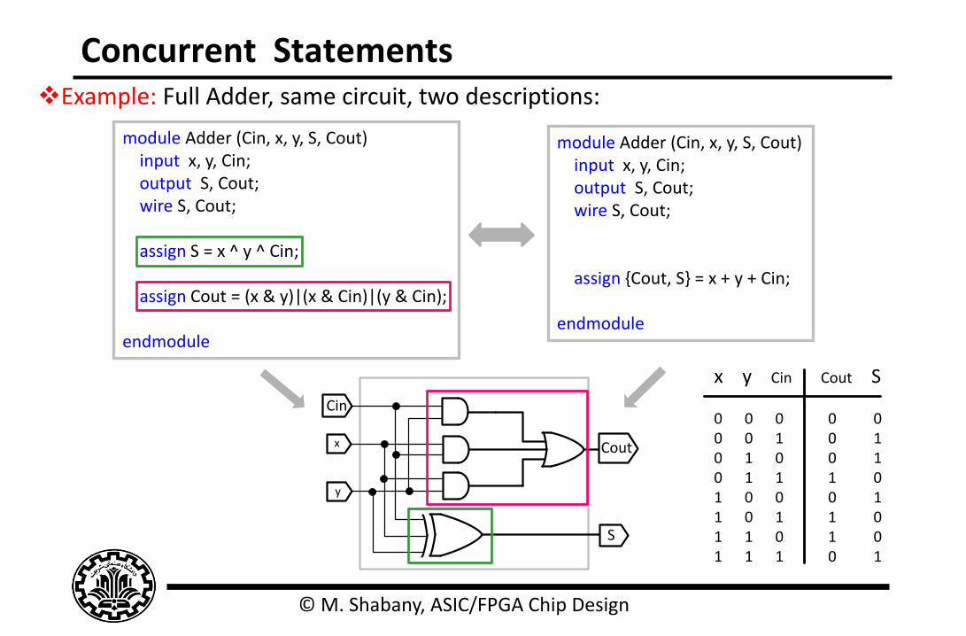
Concurrent Statements Example: Full Adder, same circuit, two descriptions:
module Adder (Cin, x, y, S, Cout) input x, y, Cin; output S, Cout; wire S, Cout; assign S = x ^ y ^ Cin; assign Cout = (x & y)|(x & Cin)|(y & Cin); endmodule
module Adder (Cin, x, y, S, Cout) input x, y, Cin; output S, Cout; wire S, Cout; assign {Cout, S} = x + y + Cin; endmodule
x
Cin
S
Cout
y
x y Cin Cout S
0 0 0 0 0 0 0 1 0 1 0 1 0 0 1 0 1 1 1 0 1 0 0 0 1 1 0 1 1 01 1 0 1 0 1 1 1 0 1
© M. Shabany, ASIC/FPGA Chip Design
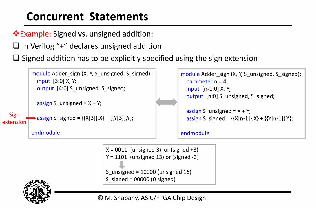
Concurrent Statements
Example: Signed vs. unsigned addition:
In Verilog “+” declares unsigned addition
Signed addition has to be explicitly specified using the sign extension
module Adder_sign (X, Y, S_unsigned, S_signed); input [3:0] X, Y; output [4:0] S_unsigned, S_signed; assign S_unsigned = X + Y; assign S_signed = {{X[3]},X} + {{Y[3]},Y}; endmodule
module Adder_sign (X, Y, S_unsigned, S_signed); parameter n = 4; input [n-1:0] X, Y; output [n:0] S_unsigned, S_signed; assign S_unsigned = X + Y; assign S_signed = {{X[n-1]},X} + {{Y[n-1]},Y}; endmodule
Sign extension
X = 0011 (unsigned 3) or (signed +3) Y = 1101 (unsigned 13) or (signed -3) S_unsigned = 10000 (unsigned 16) S_signed = 00000 (0 signed)
© M. Shabany, ASIC/FPGA Chip Design
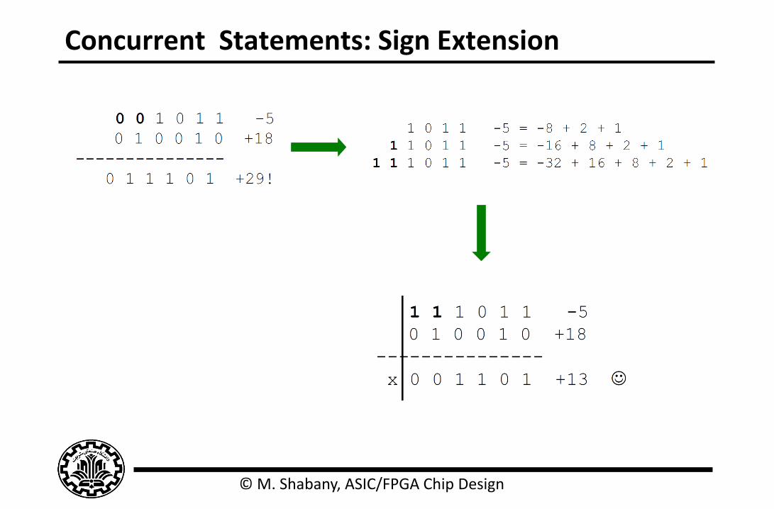
Concurrent Statements: Sign Extension
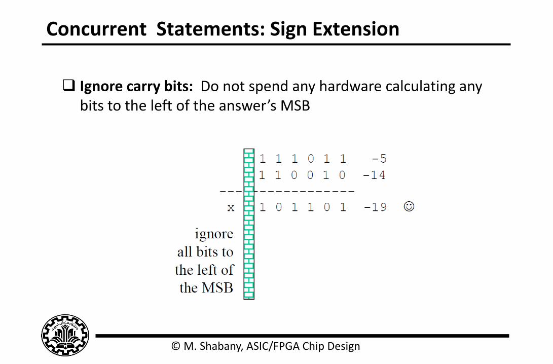
© M. Shabany, ASIC/FPGA Chip Design
Concurrent Statements: Sign Extension
Ignore carry bits: Do not spend any hardware calculating any bits to the left of the answer’s MSB

© M. Shabany, ASIC/FPGA Chip Design
Verilog Fundamentals : Delay
Delay can be used with continuous assignments by using the “#” sign
2 time unit of delay on wire S
5 time units of delay for AND gate
Any change in x or y reflects on S after 7 time unit delay
Used only for simulation purposes No meaning for synthesis Not synthesizable
wire #2 S; assign #5 S = x&y;
© M. Shabany, ASIC/FPGA Chip Design
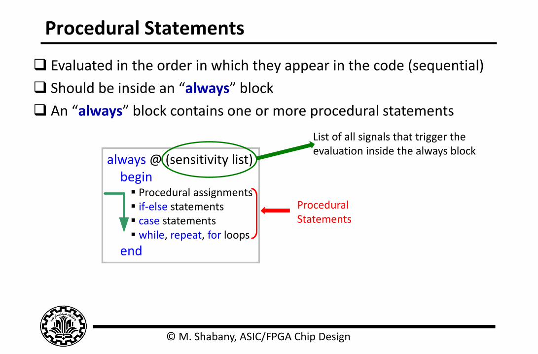
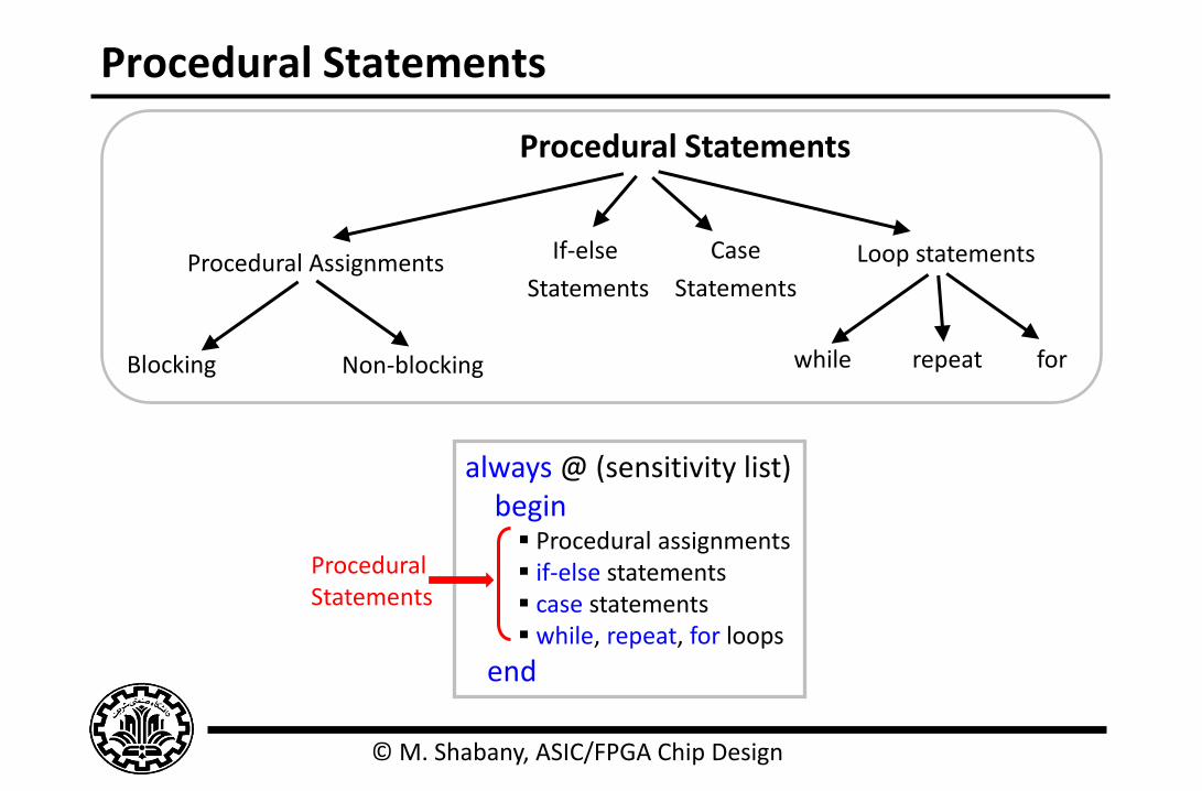
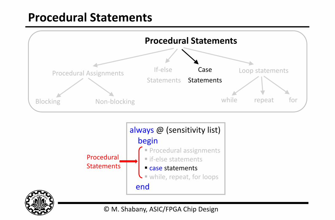
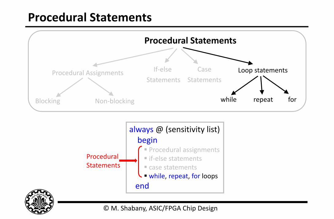
Procedural Statements
Evaluated in the order in which they appear in the code (sequential)
Should be inside an “always” block
An “always” block contains one or more procedural statements
always @ (sensitivity list) begin
Procedural assignments if-else statements case statements while, repeat, for loops
end
List of all signals that trigger the evaluation inside the always block
Procedural Statements
© M. Shabany, ASIC/FPGA Chip Design
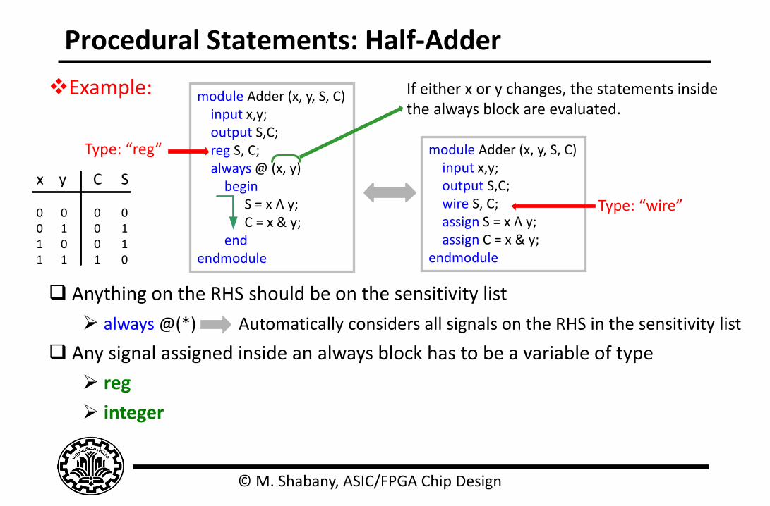
Procedural Statements: Half-Adder
Example:
Anything on the RHS should be on the sensitivity list
always @(*) Automatically considers all signals on the RHS in the sensitivity list
Any signal assigned inside an always block has to be a variable of type
reg
integer
module Adder (x, y, S, C) input x,y; output S,C; reg S, C; always @ (x, y) begin
S = x Λ y; C = x & y;
end endmodule
module Adder (x, y, S, C) input x,y; output S,C; wire S, C; assign S = x Λ y; assign C = x & y; endmodule
If either x or y changes, the statements inside the always block are evaluated.
Type: “reg”
Type: “wire”
x y C S
0 0 0 0 0 1 0 1 1 0 0 1 1 1 1 0
© M. Shabany, ASIC/FPGA Chip Design
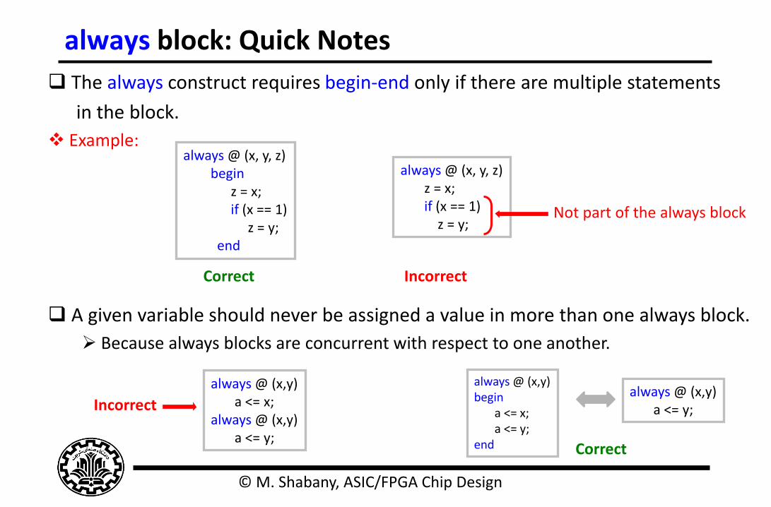
always block: Quick Notes
The always construct requires begin-end only if there are multiple statements
in the block.
Example:
A given variable should never be assigned a value in more than one always block.
Because always blocks are concurrent with respect to one another.
always @ (x, y, z) begin
z = x; if (x == 1) z = y; end
Not part of the always block
Incorrect
always @ (x, y, z) z = x; if (x == 1)
z = y;
Correct
always @ (x,y) a <= x; always @ (x,y) a <= y;
Incorrect always @ (x,y) a <= y;
Correct
always @ (x,y) begin a <= x; a <= y; end
© M. Shabany, ASIC/FPGA Chip Design
Procedural Statements
always @ (sensitivity list) begin
Procedural assignments if-else statements case statements while, repeat, for loops
end
Procedural Statements
Procedural Statements
Procedural Assignments If-else
Statements
Case
Statements
while repeat for
Loop statements
Blocking Non-blocking
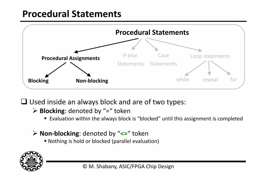
© M. Shabany, ASIC/FPGA Chip Design
Procedural Statements
Procedural Statements
Procedural Assignments If-else
Statements
Case
Statements
while repeat for
Loop statements
Blocking Non-blocking
Used inside an always block and are of two types: Blocking: denoted by “=“ token
Evaluation within the always block is “blocked” until this assignment is completed
Non-blocking: denoted by “<=“ token Nothing is hold or blocked (parallel evaluation)
© M. Shabany, ASIC/FPGA Chip Design
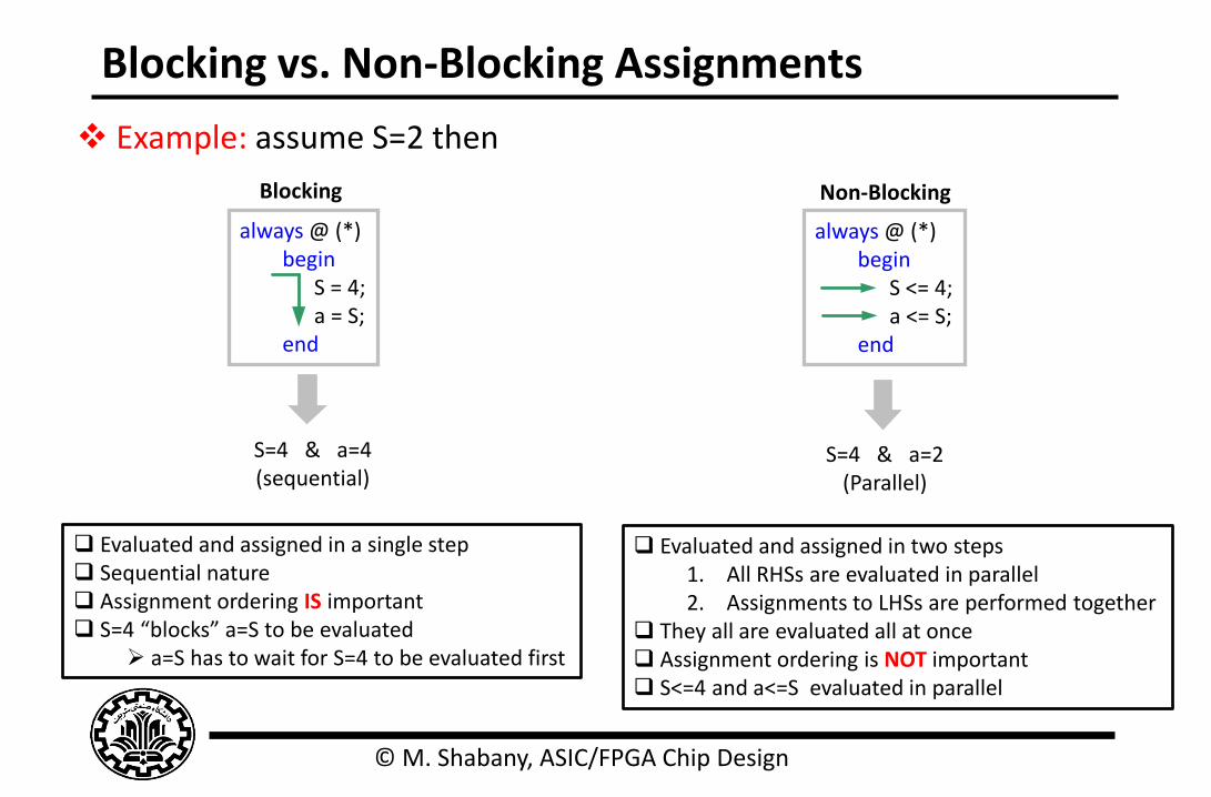
Blocking vs. Non-Blocking Assignments
Example: assume S=2 then
always @ (*) begin
S = 4; a = S;
end
always @ (*) begin
S <= 4; a <= S;
end
S=4 & a=4 (sequential)
S=4 & a=2 (Parallel)
Blocking Non-Blocking
Evaluated and assigned in a single step Sequential nature Assignment ordering IS important S=4 “blocks” a=S to be evaluated
a=S has to wait for S=4 to be evaluated first
Evaluated and assigned in two steps 1. All RHSs are evaluated in parallel 2. Assignments to LHSs are performed together
They all are evaluated all at once Assignment ordering is NOT important S<=4 and a<=S evaluated in parallel
© M. Shabany, ASIC/FPGA Chip Design
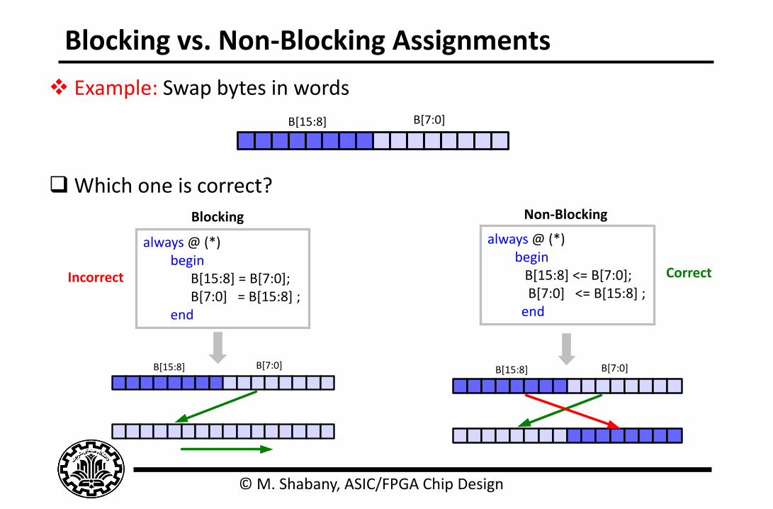
Blocking vs. Non-Blocking Assignments
Example: Swap bytes in words
Which one is correct?
always @ (*) begin
B[15:8] = B[7:0]; B[7:0] = B[15:8] ;
end
always @ (*) begin
B[15:8] <= B[7:0]; B[7:0] <= B[15:8] ; end
Blocking Non-Blocking
B[15:8] B[7:0]
Incorrect Correct
B[15:8] B[7:0]
B[15:8] B[7:0]
© M. Shabany, ASIC/FPGA Chip Design
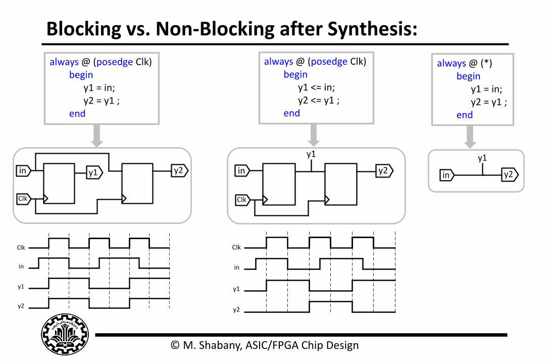
Blocking vs. Non-Blocking after Synthesis:
always @ (posedge Clk) begin
y1 = in; y2 = y1 ;
end
always @ (posedge Clk) begin
y1 <= in; y2 <= y1 ;
end
Clk
in y2y1
Clk
in y2
y1
Clk
in
y1
y2
Clk
in
y1
y2
always @ (*) begin
y1 = in; y2 = y1 ;
end
in y2
y1
© M. Shabany, ASIC/FPGA Chip Design
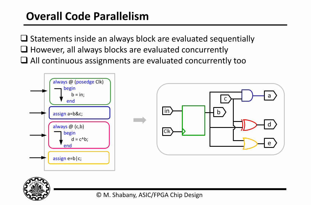
Overall Code Parallelism
always @ (posedge Clk) begin
b = in; end
assign a=b&c; always @ (c,b) begin
d = c^b; end assign e=b|c;
Statements inside an always block are evaluated sequentially However, all always blocks are evaluated concurrently All continuous assignments are evaluated concurrently too
C
Clk
in b
a
d
e
© M. Shabany, ASIC/FPGA Chip Design
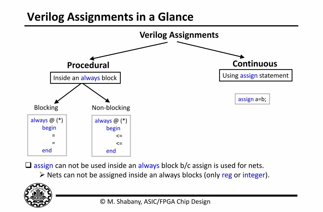
Verilog Assignments in a Glance
Verilog Assignments
Continuous Procedural
Blocking Non-blocking
Using assign statement Inside an always block
always @ (*) begin
<= <=
end
always @ (*) begin
= =
end
assign a=b;
assign can not be used inside an always block b/c assign is used for nets. Nets can not be assigned inside an always blocks (only reg or integer).
© M. Shabany, ASIC/FPGA Chip Design
Outline
ASIC/FPGA Design Flow
Hardware Description Language (HDL)
Verilog
o Introduction
o Language Fundamentals
o Modeling Combinational & Sequential Logic Circuits
o Modeling Finite State Machines
o Verilog Operations
79
© M. Shabany, ASIC/FPGA Chip Design
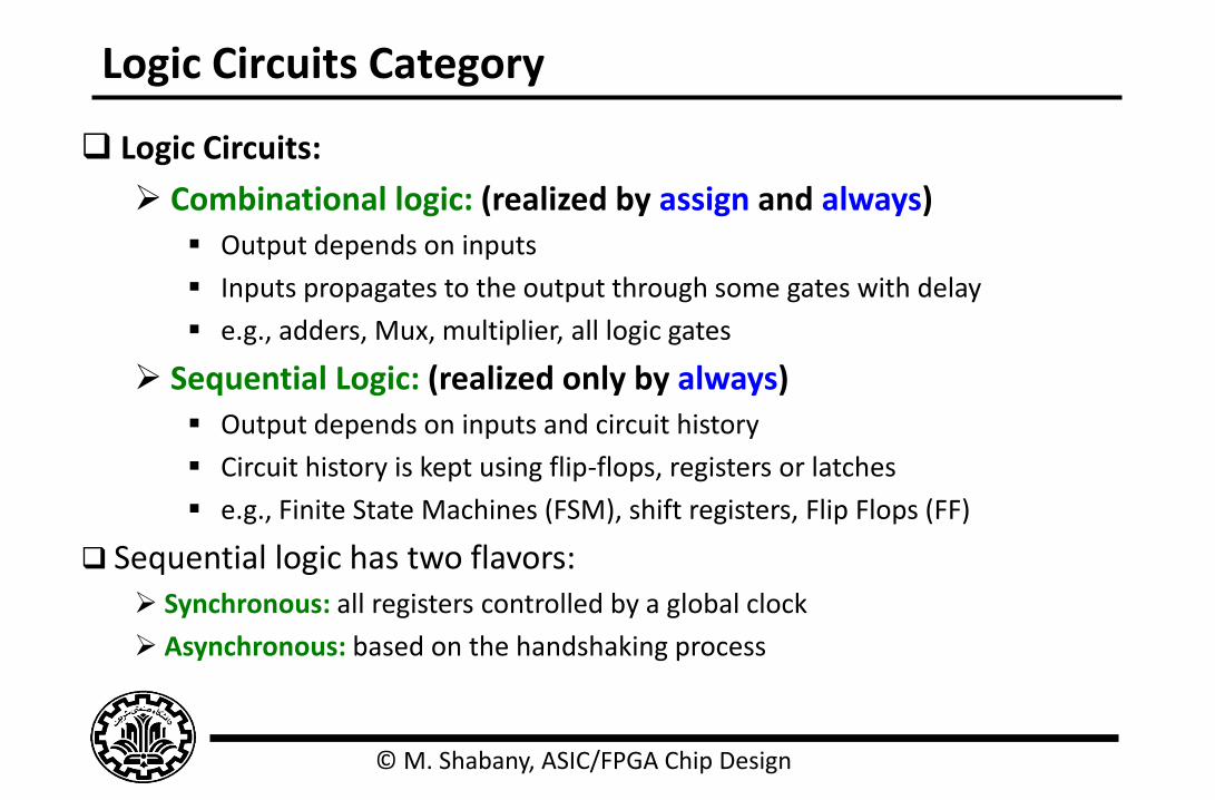
Logic Circuits Category
Logic Circuits:
Combinational logic: (realized by assign and always) Output depends on inputs
Inputs propagates to the output through some gates with delay
e.g., adders, Mux, multiplier, all logic gates
Sequential Logic: (realized only by always) Output depends on inputs and circuit history
Circuit history is kept using flip-flops, registers or latches
e.g., Finite State Machines (FSM), shift registers, Flip Flops (FF)
Sequential logic has two flavors: Synchronous: all registers controlled by a global clock
Asynchronous: based on the handshaking process
© M. Shabany, ASIC/FPGA Chip Design
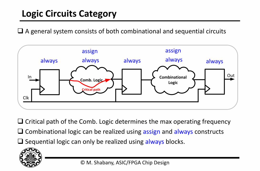
Logic Circuits Category
A general system consists of both combinational and sequential circuits
Critical path of the Comb. Logic determines the max operating frequency
Combinational logic can be realized using assign and always constructs
Sequential logic can only be realized using always blocks.
Comb. LogicCombinational
Logic
Clk
In Out
Critical path
always
assign
always
assign
always always always
© M. Shabany, ASIC/FPGA Chip Design
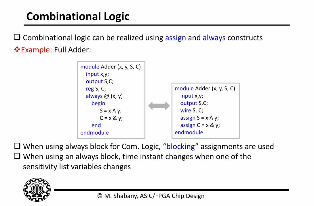
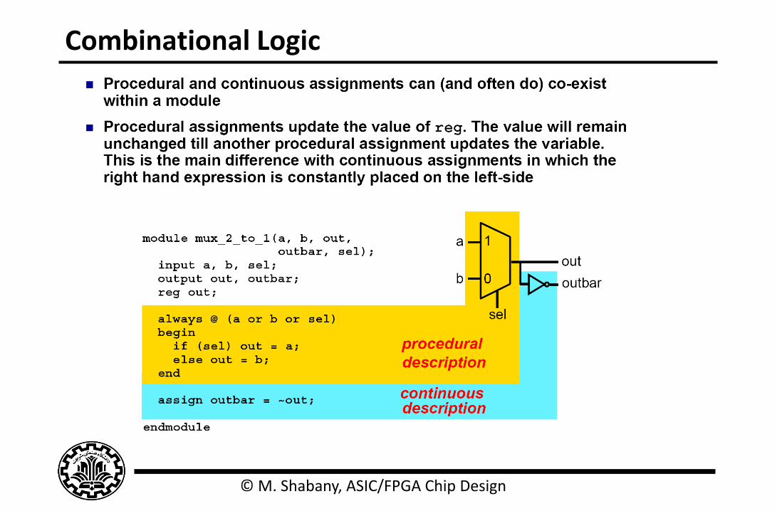
Combinational Logic
Combinational logic can be realized using assign and always constructs
Example: Full Adder:
When using always block for Com. Logic, “blocking” assignments are used When using an always block, time instant changes when one of the sensitivity list variables changes
module Adder (x, y, S, C) input x,y; output S,C; reg S, C; always @ (x, y) begin
S = x Λ y; C = x & y;
end endmodule
module Adder (x, y, S, C) input x,y; output S,C; wire S, C; assign S = x Λ y; assign C = x & y; endmodule
© M. Shabany, ASIC/FPGA Chip Design
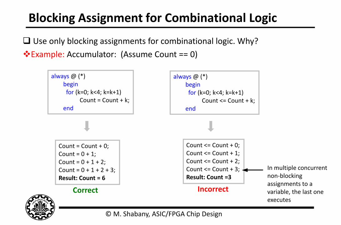
Blocking Assignment for Combinational Logic
Use only blocking assignments for combinational logic. Why?
Example: Accumulator: (Assume Count == 0)
always @ (*) begin
for (k=0; k<4; k=k+1) Count = Count + k;
end
always @ (*) begin
for (k=0; k<4; k=k+1) Count <= Count + k;
end
Count = Count + 0; Count = 0 + 1; Count = 0 + 1 + 2; Count = 0 + 1 + 2 + 3; Result: Count = 6
Count <= Count + 0; Count <= Count + 1; Count <= Count + 2; Count <= Count + 3; Result: Count =3
Incorrect Correct
In multiple concurrent non-blocking assignments to a variable, the last one executes
© M. Shabany, ASIC/FPGA Chip Design
Combinational Logic
© M. Shabany, ASIC/FPGA Chip Design
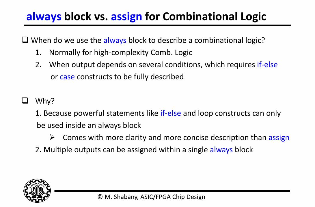
always block vs. assign for Combinational Logic
When do we use the always block to describe a combinational logic?
1. Normally for high-complexity Comb. Logic
2. When output depends on several conditions, which requires if-else
or case constructs to be fully described
Why?
1. Because powerful statements like if-else and loop constructs can only
be used inside an always block
Comes with more clarity and more concise description than assign
2. Multiple outputs can be assigned within a single always block
© M. Shabany, ASIC/FPGA Chip Design
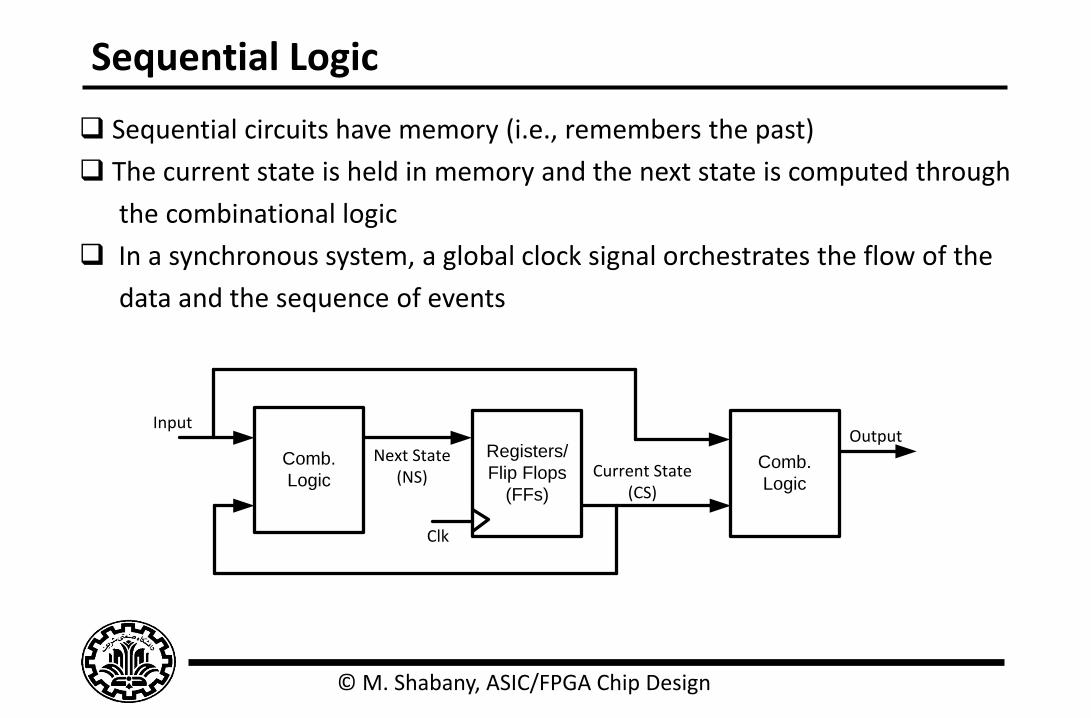
Sequential Logic
Sequential circuits have memory (i.e., remembers the past)
The current state is held in memory and the next state is computed through
the combinational logic
In a synchronous system, a global clock signal orchestrates the flow of the
data and the sequence of events
Comb.
Logic
Registers/
Flip Flops
(FFs)
Comb.
Logic
Input
Next State(NS) Current State
(CS)
Output
Clk
© M. Shabany, ASIC/FPGA Chip Design
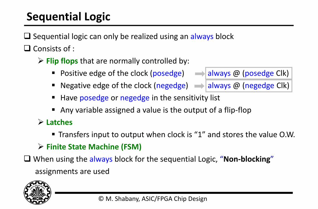
Sequential Logic
Sequential logic can only be realized using an always block
Consists of :
Flip flops that are normally controlled by:
Positive edge of the clock (posedge) always @ (posedge Clk)
Negative edge of the clock (negedge) always @ (negedge Clk)
Have posedge or negedge in the sensitivity list
Any variable assigned a value is the output of a flip-flop
Latches
Transfers input to output when clock is “1” and stores the value O.W.
Finite State Machine (FSM)
When using the always block for the sequential Logic, “Non-blocking”
assignments are used
© M. Shabany, ASIC/FPGA Chip Design
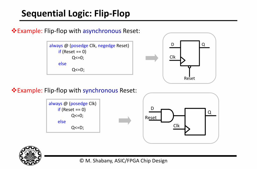
Sequential Logic: Flip-Flop
Example: Flip-flop with asynchronous Reset:
Example: Flip-flop with synchronous Reset:
always @ (posedge Clk, negedge Reset) if (Reset == 0) Q<=0; else Q<=D;
always @ (posedge Clk) if (Reset == 0) Q<=0; else Q<=D;
Clk
D Q
Reset
Clk
QD
Reset
© M. Shabany, ASIC/FPGA Chip Design
Sequential Logic: Flip-Flop
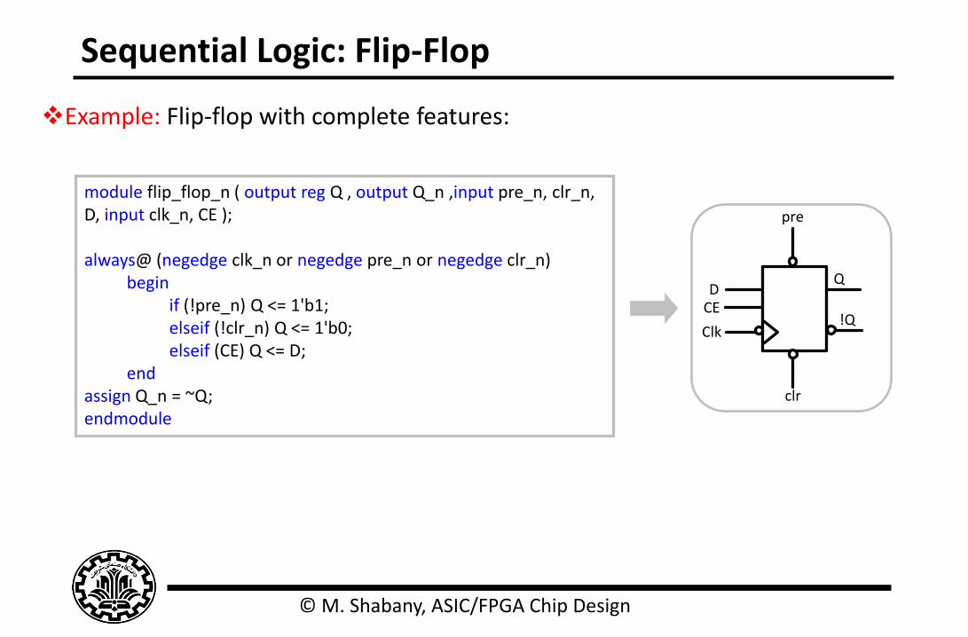
Example: Flip-flop with complete features:
module flip_flop_n ( output reg Q , output Q_n ,input pre_n, clr_n, D, input clk_n, CE ); always@ (negedge clk_n or negedge pre_n or negedge clr_n)
begin if (!pre_n) Q <= 1'b1; elseif (!clr_n) Q <= 1'b0; elseif (CE) Q <= D;
end assign Q_n = ~Q; endmodule
Clk
DQ
clr
CE
pre
!Q
© M. Shabany, ASIC/FPGA Chip Design
Sequential Logic: Flip-Flop
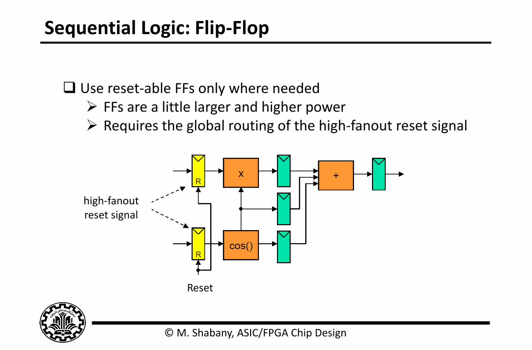
Use reset-able FFs only where needed FFs are a little larger and higher power Requires the global routing of the high-fanout reset signal
high-fanout reset signal
Reset
© M. Shabany, ASIC/FPGA Chip Design
Sequential Logic
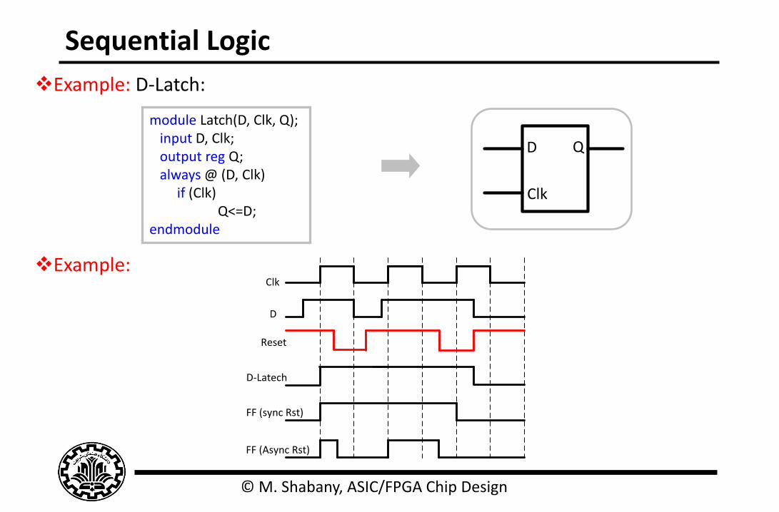
Example: D-Latch:
Example:
module Latch(D, Clk, Q); input D, Clk; output reg Q; always @ (D, Clk) if (Clk) Q<=D; endmodule
Q
Clk
D
Clk
D
D-Latech
FF (sync Rst)
FF (Async Rst)
Reset
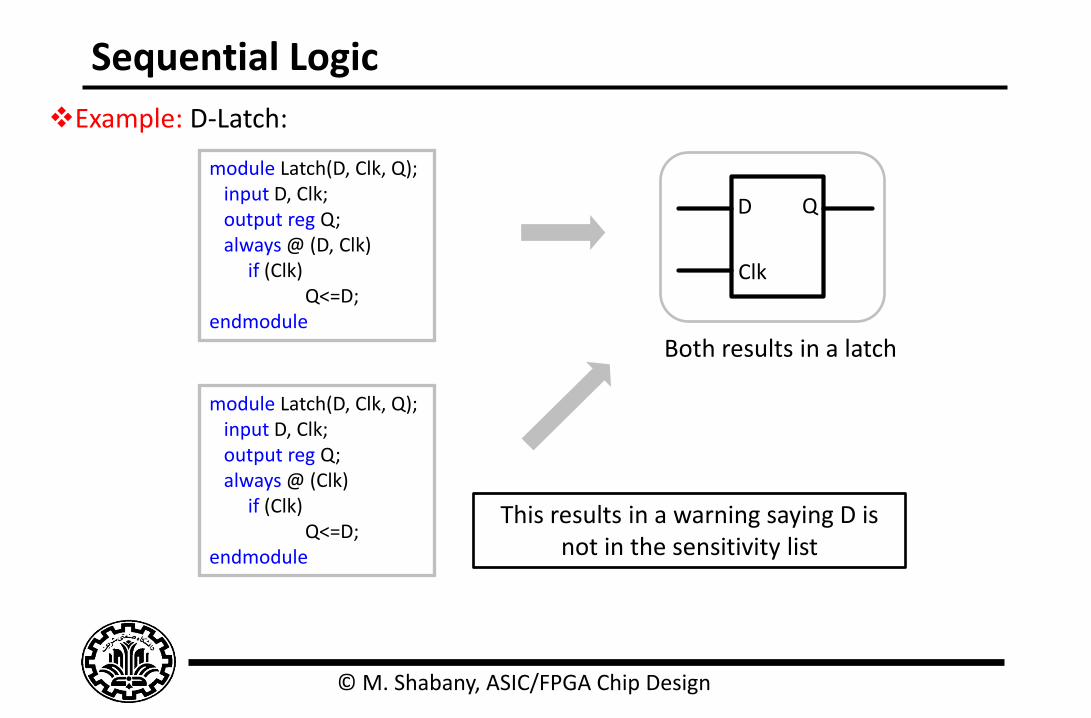
© M. Shabany, ASIC/FPGA Chip Design
Sequential Logic
Example: D-Latch:
module Latch(D, Clk, Q); input D, Clk; output reg Q; always @ (D, Clk) if (Clk) Q<=D; endmodule
Q
Clk
D
module Latch(D, Clk, Q); input D, Clk; output reg Q; always @ (Clk) if (Clk) Q<=D; endmodule
Both results in a latch
This results in a warning saying D is not in the sensitivity list
© M. Shabany, ASIC/FPGA Chip Design
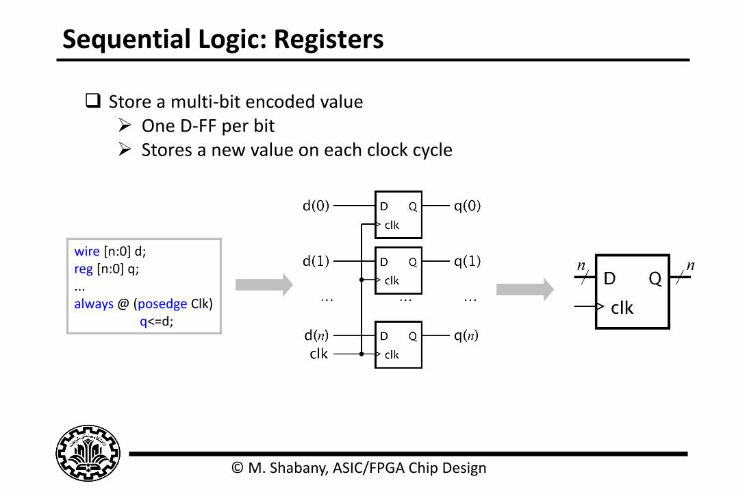
Sequential Logic: Registers
wire [n:0] d; reg [n:0] q; ... always @ (posedge Clk) q<=d;
Store a multi-bit encoded value One D-FF per bit Stores a new value on each clock cycle
© M. Shabany, ASIC/FPGA Chip Design
Reg Type (Revisited)
The keyword “reg” does NOT necessarily denote a storage element or register.
“reg” simply means a variable that can hold a value
May or may not be synthesized as a register.
reg C; always @ (a,b) C = a+b;
reg C; always @ (posedge Clk) C <= a+b;
a
b
C
Clk
a
b
C
Register Not Register
Signal
Type Range Name Value
© M. Shabany, ASIC/FPGA Chip Design
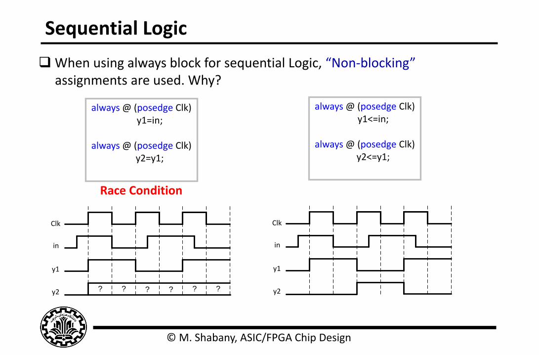
Sequential Logic
When using always block for sequential Logic, “Non-blocking” assignments are used. Why?
always @ (posedge Clk) y1=in;
always @ (posedge Clk)
y2=y1;
always @ (posedge Clk) y1<=in;
always @ (posedge Clk)
y2<=y1;
Clk
in
y1
y2 ? ? ? ? ? ?
Clk
in
y1
y2
Race Condition
© M. Shabany, ASIC/FPGA Chip Design
Sequential Logic
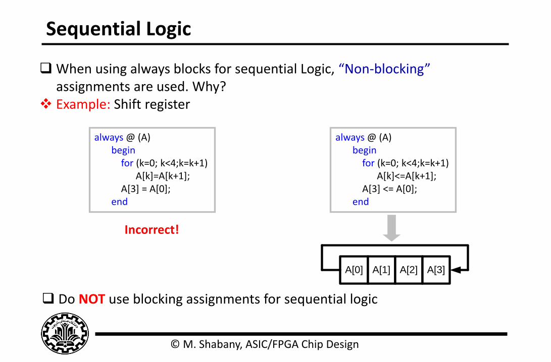
When using always blocks for sequential Logic, “Non-blocking” assignments are used. Why? Example: Shift register
always @ (A) begin for (k=0; k<4;k=k+1) A[k]=A[k+1]; A[3] = A[0]; end
always @ (A) begin for (k=0; k<4;k=k+1) A[k]<=A[k+1]; A[3] <= A[0]; end
A[0] A[1] A[2] A[3]
Incorrect!
Do NOT use blocking assignments for sequential logic
© M. Shabany, ASIC/FPGA Chip Design
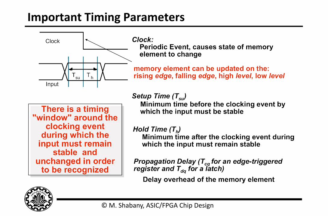
Important Timing Parameters
© M. Shabany, ASIC/FPGA Chip Design
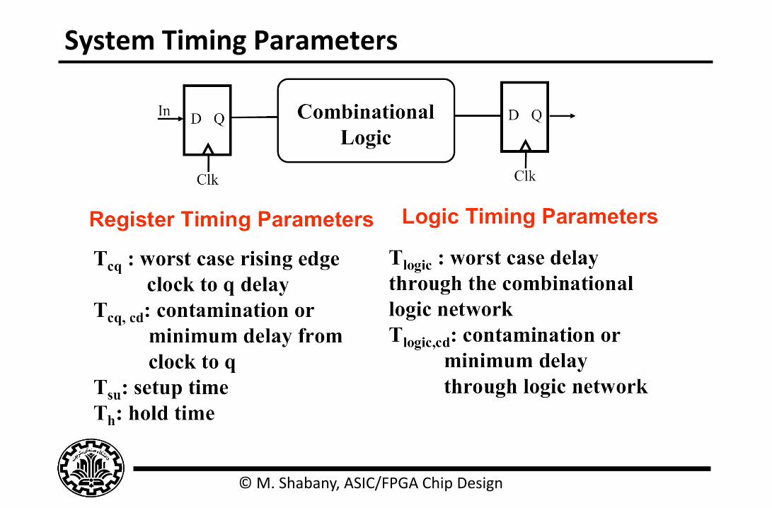
System Timing Parameters
© M. Shabany, ASIC/FPGA Chip Design
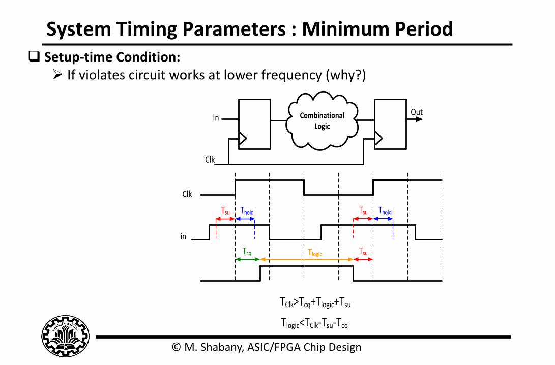
System Timing Parameters : Minimum Period Setup-time Condition:
If violates circuit works at lower frequency (why?)
Clk
in
Tsu Thold Tsu Thold
Tcq Tlogic Tsu
TClk>Tcq+Tlogic+Tsu
Tlogic<TClk-Tsu-Tcq
CombinationalLogic
Clk
InOut
© M. Shabany, ASIC/FPGA Chip Design
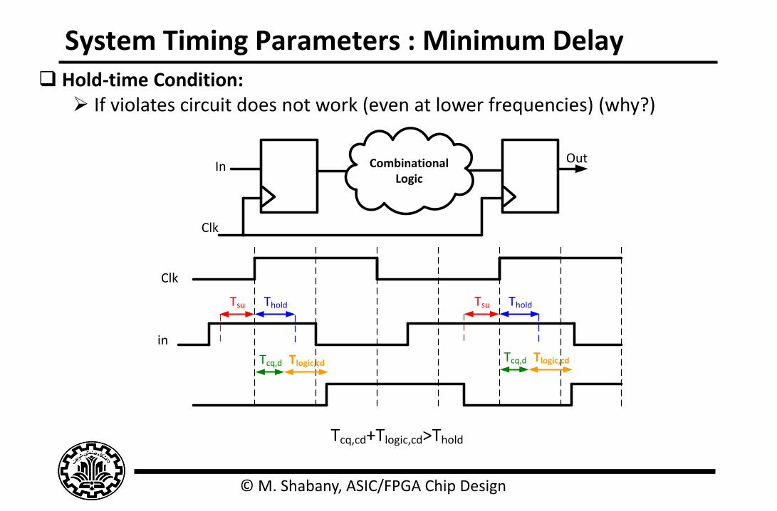
System Timing Parameters : Minimum Delay Hold-time Condition:
If violates circuit does not work (even at lower frequencies) (why?)
Clk
in
Tsu Thold Tsu Thold
Tcq,d Tlogic,cd
Tcq,cd+Tlogic,cd>Thold
CombinationalLogic
Clk
InOut
Tcq,d Tlogic,cd

© M. Shabany, ASIC/FPGA Chip Design
Procedural Statements
always @ (sensitivity list) begin
Procedural assignments if-else statements case statements while, repeat, for loops
end
Procedural Statements
Procedural Statements
Procedural Assignments If-else
Statements
Case
Statements
while repeat for
Loop statements
Blocking Non-blocking

© M. Shabany, ASIC/FPGA Chip Design
If-else statements
Used only inside an always block
Format:
Example:
If (expression1) statement1; else if (expression2) statement2; else statement3;
Single statement no need for begin-end Multiple statements, begin-end is needed
module Mux21 (in1, in2, s, out) input in1, in2, s; output reg out; always @ (in1, in2, s) if (s==0)
out = in1; else out = in2;
endmodule
in1
s
out
0
1in2
module Mux21 (in1, in2, s, out) input in1, in2, s; output reg out; always @ (in1, in2, s) begin out = in1; if (s==1)
out = in2; end
endmodule
© M. Shabany, ASIC/FPGA Chip Design
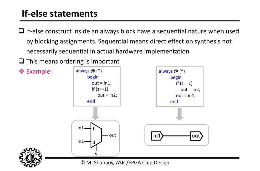
If-else statements
If-else construct inside an always block have a sequential nature when used
by blocking assignments. Sequential means direct effect on synthesis not
necessarily sequential in actual hardware implementation
This means ordering is important
Example:
in1
s
out
0
1in2
always @ (*) begin out = in1; if (s==1)
out = in2; end
always @ (*) begin if (s==1)
out = in2; out = in1;
end
in1 out
© M. Shabany, ASIC/FPGA Chip Design
Procedural Statements
always @ (sensitivity list) begin
Procedural assignments if-else statements case statements while, repeat, for loops
end
Procedural Statements
Procedural Statements
Procedural Assignments If-else
Statements
Case
Statements
while repeat for
Loop statements
Blocking Non-blocking

© M. Shabany, ASIC/FPGA Chip Design
Case statements
Used only inside an always block
Format:
Example:
case (expression) alternative1: statement1; alternative2: begin statement2; end default: statementn; endcase
Single statement no need for begin-end
module Mux21 (in1, in2, s, out) input in1, in2, s; output reg out; always @ (in1, in2, s) case (s)
1’b0: out = in1; 1’b1: out = in2; endcase
endmodule
Multiple statements, begin-end is needed
module Mux21 (in1, in2, s, out) input in1, in2, s; output reg out; always @ (in1, in2, s) case (s)
1’b0: out = in1; default: out = in2; endcase
endmodule
© M. Shabany, ASIC/FPGA Chip Design
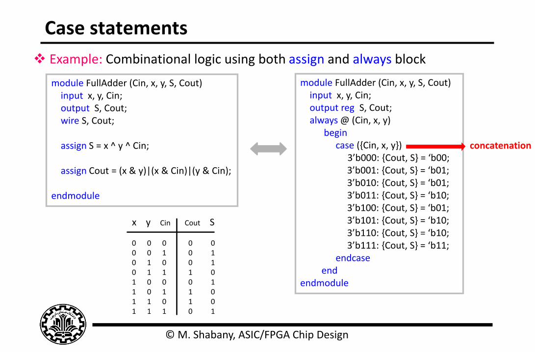
Case statements
Example: Combinational logic using both assign and always block
module FullAdder (Cin, x, y, S, Cout) input x, y, Cin; output S, Cout; wire S, Cout; assign S = x ^ y ^ Cin; assign Cout = (x & y)|(x & Cin)|(y & Cin); endmodule
module FullAdder (Cin, x, y, S, Cout) input x, y, Cin; output reg S, Cout; always @ (Cin, x, y) begin case ({Cin, x, y}) 3’b000: {Cout, S} = ‘b00; 3’b001: {Cout, S} = ‘b01; 3’b010: {Cout, S} = ‘b01; 3’b011: {Cout, S} = ‘b10; 3’b100: {Cout, S} = ‘b01; 3’b101: {Cout, S} = ‘b10; 3’b110: {Cout, S} = ‘b10; 3’b111: {Cout, S} = ‘b11; endcase end endmodule
concatenation
x y Cin Cout S
0 0 0 0 0 0 0 1 0 1 0 1 0 0 1 0 1 1 1 0 1 0 0 0 1 1 0 1 1 01 1 0 1 0 1 1 1 0 1
© M. Shabany, ASIC/FPGA Chip Design
Case statements
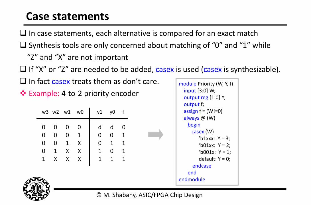
In case statements, each alternative is compared for an exact match
Synthesis tools are only concerned about matching of “0” and “1” while
“Z” and “X” are not important
If “X” or “Z” are needed to be added, casex is used (casex is synthesizable).
In fact casex treats them as don’t care.
Example: 4-to-2 priority encoder
module Priority (W, Y, f) input [3:0] W; output reg [1:0] Y; output f; assign f = (W!=0) always @ (W) begin casex (W)
’b1xxx: Y = 3; ‘b01xx: Y = 2; ‘b001x: Y = 1; default: Y = 0; endcase
end endmodule
w3 w2 w1 w0 y1 y0 f
0 0 0 0 d d 0 0 0 0 1 0 0 1 0 0 1 X 0 1 1 0 1 X X 1 0 1 1 X X X 1 1 1
© M. Shabany, ASIC/FPGA Chip Design
Case statements
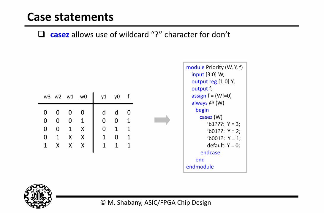
casez allows use of wildcard “?” character for don’t
module Priority (W, Y, f) input [3:0] W; output reg [1:0] Y; output f; assign f = (W!=0) always @ (W) begin casez (W)
’b1???: Y = 3; ‘b01??: Y = 2; ‘b001?: Y = 1; default: Y = 0; endcase
end endmodule
w3 w2 w1 w0 y1 y0 f
0 0 0 0 d d 0 0 0 0 1 0 0 1 0 0 1 X 0 1 1 0 1 X X 1 0 1 1 X X X 1 1 1

© M. Shabany, ASIC/FPGA Chip Design
Latch Inference in Combinational Logic
When realizing combinational logic with always block using if-else or case
constructs care has to be taken to avoid latch inference after synthesis
The latch is inferred when “incomplete” if-else or case statements are declared
This latch is “unwanted” as the logic is combinational not sequential
If there is some logic path through the always block that does not assign a value
to the output, a latch is inferred
© M. Shabany, ASIC/FPGA Chip Design
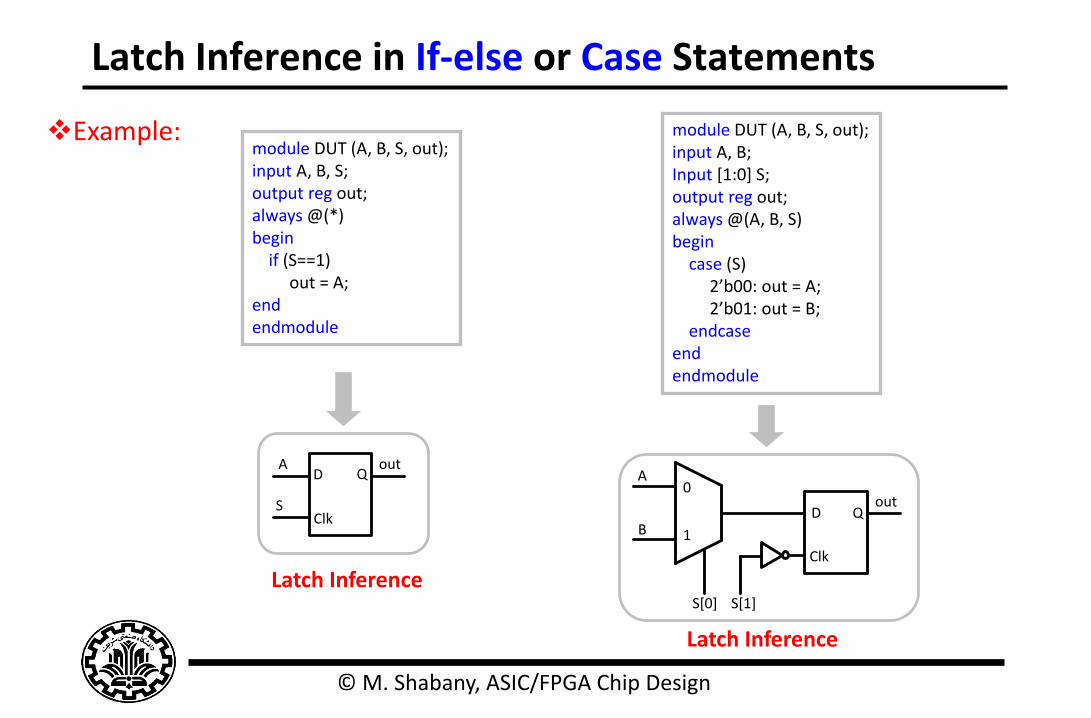
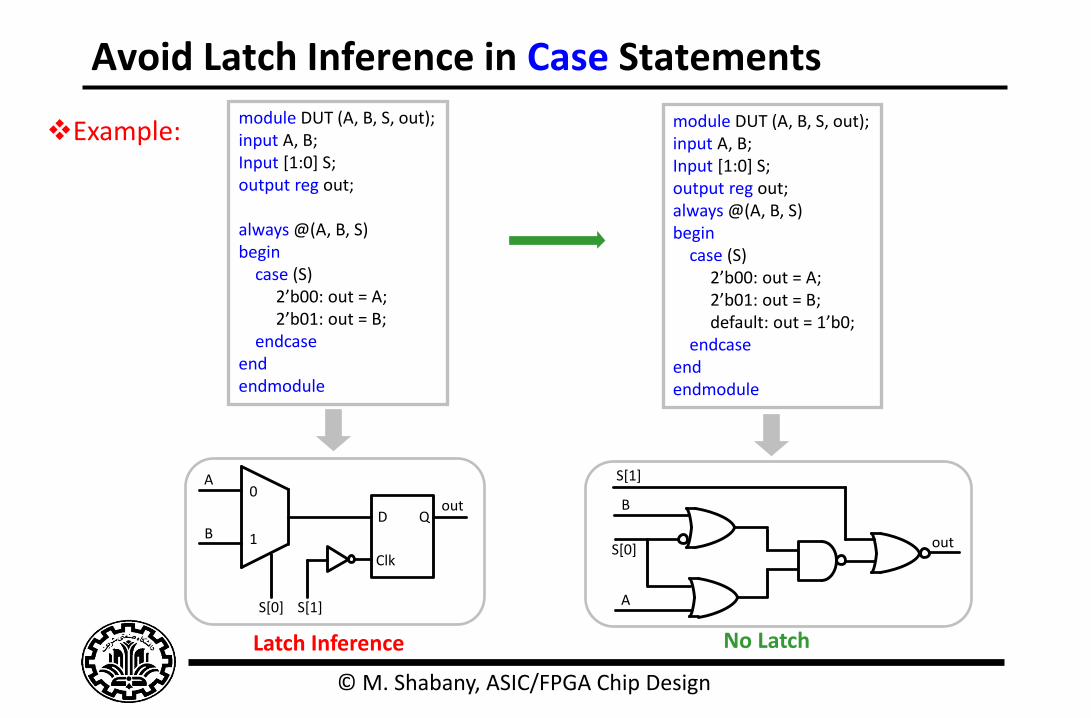
Latch Inference in If-else or Case Statements
Example:
module DUT (A, B, S, out); input A, B, S; output reg out; always @(*) begin if (S==1) out = A; end endmodule
Latch Inference
outA
S
Q
Clk
D
module DUT (A, B, S, out); input A, B; Input [1:0] S; output reg out; always @(A, B, S) begin case (S) 2’b00: out = A; 2’b01: out = B; endcase end endmodule
Latch Inference
outQ
Clk
A
B
S[0]
0
1
S[1]
D

© M. Shabany, ASIC/FPGA Chip Design
Latch Inference in Combinational Logic
To avoid latch inference make sure to specify all possible cases “explicitly”
Two practical approaches to avoid latch inference:
For if-else construct:
1. Initialize the variable before the if-else construct
2. Use else to explicitly list all possible cases
For case constructs:
1. Use default to make sure no case is missed!
Do NOT let it up to the synthesis tool to act in unspecified cases and do specify
all cases explicitly.
© M. Shabany, ASIC/FPGA Chip Design
Avoid Latch Inference in If-else Statements
Example:
module DUT (A, B, S, out); input A, B, S; output reg out; always @(*) begin if (S==1) out = A; else out =B; end endmodule
module DUT (A, B, S, out); input A, B, S; output reg out; always @(*) begin if (S==1) out = A; end endmodule
module DUT (A, B, S, out); input A, B, S; output reg out; always @(*) Begin out = B; if (S==1) out = A; end endmodule
B
S
A
out
B
S
A
out
1
2
Latch Inference
No Latch
No Latch
outA
S
Q
Clk
D
© M. Shabany, ASIC/FPGA Chip Design
Avoid Latch Inference in Case Statements
Example:
module DUT (A, B, S, out); input A, B; Input [1:0] S; output reg out; always @(A, B, S) begin case (S) 2’b00: out = A; 2’b01: out = B; endcase end endmodule
module DUT (A, B, S, out); input A, B; Input [1:0] S; output reg out; always @(A, B, S) begin case (S) 2’b00: out = A; 2’b01: out = B; default: out = 1’b0; endcase end endmodule
B
S[0]
A
out
S[1]
Latch Inference No Latch
outQ
Clk
A
B
S[0]
0
1
S[1]
D
© M. Shabany, ASIC/FPGA Chip Design
Procedural Statements
always @ (sensitivity list) begin
Procedural assignments if-else statements case statements while, repeat, for loops
end
Procedural Statements
Procedural Statements
Procedural Assignments If-else
Statements
Case
Statements
while repeat for
Loop statements
Blocking Non-blocking
© M. Shabany, ASIC/FPGA Chip Design
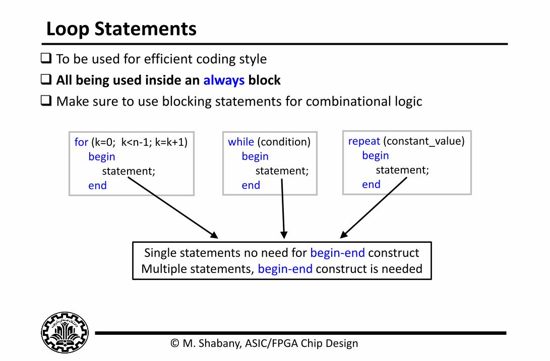
Loop Statements
To be used for efficient coding style
All being used inside an always block
Make sure to use blocking statements for combinational logic
for (k=0; k<n-1; k=k+1) begin statement; end
while (condition) begin statement; end
repeat (constant_value) begin statement; end
Single statements no need for begin-end construct Multiple statements, begin-end construct is needed

© M. Shabany, ASIC/FPGA Chip Design
Loop Statements
Example: Remember: 1-bit full Adder
module Full_Adder (Cin, x, y, S, Cout) input x, y, Cin; output S, Cout; wire S, Cout; assign S = x ^ y ^ Cin; assign Cout = (x & y)|(x & Cin)|(y & Cin); endmodule
S
y
Cin
x
Cout
© M. Shabany, ASIC/FPGA Chip Design
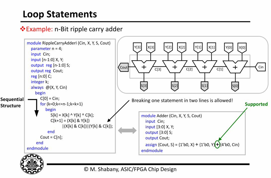
Loop Statements
Example: n-Bit ripple carry adder
module RippleCarryAdderI (Cin, X, Y, S, Cout) parameter n = 4; input Cin; input [n-1:0] X, Y; output reg [n-1:0] S; output reg Cout; reg [n:0] C; integer k; always @(X, Y, Cin) begin C[0] = Cin; for (k=0;k<=n-1;k=k+1) begin S[k] = X[k] ^ Y[k] ^ C[k]; C[k+1] = (X[k] & Y[k]) |(X[k] & C[k])|(Y[k] & C[k]); end Cout = C[n]; end endmodule
X[0]
S[0]
Y[0]
Cin
X[1]
S[1]
Y[1]X[2]
S[2]
Y[2]X[3]
S[3]
Y[3]
C[1]C[2]C[3]Cout
Breaking one statement in two lines is allowed!
module Adder (Cin, X, Y, S, Cout) input Cin; input [3:0] X, Y; output [3:0] S; output Cout;
assign {Cout, S} = {1’b0, X} + {1’b0, Y} + {4’b0, Cin}
endmodule
Supported Sequential Structure
© M. Shabany, ASIC/FPGA Chip Design
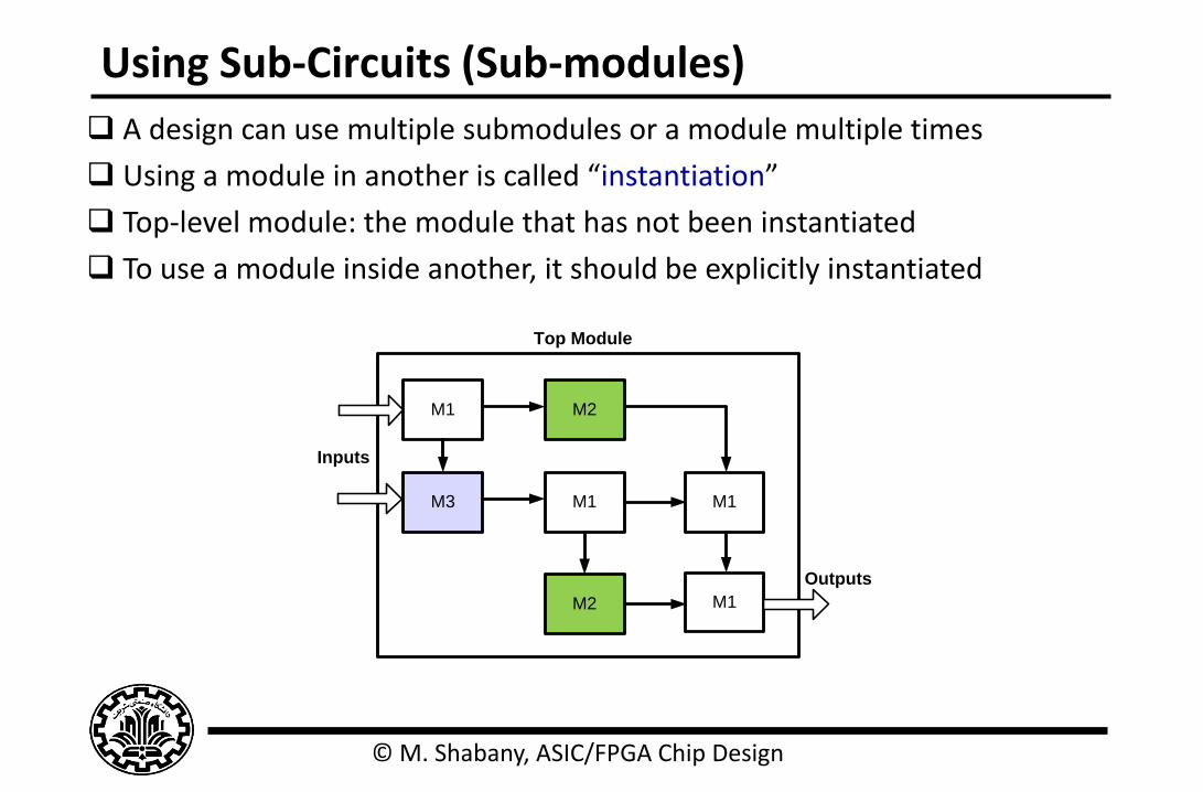
Using Sub-Circuits (Sub-modules)
A design can use multiple submodules or a module multiple times
Using a module in another is called “instantiation”
Top-level module: the module that has not been instantiated
To use a module inside another, it should be explicitly instantiated
M1 M2
M3 M1 M1
M2 M1
Top Module
Inputs
Outputs
© M. Shabany, ASIC/FPGA Chip Design
Using Sub-modules
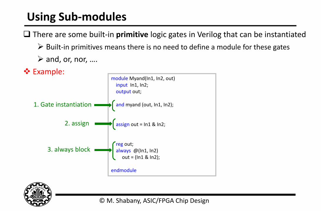
There are some built-in primitive logic gates in Verilog that can be instantiated
Built-in primitives means there is no need to define a module for these gates
and, or, nor, ….
Example: module Myand(In1, In2, out) input In1, In2; output out; and myand (out, In1, In2); assign out = In1 & In2; reg out; always @(In1, In2) out = (In1 & In2); endmodule
3. always block
2. assign
1. Gate instantiation
© M. Shabany, ASIC/FPGA Chip Design
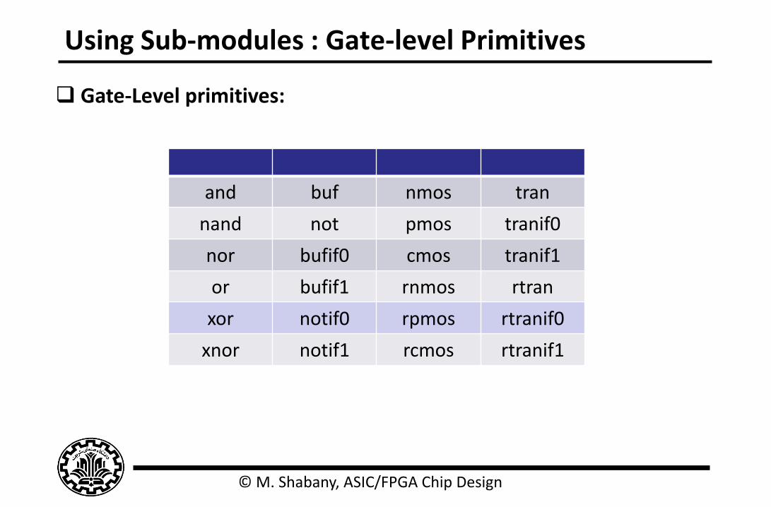
Using Sub-modules : Gate-level Primitives
and buf nmos tran
nand not pmos tranif0
nor bufif0 cmos tranif1
or bufif1 rnmos rtran
xor notif0 rpmos rtranif0
xnor notif1 rcmos rtranif1
Gate-Level primitives:
© M. Shabany, ASIC/FPGA Chip Design
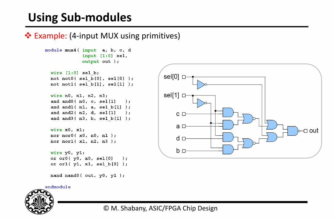
Using Sub-modules
Example: (4-input MUX using primitives)
© M. Shabany, ASIC/FPGA Chip Design
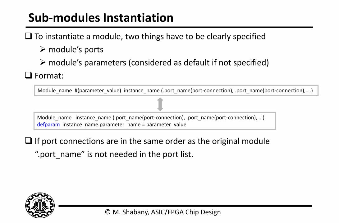
Sub-modules Instantiation
To instantiate a module, two things have to be clearly specified
module’s ports
module’s parameters (considered as default if not specified)
Format:
If port connections are in the same order as the original module
“.port_name” is not needed in the port list.
Module_name #(parameter_value) instance_name (.port_name(port-connection), .port_name(port-connection),….)
Module_name instance_name (.port_name(port-connection), .port_name(port-connection),….) defparam instance_name.parameter_name = parameter_value
© M. Shabany, ASIC/FPGA Chip Design
Sub-modules Instantiation
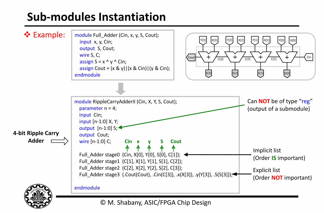
Example:
module RippleCarryAdderII (Cin, X, Y, S, Cout); parameter n = 4; input Cin; input [n-1:0] X, Y; output [n-1:0] S; output Cout; wire [n-1:0] C; Cin x y S Cout Full_Adder stage0 (Cin, X[0], Y[0], S[0], C[1]); Full_Adder stage1 (C[1], X[1], Y[1], S[1], C[2]); Full_Adder stage2 (C[2], X[2], Y[2], S[2], C[3]); Full_Adder stage3 (.Cout(Cout), .Cin(C[3]), .x(X[3]), .y(Y[3]), .S(S[3])); endmodule
module Full_Adder (Cin, x, y, S, Cout); input x, y, Cin; output S, Cout; wire S, C; assign S = x ^ y ^ Cin; assign Cout = (x & y)|(x & Cin)|(y & Cin); endmodule
Explicit list (Order NOT important)
Implicit list (Order IS important)
4-bit Ripple Carry Adder
Can NOT be of type “reg” (output of a submodule)
X[0]
S[0]
Y[0]
Cin
X[1]
S[1]
Y[1]X[2]
S[2]
Y[2]X[3]
S[3]
Y[3]
C[1]C[2]C[3]Cout
© M. Shabany, ASIC/FPGA Chip Design
Sub-modules Instantiation
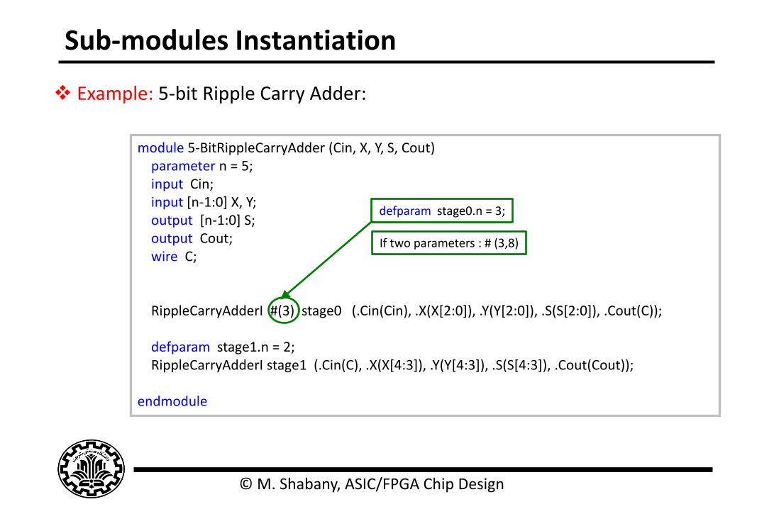
Example: 5-bit Ripple Carry Adder:
module 5-BitRippleCarryAdder (Cin, X, Y, S, Cout) parameter n = 5; input Cin; input [n-1:0] X, Y; output [n-1:0] S; output Cout; wire C; RippleCarryAdderI #(3) stage0 (.Cin(Cin), .X(X[2:0]), .Y(Y[2:0]), .S(S[2:0]), .Cout(C)); defparam stage1.n = 2; RippleCarryAdderI stage1 (.Cin(C), .X(X[4:3]), .Y(Y[4:3]), .S(S[4:3]), .Cout(Cout)); endmodule
defparam stage0.n = 3;
If two parameters : # (3,8)

© M. Shabany, ASIC/FPGA Chip Design
Sub-modules Instantiation
Example:
M1Parameter length =10;
in1
in2
out1
out2
module DUT (IN, OUT) input [2:0] IN; output [2:0] OUT; wire w1, w2, w3; defparam stage0.length = 6; M1 stage0 (IN[0], IN[1], w1, w2); defparam stage1.length = 3; M1 stage1 (.in1(w1), .in2(IN[2]), .out2(w3), .out1(OUT[2])); M1 stage2 (.in1(w2), .in2(w3), .out1(OUT[0]), .out2(OUT[1])); endmodule
M1
(6)
M1
(10)
DUT
IN_0
IN_1
w1
w2
w3
OUT_0
M1
(3)
IN_2
OUT_1
OUT_2
© M. Shabany, ASIC/FPGA Chip Design
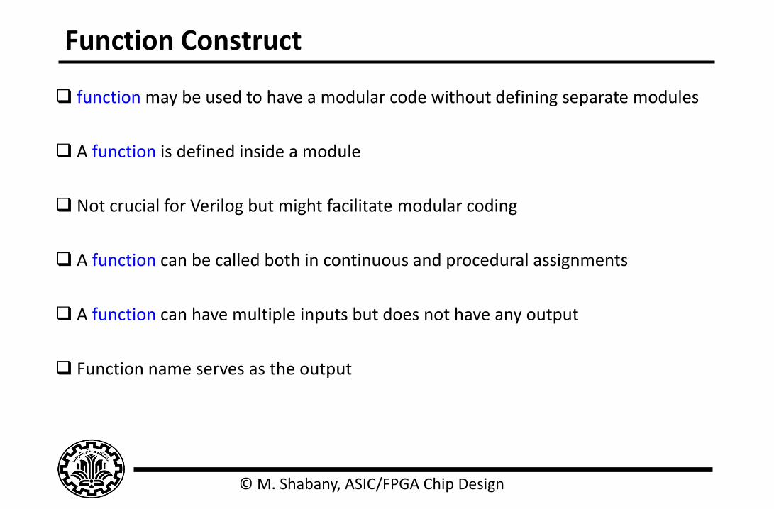
Function Construct
function may be used to have a modular code without defining separate modules
A function is defined inside a module
Not crucial for Verilog but might facilitate modular coding
A function can be called both in continuous and procedural assignments
A function can have multiple inputs but does not have any output
Function name serves as the output
© M. Shabany, ASIC/FPGA Chip Design
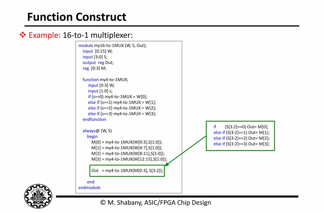
Function Construct
Example: 16-to-1 multiplexer:
module my16-to-1MUX (W, S, Out); input [0:15] W; input [3:0] S; output reg Out; reg [0:3] M; function my4-to-1MUX; input [0:3] W; input [1:0] s; if (s==0) my4-to-1MUX = W[0]; else if (s==1) my4-to-1MUX = W[1]; else if (s==2) my4-to-1MUX = W[2]; else if (s==3) my4-to-1MUX = W[3]; endfunction always@ (W, S) begin M[0] = my4-to-1MUX(W[0:3],S[1:0]); M[1] = my4-to-1MUX(W[4:7],S[1:0]); M[2] = my4-to-1MUX(W[8:11],S[1:0]); M[3] = my4-to-1MUX(W[12:15],S[1:0]); Out = my4-to-1MUX(M[0:3], S[3:2]); end endmodule
if (S[3:2]==0) Out= M[0]; else if (S[3:2]==1) Out= M[1]; else if (S[3:2]==2) Out= M[2]; else if (S[3:2]==3) Out= M[3];

© M. Shabany, ASIC/FPGA Chip Design
Function Construct with multiple-bit output
Example:
module test_fcn (a, b, c, Out); input a, b, c; output reg [2:0] Out; function [2:0] myfcn; input a, b, c; begin myfcn[0] = a^b; myfcn[1] = b^c; myfcn[2] = c^a; end endfunction always @(*) Out = myfcn(a,b,c); endmodule
module test_fcn (a, b, c, Out); input a, b, c; output [2:0] Out; function [2:0] myfcn; input a, b, c; begin myfcn[0] = a^b; myfcn[1] = b^c; myfcn[2] = c^a; end endfunction assign Out = myfcn(a,b,c); endmodule
With always With assign
© M. Shabany, ASIC/FPGA Chip Design
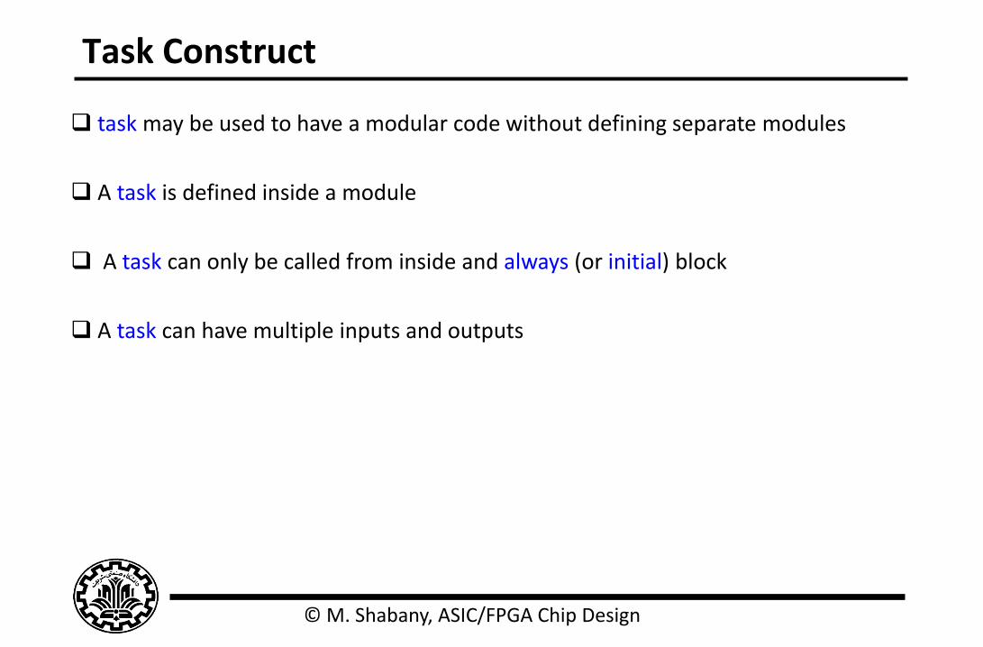
Task Construct
task may be used to have a modular code without defining separate modules
A task is defined inside a module
A task can only be called from inside and always (or initial) block
A task can have multiple inputs and outputs
© M. Shabany, ASIC/FPGA Chip Design
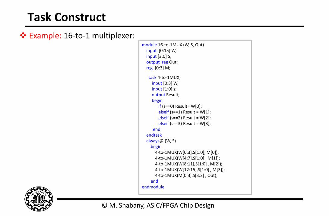
Task Construct
Example: 16-to-1 multiplexer:
module 16-to-1MUX (W, S, Out) input [0:15] W; input [3:0] S; output reg Out; reg [0:3] M;
task 4-to-1MUX; input [0:3] W; input [1:0] s; output Result; begin if (s==0) Result= W[0]; elseif (s==1) Result = W[1]; elseif (s==2) Result = W[2]; elseif (s==3) Result = W[3]; end endtask always@ (W, S) begin 4-to-1MUX(W[0:3],S[1:0], M[0]); 4-to-1MUX(W[4:7],S[1:0] , M[1]); 4-to-1MUX(W[8:11],S[1:0] , M[2]); 4-to-1MUX(W[12:15],S[1:0] , M[3]); 4-to-1MUX(M[0:3],S[3:2] , Out); end endmodule

© M. Shabany, ASIC/FPGA Chip Design
HDL for Synthesis (Priority logic)
The order in which assignments are written in an always block may affect the logic
that is synthesized. (both conditions in if and else if can be true!)
Example:
always @ (s0,s1, d0, d1) begin Q = 0; if (s0) Q = d0; else if (s1) Q = d1; end
0
d1
s1
0
1
d0
s0
0
1
Q
Different
Non of the above infer latch, why?
always @ (s0,s1, d0, d1) begin Q = 0; if (s1) Q = d1; else if (s0) Q = d0; end
0
d0
s0
0
1
d1
s1
0
1
Q
© M. Shabany, ASIC/FPGA Chip Design
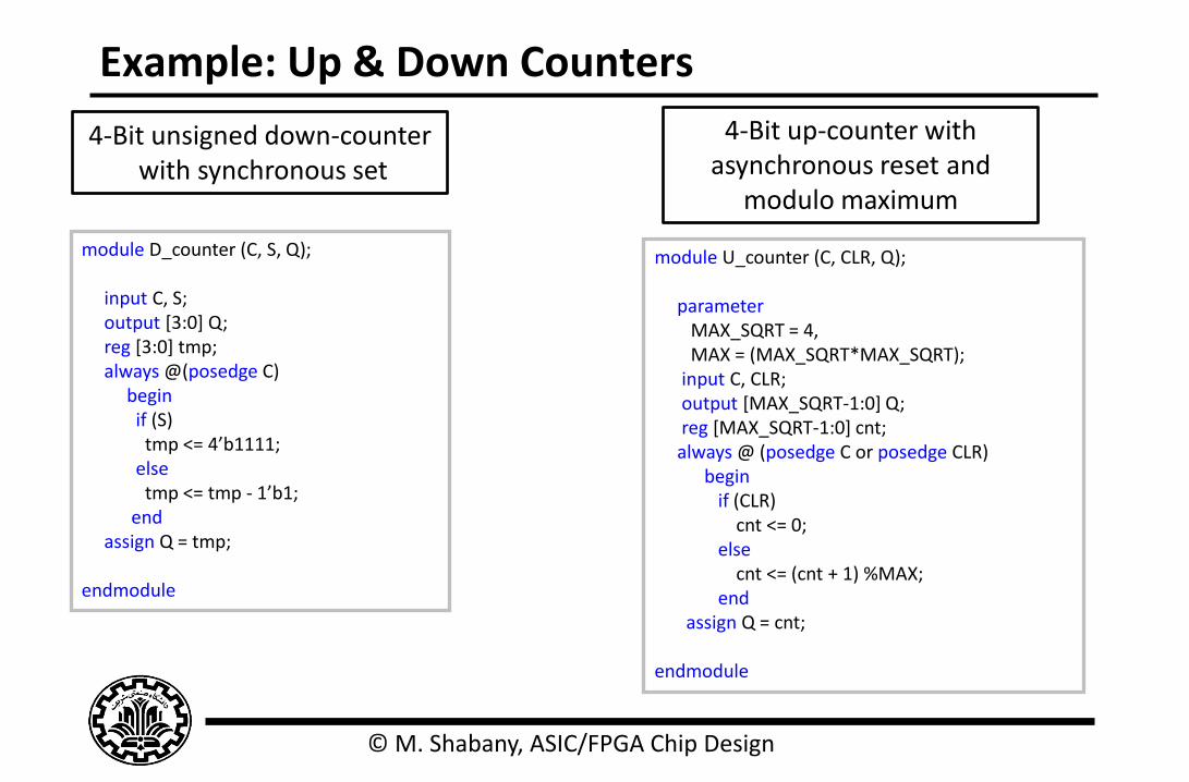
Example: Up & Down Counters
4-Bit unsigned down-counter with synchronous set
module D_counter (C, S, Q); input C, S; output [3:0] Q; reg [3:0] tmp; always @(posedge C) begin if (S) tmp <= 4’b1111; else tmp <= tmp - 1’b1; end assign Q = tmp; endmodule
4-Bit up-counter with asynchronous reset and
modulo maximum
module U_counter (C, CLR, Q); parameter MAX_SQRT = 4, MAX = (MAX_SQRT*MAX_SQRT); input C, CLR; output [MAX_SQRT-1:0] Q; reg [MAX_SQRT-1:0] cnt; always @ (posedge C or posedge CLR) begin if (CLR) cnt <= 0; else cnt <= (cnt + 1) %MAX; end assign Q = cnt; endmodule
© M. Shabany, ASIC/FPGA Chip Design
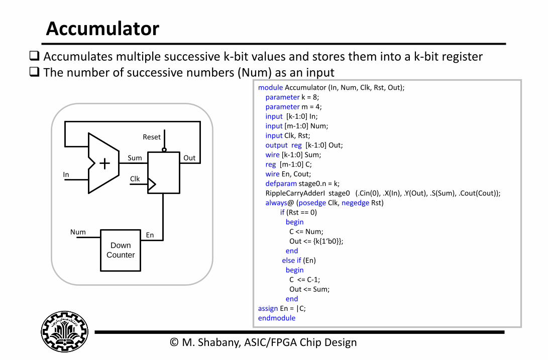
Accumulator Accumulates multiple successive k-bit values and stores them into a k-bit register The number of successive numbers (Num) as an input
module Accumulator (In, Num, Clk, Rst, Out); parameter k = 8; parameter m = 4; input [k-1:0] In; input [m-1:0] Num; input Clk, Rst; output reg [k-1:0] Out; wire [k-1:0] Sum; reg [m-1:0] C; wire En, Cout; defparam stage0.n = k; RippleCarryAdderI stage0 (.Cin(0), .X(In), .Y(Out), .S(Sum), .Cout(Cout)); always@ (posedge Clk, negedge Rst) if (Rst == 0) begin C <= Num; Out <= {k{1‘b0}}; end else if (En) begin C <= C-1; Out <= Sum; end assign En = |C; endmodule
Clk
Sum Out
Reset
In
Down
Counter
Num En
© M. Shabany, ASIC/FPGA Chip Design
Outline
ASIC/FPGA Design Flow
Hardware Description Language (HDL)
Verilog
o Introduction
o Language Fundamentals
o Modeling Combinational & Sequential Logic Circuits
o Modeling Finite State Machines
o Verilog Operations
136
© M. Shabany, ASIC/FPGA Chip Design
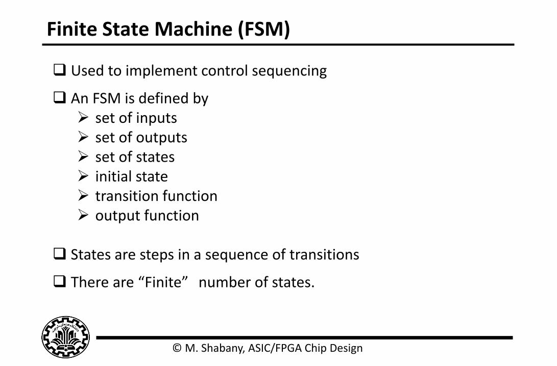
Finite State Machine (FSM)
Used to implement control sequencing
An FSM is defined by set of inputs set of outputs set of states initial state transition function output function
States are steps in a sequence of transitions
There are “Finite”‖ number of states.
© M. Shabany, ASIC/FPGA Chip Design
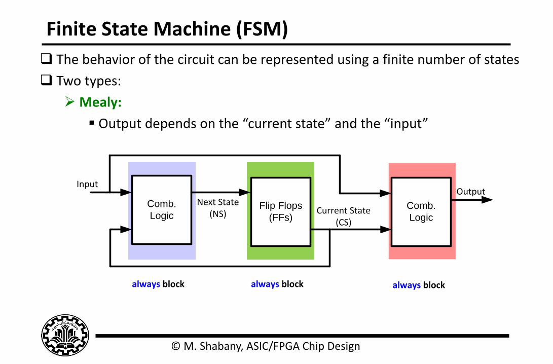
Finite State Machine (FSM)
The behavior of the circuit can be represented using a finite number of states
Two types:
Mealy:
Output depends on the “current state” and the “input”
Comb.
LogicFlip Flops
(FFs)
Comb.
Logic
Input
Next State(NS) Current State
(CS)
Output
always block always block always block
© M. Shabany, ASIC/FPGA Chip Design
Finite State Machine (FSM)
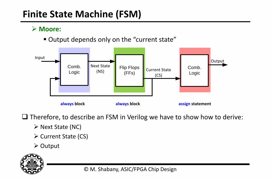
Moore:
Output depends only on the “current state”
Comb.
LogicFlip Flops
(FFs)
Comb.
Logic
Input
Next State(NS) Current State
(CS)
Output
always block always block assign statement
Therefore, to describe an FSM in Verilog we have to show how to derive:
Next State (NC)
Current State (CS)
Output
© M. Shabany, ASIC/FPGA Chip Design
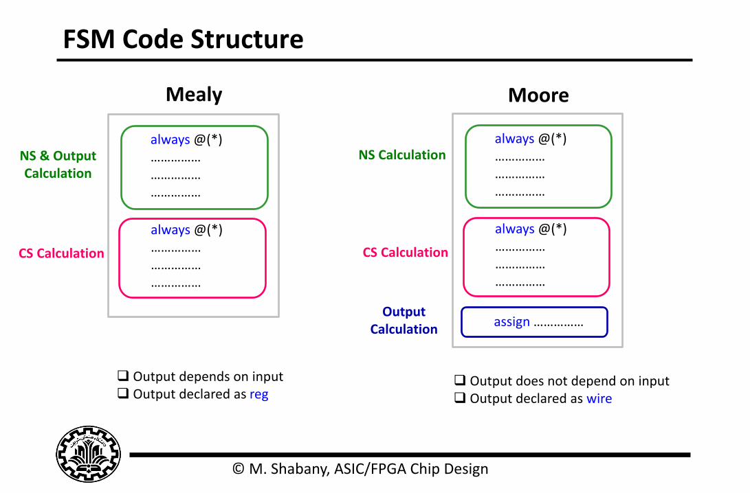
FSM Code Structure
always @(*) …………… …………… ……………
always @(*) …………… …………… ……………
NS & Output Calculation
CS Calculation
Mealy
Output depends on input Output declared as reg
always @(*) …………… …………… ……………
always @(*) …………… …………… ……………
assign ……………
NS Calculation
CS Calculation
Output Calculation
Moore
Output does not depend on input Output declared as wire
© M. Shabany, ASIC/FPGA Chip Design
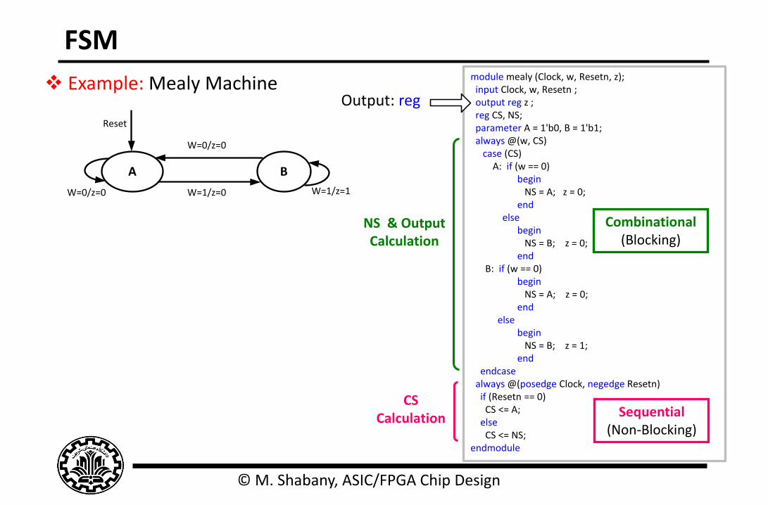
FSM module mealy (Clock, w, Resetn, z); input Clock, w, Resetn ; output reg z ; reg CS, NS; parameter A = 1'b0, B = 1'b1; always @(w, CS) case (CS) A: if (w == 0) begin NS = A; z = 0; end else begin NS = B; z = 0; end B: if (w == 0) begin NS = A; z = 0; end else begin NS = B; z = 1; end endcase always @(posedge Clock, negedge Resetn) if (Resetn == 0) CS <= A; else CS <= NS; endmodule
Example: Mealy Machine
NS & Output Calculation
CS Calculation
A B
Reset
W=1/z=0
W=0/z=0
W=1/z=1W=0/z=0
Combinational (Blocking)
Sequential (Non-Blocking)
Output: reg
© M. Shabany, ASIC/FPGA Chip Design
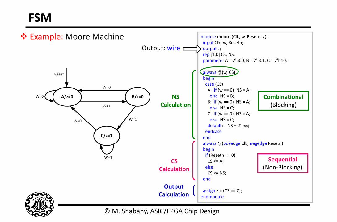
FSM
module moore (Clk, w, Resetn, z); input Clk, w, Resetn; output z; reg [1:0] CS, NS; parameter A = 2'b00, B = 2'b01, C = 2'b10; always @(w, CS) begin case (CS) A: if (w == 0) NS = A; else NS = B; B: if (w == 0) NS = A; else NS = C; C: if (w == 0) NS = A; else NS = C; default: NS = 2'bxx; endcase end always @(posedge Clk, negedge Resetn) begin if (Resetn == 0) CS <= A; else CS <= NS; end assign z = (CS == C); endmodule
Example: Moore Machine
A/z=0 B/z=0
C/z=1
Reset
W=0
W=0
W=0
W=1
W=1
W=1
NS Calculation
CS Calculation
Output Calculation
Output: wire
Combinational (Blocking)
Sequential (Non-Blocking)
© M. Shabany, ASIC/FPGA Chip Design
Outline
ASIC/FPGA Design Flow
Hardware Description Language (HDL)
Verilog
o Introduction
o Language Fundamentals
o Modeling Combinational & Sequential Logic Circuits
o Modeling Finite State Machines
o Verilog Operations
143
© M. Shabany, ASIC/FPGA Chip Design
Tri-State Logic in Verilog Tri-state buffer:
Tri-state driver inference:
module tri-buffer (A, y, EN) input A, EN; output Y; assign Y = (EN) ? A : 1’bZ; endmodule
A EN = 1 Z EN = 0
Y = Y
EN
A
always @ (ENa, a) begin if (ENa) out = a; else out = 1’bz; end always @ (ENb, b) begin if (ENb) out = b; else out = 1’bz; end
outENa
a
ENb
b
assign out = (ENa) ? a : 1’bz; assign out = (ENb) ? b : 1’bz;
© M. Shabany, ASIC/FPGA Chip Design
Tri-State Applications 1. Buffering:
2. Half-duplex communication:
3. Bus multiplexing:
Y
EN
A
Ena = 0
A
Enb = 1
Ena = 0Enb = 1
Ena = 1
A
Enb = 0
Ena = 1Enb = 0
Out[7:0]s
a
b 8
8 8
8
8
© M. Shabany, ASIC/FPGA Chip Design
Tri-State Applications Example: Adder with four options
S_ab
a
b 8
8 8
8
8
S_cd
c
d 8
8 8
8
8
Out[7:0]
p
q
module tri-adder (a, b, c, d, S_ab, S_cd, Out); input S_ab, S_cd; input [7:0] a, b, c, d; output [8:0] Out; wire [7:0] p, q; assign p = ~S_ab ? a : 8’bzzzzzzzz; assign p = S_ab ? b : 8’bzzzzzzzz; assign q = ~S_cd ? c : 8’bzzzzzzzz; assign q = S_cd ? d : 8’bzzzzzzzz; assign Out = p + q; endmodule
Z is an allowed logic value and implies a tri-state driver for synthesis

© M. Shabany, ASIC/FPGA Chip Design
Verilog Operations: Right/Left Shift
Verilog supports << for left and >> for right shift. (Only one position)
Both of these operators use a zero for the shift input bit.
We can also control the shift input
module LRShift (Si, L, R, In, Out); input Si, L, R; input [7:0] In; output [7:0] Out; always @ (L, R, In, Si) begin case({R,L}) 2’b01 : Out = {In[6:0], Si}; // Left shift 2’b10 : Out = {Si, In[7:1]}; // Right shift default: Out = In; endcase end endmodule

© M. Shabany, ASIC/FPGA Chip Design
Verilog Operations: Barrel Shifter
Barrel shifter shifts a signal by multiple positions
Example:
32-bit left shift barrel shifter
Left shifts by 0 to 31 positions based on the 5-bit s input
Each of its stages corresponds to a fixed shift by a power of 2 (16, 8, 4, 2, 1)
Simple HDL implementation, which illustrates the power of HDL to hide
implementation details from a designer
module BarrelShifter (s, a, y); input [4:0] s; input [31:0] a; output [31:0] y; assign y = a<<s; endmodule
© M. Shabany, ASIC/FPGA Chip Design
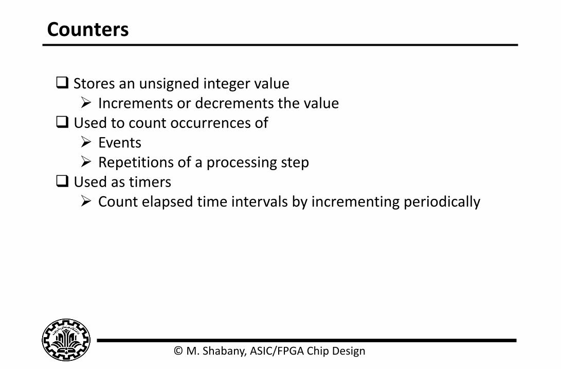
Counters
Stores an unsigned integer value Increments or decrements the value
Used to count occurrences of Events Repetitions of a processing step
Used as timers Count elapsed time intervals by incrementing periodically
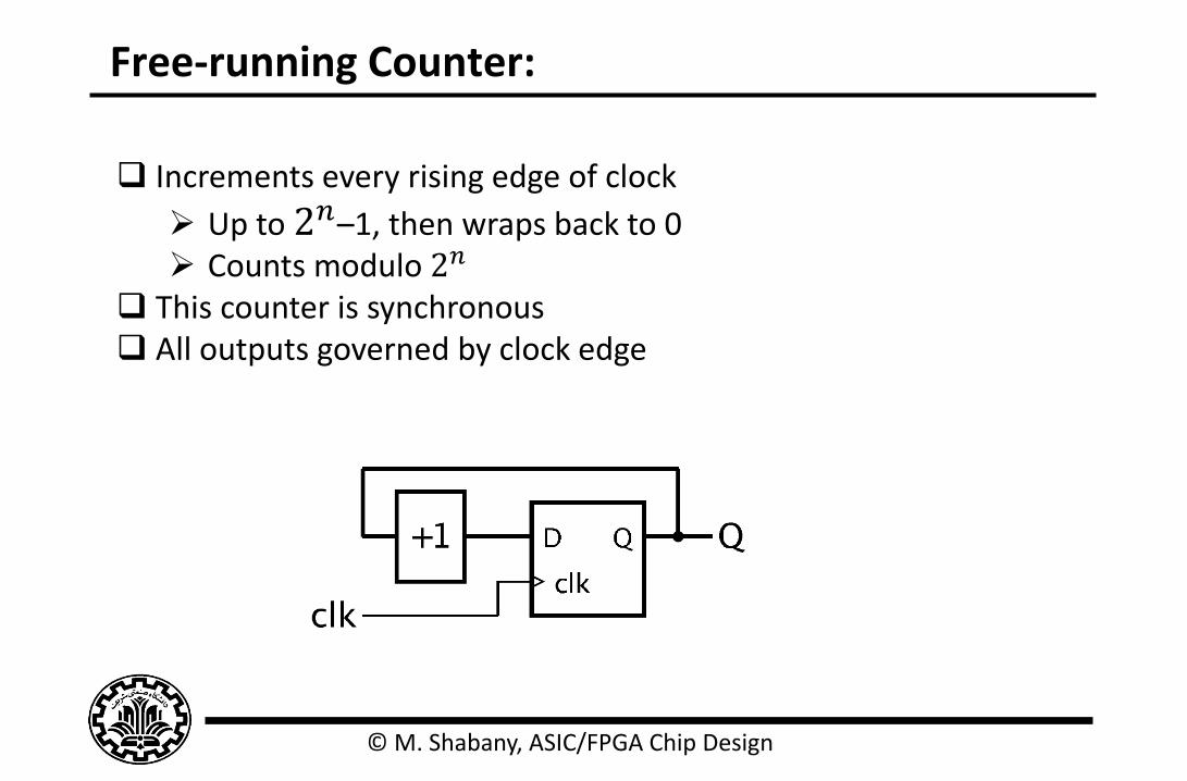
© M. Shabany, ASIC/FPGA Chip Design
Free-running Counter:
Increments every rising edge of clock
Up to 2𝑛–1, then wraps back to 0 Counts modulo 2𝑛
This counter is synchronous All outputs governed by clock edge
© M. Shabany, ASIC/FPGA Chip Design
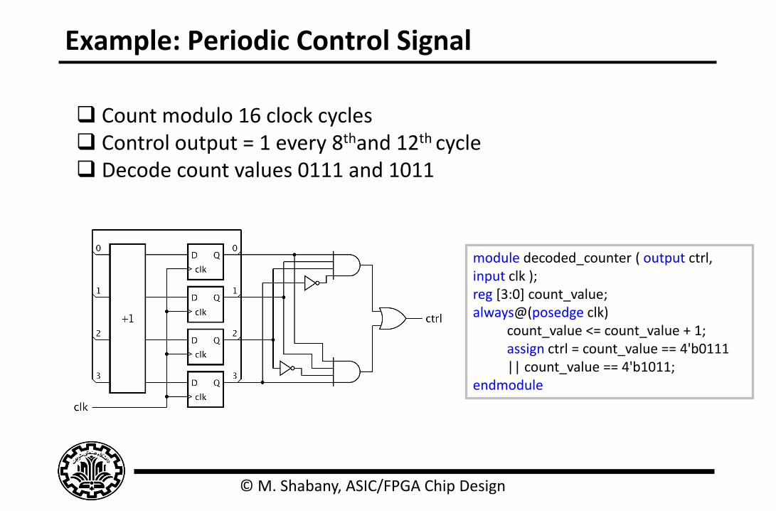
Example: Periodic Control Signal
Count modulo 16 clock cycles Control output = 1 every 8thand 12th cycle Decode count values 0111 and 1011
module decoded_counter ( output ctrl, input clk ); reg [3:0] count_value; always@(posedge clk)
count_value <= count_value + 1; assign ctrl = count_value == 4'b0111 || count_value == 4'b1011;
endmodule
© M. Shabany, ASIC/FPGA Chip Design
Fixed-point vs. Floating-point
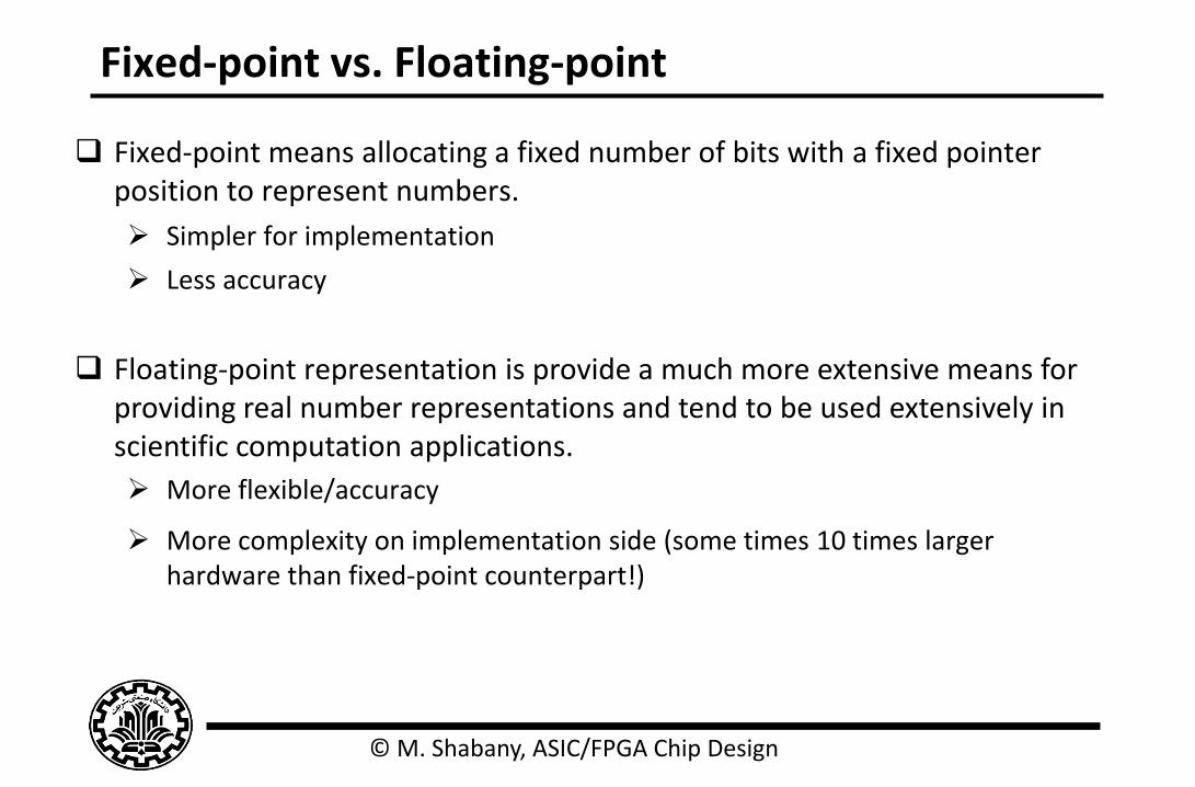
Fixed-point means allocating a fixed number of bits with a fixed pointer position to represent numbers.
Simpler for implementation
Less accuracy
Floating-point representation is provide a much more extensive means for providing real number representations and tend to be used extensively in scientific computation applications.
More flexible/accuracy
More complexity on implementation side (some times 10 times larger hardware than fixed-point counterpart!)
© M. Shabany, ASIC/FPGA Chip Design
Verilog Operations: Fixed-Point Simulation
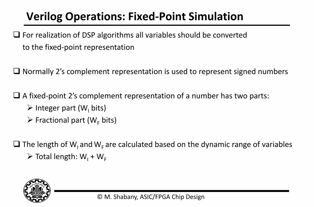
For realization of DSP algorithms all variables should be converted
to the fixed-point representation
Normally 2’s complement representation is used to represent signed numbers
A fixed-point 2’s complement representation of a number has two parts:
Integer part (WI bits)
Fractional part (WF bits)
The length of WI and WF are calculated based on the dynamic range of variables
Total length: WI + WF
© M. Shabany, ASIC/FPGA Chip Design
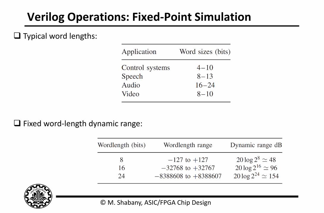
Verilog Operations: Fixed-Point Simulation
Typical word lengths:
Fixed word-length dynamic range:
© M. Shabany, ASIC/FPGA Chip Design
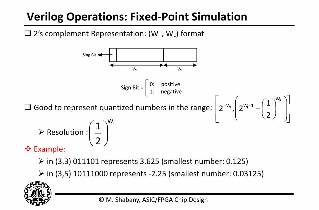
Verilog Operations: Fixed-Point Simulation
2’s complement Representation: (WI , WF) format
Good to represent quantized numbers in the range:
Resolution :
Example:
in (3,3) 011101 represents 3.625 (smallest number: 0.125)
in (3,5) 10111000 represents -2.25 (smallest number: 0.03125)
WI WF
Sign Bit = 0: positive
1: negative
Sing Bit
F
II
W
1WW
2
12,2
FW
2
1
© M. Shabany, ASIC/FPGA Chip Design
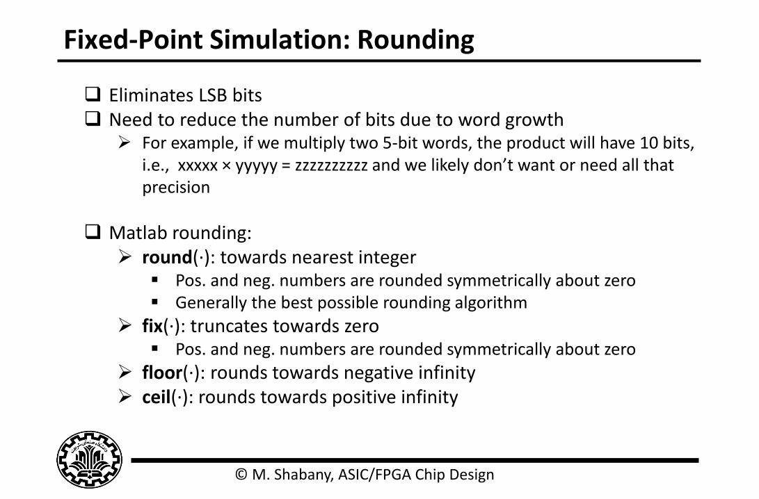
Fixed-Point Simulation: Rounding
Eliminates LSB bits Need to reduce the number of bits due to word growth
For example, if we multiply two 5‐bit words, the product will have 10 bits, i.e., xxxxx × yyyyy = zzzzzzzzzz and we likely don’t want or need all that precision
Matlab rounding: round(∙): towards nearest integer
Pos. and neg. numbers are rounded symmetrically about zero Generally the best possible rounding algorithm
fix(∙): truncates towards zero Pos. and neg. numbers are rounded symmetrically about zero
floor(∙): rounds towards negative infinity ceil(∙): rounds towards positive infinity
© M. Shabany, ASIC/FPGA Chip Design
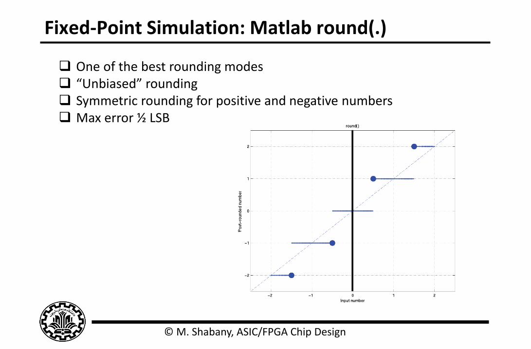
Fixed-Point Simulation: Matlab round(.)
One of the best rounding modes “Unbiased” rounding Symmetric rounding for positive and negative numbers Max error ½ LSB
© M. Shabany, ASIC/FPGA Chip Design
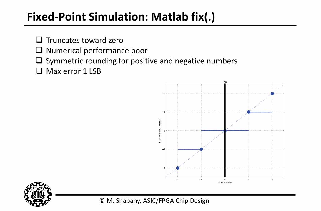
Fixed-Point Simulation: Matlab fix(.)
Truncates toward zero Numerical performance poor Symmetric rounding for positive and negative numbers Max error 1 LSB
© M. Shabany, ASIC/FPGA Chip Design
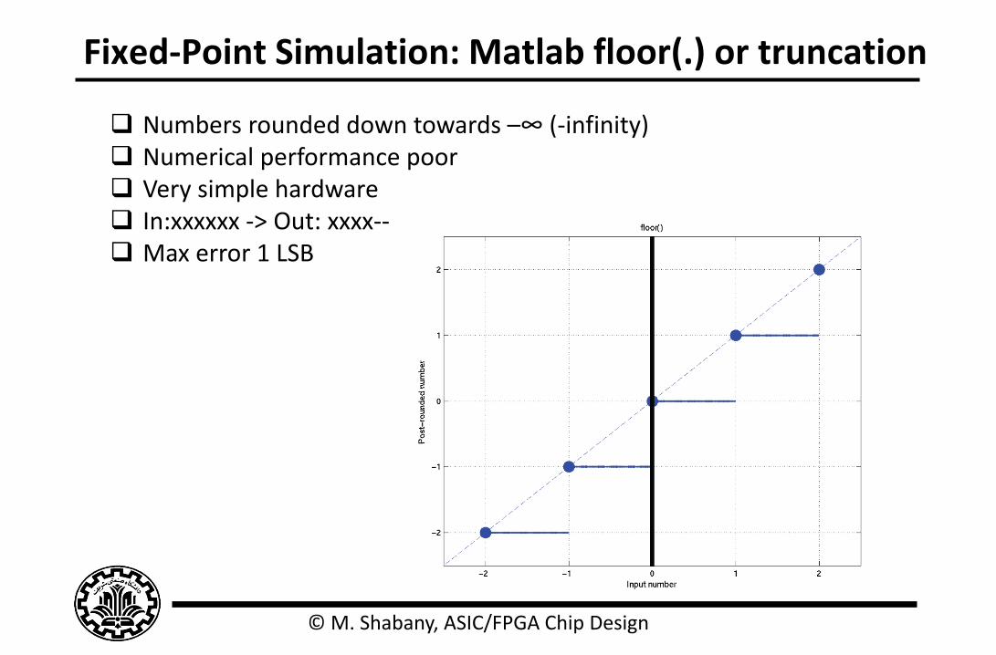
Fixed-Point Simulation: Matlab floor(.) or truncation
Numbers rounded down towards –∞ (-infinity) Numerical performance poor Very simple hardware In:xxxxxx -> Out: xxxx-- Max error 1 LSB
© M. Shabany, ASIC/FPGA Chip Design
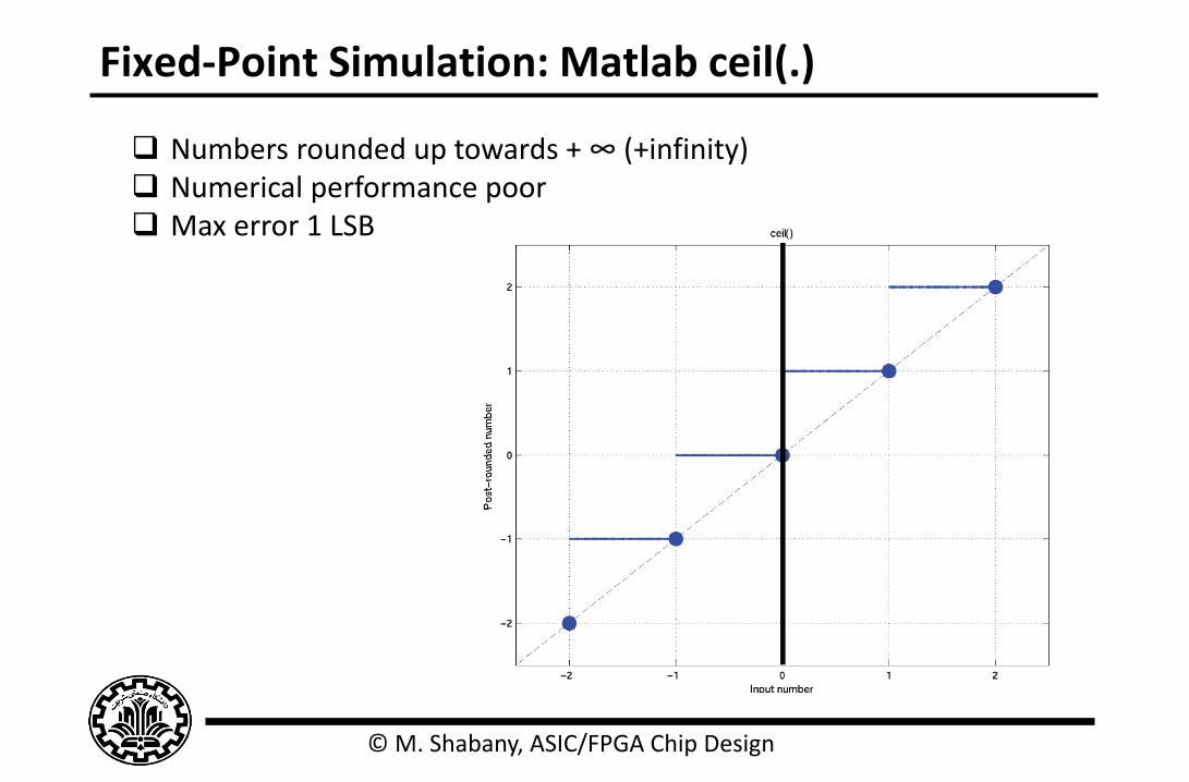
Fixed-Point Simulation: Matlab ceil(.)
Numbers rounded up towards + ∞ (+infinity) Numerical performance poor Max error 1 LSB
© M. Shabany, ASIC/FPGA Chip Design
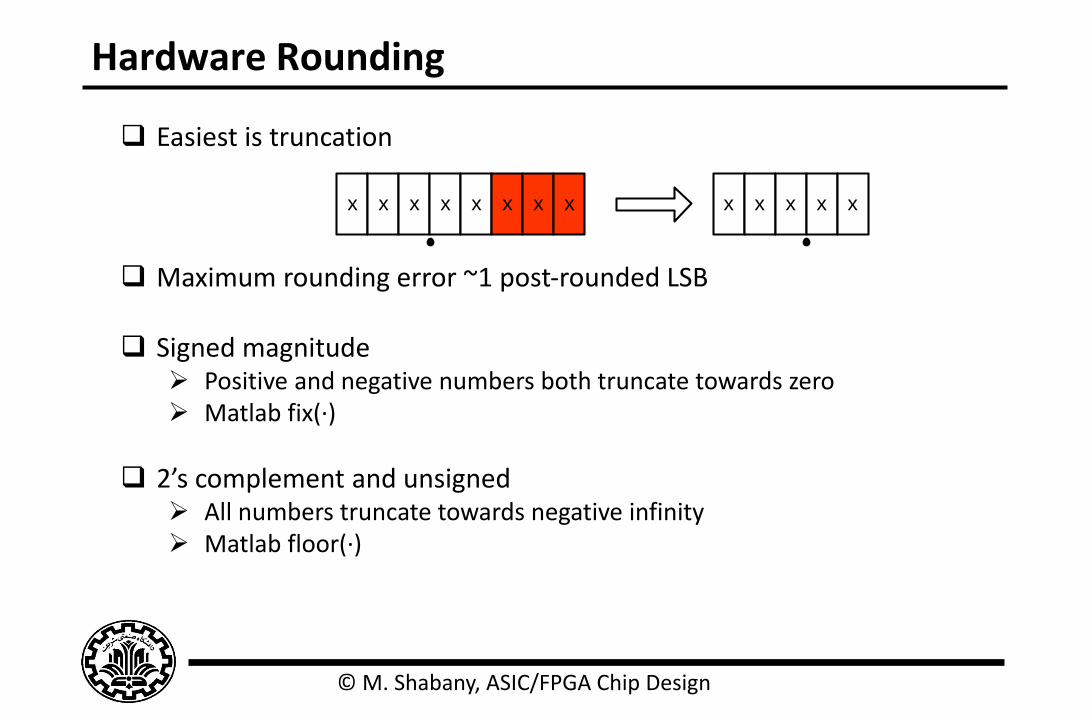
Hardware Rounding
Easiest is truncation
Maximum rounding error ~1 post‐rounded LSB
Signed magnitude Positive and negative numbers both truncate towards zero Matlab fix(∙)
2’s complement and unsigned All numbers truncate towards negative infinity Matlab floor(∙)
x x x x x x x x x x x x x
© M. Shabany, ASIC/FPGA Chip Design
Hardware Rounding
Better rounding numerically is to add ½ lSB and then truncate
Maximum rounding error ½ post‐rounded LSB Two cases:
a. When the input is xxxx.5000 (base 10) (or xxx.xx100 (base 2) in the example above)
Rounding is towards +∞ (for both positive and negative numbers) matlab ceil(∙)
b. Otherwise Performs best rounding: matlab round(∙)
x x x x x x x x
y y y y y
1
y y y y y y x x
© M. Shabany, ASIC/FPGA Chip Design
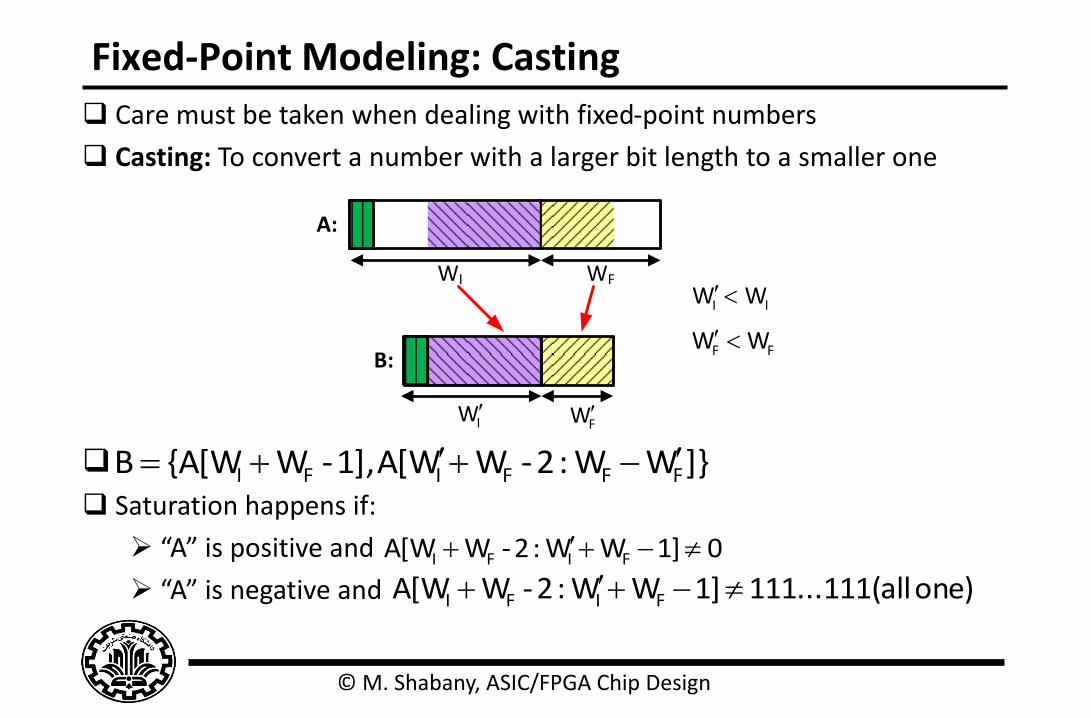
Fixed-Point Modeling: Casting
Care must be taken when dealing with fixed-point numbers
Casting: To convert a number with a larger bit length to a smaller one
Saturation happens if:
“A” is positive and
“A” is negative and
]}WW:2-WWA[1],-W{A[WB FFFIFI
WI WF
IWFW
II WW
FF WW B:
A:
one) (all 111...1111]WW:2-WA[W FIFI
01]WW:2-WA[W FIFI
© M. Shabany, ASIC/FPGA Chip Design
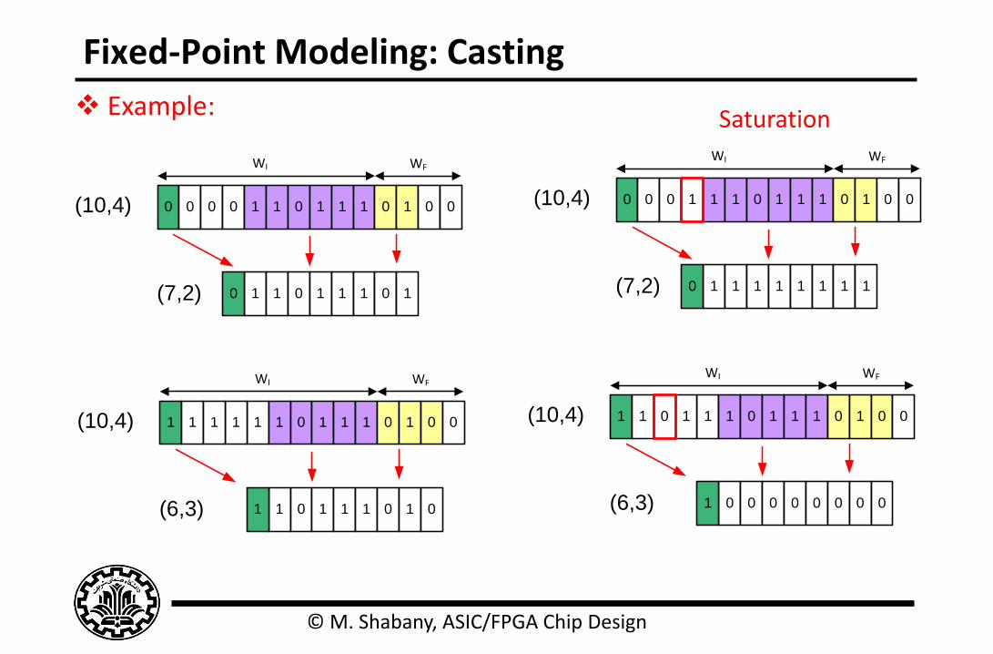
Fixed-Point Modeling: Casting
Example:
0 0 0 0 1 1 0 1 1 1 0 1 0 0
WI WF
1 1 0 1 1 1 0 10
(10,4)
(7,2)
0 0 0 1 1 0 1 1 1 0 1 0 0
WI WF
1 1 1 1 1 1 1 10
(10,4)
(7,2)
1
1 1 1 1 0 1 1 1 0 1 0 0
WI WF
0 0 0 0 0 0 0 01
(10,4)
(6,3)
101 1 1 1 0 1 1 1 0 1 0 0
WI WF
1 0 1 1 1 0 1 01
(10,4)
(6,3)
11
Saturation
© M. Shabany, ASIC/FPGA Chip Design
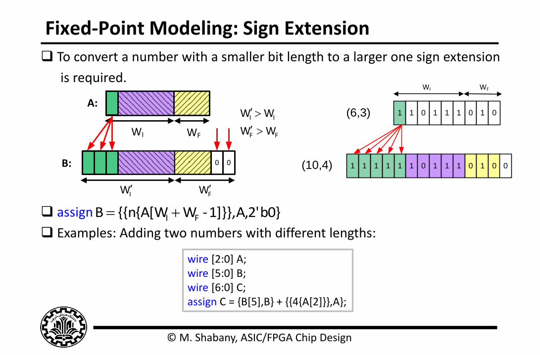
Fixed-Point Modeling: Sign Extension
To convert a number with a smaller bit length to a larger one sign extension
is required.
assign
Examples: Adding two numbers with different lengths:
b0}A,2'1]}},-W{{n{A[WB FI
wire [2:0] A; wire [5:0] B; wire [6:0] C; assign C = {B[5],B} + {{4{A[2]}},A};
1 0 1 1 1 0 1 0
WI WF
(10,4)
1 0 1 1 1 0 1 01(6,3)
11111 0
WI WF
IWFW
B:
A:II WW
FF WW
00
© M. Shabany, ASIC/FPGA Chip Design
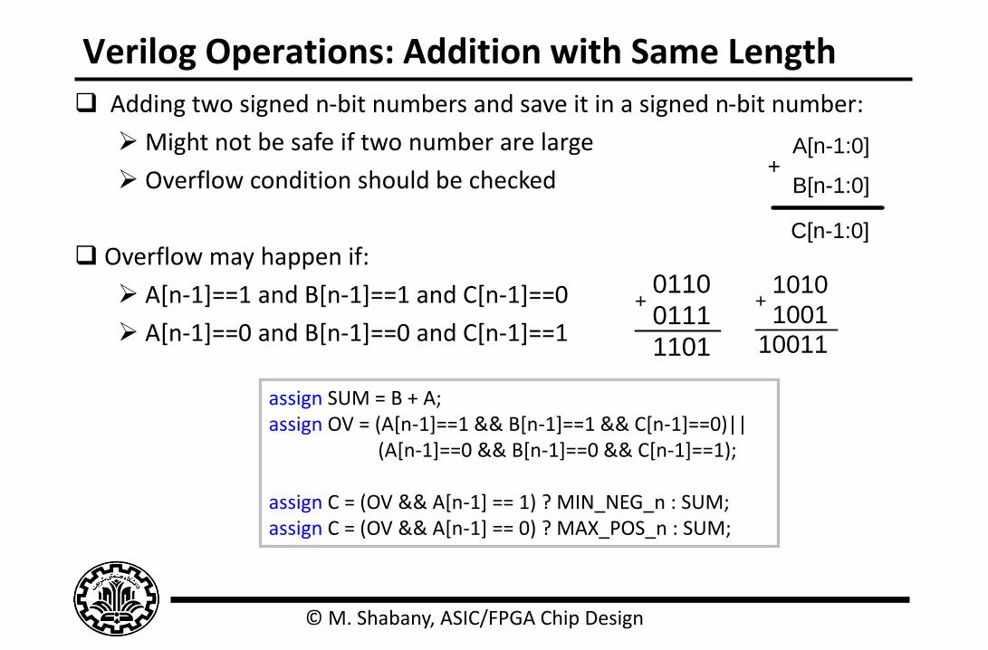
Verilog Operations: Addition with Same Length
Adding two signed n-bit numbers and save it in a signed n-bit number:
Might not be safe if two number are large
Overflow condition should be checked
Overflow may happen if:
A[n-1]==1 and B[n-1]==1 and C[n-1]==0
A[n-1]==0 and B[n-1]==0 and C[n-1]==1
assign SUM = B + A; assign OV = (A[n-1]==1 && B[n-1]==1 && C[n-1]==0)|| (A[n-1]==0 && B[n-1]==0 && C[n-1]==1); assign C = (OV && A[n-1] == 1) ? MIN_NEG_n : SUM; assign C = (OV && A[n-1] == 0) ? MAX_POS_n : SUM;
A[n-1:0]
B[n-1:0]
C[n-1:0]
+
0110
0111
1101
+1010
1001+
10011
© M. Shabany, ASIC/FPGA Chip Design
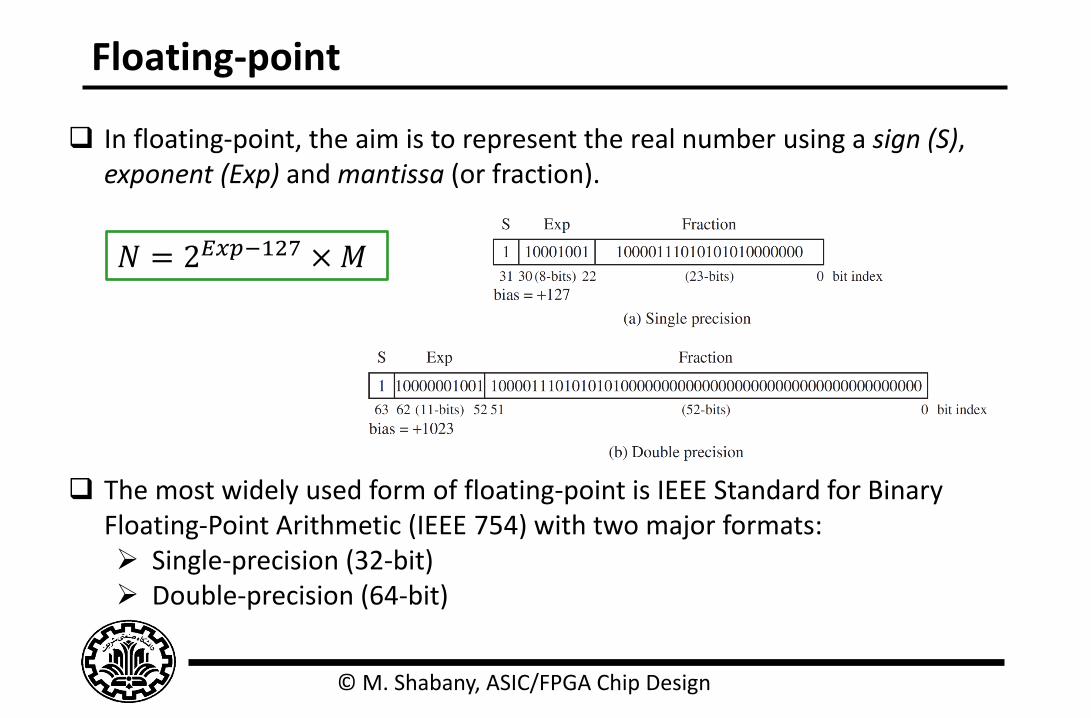
Floating-point
In floating-point, the aim is to represent the real number using a sign (S), exponent (Exp) and mantissa (or fraction).
The most widely used form of floating-point is IEEE Standard for Binary Floating-Point Arithmetic (IEEE 754) with two major formats: Single-precision (32-bit) Double-precision (64-bit)
𝑁 = 2𝐸𝑥𝑝−127 ×𝑀

© M. Shabany, ASIC/FPGA Chip Design
Floating-point: Example
Converting a real number, −1082.5674 IEEE 754 floating-point representation: It can be determined that S = 1 as the number is negative. The number (1082) is converted to binary by successive division, 10000111010. The fractional part (0.65625) is computed in the same way as above, giving 10101. The parts are combined to give the value 10000111010.10101. The radix point is moved left, to leave a single 1 on the left, 1.000011101010101 × 210. Filling with 0s to get the 23-bit mantissa gives the value 10000111010101010000000. The exponent is 10 and with the 32-bit IEEE 754 format bias of 127, giving 137 which is
given as 10001001 in binary.
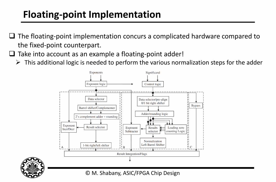
© M. Shabany, ASIC/FPGA Chip Design
Floating-point Implementation
The floating-point implementation concurs a complicated hardware compared to the fixed-point counterpart.
Take into account as an example a floating-point adder! This additional logic is needed to perform the various normalization steps for the adder
implementation.

© M. Shabany, ASIC/FPGA Chip Design
Fixed-point vs. Floating-point
The area comparison for floating-point is additionally complicated as the relationship between multiplier and adder area is now changed.
In fixed-point, multipliers are generally viewed to be N times bigger than adders where N is the word length.
However, in floating-point, the area of floating-point adders is comparable to that of floating-point multipliers which corrupts the assumption at the algorithmic stages to reduce number of multiplications in favor of additions.
Table below gives some figures on area and speed figures for floating-point addition and multiplication implemented in a Xilinx Virtex 4 FPGA technology.
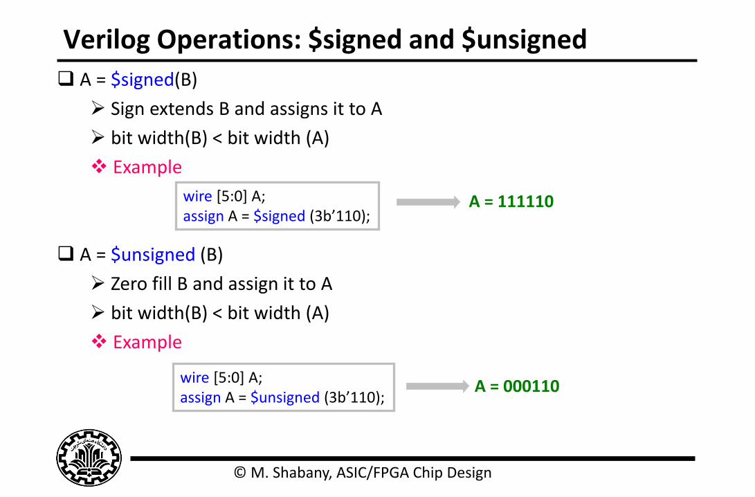
© M. Shabany, ASIC/FPGA Chip Design
Verilog Operations: $signed and $unsigned
A = $signed(B)
Sign extends B and assigns it to A
bit width(B) < bit width (A)
Example
A = $unsigned (B)
Zero fill B and assign it to A
bit width(B) < bit width (A)
Example
wire [5:0] A; assign A = $signed (3b’110);
wire [5:0] A; assign A = $unsigned (3b’110);
A = 111110
A = 000110
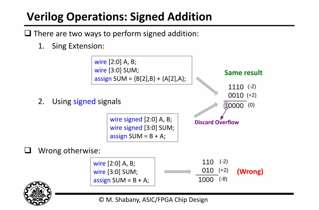
© M. Shabany, ASIC/FPGA Chip Design
Verilog Operations: Signed Addition
There are two ways to perform signed addition:
1. Sing Extension:
2. Using signed signals
Wrong otherwise:
wire [2:0] A, B; wire [3:0] SUM; assign SUM = {B[2],B} + {A[2],A};
wire signed [2:0] A, B; wire signed [3:0] SUM; assign SUM = B + A;
Same result
wire [2:0] A, B; wire [3:0] SUM; assign SUM = B + A;
110
010
1000
(-2)
(+2)
(-8)
(Wrong)
1110
0010
10000
Discard Overflow
(-2)
(+2)
(0)
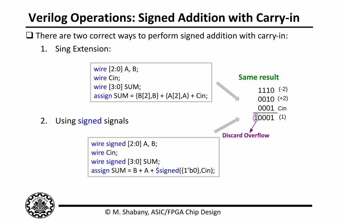
© M. Shabany, ASIC/FPGA Chip Design
Verilog Operations: Signed Addition with Carry-in
There are two correct ways to perform signed addition with carry-in:
1. Sing Extension:
2. Using signed signals
wire [2:0] A, B; wire Cin; wire [3:0] SUM; assign SUM = {B[2],B} + {A[2],A} + Cin;
wire signed [2:0] A, B; wire Cin; wire signed [3:0] SUM; assign SUM = B + A + $signed({1’b0},Cin);
Same result
1110
0010
0001
10001
Discard Overflow
(-2)
(+2)
(1)
Cin
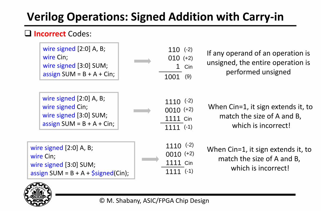
© M. Shabany, ASIC/FPGA Chip Design
Verilog Operations: Signed Addition with Carry-in
Incorrect Codes:
wire signed [2:0] A, B; wire Cin; wire signed [3:0] SUM; assign SUM = B + A + Cin;
If any operand of an operation is unsigned, the entire operation is
performed unsigned
wire signed [2:0] A, B; wire Cin; wire signed [3:0] SUM; assign SUM = B + A + $signed(Cin);
110
010
1
1001
(-2)
(+2)
(9)
Cin
1110
0010
1111
1111
(-2)
(+2)
(-1)
Cin
wire signed [2:0] A, B; wire signed Cin; wire signed [3:0] SUM; assign SUM = B + A + Cin;
1110
0010
1111
1111
(-2)
(+2)
(-1)
Cin
When Cin=1, it sign extends it, to match the size of A and B,
which is incorrect!
When Cin=1, it sign extends it, to match the size of A and B,
which is incorrect!

© M. Shabany, ASIC/FPGA Chip Design
Verilog Operations: Signed Multiplication
Use signed construct as we used for signed addition:
1. Use Verilog constructs:
2. Write it manually as a module
Complicated!
wire signed [16:0] A, B; wire signed [31:0] MULT; assign MULT = A*B;
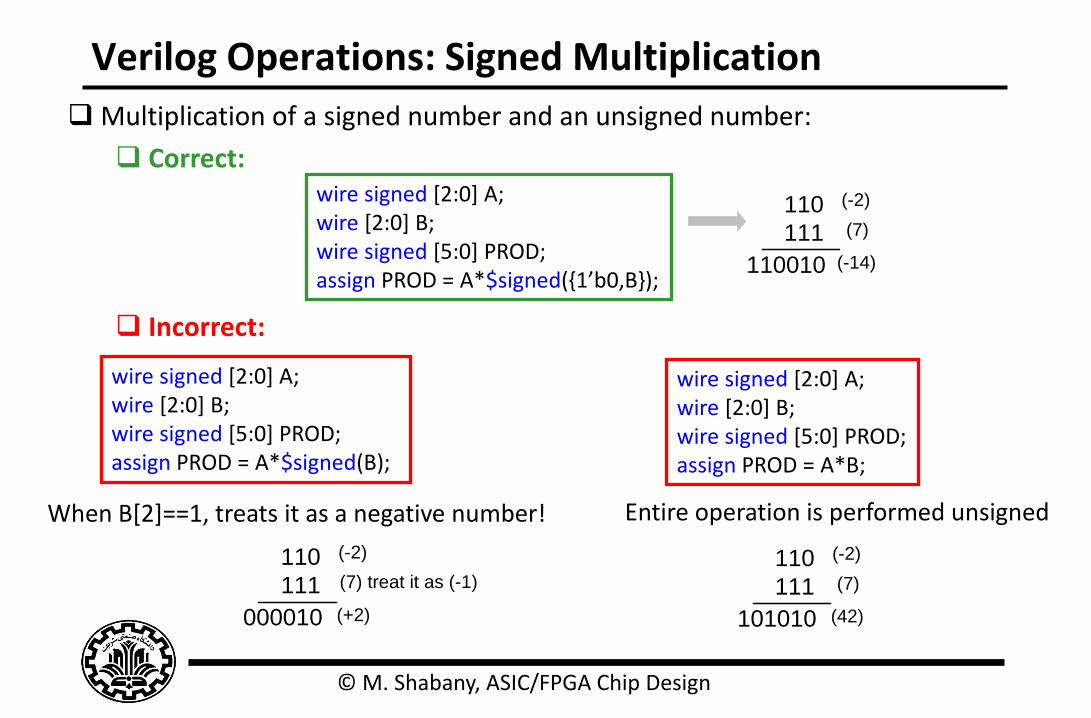
© M. Shabany, ASIC/FPGA Chip Design
Verilog Operations: Signed Multiplication
Multiplication of a signed number and an unsigned number:
Correct:
Incorrect:
wire signed [2:0] A; wire [2:0] B; wire signed [5:0] PROD; assign PROD = A*$signed({1’b0,B});
wire signed [2:0] A; wire [2:0] B; wire signed [5:0] PROD; assign PROD = A*$signed(B);
wire signed [2:0] A; wire [2:0] B; wire signed [5:0] PROD; assign PROD = A*B;
When B[2]==1, treats it as a negative number! Entire operation is performed unsigned
110
111
101010
(-2)
(7)
(42)
110
111
000010
(-2)
(7) treat it as (-1)
(+2)
110
111
110010
(-2)
(7)
(-14)
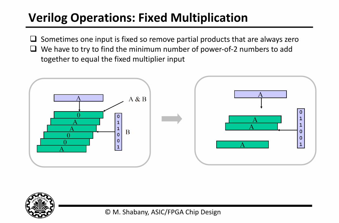
© M. Shabany, ASIC/FPGA Chip Design
Verilog Operations: Fixed Multiplication
Sometimes one input is fixed so remove partial products that are always zero We have to try to find the minimum number of power‐of‐2 numbers to add
together to equal the fixed multiplier input
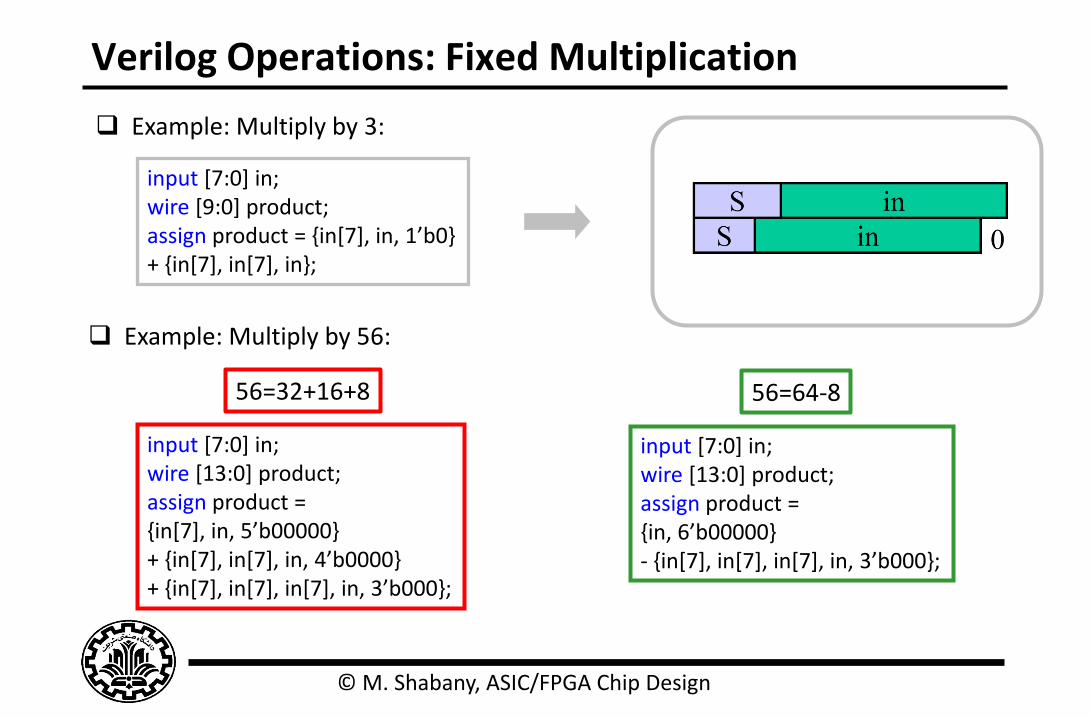
© M. Shabany, ASIC/FPGA Chip Design
Verilog Operations: Fixed Multiplication
Example: Multiply by 3:
input [7:0] in; wire [9:0] product; assign product = {in[7], in, 1’b0} + {in[7], in[7], in};
Example: Multiply by 56:
input [7:0] in; wire [13:0] product; assign product = {in[7], in, 5’b00000} + {in[7], in[7], in, 4’b0000} + {in[7], in[7], in[7], in, 3’b000};
56=32+16+8
input [7:0] in; wire [13:0] product; assign product = {in, 6’b00000} - {in[7], in[7], in[7], in, 3’b000};
56=64-8

© M. Shabany, ASIC/FPGA Chip Design
Verilog Operations: Constant Multiplication
Multiplication with a set of constant numbers may be implemented more
efficiently:
}-1,1,3,5,7{-7,-5,-3,b baP
0111
0101
0011
0001
1111
1101
1011
1001
3 24M
SB
1L
SB
b
b[4]
b[3]b[2]
b[4]b[3]b[4]b[3]
<<1 <<2
SUM SUM SUM
<<3
01 01 01
010
01
a
P=axb
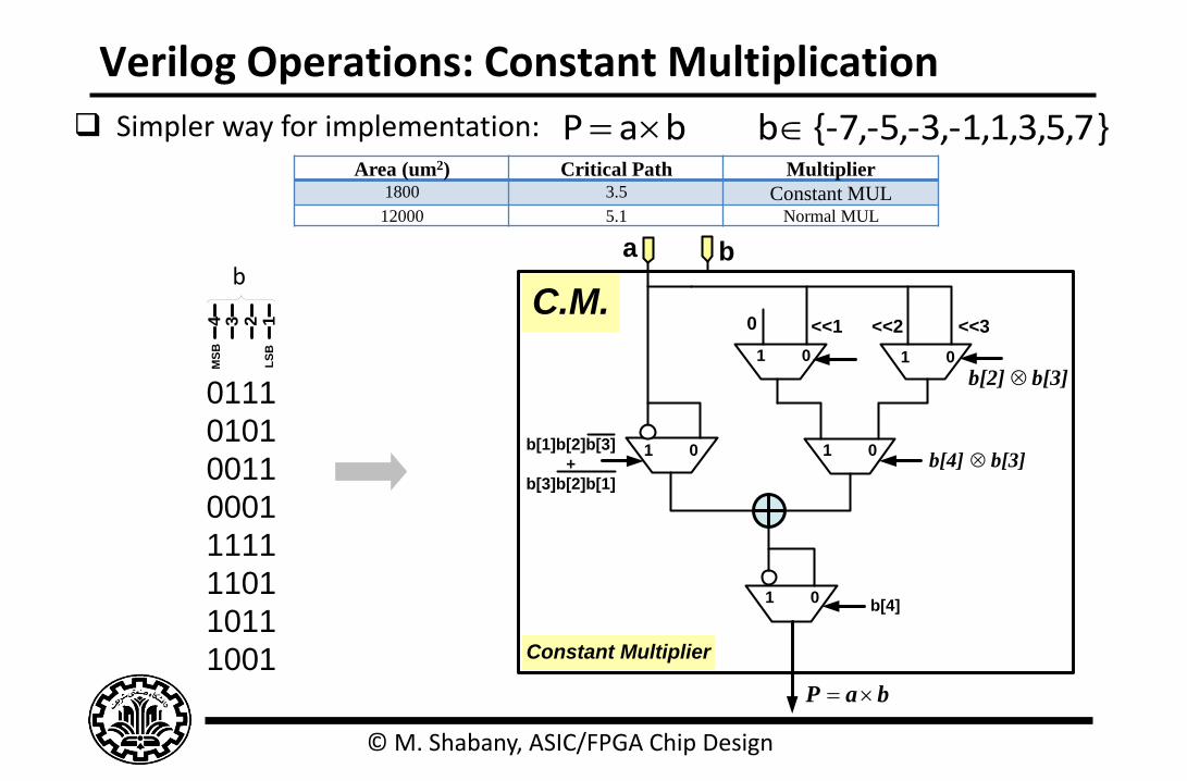
© M. Shabany, ASIC/FPGA Chip Design
Verilog Operations: Constant Multiplication
Simpler way for implementation:
}-1,1,3,5,7{-7,-5,-3,b baP
0111
0101
0011
0001
1111
1101
1011
1001
3 24M
SB
1L
SB
ba
1 0
1 0 1 0
1 0
1 0
<<10 <<2 <<3
baP
b[4]
b[3]b[4]
b[3]b[2]
b
C.M.
Constant Multiplier
b[1]b[2]b[3]
+
b[3]b[2]b[1]
Multiplier Critical Path Area (um2)
Constant MUL 3.5 1800
Normal MUL 5.1 12000
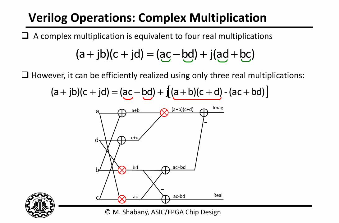
© M. Shabany, ASIC/FPGA Chip Design
Verilog Operations: Complex Multiplication
A complex multiplication is equivalent to four real multiplications
However, it can be efficiently realized using only three real multiplications:
bc)j(adbd)(acjd)jb)(c(a
bd)(ac-d)b)(c(ajbd)(acjd)jb)(c(a
a
b
a+b
c
d
bd
ac
c+d
-
(a+b)(c+d)
ac-bd
ac+bd
-
Imag
Real
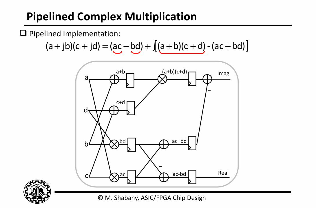
© M. Shabany, ASIC/FPGA Chip Design
Pipelined Complex Multiplication
Pipelined Implementation:
bd)(ac-d)b)(c(ajbd)(acjd)jb)(c(a
a
b
a+b
c
d
bd
ac
c+d
-
(a+b)(c+d)
ac-bd
ac+bd
-
Imag
Real
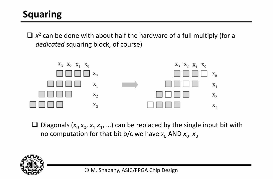
© M. Shabany, ASIC/FPGA Chip Design
Squaring
x2 can be done with about half the hardware of a full multiply (for a dedicated squaring block, of course)
0x
0x
1x
1x
2x
2x
3x
3x
Diagonals (x0 x0, x1 x1, …) can be replaced by the single input bit with no computation for that bit b/c we have x0 AND x0= x0
0x1x2x3x
0x
1x
2x
3x
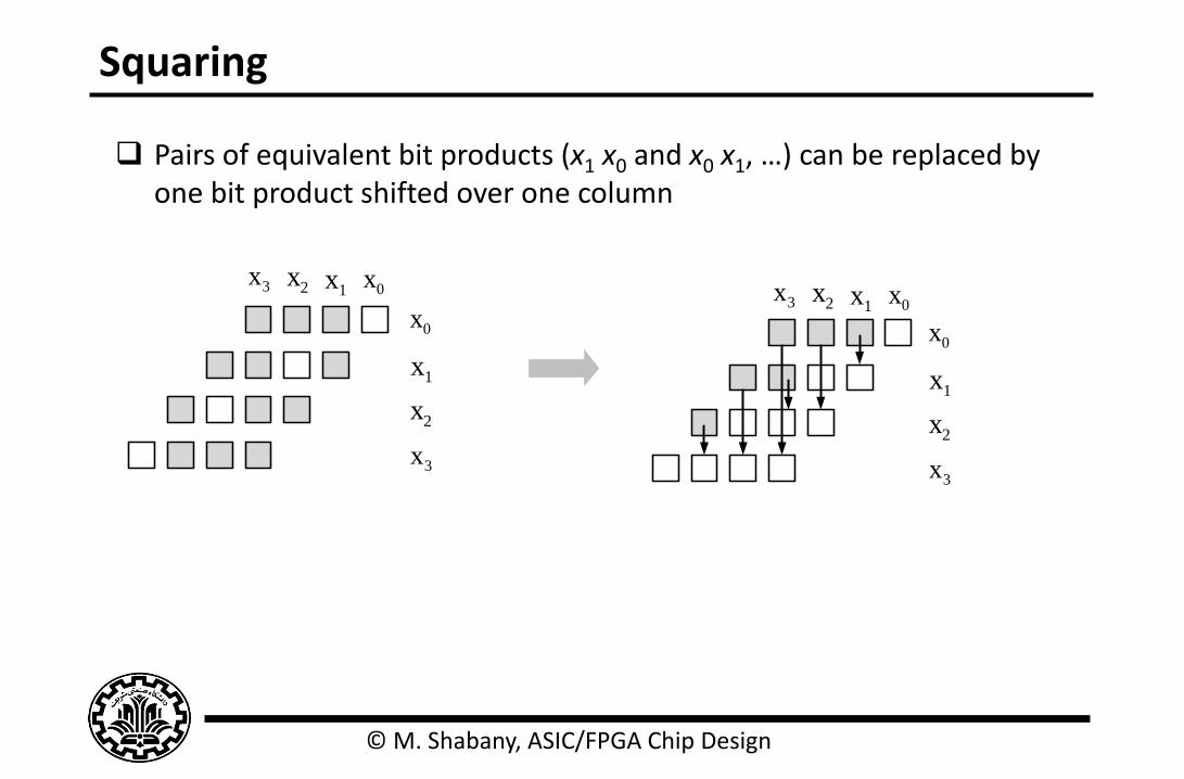
© M. Shabany, ASIC/FPGA Chip Design
Squaring
Pairs of equivalent bit products (x1 x0 and x0 x1, …) can be replaced by one bit product shifted over one column
0x1x2x3x
0x
1x
2x
3x
0x1x2x3x
0x
1x
2x
3x
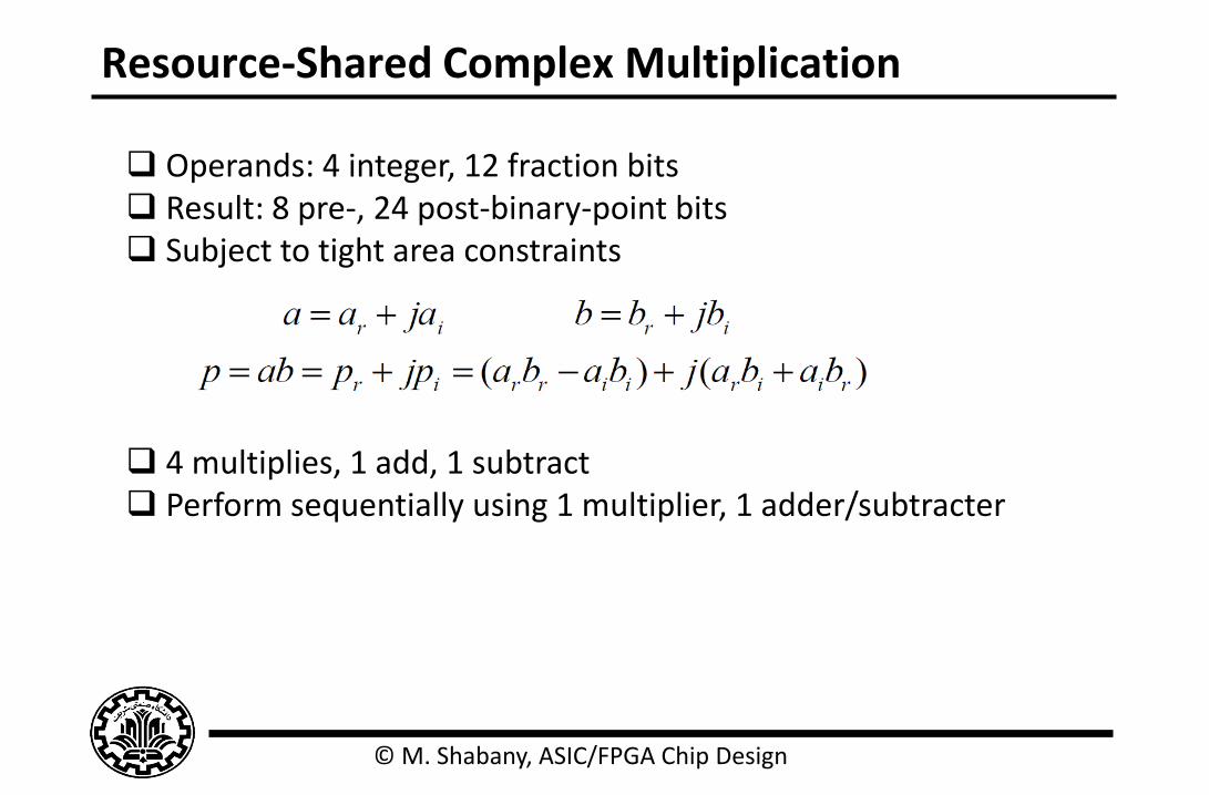
© M. Shabany, ASIC/FPGA Chip Design
Resource-Shared Complex Multiplication
Operands: 4 integer, 12 fraction bits Result: 8 pre-, 24 post-binary-point bits Subject to tight area constraints
4 multiplies, 1 add, 1 subtract Perform sequentially using 1 multiplier, 1 adder/subtracter
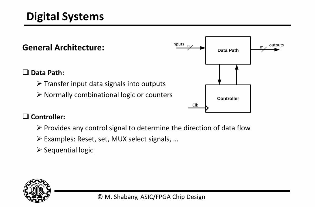
© M. Shabany, ASIC/FPGA Chip Design
Digital Systems
General Architecture:
Data Path:
Transfer input data signals into outputs
Normally combinational logic or counters
Controller:
Provides any control signal to determine the direction of data flow
Examples: Reset, set, MUX select signals, …
Sequential logic
Data Path
Controller
n minputs outputs
Clk
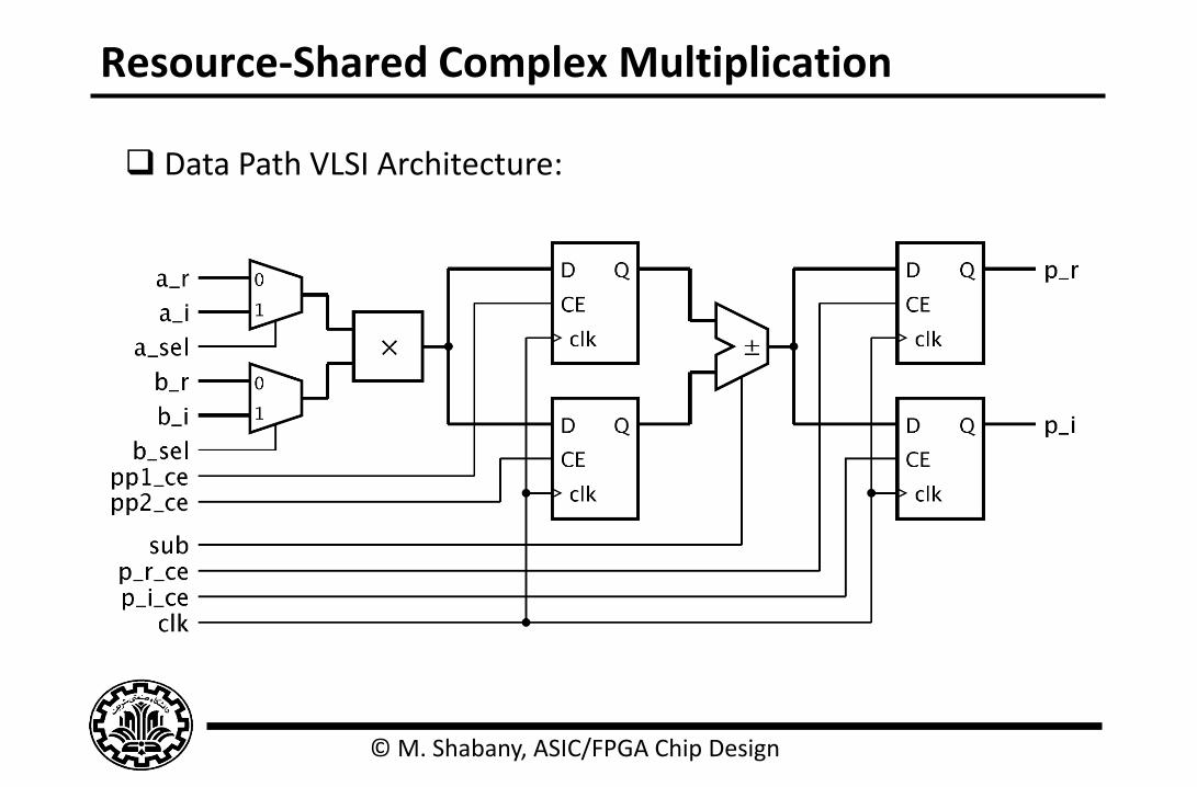
© M. Shabany, ASIC/FPGA Chip Design
Resource-Shared Complex Multiplication
Data Path VLSI Architecture:
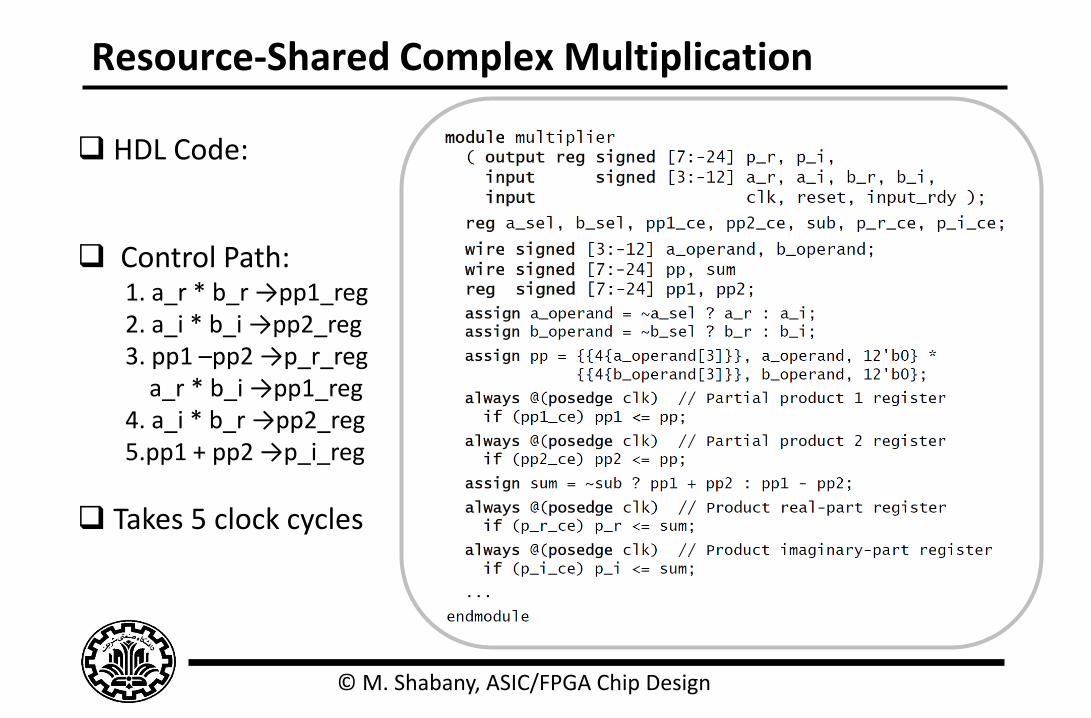
© M. Shabany, ASIC/FPGA Chip Design
Resource-Shared Complex Multiplication
HDL Code:
Control Path: 1. a_r * b_r →pp1_reg 2. a_i * b_i →pp2_reg 3. pp1 –pp2 →p_r_reg a_r * b_i →pp1_reg 4. a_i * b_r →pp2_reg 5.pp1 + pp2 →p_i_reg
Takes 5 clock cycles

© M. Shabany, ASIC/FPGA Chip Design
Resource-Shared Complex Multiplication
Control Logic (Timing Schedule):
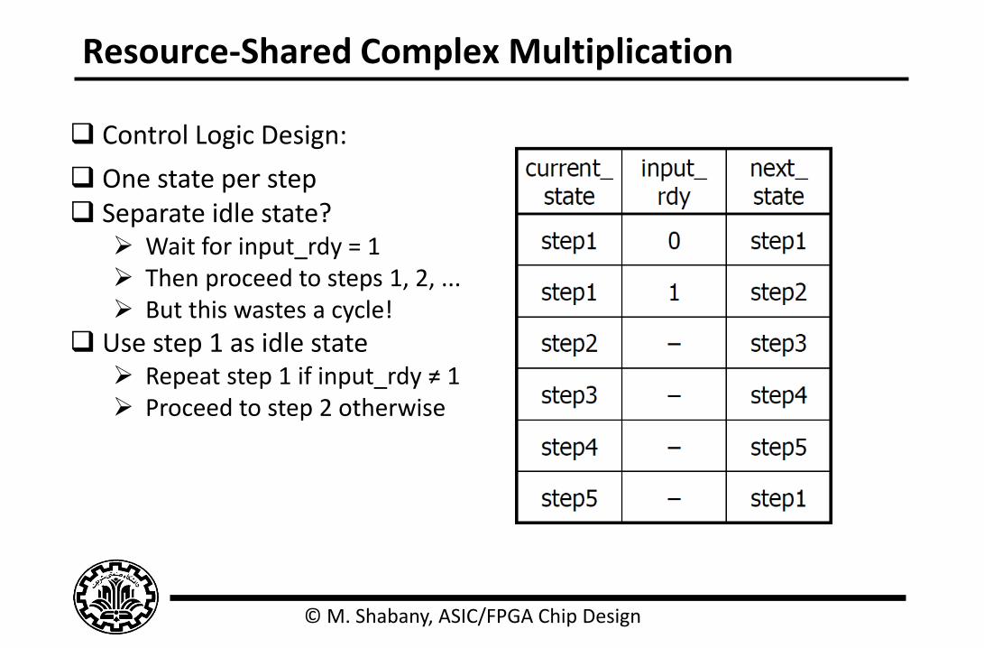
© M. Shabany, ASIC/FPGA Chip Design
Resource-Shared Complex Multiplication
Control Logic Design:
One state per step Separate idle state?
Wait for input_rdy = 1 Then proceed to steps 1, 2, ... But this wastes a cycle!
Use step 1 as idle state Repeat step 1 if input_rdy ≠ 1 Proceed to step 2 otherwise
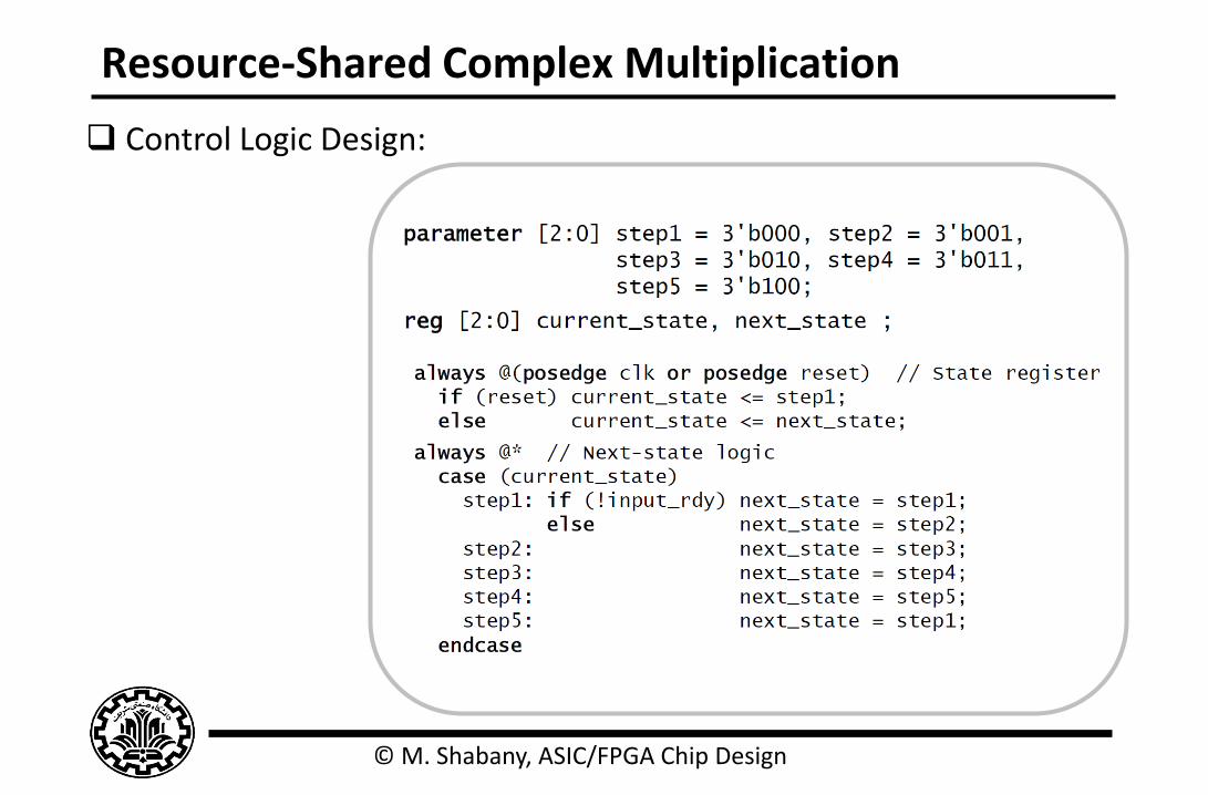
© M. Shabany, ASIC/FPGA Chip Design
Resource-Shared Complex Multiplication
Control Logic Design:
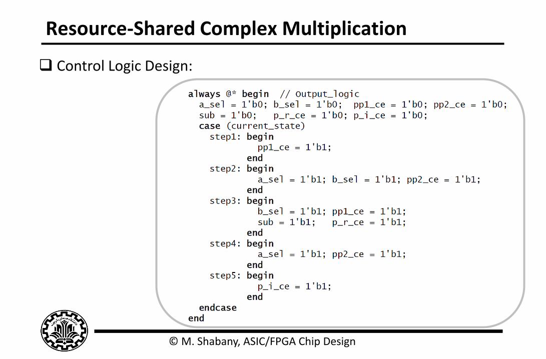
© M. Shabany, ASIC/FPGA Chip Design
Resource-Shared Complex Multiplication
Control Logic Design:
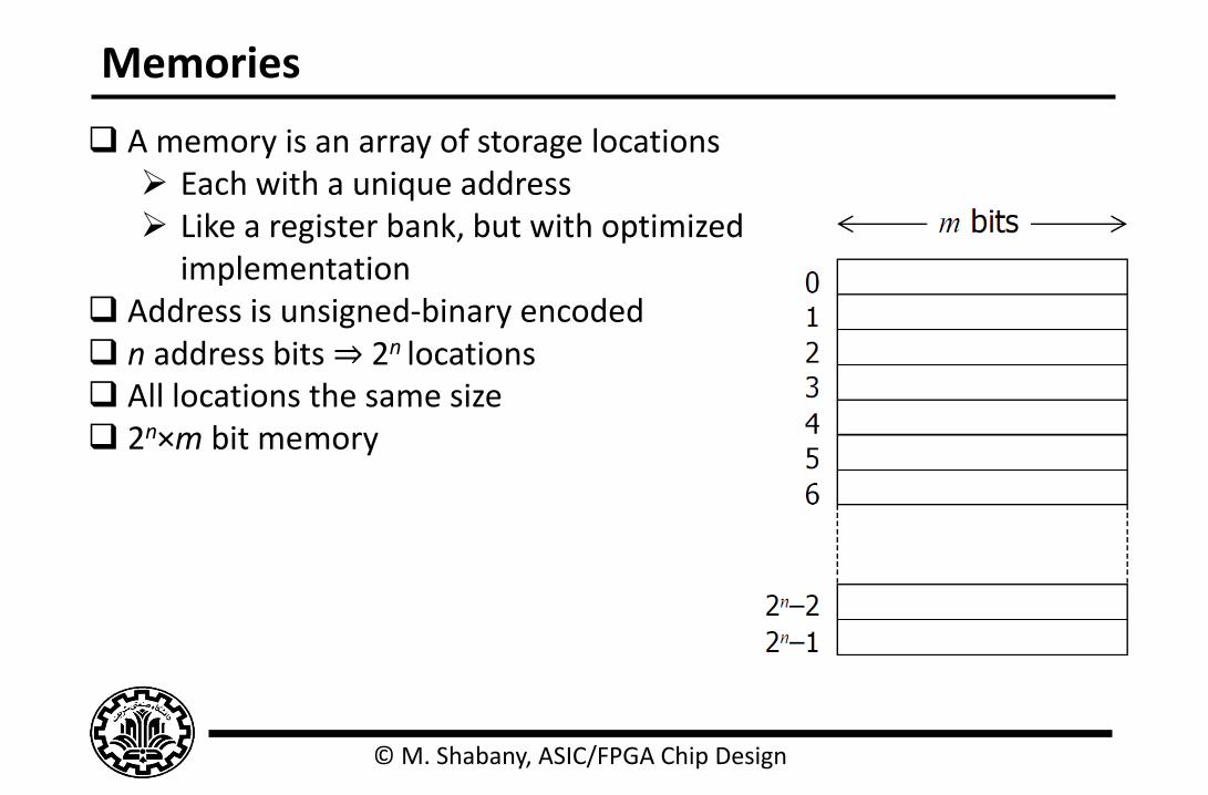
© M. Shabany, ASIC/FPGA Chip Design
Memories
A memory is an array of storage locations Each with a unique address Like a register bank, but with optimized
implementation Address is unsigned-binary encoded n address bits ⇒ 2n locations All locations the same size 2n×m bit memory

© M. Shabany, ASIC/FPGA Chip Design
Memory Sizes
Use power-of-2 multipliers Kilo (K): 210= 1,024 ≈ 103
Mega (M): 220= 1,048,576 ≈ 106
Giga (G): 230= 1,073,741,824 ≈ 109
Example: 32K ×32-bit memory Capacity = 1,024K = 1Mbit Requires 15 address bits
Size is determined by application requirements
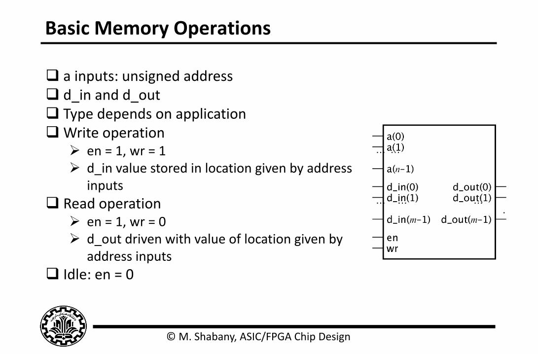
© M. Shabany, ASIC/FPGA Chip Design
Basic Memory Operations
a inputs: unsigned address d_in and d_out Type depends on application Write operation
en = 1, wr = 1 d_in value stored in location given by address
inputs
Read operation en = 1, wr = 0 d_out driven with value of location given by
address inputs
Idle: en = 0
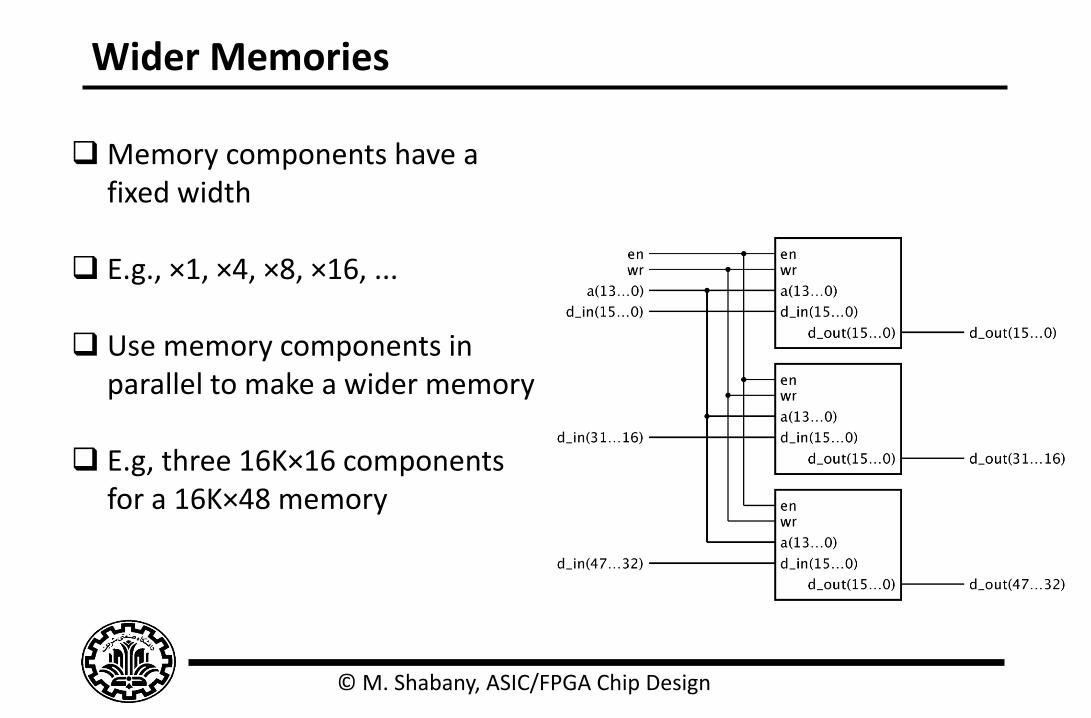
© M. Shabany, ASIC/FPGA Chip Design
Wider Memories
Memory components have a fixed width
E.g., ×1, ×4, ×8, ×16, ...
Use memory components in parallel to make a wider memory
E.g, three 16K×16 components for a 16K×48 memory
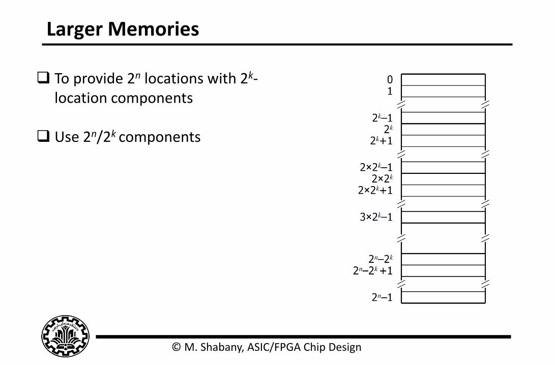
© M. Shabany, ASIC/FPGA Chip Design
Larger Memories
To provide 2n locations with 2k-location components
Use 2n/2k components
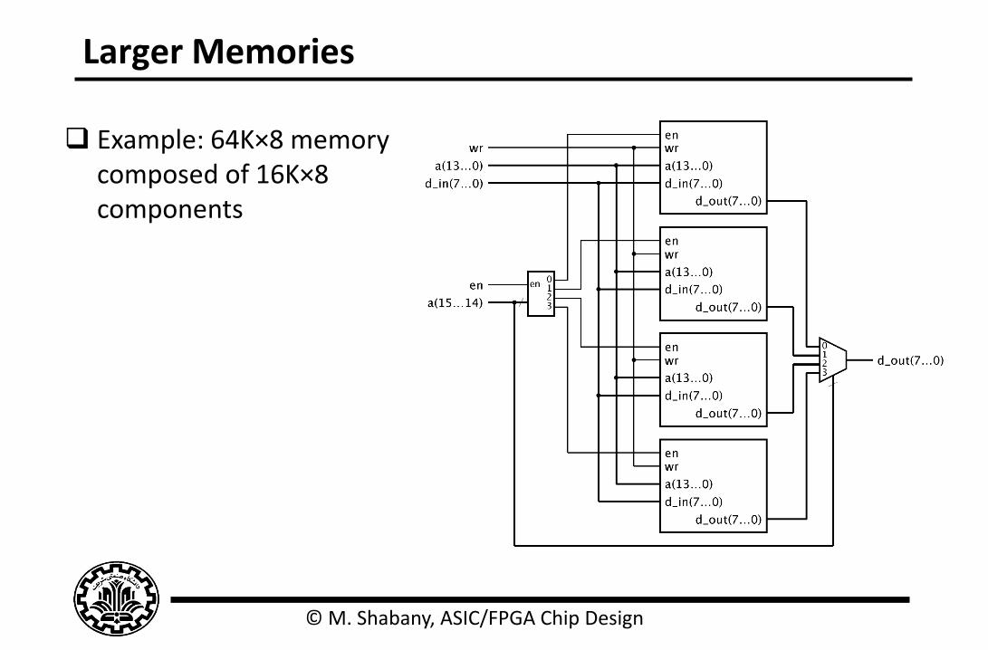
© M. Shabany, ASIC/FPGA Chip Design
Larger Memories
Example: 64K×8 memory composed of 16K×8 components
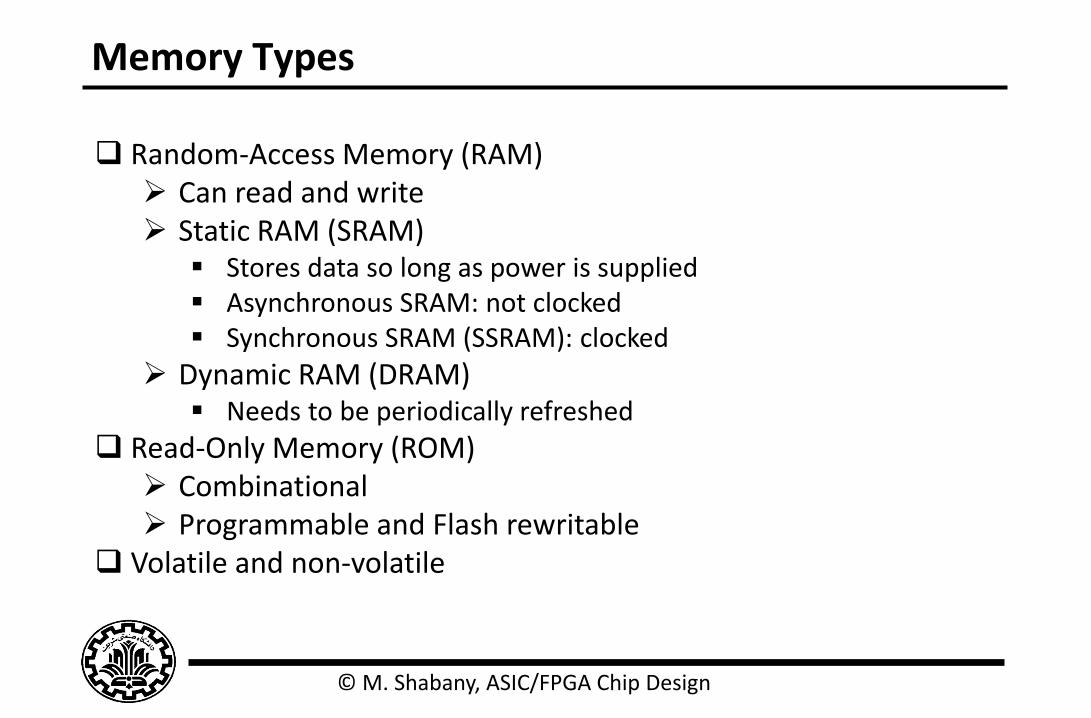
© M. Shabany, ASIC/FPGA Chip Design
Memory Types
Random-Access Memory (RAM) Can read and write Static RAM (SRAM)
Stores data so long as power is supplied Asynchronous SRAM: not clocked Synchronous SRAM (SSRAM): clocked
Dynamic RAM (DRAM) Needs to be periodically refreshed
Read-Only Memory (ROM) Combinational Programmable and Flash rewritable
Volatile and non-volatile

© M. Shabany, ASIC/FPGA Chip Design
Verilog Memories: Single-Port vs. Dual-Port RAM
Single-port RAM (SPRAM):
Can only be accessed at one address at one time
Read or Write (not both) one memory cell at a time in each clock cycle
Dual-port RAM (DPRAM):
Can be accessed at two addresses at one time
Read & Write different memory cells at different addresses simultaneously
DPRAM
In0 Out0
Add0
In1 Out1
Add1
SPRAM
In Out
Add
Read
Read
Write
Write
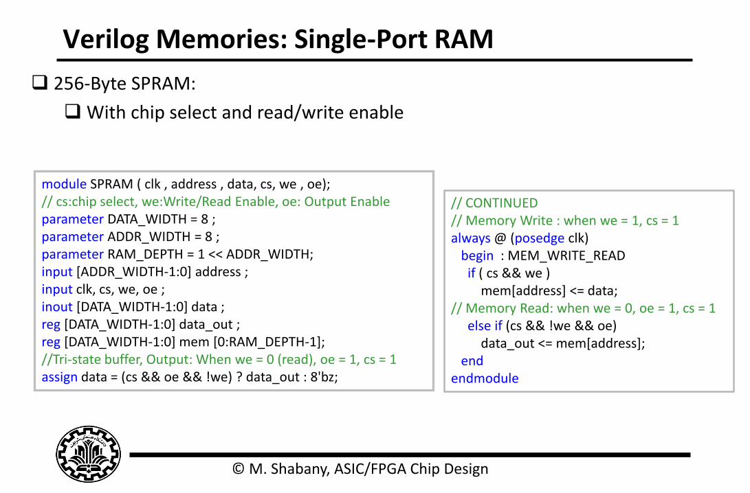
© M. Shabany, ASIC/FPGA Chip Design
Verilog Memories: Single-Port RAM
256-Byte SPRAM:
With chip select and read/write enable
module SPRAM ( clk , address , data, cs, we , oe); // cs:chip select, we:Write/Read Enable, oe: Output Enable parameter DATA_WIDTH = 8 ; parameter ADDR_WIDTH = 8 ; parameter RAM_DEPTH = 1 << ADDR_WIDTH; input [ADDR_WIDTH-1:0] address ; input clk, cs, we, oe ; inout [DATA_WIDTH-1:0] data ; reg [DATA_WIDTH-1:0] data_out ; reg [DATA_WIDTH-1:0] mem [0:RAM_DEPTH-1]; //Tri-state buffer, Output: When we = 0 (read), oe = 1, cs = 1 assign data = (cs && oe && !we) ? data_out : 8'bz;
// CONTINUED // Memory Write : when we = 1, cs = 1 always @ (posedge clk) begin : MEM_WRITE_READ if ( cs && we ) mem[address] <= data; // Memory Read: when we = 0, oe = 1, cs = 1 else if (cs && !we && oe) data_out <= mem[address]; end endmodule
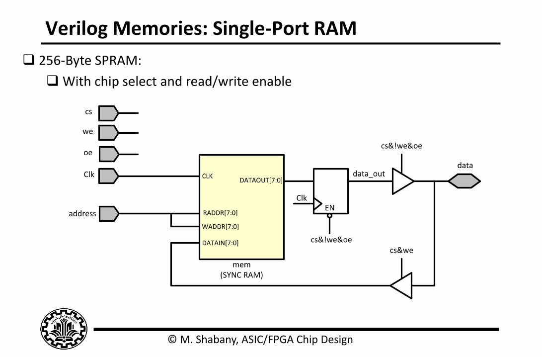
© M. Shabany, ASIC/FPGA Chip Design
Verilog Memories: Single-Port RAM
256-Byte SPRAM:
With chip select and read/write enable
Clk
data_out
cs&!we&oe
EN
mem(SYNC RAM)
DATAOUT[7:0]
DATAIN[7:0]
WADDR[7:0]
RADDR[7:0]
data
cs&!we&oe
cs&we
address
Clk CLK
oe
we
cs
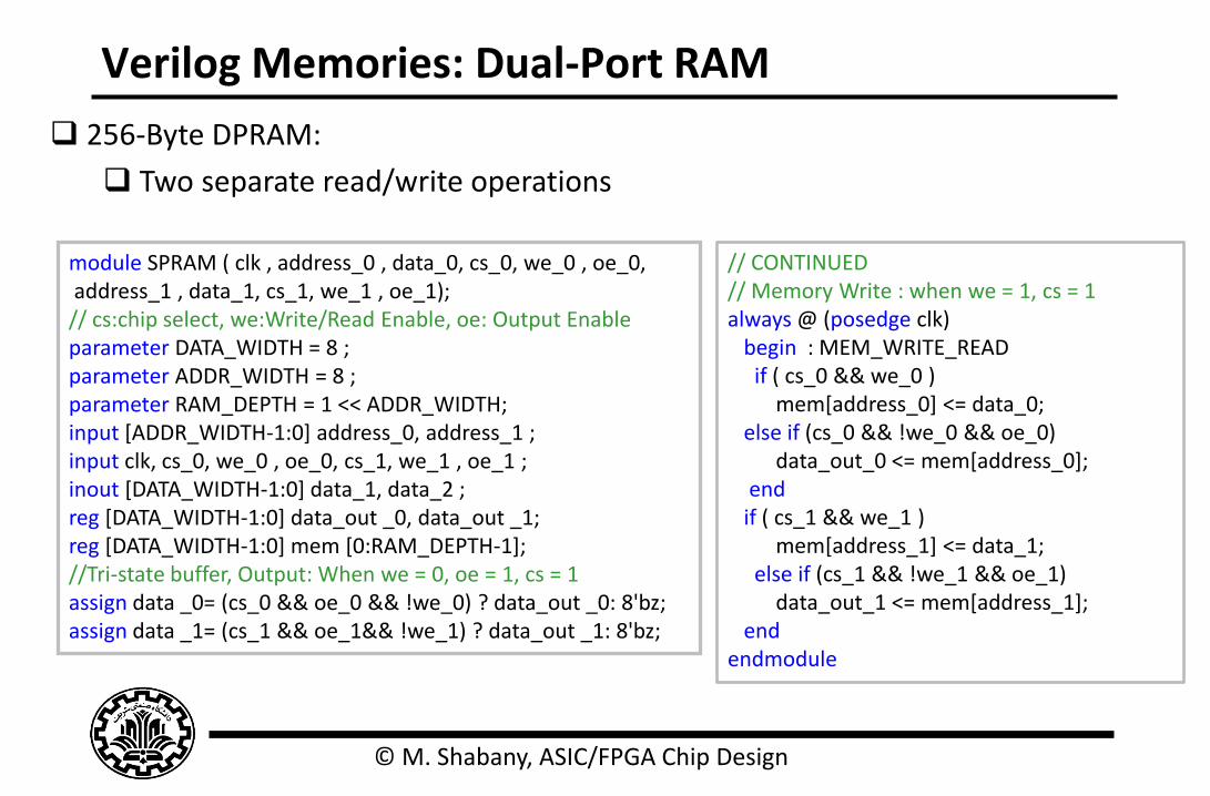
© M. Shabany, ASIC/FPGA Chip Design
Verilog Memories: Dual-Port RAM
256-Byte DPRAM:
Two separate read/write operations
module SPRAM ( clk , address_0 , data_0, cs_0, we_0 , oe_0, address_1 , data_1, cs_1, we_1 , oe_1); // cs:chip select, we:Write/Read Enable, oe: Output Enable parameter DATA_WIDTH = 8 ; parameter ADDR_WIDTH = 8 ; parameter RAM_DEPTH = 1 << ADDR_WIDTH; input [ADDR_WIDTH-1:0] address_0, address_1 ; input clk, cs_0, we_0 , oe_0, cs_1, we_1 , oe_1 ; inout [DATA_WIDTH-1:0] data_1, data_2 ; reg [DATA_WIDTH-1:0] data_out _0, data_out _1; reg [DATA_WIDTH-1:0] mem [0:RAM_DEPTH-1]; //Tri-state buffer, Output: When we = 0, oe = 1, cs = 1 assign data _0= (cs_0 && oe_0 && !we_0) ? data_out _0: 8'bz; assign data _1= (cs_1 && oe_1&& !we_1) ? data_out _1: 8'bz;
// CONTINUED // Memory Write : when we = 1, cs = 1 always @ (posedge clk) begin : MEM_WRITE_READ if ( cs_0 && we_0 ) mem[address_0] <= data_0; else if (cs_0 && !we_0 && oe_0) data_out_0 <= mem[address_0]; end if ( cs_1 && we_1 ) mem[address_1] <= data_1; else if (cs_1 && !we_1 && oe_1) data_out_1 <= mem[address_1]; end endmodule
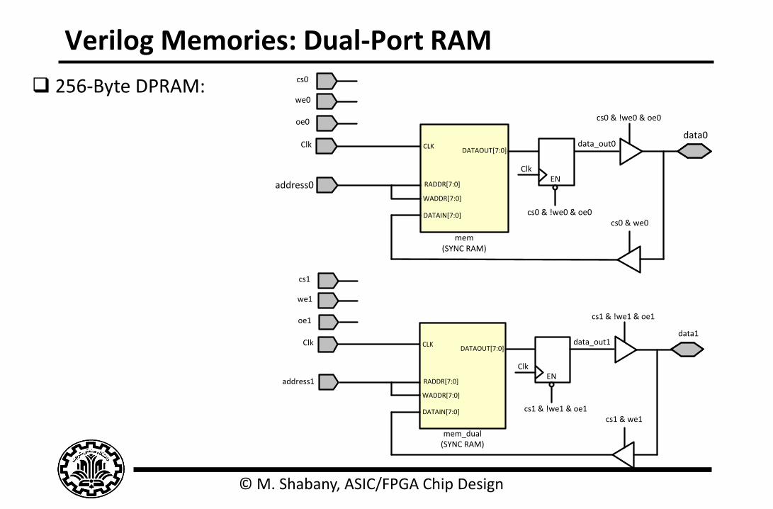
© M. Shabany, ASIC/FPGA Chip Design
Verilog Memories: Dual-Port RAM
256-Byte DPRAM:
Clk
data_out0
EN
mem(SYNC RAM)
DATAOUT[7:0]
DATAIN[7:0]
WADDR[7:0]
RADDR[7:0]
data0
cs0 & we0
address0
Clk CLK
oe0
we0
cs0
cs0 & !we0 & oe0
cs0 & !we0 & oe0
Clk
data_out1
EN
mem_dual(SYNC RAM)
DATAOUT[7:0]
DATAIN[7:0]
WADDR[7:0]
RADDR[7:0]
data1
cs1 & we1
address1
Clk CLK
oe1
we1
cs1
cs1 & !we1 & oe1
cs1 & !we1 & oe1
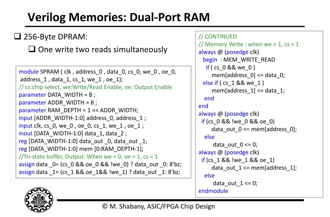
© M. Shabany, ASIC/FPGA Chip Design
Verilog Memories: Dual-Port RAM
256-Byte DPRAM:
One write two reads simultaneously
module SPRAM ( clk , address_0 , data_0, cs_0, we_0 , oe_0, address_1 , data_1, cs_1, we_1 , oe_1); // cs:chip select, we:Write/Read Enable, oe: Output Enable parameter DATA_WIDTH = 8 ; parameter ADDR_WIDTH = 8 ; parameter RAM_DEPTH = 1 << ADDR_WIDTH; input [ADDR_WIDTH-1:0] address_0, address_1 ; input clk, cs_0, we_0 , oe_0, cs_1, we_1 , oe_1 ; inout [DATA_WIDTH-1:0] data_1, data_2 ; reg [DATA_WIDTH-1:0] data_out _0, data_out _1; reg [DATA_WIDTH-1:0] mem [0:RAM_DEPTH-1]; //Tri-state buffer, Output: When we = 0, oe = 1, cs = 1 assign data _0= (cs_0 && oe_0 && !we_0) ? data_out _0: 8'bz; assign data _1= (cs_1 && oe_1&& !we_1) ? data_out _1: 8'bz;
// CONTINUED // Memory Write : when we = 1, cs = 1 always @ (posedge clk) begin : MEM_WRITE_READ if ( cs_0 && we_0 ) mem[address_0] <= data_0; else if ( cs_1 && we_1 ) mem[address_1] <= data_1; end end always @ (posedge clk) if (cs_0 && !we_0 && oe_0) data_out_0 <= mem[address_0]; else data_out_0 <= 0; always @ (posedge clk) if (cs_1 && !we_1 && oe_1) data_out_1 <= mem[address_1]; else data_out_1 <= 0; endmodule
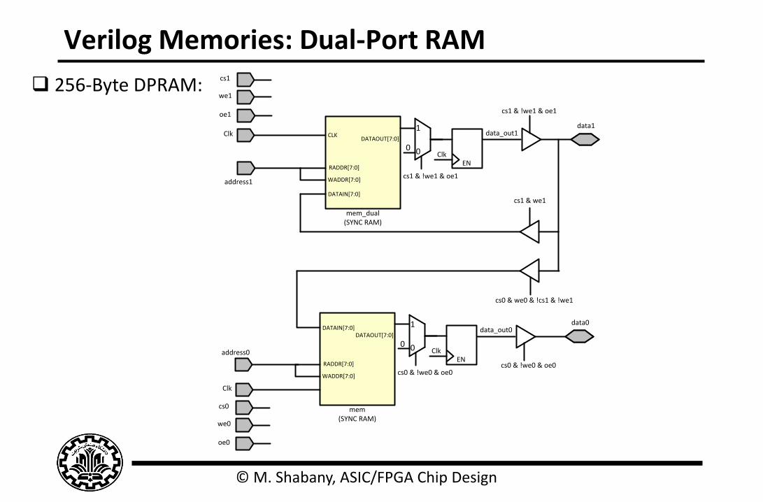
© M. Shabany, ASIC/FPGA Chip Design
Verilog Memories: Dual-Port RAM
256-Byte DPRAM:
Clk
data_out1
EN
mem_dual(SYNC RAM)
DATAOUT[7:0]
DATAIN[7:0]
WADDR[7:0]
RADDR[7:0]
data1
cs1 & we1
address1
Clk CLK
oe1
we1
cs1
cs1 & !we1 & oe1
0
1
cs1 & !we1 & oe1
0
cs0 & we0 & !cs1 & !we1
ClkEN
mem(SYNC RAM)
DATAOUT[7:0]DATAIN[7:0]
WADDR[7:0]
RADDR[7:0]
0
1
cs0 & !we0 & oe0
0address0
Clk
oe0
we0
cs0
data_out0data0
cs0 & !we0 & oe0
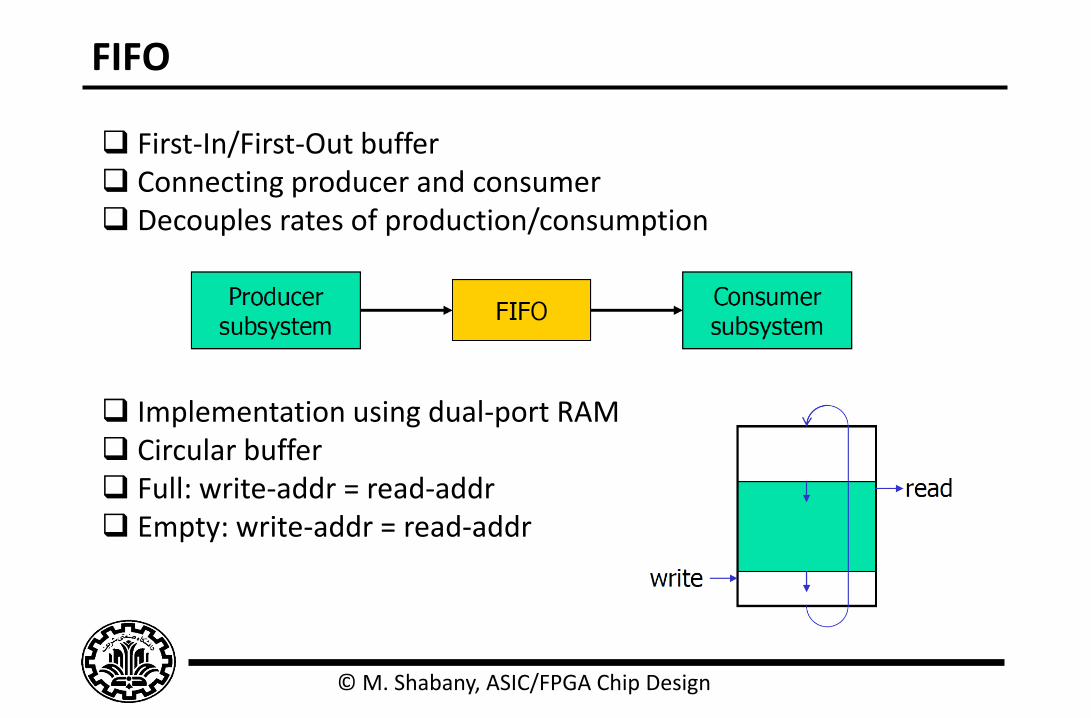
© M. Shabany, ASIC/FPGA Chip Design
FIFO
First-In/First-Out buffer Connecting producer and consumer Decouples rates of production/consumption
Implementation using dual-port RAM Circular buffer Full: write-addr = read-addr Empty: write-addr = read-addr
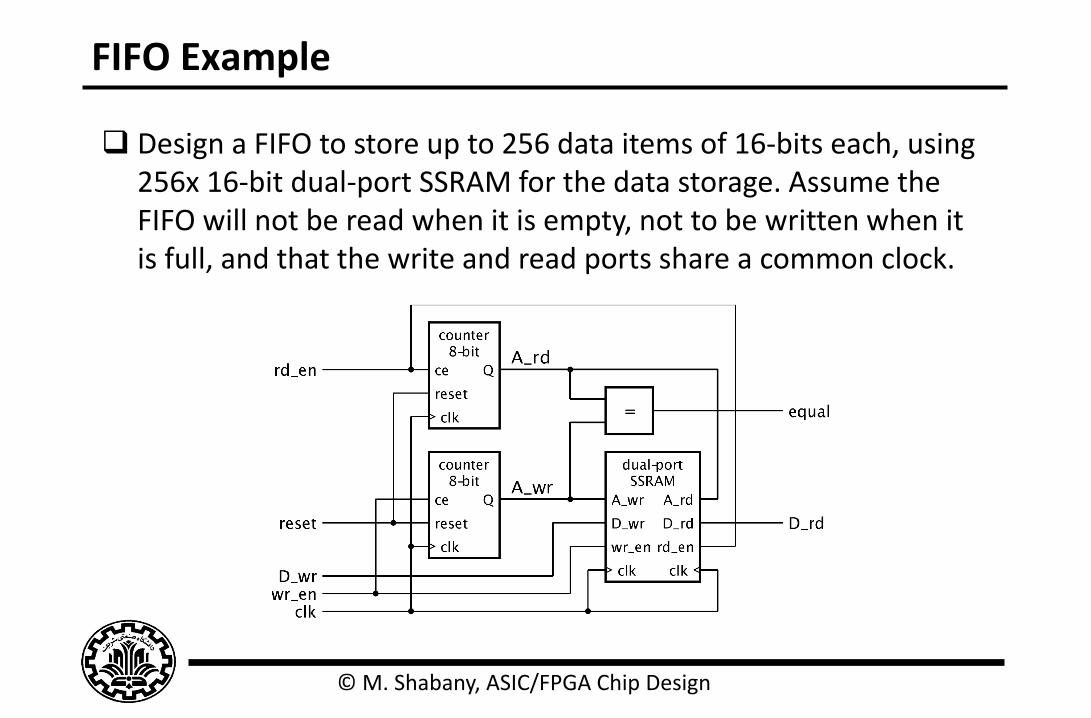
© M. Shabany, ASIC/FPGA Chip Design
FIFO Example
Design a FIFO to store up to 256 data items of 16-bits each, using 256x 16-bit dual-port SSRAM for the data storage. Assume the FIFO will not be read when it is empty, not to be written when it is full, and that the write and read ports share a common clock.
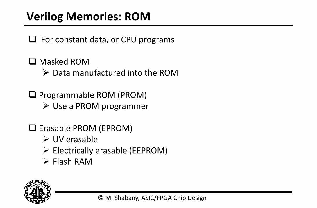
© M. Shabany, ASIC/FPGA Chip Design
Verilog Memories: ROM
For constant data, or CPU programs
Masked ROM Data manufactured into the ROM
Programmable ROM (PROM)
Use a PROM programmer
Erasable PROM (EPROM) UV erasable Electrically erasable (EEPROM) Flash RAM
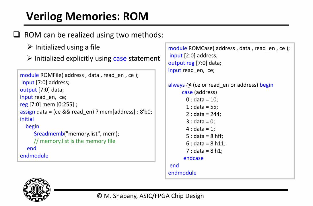
© M. Shabany, ASIC/FPGA Chip Design
Verilog Memories: ROM
ROM can be realized using two methods:
Initialized using a file
Initialized explicitly using case statement
module ROMFile( address , data , read_en , ce ); input [7:0] address; output [7:0] data; input read_en, ce; reg [7:0] mem [0:255] ; assign data = (ce && read_en) ? mem[address] : 8'b0; initial begin $readmemb("memory.list", mem); // memory.list is the memory file end endmodule
module ROMCase( address , data , read_en , ce ); input [2:0] address; output reg [7:0] data; input read_en, ce; always @ (ce or read_en or address) begin
case (address) 0 : data = 10; 1 : data = 55; 2 : data = 244; 3 : data = 0; 4 : data = 1; 5 : data = 8'hff; 6 : data = 8'h11; 7 : data = 8'h1; endcase
end endmodule

© M. Shabany, ASIC/FPGA Chip Design
Function Implementation using look-up tables
Complex or arbitrary functions are not uncommon Example:
always @ (input) begin case (input) 4’b0000: begin real=3’b100; imag=3’b001; end; 4’b0001: begin real=3’b000; imag=3’b101; end; 4’b0010: begin real=3’b110; imag=3’b011; end; …… default: begin real=3’bxxx; imag=3’bxxx; end; endcase end
One way is to implement it using Look-up Tables
Often best to write a Matlab program to write the Verilog table as plain text
Easy to adapt to other specifications Not efficient for very large tables Tables with data that is less random will
have smaller synthesized area
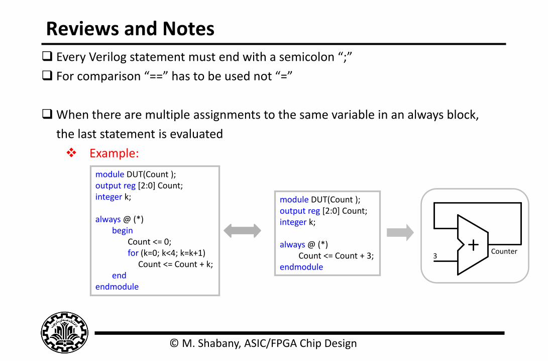
© M. Shabany, ASIC/FPGA Chip Design
Reviews and Notes Every Verilog statement must end with a semicolon “;”
For comparison “==” has to be used not “=”
When there are multiple assignments to the same variable in an always block,
the last statement is evaluated
Example:
module DUT(Count ); output reg [2:0] Count; integer k; always @ (*) begin
Count <= 0; for (k=0; k<4; k=k+1) Count <= Count + k;
end endmodule
module DUT(Count ); output reg [2:0] Count; integer k; always @ (*) Count <= Count + 3; endmodule
Counter3
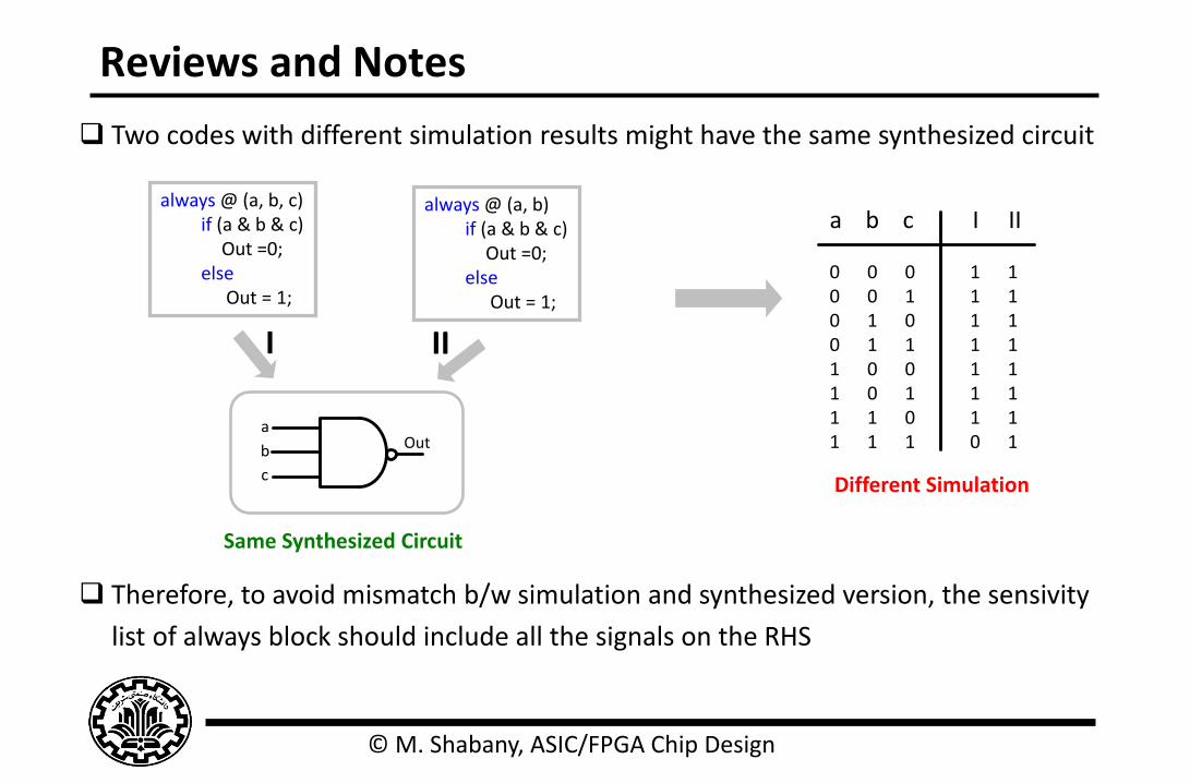
© M. Shabany, ASIC/FPGA Chip Design
Reviews and Notes
Two codes with different simulation results might have the same synthesized circuit
Therefore, to avoid mismatch b/w simulation and synthesized version, the sensivity
list of always block should include all the signals on the RHS
always @ (a, b, c) if (a & b & c)
Out =0; else
Out = 1;
always @ (a, b) if (a & b & c)
Out =0; else
Out = 1;
a b c I II
0 0 0 1 1 0 0 1 1 1 0 1 0 1 1 0 1 1 1 1 1 0 0 1 1 1 0 1 1 11 1 0 1 1 1 1 1 0 1Out
a
b
c
Same Synthesized Circuit
Different Simulation
I II
© M. Shabany, ASIC/FPGA Chip Design
Coding Styles
Do not mix blocking and non-blocking assignments in an always block
Use parentheses to optimize logic structure
Use meaningful names for signals, variables, and modules
Define if-else and case statements explicitly to avoid latch inference
Multiple procedural assignments (inside an always block) to a single variable is allowed.
The last assignment is evaluated.
Multiple continuous assignments (assign) to a single net in NOT allowed.
Do not mix edge and level sensitive elements together
Use assign statements for simple comb. logic and always block for complex comb. logic
Avoid mixing positive-edge and negative-edge triggered flip-flops in one design
Confuses the timing closure
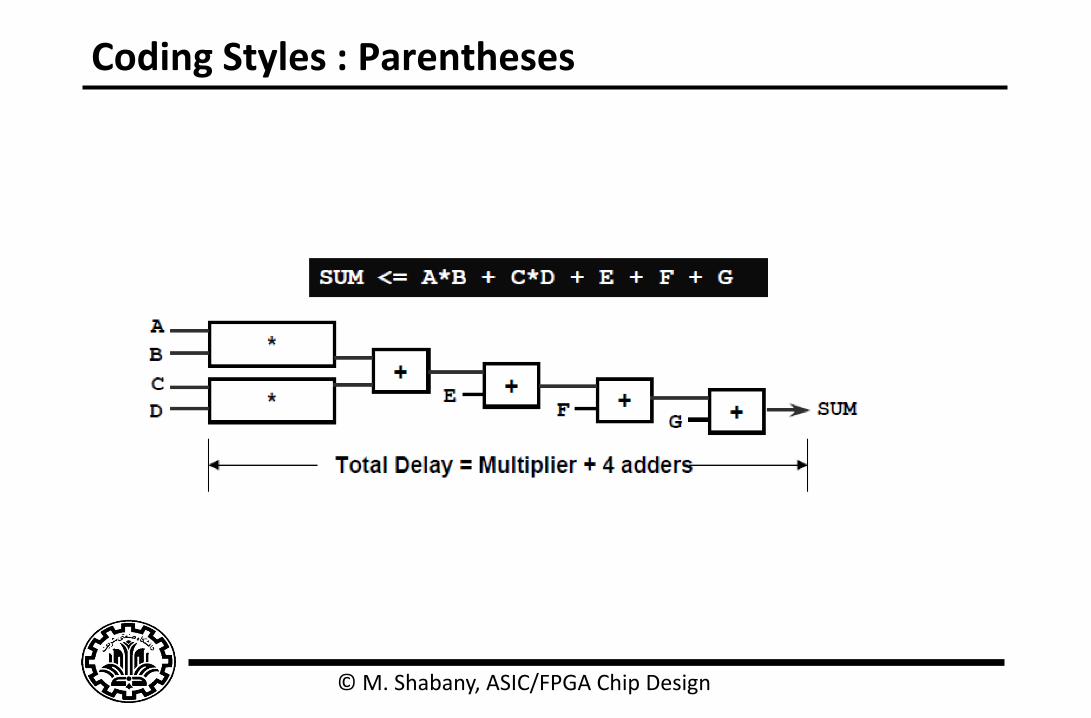
© M. Shabany, ASIC/FPGA Chip Design
Coding Styles : Parentheses

© M. Shabany, ASIC/FPGA Chip Design
Coding Styles : Parentheses
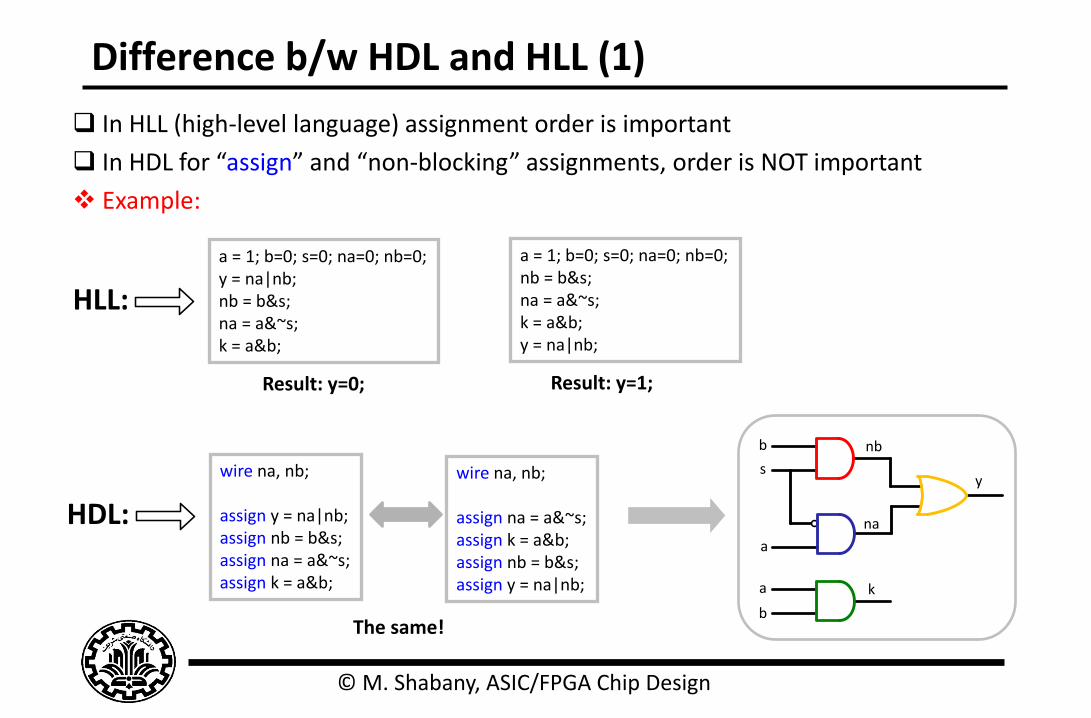
© M. Shabany, ASIC/FPGA Chip Design
Difference b/w HDL and HLL (1)
In HLL (high-level language) assignment order is important
In HDL for “assign” and “non-blocking” assignments, order is NOT important
Example:
a = 1; b=0; s=0; na=0; nb=0; y = na|nb; nb = b&s; na = a&~s; k = a&b;
a = 1; b=0; s=0; na=0; nb=0; nb = b&s; na = a&~s; k = a&b; y = na|nb;
Result: y=0; Result: y=1;
wire na, nb; assign y = na|nb; assign nb = b&s; assign na = a&~s; assign k = a&b;
wire na, nb; assign na = a&~s; assign k = a&b; assign nb = b&s; assign y = na|nb;
HLL:
HDL:
b
s
a
b
a
nb
na
y
k
The same!
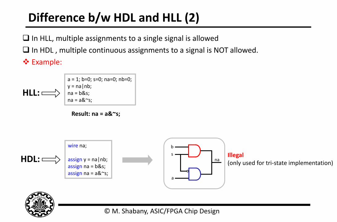
© M. Shabany, ASIC/FPGA Chip Design
Difference b/w HDL and HLL (2)
In HLL, multiple assignments to a single signal is allowed
In HDL , multiple continuous assignments to a signal is NOT allowed.
Example:
a = 1; b=0; s=0; na=0; nb=0; y = na|nb; na = b&s; na = a&~s;
Result: na = a&~s;
wire na; assign y = na|nb; assign na = b&s; assign na = a&~s;
HLL:
HDL:
b
s
a
naIllegal (only used for tri-state implementation)


![ASIC Design & FPGA-1st Chapter[1]](https://img.dokumen.tips/doc/110x75/577d203f1a28ab4e1e925961/asic-design-fpga-1st-chapter1.jpg)


