Embed Size (px)
Citation preview

AS1720 Soleno id / Va lve Dr iver w i th Current L imi tat ion
www.austriamicrosystems.com/Solenoid-Relay-Driver/AS1720 Revision 1.04 1 - 12
Datasheet
1 General Description
The AS1720A is a low side current source providing an optimized
DC Operation for power saving and ultra low electromagnetic
radiation.
The AS1720B is a low side switch providing a PWM output, which
frequency is defined by an internal RC oscillator. The adjustable
PWM allows a fine control of the power delivered to the load.
The AS1720A and AS1720B can be set to provide a strong initial
closure current and is automatically switching to hold mode for
power saving. The initial DC current, the hold current and the duty
cycle of the PWM can be adjusted by external resistors. An internal
thermal sensor prevents damage of the circuit due to excessive
heating up.
Both devices are optimized for driving electromechanical devices
such as valves, solenoids relays, actuators and positioners.
2 Key Features Supply Range: +5V to +50V
Internal VDDA: 3.3V
Supply Current: 1 mA
Internal osc frequency: 30kHz
Fix delay: 136ms
Adjustable duty cycle: 20% – 90% (AS1720B only)
Adjustable energizing current: 10mA – 100mA
Adjustable hold current: 30% - 70% of energizing current
Current Limitation
Thermal shutdown: 150ºC
8-pin MLPD (2x2mm) Package
On request SOIC 8 Package (reduced temperature range -40°C
to +85°C)
3 Applications
The AS1720 is ideal for fluid and gas flow systems, industrial control,
electrical heaters, motor speed control.
Table 1. Standard Products
Model Operation Mode
AS1720A DC Current Source Operation
AS1720B PWM Switching Operation
L
Energising Current adjust
Thermal Shutdown
PWM &Control
Free-Wheeling
Diode
Vsupply: +5V to +50V
IHENN IE
adjustable Duty cycle
Hold Current adjust
Internal VDDA typ. 3.3V
CurrentAdjust
LDO &Ref Generator
R1
R2Vref
100nF
RPU
OnOff
AS1720
Delay30kHz
Oscillator
VDDA
3
DUTY
2
VDDA
1
VDDHV
4
OUT
5
VSS
768
Figure 1. AS1720 - Block Diagram
RIE RIH
RL
10nF

www.austriamicrosystems.com/Solenoid-Relay-Driver/AS1720 Revision 1.04 2 - 12
AS1720
Datasheet - P in A s s ig n me n t s
4 Pin Assignments
Figure 2. Pin Out (Top View)
Pin Description
Table 2. Pin Descriptions
Pin Name Pin Number Description
VDDHV 1 Positive supply voltage
VDDA 2 Internal supply of 3.3V (typ.)
DUTY 3
Duty-Cycle. By means of this pin the duty cycle can be adjusted between 20% and 90% during hold
phase. The duty cycle can be adjusted by a voltage source or an external resistor divider. Setting this
pin to VDDA the 50% duty cycle is selected automatically.
OUT 4 Current Source Output
VSS 5 Ground
IE 6 Energize Current. This pin defines the current during energize phase by means of a resistor.
IH 7 Hold Current. This pin defines the current during hold phase by means of a resistor.
ENN 8
Enable Not. This pin can be used to switch on/off the current source (e.g. via a µP), when the
AS1720 is always powered on.
Low during start-up: When VDDHV is applied, the device starts with the energise phase, followed by
the hold phase.
When the device is constantly powered on, it can be controlled by this pin.
High: The output current source is switched off.
Low: The device starts with the energise phase, followed by the hold phase.
1VDDHV
AS17202VDDA
3DUTY
4OUT
8 ENN
7 IH
6 IE
5 VSS

www.austriamicrosystems.com/Solenoid-Relay-Driver/AS1720 Revision 1.04 3 - 12
AS1720
Datasheet - A b s o lu t e M a x i m u m R a t i n g s
5 Absolute Maximum Ratings
Stresses beyond those listed in Table 3 may cause permanent damage to the device. These are stress ratings only, and functional operation of
the device at these or any other conditions beyond those indicated in Section 6 Electrical Characteristics on page 4 is not implied. Exposure to
absolute maximum rating conditions for extended periods may affect device reliability.
Table 3. Absolute Maximum Ratings
Parameter Min Max Units Notes
Electrical Parameters
VDDHV, OUT -0.9 +55 V
VDDA, DUTY, ENN, IE, IH -0.3 +5 V
Input Current (latch-up immunity) -100 100 mA Norm: JEDEC 78 @85°C
Electrostatic Discharge
Electrostatic Discharge HBM +/- 1.5 kV Norm: MIL 883 E method 3015
Temperature Ranges and Storage Conditions
Thermal Resistance θJA +36 ºC/W
Junction Temperature TJ +140 ºC Internally limited
Storage Temperature Range -55 +150 ºC
Package Body Temperature +260 ºC
The reflow peak soldering temperature (body temperature) specified is in accordance with IPC/JEDEC J-STD-020 “Moisture/Reflow Sensitivity
Classification for Non-Hermetic Solid State Surface Mount Devices”.
The lead finish for Pb-free leaded packages is matte tin (100% Sn).
Humidity 5 85 % Non-condensing
Moisture Sensitive Level 1 Represents a max. floor life time of unlimited

www.austriamicrosystems.com/Solenoid-Relay-Driver/AS1720 Revision 1.04 4 - 12
AS1720
Datasheet - E le c t r i ca l C h a ra c t e r i s t i c s
6 Electrical Characteristics
VDDHV = 5V, VSS = 0V, Typical Values are at TAMB = +25ºC (unless otherwise specified). All limits are guaranteed. The parameters with min
and max values are guaranteed with production tests or SQC (Statistical Quality Control) methods.
Table 4. Electrical Characteristics
Symbol Parameter Conditions Min Typ Max Units
TAMB Operating Ambient Temperature -40 +85 °C
TJ Operating Junction Temperature -40 +125 °C
valid for AS1720A & AS1720B
VDDHV Supply Voltage Range 5 50 V
VDDA Internal Supply no load 3.1 3.3 3.5 V
IDD Supply Current 1 2 mA
IOUT_E Output Energizing Current Range1
1. The parameters are tested with proprietary test modes.
defined by RIE
(see Figure 10 on page 7)10 100 mA
VIHDigital Input Threshold @ pin ENN
2 VDDAV
VIL VSS 1.2
VHYST Hysteresis @ pin ENN 200 mV
RPU Pull-Up Resistor @ pin ENN 100 kΩ
Delay Time See Delay on page 6 136 ms
TSHDN Thermal Shutdown Temperature 160 ºC
∆TSHDN Thermal Shutdown Hysteresis 15 ºC
only valid for AS1720A
VOUT Saturation Voltage, Sink1 IOUT = 100mA 0.6 1 V
k Transfer ValueRIE = 12kΩ, VDDHV = 5V to 50V, OUT =
1V to 40V (see page 7)1080 1200 1320 AΩ
IOUT_H Output Hold Current Range1 defined by RIH
(see Figure 10 on page 7)0.3 x
IOUT_E0.7 x
IOUT_EmA
only valid for AS1720B
Minimum Duty Cycle 15 20 25 %
Maximum Duty Cycle 83 90 95 %
Internal Duty Cycle 50 %
VtrigTrigger level to select internal
voltage divider@ pin DUTY VDDA V
fPWM PWM Frequency 25.5 30 34.5 kHz
www.austriamicrosystems.com/Solenoid-Relay-Driver/AS1720 Revision 1.04 5 - 12
AS1720
Datasheet - Ty p i ca l O p e r a t i n g C h a r a c t e r i s t i c s
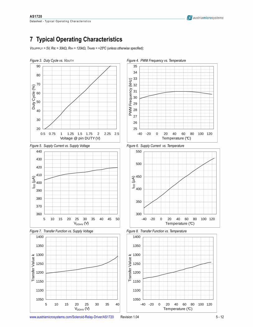
7 Typical Operating Characteristics
VSUPPLY = 5V, RIE = 30kΩ, RIH = 120kΩ, TAMB = +25ºC (unless otherwise specified);
Figure 3. Duty Cycle vs. VDUTY Figure 4. PWM Frequency vs. Temperature
20
30
40
50
60
70
80
90
0.5 0.75 1 1.25 1.5 1.75 2 2.25 2.5Voltage @ pin DUTY (V)
Dut
y C
ycle
(%
)
25
26
27
28
29
30
31
32
33
34
35
-40 -20 0 20 40 60 80 100 120Temperature (°C)
PW
M F
req
uen
cy (
kHz)
Figure 5. Supply Current vs. Supply Voltage Figure 6. Supply Current vs. Temperature
360
370
380
390
400
410
420
430
440
5 10 15 20 25 30 35 40 45 50VDDHV (V)
I DD (
µA
)
300
350
400
450
500
550
-40 -20 0 20 40 60 80 100 120Temperature (°C)
I DD (
µA
)
Figure 7. Transfer Function vs. Supply Voltage Figure 8. Transfer Function vs. Temperature
1050
1100
1150
1200
1250
1300
1350
1400
5 10 15 20 25 30 35 40VDDHV (V)
Tra
nsfe
r V
alu
e k
1050
1100
1150
1200
1250
1300
1350
1400
-40 -20 0 20 40 60 80 100 120Temperature (°C)
Tra
nsfe
r V
alu
e k

www.austriamicrosystems.com/Solenoid-Relay-Driver/AS1720 Revision 1.04 6 - 12
AS1720
Datasheet - D e t a i l e d D e s c r i p t i o n
8 Detailed Description
DelayThe delay time is generated internally by a digital divider.
LDO and Reference GeneratorThis block provides the internal supply voltage of typ. 3.3V and all bias currents for the analog cells. Further the external resistor divider for
setting the duty cycle will be supplied.
Thermal shutdownThe temperature is constantly monitored. If the temperature exceeds typ. 160ºC the output is disabled. In order to exit the over temperature
condition, the device has to cool down and the reason of over temperature (e.g. short circuit) must be removed. After exiting the overtemperature
condition the system restarts beginning with the energizing phase followed by the hold phase.
DC Operation (AS1720A only)After power up, the delay time (see Delay) starts running. After expiration of the delay the hold phase starts automatically. During the hold phase
the DC output current is reduced according to the RIH on pin IH.
PWM Operation (AS1720B only)After power up, the delay time (see Delay) starts running. After expiration of the delay the hold phase starts automatically. The internal RC
oscillator sets the PWM period. The duty cycle is either defined by the external resistor divider (voltage) at pin DUTY or by the fixed internal
divider. When using the external divider the duty cycle can be adjusted between 20% and 90% (e.g. from a DAC). Alternatively the pin can be
driven by a voltage source. For using the internal divider the pin DUTY has to be connected to VDDA. The comparator recognizes this condition
and switches to the internal divider, which causes a fixed 50% duty cycle.
Figure 9. Simplified Circuit of Block PWM and Control
(EQ 1)DUTYCYCLE VDUTY( ) 0 381, VDUTY× 0 014,–=
DUTY
adjustable Duty cycle
fixed50% Duty cycle
optional
PWM &Control
DUTY
30kHzOscillator
VDDA
R1
R2Vref
RPU
ENN
OnOff
Internal VDDA typ. 3.3V
Delay
VDDA
VDDA

www.austriamicrosystems.com/Solenoid-Relay-Driver/AS1720 Revision 1.04 7 - 12
AS1720
Datasheet - D e t a i l e d D e s c r i p t i o n
Control by pin ENNWhen VDDHV is constantly switched on the AS1720 can be controlled by pin ENN. The functionality is the same as for controlling the device via
pin VDDHV. This feature is useful when controlling by a microprocessor is desired.
Because of the internal pull-up resistor to VDDA a microprocessor with open-drain or with push/pull (max 3.3V) output can be used.
Current Adjust (AS1720A) and Current Limitation (AS1720B) This block provides the current reference for the output current source. The current is generated by regulating the internal Bandgap voltage to
the pins IE and IH. The external resistors RIE and RIH define the output current and can be expressed as:
The temperature coefficient depends on the Bandgap voltage (100ppm/K, box method) and external resistor (in the range of several ppm/K).
The saturation voltage of the output current source for a 100mA current is typical 600mV.
Figure 10. Simplified Circuit of Blocks Current Adjust and Current Source
(EQ 2)RIE IH⁄k
IOUT------------=
Current mirror1.2V reference
IE
RIE
1.2V
OUT
RIH
IH
PWM & Control

www.austriamicrosystems.com/Solenoid-Relay-Driver/AS1720 Revision 1.04 8 - 12
AS1720
Datasheet - A p p l i c a t i o n I n f o r m a t i o n
9 Application Information
In order to drive relays, which need more than 100mA current, an external circuitry (see Figure 11) can be used. This application shows how to
drive 5W @12V relays.
This circuit is only applicable for AS1720A.
For this example with R1 = 100Ω and RS = 2.5Ω the current Is is calculated as follows:
Figure 11. AS1720A - Typical Application
(EQ 3)IS I1
R1
RS------× 0 01A, 100
2 5,---------× 400mA===
BC161
100Ω
LM741
IS
Relay
VDDHV
Vsupply: +12V
IHENN
DUTY
IE
VSS
OUT
VDDA
100nF
AS1720A I1
1VR1
RS
10mA
RIE
120kΩ
+
-
Free-Wheeling
Diode
RIH
240kΩ
Energising Current adjust Hold Current adjust

www.austriamicrosystems.com/Solenoid-Relay-Driver/AS1720 Revision 1.04 9 - 12
AS1720
Datasheet - P a c k a g e D ra w i n g s a n d M a r k i n g s
10 Package Drawings and Markings
Figure 12. 8-pin MLPD (2x2mm) Marking

www.austriamicrosystems.com/Solenoid-Relay-Driver/AS1720 Revision 1.04 10 - 12
AS1720
Datasheet - P a c k a g e D ra w i n g s a n d M a r k i n g s
Figure 13. 8-pin MLPD (2x2mm) Package

www.austriamicrosystems.com/Solenoid-Relay-Driver/AS1720 Revision 1.04 11 - 12
AS1720
Datasheet - O r d e r i n g I n f o r ma t i o n
11 Ordering Information
The device is available as the standard products shown in Table 5.
Note: All products are RoHS compliant and austriamicrosystems green. Buy our products or get free samples online at ICdirect: http://www.austriamicrosystems.com/ICdirect Technical Support is found at http://www.austriamicrosystems.com/Technical-Support For further information and requests, please contact us mailto:[email protected] or find your local distributor at http://www.austriamicrosystems.com/distributor
Table 5. Ordering Information
Ordering Code Marking Description Delivery Form Package
AS1720A-ATDT A0Solenoid / Valve Driver with Current Limitation and with
DC Current Source OperationTape and Reel 8-pin MLPD (2x2mm)
AS1720B-ATDT AWSolenoid / Valve Driver with Current Limitation and with
PWM Switching OperationTape and Reel 8-pin MLPD (2x2mm)

www.austriamicrosystems.com/Solenoid-Relay-Driver/AS1720 Revision 1.04 12 - 12
AS1720
Datasheet
Copyrights
Copyright © 1997-2011, austriamicrosystems AG, Tobelbaderstrasse 30, 8141 Unterpremstaetten, Austria-Europe. Trademarks Registered ®.
All rights reserved. The material herein may not be reproduced, adapted, merged, translated, stored, or used without the prior written consent of
the copyright owner.
All products and companies mentioned are trademarks or registered trademarks of their respective companies.
Disclaimer
Devices sold by austriamicrosystems AG are covered by the warranty and patent indemnification provisions appearing in its Term of Sale. aus-
triamicrosystems AG makes no warranty, express, statutory, implied, or by description regarding the information set forth herein or regarding the
freedom of the described devices from patent infringement. austriamicrosystems AG reserves the right to change specifications and prices at
any time and without notice. Therefore, prior to designing this product into a system, it is necessary to check with austriamicrosystems AG for
current information. This product is intended for use in normal commercial applications. Applications requiring extended temperature range,
unusual environmental requirements, or high reliability applications, such as military, medical life-support or life-sustaining equipment are specif-
ically not recommended without additional processing by austriamicrosystems AG for each application. For shipments of less than 100 parts the
manufacturing flow might show deviations from the standard production flow, such as test flow or test location.
The information furnished here by austriamicrosystems AG is believed to be correct and accurate. However, austriamicrosystems AG shall not
be liable to recipient or any third party for any damages, including but not limited to personal injury, property damage, loss of profits, loss of use,
interruption of business or indirect, special, incidental or consequential damages, of any kind, in connection with or arising out of the furnishing,
performance or use of the technical data herein. No obligation or liability to recipient or any third party shall arise or flow out of
austriamicrosystems AG rendering of technical or other services.
Contact Information
Headquarters
austriamicrosystems AG Tobelbaderstrasse 30 A-8141 Unterpremstaetten, Austria
Tel: +43 (0) 3136 500 0 Fax: +43 (0) 3136 525 01
For Sales Offices, Distributors and Representatives, please visit:
http://www.austriamicrosystems.com/contact


![Leuetatze 4/15 [pdf, 2.25 MB]](https://img.dokumen.tips/doc/110x75/588470351a28abf9188c0344/leuetatze-415-pdf-225-mb.jpg)


