Embed Size (px)
Citation preview

Application of Genetic OptimizationAlgorithms to Lumped Circuit
Modelling of Coupled Planar CoilsJens Werner1, Lars Nolle1, Jennifer Schutt2
1 Jade University of Applied Science Wilhelmshaven/Oldenburg/Elsfleth,Friedrich-Paffrath-Str. 101, D-26389 Wilhelmshaven,Email: [email protected], [email protected]
2 Nexperia Germany GmbH, Stresemannallee 101, D-22529 HamburgEmail: [email protected]
KEYWORDS
Coupled planar coils; Common mode filter; Lumpednetwork model; Genetic algorithm; SPICE model
ABSTRACT
In portable electronic devices, like smart phones, cou-pled planar coils are often used as common mode filters(CMF). The purpose of these CMF is to suppress elec-tromagnetic interference (EMI) between wireless com-munications systems (e.g. WIFI) and digital high-speed interfaces (e.g. USB 3). A designer of such anelectronic device usually carries out a signal integrity(SI) analysis, using models of the system components.There are two alternative ways of modelling the CMF:One is based on matrices (called S-parameters) that de-scribe the behaviour in the frequency domain and areeither derived from measurements or simulation tools.The other is using a representation based on lumpedcircuit networks. In this work, a lumped network is gen-erated manually based on expert knowledge. The ad-vantage of this approach is the reduced number of onlypassive network components compared to traditionalmethods that produce much larger networks compris-ing of many active and passive devices. On the otherhand, suitable component values of the lumped networkneed to be found so that the network exhibits the samefrequency response as the physical device. Since thereare many interacting parameters to be tuned, this can-not be achieved manually. Hence, a genetic algorithmis applied to this optimisation problem. Two sets ofexperiments were carried out and a sensitivity analy-sis has been conducted. It has been shown that theproposed method is capable of finding near optimal so-lutions within reasonable computation time.
INTRODUCTION
Modern portable electronic devices have to be ascompact as possible whilst being efficient. In such de-vices, miniaturized planar coils can be found, for ex-ample, in common mode filters which are built directlyinto integrated circuits.
For the design of these coils, sophisticated simulation
tools based on the method of moments (Keysight, 2016;Harrington, 1968) are often used. Usually, these simu-lations return frequency dependent scattering parame-ters (S-parameters, (Pozar, 2012)). This is a black-boxapproach describing the electrical behaviour in the fre-quency domain at the ports (or: terminals) of the de-vice without revealing details about the physics of theinternal structure (1).
[S] =
Sdd,11 Sdd,12 Sdc,11 Sdc,12
Sdd,21 Sdd,22 Sdc,21 Sdc,22
Scd,11 Scd,12 Scc,11 Scc,12
Scd,21 Scd,22 Scc,21 Scc,22
(1)
In matrix (1) all elements are complex valued andfrequency dependent. The two parameters Sdd,21 andScc,21 describe the transmission characteristics betweenthe two ports for two different modes of operation, dif-ferential mode (dd) and common mode (cc). Thoseparameters with mixed indices (Sdc,ij and Scd,ij) arerelevant for the conversion from one mode to another;for that reason the elements of matrix (1) are also calledmixed-mode S-parameters (Bockelman and Eisenstadt,1995). For passive and reciprocal devices the forwardand reverse transmission parameters Sx,21 and Sx,12
are identical. The focus in this work is on Sdd,21 andScc,21, which are the most important parameters forreal world applications.
Fig. 1 shows the two modes of operation for a two-port device, like a CMF. The two ports are denoted bythe indices 1 and 2 as used in (1). In differential mode(Fig. 1 a)) opposing currents (I+, I−) are applied to thepins of port 1. There is no current in the ground path(Ignd = 0). The transfer characteristics of this modefrom port 1 to port 2 is described by Sdd,21.
In common mode (Fig. 1 b)), the pins of port 1 aredriven commonly, resulting in a return current of thesame amplitude in the ground path. The transfer char-acteristics of this mode from port 1 to port 2 is de-scribed by Scc,21.
However, sometimes a designer needs to analyse thebehaviour in the time domain as well. Here, an equiva-lent circuit model is usually required, which exhibits the
Proceedings 31st European Conference on Modelling and Simulation ©ECMS Zita Zoltay Paprika, Péter Horák, Kata Váradi, Péter Tamás Zwierczyk, Ágnes Vidovics-Dancs, János Péter Rádics (Editors) ISBN: 978-0-9932440-4-9/ ISBN: 978-0-9932440-5-6 (CD)

Sdd,21
DUTI = I+ 0
I = I- 0
I = 0gnd
Port 1 Port 2
GND
Scc,21
DUTI = I / 2+ 0
I = I / 2- 0
I = Ignd 0
Port 1 Port 2
GND
a) b)
Fig. 1. Differential mode and common mode currents of a two-port device under test (DUT).
same characteristics as the coil in both, the time andthe frequency domain. In general, broadband SPICEgenerators (Simulation Program with Integrated Cir-cuit Emphasis) produce networks of idealised compo-nents (so called lumped networks), which exhibit therequired behaviour at their terminals (Stevens andDhaene, 2008). In practice, these networks consist of alarge number of active and passive components, whichdo not resemble the physics of the coils. The approachpresented in this paper uses expert knowledge to gen-erate a network which is closer to the actual physicswhilst being much smaller. The challenge in this ap-proach is that the component values of this networkhave to be determined. However, even for networkswith few components the search space is too vast tofind the optimum values manually. Therefore, a com-putational optimisation approach is used in this workand applied to a common mode filter (CMF) that con-sists of two planar coupled coils.
APPLICATION
In high-speed differential data lines (e.g. USB,SATA, PCIe) the spectrum used overlaps with wirelessradio communication bands (e.g. GSM, LTE, WIFI).Electromagnetic interference (EMI) for example causedby USB 3 data lines can potentially disturb wireless ap-plications in the 2.4 GHz band as reported in (Intel,2012; Chen et al., 2013; USB, 2016). In the same man-ner, the spectrum of an USB 2 signal might interferewith the GSM 900 MHz downlink spectrum (Werneret al., 2015). This can cause a degradation of the re-ceiver sensitivity in a mobile phone.
As wireless and wired signals utilise the same fre-quency band, a low pass filter can not be used to reduceunwanted interference from data lines into an antennaand finally the receiver. Instead, a common mode filteris applied. The purpose of a CMF is to suppress un-wanted common mode (CM) currents on the data lines,since those currents are responsible for the EMI. Ide-ally, the differential mode (DM) currents of the wantedhigh-speed signals are not affected. Typically, CMFsare built using two coupled coils.
Common mode filter with on-chip planar coils
Fig. 2 a) shows the top view on a planar copper coilas part of an integrated on-chip CMF (Werner et al.,2016). In addition Fig. 2 b) presents the layout viewfrom the EM design tool (Keysight, 2016).
For all kind of digital high-speed transmission sys-
Fig. 2. Planar top view: a) die photograph; b) layout in EMtool (Werner et al., 2016).
tems, a signal integrity (SI) analysis is performed inthe time domain. This involves the simulation of a largenumber of transmitted data bits and the evaluation oftheir electrical characteristics at each sampling pointin the time domain. The segmented and overlappedrepresentation of this time domain data is known aseye diagram (Gao et al., 2010; Ahmadyan et al., 2015).Here, the simulation in the time domain benefits froman exact and compact SPICE model of the involvedplanar structures.
Circuitry
The fundamental common mode filtering is achievedby two planar copper coils. The chosen device-under-test (DUT) provides furthermore ESD protection in or-der to avoid destruction of the sensitive CMOS system-on-chip (SoC). This protection is accomplished by twolow-voltage triggered semiconductor controlled recti-fiers (LVTSCR) which will shunt the current of anESD pulse into the ground (GND) connection. TheseLVTSCR are depicted by the diode symbols in Fig. 3.In an real application, like a smart phone with USB 3connector, the diodes would be mounted towards theexternal interface, in order to protect the SuperSpeedreceive (SSRX) or transmit (SSTX) signal lines.
Fig. 3. Functional diagram (Werner et al., 2016).
Physical realisation
The filter device is fabricated in a planar bipolarsemiconductor process with two metal layers made byaluminium. In addition, three layers of polyimide andthree layers of copper are added on top of the planarwafer. Two of these copper layers form the planarcoupled coils. There is no plastic package surround-ing the silicon die, instead the device is attached withsolder balls and manufactured as wafer level chip scalepackage. The contact side of the CMF is depicted inFig. 2 a). The five solder balls marked with ”Port”,”SOC” and ”GND” can be clearly identified as well as
the octagonal shaped coil around the GND ball. Thelayout of this CMF, generated in an EM simulationtool, is shown in Fig. 2 b). It marks in the same man-ner the five ball pads. Due to the top view perspectiveonly the upper coil layer can be seen.
Fig. 4. Cross sectional view from EM simulation tool showingall metal layers (without solder balls) (Werner et al., 2016).
Fig. 5. Cross sectional view from scanning electron microscope:a) symmetric cut through GND ball; b) detailed view on upperand lower copper coil layer (Werner et al., 2016).
The cross sectional view in Fig. 4 provides a moredetailed perspective into the structure:
The symbol ”A” marks the top level metal of thesemiconductor process which is needed to implementthe basic semiconductor schematic. Furthermore it pro-vides the interconnection to the 3-metal/3-polyimide-process. ”B” denotes the interconnect between firstcopper layer and top aluminium layer. ”C” and ”D”mark the two copper layers which are the core of thiscommon mode filter. These layers determine domi-nantly the inductance and resistance of the coils. Thethird copper layer, marked by ”E”, enables the so-calledunder bump metal, a drop area for the solder ball.
Fig. 5 depicts the physical cross section of the man-ufactured CMF. Fig. 5 a) shows a cross section that isorthogonal to the cut plane as shown in Fig. 4. Thispicture gives a good impression about the real relationbetween silicon thickness, solder ball and copper struc-tures. As it can be seen in Fig. 5 b) the planar coilwindings are rectangular shaped with a larger widththan height and a spacing in the same range as theheight. The typical spacing between the coil windingsis 5 µm.
STRUCTURAL MODELLING
As mentioned above, when a designer needs to ana-lyse the behaviour of an entire system in the timedomain, for example for a signal integrity analysis, alumped network can offer a solution. In contrast totransforming S-parameters directly into the time do-main, this approach has the advantage that causality,
passivity and reciprocity (Triverio et al., 2007) are in-herently fulfilled.
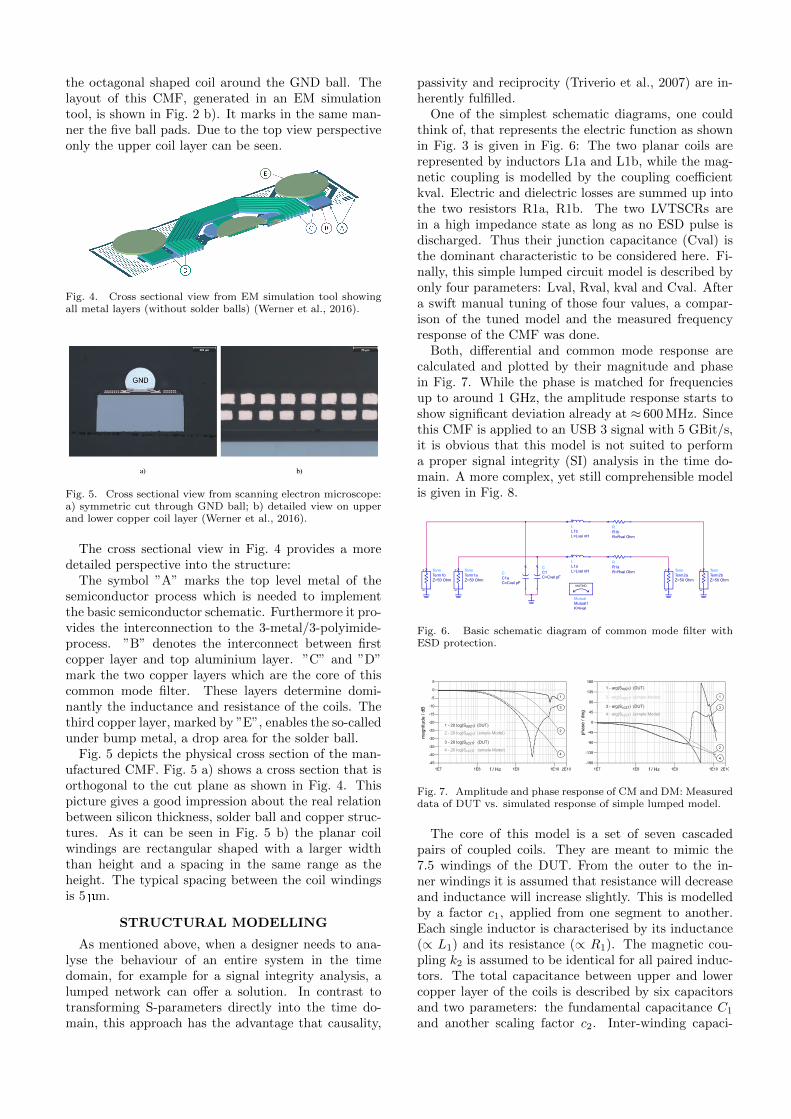
One of the simplest schematic diagrams, one couldthink of, that represents the electric function as shownin Fig. 3 is given in Fig. 6: The two planar coils arerepresented by inductors L1a and L1b, while the mag-netic coupling is modelled by the coupling coefficientkval. Electric and dielectric losses are summed up intothe two resistors R1a, R1b. The two LVTSCRs arein a high impedance state as long as no ESD pulse isdischarged. Thus their junction capacitance (Cval) isthe dominant characteristic to be considered here. Fi-nally, this simple lumped circuit model is described byonly four parameters: Lval, Rval, kval and Cval. Aftera swift manual tuning of those four values, a compar-ison of the tuned model and the measured frequencyresponse of the CMF was done.
Both, differential and common mode response arecalculated and plotted by their magnitude and phasein Fig. 7. While the phase is matched for frequenciesup to around 1 GHz, the amplitude response starts toshow significant deviation already at ≈ 600 MHz. Sincethis CMF is applied to an USB 3 signal with 5 GBit/s,it is obvious that this model is not suited to performa proper signal integrity (SI) analysis in the time do-main. A more complex, yet still comprehensible modelis given in Fig. 8.
MUTIND
C
L R
C
Mutual
L R
TermTerm TermTermL1a
C1a
R1aC1
Mutual1
L1b R1b
Term2aTerm1a Term2bTerm1b C=Cval pF
L=Lval nH
C=Cval pF
R=Rval Ohm
K=kval
L=Lval nH
Z=50 OhmZ=50 Ohm Z=50 OhmZ=50 Ohm
R=Rval Ohm
Fig. 6. Basic schematic diagram of common mode filter withESD protection.
1E8 1E9 1E10 01E27E1
-40
-35
-30
-25
-20
-15
-10
-5
0
-45
5
f / Hz
mag
nitu
de /
dB
1E8 1E9 1E10 01E27E1
-135
-90
-45
0
45
90
135
-180
180
f / Hz
phas
e / d
eg
1 - 20 log(S ) (DUT)dd21
4 - 20 log(S ) (simple Model)cc21
3 - 20 log(S ) (DUT)cc21
2 - 20 log(S ) (simple Model)dd21
2 - arg(S ) (simple Model)dd21
1 - arg(S ) (DUT)dd21
4 - arg(S ) (simple Model)cc21
3 - arg(S ) (DUT)cc21
1
2
3
4
1
2
3
4
Fig. 7. Amplitude and phase response of CM and DM: Measureddata of DUT vs. simulated response of simple lumped model.
The core of this model is a set of seven cascadedpairs of coupled coils. They are meant to mimic the7.5 windings of the DUT. From the outer to the in-ner windings it is assumed that resistance will decreaseand inductance will increase slightly. This is modelledby a factor c1, applied from one segment to another.Each single inductor is characterised by its inductance(∝ L1) and its resistance (∝ R1). The magnetic cou-pling k2 is assumed to be identical for all paired induc-tors. The total capacitance between upper and lowercopper layer of the coils is described by six capacitorsand two parameters: the fundamental capacitance C1
and another scaling factor c2. Inter-winding capaci-

MUTIND
MUTIND MUTIND MUTIND MUTIND MUTIND MUTIND
R
R
RMutual
L
L
LL
LL L
LL
L
L
L
L
LL
L
L
L
L
L
CC
C
C
TermTerm
TermTerm
Mutual Mutual Mutual Mutual Mutual Mutual
R3
R1
R2Mutuald
L3a
L3b
L5aL4a
Lb7Lb5Lb4L L6b
L7aL6a
Loutb
Louta
L2b
L2a
bdLadL
Lgnd
L1b
L1a
Linb
Lina
CdbCda
C7
C14
Term2aTerm1a
Term2bTerm1b
Mutual_L2 Mutual_L3 Mutual_L4 Mutual_L5 Mutual_L6 Mutual_L7
R=damp
R=Rsval Ohm
R=Rsval Ohm
MUTIND
MutualMutual_L1K=k2
K=k1
R=RdoutVal OhmL=LdoutVal nH
R=RdoutVal OhmL=LdoutVal nH
R=Rdval OhmL=Ldval nH
R=Rdval OhmL=Ldval nH
R=Rgnd OhmL=Lgndval pH
R=R1val OhmL=L1val nH
R=RdinVal OhmL=LdinVal nH
R=RdinVal OhmL=LdinVal nH
C=C1val pFC=C1val pF
C=Csval pF
C1C
Fp lav1pC=C
CC2C=c Cp1val pF1
2.
CC3C=c Cp1val pF2
2.
CC4C=c Cp1val pF3
2.
CC5C=c Cp1val pF4
2.
CC6C=c Cp1val pF5
2.
C=Csval pF
Z=50 OhmZ=50 Ohm
Z=50 OhmZ=50 Ohm
R=(R1val / c ) OhmL=c L1val nH.1
11
1R=(R1val / c ) OhmL=c L1val nH.2
2
1
1
R=(R1val / c ) OhmL=c L1val nH.3
3
1
1
R=(R1val / c ) OhmL=c L1val nH.4
4
1
1
R=(R1val / c ) OhmL=c L1val nH.5
5
1
1
R=(R1val / c ) OhmL=c L1val nH.6
6
1
1
R=R1val OhmL=L1val nH
R=(R1val / c ) OhmL=c L1val nH.1
11
1R=(R1val / c ) OhmL=c L1val nH.2
2
1
1
R=(R1val / c ) OhmL=c L1val nH.3
3
1
1
R=(R1val / c ) OhmL=c L1val nH.4
4
1
1
R=(R1val / c ) OhmL=c L1val nH.5
5
1
1
R=(R1val / c ) OhmL=c L1val nH.6
6
1
1
K=k2 K=k2 K=k2 K=k2 K=k2 K=k2
Fig. 8. Lumped element circuit diagram as used in the simulation and optimisation process.
tance is neglected. Cross-talk from the CMF input tothe output is modelled by a series network Cs, Rs oneach signal line. In general the impedance of each signaltrace at the terminals is modelled by a series resistorand inductor. The values of these components (Lin, Rin
and Lout, Rout) may differ for input and output sincethe LVTSCRs are only present at one side. For thejunction capacitance of the LVTSCRs the capacitanceCd is used. The impedance of the inter-connect metalis modelled by Ld, Rd while the shunt resistor Rds rep-resents losses and is applied to tune the quality fac-tor of the LC-circuit formed by Lc and Cd. Finally,the connection to the GND ball is defined by Lgnd andRgnd. The challenge now is to determine the 19 compo-nent values so that the behaviour of the lumped modelmatches that of the measurements from the actual de-vice. This is achieved in this work by computationaloptimisation.
MODEL OPTIMISATION
In computational optimisation a given error functionf is driven towards an extreme value by a direct searchalgorithm in an iterative process (see Fig. 9). The errorfunction maps an error value onto a given design vectord. Here, this vector contains the 19 component valuesto be optimised (2).
The error e is then used by the optimisation algo-rithm to create new candidate solutions, i.e. designvectors.
The challenge in this research is to find an optimumdesign vector d′ that produces a DM and CM frequencyresponse as close as possible to the measured data ofthe DUT by minimising the error function (3).
d = {Lin, Rin, Ld, Rd, k1, Rds, · · · , Lout, Rout}T (2)
d′ = arg min f(d) (3)
The error function and the algorithm used in thiswork are described below.
Error Function
OptimisationAlgorithm
d e = f( )d
Fig. 9. Optimisation loop
Error function
For the problem at hand the error is defined as dif-ference between a calculated and a measured frequencyresponse (5)-(13). Such a difference can be calculatedby comparing both graphs at arbitrary discrete fre-quencies. Since the given frequency responses exhibita strong variation at rather high frequencies, the sam-pling rates have been chosen differently for low and highfrequencies according to (4), see Fig. 10.
Since the interest is in both, differential mode andcommon mode response, two error terms eDM and eCM
are combined using the weighted sum (5).
Both frequency responses are complex valued, i.e.amplitude and phase have to be optimised. With (6)and (10) again a weighted sum is used to combine thesecontributions to the error value.

f (i) =
10 MHz ·(
10110
)i∀ 0 ≤ i ≤ 27, i ∈ N
5 GHz ·(
10192
)i−27∀ 28 ≤ i ≤ 62, i ∈ N
(4)
1x10 7 1x10 8 1x10 9 1x10 10 1x10 11
f / Hz
Fig. 10. Spacing of the 63 discrete frequency points for the errorfunction.
e =1
2· eDM +
1
2· eCM (5)
eDM =62∑i=0
10 · emagDM (i) + ephaseDM (i) (6)
ephaseDM (i) =∣∣∣arg
(SDUTdd,21(f(i))
)− arg
(Soptdd,21(f(i))
)∣∣∣(7)
emagDM (i) =
{5 ·∆mag
DM (i) if i < 54 ∧ ∆magDM (i) ≥ 0.1
1 ·∆magDM (i) else
(8)
∆magDM (i) =
∣∣∣∣∣20 · log
(∣∣∣∣∣SDUTdd,21(f(i))
Soptdd,21(f(i))
∣∣∣∣∣)∣∣∣∣∣ (9)
eCM =62∑i=0
10 · emagCM (i) + ephaseCM (i) (10)
ephaseCM (i) =∣∣arg
(SDUTcc,21 (f(i))
)− arg
(Soptcc,21(f(i))
)∣∣(11)
emagCM (i) =
{2 ·∆mag
CM (i) if i < 81 ·∆mag
CM (i) else(12)
∆magCM (i) =
∣∣∣∣∣20 · log
(∣∣∣∣∣SDUTcc,21 (f(i))
Soptcc,21(f(i))
∣∣∣∣∣)∣∣∣∣∣ (13)
Computational Optimisation
For engineering design optimisation, it is recom-mended to use a fixed number of decimal places (Nolleet al., 2016). Thus, the optimisation problem wastransformed into a discrete optimisation problem. Forthis, a genetic algorithm (GA) (Goldberg, 1989) wasused to minimise the error function (Fig. 9).
Genetic algorithms are discrete optimisation algo-rithms which simulate the evolutionary mechanismfound in nature by using heredity and mutation. Theywere first introduced in 1975 by Holland (Holland,1975) who also provided a theoretical framework forgenetic algorithms, the Schemata Theorem.
For the optimisation problem under consideration,an integer coded genetic algorithm (Abbas, 2006) was
used. Fig. 11 shows the chromosome structure em-ployed.
Lin Rin Ld Rd ... Ls Cs Lout Rout1 2 3 4 16 17 18 19
Fig. 11. Chromosome structure used.
Each gene holds integer numbers from the range1...2000 and is decoded into its phenotype by multi-plication with a scaling factor and addition of an offsetvalue in order to represent the fractional componentvalues of the network. This results in a lower limit andan upper limit for the search space of each componentvalue as listed in Table I.
Start
Stop
Select pm, pc, n, r, imax
i < ?
i := 0
Print best result
Select n parents using r tournaments
Apply crossover with probability pc
Apply mutation with probability pm
Replace parents with better offspring
i := i + 1Randomly initialise gene pool
imax
Fig. 12. Flowchart of the genetic algorithm used.
Fig. 12 shows a flowchart of the basic algorithm. Af-ter choosing the mutation probability pm, the crossoverprobability pc, the number n of individuals in the genepool, the number r of tournaments used for the se-lection of one parent, and the maximum number ofiterations imax, the gene pool is randomly initialised.In each of the n generations, parents from the currentgeneration are selected for the mating pool using tour-nament selection with r tournaments each (Miller andGoldberg, 1996). Then, uniform crossover (Syswerda,1989) is used with probability pc to produce offspringfrom the mating pool. After power mutation (Deepand Thakur, 2007) is applied to the offspring with theprobability pm, parents that perform worse than theiroffspring are replaced by their offspring. The algorithmterminates after imax generations.
The next section provides the results of the experi-ments conducted.

TABLE I: Optimisation parameters and results of the second simulation set with N = 25 runs
Parameter 1 2 3 4 5 6 7 8 9 10 11 12 13 14 15 16 17 18 19
Name Lin Rin Ld Rd k1 Rds Cd Lgnd Rgnd L1 R1 k2 c1 Cp c2 Rs Cs Lout Rout
unit nH Ohm nH Ohm 1 kOhm pF pH Ohm nH Ohm 1 1 pF 1 Ohm pF nH OhmLower limit 0.5 0.0 1.0 2.0 -1.0 2.0 0.0 200 3.0 1.0 0.0 0.4 1.0 0.0 0.6 100 0.0 0.5 3.0Upper limit 2.5 2.0 7.0 14.0 -0.4 4.0 2.0 600 5.0 7.0 2.0 1.0 1.8 2.0 1.0 500 2.0 2.5 9.0
EXPERIMENTS
For the experiments, the number of generationswas set to imax = 20,000 and the population size ton = 1000. The crossover probability was chosen to bepc = 0.6 and the mutation probability was pm = 0.001.Five individuals competed in each tournament. Allthese parameters were determined empirically and havebeen applied successfully in previous work (Werner andNolle, 2016). With respect to the search space of theoptimisation variables, two sets of experiments wereconducted, each with 25 simulation runs.
The error values are normalized by the lower boundof the error values, i.e. 880. Fig. 13 shows a conver-gence plot for the average errors and the best solutionsof each generation over 25 runs. It can be observed thatmost populations have converged after approximately4000 generations.
After the first set of 25 runs it could be observedthat 14 runs ended with an Lout value of 0 nH, which isexactly the lower limit of this optimisation parameter.The solutions related to this result are labelled group I.The other eleven solutions, denoted group II, resultedin 0.7 nH< Lout <1.3 nH. Results for both groups andthe measured data are shown in Fig. 14. Even thoughthe group I solutions yield a lower error value thanthose of group II they show a rather large deviation inthe magnitude against the response of the DUT. Sincethe response of group II is more desirable and the valueof Lout = 0 nH is physically unreasonable, the lowerlimit for this parameter was adjusted to 0.5 nH for thesecond set of 25 runs.
After the adjustment of the lower limit for Lout aclustering could still be observed; solutions belongingto one cluster converged towards the (new) lower limitwhereas the others converged towards 1.15 nH. There-fore, the solutions were analysed separately for eachcluster (Table II). Both clusters of this second set werelabelled group I and II in the same way as it was donein the first set: Group I solutions are the ones that con-verged towards the lower limit of Lout, the remainingsolutions belong to group II.
DISCUSSION
The best solution of group II (Table II) was used asoverall solution and compared with the measurementdata. Fig. 15 and Fig. 16 depict the frequency responsesfor both, the differential and the common mode, of thesimulation respectively the measured data.
Fig. 15 shows that, for the differential mode, ampli-tude |Sdd,21| and phase arg(Sdd,21) are matched verywell up to approximately 7 GHz. At the resonance fre-quency of 7.6 GHz, amplitude and phase show a certain
1
2
3
4
5
6 7 8 9
10
1 10 100 1000 10000 100000
norm
aliz
ed e
rror
generations
best in generation
average of gene pool
Fig. 13. Convergence plot of 25 optimisation runs. The errorvalue is normalized by 880.
-3.0
-2.5
-2.0
-1.5
-1.0
-0.5
0.0
1x10⁷ 1x10⁸ 1x10⁹ 1x10¹⁰
group I solutions
group II solutionsreference (DUT)
f / Hz
mag
nitu
de /
dB
20 log(S ) dd21
Fig. 14. Differential mode frequency response of DUT and resultsof first optimisation run. Two groups of local optima can beidentified.
deviation and above 9 GHz the model and measure-ments do not agree. For the common mode (Fig. 16)the amplitude response |Scc,21| is matched quite well ingeneral with the exception of the resonance frequencyaround 2.5 GHz and frequencies above 5 GHz.
The phase arg(Scc,21) is matched accurately up to600 MHz. At higher frequencies it still follows the mea-surements in principle, but with a higher error.
For both modes, the chosen model matches the mea-surements well in amplitude and phase over wide fre-quency ranges. This can be observed in more detailfrom Fig. 17, which shows the logarithmic magnitude ofthe complex differences. For frequencies below 7 GHzboth differences are below -20 dB.
In order to analyse the complexity of this optimisa-tion problem, a sensitivity analysis of the componentvalues has been performed. In the optimum solutionfrom group II (best (II) in Table II) each element of theoptimum design vector d′ is varied one at a time by astep of (h ·d′i) with h = 1 ·10−3. This allows to approx-imate the derivative of the error function with respect

TABLE II: Optimisation parameters and results of the second simulation set with N = 25 runs
Parameter 1 2 3 4 5 6 7 8 9 10 11 12 13 14 15 16 17 18 19
Name Lin Rin Ld Rd k1 Rds Cd Lgnd Rgnd L1 R1 k2 c1 Cp c2 Rs Cs Lout Rout
unit nH Ohm nH Ohm 1 kOhm pF pH Ohm nH Ohm 1 1 pF 1 Ohm pF nH Ohm
Best (I) 0.96 1.01 3.10 2.01 -.86 2.24 0.07 494 3.06 4.27 0.03 0.87 1.06 0.19 0.86 233 0.05 0.50 3.10Mean (I) 0.81 0.55 4.38 2.97 -.66 3.17 0.06 318 3.03 3.58 0.09 0.84 1.13 0.15 0.89 239 0.06 0.89 3.53Std. dev. (I) 0.26 0.41 0.45 1.43 0.06 0.34 0.01 98 0.06 0.69 0.08 0.02 0.06 0.02 0.03 13 0.00 0.42 0.42
Best (II) 0.60 0.45 4.10 2.02 -.60 2.60 0.06 210 3.01 2.65 0.01 0.82 1.22 0.13 0.90 226 0.06 1.12 3.78Mean (II) 0.60 0.48 4.45 2.24 -.63 3.04 0.06 312 3.02 2.76 0.07 0.82 1.20 0.13 0.91 227 0.06 1.15 3.59Std. dev.(II) 0.08 0.28 0.32 0.48 0.04 0.27 0.00 125 0.02 0.17 0.05 0.00 0.02 0.01 0.02 5 0.00 0.16 0.31
1E8 1E9 1E10 01E27E1
-8
-6
-4
-2
-10
0
-150
-100
-50
0
50
100
150
-200
200
f / Hz
mag
nitu
de /
dB phase / deg
20 log(S ) (DUT)dd21
20 log(S ) (Model)dd21
arg(S ) (Model)dd21
arg(S ) (DUT)dd21
Fig. 15. Differential mode frequency response Sdd,21 of DUTand model.
1E8 1E9 1E10 01E27E1
-30
-20
-10
-40
0
-80
-60
-40
-20
0
20
40
-100
60
f / Hz
mag
nitu
de /
dB phase / deg
20 log(S ) (DUT)cc21
20 log(S ) (Model)cc21
arg(S ) (Model)cc21
arg(S ) (DUT)cc21
Fig. 16. Common mode frequency response Scc,21 of DUT andmodel.
to the ith component of d (Bischof and Carle, 1998).
∂f(d)
∂di
∣∣∣∣d=d′
≈ f(d′ + h · d′i · ei)− f(d′)
h · d′i(14)
Here, f is the error function and ei is the ith Carte-sian basis vector. The analysis is done for both errorfunctions of the differential and the common mode.
Table III presents the sensitivities for the commonmode (CM sens.) and the differential mode (DM sens.)for each component. It can be observed that some sensi-tivities are equal or close to zero, i.e with respect to thecorresponding parameter, a (local) optimum has beenreached, whereas others show a significant deviationfrom zero. This indicates that further improvementsmight be possible.
Another interesting aspect is that in the commonmode there is no electric current through components6, 14 and 15, meaning that their respective componentvalues are irrelevant. Likewise in differential mode,
1E8 1E9 1E10 01E27E1
-45
-40
-35
-30
-25
-20
-15
-10
-5
-50
0
f / Hzer
ror v
ecto
r mag
nitu
de /
dB
20 log( |S (DUT) - S (Model)| )dd21 dd21
20 log( |S (DUT) - S (Model)| )cc21 cc21
Fig. 17. Error vector magnitude for differential and commonmode frequency response comparing DUT and model.
TABLE III: Sensitivity analysis of the component values of the
optimum solution from group II.
Nr Comp. CM sens. DM sens.1 Lin -355.5 290.92 Rin -6.5 2.43 Ld -0.1 350.94 Rd 3.4 -0.85 k1 -1.3 -987.36 Rds 0.0 -0.017 Cd -2418.6 28330.88 Lgnd 0.0 0.09 Rgnd 6.7 0.010 L1 39.2 -264.211 R1 -30.1 1.912 k2 67.0 -353.713 c1 313.1 -324.414 Cp 0.0 -5829.715 c2 0.0 -281.316 Rs -0.4 0.217 Cs 2041.2 -707.818 Lout -89.1 -748.319 Rout -7.6 0.9
no current is traversing through components 8 and 9,hence they have no effect on the resulting frequencyresponses. Both observations agree with the actualphysics of the network.
CONCLUSION AND FUTURE WORK
In this work, the behaviour of a coupled coil devicewas modelled by a lumped element network. The ad-vantage is that this model describes the device not onlyin the frequency domain, but also in the time domain.The latter is important for the signal integrity analy-sis of high-speed interfaces, like USB 3. The topologyof the network was generated manually using expertknowledge. It should be noted that the modelling of acomplex physical device by a simplified (lumped) net-

work can never achieve an exact representation but onlya close approximation. The challenge of this approachis that the component values of the network have to bedetermined.
The aim is to find a local optimum which producesa frequency response as close as possible to the DUTcharacteristic.
Since this optimisation problem is complex, a com-putational optimisation method, namely a genetic al-gorithm, was employed. The solution found producedgood matching between the measurements and modelresponses for frequencies up to approximately 7 GHz.Whilst this agreement would be sufficient for many ap-plications it is not adequate enough to be applied tointerfaces with data rates of 5 Gbit/s and above. Thisis due to the fact that the fifths harmonic of the funda-mental wave of the signal (5·2.5 GHz) is of importance.
The fact that the results were clustered into twogroups indicates that the global optimum was notfound. This assumption is support by the results fromthe sensitivity analysis presented here.
The next stage of this research will foucs on threedifferent aspects: tuning the error function, adjustingthe GA control parameters and testing alternative op-timisation algorithms.
Bluetooth & USB 3.0 - A guide to resolvingyour Bluetooth woes, 2016. URL http://
www.bluetoothandusb3.com/. [2017-03-30].H. M. Abbas. Accurate resolution of signals using
integer-coded genetic algorithms. In 2006 IEEE In-ternational Conference on Evolutionary Computa-tion, pages 2888–2895, July 2006.
S. N. Ahmadyan, C. Gu, S. Natarajan, E. Chiprout,and S. Vasudevan. Fast eye diagram analysis for high-speed CMOS circuits. In 2015 Design, AutomationTest in Europe Conference Exhibition (DATE), pages1377–1382, March 2015.
Christian Bischof and Alan Carle. Automatic differenti-ation principles, tools, and applications in sensitivityanalysis. In Second International Symposium on Sen-sitivity Analysis of Model Output, pages 33–36, April1998. ISBN 92-828-3498-0.
D. E. Bockelman and W. R. Eisenstadt. Combineddifferential and common-mode scattering parameters:theory and simulation. IEEE Transactions on Mi-crowave Theory and Techniques, 43(7):1530–1539,July 1995. ISSN 0018-9480.
C. H. Chen, P. Davuluri, and D. H. Han. A novelmeasurement fixture for characterizing USB 3.0 radiofrequency interference. In Electromagnetic Compat-ibility (EMC), 2013 IEEE International Symposiumon, pages 768–772, Aug. 2013.
Kusum Deep and Manoj Thakur. A new mutation oper-ator for real coded genetic algorithms. Applied Math-ematics and Computation, 193(1):211–230, 2007.
W. Gao, L. Wan, S. Liu, L. Cao, D. Guidotti, J. Li,Z. Li, B. Li, Y. Zhou, F. Liu, Q. Wang, J. Song, H. Xi-
ang, J. Zhou, X. Zhang, and F. Chen. Signal integritydesign and validation for multi-GHz differential chan-nels in SiP packaging system with eye diagram pa-rameters. In Electronic Packaging Technology HighDensity Packaging (ICEPT-HDP), 2010 11th Inter-national Conference on, pages 607–611, Aug. 2010.
David E. Goldberg. Genetic Algorithms in Search, Op-timization and Machine Learning. Addison-WesleyLongman Publishing Co., Inc., Boston, MA, USA,1st edition, 1989. ISBN 0201157675.
R. F. Harrington. Field Computation by Moment Meth-ods. The Macmillan Company, 1968.
J.H. Holland. Adaptation in natural and artificial sys-tems. 1975.
Intel. USB 3.0* Radio Frequency InterferenceImpact on 2.4 GHz Wireless Devices, 2012.URL http://www.intel.com/content/dam/www/public/us/en/documents/white-papers/usb3-
frequency-interference-paper.pdf. [2017-03-30].Keysight. ADS - Advanced Design System, 2016. URLhttp://www.keysight.com/find/eesof-ads. [2017-03-30].
B. L. Miller and David E. Goldberg. Genetic algo-rithms, tournament selection, and the effect of noise.Complex Systems, (9):193–212, 1996.
Lars Nolle, R. Krause, and R. J. Cant. On practicalautomated engineering design. In K. Al-Begain andA. Bargiela, editors, Seminal Contributions to Mod-elling and Simulation. Springer, 2016.
David M. Pozar. Microwave engineering. J. Wiley &Sons, 4th edition, 2012. ISBN 978-0-470-63155-3.
N. Stevens and T. Dhaene. Generation of rationalmodel based spice circuits for transient simulations.In 2008 12th IEEE Workshop on Signal Propagationon Interconnects, pages 1–4, May 2008.
Gilbert Syswerda. Uniform crossover in genetic algo-rithms. In J. David Schaffer, editor, ICGA, pages2–9. Morgan Kaufmann, 1989. ISBN 1-55860-066-3.
P. Triverio, S. Grivet-Talocia, M. S. Nakhla, F. G.Canavero, and R. Achar. Stability, causality, and pas-sivity in electrical interconnect models. IEEE Trans-actions on Advanced Packaging, 30(4):795–808, Nov.2007. ISSN 1521-3323.
J. Werner, J. Schutt, and G. Notermans. Sub-miniaturecommon mode filter with integrated ESD protection.In 2015 IEEE International Symposium on Electro-magnetic Compatibility (EMC), pages 386–390, Aug.2015.
J. Werner, J. Schutt, and G. Notermans. Commonmode filter for USB 3 interfaces. In 2016 IEEE In-ternational Symposium on Electromagnetic Compati-bility (EMC), pages 100–104, July 2016.
Jens Werner and Lars Nolle. Spice Model Generationfrom EM Simulation Data Using Integer Coded Ge-netic Algorithms. In Max Bramer and Miltos Petridis,editors, 2016 SGAI, pages 355–367. Springer Interna-tional Publishing, Dec. 2016.
REFERENCES