Embed Size (px)
Citation preview
Trans. Nonferrous Met. Soc. China 22(2012) 1801−1809
Application of EBSD technique to ultrafine grained and
nanostructured materials processed by severe plastic deformation: Sample preparation, parameters optimization and analysis
CHEN Yong-jun, Jarle HJELEN, Hans J. ROVEN
Department of Materials Science and Engineering, Norwegian University of Science and Technology,
NO-7491, Trondheim, Norway
Received 10 November 2011; accepted 25 June 2012
Abstract: With the help of FESEM, high resolution electron backscatter diffraction can investigate the grains/subgrains as small as a few tens of nanometers with a good angular resolution (~0.5°). Fast development of EBSD speed (up to 1100 patterns per second) contributes that the number of published articles related to EBSD has been increasing sharply year by year. This paper reviews the sample preparation, parameters optimization and analysis of EBSD technique, emphasizing on the investigation of ultrafine grained and nanostructured materials processed by severe plastic deformation (SPD). Detailed and practical parameters of the electropolishing, silica polishing and ion milling have been summarized. It is shown that ion milling is a real universal and promising polishing method for EBSD preparation of almost all materials. There exists a maximum value of indexed points as a function of step size. The optimum step size depends on the magnification and the board resolution/electronic step size. Grains/subgrains and texture, and grain boundary structure are readily obtained by EBSD. Strain and stored energy may be analyzed by EBSD. Key words: electron backscatter diffraction (EBSD); sample preparation; parameters optimization; step size; severe plastic deformation (SPD) 1 Introduction
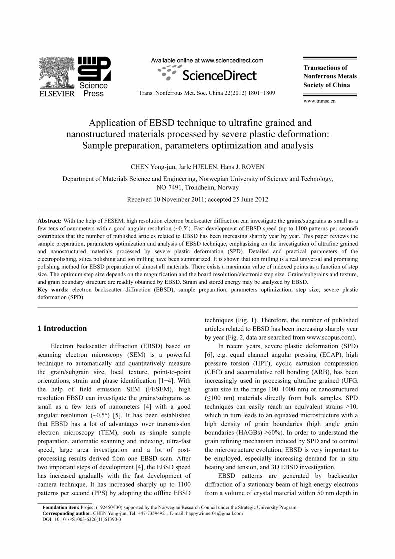
Electron backscatter diffraction (EBSD) based on scanning electron microscopy (SEM) is a powerful technique to automatically and quantitatively measure the grain/subgrain size, local texture, point-to-point orientations, strain and phase identification [1−4]. With the help of field emission SEM (FESEM), high resolution EBSD can investigate the grains/subgrains as small as a few tens of nanometers [4] with a good angular resolution (~0.5°) [5]. It has been established that EBSD has a lot of advantages over transmission electron microscopy (TEM), such as simple sample preparation, automatic scanning and indexing, ultra-fast speed, large area investigation and a lot of post- processing results derived from one EBSD scan. After two important steps of development [4], the EBSD speed has increased gradually with the fast development of camera technique. It has increased sharply up to 1100 patterns per second (PPS) by adopting the offline EBSD
techniques (Fig. 1). Therefore, the number of published articles related to EBSD has been increasing sharply year by year (Fig. 2, data are searched from www.scopus.com).
In recent years, severe plastic deformation (SPD) [6], e.g. equal channel angular pressing (ECAP), high pressure torsion (HPT), cyclic extrusion compression (CEC) and accumulative roll bonding (ARB), has been increasingly used in processing ultrafine grained (UFG, grain size in the range 100−1000 nm) or nanostructured (≤100 nm) materials directly from bulk samples. SPD techniques can easily reach an equivalent strains ≥10, which in turn leads to an equiaxed microstructure with a high density of grain boundaries (high angle grain boundaries (HAGBs) ≥60%). In order to understand the grain refining mechanism induced by SPD and to control the microstructure evolution, EBSD is very important to be employed, especially increasing demand for in situ heating and tension, and 3D EBSD investigation.
EBSD patterns are generated by backscatter diffraction of a stationary beam of high-energy electrons from a volume of crystal material within 50 nm depth in
Foundation item: Project (192450/I30) supported by the Norwegian Research Council under the Strategic University Program Corresponding author: CHEN Yong-jun; Tel: +47-73594921; E-mail: [email protected] DOI: 10.1016/S1003-6326(11)61390-3
CHEN Yong-jun, et al/Trans. Nonferrous Met. Soc. China 22(2012) 1801−1809
1802
Fig. 1 Collected patterns per second as function of year
Fig. 2 Published articles related to EBSD as function of year the specimen [3,7]. Therefore, the sample preparation is extremely crucial. This paper is concerned with the sample preparation, parameters optimization and results analysis. 2 Sample preparation
Despite a number of recommended preparation methods are available on internet, in publications or books, detailed and practical information about the preparation parameters is still missing. In general, almost all samples for EBSD observation need to be mechanically polished carefully. The suggested steps based on the experience in our group for the mechanical polishing sequence are listed in Table 1. When preparing soft materials (e.g. pure Al and its alloys), it is recommended to grind with a soap coating on SiC paper to avoid deep scratches or being embedded by hard particles. The grinding/polishing force depends on the hardness of materials, and less force is normally used with softer materials. Some materials such as magnesium alloys should never touch water after the last step listed in Table 1.
Table 1 Basic mechanical polishing sequence
Step Method Lubricant Time
1 80 grit SiC paper Water Until plane
2 600 grit SiC paper Water 20−90 s
3 1200 grit SiC paper Water 20−90 s
4 2400 grit SiC paper Water 20−90 s
5 6 μm diamond solution Ethanol 1−5 min
6 3 μm diamond solution Ethanol 1−5 min
7 1 μm diamond solution Ethanol 1−5 min
Normally, the samples cannot be used for EBSD after 1 μm diamond polishing. There are three main methods (electropolishing, silica polishing and ion milling) for the final polishing of EBSD samples to achieve good quality of patterns. 2.1 Electropolishing
Electropolishing is a popular polishing method for the final step of EBSD preparation. It is one of the most effective methods for samples processed by SPD because it removes the microstrain induced by mechanical polishing. Electropolishing is a process by which surface material is removed from the sample by passage of electric current while the sample is made an anode (or positive terminal) in a designed solution.
In general, the fresh surface which is easy to oxidize is recommended to be electropolished below room temperature. Sample preparation for some materials like Mg alloys, which is known to be very difficult, should be performed carefully. EBSD observation should be done immediately followed by electropolishing due to the easy oxidation on free surface.
The electropolishing parameters of some commonly used materials are listed in Table 2. It can be seen that almost all materials require a subzero temperature to avoid the oxidizing problem. The electrolytes of AC2 and A3 are the product names of Struers Company. More information can be found from Ref. [8]. Normally, the electrolytes that are used to produce TEM thin foils can be used on electropolishing of bulk specimens [9]. For some materials like magnesium alloys, it is very useful to have an additional mechanical polishing with diluted OPS solution just before electropolishing [10].
The quality of the polished surface is controlled by some parameters, e.g. voltage, temperature, flow rate and polishing time. It is important to note that some solutions have a short shelf life [9]. The common problems, possible causes and the actions during electropolishing, are listed in Table 3 [15]. Although Table 3 is an instruction manual for the electropolishing machine of Lectropol-5 made by Struers Company, it works to shoot most problems during electropolishing.

CHEN Yong-jun, et al/Trans. Nonferrous Met. Soc. China 22(2012) 1801−1809
1803
Table 2 Summary of electropolishing parameters of some commonly used materials
Material Electrolyte Voltage/V Polishing time/s Temperature/°C Ref.
AZ31 Mg alloy AC2 15 10−15 −30 [10]
Pure Ti A3 40 15−25 −30 [12]
Al alloys 20% perchloric acid and 80% ethanol 20 25 −30 [11]
Steel 5% (volume fraction) perchloric acid 40 − −40 [13]
Nb single crystal 30 mL HF+40 mL H2SO4+130 mL lactic acid 20 120 −5 [14]
Table 3 Common problems, possible causes and actions during electropolishing [15]
Problem Possible cause Action
Surface not polished or only partly polished
1. Current density insufficient; 2. Electrolyte used;
3. Insufficient quantity of electrolyte
1. Increase voltage to get higher current; 2. Renew electrolyte;
3. Add electrolyte
Spots that have not been polished
1. Gas bubbles/voltage too high; 2. Gas/bubbles/ flow rate too high; 3. Electrolyte temperature too high
1. Decrease the voltage; 2. Adjust flow rate;
3. Check electrolyte temperature
Polished surface is etched
1. Chemical attack of the grain boundaries after switching off the current;
2. Voltage too low
1. Remove and clean the specimen immediately after current is switched off;
2. Increase voltage
Pitting 1. Time too long;
2. Voltage too high; 3. Insufficient anodic layer
1. Improve preparation prior to polishing; 2. Decrease the time;
3. Decrease the voltage; 4. Decrease the flow rate
Deposits on surface Insoluble reaction products 1. Use a different electrolyte or a freshly mixed one; 2. Increase the voltage
Wavy surface
1. Time too short; 2. Flow rate not correct;
3. Electrolyte used; 4. Selective polishing because of different phases;
5. Wrong electrolyte; 6. Unsuitable preparation
1. Increase the time; 2. Try to decrease/or increase the flow rate;
3. Replace the electrolyte; 4. Improve preparation prior to polishing;
5. Use different electrolyte with other polishing area; 6. Improve the preparation prior to polishing
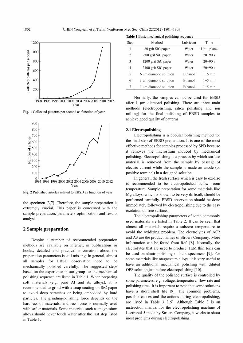
Figure 3 shows the EBSD orientation maps with
successful electropolishing on light metals before and after SPD [1,2,10]. It is well known that the pattern quality of the EBSD deteriorates with increasing density of defects like dislocations and accumulated strain in materials processed by SPD. Therefore, the microstructures without SPD (Figs. 3(a) and (c)) can be easily characterized by EBSD and the image quality (IQ) is very high. Materials processed by SPD are very difficult to be investigated by EBSD and, therefore sometimes non-indexed points (black points) present in the heavily deformed area (Fig. 3(d)). In general, the electropolishing parameters that work for materials processed by SPD can be used for the same material without SPD. The materials with higher atomic number like nickel and steel can yield stronger Kikuchi patterns, thus the sample preparation is not so critical. However,
the sample preparation for Al−Mg alloys (low atomic number) processed by SPD, especially for high magnesium content, is very difficult. In this case, short annealing at low temperature could be a nice way to improve the pattern quality [11]. 2.2 Silica polishing
Electropolishing works very well for EBSD preparation of many samples. However, there is no universal electrolyte working for all materials and the non-conductive materials cannot be prepared by electropolishing. As a solution working for nearly all materials, colloidal sillica is a commercially available solution which consists of negatively charged particles of silicon dioxide (SiO2) with a pH value between 8 and 11 [9]. When polishing with this solution, the sample surface is slightly etched and the deformation layer
CHEN Yong-jun, et al/Trans. Nonferrous Met. Soc. China 22(2012) 1801−1809
1804
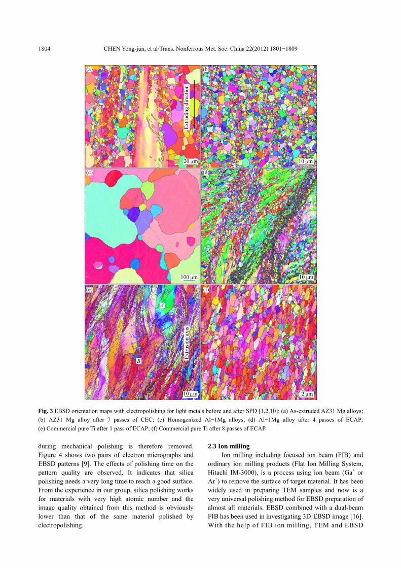
Fig. 3 EBSD orientation maps with electropolishing for light metals before and after SPD [1,2,10]: (a) As-extruded AZ31 Mg alloys; (b) AZ31 Mg alloy after 7 passes of CEC; (c) Homogenized Al−1Mg alloys; (d) Al−1Mg alloy after 4 passes of ECAP; (e) Commercial pure Ti after 1 pass of ECAP; (f) Commercial pure Ti after 8 passes of ECAP during mechanical polishing is therefore removed. Figure 4 shows two pairs of electron micrographs and EBSD patterns [9]. The effects of polishing time on the pattern quality are observed. It indicates that silica polishing needs a very long time to reach a good surface. From the experience in our group, silica polishing works for materials with very high atomic number and the image quality obtained from this method is obviously lower than that of the same material polished by electropolishing.
2.3 Ion milling Ion milling including focused ion beam (FIB) and
ordinary ion milling products (Flat Ion Milling System, Hitachi IM-3000), is a process using ion beam (Ga+ or Ar+) to remove the surface of target material. It has been widely used in preparing TEM samples and now is a very universal polishing method for EBSD preparation of almost all materials. EBSD combined with a dual-beam FIB has been used in investigating 3D-EBSD image [16]. With the help of FIB ion milling, TEM and EBSD
CHEN Yong-jun, et al/Trans. Nonferrous Met. Soc. China 22(2012) 1801−1809
1805
Fig. 4 Two image pairs showing electron micrographs and EBSD patterns and effects of polishing time on pattern quality observed [9]: (a, a′) 10 min colloidal silica, pattern IQ of 25; (b, b′) 30 min colloidal silica, pattern IQ of 166 investigations can be completed in the same area of the same sample [17].
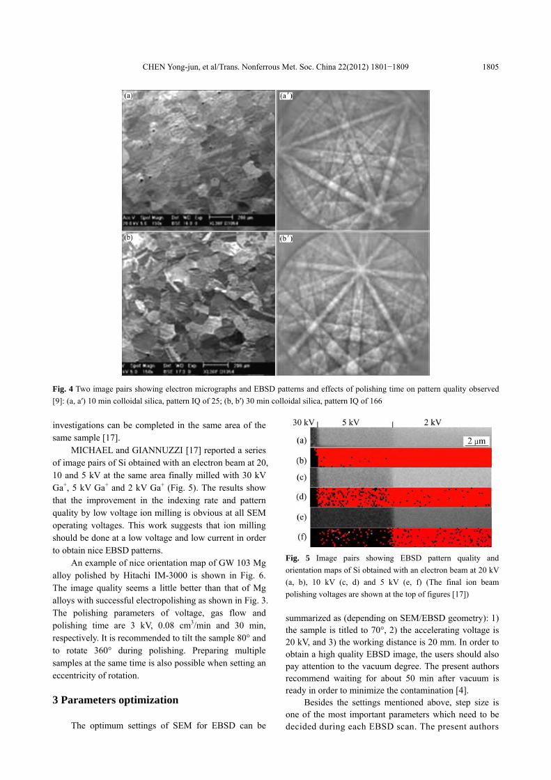
MICHAEL and GIANNUZZI [17] reported a series of image pairs of Si obtained with an electron beam at 20, 10 and 5 kV at the same area finally milled with 30 kV Ga+, 5 kV Ga+ and 2 kV Ga+ (Fig. 5). The results show that the improvement in the indexing rate and pattern quality by low voltage ion milling is obvious at all SEM operating voltages. This work suggests that ion milling should be done at a low voltage and low current in order to obtain nice EBSD patterns.
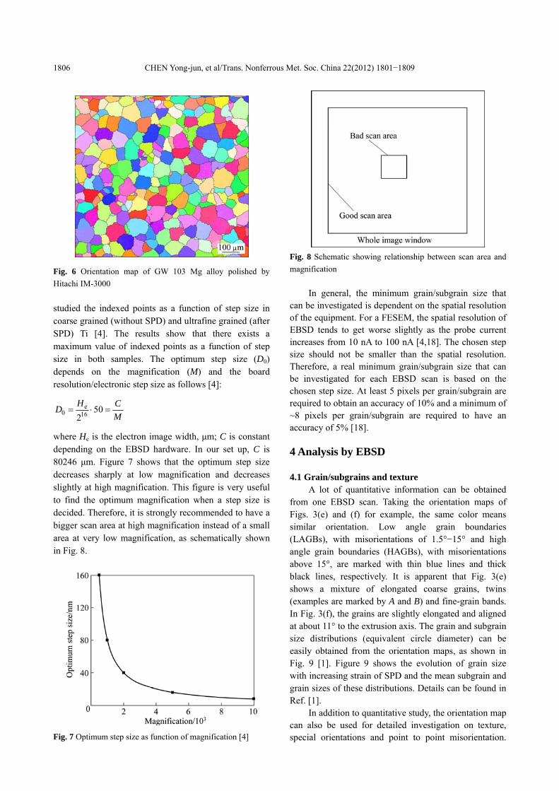
An example of nice orientation map of GW 103 Mg alloy polished by Hitachi IM-3000 is shown in Fig. 6. The image quality seems a little better than that of Mg alloys with successful electropolishing as shown in Fig. 3. The polishing parameters of voltage, gas flow and polishing time are 3 kV, 0.08 cm3/min and 30 min, respectively. It is recommended to tilt the sample 80° and to rotate 360° during polishing. Preparing multiple samples at the same time is also possible when setting an eccentricity of rotation. 3 Parameters optimization
The optimum settings of SEM for EBSD can be
Fig. 5 Image pairs showing EBSD pattern quality and orientation maps of Si obtained with an electron beam at 20 kV (a, b), 10 kV (c, d) and 5 kV (e, f) (The final ion beam polishing voltages are shown at the top of figures [17]) summarized as (depending on SEM/EBSD geometry): 1) the sample is titled to 70°, 2) the accelerating voltage is 20 kV, and 3) the working distance is 20 mm. In order to obtain a high quality EBSD image, the users should also pay attention to the vacuum degree. The present authors recommend waiting for about 50 min after vacuum is ready in order to minimize the contamination [4].
Besides the settings mentioned above, step size is one of the most important parameters which need to be decided during each EBSD scan. The present authors
CHEN Yong-jun, et al/Trans. Nonferrous Met. Soc. China 22(2012) 1801−1809
1806
Fig. 6 Orientation map of GW 103 Mg alloy polished by Hitachi IM-3000 studied the indexed points as a function of step size in coarse grained (without SPD) and ultrafine grained (after SPD) Ti [4]. The results show that there exists a maximum value of indexed points as a function of step size in both samples. The optimum step size (D0) depends on the magnification (M) and the board resolution/electronic step size as follows [4]:
e
0 16 502H CD
M= ⋅ =
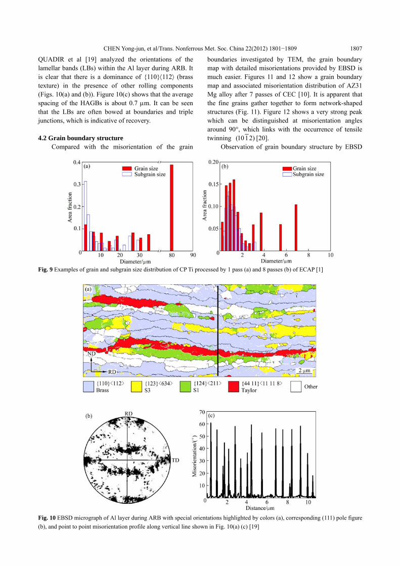
where He is the electron image width, μm; C is constant depending on the EBSD hardware. In our set up, C is 80246 μm. Figure 7 shows that the optimum step size decreases sharply at low magnification and decreases slightly at high magnification. This figure is very useful to find the optimum magnification when a step size is decided. Therefore, it is strongly recommended to have a bigger scan area at high magnification instead of a small area at very low magnification, as schematically shown in Fig. 8.
Fig. 7 Optimum step size as function of magnification [4]
Fig. 8 Schematic showing relationship between scan area and magnification
In general, the minimum grain/subgrain size that can be investigated is dependent on the spatial resolution of the equipment. For a FESEM, the spatial resolution of EBSD tends to get worse slightly as the probe current increases from 10 nA to 100 nA [4,18]. The chosen step size should not be smaller than the spatial resolution. Therefore, a real minimum grain/subgrain size that can be investigated for each EBSD scan is based on the chosen step size. At least 5 pixels per grain/subgrain are required to obtain an accuracy of 10% and a minimum of ~8 pixels per grain/subgrain are required to have an accuracy of 5% [18]. 4 Analysis by EBSD 4.1 Grain/subgrains and texture
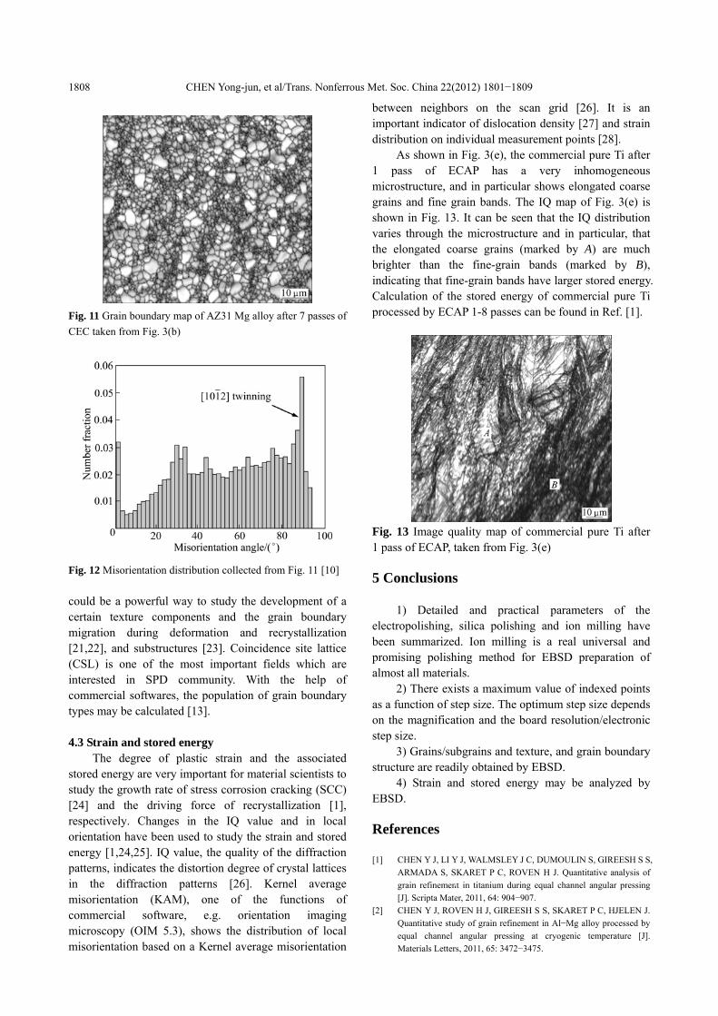
A lot of quantitative information can be obtained from one EBSD scan. Taking the orientation maps of Figs. 3(e) and (f) for example, the same color means similar orientation. Low angle grain boundaries (LAGBs), with misorientations of 1.5°−15° and high angle grain boundaries (HAGBs), with misorientations above 15°, are marked with thin blue lines and thick black lines, respectively. It is apparent that Fig. 3(e) shows a mixture of elongated coarse grains, twins (examples are marked by A and B) and fine-grain bands. In Fig. 3(f), the grains are slightly elongated and aligned at about 11° to the extrusion axis. The grain and subgrain size distributions (equivalent circle diameter) can be easily obtained from the orientation maps, as shown in Fig. 9 [1]. Figure 9 shows the evolution of grain size with increasing strain of SPD and the mean subgrain and grain sizes of these distributions. Details can be found in Ref. [1].
In addition to quantitative study, the orientation map can also be used for detailed investigation on texture, special orientations and point to point misorientation.
CHEN Yong-jun, et al/Trans. Nonferrous Met. Soc. China 22(2012) 1801−1809
1807
QUADIR et al [19] analyzed the orientations of the lamellar bands (LBs) within the Al layer during ARB. It is clear that there is a dominance of {110}⟨112⟩ (brass texture) in the presence of other rolling components (Figs. 10(a) and (b)). Figure 10(c) shows that the average spacing of the HAGBs is about 0.7 μm. It can be seen that the LBs are often bowed at boundaries and triple junctions, which is indicative of recovery. 4.2 Grain boundary structure
Compared with the misorientation of the grain
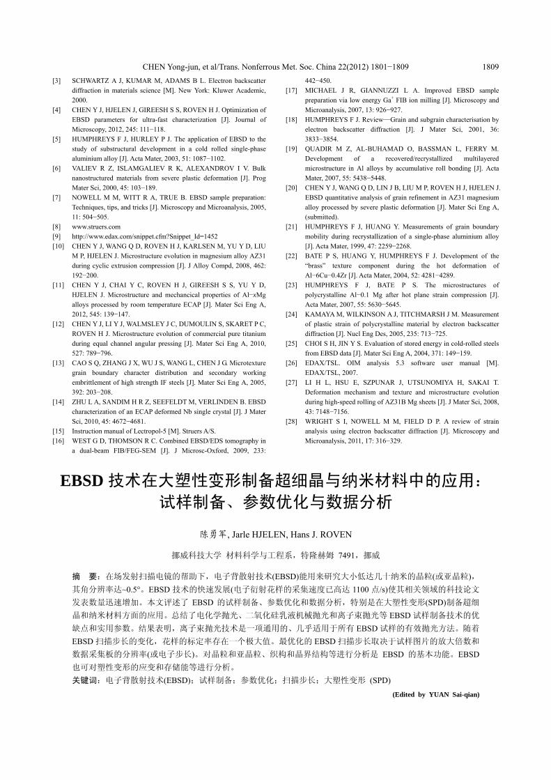
boundaries investigated by TEM, the grain boundary map with detailed misorientations provided by EBSD is much easier. Figures 11 and 12 show a grain boundary map and associated misorientation distribution of AZ31 Mg alloy after 7 passes of CEC [10]. It is apparent that the fine grains gather together to form network-shaped structures (Fig. 11). Figure 12 shows a very strong peak which can be distinguished at misorientation angles around 90°, which links with the occurrence of tensile twinning )2110( [20].
Observation of grain boundary structure by EBSD
Fig. 9 Examples of grain and subgrain size distribution of CP Ti processed by 1 pass (a) and 8 passes (b) of ECAP [1]
Fig. 10 EBSD micrograph of Al layer during ARB with special orientations highlighted by colors (a), corresponding (111) pole figure (b), and point to point misorientation profile along vertical line shown in Fig. 10(a) (c) [19]
CHEN Yong-jun, et al/Trans. Nonferrous Met. Soc. China 22(2012) 1801−1809
1808
Fig. 11 Grain boundary map of AZ31 Mg alloy after 7 passes of CEC taken from Fig. 3(b)
Fig. 12 Misorientation distribution collected from Fig. 11 [10]
could be a powerful way to study the development of a certain texture components and the grain boundary migration during deformation and recrystallization [21,22], and substructures [23]. Coincidence site lattice (CSL) is one of the most important fields which are interested in SPD community. With the help of commercial softwares, the population of grain boundary types may be calculated [13]. 4.3 Strain and stored energy
The degree of plastic strain and the associated stored energy are very important for material scientists to study the growth rate of stress corrosion cracking (SCC) [24] and the driving force of recrystallization [1], respectively. Changes in the IQ value and in local orientation have been used to study the strain and stored energy [1,24,25]. IQ value, the quality of the diffraction patterns, indicates the distortion degree of crystal lattices in the diffraction patterns [26]. Kernel average misorientation (KAM), one of the functions of commercial software, e.g. orientation imaging microscopy (OIM 5.3), shows the distribution of local misorientation based on a Kernel average misorientation
between neighbors on the scan grid [26]. It is an important indicator of dislocation density [27] and strain distribution on individual measurement points [28].
As shown in Fig. 3(e), the commercial pure Ti after 1 pass of ECAP has a very inhomogeneous microstructure, and in particular shows elongated coarse grains and fine grain bands. The IQ map of Fig. 3(e) is shown in Fig. 13. It can be seen that the IQ distribution varies through the microstructure and in particular, that the elongated coarse grains (marked by A) are much brighter than the fine-grain bands (marked by B), indicating that fine-grain bands have larger stored energy. Calculation of the stored energy of commercial pure Ti processed by ECAP 1-8 passes can be found in Ref. [1].
Fig. 13 Image quality map of commercial pure Ti after 1 pass of ECAP, taken from Fig. 3(e) 5 Conclusions
1) Detailed and practical parameters of the electropolishing, silica polishing and ion milling have been summarized. Ion milling is a real universal and promising polishing method for EBSD preparation of almost all materials.
2) There exists a maximum value of indexed points as a function of step size. The optimum step size depends on the magnification and the board resolution/electronic step size.
3) Grains/subgrains and texture, and grain boundary structure are readily obtained by EBSD.
4) Strain and stored energy may be analyzed by EBSD. References [1] CHEN Y J, LI Y J, WALMSLEY J C, DUMOULIN S, GIREESH S S,
ARMADA S, SKARET P C, ROVEN H J. Quantitative analysis of grain refinement in titanium during equal channel angular pressing [J]. Scripta Mater, 2011, 64: 904−907.
[2] CHEN Y J, ROVEN H J, GIREESH S S, SKARET P C, HJELEN J. Quantitative study of grain refinement in Al−Mg alloy processed by equal channel angular pressing at cryogenic temperature [J]. Materials Letters, 2011, 65: 3472−3475.
A
CHEN Yong-jun, et al/Trans. Nonferrous Met. Soc. China 22(2012) 1801−1809
1809[3] SCHWARTZ A J, KUMAR M, ADAMS B L. Electron backscatter
diffraction in materials science [M]. New York: Kluwer Academic, 2000.
[4] CHEN Y J, HJELEN J, GIREESH S S, ROVEN H J. Optimization of EBSD parameters for ultra-fast characterization [J]. Journal of Microscopy, 2012, 245: 111−118.
[5] HUMPHREYS F J, HURLEY P J. The application of EBSD to the study of substructural development in a cold rolled single-phase aluminium alloy [J]. Acta Mater, 2003, 51: 1087−1102.
[6] VALIEV R Z, ISLAMGALIEV R K, ALEXANDROV I V. Bulk nanostructured materials from severe plastic deformation [J]. Prog Mater Sci, 2000, 45: 103−189.
[7] NOWELL M M, WITT R A, TRUE B. EBSD sample preparation: Techniques, tips, and tricks [J]. Microscopy and Microanalysis, 2005, 11: 504−505.
[8] www.struers.com [9] http://www.edax.com/snippet.cfm?Snippet_Id=1452 [10] CHEN Y J, WANG Q D, ROVEN H J, KARLSEN M, YU Y D, LIU
M P, HJELEN J. Microstructure evolution in magnesium alloy AZ31 during cyclic extrusion compression [J]. J Alloy Compd, 2008, 462: 192−200.
[11] CHEN Y J, CHAI Y C, ROVEN H J, GIREESH S S, YU Y D, HJELEN J. Microstructure and mechancical properties of Al−xMg alloys processed by room temperature ECAP [J]. Mater Sci Eng A, 2012, 545: 139−147.
[12] CHEN Y J, LI Y J, WALMSLEY J C, DUMOULIN S, SKARET P C, ROVEN H J. Microstructure evolution of commercial pure titanium during equal channel angular pressing [J]. Mater Sci Eng A, 2010, 527: 789−796.
[13] CAO S Q, ZHANG J X, WU J S, WANG L, CHEN J G. Microtexture grain boundary character distribution and secondary working embrittlement of high strength IF steels [J]. Mater Sci Eng A, 2005, 392: 203−208.
[14] ZHU L A, SANDIM H R Z, SEEFELDT M, VERLINDEN B. EBSD characterization of an ECAP deformed Nb single crystal [J]. J Mater Sci, 2010, 45: 4672−4681.
[15] Instruction manual of Lectropol-5 [M]. Struers A/S. [16] WEST G D, THOMSON R C. Combined EBSD/EDS tomography in
a dual-beam FIB/FEG-SEM [J]. J Microsc-Oxford, 2009, 233:
442−450. [17] MICHAEL J R, GIANNUZZI L A. Improved EBSD sample
preparation via low energy Ga+ FIB ion milling [J]. Microscopy and Microanalysis, 2007, 13: 926−927.
[18] HUMPHREYS F J. Review—Grain and subgrain characterisation by electron backscatter diffraction [J]. J Mater Sci, 2001, 36: 3833−3854.
[19] QUADIR M Z, AL-BUHAMAD O, BASSMAN L, FERRY M. Development of a recovered/recrystallized multilayered microstructure in Al alloys by accumulative roll bonding [J]. Acta Mater, 2007, 55: 5438−5448.
[20] CHEN Y J, WANG Q D, LIN J B, LIU M P, ROVEN H J, HJELEN J. EBSD quantitative analysis of grain refinement in AZ31 magnesium alloy processed by severe plastic deformation [J]. Mater Sci Eng A, (submitted).
[21] HUMPHREYS F J, HUANG Y. Measurements of grain boundary mobility during recrystallization of a single-phase aluminium alloy [J]. Acta Mater, 1999, 47: 2259−2268.
[22] BATE P S, HUANG Y, HUMPHREYS F J. Development of the “brass” texture component during the hot deformation of Al−6Cu−0.4Zr [J]. Acta Mater, 2004, 52: 4281−4289.
[23] HUMPHREYS F J, BATE P S. The microstructures of polycrystalline Al−0.1 Mg after hot plane strain compression [J]. Acta Mater, 2007, 55: 5630−5645.
[24] KAMAYA M, WILKINSON A J, TITCHMARSH J M. Measurement of plastic strain of polycrystalline material by electron backscatter diffraction [J]. Nucl Eng Des, 2005, 235: 713−725.
[25] CHOI S H, JIN Y S. Evaluation of stored energy in cold-rolled steels from EBSD data [J]. Mater Sci Eng A, 2004, 371: 149−159.
[26] EDAX/TSL. OIM analysis 5.3 software user manual [M]. EDAX/TSL, 2007.
[27] LI H L, HSU E, SZPUNAR J, UTSUNOMIYA H, SAKAI T. Deformation mechanism and texture and microstructure evolution during high-speed rolling of AZ31B Mg sheets [J]. J Mater Sci, 2008, 43: 7148−7156.
[28] WRIGHT S I, NOWELL M M, FIELD D P. A review of strain analysis using electron backscatter diffraction [J]. Microscopy and Microanalysis, 2011, 17: 316−329.
EBSD 技术在大塑性变形制备超细晶与纳米材料中的应用: 试样制备、参数优化与数据分析
陈勇军, Jarle HJELEN, Hans J. ROVEN
挪威科技大学 材料科学与工程系,特隆赫姆 7491,挪威
摘 要:在场发射扫描电镜的帮助下,电子背散射技术(EBSD)能用来研究大小低达几十纳米的晶粒(或亚晶粒),其角分辨率达~0.5°。EBSD 技术的快速发展(电子衍射花样的采集速度已高达 1100 点/s)使其相关领域的科技论文
发表数量迅速增加。本文评述了 EBSD 的试样制备、参数优化和数据分析,特别是在大塑性变形(SPD)制备超细
晶和纳米材料方面的应用。总结了电化学抛光、二氧化硅乳液机械抛光和离子束抛光等 EBSD 试样制备技术的优
缺点和实用参数。结果表明,离子束抛光技术是一项通用的、几乎适用于所有 EBSD 试样的有效抛光方法。随着
EBSD 扫描步长的变化,花样的标定率存在一个极大值。最优化的 EBSD 扫描步长取决于试样图片的放大倍数和
数据采集板的分辨率(或电子步长)。对晶粒和亚晶粒、织构和晶界结构等进行分析是 EBSD 的基本功能。EBSD也可对塑性变形的应变和存储能等进行分析。 关键词:电子背散射技术(EBSD);试样制备;参数优化;扫描步长;大塑性变形 (SPD)
(Edited by YUAN Sai-qian)


![Investigation of electropolishing characteristics of tungsten in ......of electropolishing tungsten has been studied by Wang et al. [21], and they discovered that electropolishing](https://img.dokumen.tips/doc/110x75/60eb316d7c2235457f18455e/investigation-of-electropolishing-characteristics-of-tungsten-in-of-electropolishing.jpg)