Embed Size (px)
Citation preview

Application Notes: SY6982E High Efficiency, 2A, Two-Cell Boost Li-Ion Battery Charger
General Description SY6982E is a 3.6-5.5VIN, 2A two-cell synchronous boost Li-Ion battery charger integrates 1MHz switching frequency and full protection functions. The charge current up to 2A can be programmed by using the external resistor for different portable applications and indicates the charger current information simultaneous. It also has a programmable charge timeout for safety battery charge operation and a programmable input voltage threshold for adaptive input current limit. SY6982E can disconnect output when there is output short circuit or shutdown happens. It consists of 18V rating FETs with extremely low ON resistance to achieve high charge efficiency and simple peripheral circuit design. SY6982E along with small QFN3x3 footprint provides small PCB area application. Ordering Information SY6982 ()
Temperature Code Package Code Optional Spec Code
Ordering Number Package type Note SY6982EQDC QFN3x3-16
Features Low Profile QFN3x3 Package
Integrated Synchronous Boost with 18V Rating Low RDSON FETs for High Charge Efficiency Trickle Current / Constant Current / Constant Voltage Charge Mode Programmable Input Voltage Threshold for Adaptive Current Limit. Maximum 2A Constant Charge Curre t Charge Current Information Indication. Programmable Charge Timeout Programmable Constant Charge Current Selectable Constant Voltage ±0.5% Battery Voltage Accuracy Thermal Regulation Pr tection External Shutdown Function Input Voltage UVLO and OVP Over Temp rature Protection Output Sho t Circuit Protection Charge St tus Indication Normal Synchronous Boost Operation When Battery Removed
Applications Cellular Telephones, PDA, MP3 Players, MP4 Players
Digital Cameras Bluetooth Applications
PSP Game Players, NDS Game Players Notebook
Typical Applications
Figure1. Schematic Diagram AN_SY6982E_Rev.0.9D Silergy Corp. Confidential- Prepared for Customer Use Only 1

AN_SY6982E
Pinout (top view)
(QFN3x3-16) Top Mark: AWFxyz, (Device code: AWF, x=year code, y=week code, z= l t number code)
Name Pin Number Description
STAT 1 Charge status indication pin. It is open drain output pin and pull high to SVIN thru a LEDto indicate the charge in process. When the cha ge is done, LED is off.
System ON/OFF control pin. When VBAT is lower than 6V, SYSRT pin outputs low logicSYSRT 2 to turn off the system operation; when VBAT is high than 6V, SYSRT pin outputs high
logic to turn on the system operation. Charge time limit pin. Connect this pin with a capacitor to ground. Internal current source
TIM 3 charge the capacitor for TC mode and CC mode’s charge time limit. TC charge time limit is about 1/9 of CC charge time. Thermal protection pin. UTP hreshold is typical 75%VSVIN and OTP threshold is typical
NTC 4 30%VSVIN. Pull up to SVIN can disable charge logic and make the IC operate as normal boost regulator. Pull down to ground can shutdown the IC.
CV 5 Battery CV voltage selection pin. Program 2 different CV thresholds by setting different voltage on the pin. The detailed information is shown in description section.
VSEN 6 Voltage sense of SVIN. If the voltage drops to internal 1.195V reference voltage, the SVIN will be clamped to setting value and input current will be limited.
EN 7 Enable control pin. High logic for enable on, and low logic for enable off. SGND 8 Signal ground pin.
Charge current program pin, pull down to GND with a Resistor RICHG. The mirror current
ICHG 9 about 1/10000 of the blocking FET current will dump into the external RC network thruICHG pin and compared to the internal reverence 1V. So ICC=(1V/ RICHG)x10000,
ITC=(1V/ RICHG)x1000. BD 10, 13 Connect to the Drain of internal Blocking FET. Bypass at least 4.7uF ceramic cap to
GND.
BST 11 Boost-Strap pin. Supply Rectified FET’s gate driver. Decouple this pin to LX with 0.1uF ceramic cap.
BAT 12 Battery positive pin. LX 14 Switch node pin. Connect to external inductor.
PGND 15 Power ground pin. Analog power input pin. Connect a MLCC from this pin to ground to decouple high
SVIN 16 harmonic noise. This pin has OVP and UVLO function to make the charger operate within safe input voltage area. AN_SY6982E_Rev.0.9D Silergy Corp. Confidential- Prepared for Customer Use Only 2

AN_SY6982E
Absolute Maximum Ratings STAT, NTC, CV, VSEN, EN, ICHG, BD, BAT, LX, SVIN -------------------------------------------------------------- 18VSYSRT, TIM, BST-LX ----------------------------------------------------------------------------------------------------------- 4VLX Pin current continuous ----------------------------------------------------------------------------------------------------- 5APower Dissipation, PD @ TA = 25°C, QFN3X3 ---------------------------------------------------------------------------- 2.6WPackage Thermal Resistance
θJA --------------------------------------------------------------------------------------------------------------------- 38°C/WθJC ----------------------------------------------------------------------------------------------------------------------- 4°C/W
Junction Temperature Range -------------------------------------------------------------------------------- -40°C to +125°CLead Temperature (Soldering, 10 sec.) --------------------------------------------------------------------------------- 260°CStorage Temperature Range ---------------------------------------------------------------------------------- -65°C to 125°C
Recommended Operating Conditions SVIN -------------------------------------------------------------------------------------------------------------------- 3.6V to 5.5V STAT, NTC, CV, VSEN, EN, ICHG, BD, BAT, LX, --------------------------------------------------------- -0.3V to 16VSYSRT, TIM -------------------------------------------------------------------------------------------------------- -0.3V to 3.3VLX Pin current continuous ----------------------------------------------------------------------------------------------------- 5AJunction Temperature Range ------------------------------------------------------------------------------------ -40°C to 125°CAmbient Temperature Range ------------------------------------------------------------------------------------ -40°C to 85°C
AN_SY6982E_Rev.0.9D Silergy Corp. Confidential- Prepared for Customer Use Only 3

AN_SY6982E Electrical Characteristics TA=25°C, VIN=5V, GND=0V, CIN=4.7uF, L=0.68uH, RICHG=10kΩ, CTIM=470nF, unless otherwise specified. Symbol Parameter Conditions Min Typ Max Unit
Bias Supply (VSVIN) V
SVIN Supply voltage 3.6 16 VV
UVLO
VSVIN under voltage lockout VSVIN rising and measured
3.6 V threshold from VSVIN to GND ∆V
UVLO VSVIN under voltage lockout Measured from VSVIN to GND 100 mV hysteresis
VOVP Input overvoltage protection
VSVIN rising and measured5.8
V from VSVIN to GND
∆VOVP Input overvoltage protection Measured from VSVIN to GND 0.5 V
hysteresis
Quiescent Current I
BAT Battery discharge current Shutdown IC, EN=NTC=0 10 uAI
IN Input quiescent current Disable Charge,
1.5 mA EN=1,NTC=0
Oscillator and PWM fSW Switching frequency 1000 kHz
TMINOFF Main N-FET minimum off time With 18V rating 100 ns
TMAXOFF Main N-FET maximum off time With 18V rating 30 us
TMINON Main N-FET minimum on time With 18V rating 100 ns
Power MOSFET R
NFET_M RDS(ON) of Main N-FET 80 mΩR
NFET_R RDS(ON) of Rectified N-FET 40 mΩR
NFET_B RDS(ON) of Blocking N-FET 40 mΩVoltage Regulation
VCV<1V 8.358 8.40 8.442 V
CV 2-Cell CV charge mode voltage
VVCV>2V 8.656 8.70 8.743
VCVH High level logic for CV1/2 2 V
VCVL Low level logic for CV1/2 1 V
∆VRCH 2-Cell Recharge Voltage 100 200 300 mV
VTRK 2-cell TC charge mode battery Rising edge threshold 5.4 5.6 5.8 V
voltage threshold
Battery Connect Detection V
DET NTC voltage threshold for Battery
85%
95%V
SVINdetect NTC Falling Edge t
DET Detect delay time 30 msCharge Current
Internal charge current accuracy for ICC=1000mA -10% 10% Constant Current Mode
Internal charge current accuracy for ITC=100mA -50% 50% Trickle Current Mode
ITERM Termination current ICC=1000mA 50 100 150 mA
Output Voltage OVP V
OVP Output voltage OVP threshold 105% 110% 115% VCV
Input Voltage Threshold for Adaptive Current Limit V
Threshold Voltage reference of VSEN 1.171 1.195 1.219 VTimer
AN_SY6982E_Rev.0.9D Silergy Corp. Confidential- Prepared for Customer Use Only 4

AN_SY6982E
TTC Trickle current charge timeout CTIM=330nF 0.23 0.5 0.67 hour
TCC Constant current charge timeout 3.0 4.5 6 hour TMC Charge mode change delay time 30 ms
TTERM Termination delay time 30 ms
TRCHG Recharge time delay 30 ms
Short Circuit Protection V
SHORT Output short protection threshold 1.70 2.00 2.30 VSystem ON/OFF Control V
HSYSRT High logic of system ON/OFF
2.1
V control
VLSYSRT
Low logic of system ON/OFF 0.6 V control
VHYSSYS
Hysteresis for positive and negative 100
mVedge
Linear charger Mode ILCHG Battery Charger current when the
VBAT
<VSHORT 5%
ICC
blocking FET is in linear mode
ILPEAK
Peak linear current when Battery is 1
A absent
VBD Bus voltage regulation 5.8 6 6.2 VVTRON Blocking FET fully turn on
VBAT
> VTRK 100 mV
threshold VTRON=VBAT-VIN
Enable ON/OFF Control V
ENH High level logic for enable control 1.5 VV
ENL Low level logic for enable control 0.4 VBattery Thermal Protection NTC
Under temperature protection 70% 75% 80%
UTP Under temperature protection Fall ng edge 5% hysteresis V
SVIN Over temperature protection 28% 30% 32%OTP Over temperature protection Rising edge 2%
hysteresis Thermal Regulation And Thermal shutdown T
REG Thermal regulation threshold Rising Threshold 120 ºCT
REGHYS Thermal regulation hysteresis
20
ºC falling edge
Thermal regulation fold back ratio 0.25 ICC
TSD Thermal shutdown temperature Rising Threshold 160 ºC
TSDHYS
Thermal shutdown temperature 30
ºC hysteresis
Note 1: Stresses be ond the “Absolute Maximum Ratings” may cause permanent damage to the device. These are stress ratings only. Functional operation of the device at these or any other conditions beyond those indicated in the operational s ctions of the specification is not implied. Exposure to absolute maximum rating conditions for extended periods may affect device reliability.
Note 2: θ JA is measured in the natural convection at TA = 25°C on a low effective four-layer thermal conductivity test board of JEDEC 51-3 thermal measurement standard.
Note 3: The device is not guaranteed to function outside its operating conditions
AN_SY6982E_Rev.0.9D Silergy Corp. Confidential- Prepared for Customer Use Only 5

AN_SY6982E General Function Description SY6982E is a 3.6-5.5VIN, 2A two-cell synchronous boost Li-Ion battery charger integrates 1MHz switching frequency and full protection functions. The charge current up to 2A can be programmed by using the external resistor for different portable applications and indicates the charger current information simultaneous. It also has a programmable charge timeout for safety battery charge operation and a programmable input voltage threshold for adaptive input current limit. SY6982E can disconnect output when there is output short circuit or shutdown happens. It consists of 18V rating FETs with extremely low ON resistance to achieve high charge efficiency and simple peripheral circuit design. Charging Status Indication Description 1. Charge-In-Process – Pull and keep STAT pin to
Low; 2. Charge Done – Pull and keep STAT pin to High; 3. Fault Mode – Output high and low voltage
alternatively with 1.3Hz frequency. Connect a LED from SVIN to STAT pin, LED ON means Charge-in-Process, LED OFF means Charge Done, LED Flashing with 1.3HZ means Fault Mode.
Switching Mode Boost Charger Basic Operation Description Switching Mode Control Strategy SY6982E is a switching mode Boost charger for the applications with USB power input. The 1MHz fixed frequency is easy for the size minimization of peripheral circuit design. Operation Principle SY6982E can normally work with or without Li-Ion battery both.
Battery Present When the battery is present, SY6982E will works on trickle charging, constant current charging and constant voltage charging mode according to the battery voltage. Battery Absent If there’s no battery connection detected thru NTC pin, SY6982E operates as a normal switching mode boost converter. The internal constant current loop and voltage loop are active both. Basic Protection Principle SY6982E has fully battery charging protect on. When the input over voltage protection, the output over voltage protection, the thermal protection or the timeout protection happens, the b st charger stops switching immediately. When the VBAT is lower than VSHORT, the short circuit p otection happens. The main FET is turned off firstly. The block FET enters linear mode with 1/20 ICC charging current. When VBAT recovers back to be higher than VSHORT, the boost charger restarts to work at light load and regulates VBD at 6V. The line charge current is increased from 1/20 ICC to 1/10 ICC. When VBAT recovers back to be higher than VSVIN, the boost switching charger takes over. Adaptive Input Current Limit Principle SY6982E can protect the input DC source from over load by the special loop control. The high charging current will caused a voltage drop at SVIN when the input DC source is over load. When VSEN drops below the internal 1.195V reference, SY6982E will decrease the duty cycle to reduce the charging current. Constant Voltage Threshold Program Principle SY6982E can program the constant voltage threshold thru the CV pin. When VCV is higher than 2V, the constant voltage threshold is 8.7V; when VCV is lower than 1V, the constant voltage threshold is 8.4V.
AN_SY6982E_Rev.0.9D Silergy Corp. Confidential- Prepared for Customer Use Only 6

AN_SY6982E
Typical Performance Characteristics (TA=25°C, VIN=5V, RRCH=10kΩ, unless otherwise specified. )
Efficiency vs. Bat voltage (CC mode) 97.5
97.0
(%)
96.5Efficiency 96.0
95.5
95.0
94.5
6.0 6.4 6.8 7.2 7.6 8.0 8.4
Bat Voltage (V)
Steady waveform (CC Mode)
BAT 2V/div
IL 1A/div
LX 5V/div
Time (2µs/div)
Steady waveform (TC Mode)
BAT 5V/div
BD 5V/div
IL 2A/div
LX 5V/div
Time (10µs/div)
Efficiency vs. Charge current (CV mode)
98.0
97.0(%)
96.0Efficiency 94.0 95.0
93.0
92.0
0 0.2 0.4 0.6 0.8 1 Charge Current (A)
St ady waveform (CV Mode)
BAT 5V/div
IL 2A/div
LX 5V/div
Time (2µs/div)
Steady waveform (Short Mode)
BAT 5V/div
STAT 5V/div
IL 50mA/div
LX 5V/div
Time (1s/div) AN_SY6982E_Rev.0.9D Silergy Corp. Confidential- Prepared for Customer Use Only 7

AN_SY6982E
Power On (CC Mode)
STAT 5V/div BAT 5V/div IL 2A/div
LX 5V/div
Time (400ms/div)
Power On (CV Mode) STAT 5V/div BAT 5V/div IL 5A/div LX 5V/div
Time (400ms/div)
Adaptive input current limit
(5V/1A adapter) VIN 2V/div
IO 0.5A/div
Power Off (CC Mode)
STAT 5V/div
BAT 5V/div
IL 2A/div
LX 5V/div
Time (2ms/div)
Boost Mode (Null load) STAT 2V/div BAT 5V/div
IIN 1A/div IL 1A/div
LX 5V/div LX 5V/div
Time (1µs/div) Time (20µs/div)
AN_SY6982E_Rev.0.9D Silergy Corp. Confidential- Prepared for Customer Use Only 8

AN_SY6982E
Applications Information Because of the high integration of SY6982E, the application circuit based on this regulator IC is rather simple. Only input capacitor CIN, output capacitor COUT, inductor L, NTC resistors R1,R2, input voltage threshold resistors Rup, Rdown and timer capacitor CTIM need to be selected for the targeted applications specifications. NTC resistor: SY6982E monitors battery temperature by measuring the input voltage and NTC voltage. The controller triggers the UTP or OTP when the rate K (K= VNTC/VSVIN) reaches the threshold of UTP (KUT) or OTP (KOT). The temperature sensing network is showed as below. Choose R1 and R2 to program the proper UTP and OTP points.
The input voltage sense network shows below, choose Rup,Rdown to set the input voltage threshold V
INT :
VINT = VSEN*(Rdown + Rup) Unit:V
Rdown
VSEN is 1.195V. Timer capacitor CTIM The charger also provides a programmable charge timer. The charge time is programmed by the capacitor connected between the TIM pin and GND. The ca acitance is given by the formula: CTIM=2*10-11TCC Unit:F TCC is the target constant charge time,unit: s. Input capacitor CIN:
The calculation steps are: 1. Define KUT, KUT =70~80% 2. Define KOT, KOT =28~32% 3. Assume the resistance of the battery NTC
thermistor is RUT at UTP threshold a d ROT at OTP threshold.
4. Calculate R2,
R2 = KOT (1− KUT )RUT − K UT (1− KOT)ROT
KUT - KOT
5. Calculate R1
R1 = (1/ KOT − 1)(R2 + ROT ) If choose the typical values KUT =75% and KOT=30%, then
R2 = 0.17RUT −1.17ROT R1 = 2.3(R2 + ROT )
Input Voltage Threshold VSEN for Adaptive Current Limit. SY6982E monitors input voltage by measuring the VSEN voltage, when VSEN drops below the internal 1.195V reference, SY6982E will decrease the duty cycle to reduce the charging current.
The ripple current through input capacitor is greater than
= V IN *(VOUT − V IN) ICIN_RMS
2 3 * L*FSW * VOUT X5R or X7R ceramic capacitors with greater than 4.7uF capacitance are recommended to handle this ripple current. Output capacitor COUT : The output capacitor is selected to handle the output ripple noise requirements. This ripple voltage is related to the capacitance and its equivalent series resistance (ESR). For the best performance, it is recommended to use X5R or better grade low ESR ceramic capacitor. The voltage rating of the output capacitor should be higher than the maximum output voltage. The minimum required capacitance can be calculated as:
= ICC*(VOUT − VIN) COUT
FSW × VOUT × VRIPPLE VRIPPLE is the peak to peak output ripple, ICC is the setting charge current. For SY6982E, output capacitor is paralleled by CBD and CBAT, for smaller output ripple noise, each
AN_SY6982E_Rev.0.9D Silergy Corp. Confidential- Prepared for Customer Use Only 9

AN_SY6982E capacitor with greater than 10uF capacitance is recommended. Inductor L: There are several considerations in choosing this inductor. 1) Choose the inductance to provide the desired
ripple current. It is suggested to choose the ripple current to be about 40% of the average input current. The inductance is calculated as:
DCR<10mohm to achieve a good overall efficiency.
Layout Design: The layout design of SY6982E regulator is relatively simple. For the best efficiency and minimum noise problems, we should place the following components close to the IC: CSVIN, L, CBD. 1) The loop of main MOSFET, rectifier diode, and
CBD must be as short as possible VIN 2 (VOUT − VIN)
L =
ICC × FSW × 40% VOUT
Where FSW is the switching frequency and ICC is the setting charge current. The SY6982E is quite tolerant of different ripple current amplitude. Consequently, the final choice of inductance can be slightly off the calculation value without significantly impacting the performance.
2) The saturation current rating of the inductor must be selected to be greater than the peak inductor current under full load conditions. VOUT VIN (VOUT − VIN)
ISAT,MIN > × ICC +
×
× FSW × L VIN VOUT 2 3) The DCR of the inductor and the core loss at the
switching frequency must be low enough to achieve the desired efficiency requirement. It is desirable to choose an inductor with
2) It is desirable to maximize the PCB copper area
connecting to GND pin to achieve the best thermal and noise performance.
3) CSVIN must be close to pin SVIN and GND. 4) The PCB copper area associated with LX pin must be minimized to avoid the potential noise probl m. 5) The small signal components RICHG ,Rup and Rdown must be placed close to IC and must not be adjacent to the LX net on the PCB layout to avoid the noise problem.
AN_SY6982E_Rev.0.9D Silergy Corp. Confidential- Prepared for Customer Use Only 10
AN_SY6982E
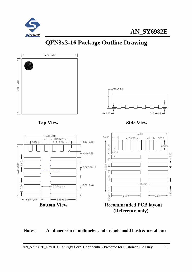
QFN3x3-16 Package Outline Drawing
Top View Side View
Bottom View Recommended PCB layout (Reference only)
Notes: All dimension in millimeter and exclude mold flash & metal burr
AN_SY6982E_Rev.0.9D Silergy Corp. Confidential- Prepared for Customer Use Only 11

AN_SY6982E
Taping & Reel Specification 1. Taping orientation
QFN3x3
Feeding direction 2. Carrier Tape & Reel specification for packages
Reel Size
Package type Tape width Pocket Reel size Trailer Leader length Qty per (mm) pitch(mm) (Inch) length(mm) (mm) reel
QFN3x3 12 8 13" 400 400 5000
3. Others: NA
AN_SY6982E_Rev.0.9D Silergy Corp. Confidential- Prepared for Customer Use Only 12