Embed Size (px)
Citation preview
Testing FPGA-Based Hardware Emulators with Slow I/Q Signals Application Note
Products:
| R&SSMU200A
| R&SAMU200A
| R&SSMBV100A
| R&SSMJ100A
| R&SEX-IQ-BOX
During the design process of chipsets or
modules, FPGA-based hardware
emulators are utilized to perform early
tests with real test and measurement
instruments. These hardware emulators
usually run at artificially reduced speed,
but apart from that function like the
finished design.
In this application note we explain how to
test FPGA-based hardware emulators
using Rohde & Schwarz vector signal
generators for creating suitable real-time
test signals at reduced sample rates. We
further explain how to correctly adapt
AWGN signal generation and fading
simulation for “slow I/Q”.
App
licat
ion
Not
e
C. T
röst
er-S
chm
id
11.2
012-
1GP
95_0
E

Table of Contents
1GP95_0E Rohde & Schwarz Testing FPGA-Based Hardware Emulators with Slow I/Q Signals 2
Table of Contents
1 Introductory Note ................................................................... 3
2 Introduction ............................................................................ 3
3 Background ............................................................................ 5
4 Test Setup ............................................................................... 8
5 Signal Generator Settings ..................................................... 9
5.1 Baseband Signal .......................................................................................... 9
5.2 AWGN Signal ................................................................................................ 9
5.3 Fading Simulation ......................................................................................11
5.3.1 Adjusting Path Delays ...............................................................................11
5.3.2 Adjusting Doppler Shifts ...........................................................................13
5.4 Digital I/Q Output Settings .........................................................................15
5.5 HARQ Feedback .........................................................................................15
6 Abbreviations ....................................................................... 16
7 References ............................................................................ 16
8 Ordering Information ........................................................... 16

Introductory Note
1GP95_0E Rohde & Schwarz Testing FPGA-Based Hardware Emulators with Slow I/Q Signals 3
1 Introductory Note The following abbreviations are used in this application note for Rohde & Schwarz
products:
The R&S®SMU200A vector signal generator is referred to as SMU.
The R&S®SMBV100A vector signal generator is referred to as SMBV.
The R&S®SMJ100A vector signal generator is referred to as SMJ.
The R&S®AMU200A baseband signal generator and fading simulator is
referred to as AMU.
The R&S®EX-IQ-BOX digital interface module is referred to as EX-IQ-BOX.
2 Introduction Modern mobile radio standards such as LTE or LTE-Advanced are significantly more
complex than 2nd generation standards such as GSM. Not only are the physical
transmission methods different – OFDM and MIMO instead of single-carrier GMSK
modulation, for example – the entire preprocessing stage for user data is much more
demanding. This is a particular challenge in the development of RF and baseband
modules. Accordingly, more emphasis is placed today on design verification at the
various stages of the process.
For example, any 3GPP FDD/LTE chipset or module design starts with a complete
specification of the required attributes. Based on this specification, the design is
modeled using algorithm design and simulation tools. During software simulation, the
design of the chip is verified against the 3GPP FDD/LTE standard. This is done using
stimuli and channel models, and using software models of ideal reference receivers.
Then the design is split into the software and hardware components that need to be
developed, and the hardware and software is co-simulated. If the simulation is
satisfactory, development typically continues with FPGA-based hardware emulators.
These usually run at an artificially reduced speed, but apart from that function just like
the finished design. This makes it possible to perform initial tests using real test and
measurement instruments relatively early in the design process. Iterative verification
using software simulation and real test and measurement instruments leads to the first
prototype of a chipset or module. The chipset or module is again verified with test and
measurement instruments before it is integrated into a more complex design such as a
mobile phone or a base station.

Introduction
1GP95_0E Rohde & Schwarz Testing FPGA-Based Hardware Emulators with Slow I/Q Signals 4
In this application note we focus on testing FPGA-based hardware emulators which run
at reduced speed. We explain how to configure Rohde & Schwarz vector signal
generators for creating suitable real-time test signals at reduced sample rates and how
to correctly adapt AWGN signal generation and fading simulation.

Background
1GP95_0E Rohde & Schwarz Testing FPGA-Based Hardware Emulators with Slow I/Q Signals 5
3 Background Rohde & Schwarz vector signal generators offer ARB-based as well as real-time signal
generation. When testing hardware emulators using the internal ARB generator, the
playback of waveforms (which are generated/recorded at original speed or obtained
from simulation) can be slowed-down easily. When testing is carried out using the
internal real-time baseband generator, the data generation can be slowed-down as
easily by reducing the sample rate. In both cases, if fading simulation and/or AWGN is
applied to the baseband signal, the situation becomes more advanced. Fading
simulator and AWGN settings need to be adapted to the “slowed-down” state. How to
do this is explained in detail in section 5.
In the following we focus on real-time signal generation and present some fundamental
conditions and related thoughts on a basic level. Advanced users may skip this part
and continue reading in section 4.
In the baseband generator under conventional operating conditions, the data is
generated (continuously) at a certain sample rate, Rsample. Fading simulation and
AWGN can be optionally applied to the signal in the instrument’s digital domain. The
digital data can then be output via the instrument’s digital interface or converted to
analog signals and upconverted to the RF domain. No matter how the data is output
from the signal generator – digitally1, analog or as RF signal – it is output at the sample
rate Rsample as shown in the following figure.
ANALOG
DIGITAL
I/Q OUT
Source
Drain
Rsample
Rsample
A consequence of this fact is that the sample rate needs to be reduced at the
baseband signal source when hardware emulators shall be tested at reduced speed.
This means that also the fading simulator and AWGN settings need to be adapted.
1 Resampling is possible for the digital output, but we disregard resampling at this point for didactic reasons.

Background
1GP95_0E Rohde & Schwarz Testing FPGA-Based Hardware Emulators with Slow I/Q Signals 6
From a hypothetical point of view, let’s assume the data would be generated in the
baseband at Rsample but output at a smaller sample rate R’sample = Rsample /N. On the one
hand, this would avoid having to adjust the fading simulator and AWGN settings, since
both units could keep running at original speed. But on the other hand, this would
generate an unsolvable overflow situation, since the baseband would deliver the data
faster than it could be output. Buffers would be needed to temporary store the data.
However, since a real-time baseband generator supplies data continuously, the
overflow situation would reoccur as the buffer size is always limited. This hypothetical
situation is shown in the following figure.
R’sample = Rsample /N
ANALOG
DIGITAL
I/Q OUT
Source
Drain
Rsample
Again, the consequence is the same as prior to this hypothetical thought: The only
way to achieve a lowered sample rate at the output of the instrument is to reduce the
sample rate at the data source, i.e. the real-time baseband generator needs to be
slowed down.
Finally, we want to mention a potential pitfall. When testing hardware emulators usually
the digital output of the instrument is utilized. Here, the user can set an output sample
rate. The data from the baseband generated at Rsample are resampled to the sample
rate set by the user. What happens if the user sets a lower sample rate R’sample =
Rsample /N? In this case down-sampling takes place, i.e. the number of samples per time
period is reduced. More clearly, samples are dropped as illustrated in the figure below.
This is however not what is needed for testing hardware emulators. The data rate shall
be slowed down keeping all samples; it shall not be reduced by dropping samples.
Down-sampling is thus no suitable method to reduce the sample rate at the digital
output for this particular application.
To emphasize that the sample rate really needs to be slowed down in speed (rather
than being reduced by resampling), we talk about “slow I/Q” signal generation.

Background
1GP95_0E Rohde & Schwarz Testing FPGA-Based Hardware Emulators with Slow I/Q Signals 7
Note that slowing down data generation in the baseband source affects the signal
bandwidth (wanted effect) while resampling leaves the signal bandwidth unchanged.
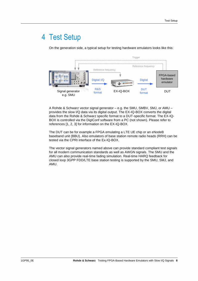
Test Setup
1GP95_0E Rohde & Schwarz Testing FPGA-Based Hardware Emulators with Slow I/Q Signals 8
Signal generator
e.g. SMUDUT
FPGA-based
hardware
emulator
EX-IQ-BOX
Digital I/Q Digital
R&S
formatDUT
format
Reference frequency
Reference frequency
Trigger
4 Test Setup On the generation side, a typical setup for testing hardware emulators looks like this:
A Rohde & Schwarz vector signal generator – e.g. the SMU, SMBV, SMJ, or AMU –
provides the slow I/Q data via its digital output. The EX-IQ-BOX converts the digital
data from the Rohde & Schwarz specific format to a DUT-specific format. The EX-IQ-
BOX is controlled via the DigIConf software from a PC (not shown). Please refer to
references [1, 2, 3] for information on the EX-IQ-BOX.
The DUT can be for example a FPGA emulating a LTE UE chip or an eNodeB
baseband unit (BBU). Also emulators of base station remote radio heads (RRH) can be
tested via the CPRI interface of the Ex-IQ-BOX.
The vector signal generators named above can provide standard compliant test signals
for all modern communication standards as well as AWGN signals. The SMU and the
AMU can also provide real-time fading simulation. Real-time HARQ feedback for
closed loop 3GPP FDD/LTE base station testing is supported by the SMU, SMJ, and
AMU.

Signal Generator Settings
1GP95_0E Rohde & Schwarz Testing FPGA-Based Hardware Emulators with Slow I/Q Signals 9
5 Signal Generator Settings In the following sections, we use the following sample rate values as an example:
The standard sample rate is Rstandard = 30.72 MHz corresponding to a LTE
signal of 20 MHz bandwidth.
The desired slow I/Q sample rate is Rsample = 240 kHz.
According to the formula Rsample = Rstandard /N, is N = 128.
N can be regarded as a slowdown factor. It is the ratio of the original data rate to the
slowed down data rate: N = Rstandard /Rsample
5.1 Baseband Signal
The data generation is slowed down by setting the sample rate, i.e. the parameter
“Sample Rate Variation”, to the desired slow I/Q sample rate.2
Sample Rate Variation = Rsample (slow IQ)
For example, the sample rate is set to 240 kHz.
The parameter “Sample Rate Variation” is part of the “Filter/Clipping/Power Settings”
menu which can be opened by clicking the “Filter/Clipping/Power” button in the main
menu.
5.2 AWGN Signal
Decreasing the sample rate of the baseband signal has an effect on the bandwidth of
the signal: the bandwidth narrows. For example, the bandwidth of a 20 MHz LTE signal
at 30.72 MHz decreases to 10 MHz when the sample rate is reduced by a factor of 2.
2 For some digital standards the parameter is named “Chip Rate Variation”.

Signal Generator Settings
1GP95_0E Rohde & Schwarz Testing FPGA-Based Hardware Emulators with Slow I/Q Signals 10
Signal
AWGN
signal BW
system BW
noise BW
min. noise BW= 2
system BW
frequency
Original
sample rate
30.72 MHz
Reduced
sample rate
15.36 MHz
For this reason, the AWGN signal bandwidth needs to be adapted. Adjust the
parameter “System Bandwidth” according to the following formula:
System Bandwidth = Standard System Bandwidth /N
For example, the occupied bandwidth of a 20 MHz LTE signal is 18.015 MHz. The
AWGN system bandwidth needs thus to be set to 18.015 MHz /128 = 0.141 MHz.
The following figure illustrates the shown setting parameters:
Signal Generator Settings
1GP95_0E Rohde & Schwarz Testing FPGA-Based Hardware Emulators with Slow I/Q Signals 11
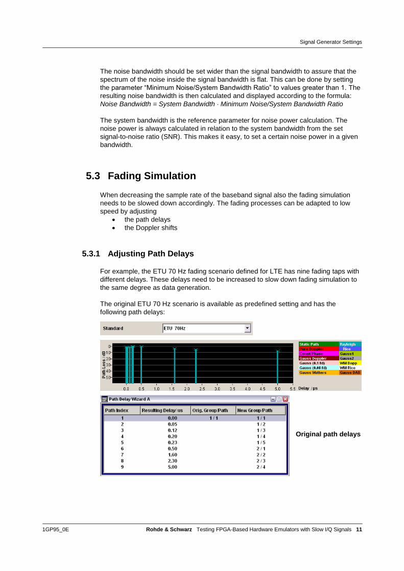
The noise bandwidth should be set wider than the signal bandwidth to assure that the
spectrum of the noise inside the signal bandwidth is flat. This can be done by setting
the parameter “Minimum Noise/System Bandwidth Ratio” to values greater than 1. The
resulting noise bandwidth is then calculated and displayed according to the formula:
Noise Bandwidth = System Bandwidth Minimum Noise/System Bandwidth Ratio
The system bandwidth is the reference parameter for noise power calculation. The
noise power is always calculated in relation to the system bandwidth from the set
signal-to-noise ratio (SNR). This makes it easy, to set a certain noise power in a given
bandwidth.
5.3 Fading Simulation
When decreasing the sample rate of the baseband signal also the fading simulation
needs to be slowed down accordingly. The fading processes can be adapted to low
speed by adjusting
the path delays
the Doppler shifts
5.3.1 Adjusting Path Delays
For example, the ETU 70 Hz fading scenario defined for LTE has nine fading taps with
different delays. These delays need to be increased to slow down fading simulation to
the same degree as data generation.
The original ETU 70 Hz scenario is available as predefined setting and has the
following path delays:
Original path delays

Signal Generator Settings
1GP95_0E Rohde & Schwarz Testing FPGA-Based Hardware Emulators with Slow I/Q Signals 12
Proceed in the following way to adjust the path delays for slow I/Q mode:
Adjust the parameter “Resulting Delay” which is the sum of the parameters “Basic
Delay” and “Additional Delay” according to the following formula:
Resulting Delay = Standard Resulting Delay N
The easiest way to configure the “Resulting Delay” is to use the “Path Delay Wizard”,
since it automatically sets the “Basic Delay” and the “Additional Delay” such that the
wanted delay is achieved.
For example, the original delays increase by the slowdown factor N = 128 to the
following values:
Slow I/Q path delays
Some fading scenarios, e.g. the ETU 70 Hz, have large delays between some of their
fading taps. For example, taps 6, 7, 8, and 9 are largely separated. In particular the last
tap has such a large delay that one fading simulator (option B14) is not sufficient any
longer to reproduce the slow I/Q fading simulation. In this case a second fading
simulator (option B15) is needed to enhance the number of available path groups from
4 to 8 (see reference [4] for details).3 To “combine” both fading simulators make the
following selection in the “Fading” block:
3 The second fading simulator (option B15) is needed to obtain the above screenshot of the “Path Delay
Wizard” showing the slow I/Q path delays for the ETU 70 Hz fading scenario.

Signal Generator Settings
1GP95_0E Rohde & Schwarz Testing FPGA-Based Hardware Emulators with Slow I/Q Signals 13
With this setting up to 8 path groups are available which makes it possible to
reproduce even fading scenarios such as the ETU 70 Hz in slow I/Q mode.
Note that the “Path Delay Wizard” configures the delay parameters only. All other settings such as the parameters “Profile” and “Path Loss” are not influenced. However, the “Path Delay Wizard” rearranges the activated taps in the path table to implement the larger delays. Therefore, after having adjusted the delays of the fading taps, adjust also the parameters “Profile” and “Path Loss” in the path table to exactly reproduce the original scenario. For example, for tap 8, change the path loss from 0 dB (default setting) to 5 dB like it is in the original fading scenario.
5.3.2 Adjusting Doppler Shifts
In addition to adjusting the path delays, also the Doppler shifts need to be adapted.
The Doppler shift is calculated from the RF frequency and the relative speed between
a transmitter and a receiver according to the following relation:
lightofSpeed
Speed
frequencyRF
shiftDoppler

Signal Generator Settings
1GP95_0E Rohde & Schwarz Testing FPGA-Based Hardware Emulators with Slow I/Q Signals 14
For example, for the ETU 70 Hz fading scenario the stipulated Doppler shift is 70 Hz.
The wanted RF frequency of the carrier signal is e.g. 2.14 GHz. To get the correct
setting for the parameter “Speed” in the path table set the RF frequency to 2.14 GHz
on the SMU. The speed is 35.3 km/h according to the above formula.
Proceed in the following way to adjust the Doppler shifts for slow I/Q mode. Follow the
steps in the given order:
In the fading menu, set the parameter “Keep Constant” to “Speed”.
This parameter determines whether the speed or the Doppler shift is kept constant
when the (virtual) RF frequency changes.
Set the parameter “Signal Dedicated To” to “Baseband Output”.
With this setting the RF frequency used by the fading simulator to calculate the
Doppler shift can be defined via the parameter “Virtual RF”.
Adjust the parameter “Virtual RF” according to the following formula:
Virtual RF = Wanted RF frequency /N
For example, the wanted RF frequency of the carrier signal is 2.14 GHz and the
slowdown factor N is 128. The parameter “Virtual RF” thus needs to be set to
16.719 MHz.
As a cross check you can take a look at the path table. The parameter “Res. Doppler
Shift” has changed from 70 Hz to 70 Hz /N = 0.547 Hz.
Note that it is not sufficient to adjust only the parameter “Res. Doppler Shift” in the path
table, since this parameter influences only the Doppler shift of the direct line of sight
signal. The adjustment of the Doppler shifts must be done via parameter “Virtual RF”,
since this parameter influences the Doppler shifts of all multipath echoes within a
(single) Rayleigh tap.

Signal Generator Settings
1GP95_0E Rohde & Schwarz Testing FPGA-Based Hardware Emulators with Slow I/Q Signals 15
5.4 Digital I/Q Output Settings
When testing hardware emulators usually the digital output of the instrument is utilized. The I/Q data (generated at Rsample) can be resampled to an output sample rate that can be defined by the user. In order not to apply any down- or up-sampling, the digital I/Q output sample rate needs to be set to the same sample rate as used in the baseband for slow I/Q signal generation.
Sample Rate Value = Rsample (slow IQ)
For example, the sample rate is set to 240 kHz.
5.5 HARQ Feedback
If real-time HARQ feedback is used in the test setup (see references [5] and [6] for details), the user can set the parameter “Additional User Delay” in units of chips (3GPP FDD) or subframes (LTE). By slowing down the baseband signal these units are also
“slowed down” accordingly, i.e. a LTE subframe is no longer 1 ms but takes 1 N milliseconds. The entered additional user delay increases therefore accordingly and does in principle not need to be adapted for slow IQ mode. However, in some test setups some fine-adjustment may become necessary. In this case, adjust the “Additional User Delay” parameter as required.

Abbreviations
1GP95_0E Rohde & Schwarz Testing FPGA-Based Hardware Emulators with Slow I/Q Signals 16
6 Abbreviations ARB Arbitrary waveform generator
AWGN Additive white Gaussian noise
BBU Baseband unit
CPRI Common public radio interface
DUT Device under test
eNodeB evolved NodeB
ETU Extended typical urban
FPGA Field-programmable gate array
GMSK Gaussian minimum shift keying
GSM Global system for mobile communication
HARQ Hybrid automatic repeat request
I/Q In-phase/quadrature
LTE 3GPP long term evolution
MIMO Multiple input multiple output
OFDM Orthogonal frequency division multiplexing
RF Radio frequency
RRH Remote radio head
UE User equipment
7 References [1] Rohde & Schwarz, R&S
®EX-IQ-BOX Digital Interface Module Operating
Manual
[2] Rohde & Schwarz, “Starting Successfully with the R&S EX-IQ-BOX”
Application Note (1MA168)
[3] Rohde & Schwarz, “CPRI RE Testing” Application Note (1GP78)
[4] Rohde & Schwarz, Fading Simulation Manual for R&S®SMU200A and
R&S®AMU200A
[5] Rohde & Schwarz, 3GPP FDD incl. enhanced MS/BS tests, HSDPA, HSUPA,
HSPA+ Digital Standard for R&S®
Signal Generators Operating Manual
[6] Rohde & Schwarz, EUTRA/LTE Digital Standard for R&S®
Signal Generators
Operating Manual
8 Ordering Information Please visit the Rohde & Schwarz product websites at www.rohde-schwarz.com for ordering information on the following Rohde & Schwarz products:
R&S®SMU200A vector signal generator
R&S®AMU200A baseband signal generator and fading simulator
R&S®SMBV100A vector signal generator
R&S®SMJ100A vector signal generator
R&S®EX-IQ-BOX digital interface module
About Rohde & Schwarz
Rohde & Schwarz is an independent group
of companies specializing in electronics. It is
a leading supplier of solutions in the fields of
test and measurement, broadcasting,
radiomonitoring and radiolocation, as well as
secure communications. Established more
than 75 years ago, Rohde & Schwarz has a
global presence and a dedicated service
network in over 70 countries. Company
headquarters are in Munich, Germany.
Environmental commitment
● Energy-efficient products
● Continuous improvement in
environmental sustainability
● ISO 14001-certified environmental
management system
Regional contact
Europe, Africa, Middle East
+49 89 4129 123 45
[email protected] North America
1-888-TEST-RSA (1-888-837-8772)
[email protected] Latin America
+1-410-910-7988
[email protected] Asia/Pacific
+65 65 13 04 88
[email protected] China
+86-800-810-8228 /+86-400-650-5896
This application note and the supplied
programs may only be used subject to the
conditions of use set forth in the download
area of the Rohde & Schwarz website.
R&S® is a registered trademark of Rohde & Schwarz GmbH & Co. KG. Trade names are trademarks of the owners.
Rohde & Schwarz GmbH & Co. KG
Mühldorfstraße 15 | D - 81671 München
Phone + 49 89 4129 - 0 | Fax + 49 89 4129 - 13777
www.rohde-schwarz.com