Embed Size (px)
Citation preview
LM79XX
REV. 03
www.apsemi.com 1
3-Terminal Negative voltage Regulators
DESCRIPTION These voltage regulators are designed as fixed negative voltage regulators for a
wide variety of applications including local, on-card regulation. Although designed
primarily as a fixed voltage regulator, these devices can be used with external
components to obtain adjustable voltages and currents.
FEATURES ■ Output current in excess of 1.0A
■ No external components required
■ Output Voltages (-5V, -6V, -8V, -9V, -10V, -12V, -15V, -18V)
■ Internal Thermal shutdown and SOA protection
■ Output voltage offered in 4% Tolerance
■ Pb-Free Packages are available
■ High ESD Level (HBM>8000V, MM>800V)
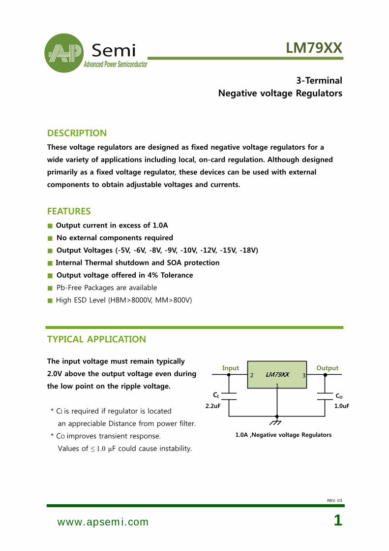
TYPICAL APPLICATION
The input voltage must remain typically
2.0V above the output voltage even during
the low point on the ripple voltage.
* CI is required if regulator is located
an appreciable Distance from power filter.
* CO improves transient response.
Values of ≤ 1.0 µF could cause instability.
Input Output
CI CO
1.0uF2.2uF
2
1
3
1.0A ,Negative voltage Regulators

LM79XX
REV. 03
www.apsemi.com 2
Maximum Ratings (TA=25 °C, unless otherwise noted)
Rating Symbol Value Unit
TO-220F TO-220 TO-252
Input Voltage -5V ~ -18V VI -35 V
-24V -40
Power Dissipation PD 2 2 1.3 W
Thermal Resistance of Junction to Ambient RθJA 65 65 92 °C/W
Thermal Resistance of Junction to Case RθJC 5 5 5 °C/W
Storage Temperature TSTG -55 ~ 125 °C
Junction Temperature TJ + 150 °C
Operating Temperature TOPR -40 ~ 125 °C
Stresses exceeding Maximum ratings may damage the device. Maximum ratings are stress ratings.
Functional operation above the recommended operating conditions is not implied.
Extended exposure to stresses the above the recommended operating conditions may affect
device reliability.
PD(max) = (TJ(max)–TA) ÷ θJA. Exceeding the maximum allowable power dissipation will result in
excessive die temperature, and the regulator will go into thermal shutdown.
Representative Schematic of LM79XX
GND
OUTPUT
INPUT
R12R13
Q16
R8
R7
Q13Q12
Q27Q26
Q9 Q10
R4 R5
Q11R6
R9
Q15
Q14
R11
R22
Q24
R21
Q22
Q23
R1 Q21
R18R15
Q8
R3
+ +
R10
D4
R20
Q17 Q19
Q18
R14 R17
D1
D2
D3
Q2 Q3
R0
Q7
Q4
Q5
Q6
R2
Q20
C2 C3
D5
+C1
R19R22A
LM79XX
REV. 03
www.apsemi.com 3
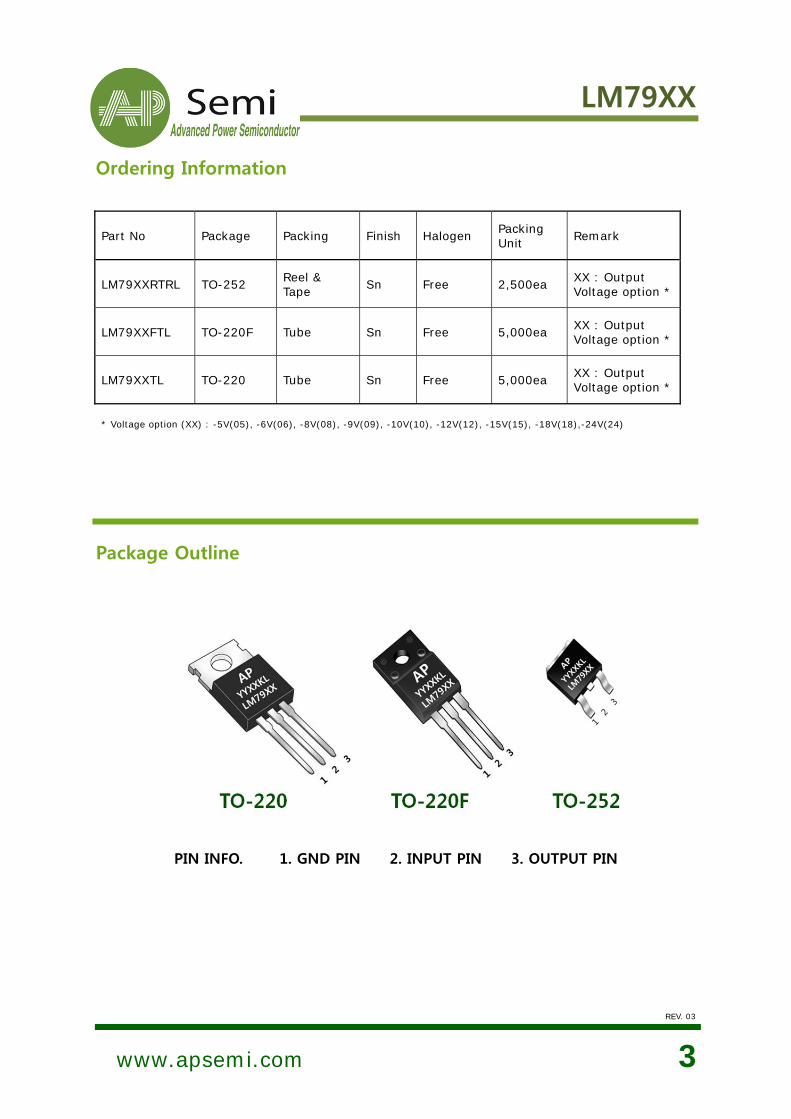
Ordering Information
Part No Package Packing Finish Halogen Packing Unit Remark
LM79XXRTRL TO-252 Reel & Tape Sn Free 2,500ea XX : Output
Voltage option *
LM79XXFTL TO-220F Tube Sn Free 5,000ea XX : Output Voltage option *
LM79XXTL TO-220 Tube Sn Free 5,000ea XX : Output Voltage option *
* Voltage option (XX) : -5V(05), -6V(06), -8V(08), -9V(09), -10V(10), -12V(12), -15V(15), -18V(18),-24V(24)
Package Outline
PIN INFO. 1. GND PIN 2. INPUT PIN 3. OUTPUT PIN
LM79XX
REV. 03
www.apsemi.com 4
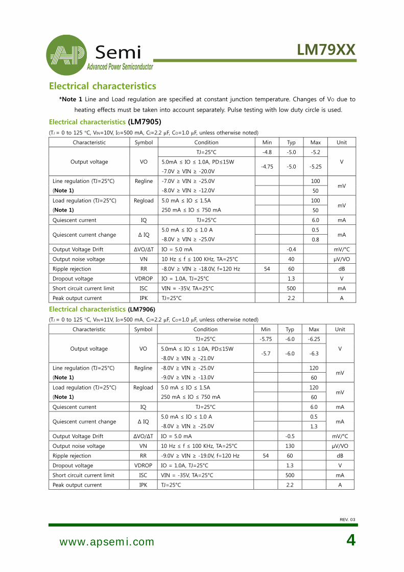
Electrical characteristics *Note 1 Line and Load regulation are specified at constant junction temperature. Changes of VO due to
heating effects must be taken into account separately. Pulse testing with low duty circle is used.
Electrical characteristics (LM7905) (TJ = 0 to 125 °C, VIN=10V, IO=500 mA, CI=2.2 µF, CO=1.0 µF, unless otherwise noted)
Characteristic Symbol Condition Min Typ Max Unit
Output voltage
VO
TJ=25°C -4.8 -5.0 -5.2
V 5.0mA ≤ IO ≤ 1.0A, PD≤15W
-7.0V ≥ VIN ≥ -20.0V -4.75 -5.0 -5.25
Line regulation (TJ=25°C)
(Note 1)
Regline -7.0V ≥ VIN ≥ -25.0V
-8.0V ≥ VIN ≥ -12.0V
100 mV
50
Load regulation (TJ=25°C)
(Note 1)
Regload 5.0 mA ≤ IO ≤ 1.5A
250 mA ≤ IO ≤ 750 mA
100 mV
50
Quiescent current IQ TJ=25°C 6.0 mA
Quiescent current change Δ IQ 5.0 mA ≤ IO ≤ 1.0 A
-8.0V ≥ VIN ≥ -25.0V
0.5 mA
0.8
Output Voltage Drift ΔVO/ΔT IO = 5.0 mA -0.4 mV/°C
Output noise voltage VN 10 Hz ≤ f ≤ 100 KHz, TA=25°C 40 µV/VO
Ripple rejection RR -8.0V ≥ VIN ≥ -18.0V, f=120 Hz 54 60 dB
Dropout voltage VDROP IO = 1.0A, TJ=25°C 1.3 V
Short circuit current limit ISC VIN = -35V, TA=25°C 500 mA
Peak output current IPK TJ=25°C 2.2 A
Electrical characteristics (LM7906)
(TJ = 0 to 125 °C, VIN=11V, IO=500 mA, CI=2.2 µF, CO=1.0 µF, unless otherwise noted)
Characteristic Symbol Condition Min Typ Max Unit
Output voltage
VO
TJ=25°C -5.75 -6.0 -6.25
V 5.0mA ≤ IO ≤ 1.0A, PD≤15W
-8.0V ≥ VIN ≥ -21.0V -5.7 -6.0 -6.3
Line regulation (TJ=25°C)
(Note 1)
Regline -8.0V ≥ VIN ≥ -25.0V
-9.0V ≥ VIN ≥ -13.0V
120 mV
60
Load regulation (TJ=25°C)
(Note 1)
Regload 5.0 mA ≤ IO ≤ 1.5A
250 mA ≤ IO ≤ 750 mA
120 mV
60
Quiescent current IQ TJ=25°C 6.0 mA
Quiescent current change Δ IQ 5.0 mA ≤ IO ≤ 1.0 A
-8.0V ≥ VIN ≥ -25.0V
0.5 mA
1.3
Output Voltage Drift ΔVO/ΔT IO = 5.0 mA -0.5 mV/°C
Output noise voltage VN 10 Hz ≤ f ≤ 100 KHz, TA=25°C 130 µV/VO
Ripple rejection RR -9.0V ≥ VIN ≥ -19.0V, f=120 Hz 54 60 dB
Dropout voltage VDROP IO = 1.0A, TJ=25°C 1.3 V
Short circuit current limit ISC VIN = -35V, TA=25°C 500 mA
Peak output current IPK TJ=25°C 2.2 A

LM79XX
REV. 03
www.apsemi.com 5
Electrical characteristics (LM7908)
(TJ = 0 to 125 °C, VIN=14V, IO=500 mA, CI=2.2 µF, CO=1.0 µF, unless otherwise noted)
Characteristic Symbol Condition Min Typ Max Unit
Output voltage
VO
TJ=25°C -7.7 -8.0 -8.3
V 5.0mA ≤ IO ≤ 1.0A, PD≤15W
-10.5V ≥ VIN ≥ -23.0V -7.6 -8.0 -8.4
Line regulation (TJ=25°C)
(Note 1)
Regline -10.5V ≥ VIN ≥ -25.0V
-11.5V ≥ VIN ≥ -17.0V
160 mV
80
Load regulation (TJ=25°C)
(Note 1)
Regload 5.0 mA ≤ IO ≤ 1.5A
250 mA ≤ IO ≤ 750 mA
160 mV
80
Quiescent current IQ TJ=25°C 6.0 mA
Quiescent current change Δ IQ 5.0 mA ≤ IO ≤ 1.0 A
-10.5V ≥ VIN ≥ -25.0V
0.5 mA
1.0
Output Voltage Drift ΔVO/ΔT IO = 5.0 mA -0.6 mV/°C
Output noise voltage VN 10 Hz ≤ f ≤ 100 KHz, TA=25°C 175 µV/VO
Ripple rejection RR -11.5V ≥VIN ≥ -21.5V, f=120 Hz 54 60 dB
Dropout voltage VDROP IO = 1.0A, TJ=25°C 1.3 V
Short circuit current limit ISC VIN = -35V, TA=25°C 500 mA
Peak output current IPK TJ=25°C 2.2 A
Electrical characteristics (LM7909)
(TJ = 0 to 125 °C, VIN=15V, IO=500 mA, CI=2.2 µF, CO=1.0 µF, unless otherwise noted)
Characteristic Symbol Condition Min Typ Max Unit
Output voltage
VO
TJ=25°C -8.65 -9.0 -9.35
V 5.0mA ≤ IO ≤ 1.0A, PD≤15W
-11.5V ≥ VIN ≥ -24.0V -8.6 -9.0 -9.4
Line regulation (TJ=25°C)
(Note 1)
Regline -11.5V ≥ VIN ≥ -25.0V
-12.0V ≥ VIN ≥ -17.0V
180 mV
90
Load regulation (TJ=25°C)
(Note 1)
Regload 5.0 mA ≤ IO ≤ 1.5A
250 mA ≤ IO ≤ 750 mA
180 mV
90
Quiescent current IQ TJ=25°C 6.0 mA
Quiescent current change Δ IQ 5.0 mA ≤ IO ≤ 1.0 A
-11.5V ≥ VIN ≥ -26.0V
0.5 mA
1.0
Output Voltage Drift ΔVO/ΔT IO = 5.0 mA -0.6 mV/°C
Output noise voltage VN 10 Hz ≤ f ≤ 100 KHz, TA=25°C 175 µV/VO
Ripple rejection RR -13.0V ≥VIN ≥ -23.0V, f=120 Hz 54 60 dB
Dropout voltage VDROP IO = 1.0A, TJ=25°C 1.3 V
Short circuit current limit ISC VIN = -35V, TA=25°C 500 mA
Peak output current IPK TJ=25°C 2.2 A
LM79XX
REV. 03
www.apsemi.com 6
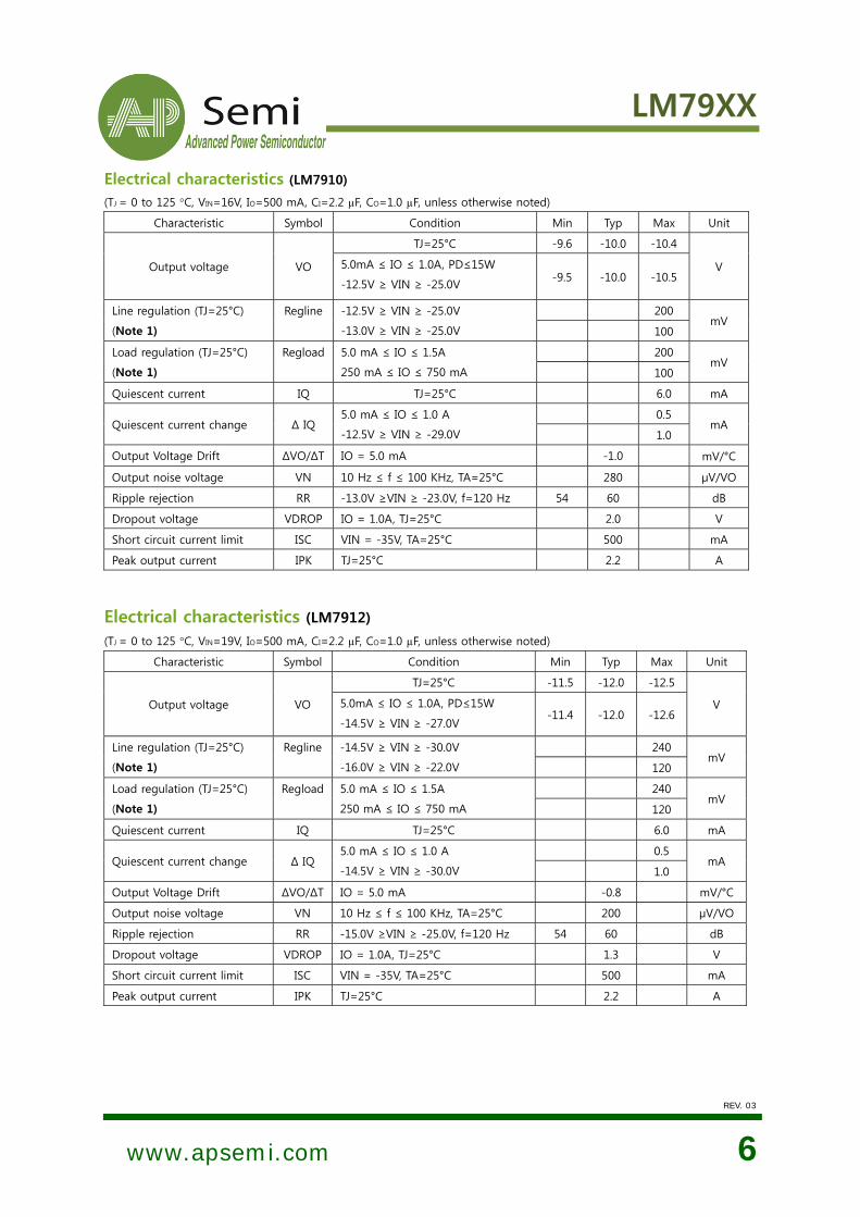
Electrical characteristics (LM7910)
(TJ = 0 to 125 °C, VIN=16V, IO=500 mA, CI=2.2 µF, CO=1.0 µF, unless otherwise noted)
Characteristic Symbol Condition Min Typ Max Unit
Output voltage
VO
TJ=25°C -9.6 -10.0 -10.4
V 5.0mA ≤ IO ≤ 1.0A, PD≤15W
-12.5V ≥ VIN ≥ -25.0V -9.5 -10.0 -10.5
Line regulation (TJ=25°C)
(Note 1)
Regline -12.5V ≥ VIN ≥ -25.0V
-13.0V ≥ VIN ≥ -25.0V
200 mV
100
Load regulation (TJ=25°C)
(Note 1)
Regload 5.0 mA ≤ IO ≤ 1.5A
250 mA ≤ IO ≤ 750 mA
200 mV
100
Quiescent current IQ TJ=25°C 6.0 mA
Quiescent current change Δ IQ 5.0 mA ≤ IO ≤ 1.0 A
-12.5V ≥ VIN ≥ -29.0V
0.5 mA
1.0
Output Voltage Drift ΔVO/ΔT IO = 5.0 mA -1.0 mV/°C
Output noise voltage VN 10 Hz ≤ f ≤ 100 KHz, TA=25°C 280 µV/VO
Ripple rejection RR -13.0V ≥VIN ≥ -23.0V, f=120 Hz 54 60 dB
Dropout voltage VDROP IO = 1.0A, TJ=25°C 2.0 V
Short circuit current limit ISC VIN = -35V, TA=25°C 500 mA
Peak output current IPK TJ=25°C 2.2 A
Electrical characteristics (LM7912)
(TJ = 0 to 125 °C, VIN=19V, IO=500 mA, CI=2.2 µF, CO=1.0 µF, unless otherwise noted)
Characteristic Symbol Condition Min Typ Max Unit
Output voltage
VO
TJ=25°C -11.5 -12.0 -12.5
V 5.0mA ≤ IO ≤ 1.0A, PD≤15W
-14.5V ≥ VIN ≥ -27.0V -11.4 -12.0 -12.6
Line regulation (TJ=25°C)
(Note 1)
Regline -14.5V ≥ VIN ≥ -30.0V
-16.0V ≥ VIN ≥ -22.0V
240 mV
120
Load regulation (TJ=25°C)
(Note 1)
Regload 5.0 mA ≤ IO ≤ 1.5A
250 mA ≤ IO ≤ 750 mA
240 mV
120
Quiescent current IQ TJ=25°C 6.0 mA
Quiescent current change Δ IQ 5.0 mA ≤ IO ≤ 1.0 A
-14.5V ≥ VIN ≥ -30.0V
0.5 mA
1.0
Output Voltage Drift ΔVO/ΔT IO = 5.0 mA -0.8 mV/°C
Output noise voltage VN 10 Hz ≤ f ≤ 100 KHz, TA=25°C 200 µV/VO
Ripple rejection RR -15.0V ≥VIN ≥ -25.0V, f=120 Hz 54 60 dB
Dropout voltage VDROP IO = 1.0A, TJ=25°C 1.3 V
Short circuit current limit ISC VIN = -35V, TA=25°C 500 mA
Peak output current IPK TJ=25°C 2.2 A
LM79XX
REV. 03
www.apsemi.com 7
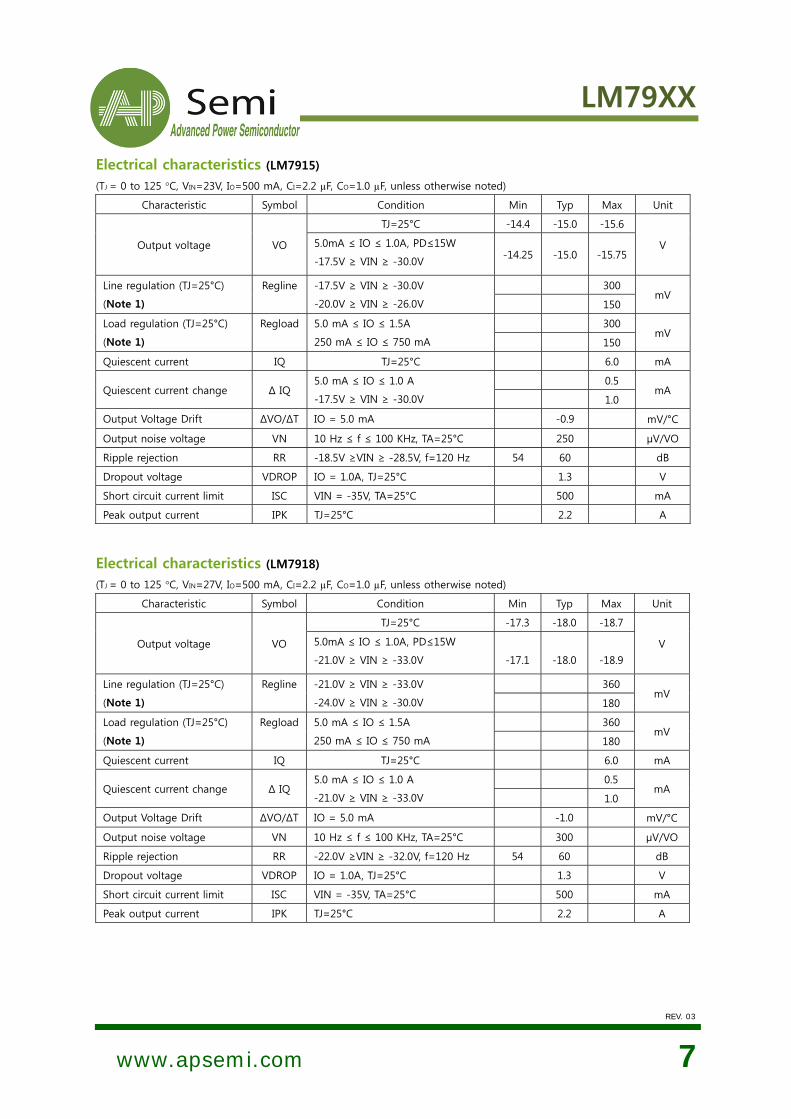
Electrical characteristics (LM7915)
(TJ = 0 to 125 °C, VIN=23V, IO=500 mA, CI=2.2 µF, CO=1.0 µF, unless otherwise noted)
Characteristic Symbol Condition Min Typ Max Unit
Output voltage
VO
TJ=25°C -14.4 -15.0 -15.6
V 5.0mA ≤ IO ≤ 1.0A, PD≤15W
-17.5V ≥ VIN ≥ -30.0V -14.25 -15.0 -15.75
Line regulation (TJ=25°C)
(Note 1)
Regline -17.5V ≥ VIN ≥ -30.0V
-20.0V ≥ VIN ≥ -26.0V
300 mV
150
Load regulation (TJ=25°C)
(Note 1)
Regload 5.0 mA ≤ IO ≤ 1.5A
250 mA ≤ IO ≤ 750 mA
300 mV
150
Quiescent current IQ TJ=25°C 6.0 mA
Quiescent current change Δ IQ 5.0 mA ≤ IO ≤ 1.0 A
-17.5V ≥ VIN ≥ -30.0V
0.5 mA
1.0
Output Voltage Drift ΔVO/ΔT IO = 5.0 mA -0.9 mV/°C
Output noise voltage VN 10 Hz ≤ f ≤ 100 KHz, TA=25°C 250 µV/VO
Ripple rejection RR -18.5V ≥VIN ≥ -28.5V, f=120 Hz 54 60 dB
Dropout voltage VDROP IO = 1.0A, TJ=25°C 1.3 V
Short circuit current limit ISC VIN = -35V, TA=25°C 500 mA
Peak output current IPK TJ=25°C 2.2 A
Electrical characteristics (LM7918)
(TJ = 0 to 125 °C, VIN=27V, IO=500 mA, CI=2.2 µF, CO=1.0 µF, unless otherwise noted)
Characteristic Symbol Condition Min Typ Max Unit
Output voltage
VO
TJ=25°C -17.3 -18.0 -18.7
V 5.0mA ≤ IO ≤ 1.0A, PD≤15W
-21.0V ≥ VIN ≥ -33.0V
-17.1
-18.0
-18.9
Line regulation (TJ=25°C)
(Note 1)
Regline -21.0V ≥ VIN ≥ -33.0V
-24.0V ≥ VIN ≥ -30.0V
360 mV
180
Load regulation (TJ=25°C)
(Note 1)
Regload 5.0 mA ≤ IO ≤ 1.5A
250 mA ≤ IO ≤ 750 mA
360 mV
180
Quiescent current IQ TJ=25°C 6.0 mA
Quiescent current change Δ IQ 5.0 mA ≤ IO ≤ 1.0 A
-21.0V ≥ VIN ≥ -33.0V
0.5 mA
1.0
Output Voltage Drift ΔVO/ΔT IO = 5.0 mA -1.0 mV/°C
Output noise voltage VN 10 Hz ≤ f ≤ 100 KHz, TA=25°C 300 µV/VO
Ripple rejection RR -22.0V ≥VIN ≥ -32.0V, f=120 Hz 54 60 dB
Dropout voltage VDROP IO = 1.0A, TJ=25°C 1.3 V
Short circuit current limit ISC VIN = -35V, TA=25°C 500 mA
Peak output current IPK TJ=25°C 2.2 A
LM79XX
REV. 03
www.apsemi.com 8
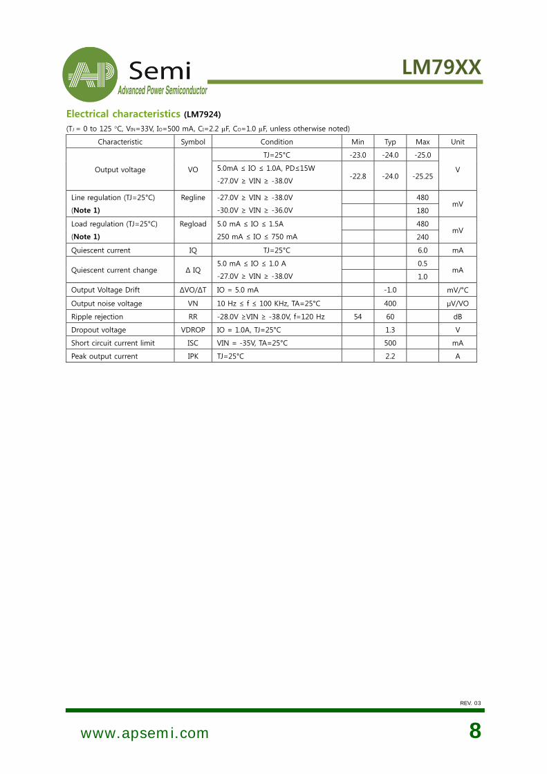
Electrical characteristics (LM7924)
(TJ = 0 to 125 °C, VIN=33V, IO=500 mA, CI=2.2 µF, CO=1.0 µF, unless otherwise noted)
Characteristic Symbol Condition Min Typ Max Unit
Output voltage
VO
TJ=25°C -23.0 -24.0 -25.0
V 5.0mA ≤ IO ≤ 1.0A, PD≤15W
-27.0V ≥ VIN ≥ -38.0V -22.8 -24.0 -25.25
Line regulation (TJ=25°C)
(Note 1)
Regline -27.0V ≥ VIN ≥ -38.0V
-30.0V ≥ VIN ≥ -36.0V
480 mV
180
Load regulation (TJ=25°C)
(Note 1)
Regload 5.0 mA ≤ IO ≤ 1.5A
250 mA ≤ IO ≤ 750 mA
480 mV
240
Quiescent current IQ TJ=25°C 6.0 mA
Quiescent current change Δ IQ 5.0 mA ≤ IO ≤ 1.0 A
-27.0V ≥ VIN ≥ -38.0V
0.5 mA
1.0
Output Voltage Drift ΔVO/ΔT IO = 5.0 mA -1.0 mV/°C
Output noise voltage VN 10 Hz ≤ f ≤ 100 KHz, TA=25°C 400 µV/VO
Ripple rejection RR -28.0V ≥VIN ≥ -38.0V, f=120 Hz 54 60 dB
Dropout voltage VDROP IO = 1.0A, TJ=25°C 1.3 V
Short circuit current limit ISC VIN = -35V, TA=25°C 500 mA
Peak output current IPK TJ=25°C 2.2 A
LM79XX
REV. 03
www.apsemi.com 9
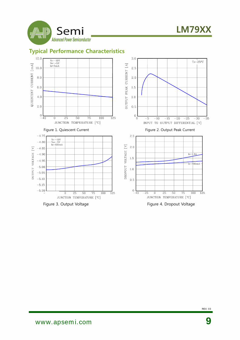
Typical Performance Characteristics
Figure 1. Quiescent Current Figure 2. Output Peak Current
Figure 3. Output Voltage Figure 4. Dropout Voltage

LM79XX
REV. 03
www.apsemi.com 10
Typical Applications
NA7905-20VInput
VO ≤ 10V
CI CO
1µF1 µF
R
IO = 5.0 / R + IQ
1
2 3
Figure 4-1 Constant Current Regulator
NA7815+20VInput
+15VOutput
CI CO
1 µF0.33µF
1
2
3
NA7915-20VInput
1.0 µF
1.0 µF1
2 3
-15VOutput
1.0 µF
Figure 4-2 Operation Amplifier Supply (±15V @ 1.0A)
LM7905
LM7815
LM7915
LM79XX
REV. 03
www.apsemi.com 11
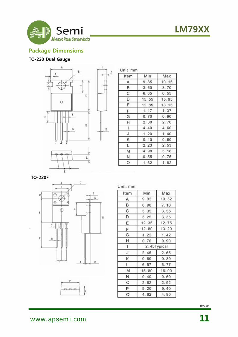
Package Dimensions TO-220 Dual Gauge
TO-220F
.

LM79XX
REV. 03
www.apsemi.com 12
Package Dimensions TO-252
LM79XX
REV. 03
www.apsemi.com 13
Revision History
No Date Contents
1 2015-01-30 Initial Brief Datasheet Release
2 2015-06-22 ESD Level Update
3 2016-11-07 Power Dissipation Update
LM79XX
REV. 03
www.apsemi.com 14
http://www.apsemi.com
IMPORTANT NOTICE
AP Semiconductor co, Ltd reserves the right to make changes without further notice to any products or specifications herein. AP Semiconductor co, Ltd does not assume any responsibility for use of any its products for any particular purpose, nor does AP Semiconductor co, Ltd assume any liability arising out of the application or use of any its products or circuits. AP Semiconductor co, Ltd does not convey any license under its patent rights or other rights nor the rights of others.
AP Semiconductor Co., Ltd Contact. Tel 82.70.4693.2299 FAX 82.70.4000.4009
E-mail: [email protected]
© 2015 AP semiconductor Co., Ltd. –Printed in KOREA –All Rights Reserved.