Embed Size (px)
Citation preview
An LTCC Based Compact SIW Antenna Array Feed Network for a Passive Imaging Radiometer
by
Hattan Abuzaid
A Thesis Submitted in Partial Fulfillment of the Requirements for the Degree of
Master of Science
in Electrical Engineering
at King Abdullah University of Science and Technology
February 2013

ii
ABSTRACT
Passive millimeter-wave (PMMW) imaging is a technique that allows the detection of inherent
millimeter-wave radiation emitted by bodies. Since different bodies with varying properties emit
unequal power intensities, a contrast can be established to detect their presence. The advantage
of this imaging scheme over other techniques, such as optical and infrared imaging, is its ability
to operate under all weather conditions. This is because the relatively long wavelengths of
millimeter-waves, as compared to visible light, penetrate through clouds, fog, and sandstorms.
The core of a PMMW camera is an antenna, which receives the electromagnetic radiation from a
scene. Because PMMW systems require high gains to operate, large antenna arrays are typically
employed. This mandatory increase of antenna elements is associated with a large feeding
network. Therefore, PMMW cameras usually have a big profile.
In this work, two enabling technologies, namely, Substrate integrated Waveguide (SIW) and
Low Temperature Co-fired Ceramic (LTCC), are coupled with an innovative design to
miniaturize the passive front-end. The two technologies synergize very well with the shielded
characteristics of SIW and the high density multilayer integration of LTCC. The proposed design
involves a novel multilayer power divider, which is incorporated in a folded feed network
structure by moving between layers. The end result is an efficient feeding network, which
footprint is least affected by an increase in array size. This is because the addition of more
elements is accommodated by a vertical expansion rather than a lateral one.
To characterize the feed network, an antenna array has been designed and integrated through
efficienct transitions.The complete structure has been simulated and fabricated. The results
demonstrate an excellent performance, manifesting in a gain of 20 dBi and a bandwidth of more
than 11.4% at 35 GHz. These values satisfy the general requirements of a PMMW system.

iii
ACKNOWLEDGMENTS
First of all, I would like to express my gratitude to my advisor Dr. Atif Shamim for his
understanding, patience, and motivation. I would also like to thank my thesis committee
members: Dr. Hakan Bagci and Dr. Ian Foulds for dedicating their time to mend and improve
this thesis.
My sincere thanks also goes to Prof. Ke Wu of the University of Montreal and his PhD student
Ali Doghri, for providing me with a summer research opportunity at Poly Grames research
center, where I completed part of the work. They also have my appreciation for providing help in
fabrication and characterization.
Moreover, I thank my colleagues in IMPACT lab for their fruitful discussions and continuous
help and support.
Last but not least, I thank my family for their unconditional love and care.

iv
TABLE OF CONTENTS
ABSTRACT .................................................................................................................................... ii
ACKNOWLEDGMENTS ............................................................................................................. iii
LIST OF TABLES ......................................................................................................................... vi
LIST OF FIGURES ...................................................................................................................... vii
LIST OF ACRONYMS ................................................................................................................ xii
1 Introduction ............................................................................................................................. 1
1.1 Objectives ......................................................................................................................... 2
1.2 Challenges ........................................................................................................................ 3
1.3 Contributions .................................................................................................................... 4
1.4 Thesis Organization.......................................................................................................... 5
2 Literature Review.................................................................................................................... 6
2.1 Theory of PMMW Imaging.............................................................................................. 6
2.2 SIW Technology ............................................................................................................ 13
2.3 LTCC Technology.......................................................................................................... 16
2.4 Integrated SIW Millimeter-Wave Antenna Arrays ........................................................ 18
3 Antenna Array Feeding Network Design ............................................................................. 21
3.1 SIW Design Consideration ............................................................................................. 21
3.1.1 SIW and Its Equivalent Rectangular Waveguide (RWG)....................................... 21
3.1.2 Choosing SIW Line Parameters .............................................................................. 22
3.2 Beamforming Network Design Considerations ............................................................. 26
3.3 Feeding Network Components ....................................................................................... 29
3.3.1 Power Divider ......................................................................................................... 30

v
3.3.2 H-Plane Bend .......................................................................................................... 39
3.3.3 Microstrip-to-SIW Transition ................................................................................. 44
3.4 Feeding Network Architecture ....................................................................................... 48
3.5 Feeding Network Simulation Results ............................................................................. 52
4 Antenna Integration .............................................................................................................. 56
4.1 LTCC Antenna ............................................................................................................... 56
4.2 Rogers Antenna .............................................................................................................. 61
4.3 Integration of the Feeding Network and the Antenna Array .......................................... 68
4.3.1 Transverse Slot Coupling ........................................................................................ 68
4.3.2 Waveguide Impedance Transformer ....................................................................... 71
4.4 Full Passive Front-End ................................................................................................... 75
5 Conclusion ............................................................................................................................ 83
5.1 Conclusions .................................................................................................................... 83
5.2 Future Work ................................................................................................................... 83
References ..................................................................................................................................... 85

vi
LIST OF TABLES
Table 2-1: Effective emissivity of various materials at 44, 94, and 140 GHz. ............................... 8
Table 2-2: Several factors that influence the quality of a PMMW image and their corresponding
impact. ........................................................................................................................................... 11
Table 2-3: A variety of microwave SIW components. ................................................................. 15
Table 2-4: DuPont 9K7 GreenTape properties ............................................................................. 18
Table 2-5: Survey of previous integration of wide-band, high-gain SIW antenna arrays. ........... 19
Table 3-1: Schemes for linear antenna array radiation pattern synthesis using non-equal
amplitude excitation. ..................................................................................................................... 29
Table 3-2: Return loss of the investigated H-plane geometries. ................................................... 42
Table 3-3: Parameters of the optimized microstrip-to-SIW transition. ........................................ 46
Table 3-4: Complete feeding network amplitude excitation coefficients. .................................... 55
Table 4-1: Parameters of the optimized H-plane dielectric loaded SIW horn. ............................. 58
Table 4-2: Pros and cons of the attempted LTCC antenna designs. ............................................. 62
Table 4-3: Parameters of the optimized exponentially tapered slot antenna on Duroid 5880. ..... 64
Table 4-4: Parameters of the proposed transition from DuPont 9K7 to Rogers Duroid 5880...... 69
Table 4-5: Parameters of the proposed four-section impedance transformer. .............................. 73
Table 4-6: A comparison between the presented passive front-end and SIW implementations of
integrated antenna arrays. ............................................................................................................. 82

vii
LIST OF FIGURES
Figure 2-1: The attenuation of propagating electromagnetic waves in different regimes under
neutral (red line) and disturbed (black lines) weather conditions. .................................................. 7
Figure 2-2: An illustration of different PMMW scene constituents. .............................................. 8
Figure 2-3: Visible and PMMW images of a runway as seen by a pilot before touchdown: (a) and
(c) show visible images in clear and foggy weather; (b) and (d) show the corresponding PMMW
images. ............................................................................................................................................ 9
Figure 2-4: A visual image (a) along with its corresponding 94 GHz PMMW image taken with
different aperture sizes: (b) 48, (c) 24, and (d) 12 inch. ............................................................... 10
Figure 2-5: Schematic of different types of imaging systems (a) mechanically-scanned single
element; (b) focal plane array; (c) multi-element interferometer; (d) phased array. .................... 12
Figure 2-6: SIW and the equivalent RWG. ................................................................................... 14
Figure 2-7: A comparison of the attenuation constants of Microstrip line, SIW, Multilayered
SIW, and RWG. ............................................................................................................................ 14
Figure 2-8: A schematic cross-section of a model LTCC module................................................ 16
Figure 2-9: LTCC manufacturing process flow diagram. ............................................................. 17
Figure 2-10: Front and backsides of 4 x 8 element PCB-WG-fed array. ..................................... 20
Figure 2-11: Photographs of the manufactured LTCC chain array. (a) antenna side, (b) SIW side.
....................................................................................................................................................... 20
Figure 2-12: Photograph of the cavity array antenna on LTCC (left: top view, right: bottom
view). ............................................................................................................................................ 20
Figure 2-13: Manufactured dielectric rod antenna array. ............................................................. 20
Figure 2-14: Photograph of the fabricated 1 x 16 SIW corrugated Fermi-TSA linear array. ....... 20

viii
Figure 3-1: Cut-off frequencies of the TE10-like and TE20-like modes of the straight pattern SIW
versus W and D. ............................................................................................................................ 23
Figure 3-2: Comparison of the dispersion curves of an SIW with an equivalent rectangular
waveguide. .................................................................................................................................... 23
Figure 3-3: Leakage losses varying from 10-6 to 10-2 Np/rad as functions of post diameter and
period length normalized to the cutoff wavelength. ..................................................................... 24
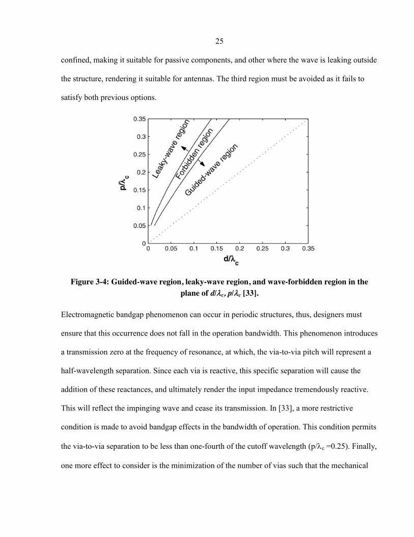
Figure 3-4: Guided-wave region, leaky-wave region, and wave-forbidden region in the plane of
d/c, p/c........................................................................................................................................ 25
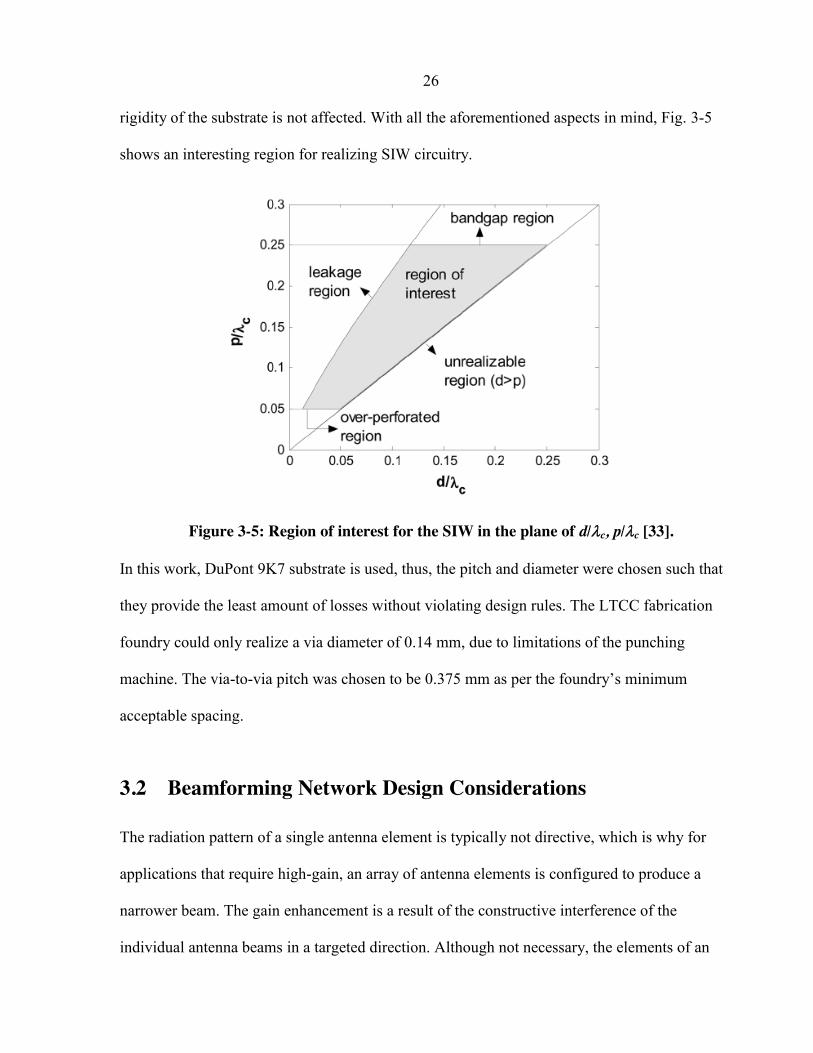
Figure 3-5: Region of interest for the SIW in the plane of d/c, p/c. .......................................... 26
Figure 3-6: Three-dimensional antenna pattern of a planar array of isotropic elements with a
spacing of dx = dy = λ/2, and equal amplitude and phase excitations. .......................................... 28
Figure 3-7: An illustration of the typical components which form an SIW feeding network. ..... 30
Figure 3-8: Geometry of (a) SIW and (b) Folded SIW. ................................................................ 31
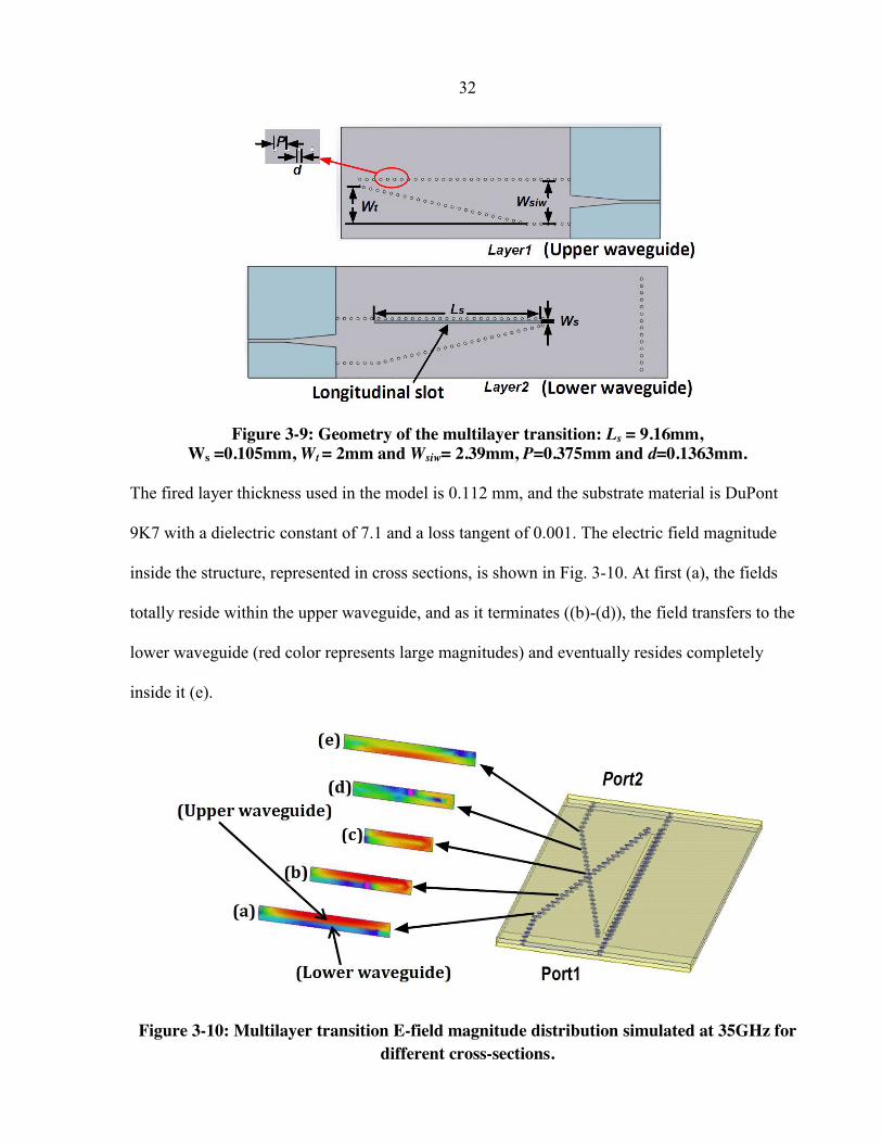
Figure 3-9: Geometry of the multilayer transition: Ls = 9.16mm, Ws =0.105mm, Wt = 2mm and
Wsiw= 2.39mm ............................................................................................................................... 32
Figure 3-10: Multilayer transition E-field magnitude distribution simulated at 35GHz for
different cross-sections. ................................................................................................................ 32
Figure 3-11: Fabricated multilayer transition. .............................................................................. 33
Figure 3-12: Measured and simulated return loss of the proposed multilayer transition. ............ 34
Figure 3-13: Measured and simulated insertion loss of the proposed multilayer transition. ........ 34
Figure 3-14: Geometry of the multilayer 3-dB power divider: Ls = 9.16mm, Ws =0.105mm, Wt =
2mm and Wsiw= 2.39mm. .............................................................................................................. 35
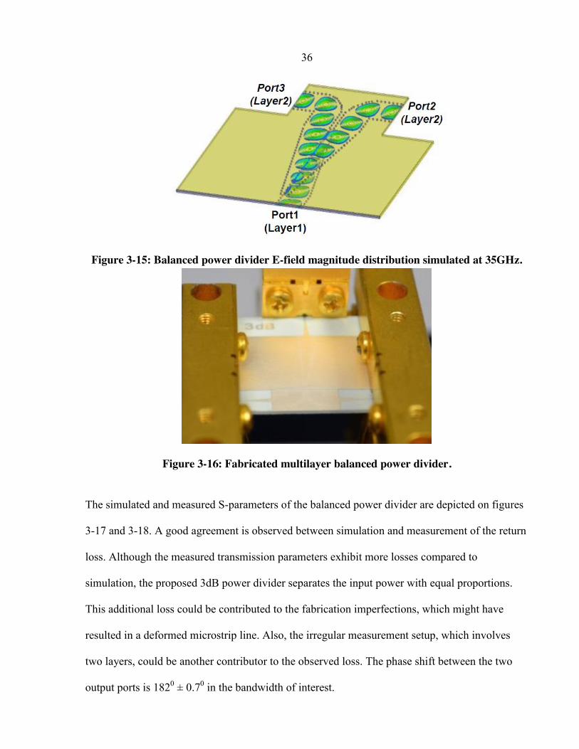
Figure 3-15: Balanced power divider E-field magnitude distribution simulated at 35GHz. ........ 36
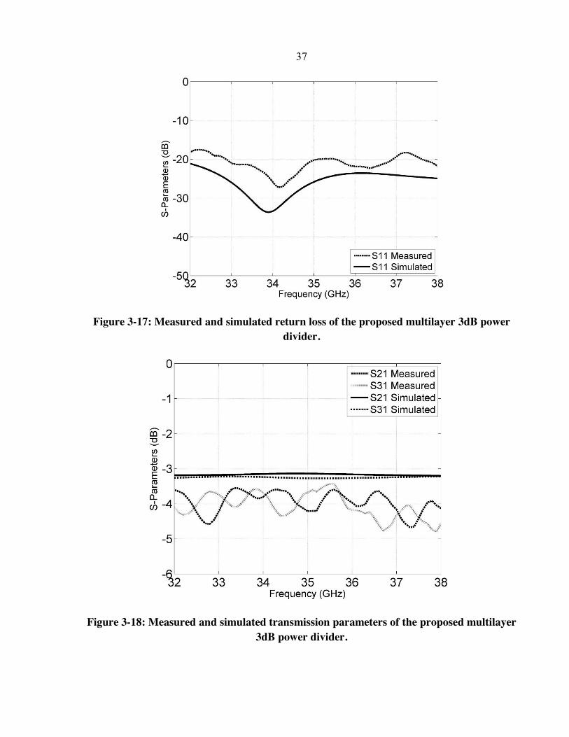
Figure 3-16: Fabricated multilayer balanced power divider. ........................................................ 36

ix
Figure 3-17: Measured and simulated return loss of the proposed multilayer 3dB power divider.
....................................................................................................................................................... 37
Figure 3-18: Measured and simulated transmission parameters of the proposed multilayer 3dB
power divider. ............................................................................................................................... 37
Figure 3-19: Top view of the second layer in the arbitrary power divider with an illustration of
the “offset” concept....................................................................................................................... 38
Figure 3-20: Simulated return loss of the proposed multilayer arbitrary power divider (offset =
1.1mm). ......................................................................................................................................... 39
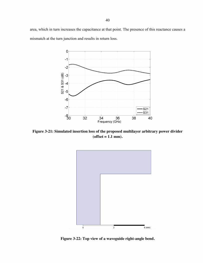
Figure 3-21: Simulated insertion loss of the proposed multilayer arbitrary power divider (offset =
1.1 mm). ........................................................................................................................................ 40
Figure 3-22: Top view of a waveguide right-angle bend. ............................................................. 40
Figure 3-23: Top view of the investigated H-plane geometries. (a) single-cut miter, (b) three-cut
miter, and (c) inductive post placement. ....................................................................................... 42
Figure 3-24: Top view of the via-hole implementation of the three-cut miter H-plane bend. ..... 43
Figure 3-25: Simulated return loss of the SIW three-cut miter H-plane bend. ............................. 43
Figure 3-26: Simulated insertion loss of the SIW three-cut miter H-plane bend. ........................ 44
Figure 3-27: Configuration of the microstrip-to-SIW transition. ................................................. 45
Figure 3-28: Dominant modal electric field profiles (a) in rectangular waveguide and (b) in
microstrip line. .............................................................................................................................. 45
Figure 3-29: Simulation model of the designed microstrip-to-SIW transition. ............................ 46
Figure 3-30: Return loss of the optimized microstrip-to-SIW transition. ..................................... 47
Figure 3-31: Insertion loss of the optimized microstrip-to-SIW transition. ................................. 47
Figure 3-32: Half-array topology of quasi-triangular power distribution. α denotes the voltage
division ratio of each stage. .......................................................................................................... 49

x
Figure 3-33: Array factor of 10 array elements spaced by 0.5λo and excited by the distribution
defined in Fig. 3-32. ...................................................................................................................... 49
Figure 3-34: SIW implementation of a 10-element array using quasi-triangular distribution. .... 50
Figure 3-35: Proposed Feed Architecture (modification to the distribution in Fig. 3-32). ........... 51
Figure 3-36: Multilayer schematic of the proposed feeding network. .......................................... 51
Figure 3-37: Implementation of the proposed feeding network. The intermittent blue boxes
illustrate the interaction between the different layers. .................................................................. 52
Figure 3-38: Simulation model of the half feeding network......................................................... 53
Figure 3-39: Transmission parameters of the half feeding network. ............................................ 53
Figure 3-40: Phase difference between the output ports of the half feeding network. ................. 54
Figure 3-41: Projected beam shape of a 10-element array with a spacing of 0.92 λo. .................. 55
Figure 4-1: Configuration of the H-plane SIW horn antenna. ...................................................... 57
Figure 4-2: The optimized H-plane dielectric loaded SIW horn. ................................................. 58
Figure 4-3: Return loss of the optimized H-plane dielectric loaded SIW horn. ........................... 59
Figure 4-4: 3D radiation pattern of the optimized H-plane dielectric loaded SIW horn antenna. 59
Figure 4-5: Attempted corrugated linearly tapered slot antenna on DuPont 9K7. ....................... 60
Figure 4-6: The attempted waveguide fed 1 x 4 LTCC DRA....................................................... 61
Figure 4-7: Three types of endfire tapered slot antennas. A dielectric rod antenna is shown for
comparison. ................................................................................................................................... 63
Figure 4-8: The optimized exponentially tapered slot antenna on Duroid 5880. ......................... 65
Figure 4-9: Return loss of the TSA on Duroid 5880. ................................................................... 66
Figure 4-10: 3D radiation pattern of the TSA on Duroid 5880. ................................................... 66
Figure 4-11: Proposed TSA 10-element array on Duroid 5880. ................................................... 67
Figure 4-12: 3D radiation pattern of the proposed TSA 10-element array. .................................. 67

xi
Figure 4-13: Mutual coupling between two non-peripheral elements in the proposed TSA 10-
element array. ................................................................................................................................ 68
Figure 4-14: Configuration of the proposed transition from DuPont 9K7 to Rogers Duroid 5880.
....................................................................................................................................................... 69
Figure 4-15: Return loss of the proposed transition from DuPont 9K7 to Rogers Duroid 5880. . 70
Figure 4-16: Insertion loss of the proposed transition from DuPont 9K7 to Rogers Duroid 5880.
....................................................................................................................................................... 70
Figure 4-17: Schematic circuit of a multi-section λ/4 impedance transformer............................. 71
Figure 4-18: The proposed four-section impedance transformer simulation model using
equivalent RWG. The electric field magnitude inside the structure is also shown. ..................... 73
Figure 4-19: SIW implementation of the proposed impedance transformer. ............................... 73
Figure 4-20: Return loss of the proposed impedance transformer. ............................................... 74
Figure 4-21: Insertion loss of the proposed impedance transformer. ........................................... 74
Figure 4-22: Full integrated passive front-end.............................................................................. 76
Figure 4-23: 3D realized gain of the passive front-end. ............................................................... 76
Figure 4-24: Simulated return loss of the passive front-end. ........................................................ 77
Figure 4-25: Passive front-end radiation efficiency...................................................................... 77
Figure 4-26: Passive front-end H-plane radiation pattern at 35 GHz. .......................................... 78
Figure 4-27: Passive front-end H-plane radiation pattern at 33 GHz. .......................................... 78
Figure 4-28: Passive front-end H-plane radiation pattern at 37 GHz. .......................................... 79
Figure 4-29: Passive front-end E-plane radiation pattern at 35 GHz............................................ 79
Figure 4-30: Fabricated passive front-end side view. ................................................................... 81
Figure 4-31: Fabricated passive front-end back view. .................................................................. 81
Figure 4-32: Simulated versus measured return loss of the full structure. ................................... 82

xii
LIST OF ACRONYMS
Acronym Description PMMW Passive Millimeter-Wave
SIW Substrate Integrated Waveguide FSIW Folded Substrate Integrated Waveguide MSIW Multilayered Substrate Integrated Waveguide RWG Rectangular Waveguide MS Microstrip PCB Printed Circuit Board
LTCC Low Temperature Co-fired Ceramic 3D Three Dimensional
LCP Liquid Crystalline Polymer

1
1 Introduction
Passive millimeter wave (PMMW) imaging is a technique to form an image of a scene by
utilizing the inherent radiation of bodies in the millimeter wave regime [1]. This emission
phenomenon, known as black body radiation, is associated with any object characterized by a
temperature above absolute zero. The relatively large wavelengths of millimeter waves, when
compared to visible light, allow it to penetrate through fog, clouds, rain, and sandstorms,
rendering PMMW imaging systems operable in low-visibility conditions. This ability to see in
almost any type of weather can turn previously unfavorable situations into harmless or even
beneficial ones. PMMW cameras could be used for commercial aircraft landing assistance in
airports that suffer from frequent sandstorms or fog. Also, coupled with their passive nature, they
could be used to “silently” detect targets in military operations. In addition, the fact that these
cameras are able to penetrate through clothing but remain nonintrusive to human bodies makes
them a great candidate for security surveillance applications, imaging concealed weapons, for
example, detecting objects that are missed by other technologies. A final mention, with many yet
unlisted, is their ability to monitor the spatial distribution of soil moisture content and snow
water content, which is imperative to the fields of agriculture, hydrology, and meteorology [2].
The imaging is performed at low atmospheric attenuation windows at 35, 94, 140, and 220 GHz.
Although this type of imaging has been practiced for decades [1], the advent and improvement of
technologies has rekindled interest in it; advances in active circuits components and the creation
of transistors with high cut-off frequencies has enabled the exploitation of higher frequencies to
perform the imaging. This yields high-resolution pictures refreshed at video rates [3], as well as

2
devices that are small enough to be mobile. However, the stringent requirements of PMMW
imaging systems pose quite a number of challenges to be tackled in order to achieve mass-
producible, low profile, and low cost systems. These challenges include but are not limited to,
forming a complete system using as few platforms as possible to pave the path to true monolithic
integration, miniaturizing the passive front-end which in typical cases occupies the majority of a
radio chip, and realizing efficient active circuitry that operates in the upper-frequency spectrum
of the millimeter wave regime.
1.1 Objectives
As with any other imaging system, the knowledge needed to design a complete PMMW camera
falls under different specialized disciplines, namely, passive electromagnetic components, active
circuitry, and signal processing. The work in this thesis will revolve around the passive front-
end, which includes the antenna array and the feeding associated with it, this feeding network
usually occupies a large amount of space, which increases significantly with the addition of more
antenna elements. Other parts of the system will be discussed, to a lesser extent, for the purpose
of reaching a design that is system-compliant. The main objectives can be summarized in the
following list:
To create a 35 GHz feeding network that is compact while maintaining high performance
efficiency. The size of the network should be least affected by increasing the number of
antenna elements.
To test the feeding network by connecting it to a designed 35 GHz antenna array which is
suitable for this application. The passive front-end is then tested to extract its
performance.

3
To exploit the multilayer nature of Low Temperature Co-fired Ceramic (LTCC)
technology [4], which enables vertical integration and the miniaturization of lateral
dimensions.
To use Substrate Integrated Waveguide (SIW) technology [5] as a basis for component
design to take advantage of its excellent high-frequency characteristics and its synergy
with multilayer structures.
The work done in this thesis is an effort to make a miniaturized, low cost, system-compliant,
passive front-end, and ultimately hasten the advent of a monolithic PMMW imaging camera.
1.2 Challenges
There are a number of challenges associated with the proposed work. These challenges are
discussed below.
Since the PMMW camera is designed to detect inherent body radiation which has an
extremely low power level, the antenna has to provide a significant amount of gain,
typically, this is achieved through increasing the physical size of the front-end, which
contradicts with the goal of a miniaturized system. Thus, this paradox needs to be solved
using design innovation.
The sensitivity of a PMMW imaging system is directly proportional to its bandwidth [6];
in other words, a larger bandwidth yields more sensitivity, that is the ability of the system
to detect subtle variations in the scene. The system gain response must be as flat as
possible within this bandwidth. Evidently, achieving this is very challenging since all the
components in the design are frequency-dependent.

4
LTCC fabrication, in contrast to other fabrication media, such as Printed Circuit Board
(PCB), has a strict set of rules to be followed, as well as limitations on the physical
properties of the structure. This hinders the degree of freedom in the design and limits the
pool of feasible structures.
The passive front-end integration with a PMMW system to form an image requires the
designed structure to be compatible with this system, thereby, adding more limits to the
design process.
These challenges summarize what needs to be tackled to meet the objectives, along with other
challenges that are of lesser impact.
1.3 Contributions
A novel, folded, and efficient feeding network design: This thesis demonstrates a feeding
network which dimension in the branching direction is fixed even if the number of stages is
increased, thus, achieving a reduction of that particular dimension by more than 66% when
compared to conventional feeds. This miniaturization is achieved by “folding” the power
division stages and using a multi-layer structure.
A novel multilayer balanced/unbalanced component made in SIW technology: A novel balun
was created using SIW technology, it takes a signal from one input and divides the power
equally at two output nodes with an 1800 degrees phase difference by utilizing higher-order
modes propagation in waveguides (a paper on this work has been accepted at the premier
conference International Microwave Symposium (IMS) 2013 [7]).

5
A novel multilayer unbalanced ratio 2-way power divider: A multi-layer equal-division
power divider was transformed into an unbalanced ratio power divider through means of
input impedance manipulation of the output paths.
An overall integrated package-compliant passive front-end: Further system compactness was
reached by rotating the feeding network 900 degrees with respect to the antenna elements,
fully utilizing all three physical dimensions [8].
One of the very first demonstrations of SIW technology use in PMMW imaging: The use of
SIW in a PMMW imaging system, and exploiting its synergy with high frequency systems, to
the best of the author’s knowledge, is completely new with a sole paper as an exception [9].
In that paper, the authors made an SIW horn antenna to form an image.
1.4 Thesis Organization
Chapter 2 discusses the principles of PMMW imaging and SIW technology as well as
reviews state-of-art in PMMW imaging systems, SIW components –with a concentration on
feeding networks–, and LTCC technology.
Chapter 3 features the design of the feeding network, and contains the simulated and
measured results of the separate components involved in its formation.
Chapter 4 elaborates on the realization of a suitable antenna array and the details of its
integration with the feeding network. The performance of the full integrated passive front-
end is also discussed.
Chapter 5 concludes the thesis and sets the map for future work that complements what has
been presented.

6
2 Literature Review
This chapter explains the theory of PMMW imaging, revealing its working principles and
discussing the key elements that affect the acquired image. It then reviews two technologies that
are exploited to realize the passive front-end, namely, SIW and LTCC. The gained advantages by
using such technologies will be listed. Finally, a survey outlining previous integration of wide-
band, high-gain antenna arrays is performed, which serves as benchmarking against the work
presented in this thesis.
2.1 Theory of PMMW Imaging
Choosing the millimeter-wave regime for imaging stems from the unique way propagating waves
interact with atmospheric constituents at the prescribed wavelengths. Fig. 2-1 features the
amount of attenuation (in decibels per kilometer) electromagnetic signals sustain from 1 GHz to
1000 THz. Throughout these frequencies, waves are subjected to continuous and resonant
absorptions caused by atmospheric constituents such as H2O, O2, CO2, and O3. In clear weather,
infrared and visible waves suffer low losses, however, the presence of fog or rain causes
tremendous attenuation in this regime, becoming millions of times more lossy than millimeter-
waves. On the other hand, the millimeter-wave regime offers propagation windows at 35, 94,
140, and 220 GHz where the attenuation is relatively low regardless of weather conditions.
Objects generate and reflect radiation at all frequencies, and the extent to which they produce
radiation is based on the object’s emissivity. A perfect radiator has an emissivity of 1, whereas, a
perfect reflector has an emissivity of 0. The value of emissivity depends on the dielectric
7
properties of the object, its surface nature, angle of observation, and the frequency at which the
emissivity is measured. The object’s radiometric (surface brightness) temperature is acquired by
multiplying the emissivity by the physical temperature of the object. The effective emissivity of
some common materials is given in table 2-1 for three different frequencies.
Figure 2-1: The attenuation of propagating electromagnetic waves in different regimes under neutral (red line) and disturbed (black lines) weather conditions [1].
Using radiometric temperature alone to form an image will compromise its fidelity; this is
because the received power emanates from both emission and reflection phenomena. For
example, a metal bar having an emissivity of 0 should appear with radiometric temperature of 0
as well, however, its high reflectivity will give it the radiometric temperature of whatever it’s
reflecting. Therefore, combining both emission and reflection effects results in a true image.
8
Table 2-1: Effective emissivity of various materials at 44, 94, and 140 GHz [1].
Surface 44 GHz 94 GHz 140 GHz
Bare metal 0.01 0.04 0.06 Painted metal 0.03 0.10 0.12 Painted metal under canvas
0.18 0.24 0.30
Painted metal under camouflage
0.22 0.39 0.46
Dry gravel 0.88 0.92 0.96 Dry asphalt 0.89 0.91 0.94
Dry concrete 0.86 0.91 0.95 Smooth water 0.47 0.59 0.66
Rough or hard-packed dirt
1.00 1.00 1.00
Fig. 2-2 illustrates the different factors that influence the observed image of an exemplary scene,
and Fig. 2-3 shows an example of a radiometric image obtained with a 94 GHz radiometer
placed at the focal point of a scanning 48-inch diameter Cassegrian dish antenna. This series of
images show a runway as seen by a pilot prior to touchdown under different weather conditions,
and it can be seen that the PMMW image is unaffected by the foggy weather which renders
visual sight impossible.
Figure 2-2: An illustration of different PMMW scene constituents [1].
9
Figure 2-3: Visible and PMMW images of a runway as seen by a pilot before touchdown: (a) and (c) show visible images in clear and foggy weather; (b) and (d) show the
corresponding PMMW images [1].
10
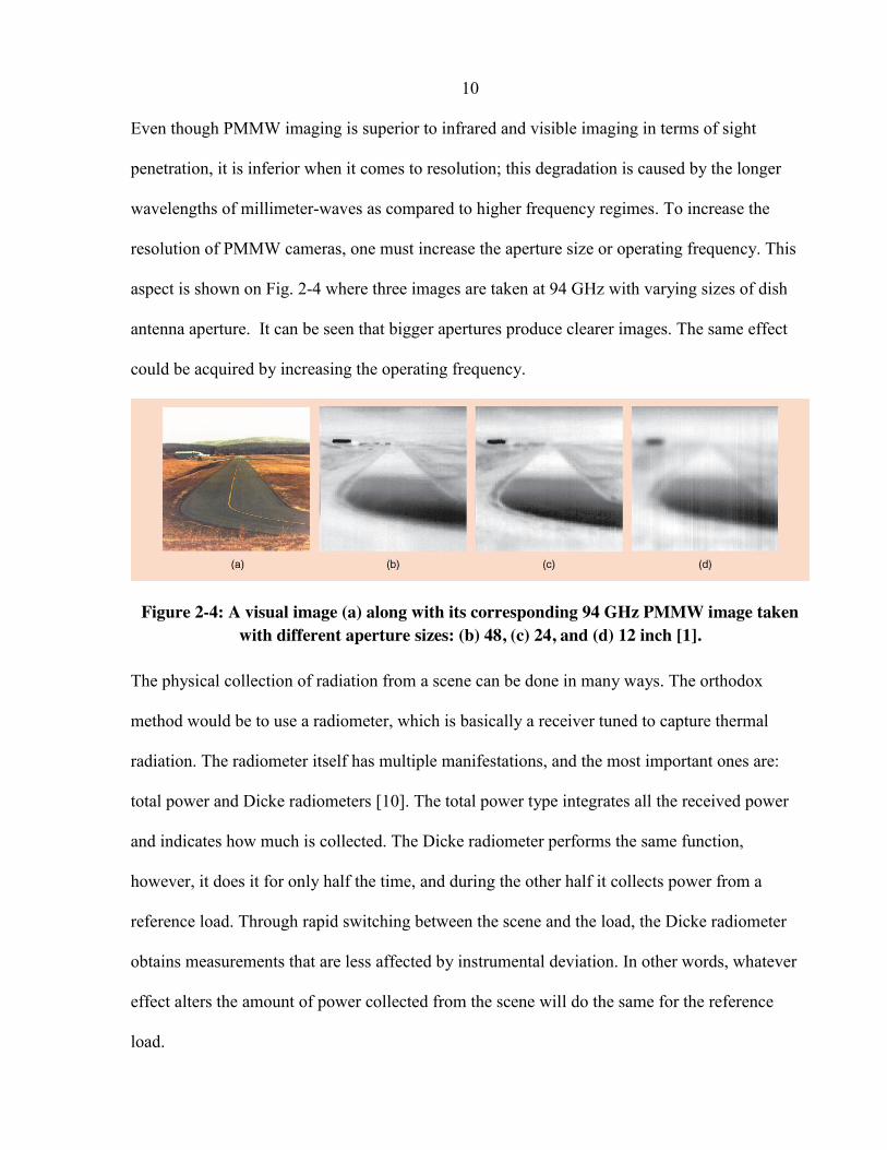
Even though PMMW imaging is superior to infrared and visible imaging in terms of sight
penetration, it is inferior when it comes to resolution; this degradation is caused by the longer
wavelengths of millimeter-waves as compared to higher frequency regimes. To increase the
resolution of PMMW cameras, one must increase the aperture size or operating frequency. This
aspect is shown on Fig. 2-4 where three images are taken at 94 GHz with varying sizes of dish
antenna aperture. It can be seen that bigger apertures produce clearer images. The same effect
could be acquired by increasing the operating frequency.
Figure 2-4: A visual image (a) along with its corresponding 94 GHz PMMW image taken with different aperture sizes: (b) 48, (c) 24, and (d) 12 inch [1].
The physical collection of radiation from a scene can be done in many ways. The orthodox
method would be to use a radiometer, which is basically a receiver tuned to capture thermal
radiation. The radiometer itself has multiple manifestations, and the most important ones are:
total power and Dicke radiometers [10]. The total power type integrates all the received power
and indicates how much is collected. The Dicke radiometer performs the same function,
however, it does it for only half the time, and during the other half it collects power from a
reference load. Through rapid switching between the scene and the load, the Dicke radiometer
obtains measurements that are less affected by instrumental deviation. In other words, whatever
effect alters the amount of power collected from the scene will do the same for the reference
load.

11
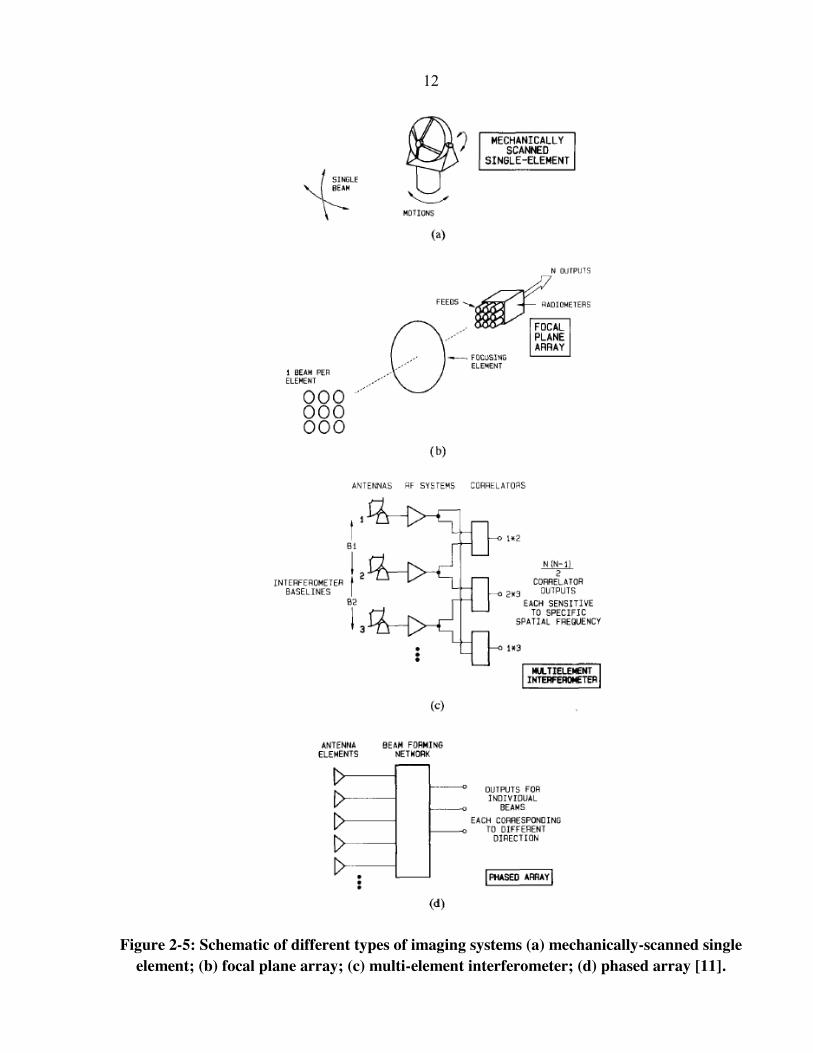
This power collection is done for each pixel in the scene, and moving from one pixel to another
is called scanning. Scanning is typically done using mechanical or electrical means. Mechanical
scanning involves the physical movement of the radiometer, whereas, electrical scanning is
altering the antenna array beam such that its direction of maximum sensitivity changes (phased
array) without actually moving it. A third approach that falls in a different category involves
using a fixed 2D-array (focal plane array) of millimeter-wave receivers; each element in this
array points to one pixel in the scene, thereby collecting power from all pixels. Fig. 2-5 depicts
several configurations of using a radiometer to map a scene.
Using the presented information in this section, one can list the factors that influence the image
produced by a PMMW camera. These factors are summarized in table 2-2.
Table 2-2: Several factors that influence the quality of a PMMW image and their corresponding impact.
Factor Impact Operating frequency
High
Dielectric properties of materials in the scene
High
Radiometer configuration
High
Angle of observation
Medium
Antenna aperture size
Medium
Instrument stability
Medium
Scanning method
Low
Surface roughness of materials in the scene
Low
12
Figure 2-5: Schematic of different types of imaging systems (a) mechanically-scanned single element; (b) focal plane array; (c) multi-element interferometer; (d) phased array [11].

13
2.2 SIW Technology
The metallic rectangular waveguide (RWG) has been used extensively to make microwave
components. Its merits of shielding, high quality factor, and high-frequency compatibility make
it a remarkable transmission line. However, this classic and efficient technology failed to remain
prevalent upon the advent of high-volume circuit production technologies. The bulky nature of
RWG prohibited their substrate integration.
In recent years, researchers invented a scheme to form enclosed metallic waveguides in
conventional substrates using mainstream technologies such as Printed Circuit Board (PCB) [5].
In this scheme (SIW or laminated waveguide), the broad-wall of the waveguide is formed by
metallizing the top and bottom facets of the substrate, and the narrow-wall is synthetically
realized by making a dense array of metallized via-holes which connect both top and bottom
metallized surfaces (Fig. 2-6). This enabled planar integration and mass production of such
waveguides in a low cost manner. In 2011, SIW was listed one of the ten technologies changing
the future of passive and control components by Microwave Journal [12].
Although SIW closely resembles its classical counterpart, it still remains a compromise. Fig. 2-7
features an approximate comparison of the attenuation constant in different transmission lines,
including conventional WG, SIW, and Multilayered SIW. The bulky WG has very low loss, but
it’s not planar, on the other hand, microstrip lines can be integrated, however, they have a
siginificant amount of attenuation. Representing a suitable tradeoff, SIW offers both good
features of integration and low loss.

14
Figure 2-6: SIW and the equivalent RWG [13].
Figure 2-7: A comparison of the attenuation constants of Microstrip line, SIW, Multilayered SIW, and RWG [14].
With its aforementioned merits, SIW enticed researchers in the last decade. Their efforts were
concentrated into making various microwave components using this medium, in order to produce
a compatible system containing one type of transmission line. The creation of this compatible
system would remove lossy transitions going between system constituents. Table 2-3 contains a
variety of microwave components created using the SIW technique or its subsidiaries [15], which

15
proves that SIW can be used as a platform throughout the PMMW imaging system. It can be
seen that all these components operate in the millimeter-wave regime, this makes SIW a suitable
choice for PMMW imaging since it works efficiently in that range of frequencies.
Table 2-3: A variety of microwave SIW components.
Reference Component Description
Design Frequency
Figures of Merit Publish Year
[16]
H-plane T-junction Power
Divider
29.5 GHz
Bandwidth (-19 dB)= 10.2%
Insertion loss= 0.3 – 1 dB
2003
[13] Slot Array Antenna
10 GHz Directivity= 17.4 dB
Gain= 15.7 dB
2004
[17] Degree-2 Circulator
22 GHz Bandwidth (-15 dB)= 18%
Insertion loss= < 1.3 dB
2004
[18]
Multilayered Elliptic Filter
4 GHz
Bandwidth = 140 MHz
Maximum insertion loss
= 0.6 dB
2005
[19]
Six-Port Junction
24 GHz
Bandwidth (-15 dB)= 16.7%
RF ports isolation=
-21 dB
2005
[20]
Single-Balanced
Mixer
10.25 GHz
Conversion
loss= 6.8 dB
< 10 dB conversion
loss bandwidth= 9-
12 GHz
2006
[21]
Rotman Lens
28.5 GHz
Return loss for all ports (28.5 GHz) = < -15
dB
Mutual coupling
between ports (28.5 GHz) =
< -20 dB
2008
[22]
Varactor-Tuned
Phase Shifter
26 GHz
1800 phase shift
bandwidth= 13%
Insertion loss=
3.8 dB
2011
[23]
Magic - T
11 GHz
Bandwidth (-
15 dB) = 49.1%
Amplitude and phase
imbalance = 0.24 dB, 30
2012

16
2.3 LTCC Technology
An obvious solution to reduce a circuit footprint is to form multilayer structures. Ideally, these
layers should be aligned perfectly and fuse to form a monolithic module. Such a description fits
LTCC technology. LTCC is a multilayer ceramic technology where soft ceramic sheets are
independently processed. The processing includes printing conductors, embedding passive
components, or forming cavities. The sheets are then laminated and co-fired at temperatures
below 1000 0C, resulting in a hard monolithic module. The matureness of this technology allows
structures with up to 80 layers to be constructed [24].
A normal LTCC module has several dielectric tapes with external printed conductors and ones
that are buried between the different layers. Resistors and capacitors can be placed inside the
module or on peripheral surfaces, and they manifest as sheets or 3D components. LTCC enables
hybrid integration by adding additional components using typical assembly techniques such as
wire bonding, flip-chip, and soldering. A schematic cross-section of an exemplary LTCC module
is depicted in Fig. 2-8.
Figure 2-8: A schematic cross-section of a model LTCC module [4].
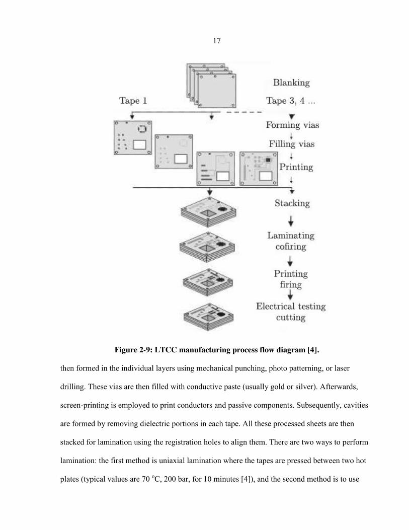
An illustration of the manufacturing process is featured in Fig. 2-9. First of all, the tapes are set
to a standard size, and then registration holes are created for alignment purposes. Via-holes are
17
Figure 2-9: LTCC manufacturing process flow diagram [4].
then formed in the individual layers using mechanical punching, photo patterning, or laser
drilling. These vias are then filled with conductive paste (usually gold or silver). Afterwards,
screen-printing is employed to print conductors and passive components. Subsequently, cavities
are formed by removing dielectric portions in each tape. All these processed sheets are then
stacked for lamination using the registration holes to align them. There are two ways to perform
lamination: the first method is uniaxial lamination where the tapes are pressed between two hot
plates (typical values are 70 oC, 200 bar, for 10 minutes [4]), and the second method is to use

18
isostatic pressure by vacuum packaging the tapes and pressing them in hot water. Finally, the
tapes are co-fired using a specific firing profile and duration depending on the material; in this
step the ceramic solidifies and shrinks in all directions (typical shrinkage values: 12% in x- and
y- directions and 17% in the z-direction [4]). The properties of the LTCC material which will be
used in this work are listed in table 2-4. LTCC technology synergizes with SIW since it offers
3D integration and SIW exploits this aspect by being a shielded transmission line.
Another interesting application of LTCC technology is realizing microsystems [24], this was
enabled by the development of fine line patterning techniques and bonding of LTCC tapes to
other materials.
Table 2-4: DuPont 9K7 GreenTape properties
Property Value Dielectric constant 7.1
Loss tangent 0.001 Breakdown voltage (V/25 m) >1100 Insulation resistance (.cm) >1012
Dimensional thickness – green (m) 127 , 254 Dimensional thickness – fired (m) 112 , 224
Shrinkage x,y (%) 9.1 0.3 Shrinkage z (%) 11.8 0.5
Thermal CTE (ppm/K) 4.4 Thermal conductivity (W/m.K) 4.6
Mechanical density (g/cm3) 3.1 Flexural strength (MPa) 230 Youngs Modulus (GPa) 145
2.4 Integrated SIW Millimeter-Wave Antenna Arrays
For the purposes of listing state-of-the-art, a literature search targeting SIW implementations of
antenna arrays was performed. Under the context of PMMW imaging, these arrays should have

19
large bandwidths and gain. Table 2-5 lists antenna arrays that could potentially be used as
passive front-ends for a PMMW camera. References [20] and [24] fail to be attractive for their
big profile. Although reference [21] presents the smallest size, its bandwidth is narrow, which
reduces the sensitivity of a PMMW imager. Reference [22] has low radiation efficiency and a
relatively big size. Even though reference [23] demonstrated the highest bandwidth, the authors
used a Dielectric Resonator Antenna (DRA), which does not have the same gain throughout the
band of frequencies by virture of being resonant, and this unstability could give rise to issues in
PMMW imaging. To conclude, the current alternatives have quite a number of drawbacks, and
none of them provide an all-round solution. This calls for an investigation to carry their merits
and alleviate their flaws in an innovative design.
Table 2-5: Survey of previous integration of wide-band, high-gain SIW antenna arrays.
Reference
Antenna Type
Design
Frequency
Number of
Antenna Elements
Gain (dBi)
Radiation Efficiency
-10 dB
Bandwidth
Volume
[25] (Fig. 2-10)
Microstrip Patch 12.5 GHz 32 22.5 71% (Measured)
6% > 976 o
[26]
(Fig. 2-11)
Parallel Microstrip
Chain
62 GHz
32
22
74%
(Simulated)
7.6%
135 o
[27]
(Fig. 2-12)
Open-Ended Substrate Integrated Cavities
60 GHz
64
22.1
54.7%
(Simulated)
17.1%
553 o
[28]
(Fig. 2-13)
Dielectric Rod
11 GHz
8
16.5
N/A
31%
502 o
[29]
(Fig. 2-14)
Fermi Tapered Slot Antenna
35 GHz
16
23.4
79%
(N/A)
23.12%
734 o

20
Figure 2-10: Front and backsides of 4 x 8
element PCB-WG-fed array.
Figure 2-11: Photographs of the manufactured LTCC chain array. (a) antenna side, (b) SIW
side.
Figure 2-12: Photograph of the cavity array
antenna on LTCC (left: top view, right: bottom view).
Figure 2-13: Manufactured dielectric rod
antenna array.
Figure 2-14: Photograph of the fabricated 1 x 16 SIW corrugated Fermi-TSA linear array.

21
3 Antenna Array Feeding Network Design
A passive front-end contains two main components, namely, an antenna array, and its
corresponding feeding network. This chapter discusses the feeding network and its sub-
components. After completing the individual components design, it presents their integration to
form the complete feeding network. Finally, electromagnetic simulation results of the complete
feeding network are presented.
However, before delving into the details of the feeding network, the SIW transmission line,
which is the building block of all the discussed components, will be explained, and the
equivalence between the SIW and the classical metallic waveguide will be established. This
serves to shorten the simulation process by using equivalent models.
3.1 SIW Design Consideration
3.1.1 SIW and Its Equivalent Rectangular Waveguide (RWG)
Using a structure that has a dense array of metallic posts in simulators is very time consuming;
since the complexity of the structure requires fine meshing using the Finite Element Method
(FEM). Researchers in the past modeled many waveguide discontinuities using simple circuits
elements [30], which tremendously aided designers in dealing with these discontinuities.
Following the same trend, researchers investigated the similarities between SIW and RWG in
terms of their guided-wave characteristics. A good understanding of this similarity enables the
representation of SIW lines using simple classical waveguides, which significantly cuts down
simulation time.

22
In [31], the generalized admittance matrix of an SIW unit cell was calculated using the BI-RME
(Boundary Integral-Resonant Mode Expansion) method [32]. Using this method, the relation
between the cut-off frequencies of the TE10 and TE20 modes and the SIW line parameters (via-to-
via lateral spacing :W, via diameter :D, and via-to-via pitch :b) was found. Fig. 3-1 depicts this
relationship. Using the least square technique, the cut-off frequency expression for the TE10
mode is approximated from its corresponding curve in Fig. 1.
𝑓 (𝑇𝐸 ) =√
. (𝑊 −.
) (1)
Where c0 is the speed of light in vacuum and r is the substrate relative permittivity.
Examining (1) and mapping it to the cut-off frequency expression for RWG, one can conclude
that SIW can be analyzed as an equivalent rectangular waveguide with the following effective
width (with the condition that via-to-via pitch is sufficiently small):
𝑊 = 𝑊 −.
(2)
To verify these empirical equations, an SIW and its equivalent RWG were simulated in [31].
Afterwards, their propagation constants were extracted to plot and compare their dispersion
curves. As seen in Fig. 3-2, both guides have the same propagation constant, and thereby exhibit
a matching dispersion characteristic, which validates the proposed equations in [31].
3.1.2 Choosing SIW Line Parameters
In order to establish useful design rules, researchers in [33] analyzed SIW to determine its
complex propagation constant. In [33], fundamental guided waves and leakage properties were
demonstrated for this structure. When choosing SIW line parameters, one must consider two
aspects, namely, leakage losses and bandgap effects.

23
Figure 3-1: Cut-off frequencies of the TE10-like and TE20-like modes of the straight pattern SIW versus W and D [31].
Figure 3-2: Comparison of the dispersion curves of an SIW with an equivalent rectangular waveguide [31].
When the via-to-via pitch is no longer sufficiently small, the fields cease to be completely
confined between the two rows of vias. This loss manifests as coupling between the TE10 mode
24
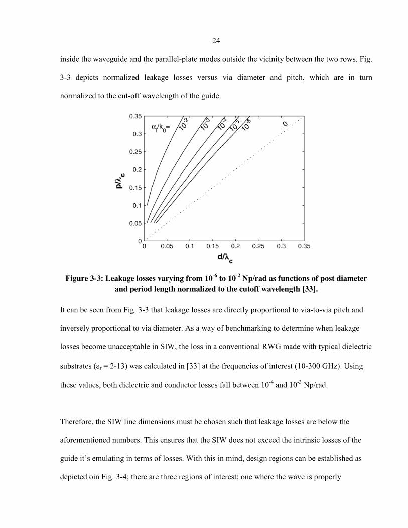
inside the waveguide and the parallel-plate modes outside the vicinity between the two rows. Fig.
3-3 depicts normalized leakage losses versus via diameter and pitch, which are in turn
normalized to the cut-off wavelength of the guide.
Figure 3-3: Leakage losses varying from 10-6 to 10-2 Np/rad as functions of post diameter and period length normalized to the cutoff wavelength [33].
It can be seen from Fig. 3-3 that leakage losses are directly proportional to via-to-via pitch and
inversely proportional to via diameter. As a way of benchmarking to determine when leakage
losses become unacceptable in SIW, the loss in a conventional RWG made with typical dielectric
substrates (r = 2-13) was calculated in [33] at the frequencies of interest (10-300 GHz). Using
these values, both dielectric and conductor losses fall between 10-4 and 10-3 Np/rad.
Therefore, the SIW line dimensions must be chosen such that leakage losses are below the
aforementioned numbers. This ensures that the SIW does not exceed the intrinsic losses of the
guide it’s emulating in terms of losses. With this in mind, design regions can be established as
depicted oin Fig. 3-4; there are three regions of interest: one where the wave is properly
25
confined, making it suitable for passive components, and other where the wave is leaking outside
the structure, rendering it suitable for antennas. The third region must be avoided as it fails to
satisfy both previous options.
Figure 3-4: Guided-wave region, leaky-wave region, and wave-forbidden region in the plane of d/c, p/c [33].
Electromagnetic bandgap phenomenon can occur in periodic structures, thus, designers must
ensure that this occurrence does not fall in the operation bandwidth. This phenomenon introduces
a transmission zero at the frequency of resonance, at which, the via-to-via pitch will represent a
half-wavelength separation. Since each via is reactive, this specific separation will cause the
addition of these reactances, and ultimately render the input impedance tremendously reactive.
This will reflect the impinging wave and cease its transmission. In [33], a more restrictive
condition is made to avoid bandgap effects in the bandwidth of operation. This condition permits
the via-to-via separation to be less than one-fourth of the cutoff wavelength (p/c =0.25). Finally,
one more effect to consider is the minimization of the number of vias such that the mechanical
26
rigidity of the substrate is not affected. With all the aforementioned aspects in mind, Fig. 3-5
shows an interesting region for realizing SIW circuitry.
Figure 3-5: Region of interest for the SIW in the plane of d/c, p/c [33].
In this work, DuPont 9K7 substrate is used, thus, the pitch and diameter were chosen such that
they provide the least amount of losses without violating design rules. The LTCC fabrication
foundry could only realize a via diameter of 0.14 mm, due to limitations of the punching
machine. The via-to-via pitch was chosen to be 0.375 mm as per the foundry’s minimum
acceptable spacing.
3.2 Beamforming Network Design Considerations
The radiation pattern of a single antenna element is typically not directive, which is why for
applications that require high-gain, an array of antenna elements is configured to produce a
narrower beam. The gain enhancement is a result of the constructive interference of the
individual antenna beams in a targeted direction. Although not necessary, the elements of an

27
array are usually identical for simplicity and design practicality. There are five factors that
influence the radiation pattern shape of such an array [34]:
1. Geometrical array configuration (linear, planar, circular, etc).
2. Element-to-element spacing.
3. Relative excitation amplitude of each element.
4. Relative excitation phase of each element.
5. Radiation pattern of the individual antenna element.
It can be seen that two out of the five factors (3 and 4) are solely based on the array feeding
network. In other words, the feeding network design plays an essential role in determining the
beam’s shape. There are three main aspects to consider when making a feeding network, namely,
(1) the network efficiency, (2) the phase excitation of each element, and (3) the excitation
amplitude coefficients.
The network efficiency depends on the leakage and dissipation exhibited by the components
employed in the design. To ensure that the maximum gain direction does not deviate from the
center of the array, all elements must have an equi-phase excitation, which is done by ensuring
the wave traverses the same distance in all different paths. Finally, the aspect which is not
straightforward to design is the relative amount of field intensity or power delivered to each
antenna element.
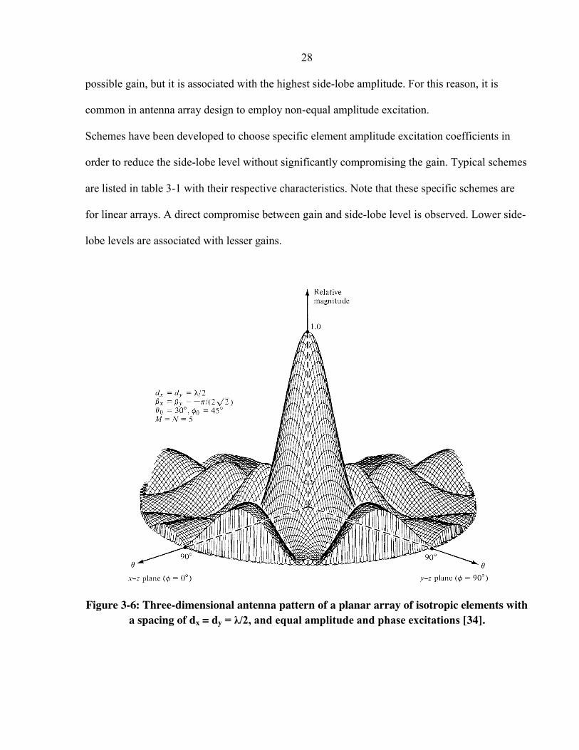
Fig. 3-6 shows a 3D radiation pattern of an array with isotropic elements and equal amplitude
and phase excitation. The “bumps” that are observed around the z-axis in Fig. 3-6 are called side-
lobes. Their existence causes the array to receive unwanted radiation from untargeted pixels for a
PMMW system. Practically, side-lobes cannot be completely eliminated, however, their
amplitude can be reduced. Exciting the elements with equal amplitude results in the highest
28
possible gain, but it is associated with the highest side-lobe amplitude. For this reason, it is
common in antenna array design to employ non-equal amplitude excitation.
Schemes have been developed to choose specific element amplitude excitation coefficients in
order to reduce the side-lobe level without significantly compromising the gain. Typical schemes
are listed in table 3-1 with their respective characteristics. Note that these specific schemes are
for linear arrays. A direct compromise between gain and side-lobe level is observed. Lower side-
lobe levels are associated with lesser gains.
Figure 3-6: Three-dimensional antenna pattern of a planar array of isotropic elements with a spacing of dx = dy = λ/2, and equal amplitude and phase excitations [34].

29
Table 3-1: Schemes for linear antenna array radiation pattern synthesis using non-equal amplitude excitation [35].
3.3 Feeding Network Components
A feeding network is comprised of mainly three components, (1) one-to-two power splitter is
typically used, and the power division could either be equal or arbitrary depending on the
network type and the division stage. (2) traversing from one power division block to another
requires moving in two dimensions, which mandates the presence of H-plane bends. (3) a
transition may be employed to connect the feeding network to external circuitry for testing
30
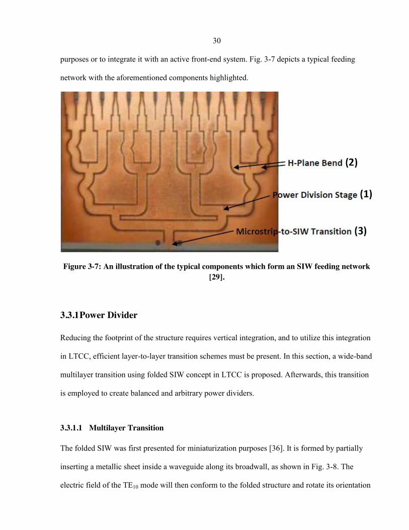
purposes or to integrate it with an active front-end system. Fig. 3-7 depicts a typical feeding
network with the aforementioned components highlighted.
Figure 3-7: An illustration of the typical components which form an SIW feeding network [29].
3.3.1 Power Divider
Reducing the footprint of the structure requires vertical integration, and to utilize this integration
in LTCC, efficient layer-to-layer transition schemes must be present. In this section, a wide-band
multilayer transition using folded SIW concept in LTCC is proposed. Afterwards, this transition
is employed to create balanced and arbitrary power dividers.
3.3.1.1 Multilayer Transition
The folded SIW was first presented for miniaturization purposes [36]. It is formed by partially
inserting a metallic sheet inside a waveguide along its broadwall, as shown in Fig. 3-8. The
electric field of the TE10 mode will then conform to the folded structure and rotate its orientation

31
accordingly. At frequencies where the full width of the folded structure satisfies the cut-off
frequency requirement, the structure exhibits interesting characteristics; the maximum value of
the electric field occurs at the small gap between the end of the inserted plate and the narrow
wall of the structure, thereby resembling the distribution magnitude found in the conventional
waveguide (i.e. maximum field value occurring at the width’s center). However, when
considering the vicinities above and below the inserted plate to be separate waveguides of full
width, at such a frequency, this structure forms a multilayer transition through a coupling slot in
the common broadwall.
Figure 3-8: Geometry of (a) SIW and (b) Folded SIW.
Fig. 3-9 shows the proposed structure of the multilayer transition. Two waveguides lying on
different layers are connected through a longitudinal slot, and the slot is positioned at the
extreme side of the broadwall. The upper waveguide is gradually terminated as the slot opens,
whereas, the lower waveguide gradually opens to eventually reach full width as the slot
terminates. The optimization of this structure is fairly easy with one parameter to choose,
namely, the length of the slot Ls. The multilayer transition has been optimized for the frequency
band from 32 GHz to 38 GHz, and its geometrical dimensions are listed in Fig. 3-9.
32
Figure 3-9: Geometry of the multilayer transition: Ls = 9.16mm, Ws =0.105mm, Wt = 2mm and Wsiw= 2.39mm, P=0.375mm and d=0.1363mm.
The fired layer thickness used in the model is 0.112 mm, and the substrate material is DuPont
9K7 with a dielectric constant of 7.1 and a loss tangent of 0.001. The electric field magnitude
inside the structure, represented in cross sections, is shown in Fig. 3-10. At first (a), the fields
totally reside within the upper waveguide, and as it terminates ((b)-(d)), the field transfers to the
lower waveguide (red color represents large magnitudes) and eventually resides completely
inside it (e).
Figure 3-10: Multilayer transition E-field magnitude distribution simulated at 35GHz for different cross-sections.
33
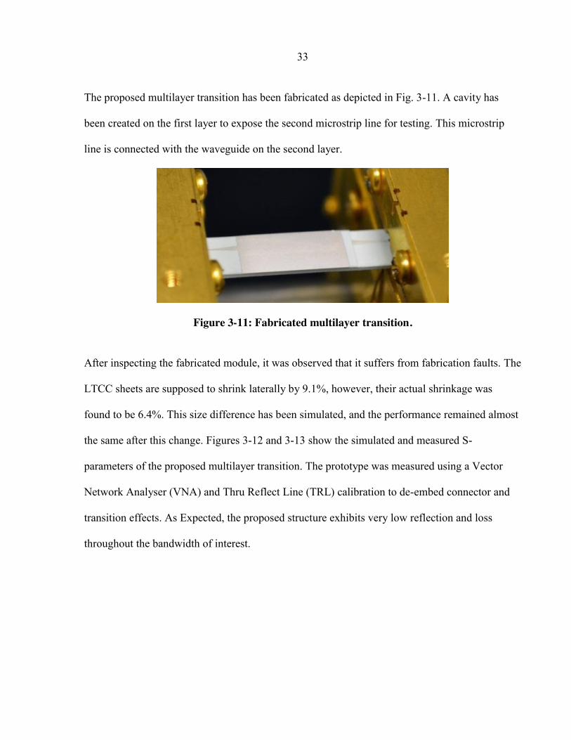
The proposed multilayer transition has been fabricated as depicted in Fig. 3-11. A cavity has
been created on the first layer to expose the second microstrip line for testing. This microstrip
line is connected with the waveguide on the second layer.
Figure 3-11: Fabricated multilayer transition.
After inspecting the fabricated module, it was observed that it suffers from fabrication faults. The
LTCC sheets are supposed to shrink laterally by 9.1%, however, their actual shrinkage was
found to be 6.4%. This size difference has been simulated, and the performance remained almost
the same after this change. Figures 3-12 and 3-13 show the simulated and measured S-
parameters of the proposed multilayer transition. The prototype was measured using a Vector
Network Analyser (VNA) and Thru Reflect Line (TRL) calibration to de-embed connector and
transition effects. As Expected, the proposed structure exhibits very low reflection and loss
throughout the bandwidth of interest.
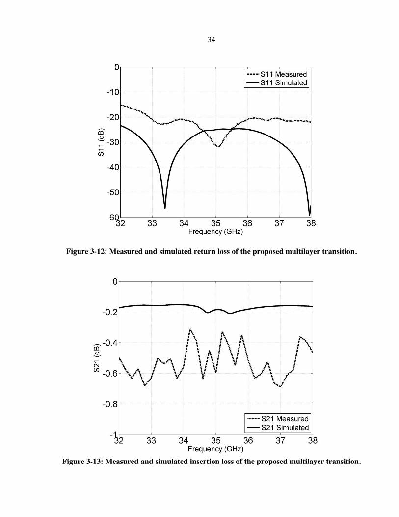
34
Figure 3-12: Measured and simulated return loss of the proposed multilayer transition.
Figure 3-13: Measured and simulated insertion loss of the proposed multilayer transition.
35
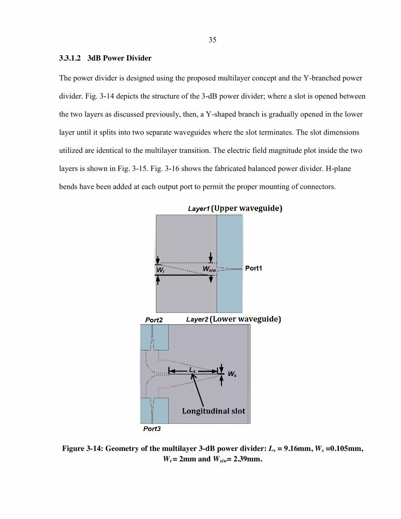
3.3.1.2 3dB Power Divider
The power divider is designed using the proposed multilayer concept and the Y-branched power
divider. Fig. 3-14 depicts the structure of the 3-dB power divider; where a slot is opened between
the two layers as discussed previously, then, a Y-shaped branch is gradually opened in the lower
layer until it splits into two separate waveguides where the slot terminates. The slot dimensions
utilized are identical to the multilayer transition. The electric field magnitude plot inside the two
layers is shown in Fig. 3-15. Fig. 3-16 shows the fabricated balanced power divider. H-plane
bends have been added at each output port to permit the proper mounting of connectors.
Figure 3-14: Geometry of the multilayer 3-dB power divider: Ls = 9.16mm, Ws =0.105mm, Wt = 2mm and Wsiw= 2.39mm.
36
Figure 3-15: Balanced power divider E-field magnitude distribution simulated at 35GHz.
Figure 3-16: Fabricated multilayer balanced power divider.
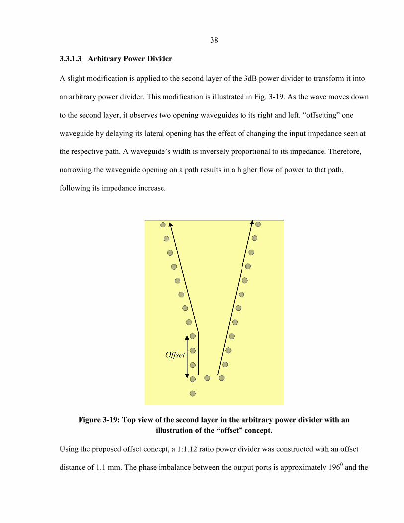
The simulated and measured S-parameters of the balanced power divider are depicted on figures
3-17 and 3-18. A good agreement is observed between simulation and measurement of the return
loss. Although the measured transmission parameters exhibit more losses compared to
simulation, the proposed 3dB power divider separates the input power with equal proportions.
This additional loss could be contributed to the fabrication imperfections, which might have
resulted in a deformed microstrip line. Also, the irregular measurement setup, which involves
two layers, could be another contributor to the observed loss. The phase shift between the two
output ports is 1820 ± 0.70 in the bandwidth of interest.
37
Figure 3-17: Measured and simulated return loss of the proposed multilayer 3dB power divider.
Figure 3-18: Measured and simulated transmission parameters of the proposed multilayer 3dB power divider.
38
3.3.1.3 Arbitrary Power Divider
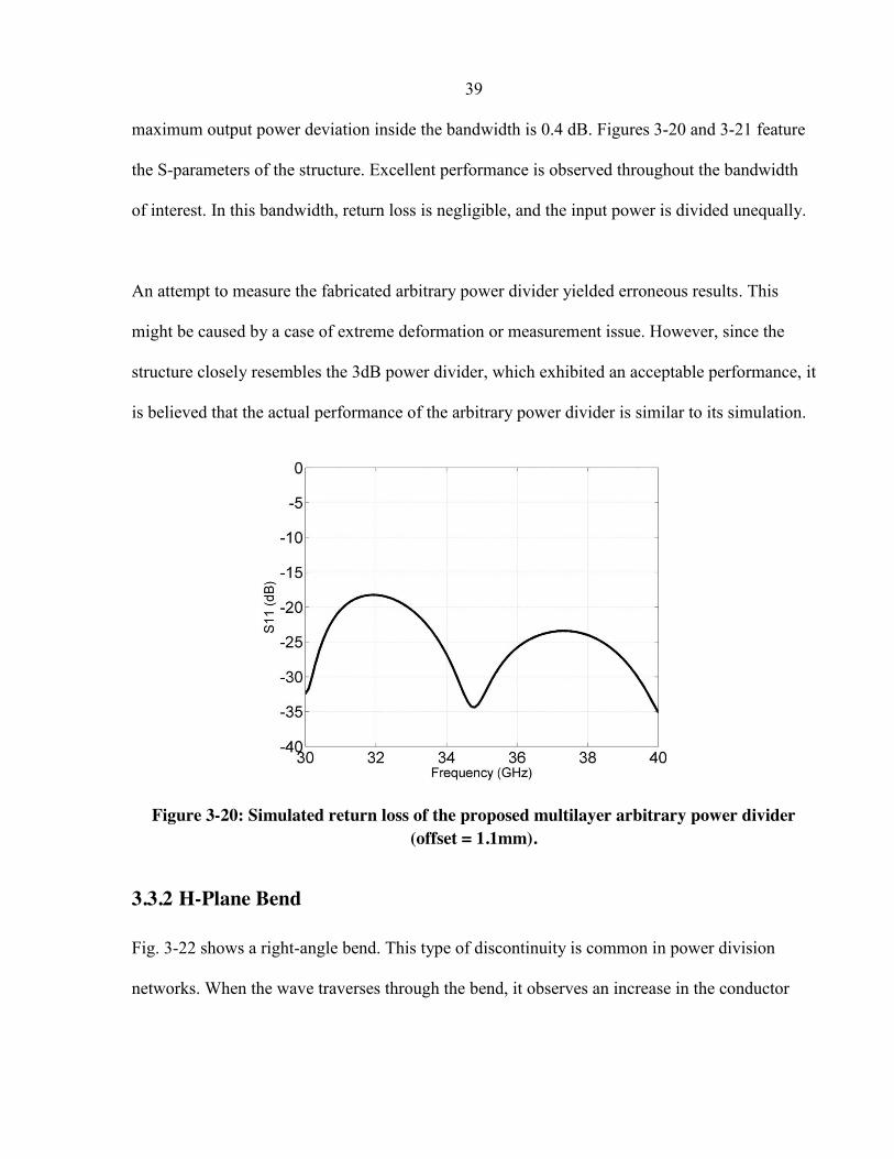
A slight modification is applied to the second layer of the 3dB power divider to transform it into
an arbitrary power divider. This modification is illustrated in Fig. 3-19. As the wave moves down
to the second layer, it observes two opening waveguides to its right and left. “offsetting” one
waveguide by delaying its lateral opening has the effect of changing the input impedance seen at
the respective path. A waveguide’s width is inversely proportional to its impedance. Therefore,
narrowing the waveguide opening on a path results in a higher flow of power to that path,
following its impedance increase.
Figure 3-19: Top view of the second layer in the arbitrary power divider with an illustration of the “offset” concept.
Using the proposed offset concept, a 1:1.12 ratio power divider was constructed with an offset
distance of 1.1 mm. The phase imbalance between the output ports is approximately 1960 and the
39
maximum output power deviation inside the bandwidth is 0.4 dB. Figures 3-20 and 3-21 feature
the S-parameters of the structure. Excellent performance is observed throughout the bandwidth
of interest. In this bandwidth, return loss is negligible, and the input power is divided unequally.
An attempt to measure the fabricated arbitrary power divider yielded erroneous results. This
might be caused by a case of extreme deformation or measurement issue. However, since the
structure closely resembles the 3dB power divider, which exhibited an acceptable performance, it
is believed that the actual performance of the arbitrary power divider is similar to its simulation.
Figure 3-20: Simulated return loss of the proposed multilayer arbitrary power divider (offset = 1.1mm).
3.3.2 H-Plane Bend
Fig. 3-22 shows a right-angle bend. This type of discontinuity is common in power division
networks. When the wave traverses through the bend, it observes an increase in the conductor
40
area, which in turn increases the capacitance at that point. The presence of this reactance causes a
mismatch at the turn junction and results in return loss.
Figure 3-21: Simulated insertion loss of the proposed multilayer arbitrary power divider (offset = 1.1 mm).
Figure 3-22: Top view of a waveguide right-angle bend.

41
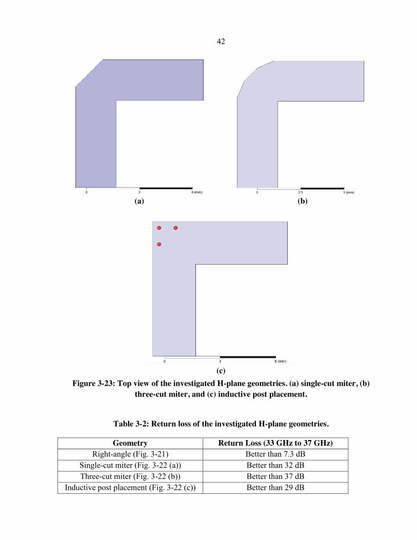
Several techniques were established to alleviate the return loss issue. Typical desirable values for
the return loss would be below -35 dB. Three prevalent geometries were investigated as
candidate solutions. They are shown in Fig. 3-23. The first technique miters the corner to reduce
the excess capacitance (Fig. 3-23 (a)). However, the increase in conductor area varies along the
junction, and thus, one miter cut is an approximation. For this reason, a further modification
exists, which uses three symmetrical cuts to miter the corner (Fig. 3-23 (b)), thereby accounting
for the capacitance variance property. Finally, a third technique introduces inductive posts at the
discontinuity to compensate for the negative reactance part (Fig. 3-23 (c)).
To choose one of these techniques, the three geometries were simulated using the DuPont 9K7
substrate and the SIW line parameters achieved earlier. The return loss value, for each geometry
across the desired bandwidth, is listed in table 3-2. An equivalent RWG was employed to
simulate all structures.
It can be seen from table 3-2 that the three-cut miter geometry presents fewer losses than its
alternatives, and thus, it will be implemented using via-holes to ultimately incorporate it in the
feeding network. Fig. 3-24 depicts the via-hole implementation of the three-cut miter geometry.
The vias around the corner are not spaced uniformly, this is to form the specific length of miter
corner. Figures 3-25 and 3-26 show the simulated S-parameters of the structure. The port-to-port
distance in the simulation setup is 14.6 mm. As expected from the accuracy of the equivalent
RWG model, the simulation results demonstrate excellent performance.
42
(a)
(b)
(c)
Figure 3-23: Top view of the investigated H-plane geometries. (a) single-cut miter, (b) three-cut miter, and (c) inductive post placement.
Table 3-2: Return loss of the investigated H-plane geometries.
Geometry Return Loss (33 GHz to 37 GHz) Right-angle (Fig. 3-21) Better than 7.3 dB
Single-cut miter (Fig. 3-22 (a)) Better than 32 dB Three-cut miter (Fig. 3-22 (b)) Better than 37 dB
Inductive post placement (Fig. 3-22 (c)) Better than 29 dB

43
Figure 3-24: Top view of the via-hole implementation of the three-cut miter H-plane bend.
Figure 3-25: Simulated return loss of the SIW three-cut miter H-plane bend.

44
Figure 3-26: Simulated insertion loss of the SIW three-cut miter H-plane bend.
Although the SIW H-plane has been fabricated, it could not be tested. This is because the two
ports of the fabricated module are too close to allow proper connector mounting. However, this
component is used extensively in the complete feeding network, which demonstrates a good
performance as will be discussed later. For this reason, it can be inferred that the SIW H-plane
bend is working properly.
3.3.3 Microstrip-to-SIW Transition
To connect SIW to active or external circuitry, a transition is usually needed. The choice of
microstrip stems from its prevalence and compatibility with most microwave circuitry. Also, a
wide-band microstrip-to-SIW transition exists [5], and the performance of this transition is equal
or superior to other transitions at millimeter-waves.
Fig. 3-27 shows the geometry of the transition. The transition serves two purposes, namely, to
transform the field orientation in the microstrip line to the field inside the waveguide (Fig. 3-28),
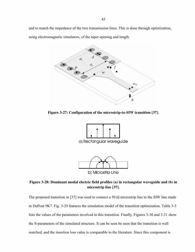
45
and to match the impedance of the two transmission lines. This is done through optimization,
using electromagnetic simulators, of the taper opening and length.
Figure 3-27: Configuration of the microstrip-to-SIW transition [37].
Figure 3-28: Dominant modal electric field profiles (a) in rectangular waveguide and (b) in microstrip line [37].
The proposed transition in [37] was used to connect a 50 Ω microstrip line to the SIW line made
in DuPont 9K7. Fig. 3-29 features the simulation model of the transition optimization. Table 3-3
lists the values of the parameters involved in this transition. Finally, Figures 3-30 and 3-31 show
the S-parameters of the simulated structure. It can be seen be seen that the transition is well
matched, and the insertion loss value is comparable to the literature. Since this component is
46
inherently present in all fabricated components for accessibility, simply being able to measure
them implies that this part works.
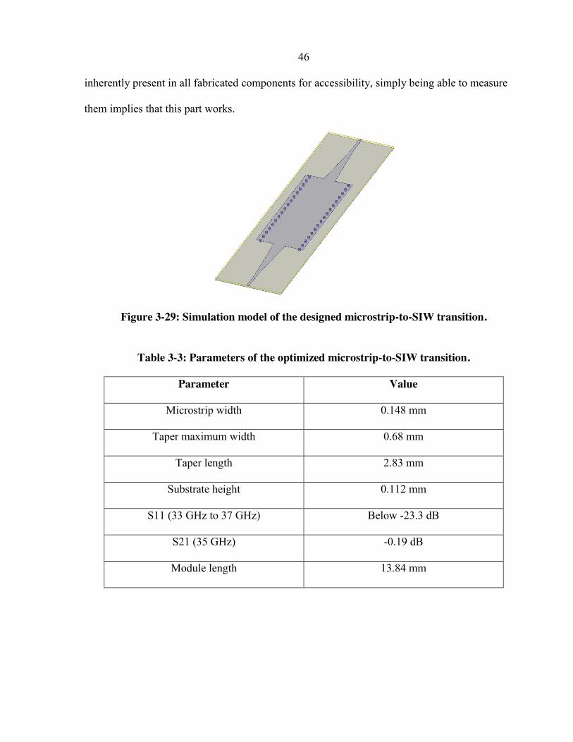
Figure 3-29: Simulation model of the designed microstrip-to-SIW transition.
Table 3-3: Parameters of the optimized microstrip-to-SIW transition.
Parameter Value
Microstrip width 0.148 mm
Taper maximum width 0.68 mm
Taper length 2.83 mm
Substrate height 0.112 mm
S11 (33 GHz to 37 GHz) Below -23.3 dB
S21 (35 GHz) -0.19 dB
Module length 13.84 mm

47
Figure 3-30: Return loss of the optimized microstrip-to-SIW transition.
Figure 3-31: Insertion loss of the optimized microstrip-to-SIW transition.

48
After designing all the required components, the next step is to integrate them to create the
network.
3.4 Feeding Network Architecture
The main choice that influences the network architecture is the non-equal amplitude coefficient
scheme. The chosen scheme has to satisfy the system side-lobe level requirement, which is in our
case for the maximum side-lobe level to be less than -15 dB. It also has to be realizable with the
designed components.
For the purposes of this work, the quasi-triangular power distribution will be used. This scheme
solely uses identical power divider stages to taper the amplitude distribution in a linear manner.
It satisfies the system requirements by having a theoretical side-lobe level of approximately 20
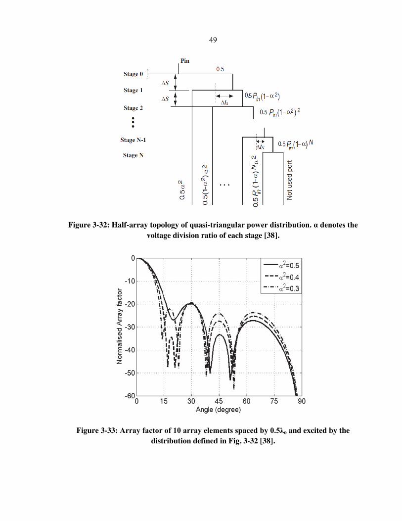
dB, and it can be realized using the proposed 3dB power divider. Fig. 3-32 shows a half-array
with quasi-triangular distribution. A cascade of identical power dividers is used where one output
port in each division stage is directly fed to its respective antenna element. Using 3dB power
dividers renders the power difference between each consecutive ports 3dB. Note that the outer
port in this architecture is not used to properly realize the distribution.
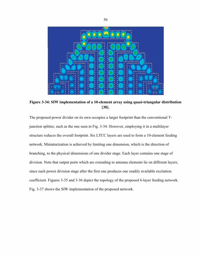
Fig. 3-33 depicts the array factor of 10-elements with half-wavelength spacing for different
values of α. Fig. 3-34 shows an SIW implementation of a 10-element feeding network with its E-
field magnitude distribution.
In this work, the distribution in Fig. 3-32 is modified by adding a variable power divider for the
last stage. This achieves almost the same side-lobe level without having to forfeit the power in
the outer port.
49
Figure 3-32: Half-array topology of quasi-triangular power distribution. α denotes the voltage division ratio of each stage [38].
Figure 3-33: Array factor of 10 array elements spaced by 0.5λo and excited by the distribution defined in Fig. 3-32 [38].
50
Figure 3-34: SIW implementation of a 10-element array using quasi-triangular distribution [38].
The proposed power divider on its own occupies a larger footprint than the conventional T-
junction splitter, such as the one seen in Fig. 3-34. However, employing it in a multilayer
structure reduces the overall footprint. Six LTCC layers are used to form a 10-element feeding
network. Miniaturization is achieved by limiting one dimension, which is the direction of
branching, to the physical dimensions of one divider stage. Each layer contains one stage of
division. Note that output ports which are extending to antenna elements lie on different layers,
since each power division stage after the first one produces one readily available excitation
coefficient. Figures 3-35 and 3-36 depict the topology of the proposed 6-layer feeding network.
Fig. 3-37 shows the SIW implementation of the proposed network.
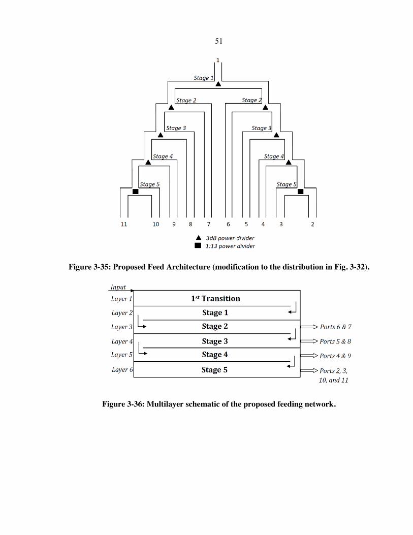
51
Figure 3-35: Proposed Feed Architecture (modification to the distribution in Fig. 3-32).
Figure 3-36: Multilayer schematic of the proposed feeding network.

52
Figure 3-37: Implementation of the proposed feeding network. The intermittent blue boxes
illustrate the interaction between the different layers.
3.5 Feeding Network Simulation Results
The proposed feeding network has been simulated to extract its performance. To shorten
simulation time, and since the structure is symmetric, only half the network is simulated. Fig. 3-
38 depicts the used simulation model. Fig. 3-39 shows the transmission parameters at each of the
five output ports, and a general stability is observed throughout a significant frequency band.
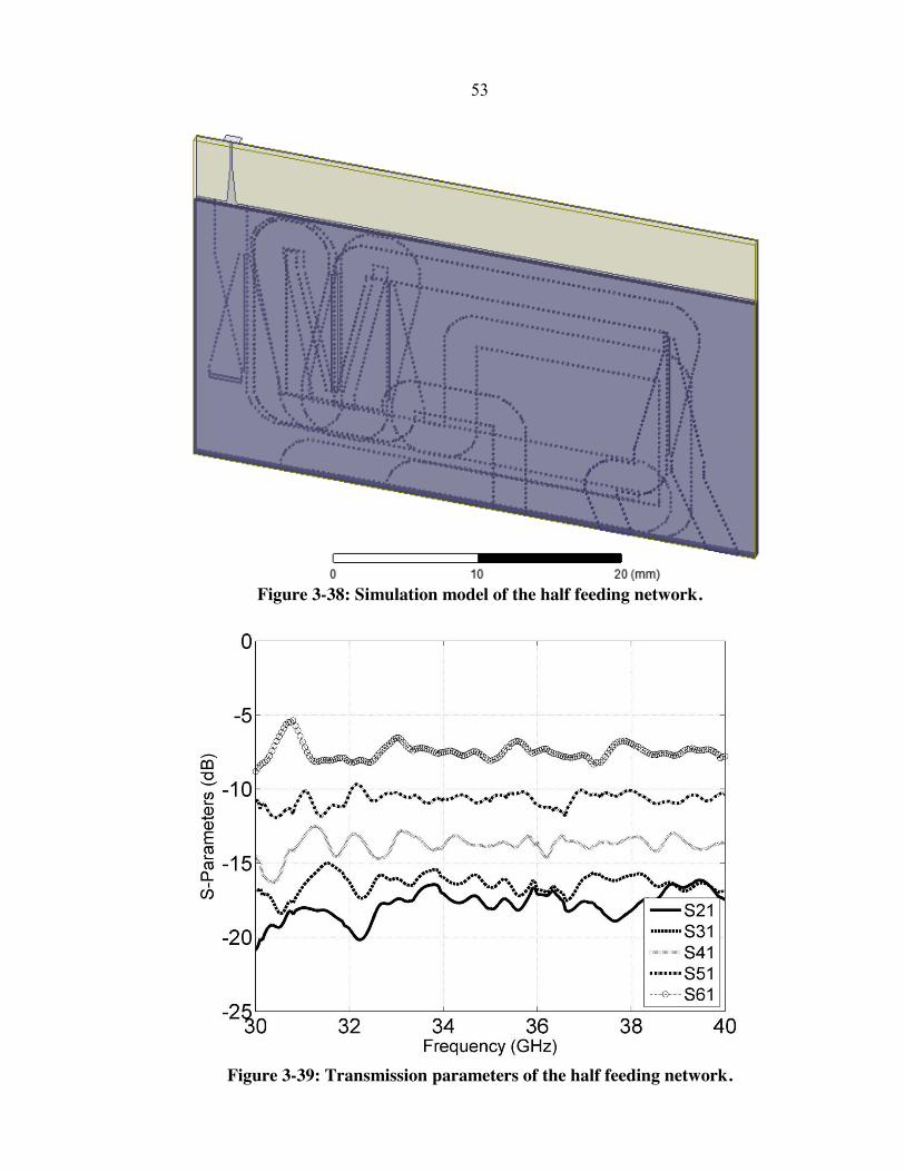
53
Figure 3-38: Simulation model of the half feeding network.
Figure 3-39: Transmission parameters of the half feeding network.

54
Another aspect which must be investigated is the phase excitation at each port. For this purpose,
Fig. 3-40 features the phase difference between the output ports, which ideally should be zero. It
can be seen that the phase difference goes to zero at 35 GHz, and remains low within the
bandwidth of interest. In other words, the maximum gain direction of the beam, within the
specified frequency band, does not deviate.
Figure 3-40: Phase difference between the output ports of the half feeding network.
Knowing the S-parameters, one can find two things, namely, (1) the amplitude excitation
coefficients, and thus the expected beam shape, and (2) the network efficiency. Table 3-4 lists
the amplitude excitations coefficient at each port in the complete feeding network. Fig. 3-41
shows a 10-element array factor plot using these coefficients. The element-to-element spacing is
set to 0.92 λo to conform to the dimensions of the designed antenna, which will be discussed in
Chapter 4. The achieved maximum side-lobe level is approximately 20 dB, which is expected
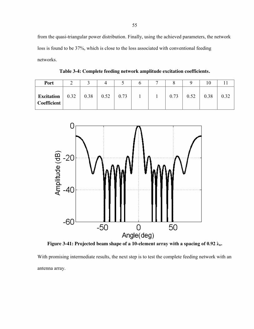
55
from the quasi-triangular power distribution. Finally, using the achieved parameters, the network
loss is found to be 37%, which is close to the loss associated with conventional feeding
networks.
Table 3-4: Complete feeding network amplitude excitation coefficients.
Port 2 3 4 5 6 7 8 9 10 11
Excitation Coefficient
0.32
0.38
0.52
0.73
1
1
0.73
0.52
0.38
0.32
Figure 3-41: Projected beam shape of a 10-element array with a spacing of 0.92 λo.
With promising intermediate results, the next step is to test the complete feeding network with an
antenna array.

56
4 Antenna Integration
Upon completion of the feeding network, the next step to realize the passive front-end is to
integrate the antenna array. It was intended to make a monolithic front-end on LTCC by using
the same medium for the feeding network and the antenna .Several attempted LTCC antenna
designs were attempted, however, these designs either could not meet all PMMW camera
requirements (mainly due to the high permittivity of LTCC) or were unsuitable for LTCC
implementation. Nonetheless, these designs are presented in this chapter. For feed network
characterization, an antenna design has been carried on a lower permittivity substrate, namely,
Rogers, to alleviate the abovementioned issues. Afterwards, the two substrates (LTCC and
Rogers) are integrated using efficient transitions. Finally, the results of the complete structure are
outlined and discussed.
4.1 LTCC Antenna
For our particular application, the requirements are for the passive front-end to provide a gain of
at least 20 dBi and a bandwidth of more than 4 GHz. It should also operate at 35 GHz. In this
section, the attempted antenna designs on LTCC are presented. The performance of each antenna
is discussed, and the reasons for their unsuitability are mentioned.
Since the feeding network is implemented in SIW technology, a horn antenna, which can be
implemented using SIW, is a very suitable choice. The compatibility between an antenn and its
feed, removes the need of complex and lossy transitions.
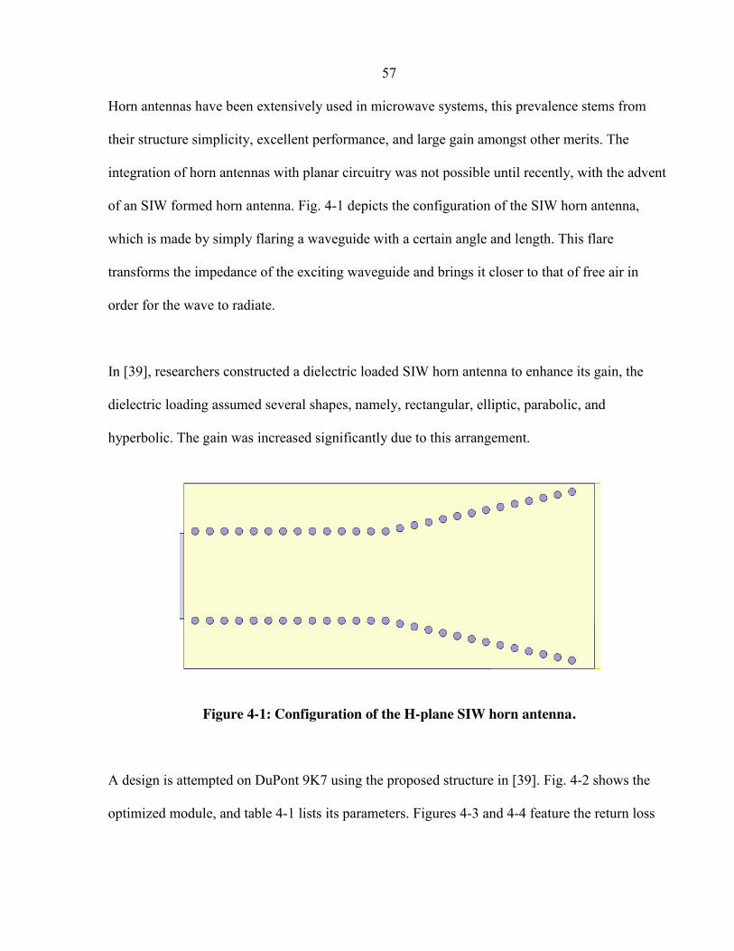
57
Horn antennas have been extensively used in microwave systems, this prevalence stems from
their structure simplicity, excellent performance, and large gain amongst other merits. The
integration of horn antennas with planar circuitry was not possible until recently, with the advent
of an SIW formed horn antenna. Fig. 4-1 depicts the configuration of the SIW horn antenna,
which is made by simply flaring a waveguide with a certain angle and length. This flare
transforms the impedance of the exciting waveguide and brings it closer to that of free air in
order for the wave to radiate.
In [39], researchers constructed a dielectric loaded SIW horn antenna to enhance its gain, the
dielectric loading assumed several shapes, namely, rectangular, elliptic, parabolic, and
hyperbolic. The gain was increased significantly due to this arrangement.
Figure 4-1: Configuration of the H-plane SIW horn antenna.
A design is attempted on DuPont 9K7 using the proposed structure in [39]. Fig. 4-2 shows the
optimized module, and table 4-1 lists its parameters. Figures 4-3 and 4-4 feature the return loss
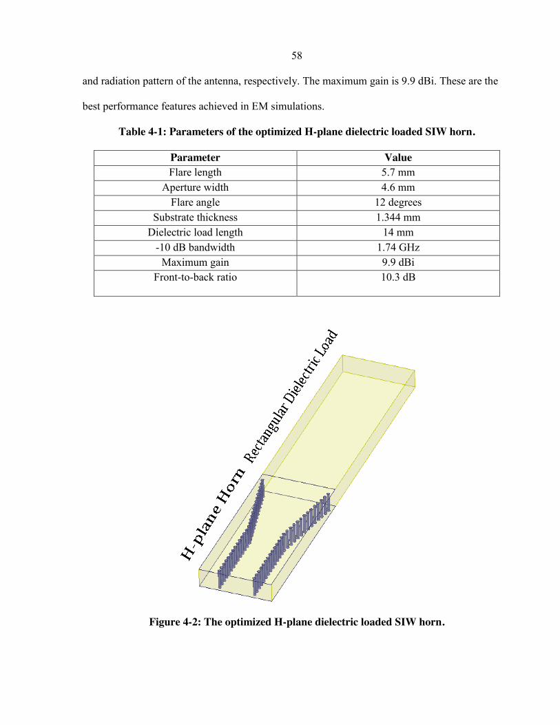
58
and radiation pattern of the antenna, respectively. The maximum gain is 9.9 dBi. These are the
best performance features achieved in EM simulations.
Table 4-1: Parameters of the optimized H-plane dielectric loaded SIW horn.
Parameter Value Flare length 5.7 mm
Aperture width 4.6 mm Flare angle 12 degrees
Substrate thickness 1.344 mm Dielectric load length 14 mm
-10 dB bandwidth 1.74 GHz Maximum gain 9.9 dBi
Front-to-back ratio 10.3 dB
Figure 4-2: The optimized H-plane dielectric loaded SIW horn.
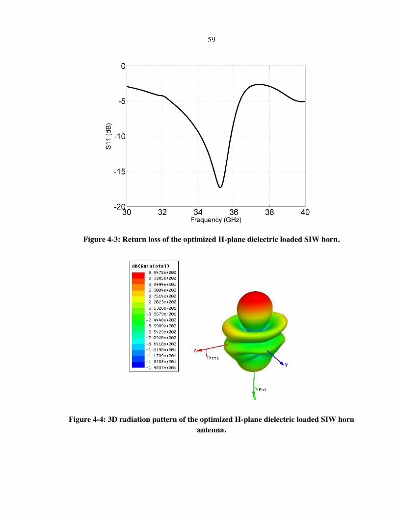
59
Figure 4-3: Return loss of the optimized H-plane dielectric loaded SIW horn.
Figure 4-4: 3D radiation pattern of the optimized H-plane dielectric loaded SIW horn antenna.
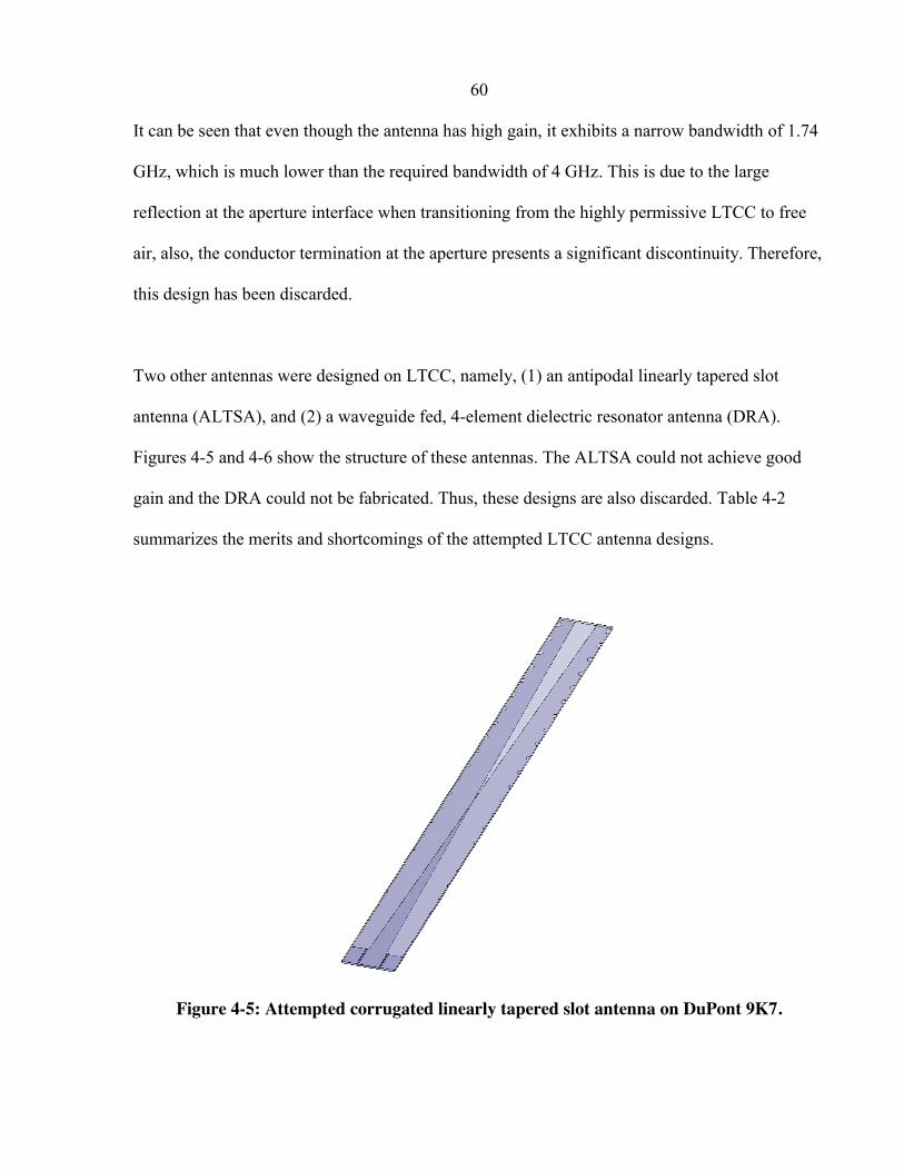
60
It can be seen that even though the antenna has high gain, it exhibits a narrow bandwidth of 1.74
GHz, which is much lower than the required bandwidth of 4 GHz. This is due to the large
reflection at the aperture interface when transitioning from the highly permissive LTCC to free
air, also, the conductor termination at the aperture presents a significant discontinuity. Therefore,
this design has been discarded.
Two other antennas were designed on LTCC, namely, (1) an antipodal linearly tapered slot
antenna (ALTSA), and (2) a waveguide fed, 4-element dielectric resonator antenna (DRA).
Figures 4-5 and 4-6 show the structure of these antennas. The ALTSA could not achieve good
gain and the DRA could not be fabricated. Thus, these designs are also discarded. Table 4-2
summarizes the merits and shortcomings of the attempted LTCC antenna designs.
Figure 4-5: Attempted corrugated linearly tapered slot antenna on DuPont 9K7.

61
Figure 4-6: The attempted waveguide fed 1 x 4 LTCC DRA.
4.2 Rogers Antenna
The solution to alleviate the issues in the LTCC antennas is to use a low permittivity substrate.
Duroid 5880 is a high frequency, low loss, and low permittivity substrate that is very suitable for
making antennas, its dielectric constant is 2.2. Realizing wide-band, high-gain antennas on such
materials is feasible.
The tapered slot antenna (TSA) is an end-fire, surface-wave antenna. It exhibits both large
bandwidth and gain as well as performance stability over a large frequency range. This makes it
an ideal antenna for imaging applications. Fig. 4-7 depicts three types of TSAs. Two conducting
arms, which lie on a dielectric substrate, are differentially fed, and the electric field is contained
between them. As the slot opens and the antenna length increases, the fields start detaching from
the substrate and propagate in air.

62
Table 4-2: Pros and cons of the attempted LTCC antenna designs.
Antenna Design Pros Cons
Dielectric loaded SIW horn
Highly compatible with the feed
Big profile (up to 8 cm)
Simple structure
Practically impossible to make an integrated dual-
polarized array (plane twist) High isolation between array elements (-30 dB)
Very narrow bandwidth (less than 4%)
Good gain (15 dBi single element)
Antipodal linearly tapered slot antenna
Quasi-frequency independent antenna above
its cut-off frequency
Big Profile (8 cm)
Bandwidth only limited by transition from transmission
line to antenna (theoretically unlimited
bandwidth)
Extremely low gain even
for long prototypes due to high dielectric constant
There exists an efficient transition from SIW to
LTSA
Waveguide fed
rectangular dielectric
resonator antenna
Excellent array factor Moderate gain
Efficiency not reduced by
high dielectric constant
Somewhat low isolation
between the elements
Moderate bandwidth Could not be fabricated
Feed compatible
Can be easily used to make
a dual-polarized array

63
Figure 4-7: Three types of endfire tapered slot antennas. A dielectric rod antenna is shown for comparison [40].
The incorporation of conventional TSAs in an array cannot be done without avoiding grating
lobes. This is because the required aperture width to radiate dictates a large element-to-element
spacing. For this, in [41], the effect of reducing the TSA width was investigated, and a
degradation of performance has been observed. However, a solution has been suggested to
alleviate the performance issue. In it, the conductor arms are corrugated with very small slots,
which stop surface current from moving back to the antenna input and also induce a beam shape
symmetry in both planes (E-plane and H-plane). The antenna gain is also increased by this
corrugation scheme. In [42], an antipodal design was proposed by overlapping the two conductor
arms, and an efficient transition from SIW to the antenna was made. This transition, which
operates in a large bandwidth, solved the common feeding issue in TSAs. Baluns, which are
typically used in feeding TSAs, present a bottle neck in the useful bandwidth of the antenna.
Amongst the investigated antennas, the antipodal TSA is the most suitable to use in PMMW
imaging. Its performance stability beyond its cut-off frequency makes it a very strong choice.
The radiation efficiency issue, which was mentioned previously, is solved by using Duroid 5880

64
as the antenna’s substrate. Therefore, the passive front-end will contain a DuPont 9K7 LTCC
feeding network that is connected to an antipodal TSA array made on Duroid 5880. The
challenge in this specific design is making an efficient transition between the two parts.
Three main parameters control the performance of a TSA, namely, (1) the antenna’s width, (2)
length, and (3) taper opening. The antenna’s width dictates the cut-off frequency of the structure,
and thus it should be chosen such that the cut-off frequency occurs well below the operating
bandwidth. The antenna’s length is directly proportional to its gain, however, at a certain point,
the gain increase saturates and exhibits a non-linear relation with length. A suitable length should
be selected, which grants sufficient gain without resulting in a large structure. Finally, the taper
opening determines the matching properties, and it should be carefully optimized for minimal
reflections.
Fig. 4-8 shows the optimized antipodal exponentially TSA and table 4-3 lists its parameters.
Table 4-3: Parameters of the optimized exponentially tapered slot antenna on Duroid 5880.
Parameter Value Length 30 mm Width 7.906 mm
Minimum Arm width 1.97 mm
Corrugation slot width 0.153 mm Maximum gain 13.8 dBi
Side-lobe level (H-plane) -18.4 dB Side-lobe level (E-plane) -16.9 dB
Front-to-back ratio 23 dB
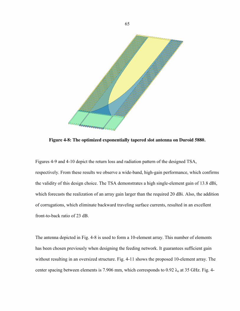
65
Figure 4-8: The optimized exponentially tapered slot antenna on Duroid 5880.
Figures 4-9 and 4-10 depict the return loss and radiation pattern of the designed TSA,
respectively. From these results we observe a wide-band, high-gain performance, which confirms
the validity of this design choice. The TSA demonstrates a high single-element gain of 13.8 dBi,
which forecasts the realization of an array gain larger than the required 20 dBi. Also, the addition
of corrugations, which eliminate backward traveling surface currents, resulted in an excellent
front-to-back ratio of 23 dB.
The antenna depicted in Fig. 4-8 is used to form a 10-element array. This number of elements
has been chosen previously when designing the feeding network. It guarantees sufficient gain
without resulting in an oversized structure. Fig. 4-11 shows the proposed 10-element array. The
center spacing between elements is 7.906 mm, which corresponds to 0.92 λo at 35 GHz. Fig. 4-
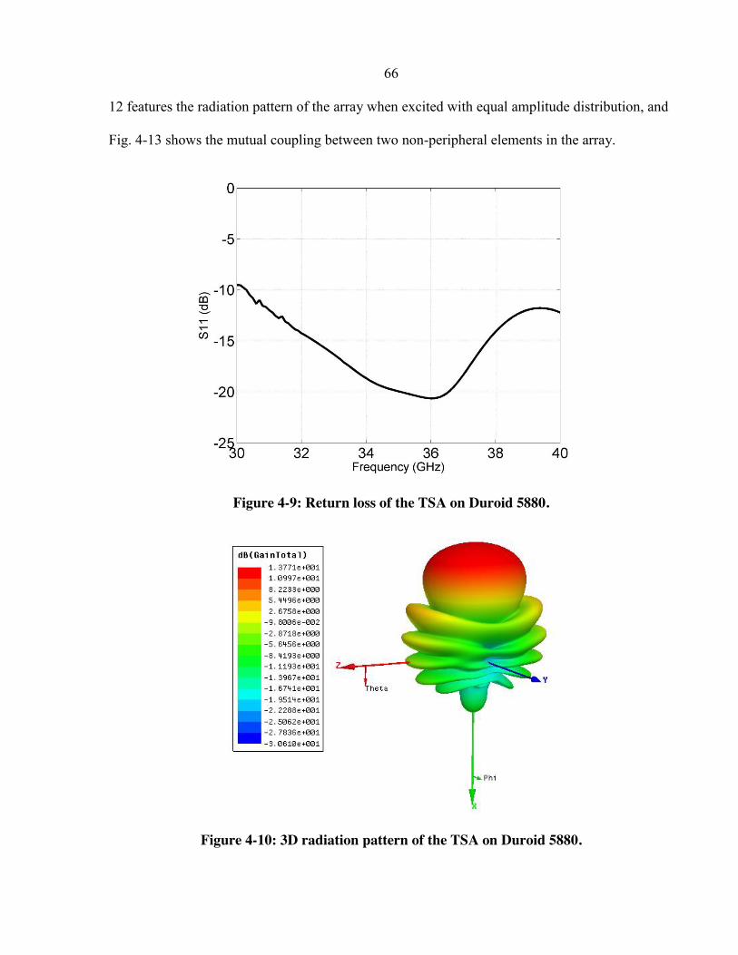
66
12 features the radiation pattern of the array when excited with equal amplitude distribution, and
Fig. 4-13 shows the mutual coupling between two non-peripheral elements in the array.
Figure 4-9: Return loss of the TSA on Duroid 5880.
Figure 4-10: 3D radiation pattern of the TSA on Duroid 5880.
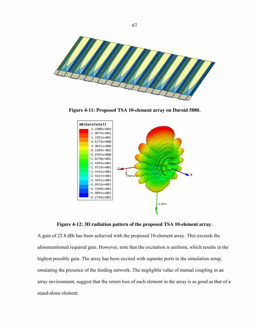
67
Figure 4-11: Proposed TSA 10-element array on Duroid 5880.
Figure 4-12: 3D radiation pattern of the proposed TSA 10-element array.
A gain of 22.8 dBi has been achieved with the proposed 10-element array. This exceeds the
aforementioned required gain. However, note that the excitation is uniform, which results in the
highest possible gain. The array has been excited with separate ports in the simulation setup,
emulating the presence of the feeding network. The negligible value of mutual coupling in an
array environment, suggest that the return loss of each element in the array is as good as that of a
stand-alone element.

68
Figure 4-13: Mutual coupling between two non-peripheral elements in the proposed TSA 10-element array.
4.3 Integration of the Feeding Network and the Antenna Array
With a functioning feeding network and antenna array, the remaining task is to properly integrate
them to form the full passive front-end. The techniques used to establish an efficient transition
from the feeding network to the antenna array are discussed in this section.
4.3.1 Transverse Slot Coupling
In a slotted waveguide array, the slot couples power from the substrate into free air. Using the
same principle, the slot can couple power into other media, such as another substrate. This fact is
exploited in a proposed scheme to transit from an SIW on DuPont 9K7 substrate to another SIW
on Duroid 5880 substrate. In this scheme, a resonant transverse slot is made on the Duroid SIW
top conductor, and power is coupled through this slot to the DuPont SIW aperture. Fig. 4-14
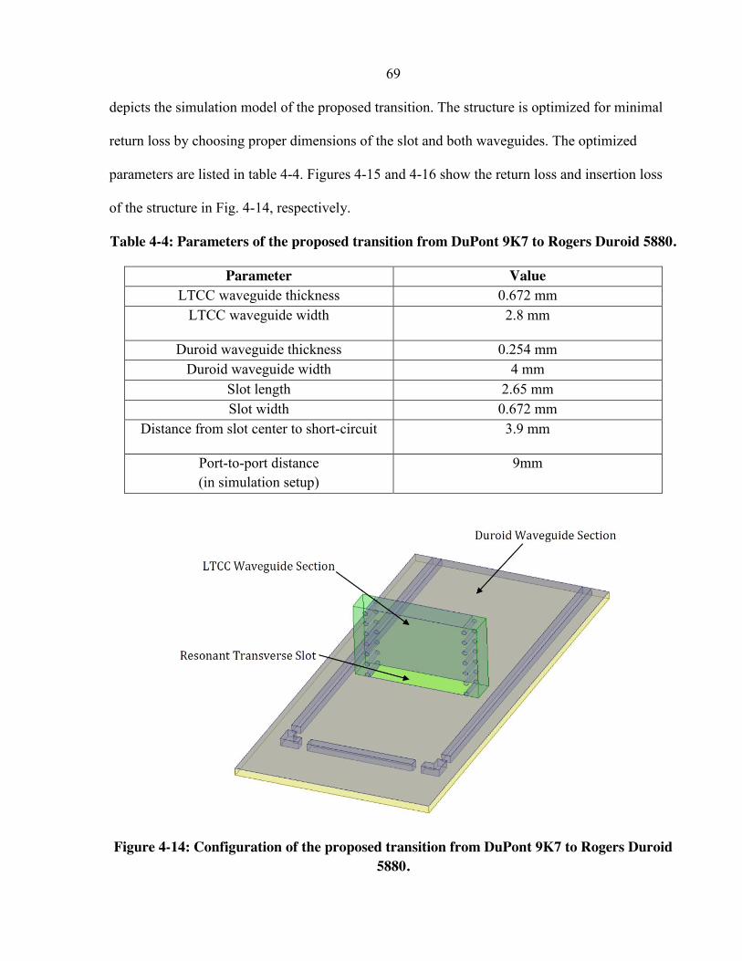
69
depicts the simulation model of the proposed transition. The structure is optimized for minimal
return loss by choosing proper dimensions of the slot and both waveguides. The optimized
parameters are listed in table 4-4. Figures 4-15 and 4-16 show the return loss and insertion loss
of the structure in Fig. 4-14, respectively.
Table 4-4: Parameters of the proposed transition from DuPont 9K7 to Rogers Duroid 5880.
Parameter Value LTCC waveguide thickness 0.672 mm
LTCC waveguide width 2.8 mm
Duroid waveguide thickness 0.254 mm Duroid waveguide width 4 mm
Slot length 2.65 mm Slot width 0.672 mm
Distance from slot center to short-circuit 3.9 mm
Port-to-port distance (in simulation setup)
9mm
Figure 4-14: Configuration of the proposed transition from DuPont 9K7 to Rogers Duroid 5880.
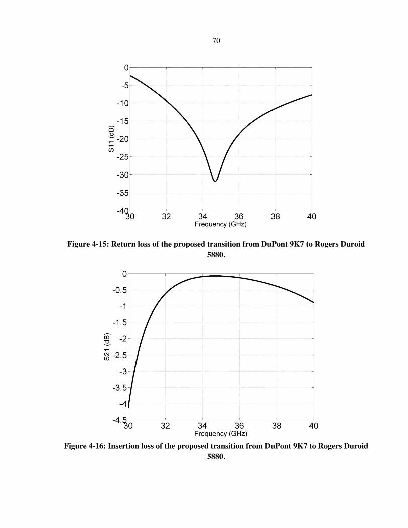
70
Figure 4-15: Return loss of the proposed transition from DuPont 9K7 to Rogers Duroid 5880.
Figure 4-16: Insertion loss of the proposed transition from DuPont 9K7 to Rogers Duroid
5880.

71
Although the transition is resonant, it has very low loss within the bandwidth of interest. Inside this bandwidth, the return loss is better than 14.3 dB.
4.3.2 Waveguide Impedance Transformer
In the previous section, certain dimensions were chosen for the DuPont SIW to properly
incorporate it in an efficient transition to Duroid. These dimensions (both height and width) are
not the same as that of the line used in the feeding network. Changing the width or height of a
waveguide induces reflections arising from junction reactance and impedance change. Thus, the
introduced discontinuities have to undergo careful design.
A theory has been established to transform the impedance of a line without suffering from
reflection loss [43]. It uses a matching section between lines of different impedances. The section
has a nominal length of quarter-wavelength, which means that a wave traveling through the
section and reflected at the end of it traverses half-wavelength to return to its starting position,
thereby causing the destructive interference and diminish of the reflection. Since this effect
occurs at a single frequency, this solution is narrowband. However, the theory expands to
accommodate multiple matching sections, producing the effect at several frequencies, which
results in a wideband solution. Evidently, the number of sections is directly proportional to the
transition bandwidth. Fig. 22 illustrates the multi-section impedance transformer scheme. The
return loss response can be synthesized to have a specific profile such as flat or equal ripple.
Figure 4-17: Schematic circuit of a multi-section λ/4 impedance transformer [44].

72
To design the transition, the return loss profile, the number of matching sections, and the
impedance value of each section have to be chosen. Theoretically, the length of each section
should be a quarter-wavelength, however, the discontinuity at the junctions amidst sections
introduces a reactance, which induces a phase shift. This requires the length correction of each
section to reach the desired matching.
Finding the impedance of each section depends on its response type. For its simplicity, the
binomial impedance transformer [45] has been chosen, and its equations are listed below:
𝐴 ≈ 2 ( ) ln𝑍𝑍
(3)
𝛤 =𝐴 𝑁!
(𝑁 − 𝑛)! 𝑛! (4)
𝑍 = 𝑍 exp (2 𝛤 ) (5)
Where N: the total number of sections. n: the section number. ZL: output section. Zo: input section. 𝛤n: marginal reflection coefficient
Basically, knowing the number of sections, the input impedance, and output impedance, one can
calculate A from (3). Then, the marginal reflection coefficients are found for each value of n
(n=0-N). Finally, the values of impedances are found in an iterative fashion (i.e. Zo finds Z1, and
Z1 finds Z2). This method is implemented to design the proposed transition.
Fig. 4-18 features the proposed equivalent waveguide impedance transformation model, and
table 4-5 lists the parameters of the transition. After optimizing the transition using equivalent
waveguides, they were transformed to SIWs. Fig. 4-19 shows the SIW implementation of the
multi-section impedance transformer, and figures 4-20 and 4-21 depict the return loss and
insertion loss of the structure in Fig. 4-19, respectively. Since the transformer employes a high
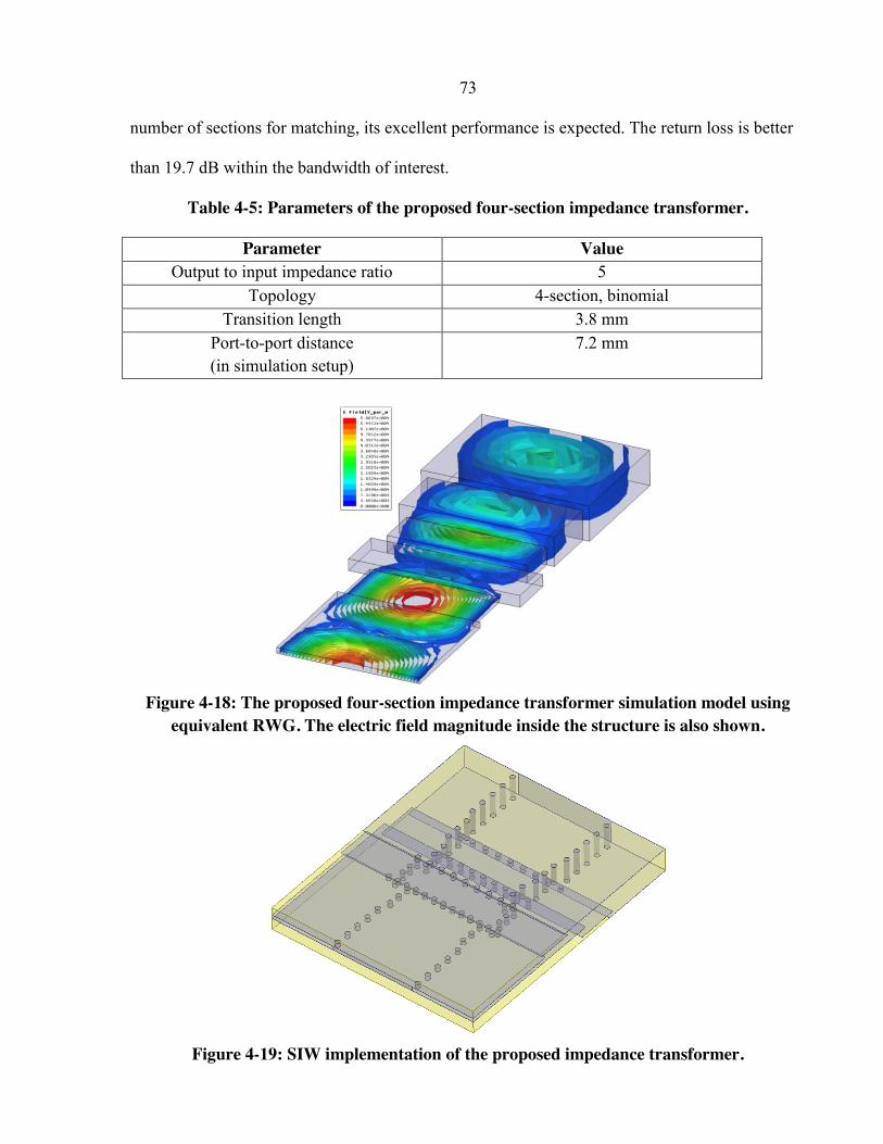
73
number of sections for matching, its excellent performance is expected. The return loss is better
than 19.7 dB within the bandwidth of interest.
Table 4-5: Parameters of the proposed four-section impedance transformer.
Parameter Value Output to input impedance ratio 5
Topology 4-section, binomial Transition length 3.8 mm
Port-to-port distance (in simulation setup)
7.2 mm
Figure 4-18: The proposed four-section impedance transformer simulation model using
equivalent RWG. The electric field magnitude inside the structure is also shown.
Figure 4-19: SIW implementation of the proposed impedance transformer.
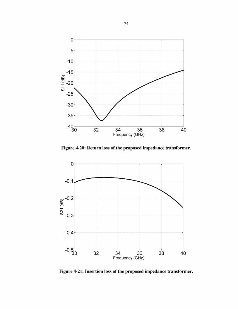
74
Figure 4-20: Return loss of the proposed impedance transformer.
Figure 4-21: Insertion loss of the proposed impedance transformer.

75
4.4 Full Passive Front-End
After confirming the functionality of all the separate components, the next step is to
validate their successful integration. Fig. 4-22 shows the full integrated passive front-end.
The following figures feature various aspects of its performance. The simulated results are
promising with a realized gain of 20 dBi and a maximum side-lobe level of -21 dB at 35
GHz. The return loss is below -10 dB and the gain changes slightly throughout the
bandwidth of interest. Also, the radiation efficiency is above 91%. It can be seen after
observing figures 4-26, 4-27, and 4-28, that the beam shape changes slightly throughout
the bandwidth. Minor side-lobe level increase and gain decrease occur on the bandwidth
boundaries (33 and 37 GHz). The E-plane radiation pattern is expectedly broad, since it
does not lie on the direction of the array extension.

76
Figure 4-22: Full integrated passive front-end.
Figure 4-23: 3D realized gain of the passive front-end.
MS-to-SIW Transition
LTCC Feeding Network
Impedance Transformer
Coupling Slot Antenna Element
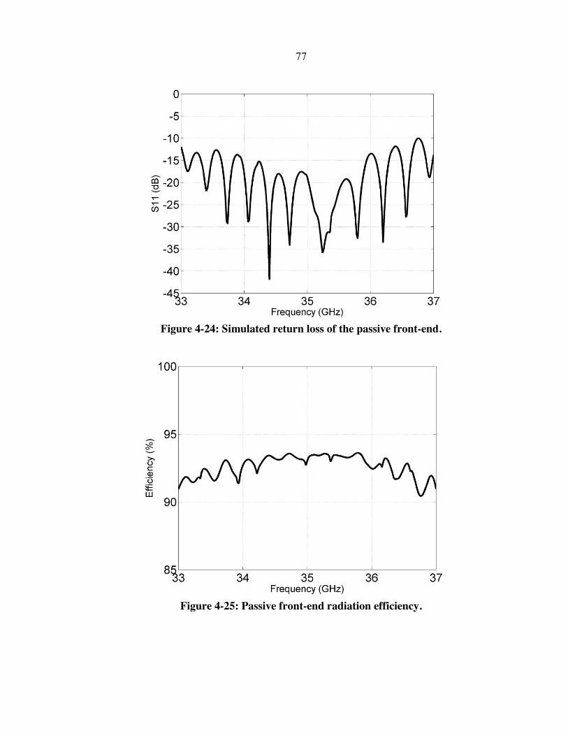
77
Figure 4-24: Simulated return loss of the passive front-end.
Figure 4-25: Passive front-end radiation efficiency.
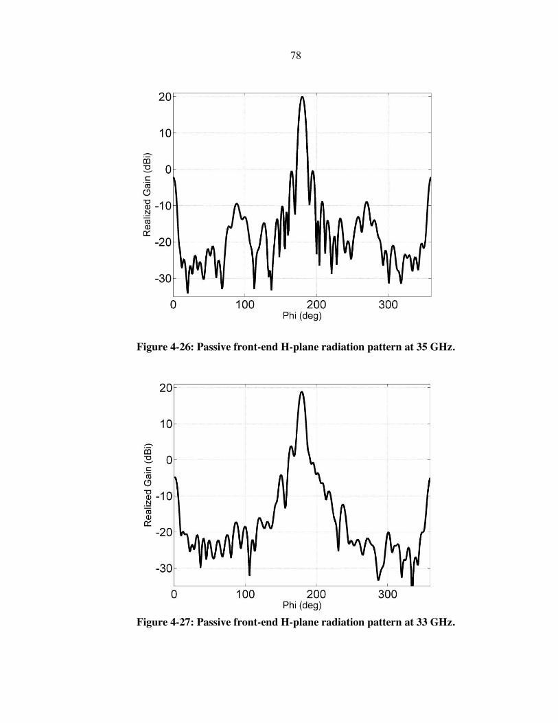
78
Figure 4-26: Passive front-end H-plane radiation pattern at 35 GHz.
Figure 4-27: Passive front-end H-plane radiation pattern at 33 GHz.
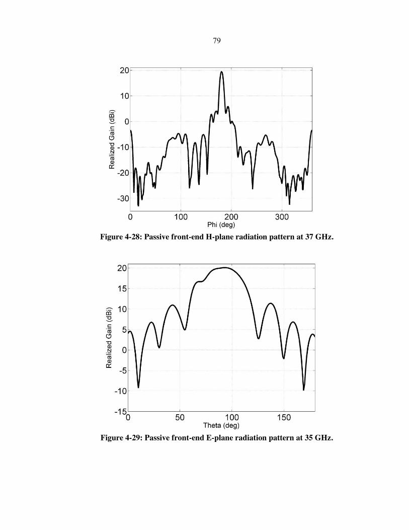
79
Figure 4-28: Passive front-end H-plane radiation pattern at 37 GHz.
Figure 4-29: Passive front-end E-plane radiation pattern at 35 GHz.

80
This module has been fabricated and assembled as shown in figures 4-30 and 4-31, and its return
loss has been measured. Although LTCC technology permits soldering, the specific sheets that
were fabricated must not be soldered. This is because their conductor sheets could be removed in
the process. To solve this issue, two metallic bases are glued to the LTCC substrate and then
soldered to the Duroid substrate, this way the structures merge properly without applying the
solder directly on the LTCC sheets.
The proper lateral shrinkage factor of the LTCC sheets is 9.1%, however, for reasons mentioned
earlier, the actual measured shrinkage is 6.4%. With this change, the perfect coincidence of the
LTCC waveguide aperture and the Duroid coupling slot is no longer valid. To re-align them, a
second Duroid prototype is fabricated with modified dimensions. Re-fabricating the Rogers
substrate is a much simpler and less expensive choice than re-fabricating the LTCC module. The
abovementioned changes in structure sizes were applied to the simulation model. This allows a
more accurate result comparison. Fig. 4-32 depicts the simulated versus measured results of the
modified front-end, and a general matching is observed.
The base developed (shown in Figures 4-30 and 4-31) is not compatible with the test setup in the
anechoic chamber, therefore, the radiation pattern of the full structure could not be measured.
However, a new base is being developed, which is compatible with the gain measurement setup.
Nevertheless, the correlation of the measured and simulated return loss, gives us confidence that
the measured radiation pattern would be quite similar to its simulated value.
Table 4-6 compares the presented passive front-end with state-of-the-art SIW implementations of
integrated arrays. It can be seen that the presented structure is the smallest with one exception
which is Ref. [26]. However, in that work, the bandwidth is much narrower, the radiation
efficiency is lower, and the gain is small for a design at 62 GHz.
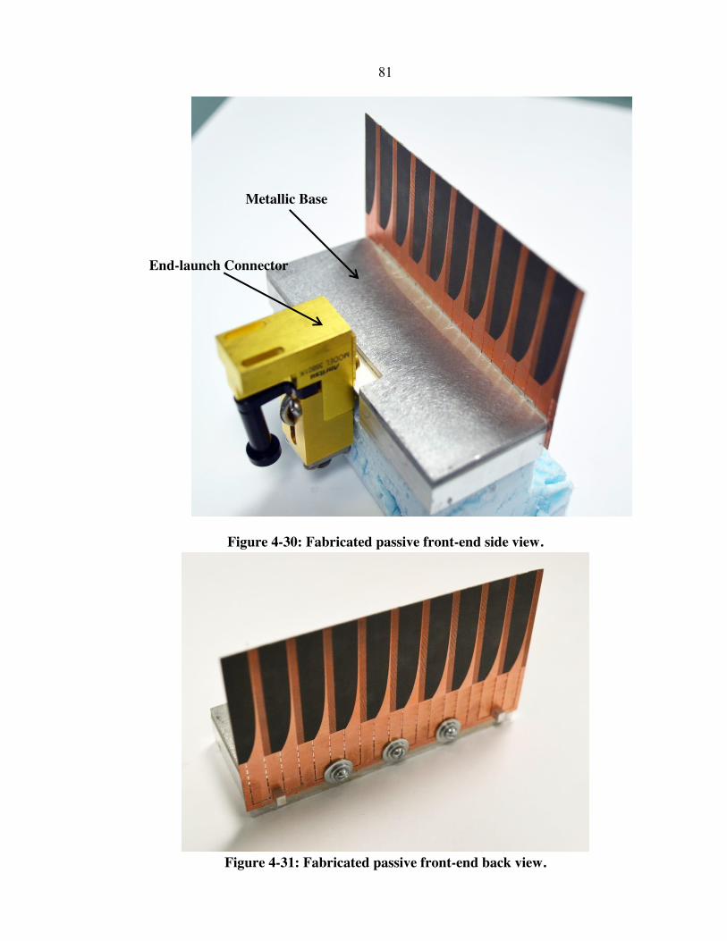
81
Figure 4-30: Fabricated passive front-end side view.
Figure 4-31: Fabricated passive front-end back view.
End-launch Connector
Metallic Base

82
Figure 4-32: Simulated versus measured return loss of the full structure.
Table 4-6: A comparison between the presented passive front-end and SIW
implementations of integrated antenna arrays.
Reference
Antenna Type
Design Frequency
Number of
Antenna Elements
Gain (dBi)
Radiation Efficiency
-10 dB
Bandwidth
Volume
[25] (Fig. 2-10)
Microstrip Patch 12.5 GHz 32 22.5 71% (Measured)
6% > 976 o
[26]
(Fig. 2-11)
Parallel Microstrip
Chain
62 GHz
32
22
74%
(Simulated)
7.6%
135 o
[27]
(Fig. 2-12)
Open-Ended Substrate Integrated Cavities
60 GHz
64
22.1
54.7%
(Simulated)
17.1%
553 o
[28]
(Fig. 2-13)
Dielectric Rod
11 GHz
8
16.5
N/A
31%
502 o
[29]
(Fig. 2-14)
Fermi Tapered Slot Antenna
35 GHz
16
23.4
79%
(N/A)
23.12%
734 o
This work
Exponentially Tapered Slot
Antenna
35 GHz
10
20
92%
(Simulated)
11.4%
285 o

83
5 Conclusion
5.1 Conclusions
The presented work in this thesis discusses the miniaturization of passive front-ends which are
used in PMMW imaging. To perform the miniaturization, two compatible technologies were
used, namely, SIW and LTCC. Using these technologies, a novel, efficient, and compact passive
front-end was designed and fabricated.
The individual components, which are involved in the design, were also fabricated. Some of the
components were measured, and their results are close to simulations. The return loss of the
complete passive front-end has also been measured, and a correlation is observed with its
simulated counterpart. Although the radiation pattern of the complete structure has not been
acquired, the agreement found in the return loss, as mentioned earlier, gives us confidence that
the actual radiation pattern closely resembles simulations.
5.2 Future Work
To enhance the impact of this thesis and further expand its reach, more work has to be completed
as listed below:
Since dual-polarization is important for this application, the next step should be to extend
the passive front-end to accommodate it. This would be done by connecting two identical
orthogonal front-ends and testing the acquired image using this scheme to validate its
functionality.

84
The final structure was formed using two separate substrates, which deviates from the
original plan of a monolithic module. A solution exists to realize that plan. Liquid
Crystalline Polymer (LCP) is a promising high-frequency substrate which can be used to
make multilayer structures [46]. Also, the dielectric constant of LCP is typically lower
than three, and since vias and conductor sheets are employed in LCP, the same passive
front-end presented in this thesis could be formed in one substrate while maintaining the
targeted performance.
In the proposed design, the number of layers increased linearly with the number of power
division stages. This arrangement is not necessary, but was rather done to simplify the
design and render it systematic. By filling up empty vicinities within each layer and
alternating between them to form the feeding network, the number of layers could be
reduced by as much as half. However, the approach in realizing such a complicated
structure is artistic, which requires creating a library of architectures for feeding networks
of different sizes.

85
References
[1] L. Yujiri, M. Shoucri, and P. Moffa, "Passive millimeter wave imaging," Microwave Magazine, IEEE, vol. 4, pp. 39-50, 2003.
[2] F. T. Ulaby, A. K. Fung, and R. K. Moore, Microwave remote sensing, fundamentals and radiometry. Norwood, Mass: ARTECH House, 1981.
[3] J. A. Lovberg, C. Martin, and V. Kolinko, "Video-Rate Passive Millimeter-Wave Imaging Using Phased Arrays," in Microwave Symposium, 2007. IEEE/MTT-S International, 2007, pp. 1689-1692.
[4] L. Golonka, "Technology and applications of low temperature cofired ceramic (LTCC) based sensors and microsystems," TECHNICAL SCIENCES, vol. 54, 2006.
[5] D. Deslandes and K. Wu, "Integrated microstrip and rectangular waveguide in planar form," Microwave and Wireless Components Letters, IEEE, vol. 11, pp. 68-70, 2001.
[6] N. Skou and D. Le Vine, Microwave radiometer systems : design and analysis. Boston, Mass. [u.a.]: Artech House, 2006.
[7] H. Abuzaid, A. Doghri, A. Shamim, and K. Wu, "SIW Based Mutlilayer Transition and Power Divider in LTCC Technology," presented at the International Microwave Symposium (IMS), Seattle, WA, USA, 2013 (accepted).
[8] J. Burns, L. McIlrath, C. Keast, C. Lewis, A. Loomis, K. Warner, et al., "Three-dimensional integrated circuits for low-power, high-bandwidth systems on a chip," in Solid-State Circuits Conference, 2001. Digest of Technical Papers. ISSCC. 2001 IEEE International, 2001, pp. 268-269, 453.
[9] B. Lopez-Garcia, D. V. B. Murthy, J. Soto-Manriquez, and A. Corona-Chavez, "Passive Millimeter-wave imaging using a Substrate Integrated Waveguide antenna," in Infrared, Millimeter and Terahertz Waves, 2008. IRMMW-THz 2008. 33rd International Conference on, 2008, pp. 1-2.
[10] N. Skou, Microwave radiometer systems--design and analysis. Norwood, MA: Artech House, 1989.
[11] P. F. Goldsmith, C. T. Hsieh, G. R. Huguenin, J. Kapitzky, and E. L. Moore, "Focal plane imaging systems for millimeter wavelengths," Microwave Theory and Techniques, IEEE Transactions on, vol. 41, pp. 1664-1675, 1993.
[12] D. Vye. (2011). Available: http://www.microwavejournal.com/articles/11995-divine-innovation-10-technologies-changing-the-future-of-passive-and-control-components
[13] L. Yan, W. Hong, G. Hua, J. Chen, K. Wu, and T. J. Cui, "Simulation and experiment on SIW slot array antennas," Microwave and Wireless Components Letters, IEEE, vol. 14, pp. 446-448, 2004.
[14] M. Shahabadi, "Wide-band Amplifiers Based on Substrate Integrated Waveguides," in International Microwave Symposium, Montreal, Canada, 2012.
[15] W. Hong and K. Wu, "Design Mechanism and Application Examples of SIW Structure Family," in International Microwave Symposium, Montreal, Canada, 2012.
[16] S. Germain, D. Deslandes, and K. Wu, "Development of substrate integrated waveguide power dividers," in Electrical and Computer Engineering, 2003. IEEE CCECE 2003. Canadian Conference on, 2003, pp. 1921-1924 vol.3.

86
[17] W. D'Orazio, K. Wu, and J. Helszajn, "A substrate integrated waveguide degree-2 circulator," Microwave and Wireless Components Letters, IEEE, vol. 14, pp. 207-209, 2004.
[18] Z. C. Hao, W. Hong, X. P. Chen, J. X. Chen, K. Wu, and T. J. Cui, "Multilayered substrate integrated waveguide (MSIW) elliptic filter," Microwave and Wireless Components Letters, IEEE, vol. 15, pp. 95-97, 2005.
[19] X. Xu, R. G. Bosisio, and K. Wu, "A new six-port junction based on substrate integrated waveguide technology," Microwave Theory and Techniques, IEEE Transactions on, vol. 53, pp. 2267-2273, 2005.
[20] J.-X. Chen, W. Hong, Z.-C. Hao, H. Li, and K. Wu, "Development of a low cost microwave mixer using a broad-band substrate integrated waveguide (SIW) coupler," Microwave and Wireless Components Letters, IEEE, vol. 16, pp. 84-86, 2006.
[21] Y. J. Cheng, W. Hong, K. Wu, Z. Q. Kuai, C. Yu, J. X. Chen, et al., "Substrate Integrated Waveguide (SIW) Rotman Lens and Its Ka-Band Multibeam Array Antenna Applications," Antennas and Propagation, IEEE Transactions on, vol. 56, pp. 2504-2513, 2008.
[22] Y. Ding and K. Wu, "Varactor-tuned substrate integrated waveguide phase shifter," in Microwave Symposium Digest (MTT), 2011 IEEE MTT-S International, 2011, pp. 1-4.
[23] F. Zhu, W. Hong, J. X. Chen, and K. Wu, "Design and Implementation of a Broadband Substrate Integrated Waveguide Magic-T," Microwave and Wireless Components Letters, IEEE, vol. 22, pp. 630-632, 2012.
[24] M. R. Gongora-Rubio, P. Espinoza-Vallejos, L. Sola-Laguna, and J. J. Santiago-Avilés, "Overview of low temperature co-fired ceramics tape technology for meso-system technology (MsST)," Sensors and Actuators A: Physical, vol. 89, pp. 222-241, 4/15/ 2001.
[25] A. Borji, D. Busuioc, and S. Safavi-Naeini, "Efficient, Low-Cost Integrated Waveguide-Fed Planar Antenna Array for Ku-Band Applications," Antennas and Wireless Propagation Letters, IEEE, vol. 8, pp. 336-339, 2009.
[26] A. Lamminen and J. Saily, "High gain 60 GHz LTCC chain antenna array with substrate integrated waveguide feed network," in Antennas and Propagation (EUCAP), 2012 6th European Conference on, 2012, pp. 2569-2573.
[27] J. Xu, Z. N. Chen, X. Qing, and W. Hong, "Bandwidth Enhancement for a 60 GHz Substrate Integrated Waveguide Fed Cavity Array Antenna on LTCC," Antennas and Propagation, IEEE Transactions on, vol. 59, pp. 826-832, 2011.
[28] R. Kazemi, A. E. Fathy, and R. A. Sadeghzadeh, "Dielectric Rod Antenna Array With Substrate Integrated Waveguide Planar Feed Network for Wideband Applications," Antennas and Propagation, IEEE Transactions on, vol. 60, pp. 1312-1319, 2012.
[29] B. Y. El Khatib, T. Djerafi, and K. Wu, "Three-Dimensional Architecture of Substrate Integrated Waveguide Feeder for Fermi Tapered Slot Antenna Array Applications," Antennas and Propagation, IEEE Transactions on, vol. 60, pp. 4610-4618, 2012.
[30] N. Marcuvitz, Waveguide handbook. London, UK: P. Peregrinus on behalf of the Institution of Electrical Engineers, 1986.
[31] Y. Cassivi, L. Perregrini, P. Arcioni, M. Bressan, K. Wu, and G. Conciauro, "Dispersion characteristics of substrate integrated rectangular waveguide," Microwave and Wireless Components Letters, IEEE, vol. 12, pp. 333-335, 2002.
[32] G. Conciauro, M. Guglielmi, and R. Sorrentino, Advanced modal analysis : CAD techniques for waveguide components and filters. Chichester; New York: Wiley, 2000.

87
[33] D. Deslandes and K. Wu, "Accurate modeling, wave mechanisms, and design considerations of a substrate integrated waveguide," Microwave Theory and Techniques, IEEE Transactions on, vol. 54, pp. 2516-2526, 2006.
[34] C. A. Balanis, Antenna theory analysis and design, 3rd ed. Hoboken, N.J.: Wiley-Interscience, 2005.
[35] R. C. Johnson and H. Jasik, Antenna engineering handbook, 2nd ed., 1984. [36] G. L. Chen, T. L. Owens, and J. H. Whealton, "Theoretical study of the folded
waveguide," Plasma Science, IEEE Transactions on, vol. 16, pp. 305-311, 1988. [37] D. Deslandes, "Design equations for tapered microstrip-to-Substrate Integrated
Waveguide transitions," in Microwave Symposium Digest (MTT), 2010 IEEE MTT-S International, 2010, pp. 704-707.
[38] T. Djerafi and K. Wu, "Corrugated Substrate Integrated Waveguide (SIW) Antipodal Linearly Tapered Slot Antenna Array Fed by Quasi-Triangular Power Divider," Progress In Electromagnetics Research C, vol. 26, pp. 139-151, 2012.
[39] H. Wang, D.-G. Fang, B. Zhang, and W.-Q. Che, "Dielectric Loaded Substrate Integrated Waveguide (SIW) H-Plane Horn Antennas," Antennas and Propagation, IEEE Transactions on, vol. 58, pp. 640-647, 2010.
[40] D. Schaubert, E. Kollberg, T. Korzeniowski, T. Thungren, J. Johansson, and K. Yngvesson, "Endfire tapered slot antennas on dielectric substrates," Antennas and Propagation, IEEE Transactions on, vol. 33, pp. 1392-1400, 1985.
[41] S. Sugawara, Y. Maita, K. Adachi, K. Mori, and K. Mizuno, "Characteristics of a MM-wave tapered slot antenna with corrugated edges," in Microwave Symposium Digest, 1998 IEEE MTT-S International, 1998, pp. 533-536 vol.2.
[42] Z. C. Hao, W. Hong, J. X. Chen, X. P. Chen, and K. Wu, "A novel feeding technique for antipodal linearly tapered slot antenna array," in Microwave Symposium Digest, 2005 IEEE MTT-S International, 2005, p. 3 pp.
[43] H. J. Riblet, "General Synthesis of Quarter-Wave Impedance Transformers," Microwave Theory and Techniques, IRE Transactions on, vol. 5, pp. 36-43, 1957.
[44] Y. Yun, "A miniaturized multisection transformer on Si RFIC for low impedance transformation in UWB," Microwave Journal, vol. 53, pp. 76-82, 2010.
[45] D. Misra, W. John, and Sons. (2001). Radio-frequency and microwave communication circuits analysis and design, pp. 244.
[46] G. Zou, H. Gronqvist, J. P. Starski, and J. Liu, "Characterization of liquid crystal polymer for high frequency system-in-a-package applications," Advanced Packaging, IEEE Transactions on, vol. 25, pp. 503-508, 2002.