Embed Size (px)
Citation preview

An Efficient VLSI Architecture of Fractional MotionEstimation in H.264 for HDTV
G. A. Ruiz & J. A. Michell
Received: 17 September 2009 /Revised: 9 March 2010 /Accepted: 11 March 2010# Springer Science+Business Media, LLC 2010
Abstract Fractional Motion Estimation (FME) in high-definition H.264 presents a significant design challenge interms of memory bandwidth, latency and area cost as thereare various modes and complex mode decision flow, whichrequire over 45% of the computation complexity in theH.264 encoding process. In this paper, a new high-performance VLSI architecture for Fractional MotionEstimation (FME) in H.264/AVC based on the full-searchalgorithm is presented. This architecture is made up of threedifferent pipeline processors to establish a trade-off be-tween processing time and hardware utilization. Thecomputing scheme based on a 4-pixel interpolation unitwith a 10-pixel input bandwidth is capable of processing amacroblock (MB) in 870 clock cycles. The final VLSIimplementation only requires 11.4 k gates and 4.4kBytes ofRAM in a standard 180 nm CMOS technology operating at290 MHz. Our design generates the residual image and thebest MVs and mode in a high throughput and low area costarchitecture while achieving enough processing capacity for1080HD (1920×1088@30fps) real-time video streams.
Keywords H.264 . High-definition television (HDTV) .
Fractional motion estimation . Video coding
1 Introduction
The video coding standard H.264/AVC, developed by theJoint Video Team (JVT), achieves higher coding efficiency
than previous coding standards especially in high-definitionand high-rate video sequences. The superior codingperformance of H.264/AVC originates from new techniquessuch as quarter-pixel fractional motion estimation, variableblock sizes, multiple reference frame motion estimation,complex intra prediction modes, context-based entropycoding, and so on [1, 2]. However, these advanced videocoding techniques require huge computational complexityand memory bandwidth for the encoding process. Thus,hardware acceleration encoder design is still essential toenable implementation of fast architectures for real-timevideo applications.
Motion estimation (ME) is the most important part ofH.264/AVC in exploiting the temporal redundancy betweensuccessive frames and it is also the most time consumingpart in the coding framework. It requires large amounts ofcomputation and accounts for 60%–90% of encoding time.In H.264, a video frame is first split using macroblocks(MB) of size 16×16 [3]. Each MB may then be segmentedinto subblocks of different sizes, as illustrated in Fig. 1. MEis carried out in 7 different modes, one 16×16 MB (Mode1), two 16×8 subblocks (Mode 2), two 8×16 subblocks(Mode 3) and four 8×8 subblocks (Mode 4). In turn, each8×8 subblock is also split up into two 8×4 subblocks(Mode 5), two 4×8 subblocks (Mode 6) and four 4×4subblocks (Mode 7). The total number of possible partitionsis 41. ME refines the best candidate for each subblockshierarchy in two phases: Integer Motion Estimation (IME)and Fractional Motion Estimation (FME). IME finds thebest integer motion vector (MV) for all 41 variable-sizeblocks. FME refines those MVs in quarter-pixel precisionusing a 6-tap filter and a MV-bit-rate estimation. In H.264/AVC, the latter process takes about 45% of ME time and,for high resolution application, VLSI implementation isessential.
G. A. Ruiz (*) : J. A. MichellDpto. de Electrónica y Computadores, Facultad de Ciencias,Universidad de Cantabria,Avda. de Los Castros s/n,39005 Santander, Spaine-mail: [email protected]
J Sign Process SystDOI 10.1007/s11265-010-0475-8

There are many proposed IME algorithms based on one-dimension [5] or two-dimension [6] processing elements,different search strategies such as the three-step search [7],hexagon search [8] and diamond search [9], or implemen-tations aiming to reduce the power [10] or to minimize theoff-chip memory bandwidth [11]. However, only a fewFME implementations have been discussed in spite of FMEhaving a strong impact on the peak-signal-to-noise ratio(PSNR) and the amount of computation required for FMEis even more than needed for IME. Several algorithms havebeen proposed to speed up the FME process, although theydecrease the video quality to some extent, such as those basedon early termination techniques [12] (average ΔPSNR=−0.02 dB, ΔBitrate=2.91%), search control by using neigh-bouring motion vectors [13] (ΔPSNR=−0.03 dB), sizereduction of tap filters [14] (ΔPSNR=−0.003 dB) orreduction of search area [15] (ΔPSNR=−0.17 dB, ΔBitrate=4.08%). Different FME implementations which make atrade-off among input bandwidth of reference pixels,hardware overhead and number of clock cycles for process-ing all MBs have been described. In [16], VLSI architecturefor FME with a regular schedule and high utilization ispresented. It uses a 4-pixel interpolation unit to process 10integer pixels in parallel at 100 MHz taking 1648 clockcycles to compute a whole macroblock (MB). An improvedarchitecture with a 16-pixel interpolation unit to reduce thisnumber of cycles to 790 is described in [17]. It achieves highprocessing capacity for encoding real-time HDTV videostreams. However, this high throughput has the penalty oflarge area (2.4×) and memory bandwidth up to 22 pixels. Ahigh throughput hardware architecture based on three parallelprocessing engines reduces the number of clock cycles toonly 616, but with a high cost in area [19]. Other FMEdesigns search for hardware reduction or high efficiency bymaking some constraints in the FME algorithm. Thus, thescheme proposed in [20] achieves a reduction of more than50% in computation by exploring neighbourhood positionand early termination with acceptable loss of quality. Thearchitecture described in [21] reduces the search area and
number of MVs needed in order to achieve low-latency andhardware efficiency. Finally, designs suitable for a FPGAimplementation are presented in [22, 23]
In this paper, a VLSI architecture based on the full-searchalgorithm for implementation of FME is described. Itsarchitecture is made up of three different pipeline processors:a half-pixel processor, a quarter-pixel processor and a modedecision processor. As a result, our design generates theresidual image and the best MVs in a high throughput, lowarea cost architecture. The design is implemented with only11.4 k gates and 4.4kBytes of RAM in a standard 180 nmCMOS technology and it operates at 290 MHz. The latencyof 870 clock cycles is sufficiently low to process 1080HDreal-time videos. The remainder of this paper is organized asfollows. In Section 3, a brief description of the FME schemeis discussed. Section 4 presents some details of the proposedarchitecture based on three processors, and Sections 5, 6 and7 describe some details about the design of those processors.The implementation results and comparisons are listed inSection 7. Finally, the conclusions are stated in Section 8.
2 Description of the FME Algorithm
In H.264, the inter-prediction module is one of the mostsignificant parts that affect overall computing performance.In real-time HDTV applications (1920×1088 @ 30fps) thework of processing all 41 subblocks belonging to a 16×16 MB should take less than 4.1 µsec, equivalent to 1025clock cycles at a clock frequency of 250 MHz, which isavailable for most of current technologies. IME and FMEmust be computed in these 1025 cycles which will affectthe efficiency of the hardware implementation. IME isperformed prior to FME. Integer pixel search tries to findthe best matching integer position and the best integer pixelmotion vectors (MV) are determined by using a perfor-mance cost metric. Then, the FME performs a half-pixelrefinement about the integer search positions and then aquarter-pixel one is performed around the best half-pixel
00
10 1
0 1
2 3
01
0 10 12 3
Mode 1 (16×16) Mode 3 (8×16)Mode 2 (16×8) Mode 4 (8×8)
Mode 6(4×8)
Mode 5(8×4)
Mode 7(4×4)
Figure 1 Sub-macroblockpartitions.
J Sign Process Syst

positions. As a result, a pipeline architecture is a must toimplement IME and FME [24, 25].
In an efficient FME implementation, the trade-off amongprocessing time, memory access data bus and hardwareutilization should be balanced. Here the memory access andsub-pixel interpolation must comply with some timeconstraints, taking into account that FME requires moreinput data to be processed than is used in sub-pixel motionestimation. Besides, FME shares on-chip memory previ-ously stored in the IME stage as FME fetches reference datato that memory when IME has just finished. In our design,a 4-pixel interpolation unit is adopted because it provides atrade-off between the processing time and hardwareutilization, and it is also highly compatible with manyproposed IME architectures. This unit is capable ofprocessing every subblock in a MB, since each subblockcan be decomposed in terms of single 4×4 basic blocks.However, the 6-tap filter used in interpolation processrequests extra input pixels so that each 4×4 subblock isextended with a border of 3 pixels around it, resulting in a(3+4+3)×(3+4+3)=10×10 window; thus, the input data isset to 10 pixels’ width. To reduce accesses to memory andreuse interpolated data, vertically adjacent 4×4 blocks areprocessed using a similar scheme to that proposed in [16],which helps to avoid redundant memory accesses (about25–35% of total bandwidth). In this scheme, vertical scanorder is adopted to facilitate the interpolation operationsbetween two adjacent vertical columns for subblocks of 8×and 16×. For the sake of clarity, Fig. 2 shows the verticalarrangement to carry out the interpolation process of a 16×16 MB. With 10 pixels of input data, the processing of acolumn takes 22 clock cycles, and the whole block 22×4=88 clock cycles. Table 1 lists the clock cycles needed toprocess all 41 different modes, the total number being 832.A problem related to vertical interpolation is the redundantinterpolating operations which appear in the overlappingarea of the adjacent interpolation window. To overcome thisproblem, a new schedule based on a 16-pixel interpolationis proposed in [17], which removes all the redundantcolumns. Although this architecture can save more than50% clock cycles, it uses input data of 22-pixels’ width and
the cost in area is about 2.4 times greater than 4-pixelinterpolation. Moreover, it incurs low computational redun-dancy but is inefficient in handling variable size.
2.1 Langrangian Cost
The ME algorithm determines the best mode whichminimizes the matching error between reference MB andcandidate MB. In the JM version 15.1 of the H.264reference software, which is available on-line at [4], theME chooses the best mode by using a Lagrangian modedecision to compute not only the sum of absolute differ-ences (SAD) but also an estimation of the bits required tocode MVs. For each subblock of a MB, the ME algorithmminimizes the following Langrangian cost (J) defined as
J ¼ SADþ l MV cos t MVcur �MVpredð Þ ð1Þwhere SAD denotes a distortion measure (in our case it isthe SAD) between the original and the coded partitionpredicted from the reference frames, MVcost represents thenumber of bits (according to a table of entropy coding) re-quired to code the difference of current MV (MVcur) andmotion prediction MVpred, and λ is the Langrangianmultiplier imposed using a suitable rate constraint. Tocalculate the MVpred, the MV of the neighbouring blocksmust be available or sufficiently estimated as they not onlydepend on neighbouring MBs, but also on earlier blockswithin a MB [3]. Figure 3 shows an example of definition
10
22 16×16
1010
10
3
3
Figure 2 Vertical interpolationof 16×16 MB.
Table 1 Clock cycling for different subblocks.
Subblock type Number of blocks Cycles/block Total cycles
16×16 1 22×4 88
16×8 2 14×4 112
8×16 2 22×2 88
8×8 4 14×2 112
8×4 8 10×2 160
4×8 8 14×1 112
4×4 16 10×1 160
Total latency 832
MV2MV1
MV0
8×8
MVpred=median(MV0, MV1, MV2)
Fig. 3 Example of MVpred of 8×8 macroblock.
J Sign Process Syst

of MVpred for an 8×8 subblock. In this case, the MVpredis computed from the median of left (MV0), top (MV1) andtop-right (MV2). MV0 belongs to the previous 16×16 MB,and MV1 and MV2 belong to 4×4 subblocks of the sameMB that have just been processed.
The proposed FME algorithm uses the well-known treestructured motion compensation method of H.264 to obtainthe MVpred of each subblock. In this method, the sub-blocks are processed in a particular order to guarantee thatevery MVpred neighbouring a subblock is available beforeprocessing. Otherwise, an incorrect MVpred significantlyworsens coding results because it leads the motionestimation in the wrong direction. The Lagrangian costfunction can only be computed after the MVs of neighbour-ing blocks are determined, which causes an inevitablesequential processing. MBs and subblocks in a MB cannotbe processed in parallel. As a result, while processing asubblock in the half-pixel processor, the MVs of neighboursat quarter resolution are not available because the quarterprocessor has not computed them yet. This problem onlyarises in the subblocks labelled 1 in Fig. 1 belonging to
Mode 2, 3, 4, 5 and 6, and subblocks labelled 1, 2 and 3 inMode 7. In the proposed FME, these subblocks only usehalf pixel resolution in MVpred because MVpreds withquarter resolution are not available. Simulations made withtypical video sequences have proved that the effects of thisrestriction on overall PSNR and bitrate are insignificant(average ΔPSNR=−0.003 dB and ΔBitrate=0.05%).
3 Proposed Architecture
Figure 4 shows the block diagram for the proposed designof FME hardware architecture based on three differentpipeline processors: half-pixel processor, quarter-pixelprocessor and mode decision processor. This architecturemakes a trade-off between the processing time and thehardware utilization to reach the capacity of encoding thehigh-resolution real-time video stream for HDTV at lowcost in area. It uses a completely standard-compatible full-search algorithm based on 4×4 block decomposition and avertical arrangement to reduce the encoding time.
f
RAM118x18 I18x17 H17x18 V17x17 D
LocalRAM
Reference Frame
Current Frame
LocalRAM
Half-pixelinterpolation10 I,H,V,D
Parallel processing Unit
Parallel processing Unit
Quarter-pixelinterpolation
2304 pixels
RAM2
MODEDECISION
Residualimage
Half -pixel
RAM3
Quarter -pixel
Half-pixel processor
Quarter-pixelprocessor
Mode decision processor
Best MVs & Mode
4
512 pixels
Best Half-MV
BestQuarter-
MV
4
2304 pixels
14
22
36
32
4
H
PE1 PE8
MV cos t
PE1 PE8
MV cos t
5
V
4
D
5
C
I
Figure 4 Block diagram ofgeneral FME architecture.
J Sign Process Syst

The input data include the best integer MV with itsLangrangian cost acquired in IME, MVpred of the adjacentMBs and search area data from a local memory which isinput row by row. The half-pixel processor reads thereference input data from a local RAM and performs half-pixel interpolation and a full half-pixel search for eachsubblock size. The interpolated samples are stored inRAM1 and processed in the processing unit. This unit ismade up of 8 parallel processing elements (PE) to obtainthe best half-MV according to minimum Lagrangian cost.The quarter-pixel processor uses the best half-MV and theinterpolated samples stored in RAM1 to generate all thequarter-pixels around the half/integer samples using abilinear filter. These are stored in RAM2. Similarly to theprevious processor, these interpolated quarter-pixels areprocessed in the processing unit in order to extract the bestquarter-MVs. After that, the mode decision processorevaluates, temporarily stores the best matching interpolatedimage in RAM3 and makes a decision about block modesand final MVs. However, the final decision is not takenuntil all 41 subblocks are processed. Finally, this processorgenerates the best MVs and the best mode of the MB, aswell as the residual image to be coded.
Figure 5 depicts the timing diagram for performing FMEto process one MB. It dispatches all 41 subblocks rangingfrom 16×16 to 4×4 reads according to the tree-structuredmotion compensation order specified in the JM referencesoftware. The input reading process consumes 832 clockcycles (see Table 1) to load all input data which bounds thewhole processing time. The half-pixel processor performs ahalf-pixel interpolation, which is stored in a bank of four
double port SRAMs (RAM1), and takes a decision aboutthe best half-MV after computing the Langrangian cost. Ontaking this decision, the quarter-pixel processor starts offfetching data to RAM1. Here, the reading process takesfewer clock cycles than the former processor; for a M×Nsubblock, it takes (M+1)×N/4 clock cycles in comparisonwith the former’s (M+6)×N/4. As a result, this quarter-pixel processor has idle clocks waiting to finish theprocessing of some subblocks in the half-pixel processor.After taking the best quarter-MVs decision and computinga new Langragion cost, the mode decision processor startsoff fetching data to a bank of three double-port SRAMs(RAM2). The reading process takes the same number ofclock cycles as the size of the processing subblock (M×N);there are also some idle clock cycles here. The candidatesamples specified by the best quarter-MVs are stored inRAM3 according to a scheme described in Section 7. After870 clock cycles, the final decision is taken by processingall 41 subblocks. The proposed architecture for generatingthe residual image of a MB takes a total of 936 clockcycles: 832 cycles for reading the input data, 38 cycles oflatency and 66 cycles to generate the residual image.
4 Half-Pixel Processor
The half-pixel processor performs half-pixel interpolationand a half-pixel search for each subblock. It is mainlycomposed of a half-pixel interpolation unit, four double-port SRAMs (RAM1) to store integer and half-pixelsamples, a processing unit (PU) to compute the Lagrangian
16◊16 8◊16 8◊16 16◊8
88 56 56 44
16◊8
44
8◊8
28
16◊16
68 36
8◊16
36
8◊16
34
16◊8
Input data
Half interpolation
Write RAM1Best half-MV
Read RAM1
Quarter interpolation
Best quarter-MVWrite RAM2
64Read RAM2
Write RAM3
32 32
Decision best MV
4◊4
1010 10
10
8
10
5
444
Residual image & best MVs64
555
48
cycle
0 832 870 936
Hal
f-pi
xel
proc
esso
r
Qua
rter
-pix
elpr
oces
sor
Mod
ede
cisi
onpr
oces
sor
8◊8
Figure 5 Timing diagram for performing FME for one MB.
J Sign Process Syst

cost, and a best half MV unit to select the MVs withminimum Lagrangian cost. As a result, the best MVs arepassed to the quarter-pixel processor.
4.1 Half-Pixel Interpolation Unit
In the H.264/AVC, the prediction luma sample values at thehalf pixel are calculated by applying a 6-tap Wiener filter inboth horizontal and vertical directions. The tap coefficientsare (1, −5, 20, 20, −5, 1). For the sake of clarity, Fig. 6illustrates the spatial relationship of the integer {I}, andhalf-pixel vertical {V}, horizontal {H} and diagonal {D}positions in the luminance interpolation. The horizontalhalf-pixel value H0,0 is computed from an intermediatevalue H
00;0 which is calculated in turn from the six nearest
integer pixel values located at horizontal direction accord-ing to the following equation
H00;0 ¼ I0;�2 � 5I0;�1 þ 20I0;0 þ 20I0;1 � 5I0;2 þ I0;3 ð2ÞThe half sample H0,0 is calculated by clipping H
00;0to lie
in the range [0,255] as
H0;0 ¼ H00;0 þ 1 << 4
� �>> 5 ð3Þ
In a similar way, the vertical half-pixel value V0,0 iscalculated from an intermediate value V
00;0 using the six
nearest integer pixel values located in the vertical direction as
V00;0 ¼ I�2;0 � 5I�1;0 þ 20I0;0 þ 20I1;0 � 5I2;0 þ I3;0 ð4Þ
The half sample V0,0 is calculated by clipping V00;0to the
range [0,255] as
V0;0 ¼ V00;0 þ 1 << 4
� �>> 5 ð5Þ
The diagonal half-pixel value D00;0 is obtained from the
six nearest intermediate horizontal values H0i;j, or alterna-
tively, vertical values V0i;j, according to
D00;0 ¼ H
0�2;0 � 5H
0�1;0 þ 20H
00;0 þ 20H
01;0 � 5H
02;0
þ H03;0 ð6Þ
D00;0 ¼ V
00;�2 � 5V
00;�1 þ 20V
00;0 þ 20V
00;1 � 5V
00;2
þ V00;3 ð7Þ
The final value D0,0 is computed as
D0;0 ¼ D00;0 þ 1 << 9
� �>> 10 ð8Þ
Figure 7 shows the proposed interpolator architecturebased on a 2-D FIR approach which aims for highthroughput and minimum latency. The 2-D FIR is decom-posed into 1-D FIR horizontal (FIRH) and 1-D FIR vertical(FIRV) filters. Two parallel groups of FIRV and FIRHprocess the 10-pixel integer input data {I}. The first groupgenerates the interpolated half-pixel vertical data {V}according to Eqs. 4 and 5. The second one generates theintermediated data {H′} according to Eq. 2 which are
I0,0
V0,0
I1,0
H0,0
D0,0
H1,0
I0,1
V0,1
I1,1
I-1,0 I-1,1
I-2,0 I-2,1
I2,2
I3,0
H2,0
H3,0
I2,1
I3,1
H-1,0
H-2,0
I0,-1
I1,-1I1,-2
I0,-2 I0,3
I1,3I1,2
I0,2
V0,-1V0,-2 V0,3V0,2
I-1,-1
I-2,-1
I-1,-2
I-2,-2
I-1,2
I-2,2 I-2,3
I-1,3
I2.-1
I3,-1I3,-2
I2,-2 I2,2
I3,2
I2,3
I2,3
Figure 6 Spatial relationship of integer (I) and, half-pixel for vertical(V), horizontal (H) and diagonal (D) positions in the luminanceinterpolation.
Ii,0 Ii,1Ii,-1Ii,-2 Ii,3Ii,2Ii,-3 Ii,4 Ii,6Ii,5
Hi,-1
Hi,-1
FIRV FIRV FIRV FIRV FIRV
FIRH FIRH FIRH FIRH FIRH
FIRV FIRV FIRV FIRV FIRV FIRV
Hi,0
Hi,0
Di,-1 Di,0
Hi,1
Hi,1
Di,1
Hi,2
Hi,2
Di,2
Hi,3
Hi,3
Di,3
’ ’ ’ ’ ’
Vi,-1 Vi,0 Vi,1 Vi,2 Vi,3 Vi,4
Figure 7 Architecture of half-pixel interpolator unit.
J Sign Process Syst

clipped (Eq. 3) to compute the half-pixel horizontal data{H}. {H′} are processed in series in the FIRV filters to getthe diagonal half-pixel data {D} which are implemented inEqs. 6 and 8.
The half-pixel interpolation performed by the 6-tapWiener FIR filter is implemented by shifters, additionsand subtraction operations. Moreover, the symmetry ofthese filter coefficients can be exploited in order to reducethe number of operations. Taking into account that 5X=X+X<<2, and 20X=(X+X<<2)<<2, then Eq. 2 can becomputed [26] as
H00;0 ¼ I0;0 þ I0;1
� �<< 2þ I0;0 þ I0;1
� �� I0;�1 þ I0;2� �� �� �
<< 2þ I0;�2 þ I0;3� �� I0;�1 þ I0;2
� �ð9Þ
A similar process can be applied to Eqs. 4, 6 and 7.Figure 8 shows the implementation of the proposed FIRHdatapath according to the decomposition scheme in Eq. 9. Ittakes 6 integer input pixels and calculates the intermediate{H′} and clipped {H} horizontal pixels. The datapath ispipelined into 2 stages using registers to increase clockfrequency and interpolation throughput. The input lumi-nance integer pixels {I} are in the range [0,255] using an 8-
bit accuracy. In the interpolation datapath, dynamic rangeof the intermediate results leads to modification of the bitwidths required in the arithmetic computation to preventoverflow, they may even be negative. Although, in practice,the probability of overflow in intermediate data is low, thebus widths must be fixed to support the minimum andmaximum value. Figure 8 also indicates bus width and therange of data in brackets at the output of every arithmeticelement. In this notation, U stands for unsigned number andS signed number in two’s complement. A 15-bit width in asigned representation for output {H′} is enough to deal withall possible values while the clipping circuit limits the {H}samples to the range [0,255] in an 8-bit unsignedrepresentation.
Figure 9 shows the 5-stage pipeline datapath for theFIRV. There are two implementations of the same circuitdepending on the bus width of the input datapath: unsigned8-bit width for integer samples {I} and signed 15-bit widthfor intermediate data {H′}. New input data arrives in eachclock cycle and the output {D or V} is computed after 5clock cycles. In the worst case, intermediate data range is[−2550, 10455] with 15-bit width for {V} or [−214200,475320] with 20-bit width for {D}.
The timing diagram of the half-pixel interpolation unit isshown in Fig. 10. The 10-pixel integer data {I} is input rowby row. The interpolated samples, 6 pixels for {V} and 5pixels for {H} and {D}, are computed with differentlatency: 2 clock cycles for {H}, 5 for {V} and 7 for {D}.{H} and {V} are directly generated from {I}, and {D} fromthe intermediate data {H′}.
4.2 Processing Unit (PU)
The PU computes for each subblock the Langragian cost ofthe half-pixel search. It is made up of 8 processing elements(PE), as shown in Fig. 11, operating in parallel in order toperform the eight half-pixel searches around the integerpixel. Each PE processes 4 interpolated half pixels and iscomposed of an absolute difference module, an adder treeand a final adder-accumulator.
The absolute difference module implements the absolutedifference operation [27] expressed as
Ri;j � Ci;j
�� �� ¼ Ri;j þ Ci;j þ 1; if Ri;j > Ci;j
Ri;j þ Ci;j; if Ri;j � Ci;j
(8j 2 0; 3½ �
ð10Þwhere, Ri,j2 Hi;j; Vi;j; Di;j
� �represents the interpolated
reference pixel and Ci,j denotes the current pixel. Toimplement Eq. 10, a first level of adders compute Ri,j+Ci;j
and the most significant bits of output {S3,S2,S1,S0} areused to decide whether to invert the output through a bit-XOR or not. In Eq. 10, a 1 must be added if Ri,j>Ci,j, which
Adder Adder Adder
<<2
Adder
Reg
<<2
Adder
Reg
Clipping
Subst.
Reg Reg
9,U[0,510]
9,U[0,510]
11,U[0,2040]
12,S[-510,2040]
14,S[-2040,8160]
15,S[-2550,10200]
9,U[0,510]
15,S[-2550,10710]
8,U[0,255]
(X+16)>>5
10,S[-80,335]
I0,-2 I0,3 I0,-1 I0,2 I0,0 I0,1
H’0,0 H0,0
8,U[0,255]
Figure 8 Half-pixel FIRH interpolation datapath. Notation used: buswidth, U for unsigned or S for two’s complement,[min value, max value].
J Sign Process Syst

is equivalent to having the corresponding output Sj at 1. Inorder to reduce hardware, the addition of {S3,S2,S1,S0} issplit up among the four adders of the circuit acting as acarry input. The adder tree scheme calculates partial SADsby summing all absolute differences. Here, a pipeline stage
has been inserted to reduce the critical path. The final adderaccumulator circuit obtains the total Langragian cost for asubblock, the register being initialized at λMVcost whosevalue has been calculated previously. Figure 11 also showsall bus widths to prevent overflow. In the worst case, thebiggest SAD corresponds to the 16×16 partition where allabsolute differences are 255, resulting in a maximum valueof 255×16×16=6528, which can be represented by 16 bits.Taking into account that λMVcost has a 12-bit precision,the final Lagrangian cost of PE must be 17 bits.
In the PU, each PE is responsible for one search positionaround the integer sample: PE1 for (0,−1/2), PE2 for (0,1/2),PE3 for (−1/2,0), PE4 for (1/2,0), PE5 for (−1/2,−1/2), PE6for (−1/2,1/2), PE7 for (1/2,−1/2) and PE8 for (1/2,1/2).However, the half interpolation unit generates the interpolat-
Adder
<<2
<<2
Subst.
Reg
Adder
Reg
Adder
Reg
Subst.
Reg
Adder
Clipping
Reg
(V’+16)>>5
VD
(D’+512)>>10
Reg
IH
8,U [0,255] ’ 15,S [-2550,10710]
12,S [-1275,255] 17,S [-56100,23460]
{
14,U [0,10200] {19,S [-51000,214200]
10,S [-80,335] {10,S [-209,464]
8,U [0,255]
{
{
11,U [0,1275] 17,S [-12750,53550]
15,S [-1275,5355] {
19,S [-107100,237660]
15,S [-1275,10455] {
20,S [-158100,451860]
15,S [-2550,10710] {
20,S [-214200,475320]
{
15,S [-2550,10455] {
20,S [-211650,464610]
Figure 9 Half-pixel FIRV inter-polation datapath. Notationused: bus width, U for unsignedor S for signed numbers in two’scomplement, [min value, maxvalue].
clk
{I}
{H}, {H’}
{V}
{D}
Figure 10 Half-quarter interpolation timing diagram.
J Sign Process Syst

ed samples with different latency so PEs must process theinput data according to a data flow schedule. Figure 12.a)shows the distribution of interpolated half−pixels around theinteger pixels; In order to simplify the data flow explanation,only a 4×4 subblock is considered. For this subblock, 5×4horizontal samples {H}, 4×5 vertical samples {V} and 5×5diagonal samples {D} are processed, which means a total of65 samples,. Figure 12.b) shows the timetable schedulingused by PU to process the input samples arriving at differenttimes specified in Fig. 10. In cycle 0, the five horizontalinput samples {H0,−1, H0,0, H0,1, H0,2, H0,3} are processed,while {H0,−1, H0,0, H0,1, H0,2} in PE1 and {H0,0, H0,1, H0,2,H0,3} are processed in PE2. The notation Hi;j � Ci;j
�� ��means
P4j¼0
Hi;j � Ci;j
�� �� and this arithmetic operation imple-
mented by the circuit in Fig. 11 takes two clock cycles to bedone. In cycle 4, the last row {H3,−1, H3,0, H3,1, H3,2, H3,3}allows the Lagrangian cost to be computed after a latencyof two clock cycles. PE3 starts off when the four verticalsamples {V−1,0, V−1,1, V−1,2, V−1,3} are input and PE4begins one clock cycle later with the following row {V0,0,V0,1, V0,2, V0,3}. The Lagrangian cost of PE3 and PE4are generated at cycle 9 and 10 respectively. Likewise, incycle 6 PE5 and PE6 begin to process the five diagonalsamples {D−1,−1, D−1,0, D−1,1, D−1,2, D−1,3, D−1,4} and oneclock cycle later PE7 and PE8 with the following row. TheLagrangian costs are generated in cycle 11 for PE5 and PE6,
and in cycle 12 for PE7 and PE8. All Lagrangian costsgenerated in PU lead to the best half-MV unit.
The processing time of the PU of a 4×4 subblock takes10 clock cycles and is limited by the 10 integer input dataof 10 pixels each used in the half-pixel interpolation unit.As a result, there are 6 idle clock cycles in the PE. Ingeneral, there are 6 idle clock cycles during the processingof each vertical column belonging to a subblock. As aresult, the number of idle clock cycles for each subblockare: 6 for 4×4 and 8×4, 12 for 4×8, 8×8 and 16×8, and 24for 8×16 and 16×16.
4.3 Best Half-MV Unit
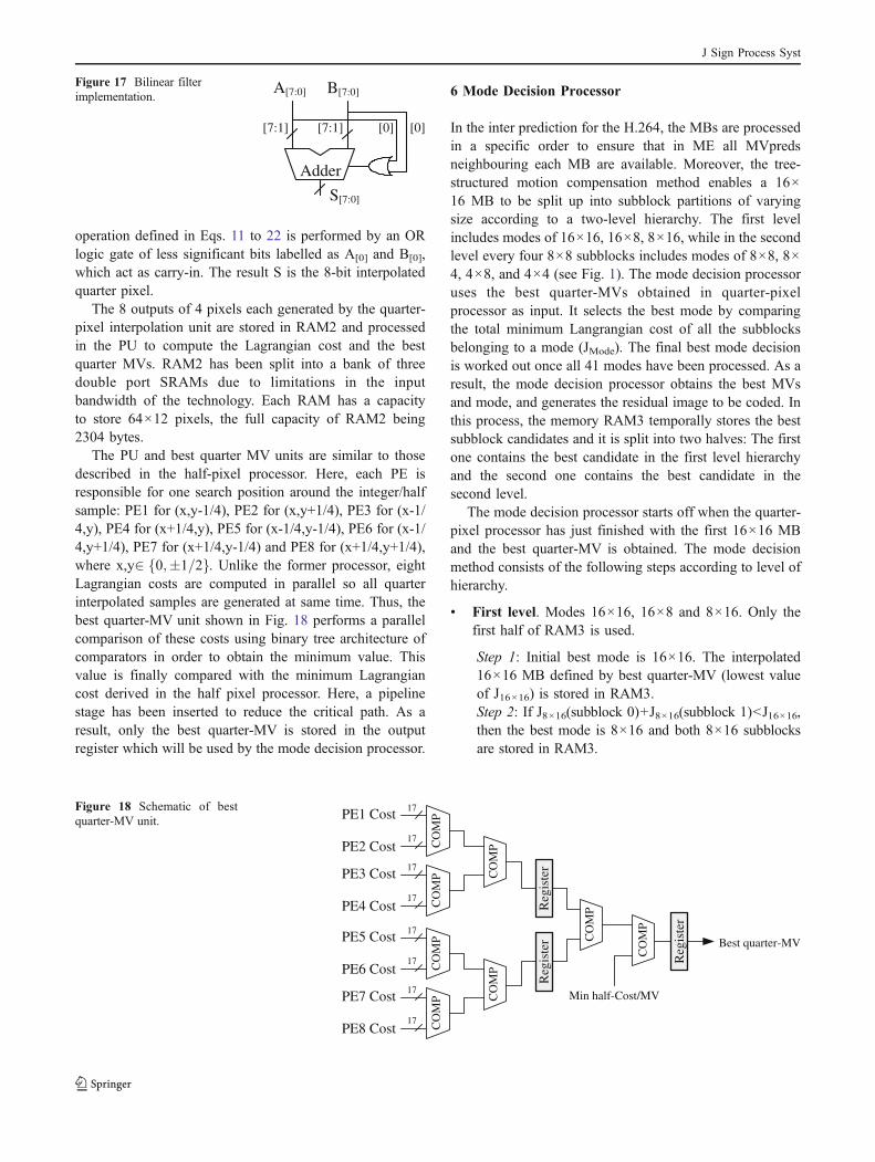
The Best half-MV unit finds the best half-MV by searchingfor the minimum Lagrangian cost generated in PU.Figure 13 shows the schematic of this circuit made up oftwo comparators and a register which stores the minimumLagrangian cost and its corresponding best half MV. Thisregister is initialized by the data from the IME with theLagrangian cost and MV for the best integer position. TheBest half-MV unit processes in parallel two Lagrangiancosts generated in the PU; to maintain the regularity, thecost of PE3 is delayed 1 clock cycle to coincide in timewith the cost of PE4. The register stores new data whether aminimum Lagrangian cost is found or not. This processfinishes when all Lagrangian costs are compared. As aresult, the data stored in the register, Lagrangian cost andhalf-MV, are passed to the quarter-pixel processor.
4.4 RAM1 Memory
A good compromise between the memory usage andcomputational complexity is to interpolate the half-pixelvalues and to store all of them in a memory to be computedin the quarter processor when they are needed. In RAM1the pixel values {I}, {H}, {V} and {D} generated in thehalf-pixel interpolation unit are stored in a bank of fourdouble port RAMs. For the sake of clarity, Fig. 14 showsthe distribution in RAM1 of pixels for a 4×4 subblock. Thewhite core contains the pixels used in the half-pixelprocessor and the pixels in the grey frame are only usedby the bilinear filters in the quarter interpolation. Tosimplify the quarter interpolation, the pixels are storedrow by row using words of 6 pixels for {I} and {V} andwords of 5 pixels for {H} and {D}. Thus, RAM1 must beable to store the interpolated pixels for a 16×16 block. Inthis case, the block is split up in 4 rows of 16+1+1 elementseach for {I} and {H}, which implies 18×4×6 bytes for {I}and 18×4×5 bytes for {H}. The number of elements for{V} and {D} in each row is lower resulting in 17×4×6bytes for {V} and 17×4×5 bytes for {D}. The total size ofRAM1 is 1540 bytes.
Adder8
S3
Adder
Ri,38
Ci,38
8
S2
Ri,28
Ci,28
Adder8
S1
Ri,18
Ci,18
Adder8
S0
Ri,08
Ci,08
9Adder
9RegReg Reg
Adder
Adder
10
MUX
Langragian Cost
Reg
12λΜVcost
17
Absolute difference
Adder tree
Adder accumulator
Reg
init
Adder
Figure 11 Processing element (PE) circuit.
J Sign Process Syst

5 Quarter-Pixel Processor
The quarter-pixel processor performs quarter -pixel inter-polation and a quarter-pixel search for each subblock size.Once the best half-pixel search is completed, the quarterpixel values are computed around it by bilinear filtersaccording to the scheme shown in Fig. 15. Here, quarterpixels are indicated in circles and half and integer pixels insquares. The half-pixel processor selects 1 out of 9 possible
options: D−1,−1, V−1,0, D−1,0, H0,−1, I0,0, H0,0, D0,−1, V0,0
and D0,0. Thus, only 8 quarter pixels around the best half-pixel selection must be interpolated into quarter-pixelresolution.
17PEi Cost
17 CO
MP
Min Cost/MV
Reg
iste
r
Min Cost/Best half-MV
CO
MP
PEj Cost MU
X
Minimum integer Lagrangian cost/MV
init
Figure 13 Schematic of best half-MV unit.
{I} {H} {V} {D}Figure 14 Distribution of pixels in RAM1 for a 4×4 subblock.
Figure 12 Data flow scheduleof PU for a 4×4 subblock:a) Half-pixel interpolation,b) timing diagram.
J Sign Process Syst

In the grey box in Fig. 15, twelve different types ofquarter pixels are highlighted, classified as horizontal {ha,hb, hc, hd}, vertical {va, vb, vc, vd} and diagonal {da, db,dc, dd}, according to the direction used in their generationfrom half and integer pixels. The four quarter pixels in thehorizontal direction are defined as
ha0;0 ¼ I0;0 þ H0;0 þ 1� �
>> 1 ð11Þ
hb0;0 ¼ H0;0 þ I0;1 þ 1� �
>> 1 ð12Þ
hc0;0 ¼ V0;0 þ D0;0 þ 1� �
>> 1 ð13Þ
hd0;0 ¼ D0;0 þ V0;1 þ 1� �
>> 1 ð14ÞThe four quarter-pixel values in the vertical direction are
defined as
va0;0 ¼ I0;0 þ V0;0 þ 1� �
>> 1 ð15Þ
vb0;0 ¼ H0;0 þ D0;0 þ 1� �
>> 1 ð16Þ
vc0;0 ¼ V0;0 þ I1;0 þ 1� �
>> 1 ð17Þ
vd0;0 ¼ D0;0 þ H1;0 þ 1� �
>> 1 ð18Þ
Finally, the four quarter-pixel values in the diagonaldirection are defined as
da0;0 ¼ H0;0 þ V0;0 þ 1� �
>> 1 ð19Þ
db0;0 ¼ H0;0 þ V0;1 þ 1� �
>> 1 ð20Þ
dc0;0 ¼ V0;0 þ H1;0 þ 1� �
>> 1 ð21Þ
dd0;0 ¼ V0;1 þ H1;0 þ 1� �
>> 1 ð22ÞFigure 16 illustrates the scheme of the quarter-pixel
interpolation unit. During each clock cycle, 22 input pixels{I}, {H}, {V} and {D} are read in parallel from RAM1 rowby row in vertical order, which are selected according tobest half-pixel MVs. If the best half-pixel is {V} or {D},then two adjacent rows of {I} and {H} samples arenecessary to perform the quarter-pixel interpolation. Other-wise, if the best half-pixel is {I} or {H} then two adjacentrows of {V} and {D} samples are used. Two multiplexersperform this kind of selection, storing the two adjacentrows in registers REG1 and REG2 and the best half-pixel inREG3. The 33 pixels of these registers run into the bilinearfilter array arranged in 8 blocks of 4 basic elementsbelonging to the same type of quarter pixel. Each basicbilinear filter is implemented by means of the optimizedscheme of Fig. 17 where a 7-bit adder is used instead of the8-bit adder used in a classic implementation. The rounding
I0,0
V0,0
H0,0
D0,0
I1,0 H1,0
V0,1
I0,1
I1,1
ha0,0 hb0,0
va0,0 vb0,0 va0,1da0,0 db0,0
hc0,0 hd0,0
vc0,0 vd0,0dc0,0 dd0,0
ha1,0 hb1,0
vc0,1
H0,-1
D0,-1
hb0,-1
vb0,-1 db0,-1
hd0,-1
vc-1,0 vd-1,0 vc-1,0dc-1,0 dd-1,0vd-1,-1 dd-1,-1
V-1,0 D-1,0 V1,1hc-1,0 hd-1,0D-1,-1 hd-1,-1
H1,-1
vd0,-1 dd0,-1
hb1,-1
va-1,0 vb-1,0 va-1,1da-1,0 db-1,0vb-1,-1 db-1,-1
I-1,0 H0,0 I-1,1ha-1,0 hb-1,0H0,-1 hb-1,-1
I0,-1
V0,-1
I1,-1
ha0,-1
va0,-1 da0,-1
hc0,-1
vc0,-1 dc0,-1
ha1,-1
vc-1,-1 dc-1,-1
V-1,-1 hc-1,-1
va-1,-1 da-1,-1
I-1,-1 ha-1,-1
Figure 15 Interpolation of quarter-pixel samples (shown in circles)by bi-linear filters centred around integer sample I0,0.
H
REG 1
REG 2
REG 3
MUXMUX{I},{H}
or{D},{V}
I DV
RAM1
Bilinearfilter array
6 5 6 5
11 11 11
Interpolated quarter pixels
4 4 4 4 4 4 4 4
BF 1 BF 2 BF 3 BF 4 BF 5 BF 6 BF 7 BF 8
Figure 16 Architecture of quarter-pixel interpolator unit.
J Sign Process Syst
operation defined in Eqs. 11 to 22 is performed by an ORlogic gate of less significant bits labelled as A[0] and B[0],which act as carry-in. The result S is the 8-bit interpolatedquarter pixel.
The 8 outputs of 4 pixels each generated by the quarter-pixel interpolation unit are stored in RAM2 and processedin the PU to compute the Lagrangian cost and the bestquarter MVs. RAM2 has been split into a bank of threedouble port SRAMs due to limitations in the inputbandwidth of the technology. Each RAM has a capacityto store 64×12 pixels, the full capacity of RAM2 being2304 bytes.
The PU and best quarter MV units are similar to thosedescribed in the half-pixel processor. Here, each PE isresponsible for one search position around the integer/halfsample: PE1 for (x,y-1/4), PE2 for (x,y+1/4), PE3 for (x-1/4,y), PE4 for (x+1/4,y), PE5 for (x-1/4,y-1/4), PE6 for (x-1/4,y+1/4), PE7 for (x+1/4,y-1/4) and PE8 for (x+1/4,y+1/4),where x,y2 0;�1=2f g. Unlike the former processor, eightLagrangian costs are computed in parallel so all quarterinterpolated samples are generated at same time. Thus, thebest quarter-MV unit shown in Fig. 18 performs a parallelcomparison of these costs using binary tree architecture ofcomparators in order to obtain the minimum value. Thisvalue is finally compared with the minimum Lagrangiancost derived in the half pixel processor. Here, a pipelinestage has been inserted to reduce the critical path. As aresult, only the best quarter-MV is stored in the outputregister which will be used by the mode decision processor.
6 Mode Decision Processor
In the inter prediction for the H.264, the MBs are processedin a specific order to ensure that in ME all MVpredsneighbouring each MB are available. Moreover, the tree-structured motion compensation method enables a 16×16 MB to be split up into subblock partitions of varyingsize according to a two-level hierarchy. The first levelincludes modes of 16×16, 16×8, 8×16, while in the secondlevel every four 8×8 subblocks includes modes of 8×8, 8×4, 4×8, and 4×4 (see Fig. 1). The mode decision processoruses the best quarter-MVs obtained in quarter-pixelprocessor as input. It selects the best mode by comparingthe total minimum Langrangian cost of all the subblocksbelonging to a mode (JMode). The final best mode decisionis worked out once all 41 modes have been processed. As aresult, the mode decision processor obtains the best MVsand mode, and generates the residual image to be coded. Inthis process, the memory RAM3 temporally stores the bestsubblock candidates and it is split into two halves: The firstone contains the best candidate in the first level hierarchyand the second one contains the best candidate in thesecond level.
The mode decision processor starts off when the quarter-pixel processor has just finished with the first 16×16 MBand the best quarter-MV is obtained. The mode decisionmethod consists of the following steps according to level ofhierarchy.
& First level. Modes 16×16, 16×8 and 8×16. Only thefirst half of RAM3 is used.
Step 1: Initial best mode is 16×16. The interpolated16×16 MB defined by best quarter-MV (lowest valueof J16×16) is stored in RAM3.Step 2: If J8×16(subblock 0)+J8×16(subblock 1)<J16×16,then the best mode is 8×16 and both 8×16 subblocksare stored in RAM3.
Adder
A[7:0] B[7:0]
[7:1] [7:1] [0] [0]
S[7:0]
Figure 17 Bilinear filterimplementation.
17PE1 Cost
17
Best quarter-MV
CO
MP
PE2 Cost
Min half-Cost/MV
17PE3 Cost
17PE4 Cost
17PE5 Cost
17PE6 Cost
17PE7 Cost
17PE8 Cost
CO
MP
CO
MP
CO
MP
CO
MP
CO
MP
CO
MP
CO
MP
Reg
iste
r
Reg
iste
rR
egis
ter
Figure 18 Schematic of bestquarter-MV unit.
J Sign Process Syst

Step 3: If J16×8(0)+J16×8(1)<J(best mode step 2), then thebest mode is 16×8 and both 16×8 subblocks are storedin RAM3.
& Second level. Modes 8×8, 8×4, 4×8, and 4×4.Repeated for each four 8×8 subblocks. Only the secondhalf of RAM3 is used, which is split into four parts eachone managed by an 8×8 subblock.
Step 4: The initial best mode is 8×8. The interpolated8×8 subblock defined by the best quarter-MV (lowestvalue of J8×8) is stored in RAM3.Step 5: If J4×8(0)+J4×8(1)<J8×8, then the best mode is4×8 and both 4×8 subblocks are stored in RAM3.Step 6: If J8×4(0)+J8×4(1)<J(best mode step 5), then thebest mode is 8×4 and both 8×4 subblocks are stored inRAM3.Step 7: If J4×4(0)+J4×4(1)+J4×4(3)+J4×4(4)<J(best mode
step 6), then the best mode is 4×4 and all 4×4 subblocksare stored in RAM3.
& Final decision. The best mode for candidates in firstand second level are compared searching for theminimum JMode, then the best mode and MVs are
found. The residual image is computed by substractingthe best interpolated image and the current image.
7 Implementation Results
The proposed FME architecture has been designed aiming forregular flow and efficient hardware utilization. This circuithas been implemented in Verilog VHDL at RTL level and ithas been synthesized using a TSMC 180 nm CMOS library.The final layout is shown is Fig. 19 and its area is 1.2×1.1 mm2. It uses 11.4 k gates and a total of 4356 Bytes indifferent RAMs. In typical working conditions (1.8 V, 25°C),the maximum frequency of 290 MHz can be achievedincluding wire delays. It takes a total of 870 clock cycles(832 for input data and 38 of latency) to process a MB and anadditional 66 clock cycles to generate the residual image. Itcan provide enough processing capacity for 1920×1088@30fps real-time video streams.
Table 2 shows the hardware comparison of the FMEdesigns implemented in a similar technology. Our designgenerates the residual image and the best MVs with a highthroughput and low area cost architecture. Part of thishardware reduction is achieved using SAD as a distortionmeasure instead of the sum of absolute transformed differ-ences (SATD) implemented in [16–18, 20]. The designs[16, 20] and ours use the same input bandwidth of 10pixels. However, our design roughly multiplies by three theoperating frequency and the reduction of latency is enoughto process 1080p@30fps videos. In [17], the inputbandwidth is increased to 22 pixels to remove all theredundant columns by adopting a 16-pixel interpolationunit. It operates at the same frequency as ours with a slightreduction in latency and a bigger area cost (2.7 mm2 incomparison with 1.32 mm2). Moreover, it does not explainwhether the best interpolated MB is stored or not. A verydifferent scheme is used in the design presented in [18]which is focused on low hardware cost but with a greatlatency. Finally, the three-engine architecture [19] operatesat 150 MHz and it takes 616 clock cycles to process a MB.
RAM1
RAM2
RAM3RAM3
Figure 19 Lay-out of proposed FME with Faraday 180 nm CMOStechnology.
Ref. [16] [17] [18] [20] [19] Ours
Tech. (µm) UMC 0.18 TSMC 0.18 TSMC 0.18 UMC 0.18 TSMC 0.13 UMC 0.18
Freq. (MHz) 100 285 274 100 150 290
Gate Count 79 k 188 k 24 k 48 k 188 k 11.4 k
RAM No No 1904 bits No 9724 Bytes 4356 Bytes
Area (mm2) NA 1.8×1.5 0.58×0.66 NA NA 1.2×1.1
Resolution 720×576 1920×1088 NA 720×576 1920×1088 1920×1088
Input pixels 10 22 1 10 NA 10
Latency 1648 790 39551 2000 616 870
Table 2 Comparison of theFME with other designs.
J Sign Process Syst

Each engine processes different kinds of subblocks in apipelined way to increase throughput. However, it requiresmore gates and RAM than ours and its area is much biggereven using a better technology.
8 Conclusions
In this paper, we propose a high performance VLSIarchitecture for FME in H.264/AVC with enough process-ing capacity for 1080HD real-time video streams. This archi-tecture is made up of three different pipelined processorsto provide a trade-off between processing time and hard-ware utilization. These processors implement a completelystandard-compatible full-search algorithm and are capableof processing a macroblock (MB) in 870 clock cycles using4-pixel interpolation units with a 10-pixel input bandwidth ofreference pixels. Our design is implemented with only 11.4 kgates and 4.4kBytes of RAM in a standard 180 nm CMOStechnology at an operating frequency of 290 MHz. Com-pared with previous works, it presents a high throughput andlow area cost architecture, which can generate the residualimage and the best MVs ready to be encoded.
Acknowledgment We wish to acknowledge the Spanish Ministry ofEducation and Science for the financial help TEC2006-12438/TCMreceived to support this work.
References
1. Ostermann, J., Bormans, J., List, P., Marpe, D., Narroschke, M.,Pereira, F., et al. (2004). Video coding with H.264/AVC: tools,performance, and complexity. IEEE Circuits and Systems Maga-zine, 4(1), 7–28. First Quarter.
2. Wiegand, T., Sullivan, G. J., Bjontegaard, G., & Luthra, A.(2003). Overview of H.264/AVC video coding standard. IEEETransactions on Circuits and Systems for Video Technology, 13(7), 560–576.
3. ITU-T Rec. H.264/ISO/IEC 11496-10 (2003). Advanced VideoCoding. Final Committee Draft, Document JVTG050.
4. Online document. http://iphome.hhi.de/suehring/tml/. Accessed 17September 2009.
5. Yap, S. Y., & McCanny, J. V. (1989). A VLSI architecture forvariable block size video motion estimation. IEEE Transactionson Circuits and Systems for Video Technology, 36(2), 1301–1308.
6. Komarek, T., & Pirsh, P. (2006). Array architectures for blockmatching algorithms. IEEE Transactions on Circuits and Systemsfor Video Technology, 16(7), 876–883.
7. Jong, H. M., Chen, L. G., & Chiueh, T. D. (1994). Parallelarchitecture for 3-step hierarchical search block-matching algo-rithm. IEEE Transactions on Circuits and Systems for VideoTechnology, 4(4), 407–416.
8. Zhu, C., Lin, X., & Chau, L. P. (2002). Hexagon-based searchpattern for fast block motion estimation. IEEE Transactions onCircuits and Systems for Video Technology, 12(5), 349–355.
9. Zhu, C., & Ma, K. K. (2000). A new diamond search algorithm,for fast block matching motion estimation. IEEE Transactions onImage Processing, 9(2), 287–290.
10. Chen, T. C., Chen, Y. H., Tsai, S. F., Chien, S. I., & Chen, L. G.(2007). Fast algorithm and architecture design of low-powerinteger motion estimation for H.264/AVC. IEEE Transactions onCircuits and Systems for Video Technology, 17(5), 568–577.
11. Li, D. X., & Zhang, M. (2007). Architecture design for H.264/AVCinteger motion estimation with minimum memory bandwidth. IEEETransactions on Consumer Electronics, 53(3), 1053–1060.
12. Zhenyu, W., Baochen, J., Xudong, Z., & Yu, C. (2004). A newfull-pixel and sub-pixel motion vector search algorithm for fastblock-matching motion estimation in H.264. Proceedings of theThird International Conference on Image and Graphics, 345–348.
13. La, B., Eom, M., & Choe, Y. (2007). Fast sub-pixel search controlby using neighbour motion vector in H.264. 9th InternationalConference on Advanced Communication Technology, 1, 62–65.
14. Hyun, C. J., Kim, S. D., & Sunwoo, M. H. (2006). Efficientmemory reuse and sub-pixel interpolation algorithms for ME/MCof H.264/AVC. IEEE Workshop on Signal Processing SystemsDesign and Implementation, 377–382. October.
15. Song, Y., Ma, Y., Liu, Z., Ikenaga, T., & Goto, S. (2008).Hardware-oriented direction-based fast fractional motion estima-tion algorithm in H.264/AVC. IEEE International Conference onMultimedia and Expo, 1009–1012, June.
16. Chen, T. C., Huang, Y. W., & Chen, L. G. (2004). Fully utilizedand reusable architecture for fractional motion estimation ofH.264/AVC. IEEE International Conference on Acoustics,Speech, and Signal Processing, 5, 9–12.
17. Yang, C., Goto, S., Ikenaga, T. (2006). High performance VLSIarchitecture of fractional motion estimation in H.264 for HDTV.IEEE International Symposium on Circuits and Systems, 2605–2608.
18. Song, Y., Liu, Z., Goto, S., & Ikenaga, T. (2005). A VLSIarchitecture for Motion compensation interpolation in H.264/AVC. 6th International Conference on ASIC, 279–282. October.
19. Wu, C. L., Kao, C. Y., & Lin, Y. L. (2008). A high performancethree-engine architecture for H.264/AVC fractional motion esti-mation. IEEE International Conference on Multimedia and Expo,133–136.
20. Wang, Y. J., Cheng, C. C., & Chang, T. S. (2007). A fast algorithmand its VLSI architecture for fractional motion estimation forH.264/MPEG-4 AVC video coding. IEEE Transactions on Circuitsand Systems for Video Technology, 17(5), 578–583.
21. Lin, Y. K., Lin, C. C., Kuo, T. Y., & Chang, T. S. (2008). Ahardware-efficient H.264/AVC motion-estimation design for high-definition video. IEEE Transactions on Circuits and Systems, 55(6), 1526–1535.
22. Yalcin, S., & Hamzaoglu, I. (2006). A high performance hardwarearchitecture for half-pixel accurate H.264 motion estimation. IFIPInternational Conference on Very Large Scale Integration, 63–67.October.
23. Rahman, C. A. & Badawy, W. (2005). A quarter pel full searchblock motion estimation architecture for H.264/AVC. IEEEInternational Conference on Multimedia and Expo, 414–417. July.
24. Chen, T. C., Chien, S. Y., Huang, Y. W., Tsai, C. H., Chen, C. Y.,Chen, T. W., et al. (2006). Analysis and architecture design of anHDTV720p 30 frames/s H.264/AVC encoder. IEEE Transactionson Circuits and Systems for Video Technology, 16(6), 673–688.
25. Huang, Y. W., Chen, T. C., Tsai, C. H., Chen, C. Y., Chen, T. W.,Chen, C. S., et al. (2005). A 1.3TOPS H.264/AVC Single-ChipEncoder for HDTV Applications. ISSCC Digest of TechnicalPaper, 128–129. February.
26. Sihvo, T., & Niittylahti, J. (2005). H.264/AVC interpolationoptimization. IEEE Workshop on Signal Processing SystemsDesign and Implementation, 307–312. November.
27. Vanne, J., Ahn, E., Hämäläinen, T. D., & Kuusilinna, K. (2006). Ahigh-performance sum of absolute difference implementation formotion estimation. IEEE Transactions on Circuits and Systems forVideo Technology, 16(7), 876–883.
J Sign Process Syst

Gustavo A. Ruiz was born in Burgos, Spain, in 1962. He received theM.Sc. degree in physics in 1985 from the University of Navarra,Spain, and the Ph.D. degree in physical science in 1989 from theUniversity of Cantabria, Santander, Spain. Since 1985, he has beenwith the Department of Electronics and Computers at the University ofCantabria, where he is currently an Associate Professor. His currentresearch interests are mainly focused on VLSI architectures for signalprocessing and high-speed arithmetic circuits.
Juan A. Michell was born in Cáceres, Spain, in 1952. He received theM.S. and the Ph.D. degrees in physical sciences from the Universityof Cantabria, Spain, in 1974 and 1977, respectively. Since 1974 he hasbeen with the Department of Electronics and Computers at theUniversity of Cantabria, where he was appointed Professor inElectronics in 1991. His current research interests are VLSIarchitectures and integrated circuit design for digital signal processingapplications.
J Sign Process Syst