Embed Size (px)
Citation preview
ISSN No: 2348-4845
Volume No: 2 (2015), Issue No: 7 (July) July 2015 www.ijmetmr.com Page 599
International Journal & Magazine of Engineering, Technology, Management and Research
A Peer Reviewed Open Access International Journal
The efforts put by Jagadguru Swami Sri Bharati Krishna Tirtha Maharaja to introduce Vedic Mathematics to the commoners as well as streamline Vedic Algorithms into 16 categories [1] or Sutras needs to be acknowledged and appreciated. The Urdhva Tiryakbhayam is one such multiplication algorithm which is well known for its ef-ficiency in reducing the calculations involved. With the advancement in the VLSI technology, there is an ever increasing quench for portable and embedded Digital Signal Processing (DSP) systems. DSP is omnipresent in almost every engineering discipline. The paper is or-ganized as follows: The section II gives the basics of re-versible logic along with the literature review. Section III explains the Urdhva Tiryakbhayam algorithm. The section IV describes the modifications of the previous design in order to evolve the optimized design. Section V compares the proposed design with the other non Vedic multipliers as well as the previous Vedic multipli-er design and draws a conclusion claiming the versatil-ity of Reversible Urdhva Tiryakbhayam multiplier.
REVERSIBLE LOGIC:
A. Literature Survey and Significance of reversible logic Conventional combinational logic circuits are known to dissipate heat for every bit of information that is lost. This is also evident from the second law of thermody-namics which states that any irreversible process leads to loss of energy. Landauer [3] showed that any gate that is irreversible, necessarily dissipates energy, and each irreversible bit generates k*T ln2 joules of heat where k is Boltzmann’s constant (1.38 x 10⁻²³ joules/Kelvin) and T is temperature in Kelvin. Lowering the threshold voltage and management of the power sup-ply are widely applied practices to decrease the energy consumption in any logical operation [23].
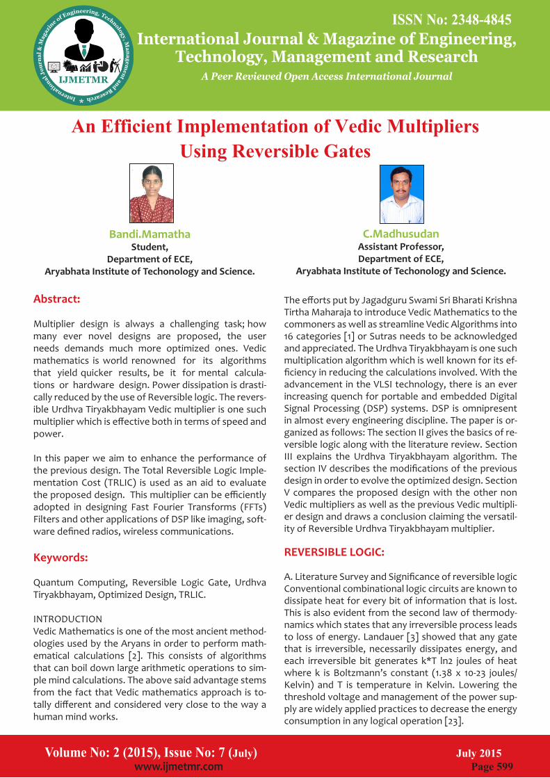
Abstract:
Multiplier design is always a challenging task; how many ever novel designs are proposed, the user needs demands much more optimized ones. Vedic mathematics is world renowned for its algorithms that yield quicker results, be it for mental calcula-tions or hardware design. Power dissipation is drasti-cally reduced by the use of Reversible logic. The revers-ible Urdhva Tiryakbhayam Vedic multiplier is one such multiplier which is effective both in terms of speed and power.
In this paper we aim to enhance the performance of the previous design. The Total Reversible Logic Imple-mentation Cost (TRLIC) is used as an aid to evaluate the proposed design. This multiplier can be efficiently adopted in designing Fast Fourier Transforms (FFTs) Filters and other applications of DSP like imaging, soft-ware defined radios, wireless communications.
Keywords:
Quantum Computing, Reversible Logic Gate, Urdhva Tiryakbhayam, Optimized Design, TRLIC.
INTRODUCTIONVedic Mathematics is one of the most ancient method-ologies used by the Aryans in order to perform math-ematical calculations [2]. This consists of algorithms that can boil down large arithmetic operations to sim-ple mind calculations. The above said advantage stems from the fact that Vedic mathematics approach is to-tally different and considered very close to the way a human mind works.
Bandi.MamathaStudent,
Department of ECE,Aryabhata Institute of Techonology and Science.
C.MadhusudanAssistant Professor,Department of ECE,
Aryabhata Institute of Techonology and Science.
An Efficient Implementation of Vedic Multipliers Using Reversible Gates
ISSN No: 2348-4845
Volume No: 2 (2015), Issue No: 7 (July) July 2015 www.ijmetmr.com Page 600
International Journal & Magazine of Engineering, Technology, Management and Research
A Peer Reviewed Open Access International Journal
• Flexibility: This refers to the universality of a revers-ible logic gate in realizing more functions.
• Quantum cost (QC): This refers to the cost of the cir-cuit in terms of the cost of a primitive gate. It is calcu-lated knowing the number of primitive reversible logic gates (1x1 or 2x2) required to realize the circuit
• Gate levels: This refers to the number of levels in the circuit which are required to realize the given logic functions.
• Total Reversible Logic Implementation Cost (TRLIC) [12]: Let, in a reversible logic circuit there are NG re-versible logic gates, CI constant inputs, GO number of garbage outputs, and have a quantum cost QC. Then the TRLIC is given as
URDHVA TIRYAKBHAYAM MULTIPLICATION ALGORITHM:
Urdhva Tiryakbhayam (UT) is a multiplier based on Ve-dic mathematical algorithms deviced by ancient Indian Vedic mathematicians. Urdhva Tiryakbhayam sutra can be applied to all cases of multiplications viz. Binary, Hex and also Decimals. It is based on the concept that generation of all partial products can be done and then concurrent addition of these partial products is per-formed.
The parallelism in generation of partial products and their summation is obtained using Urdhva Tiryak-bhayam. Unlike other multipliers with the increase in the number of bits of multiplicand and/or multiplier the time delay in computation of the product does not in-crease proportionately. Because of this fact the time of computation is independent of clock frequency of the processor. Hence one can limit the clock frequency to a lower value. Also, since processors using lower clock frequency dissipate lower energy., it is economical in terms of power factor to use low frequency processors employing fast algorithms like the above mentioned.
The Multiplier based on this sutra has the advantage that as the number of bits increases, gate delay and area increases at a slow pace as compared to other conventional multipliers. The Algorithm: Multiplication of 101 by 110.
However these technologies of lowering the energy consumption will hit a barrier of kT [24]. In order to al-leviate this, techniques such as reducing the tempera-ture of computer and constructing a thermodynami-cally reversible computer can be used [25].
REVERSIBLE LOGIC GATES:
A Reversible Logic gate is an n-input n-output logic func-tion in which there is a one-to-one correspondence be-tween the inputs and the outputs. This not only helps to determine the outputs from the inputs but also the inputs can be uniquely recovered from the outputs. Because of this bijective mapping the output vectors are merely permutations of the input vectors.Some of the basic reversible logic gates in the literature those are useful in designing the Reversible Urdhva Tiryak-bhayam Multiplier are shown in the figure.
Figure: reversible logic gatesOptimization parameters for reversible logic circuits: The important parameters which play a major role in the design of an optimized reversible logic circuit are as listed:
• Constants (CI): This refers to the number of inputs that are to be maintained constant at either 0 or 1 in order to synthesize the given logical function.
• Garbage (GO): This refers to the number of outputs which are not used in the synthesis of a given function. These are very essential, without which reversibility cannot be achieved.
• Gate count (NG): The number of reversible gates used to realize the function.
ISSN No: 2348-4845 ISSN No: 2348-4845
Volume No: 2 (2015), Issue No: 7 (July) July 2015 www.ijmetmr.com Page 601
International Journal & Magazine of Engineering, Technology, Management and Research
A Peer Reviewed Open Access International Journal
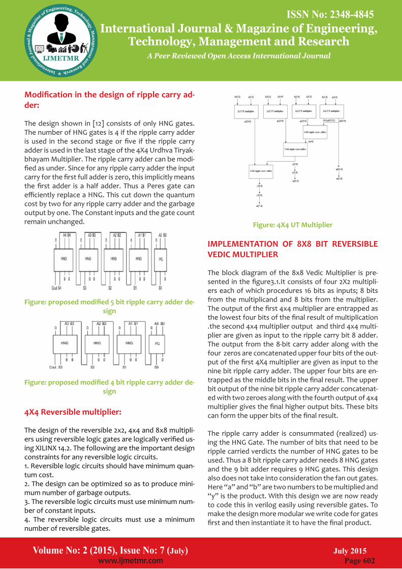
Figure: conventional 2x2 urdhva tiryakbhayam multi-plier
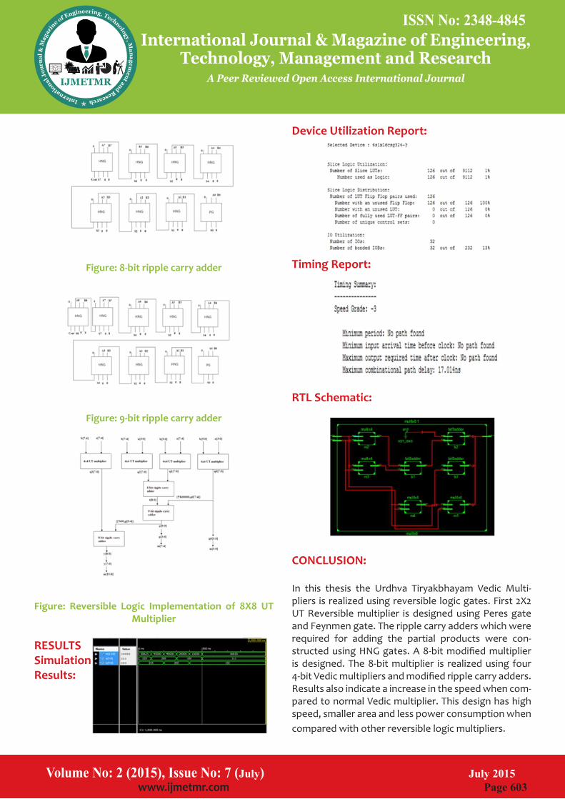
Figure: Reversible 2x2 UT multiplier
Design of 4x4 Urdhva Tiryakbhayam Revers-ible multiplier:
The Reversible 4X4 Urdhva Tiryakbhayam Multiplier design emanates from the 2X2 multiplier. The block diagram of the 4X4 Vedic Multiplier is presented in the figure 6. It consists of four 2X2 multipliers each of which procures four bits as inputs; two bits from the multiplicand and two bits from the multiplier. The low-er two bits of the output of the first 2X2 multiplier are entrapped as the lowest two bits of the final result of multiplication. Two zeros are concatenated with the upper two bits and given as input to the four bit ripple carry adder. The other four input bits for the ripple car-ry adder are obtained from the second 2X2 multiplier.Likewise the outputs of the third and the terminal 2X2 multipliers are given as inputs to the second four bit ripple carry adder. The outputs of these four bit ripple carry adders are in turn 5 bits each which need to be summed up. This is done by a five bit ripple carry ad-der which generates a six bit output. These six bits can form the upper bits of the final result.
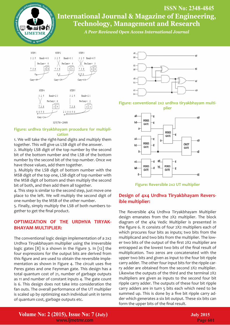
Figure: urdhva tiryakbhayam procedure for multipli-cation
1. We will take the right-hand digits and multiply them together. This will give us LSB digit of the answer.2. Multiply LSB digit of the top number by the second bit of the bottom number and the LSB of the bottom number by the second bit of the top number. Once we have those values, add them together.3. Multiply the LSB digit of bottom number with the MSB digit of the top one, LSB digit of top number with the MSB digit of bottom and then multiply the second bit of both, and then add them all together.4. This step is similar to the second step, just move one place to the left. We will multiply the second digit of one number by the MSB of the other number.5. Finally, simply multiply the LSB of both numbers to-gether to get the final product.
OPTIMIZATION OF THE URDHVA TIRYAK-BHAYAM MULTIPLIER:
The conventional logic design implementation of a 2x2 Urdhva Tiryakbhayam multiplier using the irreversible logic gates [8] is a shown in the Figure 3. In [12] the four expressions for the output bits are derived from this figure and are used to obtain the reversible imple-mentation as shown in Figure 4. The circuit uses five Peres gates and one Feynman gate. This design has a total quantum cost of 21, number of garbage outputs as 11 and number of constant inputs 4. The gate count is 6. This design does not take into consideration the fan outs. The overall performance of the UT multiplier is scaled up by optimizing each individual unit in terms of quantum cost, garbage outputs etc.
Volume No: 2 (2015), Issue No: 7 (July) July 2015 www.ijmetmr.com Page 602
International Journal & Magazine of Engineering, Technology, Management and Research
A Peer Reviewed Open Access International Journal
Figure: 4X4 UT Multiplier
IMPLEMENTATION OF 8X8 BIT REVERSIBLE VEDIC MULTIPLIER
The block diagram of the 8x8 Vedic Multiplier is pre-sented in the figure3.1.It consists of four 2X2 multipli-ers each of which procedures 16 bits as inputs; 8 bits from the multiplicand and 8 bits from the multiplier. The output of the first 4x4 multiplier are entrapped as the lowest four bits of the final result of multiplication .the second 4x4 multiplier output and third 4x4 multi-plier are given as input to the ripple carry bit 8 adder. The output from the 8-bit carry adder along with the four zeros are concatenated upper four bits of the out-put of the first 4X4 multiplier are given as input to the nine bit ripple carry adder. The upper four bits are en-trapped as the middle bits in the final result. The upper bit output of the nine bit ripple carry adder concatenat-ed with two zeroes along with the fourth output of 4x4 multiplier gives the final higher output bits. These bits can form the upper bits of the final result.
The ripple carry adder is consummated (realized) us-ing the HNG Gate. The number of bits that need to be ripple carried verdicts the number of HNG gates to be used. Thus a 8 bit ripple carry adder needs 8 HNG gates and the 9 bit adder requires 9 HNG gates. This design also does not take into consideration the fan out gates. Here “a” and “b” are two numbers to be multiplied and “y” is the product. With this design we are now ready to code this in verilog easily using reversible gates. To make the design more modular we write code for gates first and then instantiate it to have the final product.
Modification in the design of ripple carry ad-der:
The design shown in [12] consists of only HNG gates. The number of HNG gates is 4 if the ripple carry adder is used in the second stage or five if the ripple carry adder is used in the last stage of the 4X4 Urdhva Tiryak-bhayam Multiplier. The ripple carry adder can be modi-fied as under. Since for any ripple carry adder the input carry for the first full adder is zero, this implicitly means the first adder is a half adder. Thus a Peres gate can efficiently replace a HNG. This cut down the quantum cost by two for any ripple carry adder and the garbage output by one. The Constant inputs and the gate count remain unchanged.
Figure: proposed modified 5 bit ripple carry adder de-
sign
Figure: proposed modified 4 bit ripple carry adder de-sign
4X4 Reversible multiplier:
The design of the reversible 2x2, 4x4 and 8x8 multipli-ers using reversible logic gates are logically verified us-ing XILINX 14.2. The following are the important design constraints for any reversible logic circuits.1. Reversible logic circuits should have minimum quan-tum cost.2. The design can be optimized so as to produce mini-mum number of garbage outputs.3. The reversible logic circuits must use minimum num-ber of constant inputs.4. The reversible logic circuits must use a minimum number of reversible gates.
ISSN No: 2348-4845 ISSN No: 2348-4845
Volume No: 2 (2015), Issue No: 7 (July) July 2015 www.ijmetmr.com Page 601
International Journal & Magazine of Engineering, Technology, Management and Research
A Peer Reviewed Open Access International Journal
Figure: conventional 2x2 urdhva tiryakbhayam multi-plier
Figure: Reversible 2x2 UT multiplier
Design of 4x4 Urdhva Tiryakbhayam Revers-ible multiplier:
The Reversible 4X4 Urdhva Tiryakbhayam Multiplier design emanates from the 2X2 multiplier. The block diagram of the 4X4 Vedic Multiplier is presented in the figure 6. It consists of four 2X2 multipliers each of which procures four bits as inputs; two bits from the multiplicand and two bits from the multiplier. The low-er two bits of the output of the first 2X2 multiplier are entrapped as the lowest two bits of the final result of multiplication. Two zeros are concatenated with the upper two bits and given as input to the four bit ripple carry adder. The other four input bits for the ripple car-ry adder are obtained from the second 2X2 multiplier.Likewise the outputs of the third and the terminal 2X2 multipliers are given as inputs to the second four bit ripple carry adder. The outputs of these four bit ripple carry adders are in turn 5 bits each which need to be summed up. This is done by a five bit ripple carry ad-der which generates a six bit output. These six bits can form the upper bits of the final result.
Figure: urdhva tiryakbhayam procedure for multipli-cation
1. We will take the right-hand digits and multiply them together. This will give us LSB digit of the answer.2. Multiply LSB digit of the top number by the second bit of the bottom number and the LSB of the bottom number by the second bit of the top number. Once we have those values, add them together.3. Multiply the LSB digit of bottom number with the MSB digit of the top one, LSB digit of top number with the MSB digit of bottom and then multiply the second bit of both, and then add them all together.4. This step is similar to the second step, just move one place to the left. We will multiply the second digit of one number by the MSB of the other number.5. Finally, simply multiply the LSB of both numbers to-gether to get the final product.
OPTIMIZATION OF THE URDHVA TIRYAK-BHAYAM MULTIPLIER:
The conventional logic design implementation of a 2x2 Urdhva Tiryakbhayam multiplier using the irreversible logic gates [8] is a shown in the Figure 3. In [12] the four expressions for the output bits are derived from this figure and are used to obtain the reversible imple-mentation as shown in Figure 4. The circuit uses five Peres gates and one Feynman gate. This design has a total quantum cost of 21, number of garbage outputs as 11 and number of constant inputs 4. The gate count is 6. This design does not take into consideration the fan outs. The overall performance of the UT multiplier is scaled up by optimizing each individual unit in terms of quantum cost, garbage outputs etc.
Volume No: 2 (2015), Issue No: 7 (July) July 2015 www.ijmetmr.com Page 602
International Journal & Magazine of Engineering, Technology, Management and Research
A Peer Reviewed Open Access International Journal
Figure: 4X4 UT Multiplier
IMPLEMENTATION OF 8X8 BIT REVERSIBLE VEDIC MULTIPLIER
The block diagram of the 8x8 Vedic Multiplier is pre-sented in the figure3.1.It consists of four 2X2 multipli-ers each of which procedures 16 bits as inputs; 8 bits from the multiplicand and 8 bits from the multiplier. The output of the first 4x4 multiplier are entrapped as the lowest four bits of the final result of multiplication .the second 4x4 multiplier output and third 4x4 multi-plier are given as input to the ripple carry bit 8 adder. The output from the 8-bit carry adder along with the four zeros are concatenated upper four bits of the out-put of the first 4X4 multiplier are given as input to the nine bit ripple carry adder. The upper four bits are en-trapped as the middle bits in the final result. The upper bit output of the nine bit ripple carry adder concatenat-ed with two zeroes along with the fourth output of 4x4 multiplier gives the final higher output bits. These bits can form the upper bits of the final result.
The ripple carry adder is consummated (realized) us-ing the HNG Gate. The number of bits that need to be ripple carried verdicts the number of HNG gates to be used. Thus a 8 bit ripple carry adder needs 8 HNG gates and the 9 bit adder requires 9 HNG gates. This design also does not take into consideration the fan out gates. Here “a” and “b” are two numbers to be multiplied and “y” is the product. With this design we are now ready to code this in verilog easily using reversible gates. To make the design more modular we write code for gates first and then instantiate it to have the final product.
Modification in the design of ripple carry ad-der:
The design shown in [12] consists of only HNG gates. The number of HNG gates is 4 if the ripple carry adder is used in the second stage or five if the ripple carry adder is used in the last stage of the 4X4 Urdhva Tiryak-bhayam Multiplier. The ripple carry adder can be modi-fied as under. Since for any ripple carry adder the input carry for the first full adder is zero, this implicitly means the first adder is a half adder. Thus a Peres gate can efficiently replace a HNG. This cut down the quantum cost by two for any ripple carry adder and the garbage output by one. The Constant inputs and the gate count remain unchanged.
Figure: proposed modified 5 bit ripple carry adder de-
sign
Figure: proposed modified 4 bit ripple carry adder de-sign
4X4 Reversible multiplier:
The design of the reversible 2x2, 4x4 and 8x8 multipli-ers using reversible logic gates are logically verified us-ing XILINX 14.2. The following are the important design constraints for any reversible logic circuits.1. Reversible logic circuits should have minimum quan-tum cost.2. The design can be optimized so as to produce mini-mum number of garbage outputs.3. The reversible logic circuits must use minimum num-ber of constant inputs.4. The reversible logic circuits must use a minimum number of reversible gates.
ISSN No: 2348-4845 ISSN No: 2348-4845
Volume No: 2 (2015), Issue No: 7 (July) July 2015 www.ijmetmr.com Page 603
International Journal & Magazine of Engineering, Technology, Management and Research
A Peer Reviewed Open Access International Journal
Device Utilization Report:
Timing Report:
RTL Schematic:
CONCLUSION:
In this thesis the Urdhva Tiryakbhayam Vedic Multi-pliers is realized using reversible logic gates. First 2X2 UT Reversible multiplier is designed using Peres gate and Feynmen gate. The ripple carry adders which were required for adding the partial products were con-structed using HNG gates. A 8-bit modified multiplier is designed. The 8-bit multiplier is realized using four 4-bit Vedic multipliers and modified ripple carry adders. Results also indicate a increase in the speed when com-pared to normal Vedic multiplier. This design has high speed, smaller area and less power consumption when compared with other reversible logic multipliers.
Figure: 8-bit ripple carry adder
Figure: 9-bit ripple carry adder
Figure: Reversible Logic Implementation of 8X8 UT
Multiplier
RESULTSSimulationResults:
Volume No: 2 (2015), Issue No: 7 (July) July 2015 www.ijmetmr.com Page 604
International Journal & Magazine of Engineering, Technology, Management and Research
A Peer Reviewed Open Access International Journal
[5]. Rakshith Saligram and Rakshith T.R. “Design of Reversible Multipliers for linear filtering Applications in DSP” International Journal of VLSI Design and Com-munication systems, Dec-12.
[6]. R. Landauer,”Irreversibility and Heat Generation in the Computational Process”, IBM Journal of Research and Development, 5, pp.183-191, 1961.
[7]. H. Thapliyal and M.B. Srinivas, “Novel Reversible Multiplier Architecture Using Reversible TSG Gate”, Proc.IEEE International Conference on Computer Sys-tems and Applications, pp. 100-103, March 2006.
REFERENCES:
[1]. Jagadguru Swami Sri Bharati Krishna Tirthaji Maha-raja, Vedic Mathematics: Sixteen Simple Mathematical Formulae from the Veda, Delhi (1965).
[2]. H. Thapliyal , M. B. Shrinivas and H. Arbania, ―De-sign and Analysis of a VLSI Based High Performance Low Power Parallel Square Architecture‖, Int. Conf. Algo. Math. Comp. Sc., LasVegas, June 2005, pp. 72-76.
[3]. P. D. Chidgup kar and M. T. Karad, ―The Imp lam-entation of Vedic Algorithms in Digital Signal Process-ing,
[4]. Global J. of Engg. Edu, vol.8, no.2, 2004. Shamim Akhter,VHDL Implementation Of Fast NXN Multipli-er Based On Vedic Mathematics, Jaypee Institute of Information Technology University, Noida, 201307 UP, INDIA, 2007 IEEE.