Embed Size (px)
Citation preview
Future Technology Devices International Ltd (FTDI)
Unit 1, 2 Seaward Place, Centurion Business Park, Glasgow, G41 1HH, United Kingdom
Tel.: +44 (0) 141 429 2777 Fax: + 44 (0) 141 429 2758
E-Mail (Support): [email protected]
Use of FTDI devices in life support and/or safety applications is entirely at the user’s risk, and the user agrees to defend, indemnify and hold harmless FTDI from any and all damages, claims, suits or expense
resulting from such use.
Copyright © 2010 Future Technology Devices International Limited
Future Technology Devices International Ltd.
Vinco Graphics Display Example
Application Note AN_161
Document Reference No.: FT_000363
Version 2.0
Issue Date: 2011-04-15
This application note describes how the Vinco module can be used to display graphics on a LCD display.
`
Copyright © 2010 Future Technology Devices International Limited 1
Document Reference No.: FT_000363
AN_161 Vinco Graphics Display Example
Version 2.0 Clearance No.: FTDI# 190
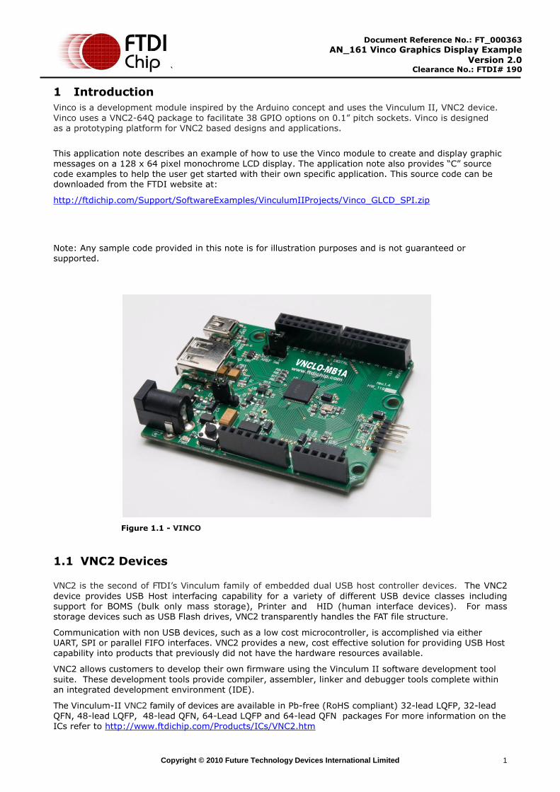
1 Introduction
Vinco is a development module inspired by the Arduino concept and uses the Vinculum II, VNC2 device.
Vinco uses a VNC2-64Q package to facilitate 38 GPIO options on 0.1” pitch sockets. Vinco is designed as a prototyping platform for VNC2 based designs and applications.
This application note describes an example of how to use the Vinco module to create and display graphic messages on a 128 x 64 pixel monochrome LCD display. The application note also provides “C” source code examples to help the user get started with their own specific application. This source code can be downloaded from the FTDI website at:
http://ftdichip.com/Support/SoftwareExamples/VinculumIIProjects/Vinco_GLCD_SPI.zip
Note: Any sample code provided in this note is for illustration purposes and is not guaranteed or
supported.
Figure 1.1 - VINCO
1.1 VNC2 Devices
VNC2 is the second of FTDI’s Vinculum family of embedded dual USB host controller devices. The VNC2
device provides USB Host interfacing capability for a variety of different USB device classes including support for BOMS (bulk only mass storage), Printer and HID (human interface devices). For mass storage devices such as USB Flash drives, VNC2 transparently handles the FAT file structure.
Communication with non USB devices, such as a low cost microcontroller, is accomplished via either UART, SPI or parallel FIFO interfaces. VNC2 provides a new, cost effective solution for providing USB Host capability into products that previously did not have the hardware resources available.
VNC2 allows customers to develop their own firmware using the Vinculum II software development tool
suite. These development tools provide compiler, assembler, linker and debugger tools complete within an integrated development environment (IDE).
The Vinculum-II VNC2 family of devices are available in Pb-free (RoHS compliant) 32-lead LQFP, 32-lead QFN, 48-lead LQFP, 48-lead QFN, 64-Lead LQFP and 64-lead QFN packages For more information on the ICs refer to http://www.ftdichip.com/Products/ICs/VNC2.htm
`
Copyright © 2010 Future Technology Devices International Limited 2
Document Reference No.: FT_000363
AN_161 Vinco Graphics Display Example
Version 2.0 Clearance No.: FTDI# 190
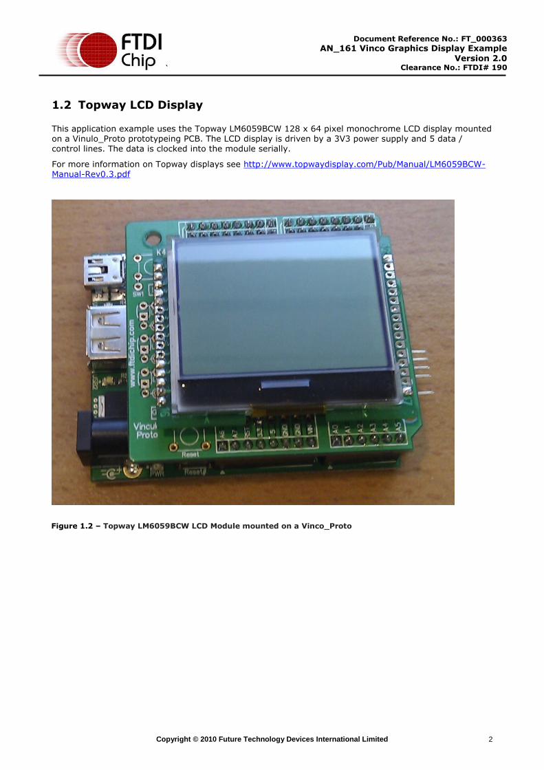
1.2 Topway LCD Display
This application example uses the Topway LM6059BCW 128 x 64 pixel monochrome LCD display mounted on a Vinulo_Proto prototypeing PCB. The LCD display is driven by a 3V3 power supply and 5 data / control lines. The data is clocked into the module serially.
For more information on Topway displays see http://www.topwaydisplay.com/Pub/Manual/LM6059BCW-Manual-Rev0.3.pdf
Figure 1.2 – Topway LM6059BCW LCD Module mounted on a Vinco_Proto
`
Copyright © 2010 Future Technology Devices International Limited 3
Document Reference No.: FT_000363
AN_161 Vinco Graphics Display Example
Version 2.0 Clearance No.: FTDI# 190
Table of Contents
1 Introduction .................................................................... 1
1.1 VNC2 Devices ............................................................................ 1
1.2 Topway LCD Display .................................................................. 2
2 Block Diagram ................................................................. 4
3 Interconnect ................................................................... 5
3.1 Power ....................................................................................... 5
3.2 LCD Control ............................................................................... 5
3.3 Debugger Interface ................................................................... 6
3.3.1 Signal Description - Debugger Interface ....................................................... 6
4 Source code for the VNC2 writing to LCD Display ............ 7
4.1 VNC2 Initialisation .................................................................... 7
4.2 LCD Initialisation ...................................................................... 8
4.3 Writing Command Instructions to the LCD ................................ 9
4.4 Writing Data Bytes to the LCD Display ...................................... 9
4.5 Switching on the LCD Display .................................................. 10
4.6 Switching off the LCD Display ................................................. 10
4.7 Setting the LCD Contrast ......................................................... 10
4.8 Addressing the LCD ................................................................. 11
4.9 Clearing the Display ................................................................ 11
4.10 Displaying a graphical Logo .................................................... 12
4.11 Displaying a line of text .......................................................... 13
4.12 Displaying another line of text ................................................ 14
4.13 The Firmware function ............................................................ 15
5 Programming Vinco ....................................................... 18
6 Running the firmware ................................................... 19
7 Contact Information ...................................................... 20
Appendix A – References ................................................................. 21
http://www.avrportal.com/?page=image2glcd .............................. 21
Appendix B – List of Figures and Tables .......................................... 22
List of Figures ................................................................................. 22
List of Tables ................................................................................... 22
Appendix C – Revision History ......................................................... 23
Appendix D Legal Disclaimer: ............................................. 24
`
Copyright © 2010 Future Technology Devices International Limited 4
Document Reference No.: FT_000363
AN_161 Vinco Graphics Display Example
Version 2.0 Clearance No.: FTDI# 190
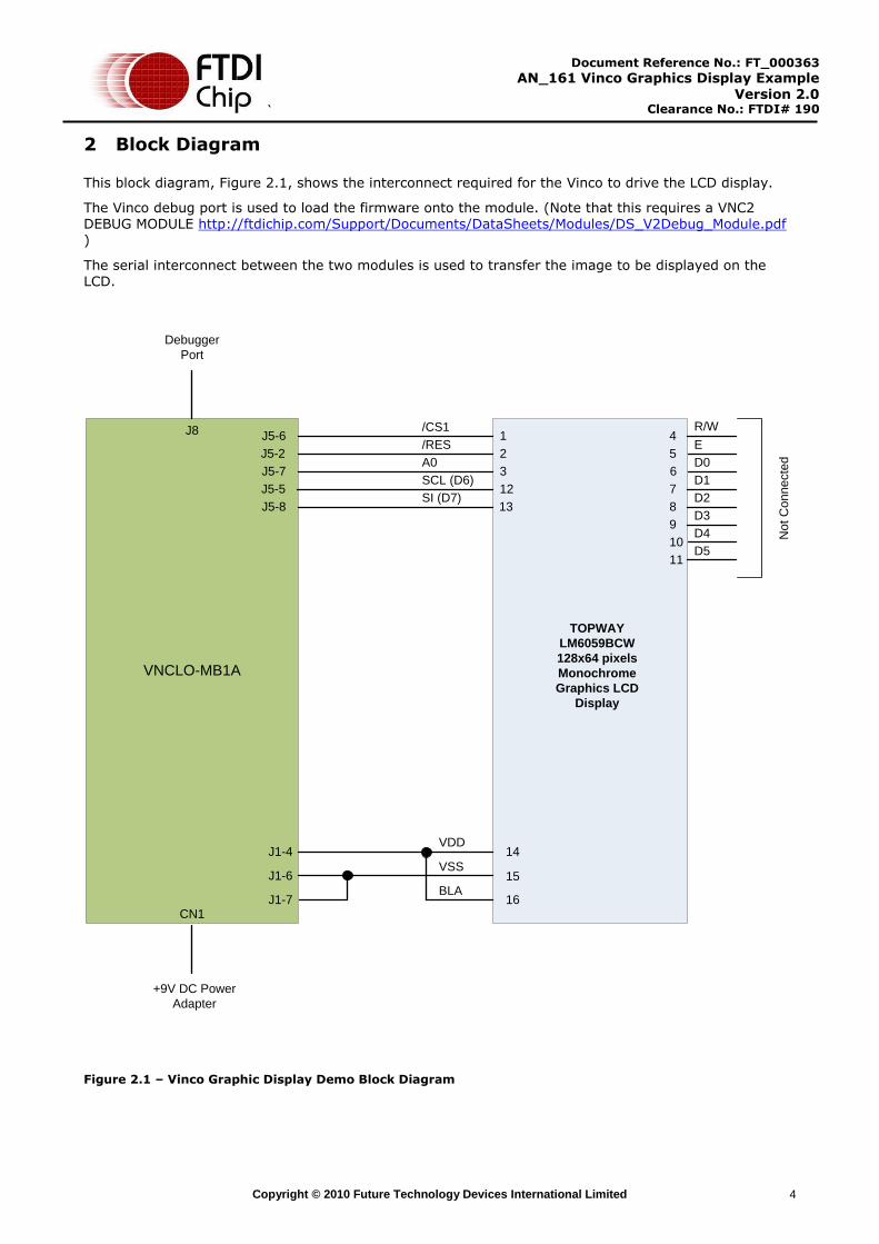
2 Block Diagram
This block diagram, Figure 2.1, shows the interconnect required for the Vinco to drive the LCD display.
The Vinco debug port is used to load the firmware onto the module. (Note that this requires a VNC2 DEBUG MODULE http://ftdichip.com/Support/Documents/DataSheets/Modules/DS_V2Debug_Module.pdf )
The serial interconnect between the two modules is used to transfer the image to be displayed on the LCD.
VNCLO-MB1A
J8
TOPWAY
LM6059BCW
128x64 pixels
Monochrome
Graphics LCD
Display
Debugger
Port
CN1
+9V DC Power
Adapter
J1-4
J1-6
1
2
12
13
/CS1
/RES
SCL (D6)
SI (D7)
14VDD
15VSS
16BLA
J1-7
J5-6
J5-2
J5-7
J5-8
4
5
6
7
8
9
10
11
A0
R/W
E
D0
D1
D2
D3
D4
D5
No
t C
on
ne
cte
d
J5-5
3
Figure 2.1 – Vinco Graphic Display Demo Block Diagram
`
Copyright © 2010 Future Technology Devices International Limited 5
Document Reference No.: FT_000363
AN_161 Vinco Graphics Display Example
Version 2.0 Clearance No.: FTDI# 190
3 Interconnect
3.1 Power
The Vinco module may be powered from the USB port on CN3 (5V) or via an external power converter (9V/1A DC) to CN1 (for example the FTDI VNCLO-PSU-UK)
As this application provides power to external circuitry (the LCD display), the Vinco is powered from an external 9V supply.
To ensure this power source is routed to the PCB, JP1 on the Vinco module must be set to the 2-3 position.
Power from the Vinco module is taken from J1 pin 4 to give a +3V3 supply for the Topway LCD display.
3.2 LCD Control
The Topway LCD display may be controlled in either a synchronous serial data mode or an 8-bit data mode. This application uses the serial mode. The signals defined in the block diagram in section 2 are described in Table 3.1.
Signal Function
/CS1 Active low chip select for the LCD module
/RES Active low reset for the LCD module
A0
Register select for the LCD module.
0 = Display data
1 = Control data
SCL Serial clock input to LCD module.
SI Serial data input to LCD module.
BLA Positive supply for LCD Backlight.
Table 3.1 - Signal Name and Description – LCD Interface
`
Copyright © 2010 Future Technology Devices International Limited 6
Document Reference No.: FT_000363
AN_161 Vinco Graphics Display Example
Version 2.0 Clearance No.: FTDI# 190
3.3 Debugger Interface
The purpose of the debugger interface is to provide access to the VNC2 silicon/firmware debugger. The debug interface can be accessed by connecting a VNC2_Debug_Module (http://www.ftdichip.com/Support/Documents/DataSheets/ICs/DS_Vinculum-II.pdf ) to the J8 connector. This debug module gives access to the debugger through a USB connection to a PC via the Integrated
Development Environment (IDE). The IDE is a graphical interface to the VNC2 software development tool-chain and gives the following debug capabilities through the debugger interface:
Flash Erase, Write and Program. Application debug - application code can have breakpoints, be single stepped and can be halted. Detailed internal debug - memory and register read/write access.
The IDE may be downloaded, free of charge, from http://www.ftdichip.com/Firmware/V2TC/VNC2toolchain.htm
The Debugger Interface, and how to use it, is further described in the following applications Note
Vinculum-II Debug Interface Description
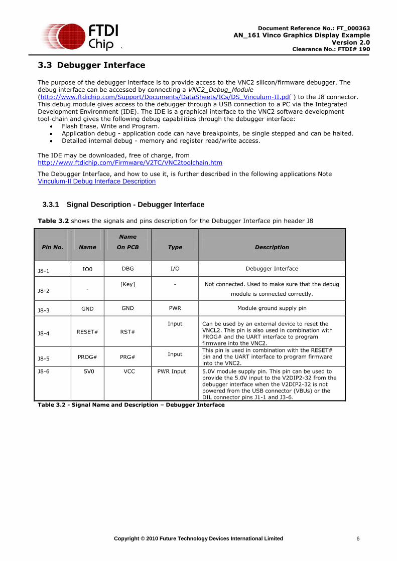
3.3.1 Signal Description - Debugger Interface
Table 3.2 shows the signals and pins description for the Debugger Interface pin header J8
Pin No.
Name
Name
On PCB
Type
Description
J8-1 IO0 DBG I/O Debugger Interface
J8-2 - [Key] - Not connected. Used to make sure that the debug
module is connected correctly.
J8-3 GND GND PWR Module ground supply pin
J8-4 RESET# RST#
Input Can be used by an external device to reset the VNCL2. This pin is also used in combination with PROG# and the UART interface to program firmware into the VNC2.
J8-5 PROG# PRG# Input
This pin is used in combination with the RESET# pin and the UART interface to program firmware into the VNC2.
J8-6 5V0 VCC
PWR Input 5.0V module supply pin. This pin can be used to provide the 5.0V input to the V2DIP2-32 from the debugger interface when the V2DIP2-32 is not powered from the USB connector (VBUs) or the DIL connector pins J1-1 and J3-6.
Table 3.2 - Signal Name and Description – Debugger Interface
`
Copyright © 2010 Future Technology Devices International Limited 7
Document Reference No.: FT_000363
AN_161 Vinco Graphics Display Example
Version 2.0 Clearance No.: FTDI# 190
4 Source code for the VNC2 writing to LCD Display
The Vinculum II IDE is used to create application code to run on VNC2. This section gives some example source code, and explains its operation, used to drive the LCD display via the Vinco module.
Note the full project can be downloaded from: http://ftdichip.com/Support/SoftwareExamples/VinculumIIProjects.htm
4.1 VNC2 Initialisation
When generating firmware for VNC2, the first steps are to enable the Vinculum Operating System (VOS), which controls the VNC2 services and device manager, defines the clock speed the core will use, and defines the VNC2 pins that will be used. This is done in the function labelled main. The “main” function
for this application is shown as follows
void main(void)
{
// GPIO context structure
gpio_context_t gpioCtx;
// SPI Master context structure
spimaster_context_t spimCtx;
// call VOS initialisation routines
vos_init(10, VOS_TICK_INTERVAL, NUMBER_OF_DEVICES);
vos_set_clock_frequency(VOS_48MHZ_CLOCK_FREQUENCY);
// Setup IOMUX
// Control port = GPIO PORT_B
vos_iomux_define_output(63,IOMUX_OUT_GPIO_PORT_B_2); // PortB_2->LCD_RST#
vos_iomux_define_output(13,IOMUX_OUT_GPIO_PORT_B_6); // PortB_6->LCD_A0
// SPI pins
vos_iomux_define_output(14,IOMUX_OUT_SPI_MASTER_CS_0); // LCD_CS#
vos_iomux_define_output(15,IOMUX_OUT_SPI_MASTER_CLK); // LCD_CLK
vos_iomux_define_output(16,IOMUX_OUT_SPI_MASTER_MOSI); // LCD_SDI
// initialise device drivers
spimCtx.buffer_size = VOS_BUFFER_SIZE_128_BYTES;
spimaster_init(VOS_DEV_SPIM,&spimCtx);
gpioCtx.port_identifier = GPIO_PORT_B;
gpio_init(VOS_DEV_GPIOB,&gpioCtx);
// create threads for firmware application (no parameters)
tcbFirmware = vos_create_thread(29, SIZEOF_THREAD_MEMORY, firmware, 0);
// start VOS scheduler
vos_start_scheduler();
`
Copyright © 2010 Future Technology Devices International Limited 8
Document Reference No.: FT_000363
AN_161 Vinco Graphics Display Example
Version 2.0 Clearance No.: FTDI# 190
main_loop:
goto main_loop;
}
Note: Starting the VOS scheduler is always the last thing to be done as all configuration must be complete before this starts.
4.2 LCD Initialisation
The LCD must be put into an initial known state to be able to accept new data and this initialisation is done in the lcd_ini function.
void lcd_ini(void)
{
unsigned char data_byte;
// Hardware reset
data_byte = (0xFF&(~LCD_RST));
vos_dev_write(hGpioB,&data_byte,1,NULL); // LCD Reset line - low
vos_delay_msecs(5);
data_byte = (data_byte|LCD_RST);
vos_dev_write(hGpioB,&data_byte,1,NULL); // LCD Reset line - high
vos_delay_msecs(5);
cmd_buffer[0] = CMD_DISP_SET_BIAS; // Send 'Set Bias' command
cmd_buffer[1] = CMD_DISP_SCANDIR; // Send 'ADC Normal' command
cmd_buffer[2] = CMD_DISP_REV|0x08; // Send 'Flip on Y' command
cmd_buffer[3] = CMD_DISP_LINE_ADDR; // Send 'Line addr = 0' command
write_lcd_cmd(cmd_buffer, 4);
cmd_buffer[0] = CMD_DISP_PWRCTRL|LCD_VCNV; // Send 'Power Ctrl' command
write_lcd_cmd(cmd_buffer, 1);
vos_delay_msecs(50);
cmd_buffer[0] = cmd_buffer[0]|LCD_VREG;
write_lcd_cmd(cmd_buffer, 1);
vos_delay_msecs(50);
cmd_buffer[0] = cmd_buffer[0]|LCD_VFOL;
write_lcd_cmd(cmd_buffer, 1);
vos_delay_msecs(50);
cmd_buffer[0] = CMD_DISP_VREG_RES_RATIO|0x06; // Send 'Regulator Resistor Select' command
cmd_buffer[1] = CMD_DISP_EVOLUME_MODE; // Send 'Set Reference Voltage' command
cmd_buffer[2] = LCD_EVOLUME_VALUE;
cmd_buffer[3] = CMD_DISP_ON; // Send 'Display On' command
`
Copyright © 2010 Future Technology Devices International Limited 9
Document Reference No.: FT_000363
AN_161 Vinco Graphics Display Example
Version 2.0 Clearance No.: FTDI# 190
write_lcd_cmd(cmd_buffer, 4);
vos_delay_msecs(50);
lcd_clear();
SetPageAddress(0);
SetColumnAddress(0);
SetLineAddress(0);
}
The data values which can be sent to the LCD are defined in the LCD user manual. The
write_lcd_cmd(cmd_buffer, 1);) is an instruction to call the write_LCD_cmd function so that data may be is moved from the VNC2 to the LCD over the VNC2 SPI interface.
4.3 Writing Command Instructions to the LCD
void write_lcd_cmd(unsigned char *cmd, unsigned char len)
{
unsigned char ctrl_byte;
ctrl_byte = (~LCD_A0)|LCD_RST;
vos_dev_write(hGpioB,&ctrl_byte,1,NULL); // Set A0 and RESET line high
spim_iocb.ioctl_code = VOS_IOCTL_SPI_MASTER_SS_0;
spim_iocb.set.param = SPI_MASTER_SS_ENABLE;
vos_dev_ioctl(hSPIm,&spim_iocb);
vos_dev_write(hSPIm, cmd, (len&0x00FF), NULL);
spim_iocb.ioctl_code = VOS_IOCTL_SPI_MASTER_SS_0;
spim_iocb.set.param = SPI_MASTER_SS_DISABLE;
vos_dev_ioctl(hSPIm,&spim_iocb);
}
vos_dev_write is a VOS defined command for writing out data. The hGPIO is the handle for the GPIO driver that is used to control the A0 and RESET pins of the LCD. The hSPIm is the handle for the SPI
master driver that is used to send the clocked serial data to the LCD display .
4.4 Writing Data Bytes to the LCD Display
The main difference with writing data to the LCD as opposed to commands is the state of the A0 pin controlled by the VNC2 GPIO.
void write_lcd_data(unsigned char *data, unsigned char len)
{
unsigned char ctrl_byte;
ctrl_byte = LCD_A0|LCD_RST;
`
Copyright © 2010 Future Technology Devices International Limited 10
Document Reference No.: FT_000363
AN_161 Vinco Graphics Display Example
Version 2.0 Clearance No.: FTDI# 190
vos_dev_write(hGpioB,&ctrl_byte,1,NULL); // Set A0 low and RESET line high
spim_iocb.ioctl_code = VOS_IOCTL_SPI_MASTER_SS_0;
spim_iocb.set.param = SPI_MASTER_SS_ENABLE;
vos_dev_ioctl(hSPIm,&spim_iocb);
vos_dev_write(hSPIm, data, (len&0x00FF), NULL);
spim_iocb.ioctl_code = VOS_IOCTL_SPI_MASTER_SS_0;
spim_iocb.set.param = SPI_MASTER_SS_DISABLE;
vos_dev_ioctl(hSPIm,&spim_iocb);
}
4.5 Switching on the LCD Display
This is switching on the LCD backlight.
void lcd_on(void)
{
cmd_buffer[0] = CMD_DISP_ON; // Send 'Display On' command
write_lcd_cmd(cmd_buffer, 1);
}
4.6 Switching off the LCD Display
This is switching off the LCD backlight.
void lcd_off(void)
{
cmd_buffer[0] = CMD_DISP_OFF; // Send 'Display Off' command
write_lcd_cmd(cmd_buffer, 1);
}
4.7 Setting the LCD Contrast
This is sending a command to the LCD display to define how bright the image appears.
void lcd_set_contrast(unsigned char contrast_value)
{
cmd_buffer[0] = CMD_DISP_EVOLUME_MODE; // Send 'Set Reference Voltage' command
cmd_buffer[1] = contrast_value;
write_lcd_cmd(cmd_buffer, 2);
}
`
Copyright © 2010 Future Technology Devices International Limited 11
Document Reference No.: FT_000363
AN_161 Vinco Graphics Display Example
Version 2.0 Clearance No.: FTDI# 190
4.8 Addressing the LCD
The LCD is notionally like a large memory where each memory location equals a pixel. You can address this memory (pixel) by pages or by lines and columns. The following functions provide the addressing information.
void SetPageAddress(unsigned char page)
{
cmd_buffer[0] = CMD_DISP_PAGE_ADDR | (page &0x0F);
write_lcd_cmd(cmd_buffer, 1);
}
//---------------------------------------------------------
void SetColumnAddress(unsigned char column)
{
cmd_buffer[0] = CMD_DISP_COLADDR_H | (column>>4);
cmd_buffer[1] = CMD_DISP_COLADDR_L | (column&0x0F);
write_lcd_cmd(cmd_buffer, 2);
}
//---------------------------------------------------------
void SetLineAddress(unsigned char line)
{
cmd_buffer[0] = CMD_DISP_LINE_ADDR | line;
write_lcd_cmd(cmd_buffer, 1);
}
4.9 Clearing the Display
Using the following functions the LCD display can be cleared or have individual lines cleared.
void lcd_clear(void)
{
unsigned char i;
for(i=0;i<128;i++)
{
lcd_buffer[i]=0;
}
for(i=0;i<8;i++)
{
SetPageAddress(i);
SetColumnAddress(0);
SetLineAddress(0);
write_lcd_data(lcd_buffer, 128);
}
`
Copyright © 2010 Future Technology Devices International Limited 12
Document Reference No.: FT_000363
AN_161 Vinco Graphics Display Example
Version 2.0 Clearance No.: FTDI# 190
}
//---------------------------------------------------------
void lcd_clear_line(unsigned char y)
{
unsigned char i;
for(i=0;i<128;i++)
{
lcd_buffer[i]=0;
}
SetPageAddress(y);
SetColumnAddress(0);
write_lcd_data(lcd_buffer, 128);
}
4.10 Displaying a graphical Logo
IMAGE2GLCD is a free tool from the internet used to create a graphical bitmap. The bitmap generated in this project was the Vinculum logo which was stored in V2Logo.h for printing out to the LCD screen with this function.
void show_logo(unsigned short delay1)
{
unsigned char i,j;
unsigned short temp;
SetPageAddress(0);
SetColumnAddress(0);
for (j=0;j<8;j++)
{
SetPageAddress(j);
SetColumnAddress(0);
for (i=0;i<128;i++)
{
temp=128*j;
temp+=i;
lcd_buffer[i]= img[temp];
}
write_lcd_data(lcd_buffer,128);
vos_delay_msecs(delay1);
}
}
`
Copyright © 2010 Future Technology Devices International Limited 13
Document Reference No.: FT_000363
AN_161 Vinco Graphics Display Example
Version 2.0 Clearance No.: FTDI# 190
4.11 Displaying a line of text
As well as graphics this example shows how to display text with different font sizes.
This function uses a character bit map 8x8 pixels in size.
void LCDprintf8x8(unsigned char x,unsigned char y,unsigned char inv,unsigned char *Str)
{
unsigned char m,n;
unsigned short yy;
SetPageAddress(y); // Line where to display the string (0..7)
SetColumnAddress(x); // Horizontal offset (0..127)
n=x;
while(*Str != '\0') // While not the end of the string
{
if((n+8)>127) // Check if one more character can be displayed
{
break;
}
else
{
yy = *Str; // Get ASCII value
yy = (yy*8); // Calculate the position of charecter bitmap
for(m=0; m<8; m++)
{
lcd_buffer[n]= font8x8[yy+m]; // Copy character bitmap to display buffer
if(inv)
{
lcd_buffer[n]= (~lcd_buffer[n]); // Copy character bitmap to display buffer
}
n++;
}
++Str; // Increment the pointer
}
}
write_lcd_data(lcd_buffer, (n+1)); // Send buffer to the display.
}
`
Copyright © 2010 Future Technology Devices International Limited 14
Document Reference No.: FT_000363
AN_161 Vinco Graphics Display Example
Version 2.0 Clearance No.: FTDI# 190
4.12 Displaying another line of text
This function uses a character bit map 5x7 pixels in size. This is equivalent to creating a different font.
void LCDprintf5x7(unsigned char x,unsigned char y,unsigned char inv,unsigned char *Str)
{
unsigned char m,n;
unsigned short yy;
SetPageAddress(y); // Line where to display the string (0..7)
SetColumnAddress(x); // Horizontal offset (0..127)
n=x;
while(*Str != '\0') // While not the end of the string
{
if((n+5)>127) // Check if one more character can be displayed
{
break;
}
else
{
yy = *Str; // Get ASCII value
yy = (yy-32)*5; // Calculate the position of charecter bitmap
for(m=0; m<5; m++)
{
lcd_buffer[n]= font5x7[yy+m]; // Copy character bitmap to display buffer
if(inv)
{
lcd_buffer[n]= (~lcd_buffer[n]); // Copy character bitmap to display buffer
}
n++;
}
++Str; // Increment the pointer
}
}
write_lcd_data(lcd_buffer, (n+1)); // Send buffer to the display.
}
`
Copyright © 2010 Future Technology Devices International Limited 15
Document Reference No.: FT_000363
AN_161 Vinco Graphics Display Example
Version 2.0 Clearance No.: FTDI# 190
4.13 The Firmware function
This function is the main thread calling all the other functions to create a scrolling display.
void firmware(void)
{
// GPIO IOCTL request block
gpio_ioctl_cb_t gpio_iocb;
// general purpose variables
unsigned char i;
// find and open GPIO device port B
hGpioB = vos_dev_open(VOS_DEV_GPIOB);
gpio_iocb.ioctl_code = VOS_IOCTL_GPIO_SET_MASK;
gpio_iocb.value = 0x44; // set bit 2 and 6 as outputs, all other as
inputs
vos_dev_ioctl(hGpioB, &gpio_iocb);
//*********************************************************
// INITIALISE SPI MASTER PARAMETERS
//*********************************************************
// open SPI Master and get a handle
hSPIm = vos_dev_open(VOS_DEV_SPIM);
// enable DMA
spim_iocb.ioctl_code = VOS_IOCTL_COMMON_ENABLE_DMA;
vos_dev_ioctl(hSPIm,&spim_iocb);
// set clock phase
spim_iocb.ioctl_code = VOS_IOCTL_SPI_MASTER_SCK_CPHA;
spim_iocb.set.param = SPI_MASTER_SCK_CPHA_1;
vos_dev_ioctl(hSPIm,&spim_iocb);
// set clock polarity
spim_iocb.ioctl_code = VOS_IOCTL_SPI_MASTER_SCK_CPOL;
spim_iocb.set.param = SPI_MASTER_SCK_CPOL_1;
vos_dev_ioctl(hSPIm,&spim_iocb);
// set data order
spim_iocb.ioctl_code = VOS_IOCTL_SPI_MASTER_DATA_ORDER;
spim_iocb.set.param = SPI_MASTER_DATA_ORDER_MSB;
vos_dev_ioctl(hSPIm,&spim_iocb);
// set clock rate
spim_iocb.ioctl_code = VOS_IOCTL_SPI_MASTER_SET_SCK_FREQUENCY;
spim_iocb.set.spi_master_sck_freq = 1000000;
vos_dev_ioctl(hSPIm,&spim_iocb);
spim_iocb.ioctl_code = VOS_IOCTL_SPI_MASTER_SET_DATA_DELAY;
spim_iocb.set.param = 0;
vos_dev_ioctl(hSPIm,&spim_iocb);
// set chip select
spim_iocb.ioctl_code = VOS_IOCTL_SPI_MASTER_SS_0;
spim_iocb.set.param = SPI_MASTER_SS_DISABLE;
vos_dev_ioctl(hSPIm,&spim_iocb);
spim_iocb.ioctl_code = VOS_IOCTL_SPI_MASTER_SS_1;
`
Copyright © 2010 Future Technology Devices International Limited 16
Document Reference No.: FT_000363
AN_161 Vinco Graphics Display Example
Version 2.0 Clearance No.: FTDI# 190
spim_iocb.set.param = SPI_MASTER_SS_DISABLE;
vos_dev_ioctl(hSPIm,&spim_iocb);
lcd_ini();
while(1)
{
lcd_clear();
show_logo(200);
vos_delay_msecs(2000);
i = LCD_EVOLUME_VALUE;
while(i>0)
{
lcd_set_contrast(i);
i--;
vos_delay_msecs(100);
}
lcd_off();
lcd_clear();
LCDprintf8x8(0,1,0,LINE1);
LCDprintf8x8(0,2,0,LINE2);
LCDprintf5x7(0,3,0,LINE3);
LCDprintf5x7(0,4,0,LINE4);
lcd_on();
i=0;
while(i<(LCD_EVOLUME_VALUE+1))
{
lcd_set_contrast(i);
i++;
vos_delay_msecs(100);
}
vos_delay_msecs(1000);
for(i=0;i<3;i++)
{
lcd_off();
vos_delay_msecs(330);
lcd_on();
vos_delay_msecs(660);
}
// Shift display 8 lines up
for(i=0;i<8;i++)
{
SetLineAddress(i);
vos_delay_msecs(200);
}
lcd_clear_line(1);
LCDprintf5x7(0,0,0,LINE5);
// Shift display 8 lines up
for(i=0;i<8;i++)
{
SetLineAddress(i+8);
vos_delay_msecs(200);
}
lcd_clear_line(2);
LCDprintf5x7(0,1,0,LINE6);
for(i=0;i<8;i++)
{
SetLineAddress(i+16);
vos_delay_msecs(200);
}
lcd_clear_line(3);
`
Copyright © 2010 Future Technology Devices International Limited 17
Document Reference No.: FT_000363
AN_161 Vinco Graphics Display Example
Version 2.0 Clearance No.: FTDI# 190
LCDprintf5x7(0,2,0,LINE7);
for(i=0;i<8;i++)
{
SetLineAddress(i+24);
vos_delay_msecs(200);
}
lcd_clear_line(4);
LCDprintf5x7(0,3,0,LINE8);
for(i=0;i<8;i++)
{
SetLineAddress(i+32);
vos_delay_msecs(200);
}
lcd_clear_line(5);
LCDprintf5x7(0,4,0,LINE9);
for(i=0;i<8;i++)
{
SetLineAddress(i+40);
vos_delay_msecs(200);
}
lcd_clear_line(6);
LCDprintf5x7(0,5,0,LINE10);
for(i=0;i<8;i++)
{
SetLineAddress(i+48);
vos_delay_msecs(200);
}
lcd_clear_line(7);
LCDprintf5x7(0,6,0,LINE11);
for(i=0;i<8;i++)
{
SetLineAddress(i+56);
vos_delay_msecs(200);
}
lcd_clear_line(0);
LCDprintf5x7(0,7,0,LINE12);
vos_delay_msecs(2000);
}
}
`
Copyright © 2010 Future Technology Devices International Limited 18
Document Reference No.: FT_000363
AN_161 Vinco Graphics Display Example
Version 2.0 Clearance No.: FTDI# 190
5 Programming Vinco
When Vinco has been connected to the LCD panel and the firmware has been built in the IDE, the next step is to transfer the .ROM file generated by the IDE to the Vinco module. The IDE generates the .ROM file with a single button click of the “Build” button.
Connect the USB port of the VNC2 Debug Module to a PC and load the free FTDI drivers for the FT232R device on the debug module. This will happen automatically via Windows Update if you are connected to their internet. Otherwise refer to the installation guide for your OS:
http://www.ftdichip.com/Support/Documents/InstallGuides.htm
The IDE should now automatically detect the VNC2 debug module.
Connect the other end of the VNC2 Debug Module to the J8 connector of the Vinco.
Use the IDE FLASH button to load the .ROM file into the Vinco. A getting started guide for using the Vinculum IDE may be downloaded from:
http://www.ftdichip.com/Support/Documents/AppNotes/AN_142_Vinculum-II_Tool_Chain_Getting_Started_Guide.pdf
The IDE will report back a successful programming. At this point the VNC2 Debug module may be removed from the Vinco J8 connector.
The .rom file can also be downloaded from the following location:
http://ftdichip.com/Support/SoftwareExamples/VinculumIIProjects.htm
`
Copyright © 2010 Future Technology Devices International Limited 19
Document Reference No.: FT_000363
AN_161 Vinco Graphics Display Example
Version 2.0 Clearance No.: FTDI# 190
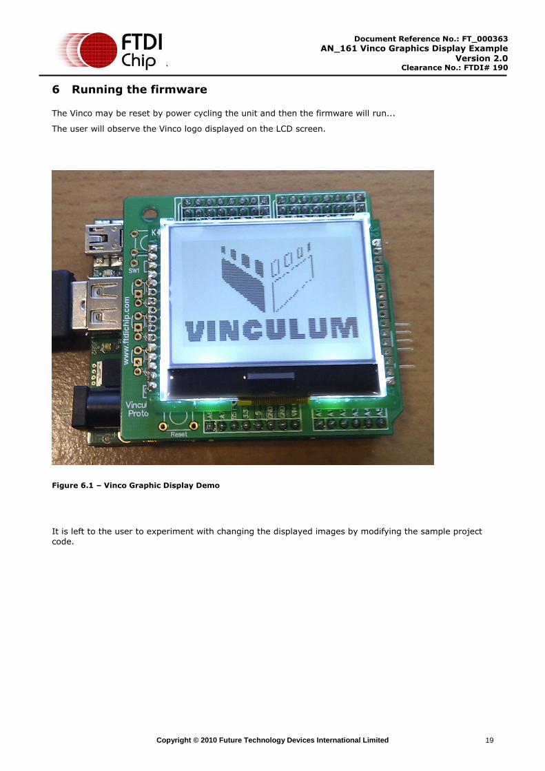
6 Running the firmware
The Vinco may be reset by power cycling the unit and then the firmware will run...
The user will observe the Vinco logo displayed on the LCD screen.
Figure 6.1 – Vinco Graphic Display Demo
It is left to the user to experiment with changing the displayed images by modifying the sample project
code.
`
Copyright © 2010 Future Technology Devices International Limited 20
Document Reference No.: FT_000363
AN_161 Vinco Graphics Display Example
Version 2.0 Clearance No.: FTDI# 190
7 Contact Information Head Office – Glasgow, UK Future Technology Devices International Limited Unit 1, 2 Seaward Place, Centurion Business Park Glasgow, G41 1HH United Kingdom Tel: +44 (0) 141 429 2777 Fax: +44 (0) 141 429 2758
E-mail (Sales) [email protected] E-mail (Support) [email protected] E-mail (General Enquiries) [email protected] Web Site URL http://www.ftdichip.com Web Shop URL http://www.ftdichip.com
Branch Office – Taipei, Taiwan Future Technology Devices International Limited (Taiwan) 2F, No 516, Sec. 1 NeiHu Road Taipei 114 Taiwan, R.O.C. Tel: +886 (0) 2 8791 3570 Fax: +886 (0) 2 8791 3576 E-mail (Sales) [email protected] E-mail (Support) [email protected] E-mail (General Enquiries) [email protected] Web Site URL http://www.ftdichip.com
Branch Office – Hillsboro, Oregon, USA Future Technology Devices International Limited (USA) 7235 NW Evergreen Parkway, Suite 600 Hillsboro, OR 97123-5803 USA Tel: +1 (503) 547 0988 Fax: +1 (503) 547 0987 E-Mail (Sales) [email protected] E-Mail (Support) [email protected] E-Mail (General Enquiries) [email protected] Web Site URL http://www.ftdichip.com Branch Office – Shanghai, China
Future Technology Devices International Limited (China) Room 408, 317 Xianxia Road, ChangNing District, ShangHai, China
Tel: +86 (21) 62351596 Fax: +86(21) 62351595 E-Mail (Sales): [email protected] E-Mail (Support): [email protected] E-Mail (General Enquiries): [email protected] Web Site URL http://www.ftdichip.com
Distributor and Sales Representatives
Please visit the Sales Network page of the FTDI Web site for the contact details of our distributor(s) and sales representative(s) in your country.
`
Copyright © 2010 Future Technology Devices International Limited 21
Document Reference No.: FT_000363
AN_161 Vinco Graphics Display Example
Version 2.0 Clearance No.: FTDI# 190
Appendix A – References
Application and Technical Notes available at http://www.ftdichip.com/Support/Documents/AppNotes.htm
Vinco datasheet
http://www.ftdichip.com/Support/Documents/DataSheets/ICs/DS_Vinculum-II.pdf
VNC2 Debug Module
http://www.ftdichip.com/Support/Documents/DataSheets/ICs/DS_Vinculum-II.pdf
Vinculum-II IO Cell Description
http://www.ftdichip.com/Support/Documents/AppNotes/AN_137_Vinculum-II%20IO_Cell_Description.pdf
Vinculum-II Debug Interface Description
http://www.ftdichip.com/Support/Documents/AppNotes/AN_138_Vinculum-II_Debug_Interface_Description.pdf
Vinculum-II IO Mux Explained
http://www.ftdichip.com/Support/Documents/AppNotes/AN_139_Vinculum-II%20IO_Mux%20Explained.pdf
Vinculum-II Errata Technical Note
http://www.ftdichip.com/Support/Documents/TechnicalNotes/TN_118_VNC2%20Errata%20Technical%20Note.pdf
Topway LMBABC Display
http://www.topwaydisplay.com/Pub/Manual/LM6059BCW-Manual-Rev0.3.pdf
IMAGE2GLCD utility for creating bit map
http://www.avrportal.com/?page=image2glcd
`
Copyright © 2010 Future Technology Devices International Limited 22
Document Reference No.: FT_000363
AN_161 Vinco Graphics Display Example
Version 2.0 Clearance No.: FTDI# 190
Appendix B – List of Figures and Tables
List of Figures
Figure 1.1 - VINCO ....................................................................................................................... 1
Figure 1.2 – Topway LM6059BCW LCD Module mounted on a Vinco_Proto ........................................... 2
Figure 2.1 – Vinco Graphic Display Demo Block Diagram ................................................................... 4
Figure 6.1 – Vinco Graphic Display Demo ....................................................................................... 19
List of Tables
Table 3.1 - Signal Name and Description – LCD Interface .................................................................. 5
Table 3.2 - Signal Name and Description – Debugger Interface .......................................................... 6
`
Copyright © 2010 Future Technology Devices International Limited 23
Document Reference No.: FT_000363
AN_161 Vinco Graphics Display Example
Version 2.0 Clearance No.: FTDI# 190
Appendix C – Revision History
Version 1.0 First Release 26th November 2010
Version 2.0 Changed Vinculo brand name to Vinco 14th April 2011
`
Copyright © 2010 Future Technology Devices International Limited 24
Document Reference No.: FT_000363
AN_161 Vinco Graphics Display Example
Version 2.0 Clearance No.: FTDI# 190
Appendix D Legal Disclaimer:
System and equipment manufacturers and designers are responsible to ensure that their systems, and any Future Technology Devices International Ltd (FTDI) devices incorporated in their systems, meet all applicable safety, regulatory and system-level performance requirements. All application-related information in this document (including application descriptions, suggested FTDI devices and other
materials) is provided for reference only. While FTDI has taken care to assure it is accurate, this information is subject to customer confirmation, and FTDI disclaims all liability for system designs and for any applications assistance provided by FTDI. Use of FTDI devices in life support and/or safety applications is entirely at the user’s risk, and the user agrees to defend, indemnify and hold harmless FTDI from any and all damages, claims, suits or expense resulting from such use. This document is subject to change without notice. No freedom to use patents or other intellectual property rights is
implied by the publication of this document. Neither the whole nor any part of the information contained in, or the product described in this document, may be adapted or reproduced in any material or electronic form without the prior written consent of the copyright holder. Future Technology Devices International Ltd, Unit 1, 2 Seaward Place, Centurion Business Park, Glasgow G41 1HH, United Kingdom. Scotland
Registered Company Number: SC136640


![AN 161 Vinco Graphics Display Example · 2016. 7. 26. · J8-2 - [Key] - Not connected. Used to make sure that the debug module is connected correctly. J8-3 GND PWR Module ground](https://img.dokumen.tips/doc/110x75/60b3c1541956224a9a0aaff0/an-161-vinco-graphics-display-example-2016-7-26-j8-2-key-not-connected.jpg)